US9035439B2 - Apparatus, system and method for use in mounting electronic elements - Google Patents
Apparatus, system and method for use in mounting electronic elementsDownload PDFInfo
- Publication number
- US9035439B2 US9035439B2US12/695,978US69597810AUS9035439B2US 9035439 B2US9035439 B2US 9035439B2US 69597810 AUS69597810 AUS 69597810AUS 9035439 B2US9035439 B2US 9035439B2
- Authority
- US
- United States
- Prior art keywords
- casing
- lead
- indentation
- chipset
- recess
- Prior art date
- Legal status (The legal status is an assumption and is not a legal conclusion. Google has not performed a legal analysis and makes no representation as to the accuracy of the status listed.)
- Active
Links
Images


Classifications
- H—ELECTRICITY
- H05—ELECTRIC TECHNIQUES NOT OTHERWISE PROVIDED FOR
- H05K—PRINTED CIRCUITS; CASINGS OR CONSTRUCTIONAL DETAILS OF ELECTRIC APPARATUS; MANUFACTURE OF ASSEMBLAGES OF ELECTRICAL COMPONENTS
- H05K5/00—Casings, cabinets or drawers for electric apparatus
- H05K5/0091—Housing specially adapted for small components
- H01L33/486—
- H01L33/62—
- H—ELECTRICITY
- H10—SEMICONDUCTOR DEVICES; ELECTRIC SOLID-STATE DEVICES NOT OTHERWISE PROVIDED FOR
- H10H—INORGANIC LIGHT-EMITTING SEMICONDUCTOR DEVICES HAVING POTENTIAL BARRIERS
- H10H20/00—Individual inorganic light-emitting semiconductor devices having potential barriers, e.g. light-emitting diodes [LED]
- H10H20/80—Constructional details
- H10H20/85—Packages
- H10H20/8506—Containers
- H—ELECTRICITY
- H10—SEMICONDUCTOR DEVICES; ELECTRIC SOLID-STATE DEVICES NOT OTHERWISE PROVIDED FOR
- H10H—INORGANIC LIGHT-EMITTING SEMICONDUCTOR DEVICES HAVING POTENTIAL BARRIERS
- H10H20/00—Individual inorganic light-emitting semiconductor devices having potential barriers, e.g. light-emitting diodes [LED]
- H10H20/80—Constructional details
- H10H20/85—Packages
- H10H20/857—Interconnections, e.g. lead-frames, bond wires or solder balls
- H—ELECTRICITY
- H01—ELECTRIC ELEMENTS
- H01L—SEMICONDUCTOR DEVICES NOT COVERED BY CLASS H10
- H01L2224/00—Indexing scheme for arrangements for connecting or disconnecting semiconductor or solid-state bodies and methods related thereto as covered by H01L24/00
- H01L2224/01—Means for bonding being attached to, or being formed on, the surface to be connected, e.g. chip-to-package, die-attach, "first-level" interconnects; Manufacturing methods related thereto
- H01L2224/42—Wire connectors; Manufacturing methods related thereto
- H01L2224/47—Structure, shape, material or disposition of the wire connectors after the connecting process
- H01L2224/48—Structure, shape, material or disposition of the wire connectors after the connecting process of an individual wire connector
- H01L2224/4805—Shape
- H01L2224/4809—Loop shape
- H01L2224/48091—Arched
- H—ELECTRICITY
- H01—ELECTRIC ELEMENTS
- H01L—SEMICONDUCTOR DEVICES NOT COVERED BY CLASS H10
- H01L2224/00—Indexing scheme for arrangements for connecting or disconnecting semiconductor or solid-state bodies and methods related thereto as covered by H01L24/00
- H01L2224/01—Means for bonding being attached to, or being formed on, the surface to be connected, e.g. chip-to-package, die-attach, "first-level" interconnects; Manufacturing methods related thereto
- H01L2224/42—Wire connectors; Manufacturing methods related thereto
- H01L2224/47—Structure, shape, material or disposition of the wire connectors after the connecting process
- H01L2224/48—Structure, shape, material or disposition of the wire connectors after the connecting process of an individual wire connector
- H01L2224/481—Disposition
- H01L2224/48151—Connecting between a semiconductor or solid-state body and an item not being a semiconductor or solid-state body, e.g. chip-to-substrate, chip-to-passive
- H01L2224/48221—Connecting between a semiconductor or solid-state body and an item not being a semiconductor or solid-state body, e.g. chip-to-substrate, chip-to-passive the body and the item being stacked
- H01L2224/48245—Connecting between a semiconductor or solid-state body and an item not being a semiconductor or solid-state body, e.g. chip-to-substrate, chip-to-passive the body and the item being stacked the item being metallic
- H01L2224/48247—Connecting between a semiconductor or solid-state body and an item not being a semiconductor or solid-state body, e.g. chip-to-substrate, chip-to-passive the body and the item being stacked the item being metallic connecting the wire to a bond pad of the item
- H—ELECTRICITY
- H01—ELECTRIC ELEMENTS
- H01L—SEMICONDUCTOR DEVICES NOT COVERED BY CLASS H10
- H01L2924/00—Indexing scheme for arrangements or methods for connecting or disconnecting semiconductor or solid-state bodies as covered by H01L24/00
- H01L2924/0001—Technical content checked by a classifier
- H01L2924/00014—Technical content checked by a classifier the subject-matter covered by the group, the symbol of which is combined with the symbol of this group, being disclosed without further technical details
- H—ELECTRICITY
- H01—ELECTRIC ELEMENTS
- H01L—SEMICONDUCTOR DEVICES NOT COVERED BY CLASS H10
- H01L2924/00—Indexing scheme for arrangements or methods for connecting or disconnecting semiconductor or solid-state bodies as covered by H01L24/00
- H01L2924/15—Details of package parts other than the semiconductor or other solid state devices to be connected
- H01L2924/181—Encapsulation
- H01L2924/1815—Shape
- Y—GENERAL TAGGING OF NEW TECHNOLOGICAL DEVELOPMENTS; GENERAL TAGGING OF CROSS-SECTIONAL TECHNOLOGIES SPANNING OVER SEVERAL SECTIONS OF THE IPC; TECHNICAL SUBJECTS COVERED BY FORMER USPC CROSS-REFERENCE ART COLLECTIONS [XRACs] AND DIGESTS
- Y10—TECHNICAL SUBJECTS COVERED BY FORMER USPC
- Y10T—TECHNICAL SUBJECTS COVERED BY FORMER US CLASSIFICATION
- Y10T29/00—Metal working
- Y10T29/49—Method of mechanical manufacture
- Y10T29/49002—Electrical device making
- Y10T29/49117—Conductor or circuit manufacturing
Definitions
- the present embodimentsrelate generally to mounting electronic devices, and more particularly to surface mount devices.
- the mounting of devicescan be achieved through soldering, bonding and other similar methods. Further, devices can be mounted in many different configurations and/or orientations. Some devices are configured to allow one or more orientations for mounting. It can be difficult to mount some of these devices, and further the mounting of some of these devices may deteriorate over time. As a result, the accuracy of the operation of the product incorporating these mounted devices can degrade and/or fail to operate.
- Some embodimentsadvantageously address the needs above as well as other needs by providing surface mount devices, systems and methods of manufacturing same.
- Some embodimentsprovide surface mount devices that comprise a casing having a recess formed extending at least partially into said casing.
- the devicefurther includes first and second leads each of which is at least partially encased by said casing and each of which has a portion exposed through said recess, wherein at least one of said first and second leads has one or more size reduction features in its said exposed portion that reduces the surface area to provide an increased surface bonding area to said casing around said lead.
- inventionsprovide surface mount devices that comprise a casing comprising a first surface having a recess extending into the casing with first and second leads at least partially encased by said casing, said first lead having a chipset portion at least partially exposed through said recess, said second lead proximate said first lead, said second lead a head portion exposed through said recess, wherein said chipset portion has at least one indentation.
- Some further embodimentsprovide methods for use in manufacturing a surface mount device. These embodiments can comprise providing a first lead element comprising a chipset portion, the chipset portion comprising a first indentation and a second indentation. Providing a second lead element comprising a head portion. Encasing a portion of the first and second lead elements in a casing, the first and second lead elements are positioned apart, the area between the first and second elements define an insulation gap, the second indentation partially defines the insulation gap, and the chipset portion and the head portion terminate interior to the casing. And forming a recess in a first surface of the casing and exposing a portion of the chipset portion, a portion of the head portion, and a portion of the first and second indentations through the recess.
- FIG. 1depicts an overhead view of a surface mount device package according to some embodiments
- FIG. 2depicts a perspective view of a lead frame system that can be incorporated in some implementations into the surface mount device package of FIG. 1 ;
- FIG. 3depicts a simplified, partially transparent view of a cross sectional area of the a surface mount device package of FIG. 1 ;
- FIG. 4illustrates an overhead perspective view of the lead frame system of FIG. 2 ;
- FIG. 5depicts a perspective view of the lead frame system similar to that of FIG. 4 ;
- FIG. 6depicts a side view of the surface mount device package of FIG. 1 ;
- FIG. 7depicts a partially transparent side view of the surface mount device of FIG. 1 ;
- FIG. 8generally depicts a partially transparent, side view of the surface mount device of FIG. 1 mounted and/or coupled, for example, to a circuit board;
- FIG. 9depicts an inverted view of the surface mount device package of FIG. 1 ;
- FIG. 10depicts a flow diagram of a process for use in manufacturing a surface mount device according to some embodiments.
- the present embodimentsprovide apparatuses, systems, methods of manufacturing and methods for mounting electronic devices, such as mounting an electronic device onto a circuit board.
- some embodimentsare particularly applicable to surface mount device packages used to mount optoelectronic elements that receive, emit, scatter and/or deflect light.
- the optoelectronic elementscan include, for example, one or more of a light emitting diode (LED), a solar cell, a photodiode, a laser diode, and other such optoelectronic elements or combinations of optoelectronic elements.
- Some embodiments of the surface mount device packagesare designed, at least in part, to stabilize the optoelectronic element and/or dissipate heat from the optoelectronic element.
- FIG. 1depicts an overhead view of a surface mount device package 100 , according to some embodiments, that can be used to mount and electronic device, such as an optoelectronic element (see FIG. 3 ).
- the surface mount device package 100comprises a casing 101 , a first lead element 107 and a second lead element 108 .
- the first and second lead elements 107 and 108are partially encased by the casing 101 , and extend through a first surface 109 of the casing 101 . After exiting the casing, the first and second lead elements 107 and 108 are bent along the first surface 109 .
- the first lead element 107includes a chipset portion 102 where one or more optoelectronic elements, or other electronic elements, can be coupled to the first lead element 107 .
- the chipset portion 102 of the first lead element 107includes a first indentation 103 and a second indentation 105 that are vacant of lead material.
- the second lead element 108includes a head portion 106 positioned a distance apart from the first lead element 107 .
- the first lead element 107 and the second lead element 108are electrically isolated by an insulation gap, and in some embodiments, the second indentation 105 , in part, provides an insulation gap between the chipset portion 102 and the head portion 106 .
- a recess 110is formed or defined in the casing extending from a second surface 120 of the casing 101 into the casing 101 to the first and second lead elements 107 and 108 .
- the recess 110extends into the casing 101 and exposes a portion of, at least one of, the first and/or second lead elements 107 and/or 108 .
- the recess 110may also expose a portion of the first and/or second indentations 103 and/or 105 , and/or a portion of the head portion 106 .
- FIG. 2depicts a perspective view of a lead frame system 200 according to some embodiments that can be incorporated with the surface mount device package 100 of FIG. 1 .
- the lead frame system 200includes the first and second lead elements 107 and 108 .
- the first surface 109 , the second surface 120 , and the recess 110 of FIG. 1 of the casing 101are represented by dashed lines to approximate partial outlines of part of the perimeter of the casing 101 for clarity.
- the circular dashed linerepresents the outline of the perimeter of the recess 110 at the surface of lead frame system 200 through which portions of the lead frame system 200 are exposed.
- first indentation 103 and the second indentation 105are partially encased by the casing 101 and extend into the area exposed through the recess 110 .
- a first vacant area 203can further be incorporated in the first lead element 107
- second and third vacant areas 204 and 205can also be incorporated in the second lead element 108 .
- the thickness of first lead element 107is indicated by a first thickness 201 and a second thickness 202 .
- the dashed line 206generally represents a plane of a cross sectional area depicted in FIG. 3 .
- the first lead element 107is shown with the chipset portion 102 extending into a termination end 210 .
- FIG. 3depicts a simplified, partially transparent view of a cross-sectional area of the surface mount device package 100 represented by the plane 206 in FIG. 2 .
- This viewshows portions of the first and second lead elements 107 and 108 partially encased in casing 101 .
- the cross-sectionshows the first lead element 107 including the first indentation 103 with a first portion 322 of the indentation encased by the casing 101 and a second portion 324 of the indentation that extends into the area exposed by the recess 110 .
- an optoelectronic element 302is supported by and/or coupled to the first lead element 107 .
- the optoelectronic element 302is additionally coupled with the second lead element 108 , for example, through a connection 303 (e.g., a bond wire, jump wire or other such connection).
- a connection 303e.g., a bond wire, jump wire or other such connection.
- Some implementationsinclude a fill material 305 that is disposed in and/or fills at least some of the recess 110 in the casing 101 , and in some instances covers the optoelectronic element 302 , the exposed portions of the first and second lead elements 107 and 108 , and the connection 303 .
- the fill material 305may also, at least partially, fill the areas exposed by the first and second indentations 103 and 105 (e.g., the second portion 324 of the first indentation 103 ) extending into and exposed through the recess 110 .
- the cross-sectional view of FIG. 3also shows the third vacant area 205 of the second lead element 108 that allows casing material to extend through and/or be at least partially filled with casing material.
- the first and second lead elements 107 and 108are typically made from electrically conductive material.
- the lead element materialis also thermally conductive to assist, at least in part, in drawing heat away from the optoelectronic element.
- the chipset portion 102 of the first lead element 107may be configured, in part, to support and electrically couple with the optoelectronic element 302 .
- the optoelectronic elementis electrically coupled to the chipset portion 102 through an adhesive, coating, film, encapsulant, solder, paste, grease and/or other such methods.
- the couplingcan additionally provide thermal coupling to enhance the dissipation of heat from the optoelectronic element or other electronic device incorporated with the surface mount device package 100 .
- the optoelectronic element 302is coupled to the second lead element 108 through one or more similar methods.
- the optoelectronic element 302is electrically coupled to the head portion 106 of the second lead element 108 through a wire connection 303 .
- the optoelectronic elementmay be partially supported by, and coupled to the first lead element 107 , and extend over the insulation gap between the lead elements to couple with the head portion 106 of the second lead element 108 .
- the first lead element 107is coupled to a cathode portion of the optoelectronic element 302 and is defined as the cathode lead of the surface mount device 100 .
- the second lead element 108can couple to an anode portion of the optoelectronic element 302 and be defined as the anode of the surface mount device 100 .
- the second indentation 105 of the first lead element 107in part provides for an electrical separation and/or insulation between the anode and cathode of the surface mount device 100 .
- the casing 101 of the surface mount device 100encases a portion of the first and second lead elements 107 and 108 .
- the casing 101is generally cubical in shape.
- the casing 101may have substantially any relevant shape, including having multiple portions where a first portion may be a pair of supports or legs.
- the casing 101has markings indicating the type of device, orientation and/or pin numbering.
- the casing 101includes the recess 110 in the second surface 120 .
- the recess 110extends into the casing 101 to the lead frame system 200 such that at least a portion of the chipset portion 102 of the first lead element 107 is partially exposed.
- the recess 110additionally partially exposes the insulation gap associated with the second indentation 105 and/or the head portion 106 of the second lead element 108 .
- the recess 110may also expose an area of the head portion 106 where the optoelectronic element couples to the second lead element 108 .
- the optoelectronic elementis coupled to the first and second lead elements 107 and 108 prior to constructing and/or assembling the casing 101 about the lead elements 107 , 108 .
- the optoelectronic elementmay be coupled to the lead elements after the lead frame system 200 is partially and/or fully encased within the casing 101 .
- the casing 101may be configured with the recess 110 that extends into the casing such that a sufficient area of at least the chipset portion 102 and the head portion 106 are exposed to receive, mount and secure the optoelectronic device within the recess 110 .
- the recess 110is, in part, shaped to expose at least a portion of the optoelectronic element 302 , such that when coupled to lead elements the optoelectronic element in some implementations emits and/or receives light through the recess.
- the recess 110is, for example, shaped, formed, cut, molded, or constructed into substantially any shape relevant to the surface mount device 100 application.
- the recess 110is generally a conical shape.
- other shapes, or portions of shapescan be implemented for the recess 110 , such as generally cylindrical, cubical, semi-spherical, octagonal, pyramidal and other relevant shapes.
- the recess 110may, at least in part, facilitate the distribution and/or absorption of the light emitted/received from/by the optoelectronic element.
- the shape of the recess 110works in conjunction with the fill material 305 deposited in the recess 110 to, at least in part, enhance the stability of the system.
- the fill material 305is implemented to protect the exposed optoelectronic element 302 . Additionally, the fill material 305 can, in part, enhance the distribution/absorption of light for the optoelectronic element 302 .
- the fill material 305can be formed from one or more of a resin, an epoxy, a thermoplastic polycondensate (e.g., a polyphthalamide (PPA)), a plastic, glass, nylon and/or other such relevant materials and/or combinations of materials.
- PPApolyphthalamide
- additional materialsare added to the fill material 305 to enhance the emission, absorption and/or dispersion of light to and/or from the optoelectronic element 302 .
- the first and second lead elements 107 and 108 of the lead frame system 200are partially encased by the casing.
- the thickness of the first lead element 107 and/or second lead element 108is substantially even in thickness and flat along a least a portion of the length of the lead elements encased in the casing.
- the encased portions of the first and second lead elements 107 and 108lay substantially in the same plane.
- the portion of the casing 101 beneath a plane 330 created by surfaces of the first and second lead elements 107 and 108 facing away from the recess 110is referred to below as being “beneath” the lead element, and the portion of the casing 101 above a plane 332 created by the surfaces of the first and second lead elements 107 and 108 facing the recess is referred to as being “above” the lead element.
- the casing material, fill material 305 and/or other materialextend partially into and/or through one or more of the areas vacant of lead material shaped by the first and/or second indentations 103 and/or 105 , vacant areas 203 - 205 through holes, beveled corners and/or other recesses.
- those vacant areas encased by the casing 101can be at least partially filled with casing material, one or more pegs extending through the vacant areas and other such configurations.
- the portions of the first and second lead elements 107 , 108 extending beyond the first surface and exterior to the casinghave a thickness that is greater than the thickness (e.g., thickness 202 ) of the portions of the first and second lead elements that are interior to the casing 101 .
- the first and second lead elements 107 and 108can increase in thickness upon protruding through the first surface 109 of the casing 101 .
- the thicknesses of the lead elements 107 and 108begin to increase at about the first surface 109 of the casing 101 , where the lead elements 107 and 108 are bent along the first surface 109 .
- the increase in thicknessbegins prior to exiting the casing 101 and continues to increase to a final thickness exterior to the casing.
- the lead elements 107 and 108can be substantially equal in thickness and maintain the thickness after exiting the first surface 109 of the casing 101 .
- the first and second indentations 103 and 105are partially encased by the casing 101 and further extend into the area defined by the perimeter of the recess 110 .
- the first indentationhas an encased portion 322 and an un-encased or exposed portion 324 .
- the encased portion 322 of the first indentation 103exposes the casing beneath the encased portion 322 of the first indentation 103 to the casing above the encased portion 322 .
- the portion of the casing 101 below the exposed or un-encased portion 324 of the first indentation 103is exposed to the recess 110 , and in some implementations, the un-encased portion 324 is further filled with fill material 305 .
- a portion of the second indentation 105is encased by the casing 101 allowing casing material to extend through the second indentation 105 , and the portion of the second indentation 105 that extends into the recess area exposes a portion of the casing 101 beneath the first lead element 107 to the recess 110 and/or fill material 305 .
- the configuration of the lead frame system 200increases surface bonding areas around the lead elements including the casing beneath the lead elements exposed by the vacant areas to bond with the fill material and/or casing material above the lead elements and/or extending through the vacant areas.
- the enhanced bonding provided through and around the first and second lead elements 107 and 108enhances the stability of the lead frame system 200 relative to the casing and the structural integrity of the surface mount device package 100 .
- the structural integrityis further maintained, at least in part, through the lead elements 107 and 108 adhering to the casing 101 , the fill material 305 , and/or the optoelectronic element 302 .
- the bonding or adhesion between casing material, and/or between casing material and fill materialis greater than the bonding or adhesion established between the casing and the lead elements, and between the lead elements and the fill material.
- the lead elementscan increase in temperature and this increase in temperature can cause deterioration in the adhesion or bonding between the lead elements and the casing, and/or between the lead elements and the fill material. Poor adhesion between components of the surface mount device 100 may lead to a deterioration of the device. For example, poor adhesion between the lead elements 107 and 108 and the casing 101 may allow the lead elements 107 and 108 to shift inside the surface mount device 100 . A shifting of the lead elements 107 and 108 may lead to a disposition of the optoelectronic element, a deterioration of the device 100 , and/or may eventually lead to failure. Some embodiments increase the adhesion between the casing, and between the fill material 305 and the casing 101 further contributing to maintaining the configuration and structural integrity of the surface mount device 100 .
- the first and/or second indentations 103 and/or 105 in the chipset portion 102increase the adhesion areas around the lead element 107 , and in part facilitate securing the lead element 107 and the optoelectronic element 302 . Further, by incorporating casing material and/or fill material into vacant areas, the relative positioning of the chipset portion 102 and/or optoelectronic element 302 are more precisely maintained.
- the increased stability of the optoelectronic devicefurther improves performance of the surface mount device 100 and increases reliability of the surface mount device.
- the adhesion capacity between the components of the surface mount device 100is further enhanced by increasing the area exposed by the recess 110 .
- the diameter of the recess 110 at the surface of the chipset portioncould be increased to expose the casing 101 outside of the chipset portion 102 .
- the real estate available for the recess 110is limited, and a change in the recess 110 may affect the emission/absorption of the light from/by the optoelectronic element 302 .
- some mounting devicesmay be subjected to an environment with heat and/or vibration.
- the shape of the first and/or second lead elements 107 , 108 and/or the recess 110are designed in some embodiments to, at least in part, increase the adhesion areas around and/or through the lead elements of the surface mount device 100 .
- at least the first and second indentations 103 and 105further maintain positioning of the chipset portion relative to the casing 101 and thus increase stability of the device and optoelectronic device.
- An increase in adhesion areasat least in part increases the stability of the components and secures positioning such that the devices can be accurately and reliably utilized in adverse conditions including relatively high heat and/or subject to relatively large amounts of vibration.
- additional indentations or vacant areasmay be included in some embodiments to, at least in part, further increase the adhesion areas of the lead frame system 200 inside the casing 101 and/or further maintain the positioning of the lead frame system 200 within the casing.
- a first vacant area 203is included in the first lead element 107 .
- a second vacant area 204 and a third vacant area 205can similarly be included in the second lead element 108 .
- the first, second and/or third vacant areas 203 , 204 , and 205are generally circular in shape, similar to through holes or bores extending through the lead elements. Other shapes may be implemented for these vacant areas (e.g., square, rectangular, triangular, irregular, or other relevant shapes or combination of shapes).
- the first and second indentations 103 and 105 and the first, second and third vacant areas 203 , 204 , 205may be formed or fashioned through many different methods, such as molded, bored, drilled, etched, punched out, cut, filed, or other such methods and/or combinations of methods.
- the first and second lead elements 107 and 108may have a poor adhesion capacity with the casing material and/or fill material 305 .
- Direct coupling of the casing 101 material through the vacant areas to the casing 101 above and beneath the vacant areas of the lead elements 107 and 108at least in part further secures the positioning of the lead elements 107 and 108 within the surface mount device 100 .
- an adhesive materialcan be utilized to at least partially fill the indentations 103 , 105 and/or vacant areas 203 , 204 , and 205 to adhere the casing 101 and/or fill material 305 above the first and second lead elements 107 and 108 to the casing 101 beneath the lead elements.
- the adhesive materialcould be substantially any relevant material that adheres to the casing and/or fill material, such as glue, epoxy, resin, and other types of relevant adhesive material.
- the casing 101can be formed and/or assembled through one or more methods.
- the casing 101is formed or molded around the lead elements 107 and 108 .
- the casingcan be molded into sections, for example, a top and a bottom. Each section may incorporate molding that facilitates, in part, securing the lead elements with the sections of the casings.
- the top and bottom portionsare secured together, sandwiching portions of the first and second lead elements 107 and 108 , for example, with adhesive material, peg and slots, snap fit, friction fit, and or other relevant methods.
- a base sectionmay be pre-molded allocating space for the lead elements 107 and 108 to be secured onto the base of the casing 101 , and a top section of the casing 101 is formed, molded or poured over the lead elements 107 and 108 .
- the top portion of the casingcan be formed by pouring casing material over the top of a portion of the lead elements that are coupled to a base section.
- the vacant areassuch as the first, second and third vacant areas 203 , 204 , and 205 , and portions of the first and second indentations 103 and 105 , not exposed by the recess 110 , are covered by and at least partially filled in with casing 101 material.
- the insulation gap between the lead elements and beveled corners not exposed by the recess 110may also be at least partially filled by the casing 101 material.
- the bottom of the casing 101is molded such that casing material beneath the lead elements extends through the vacant areas, insulation gap, indentations, and/or around beveled corners, to mate or cooperate with a top portion of the casing 101 above the lead elements.
- the casing 101can include pegs that extend through the vacant areas, insulation gap, and/or beveled corners to couple with slots in the casing opposite the pegs.
- the vacant areas, insulation gap, indentations, and/or beveled cornerscontain adhesive material that secures sections of the casing 101 together about the first and second lead elements.
- the fill material 305is a liquid or semi-liquid that is poured into the recess 110 of the casing 101 .
- FIG. 3depicts an implementation where the fill material 305 substantially fills the exposed portion 324 of the first indentation 103 .
- the fill material 305adheres to the casing 101 beneath the first lead element 107 through the exposed portion 324 of the vacant area 103 .
- the recess 110exposes a portion of the insulation gap between the lead elements that, in some embodiments, is shaped by the second indentation 105 (see at least FIGS. 1 and 2 ).
- the exposed portions of the second indentation 105 and the insulation gapare, at least partially, filled with fill material 305 .
- the fill material 305adheres to the casing 101 beneath the first lead element 107 exposed by the second indentation 105 .
- FIG. 4illustrates an overhead perspective view of the lead frame system 200 including the first and second lead elements 107 and 108 .
- the first lead element 107has a first coupling portion 450 that is partially exterior to the casing 101 and is used to couple the surface mount device 100 , for example, to a circuit board.
- the first coupling portion 450 of the first lead element 107extends into the casing 101 through the first surface 109 generally in a first direction 430 .
- the chipset portion 102 of the first lead element 107extends from the first coupling portion 450 of the first lead element 107 generally in a second direction 432 .
- the second direction 432is at a first acute angle 414 relative to the first direction 430 .
- the second lead element 108has a second coupling portion 452 that is partially exterior to the casing 101 and is used, for example, to couple the surface mount device 100 to a circuit board.
- the second coupling portion 452 of the second lead element 108extends into the casing 101 through the first surface 109 generally in a third direction 434 that, in some embodiments, is approximately parallel with the first direction 430 .
- the head portion 106 of the second lead element 108extends from the second coupling portion 452 generally in a fourth direction 436 .
- the fourth direction 436is at a second acute angle 418 relative to the third direction 434 .
- the second direction 432 of the extending chipset portion 102 and the fourth direction 436 of the extending head portion 106are at a third angle 416 relative to each other, and in some embodiments are substantially perpendicular to each other.
- the coupling portions 450 , 452 of the first and second lead elements 107 , 108are stepped or staggered and include one or more stepped or shifted portions.
- the coupling portion 450 of the first lead element 107can temporarily shift for a first shifted or stepped portion 421 at a fourth angle 410 relative to the first direction 430 .
- the coupling portion 450continues to extend generally in the first direction 430 along a first extended portion 422 .
- the first lead element 107includes a second stepped portion 424 such that the coupling portion temporary shifts in the same general direction as the fourth angle 410 for the second stepped portion 423 , and then continues to extend along a second extended portion 424 in the first direction.
- the second coupling portion 452 of the second lead element 108can include a third stepped portion 425 temporarily extending in a general direction of a fifth angle 412 relative to the third direction 434 . Following the third stepped portion 425 , the second lead element 108 continues to extend generally in the third direction 434 along a third extended portion 426 .
- a fourth stepped portion 427can additionally be included in the second lead element 107 temporary shifting in the same general direction as the fifth angle 412 , and then continues to extend in the third direction 434 for a fourth extended portion 428 , and/or in some embodiments the head portion 106 extends from the fourth stepped portion 427 .
- the fourth angle 410at which the first and third stepped portions 421 , 423 extend relative to the first direction 430 , is substantially equivalent to the first angle 414 at which the chipset portion 102 extend from the coupling portion 450 of the first lead element 107 .
- the fifth angle 412at which the third and fourth stepped portions 425 , 427 of the second coupling portion 452 extend relative to the third direction 434 , is substantially equivalent to the second angle 418 at which the head portion 106 extends from the coupling portion 452 of the second lead element.
- FIG. 5depicts a perspective view of the lead frame system 200 , similar to that of FIG. 4 .
- the coupling portions 450 , 452 of the first and/or second lead elements 107 and/or 108may include or make one or more temporary shifts prior to the chipset portion 102 and the head portion 106 extending from the first and second lead elements respectively.
- the first lead element 107Interior to the casing, proximate the first surface 109 , the first lead element 107 has a first width 501 and the second lead element 108 has a second width 502 with a first distance 506 of separation between the first and second lead elements.
- the third and fourth widths 503 and 504are substantially equal to the first and second widths 501 and 502 . In other embodiments, however, the third and fourth widths 503 and 504 of the first and second lead elements can be increased or decreased widths relative to the first and second widths 501 and 502 .
- the chipset portion 102 of the first lead element 107includes the first indentation 103 and the opposing second indentation 105 on an opposite edge of the chipset portion and extending along a length of the chipset portion 102 generally in the second direction 432 , such that the first and second indentations are on opposite sides of an axis bisecting the chipset portion along the second direction 432 .
- the first indentation 103generally has a first depth 510
- the second indentation 105generally has a second depth 512 .
- the dimensions of the first indentation 103can depend on one or more factors, such as the intended implementation of the surface mount device package and/or the electronic device to be incorporated into the surface mount device package 100 , and in some implementations has a depth 510 between about 0.16 mm and 0.26 mm, and in some instances be about 0.21 mm ⁇ 0.05 mm, with an area greater than about 0.15 sq. mm., and in some instances greater than about 0.2 mm, for example, greater than about 0.239 sq. mm.
- the dimensions of the second indentation 105can depend on one or more factors including an intended implementation and/or the electronic device to be incorporated into the surface mount device package 100 , and in some embodiments has a depth 512 between about 0.20 mm and 0.30 mm, and in some instances be about 0.24 mm ⁇ 0.05 mm, with an area greater than about 0.25 sq. mm., and in some instances greater than about 0.3 mm, for example, greater than about 0.3322 sq. mm.
- the ends of the indentations 103 and 105taper away from the sides of the chipset portion 102 to the first lead element 107 and/or the termination end 210 at angles of about ⁇ degrees.
- the chipset portion 102has a fifth width 505 at the shortest distance between the first and second indentations 103 and 105 .
- the dimensions of the chipset portion 102can depend on one or more factors including an intended implementation and/or the electronic device to be incorporated into the surface mount device package 100 .
- the fifth width 505 of the chipset portion 102is greater than about 0.6 mm, in some implementations greater than 0.75 mm.
- the first and second lead elements 107 and 108maintain electrical isolation with an insulation gap 540 , and in some embodiments the second indentation 105 comprises at least a portion of the insulation gap 540 .
- the chipset portion 102further comprises an expanded or protruding termination portion 544 that extends beyond the perimeter of the recess 110 and into the interior of the casing 101 to be encased in the casing.
- the termination portion 544 of the first lead element 107can be configured with rounded or beveled edges and/or corners. In some implementations, one or more additional corners of portions of the first and second lead elements 107 and 108 encased by the casing can be beveled or rounder.
- first corner 542 on the first lead element proximate the chipset portion and a second corner 546 on the second lead element 108 proximate and/or part of the head 106may be rounded or beveled.
- Other cornerscan similarly and/or additional be rounded or beveled.
- the first and second coupling portions 450 , 452 of the first and second lead elements 107 , 108extend into the casing 101 and generally away from the first surface 109 of the casing along the first and third direction 430 , 434 , which in some implementations are substantially parallel such that the first and second coupling portions are generally parallel.
- the chipset portion 102extends from the first coupling portion 450 generally toward an axis of the second lead element 108 extending along the second direction at the first angle 414 that is less than ninety degrees from the first direction 430 along the second direction 432 .
- the head portion 106 of the second lead element 108extends away from the second coupling portion 452 toward the chipset portion 102 at the second angle 418 that is less than ninety degrees away from the third direction 434 along the fourth direction 436 .
- the second direction 432 and the fourth direction 436are substantially perpendicular to each other.
- a first edge 440 (referred to below in some instances as an interior edge) of the first coupling portion 450 proximate the second lead element 108 and the first edge 442 (referred to below in some instances as an interior edge) of the second coupling portion 452 proximate the first lead element 107follow generally similar stepped or shifting patterns.
- the first edge 440 of the coupling portion 450 of the first lead element 107in some instances, is mirrored by the first edge 442 of the coupling portion 452 of the second lead element 108 .
- the interior edges 454 , 456 , 458 and 460 of the stepped portions 421 , 423 , 425 and 427 , respectively,can be configured to be more rounded, beveled, extended, shortened and/or occur closer to the first surface 109 of the casing as compared to respective outer edges 453 , 455 , 457 and 459 of the stepped portions 421 , 423 , 425 and 227 , respectively, of the first and second coupling portions 450 , 452 .
- the first and second coupling portions 450 , 452maintain the first and second widths 501 and 502 as they extend into the casing and away from the first surface 109 of the casing 101 .
- the first coupling portion 450can be configured such that the first and second sides 440 , 441 shift in a substantially equivalent manner during the stepped portions 421 , 423 maintaining substantially the first width 501 throughout the stepped portions 421 , 423 (i.e., the first width 501 is substantially equivalent to the third width 503 ).
- the interior edge 454 of the first stepped portion 421initiates the stepped transition closer to the first surface 109 of the casing 101 , has more rounded transitions, and/or is shorter than an exterior edge 453 of the first stepped portion 421 .
- the interior edge 456 of the second stepped portion 423for example, can similarly begin closer to the first surface 109 of the casing, be more curved, and/or extend for longer than the exterior edge 455 of the second stepped portion 423 .
- the width of the first lead element 107decreases during the temporary stepped transitions such that the first width 501 is greater than the third width 503 .
- both sides 442 , 443 of the second coupling portion 452 of the second lead element 108shift in a substantially equivalent manner during the stepped portions 425 , 427 such that the second lead element 108 maintains substantially the same second width 502 (i.e., the second width 502 is substantially equivalent to the fourth width 504 ).
- the interior edge 458 of the third stepped portion 425begins shifting closer to the first surface 109 of the casing 101 , has more rounded transitions between adjacent portions, and is shorter than the exterior edge 457 of the third stepped portion 425 .
- the interior edge 460 of the fourth stepped portion 427initiates the transition closer to the first surface 109 of the casing, is more curved, and extends for longer than the exterior edge 459 of the fourth stepped portion 427 .
- the width of the second lead element 108decreases during the temporary shifts such that the second width 502 is greater than the fourth width 504 .
- the width of the first and second lead elements 107 and 108increase during the shifting transitions (e.g., the third width 503 is greater than the first width 501 and the fourth width 504 is greater than the second width 502 ).
- the width 501 of the first lead element 107is greater than the shortest distance 505 between the first indentation 103 and the second indentation 105 . Further in some embodiments, the first lead element 107 and the second lead element 108 both attain widths 501 , 502 greater than 0.8 mm, typically greater than 1.0 mm (e.g., 1.5 mm, 3.0 mm, or greater) prior to extending through the first surface 109 and exiting the casing 101 , and maintains these widths 501 , 502 outside of the casing 101 . Maintaining the widths 501 , 502 outside of the casing 101 may also, in part, facilitate the mounting of the surface mount device 100 , such as mounting to a circuit board.
- the first and second indentations 103 and 105are configured to extend into the area exposed by the perimeter of the recess 110 in the casing 101 to expose additional areas of the casing through the recess.
- the first and second indentations 103 and 105are generally trapezoidal shaped, where the parallel sides of the trapezoid are generally parallel to the second direction 432 along which the chipset portion 102 extends.
- the trapezoidal areas of the first and second indentations 103 and 105are substantially equivalent.
- one indentationcan be larger than the other, and the first and/or second indentations 103 and 105 may be configured in substantially any relevant shape, including but not limited to rectangular, tapered, rounded or semi-circular, multiple straight and/or rounded edges, partially tapered and substantially flat, or other relevant shape or combination of shapes.
- the second indentation 105is proximate the head portion 106 of the second lead element 108 , and the head portion 106 may generally parallel or mimic the edges or shape of the second indentation 105 .
- the head portion 106may partially extend into the area of the second indentation 105 , for example, into the trapezoidal area while the insulation gap 540 is maintained between the first and second lead elements 107 and 108 , which can be partially defined by the second indentation 105 .
- the insulation gap 540is larger than the second depth 512 of the second indentation 105 .
- a first corner 542 of the first lead element 107 and/or a second corner 546 of the second lead element 108are beveled or rounded, (e.g., partially removed, cut, formed, molded, and/or filed into a rounded or beveled shape).
- the first and second corners 542 and 546may be shaped substantially round, substantially straight or diagonal, partially straight and partially rounded, with multiple straight edges, or other relevant shapes or combination of shapes.
- the first corner 542is beveled at an angle similar to the first and third stepped portions 421 and 423
- the second corner 546is beveled at an angle similar to the fifth and seventh stepped portions 425 and 427 .
- the configurations discussed above in partincrease the area of adhesion around the first and second lead elements 107 and 108 by increasing an amount of casing 101 material exposed through at least the first and second indentations 103 , 105 beneath the first lead element 107 to casing 101 above the lead element, increases the stability of the position of the lead frame system 200 relative to the casing 101 and the stability and/or precision of the positioning of the optoelectronic element 302 in the surface mount device 100 in part through the indentations 103 , 105 , vacant areas 203 - 205 and stepped portions 421 , 423 , 425 and 427 with casing material, fill material and/or adhesive material extending through and/or around the first and second lead elements 107 , 108 .
- FIG. 6depicts a side view of the surface mount device package 100 of FIG. 1 showing the first and second lead elements 107 and 108 extending through the first surface 109 of the casing 101 and bent along the first surface 109 .
- the first lead element 107maintains a first width 601 outside of the casing 101
- the second lead element 108maintains a second width 602 outside of the casing.
- the first lead element 107in some implementations attains the first width 601 upon exiting the casing, and substantially maintains that first width 601 outside of the casing.
- the width 601 of the first lead element 107 outside the casing 101is substantially equal to the first width 501 of the first lead element 107 inside the casing attaining the width 501 prior to extending through the first surface 109
- the width 602 of the second lead element 108can be substantially equal to the second width 502 of the second lead element 107 inside the casing 101 , and in some implementations attains the width 502 prior to extending through the first surface 109 and maintains the width 602 along the first surface 109 .
- the first and second lead elements 107 and 108have widths 601 and 602 that are greater than 0.8 mm, typically 1.0 mm or greater, such as 1.3 mm or more. These widths may, in part, facilitate the bond of the surface mount device 100 with, for example, a circuit board.
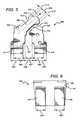
- FIG. 7depicts a partially transparent side view of the surface mount device 100 .
- the second lead element 108is shown extending through the first surface 109 of the casing 101 and is bent 703 to be positioned along the first surface 109 .
- the second lead element 108terminates at a point 710 that is about equal to an end 706 of the first surface 109 and/or the casing 101 .
- the second lead element 108is shown with a termination thickness 702 that is greater than the interior thickness 202 of the portion of the second lead element 107 encased in the casing 101 .
- the second lead element 108may attain an initial external thickness 701 after being bent 703 , and the termination thickness 702 at the termination 710 of the lead element.
- the external thickness 701can be about equal with the termination thickness 702 ; however, in some instances, the lead can continue to increase in thickness as it extends from the bend 703 and along the first surface 109 of the casing to the termination 710 having the termination thickness 702 that is greater than the initial external thickness 701 .
- the first lead element 107can be similarly configured with a thickness exterior to the casing that is greater than a thickness of the portion encased in the casing. The thicknesses can depend on the size and shape of the surface mount device 100 , the surface to be mounted on, the shape of the casing 101 and/or anticipated use.
- the casing 101is generally cubicle and the end 706 of the casing 101 is substantially flat or level. Additionally or alternatively, the casing 101 comprises first and second leg portions 704 and 705 .
- the lead elements 107 and 108terminate 710 , in some implementations, prior to the end 706 of the casing 101 . In other implementations, the termination 710 of the lead elements 107 and 108 is substantially level with the end 706 of the first and second legs 704 and 705 .
- FIG. 8generally depicts a partially transparent, side view of the surface mount device 100 mounted and/or coupled, for example, to a circuit board 801 .
- the first and second lead elements 107 and 108exit the casing 101 through the first surface 109 , allowing for a side mount installation.
- the surface mount device 100can emit and/or receive light through the recess 110 in the second surface 120 .
- the second lead element 108is coupled to a solder pad 802 formed on the circuit board 801 .
- the first lead element 107(not shown in FIG. 8 ) can similarly be coupled or bonded with the circuit board 801 , where the first lead element 107 is coupled to a separate solder pad (not shown) that is electrically isolated or insulated from the solder pad 802 coupled with the second lead element 108 .
- Some embodimentsprovide surface mount devices that at least in part improve the stability and positioning of the lead elements 107 and 108 and the electronic element 302 within the surface mount device through the configuration and design of the lead frame system 200 . In some embodiments, this is accomplished, in part by increasing exposed and/or adhesion areas of casing material around the lead elements 107 and 108 through the implementation and configuration of the first and/or second indentations or vacant areas 103 , 105 extending from within the casing and into the area exposed by the recess 110 .
- the first and/or second lead elements 107 and/or 108can further be configured and/or constructed to additionally draw heat away from the optoelectronic element 302 produced during operation. Typically, the lifetime of an optoelectronic element can be maximized and/or extended by reducing the amount of heat the optoelectronic element absorbs.
- Some embodimentsaugment and/or compensate for the reduced area of the chipset portion 102 due to the first and second indentations 103 and 105 by augmenting other areas of the first lead element 107 .
- the overall area of first lead element 107may be compensated by increasing the widths 501 , 503 , 601 of the first lead element 107 (and/or second lead element 108 ), termination end 210 , head portion 106 , and/or other areas.
- the lead elements 107 and 108can be configured with thicknesses (e.g., external thicknesses 701 , 702 ) that increase the overall volume and/or area of the lead elements and in part maintain or increase the capacity of the first and/or second lead elements ability to absorb and draw heat away from the optoelectronic element.
- Increasing the thickness 702 of the lead elements 107 and 108may also facilitate and/or enhance the coupling of the surface mount device 100 to a circuit board.
- the external thicknesses 701 and/or 702 of the lead elements 107 and 108can be greater than 0.10 mm, typically greater than 0.15 mm, and often increased to 0.3 mm or more.
- FIG. 9depicts a perspective view of the surface mount device package 100 of FIG. 1 as viewed from the end 706 opposite the second surface 120 showing the first and second lead elements 107 and 108 extending through the first surface 109 of the casing 101 and bent along the first surface 109 .
- the first lead element 107maintains a first width 601 outside of the casing 101
- the second lead element 108maintains a second width 602 outside of the casing.
- the first and second lead elements 107 and 108at least terminate with the termination second thickness 702 .
- FIG. 10depicts a flow diagram of a process 1020 for use in manufacturing a surface mount device 100 according to some embodiments.
- a first lead element 107 with a chipset portion 102is shaped.
- the chipset portion 102is electrically secured with the external coupling portion 450 .
- the chipset portionmay, in part, be shaped to couple to, and in some instances support, an optoelectronic element.
- the second lead element 108is shaped.
- the shaping of the first and/or second lead elements 107 and 108can be achieved through metal stamping, injection molding, cutting, etching or through other methods and/or combinations of methods.
- the shaping of the first lead elementmay include shaping the chipset portion in a generally triangular shape, and defining one or more vacant areas as indentations in one or more edges of the chipset portion.
- steps 1022 and 1024are preformed simultaneously. For example, if the first and second lead elements 107 and 108 are metal stamped (e.g., stamped simultaneously from a single sheet of relevant material).
- the casing 101is formed and/or secured with the first and second lead elements 107 and 108 .
- the casingis formed through an injection molding process molding the casing in the desired shape about the first and second lead elements.
- the casingcan be shaped to fit with the lead elements and then secured with the lead elements through adhesive, friction fits, pegs and slots, and other relevant methods.
- the recess 110is formed and/or the chipset portion 102 is cleared and exposed such that portions of the first and second indentations 103 , 105 extend into and are exposed through the recess 110 .
- the recessmay be formed while molding.
- the chipset portionmay include some residual casing material and/or other stray material. This residual or stray material is removed in step 1030 . In other embodiments, the recess is cut, etched or otherwise formed through the second surface 120 of the casing 101 .
- the process 1020includes an optional step 1032 where the first and second lead elements are separated from a support structure and/or sheet of metal.
- the first and second leadsmay not be fully separated to allow for easy of handling of the leads and/or to increase production by mass processing multiple surface mount devices 100 at a time.
- step 1034the portions of the first and second lead elements 107 and 108 exiting the casing 101 are bent along the first surface 109 of the casing.
- step optional 1036the ends of the first and second lead elements 107 and 108 are cut when needed such that the ends of the first and second lead elements terminate at about the end 706 of the casing.
- the first and second leadsare initially cut or formed with lengths to closely or precisely align with the end 706 of the casing.
- the process 1020can include steps of forming a top portion of the casing and a bottom portion of the casing.
- Step 1026can instead provide for the top and bottom portions to be secured together about the first and second lead elements 107 and 108 , such as with pegs extending from the bottom portion through the one or more indentations and/or vacant areas of the lead elements to mate with bores or slots in the top portion.
- Other stepscan additionally and/or alternatively be employed in manufacturing surface mount devices according to some embodiments.
Landscapes
- Engineering & Computer Science (AREA)
- Microelectronics & Electronic Packaging (AREA)
- Led Device Packages (AREA)
- Piezo-Electric Or Mechanical Vibrators, Or Delay Or Filter Circuits (AREA)
- Casings For Electric Apparatus (AREA)
Abstract
Description
Claims (32)
Priority Applications (1)
| Application Number | Priority Date | Filing Date | Title |
|---|---|---|---|
| US12/695,978US9035439B2 (en) | 2006-03-28 | 2010-01-28 | Apparatus, system and method for use in mounting electronic elements |
Applications Claiming Priority (2)
| Application Number | Priority Date | Filing Date | Title |
|---|---|---|---|
| US11/277,717US7675145B2 (en) | 2006-03-28 | 2006-03-28 | Apparatus, system and method for use in mounting electronic elements |
| US12/695,978US9035439B2 (en) | 2006-03-28 | 2010-01-28 | Apparatus, system and method for use in mounting electronic elements |
Related Parent Applications (1)
| Application Number | Title | Priority Date | Filing Date |
|---|---|---|---|
| US11/277,717DivisionUS7675145B2 (en) | 2006-03-28 | 2006-03-28 | Apparatus, system and method for use in mounting electronic elements |
Publications (2)
| Publication Number | Publication Date |
|---|---|
| US20100133002A1 US20100133002A1 (en) | 2010-06-03 |
| US9035439B2true US9035439B2 (en) | 2015-05-19 |
Family
ID=38574337
Family Applications (2)
| Application Number | Title | Priority Date | Filing Date |
|---|---|---|---|
| US11/277,717Active2027-11-10US7675145B2 (en) | 2006-03-28 | 2006-03-28 | Apparatus, system and method for use in mounting electronic elements |
| US12/695,978ActiveUS9035439B2 (en) | 2006-03-28 | 2010-01-28 | Apparatus, system and method for use in mounting electronic elements |
Family Applications Before (1)
| Application Number | Title | Priority Date | Filing Date |
|---|---|---|---|
| US11/277,717Active2027-11-10US7675145B2 (en) | 2006-03-28 | 2006-03-28 | Apparatus, system and method for use in mounting electronic elements |
Country Status (3)
| Country | Link |
|---|---|
| US (2) | US7675145B2 (en) |
| CN (2) | CN102137573B (en) |
| WO (1) | WO2007141664A2 (en) |
Cited By (4)
| Publication number | Priority date | Publication date | Assignee | Title |
|---|---|---|---|---|
| US20150001575A1 (en)* | 2008-07-23 | 2015-01-01 | Rohm Co., Ltd. | Led module |
| US20170104070A1 (en)* | 2015-10-08 | 2017-04-13 | United Microelectronics Corp. | Semiconductor device and method for fabricating the same |
| US10256385B2 (en) | 2007-10-31 | 2019-04-09 | Cree, Inc. | Light emitting die (LED) packages and related methods |
| US20190222171A1 (en)* | 2018-01-18 | 2019-07-18 | Zhejiang Renhe Photovoltaic Technology Co., Ltd | Electrically conductive module of solar cell terminal box |
Families Citing this family (31)
| Publication number | Priority date | Publication date | Assignee | Title |
|---|---|---|---|---|
| US20080246397A1 (en)* | 2007-04-04 | 2008-10-09 | Bily Wang | Manufacturing method of white light led and structure thereof |
| JP4683053B2 (en)* | 2008-01-28 | 2011-05-11 | 日亜化学工業株式会社 | Injection mold, semiconductor package molded by the same, and method of manufacturing semiconductor package |
| DE102008048259B4 (en)* | 2008-09-22 | 2024-10-02 | OSRAM Opto Semiconductors Gesellschaft mit beschränkter Haftung | Housing for an optoelectronic component, side-emitting component with a housing and method for producing a housing |
| US10431567B2 (en) | 2010-11-03 | 2019-10-01 | Cree, Inc. | White ceramic LED package |
| US8101955B2 (en)* | 2009-04-17 | 2012-01-24 | Avago Technologies Ecbu Ip (Singapore) Pte. Ltd. | PLCC package with a reflector cup surrounded by an encapsulant |
| US8089075B2 (en)* | 2009-04-17 | 2012-01-03 | Avago Technologies Ecbu Ip (Singapore) Pte. Ltd. | LFCC package with a reflector cup surrounded by a single encapsulant |
| JPWO2010134647A1 (en)* | 2009-05-22 | 2012-11-12 | Necネットワークプロダクツ株式会社 | Reflector device and parabolic antenna using the same |
| US8101962B2 (en)* | 2009-10-06 | 2012-01-24 | Kuang Hong Precision Co., Ltd. | Carrying structure of semiconductor |
| USD624884S1 (en)* | 2009-10-26 | 2010-10-05 | Foxsemicon Integrated Technology, Inc. | Light emitting diode |
| USD622232S1 (en)* | 2009-10-26 | 2010-08-24 | Foxsemicon Integrated Technology, Inc. | Light emitting diode |
| USD651183S1 (en)* | 2010-02-01 | 2011-12-27 | Foxsemicon Integrated Technology, Inc. | Light-emitting diode |
| USD627314S1 (en)* | 2010-02-01 | 2010-11-16 | Foxsemicon Integrated Technology, Inc. | Light-emitting diode |
| USD627313S1 (en)* | 2010-02-01 | 2010-11-16 | Foxsemicon Integrated Technology, Inc. | Light-emitting diode |
| USD627311S1 (en)* | 2010-02-01 | 2010-11-16 | Foxsemicon Integrated Technology, Inc. | Light-emitting diode |
| USD627312S1 (en)* | 2010-02-01 | 2010-11-16 | Foxsemicon Integrated Technology, Inc. | Light-emitting diode |
| US8178961B2 (en)* | 2010-04-27 | 2012-05-15 | Advanced Semiconductor Engineering, Inc. | Semiconductor package structure and package process |
| US9831393B2 (en)* | 2010-07-30 | 2017-11-28 | Cree Hong Kong Limited | Water resistant surface mount device package |
| USD665366S1 (en)* | 2011-08-12 | 2012-08-14 | Silitek Electronic (Guangzhou) Co., Ltd. | Package carrier |
| USD665367S1 (en)* | 2011-08-12 | 2012-08-14 | Silitek Electronic (Guangzhou) Co., Ltd. | Package carrier |
| USD664938S1 (en)* | 2011-08-12 | 2012-08-07 | Silitek Electronic (Guangzhou) Co., Ltd. | Package carrier |
| USD664939S1 (en)* | 2011-08-12 | 2012-08-07 | Silitek Electronic (Guangzhou) Co., Ltd. | Package carrier |
| USD664509S1 (en)* | 2011-08-12 | 2012-07-31 | Silitek Electronic (Guangzhou) Co., Ltd. | Package carrier |
| JP6102187B2 (en)* | 2012-10-31 | 2017-03-29 | 日亜化学工業株式会社 | Light emitting device package and light emitting device using the same |
| JP6107136B2 (en) | 2012-12-29 | 2017-04-05 | 日亜化学工業株式会社 | LIGHT EMITTING DEVICE PACKAGE, LIGHT EMITTING DEVICE INCLUDING THE SAME, AND LIGHTING DEVICE EQUIPPED WITH THE LIGHT EMITTING DEVICE |
| US9711489B2 (en) | 2013-05-29 | 2017-07-18 | Cree Huizhou Solid State Lighting Company Limited | Multiple pixel surface mount device package |
| JP6484396B2 (en) | 2013-06-28 | 2019-03-13 | 日亜化学工業株式会社 | Light emitting device package and light emitting device using the same |
| CN103594604A (en)* | 2013-10-30 | 2014-02-19 | 王定锋 | LED support with electrodes being fully wrapped and packaged, SMD LED lamp and manufacturing method thereof |
| DE102013225552A1 (en) | 2013-12-11 | 2015-06-11 | Osram Opto Semiconductors Gmbh | Optoelectronic component |
| JP6374723B2 (en) | 2014-07-25 | 2018-08-15 | スタンレー電気株式会社 | Semiconductor light emitting device |
| JP1563810S (en)* | 2016-03-24 | 2016-11-21 | ||
| TWI713237B (en)* | 2018-08-01 | 2020-12-11 | 大陸商光寶光電(常州)有限公司 | Led package structure |
Citations (278)
| Publication number | Priority date | Publication date | Assignee | Title |
|---|---|---|---|---|
| US3760237A (en) | 1972-06-21 | 1973-09-18 | Gen Electric | Solid state lamp assembly having conical light director |
| JPS53118019U (en) | 1977-02-28 | 1978-09-20 | ||
| JPS53126570U (en) | 1977-03-15 | 1978-10-07 | ||
| US4307297A (en) | 1978-09-12 | 1981-12-22 | U.S. Philips Corporation | Opto-electronic device |
| US4322735A (en) | 1979-05-11 | 1982-03-30 | Tokyo Shibaura Denki Kabushiki Kaisha | Display device |
| JPS5927559A (en) | 1982-08-07 | 1984-02-14 | Mitsubishi Electric Corp | Semiconductor device package |
| JPS5927559B2 (en) | 1980-05-14 | 1984-07-06 | 株式会社村田製作所 | electroacoustic transformer |
| US4511425A (en) | 1983-06-13 | 1985-04-16 | Dennison Manufacturing Company | Heated pad decorator |
| JPS6148951A (en) | 1984-08-16 | 1986-03-10 | Toshiba Corp | Semiconductor device |
| JPS6148951B2 (en) | 1977-12-09 | 1986-10-27 | Tokyo Shibaura Electric Co | |
| JPS6297156U (en) | 1985-12-09 | 1987-06-20 | ||
| JPS62140758U (en) | 1986-02-28 | 1987-09-05 | ||
| JPS62160564U (en) | 1986-03-31 | 1987-10-13 | ||
| JPH03171780A (en) | 1989-11-30 | 1991-07-25 | Toshiba Lighting & Technol Corp | light emitting diode display element |
| US5042048A (en) | 1990-03-02 | 1991-08-20 | Meyer Brad E | Target illuminators and systems employing same |
| US5040868A (en) | 1989-05-31 | 1991-08-20 | Siemens Aktiengesellschaft | Surface-mountable opto-component |
| US5122943A (en) | 1991-04-15 | 1992-06-16 | Miles Inc. | Encapsulated light emitting diode and method for encapsulation |
| US5130761A (en) | 1990-07-17 | 1992-07-14 | Kabushiki Kaisha Toshiba | Led array with reflector and printed circuit board |
| US5167556A (en) | 1990-07-03 | 1992-12-01 | Siemens Aktiengesellschaft | Method for manufacturing a light emitting diode display means |
| JPH06177424A (en) | 1992-12-03 | 1994-06-24 | Rohm Co Ltd | Light emitting diode lamp and collective type light emitting diode display device |
| US5351106A (en) | 1991-07-01 | 1994-09-27 | Amergraph Corporation | Exposure system |
| JPH07202271A (en) | 1993-12-28 | 1995-08-04 | Matsushita Electric Works Ltd | Light emitting diode and manufacturing method thereof |
| JPH0832120B2 (en) | 1988-05-27 | 1996-03-27 | 松下電器産業株式会社 | Sound field variable device |
| US5703401A (en) | 1995-05-10 | 1997-12-30 | U.S. Philips Corporation | Miniature semiconductor device for surface mounting |
| US5706177A (en) | 1994-12-24 | 1998-01-06 | Temic Telefunken Microelectronic Gmbh | Multi-terminal surface-mounted electronic device |
| JPH10135492A (en) | 1996-10-29 | 1998-05-22 | Citizen Electron Co Ltd | Electronic parts with through hole electrode and its manufacture |
| US5790298A (en) | 1994-05-03 | 1998-08-04 | Gentex Corporation | Method of forming optically transparent seal and seal formed by said method |
| US5813753A (en) | 1997-05-27 | 1998-09-29 | Philips Electronics North America Corporation | UV/blue led-phosphor device with efficient conversion of UV/blues light to visible light |
| JPH10321909A (en) | 1997-05-19 | 1998-12-04 | Nichia Chem Ind Ltd | Semiconductor device |
| JPH118405A (en) | 1997-06-17 | 1999-01-12 | Oki Electric Ind Co Ltd | Light emitting diode array and light emitting diode |
| JPH1154802A (en) | 1997-07-30 | 1999-02-26 | Matsushita Electric Ind Co Ltd | Light emitting device and display device manufactured using the same |
| US5907151A (en) | 1996-05-24 | 1999-05-25 | Siemens Aktiengesellschaft | Surface mountable optoelectronic transducer and method for its production |
| JPH11150306A (en) | 1997-09-12 | 1999-06-02 | Unisplay Sa | Light source and lamp with light source |
| US5942770A (en) | 1997-04-14 | 1999-08-24 | Rohm, Co., Ltd. | Light-emitting diode chip component and a light-emitting device |
| JPH11261113A (en) | 1999-01-14 | 1999-09-24 | Rohm Co Ltd | Surface-mounting luminous equipment |
| US5959316A (en) | 1998-09-01 | 1999-09-28 | Hewlett-Packard Company | Multiple encapsulation of phosphor-LED devices |
| US6061160A (en) | 1996-05-31 | 2000-05-09 | Dowa Mining Co., Ltd. | Component device for optical communication |
| US6066861A (en) | 1996-09-20 | 2000-05-23 | Siemens Aktiengesellschaft | Wavelength-converting casting composition and its use |
| EP1005085A2 (en) | 1998-11-19 | 2000-05-31 | Matsushita Electronics Corporation | Resin-encapsulated electronic device |
| JP2000188358A (en) | 1998-12-22 | 2000-07-04 | Rohm Co Ltd | Semiconductor device |
| JP2000223752A (en) | 1999-01-29 | 2000-08-11 | Nichia Chem Ind Ltd | Optical semiconductor device and its forming method |
| JP2000223751A (en) | 1998-11-25 | 2000-08-11 | Nichia Chem Ind Ltd | Led lamp and display device using the led lamp |
| EP0684648B1 (en) | 1994-05-24 | 2000-09-13 | Sharp Kabushiki Kaisha | Method for producing semiconductor device |
| JP2000261041A (en) | 1999-03-04 | 2000-09-22 | Citizen Electronics Co Ltd | Surface-mounting type light emitting diode and manufacture of the same |
| CN1274906A (en) | 1999-05-24 | 2000-11-29 | 索尼公司 | Two-dimensional display device |
| US6183100B1 (en) | 1997-10-17 | 2001-02-06 | Truck-Lite Co., Inc. | Light emitting diode 360° warning lamp |
| JP2001044506A (en) | 1999-07-26 | 2001-02-16 | Ichikoh Ind Ltd | Light emitting diode fixing structure |
| US6224216B1 (en) | 2000-02-18 | 2001-05-01 | Infocus Corporation | System and method employing LED light sources for a projection display |
| JP2001168400A (en) | 1999-12-09 | 2001-06-22 | Rohm Co Ltd | Chip type light emitting device with case and method of manufacturing the same |
| US6259608B1 (en) | 1999-04-05 | 2001-07-10 | Delphi Technologies, Inc. | Conductor pattern for surface mount devices and method therefor |
| US6274924B1 (en) | 1998-11-05 | 2001-08-14 | Lumileds Lighting, U.S. Llc | Surface mountable LED package |
| JP2001237463A (en) | 2000-02-24 | 2001-08-31 | Matsushita Electric Works Ltd | Led module |
| US6296367B1 (en) | 1999-10-15 | 2001-10-02 | Armament Systems And Procedures, Inc. | Rechargeable flashlight with step-up voltage converter and recharger therefor |
| JP2001518692A (en) | 1997-07-29 | 2001-10-16 | オスラム オプト セミコンダクターズ ゲゼルシャフト ミット ベシュレンクテル ハフツング ウント コンパニー オッフェネ ハンデルスゲゼルシャフト | Photoelectric element |
| JP2002009217A (en) | 2000-06-23 | 2002-01-11 | Fuji Electric Co Ltd | Resin-sealed semiconductor device |
| WO2002017405A1 (en) | 2000-08-23 | 2002-02-28 | Osram Opto Semiconductors Gmbh | Optoelectronic component and method for the production thereof, module and device comprising a module of this type |
| US20020030194A1 (en) | 2000-09-12 | 2002-03-14 | Camras Michael D. | Light emitting diodes with improved light extraction efficiency |
| US6359236B1 (en) | 1992-07-24 | 2002-03-19 | Tessera, Inc. | Mounting component with leads having polymeric strips |
| US20020061174A1 (en) | 2000-01-21 | 2002-05-23 | Hans Hurt | Electro-optical data transfer module |
| US20020066905A1 (en) | 2000-06-20 | 2002-06-06 | Bily Wang | Wing-shaped surface mount package for light emitting diodes |
| CN2498694Y (en) | 2001-08-14 | 2002-07-03 | 北京利亚德电子科技有限公司 | Inclined LED image module |
| JP2002223005A (en) | 2001-01-26 | 2002-08-09 | Toyoda Gosei Co Ltd | Light emitting diode and display device |
| US20020123163A1 (en) | 2000-04-24 | 2002-09-05 | Takehiro Fujii | Edge-emitting light-emitting semiconductor device and method of manufacture thereof |
| US6447124B1 (en) | 1996-03-19 | 2002-09-10 | Donnelly Mirrors Limited | Electro-optic rearview mirror system |
| US6454437B1 (en) | 1999-07-28 | 2002-09-24 | William Kelly | Ring lighting |
| US20020163001A1 (en) | 2001-05-04 | 2002-11-07 | Shaddock David Mulford | Surface mount light emitting device package and fabrication method |
| US6480389B1 (en) | 2002-01-04 | 2002-11-12 | Opto Tech Corporation | Heat dissipation structure for solid-state light emitting device package |
| US20020195935A1 (en) | 1999-12-30 | 2002-12-26 | Harald Jager | Surface-mountable light-emitting diode light source and method of producing a light-emitting diode light source |
| JP2002374005A (en) | 2001-04-10 | 2002-12-26 | Toshiba Corp | Optical semiconductor device |
| US6517218B2 (en) | 2000-03-31 | 2003-02-11 | Relume Corporation | LED integrated heat sink |
| CN2549313Y (en) | 2002-04-17 | 2003-05-07 | 杨英琪 | Building fan night light |
| US20030116769A1 (en) | 2001-12-24 | 2003-06-26 | Samsung Electro-Mechanics Co., Ltd. | Light emission diode package |
| US6610563B1 (en) | 1997-12-15 | 2003-08-26 | Osram Opto Semiconductors Gmbh & Co. Ohg | Surface mounting optoelectronic component and method for producing same |
| US20030160256A1 (en) | 2000-09-01 | 2003-08-28 | General Electric Company | Plastic packaging of LED arrays |
| US6614058B2 (en) | 2001-07-12 | 2003-09-02 | Highlink Technology Corporation | Light emitting semiconductor device with a surface-mounted and flip-chip package structure |
| US6621210B2 (en) | 2000-07-14 | 2003-09-16 | Sony Corporation | Front plate for field-emission display comprising barriers formed of conductive inorganic material |
| JP2003264267A (en) | 2002-03-08 | 2003-09-19 | Rohm Co Ltd | Semiconductor device using semiconductor chip |
| US6624491B2 (en) | 1998-06-30 | 2003-09-23 | Osram Opto Semiconductors Gmbh & Co. | Diode housing |
| US20030183852A1 (en) | 2002-03-20 | 2003-10-02 | Sharp Kabushiki Kaisha | Light emitting device and manufacturing method thereof |
| JP2003318449A (en) | 2003-05-20 | 2003-11-07 | Sanyo Electric Co Ltd | Led light source and its fabricating method |
| WO2004003660A1 (en) | 2002-07-01 | 2004-01-08 | Bård Eker Industrial Design As | Projector |
| US6680490B2 (en) | 2001-06-15 | 2004-01-20 | Toyoda Gosei Co., Ltd. | Light-emitting device |
| JP2004022862A (en) | 2002-06-18 | 2004-01-22 | Rohm Co Ltd | Semiconductor device |
| US20040016938A1 (en) | 1996-03-26 | 2004-01-29 | Bruce Baretz | Solid state white light emitter and display using same |
| US6686609B1 (en) | 2002-10-01 | 2004-02-03 | Ultrastar Limited | Package structure of surface mounting led and method of manufacturing the same |
| JP2004056075A (en) | 2002-05-31 | 2004-02-19 | Stanley Electric Co Ltd | Light emitting device and manufacturing method thereof |
| US20040037076A1 (en) | 2002-07-17 | 2004-02-26 | Sharp Kabushiki Kaisha | Light emitting diode lamp and light emitting diode display unit |
| US6700136B2 (en) | 2001-07-30 | 2004-03-02 | General Electric Company | Light emitting device package |
| US20040041222A1 (en) | 2002-09-04 | 2004-03-04 | Loh Ban P. | Power surface mount light emitting die package |
| US6710373B2 (en) | 1999-09-27 | 2004-03-23 | Shih-Yi Wang | Means for mounting photoelectric sensing elements, light emitting diodes, or the like |
| JP2004103775A (en) | 2002-09-09 | 2004-04-02 | Eeshikku Kk | Chip led light emitting body and method for manufacturing the same |
| US6717353B1 (en) | 2002-10-14 | 2004-04-06 | Lumileds Lighting U.S., Llc | Phosphor converted light emitting device |
| JP2004111937A (en) | 2002-08-30 | 2004-04-08 | Nichia Chem Ind Ltd | Light emitting device |
| WO2003049204A3 (en) | 2001-11-30 | 2004-04-29 | Osram Opto Semiconductors Gmbh | Optoelectronic component |
| WO2004036660A1 (en) | 2002-09-02 | 2004-04-29 | Tco Co., Ltd | A surface mounting type light emitting diode |
| US20040079957A1 (en) | 2002-09-04 | 2004-04-29 | Andrews Peter Scott | Power surface mount light emitting die package |
| US20040080939A1 (en) | 2001-04-23 | 2004-04-29 | Jules Braddell | Illuminator |
| EP1418630A1 (en) | 2002-11-07 | 2004-05-12 | Matsushita Electric Industrial Co., Ltd. | LED lamp |
| US20040090174A1 (en) | 2000-12-28 | 2004-05-13 | Stefan Tasch | Light source comprising a light-emitting element |
| CN2617039Y (en) | 2003-02-21 | 2004-05-19 | 游尚桦 | Adhesive LED lead frame |
| JP2004146815A (en) | 2002-09-30 | 2004-05-20 | Sanyo Electric Co Ltd | Light emitting device |
| WO2004053933A2 (en) | 2002-12-06 | 2004-06-24 | Cree, Inc. | Composite leadframe led package and method of making the same |
| JP2004200236A (en) | 2002-12-16 | 2004-07-15 | Matsushita Electric Ind Co Ltd | Light emitting diode display |
| US6765235B2 (en) | 2002-02-27 | 2004-07-20 | Oki Data Corporation | Array of semiconductor elements with paired driving scheme |
| US6770498B2 (en) | 2002-06-26 | 2004-08-03 | Lingsen Precision Industries, Ltd. | LED package and the process making the same |
| US6774401B2 (en) | 2002-07-12 | 2004-08-10 | Stanley Electric Co., Ltd. | Light emitting diode |
| JP2004228387A (en) | 2003-01-23 | 2004-08-12 | Koha Co Ltd | Light emitting device |
| US6791259B1 (en) | 1998-11-30 | 2004-09-14 | General Electric Company | Solid state illumination system containing a light emitting diode, a light scattering material and a luminescent material |
| CN2646873Y (en) | 2003-10-16 | 2004-10-06 | 上海三思科技发展有限公司 | A surface sticking type LED with tilted light axis |
| US20040217364A1 (en) | 2003-05-01 | 2004-11-04 | Cree Lighting Company, Inc. | Multiple component solid state white light |
| JP2004327955A (en) | 2003-04-09 | 2004-11-18 | Citizen Electronics Co Ltd | LED lamp |
| US20040227149A1 (en) | 2003-04-30 | 2004-11-18 | Cree, Inc. | High powered light emitter packages with compact optics |
| JP2004335740A (en) | 2003-05-07 | 2004-11-25 | Citizen Electronics Co Ltd | Light emitting diode and its package structure |
| JP2004335880A (en) | 2003-05-09 | 2004-11-25 | Toshiba Lighting & Technology Corp | Light emitting device |
| US20040232435A1 (en) | 2003-02-28 | 2004-11-25 | Osram Opto Semiconductors Gmbh | Optoelectronic device with patterned-metallized package body, method for producing such a device and method for the patterned metallization of a plastic-containing body |
| WO2004044877A3 (en) | 2002-11-11 | 2004-12-02 | Cotco Internat Ltd | A display device and method for making same |
| JP2004342870A (en) | 2003-05-16 | 2004-12-02 | Stanley Electric Co Ltd | Light emitting diode for driving large current |
| US20040256706A1 (en) | 2003-06-20 | 2004-12-23 | Shintaro Nakashima | Molded package and semiconductor device using molded package |
| JP2005019838A (en) | 2003-06-27 | 2005-01-20 | Nippon Leiz Co Ltd | Light source device and method for manufacturing the same |
| US20050023548A1 (en) | 2003-07-31 | 2005-02-03 | Bhat Jerome C. | Mount for semiconductor light emitting device |
| CN1581527A (en) | 2003-08-13 | 2005-02-16 | 西铁城电子股份有限公司 | Luminous diode |
| CN1591924A (en) | 2003-07-29 | 2005-03-09 | 西铁城电子股份有限公司 | Surface-mounted LED and light emitting device with same |
| JP2005079167A (en) | 2003-08-28 | 2005-03-24 | Kyocera Corp | Light emitting element storage package and light emitting device |
| US6872585B2 (en) | 2001-09-03 | 2005-03-29 | Toyoda Gosei Co., Ltd. | LED device and manufacturing method thereof |
| US6876149B2 (en) | 2002-01-31 | 2005-04-05 | Citizen Electronics Co., Ltd. | Double-face LED device for an electronic instrument |
| EP1521313A2 (en) | 2003-10-03 | 2005-04-06 | LumiLeds Lighting U.S., LLC | Integrated reflector cup for a light emitting device mount |
| US20050072981A1 (en) | 2002-02-19 | 2005-04-07 | Ryoma Suenaga | Light-emitting device and process for producing thereof |
| US20050077535A1 (en) | 2003-10-08 | 2005-04-14 | Joinscan Electronics Co., Ltd | LED and its manufacturing process |
| US20050093005A1 (en) | 2002-06-28 | 2005-05-05 | Osram Opto Semiconductors Gmbh | Optoelectronic component and method for producing it |
| US20050110033A1 (en) | 1998-07-28 | 2005-05-26 | Paul Heremans | High-efficiency radiating device |
| US20050117320A1 (en) | 2003-11-14 | 2005-06-02 | Hon Hai Precision Industry Co., Ltd. | Light-emitting diode and backlight system using the same |
| EP1538680A2 (en) | 2003-12-03 | 2005-06-08 | Sumitomo Electric Industries, Ltd. | Light emitting device |
| JP2005150624A (en) | 2003-11-19 | 2005-06-09 | Matsushita Electric Ind Co Ltd | Lead frame for semiconductor device and surface light emitting device using the same |
| US20050135105A1 (en) | 2003-12-19 | 2005-06-23 | Lumileds Lighting U.S., Llc | LED package assembly |
| US6911678B2 (en) | 2003-05-30 | 2005-06-28 | Stanley Electric Co., Ltd. | Glass-sealed light-emitting diode |
| US20050152127A1 (en) | 2003-12-19 | 2005-07-14 | Takayuki Kamiya | LED lamp apparatus |
| US20050156187A1 (en) | 2002-03-08 | 2005-07-21 | Shinji Isokawa | Semiconductor device using semiconductor chip |
| US20050179376A1 (en) | 2004-02-13 | 2005-08-18 | Fung Elizabeth C.L. | Light emitting diode display device |
| US20050179041A1 (en) | 2004-02-18 | 2005-08-18 | Lumileds Lighting U.S., Llc | Illumination system with LEDs |
| JP2005223222A (en) | 2004-02-06 | 2005-08-18 | Toyoda Gosei Co Ltd | Solid element package |
| JP2003324214A5 (en) | 2002-04-30 | 2005-08-25 | ||
| US6940704B2 (en) | 2001-01-24 | 2005-09-06 | Gelcore, Llc | Semiconductor light emitting device |
| US20050199899A1 (en) | 2004-03-11 | 2005-09-15 | Ming-Der Lin | Package array and package unit of flip chip LED |
| JP2005259754A (en) | 2004-03-09 | 2005-09-22 | Korai Kagi Kofun Yugenkoshi | Light emitting diode device capable of preventing electrostatic discharge damage |
| JP2005259972A (en) | 2004-03-11 | 2005-09-22 | Stanley Electric Co Ltd | Surface mount type LED |
| US20050231983A1 (en) | 2002-08-23 | 2005-10-20 | Dahm Jonathan S | Method and apparatus for using light emitting diodes |
| WO2005104247A1 (en) | 2004-04-19 | 2005-11-03 | Matsushita Electric Industrial Co., Ltd. | Method for fabricating led illumination light source and led illumination light source |
| JP2005310935A (en) | 2004-04-20 | 2005-11-04 | Sumitomo Metal Electronics Devices Inc | Storing package for light-emitting element |
| US6964877B2 (en) | 2003-03-28 | 2005-11-15 | Gelcore, Llc | LED power package |
| US20050253130A1 (en) | 2004-03-26 | 2005-11-17 | Koito Manufacturing Co., Ltd. | Light source module and vehicle front lamp |
| US6975011B2 (en) | 1995-09-29 | 2005-12-13 | Osram Gmbh | Optoelectronic semiconductor component having multiple external connections |
| JP2005347401A (en) | 2004-06-01 | 2005-12-15 | Meiko:Kk | Optical element chip component |
| JP2005539386A (en) | 2002-09-17 | 2005-12-22 | オスラム オプト セミコンダクターズ ゲゼルシャフト ミット ベシュレンクテル ハフツング | Lead frame based housing, surface mountable photoelectric component and manufacturing method |
| JP2006019557A (en) | 2004-07-02 | 2006-01-19 | Fujikura Ltd | LIGHT EMITTING DEVICE AND ITS MOUNTING METHOD, LIGHTING APPARATUS AND DISPLAY |
| US6995510B2 (en) | 2001-12-07 | 2006-02-07 | Hitachi Cable, Ltd. | Light-emitting unit and method for producing same as well as lead frame used for producing light-emitting unit |
| WO2006016398A1 (en) | 2004-08-10 | 2006-02-16 | Renesas Technology Corp. | Light emitting device and process for manufacturing the same |
| US7009285B2 (en)* | 2004-03-19 | 2006-03-07 | Lite-On Technology Corporation | Optoelectronic semiconductor component |
| US7009627B2 (en) | 2001-11-21 | 2006-03-07 | Canon Kabushiki Kaisha | Display apparatus, and image signal processing apparatus and drive control apparatus for the same |
| CN1744335A (en) | 2004-08-31 | 2006-03-08 | 斯坦雷电气株式会社 | Surface Mount LEDs |
| JP2006508537A (en) | 2002-11-29 | 2006-03-09 | オスラム オプト セミコンダクターズ ゲゼルシャフト ミット ベシュレンクテル ハフツング | Optoelectronic element |
| USD517025S1 (en) | 2003-03-17 | 2006-03-14 | Nichia Corporation | Light emitting diode |
| US20060060867A1 (en) | 2004-09-09 | 2006-03-23 | Toyoda Gosei Co., Ltd. | Light emitting device |
| US7021797B2 (en) | 2003-05-13 | 2006-04-04 | Light Prescriptions Innovators, Llc | Optical device for repositioning and redistributing an LED's light |
| JP2006108517A (en) | 2004-10-08 | 2006-04-20 | Citizen Watch Co Ltd | Substrate for led connection, illuminator using thereof, and display device using thereof |
| EP1653254A2 (en) | 2004-10-18 | 2006-05-03 | Samsung Electronics Co., Ltd. | Light emitting diode and lens for the same |
| US20060091406A1 (en) | 2004-11-04 | 2006-05-04 | Hiroki Kaneko | Illuminating apparatus, method for fabricating the same and display apparatus using the same |
| JP2006119357A (en) | 2004-10-21 | 2006-05-11 | Koha Co Ltd | Display device |
| GB2420221A (en) | 2004-11-12 | 2006-05-17 | Unity Opto Technology Co Ltd | Semiconductor light emitting diode package with heat sink |
| US20060105478A1 (en) | 2004-11-12 | 2006-05-18 | Lumileds Lighting U.S., Llc | Bonding an optical element to a light emitting device |
| US20060108594A1 (en) | 2004-11-11 | 2006-05-25 | Kazuyuki Iwasaki | LED device and method for manufacturing the same |
| WO2006054228A2 (en) | 2004-11-18 | 2006-05-26 | Koninklijke Philips Electronics N.V. | Illuminator and method for producing such illuminator |
| US7064907B2 (en) | 2003-06-12 | 2006-06-20 | Seiko Epson Corporation | Optical part and its manufacturing method |
| US20060133044A1 (en) | 2004-12-16 | 2006-06-22 | Seoul Semiconductor Co., Ltd. | Leadframe and packaged light emitting diode |
| US20060131591A1 (en) | 2004-12-16 | 2006-06-22 | Naofumi Sumitani | Light emitting apparatus |
| JP2006179520A (en) | 2004-12-20 | 2006-07-06 | Nichia Chem Ind Ltd | Semiconductor device |
| US20060151809A1 (en) | 2003-06-03 | 2006-07-13 | Rohm Co., Ltd | Optical semiconductor unit |
| WO2006046981A3 (en) | 2004-10-25 | 2006-07-13 | Cree Inc | Solid metal block semiconductor light emitting device mounting substrates and packages including cavities and heat sinks, and methods of packaging same |
| EP1693904A2 (en) | 2005-02-18 | 2006-08-23 | Nichia Corporation | Light emitting device provided with lens for controlling light distribution characteristic |
| JP2006253689A (en) | 2005-03-08 | 2006-09-21 | Avago Technologies General Ip (Singapore) Private Ltd | Mounting of LED with high heat dissipation |
| US20060220046A1 (en) | 2005-03-04 | 2006-10-05 | Chuan-Pei Yu | Led |
| US7119422B2 (en) | 2004-11-15 | 2006-10-10 | Unity Opto Technology Co., Ltd. | Solid-state semiconductor light emitting device |
| US20060267042A1 (en) | 2001-10-12 | 2006-11-30 | Nichia Corporation | Light emitting apparatus and method of manufacturing the same |
| JP2006324331A (en) | 2005-05-17 | 2006-11-30 | Sony Corp | Light emitting diode and its manufacturing method, integrated light emitting diode and its manufacturing method, growing method of nitride- based group iii-v compound semiconductor, nitride-based group iii-v compound semiconductor growing substrate, light emitting diode backlight, light emitting diode lighting apparatus, light emitting diode display, and electronic equipment |
| CN1874011A (en) | 2005-06-03 | 2006-12-06 | 邢陈震仑 | A light emitting diode device |
| JP2006332234A (en) | 2005-05-25 | 2006-12-07 | Hitachi Aic Inc | Led device having reflecting function |
| US20060278882A1 (en) | 2005-06-10 | 2006-12-14 | Cree, Inc. | Power lamp package |
| WO2006135502A1 (en) | 2005-06-10 | 2006-12-21 | Cree, Inc. | High power solid-state lamp |
| JP2006344692A (en) | 2005-06-07 | 2006-12-21 | Fujikura Ltd | Light emitting element mounting substrate and light emitting element module |
| US20060291185A1 (en) | 2005-06-28 | 2006-12-28 | Sato Atsushi | Planar light source device and display using the same |
| US7161189B2 (en) | 2004-06-04 | 2007-01-09 | Lite-On Technology Corporation | LED package including a frame |
| CN1913135A (en) | 2005-08-11 | 2007-02-14 | 安华高科技Ecbuip(新加坡)私人有限公司 | PLCC package with integrated lens and method for making the package |
| US20070046176A1 (en) | 2005-04-27 | 2007-03-01 | Spudnik,Inc. | Phosphor Compositions For Scanning Beam Displays |
| US7187009B2 (en) | 2001-06-12 | 2007-03-06 | Citizen Electronics Co., Ltd. | Light emitting diode device for illumination objects |
| EP1187228A4 (en) | 2000-02-09 | 2007-03-07 | Nippon Leiz Corp | LIGHT SOURCE |
| JP2007094088A (en) | 2005-09-29 | 2007-04-12 | Matsushita Electric Ind Co Ltd | Display device |
| JP2007109836A (en) | 2005-10-13 | 2007-04-26 | Fuji Electric Holdings Co Ltd | Printed wiring board |
| US20070096139A1 (en) | 2005-11-02 | 2007-05-03 | 3M Innovative Properties Company | Light emitting diode encapsulation shape control |
| US20070109779A1 (en) | 2005-11-11 | 2007-05-17 | Yoshifumi Sekiguchi | Illuminating device and liquid-crystal display device using the same |
| US7224000B2 (en) | 2002-08-30 | 2007-05-29 | Lumination, Llc | Light emitting diode component |
| CN1977399A (en) | 2005-04-01 | 2007-06-06 | 松下电器产业株式会社 | LED component and method for manufacturing same |
| JP2007165029A (en) | 2005-12-12 | 2007-06-28 | Hitachi Displays Ltd | Display device |
| JP2007165840A (en) | 2005-09-09 | 2007-06-28 | Matsushita Electric Works Ltd | Light-emitting device |
| US20070145401A1 (en) | 2005-12-27 | 2007-06-28 | Sharp Kabushiki Kaisha | Semiconductor light emitting device, semiconductor element, and method for fabricating the semiconductor light emitting device |
| JP2007184542A (en) | 2005-12-09 | 2007-07-19 | Matsushita Electric Ind Co Ltd | LIGHT EMITTING MODULE, ITS MANUFACTURING METHOD, AND BACKLIGHT DEVICE USING THE SAME |
| CN101005109A (en) | 2006-01-16 | 2007-07-25 | 榎本股份有限公司 | Low height lead frame for LED device and the manufacturing method thereof |
| US20070170449A1 (en) | 2006-01-24 | 2007-07-26 | Munisamy Anandan | Color sensor integrated light emitting diode for LED backlight |
| WO2007083408A1 (en) | 2006-01-20 | 2007-07-26 | Sharp Kabushiki Kaisha | Light source unit, lighting apparatus using the light source unit, and display using the lighting apparatus |
| CN101013689A (en) | 2007-01-30 | 2007-08-08 | 深圳市共达光电器件有限公司 | LED packaging structure and packaging method |
| JP2007243226A (en) | 2007-06-20 | 2007-09-20 | Sony Corp | Light source apparatus and display apparatus |
| US7282740B2 (en)* | 2003-12-17 | 2007-10-16 | Sharp Kabushiki Kaisha | Semiconductor light emitting device |
| US7282785B2 (en)* | 2004-01-05 | 2007-10-16 | Stanley Electric Co., Ltd. | Surface mount type semiconductor device and lead frame structure thereof |
| JP2007273763A (en) | 2006-03-31 | 2007-10-18 | Sony Corp | Semiconductor device and its manufacturing method |
| US20070241357A1 (en) | 2004-10-29 | 2007-10-18 | Ledengin, Inc. | LED packages with mushroom shaped lenses and methods of manufacturing LED light-emitting devices |
| US7285802B2 (en) | 2004-12-21 | 2007-10-23 | 3M Innovative Properties Company | Illumination assembly and method of making same |
| WO2007121486A2 (en) | 2006-04-18 | 2007-10-25 | Lamina Lighting, Inc. | Optical devices for controlled color mixing |
| JP2007287981A (en) | 2006-04-18 | 2007-11-01 | Konica Minolta Opto Inc | Light emitting device |
| WO2007122516A2 (en) | 2006-04-26 | 2007-11-01 | Cree Hong Kong Limited | Apparatus and method for use in mounting electronic elements |
| WO2007127029A2 (en) | 2006-04-24 | 2007-11-08 | Cree, Inc. | Side-view surface mount white led |
| US20070262328A1 (en) | 2006-05-10 | 2007-11-15 | Nichia Corporation | Semiconductor light emitting device and a method for producing the same |
| JP2007299905A (en) | 2006-04-28 | 2007-11-15 | Nichia Chem Ind Ltd | Semiconductor device |
| US20070269586A1 (en) | 2006-05-17 | 2007-11-22 | 3M Innovative Properties Company | Method of making light emitting device with silicon-containing composition |
| US7303315B2 (en) | 2004-11-05 | 2007-12-04 | 3M Innovative Properties Company | Illumination assembly using circuitized strips |
| JP2007317896A (en) | 2006-05-26 | 2007-12-06 | Nichia Chem Ind Ltd | Light emitting diode |
| JP2007329516A (en) | 2007-09-14 | 2007-12-20 | Sharp Corp | Semiconductor light emitting device |
| US20070294975A1 (en) | 2006-06-22 | 2007-12-27 | Paul Nadar | Support panel for removable brackets and the like |
| US20070295975A1 (en) | 2004-06-25 | 2007-12-27 | Sanyo Electric Co., Ltd. | Light-Emitting Device |
| US20080013319A1 (en) | 2006-07-13 | 2008-01-17 | Everlight Electronics Co., Ltd. | Light emitting diode package |
| US20080026498A1 (en) | 2006-07-31 | 2008-01-31 | Eric Tarsa | Light emitting diode package element with internal meniscus for bubble free lens placement |
| DE202007012162U1 (en) | 2007-06-05 | 2008-03-20 | Seoul Semiconductor Co., Ltd. | LED housing |
| US20080093606A1 (en) | 2006-10-24 | 2008-04-24 | Chipmos Technologies Inc. | Light emitting chip package and manufacturing method thereof |
| US20080121921A1 (en) | 2006-07-13 | 2008-05-29 | Cree, Inc. | Leadframe-based packages for solid state light emitting devices and methods of forming leadframe-based packages for solid state light emitting devices |
| US20080149960A1 (en) | 2006-12-26 | 2008-06-26 | Nichia Corporation | Light-emitting apparatus and method of producing the same |
| USD572210S1 (en) | 2006-11-01 | 2008-07-01 | Lg Innotek Co., Ltd. | Light-emitting diode (LED) |
| USD572670S1 (en) | 2006-03-30 | 2008-07-08 | Nichia Corporation | Light emitting diode |
| WO2008081794A1 (en) | 2006-12-28 | 2008-07-10 | Nichia Corporation | Light emitting device and method for manufacturing the same |
| WO2008082098A1 (en) | 2006-12-28 | 2008-07-10 | Seoul Semiconductor Co., Ltd. | Light emitting diode package |
| US20080170391A1 (en) | 2007-01-12 | 2008-07-17 | Aizar Abdul Karim Norfidathul | Multi-chip Packaged LED Light Source |
| EP1953834A1 (en) | 2005-11-21 | 2008-08-06 | Matsushita Electric Works, Ltd. | Light-emitting device |
| US20080191232A1 (en) | 2005-08-01 | 2008-08-14 | Seoul Semiconductor Co., Ltd. | Light Emitting Device With A Lens Of Silicone |
| US20080198594A1 (en) | 2006-12-19 | 2008-08-21 | Lee Sungkeun | Optical module |
| USD576574S1 (en) | 2007-07-17 | 2008-09-09 | Rohm Co., Ltd. | Light emitting diode module |
| US20080230790A1 (en) | 2007-03-23 | 2008-09-25 | Sharp Kabushiki Kaisha | Semiconductor light emitting device |
| US7429757B2 (en) | 2002-06-19 | 2008-09-30 | Sanken Electric Co., Ltd. | Semiconductor light emitting device capable of increasing its brightness |
| US7436002B2 (en)* | 2001-06-29 | 2008-10-14 | Osram Gmbh | Surface-mountable radiation-emitting component |
| US20080258156A1 (en) | 2006-09-29 | 2008-10-23 | Sanyo Electric Co., Ltd. | Light-emitting diode apparatus |
| US20080296590A1 (en) | 2007-05-31 | 2008-12-04 | Kee Yean Ng | LED-Based Light Source Having Improved Thermal Dissipation |
| US20080303052A1 (en) | 2004-09-10 | 2008-12-11 | Seoul Semiconductor Co., Ltd. | Light emitting diode package having multiple molding resins |
| US20080308825A1 (en) | 2007-06-14 | 2008-12-18 | Cree, Inc. | Encapsulant with scatterer to tailor spatial emission pattern and color uniformity in light emitting diodes |
| CN101360368A (en) | 2007-07-30 | 2009-02-04 | 深圳莱特光电有限公司 | Silver layer insulation method in warm white light LED encapsulation process |
| US20090050908A1 (en) | 2005-01-10 | 2009-02-26 | Cree, Inc. | Solid state lighting component |
| US20090050911A1 (en) | 2007-08-24 | 2009-02-26 | Cree, Inc. | Light emitting device packages using light scattering particles of different size |
| US20090057708A1 (en) | 2007-08-27 | 2009-03-05 | Norfidathul Aizar Abdul Karim | LED Light Source Having Improved Resistance to Thermal Cycling |
| US20090057699A1 (en) | 2007-09-04 | 2009-03-05 | Philips Lumileds Lighting Company, Llc | LED with Particles in Encapsulant for Increased Light Extraction and Non-Yellow Off-State Color |
| US20090072251A1 (en) | 2007-09-14 | 2009-03-19 | Cotco Luminant Device Limited | LED surface-mount device and LED display incorporating such device |
| US20090095966A1 (en) | 2007-10-10 | 2009-04-16 | Cree, Inc. | Multiple conversion material light emitting diode package and method of fabricating same |
| US20090129085A1 (en) | 2007-11-16 | 2009-05-21 | Avago Technologies Ecbu Ip (Singapore) Pte. Ltd. | Optical device |
| WO2009074919A1 (en) | 2007-12-11 | 2009-06-18 | Koninklijke Philips Electronics N.V. | Side emitting device with hybrid top reflector |
| US20090189178A1 (en) | 2006-06-30 | 2009-07-30 | Do Hyung Kim | Leadframe having a heat sink supporting part, fabricating method of a light emitting diode package using the same, and light emitting diode package fabricated by the method |
| US7579628B2 (en) | 2004-10-18 | 2009-08-25 | Sharp Kabushiki Kaisha | Backlight device for liquid crystal display including a plurality of light emitting diodes within their own concaves aligned in a straight line within a larger concave |
| GB2458972A (en) | 2008-08-05 | 2009-10-07 | Photonstar Led Ltd | Thermally optimized chip-on-board module |
| US20090283781A1 (en) | 2008-05-16 | 2009-11-19 | Cree Hong Kong Limited | Mini V SMD |
| US7622795B2 (en) | 2007-05-15 | 2009-11-24 | Nichepac Technology Inc. | Light emitting diode package |
| WO2010005294A1 (en) | 2008-06-15 | 2010-01-14 | Stichting Administratiekantoor Vomgroup | A method for manufacturing a lens to be added to a led, and a lens obtained with that method |
| US20100044735A1 (en) | 2008-08-25 | 2010-02-25 | Citizen Electronics Co., Ltd. | Light-emitting device |
| US20100103660A1 (en) | 2008-10-24 | 2010-04-29 | Cree Led Lighting Solutions, Inc. | Array layout for color mixing |
| EP1864780B1 (en) | 2006-06-09 | 2010-05-26 | LG Electronics Inc. | Apparatus and method for manufacturing a light emitting unit |
| GB2466633A (en) | 2008-12-12 | 2010-07-07 | Glory Science Co Ltd | Method of manufacturing a light emitting unit |
| US20100193822A1 (en) | 2009-01-30 | 2010-08-05 | Nichia Corporation | Light emitting semiconductor device and method of manufacture thereof |
| US7777412B2 (en) | 2007-03-22 | 2010-08-17 | Avago Technologies Ecbu Ip (Singapore) Pte. Ltd. | Phosphor converted LED with improved uniformity and having lower phosphor requirements |
| US7875899B2 (en) | 2007-01-15 | 2011-01-25 | Showa Denko K.K. | Light-emitting diode package and lead group structure for light-emitting diode package |
| US20110049545A1 (en) | 2009-09-02 | 2011-03-03 | Koninklijke Philips Electronics N.V. | Led package with phosphor plate and reflective substrate |
| US20110108874A1 (en) | 2009-11-05 | 2011-05-12 | Luminit, Llc | Method to Provide Microstructure for Encapsulated Hgh-Brightness LED Chips |
| US20110186880A1 (en) | 2007-08-30 | 2011-08-04 | Osram Opto Semiconductors Gmbh | LED Housing |
| US20110193118A1 (en) | 2010-02-09 | 2011-08-11 | Oshima Yukitoyo | Light emitting device and manufacturing method thereof |
| US20110278617A1 (en) | 2010-05-12 | 2011-11-17 | Lee Gun Kyo | Light emitting device package |
| US8217414B2 (en) | 2006-12-28 | 2012-07-10 | Nichia Corporation | Light emitting device, package, light emitting device manufacturing method, package manufacturing method and package manufacturing die |
| US20120257386A1 (en) | 2011-06-24 | 2012-10-11 | Xicato, Inc. | Led based illumination module with a reflective mask |
| EP1187226B1 (en) | 2000-09-01 | 2012-12-26 | Citizen Electronics Co., Ltd. | Surface-mount type light emitting diode and method of manufacturing same |
Family Cites Families (4)
| Publication number | Priority date | Publication date | Assignee | Title |
|---|---|---|---|---|
| JPH08139257A (en) | 1994-11-07 | 1996-05-31 | Hitachi Ltd | Surface mount semiconductor device |
| US6718626B2 (en)* | 2000-09-13 | 2004-04-13 | Fuji Machine Mfg. Co., Ltd. | Apparatus for detecting positioning error of a component with respect to a suction nozzle |
| JP2003324214A (en) | 2002-04-30 | 2003-11-14 | Omron Corp | Light emitting module |
| US8214114B2 (en)* | 2007-11-04 | 2012-07-03 | GM Global Technology Operations LLC | Control of engine torque for traction and stability control events for a hybrid powertrain system |
- 2006
- 2006-03-28USUS11/277,717patent/US7675145B2/enactiveActive
- 2007
- 2007-03-27WOPCT/IB2007/002432patent/WO2007141664A2/enactiveApplication Filing
- 2007-03-27CNCN201110039138.9Apatent/CN102137573B/ennot_activeExpired - Fee Related
- 2007-03-27CNCN2007800196439Apatent/CN101454911B/enactiveActive
- 2010
- 2010-01-28USUS12/695,978patent/US9035439B2/enactiveActive
Patent Citations (328)
| Publication number | Priority date | Publication date | Assignee | Title |
|---|---|---|---|---|
| US3760237A (en) | 1972-06-21 | 1973-09-18 | Gen Electric | Solid state lamp assembly having conical light director |
| JPS53118019U (en) | 1977-02-28 | 1978-09-20 | ||
| JPS53126570U (en) | 1977-03-15 | 1978-10-07 | ||
| JPS6148951B2 (en) | 1977-12-09 | 1986-10-27 | Tokyo Shibaura Electric Co | |
| US4307297A (en) | 1978-09-12 | 1981-12-22 | U.S. Philips Corporation | Opto-electronic device |
| US4322735A (en) | 1979-05-11 | 1982-03-30 | Tokyo Shibaura Denki Kabushiki Kaisha | Display device |
| JPS5927559B2 (en) | 1980-05-14 | 1984-07-06 | 株式会社村田製作所 | electroacoustic transformer |
| JPS5927559A (en) | 1982-08-07 | 1984-02-14 | Mitsubishi Electric Corp | Semiconductor device package |
| US4511425A (en) | 1983-06-13 | 1985-04-16 | Dennison Manufacturing Company | Heated pad decorator |
| JPS6148951A (en) | 1984-08-16 | 1986-03-10 | Toshiba Corp | Semiconductor device |
| JPS6297156U (en) | 1985-12-09 | 1987-06-20 | ||
| JPS62140758U (en) | 1986-02-28 | 1987-09-05 | ||
| JPS62160564U (en) | 1986-03-31 | 1987-10-13 | ||
| JPH0832120B2 (en) | 1988-05-27 | 1996-03-27 | 松下電器産業株式会社 | Sound field variable device |
| US5040868A (en) | 1989-05-31 | 1991-08-20 | Siemens Aktiengesellschaft | Surface-mountable opto-component |
| EP1187227A3 (en) | 1989-05-31 | 2002-08-28 | Osram Opto Semiconductors GmbH & Co. OHG | Surface-mountable optical element and method of fabrication |
| JPH03171780A (en) | 1989-11-30 | 1991-07-25 | Toshiba Lighting & Technol Corp | light emitting diode display element |
| US5042048A (en) | 1990-03-02 | 1991-08-20 | Meyer Brad E | Target illuminators and systems employing same |
| US5167556A (en) | 1990-07-03 | 1992-12-01 | Siemens Aktiengesellschaft | Method for manufacturing a light emitting diode display means |
| US5130761A (en) | 1990-07-17 | 1992-07-14 | Kabushiki Kaisha Toshiba | Led array with reflector and printed circuit board |
| US5122943A (en) | 1991-04-15 | 1992-06-16 | Miles Inc. | Encapsulated light emitting diode and method for encapsulation |
| US5351106A (en) | 1991-07-01 | 1994-09-27 | Amergraph Corporation | Exposure system |
| US6359236B1 (en) | 1992-07-24 | 2002-03-19 | Tessera, Inc. | Mounting component with leads having polymeric strips |
| JPH06177424A (en) | 1992-12-03 | 1994-06-24 | Rohm Co Ltd | Light emitting diode lamp and collective type light emitting diode display device |
| JPH07202271A (en) | 1993-12-28 | 1995-08-04 | Matsushita Electric Works Ltd | Light emitting diode and manufacturing method thereof |
| US5790298A (en) | 1994-05-03 | 1998-08-04 | Gentex Corporation | Method of forming optically transparent seal and seal formed by said method |
| EP0684648B1 (en) | 1994-05-24 | 2000-09-13 | Sharp Kabushiki Kaisha | Method for producing semiconductor device |
| US5706177A (en) | 1994-12-24 | 1998-01-06 | Temic Telefunken Microelectronic Gmbh | Multi-terminal surface-mounted electronic device |
| US5703401A (en) | 1995-05-10 | 1997-12-30 | U.S. Philips Corporation | Miniature semiconductor device for surface mounting |
| US6975011B2 (en) | 1995-09-29 | 2005-12-13 | Osram Gmbh | Optoelectronic semiconductor component having multiple external connections |
| US6447124B1 (en) | 1996-03-19 | 2002-09-10 | Donnelly Mirrors Limited | Electro-optic rearview mirror system |
| US20040016938A1 (en) | 1996-03-26 | 2004-01-29 | Bruce Baretz | Solid state white light emitter and display using same |
| US5907151A (en) | 1996-05-24 | 1999-05-25 | Siemens Aktiengesellschaft | Surface mountable optoelectronic transducer and method for its production |
| US6061160A (en) | 1996-05-31 | 2000-05-09 | Dowa Mining Co., Ltd. | Component device for optical communication |
| US6066861A (en) | 1996-09-20 | 2000-05-23 | Siemens Aktiengesellschaft | Wavelength-converting casting composition and its use |
| JPH10135492A (en) | 1996-10-29 | 1998-05-22 | Citizen Electron Co Ltd | Electronic parts with through hole electrode and its manufacture |
| US5942770A (en) | 1997-04-14 | 1999-08-24 | Rohm, Co., Ltd. | Light-emitting diode chip component and a light-emitting device |
| JPH10321909A (en) | 1997-05-19 | 1998-12-04 | Nichia Chem Ind Ltd | Semiconductor device |
| US5813753A (en) | 1997-05-27 | 1998-09-29 | Philips Electronics North America Corporation | UV/blue led-phosphor device with efficient conversion of UV/blues light to visible light |
| JPH118405A (en) | 1997-06-17 | 1999-01-12 | Oki Electric Ind Co Ltd | Light emitting diode array and light emitting diode |
| JP2001518692A (en) | 1997-07-29 | 2001-10-16 | オスラム オプト セミコンダクターズ ゲゼルシャフト ミット ベシュレンクテル ハフツング ウント コンパニー オッフェネ ハンデルスゲゼルシャフト | Photoelectric element |
| US6469321B2 (en) | 1997-07-29 | 2002-10-22 | Osram Opto Semiconductors Gmbh & Co. Ohg | Surface-mountable light-emitting diode structural element |
| US6573580B2 (en) | 1997-07-29 | 2003-06-03 | Osram Opto Semiconductors Gmbh & Co. Ohg | Surface-mountable light-emitting diode structural element |
| US7102215B2 (en)* | 1997-07-29 | 2006-09-05 | Osram Gmbh | Surface-mountable light-emitting diode structural element |
| US7183632B2 (en)* | 1997-07-29 | 2007-02-27 | Osram Gmbh | Surface-mountable light-emitting diode structural element |
| US6376902B1 (en) | 1997-07-29 | 2002-04-23 | Osram Opto Semiconductors Gmbh & Co. Ohg | Optoelectronic structural element |
| US6759733B2 (en) | 1997-07-29 | 2004-07-06 | Osram Opto Semiconductors Gmbh | Optoelectric surface-mountable structural element |
| US20040238930A1 (en) | 1997-07-29 | 2004-12-02 | Osram Opto Semiconductors Gmbh | Surface-mountable light-emitting diode structural element |
| JPH1154802A (en) | 1997-07-30 | 1999-02-26 | Matsushita Electric Ind Co Ltd | Light emitting device and display device manufactured using the same |
| JPH11150306A (en) | 1997-09-12 | 1999-06-02 | Unisplay Sa | Light source and lamp with light source |
| US6183100B1 (en) | 1997-10-17 | 2001-02-06 | Truck-Lite Co., Inc. | Light emitting diode 360° warning lamp |
| US6610563B1 (en) | 1997-12-15 | 2003-08-26 | Osram Opto Semiconductors Gmbh & Co. Ohg | Surface mounting optoelectronic component and method for producing same |
| US20040201028A1 (en) | 1997-12-15 | 2004-10-14 | Osram Opto Semiconductors Gmbh & Co. Ohg | Surface mounting optoelectronic component and method for producing same |
| US6946714B2 (en) | 1997-12-15 | 2005-09-20 | Osram Gmbh | Surface mounting optoelectronic component and method for producing same |
| US20060022212A1 (en) | 1997-12-15 | 2006-02-02 | Osram Gmbh, A Germany Corporation | Surface mounting optoelectronic component and method for producing same |
| US6858879B2 (en) | 1998-06-30 | 2005-02-22 | Osram Opto Semiconductors Gmbh | Diode housing |
| US6624491B2 (en) | 1998-06-30 | 2003-09-23 | Osram Opto Semiconductors Gmbh & Co. | Diode housing |
| US20050110033A1 (en) | 1998-07-28 | 2005-05-26 | Paul Heremans | High-efficiency radiating device |
| US5959316A (en) | 1998-09-01 | 1999-09-28 | Hewlett-Packard Company | Multiple encapsulation of phosphor-LED devices |
| US6274924B1 (en) | 1998-11-05 | 2001-08-14 | Lumileds Lighting, U.S. Llc | Surface mountable LED package |
| EP1005085A2 (en) | 1998-11-19 | 2000-05-31 | Matsushita Electronics Corporation | Resin-encapsulated electronic device |
| EP1005085A3 (en) | 1998-11-19 | 2000-12-13 | Matsushita Electronics Corporation | Resin-encapsulated electronic device |
| US20020130405A1 (en)* | 1998-11-19 | 2002-09-19 | Takeshi Kobayashi | Electronic device |
| JP2000223751A (en) | 1998-11-25 | 2000-08-11 | Nichia Chem Ind Ltd | Led lamp and display device using the led lamp |
| US6791259B1 (en) | 1998-11-30 | 2004-09-14 | General Electric Company | Solid state illumination system containing a light emitting diode, a light scattering material and a luminescent material |
| JP2000188358A (en) | 1998-12-22 | 2000-07-04 | Rohm Co Ltd | Semiconductor device |
| JPH11261113A (en) | 1999-01-14 | 1999-09-24 | Rohm Co Ltd | Surface-mounting luminous equipment |
| JP2000223752A (en) | 1999-01-29 | 2000-08-11 | Nichia Chem Ind Ltd | Optical semiconductor device and its forming method |
| JP2000261041A (en) | 1999-03-04 | 2000-09-22 | Citizen Electronics Co Ltd | Surface-mounting type light emitting diode and manufacture of the same |
| US6259608B1 (en) | 1999-04-05 | 2001-07-10 | Delphi Technologies, Inc. | Conductor pattern for surface mount devices and method therefor |
| CN1274906A (en) | 1999-05-24 | 2000-11-29 | 索尼公司 | Two-dimensional display device |
| US6536913B1 (en) | 1999-05-24 | 2003-03-25 | Sony Corporation | Flat display apparatus |
| JP2001044506A (en) | 1999-07-26 | 2001-02-16 | Ichikoh Ind Ltd | Light emitting diode fixing structure |
| US6454437B1 (en) | 1999-07-28 | 2002-09-24 | William Kelly | Ring lighting |
| US6710373B2 (en) | 1999-09-27 | 2004-03-23 | Shih-Yi Wang | Means for mounting photoelectric sensing elements, light emitting diodes, or the like |
| US6296367B1 (en) | 1999-10-15 | 2001-10-02 | Armament Systems And Procedures, Inc. | Rechargeable flashlight with step-up voltage converter and recharger therefor |
| JP2001168400A (en) | 1999-12-09 | 2001-06-22 | Rohm Co Ltd | Chip type light emitting device with case and method of manufacturing the same |
| US20020195935A1 (en) | 1999-12-30 | 2002-12-26 | Harald Jager | Surface-mountable light-emitting diode light source and method of producing a light-emitting diode light source |
| US20020061174A1 (en) | 2000-01-21 | 2002-05-23 | Hans Hurt | Electro-optical data transfer module |
| EP1187228A4 (en) | 2000-02-09 | 2007-03-07 | Nippon Leiz Corp | LIGHT SOURCE |
| US6224216B1 (en) | 2000-02-18 | 2001-05-01 | Infocus Corporation | System and method employing LED light sources for a projection display |
| JP2001237463A (en) | 2000-02-24 | 2001-08-31 | Matsushita Electric Works Ltd | Led module |
| US6517218B2 (en) | 2000-03-31 | 2003-02-11 | Relume Corporation | LED integrated heat sink |
| US20020123163A1 (en) | 2000-04-24 | 2002-09-05 | Takehiro Fujii | Edge-emitting light-emitting semiconductor device and method of manufacture thereof |
| US6919586B2 (en) | 2000-04-24 | 2005-07-19 | Rohm Co., Ltd. | Side-emission type semiconductor light-emitting device and manufacturing method thereof |
| US20020066905A1 (en) | 2000-06-20 | 2002-06-06 | Bily Wang | Wing-shaped surface mount package for light emitting diodes |
| JP2002009217A (en) | 2000-06-23 | 2002-01-11 | Fuji Electric Co Ltd | Resin-sealed semiconductor device |
| US6621210B2 (en) | 2000-07-14 | 2003-09-16 | Sony Corporation | Front plate for field-emission display comprising barriers formed of conductive inorganic material |
| WO2002017405A1 (en) | 2000-08-23 | 2002-02-28 | Osram Opto Semiconductors Gmbh | Optoelectronic component and method for the production thereof, module and device comprising a module of this type |
| US20040047151A1 (en) | 2000-08-23 | 2004-03-11 | Georg Bogner | Optoelectronic component and method for the production thereof, module and device comprising a module of this type |
| JP2004507114A (en) | 2000-08-23 | 2004-03-04 | オスラム オプト セミコンダクターズ ゲゼルシャフト ミット ベシュレンクテル ハフツング | Optoelectronic component, method of manufacturing the same, module with a plurality of optoelectronic components, and device with such a module |
| EP1187226B1 (en) | 2000-09-01 | 2012-12-26 | Citizen Electronics Co., Ltd. | Surface-mount type light emitting diode and method of manufacturing same |
| US20030160256A1 (en) | 2000-09-01 | 2003-08-28 | General Electric Company | Plastic packaging of LED arrays |
| US20020030194A1 (en) | 2000-09-12 | 2002-03-14 | Camras Michael D. | Light emitting diodes with improved light extraction efficiency |
| RU2251761C2 (en) | 2000-12-28 | 2005-05-10 | Тридоник Оптоэлектроник Гмбх | Light source with light-emitting component |
| US20050082574A1 (en) | 2000-12-28 | 2005-04-21 | Stefan Tasch | Light source with a light-emitting element |
| US20040090174A1 (en) | 2000-12-28 | 2004-05-13 | Stefan Tasch | Light source comprising a light-emitting element |
| US20060267031A1 (en) | 2000-12-28 | 2006-11-30 | Stefan Tasch | Light source with a light-emitting element |
| US6940704B2 (en) | 2001-01-24 | 2005-09-06 | Gelcore, Llc | Semiconductor light emitting device |
| JP2002223005A (en) | 2001-01-26 | 2002-08-09 | Toyoda Gosei Co Ltd | Light emitting diode and display device |
| JP2002374005A (en) | 2001-04-10 | 2002-12-26 | Toshiba Corp | Optical semiconductor device |
| US20040080939A1 (en) | 2001-04-23 | 2004-04-29 | Jules Braddell | Illuminator |
| US20020163001A1 (en) | 2001-05-04 | 2002-11-07 | Shaddock David Mulford | Surface mount light emitting device package and fabrication method |
| US7187009B2 (en) | 2001-06-12 | 2007-03-06 | Citizen Electronics Co., Ltd. | Light emitting diode device for illumination objects |
| US6680490B2 (en) | 2001-06-15 | 2004-01-20 | Toyoda Gosei Co., Ltd. | Light-emitting device |
| US7436002B2 (en)* | 2001-06-29 | 2008-10-14 | Osram Gmbh | Surface-mountable radiation-emitting component |
| US6614058B2 (en) | 2001-07-12 | 2003-09-02 | Highlink Technology Corporation | Light emitting semiconductor device with a surface-mounted and flip-chip package structure |
| US6700136B2 (en) | 2001-07-30 | 2004-03-02 | General Electric Company | Light emitting device package |
| CN2498694Y (en) | 2001-08-14 | 2002-07-03 | 北京利亚德电子科技有限公司 | Inclined LED image module |
| US6872585B2 (en) | 2001-09-03 | 2005-03-29 | Toyoda Gosei Co., Ltd. | LED device and manufacturing method thereof |
| US20060267042A1 (en) | 2001-10-12 | 2006-11-30 | Nichia Corporation | Light emitting apparatus and method of manufacturing the same |
| US7009627B2 (en) | 2001-11-21 | 2006-03-07 | Canon Kabushiki Kaisha | Display apparatus, and image signal processing apparatus and drive control apparatus for the same |
| WO2003049204A3 (en) | 2001-11-30 | 2004-04-29 | Osram Opto Semiconductors Gmbh | Optoelectronic component |
| US20050127377A1 (en) | 2001-11-30 | 2005-06-16 | Karlheinz Arndt | Optoelectronic component |
| US6995510B2 (en) | 2001-12-07 | 2006-02-07 | Hitachi Cable, Ltd. | Light-emitting unit and method for producing same as well as lead frame used for producing light-emitting unit |
| US7317181B2 (en)* | 2001-12-07 | 2008-01-08 | Hitachi Cable, Ltd. | Light-emitting unit and method for producing same as well as lead frame used for producing light-emitting unit |
| US20060054912A1 (en) | 2001-12-07 | 2006-03-16 | Gen Murakami | Light-emitting unit and method for producing same as well as lead frame used for producing light-emitting unit |
| US20030116769A1 (en) | 2001-12-24 | 2003-06-26 | Samsung Electro-Mechanics Co., Ltd. | Light emission diode package |
| JP2003197974A (en) | 2001-12-24 | 2003-07-11 | Samsung Electro Mech Co Ltd | Light emitting diode package |
| US6707069B2 (en) | 2001-12-24 | 2004-03-16 | Samsung Electro-Mechanics Co., Ltd | Light emission diode package |
| US6480389B1 (en) | 2002-01-04 | 2002-11-12 | Opto Tech Corporation | Heat dissipation structure for solid-state light emitting device package |
| US6876149B2 (en) | 2002-01-31 | 2005-04-05 | Citizen Electronics Co., Ltd. | Double-face LED device for an electronic instrument |
| US20050072981A1 (en) | 2002-02-19 | 2005-04-07 | Ryoma Suenaga | Light-emitting device and process for producing thereof |
| US6765235B2 (en) | 2002-02-27 | 2004-07-20 | Oki Data Corporation | Array of semiconductor elements with paired driving scheme |
| US20050156187A1 (en) | 2002-03-08 | 2005-07-21 | Shinji Isokawa | Semiconductor device using semiconductor chip |
| JP2003264267A (en) | 2002-03-08 | 2003-09-19 | Rohm Co Ltd | Semiconductor device using semiconductor chip |
| US20030183852A1 (en) | 2002-03-20 | 2003-10-02 | Sharp Kabushiki Kaisha | Light emitting device and manufacturing method thereof |
| CN2549313Y (en) | 2002-04-17 | 2003-05-07 | 杨英琪 | Building fan night light |
| JP2003324214A5 (en) | 2002-04-30 | 2005-08-25 | ||
| JP2004056075A (en) | 2002-05-31 | 2004-02-19 | Stanley Electric Co Ltd | Light emitting device and manufacturing method thereof |
| JP2004022862A (en) | 2002-06-18 | 2004-01-22 | Rohm Co Ltd | Semiconductor device |
| US7429757B2 (en) | 2002-06-19 | 2008-09-30 | Sanken Electric Co., Ltd. | Semiconductor light emitting device capable of increasing its brightness |
| US6770498B2 (en) | 2002-06-26 | 2004-08-03 | Lingsen Precision Industries, Ltd. | LED package and the process making the same |
| US6900511B2 (en) | 2002-06-28 | 2005-05-31 | Osram Opto Semiconductors Gmbh | Optoelectronic component and method for producing it |
| US20050093005A1 (en) | 2002-06-28 | 2005-05-05 | Osram Opto Semiconductors Gmbh | Optoelectronic component and method for producing it |
| WO2004003660A1 (en) | 2002-07-01 | 2004-01-08 | Bård Eker Industrial Design As | Projector |
| US6774401B2 (en) | 2002-07-12 | 2004-08-10 | Stanley Electric Co., Ltd. | Light emitting diode |
| US20040037076A1 (en) | 2002-07-17 | 2004-02-26 | Sharp Kabushiki Kaisha | Light emitting diode lamp and light emitting diode display unit |
| US20050231983A1 (en) | 2002-08-23 | 2005-10-20 | Dahm Jonathan S | Method and apparatus for using light emitting diodes |
| JP2004111937A (en) | 2002-08-30 | 2004-04-08 | Nichia Chem Ind Ltd | Light emitting device |
| US7224000B2 (en) | 2002-08-30 | 2007-05-29 | Lumination, Llc | Light emitting diode component |
| WO2004036660A1 (en) | 2002-09-02 | 2004-04-29 | Tco Co., Ltd | A surface mounting type light emitting diode |
| US20120235199A1 (en) | 2002-09-04 | 2012-09-20 | Peter Scott Andrews | Power surface mount light emitting die package |
| US20110121345A1 (en) | 2002-09-04 | 2011-05-26 | Peter Scott Andrews | Power surface mount light emitting die package |
| US20040079957A1 (en) | 2002-09-04 | 2004-04-29 | Andrews Peter Scott | Power surface mount light emitting die package |
| US20040041222A1 (en) | 2002-09-04 | 2004-03-04 | Loh Ban P. | Power surface mount light emitting die package |
| CN1679168A (en) | 2002-09-04 | 2005-10-05 | 克立公司 | Luminous Die Package for Surface Mount Power |
| US7244965B2 (en) | 2002-09-04 | 2007-07-17 | Cree Inc, | Power surface mount light emitting die package |
| JP2004103775A (en) | 2002-09-09 | 2004-04-02 | Eeshikku Kk | Chip led light emitting body and method for manufacturing the same |
| US20060157828A1 (en) | 2002-09-17 | 2006-07-20 | Osram Opto Semiconductor Gmbh | Leadframe - based housing, leadframe strip, surface - mounted optoelectronic -component, and production method |
| US7102213B2 (en) | 2002-09-17 | 2006-09-05 | Osram Opto Semiconductors Gmbh | Leadframe-based housing, leadframe strip, surface-mounted optoelectronic-component, and production method |
| JP2005539386A (en) | 2002-09-17 | 2005-12-22 | オスラム オプト セミコンダクターズ ゲゼルシャフト ミット ベシュレンクテル ハフツング | Lead frame based housing, surface mountable photoelectric component and manufacturing method |
| JP2004146815A (en) | 2002-09-30 | 2004-05-20 | Sanyo Electric Co Ltd | Light emitting device |
| US6686609B1 (en) | 2002-10-01 | 2004-02-03 | Ultrastar Limited | Package structure of surface mounting led and method of manufacturing the same |
| US6717353B1 (en) | 2002-10-14 | 2004-04-06 | Lumileds Lighting U.S., Llc | Phosphor converted light emitting device |
| EP1418630A1 (en) | 2002-11-07 | 2004-05-12 | Matsushita Electric Industrial Co., Ltd. | LED lamp |
| WO2004044877A3 (en) | 2002-11-11 | 2004-12-02 | Cotco Internat Ltd | A display device and method for making same |
| JP2006508537A (en) | 2002-11-29 | 2006-03-09 | オスラム オプト セミコンダクターズ ゲゼルシャフト ミット ベシュレンクテル ハフツング | Optoelectronic element |
| US20060049477A1 (en) | 2002-11-29 | 2006-03-09 | Karlheinz Arndt | Optoelectronic component |
| US7271425B2 (en)* | 2002-11-29 | 2007-09-18 | Osram Opto Semiconductors Gmbh | Optoelectronic component |
| WO2004053933A2 (en) | 2002-12-06 | 2004-06-24 | Cree, Inc. | Composite leadframe led package and method of making the same |
| US7692206B2 (en) | 2002-12-06 | 2010-04-06 | Cree, Inc. | Composite leadframe LED package and method of making the same |
| US20040126913A1 (en) | 2002-12-06 | 2004-07-01 | Loh Ban P. | Composite leadframe LED package and method of making the same |
| CN1720608A (en) | 2002-12-06 | 2006-01-11 | 克立公司 | Composite lead frame LED package and manufacturing method thereof |
| JP2006509372A (en) | 2002-12-06 | 2006-03-16 | クリー インコーポレイテッド | Composite leadframe LED package and method of manufacturing the same This application is US Provisional Patent Application No. 60 / 431,523, filed December 6, 2002, entitled "Leadframe based LEDor semiconductor packaging package". Claims the benefit of filing date to the US Patent and Trademark Office. |
| JP2004200236A (en) | 2002-12-16 | 2004-07-15 | Matsushita Electric Ind Co Ltd | Light emitting diode display |
| JP2004228387A (en) | 2003-01-23 | 2004-08-12 | Koha Co Ltd | Light emitting device |
| CN2617039Y (en) | 2003-02-21 | 2004-05-19 | 游尚桦 | Adhesive LED lead frame |
| US20040232435A1 (en) | 2003-02-28 | 2004-11-25 | Osram Opto Semiconductors Gmbh | Optoelectronic device with patterned-metallized package body, method for producing such a device and method for the patterned metallization of a plastic-containing body |
| USD517025S1 (en) | 2003-03-17 | 2006-03-14 | Nichia Corporation | Light emitting diode |
| US6964877B2 (en) | 2003-03-28 | 2005-11-15 | Gelcore, Llc | LED power package |
| JP2004327955A (en) | 2003-04-09 | 2004-11-18 | Citizen Electronics Co Ltd | LED lamp |
| US7066626B2 (en) | 2003-04-09 | 2006-06-27 | Citizen Electronics Co., Ltd. | LED lamp |
| US20040227149A1 (en) | 2003-04-30 | 2004-11-18 | Cree, Inc. | High powered light emitter packages with compact optics |
| US20040217364A1 (en) | 2003-05-01 | 2004-11-04 | Cree Lighting Company, Inc. | Multiple component solid state white light |
| JP2004335740A (en) | 2003-05-07 | 2004-11-25 | Citizen Electronics Co Ltd | Light emitting diode and its package structure |
| JP2004335880A (en) | 2003-05-09 | 2004-11-25 | Toshiba Lighting & Technology Corp | Light emitting device |
| US7021797B2 (en) | 2003-05-13 | 2006-04-04 | Light Prescriptions Innovators, Llc | Optical device for repositioning and redistributing an LED's light |
| JP2004342870A (en) | 2003-05-16 | 2004-12-02 | Stanley Electric Co Ltd | Light emitting diode for driving large current |
| JP2003318449A (en) | 2003-05-20 | 2003-11-07 | Sanyo Electric Co Ltd | Led light source and its fabricating method |
| US6911678B2 (en) | 2003-05-30 | 2005-06-28 | Stanley Electric Co., Ltd. | Glass-sealed light-emitting diode |
| US20060151809A1 (en) | 2003-06-03 | 2006-07-13 | Rohm Co., Ltd | Optical semiconductor unit |
| US7064907B2 (en) | 2003-06-12 | 2006-06-20 | Seiko Epson Corporation | Optical part and its manufacturing method |
| US20040256706A1 (en) | 2003-06-20 | 2004-12-23 | Shintaro Nakashima | Molded package and semiconductor device using molded package |
| JP2005019838A (en) | 2003-06-27 | 2005-01-20 | Nippon Leiz Co Ltd | Light source device and method for manufacturing the same |
| CN1591924A (en) | 2003-07-29 | 2005-03-09 | 西铁城电子股份有限公司 | Surface-mounted LED and light emitting device with same |
| US20050023548A1 (en) | 2003-07-31 | 2005-02-03 | Bhat Jerome C. | Mount for semiconductor light emitting device |
| CN1581527A (en) | 2003-08-13 | 2005-02-16 | 西铁城电子股份有限公司 | Luminous diode |
| JP2005079167A (en) | 2003-08-28 | 2005-03-24 | Kyocera Corp | Light emitting element storage package and light emitting device |
| EP1521313A2 (en) | 2003-10-03 | 2005-04-06 | LumiLeds Lighting U.S., LLC | Integrated reflector cup for a light emitting device mount |
| US20050077535A1 (en) | 2003-10-08 | 2005-04-14 | Joinscan Electronics Co., Ltd | LED and its manufacturing process |
| CN2646873Y (en) | 2003-10-16 | 2004-10-06 | 上海三思科技发展有限公司 | A surface sticking type LED with tilted light axis |
| JP2007509505A (en) | 2003-10-22 | 2007-04-12 | クリー インコーポレイテッド | Power surface mounted light emitting die package |
| WO2005043627A1 (en) | 2003-10-22 | 2005-05-12 | Cree, Inc. | Power surface mount light emitting die package |
| US20050117320A1 (en) | 2003-11-14 | 2005-06-02 | Hon Hai Precision Industry Co., Ltd. | Light-emitting diode and backlight system using the same |
| JP2005150624A (en) | 2003-11-19 | 2005-06-09 | Matsushita Electric Ind Co Ltd | Lead frame for semiconductor device and surface light emitting device using the same |
| EP1538680A2 (en) | 2003-12-03 | 2005-06-08 | Sumitomo Electric Industries, Ltd. | Light emitting device |
| US7282740B2 (en)* | 2003-12-17 | 2007-10-16 | Sharp Kabushiki Kaisha | Semiconductor light emitting device |
| US20050135105A1 (en) | 2003-12-19 | 2005-06-23 | Lumileds Lighting U.S., Llc | LED package assembly |
| US20050152127A1 (en) | 2003-12-19 | 2005-07-14 | Takayuki Kamiya | LED lamp apparatus |
| US7282785B2 (en)* | 2004-01-05 | 2007-10-16 | Stanley Electric Co., Ltd. | Surface mount type semiconductor device and lead frame structure thereof |
| JP2005223222A (en) | 2004-02-06 | 2005-08-18 | Toyoda Gosei Co Ltd | Solid element package |
| US20050179376A1 (en) | 2004-02-13 | 2005-08-18 | Fung Elizabeth C.L. | Light emitting diode display device |
| US20050179041A1 (en) | 2004-02-18 | 2005-08-18 | Lumileds Lighting U.S., Llc | Illumination system with LEDs |
| JP2005259754A (en) | 2004-03-09 | 2005-09-22 | Korai Kagi Kofun Yugenkoshi | Light emitting diode device capable of preventing electrostatic discharge damage |
| US20050199899A1 (en) | 2004-03-11 | 2005-09-15 | Ming-Der Lin | Package array and package unit of flip chip LED |
| JP2005259972A (en) | 2004-03-11 | 2005-09-22 | Stanley Electric Co Ltd | Surface mount type LED |
| US7009285B2 (en)* | 2004-03-19 | 2006-03-07 | Lite-On Technology Corporation | Optoelectronic semiconductor component |
| US20050253130A1 (en) | 2004-03-26 | 2005-11-17 | Koito Manufacturing Co., Ltd. | Light source module and vehicle front lamp |
| WO2005104247A1 (en) | 2004-04-19 | 2005-11-03 | Matsushita Electric Industrial Co., Ltd. | Method for fabricating led illumination light source and led illumination light source |
| US20080074032A1 (en) | 2004-04-19 | 2008-03-27 | Tadashi Yano | Method for Fabricating Led Illumination Light Source and Led Illumination Light Source |
| JP2005310935A (en) | 2004-04-20 | 2005-11-04 | Sumitomo Metal Electronics Devices Inc | Storing package for light-emitting element |
| JP2005347401A (en) | 2004-06-01 | 2005-12-15 | Meiko:Kk | Optical element chip component |
| US7161189B2 (en) | 2004-06-04 | 2007-01-09 | Lite-On Technology Corporation | LED package including a frame |
| US20070295975A1 (en) | 2004-06-25 | 2007-12-27 | Sanyo Electric Co., Ltd. | Light-Emitting Device |
| JP2006019557A (en) | 2004-07-02 | 2006-01-19 | Fujikura Ltd | LIGHT EMITTING DEVICE AND ITS MOUNTING METHOD, LIGHTING APPARATUS AND DISPLAY |
| WO2006016398A1 (en) | 2004-08-10 | 2006-02-16 | Renesas Technology Corp. | Light emitting device and process for manufacturing the same |
| CN1744335A (en) | 2004-08-31 | 2006-03-08 | 斯坦雷电气株式会社 | Surface Mount LEDs |
| US20060060867A1 (en) | 2004-09-09 | 2006-03-23 | Toyoda Gosei Co., Ltd. | Light emitting device |
| US20080303052A1 (en) | 2004-09-10 | 2008-12-11 | Seoul Semiconductor Co., Ltd. | Light emitting diode package having multiple molding resins |
| JP2006108517A (en) | 2004-10-08 | 2006-04-20 | Citizen Watch Co Ltd | Substrate for led connection, illuminator using thereof, and display device using thereof |
| EP1653254A2 (en) | 2004-10-18 | 2006-05-03 | Samsung Electronics Co., Ltd. | Light emitting diode and lens for the same |
| US7579628B2 (en) | 2004-10-18 | 2009-08-25 | Sharp Kabushiki Kaisha | Backlight device for liquid crystal display including a plurality of light emitting diodes within their own concaves aligned in a straight line within a larger concave |
| JP2006119357A (en) | 2004-10-21 | 2006-05-11 | Koha Co Ltd | Display device |
| JP2008518461A (en) | 2004-10-25 | 2008-05-29 | クリー インコーポレイテッド | Solid metal block semiconductor light emitting device mounting substrate and package including cavity and heat sink and method for packaging them |
| WO2006046981A3 (en) | 2004-10-25 | 2006-07-13 | Cree Inc | Solid metal block semiconductor light emitting device mounting substrates and packages including cavities and heat sinks, and methods of packaging same |
| US20070241357A1 (en) | 2004-10-29 | 2007-10-18 | Ledengin, Inc. | LED packages with mushroom shaped lenses and methods of manufacturing LED light-emitting devices |
| US20060091406A1 (en) | 2004-11-04 | 2006-05-04 | Hiroki Kaneko | Illuminating apparatus, method for fabricating the same and display apparatus using the same |
| US7303315B2 (en) | 2004-11-05 | 2007-12-04 | 3M Innovative Properties Company | Illumination assembly using circuitized strips |
| US20060108594A1 (en) | 2004-11-11 | 2006-05-25 | Kazuyuki Iwasaki | LED device and method for manufacturing the same |
| GB2420221A (en) | 2004-11-12 | 2006-05-17 | Unity Opto Technology Co Ltd | Semiconductor light emitting diode package with heat sink |
| US20060105478A1 (en) | 2004-11-12 | 2006-05-18 | Lumileds Lighting U.S., Llc | Bonding an optical element to a light emitting device |
| US20080186702A1 (en) | 2004-11-12 | 2008-08-07 | Lumileds Lighting U.S., Llc | Array of Light Emitting Devices to Produce a White Light Source |
| US7119422B2 (en) | 2004-11-15 | 2006-10-10 | Unity Opto Technology Co., Ltd. | Solid-state semiconductor light emitting device |
| WO2006054228A3 (en) | 2004-11-18 | 2006-08-03 | Koninkl Philips Electronics Nv | Illuminator and method for producing such illuminator |
| WO2006054228A2 (en) | 2004-11-18 | 2006-05-26 | Koninklijke Philips Electronics N.V. | Illuminator and method for producing such illuminator |
| JP2008521236A (en) | 2004-11-18 | 2008-06-19 | コーニンクレッカ フィリップス エレクトロニクス エヌ ヴィ | Luminescent body and method for producing the luminous body |
| US20060133044A1 (en) | 2004-12-16 | 2006-06-22 | Seoul Semiconductor Co., Ltd. | Leadframe and packaged light emitting diode |
| US20060131591A1 (en) | 2004-12-16 | 2006-06-22 | Naofumi Sumitani | Light emitting apparatus |
| JP2006179520A (en) | 2004-12-20 | 2006-07-06 | Nichia Chem Ind Ltd | Semiconductor device |
| US7285802B2 (en) | 2004-12-21 | 2007-10-23 | 3M Innovative Properties Company | Illumination assembly and method of making same |
| US20090050908A1 (en) | 2005-01-10 | 2009-02-26 | Cree, Inc. | Solid state lighting component |
| EP1693904A2 (en) | 2005-02-18 | 2006-08-23 | Nichia Corporation | Light emitting device provided with lens for controlling light distribution characteristic |
| US20060220046A1 (en) | 2005-03-04 | 2006-10-05 | Chuan-Pei Yu | Led |
| JP2006253689A (en) | 2005-03-08 | 2006-09-21 | Avago Technologies General Ip (Singapore) Private Ltd | Mounting of LED with high heat dissipation |
| CN1977399A (en) | 2005-04-01 | 2007-06-06 | 松下电器产业株式会社 | LED component and method for manufacturing same |
| US20070046176A1 (en) | 2005-04-27 | 2007-03-01 | Spudnik,Inc. | Phosphor Compositions For Scanning Beam Displays |
| JP2006324331A (en) | 2005-05-17 | 2006-11-30 | Sony Corp | Light emitting diode and its manufacturing method, integrated light emitting diode and its manufacturing method, growing method of nitride- based group iii-v compound semiconductor, nitride-based group iii-v compound semiconductor growing substrate, light emitting diode backlight, light emitting diode lighting apparatus, light emitting diode display, and electronic equipment |
| JP2006332234A (en) | 2005-05-25 | 2006-12-07 | Hitachi Aic Inc | Led device having reflecting function |
| CN1874011A (en) | 2005-06-03 | 2006-12-06 | 邢陈震仑 | A light emitting diode device |
| JP2006344692A (en) | 2005-06-07 | 2006-12-21 | Fujikura Ltd | Light emitting element mounting substrate and light emitting element module |
| US20060278882A1 (en) | 2005-06-10 | 2006-12-14 | Cree, Inc. | Power lamp package |
| WO2006135502A1 (en) | 2005-06-10 | 2006-12-21 | Cree, Inc. | High power solid-state lamp |
| US20060291185A1 (en) | 2005-06-28 | 2006-12-28 | Sato Atsushi | Planar light source device and display using the same |
| US20080191232A1 (en) | 2005-08-01 | 2008-08-14 | Seoul Semiconductor Co., Ltd. | Light Emitting Device With A Lens Of Silicone |
| CN1913135A (en) | 2005-08-11 | 2007-02-14 | 安华高科技Ecbuip(新加坡)私人有限公司 | PLCC package with integrated lens and method for making the package |
| JP2007165840A (en) | 2005-09-09 | 2007-06-28 | Matsushita Electric Works Ltd | Light-emitting device |
| JP2007094088A (en) | 2005-09-29 | 2007-04-12 | Matsushita Electric Ind Co Ltd | Display device |
| JP2007109836A (en) | 2005-10-13 | 2007-04-26 | Fuji Electric Holdings Co Ltd | Printed wiring board |
| US20070096139A1 (en) | 2005-11-02 | 2007-05-03 | 3M Innovative Properties Company | Light emitting diode encapsulation shape control |
| US20070109779A1 (en) | 2005-11-11 | 2007-05-17 | Yoshifumi Sekiguchi | Illuminating device and liquid-crystal display device using the same |
| EP1953834A1 (en) | 2005-11-21 | 2008-08-06 | Matsushita Electric Works, Ltd. | Light-emitting device |
| JP2007184542A (en) | 2005-12-09 | 2007-07-19 | Matsushita Electric Ind Co Ltd | LIGHT EMITTING MODULE, ITS MANUFACTURING METHOD, AND BACKLIGHT DEVICE USING THE SAME |
| JP2007165029A (en) | 2005-12-12 | 2007-06-28 | Hitachi Displays Ltd | Display device |
| US20070145401A1 (en) | 2005-12-27 | 2007-06-28 | Sharp Kabushiki Kaisha | Semiconductor light emitting device, semiconductor element, and method for fabricating the semiconductor light emitting device |
| CN101005109A (en) | 2006-01-16 | 2007-07-25 | 榎本股份有限公司 | Low height lead frame for LED device and the manufacturing method thereof |
| WO2007083408A1 (en) | 2006-01-20 | 2007-07-26 | Sharp Kabushiki Kaisha | Light source unit, lighting apparatus using the light source unit, and display using the lighting apparatus |
| US20070170449A1 (en) | 2006-01-24 | 2007-07-26 | Munisamy Anandan | Color sensor integrated light emitting diode for LED backlight |
| USD572670S1 (en) | 2006-03-30 | 2008-07-08 | Nichia Corporation | Light emitting diode |
| JP2007273763A (en) | 2006-03-31 | 2007-10-18 | Sony Corp | Semiconductor device and its manufacturing method |
| JP2007287981A (en) | 2006-04-18 | 2007-11-01 | Konica Minolta Opto Inc | Light emitting device |
| WO2007121486A2 (en) | 2006-04-18 | 2007-10-25 | Lamina Lighting, Inc. | Optical devices for controlled color mixing |
| WO2007127029A2 (en) | 2006-04-24 | 2007-11-08 | Cree, Inc. | Side-view surface mount white led |
| US20070252250A1 (en) | 2006-04-26 | 2007-11-01 | Cotco Holdings Limited, A Hong Kong Corporation | Apparatus and method for use in mounting electronic elements |
| WO2007122516A2 (en) | 2006-04-26 | 2007-11-01 | Cree Hong Kong Limited | Apparatus and method for use in mounting electronic elements |
| US7635915B2 (en) | 2006-04-26 | 2009-12-22 | Cree Hong Kong Limited | Apparatus and method for use in mounting electronic elements |
| JP2007299905A (en) | 2006-04-28 | 2007-11-15 | Nichia Chem Ind Ltd | Semiconductor device |
| US20070262328A1 (en) | 2006-05-10 | 2007-11-15 | Nichia Corporation | Semiconductor light emitting device and a method for producing the same |
| US20070269586A1 (en) | 2006-05-17 | 2007-11-22 | 3M Innovative Properties Company | Method of making light emitting device with silicon-containing composition |
| JP2007317896A (en) | 2006-05-26 | 2007-12-06 | Nichia Chem Ind Ltd | Light emitting diode |
| EP1864780B1 (en) | 2006-06-09 | 2010-05-26 | LG Electronics Inc. | Apparatus and method for manufacturing a light emitting unit |
| US20070294975A1 (en) | 2006-06-22 | 2007-12-27 | Paul Nadar | Support panel for removable brackets and the like |
| US20090189178A1 (en) | 2006-06-30 | 2009-07-30 | Do Hyung Kim | Leadframe having a heat sink supporting part, fabricating method of a light emitting diode package using the same, and light emitting diode package fabricated by the method |
| US20080013319A1 (en) | 2006-07-13 | 2008-01-17 | Everlight Electronics Co., Ltd. | Light emitting diode package |
| US20080121921A1 (en) | 2006-07-13 | 2008-05-29 | Cree, Inc. | Leadframe-based packages for solid state light emitting devices and methods of forming leadframe-based packages for solid state light emitting devices |
| US20080026498A1 (en) | 2006-07-31 | 2008-01-31 | Eric Tarsa | Light emitting diode package element with internal meniscus for bubble free lens placement |
| US20080258156A1 (en) | 2006-09-29 | 2008-10-23 | Sanyo Electric Co., Ltd. | Light-emitting diode apparatus |
| US20080093606A1 (en) | 2006-10-24 | 2008-04-24 | Chipmos Technologies Inc. | Light emitting chip package and manufacturing method thereof |
| USD572210S1 (en) | 2006-11-01 | 2008-07-01 | Lg Innotek Co., Ltd. | Light-emitting diode (LED) |
| US20080198594A1 (en) | 2006-12-19 | 2008-08-21 | Lee Sungkeun | Optical module |
| US20080149960A1 (en) | 2006-12-26 | 2008-06-26 | Nichia Corporation | Light-emitting apparatus and method of producing the same |
| US8217414B2 (en) | 2006-12-28 | 2012-07-10 | Nichia Corporation | Light emitting device, package, light emitting device manufacturing method, package manufacturing method and package manufacturing die |
| WO2008082098A1 (en) | 2006-12-28 | 2008-07-10 | Seoul Semiconductor Co., Ltd. | Light emitting diode package |
| WO2008081794A1 (en) | 2006-12-28 | 2008-07-10 | Nichia Corporation | Light emitting device and method for manufacturing the same |
| US20080170391A1 (en) | 2007-01-12 | 2008-07-17 | Aizar Abdul Karim Norfidathul | Multi-chip Packaged LED Light Source |
| US7875899B2 (en) | 2007-01-15 | 2011-01-25 | Showa Denko K.K. | Light-emitting diode package and lead group structure for light-emitting diode package |
| CN101013689A (en) | 2007-01-30 | 2007-08-08 | 深圳市共达光电器件有限公司 | LED packaging structure and packaging method |
| US7777412B2 (en) | 2007-03-22 | 2010-08-17 | Avago Technologies Ecbu Ip (Singapore) Pte. Ltd. | Phosphor converted LED with improved uniformity and having lower phosphor requirements |
| US20080230790A1 (en) | 2007-03-23 | 2008-09-25 | Sharp Kabushiki Kaisha | Semiconductor light emitting device |
| US7622795B2 (en) | 2007-05-15 | 2009-11-24 | Nichepac Technology Inc. | Light emitting diode package |
| US7923831B2 (en) | 2007-05-31 | 2011-04-12 | Avago Technologies Ecbu Ip (Singapore) Pte. Ltd. | LED-based light source having improved thermal dissipation |
| US20080296590A1 (en) | 2007-05-31 | 2008-12-04 | Kee Yean Ng | LED-Based Light Source Having Improved Thermal Dissipation |
| DE202007012162U1 (en) | 2007-06-05 | 2008-03-20 | Seoul Semiconductor Co., Ltd. | LED housing |
| US20080308825A1 (en) | 2007-06-14 | 2008-12-18 | Cree, Inc. | Encapsulant with scatterer to tailor spatial emission pattern and color uniformity in light emitting diodes |
| JP2007243226A (en) | 2007-06-20 | 2007-09-20 | Sony Corp | Light source apparatus and display apparatus |
| USD576574S1 (en) | 2007-07-17 | 2008-09-09 | Rohm Co., Ltd. | Light emitting diode module |
| CN101360368A (en) | 2007-07-30 | 2009-02-04 | 深圳莱特光电有限公司 | Silver layer insulation method in warm white light LED encapsulation process |
| US20090050911A1 (en) | 2007-08-24 | 2009-02-26 | Cree, Inc. | Light emitting device packages using light scattering particles of different size |
| US20090057708A1 (en) | 2007-08-27 | 2009-03-05 | Norfidathul Aizar Abdul Karim | LED Light Source Having Improved Resistance to Thermal Cycling |
| US20110186880A1 (en) | 2007-08-30 | 2011-08-04 | Osram Opto Semiconductors Gmbh | LED Housing |
| US20090057699A1 (en) | 2007-09-04 | 2009-03-05 | Philips Lumileds Lighting Company, Llc | LED with Particles in Encapsulant for Increased Light Extraction and Non-Yellow Off-State Color |
| JP2007329516A (en) | 2007-09-14 | 2007-12-20 | Sharp Corp | Semiconductor light emitting device |
| US20090072251A1 (en) | 2007-09-14 | 2009-03-19 | Cotco Luminant Device Limited | LED surface-mount device and LED display incorporating such device |
| US20090095966A1 (en) | 2007-10-10 | 2009-04-16 | Cree, Inc. | Multiple conversion material light emitting diode package and method of fabricating same |
| US20090129085A1 (en) | 2007-11-16 | 2009-05-21 | Avago Technologies Ecbu Ip (Singapore) Pte. Ltd. | Optical device |
| WO2009074919A1 (en) | 2007-12-11 | 2009-06-18 | Koninklijke Philips Electronics N.V. | Side emitting device with hybrid top reflector |
| US20090283781A1 (en) | 2008-05-16 | 2009-11-19 | Cree Hong Kong Limited | Mini V SMD |
| WO2010005294A1 (en) | 2008-06-15 | 2010-01-14 | Stichting Administratiekantoor Vomgroup | A method for manufacturing a lens to be added to a led, and a lens obtained with that method |
| GB2458972A (en) | 2008-08-05 | 2009-10-07 | Photonstar Led Ltd | Thermally optimized chip-on-board module |
| US20100044735A1 (en) | 2008-08-25 | 2010-02-25 | Citizen Electronics Co., Ltd. | Light-emitting device |
| US20100103660A1 (en) | 2008-10-24 | 2010-04-29 | Cree Led Lighting Solutions, Inc. | Array layout for color mixing |
| GB2466633A (en) | 2008-12-12 | 2010-07-07 | Glory Science Co Ltd | Method of manufacturing a light emitting unit |
| US20100193822A1 (en) | 2009-01-30 | 2010-08-05 | Nichia Corporation | Light emitting semiconductor device and method of manufacture thereof |
| US20110049545A1 (en) | 2009-09-02 | 2011-03-03 | Koninklijke Philips Electronics N.V. | Led package with phosphor plate and reflective substrate |
| US20110108874A1 (en) | 2009-11-05 | 2011-05-12 | Luminit, Llc | Method to Provide Microstructure for Encapsulated Hgh-Brightness LED Chips |
| US20110193118A1 (en) | 2010-02-09 | 2011-08-11 | Oshima Yukitoyo | Light emitting device and manufacturing method thereof |
| US20110278617A1 (en) | 2010-05-12 | 2011-11-17 | Lee Gun Kyo | Light emitting device package |
| US20120257386A1 (en) | 2011-06-24 | 2012-10-11 | Xicato, Inc. | Led based illumination module with a reflective mask |
Non-Patent Citations (243)
| Title |
|---|
| (From Related Application: International Search Report for PCT/CN2009/074800 mailed Feb. 25, 2010. |
| (From Related Chinese Application): Chinese Application No. 200710142310.7 dated Dec. 11, 2009. |
| Advisory Action for U.S. Appl. No. 11/496,922, mailed Apr. 18, 2012. |
| Advisory Action from U.S. Appl. No. 12/321,059, mailed Apr. 20, 2012. |
| Appeal board's Questioning from Japanese Patent Appl. No. 2011-545616, dated Nov. 12, 2013. |
| Appeal Decision from Japanese Patent Appl. No. 2008-515699, dated Sep. 20, 2013. |
| Appeal Decision in Japanese Design Patent Application No. 2009-002857 (Appeal No. 2010-002154) mailed Aug. 20, 2010. |
| Communication from European Patent Appl. No. 09824413.0-1551, dated Feb. 28, 2013. |
| CREE® XLAMP® MC-E LEDS Product Info Sheets, pp. 1-3. |
| Decision of Patent Grant from Japanese Appl. No. 2011-534993. dated Dec, 24, 2014. |
| Decision of Re-Examination from Chinese Appl. No. 200880009255.7. dated Oct. 22, 2014. |
| Decision of Re-Examination from Chinese Patent Appl. No. 201110039138.9, dated Mar. 13, 2014. |
| Decision of Registration from Japanese Design Appl. No. 2012-030304, dated Jan. 21, 2014. |
| Decision of Rejection for Japanese Patent Application No. 2007-211901, dated: Jan. 30, 2012. |
| Decision of Rejection from Chinese Patent Appl. No. 201001067346.2, dated Aug. 30, 2013. |
| Decision of Rejection from Chinese Patent Appl. No. 201080001658.4, dated Jun. 20, 2013. |
| Decision of Rejection from Chinese Patent Appl. No. 201110039138.9 dated Sep. 25, 2013. |
| Decision of Rejection from Chinese Patent Application No 200980009255.7, dated Sep. 5, 2012. |
| Decision of Rejection from Chinese Patent Application No. 200980009255.7, dated Sep. 5, 2012. |
| Decision of Rejection from Japanese Appl, No. 2012-288000, dated Oct. 28. 2014. |
| Decision of Rejection from Japanese Patent Appl. No. 2008-281533, dated May 28, 2013. |
| Decision of Rejection from Japanese Patent Appl. No. 2011-259253, dated Mar. 25, 2014. |
| Decision of Rejection from Japanese Patent Application No. 2008-515699, dated Jul. 17, 2012. |
| Decision of Rejection from Japanese Patent Application No. 2009-507195, dated May 21, 2013. |
| Decision of Rejection from Japanese Patent Application No. 2011-545616, dated Apr. 26, 2013. |
| Decision on Appeal from Japanese Patent Appl. No. 2011-545616, dated Jun. 27, 2014. |
| Decision on Rejection from Chinese Patent Appl. No. 2007101521097, dated Mar. 17, 2014. |
| Decision to Grant from Russian Patent Appl. No. 2011146934/28, dated Aug. 14, 2014. |
| Declaration of Charles Swoboda under 37 C.P.A.§ 1.132, dated: Aug. 19, 2009. |
| Declaration of Gerald Kegley under 37 C.F.R.§ 1.132, dated: Aug. 20, 2009. |
| European Search Report from European Patent Appl. No. 09824413.0/1551, dated Feb. 11, 2013. |
| Examination from European Patent Appl. No. 09 824 413.0-1551, dated May 16, 2014. |
| Examination Report from European Patent Application No. 07789665 2, dated Aug. 20, 2012. |
| Examination Report from European Patent Application No. 07789665.2, dated Aug. 20, 2012. |
| Extended European Search Report from European Patent Appl. No. 082535196, dated Aug. 13, 2014. |
| Extended Search Report for European Patent Application No. 09824413.0-1551, dated Feb. 11, 2013. |
| Extended Supplementary European Search Report for European Application No. EP 07789665.2 dated Nov. 7, 2011. |
| Fifth Office Action from Chinese Patent Appl. No. 2007/10152109.7, dated Jan. 6, 2014. |
| First Office Action for Chinese Patent Application No. 200910145412.3, dated Apr. 28, 2012. |
| First Office Action for Chinese Patent Application No. 200980153995.2 , dated May 4, 2012. |
| First Office Action for Chinese Patent Application No. 201110039138.9. dated Jun. 4, 2012. |
| First Office Action for Chinese Patent Application No. CN 200710152109.7 issued Jul. 29, 2011. |
| First Office Action for counterpart Chinese Patent Application No. 200780019643.9 dated Mar. 29, 2010. |
| First Office Action from Chinese Patent Appl. No. 201080027586.0, dated Feb. 8, 2014. |
| First Office Action from Chinese Patent Application No. 201080001658 4, dated Sep. 24, 2012. |
| First Office Action from Chinese Patent Application No. 201080001658.4, dated Sep. 24, 2012. |
| Fourth Office Action from Chinese Appl. No. 2011100391389, dated Nov. 24, 2014. |
| Fourth Office Action from Chinese Patent Appl. No. 200710152109.7, dated Jun. 28, 2013. |
| International Preliminary Report on Patentability for PCT/CN2010/070073 mailed Apr. 28, 2011. |
| International Preliminary Report on Patentability from PCT/US2012/065060, dated Jun. 12, 2014. |
| International Search Report and Written Opinion for PCT Application No. PCT/US2011/001457 mailed Dec. 13, 2011. |
| International Search Report and Written Opinion for PCT/CN2010/001865 mailed Jun. 9, 2011. |
| International Search Report and Written Opinion from PCT application No. PCT/US2012/065060, dated Feb. 20, 2013. |
| International Search Report and Written Opinion from PCT/CN2010/001009 mailed Oct. 21, 2010. |
| International Search Report and Written Opinion from PCT/US2010/001852 mailed Nov. 11, 2010. |
| International Search Report and Written Opinion from PCT/US2013/073921, dated Feb. 18, 2014. |
| Interrogation from Japanese Patent Appl. No. 2008-281533, dated Jan. 21, 2014. |
| Interrogation from Japanese Patent Appl. No. 2009-507195, dated Jan. 28, 2014. |
| Interrogation from Japanese Patent Application No. 2007-211901. dated Aug. 21, 2012. |
| Interrogation from Japanese Patent Application No. 2008-515699, dated Feb. 19, 2013. |
| Interrogation from Japanese Patent Application No. 2307-211901, dated Aug. 21, 2012. |
| Japanese Patent Application 2001-60072, dated: Mar. 6, 2001. |
| Kim J.K et al. "Strongly Enhanced Phosphor Efficiency in GaInN White Light-Emitting Diodes Using Remote Phosphor Configuration and Diffuse Reflector Cup" Japanese Journal of Applied Physics, Japan Society of Applied Physics, Tokyo, JP, vol. 44, No. 20-23, Jan. 1, 2005 XP-001236966, pp. 649-651. |
| Nicha Corp., White LED Part No. NSPW312BS, Specification for Nichia White LED, Model NSPW312BS. Jan. 14, 2004. |
| Nichia Corp. White LED Part No. NSPW300BS, Specification for Nichia White LED , Model NSPW300BS., Jan. 14, 2004. |
| Nichia Corporation LEDS, Models NSSM016G, NSSM227, NESM026X, NSSM026BB, NESM005A, 9 Pages. |
| Notice of Allowance from U.S. Appl. No. 11/277,717, dated: Oct. 21, 2009. |
| Notice of Reasons for Rejection for Japanese Patent Application No. 2007-211901 dated Apr. 14, 2011. |
| Notice of Reasons for Rejection for Japanese Patent Application No. JP 2008-281533 dated Jun. 24, 2011. |
| Notice of Reasons for Rejection for Japanese Patent Application No. JP 2008-515699 dated May 19, 2011. |
| Notice of Reasons for Rejection for Japanese Patent Application No. JP 2009-507195 dated Jun. 10, 2011. |
| Notice of Reasons for Rejection from Japanese Patent Appl. No. 2007-211901, dated Oct. 8, 2013. |
| Notice of Reasons for Rejection from Japanese Patent Appl. No. 2011-259253, dated May 28, 2013. |
| Notice of Reasons for Rejection from Japanese Patent Appl. No. 2011-534993, dated Mar. 12, 2013. |
| Notice of Reasons for Rejection from Japanese Patent Appl. No. 2011-534993, dated Nov. 12, 2013. |
| Notice of Reasons for Rejection from Japanese Patent Application No. 2007-211901, dated Apr. 9, 2013. |
| Notice of Reasons for Rejection from Japanese Patent Application No. 2009-507195, dated May 8, 2012. |
| Notification of Allowance from Taiwan Appl. Patent No. 103202911, dated Jul. 16, 2014. |
| Notification of Designation of the Appeal Examiner from Japanese Patent Appl. No. 2009-507195, dated Jan. 22, 2014. |
| Notification of First Office Action in application CN 200880009255.7 mailed Sep. 26, 2010. |
| Notification of Loss of Rights from European Patent Appl. No. 09824413.0, dated Oct. 17, 2013. |
| Notification of Reexamination from Chinese Appl. No. 2010101673462, dated Jan. 12, 2015. |
| Notification of Reexamination from Chinese Appl. No. 2010800016584, dated Sep. 11, 2014. |
| Notification of Reexamination from Chinese Patent Appl. No. 2008800092557, dated May 12, 2014. |
| Notification of the First Office Action from Chinese Patent Application No. 201010167346.2, dated Feb. 29, 2012. |
| Notification of the Second Office Action from Chinese Patent Application No. 201010167346.2, dated Feb. 17, 2013. |
| Office Action from Japanese Patent Appl. No. 2008-81533, dated Jul. 22, 2014. |
| Office Action from Japanese Patent Appl. No. 2012-288000, dated Oct. 8, 2013. |
| Office Action from Russian Patent Appl. No 2011146934/28, dated Feb. 28, 2014. |
| Office Action from U.S. Appl. No. 11/149,998, dated Jul. 26, 2013. |
| Office Action from U.S. Appl. No. 11/149,998, dated: Sep. 21, 2011. |
| Office Action from U.S. Appl. No. 11/149,998, filed Apr. 3, 2013. |
| Office Action from U.S. Appl. No. 11/149.998. dated: May 18, 2010. |
| Office Action from U.S. Appl. No. 11/149.998. dated: Nov. 20, 2009. |
| Office Action from U.S. Appl. No. 11/277,717, dated Sep. 23, 2008. |
| Office Action from U.S. Appl. No. 11/277,717, dated: Jan. 6, 2009. |
| Office Action from U.S. Appl. No. 11/277,717, dated: Jul. 27, 2009. |
| Office Action from U.S. Appl. No. 11/465,120, dated Aug. 21, 2012. |
| Office Action from U.S. Appl. No. 11/465,120, dated Jun. 19, 2012. |
| Office Action from U.S. Appl. No. 11/465,120, dated: Jun. 14, 2011. |
| Office Action from U.S. Appl. No. 11/465,120, mailed Dec. 9, 2011. |
| Office Action from U.S. Appl. No. 11/465.120. dated: Mar. 9, 2010. |
| Office Action from U.S. Appl. No. 11/496,922, dated Jun. 26, 2013. |
| Office Action from U.S. Appl. No. 11/496,922, dated Nov. 23, 2012. |
| Office Action from U.S. Appl. No. 11/496,922, dated Oct. 9, 2013. |
| Office Action from U.S. Appl. No. 11/496,922, dated: Jul. 5, 2011. |
| Office Action from U.S. Appl. No. 11/496,922, mailed Feb. 9, 2012. |
| Office Action from U.S. Appl. No. 11/982,275, dated Apr. 30, 2014. |
| Office Action from U.S. Appl. No. 11/982,275, dated Aug. 8, 2013. |
| Office Action from U.S. Appl. No. 11/982,275, dated Jul. 9, 2012. |
| Office Action from U.S. Appl. No. 11/982,275, dated May 9, 2013. |
| Office Action from U.S. Appl. No. 11/982,275, dated Nov. 28, 2012. |
| Office Action from U.S. Appl. No. 11/982,275, dated Oct. 15, 2014. |
| Office Action from U.S. Appl. No. 11/982,275, dated Sep. 18, 2012. |
| Office Action from U.S. Appl. No. 11/982,275, mailed Mar. 23, 2012. |
| Office Action from U.S. Appl. No. 12/002,410, dated Feb. 4, 2014. |
| Office Action from U.S. Appl. No. 12/002,410, dated Jan. 29, 2013. |
| Office Action from U.S. Appl. No. 12/002,410, dated May 20, 2014. |
| Office Action from U.S. Appl. No. 12/002,410, dated Sep. 10, 2013. |
| Office Action from U.S. Appl. No. 12/002,410, dated Sep. 25, 2012. |
| Office Action from U.S. Appl. No. 12/002,410, mailed Dec. 21, 2011. |
| Office Action from U.S. Appl. No. 12/002,410, mailed Mar. 28, 2012. |
| Office Action from U.S. Appl. No. 12/002,410. dated Nov. 4, 2014. |
| Office Action from U.S. Appl. No. 12/069,827, dated Aug. 9, 2012. |
| Office Action from U.S. Appl. No. 12/069,827, dated Dec. 6, 2012. |
| Office Action from U.S. Appl. No. 12/069,827, dated Jul. 11, 2014. |
| Office Action from U.S. Appl. No. 12/069,827, dated Jul. 3, 2013. |
| Office Action from U.S. Appl. No. 12/069,827, dated Mar. 5, 2013. |
| Office Action from U.S. Appl. No. 12/069,827, dated Oct. 25, 2013. |
| Office Action from U.S. Appl. No. 12/069,827, dated Oct. 28, 2014. |
| Office Action from U.S. Appl. No. 12/069,827, dated: Jun. 16, 2011. |
| Office Action from U.S. Appl. No. 12/069,827, dated: Oct. 26, 2011. |
| Office Action from U.S. Appl. No. 12/069,827, mailed Apr. 3, 2012. |
| Office Action from U.S. Appl. No. 12/069.827. dated: Apr. 20, 2010. |
| Office Action from U.S. Appl. No. 12/152.766. dated: Mar. 12, 2010. |
| Office Action from U.S. Appl. No. 12/154.691. dated: Dec. 17, 2009. |
| Office Action from U.S. Appl. No. 12/291,293, dated Aug. 20, 2013. |
| Office Action from U.S. Appl. No. 12/291,293, dated Feb. 28, 2013. |
| Office Action from U.S. Appl. No. 12/291,293, dated: Jul. 19, 2011. |
| Office Action from U.S. Appl. No. 12/321,059, dated: Aug. 26, 2011. |
| Office Action from U.S. Appl. No. 12/321,059, dated: Jun. 22, 2011. |
| Office Action from U.S. Appl. No. 12/321,059, dated: Oct. 4, 2011. |
| Office Action from U.S. Appl. No. 12/321,059, mailed Feb. 10, 2012. |
| Office Action from U.S. Appl. No. 12/321.059. dated: May 17, 2010. |
| Office Action from U.S. Appl. No. 12/614,989, mailed Mar. 12, 2012. |
| Office Action from U.S. Appl. No. 12/757,179, dated Jul. 16, 2012. |
| Office Action from U.S. Appl. No. 12/757,179, mailed Jan. 19, 2012. |
| Office Action from U.S. Appl. No. 12/757,891, dated Jan. 14, 2014. |
| Office Action from U.S. Appl. No. 12/757,891, dated Jun. 18, 2013. |
| Office Action from U.S. Appl. No. 12/757,891, dated Nov. 28, 2012. |
| Office Action from U.S. Appl. No. 12/868,567, dated Feb. 22, 2013. |
| Office Action from U.S. Appl. No. 12/868,567, dated Jul. 5, 2013. |
| Office Action from U.S. Appl. No. 12/868,567, dated Sep. 12, 2012. |
| Office Action from U.S. Appl. No. 12/875,873, dated Aug. 22, 2012. |
| Office Action from U.S. Appl. No. 12/875,873, dated Feb. 21, 2013. |
| Office Action from U.S. Appl. No. 12/875,873, dated Jul. 3, 2013. |
| Office Action from U.S. Appl. No. 12/875,873, dated Jun. 25, 2014. |
| Office Action from U.S. Appl. No. 12/875,873, dated Oct. 18, 2013. |
| Office Action from U.S. Appl. No. 13/306,589, dated Feb. 20, 2013. |
| Office Action from U.S. Appl. No. 13/652,241, dated Sep. 11, 2013. |
| Office Action fromU.S. Appl. No. 13/652,241. dated Nov. 19, 2014. |
| Office Action in related U.S. Appl. No. 11/149,998, dated: Aug. 27, 2010. |
| Office Action in related U.S. Appl. No. 11/149,998, dated: Jan. 24, 2011. |
| Office Action in related U.S. Appl. No. 11/149,998, dated: May 11, 2011. |
| Office Action in related U.S. Appl. No. 11/149,998, dated: May 18, 2010. |
| Office Action in related U.S. Appl. No. 11/149,998, dated: Nov. 20, 2009. |
| Office Action in related U.S. Appl. No. 11/465,120, dated: Dec. 13, 2010. |
| Office Action in related U.S. Appl. No. 11/465,120, dated: Mar. 9, 2010. |
| Office Action in related U.S. Appl. No. 11/465,120, dated: Sep. 8, 2010. |
| Office Action in related U.S. Appl. No. 11/496,922, dated: Dec. 15, 2010. |
| Office Action in related U.S. Appl. No. 11/496,922, dated: Jun. 10, 2010. |
| Office Action in related U.S. Appl. No. 12/002,410, dated: Apr. 26, 2011. |
| Office Action in related U.S. Appl. No. 12/002,410, dated: Dec. 13, 2010. |
| Office Action in related U.S. Appl. No. 12/002,410, dated: May 25, 2010. |
| Office Action in related U.S. Appl. No. 12/069,827, dated: Apr. 20, 2010. |
| Office Action in related U.S. Appl. No. 12/069,827, dated: Jan. 27, 2011. |
| Office Action in related U.S. Appl. No. 12/069,827, dated: Oct. 29, 2010. |
| Office Action in related U.S. Appl. No. 12/152,766, dated: Apr. 1, 2011. |
| Office Action in related U.S. Appl. No. 12/152,766, dated: Mar. 12, 2010. |
| Office Action in related U.S. Appl. No. 12/152,766, dated: Oct. 7, 2010. |
| Office Action in related U.S. Appl. No. 12/154,691, dated: Dec. 17, 2009. |
| Office Action in related U.S. Appl. No. 12/291,293, dated: Mar. 1, 2011. |
| Office Action in related U.S. Appl. No. 12/291,293, dated: May 27, 2010. |
| Office Action in related U.S. Appl. No. 12/291,293, dated: Sep. 3, 2010. |
| Office Action in related U.S. Appl. No. 12/321,059, dated: May 17, 2010. |
| Office Action in related U.S. Appl. No. 12/635,818, dated: Oct. 14, 2010. |
| Partial European Search Report from European Patent Appl. No. 082535196-1564, dated Apr. 29, 2014. |
| PCT International Search Report for related PCT Application No. PCT/IB2007/002432, Dated: Jan. 11, 2008. |
| Preliminary Notice of Reasons for Refusal re related Japanese Application No. 2009-002857, dated: Apr. 24, 2009, pp. 1-2. |
| Preliminary Notice of Reasons for Refusal re related Japanese Application No. 2009-009-002857, dated: Jul. 24, 2009. |
| Pretrial Report from Japanese Appl. No. 2011-259253. dated Sep. 30. 2014. |
| Reason for Rejection from Japanese Patent Appl. No. 2009-507195, dated Jul. 15, 2014. |
| Reasons for Rejection from Japanese Patent Appl. No. 2011-534993, dated Oct. 7, 2014. |
| Related Office Action from related U.S. Appl. No. 11/277,717, dated Jul. 27, 2009. |
| Related Office Action from U.S. Appl. No. 11/277,717, dated: Jan. 6, 2009. |
| Related PCT International Search Report and Written Opinion, PCT/IB2007/002411, Date: Jan. 10, 2008. |
| Response to OA from U.S. Appl. No. 11/149,998, filed Jun. 25, 2013. |
| Response to OA from U.S. Appl. No. 11/465,120, filed Aug. 15, 2012. |
| Response to OA from U.S. Appl. No. 11/465,120, filed Aug. 24, 2012. |
| Response to OA from U.S. Appl. No. 11/496,922, filed Apr. 23, 2013. |
| Response to OA from U.S. Appl. No. 11/982,275, filed Mar. 21, 2013. |
| Response to OA from U.S. Appl. No. 11/982,275, filed Sep. 18, 2012. |
| Response to OA from U.S. Appl. No. 11/982,275, filed Sep. 27, 2012. |
| Response to OA from U.S. Appl. No. 12/002,410, filed Apr. 18, 2013. |
| Response to OA from U.S. Appl. No. 12/022,410, filed Dec. 18, 2012. |
| Response to OA from U.S. Appl. No. 12/069,827, filed Jan. 29, 2013. |
| Response to OA from U.S. Appl. No. 12/069,827, filed Jun. 5, 2013. |
| Response to OA from U.S. Appl. No. 12/269,827, filed Nov. 9, 2012. |
| Response to OA from U.S. Appl. No. 12/291,293, filed Jun. 5, 2013. |
| Response to OA from U.S. Appl. No. 12/757,179, filed Sep. 25, 2012. |
| Response to OA from U.S. Appl. No. 12/757,891, filed Jan. 28, 2013. |
| Response to OA from U.S. Appl. No. 12/868,567, filed Jan. 14, 2013. |
| Response to OA from U.S. Appl. No. 12/868,567, filed May 21, 2013. |
| Response to OA from U.S. Appl. No. 12/875,873, filed Apr. 19, 2013. |
| Response to OA from U.S. Appl. No. 12/875,873, filed Aug. 12, 2014. |
| Response to OA from U.S. Appl. No. 12/875,873, filed Nov. 19, 2012. |
| Response to OA from U.S. Appl. No. 13/306,589, filed May 16, 2013. |
| Response to OA in related U.S. Appl. No. 11/149,998, dated: Nov. 20, 2009, Response filed: Feb. 22, 2010. |
| Response to OA in related U.S. Appl. No. 12/154,691, dated: Dec. 17, 2009, Response filed: May 17, 2010. |
| Response to Office Action for U.S. Appl. No. 11/496,922, filed Apr. 6, 2012. |
| Response to Office Action for U.S. Appl. No. 12/002,410, filed Mar. 8, 2012. |
| Response to Office Action for U.S. Appl. No. 12/321,059, filed Apr. 9, 2012. |
| Response to Office Action from U.S. Appl. No. 11/149.998, dated: Feb. 22, 2010. |
| Response to Office Action from U.S. Appl. No. 11/277,717, dated: Apr. 24, 2009. |
| Response to Office Action from U.S. Appl. No. 11/277,717, dated: Oct. 6, 2009. |
| Response to Office Action from U.S. Appl. No. 11/277,717, filed on Oct. 23, 2008. |
| Response to Office Action from U.S. Appl. No. 12/069,827, OA dated: Jul. 16, 2011, Resp. dated: Aug. 3, 2011. |
| Response to Office Action from U.S. Appl. No. 12/154.691, dated: May 17, 2010. |
| Response to Office Action from U.S. Appl. No. 12/291,293, OA dated: Jul. 19, 2011, Resp. dated: Oct. 19, 2011. |
| Response to Office Action from U.S. Appl. No. 12/321,059, OA dated: Jun. 22, 2011, Resp. dated: Aug. 22, 2011. |
| Response to Office Action from U.S. Appl. No. 12/321,059, OA dated: Jun. 22, 2011, Resp. dated: Sep. 20, 2011. |
| Search Report for European Patent Appl. No. 10731037.7, dated Dec. 11, 2013. |
| Search Report from Chinese Patent Appl. No. 201210046248.2, dated Apr. 15, 2014. |
| Second Office Action for Chinese Patent Application No. CN200880009255.7 mailed Oct. 13, 2011. |
| Second Office Action from Chinese Patent Appl. No. 201080027586.0, dated Sep. 16, 2014. |
| Second Office Action from Chinese Patent Appl. No. 201110039138.9, dated Jan. 31, 2013. |
| Second Office Action from Chinese Patent Appl. No. 201210046248.2, dated Apr. 15, 2014. |
| Supplemental European Search Report from European Patent Appl. No. 10731337.7, dated Jan. 9, 2014. |
| Third Office Action and Search Report from Chinese Patent Appl. No. 2011100391389, dated Jun. 23, 2014. |
| Third Office Action from Chinese Appl. No, 2008800042557, dated Dec. 29, 2014. |
| Third Office Action from Chinese Patent Appl. No. 2012100462482, dated Oct. 10, 2014. |
| Third Office Action from Chinese Patent Application No. 200710152109.7, dated: Mar. 5, 2013. |
| U.S. Appl. No. 11/380,402, filed Apr. 26, 2006, Jian Hui Xie. |
Cited By (12)
| Publication number | Priority date | Publication date | Assignee | Title |
|---|---|---|---|---|
| US10256385B2 (en) | 2007-10-31 | 2019-04-09 | Cree, Inc. | Light emitting die (LED) packages and related methods |
| US20150001575A1 (en)* | 2008-07-23 | 2015-01-01 | Rohm Co., Ltd. | Led module |
| US9276184B2 (en)* | 2008-07-23 | 2016-03-01 | Rohm Co., Ltd. | LED module |
| US20160141477A1 (en)* | 2008-07-23 | 2016-05-19 | Rohm Co., Ltd. | Led module |
| US9882105B2 (en)* | 2008-07-23 | 2018-01-30 | Rohm Co., Ltd. | LED module |
| US20180114888A1 (en)* | 2008-07-23 | 2018-04-26 | Rohm Co., Ltd. | Led module |
| US10439116B2 (en)* | 2008-07-23 | 2019-10-08 | Rohm Co., Ltd. | LED module |
| US20170104070A1 (en)* | 2015-10-08 | 2017-04-13 | United Microelectronics Corp. | Semiconductor device and method for fabricating the same |
| US9837493B2 (en)* | 2015-10-08 | 2017-12-05 | United Microelectronics Corp. | Semiconductor device and method for fabricating the same |
| US10177231B2 (en) | 2015-10-08 | 2019-01-08 | United Microelectronics Corp. | Semiconductor device and method for fabricating the same |
| US20190222171A1 (en)* | 2018-01-18 | 2019-07-18 | Zhejiang Renhe Photovoltaic Technology Co., Ltd | Electrically conductive module of solar cell terminal box |
| US10833627B2 (en)* | 2018-01-18 | 2020-11-10 | Zhejiang Renhe Photovoltaic Technology Co., Ltd. | Electrically conductive module of solar cell terminal box |
Also Published As
| Publication number | Publication date |
|---|---|
| US20070235845A1 (en) | 2007-10-11 |
| CN101454911A (en) | 2009-06-10 |
| WO2007141664A8 (en) | 2008-07-10 |
| CN102137573B (en) | 2015-06-24 |
| WO2007141664A2 (en) | 2007-12-13 |
| US20100133002A1 (en) | 2010-06-03 |
| CN102137573A (en) | 2011-07-27 |
| US7675145B2 (en) | 2010-03-09 |
| WO2007141664A3 (en) | 2008-03-20 |
| CN101454911B (en) | 2011-04-20 |
Similar Documents
| Publication | Publication Date | Title |
|---|---|---|
| US9035439B2 (en) | Apparatus, system and method for use in mounting electronic elements | |
| EP2011149B1 (en) | Surface mount device | |
| US8367945B2 (en) | Apparatus, system and method for use in mounting electronic elements | |
| US7622750B2 (en) | Optical device package and optical semiconductor device using the same | |
| EP1753036A2 (en) | Light emitting diode package and fabrication method thereof | |
| JP3907145B2 (en) | Chip electronic components | |
| KR20110137348A (en) | Photoelectric semiconductor device | |
| JP2004095576A (en) | Optical semiconductor device, optical semiconductor module, and method of manufacturing optical semiconductor device | |
| JP3974154B2 (en) | Optical semiconductor module and optical semiconductor device | |
| US8497560B2 (en) | LED package and method of assembling the same | |
| US9711703B2 (en) | Apparatus, system and method for use in mounting electronic elements | |
| JP5121421B2 (en) | Optical semiconductor device package and optical semiconductor device | |
| KR101364020B1 (en) | Semiconductor package and the fabriation method thereof | |
| KR101217949B1 (en) | Reflective light emitting diode | |
| KR100253298B1 (en) | A semiconductor package with improved solder joint reliability and a device using the same |
Legal Events
| Date | Code | Title | Description |
|---|---|---|---|
| AS | Assignment | Owner name:CREE HUIZHOU OPTO LIMITED, CHINA Free format text:ASSIGNMENT OF ASSIGNORS INTEREST;ASSIGNOR:CREE HONG KONG LIMITED;REEL/FRAME:025376/0834 Effective date:20101119 | |
| STCF | Information on status: patent grant | Free format text:PATENTED CASE | |
| MAFP | Maintenance fee payment | Free format text:PAYMENT OF MAINTENANCE FEE, 4TH YEAR, LARGE ENTITY (ORIGINAL EVENT CODE: M1551); ENTITY STATUS OF PATENT OWNER: LARGE ENTITY Year of fee payment:4 | |
| AS | Assignment | Owner name:CREE HUIZHOU SOLID STATE LIGHTING COMPANY LIMITED, CHINA Free format text:MERGER;ASSIGNOR:CREE HUIZHOU OPTO LIMITED;REEL/FRAME:054776/0976 Effective date:20120924 | |
| MAFP | Maintenance fee payment | Free format text:PAYMENT OF MAINTENANCE FEE, 8TH YEAR, LARGE ENTITY (ORIGINAL EVENT CODE: M1552); ENTITY STATUS OF PATENT OWNER: LARGE ENTITY Year of fee payment:8 | |
| AS | Assignment | Owner name:CREELED, INC., NORTH CAROLINA Free format text:ASSIGNMENT OF ASSIGNORS INTEREST;ASSIGNOR:CREE HUIZHOU SOLID STATE LIGHTING COMPANY LIMITED;REEL/FRAME:069011/0435 Effective date:20241023 | |
| AS | Assignment | Owner name:JPMORGAN CHASE BANK, N.A., ILLINOIS Free format text:PATENT SECURITY AGREEMENT;ASSIGNORS:CREELED, INC.;PENGUIN SOLUTIONS CORPORATION (DE);SMART EMBEDDED COMPUTING, INC.;AND OTHERS;REEL/FRAME:071755/0001 Effective date:20250624 |