US9032818B2 - Microelectromechanical load sensor and methods of manufacturing the same - Google Patents
Microelectromechanical load sensor and methods of manufacturing the sameDownload PDFInfo
- Publication number
- US9032818B2 US9032818B2US13/934,900US201313934900AUS9032818B2US 9032818 B2US9032818 B2US 9032818B2US 201313934900 AUS201313934900 AUS 201313934900AUS 9032818 B2US9032818 B2US 9032818B2
- Authority
- US
- United States
- Prior art keywords
- load sensor
- sensor device
- mesa
- substrate
- mems
- Prior art date
- Legal status (The legal status is an assumption and is not a legal conclusion. Google has not performed a legal analysis and makes no representation as to the accuracy of the status listed.)
- Active
Links
- 238000004519manufacturing processMethods0.000titleclaimsabstractdescription12
- 238000000034methodMethods0.000titleclaimsdescription33
- 239000012528membraneSubstances0.000claimsabstractdescription50
- 239000000758substrateSubstances0.000claimsdescription56
- VYPSYNLAJGMNEJ-UHFFFAOYSA-NSilicium dioxideChemical compoundO=[Si]=OVYPSYNLAJGMNEJ-UHFFFAOYSA-N0.000claimsdescription33
- 229920002120photoresistant polymerPolymers0.000claimsdescription30
- 229910052814silicon oxideInorganic materials0.000claimsdescription24
- 238000005530etchingMethods0.000claimsdescription9
- 230000008859changeEffects0.000claimsdescription6
- 230000004913activationEffects0.000claimsdescription5
- 230000004044responseEffects0.000claimsdescription5
- 238000005468ion implantationMethods0.000claimsdescription4
- 230000001678irradiating effectEffects0.000claimsdescription4
- 230000002093peripheral effectEffects0.000claimsdescription4
- 238000000708deep reactive-ion etchingMethods0.000claimsdescription3
- 229910000679solderInorganic materials0.000abstractdescription4
- XUIMIQQOPSSXEZ-UHFFFAOYSA-NSiliconChemical compound[Si]XUIMIQQOPSSXEZ-UHFFFAOYSA-N0.000description31
- 229910052710siliconInorganic materials0.000description31
- 239000010703siliconSubstances0.000description31
- 229910052751metalInorganic materials0.000description7
- 239000002184metalSubstances0.000description7
- 230000008569processEffects0.000description5
- 238000002161passivationMethods0.000description4
- 230000008901benefitEffects0.000description3
- 238000000151depositionMethods0.000description3
- 239000000853adhesiveSubstances0.000description2
- 230000001070adhesive effectEffects0.000description2
- 230000008021depositionEffects0.000description2
- 238000010586diagramMethods0.000description2
- 238000009792diffusion processMethods0.000description2
- 239000000463materialSubstances0.000description2
- 238000012545processingMethods0.000description2
- 239000004065semiconductorSubstances0.000description2
- 208000027418Wounds and injuryDiseases0.000description1
- 230000003213activating effectEffects0.000description1
- 229910052782aluminiumInorganic materials0.000description1
- XAGFODPZIPBFFR-UHFFFAOYSA-NaluminiumChemical compound[Al]XAGFODPZIPBFFR-UHFFFAOYSA-N0.000description1
- 230000000295complement effectEffects0.000description1
- 230000006378damageEffects0.000description1
- 208000014674injuryDiseases0.000description1
- HFGPZNIAWCZYJU-UHFFFAOYSA-Nlead zirconate titanateChemical compound[O-2].[O-2].[O-2].[O-2].[O-2].[Ti+4].[Zr+4].[Pb+2]HFGPZNIAWCZYJU-UHFFFAOYSA-N0.000description1
- 229910052451lead zirconate titanateInorganic materials0.000description1
- 238000001465metallisationMethods0.000description1
- 238000005459micromachiningMethods0.000description1
- 238000012805post-processingMethods0.000description1
- 238000003825pressingMethods0.000description1
- 238000005476solderingMethods0.000description1
- 238000000992sputter etchingMethods0.000description1
Images


Classifications
- G—PHYSICS
- G01—MEASURING; TESTING
- G01L—MEASURING FORCE, STRESS, TORQUE, WORK, MECHANICAL POWER, MECHANICAL EFFICIENCY, OR FLUID PRESSURE
- G01L1/00—Measuring force or stress, in general
- G01L1/18—Measuring force or stress, in general using properties of piezo-resistive materials, i.e. materials of which the ohmic resistance varies according to changes in magnitude or direction of force applied to the material
- B—PERFORMING OPERATIONS; TRANSPORTING
- B81—MICROSTRUCTURAL TECHNOLOGY
- B81B—MICROSTRUCTURAL DEVICES OR SYSTEMS, e.g. MICROMECHANICAL DEVICES
- B81B3/00—Devices comprising flexible or deformable elements, e.g. comprising elastic tongues or membranes
- B81B3/0018—Structures acting upon the moving or flexible element for transforming energy into mechanical movement or vice versa, i.e. actuators, sensors, generators
- B—PERFORMING OPERATIONS; TRANSPORTING
- B81—MICROSTRUCTURAL TECHNOLOGY
- B81C—PROCESSES OR APPARATUS SPECIALLY ADAPTED FOR THE MANUFACTURE OR TREATMENT OF MICROSTRUCTURAL DEVICES OR SYSTEMS
- B81C1/00—Manufacture or treatment of devices or systems in or on a substrate
- B81C1/00015—Manufacture or treatment of devices or systems in or on a substrate for manufacturing microsystems
- B81C1/00134—Manufacture or treatment of devices or systems in or on a substrate for manufacturing microsystems comprising flexible or deformable structures
- G—PHYSICS
- G01—MEASURING; TESTING
- G01L—MEASURING FORCE, STRESS, TORQUE, WORK, MECHANICAL POWER, MECHANICAL EFFICIENCY, OR FLUID PRESSURE
- G01L1/00—Measuring force or stress, in general
- G01L1/14—Measuring force or stress, in general by measuring variations in capacitance or inductance of electrical elements, e.g. by measuring variations of frequency of electrical oscillators
- G01L1/142—Measuring force or stress, in general by measuring variations in capacitance or inductance of electrical elements, e.g. by measuring variations of frequency of electrical oscillators using capacitors
- G01L1/148—Measuring force or stress, in general by measuring variations in capacitance or inductance of electrical elements, e.g. by measuring variations of frequency of electrical oscillators using capacitors using semiconductive material, e.g. silicon
- G—PHYSICS
- G01—MEASURING; TESTING
- G01L—MEASURING FORCE, STRESS, TORQUE, WORK, MECHANICAL POWER, MECHANICAL EFFICIENCY, OR FLUID PRESSURE
- G01L1/00—Measuring force or stress, in general
- G01L1/26—Auxiliary measures taken, or devices used, in connection with the measurement of force, e.g. for preventing influence of transverse components of force, for preventing overload
- G—PHYSICS
- G01—MEASURING; TESTING
- G01L—MEASURING FORCE, STRESS, TORQUE, WORK, MECHANICAL POWER, MECHANICAL EFFICIENCY, OR FLUID PRESSURE
- G01L5/00—Apparatus for, or methods of, measuring force, work, mechanical power, or torque, specially adapted for specific purposes
- G01L5/16—Apparatus for, or methods of, measuring force, work, mechanical power, or torque, specially adapted for specific purposes for measuring several components of force
- G01L5/161—Apparatus for, or methods of, measuring force, work, mechanical power, or torque, specially adapted for specific purposes for measuring several components of force using variations in ohmic resistance
- G01L5/162—Apparatus for, or methods of, measuring force, work, mechanical power, or torque, specially adapted for specific purposes for measuring several components of force using variations in ohmic resistance of piezoresistors
Definitions
- MEMSmicroelectromechanical
- MEMS devicesare designed to measure applied load and produce an output differential voltage signal proportional to the applied load.
- These known devicessuch as conventional piezoresistive, piezoelectric, and capacitive MEMS force sensors, pressure sensors, and strain gauges, utilize the unique electromechanical properties of materials such as silicon and lead zirconate titanate.
- MEMS load sensor devicesand, more specifically, MEMS load sensor devices designed to measure an applied load and produce an output signal. More specifically, the MEMS load sensor devices described herein are configured to measure forces originating from human user actions such as pressing a button or a touch surface.
- the MEMS load sensor devicescan be configured as a component of a force sensitive touch interface for providing touch input into a data processing system, for example.
- the MEMS load sensor devicescan include a substrate, a deformable membrane, a load sensor element configured to produce a signal when deformed, an overload protection portion, and a means to communicate load sensor signals to an electrical circuit.
- An example MEMS load sensor devicecan include a substrate defining a deformable membrane, a mesa and an overload protection portion.
- the mesacan be configured to receive and transfer an applied force to the deformable membrane, and the deformable membrane can be configured to deform in response to the applied force.
- the MEMS load sensor devicecan also include at least one load sensor element formed on the deformable membrane.
- the load sensor elementcan be configured to change at least one electrical characteristic based on an amount or magnitude of the applied force. Additionally, a height of the mesa can be greater than a height of the overload protection portion.
- the mesadefines a contact surface for receiving the applied force.
- the contact surfacecan have at least one of a substantially square, rectangular, rounded, circular or elliptical shape.
- the mesacan optionally be arranged in a central portion of the substrate.
- the overload protection portioncan optionally be arranged in a peripheral portion of the substrate.
- the MEMS load sensor devicecan further include a touch surface fixed to at least a portion of the mesa.
- the touch surfacecan be configured to receive and transfer the applied force to the mesa.
- a gapcan be arranged between the touch surface and the overload protection portion when the touch surface is fixed to the mesa. The gap can limit an amount of deflection of the deformable membrane and can prevent the deformable membrane from mechanically failing under an excessive applied force.
- the MEMS load sensor devicecan optionally include one or more electromechanical connectors for connecting the MEMS load sensor device to an external circuit.
- the deformable membrane, the mesa and the overload protection portioncan be formed by removing a portion of the substrate.
- the substratecan have a first surface and a second surface opposite to the first surface.
- the deformable membrane, the mesa and the overload protection portioncan be formed using a deep reactive ion etching technique on the second surface.
- the MEMS load sensor devicecan optionally include one or more electromechanical connectors for connecting the MEMS load sensor device to an external circuit formed on the first surface.
- the load sensor elementcan be a piezoresistive element.
- the MEMS load sensor devicecan include a plurality of piezoresistive elements electrically connected in a Wheatstone bridge circuit.
- the MEMS load sensor devicecan optionally include an activation circuit for supplying a voltage to the Wheatstone bridge circuit and for communicating a differential output voltage from the Wheatstone bridge circuit.
- the activation circuitcan include one or more output signal traces for communicating the differential output voltage from the Wheatstone bridge circuit to a signal bus and one or more voltage supply traces for connecting the Wheatstone bridge circuit to an external voltage source.
- the MEMS load sensor devicecan also include a row trace and a column trace for addressing the MEMS load sensor device and a logical gate having an input and output and one or more switches connected to the output of the logical gate.
- the input of the logical gatecan be connected to the row and column traces, and each switch can be configured to electrically connect an output trace and the signal bus or a voltage supply trace and the external voltage source.
- Also described hereinis a method of manufacturing a MEMS load sensor device and optionally electrically and mechanically attaching the MEMS load sensor device to a separate circuit substrate.
- the methodincludes the steps to manufacture the MEMS load sensor device and also optionally includes the steps to attach the MEMS load sensor device to the separate circuit substrate.
- the stepsinclude micromachining the mechanical elements such as the deformable membrane, mesa, and overload protection portion, forming (e.g., by ion implantation) a load sensor element such as a piezoresistive element, metallization steps to form traces to connect the piezoresistive element to other electrical circuit elements on the MEMS load sensor device, steps to embed complementary metal-oxide-semiconductor (“CMOS”) circuitry to activate the MEMS load sensor device and to connect the MEMS load sensor device output to a signal bus of a separate circuit, steps to add electrical and mechanical connectors, and post processing steps to electrically and mechanically attach the MEMS load sensor device to a separate circuit substrate.
- CMOScomplementary metal-oxide-semiconductor
- An example method for manufacturing a MEMS load sensor devicecan include providing a substrate having a first surface and a second surface opposite to the first surface, forming at least one load sensor element on the first surface of the substrate and etching the second surface of the substrate to form a deformable membrane, a mesa and an overload protection portion.
- the mesacan be configured to receive and transfer an applied force to the deformable membrane, and the deformable membrane can be configured to deform in response to the applied force.
- the load sensor elementcan be provided on the deformable membrane and can be configured to change at least one electrical characteristic based on an amount or magnitude of the applied force.
- a height of the mesacan be greater than a height of the overload protection portion.
- etching the second surface of the substrate to form a deformable membrane, a mesa and an overload protection portioncan further include applying a layer of photoresist over the second surface of the substrate, irradiating a portion of the layer of photoresist with ultraviolet light through a mask and removing the irradiated portion of the layer of photoresist to expose a portion of the second surface of the substrate. Thereafter, the method can further include etching the exposed portion of the second surface of the substrate to form the deformable membrane, the mesa and the overload protection portion.
- the second surface of the substratecan be etched using a deep ion etching technique.
- forming at least one load sensor element on the first surface of the substratecan further include applying a layer of silicon oxide over the first surface of the substrate, applying a layer of photoresist over the layer of silicon oxide, irradiating a portion of the layer of photoresist with ultraviolet light through a mask and removing the irradiated portion of the layer of photoresist to expose a portion of the layer of silicon oxide. Thereafter, the method can further include etching the exposed portion of the layer of silicon oxide to expose a portion of the first layer of the substrate and forming the load sensor element on the exposed portion of the first layer of the substrate.
- the load sensor elementcan be a piezoresistive element formed using a deposition, diffusion, or ion implantation technique.
- the methodcan optionally include forming at least one electrical trace on the first surface of the substrate.
- the electrical tracecan be electrically connected to the load sensor element.
- the methodcan optionally further include forming one or more electromechanical connectors for connecting the MEMS load sensor device to an external circuit.
- the mesadefines a contact surface for receiving the applied force.
- the contact surfacecan have at least one of a substantially square, rectangular, rounded, circular or elliptical shape.
- the mesacan optionally be arranged in a central portion of the substrate.
- the overload protection portioncan optionally be arranged in a peripheral portion of the substrate.
- the methodcan further include fixing a touch surface to at least a portion of the mesa.
- the touch surfacecan be configured to receive and transfer the applied force to the mesa.
- a gapcan be arranged between the touch surface and the overload protection portion when the touch surface is fixed to the mesa. The gap can limit an amount of deflection of the deformable membrane and can prevent the deformable membrane from mechanically failing under an excessive applied force.
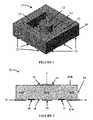
- FIG. 1is an isometric view of an example load sensor device.
- FIG. 2is a side view of the load sensor device of FIG. 1 .
- FIG. 3is a top view of the load sensor device of FIG. 1 .
- FIG. 4is a bottom view of the load sensor device of FIG. 1 .
- FIG. 5is a cross sectional view of the load sensor device of FIG. 1 along the line L of FIG. 3 .
- FIG. 6is a cross sectional view of the load sensor device along the line L of FIG. 3 , with a force F applied showing concentration of stresses within the device.
- FIG. 7is a cross sectional view of the load sensor device of FIG. 1 when electrically and mechanically connected to a circuit substrate and a touch surface.
- FIG. 8is an electrical schematic diagram of the electrical circuits embedded within the load sensor device of FIG. 1 .
- FIG. 9is an electrical schematic diagram of multiple load sensor devices of FIG. 1 in an independently addressable array.
- FIG. 10illustrates the process steps to manufacture the load sensor device of FIG. 1 .
- FIG. 11illustrates the process steps to electrically and mechanically attach the load sensor device of FIG. 1 to a separate circuit.
- the load sensor device 10includes a substrate 61 defining a deformable membrane 13 , a mesa 12 and an overload protection portion 15 .
- the overload protection portionas used herein can include a range of structures such as a ring, for example.
- the substrate 61can optionally be a silicon substrate. As shown in FIGS.
- the substrate 61can have a first surface 61 A and a second surface 61 B opposite the first surface 61 A, and the mesa 12 and the overload protection portion 15 can optionally be arranged in a central portion 61 C and a peripheral portion 61 D of the substrate 61 , respectively.
- the deformable membrane 13 , the mesa 12 and the overload protection portion 15can be formed from the substrate 61 using an etching process.
- at least one load sensor elemente.g., piezoresistive elements 14 and 82 discussed below
- the load sensor elementcan be a piezoresistive, piezoelectric or capacitive element.
- the load sensor elementcan be configured to change at least one electrical characteristic (e.g., resistance, charge, capacitance, etc.) based on an amount or magnitude of the applied force.
- the load sensor elementcan output a signal proportional to the amount or magnitude of the applied force.
- the mesa 12can define a contact surface 11 , for example along the top surface of the mesa 12 , for receiving an applied force F and transmitting the force F to the deformable membrane 13 .
- the contact surface 11can have any shape, such as, for example and without limitation, a substantially square shape, a substantially round, circular or elliptical shape as depicted in FIGS. 1-3 , a substantially rectangular shape, and the like. Additionally, this disclosure contemplates that the contact surface 11 can have shapes other than those described herein, and therefore, this disclosure should not be limited to the shapes described herein and/or shown in the figures. It is further contemplated, with reference to FIG.
- the contact surface 11can be affixed below a touch surface 71 in order to receive the reaction force F transmitted through the touch surface 71 as depicted in FIG. 7 .
- the contact surface 11can be bonded to at least a portion of the touch surface 71 using an adhesive.
- a strain gradientforms within the substrate 61 .
- the concentration of stresses in the load sensor device 10 in response to the applied force Fis illustrated in FIG. 6 .
- the strain gradientimparts a localized strain on the piezoresistive elements 14 and 82 (e.g., the load sensor elements).
- the piezoresistive elements 14 and 82experience strain, their respective resistivities change, such that a Wheatstone bridge circuit, e.g., the Wheatstone bridge circuit 81 of FIG. 8 , including two piezoresistive elements 14 and two oppositely arranged piezoresistive elements 82 (or stationary resistors) becomes unbalanced and produce a differential voltage across the positive signal terminal 83 and the negative signal terminal 84 .
- This differential voltageis directly proportional to the applied force F on the contact surface 11 .
- the load sensor device 10can include one or more electromechanical connectors 75 for electrically and mechanically connecting the load sensor device 10 to a separate circuit substrate.
- the load sensor device 10can include a touch surface (e.g., touch surface 71 ), for example, fixed to the contact surface 11 of the mesa 12 .
- the load sensor device 10incorporates an upper air gap 73 between the overload protection portion 15 and the touch surface 71 .
- the upper air gap 73exists because the height of the mesa 12 is greater than the height of the overload protection portion 15 .
- the difference in height between the mesa 12 and the overload protection portion 15can be selected or engineered to be less than the maximum vertical deflection of the deformable membrane 13 before it yields or fails due to an excessive applied force.
- the deformable membrane 13deforms, and when the force F reaches a threshold, the touch surface 71 comes into contact with the overload protection portion 15 . At this point, the deformable membrane 13 no longer deforms linearly with applied force F. In this way the upper air gap 73 and the overload protection portion 15 work together to prevent the load sensor device 10 (e.g., the deformable membrane 13 ) from mechanically failing under excessive applied force F.
- the load sensor device 10optionally incorporates a lower air gap 74 between a lower surface 16 of the load sensor device 10 and an upper surface of a separate circuit substrate 72 as shown in FIG. 7 .
- the deformable membrane 13deforms, allowing the touch surface 71 to move closer to and, as the force F becomes sufficiently large, come in contact with the overload protection portion 15 .
- the lower surface 16 of the load sensor device 10comes into contact with an upper surface 76 of the separate circuit substrate 72 .
- Electromechanical connectors 75such as a solder joints or wire bonds, can be provided. The electromechanical connectors 75 are used to electrically and mechanically connect the load sensor device 10 to the separate circuit substrate 72 .
- the load sensor device 10includes and/or incorporates electrical circuitry 80 to activate the load sensor device 10 and electrically connect the load sensor device 10 to a separate circuit signal bus, for example, through electromechanical connectors such as electromechanical connectors 75 of FIGS. 2 , 4 , 5 and 7 .
- the electromechanical connectorsare solder joints or wire bonds.
- the electrical circuitry 80can include the Wheatstone bridge circuit 81 .
- the electrical circuitry 80includes of an activation circuit 86 including an X row signal trace 90 and a Y column signal trace 91 and a logical gate (e.g., AND gate 89 ).
- the row and column signal traces 90 and 91can be used to individually address the load sensor device 10 .
- the AND gate 89is enabled, which closes a plurality of switches 87 .
- the electrical circuitry 80can also include one or more voltage supply traces for electrically connecting the Wheatstone bridge circuit 81 to an external voltage source 88 and one or more output signal traces for electrically connecting the positive and negative terminals 83 and 84 to the separate circuit signal bus.
- Each of the switchesrespectively, connects the external voltage source 88 to the Wheatstone bridge circuit 81 or connects the positive signal terminal 83 and the negative signal terminal 84 , respectively, to the separate circuit signal bus.
- an array of load sensor devices 10can be placed into an independently addressable array 90 , wherein the sensor value of each individual load sensor device 10 can be read independently, for example, by a microcontroller.
- An independently addressable array 90 including a plurality of load sensor device 10is depicted in FIG. 9 .
- step 110involves growing or depositing a layer of silicon oxide 151 onto a surface of a bare silicon wafer 150 .
- the layer of silicon oxideis grown or deposited on a surface of a silicon wafer on which electrical circuitry (e.g., the electrical circuitry 80 discussed above) for activating the load sensor device is already embedded through a separate CMOS semiconductor fabrication process.
- the silicon wafercan have an upper surface (or a first surface as used herein) and a lower surface (or a second surface as used herein) opposite to the upper surface.
- the surface of the silicon wafer on which the layer of silicon oxide is grown or deposited in step 110can be the upper surface of the silicon wafer.
- a layer of photoresist 152is applied or deposited onto at least a portion of the upper surface of the silicon wafer, for example, over the layer of silicon oxide. Thereafter, ultraviolet light is cast through a mask to weaken portions of the layer of photoresist. The layer of photoresist is then developed and at least a portion of the layer of silicon oxide 151 A is exposed, such that the exposed portion can be removed with an etchant as in step 112 .
- one or more piezoresistive elements 153are formed, for example, by a deposition, diffusion or ion implantation process.
- the piezoresistive elements 153can be the piezoresistive elements 14 and 82 discussed above, for example.
- step 114the layer of silicon oxide 151 is etched completely.
- step 115the silicon wafer is annealed and an additional layer of silicon oxide 154 is formed, for example, on the upper surface of the silicon wafer over the piezoresistive elements 153 . Additionally, a layer of silicon oxide 155 is also formed over on the opposite surface of the silicon wafer. It should be understood that the opposite surface of the silicon wafer as used herein can be the lower surface of the silicon wafer.
- step 116an additional layer of photoresist 156 is applied onto at least a portion of the upper surface of the silicon wafer, for example, over the layer of silicon oxide 154 .
- step 117the exposed portion of the layer of silicon oxide is etched completely to expose the piezoresistive elements 153 , e.g., an upper portion of the piezoresistive elements 153 .
- a conductive metal 157(e.g., an electrical trace), such as aluminum, is sputtered onto the upper surface of the silicon wafer, for example, over the exposed piezoresistive elements, to form electrical connections between the piezoresistive elements 153 and the electromechanical connectors (discussed below).
- an additional layer of photoresist 158is applied onto at least a portion of the upper surface of the silicon wafer, for example, over the conductive metal. Thereafter, ultraviolet light is cast through a mask, which weakens at least a portion of the layer of photoresist. The layer of photoresist is then developed in order to expose at least a portion of the conductive metal 157 A to be removed.
- the exposed portion of the conductive metalis etched completely to leave the remaining conductive metal forming one or more portions of the connecting circuitry (e.g., one or more portions of the electrical circuitry 80 discussed above).
- a passivation layer 159is deposited or applied to protect the piezoresistive elements 153 and conductive metal 157 .
- an additional layer of photoresist 160is applied to the upper surface of the silicon wafer, for example, over the passivation layer. Thereafter, ultraviolet light is cast through a mask to weaken at least a portion of the layer of photoresist. The layer of photoresist is then developed in order to expose at least a portion of the passivation layer 159 A to be removed.
- the exposed portion of the passivation layeris etched completely to leave a portion of the conductive metal 157 B underneath exposed for electrical contact.
- step 124the silicon wafer is inverted to expose the lower surface of the silicon wafer.
- the lower surface of the silicon waferhas the layer of silicon oxide 155 formed thereon.
- an additional layer of photoresist 161is applied to the lower surface of the silicon wafer, for example, over a portion of the layer of silicon oxide. Thereafter, ultraviolet light is cast through a mask to weaken at least a portion of the layer of photoresist. The layer of photoresist is then developed in order to expose at least a portion of the layer of silicon oxide 155 A formed over the lower surface of the silicon wafer.
- step 125the exposed portion of the layer of silicon oxide is etched completely to expose a portion of the lower surface of the silicon wafer 150 A.
- step 126the exposed portion of silicon wafer is etched to form the height offset between a mesa and overload protection portion (e.g., the mesa 12 and overload protection portion 15 discussed above) to provide overload protection.
- step 127an additional layer of photoresist 162 is applied onto at least a portion of the lower surface of the silicon wafer. Thereafter, ultraviolet light is cast through a mask to weaken at least a portion of the layer of photoresist. The layer of photoresist is then developed in order to expose at least a portion of the lower surface of the silicon wafer 150 B.
- step 128the silicon on the lower surface of the silicon wafer is etched away using a deep reactive ion etching process to form an integrated mesa, contact surface, deformable membrane and overload protection portion (e.g., the mesa 12 , contact surface 11 , deformable membrane 13 and overload protection portion 15 ).
- step 129the layer of silicon oxide on the upper surface of the mesa is etched completely to leave exposed bare silicon.
- the silicon wafercan then optionally be inverted and electromechanical connectors (e.g., electromechanical connectors 75 discussed above) such as solder bumps, wire bonds, etc. are attached to the load sensor device, e.g., to the same surface of the bare silicon wafer on which the piezoresistive elements were formed.
- the load sensor deviceis then ready for a separate manufacturing process to be attached to an electrical circuit.
- a load sensor devicee.g., load sensor device 10 of FIGS. 1-7
- a separate circuit substratee.g., separate circuit substrate 72 of FIG. 7
- the load sensor devicesare first bonded to the substrate, such as FR 4 , of a separate circuit.
- the electrical and mechanical connectionsare formed through a process such as reflow soldering or wire bonding.
- a touch surfacee.g., touch surface 71 of FIG. 7
- each load sensor devicee.g., to the contact surface 11 of the mesa 12 of each load sensor 10 of FIGS. 1-7
- adhesivee.g., to the entire assembly is cured to form a finished touch surface component.
Landscapes
- Engineering & Computer Science (AREA)
- Physics & Mathematics (AREA)
- General Physics & Mathematics (AREA)
- Manufacturing & Machinery (AREA)
- Microelectronics & Electronic Packaging (AREA)
- Power Engineering (AREA)
- Chemical & Material Sciences (AREA)
- Analytical Chemistry (AREA)
- Computer Hardware Design (AREA)
- Pressure Sensors (AREA)
Abstract
Description
This application claims the benefit of U.S. Provisional Patent Application No. 61/668,135, filed on Jul. 5, 2012, entitled “Microelectromechanical Load Sensor and Methods of Using Same,” the disclosure of which is expressly incorporated herein by reference in its entirety.
This disclosure relates to the technical field of touch interfaces based on microelectromechanical (“MEMS”) load sensors that are used as input devices for data processing systems.
A variety of known MEMS devices are designed to measure applied load and produce an output differential voltage signal proportional to the applied load. These known devices, such as conventional piezoresistive, piezoelectric, and capacitive MEMS force sensors, pressure sensors, and strain gauges, utilize the unique electromechanical properties of materials such as silicon and lead zirconate titanate.
However, there is a need in the pertinent art for an interface device that is capable of receiving and recognizing a range of human user actions. There is also a need in the pertinent art for an interface device that is capable of tolerating a force from a user without being damaged or causing injury to the user.
Described herein are MEMS load sensor devices and, more specifically, MEMS load sensor devices designed to measure an applied load and produce an output signal. More specifically, the MEMS load sensor devices described herein are configured to measure forces originating from human user actions such as pressing a button or a touch surface. The MEMS load sensor devices can be configured as a component of a force sensitive touch interface for providing touch input into a data processing system, for example. The MEMS load sensor devices can include a substrate, a deformable membrane, a load sensor element configured to produce a signal when deformed, an overload protection portion, and a means to communicate load sensor signals to an electrical circuit.
An example MEMS load sensor device can include a substrate defining a deformable membrane, a mesa and an overload protection portion. The mesa can be configured to receive and transfer an applied force to the deformable membrane, and the deformable membrane can be configured to deform in response to the applied force. The MEMS load sensor device can also include at least one load sensor element formed on the deformable membrane. The load sensor element can be configured to change at least one electrical characteristic based on an amount or magnitude of the applied force. Additionally, a height of the mesa can be greater than a height of the overload protection portion.
Optionally, the mesa defines a contact surface for receiving the applied force. The contact surface can have at least one of a substantially square, rectangular, rounded, circular or elliptical shape.
Alternatively or additionally, the mesa can optionally be arranged in a central portion of the substrate. Alternatively or additionally, the overload protection portion can optionally be arranged in a peripheral portion of the substrate.
Optionally, the MEMS load sensor device can further include a touch surface fixed to at least a portion of the mesa. The touch surface can be configured to receive and transfer the applied force to the mesa. Additionally, a gap can be arranged between the touch surface and the overload protection portion when the touch surface is fixed to the mesa. The gap can limit an amount of deflection of the deformable membrane and can prevent the deformable membrane from mechanically failing under an excessive applied force.
Alternatively or additionally, the MEMS load sensor device can optionally include one or more electromechanical connectors for connecting the MEMS load sensor device to an external circuit.
Optionally, the deformable membrane, the mesa and the overload protection portion can be formed by removing a portion of the substrate. For example, the substrate can have a first surface and a second surface opposite to the first surface. The deformable membrane, the mesa and the overload protection portion can be formed using a deep reactive ion etching technique on the second surface. Additionally, the MEMS load sensor device can optionally include one or more electromechanical connectors for connecting the MEMS load sensor device to an external circuit formed on the first surface.
Optionally, the load sensor element can be a piezoresistive element. Additionally, the MEMS load sensor device can include a plurality of piezoresistive elements electrically connected in a Wheatstone bridge circuit. Additionally, the MEMS load sensor device can optionally include an activation circuit for supplying a voltage to the Wheatstone bridge circuit and for communicating a differential output voltage from the Wheatstone bridge circuit. For example, the activation circuit can include one or more output signal traces for communicating the differential output voltage from the Wheatstone bridge circuit to a signal bus and one or more voltage supply traces for connecting the Wheatstone bridge circuit to an external voltage source. The MEMS load sensor device can also include a row trace and a column trace for addressing the MEMS load sensor device and a logical gate having an input and output and one or more switches connected to the output of the logical gate. The input of the logical gate can be connected to the row and column traces, and each switch can be configured to electrically connect an output trace and the signal bus or a voltage supply trace and the external voltage source.
Also described herein is a method of manufacturing a MEMS load sensor device and optionally electrically and mechanically attaching the MEMS load sensor device to a separate circuit substrate. For example, the method includes the steps to manufacture the MEMS load sensor device and also optionally includes the steps to attach the MEMS load sensor device to the separate circuit substrate. The steps include micromachining the mechanical elements such as the deformable membrane, mesa, and overload protection portion, forming (e.g., by ion implantation) a load sensor element such as a piezoresistive element, metallization steps to form traces to connect the piezoresistive element to other electrical circuit elements on the MEMS load sensor device, steps to embed complementary metal-oxide-semiconductor (“CMOS”) circuitry to activate the MEMS load sensor device and to connect the MEMS load sensor device output to a signal bus of a separate circuit, steps to add electrical and mechanical connectors, and post processing steps to electrically and mechanically attach the MEMS load sensor device to a separate circuit substrate.
An example method for manufacturing a MEMS load sensor device can include providing a substrate having a first surface and a second surface opposite to the first surface, forming at least one load sensor element on the first surface of the substrate and etching the second surface of the substrate to form a deformable membrane, a mesa and an overload protection portion. The mesa can be configured to receive and transfer an applied force to the deformable membrane, and the deformable membrane can be configured to deform in response to the applied force. Additionally, the load sensor element can be provided on the deformable membrane and can be configured to change at least one electrical characteristic based on an amount or magnitude of the applied force. A height of the mesa can be greater than a height of the overload protection portion.
Optionally, in the method above, etching the second surface of the substrate to form a deformable membrane, a mesa and an overload protection portion can further include applying a layer of photoresist over the second surface of the substrate, irradiating a portion of the layer of photoresist with ultraviolet light through a mask and removing the irradiated portion of the layer of photoresist to expose a portion of the second surface of the substrate. Thereafter, the method can further include etching the exposed portion of the second surface of the substrate to form the deformable membrane, the mesa and the overload protection portion. For example, the second surface of the substrate can be etched using a deep ion etching technique.
Alternatively or additionally, in the method above, forming at least one load sensor element on the first surface of the substrate can further include applying a layer of silicon oxide over the first surface of the substrate, applying a layer of photoresist over the layer of silicon oxide, irradiating a portion of the layer of photoresist with ultraviolet light through a mask and removing the irradiated portion of the layer of photoresist to expose a portion of the layer of silicon oxide. Thereafter, the method can further include etching the exposed portion of the layer of silicon oxide to expose a portion of the first layer of the substrate and forming the load sensor element on the exposed portion of the first layer of the substrate.
Optionally, the load sensor element can be a piezoresistive element formed using a deposition, diffusion, or ion implantation technique.
Alternatively or additionally, the method can optionally include forming at least one electrical trace on the first surface of the substrate. The electrical trace can be electrically connected to the load sensor element.
Alternatively or additionally, the method can optionally further include forming one or more electromechanical connectors for connecting the MEMS load sensor device to an external circuit.
Optionally, the mesa defines a contact surface for receiving the applied force. The contact surface can have at least one of a substantially square, rectangular, rounded, circular or elliptical shape.
Alternatively or additionally, the mesa can optionally be arranged in a central portion of the substrate. Alternatively or additionally, the overload protection portion can optionally be arranged in a peripheral portion of the substrate.
Optionally, the method can further include fixing a touch surface to at least a portion of the mesa. The touch surface can be configured to receive and transfer the applied force to the mesa. Additionally, a gap can be arranged between the touch surface and the overload protection portion when the touch surface is fixed to the mesa. The gap can limit an amount of deflection of the deformable membrane and can prevent the deformable membrane from mechanically failing under an excessive applied force.
Other systems, methods, features and/or advantages will be or may become apparent to one with skill in the art upon examination of the following drawings and detailed description. It is intended that all such additional systems, methods, features and/or advantages be included within this description and be protected by the accompanying claims.
The components in the drawings are not necessarily to scale relative to each other. Like reference numerals designate corresponding parts throughout the several views.
Unless defined otherwise, all technical and scientific terms used herein have the same meaning as commonly understood by one of ordinary skill in the art. Methods and materials similar or equivalent to those described herein can be used in the practice or testing of the present disclosure. As used in the specification, and in the appended claims, the singular forms “a,” “an,” “the” include plural referents unless the context clearly dictates otherwise. The term “comprising” and variations thereof as used herein is used synonymously with the term “including” and variations thereof and are open, non-limiting terms. The terms “optional” or “optionally” used herein mean that the subsequently described feature, event or circumstance may or may not occur, and that the description includes instances where said feature, event or circumstance occurs and instances where it does not. While implementations will be described with respect to a MEMS load sensor device and method of manufacturing the same, it will become evident to those skilled in the art that the implementations are not limited thereto.
Described herein is an example MEMS load sensor device (e.g., load sensor device) for measuring a force applied to a least a portion thereof. In one aspect, as depicted inFIGS. 1-6 , theload sensor device 10 includes asubstrate 61 defining adeformable membrane 13, amesa 12 and anoverload protection portion 15. It should be understood that the overload protection portion as used herein can include a range of structures such as a ring, for example. Thesubstrate 61 can optionally be a silicon substrate. As shown inFIGS. 1 and 2 , thesubstrate 61 can have afirst surface 61A and asecond surface 61B opposite thefirst surface 61A, and themesa 12 and theoverload protection portion 15 can optionally be arranged in acentral portion 61C and aperipheral portion 61D of thesubstrate 61, respectively. As discussed in more detail below, thedeformable membrane 13, themesa 12 and theoverload protection portion 15 can be formed from thesubstrate 61 using an etching process. Additionally, at least one load sensor element (e.g.,piezoresistive elements deformable membrane 13. Optionally the load sensor element can be a piezoresistive, piezoelectric or capacitive element. The load sensor element can be configured to change at least one electrical characteristic (e.g., resistance, charge, capacitance, etc.) based on an amount or magnitude of the applied force. Optionally, the load sensor element can output a signal proportional to the amount or magnitude of the applied force.
Additionally, themesa 12 can define acontact surface 11, for example along the top surface of themesa 12, for receiving an applied force F and transmitting the force F to thedeformable membrane 13. It is contemplated that thecontact surface 11 can have any shape, such as, for example and without limitation, a substantially square shape, a substantially round, circular or elliptical shape as depicted inFIGS. 1-3 , a substantially rectangular shape, and the like. Additionally, this disclosure contemplates that thecontact surface 11 can have shapes other than those described herein, and therefore, this disclosure should not be limited to the shapes described herein and/or shown in the figures. It is further contemplated, with reference toFIG. 3 , that thecontact surface 11 can be affixed below atouch surface 71 in order to receive the reaction force F transmitted through thetouch surface 71 as depicted inFIG. 7 . For example, as discussed below, at least a portion of thecontact surface 11 can be bonded to at least a portion of thetouch surface 71 using an adhesive. As thedeformable membrane 13 deforms, a strain gradient forms within thesubstrate 61. The concentration of stresses in theload sensor device 10 in response to the applied force F is illustrated inFIG. 6 . The strain gradient imparts a localized strain on thepiezoresistive elements 14 and82 (e.g., the load sensor elements). As thepiezoresistive elements Wheatstone bridge circuit 81 ofFIG. 8 , including twopiezoresistive elements 14 and two oppositely arranged piezoresistive elements82 (or stationary resistors) becomes unbalanced and produce a differential voltage across thepositive signal terminal 83 and thenegative signal terminal 84. This differential voltage is directly proportional to the applied force F on thecontact surface 11. In addition, theload sensor device 10 can include one or moreelectromechanical connectors 75 for electrically and mechanically connecting theload sensor device 10 to a separate circuit substrate.
As discussed above, theload sensor device 10 can include a touch surface (e.g., touch surface71), for example, fixed to thecontact surface 11 of themesa 12. In an additional aspect, theload sensor device 10 incorporates anupper air gap 73 between theoverload protection portion 15 and thetouch surface 71. As shown inFIG. 7 , theupper air gap 73 exists because the height of themesa 12 is greater than the height of theoverload protection portion 15. The difference in height between themesa 12 and theoverload protection portion 15 can be selected or engineered to be less than the maximum vertical deflection of thedeformable membrane 13 before it yields or fails due to an excessive applied force. As the force F is applied to thetouch surface 71, thedeformable membrane 13 deforms, and when the force F reaches a threshold, thetouch surface 71 comes into contact with theoverload protection portion 15. At this point, thedeformable membrane 13 no longer deforms linearly with applied force F. In this way theupper air gap 73 and theoverload protection portion 15 work together to prevent the load sensor device10 (e.g., the deformable membrane13) from mechanically failing under excessive applied force F.
Alternatively or additionally, theload sensor device 10 optionally incorporates alower air gap 74 between alower surface 16 of theload sensor device 10 and an upper surface of aseparate circuit substrate 72 as shown inFIG. 7 . As the force F is applied to thetouch surface 71, thedeformable membrane 13 deforms, allowing thetouch surface 71 to move closer to and, as the force F becomes sufficiently large, come in contact with theoverload protection portion 15. Alternatively or additionally, as the force F becomes sufficiently larger and thedeformable membrane 13 deforms lower, thelower surface 16 of theload sensor device 10 comes into contact with anupper surface 76 of theseparate circuit substrate 72. Once force F reaches an upper threshold and thetouch surface 71 is in contact with theoverload protection portion 15 and thelower surface 16 of theload sensor device 10 comes into contact with theupper surface 76 of theseparate circuit substrate 72, thedeformable membrane 13 no longer deforms linearly with applied force F. In this way theupper air gap 73, thelower air gap 74, and theoverload protection portion 15 work together to prevent the load sensor device10 (e.g., the deformable membrane13) from mechanically failing under excessive applied force F.Electromechanical connectors 75, such as a solder joints or wire bonds, can be provided. Theelectromechanical connectors 75 are used to electrically and mechanically connect theload sensor device 10 to theseparate circuit substrate 72.
Referring now toFIG. 8 , in an additional aspect, theload sensor device 10 includes and/or incorporateselectrical circuitry 80 to activate theload sensor device 10 and electrically connect theload sensor device 10 to a separate circuit signal bus, for example, through electromechanical connectors such aselectromechanical connectors 75 ofFIGS. 2 ,4,5 and7. Optionally, the electromechanical connectors are solder joints or wire bonds. As discussed above, theelectrical circuitry 80 can include theWheatstone bridge circuit 81. In one embodiment, theelectrical circuitry 80 includes of anactivation circuit 86 including an Xrow signal trace 90 and a Ycolumn signal trace 91 and a logical gate (e.g., AND gate89). The row and column signal traces90 and91 can be used to individually address theload sensor device 10. For example, when both X and Y signals are logic high, the ANDgate 89 is enabled, which closes a plurality ofswitches 87. Theelectrical circuitry 80 can also include one or more voltage supply traces for electrically connecting theWheatstone bridge circuit 81 to anexternal voltage source 88 and one or more output signal traces for electrically connecting the positive andnegative terminals external voltage source 88 to theWheatstone bridge circuit 81 or connects thepositive signal terminal 83 and thenegative signal terminal 84, respectively, to the separate circuit signal bus. In this way, an array ofload sensor devices 10 can be placed into an independentlyaddressable array 90, wherein the sensor value of each individualload sensor device 10 can be read independently, for example, by a microcontroller. An independentlyaddressable array 90 including a plurality ofload sensor device 10 is depicted inFIG. 9 .
Referring now toFIG. 10 , a method for manufacturing a MEMS load sensor device such as theload sensor device 10 discussed above is described herein. In the described method,step 110 involves growing or depositing a layer ofsilicon oxide 151 onto a surface of abare silicon wafer 150. Optionally, the layer of silicon oxide is grown or deposited on a surface of a silicon wafer on which electrical circuitry (e.g., theelectrical circuitry 80 discussed above) for activating the load sensor device is already embedded through a separate CMOS semiconductor fabrication process. It should be understood that the silicon wafer can have an upper surface (or a first surface as used herein) and a lower surface (or a second surface as used herein) opposite to the upper surface. The surface of the silicon wafer on which the layer of silicon oxide is grown or deposited instep 110 can be the upper surface of the silicon wafer. Instep 111, a layer ofphotoresist 152 is applied or deposited onto at least a portion of the upper surface of the silicon wafer, for example, over the layer of silicon oxide. Thereafter, ultraviolet light is cast through a mask to weaken portions of the layer of photoresist. The layer of photoresist is then developed and at least a portion of the layer ofsilicon oxide 151A is exposed, such that the exposed portion can be removed with an etchant as instep 112. In step113, one or more piezoresistive elements153 (e.g., load sensors elements) are formed, for example, by a deposition, diffusion or ion implantation process. Thepiezoresistive elements 153 can be thepiezoresistive elements
Instep 114, the layer ofsilicon oxide 151 is etched completely. Instep 115, the silicon wafer is annealed and an additional layer ofsilicon oxide 154 is formed, for example, on the upper surface of the silicon wafer over thepiezoresistive elements 153. Additionally, a layer ofsilicon oxide 155 is also formed over on the opposite surface of the silicon wafer. It should be understood that the opposite surface of the silicon wafer as used herein can be the lower surface of the silicon wafer. Instep 116, an additional layer ofphotoresist 156 is applied onto at least a portion of the upper surface of the silicon wafer, for example, over the layer ofsilicon oxide 154. Thereafter, ultraviolet light is cast through a mask, which weakens portions of the layer ofphotoresist 156. The layer of photoresist is then developed in order to expose at least a portion of the layer ofsilicon oxide 154A covering thepiezoresistive elements 153. Instep 117, the exposed portion of the layer of silicon oxide is etched completely to expose thepiezoresistive elements 153, e.g., an upper portion of thepiezoresistive elements 153. Instep 118, a conductive metal157 (e.g., an electrical trace), such as aluminum, is sputtered onto the upper surface of the silicon wafer, for example, over the exposed piezoresistive elements, to form electrical connections between thepiezoresistive elements 153 and the electromechanical connectors (discussed below). Instep 119, an additional layer ofphotoresist 158 is applied onto at least a portion of the upper surface of the silicon wafer, for example, over the conductive metal. Thereafter, ultraviolet light is cast through a mask, which weakens at least a portion of the layer of photoresist. The layer of photoresist is then developed in order to expose at least a portion of theconductive metal 157A to be removed. Instep 120, the exposed portion of the conductive metal is etched completely to leave the remaining conductive metal forming one or more portions of the connecting circuitry (e.g., one or more portions of theelectrical circuitry 80 discussed above).
Instep 121, apassivation layer 159 is deposited or applied to protect thepiezoresistive elements 153 andconductive metal 157. Instep 122, an additional layer ofphotoresist 160 is applied to the upper surface of the silicon wafer, for example, over the passivation layer. Thereafter, ultraviolet light is cast through a mask to weaken at least a portion of the layer of photoresist. The layer of photoresist is then developed in order to expose at least a portion of thepassivation layer 159A to be removed. Instep 123, the exposed portion of the passivation layer is etched completely to leave a portion of theconductive metal 157B underneath exposed for electrical contact.
Instep 124, the silicon wafer is inverted to expose the lower surface of the silicon wafer. As discussed above with regard to step115, the lower surface of the silicon wafer has the layer ofsilicon oxide 155 formed thereon. In addition, an additional layer ofphotoresist 161 is applied to the lower surface of the silicon wafer, for example, over a portion of the layer of silicon oxide. Thereafter, ultraviolet light is cast through a mask to weaken at least a portion of the layer of photoresist. The layer of photoresist is then developed in order to expose at least a portion of the layer ofsilicon oxide 155A formed over the lower surface of the silicon wafer. Instep 125, the exposed portion of the layer of silicon oxide is etched completely to expose a portion of the lower surface of thesilicon wafer 150A. Instep 126, the exposed portion of silicon wafer is etched to form the height offset between a mesa and overload protection portion (e.g., themesa 12 andoverload protection portion 15 discussed above) to provide overload protection. Instep 127, an additional layer ofphotoresist 162 is applied onto at least a portion of the lower surface of the silicon wafer. Thereafter, ultraviolet light is cast through a mask to weaken at least a portion of the layer of photoresist. The layer of photoresist is then developed in order to expose at least a portion of the lower surface of thesilicon wafer 150B. Instep 128, the silicon on the lower surface of the silicon wafer is etched away using a deep reactive ion etching process to form an integrated mesa, contact surface, deformable membrane and overload protection portion (e.g., themesa 12,contact surface 11,deformable membrane 13 and overload protection portion15). Instep 129, the layer of silicon oxide on the upper surface of the mesa is etched completely to leave exposed bare silicon. The silicon wafer can then optionally be inverted and electromechanical connectors (e.g.,electromechanical connectors 75 discussed above) such as solder bumps, wire bonds, etc. are attached to the load sensor device, e.g., to the same surface of the bare silicon wafer on which the piezoresistive elements were formed. The load sensor device is then ready for a separate manufacturing process to be attached to an electrical circuit.
Referring now toFIG. 11 , the steps to attach a load sensor device (e.g.,load sensor device 10 ofFIGS. 1-7 ) to a separate circuit substrate (e.g.,separate circuit substrate 72 ofFIG. 7 ) and complete a touch solution are illustrated. In this final manufacturing process, the load sensor devices are first bonded to the substrate, such as FR4, of a separate circuit. Then, the electrical and mechanical connections are formed through a process such as reflow soldering or wire bonding. Finally, a touch surface (e.g.,touch surface 71 ofFIG. 7 ) is affixed to each load sensor device (e.g., to thecontact surface 11 of themesa 12 of eachload sensor 10 ofFIGS. 1-7 ) in the finished component using adhesive, and the entire assembly is cured to form a finished touch surface component.
Although the subject matter has been described in language specific to structural features and/or methodological acts, it is to be understood that the subject matter defined in the appended claims is not necessarily limited to the specific features or acts described above. Rather, the specific features and acts described above are disclosed as example forms of implementing the claims.
Claims (20)
1. A microelectromechanical (MEMS) load sensor device, comprising:
a substrate defining a deformable membrane, a mesa and an overload protection portion, the mesa being configured to receive and transfer an applied force to the deformable membrane, the deformable membrane being configured to deform in response to the applied force; and
at least one load sensor element formed on the deformable membrane, the load sensor element being configured to change at least one electrical characteristic based on an amount or magnitude of the applied force, wherein a height of the mesa is greater than a height of the overload protection portion.
2. The MEMS load sensor device ofclaim 1 , wherein the mesa defines a contact surface for receiving the applied force.
3. The MEMS load sensor device of2, wherein the contact surface has at least one of a substantially square, rectangular, rounded, circular or elliptical shape.
4. The MEMS load sensor device of any ofclaim 1 , wherein the mesa is arranged in a central portion of the substrate.
5. The MEMS load sensor device ofclaim 1 , wherein the overload protection portion is arranged in a peripheral portion of the substrate.
6. The MEMS load sensor device ofclaim 1 , further comprising a touch surface fixed to at least a portion of the mesa, wherein the touch surface is configured to receive and transfer the applied force to the mesa.
7. The MEMS load sensor device ofclaim 6 , wherein a gap is arranged between the touch surface and the overload protection portion when the touch surface is fixed to the mesa, the gap limiting an amount of deflection of the deformable membrane and preventing the deformable membrane from mechanically failing under an excessive applied force.
8. The MEMS load sensor device ofclaim 1 , further comprising one or more electromechanical connectors for connecting the MEMS load sensor device to an external circuit.
9. The MEMS load sensor device ofclaim 1 , wherein the deformable membrane, the mesa and the overload protection portion are formed by removing a portion of the substrate.
10. The MEMS load sensor device ofclaim 9 , wherein the substrate has a first surface and a second surface opposite to the first surface, and the deformable membrane, the mesa and the overload protection portion are formed using a deep reactive ion etching technique on the second surface.
11. The MEMS load sensor device ofclaim 10 , wherein one or more electromechanical connectors for connecting the MEMS load sensor device to an external circuit are formed on the first surface.
12. The MEMS load sensor device ofclaim 1 , wherein the load sensor element comprises a piezoresistive element.
13. The MEMS load sensor device ofclaim 12 , further comprising a plurality of piezoresistive elements electrically connected in a Wheatstone bridge circuit.
14. The MEMS load sensor device ofclaim 13 , further comprising an activation circuit for supplying a voltage to the Wheatstone bridge circuit and for communicating a differential output voltage from the Wheatstone bridge circuit.
15. The MEMS load sensor device ofclaim 14 , wherein the activation circuit comprises:
one or more output signal traces for communicating the differential output voltage from the Wheatstone bridge circuit to a signal bus;
one or more voltage supply traces for connecting the Wheatstone bridge circuit to an external voltage source;
a row trace and a column trace for addressing the MEMS load sensor device;
a logical gate having an input and output, the input of the logical gate being connected to the row and column traces; and
one or more switches connected to the output of the logical gate, wherein each switch is configured to electrically connect an output trace and the signal bus or a voltage supply trace and the external voltage source.
16. A method for manufacturing a microelectromechanical (MEMS) load sensor device, comprising:
providing a substrate having a first surface and a second surface opposite to the first surface;
forming at least one load sensor element on the first surface of the substrate; and
etching the second surface of the substrate to form a deformable membrane, a mesa and an overload protection portion, the mesa being configured to receive and transfer an applied force to the deformable membrane, the deformable membrane being configured to deform in response to the applied force, and the load sensor element being provided on the deformable membrane and being configured to change at least one electrical characteristic based on an amount or magnitude of the applied force, wherein a height of the mesa is greater than a height of the overload protection portion.
17. The method ofclaim 16 , wherein etching the second surface of the substrate to form a deformable membrane, a mesa and an overload protection portion further comprises:
applying a layer of photoresist over the second surface of the substrate;
irradiating a portion of the layer of photoresist with ultraviolet light through a mask;
removing the irradiated portion of the layer of photoresist to expose a portion of the second surface of the substrate; and
etching the exposed portion of the second surface of the substrate to form the deformable membrane, the mesa and the overload protection portion.
18. The method ofclaim 16 , wherein forming at least one load sensor element on the first surface of the substrate further comprises:
applying a layer of silicon oxide over the first surface of the substrate;
applying a layer of photoresist over the layer of silicon oxide;
irradiating a portion of the layer of photoresist with ultraviolet light through a mask;
removing the irradiated portion of the layer of photoresist to expose a portion of the layer of silicon oxide;
etching the exposed portion of the layer of silicon oxide to expose a portion of the first layer of the substrate; and
forming the load sensor element on the exposed portion of the first layer of the substrate.
19. The method ofclaim 18 , wherein the load sensor element is a piezoresistive element formed using an ion implantation technique.
20. The method ofclaim 16 , further comprising fixing a touch surface to at least a portion of the mesa, wherein the touch surface is configured to receive and transfer the applied force to the mesa, wherein a gap is arranged between the touch surface and the overload protection portion when the touch surface is fixed to the mesa, the gap limiting an amount of deflection of the deformable membrane and preventing the deformable membrane from mechanically failing under an excessive applied force.
Priority Applications (1)
| Application Number | Priority Date | Filing Date | Title |
|---|---|---|---|
| US13/934,900US9032818B2 (en) | 2012-07-05 | 2013-07-03 | Microelectromechanical load sensor and methods of manufacturing the same |
Applications Claiming Priority (2)
| Application Number | Priority Date | Filing Date | Title |
|---|---|---|---|
| US201261668135P | 2012-07-05 | 2012-07-05 | |
| US13/934,900US9032818B2 (en) | 2012-07-05 | 2013-07-03 | Microelectromechanical load sensor and methods of manufacturing the same |
Publications (2)
| Publication Number | Publication Date |
|---|---|
| US20140007705A1 US20140007705A1 (en) | 2014-01-09 |
| US9032818B2true US9032818B2 (en) | 2015-05-19 |
Family
ID=48803618
Family Applications (1)
| Application Number | Title | Priority Date | Filing Date |
|---|---|---|---|
| US13/934,900ActiveUS9032818B2 (en) | 2012-07-05 | 2013-07-03 | Microelectromechanical load sensor and methods of manufacturing the same |
Country Status (3)
| Country | Link |
|---|---|
| US (1) | US9032818B2 (en) |
| EP (1) | EP2870445A1 (en) |
| WO (1) | WO2014008377A1 (en) |
Cited By (23)
| Publication number | Priority date | Publication date | Assignee | Title |
|---|---|---|---|---|
| US20150090042A1 (en)* | 2013-09-27 | 2015-04-02 | Infineon Technologies Ag | Pressure Sensor Package with Integrated Sealing |
| US20170102274A1 (en)* | 2014-03-26 | 2017-04-13 | Denso Corporation | Force detection apparatus |
| CN107121223A (en)* | 2016-02-24 | 2017-09-01 | 英属开曼群岛商智动全球股份有限公司 | Microcomputer power quantity sensor and force sensing apparatus |
| WO2017184809A1 (en) | 2016-04-20 | 2017-10-26 | Nextinput, Inc. | Force-sensitive electronic device |
| US20180179050A1 (en)* | 2014-01-13 | 2018-06-28 | Nextinput, Inc. | Miniaturized and ruggedized wafer level mems force sensors |
| US10260981B2 (en)* | 2017-02-06 | 2019-04-16 | Nxp Usa, Inc. | Pressure sensor having sense elements in multiple wheatstone bridges with chained outputs |
| US10373790B2 (en)* | 2014-02-14 | 2019-08-06 | Fraunhofe-Gesellschaft Zur Foerderung Der Angewandten Forschung E.V. | Micro-electro-mechanical system and method for producing the same |
| US10571348B2 (en) | 2016-08-30 | 2020-02-25 | Honeywell International Inc. | Overforce control through sense die design |
| US10831292B2 (en) | 2014-08-04 | 2020-11-10 | Nextinput, Inc. | Force sensitive touch panel devices |
| US11221263B2 (en) | 2017-07-19 | 2022-01-11 | Nextinput, Inc. | Microelectromechanical force sensor having a strain transfer layer arranged on the sensor die |
| US11243126B2 (en)* | 2017-07-27 | 2022-02-08 | Nextinput, Inc. | Wafer bonded piezoresistive and piezoelectric force sensor and related methods of manufacture |
| US11255737B2 (en)* | 2017-02-09 | 2022-02-22 | Nextinput, Inc. | Integrated digital force sensors and related methods of manufacture |
| US11423686B2 (en) | 2017-07-25 | 2022-08-23 | Qorvo Us, Inc. | Integrated fingerprint and force sensor |
| US11579028B2 (en) | 2017-10-17 | 2023-02-14 | Nextinput, Inc. | Temperature coefficient of offset compensation for force sensor and strain gauge |
| US11604104B2 (en) | 2017-02-09 | 2023-03-14 | Qorvo Us, Inc. | Integrated piezoresistive and piezoelectric fusion force sensor |
| US20230236075A1 (en)* | 2022-01-26 | 2023-07-27 | Alps Alpine Co., Ltd. | Load sensor device |
| US11712501B2 (en) | 2019-11-12 | 2023-08-01 | Fresenius Medical Care Deutschland Gmbh | Blood treatment systems |
| US11730871B2 (en) | 2019-11-12 | 2023-08-22 | Fresenius Medical Care Deutschland Gmbh | Blood treatment systems |
| US11752247B2 (en) | 2019-11-12 | 2023-09-12 | Fresenius Medical Care Deutschland Gmbh | Blood treatment systems |
| US11874185B2 (en)* | 2017-11-16 | 2024-01-16 | Nextinput, Inc. | Force attenuator for force sensor |
| US11925736B2 (en) | 2019-11-12 | 2024-03-12 | Fresenius Medical Care Deutschland Gmbh | Blood treatment systems |
| US12285553B2 (en) | 2019-11-12 | 2025-04-29 | Fresenius Medical Care Deutschland Gmbh | Blood treatment systems |
| US12329890B2 (en) | 2019-11-12 | 2025-06-17 | Fresenius Medical Care Deutschland Gmbh | Blood treatment systems |
Families Citing this family (21)
| Publication number | Priority date | Publication date | Assignee | Title |
|---|---|---|---|---|
| WO2012106799A1 (en)* | 2011-02-07 | 2012-08-16 | The Governors Of The University Of Alberta | Piezoresistive load sensor |
| US9493342B2 (en) | 2012-06-21 | 2016-11-15 | Nextinput, Inc. | Wafer level MEMS force dies |
| US10190927B2 (en)* | 2014-03-03 | 2019-01-29 | National University Corporation Kagawa University | Tactile sensor and method for evaluating touch feeling |
| CN104215362A (en)* | 2014-06-24 | 2014-12-17 | 无锡壹资半导体科技有限公司 | Piezoresistive high-overload pressure sensor and manufacture method thereof |
| CN104236764B (en)* | 2014-09-29 | 2016-05-11 | 合肥工业大学 | A kind of capacitive touch sliding feeling sensor device |
| PL3018451T3 (en) | 2014-11-05 | 2017-12-29 | Nokia Technologies Oy | An apparatus and method for sensing |
| EP3230706B1 (en) | 2014-12-09 | 2021-02-03 | Technion Research & Development Foundation Ltd. | High resolution pressure sensing |
| JP2016217804A (en)* | 2015-05-18 | 2016-12-22 | タッチエンス株式会社 | Multi-axis tactile sensor and method for manufacturing multi-axis tactile sensor |
| CN107848788B (en) | 2015-06-10 | 2023-11-24 | 触控解决方案股份有限公司 | Ruggedized wafer-level MEMS force sensor with tolerance trench |
| AU2017280145B2 (en) | 2016-06-21 | 2022-05-26 | Alert Technologies Inc. | Sensing device for a rock bolt |
| US20180180494A1 (en)* | 2016-12-22 | 2018-06-28 | Honeywell International Inc. | High Sensitivity Silicon Piezoresistor Force Sensor |
| TWI627391B (en) | 2017-03-03 | 2018-06-21 | 智動全球股份有限公司 | Force sensor |
| WO2019090057A1 (en) | 2017-11-02 | 2019-05-09 | Nextinput, Inc. | Sealed force sensor with etch stop layer |
| US10910500B2 (en)* | 2018-02-13 | 2021-02-02 | Stmicroelectronics S.R.L. | Load sensing devices, packages, and systems |
| US10962427B2 (en) | 2019-01-10 | 2021-03-30 | Nextinput, Inc. | Slotted MEMS force sensor |
| TWI691881B (en) | 2019-01-24 | 2020-04-21 | 中光電智能感測股份有限公司 | Force sensor |
| TWI693382B (en) | 2019-01-24 | 2020-05-11 | 中光電智能感測股份有限公司 | Force sensor |
| US11162850B2 (en)* | 2019-04-25 | 2021-11-02 | Measurement Specialties, Inc. | Sensor assemblies with integrated electrical connections and diaphragm overload protection |
| US11175192B2 (en) | 2019-09-20 | 2021-11-16 | Measurement Specialties, Inc. | Sensor assembly having an overload stop |
| CN111024280A (en)* | 2020-01-21 | 2020-04-17 | 苏州感芯微系统技术有限公司 | Piezoresistive tactile sensing device |
| US11798911B1 (en)* | 2022-04-25 | 2023-10-24 | Asmpt Singapore Pte. Ltd. | Force sensor in an ultrasonic wire bonding device |
Citations (285)
| Publication number | Priority date | Publication date | Assignee | Title |
|---|---|---|---|---|
| US4914624A (en) | 1988-05-06 | 1990-04-03 | Dunthorn David I | Virtual button for touch screen |
| US4918262A (en) | 1989-03-14 | 1990-04-17 | Ibm Corporation | Touch sensing display screen signal processing apparatus and method |
| US4933660A (en) | 1989-10-27 | 1990-06-12 | Elographics, Inc. | Touch sensor with touch pressure capability |
| US4983786A (en) | 1990-01-17 | 1991-01-08 | The University Of British Columbia | XY velocity controller |
| US5159159A (en) | 1990-12-07 | 1992-10-27 | Asher David J | Touch sensor and controller |
| US5237879A (en) | 1991-10-11 | 1993-08-24 | At&T Bell Laboratories | Apparatus for dynamically varying the resolution of a tactile sensor array |
| US5320705A (en) | 1988-06-08 | 1994-06-14 | Nippondenso Co., Ltd. | Method of manufacturing a semiconductor pressure sensor |
| US5333505A (en) | 1992-01-13 | 1994-08-02 | Mitsubishi Denki Kabushiki Kaisha | Semiconductor pressure sensor for use at high temperature and pressure and method of manufacturing same |
| US5343220A (en) | 1990-04-20 | 1994-08-30 | Crosfield Electronics Limited | Force monitor of an electronic paint brush apparatus |
| US5349746A (en) | 1990-05-07 | 1994-09-27 | Robert Bosch Gmbh | Process for the manufacture of a force sensor |
| US5351550A (en) | 1992-10-16 | 1994-10-04 | Honeywell Inc. | Pressure sensor adapted for use with a component carrier |
| US5483994A (en) | 1995-02-01 | 1996-01-16 | Honeywell, Inc. | Pressure transducer with media isolation and negative pressure measuring capability |
| US5510812A (en) | 1994-04-22 | 1996-04-23 | Hasbro, Inc. | Piezoresistive input device |
| US5541372A (en) | 1992-06-15 | 1996-07-30 | U.S. Philips Corporation | Force activated touch screen measuring deformation of the front panel |
| US5543591A (en) | 1992-06-08 | 1996-08-06 | Synaptics, Incorporated | Object position detector with edge motion feature and gesture recognition |
| US5565657A (en) | 1993-11-01 | 1996-10-15 | Xerox Corporation | Multidimensional user interface input device |
| US5600074A (en) | 1991-11-15 | 1997-02-04 | Robert Bosch Gmbh | Silicon chip for use in a force-detection sensor |
| US5673066A (en) | 1992-04-21 | 1997-09-30 | Alps Electric Co., Ltd. | Coordinate input device |
| US5889236A (en) | 1992-06-08 | 1999-03-30 | Synaptics Incorporated | Pressure sensitive scrollbar feature |
| US5921896A (en) | 1998-09-04 | 1999-07-13 | Boland; Kevin O. | Exercise device |
| US6028271A (en) | 1992-06-08 | 2000-02-22 | Synaptics, Inc. | Object position detector with edge motion feature and gesture recognition |
| US6159166A (en) | 1998-03-20 | 2000-12-12 | Hypertension Diagnostics, Inc. | Sensor and method for sensing arterial pulse pressure |
| US6243075B1 (en) | 1997-08-29 | 2001-06-05 | Xerox Corporation | Graspable device manipulation for controlling a computer display |
| US6348663B1 (en) | 1996-10-03 | 2002-02-19 | I.E.E. International Electronics & Engineering S.A.R.L. | Method and device for determining several parameters of a seated person |
| US6351205B1 (en) | 1996-07-05 | 2002-02-26 | Brad A. Armstrong | Variable-conductance sensor |
| US6360598B1 (en) | 1999-09-14 | 2002-03-26 | K.K. Holding Ag | Biomechanical measuring arrangement |
| US6437682B1 (en) | 2000-04-20 | 2002-08-20 | Ericsson Inc. | Pressure sensitive direction switches |
| US20030067448A1 (en) | 2001-10-10 | 2003-04-10 | Samsung Sdi Co., Ltd. | Touch panel |
| US6556189B1 (en) | 1998-04-24 | 2003-04-29 | Nissha Printing Co., Ltd. | Touch panel device |
| US6555235B1 (en) | 2000-07-06 | 2003-04-29 | 3M Innovative Properties Co. | Touch screen system |
| US6569108B2 (en) | 2001-03-28 | 2003-05-27 | Profile, Llc | Real time mechanical imaging of the prostate |
| US6610936B2 (en) | 1992-06-08 | 2003-08-26 | Synaptics, Inc. | Object position detector with edge motion feature and gesture recognition |
| US6620115B2 (en) | 2000-04-28 | 2003-09-16 | Armed L.L.C. | Apparatus and method for mechanical imaging of breast |
| US6629343B1 (en) | 1999-09-10 | 2003-10-07 | Hypertension Diagnostics, Inc. | Method for fabricating a pressure-wave sensor with a leveling support element |
| US20030189552A1 (en) | 2002-04-03 | 2003-10-09 | Hsun-Hsin Chuang | Touch panel threshold pressure setup method and apparatus |
| US6668230B2 (en) | 1998-12-11 | 2003-12-23 | Symyx Technologies, Inc. | Computer readable medium for performing sensor array based materials characterization |
| US20040012572A1 (en) | 2002-03-16 | 2004-01-22 | Anthony Sowden | Display and touch screen method and apparatus |
| US6720712B2 (en) | 2000-03-23 | 2004-04-13 | Cross Match Technologies, Inc. | Piezoelectric identification device and applications thereof |
| JP2004156937A (en) | 2002-11-05 | 2004-06-03 | Tanita Corp | Diaphragm-type load detection sensor, load detection unit, and electronic balance using the same |
| US20040140966A1 (en) | 2001-06-20 | 2004-07-22 | Leapfrog Enterprises, Inc. | Interactive apparatus using print media |
| US6788297B2 (en) | 2001-02-21 | 2004-09-07 | International Business Machines Corporation | Pressure sensitive writing tablet, control method and control program therefor |
| US6801191B2 (en) | 2001-04-27 | 2004-10-05 | Matsushita Electric Industrial Co., Ltd. | Input device and inputting method with input device |
| US6809280B2 (en) | 2002-05-02 | 2004-10-26 | 3M Innovative Properties Company | Pressure activated switch and touch panel |
| US6822640B2 (en) | 2001-04-10 | 2004-11-23 | Hewlett-Packard Development Company, L.P. | Illuminated touch pad |
| US6879318B1 (en) | 2000-10-06 | 2005-04-12 | Industrial Technology Research Institute | Touch screen mounting assembly for LCD panel and method for fabrication |
| US6888537B2 (en) | 2002-02-13 | 2005-05-03 | Siemens Technology-To-Business Center, Llc | Configurable industrial input devices that use electrically conductive elastomer |
| US6931938B2 (en) | 2002-12-16 | 2005-08-23 | Jeffrey G. Knirck | Measuring pressure exerted by a rigid surface |
| US20050190152A1 (en) | 2003-12-29 | 2005-09-01 | Vladimir Vaganov | Three-dimensional analog input control device |
| US6995752B2 (en) | 2001-11-08 | 2006-02-07 | Koninklijke Philips Electronics N.V. | Multi-point touch pad |
| US20060028441A1 (en) | 1992-03-05 | 2006-02-09 | Armstrong Brad A | Image controller |
| US20060244733A1 (en) | 2005-04-28 | 2006-11-02 | Geaghan Bernard O | Touch sensitive device and method using pre-touch information |
| US7138984B1 (en) | 2001-06-05 | 2006-11-21 | Idc, Llc | Directly laminated touch sensitive screen |
| US20060284856A1 (en) | 2005-06-10 | 2006-12-21 | Soss David A | Sensor signal conditioning in a force-based touch device |
| US7173607B2 (en) | 2001-02-09 | 2007-02-06 | Sanyo Electric Co., Ltd. | Signal detector |
| US20070035525A1 (en) | 2005-08-11 | 2007-02-15 | Via Technologies, Inc. | Integrated touch screen control system for automobiles |
| US20070046649A1 (en) | 2005-08-30 | 2007-03-01 | Bruce Reiner | Multi-functional navigational device and method |
| US7190350B2 (en) | 2001-04-13 | 2007-03-13 | 3M Innovative Properties Company | Touch screen with rotationally isolated force sensor |
| US20070070053A1 (en) | 2005-08-19 | 2007-03-29 | Silverbrook Research Pty Ltd | Force sensor with dilatant fluid stop |
| US20070070046A1 (en) | 2005-09-21 | 2007-03-29 | Leonid Sheynblat | Sensor-based touchscreen assembly, handheld portable electronic device having assembly, and method of determining touch location on a display panel |
| US20070097095A1 (en) | 2005-10-31 | 2007-05-03 | Samsung Electronics Co., Ltd. | Apparatus and method for recognizing and transmitting handwritten data in a mobile communication terminal |
| US7215329B2 (en) | 2001-10-10 | 2007-05-08 | Smk Corporation | Touch panel input device |
| US20070103449A1 (en) | 2005-11-08 | 2007-05-10 | Nokia Corporation | Cost efficient element for combined piezo sensor and actuator in robust and small touch screen realization and method for operation thereof |
| US20070103452A1 (en) | 2000-01-31 | 2007-05-10 | Canon Kabushiki Kaisha | Method and apparatus for detecting and interpreting path of designated position |
| US7218313B2 (en) | 2003-10-31 | 2007-05-15 | Zeetoo, Inc. | Human interface system |
| US20070115265A1 (en) | 2005-11-21 | 2007-05-24 | Nokia Corporation | Mobile device and method |
| US7224257B2 (en) | 2003-12-25 | 2007-05-29 | Denso Corporation | Physical quantity sensing element having improved structure suitable for electrical connection and method of fabricating same |
| US20070132717A1 (en) | 2005-12-10 | 2007-06-14 | Hon Hai Precision Industry Co., Ltd. | Input device and method of locking a computer system |
| US20070139391A1 (en) | 2005-11-18 | 2007-06-21 | Siemens Aktiengesellschaft | Input device |
| US20070137901A1 (en) | 2005-12-16 | 2007-06-21 | E-Lead Electronic Co., Ltd. | Micro-keyboard simulator |
| US20070156723A1 (en) | 2004-05-07 | 2007-07-05 | Myorigo,S.A.R.L. | Method and arrangement for reinterpreting user input in a mobile device |
| US20070152959A1 (en) | 2005-12-29 | 2007-07-05 | Sap Ag | Pressure-sensitive button |
| US7245293B2 (en) | 2002-08-02 | 2007-07-17 | Hitachi, Ltd. | Display unit with touch panel and information processing method |
| US20070182864A1 (en) | 2003-04-04 | 2007-08-09 | Evolution Broadcastpty Limited | Broadcast control |
| US7273979B2 (en) | 2004-12-15 | 2007-09-25 | Edward Lee Christensen | Wearable sensor matrix system for machine control |
| US20070229478A1 (en) | 1998-06-23 | 2007-10-04 | Immersion Corporation | Haptic feedback for touchpads and other touch controls |
| US7280097B2 (en) | 2005-10-11 | 2007-10-09 | Zeetoo, Inc. | Human interface input acceleration system |
| US20070235231A1 (en) | 2006-03-29 | 2007-10-11 | Tekscan, Inc. | Control circuit for sensor array and related methods |
| US20070262965A1 (en) | 2004-09-03 | 2007-11-15 | Takuya Hirai | Input Device |
| US20070298883A1 (en) | 2002-12-04 | 2007-12-27 | Philip Feldman | Method and Apparatus for Operatively Controlling a Virtual Reality Scenario in Accordance With Physical Activity of a User |
| US20080001923A1 (en) | 2006-06-28 | 2008-01-03 | Microsoft Corporation | Input Simulation System For Touch Based Devices |
| US20080010616A1 (en) | 2006-07-06 | 2008-01-10 | Cherif Atia Algreatly | Spherical coordinates cursor, mouse, and method |
| US20080007532A1 (en) | 2006-07-05 | 2008-01-10 | E-Lead Electronic Co., Ltd. | Touch-sensitive pad capable of detecting depressing pressure |
| WO2007139695A3 (en) | 2006-05-24 | 2008-01-24 | Vladimir Vaganov | Force input control device and method of fabrication |
| US7324095B2 (en) | 2004-11-01 | 2008-01-29 | Hewlett-Packard Development Company, L.P. | Pressure-sensitive input device for data processing systems |
| US7324094B2 (en) | 2001-11-12 | 2008-01-29 | Myorigo, S.A.R.L. | Method and device for generating multi-functional feedback |
| US20080024454A1 (en) | 2006-07-31 | 2008-01-31 | Paul Everest | Three-dimensional touch pad input device |
| US20080030482A1 (en) | 2006-07-31 | 2008-02-07 | Elwell James K | Force-based input device having an elevated contacting surface |
| US20080036743A1 (en) | 1998-01-26 | 2008-02-14 | Apple Computer, Inc. | Gesturing with a multipoint sensing device |
| US7336260B2 (en) | 2001-11-01 | 2008-02-26 | Immersion Corporation | Method and apparatus for providing tactile sensations |
| US7337085B2 (en) | 2005-06-10 | 2008-02-26 | Qsi Corporation | Sensor baseline compensation in a force-based touch device |
| US7345680B2 (en) | 2002-06-25 | 2008-03-18 | David Albert M | Laminated touch screen |
| US20080088600A1 (en) | 2006-10-11 | 2008-04-17 | Apple Inc. | Method and apparatus for implementing multiple push buttons in a user input device |
| US20080094367A1 (en) | 2004-08-02 | 2008-04-24 | Koninklijke Philips Electronics, N.V. | Pressure-Controlled Navigating in a Touch Screen |
| US20080105470A1 (en) | 2004-08-02 | 2008-05-08 | Koninklijke Philips Electronics, N.V. | Touch Screen Slider for Setting Floating Point Value |
| US20080106523A1 (en) | 2006-11-07 | 2008-05-08 | Conrad Richard H | Ergonomic lift-clicking method and apparatus for actuating home switches on computer input devices |
| US20080174852A1 (en) | 2007-01-22 | 2008-07-24 | Seiko Epson Corporation | Display device, method for manufacturing display device, and electronic paper |
| US7406661B2 (en) | 2002-04-23 | 2008-07-29 | Myorigo L.L.C. | Graphical user interface and method and electronic device for navigating in the graphical user interface |
| US20080180405A1 (en) | 2007-01-31 | 2008-07-31 | Han Jefferson Y | Methods of interfacing with multi-point input devices and multi-point input systems employing interfacing techniques |
| US20080180402A1 (en) | 2007-01-25 | 2008-07-31 | Samsung Electronics Co., Ltd. | Apparatus and method for improvement of usability of touch screen |
| US20080204427A1 (en) | 2004-08-02 | 2008-08-28 | Koninklijke Philips Electronics, N.V. | Touch Screen with Pressure-Dependent Visual Feedback |
| US20080202249A1 (en) | 2007-01-30 | 2008-08-28 | Denso Corporation | Semiconductor sensor and method of manufacturing the same |
| US20080211766A1 (en) | 2007-01-07 | 2008-09-04 | Apple Inc. | Multitouch data fusion |
| US7425749B2 (en) | 2002-04-23 | 2008-09-16 | Sharp Laboratories Of America, Inc. | MEMS pixel sensor |
| US7426873B1 (en) | 2006-05-04 | 2008-09-23 | Sandia Corporation | Micro electro-mechanical system (MEMS) pressure sensor for footwear |
| US20080238884A1 (en) | 2007-03-29 | 2008-10-02 | Divyasimha Harish | Edge sensors forming a touchscreen |
| US20080238446A1 (en) | 2005-09-08 | 2008-10-02 | Teledyne Licensing, Llc | High temperature microelectromechanical (MEM) devices |
| US20080259046A1 (en) | 2007-04-05 | 2008-10-23 | Joseph Carsanaro | Pressure sensitive touch pad with virtual programmable buttons for launching utility applications |
| US7449758B2 (en) | 2004-08-17 | 2008-11-11 | California Institute Of Technology | Polymeric piezoresistive sensors |
| US7460109B2 (en) | 2003-10-20 | 2008-12-02 | Avago Technologies Ecbu Ip (Singapore) Pte. Ltd. | Navigation and fingerprint sensor |
| US20080303799A1 (en) | 2007-06-07 | 2008-12-11 | Carsten Schwesig | Information Processing Apparatus, Information Processing Method, and Computer Program |
| US7476952B2 (en) | 2004-12-28 | 2009-01-13 | Vladimir Vaganov | Semiconductor input control device |
| US20090027353A1 (en) | 2007-07-27 | 2009-01-29 | June-Hyeok Im | Pressure sensor array apparatus and method for tactile sensing |
| US20090027352A1 (en) | 2007-07-12 | 2009-01-29 | Stmicroelectronics Sa | Microelectronic pressure sensor |
| US20090046110A1 (en) | 2007-08-16 | 2009-02-19 | Motorola, Inc. | Method and apparatus for manipulating a displayed image |
| US7508040B2 (en) | 2006-06-05 | 2009-03-24 | Hewlett-Packard Development Company, L.P. | Micro electrical mechanical systems pressure sensor |
| US20090102805A1 (en) | 2007-10-18 | 2009-04-23 | Microsoft Corporation | Three-dimensional object simulation using audio, visual, and tactile feedback |
| US20090140985A1 (en) | 2007-11-30 | 2009-06-04 | Eric Liu | Computing device that determines and uses applied pressure from user interaction with an input interface |
| US20090184921A1 (en) | 2008-01-18 | 2009-07-23 | Microsoft Corporation | Input Through Sensing of User-Applied Forces |
| US20090184936A1 (en) | 2008-01-22 | 2009-07-23 | Mathematical Inventing - Slicon Valley | 3D touchpad |
| US20090213066A1 (en) | 2008-02-21 | 2009-08-27 | Sony Corporation | One button remote control with haptic feedback |
| US20090237374A1 (en) | 2008-03-20 | 2009-09-24 | Motorola, Inc. | Transparent pressure sensor and method for using |
| US20090242282A1 (en) | 2008-04-01 | 2009-10-01 | Korea Research Institute Of Standards And Science | Apparatus and Method for Providing Interface Depending on Action Force, and Recording Medium Thereof |
| US20090243998A1 (en) | 2008-03-28 | 2009-10-01 | Nokia Corporation | Apparatus, method and computer program product for providing an input gesture indicator |
| US20090243817A1 (en) | 2008-03-30 | 2009-10-01 | Pressure Profile Systems Corporation | Tactile Device with Force Sensitive Touch Input Surface |
| US20090256817A1 (en) | 2008-02-28 | 2009-10-15 | New York University | Method and apparatus for providing input to a processor, and a sensor pad |
| US20090256807A1 (en) | 2008-04-14 | 2009-10-15 | Nokia Corporation | User interface |
| US7607111B2 (en) | 2001-05-16 | 2009-10-20 | Motionip Llc | Method and device for browsing information on a display |
| US7620521B2 (en) | 1995-06-07 | 2009-11-17 | Automotive Technologies International, Inc. | Dynamic weight sensing and classification of vehicular occupants |
| US20090282930A1 (en) | 2008-05-19 | 2009-11-19 | Ching-Hsiang Cheng | Flexible piezoresistive interfacial shear and normal force sensor and sensor array |
| US7629969B2 (en) | 1996-08-12 | 2009-12-08 | Tyco Electronics Corporation | Acoustic condition sensor employing a plurality of mutually non-orthogonal waves |
| US20090303400A1 (en) | 2008-06-10 | 2009-12-10 | Industrial Technology Research Institute | Functional device array with self-aligned electrode structures and fabrication methods thereof |
| US20090309852A1 (en) | 2008-06-13 | 2009-12-17 | Asustek Computer Inc. | Touch panel input device and control method thereof |
| US20090314551A1 (en) | 2008-06-24 | 2009-12-24 | Fujitsu Component Limited | Touch panel |
| US7649522B2 (en) | 2005-10-11 | 2010-01-19 | Fish & Richardson P.C. | Human interface input acceleration system |
| US20100013785A1 (en) | 2007-03-01 | 2010-01-21 | Atsuhito Murai | Display panel substrate, display panel, display appratus, and method for manufacturing display panel substrate |
| US20100020030A1 (en) | 2008-07-22 | 2010-01-28 | Samsung Electronics Co., Ltd | Method of managing content and electronic apparatus using the same |
| US20100020039A1 (en) | 2005-10-17 | 2010-01-28 | Industrial Technology Research Institute | Touch input device with display front |
| US7663612B2 (en) | 2003-02-27 | 2010-02-16 | Bang & Olufsen A/S | Metal display panel having one or more translucent regions |
| US20100039396A1 (en) | 2008-08-15 | 2010-02-18 | Chen-Hsiang Ho | Touch sensing apparatus and sensing signal processing method thereof |
| US20100053087A1 (en) | 2008-08-26 | 2010-03-04 | Motorola, Inc. | Touch sensors with tactile feedback |
| US20100053116A1 (en) | 2008-08-26 | 2010-03-04 | Dodge Daverman | Multi-touch force sensing touch-screen devices and methods |
| US20100066697A1 (en) | 2007-03-14 | 2010-03-18 | Axsionics Ag | Pressure measurement device and corresponding method |
| US20100066686A1 (en) | 2006-06-28 | 2010-03-18 | Stantum | Multipoint touch sensor with active matrix |
| US7685538B2 (en) | 2003-01-31 | 2010-03-23 | Wacom Co., Ltd. | Method of triggering functions in a computer application using a digitizer having a stylus and a digitizer system |
| US20100079398A1 (en) | 2008-09-26 | 2010-04-01 | Innolux Display Corp. | Liquid crystal display panel with touch panel function |
| US20100079395A1 (en) | 2008-09-26 | 2010-04-01 | Lg Electronics Inc. | Mobile terminal and control method thereof |
| US20100079391A1 (en) | 2008-09-30 | 2010-04-01 | Samsung Electro-Mechanics Co., Ltd. | Touch panel apparatus using tactile sensor |
| US7701445B2 (en) | 2002-10-30 | 2010-04-20 | Sony Corporation | Input device and process for manufacturing the same, portable electronic apparatus comprising input device |
| US20100097347A1 (en) | 2008-10-21 | 2010-04-22 | Tzu-Chih Lin | Pressure Detection Module, and Touch Panel with Pressure Detection Module |
| US20100117978A1 (en) | 2008-11-10 | 2010-05-13 | Shirado Hirokazu | Apparatus and method for touching behavior recognition, information processing apparatus, and computer program |
| US20100123686A1 (en) | 2008-11-19 | 2010-05-20 | Sony Ericsson Mobile Communications Ab | Piezoresistive force sensor integrated in a display |
| US20100123671A1 (en) | 2008-11-18 | 2010-05-20 | Chi Mei Communication Systems, Inc. | Touch panel and method for making the same |
| US20100128002A1 (en) | 2008-11-26 | 2010-05-27 | William Stacy | Touch-sensitive display method and apparatus |
| US20100127140A1 (en) | 2008-01-23 | 2010-05-27 | Gary Smith | Suspension for a pressure sensitive touch display or panel |
| US7746327B2 (en) | 2004-11-08 | 2010-06-29 | Honda Access Corporation | Remote-control switch |
| US20100164959A1 (en) | 2008-12-26 | 2010-07-01 | Brown Craig T | Rendering a virtual input device upon detection of a finger movement across a touch-sensitive display |
| US20100220065A1 (en) | 2009-02-27 | 2010-09-02 | Research In Motion Limited | Touch-sensitive display including a force-sensor and portable electronic device including same |
| US20100271325A1 (en) | 2009-04-27 | 2010-10-28 | Thomas Martin Conte | Direction and force sensing input device |
| US7825911B2 (en) | 2006-03-27 | 2010-11-02 | Sanyo Electric Co., Ltd. | Touch sensor, touch pad and input device |
| US20100289807A1 (en) | 2009-05-18 | 2010-11-18 | Nokia Corporation | Method, apparatus and computer program product for creating graphical objects with desired physical features for usage in animation |
| US20100295807A1 (en) | 2009-05-19 | 2010-11-25 | Beijing Boe Optoelectronics Technology Co., Ltd. | Touch screen, color filter substrate and manufacturing methods thereof |
| US20100308844A1 (en) | 2009-06-03 | 2010-12-09 | Synaptics Incorporated | Input device and method with pressure-sensitive layer |
| US20100315373A1 (en) | 2007-10-26 | 2010-12-16 | Andreas Steinhauser | Single or multitouch-capable touchscreens or touchpads comprising an array of pressure sensors and the production of such sensors |
| US20100321310A1 (en) | 2009-06-23 | 2010-12-23 | Korea Research Institute Of Standards And Science | Brightness controllable electroluminescence device with tactile sensor sensing intensity of force or intensity of pressure, flat panel display having the same, mobile terminal keypad having the same and method of operating the same |
| US20100321319A1 (en) | 2009-06-17 | 2010-12-23 | Hefti Thierry | Method for displaying and updating a view of a graphical scene in response to commands via a touch-sensitive device |
| US20100328230A1 (en) | 2009-06-30 | 2010-12-30 | Research In Motion Limited | Portable electronic device including tactile touch-sensitive input device and method of protecting same |
| US20100328229A1 (en) | 2009-06-30 | 2010-12-30 | Research In Motion Limited | Method and apparatus for providing tactile feedback |
| US20110001723A1 (en) | 2009-07-01 | 2011-01-06 | Hsiang-Pin Fan | Touch panel and sensing method thereof |
| US20110007008A1 (en) | 2009-07-13 | 2011-01-13 | Cherif Atia Algreatly | Virtual touch screen system |
| US20110006980A1 (en) | 2008-01-31 | 2011-01-13 | Appside Co., Ltd. | Data input device, data input method, data input program, and recording medium containing the program |
| US20110012848A1 (en) | 2008-04-03 | 2011-01-20 | Dong Li | Methods and apparatus for operating a multi-object touch handheld device with touch sensitive display |
| US20110018820A1 (en) | 2007-11-23 | 2011-01-27 | Polymer Vision Limited | Electronic apparatus with improved functionality |
| US20110032211A1 (en) | 2008-03-27 | 2011-02-10 | Bbs Denmark A/S | secure keypad system |
| US20110039602A1 (en) | 2009-08-13 | 2011-02-17 | Mcnamara Justin | Methods And Systems For Interacting With Content On A Mobile Device |
| US20110050628A1 (en) | 2009-09-02 | 2011-03-03 | Fuminori Homma | Operation control device, operation control method and computer program |
| US20110050630A1 (en) | 2009-08-28 | 2011-03-03 | Tetsuo Ikeda | Information Processing Apparatus, Information Processing Method, and Program |
| US7903090B2 (en) | 2005-06-10 | 2011-03-08 | Qsi Corporation | Force-based input device |
| US20110057899A1 (en) | 2009-09-04 | 2011-03-10 | Peter Sleeman | Capacitive control panel |
| US20110063248A1 (en) | 2009-09-14 | 2011-03-17 | Samsung Electronics Co. Ltd. | Pressure-sensitive degree control method and system for touchscreen-enabled mobile terminal |
| US7921725B2 (en) | 2004-10-18 | 2011-04-12 | Silverbrook Research Pty Ltd | Pressure sensor with dual chamber cover and corrugated membrane |
| US7952566B2 (en) | 2006-07-31 | 2011-05-31 | Sony Corporation | Apparatus and method for touch screen interaction based on tactile feedback and pressure measurement |
| US20110128250A1 (en) | 2009-12-02 | 2011-06-02 | Murphy Mark J | Method and device for detecting user input |
| US20110141052A1 (en) | 2009-12-10 | 2011-06-16 | Jeffrey Traer Bernstein | Touch pad with force sensors and actuator feedback |
| US20110141053A1 (en) | 2009-12-14 | 2011-06-16 | Synaptics Incorporated | System and method for measuring individual force in multi-object sensing |
| US7973772B2 (en) | 2001-01-30 | 2011-07-05 | Hewlett-Packard Development Company, L.P. | Single piece top surface display layer and integrated front cover for an electronic device |
| US7973778B2 (en) | 2007-04-16 | 2011-07-05 | Microsoft Corporation | Visual simulation of touch pressure |
| US20110187674A1 (en) | 2010-02-03 | 2011-08-04 | Interlink Electronics, Inc. | Sensor system |
| US8004501B2 (en) | 2008-01-21 | 2011-08-23 | Sony Computer Entertainment America Llc | Hand-held device with touchscreen and digital tactile pixels |
| US20110209555A1 (en) | 2010-03-01 | 2011-09-01 | Marcus Ahles | Micromechanical pressure-sensor element and method for its production |
| US8013843B2 (en) | 1995-06-29 | 2011-09-06 | Pryor Timothy R | Method for providing human input to a computer |
| US20110227836A1 (en) | 2008-03-20 | 2011-09-22 | Motorola, Inc. | Transparent force sensor and method of fabrication |
| US8026906B2 (en) | 2007-09-07 | 2011-09-27 | F-Origin, Inc. | Integrated force sensitive lens and software |
| US20110242014A1 (en) | 2010-04-02 | 2011-10-06 | E Ink Holdings Inc. | Display panel |
| US8044929B2 (en) | 2005-03-31 | 2011-10-25 | Stmicroelectronics S.R.L. | Analog data-input device provided with a pressure sensor of a microelectromechanical type |
| US20110267181A1 (en) | 2010-04-29 | 2011-11-03 | Nokia Corporation | Apparatus and method for providing tactile feedback for user |
| US20110267294A1 (en) | 2010-04-29 | 2011-11-03 | Nokia Corporation | Apparatus and method for providing tactile feedback for user |
| US20110273396A1 (en) | 2010-05-06 | 2011-11-10 | Samsung Electro-Mechanics Co., Ltd. | Touch screen device |
| US20110291951A1 (en) | 2010-05-28 | 2011-12-01 | Research In Motion Limited | Electronic device including touch-sensitive display and method of controlling same |
| US8072437B2 (en) | 2009-08-26 | 2011-12-06 | Global Oled Technology Llc | Flexible multitouch electroluminescent display |
| US20110298705A1 (en) | 2003-12-29 | 2011-12-08 | Vladimir Vaganov | Three-dimensional input control device |
| US20120032907A1 (en) | 2009-04-22 | 2012-02-09 | Yoshiaki Koizumi | Position input apparatus |
| US20120032915A1 (en) | 2010-08-05 | 2012-02-09 | GM Global Technology Operations LLC | Operating element for actuation by a user and operating element module |
| US8113065B2 (en) | 2006-08-24 | 2012-02-14 | Honda Motor Co., Ltd. | Force sensor |
| US20120038579A1 (en) | 2009-04-24 | 2012-02-16 | Kyocera Corporation | Input appratus |
| US8120588B2 (en) | 2009-07-15 | 2012-02-21 | Sony Ericsson Mobile Communications Ab | Sensor assembly and display including a sensor assembly |
| US8120586B2 (en) | 2007-05-15 | 2012-02-21 | Htc Corporation | Electronic devices with touch-sensitive navigational mechanisms, and associated methods |
| US20120044169A1 (en) | 2010-08-19 | 2012-02-23 | Ricoh Company, Limited | Operation display device and operation display method |
| US20120044172A1 (en) | 2010-08-20 | 2012-02-23 | Sony Corporation | Information processing apparatus, program, and operation control method |
| US20120050208A1 (en) | 2010-08-30 | 2012-03-01 | Microsoft Corporation | Resistive matrix with optimized input scanning |
| US20120050159A1 (en) | 2010-08-31 | 2012-03-01 | International Business Machines Corporation | Computer device with touch screen and method for operating the same |
| US8130207B2 (en) | 2008-06-18 | 2012-03-06 | Nokia Corporation | Apparatus, method and computer program product for manipulating a device using dual side input devices |
| US20120056837A1 (en) | 2010-09-08 | 2012-03-08 | Samsung Electronics Co., Ltd. | Motion control touch screen method and apparatus |
| US8134535B2 (en) | 2007-03-02 | 2012-03-13 | Samsung Electronics Co., Ltd. | Display device including integrated touch sensors |
| US20120062603A1 (en) | 2010-01-12 | 2012-03-15 | Hiroyuki Mizunuma | Information Processing Apparatus, Information Processing Method, and Program Therefor |
| US8139038B2 (en) | 2007-09-29 | 2012-03-20 | Htc Corporation | Method for determining pressed location of touch screen |
| US20120068946A1 (en) | 2010-09-16 | 2012-03-22 | Sheng-Kai Tang | Touch display device and control method thereof |
| US20120068969A1 (en) | 2009-05-29 | 2012-03-22 | Matteo Paolo Bogana | Method for determining multiple touch inputs on a resistive touch screen and a multiple touch controller |
| US8144133B2 (en) | 2008-12-24 | 2012-03-27 | E Ink Holdings Inc. | Display device with touch panel and fabricating method thereof |
| US8149211B2 (en) | 2007-06-13 | 2012-04-03 | Tokai Rubber Industries, Ltd. | Deformable sensor system |
| US20120081327A1 (en) | 2007-09-28 | 2012-04-05 | Immersion Corporation | Multi-touch device having dynamic haptic effects |
| US8154528B2 (en) | 2008-08-21 | 2012-04-10 | Au Optronics Corp. | Matrix sensing apparatus |
| US20120086659A1 (en) | 2010-10-12 | 2012-04-12 | New York University & Tactonic Technologies, LLC | Method and apparatus for sensing utilizing tiles |
| US8159473B2 (en) | 2008-11-13 | 2012-04-17 | Orise Technology Co., Ltd. | Method for detecting touch point and touch panel using the same |
| US20120092250A1 (en) | 2009-06-14 | 2012-04-19 | Micropointing Ltd. | Finger-operated input device |
| US20120092324A1 (en) | 2010-10-18 | 2012-04-19 | Qualcomm Mems Technologies, Inc. | Touch, handwriting and fingerprint sensor with elastomeric spacer layer |
| US20120092299A1 (en) | 2010-05-20 | 2012-04-19 | Kumi Harada | Operating apparatus, operating method, program, recording medium, and integrated circuit |
| US8164573B2 (en) | 2003-11-26 | 2012-04-24 | Immersion Corporation | Systems and methods for adaptive interpretation of input from a touch-sensitive input device |
| US20120105367A1 (en) | 2010-11-01 | 2012-05-03 | Impress Inc. | Methods of using tactile force sensing for intuitive user interface |
| US20120105358A1 (en) | 2010-11-03 | 2012-05-03 | Qualcomm Incorporated | Force sensing touch screen |
| US20120113061A1 (en) | 2009-08-27 | 2012-05-10 | Tetsuo Ikeda | Information processing apparatus, information processing method, and program |
| US8184093B2 (en) | 2008-06-27 | 2012-05-22 | Kyocera Corporation | Mobile terminal device |
| US20120127088A1 (en) | 2010-11-19 | 2012-05-24 | Apple Inc. | Haptic input device |
| US20120127107A1 (en) | 2009-07-28 | 2012-05-24 | Ken Miyashita | Display control device, display control method, and computer program |
| US8188985B2 (en) | 2004-08-06 | 2012-05-29 | Touchtable, Inc. | Method and apparatus continuing action of user gestures performed upon a touch sensitive interactive display in simulation of inertia |
| US20120139864A1 (en) | 2010-12-02 | 2012-06-07 | Atmel Corporation | Position-sensing and force detection panel |
| US8199116B2 (en) | 2005-09-26 | 2012-06-12 | Samsung Electronics Co., Ltd. | Display panel, display device having the same and method of detecting touch position |
| US20120146945A1 (en) | 2009-08-31 | 2012-06-14 | Miyazawa Yusuke | Information processing apparatus, information processing method, and program |
| US20120147052A1 (en) | 2009-09-02 | 2012-06-14 | Fuminori Homma | Operation control device, operation control method and computer program |
| US20120154328A1 (en) | 2009-08-27 | 2012-06-21 | Kyocera Corporation | Input apparatus |
| US20120154315A1 (en) | 2009-08-27 | 2012-06-21 | Kyocera Corporation | Input apparatus |
| US20120154318A1 (en) | 2009-08-27 | 2012-06-21 | Kyocera Corporation | Input apparatus |
| US20120154316A1 (en) | 2009-08-27 | 2012-06-21 | Kyocera Corporation | Input apparatus |
| US20120154329A1 (en) | 2009-08-27 | 2012-06-21 | Kyocera Corporation | Input apparatus |
| US20120154330A1 (en) | 2009-08-27 | 2012-06-21 | Kyocera Corporation | Input apparatus and control method for input apparatus |
| US20120154317A1 (en) | 2009-08-27 | 2012-06-21 | Kyocera Corporation | Input apparatus and control method for input apparatus |
| US20120162122A1 (en) | 2010-12-27 | 2012-06-28 | 3M Innovative Properties Company | Force sensitive device with force sensitive resistors |
| US8212790B2 (en) | 2004-12-21 | 2012-07-03 | Microsoft Corporation | Pressure sensitive controls |
| US20120169617A1 (en) | 2011-01-04 | 2012-07-05 | Nokia Corporation | Controlling of user input device |
| US20120169609A1 (en) | 2010-12-29 | 2012-07-05 | Nokia Corporation | Methods and apparatuses for facilitating content navigation |
| US20120169635A1 (en) | 2010-12-31 | 2012-07-05 | Liu Hung-Ta | Touchable sensing matrix unit, a co-constructed active array substrate having the touchable sensing matrix unit and a display having the co-constructed active array substrate |
| US20120188181A1 (en) | 2011-01-25 | 2012-07-26 | Samsung Electromechanics Co., Ltd. | Touch screen apparatus detecting touch pressure and electronic apparatus having the same |
| US20120194466A1 (en) | 2011-01-31 | 2012-08-02 | National Semiconductor Corporation | Haptic interface for touch screen in mobile device or other device |
| US20120194460A1 (en) | 2009-08-27 | 2012-08-02 | Kyocera Corporation | Tactile sensation providing apparatus and control method for tactile sensation providing apparatus |
| US8237537B2 (en) | 2006-06-15 | 2012-08-07 | Kulite Semiconductor Products, Inc. | Corrosion-resistant high temperature pressure transducer employing a metal diaphragm |
| US20120200526A1 (en) | 2011-02-09 | 2012-08-09 | Mark Lackey | Snap domes as sensor protection |
| US8243035B2 (en) | 2008-07-30 | 2012-08-14 | Canon Kabushiki Kaisha | Information processing method and apparatus |
| US20120205165A1 (en) | 2011-02-11 | 2012-08-16 | Research In Motion Limited | Input detecting apparatus, and associated method, for electronic device |
| US20120204653A1 (en) | 2011-02-16 | 2012-08-16 | Silicon Microstructures, Inc. | Compensation of stress effects on pressure sensor components |
| US8253699B2 (en) | 2007-06-28 | 2012-08-28 | Samsung Electronics Co., Ltd. | Display apparatus, method of driving the same, and sensing driver of display apparatus |
| US8260337B2 (en) | 2004-04-02 | 2012-09-04 | Apple Inc. | System and method for peer-to-peer communication in cellular systems |
| US8269731B2 (en) | 2006-09-09 | 2012-09-18 | F-Origin, Inc. | Integrated pressure sensitive lens assembly |
| US8289288B2 (en) | 2009-01-15 | 2012-10-16 | Microsoft Corporation | Virtual object adjustment via physical object detection |
| US8289290B2 (en) | 2009-07-20 | 2012-10-16 | Sony Ericsson Mobile Communications Ab | Touch sensing apparatus for a mobile device, mobile device and method for touch operation sensing |
| US8319739B2 (en) | 2008-12-23 | 2012-11-27 | Integrated Digital Technologies, Inc. | Force-sensing modules for light sensitive screens |
| US8325143B2 (en) | 2003-07-21 | 2012-12-04 | Creator Technology B.V. | Touch sensitive display for a portable device |
| US20120319987A1 (en) | 2011-06-15 | 2012-12-20 | Synaptics Incorporated | System and method for calibrating an input device |
| US20120327025A1 (en) | 2010-05-24 | 2012-12-27 | Synaptics Incorporated | Touchpad with Capacitive Force Sensing |
| US8363022B2 (en) | 2009-02-06 | 2013-01-29 | Lg Electronics Inc. | Mobile terminal and operating method of the mobile terminal |
| US8363020B2 (en) | 2009-08-27 | 2013-01-29 | Symbol Technologies, Inc. | Methods and apparatus for pressure-based manipulation of content on a touch screen |
| US20130038541A1 (en) | 2011-08-12 | 2013-02-14 | Research In Motion | Portable Electronic Device and Method of Controlling Same |
| US8378991B2 (en) | 2007-08-21 | 2013-02-19 | Samsung Display Co., Ltd. | Method of detecting a touch position and touch panel for performing the same |
| US8378798B2 (en) | 2009-07-24 | 2013-02-19 | Research In Motion Limited | Method and apparatus for a touch-sensitive display |
| US8384677B2 (en) | 2008-04-25 | 2013-02-26 | Research In Motion Limited | Electronic device including touch-sensitive input surface and method of determining user-selected input |
| US8387464B2 (en)* | 2009-11-30 | 2013-03-05 | Freescale Semiconductor, Inc. | Laterally integrated MEMS sensor device with multi-stimulus sensing |
| US8421609B2 (en) | 2010-08-13 | 2013-04-16 | Samsung Electro-Mechanics Co., Ltd. | Haptic feedback device and electronic device having the same |
| US20130093685A1 (en) | 2011-10-14 | 2013-04-18 | Research In Motion Limited | System and Method for Controlling an Electronic Device Having a Touch-Sensitive Non-Display Area |
| US8427441B2 (en) | 2008-12-23 | 2013-04-23 | Research In Motion Limited | Portable electronic device and method of control |
| US8436806B2 (en) | 2009-10-02 | 2013-05-07 | Research In Motion Limited | Method of synchronizing data acquisition and a portable electronic device configured to perform the same |
| US8436827B1 (en) | 2011-11-29 | 2013-05-07 | Google Inc. | Disambiguating touch-input based on variation in characteristic such as speed or pressure along a touch-trail |
| US8466889B2 (en) | 2010-05-14 | 2013-06-18 | Research In Motion Limited | Method of providing tactile feedback and electronic device |
| US8477115B2 (en) | 2005-06-08 | 2013-07-02 | Sony Corporation | Input device, information processing apparatus, information processing method, and program |
| US8493189B2 (en) | 2006-12-25 | 2013-07-23 | Fukoku Co., Ltd. | Haptic feedback controller |
| US20130239700A1 (en)* | 2011-02-07 | 2013-09-19 | The Governors Of The University Of Alberta | Piezoresistive load sensor |
| US20140028575A1 (en) | 2012-07-26 | 2014-01-30 | Apple Inc. | Gesture and Touch Input Detection Through Force Sensing |
| US20140055407A1 (en) | 2012-08-24 | 2014-02-27 | Samsung Display Co., Ltd. | Touch display apparatus sensing touch force |
Family Cites Families (3)
| Publication number | Priority date | Publication date | Assignee | Title |
|---|---|---|---|---|
| DE2729064C2 (en)* | 1977-06-28 | 1985-04-11 | Philips Patentverwaltung Gmbh, 2000 Hamburg | Symmetrical flat load cell |
| JPS60164231A (en)* | 1984-02-06 | 1985-08-27 | Hitachi Ltd | Force distribution detector |
| US4814856A (en)* | 1986-05-07 | 1989-03-21 | Kulite Semiconductor Products, Inc. | Integral transducer structures employing high conductivity surface features |
- 2013
- 2013-07-03EPEP13739328.6Apatent/EP2870445A1/ennot_activeWithdrawn
- 2013-07-03USUS13/934,900patent/US9032818B2/enactiveActive
- 2013-07-03WOPCT/US2013/049288patent/WO2014008377A1/enactiveApplication Filing
Patent Citations (308)
| Publication number | Priority date | Publication date | Assignee | Title |
|---|---|---|---|---|
| US4914624A (en) | 1988-05-06 | 1990-04-03 | Dunthorn David I | Virtual button for touch screen |
| US5320705A (en) | 1988-06-08 | 1994-06-14 | Nippondenso Co., Ltd. | Method of manufacturing a semiconductor pressure sensor |
| US4918262A (en) | 1989-03-14 | 1990-04-17 | Ibm Corporation | Touch sensing display screen signal processing apparatus and method |
| US4933660A (en) | 1989-10-27 | 1990-06-12 | Elographics, Inc. | Touch sensor with touch pressure capability |
| US4983786A (en) | 1990-01-17 | 1991-01-08 | The University Of British Columbia | XY velocity controller |
| US5343220A (en) | 1990-04-20 | 1994-08-30 | Crosfield Electronics Limited | Force monitor of an electronic paint brush apparatus |
| US5349746A (en) | 1990-05-07 | 1994-09-27 | Robert Bosch Gmbh | Process for the manufacture of a force sensor |
| US5159159A (en) | 1990-12-07 | 1992-10-27 | Asher David J | Touch sensor and controller |
| US5237879A (en) | 1991-10-11 | 1993-08-24 | At&T Bell Laboratories | Apparatus for dynamically varying the resolution of a tactile sensor array |
| US5600074A (en) | 1991-11-15 | 1997-02-04 | Robert Bosch Gmbh | Silicon chip for use in a force-detection sensor |
| US5333505A (en) | 1992-01-13 | 1994-08-02 | Mitsubishi Denki Kabushiki Kaisha | Semiconductor pressure sensor for use at high temperature and pressure and method of manufacturing same |
| US20060028441A1 (en) | 1992-03-05 | 2006-02-09 | Armstrong Brad A | Image controller |
| US5673066A (en) | 1992-04-21 | 1997-09-30 | Alps Electric Co., Ltd. | Coordinate input device |
| US5543591A (en) | 1992-06-08 | 1996-08-06 | Synaptics, Incorporated | Object position detector with edge motion feature and gesture recognition |
| US6028271A (en) | 1992-06-08 | 2000-02-22 | Synaptics, Inc. | Object position detector with edge motion feature and gesture recognition |
| US6610936B2 (en) | 1992-06-08 | 2003-08-26 | Synaptics, Inc. | Object position detector with edge motion feature and gesture recognition |
| US5889236A (en) | 1992-06-08 | 1999-03-30 | Synaptics Incorporated | Pressure sensitive scrollbar feature |
| US5541372A (en) | 1992-06-15 | 1996-07-30 | U.S. Philips Corporation | Force activated touch screen measuring deformation of the front panel |
| US5351550A (en) | 1992-10-16 | 1994-10-04 | Honeywell Inc. | Pressure sensor adapted for use with a component carrier |
| US5565657A (en) | 1993-11-01 | 1996-10-15 | Xerox Corporation | Multidimensional user interface input device |
| US5510812A (en) | 1994-04-22 | 1996-04-23 | Hasbro, Inc. | Piezoresistive input device |
| US5483994A (en) | 1995-02-01 | 1996-01-16 | Honeywell, Inc. | Pressure transducer with media isolation and negative pressure measuring capability |
| US7620521B2 (en) | 1995-06-07 | 2009-11-17 | Automotive Technologies International, Inc. | Dynamic weight sensing and classification of vehicular occupants |
| US8013843B2 (en) | 1995-06-29 | 2011-09-06 | Pryor Timothy R | Method for providing human input to a computer |
| US8068100B2 (en) | 1995-06-29 | 2011-11-29 | Pryor Timothy R | Method for providing human input to a computer |
| US8072440B2 (en) | 1995-06-29 | 2011-12-06 | Pryor Timothy R | Method for providing human input to a computer |
| US6351205B1 (en) | 1996-07-05 | 2002-02-26 | Brad A. Armstrong | Variable-conductance sensor |
| US7629969B2 (en) | 1996-08-12 | 2009-12-08 | Tyco Electronics Corporation | Acoustic condition sensor employing a plurality of mutually non-orthogonal waves |
| US6348663B1 (en) | 1996-10-03 | 2002-02-19 | I.E.E. International Electronics & Engineering S.A.R.L. | Method and device for determining several parameters of a seated person |
| US6243075B1 (en) | 1997-08-29 | 2001-06-05 | Xerox Corporation | Graspable device manipulation for controlling a computer display |
| US20080036743A1 (en) | 1998-01-26 | 2008-02-14 | Apple Computer, Inc. | Gesturing with a multipoint sensing device |
| US6159166A (en) | 1998-03-20 | 2000-12-12 | Hypertension Diagnostics, Inc. | Sensor and method for sensing arterial pulse pressure |
| US6556189B1 (en) | 1998-04-24 | 2003-04-29 | Nissha Printing Co., Ltd. | Touch panel device |
| US20070229478A1 (en) | 1998-06-23 | 2007-10-04 | Immersion Corporation | Haptic feedback for touchpads and other touch controls |
| US5921896A (en) | 1998-09-04 | 1999-07-13 | Boland; Kevin O. | Exercise device |
| US6668230B2 (en) | 1998-12-11 | 2003-12-23 | Symyx Technologies, Inc. | Computer readable medium for performing sensor array based materials characterization |
| US6629343B1 (en) | 1999-09-10 | 2003-10-07 | Hypertension Diagnostics, Inc. | Method for fabricating a pressure-wave sensor with a leveling support element |
| US6360598B1 (en) | 1999-09-14 | 2002-03-26 | K.K. Holding Ag | Biomechanical measuring arrangement |
| US20070103452A1 (en) | 2000-01-31 | 2007-05-10 | Canon Kabushiki Kaisha | Method and apparatus for detecting and interpreting path of designated position |
| US6812621B2 (en) | 2000-03-23 | 2004-11-02 | Cross Match Technologies, Inc. | Multiplexer for a piezo ceramic identification device |
| US6720712B2 (en) | 2000-03-23 | 2004-04-13 | Cross Match Technologies, Inc. | Piezoelectric identification device and applications thereof |
| US6437682B1 (en) | 2000-04-20 | 2002-08-20 | Ericsson Inc. | Pressure sensitive direction switches |
| US6620115B2 (en) | 2000-04-28 | 2003-09-16 | Armed L.L.C. | Apparatus and method for mechanical imaging of breast |
| US6555235B1 (en) | 2000-07-06 | 2003-04-29 | 3M Innovative Properties Co. | Touch screen system |
| US6879318B1 (en) | 2000-10-06 | 2005-04-12 | Industrial Technology Research Institute | Touch screen mounting assembly for LCD panel and method for fabrication |
| US7973772B2 (en) | 2001-01-30 | 2011-07-05 | Hewlett-Packard Development Company, L.P. | Single piece top surface display layer and integrated front cover for an electronic device |
| US7173607B2 (en) | 2001-02-09 | 2007-02-06 | Sanyo Electric Co., Ltd. | Signal detector |
| US6788297B2 (en) | 2001-02-21 | 2004-09-07 | International Business Machines Corporation | Pressure sensitive writing tablet, control method and control program therefor |
| US6569108B2 (en) | 2001-03-28 | 2003-05-27 | Profile, Llc | Real time mechanical imaging of the prostate |
| US6822640B2 (en) | 2001-04-10 | 2004-11-23 | Hewlett-Packard Development Company, L.P. | Illuminated touch pad |
| US7190350B2 (en) | 2001-04-13 | 2007-03-13 | 3M Innovative Properties Company | Touch screen with rotationally isolated force sensor |
| US6801191B2 (en) | 2001-04-27 | 2004-10-05 | Matsushita Electric Industrial Co., Ltd. | Input device and inputting method with input device |
| US20100153891A1 (en) | 2001-05-16 | 2010-06-17 | Motionip, Llc | Method, device and program for browsing information on a display |
| US7607111B2 (en) | 2001-05-16 | 2009-10-20 | Motionip Llc | Method and device for browsing information on a display |
| US7138984B1 (en) | 2001-06-05 | 2006-11-21 | Idc, Llc | Directly laminated touch sensitive screen |
| US20040140966A1 (en) | 2001-06-20 | 2004-07-22 | Leapfrog Enterprises, Inc. | Interactive apparatus using print media |
| US20030067448A1 (en) | 2001-10-10 | 2003-04-10 | Samsung Sdi Co., Ltd. | Touch panel |
| US7215329B2 (en) | 2001-10-10 | 2007-05-08 | Smk Corporation | Touch panel input device |
| US7336260B2 (en) | 2001-11-01 | 2008-02-26 | Immersion Corporation | Method and apparatus for providing tactile sensations |
| US6995752B2 (en) | 2001-11-08 | 2006-02-07 | Koninklijke Philips Electronics N.V. | Multi-point touch pad |
| US7324094B2 (en) | 2001-11-12 | 2008-01-29 | Myorigo, S.A.R.L. | Method and device for generating multi-functional feedback |
| US6888537B2 (en) | 2002-02-13 | 2005-05-03 | Siemens Technology-To-Business Center, Llc | Configurable industrial input devices that use electrically conductive elastomer |
| US20040012572A1 (en) | 2002-03-16 | 2004-01-22 | Anthony Sowden | Display and touch screen method and apparatus |
| US20030189552A1 (en) | 2002-04-03 | 2003-10-09 | Hsun-Hsin Chuang | Touch panel threshold pressure setup method and apparatus |
| US7425749B2 (en) | 2002-04-23 | 2008-09-16 | Sharp Laboratories Of America, Inc. | MEMS pixel sensor |
| US7406661B2 (en) | 2002-04-23 | 2008-07-29 | Myorigo L.L.C. | Graphical user interface and method and electronic device for navigating in the graphical user interface |
| US6809280B2 (en) | 2002-05-02 | 2004-10-26 | 3M Innovative Properties Company | Pressure activated switch and touch panel |
| US7819998B2 (en) | 2002-06-25 | 2010-10-26 | David Albert M | Method of forming a touch screen laminate |
| US7345680B2 (en) | 2002-06-25 | 2008-03-18 | David Albert M | Laminated touch screen |
| US7245293B2 (en) | 2002-08-02 | 2007-07-17 | Hitachi, Ltd. | Display unit with touch panel and information processing method |
| US7701445B2 (en) | 2002-10-30 | 2010-04-20 | Sony Corporation | Input device and process for manufacturing the same, portable electronic apparatus comprising input device |
| JP2004156937A (en) | 2002-11-05 | 2004-06-03 | Tanita Corp | Diaphragm-type load detection sensor, load detection unit, and electronic balance using the same |
| US20070298883A1 (en) | 2002-12-04 | 2007-12-27 | Philip Feldman | Method and Apparatus for Operatively Controlling a Virtual Reality Scenario in Accordance With Physical Activity of a User |
| US6931938B2 (en) | 2002-12-16 | 2005-08-23 | Jeffrey G. Knirck | Measuring pressure exerted by a rigid surface |
| US7685538B2 (en) | 2003-01-31 | 2010-03-23 | Wacom Co., Ltd. | Method of triggering functions in a computer application using a digitizer having a stylus and a digitizer system |
| US7663612B2 (en) | 2003-02-27 | 2010-02-16 | Bang & Olufsen A/S | Metal display panel having one or more translucent regions |
| US20070182864A1 (en) | 2003-04-04 | 2007-08-09 | Evolution Broadcastpty Limited | Broadcast control |
| US8325143B2 (en) | 2003-07-21 | 2012-12-04 | Creator Technology B.V. | Touch sensitive display for a portable device |
| US7460109B2 (en) | 2003-10-20 | 2008-12-02 | Avago Technologies Ecbu Ip (Singapore) Pte. Ltd. | Navigation and fingerprint sensor |
| US7218313B2 (en) | 2003-10-31 | 2007-05-15 | Zeetoo, Inc. | Human interface system |
| US8164573B2 (en) | 2003-11-26 | 2012-04-24 | Immersion Corporation | Systems and methods for adaptive interpretation of input from a touch-sensitive input device |
| US7224257B2 (en) | 2003-12-25 | 2007-05-29 | Denso Corporation | Physical quantity sensing element having improved structure suitable for electrical connection and method of fabricating same |
| US8350345B2 (en)* | 2003-12-29 | 2013-01-08 | Vladimir Vaganov | Three-dimensional input control device |
| US20110298705A1 (en) | 2003-12-29 | 2011-12-08 | Vladimir Vaganov | Three-dimensional input control device |
| US8004052B2 (en)* | 2003-12-29 | 2011-08-23 | Vladimir Vaganov | Three-dimensional analog input control device |
| US20050190152A1 (en) | 2003-12-29 | 2005-09-01 | Vladimir Vaganov | Three-dimensional analog input control device |
| US7554167B2 (en) | 2003-12-29 | 2009-06-30 | Vladimir Vaganov | Three-dimensional analog input control device |
| US8260337B2 (en) | 2004-04-02 | 2012-09-04 | Apple Inc. | System and method for peer-to-peer communication in cellular systems |
| US20070156723A1 (en) | 2004-05-07 | 2007-07-05 | Myorigo,S.A.R.L. | Method and arrangement for reinterpreting user input in a mobile device |
| US20080094367A1 (en) | 2004-08-02 | 2008-04-24 | Koninklijke Philips Electronics, N.V. | Pressure-Controlled Navigating in a Touch Screen |
| US20080105470A1 (en) | 2004-08-02 | 2008-05-08 | Koninklijke Philips Electronics, N.V. | Touch Screen Slider for Setting Floating Point Value |
| US20080204427A1 (en) | 2004-08-02 | 2008-08-28 | Koninklijke Philips Electronics, N.V. | Touch Screen with Pressure-Dependent Visual Feedback |
| US8188985B2 (en) | 2004-08-06 | 2012-05-29 | Touchtable, Inc. | Method and apparatus continuing action of user gestures performed upon a touch sensitive interactive display in simulation of inertia |
| US7449758B2 (en) | 2004-08-17 | 2008-11-11 | California Institute Of Technology | Polymeric piezoresistive sensors |
| US20070262965A1 (en) | 2004-09-03 | 2007-11-15 | Takuya Hirai | Input Device |
| US7921725B2 (en) | 2004-10-18 | 2011-04-12 | Silverbrook Research Pty Ltd | Pressure sensor with dual chamber cover and corrugated membrane |
| US7324095B2 (en) | 2004-11-01 | 2008-01-29 | Hewlett-Packard Development Company, L.P. | Pressure-sensitive input device for data processing systems |
| US7746327B2 (en) | 2004-11-08 | 2010-06-29 | Honda Access Corporation | Remote-control switch |
| US7273979B2 (en) | 2004-12-15 | 2007-09-25 | Edward Lee Christensen | Wearable sensor matrix system for machine control |
| US8212790B2 (en) | 2004-12-21 | 2012-07-03 | Microsoft Corporation | Pressure sensitive controls |
| US7476952B2 (en) | 2004-12-28 | 2009-01-13 | Vladimir Vaganov | Semiconductor input control device |
| US8044929B2 (en) | 2005-03-31 | 2011-10-25 | Stmicroelectronics S.R.L. | Analog data-input device provided with a pressure sensor of a microelectromechanical type |
| US20060244733A1 (en) | 2005-04-28 | 2006-11-02 | Geaghan Bernard O | Touch sensitive device and method using pre-touch information |
| US8477115B2 (en) | 2005-06-08 | 2013-07-02 | Sony Corporation | Input device, information processing apparatus, information processing method, and program |
| US7698084B2 (en) | 2005-06-10 | 2010-04-13 | Qsi Corporation | Method for determining when a force sensor signal baseline in a force-based input device can be updated |
| US7903090B2 (en) | 2005-06-10 | 2011-03-08 | Qsi Corporation | Force-based input device |
| US7337085B2 (en) | 2005-06-10 | 2008-02-26 | Qsi Corporation | Sensor baseline compensation in a force-based touch device |
| US20060284856A1 (en) | 2005-06-10 | 2006-12-21 | Soss David A | Sensor signal conditioning in a force-based touch device |
| US20070035525A1 (en) | 2005-08-11 | 2007-02-15 | Via Technologies, Inc. | Integrated touch screen control system for automobiles |
| US20070070053A1 (en) | 2005-08-19 | 2007-03-29 | Silverbrook Research Pty Ltd | Force sensor with dilatant fluid stop |
| US20070046649A1 (en) | 2005-08-30 | 2007-03-01 | Bruce Reiner | Multi-functional navigational device and method |
| US20080238446A1 (en) | 2005-09-08 | 2008-10-02 | Teledyne Licensing, Llc | High temperature microelectromechanical (MEM) devices |
| US20070070046A1 (en) | 2005-09-21 | 2007-03-29 | Leonid Sheynblat | Sensor-based touchscreen assembly, handheld portable electronic device having assembly, and method of determining touch location on a display panel |
| US8199116B2 (en) | 2005-09-26 | 2012-06-12 | Samsung Electronics Co., Ltd. | Display panel, display device having the same and method of detecting touch position |
| US7280097B2 (en) | 2005-10-11 | 2007-10-09 | Zeetoo, Inc. | Human interface input acceleration system |
| US7649522B2 (en) | 2005-10-11 | 2010-01-19 | Fish & Richardson P.C. | Human interface input acceleration system |
| US20100020039A1 (en) | 2005-10-17 | 2010-01-28 | Industrial Technology Research Institute | Touch input device with display front |
| US20070097095A1 (en) | 2005-10-31 | 2007-05-03 | Samsung Electronics Co., Ltd. | Apparatus and method for recognizing and transmitting handwritten data in a mobile communication terminal |
| US20070103449A1 (en) | 2005-11-08 | 2007-05-10 | Nokia Corporation | Cost efficient element for combined piezo sensor and actuator in robust and small touch screen realization and method for operation thereof |
| US20070139391A1 (en) | 2005-11-18 | 2007-06-21 | Siemens Aktiengesellschaft | Input device |
| US20070115265A1 (en) | 2005-11-21 | 2007-05-24 | Nokia Corporation | Mobile device and method |
| US20070132717A1 (en) | 2005-12-10 | 2007-06-14 | Hon Hai Precision Industry Co., Ltd. | Input device and method of locking a computer system |
| US20070137901A1 (en) | 2005-12-16 | 2007-06-21 | E-Lead Electronic Co., Ltd. | Micro-keyboard simulator |
| US20070152959A1 (en) | 2005-12-29 | 2007-07-05 | Sap Ag | Pressure-sensitive button |
| US7825911B2 (en) | 2006-03-27 | 2010-11-02 | Sanyo Electric Co., Ltd. | Touch sensor, touch pad and input device |
| US20070235231A1 (en) | 2006-03-29 | 2007-10-11 | Tekscan, Inc. | Control circuit for sensor array and related methods |
| US7426873B1 (en) | 2006-05-04 | 2008-09-23 | Sandia Corporation | Micro electro-mechanical system (MEMS) pressure sensor for footwear |
| US20100323467A1 (en) | 2006-05-24 | 2010-12-23 | Vladimir Vaganov | Force input control device and method of fabrication |
| WO2007139695A3 (en) | 2006-05-24 | 2008-01-24 | Vladimir Vaganov | Force input control device and method of fabrication |
| US8183077B2 (en) | 2006-05-24 | 2012-05-22 | Vladimir Vaganov | Force input control device and method of fabrication |
| US7791151B2 (en)* | 2006-05-24 | 2010-09-07 | Vladimir Vaganov | Force input control device and method of fabrication |
| US7508040B2 (en) | 2006-06-05 | 2009-03-24 | Hewlett-Packard Development Company, L.P. | Micro electrical mechanical systems pressure sensor |
| US8237537B2 (en) | 2006-06-15 | 2012-08-07 | Kulite Semiconductor Products, Inc. | Corrosion-resistant high temperature pressure transducer employing a metal diaphragm |
| US20100066686A1 (en) | 2006-06-28 | 2010-03-18 | Stantum | Multipoint touch sensor with active matrix |
| US20080001923A1 (en) | 2006-06-28 | 2008-01-03 | Microsoft Corporation | Input Simulation System For Touch Based Devices |
| US20080007532A1 (en) | 2006-07-05 | 2008-01-10 | E-Lead Electronic Co., Ltd. | Touch-sensitive pad capable of detecting depressing pressure |
| US20080010616A1 (en) | 2006-07-06 | 2008-01-10 | Cherif Atia Algreatly | Spherical coordinates cursor, mouse, and method |
| US20080024454A1 (en) | 2006-07-31 | 2008-01-31 | Paul Everest | Three-dimensional touch pad input device |
| US20080030482A1 (en) | 2006-07-31 | 2008-02-07 | Elwell James K | Force-based input device having an elevated contacting surface |
| US7952566B2 (en) | 2006-07-31 | 2011-05-31 | Sony Corporation | Apparatus and method for touch screen interaction based on tactile feedback and pressure measurement |
| US8113065B2 (en) | 2006-08-24 | 2012-02-14 | Honda Motor Co., Ltd. | Force sensor |
| US8269731B2 (en) | 2006-09-09 | 2012-09-18 | F-Origin, Inc. | Integrated pressure sensitive lens assembly |
| US20080284742A1 (en) | 2006-10-11 | 2008-11-20 | Prest Christopher D | Method and apparatus for implementing multiple push buttons in a user input device |
| US20080088600A1 (en) | 2006-10-11 | 2008-04-17 | Apple Inc. | Method and apparatus for implementing multiple push buttons in a user input device |
| US20080106523A1 (en) | 2006-11-07 | 2008-05-08 | Conrad Richard H | Ergonomic lift-clicking method and apparatus for actuating home switches on computer input devices |
| US8493189B2 (en) | 2006-12-25 | 2013-07-23 | Fukoku Co., Ltd. | Haptic feedback controller |
| US20080211766A1 (en) | 2007-01-07 | 2008-09-04 | Apple Inc. | Multitouch data fusion |
| US20080174852A1 (en) | 2007-01-22 | 2008-07-24 | Seiko Epson Corporation | Display device, method for manufacturing display device, and electronic paper |
| US20080180402A1 (en) | 2007-01-25 | 2008-07-31 | Samsung Electronics Co., Ltd. | Apparatus and method for improvement of usability of touch screen |
| US20080202249A1 (en) | 2007-01-30 | 2008-08-28 | Denso Corporation | Semiconductor sensor and method of manufacturing the same |
| US20080180405A1 (en) | 2007-01-31 | 2008-07-31 | Han Jefferson Y | Methods of interfacing with multi-point input devices and multi-point input systems employing interfacing techniques |
| US20080180406A1 (en) | 2007-01-31 | 2008-07-31 | Han Jefferson Y | Methods of interfacing with multi-point input devices and multi-point input systems employing interfacing techniques |
| US20100013785A1 (en) | 2007-03-01 | 2010-01-21 | Atsuhito Murai | Display panel substrate, display panel, display appratus, and method for manufacturing display panel substrate |
| US8134535B2 (en) | 2007-03-02 | 2012-03-13 | Samsung Electronics Co., Ltd. | Display device including integrated touch sensors |
| US20100066697A1 (en) | 2007-03-14 | 2010-03-18 | Axsionics Ag | Pressure measurement device and corresponding method |
| US20080238884A1 (en) | 2007-03-29 | 2008-10-02 | Divyasimha Harish | Edge sensors forming a touchscreen |
| US20080259046A1 (en) | 2007-04-05 | 2008-10-23 | Joseph Carsanaro | Pressure sensitive touch pad with virtual programmable buttons for launching utility applications |
| US7973778B2 (en) | 2007-04-16 | 2011-07-05 | Microsoft Corporation | Visual simulation of touch pressure |
| US8120586B2 (en) | 2007-05-15 | 2012-02-21 | Htc Corporation | Electronic devices with touch-sensitive navigational mechanisms, and associated methods |
| US20080303799A1 (en) | 2007-06-07 | 2008-12-11 | Carsten Schwesig | Information Processing Apparatus, Information Processing Method, and Computer Program |
| US8149211B2 (en) | 2007-06-13 | 2012-04-03 | Tokai Rubber Industries, Ltd. | Deformable sensor system |
| US8253699B2 (en) | 2007-06-28 | 2012-08-28 | Samsung Electronics Co., Ltd. | Display apparatus, method of driving the same, and sensing driver of display apparatus |
| US20090027352A1 (en) | 2007-07-12 | 2009-01-29 | Stmicroelectronics Sa | Microelectronic pressure sensor |
| US20090027353A1 (en) | 2007-07-27 | 2009-01-29 | June-Hyeok Im | Pressure sensor array apparatus and method for tactile sensing |
| US20090046110A1 (en) | 2007-08-16 | 2009-02-19 | Motorola, Inc. | Method and apparatus for manipulating a displayed image |
| US8378991B2 (en) | 2007-08-21 | 2013-02-19 | Samsung Display Co., Ltd. | Method of detecting a touch position and touch panel for performing the same |
| US8026906B2 (en) | 2007-09-07 | 2011-09-27 | F-Origin, Inc. | Integrated force sensitive lens and software |
| US20120081327A1 (en) | 2007-09-28 | 2012-04-05 | Immersion Corporation | Multi-touch device having dynamic haptic effects |
| US8451245B2 (en) | 2007-09-28 | 2013-05-28 | Immersion Corporation | Multi-touch device having dynamic haptic effects |
| US8139038B2 (en) | 2007-09-29 | 2012-03-20 | Htc Corporation | Method for determining pressed location of touch screen |
| US20090102805A1 (en) | 2007-10-18 | 2009-04-23 | Microsoft Corporation | Three-dimensional object simulation using audio, visual, and tactile feedback |
| US20100315373A1 (en) | 2007-10-26 | 2010-12-16 | Andreas Steinhauser | Single or multitouch-capable touchscreens or touchpads comprising an array of pressure sensors and the production of such sensors |
| US20110018820A1 (en) | 2007-11-23 | 2011-01-27 | Polymer Vision Limited | Electronic apparatus with improved functionality |
| US20090140985A1 (en) | 2007-11-30 | 2009-06-04 | Eric Liu | Computing device that determines and uses applied pressure from user interaction with an input interface |
| US20090184921A1 (en) | 2008-01-18 | 2009-07-23 | Microsoft Corporation | Input Through Sensing of User-Applied Forces |
| US8004501B2 (en) | 2008-01-21 | 2011-08-23 | Sony Computer Entertainment America Llc | Hand-held device with touchscreen and digital tactile pixels |
| US20090184936A1 (en) | 2008-01-22 | 2009-07-23 | Mathematical Inventing - Slicon Valley | 3D touchpad |
| US20100127140A1 (en) | 2008-01-23 | 2010-05-27 | Gary Smith | Suspension for a pressure sensitive touch display or panel |
| US20110006980A1 (en) | 2008-01-31 | 2011-01-13 | Appside Co., Ltd. | Data input device, data input method, data input program, and recording medium containing the program |
| US20090213066A1 (en) | 2008-02-21 | 2009-08-27 | Sony Corporation | One button remote control with haptic feedback |
| US20090256817A1 (en) | 2008-02-28 | 2009-10-15 | New York University | Method and apparatus for providing input to a processor, and a sensor pad |
| US20110227836A1 (en) | 2008-03-20 | 2011-09-22 | Motorola, Inc. | Transparent force sensor and method of fabrication |
| US20090237374A1 (en) | 2008-03-20 | 2009-09-24 | Motorola, Inc. | Transparent pressure sensor and method for using |
| US20110032211A1 (en) | 2008-03-27 | 2011-02-10 | Bbs Denmark A/S | secure keypad system |
| US20090243998A1 (en) | 2008-03-28 | 2009-10-01 | Nokia Corporation | Apparatus, method and computer program product for providing an input gesture indicator |
| US20090243817A1 (en) | 2008-03-30 | 2009-10-01 | Pressure Profile Systems Corporation | Tactile Device with Force Sensitive Touch Input Surface |
| US20090242282A1 (en) | 2008-04-01 | 2009-10-01 | Korea Research Institute Of Standards And Science | Apparatus and Method for Providing Interface Depending on Action Force, and Recording Medium Thereof |
| US20110012848A1 (en) | 2008-04-03 | 2011-01-20 | Dong Li | Methods and apparatus for operating a multi-object touch handheld device with touch sensitive display |
| US20090256807A1 (en) | 2008-04-14 | 2009-10-15 | Nokia Corporation | User interface |
| US8384677B2 (en) | 2008-04-25 | 2013-02-26 | Research In Motion Limited | Electronic device including touch-sensitive input surface and method of determining user-selected input |
| US20090282930A1 (en) | 2008-05-19 | 2009-11-19 | Ching-Hsiang Cheng | Flexible piezoresistive interfacial shear and normal force sensor and sensor array |
| US20090303400A1 (en) | 2008-06-10 | 2009-12-10 | Industrial Technology Research Institute | Functional device array with self-aligned electrode structures and fabrication methods thereof |
| US20090309852A1 (en) | 2008-06-13 | 2009-12-17 | Asustek Computer Inc. | Touch panel input device and control method thereof |
| US8130207B2 (en) | 2008-06-18 | 2012-03-06 | Nokia Corporation | Apparatus, method and computer program product for manipulating a device using dual side input devices |
| US20090314551A1 (en) | 2008-06-24 | 2009-12-24 | Fujitsu Component Limited | Touch panel |
| US8184093B2 (en) | 2008-06-27 | 2012-05-22 | Kyocera Corporation | Mobile terminal device |
| US20100020030A1 (en) | 2008-07-22 | 2010-01-28 | Samsung Electronics Co., Ltd | Method of managing content and electronic apparatus using the same |
| US8456440B2 (en) | 2008-07-30 | 2013-06-04 | Canon Kabushiki Kaisha | Information processing method and apparatus |
| US8243035B2 (en) | 2008-07-30 | 2012-08-14 | Canon Kabushiki Kaisha | Information processing method and apparatus |
| US20100039396A1 (en) | 2008-08-15 | 2010-02-18 | Chen-Hsiang Ho | Touch sensing apparatus and sensing signal processing method thereof |
| US8154528B2 (en) | 2008-08-21 | 2012-04-10 | Au Optronics Corp. | Matrix sensing apparatus |
| US20100053087A1 (en) | 2008-08-26 | 2010-03-04 | Motorola, Inc. | Touch sensors with tactile feedback |
| US20100053116A1 (en) | 2008-08-26 | 2010-03-04 | Dodge Daverman | Multi-touch force sensing touch-screen devices and methods |
| US20100079398A1 (en) | 2008-09-26 | 2010-04-01 | Innolux Display Corp. | Liquid crystal display panel with touch panel function |
| US20100079395A1 (en) | 2008-09-26 | 2010-04-01 | Lg Electronics Inc. | Mobile terminal and control method thereof |
| US20100079391A1 (en) | 2008-09-30 | 2010-04-01 | Samsung Electro-Mechanics Co., Ltd. | Touch panel apparatus using tactile sensor |
| US20100097347A1 (en) | 2008-10-21 | 2010-04-22 | Tzu-Chih Lin | Pressure Detection Module, and Touch Panel with Pressure Detection Module |
| US20100117978A1 (en) | 2008-11-10 | 2010-05-13 | Shirado Hirokazu | Apparatus and method for touching behavior recognition, information processing apparatus, and computer program |
| US8159473B2 (en) | 2008-11-13 | 2012-04-17 | Orise Technology Co., Ltd. | Method for detecting touch point and touch panel using the same |
| US20100123671A1 (en) | 2008-11-18 | 2010-05-20 | Chi Mei Communication Systems, Inc. | Touch panel and method for making the same |
| US20100123686A1 (en) | 2008-11-19 | 2010-05-20 | Sony Ericsson Mobile Communications Ab | Piezoresistive force sensor integrated in a display |
| US20100128002A1 (en) | 2008-11-26 | 2010-05-27 | William Stacy | Touch-sensitive display method and apparatus |
| US8405632B2 (en) | 2008-12-23 | 2013-03-26 | Integrated Digital Technologies, Inc. | Force-sensing modules for light sensitive screens |
| US8427441B2 (en) | 2008-12-23 | 2013-04-23 | Research In Motion Limited | Portable electronic device and method of control |
| US8405631B2 (en) | 2008-12-23 | 2013-03-26 | Integrated Digital Technologies, Inc. | Force-sensing modules for light sensitive screens |
| US8319739B2 (en) | 2008-12-23 | 2012-11-27 | Integrated Digital Technologies, Inc. | Force-sensing modules for light sensitive screens |
| US8144133B2 (en) | 2008-12-24 | 2012-03-27 | E Ink Holdings Inc. | Display device with touch panel and fabricating method thereof |
| US20120146946A1 (en) | 2008-12-24 | 2012-06-14 | E Ink Holdings Inc. | Display device with touch panel and fabricating method thereof |
| US20100164959A1 (en) | 2008-12-26 | 2010-07-01 | Brown Craig T | Rendering a virtual input device upon detection of a finger movement across a touch-sensitive display |
| US8289288B2 (en) | 2009-01-15 | 2012-10-16 | Microsoft Corporation | Virtual object adjustment via physical object detection |
| US8363022B2 (en) | 2009-02-06 | 2013-01-29 | Lg Electronics Inc. | Mobile terminal and operating method of the mobile terminal |
| US20100220065A1 (en) | 2009-02-27 | 2010-09-02 | Research In Motion Limited | Touch-sensitive display including a force-sensor and portable electronic device including same |
| US20120032907A1 (en) | 2009-04-22 | 2012-02-09 | Yoshiaki Koizumi | Position input apparatus |
| US20120038579A1 (en) | 2009-04-24 | 2012-02-16 | Kyocera Corporation | Input appratus |
| US20100271325A1 (en) | 2009-04-27 | 2010-10-28 | Thomas Martin Conte | Direction and force sensing input device |
| US20100289807A1 (en) | 2009-05-18 | 2010-11-18 | Nokia Corporation | Method, apparatus and computer program product for creating graphical objects with desired physical features for usage in animation |
| US20100295807A1 (en) | 2009-05-19 | 2010-11-25 | Beijing Boe Optoelectronics Technology Co., Ltd. | Touch screen, color filter substrate and manufacturing methods thereof |
| US20120068969A1 (en) | 2009-05-29 | 2012-03-22 | Matteo Paolo Bogana | Method for determining multiple touch inputs on a resistive touch screen and a multiple touch controller |
| US20100308844A1 (en) | 2009-06-03 | 2010-12-09 | Synaptics Incorporated | Input device and method with pressure-sensitive layer |
| US20120092250A1 (en) | 2009-06-14 | 2012-04-19 | Micropointing Ltd. | Finger-operated input device |
| US20100321319A1 (en) | 2009-06-17 | 2010-12-23 | Hefti Thierry | Method for displaying and updating a view of a graphical scene in response to commands via a touch-sensitive device |
| US20100321310A1 (en) | 2009-06-23 | 2010-12-23 | Korea Research Institute Of Standards And Science | Brightness controllable electroluminescence device with tactile sensor sensing intensity of force or intensity of pressure, flat panel display having the same, mobile terminal keypad having the same and method of operating the same |
| US20100328230A1 (en) | 2009-06-30 | 2010-12-30 | Research In Motion Limited | Portable electronic device including tactile touch-sensitive input device and method of protecting same |
| US20100328229A1 (en) | 2009-06-30 | 2010-12-30 | Research In Motion Limited | Method and apparatus for providing tactile feedback |
| US20110001723A1 (en) | 2009-07-01 | 2011-01-06 | Hsiang-Pin Fan | Touch panel and sensing method thereof |
| US20110007008A1 (en) | 2009-07-13 | 2011-01-13 | Cherif Atia Algreatly | Virtual touch screen system |
| US8120588B2 (en) | 2009-07-15 | 2012-02-21 | Sony Ericsson Mobile Communications Ab | Sensor assembly and display including a sensor assembly |
| US8289290B2 (en) | 2009-07-20 | 2012-10-16 | Sony Ericsson Mobile Communications Ab | Touch sensing apparatus for a mobile device, mobile device and method for touch operation sensing |
| US8378798B2 (en) | 2009-07-24 | 2013-02-19 | Research In Motion Limited | Method and apparatus for a touch-sensitive display |
| US20120127107A1 (en) | 2009-07-28 | 2012-05-24 | Ken Miyashita | Display control device, display control method, and computer program |
| US20110039602A1 (en) | 2009-08-13 | 2011-02-17 | Mcnamara Justin | Methods And Systems For Interacting With Content On A Mobile Device |
| US8072437B2 (en) | 2009-08-26 | 2011-12-06 | Global Oled Technology Llc | Flexible multitouch electroluminescent display |
| US20120154315A1 (en) | 2009-08-27 | 2012-06-21 | Kyocera Corporation | Input apparatus |
| US20120154328A1 (en) | 2009-08-27 | 2012-06-21 | Kyocera Corporation | Input apparatus |
| US8363020B2 (en) | 2009-08-27 | 2013-01-29 | Symbol Technologies, Inc. | Methods and apparatus for pressure-based manipulation of content on a touch screen |
| US20120194460A1 (en) | 2009-08-27 | 2012-08-02 | Kyocera Corporation | Tactile sensation providing apparatus and control method for tactile sensation providing apparatus |
| US20120113061A1 (en) | 2009-08-27 | 2012-05-10 | Tetsuo Ikeda | Information processing apparatus, information processing method, and program |
| US20120154317A1 (en) | 2009-08-27 | 2012-06-21 | Kyocera Corporation | Input apparatus and control method for input apparatus |
| US20120154330A1 (en) | 2009-08-27 | 2012-06-21 | Kyocera Corporation | Input apparatus and control method for input apparatus |
| US20120154329A1 (en) | 2009-08-27 | 2012-06-21 | Kyocera Corporation | Input apparatus |
| US20120154316A1 (en) | 2009-08-27 | 2012-06-21 | Kyocera Corporation | Input apparatus |
| US20120154318A1 (en) | 2009-08-27 | 2012-06-21 | Kyocera Corporation | Input apparatus |
| US20110050630A1 (en) | 2009-08-28 | 2011-03-03 | Tetsuo Ikeda | Information Processing Apparatus, Information Processing Method, and Program |
| US20120146945A1 (en) | 2009-08-31 | 2012-06-14 | Miyazawa Yusuke | Information processing apparatus, information processing method, and program |
| US20120147052A1 (en) | 2009-09-02 | 2012-06-14 | Fuminori Homma | Operation control device, operation control method and computer program |
| US20110050628A1 (en) | 2009-09-02 | 2011-03-03 | Fuminori Homma | Operation control device, operation control method and computer program |
| US20110057899A1 (en) | 2009-09-04 | 2011-03-10 | Peter Sleeman | Capacitive control panel |
| US20110063248A1 (en) | 2009-09-14 | 2011-03-17 | Samsung Electronics Co. Ltd. | Pressure-sensitive degree control method and system for touchscreen-enabled mobile terminal |
| US8436806B2 (en) | 2009-10-02 | 2013-05-07 | Research In Motion Limited | Method of synchronizing data acquisition and a portable electronic device configured to perform the same |
| US8387464B2 (en)* | 2009-11-30 | 2013-03-05 | Freescale Semiconductor, Inc. | Laterally integrated MEMS sensor device with multi-stimulus sensing |
| US20110128250A1 (en) | 2009-12-02 | 2011-06-02 | Murphy Mark J | Method and device for detecting user input |
| US20110141052A1 (en) | 2009-12-10 | 2011-06-16 | Jeffrey Traer Bernstein | Touch pad with force sensors and actuator feedback |
| US20110141053A1 (en) | 2009-12-14 | 2011-06-16 | Synaptics Incorporated | System and method for measuring individual force in multi-object sensing |
| US20120062603A1 (en) | 2010-01-12 | 2012-03-15 | Hiroyuki Mizunuma | Information Processing Apparatus, Information Processing Method, and Program Therefor |
| US20110187674A1 (en) | 2010-02-03 | 2011-08-04 | Interlink Electronics, Inc. | Sensor system |
| US20110209555A1 (en) | 2010-03-01 | 2011-09-01 | Marcus Ahles | Micromechanical pressure-sensor element and method for its production |
| US20110242014A1 (en) | 2010-04-02 | 2011-10-06 | E Ink Holdings Inc. | Display panel |
| US20110267294A1 (en) | 2010-04-29 | 2011-11-03 | Nokia Corporation | Apparatus and method for providing tactile feedback for user |
| US20110267181A1 (en) | 2010-04-29 | 2011-11-03 | Nokia Corporation | Apparatus and method for providing tactile feedback for user |
| US20110273396A1 (en) | 2010-05-06 | 2011-11-10 | Samsung Electro-Mechanics Co., Ltd. | Touch screen device |
| US8466889B2 (en) | 2010-05-14 | 2013-06-18 | Research In Motion Limited | Method of providing tactile feedback and electronic device |
| US20120092299A1 (en) | 2010-05-20 | 2012-04-19 | Kumi Harada | Operating apparatus, operating method, program, recording medium, and integrated circuit |
| US20120327025A1 (en) | 2010-05-24 | 2012-12-27 | Synaptics Incorporated | Touchpad with Capacitive Force Sensing |
| US20110291951A1 (en) | 2010-05-28 | 2011-12-01 | Research In Motion Limited | Electronic device including touch-sensitive display and method of controlling same |
| US20120032915A1 (en) | 2010-08-05 | 2012-02-09 | GM Global Technology Operations LLC | Operating element for actuation by a user and operating element module |
| US8421609B2 (en) | 2010-08-13 | 2013-04-16 | Samsung Electro-Mechanics Co., Ltd. | Haptic feedback device and electronic device having the same |
| US20120044169A1 (en) | 2010-08-19 | 2012-02-23 | Ricoh Company, Limited | Operation display device and operation display method |
| US20120044172A1 (en) | 2010-08-20 | 2012-02-23 | Sony Corporation | Information processing apparatus, program, and operation control method |
| US20120050208A1 (en) | 2010-08-30 | 2012-03-01 | Microsoft Corporation | Resistive matrix with optimized input scanning |
| US20120218212A1 (en) | 2010-08-31 | 2012-08-30 | International Business Machines Corporation | Computer device with touch screen and method for operating the same |
| US20120050159A1 (en) | 2010-08-31 | 2012-03-01 | International Business Machines Corporation | Computer device with touch screen and method for operating the same |
| US20120056837A1 (en) | 2010-09-08 | 2012-03-08 | Samsung Electronics Co., Ltd. | Motion control touch screen method and apparatus |
| US20120068946A1 (en) | 2010-09-16 | 2012-03-22 | Sheng-Kai Tang | Touch display device and control method thereof |
| US20120086659A1 (en) | 2010-10-12 | 2012-04-12 | New York University & Tactonic Technologies, LLC | Method and apparatus for sensing utilizing tiles |
| US20120092279A1 (en) | 2010-10-18 | 2012-04-19 | Qualcomm Mems Technologies, Inc. | Touch sensor with force-actuated switched capacitor |
| US20120092324A1 (en) | 2010-10-18 | 2012-04-19 | Qualcomm Mems Technologies, Inc. | Touch, handwriting and fingerprint sensor with elastomeric spacer layer |
| US20120092294A1 (en) | 2010-10-18 | 2012-04-19 | Qualcomm Mems Technologies, Inc. | Combination touch, handwriting and fingerprint sensor |
| US20120105367A1 (en) | 2010-11-01 | 2012-05-03 | Impress Inc. | Methods of using tactile force sensing for intuitive user interface |
| US20120105358A1 (en) | 2010-11-03 | 2012-05-03 | Qualcomm Incorporated | Force sensing touch screen |
| US20120127088A1 (en) | 2010-11-19 | 2012-05-24 | Apple Inc. | Haptic input device |
| US20120139864A1 (en) | 2010-12-02 | 2012-06-07 | Atmel Corporation | Position-sensing and force detection panel |
| US20120162122A1 (en) | 2010-12-27 | 2012-06-28 | 3M Innovative Properties Company | Force sensitive device with force sensitive resistors |
| US20120169609A1 (en) | 2010-12-29 | 2012-07-05 | Nokia Corporation | Methods and apparatuses for facilitating content navigation |
| US20120169636A1 (en) | 2010-12-31 | 2012-07-05 | Liu Hung-Ta | Touchable sensing matrix unit, a co-constructed active array substrate having the touchable sensing matrix unit and a display having the co-constructed active array substrate |
| US20120169635A1 (en) | 2010-12-31 | 2012-07-05 | Liu Hung-Ta | Touchable sensing matrix unit, a co-constructed active array substrate having the touchable sensing matrix unit and a display having the co-constructed active array substrate |
| US20120169617A1 (en) | 2011-01-04 | 2012-07-05 | Nokia Corporation | Controlling of user input device |
| US20120188181A1 (en) | 2011-01-25 | 2012-07-26 | Samsung Electromechanics Co., Ltd. | Touch screen apparatus detecting touch pressure and electronic apparatus having the same |
| US20120194466A1 (en) | 2011-01-31 | 2012-08-02 | National Semiconductor Corporation | Haptic interface for touch screen in mobile device or other device |
| US20130239700A1 (en)* | 2011-02-07 | 2013-09-19 | The Governors Of The University Of Alberta | Piezoresistive load sensor |
| US20120200526A1 (en) | 2011-02-09 | 2012-08-09 | Mark Lackey | Snap domes as sensor protection |
| US20120205165A1 (en) | 2011-02-11 | 2012-08-16 | Research In Motion Limited | Input detecting apparatus, and associated method, for electronic device |
| US20120204653A1 (en) | 2011-02-16 | 2012-08-16 | Silicon Microstructures, Inc. | Compensation of stress effects on pressure sensor components |
| US20120319987A1 (en) | 2011-06-15 | 2012-12-20 | Synaptics Incorporated | System and method for calibrating an input device |
| US20130038541A1 (en) | 2011-08-12 | 2013-02-14 | Research In Motion | Portable Electronic Device and Method of Controlling Same |
| US20130093685A1 (en) | 2011-10-14 | 2013-04-18 | Research In Motion Limited | System and Method for Controlling an Electronic Device Having a Touch-Sensitive Non-Display Area |
| US8436827B1 (en) | 2011-11-29 | 2013-05-07 | Google Inc. | Disambiguating touch-input based on variation in characteristic such as speed or pressure along a touch-trail |
| US20140028575A1 (en) | 2012-07-26 | 2014-01-30 | Apple Inc. | Gesture and Touch Input Detection Through Force Sensing |
| US20140055407A1 (en) | 2012-08-24 | 2014-02-27 | Samsung Display Co., Ltd. | Touch display apparatus sensing touch force |
Non-Patent Citations (3)
| Title |
|---|
| International Search Report and Written Opinion, dated Nov. 14, 2013, in connection with corresponding International Application No. PCT/US2013/049288. |
| Mei, Tao, et al., "Design and Fabrication of an Integrated Three-Dimensional Tactile Sensor for Space Robotic Applications," Micro Electro Mechanical Systems, Twelfth IEEE International Conference, Jan. 17-21, 1999, pp. 112-117. |
| Nesterov et al., Modelling and investigation of the silicon twin design 3D micro probe, Institute of Physics Publishing, Journal of Micromechanics and Microengineering, 15, pp. 514-520 (2005). |
Cited By (32)
| Publication number | Priority date | Publication date | Assignee | Title |
|---|---|---|---|---|
| US20150090042A1 (en)* | 2013-09-27 | 2015-04-02 | Infineon Technologies Ag | Pressure Sensor Package with Integrated Sealing |
| US9366593B2 (en)* | 2013-09-27 | 2016-06-14 | Infineon Technologies Ag | Pressure sensor package with integrated sealing |
| US20180179050A1 (en)* | 2014-01-13 | 2018-06-28 | Nextinput, Inc. | Miniaturized and ruggedized wafer level mems force sensors |
| US10373790B2 (en)* | 2014-02-14 | 2019-08-06 | Fraunhofe-Gesellschaft Zur Foerderung Der Angewandten Forschung E.V. | Micro-electro-mechanical system and method for producing the same |
| US20170102274A1 (en)* | 2014-03-26 | 2017-04-13 | Denso Corporation | Force detection apparatus |
| US10222281B2 (en)* | 2014-03-26 | 2019-03-05 | Denso Corporation | Force detection apparatus having high sensor sensitivity |
| US10831292B2 (en) | 2014-08-04 | 2020-11-10 | Nextinput, Inc. | Force sensitive touch panel devices |
| CN107121223A (en)* | 2016-02-24 | 2017-09-01 | 英属开曼群岛商智动全球股份有限公司 | Microcomputer power quantity sensor and force sensing apparatus |
| WO2017184809A1 (en) | 2016-04-20 | 2017-10-26 | Nextinput, Inc. | Force-sensitive electronic device |
| US10571348B2 (en) | 2016-08-30 | 2020-02-25 | Honeywell International Inc. | Overforce control through sense die design |
| US10260981B2 (en)* | 2017-02-06 | 2019-04-16 | Nxp Usa, Inc. | Pressure sensor having sense elements in multiple wheatstone bridges with chained outputs |
| US11604104B2 (en) | 2017-02-09 | 2023-03-14 | Qorvo Us, Inc. | Integrated piezoresistive and piezoelectric fusion force sensor |
| US11808644B2 (en) | 2017-02-09 | 2023-11-07 | Qorvo Us, Inc. | Integrated piezoresistive and piezoelectric fusion force sensor |
| US11255737B2 (en)* | 2017-02-09 | 2022-02-22 | Nextinput, Inc. | Integrated digital force sensors and related methods of manufacture |
| US11946817B2 (en) | 2017-02-09 | 2024-04-02 | DecaWave, Ltd. | Integrated digital force sensors and related methods of manufacture |
| US11221263B2 (en) | 2017-07-19 | 2022-01-11 | Nextinput, Inc. | Microelectromechanical force sensor having a strain transfer layer arranged on the sensor die |
| US11423686B2 (en) | 2017-07-25 | 2022-08-23 | Qorvo Us, Inc. | Integrated fingerprint and force sensor |
| US11609131B2 (en) | 2017-07-27 | 2023-03-21 | Qorvo Us, Inc. | Wafer bonded piezoresistive and piezoelectric force sensor and related methods of manufacture |
| US11243126B2 (en)* | 2017-07-27 | 2022-02-08 | Nextinput, Inc. | Wafer bonded piezoresistive and piezoelectric force sensor and related methods of manufacture |
| US11946816B2 (en) | 2017-07-27 | 2024-04-02 | Nextinput, Inc. | Wafer bonded piezoresistive and piezoelectric force sensor and related methods of manufacture |
| US11898918B2 (en) | 2017-10-17 | 2024-02-13 | Nextinput, Inc. | Temperature coefficient of offset compensation for force sensor and strain gauge |
| US11579028B2 (en) | 2017-10-17 | 2023-02-14 | Nextinput, Inc. | Temperature coefficient of offset compensation for force sensor and strain gauge |
| US12203819B2 (en) | 2017-10-17 | 2025-01-21 | Nextinput, Inc. | Temperature coefficient of offset compensation for force sensor and strain gauge |
| US11874185B2 (en)* | 2017-11-16 | 2024-01-16 | Nextinput, Inc. | Force attenuator for force sensor |
| US11752247B2 (en) | 2019-11-12 | 2023-09-12 | Fresenius Medical Care Deutschland Gmbh | Blood treatment systems |
| US11730871B2 (en) | 2019-11-12 | 2023-08-22 | Fresenius Medical Care Deutschland Gmbh | Blood treatment systems |
| US11925736B2 (en) | 2019-11-12 | 2024-03-12 | Fresenius Medical Care Deutschland Gmbh | Blood treatment systems |
| US11712501B2 (en) | 2019-11-12 | 2023-08-01 | Fresenius Medical Care Deutschland Gmbh | Blood treatment systems |
| US12285553B2 (en) | 2019-11-12 | 2025-04-29 | Fresenius Medical Care Deutschland Gmbh | Blood treatment systems |
| US12329890B2 (en) | 2019-11-12 | 2025-06-17 | Fresenius Medical Care Deutschland Gmbh | Blood treatment systems |
| US20230236075A1 (en)* | 2022-01-26 | 2023-07-27 | Alps Alpine Co., Ltd. | Load sensor device |
| US12241799B2 (en)* | 2022-01-26 | 2025-03-04 | Alps Alpine Co., Ltd. | Load sensor device having shock absorber |
Also Published As
| Publication number | Publication date |
|---|---|
| US20140007705A1 (en) | 2014-01-09 |
| EP2870445A1 (en) | 2015-05-13 |
| WO2014008377A1 (en) | 2014-01-09 |
Similar Documents
| Publication | Publication Date | Title |
|---|---|---|
| US9032818B2 (en) | Microelectromechanical load sensor and methods of manufacturing the same | |
| US12332127B2 (en) | Sealed force sensor with etch stop layer | |
| KR101347768B1 (en) | Sensor device and method for producing sensor device | |
| EP3507584B1 (en) | Overforce control through sense die design | |
| US20190383676A1 (en) | Integrated digital force sensors and related methods of manufacture | |
| US12416534B2 (en) | Slotted MEMS force sensor | |
| US20200048074A1 (en) | Force sensor and manufacture method thereof | |
| US8921164B2 (en) | Semiconductor integrated device assembly process | |
| US9510495B2 (en) | Electronic devices with cavity-type, permeable material filled packages, and methods of their manufacture | |
| US20170299448A1 (en) | Actuator for force sensor and method of assembling a force-sensing system | |
| US8276449B2 (en) | Acceleration sensor and method of manufacturing acceleration sensor | |
| CN117246972B (en) | Micro-electromechanical force sensor and preparation method thereof | |
| KR100809284B1 (en) | Tactile sensor array and manufacturing method | |
| KR100816660B1 (en) | Tactile sensor and manafacturing method of tactile sensor | |
| CN114746361A (en) | On-chip signal path with electrical and physical connections | |
| CN105189337B (en) | Microelectromechanical device and manufacturing method | |
| EP3095757B1 (en) | Chip having structures thereon | |
| JP2006295149A (en) | Mechanoelectric transducer and its manufacturing method | |
| TW201947198A (en) | Force sensor and manufacture method thereof | |
| US11137296B2 (en) | Force sensor with MEMS-based device and force touching member | |
| Kim et al. | Technology development of silicon based CMOS tactile senor for robotics applications | |
| JP2007073667A (en) | Manufacturing method of electro-mechanical transducer |
Legal Events
| Date | Code | Title | Description |
|---|---|---|---|
| AS | Assignment | Owner name:NEXTINPUT, INC., GEORGIA Free format text:ASSIGNMENT OF ASSIGNORS INTEREST;ASSIGNORS:CAMPBELL, IAN;DIESTELHORST, RYAN;REEL/FRAME:031353/0987 Effective date:20131004 | |
| STCF | Information on status: patent grant | Free format text:PATENTED CASE | |
| MAFP | Maintenance fee payment | Free format text:PAYMENT OF MAINTENANCE FEE, 4TH YR, SMALL ENTITY (ORIGINAL EVENT CODE: M2551); ENTITY STATUS OF PATENT OWNER: SMALL ENTITY Year of fee payment:4 | |
| FEPP | Fee payment procedure | Free format text:ENTITY STATUS SET TO UNDISCOUNTED (ORIGINAL EVENT CODE: BIG.); ENTITY STATUS OF PATENT OWNER: LARGE ENTITY | |
| MAFP | Maintenance fee payment | Free format text:PAYMENT OF MAINTENANCE FEE, 8TH YEAR, LARGE ENTITY (ORIGINAL EVENT CODE: M1552); ENTITY STATUS OF PATENT OWNER: LARGE ENTITY Year of fee payment:8 |