US9030248B2 - Level shifter with output spike reduction - Google Patents
Level shifter with output spike reductionDownload PDFInfo
- Publication number
- US9030248B2 US9030248B2US12/460,442US46044209AUS9030248B2US 9030248 B2US9030248 B2US 9030248B2US 46044209 AUS46044209 AUS 46044209AUS 9030248 B2US9030248 B2US 9030248B2
- Authority
- US
- United States
- Prior art keywords
- voltage
- supply rail
- inverter output
- common
- rail voltage
- Prior art date
- Legal status (The legal status is an assumption and is not a legal conclusion. Google has not performed a legal analysis and makes no representation as to the accuracy of the status listed.)
- Active, expires
Links
Images


Classifications
- H—ELECTRICITY
- H03—ELECTRONIC CIRCUITRY
- H03K—PULSE TECHNIQUE
- H03K19/00—Logic circuits, i.e. having at least two inputs acting on one output; Inverting circuits
- H03K19/0175—Coupling arrangements; Interface arrangements
- H03K19/0185—Coupling arrangements; Interface arrangements using field effect transistors only
- H—ELECTRICITY
- H03—ELECTRONIC CIRCUITRY
- H03K—PULSE TECHNIQUE
- H03K19/00—Logic circuits, i.e. having at least two inputs acting on one output; Inverting circuits
- H03K19/003—Modifications for increasing the reliability for protection
- H03K19/00369—Modifications for compensating variations of temperature, supply voltage or other physical parameters
Definitions
- the present disclosureis applicable to electronic integrated circuits (“ICs”), and particularly to level shifter circuits that convert binary signals from one voltage range to a different voltage range.
- ICselectronic integrated circuits
- level shifter circuitsthat convert binary signals from one voltage range to a different voltage range.
- circuitsare available that accept a logic level input signal to control one or more outputs that each range from the most positive voltage of a first, higher supply voltage to the lowest (or most negative) voltage of a second, lower supply voltage. In this paper, such circuits are referred to as “level shifters”.
- the logic level signal rangeneed not be identical to either the higher or the lower supply voltage.
- FIG. 1illustrates an example of a level shifter that responds to a logic level input to control a circuit operating over a wider voltage range than that of the logic supply.
- the circuit operating over a wider voltage rangeis a relatively simple RF switch.
- a differential output level shifter 800accepts a “Select A/B” input signal 102 that operates between logic+ and logic ⁇ . Both level shifter outputs switch between the positive supply, VDD 104 , and the negative supply, VSS 106 , depending on the voltage of the input 102 . If the input 102 is high then OUT 108 will be driven to approximately VDD, while OUTX 110 will be driven to approximately VSS.
- VDD and VSS suppliesare often symmetric, having the same magnitude voltage.
- the exemplary embodiment described in the most detail hereinis suitable for symmetric positive and negative supplies, but is also suitable for asymmetric supplies.
- logic+ and VDD 106may both have a value of approximately 2.4V with respect to circuit common, which in turn may be approximately equal in potential to an RF reference voltage “ground” 140 .
- VSS 106may be ⁇ 3.4V with respect to ground 112 .
- VDDmay be +10V, logic+ +3V, logic ⁇ 0V, and VSS ⁇ 10V.
- VDDmay be +6V
- VSSmay be ⁇ 5V
- logic+may be 0V while logic ⁇ is ⁇ 5V.
- VDDmay be 2.4V
- logic+may be 2.4V
- logic ⁇may be 0 or common
- VSSmay be ⁇ 2.4V.
- the input control voltage rangeneed not extend to either VDD or VSS. Indeed, though it is typically so, 0V or the “common” voltage disposed between VDD and VSS need not constitute either logic+ or logic ⁇ .
- the outputs OUT 108 and OUTX 110control an SPDT (single pole double throw) RF switch to connect an antenna 114 to either an RF input A 116 , or to an RF transmit signal B 118 .
- SPDTsingle pole double throw
- the level shifter output OUT 108is driven to about VDD, turning on FETs M 1 120 and M 2 122 .
- the level shifter inverted output OUTX 110is concurrently driven to VSS, turning off FETs M 3 124 and M 4 126 . Consequently, the antenna 114 is coupled via FET M 2 122 to input A 116 of a low noise amplifier (LNA) 128 , which provides an amplified signal to RF Rcv 130 which is coupled to further receive processing circuits (not shown).
- LNAlow noise amplifier
- An RF signal intended for transmissionmay be provided to RF input 132 of a power amplifier 134 , the output of which is matched to the impedance of the antenna 114 by a matching network 136 .
- the matching networktypically includes a blocking capacitor or other mechanism such that the RF transmit signal B 118 has a large amplitude RF signal with a mean voltage of zero volts.
- the RF Xmt input 132should be quiescent when Select A/B 102 is true. In this “A” selection condition, FET M 3 124 is off, while FET M 1 120 shunts any residual signal present at B 118 to ground 112 , thus minimizing interference with the extremely small RF receive signal picked up by the antenna 114 .
- Gate resistors(not shown) in series with the gate of each of M 1 -M 4 , in conjunction with parasitic drain-gate and gate-source capacitances Cdg and Cgs, protect the FETs from suffering excess voltages from gate to drain or source (Vgs and Vgd) because of the high frequency of the zero-average RF signal at B 118 .
- FIG. 1illustrates an exemplary use of a level shifter to provide drive control to an RF signal switch circuit.
- the voltages VDD and VSSmay be adjusted to the requirements of the FET switches, which often operate at much higher voltages than those employed for select signal Select A/B 102 .
- the FETs of the RF SPDT switchmay be high voltage devices, or may be low voltage devices arranged in a “stacked” or multiple-gate configuration that increases the overall voltage withstand capability of the switch.
- FIG. 1illustrates only one type of use for level shifter circuits such as level shifter 800 , level shifters are employed in myriads of different types of circuits. Level shifters are thus highly useful for a wide range of purposes.
- a method and apparatus having improved features for level shiftingare described herein.
- the maximum operating voltage of a level shifterdepends in part on the characteristics of the semiconductor process by which it is fabricated. However, circuit switching details may cause voltages to appear across devices, such as FETs, that have a transient value that is greater than the static voltages of the circuit. Such excessive voltages, even though transient, may eventually cause the level shifter circuit to fail even if they are too small to cause apparent harm for some time.
- the method and apparatus described hereininclude features that avoid such excessive transient voltages across semiconductor devices of a level shifter. This enables a given semiconductor process to control higher voltage and power, resulting in more cost-effective and reliable level shifters. Various aspects of the method and apparatus described herein will be seen to provide further advantages, as well.
- One embodimentis a method of creating a final output signal from a level shifter circuit that substantially approaches a maximum voltage VDD in a first static state and a minimum voltage VSS in an opposite second static state, the state controlled by an input control signal to the level shifter within an input control voltage range that is substantially smaller than, and distinct from, the range from VDD to VSS.
- the methodincludes generating the final output signal from a final output drive block and generating, for each final output drive block of the level shifter, upper and lower source supply signals from corresponding upper and lower source supply drivers.
- Each upper source supply signalis “at a rail” approximating VDD in one static state and is “at common” approximating an intermediate value COM in the opposite static state
- each lower source supply signalis “at a rail” approximating VSS in one static state and “at common” approximating COM in the opposite static state, such that in each of the opposite static states one of the source supply signals for a particular final output driver is “at a rail” and the other of the source supply signals is “at common”.
- the methodfurther includes preventing the source supply signal that is “at common” from beginning to transition away from that condition until after another drive signal has completed a significant portion of a transition from “at a rail” toward its “at common” value.
- the method of the foregoing embodimentmay include generating, under control of a single control signal to a level shifter circuit, both a first differential final output signal from a first final output drive block and a second differential final output from a second final output drive block, the first and second final output signals inverted with respect to each other such that in one static state the first final output approaches VDD and the second output approaches VSS, and in the opposite state the second output approaches VDD and the first output approaches VSS.
- the methodincludes providing a corresponding upper and lower source supply signal pair to each of the final output blocks such that in each static state one of each pair of source supply signals is “at common” and the other source supply signal of the pair is “at a rail”.
- the methodmay further include, in response to a change from one state to the opposite state initiated by the single control signal, preventing the source supply of one pair that is “at common” from beginning to transition to “at a rail” until after a source supply signal of the other pair has transitioned substantially from “at a rail” toward “at common”.
- the methodmay alternatively prevent the source supply of each pair that is “at common” from beginning to transition to “at a rail” until after the other source supply signal of such pair has transitioned substantially from “at a rail” toward “at common”.
- the level shiftermay have two stages including a front end level shifter stage that produces differential intermediate level shifted outputs inverted with respect to each other from intermediate output drivers under control of the same input control signal, plus high and low intermediate source supply signals for each of the intermediate output drivers.
- the methodmay further include coupling VSS to all intermediate output drivers and all intermediate source supply drivers of such a front end level shifter stage via a resistor larger than 1000 ohms.
- the methodmay also include disposing a capacitance between the high and low intermediate source supply signals for each intermediate output driver.
- Another embodimentis a level shifter having at least one final output ranging from about a maximum voltage VDD of a positive supply with respect to a common voltage in a first static state to about a minimum voltage VSS of a negative supply with respect to common in a second static state, either state selectable by an input voltage value within an input voltage range much less than the range VSS to VDD.
- Each final output driver stageis supplied by a corresponding high-level source drive circuit having an output “at a rail” and approximating VDD in one state and “at common” approximating common in the opposite state, and by a corresponding low-level source drive circuit having an output “at common” approximating common in one state and “at a rail” approximating VSS in the opposite state, such that in each static state one of the source drive outputs is “at common” and the other source drive output is “at a rail”, such final output drive circuit thereby providing a final output at approximately VDD in one state and VSS in the opposite state.
- the level shifterfurther includes “away from common” transition delay circuitry configured to delay a transition by a source drive output from “at common” toward a rail until a different source drive output has significantly transitioned from “at a rail” toward common.
- the level shiftermay be a differential-output level shifter including circuitry to produce final outputs inverted from each other, a non-inverted final output being approximately VSS in a first state and approximately VDD in an opposite second state, and an inverted final output being approximately VDD in the first state and approximately VSS in the opposite second state.
- the “away from common” transition delay circuitrymay preclude transmission of a changing control signal to a source drive circuit for the non-inverted final output driver having output “at common” until after a different source drive output for the inverted final output driver has significantly transitioned from “at a rail” toward common. Initiation of all transitions of source drive outputs from “at common” toward “at a rail” may be similarly precluded until a source drive output from a relatively inverted final output driver has significantly transitioned from “at a rail” toward common.
- the “away from common” delay circuitrymay alternatively delay initiation of transitions by a source drive output for a particular final output driver from “at common” until after a source drive output for the same particular final output driver has significantly begun to transition from “at a rail” toward common.
- Any such level shiftermay include two level shifting stages, each independently generating a final output ranging from VDD to VSS based only on one or more input signals each limited to a range substantially smaller than VDD to VSS.
- the input signal rangesmay be limited to the range VDD to common and/or the range common to VSS, exclusive of signals ranging from VDD to VSS.
- Any such level shiftermay additionally include a resistor within an order of magnitude of 10 k ohms in series between a supply source and all circuits of a level shifter stage coupled to such supply source.
- Any such level shiftermay include circuitry that clamps each high-side and low-side control signals for a supply source driver at a level causing the supply source driver to output common, and to unclamp such control signals only after another supply source driver output significantly transitions toward common from “at a rail”.
- any such level shiftermay concurrently clamp such control signals and decouple the clamped control signal from a signal source by means of a clamped-output transmission gate.
- Embodiments of the level shifting method or apparatusmay employ any combination of individual features of any described embodiment, insofar as such combination of features is practical and is not expressly disavowed within this paper.
- FIG. 1is a simplified schematic diagram of a level shifter controlling an RF switching circuit.
- FIG. 2illustrates the circuit that is represented by inverter symbols.
- FIG. 3is a simplified schematic diagram of a level shifter stage.
- FIG. 4illustrates a transmission gate plus clamp circuit block for high-side signals.
- FIG. 5illustrates a transmission gate plus clamp circuit block for low-side signals.
- FIG. 6schematically illustrates a single-stage level shifter circuit controlled by a high-side control signal between ground and VDD.
- FIG. 7schematically illustrates a single-stage level shifter circuit controlled by a low-side control signal between VSS and ground.
- FIG. 8schematically represents a two-stage differential output level shifter with output block drive supply differential limiting.
- FIG. 9schematically represents a two-stage single-ended output level shifter with output block drive supply differential limiting.
- the level shifting method and apparatus described hereinare particularly suited to avoiding a transient appearance of excessive differential voltage between drive signals coupled to an output drive block (or intermediate output drive block) of an integrated circuit level shifter.
- FIG. 2illustrates the transistor configuration represented by inverter symbols 200 throughout this paper.
- the inverter symbolsinclude an input IN 202 on the side opposite the “bubble”, and an output OUT 204 at the end of the bubble.
- Input IN 202is coupled to the gates of both a P channel FET MP 206 and an N channel FET MN 208 .
- the drains of these two FETsare both coupled to OUT 204 .
- the source of MP 206is coupled to a positive supply connection “V+ SRC ” 210 , represented schematically by a plus sign “+”, while the source of MN 208 is coupled to a negative supply connection “V ⁇ SRC ” 212 , represented by a minus sign “ ⁇ ”.
- the threshold voltages of the FETsare controlled to be greater than half of the expected maximum voltage difference between V+ SRC 210 and V ⁇ SRC 212 , such that when IN 202 is rising, MP 206 will turn off before MN 208 begins to turn on, and vice versa.
- the threshold voltageare only about IV, while the expected voltage difference between V+ SRC 210 and V ⁇ SRC 212 is typically 2.4 V. As such, there is a finite amount of time when both devices in an inverter 200 are “on”, causing simultaneous conduction or “shoot-through” current.
- level shiftersswitch a control signal which changes relatively infrequently, so a modest amount of transitional electrical noise does not significantly add to average emissions.
- the supplies V+ SRC 210 and V ⁇ SRC 212are limited, typically by means of current limit circuits.
- the devices for each inverter 200are selected for the desired output drive capacity.
- the MP 206may need to have some combination of greater wider and/or shorter length compared to the MN 208 , due to the typically lower conductance of a given size of P channel FET versus an equal sized N channel FET.
- inverters represented in subsequent figures by inverter symbols of type 200may be assumed to have N and P FETs that are differently sized to be comparably conductive.
- the size of the inverter symbols 200roughly indicates the size of the devices in the represented inverter.
- Small, medium and large inverter symbols 200are employed.
- all FETs in inverter blocks 200may be assumed to have Vth of about 1 V ( ⁇ 1 V for P FETs).
- Small inverter blocksmay be assumed to indicate an N FET 208 having a channel of 2 microns width and 0.8 micron length, and a P FET 206 having a channel of 3 micron width and 0.5 micron length.
- Medium size invertersrepresent an N FET having a channel 4 microns wide and 0.8 microns long, and a P FET with channel 6 microns wide, 0.5 microns long.
- the large inverter symbols 200represent an N FET of channel width 20 microns and length 0.8 microns, and a P FET also of width also 20 microns but of length 0.5 microns. The skilled person will have no trouble selecting suitable FET sizes for varying processes and circuit requirements.
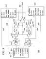
- FIG. 3is a simplified schematic of a basic single-stage level shifter.
- inputs to a high-side inverter 302 and a low-side inverter 308control the source voltages for an output inverter 314 .
- VDD 104is coupled to the V+ SRC connection of a first inverter block 302 whose V ⁇ SRC connection is coupled to a common voltage 304 which is often approximately midway between VDD 104 and VSS 106 .
- the input 306 to inverter 302operates typically switches between the levels of VDD 104 and common voltage 304 , though devices may be fabricated to accept inputs over other ranges.
- a second inverter block 308has the V+ SRC input coupled to the common voltage 304 and the V ⁇ SRC coupled to VSS 106 , so that its input 310 typically, though not necessarily, accepts a control input that switches between approximately VSS 106 and common 304 .
- the output 312 of inverter 302switches between about common 304 and VDD 104 , and is provided to the V+ SRC connection of a third, larger inverter block 314 whose V ⁇ SRC connection is coupled to the output 316 of the inverter 308 , which switches between about VSS 106 and common 304 . Accordingly, when a suitable logic low level (about common 304 ) is applied to input 306 , and a different suitable logic low level (about VSS 106 ) is applied to input 310 , outputs 312 and 316 go to VDD and common, respectively. Thus, inverter 314 has only a single supply voltage (VDD—common) disposed across its source connections.
- VDDsingle supply voltage
- output inverter 314again has only one supply voltage (common—VSS) disposed across its source connections.
- V+ SRC connection 312 and V ⁇ SRC connection 316 of the output inverter 314switches between VDD and common, respectively, for suitable logic low levels on inputs 306 and 310 , and common a VSS, respectively, for suitable logic high levels on inputs 306 and 310 .
- the input of the output inverter 314is coupled to common 304 , its output 318 goes to about VDD in the logic low input condition, and to about VSS in the logic high condition.
- Output 318is the primary output of this level shifter stage.
- the FETs in inverter block 314have the same breakdown voltage as do those in inverters 302 and 308 , and both are close to the greater of the first supply (VDD—common) or the second supply (common—VSS). Under such circumstances it is important that outputs 312 and 316 are never at VDD and VSS, respectively, and indeed it is important that the voltage difference across the outputs not exceed the greater of the two supply voltage magnitudes at any time either the P FET or the N FET of output inverter block 314 is conducting. Such overvoltage conditions may be avoided by the principles illustrated in the circuits of FIGS. 4-9 .
- FIGS. 4 and 5are signal transmit blocks that include a transmission gate and a clamp to common.
- Signal Transmit H 400 of FIG. 4is intended for operation with a “high” side signal between VDD and common.
- the transmission gateconsisting of P FET 402 and N FET 404 couples a signal between input I 406 and output O 408 when the control signals _X 410 and X 412 are logic low (common) and high (VDD) respectively.
- the signalis within a suitable voltage range, which in the exemplary embodiment is the same as the range of the control inputs 410 and 412 , i.e., between common and VDD.
- the control signals _ 410 and X 412are inverted to logic high (VDD) and low (common) respectively, the signal at I 406 is blocked, and the output O 408 is clamped down to common by N FET 414 .
- Signal Transmit L 500 of FIG. 5is intended for “low” side operation between common and VSS.
- the transmission gate consisting of N FET 502 and P FET 504couples a signal between input I 506 and output O 508 when the control signals _X 510 and X 512 are logic low (VSS) and high (common) respectively.
- the signalis within a suitable voltage range, which in the exemplary embodiment is the same as the range of the control inputs 510 and 512 , i.e., between VSS and common.
- the control signals _X 510 and X 512are inverted to logic high (common) and low (VSS) respectively, the signal at I 506 is blocked, and the output O 508 is clamped up to common by P FET 514 .
- FIGS. 6 and 7are both schematic diagrams of single stage differential output level shifters.
- the level shifter 600 of FIG. 6operates with a “high side” logic control input at IN_G 2 VD 602 , i.e., between common (low) and VDD (high).
- the level shifter 700 of FIG. 7operates with a “low side” logic control input at IN_VS 2 G 702 , i.e., between VSS (low) and common (high).
- the level shifter 600includes a non-inverting output OUT_VS 2 VD 604 that rises from VSS to VDD when the input IN_G 2 VD rises from common to VDD, and an inverted output OUT_VD 2 VS 606 that falls from VDD to VSS in response to the same input change.
- the two outputsare generated by two inverter trios configured similarly as the high-side inverter 302 , low-side inverter 308 and output inverter 314 of FIG. 3 .
- High-side inverter 608 , low-side inverter 610 and output inverter 612generate the non-inverting output OUT_VS 2 VD 604 .
- This outputis rendered non-inverting from the input by the additional high-side inverter 614 that inverts IN_G 2 VD for the input to inverter 608 .
- High-side inverter 616 , low-side inverter 618 and output inverter 620generate inverting output OUT_VD 2 VS, which, as in FIG. 3 , is inverting with respect to the input.
- the input to low-side inverter 610is provided by the inverting output OUT_VD 2 VS 606 .
- that output signalranges from VSS to VDD, so it is limited to the proper input range (VSS to common) by N FETs 622 and 624 .
- N FET 622couples the input of 610 to common 304
- N FET 624couples the input of 610 to VSS.
- the input to low-side inverter 618is provided by the non-inverting output OUT_VS 2 VD 604 , which is limited to the low-side input range by N FETs 626 and 628 .
- each half of level shifter 600differs from the circuit of FIG. 3 by virtue of an impedance Zs 630 in the connection to source supply VSS 106 .
- Zs 630serves to limit the value of the low-side supply during transitions from one state to another. Because there is little DC current flow, it has no impact on steady-state voltages. In conjunction with capacitors 632 and 634 (typically about 0.5 pF each), Zs 630 limits the transient voltage swings that would otherwise occur across the source supplies of the output inverters 612 and 620 , respectively.
- Capacitor 634causes the sink of inverter 620 to track its source, O_VD 2 G 638 , causing output OUT_VD 2 VS 606 to rise. In turn, that causes inverter 610 to drive toward VSS, which reinforces the movement toward VSS by O_VS 2 G that was previously caused by capacitor 632 as driven by inverter 608 . In the same manner, capacitor 632 enables inverter 612 to almost immediately switch toward VSS in response to a falling input at IN_G 2 VD 602 . That in turn causes inverter 618 to reinforce the rise toward ground of O_G 2 VS 640 that was previously caused by capacitor 634 driven by inverter 616 .
- Zs 630may serve a plurality of purposes. It may facilitate an ability of capacitors 632 and 634 to maintain the source voltage across output inverters 612 and 620 reasonably constant during the switching sequence. It also slows switching speed.
- Zsis simply a resistor of 5 k to 20 k ohms, but may have a resistance within an order of magnitude of 10,000 ohms.
- Zsmay have an inductive component, or even be primarily inductive, in which case the impedance magnitude should be determined at a transition frequency Ft that is 1/Ts, where Ts is the transition time from an input transition at, e.g., IN_G 2 VD 602 , to O_VS 2 G 642 .
- Tsmay alternatively be calculated as the time between other suitable voltage transitions.
- the magnitude of the impedance Zsshould be greater than 1000 ohms at Ft, or may be limited to being within an order of magnitude, or alternatively within a factor of 4, of 10,000 ohms at Ft.
- Zsmay, in fact, be an active FET device, with or without a second cascode device, configured to operate substantially as a limited current source during transitions.
- Zs 630is particularly useful when the VDD and VSS supplies (with respect to common) are asymmetric, i.e., have different magnitudes, in which case Zs should be disposed in series with the supply that is of larger magnitude.
- VDD and VSSare asymmetric in an exemplary embodiment: VSS is about ⁇ 3.4 V, while VDD is about +2.4 V, both with respect to common. Accordingly, in such embodiment Zs 630 is disposed in series with VSS.
- the single stage differential output level shifter 700 of FIG. 7operates quite similarly as level shifter 600 .
- input IN_VS 2 G 702directly drives low-side inverters 704 and 708 , the latter via extra low-side inverter 710 .
- low side output O_G 2 VS 712will switch first, closely followed (due to extra inverter 710 ) by low side output O_VS 2 G 714 .
- Capacitors 716 and 718(e.g., about 0.5 pF) will hold the source voltage substantially constant across the output inverters 720 and 722 , respectively. This in turn permits the output inverters to switch the outputs OUT_VS 2 VD 724 and OUT_VD 2 VS 726 .
- Zs 744(5 k to 20 k ohms, primarily resistive, in exemplary embodiments) may be disposed in series with a supply, particularly when VDD and VSS are asymmetric with respect to common.
- Zs 744may serve, for example, to facilitate the ability of the capacitors 716 and 718 to maintain constant source voltage for the output inverters during switching, particularly when the VDD and VSS supplies are asymmetric.
- Zs 744may take on any value as described above for Zs 630 , and may be replaced by a current limiting circuit.
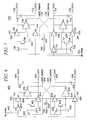
- FIG. 8schematically illustrates a two-stage differential output level shifter 800 .
- the first stage 802is a single stage differential output level shifter having outputs as indicated in the level shifters 600 and 700 of FIGS. 6 and 7 .
- level shifter 802employs the switching logic of the level shifter 600 .
- the level-shifted outputs of the first stage 802(OUT_VS 2 VD and OUT_VD 2 VS) are used only internally. Only the high-side and low-side outputs, including the inverted outputs O_VD 2 G and O_G 2 VS, respectively, and the non-inverted outputs O_G 2 VD and O_VS 2 G, respectively, are used.
- These signalsare coupled to a second stage of level shifter 800 via signal transmit blocks.
- the high-side outputsare coupled via Signal Transmit H blocks 806 and 808 , then via high-side inverters 810 and 812 , to produce high side signals Sa 814 and Sd 816 .
- These signalsare again inverted by higher power inverters 818 and 820 to produce VDa 822 and VDb 824 , which are V+ SRC connections for the highest power output inverters 826 and 828 , respectively.
- the outputs of those inverters 826 and 828are the final level shifted differential outputs OUT 830 and OUTX 832 of the two stage level shifter 800 .
- the low-side outputsare coupled to the second stage via Signal Transmit L blocks 834 and 836 , and then via low-side inverters 838 and 840 to establish signals Sb 842 and Sc 844 .
- Larger low-side inverters 846 and 848produce the low-side non-inverted and inverted outputs VSa 850 and VSb 852 , respectively.
- VSa 850 and VSb 852are the V ⁇ SRC connections for the output inverters 826 and 828 , respectively.
- V+ SRC or the V ⁇ SRC connection of an output inverteris at common 304 in every static state. If such connection at common voltage moves toward its particular supply rail (VDD for V+ SRC , VSS for V ⁇ SRC ) faster than the opposite source connection moves toward common, then the net voltage across the output inverter will increase above its static value. This can impair reliability if the FETs are operating near their voltage withstand capacity. To avoid such transient voltage spikes it is desired to ensure that whichever source supply (V+ SRC or V ⁇ SRC ) will be moving toward common voltage will be forced to substantially begin its transition before the opposite source is permitted to begin transitioning. This is accomplished in the level shifter 800 by means of the Signal Transmit blocks 806 , 808 and 834 , 836 .
- VDa 822When IN 804 is logic high, VDa 822 is at VDD, VSa 850 at common, VDb 824 at common and VSb 852 is at VSS. When IN 804 transitions to logic low, all of these voltages will change, but the transitions of VSa 850 and VDb 824 are delayed. They will change in response to the signal from Signal Transmit L block 834 and Signal Transmit H block 808 , respectively. However, signals VSb 852 (VSS) on X and Sc 844 (common) on _X initially disable Signal Transmit L block 834 , while signals VDa 822 (VDD) on X and Sa 814 (common) initially disable Signal Transmit H block 808 . VSb 852 and Sc 844 are permitted to change by Signal Transmit L block 836 , which is initially enabled by VSa 846 (common) on X and Sb 842 (VDD) on _X.
- VDa 822When IN 804 is logic low, VDa 822 is at common, VSa 850 at VSS, VDb 824 at VDD and VSb 852 is at common.
- the transitions of VDa 822 and VSb 852are delayed by the initial condition of Signal Transmit blocks 806 and 836 . These Signal Transmit blocks will not be enabled to transmit the new signal from the first stage 802 until VDb 824 and Sd 816 , as well as VSa 846 and Sb 842 , have substantially transitioned. In all cases, suitable transition threshold voltages should be selected to ensure that racing cannot permit voltage spikes across the source voltages of the output inverters 826 and 828 .
- level shifter 800initially disabled Signal Transmit blocks for one side of the level shifter (either the non-inverted OUT side, or the opposing OUTX side) are enabled by the transition of an output an on the opposite side. These signals are not available in single-ended (one sided) level shifters, so an alternative circuit is illustrated for such level shifters in FIG. 9 .
- a logic input 902 arbitrarily selected to accept inputs between VDD and commoncontrols the two stage single-ended level shifter 900 of FIG. 9 .
- the first stage(or front end) is a differential level shifter 904 , which may be implemented identically as the level shifter 600 of FIG. 6 , or in any other manner that will provide a high-side non-inverted output O_G 2 VD between common and VDD, and a low-side non-inverted output O_VS 2 G between VSS and common.
- additional inverters in both sidesaffect only the polarity of the net output OUT 906 from the large output inverter 908 .
- the small inverters 910 and 912produce inverted signals Sa 914 and Sb 916 , which are inverted by medium inverters 918 and 920 to produce higher power non-inverted signals VDa 922 and VSa 924 , which in turn are V+ SRC and V ⁇ SRC for the output inverter 908 .
- level shifter 926accepts a high-side input control from VDa 922 and thus may be implemented like level shifter 500 of FIG. 5
- level shifter 928accepts a low-side input control from VSa 924 and thus may be implemented like level shifter 600 of FIG. 6
- the low-side outputs of level shifter 926 , non-inverting output O_VS 2 G 930 and inverting output O_G 2 VS 932are coupled respectively to X and _X of low-side Signal Transmit L block 934 .
- level shifter 928The high-side outputs of level shifter 928 , non-inverting O_G 2 VD 936 and inverting O_VD 2 G 938 are coupled respectively to X and _X of Signal Transmit H block 940 .
- VDa 922when VDa 922 is at common, it is prevented from switching toward VDD until after a rising VSa enables Signal Transmit H block 940 via level shifter 928 ; and conversely, when VSa 924 is at common, it is prevented from switching toward VSS until after a falling VDa 922 enables Signal Transmit L block 934 via level shifter 926 .
- level shifter 900may be even more resistant to excess voltage spikes across its output inverter 908 than is level shifter 800 , but significant additional circuitry is used to ensure suitable timing.
- Level shifter input voltage rangesare typically between VDD and common, or between common and VSS, but the level shifters can readily be modified to accept control input over a nearly arbitrary input voltage range.
- Input circuitry of level shifter 600 of FIG. 6accepts control input voltages on the high side (VDD to common), while input circuitry of level shifter 700 of FIG. 7 accepts control input voltages on the low side (common to VSS).
- input range limiting circuitrye.g., such as represented by FETs 622 and 624 of FIG. 6
- standard engineering knowledgea skilled person will readily be able to implement embodiments of any level shifter described herein to accept inputs within another input voltage range.
- Such input voltage rangecan be made nearly arbitrary by use of range limiting circuitry, plus amplifying circuitry if needed.
- a level shifterby definition controls an output over a different output voltage range than the input voltage range, no particular restriction on the relationship between input and output voltage ranges is necessary.
- FIGS. 8 and 9may be replaced by any suitable logic function that achieves substantially the same effect.
- Different level shifter circuitsmay be used in place of level shifter stages 802 , 902 , 926 and 928 , and the inverter blocks may be implemented differently.
- circuits illustrated and described hereinare only exemplary, and should be interpreted as equally describing such alternatives as may be reasonably seen to be analogous by a person of skill in the art, whether by present knowledge common to such skilled persons, or in the future in view of unforeseen but readily-applied alternatives then known to such skilled persons.
Landscapes
- Engineering & Computer Science (AREA)
- Computer Hardware Design (AREA)
- Physics & Mathematics (AREA)
- Computing Systems (AREA)
- General Engineering & Computer Science (AREA)
- Mathematical Physics (AREA)
- Logic Circuits (AREA)
Abstract
Description
Claims (21)
Priority Applications (1)
| Application Number | Priority Date | Filing Date | Title |
|---|---|---|---|
| US12/460,442US9030248B2 (en) | 2008-07-18 | 2009-07-17 | Level shifter with output spike reduction |
Applications Claiming Priority (2)
| Application Number | Priority Date | Filing Date | Title |
|---|---|---|---|
| US13527808P | 2008-07-18 | 2008-07-18 | |
| US12/460,442US9030248B2 (en) | 2008-07-18 | 2009-07-17 | Level shifter with output spike reduction |
Publications (2)
| Publication Number | Publication Date |
|---|---|
| US20100033226A1 US20100033226A1 (en) | 2010-02-11 |
| US9030248B2true US9030248B2 (en) | 2015-05-12 |
Family
ID=41652339
Family Applications (1)
| Application Number | Title | Priority Date | Filing Date |
|---|---|---|---|
| US12/460,442Active2031-04-26US9030248B2 (en) | 2008-07-18 | 2009-07-17 | Level shifter with output spike reduction |
Country Status (1)
| Country | Link |
|---|---|
| US (1) | US9030248B2 (en) |
Cited By (12)
| Publication number | Priority date | Publication date | Assignee | Title |
|---|---|---|---|---|
| US20150123638A1 (en)* | 2013-11-07 | 2015-05-07 | Texas Instruments Deutschland Gmbh | Startup clamp circuit for non-complimentary differential pair in dcdc converter system |
| US9190902B2 (en) | 2003-09-08 | 2015-11-17 | Peregrine Semiconductor Corporation | Low noise charge pump method and apparatus |
| US9264053B2 (en) | 2011-01-18 | 2016-02-16 | Peregrine Semiconductor Corporation | Variable frequency charge pump |
| US9354654B2 (en) | 2011-05-11 | 2016-05-31 | Peregrine Semiconductor Corporation | High voltage ring pump with inverter stages and voltage boosting stages |
| US9429969B2 (en) | 2008-07-18 | 2016-08-30 | Peregrine Semiconductor Corporation | Low-noise high efficiency bias generation circuits and method |
| US9660590B2 (en) | 2008-07-18 | 2017-05-23 | Peregrine Semiconductor Corporation | Low-noise high efficiency bias generation circuits and method |
| US10018687B2 (en) | 2013-08-15 | 2018-07-10 | Texas Instruments Incorporated | Integrated fluxgate magnetic sensor and excitation circuitry |
| US10523205B1 (en)* | 2018-10-19 | 2019-12-31 | Taiwan Semiconductor Manufacturing Company Ltd. | Buffering device and method of controlling buffering device |
| US11092656B2 (en) | 2015-05-12 | 2021-08-17 | Texas Instruments Incorporated | Fluxgate magnetic field detection method and circuit |
| US11152917B1 (en)* | 2020-05-28 | 2021-10-19 | Analog Devices International Unlimited Company | Multi-level buffers for biasing of radio frequency switches |
| US20230006652A1 (en)* | 2021-07-05 | 2023-01-05 | Realtek Semiconductor Corporation | Transmission-end impedance matching circuit |
| US12040794B2 (en) | 2021-09-14 | 2024-07-16 | Samsung Electronics Co., Ltd. | Semiconductor integrated circuits that support enhanced signal multiplexing operations for I/O buffers |
Families Citing this family (2)
| Publication number | Priority date | Publication date | Assignee | Title |
|---|---|---|---|---|
| EP2421132A2 (en) | 2008-07-18 | 2012-02-22 | Peregrine Semiconductor Corporation | Charge pump with a plurality of transfer control switches |
| US9589642B2 (en)* | 2014-08-07 | 2017-03-07 | Macronix International Co., Ltd. | Level shifter and decoder for memory |
Citations (133)
| Publication number | Priority date | Publication date | Assignee | Title |
|---|---|---|---|---|
| US3646361A (en) | 1970-10-16 | 1972-02-29 | Hughes Aircraft Co | High-speed sample and hold signal level comparator |
| US3995228A (en) | 1975-09-26 | 1976-11-30 | Threshold Corporation | Active bias circuit for operating push-pull amplifiers in class A mode |
| US4158182A (en) | 1978-07-31 | 1979-06-12 | Harris Corporation | Low noise oscillator circuit |
| JPS5575348U (en) | 1978-11-20 | 1980-05-24 | ||
| US4316101A (en) | 1978-11-30 | 1982-02-16 | Licentia-Patent-Verwaltungs-G.M.B.H. | Circuit for switching and transmitting alternating voltages |
| US4374357A (en) | 1981-07-27 | 1983-02-15 | Motorola, Inc. | Switched capacitor precision current source |
| US4390798A (en) | 1979-11-22 | 1983-06-28 | Fujitsu Limited | Bias-voltage generator |
| USRE31749E (en) | 1975-09-03 | 1984-11-27 | Hitachi, Ltd. | Class B FET amplifier circuit |
| US4638184A (en) | 1983-09-22 | 1987-01-20 | Oki Electric Industry Co., Ltd. | CMOS bias voltage generating circuit |
| US4736169A (en) | 1986-09-29 | 1988-04-05 | Hughes Aircraft Company | Voltage controlled oscillator with frequency sensitivity control |
| US4739191A (en) | 1981-04-27 | 1988-04-19 | Signetics Corporation | Depletion-mode FET for the regulation of the on-chip generated substrate bias voltage |
| US4746960A (en) | 1987-07-27 | 1988-05-24 | General Motors Corporation | Vertical depletion-mode j-MOSFET |
| US4891609A (en) | 1987-12-22 | 1990-01-02 | U.S. Philips Corporation | Ring oscillator |
| US5023494A (en) | 1989-10-20 | 1991-06-11 | Raytheon Company | High isolation passive switch |
| US5061907A (en) | 1991-01-17 | 1991-10-29 | National Semiconductor Corporation | High frequency CMOS VCO with gain constant and duty cycle compensation |
| JPH0434980Y2 (en) | 1986-06-30 | 1992-08-19 | ||
| JPH04334105A (en) | 1991-05-08 | 1992-11-20 | Sharp Corp | Current source circuit |
| US5182529A (en) | 1992-03-06 | 1993-01-26 | Micron Technology, Inc. | Zero crossing-current ring oscillator for substrate charge pump |
| US5208557A (en) | 1992-02-18 | 1993-05-04 | Texas Instruments Incorporated | Multiple frequency ring oscillator |
| US5274343A (en) | 1991-08-06 | 1993-12-28 | Raytheon Company | Plural switch circuits having RF propagation networks and RF terminations |
| US5317181A (en) | 1992-09-10 | 1994-05-31 | United Technologies Corporation | Alternative body contact for fully-depleted silicon-on-insulator transistors |
| JPH06314985A (en) | 1993-04-28 | 1994-11-08 | Nec Corp | Portable radio device |
| JPH06334506A (en) | 1993-05-21 | 1994-12-02 | Sony Corp | Switch for signal switching |
| US5446418A (en) | 1992-11-06 | 1995-08-29 | Mitsubishi Denki Kabushiki Kaisha | Ring oscillator and constant voltage generation circuit |
| US5483195A (en) | 1994-10-20 | 1996-01-09 | Northern Telecom Limited | Second generation low noise microwave voltage controlled oscillator |
| US5493249A (en) | 1993-12-06 | 1996-02-20 | Micron Technology, Inc. | System powered with inter-coupled charge pumps |
| US5528245A (en) | 1995-02-10 | 1996-06-18 | Applied Concepts, Inc. | Police traffic radar using double balanced mixer for even order harmonic suppression |
| JPH08307305A (en) | 1994-08-30 | 1996-11-22 | Matsushita Electric Ind Co Ltd | Transmission / reception circuit of communication radio, semiconductor integrated circuit device, and communication radio |
| JPH09200021A (en) | 1996-01-22 | 1997-07-31 | Mitsubishi Electric Corp | Integrated circuit |
| US5670907A (en) | 1995-03-14 | 1997-09-23 | Lattice Semiconductor Corporation | VBB reference for pumped substrates |
| US5694308A (en) | 1995-07-03 | 1997-12-02 | Motorola, Inc. | Method and apparatus for regulated low voltage charge pump |
| US5729039A (en) | 1994-06-29 | 1998-03-17 | International Business Machines Corporation | SOI transistor having a self-aligned body contact |
| US5734291A (en) | 1996-03-11 | 1998-03-31 | Telcom Semiconductor, Inc. | Power saving technique for battery powered devices |
| JPH1093471A (en) | 1996-09-11 | 1998-04-10 | Murata Mfg Co Ltd | Signal changeover switch |
| US5793246A (en) | 1995-11-08 | 1998-08-11 | Altera Corporation | High voltage pump scheme incorporating an overlapping clock |
| JPH10242829A (en) | 1997-02-24 | 1998-09-11 | Sanyo Electric Co Ltd | Switch circuit device |
| JPH10242477A (en) | 1996-12-26 | 1998-09-11 | Hitachi Ltd | Semiconductor device and manufacturing method thereof |
| US5808505A (en) | 1993-05-25 | 1998-09-15 | Nec Corporation | Substrate biasing circuit having controllable ring oscillator |
| US5812939A (en) | 1995-08-10 | 1998-09-22 | Sony Corporation | Switch semiconductor integrated circuit and communication terminal device |
| US5818289A (en) | 1996-07-18 | 1998-10-06 | Micron Technology, Inc. | Clocking scheme and charge transfer switch for increasing the efficiency of a charge pump or other circuit |
| US5818766A (en) | 1997-03-05 | 1998-10-06 | Integrated Silicon Solution Inc. | Drain voltage pump circuit for nonvolatile memory device |
| US5864328A (en) | 1995-09-01 | 1999-01-26 | Sharp Kabushiki Kaisha | Driving method for a liquid crystal display apparatus |
| US5874849A (en) | 1996-07-19 | 1999-02-23 | Texas Instruments Incorporated | Low voltage, high current pump for flash memory |
| US5892400A (en) | 1995-12-15 | 1999-04-06 | Anadigics, Inc. | Amplifier using a single polarity power supply and including depletion mode FET and negative voltage generator |
| JPH11136111A (en) | 1997-10-30 | 1999-05-21 | Sony Corp | High frequency circuit |
| US5917362A (en) | 1996-01-29 | 1999-06-29 | Sony Corporation | Switching circuit |
| US5959335A (en) | 1998-09-23 | 1999-09-28 | International Business Machines Corporation | Device design for enhanced avalanche SOI CMOS |
| US6020781A (en) | 1996-12-27 | 2000-02-01 | Fujitsu Limited | Step-up circuit using two frequencies |
| US6064872A (en) | 1991-03-12 | 2000-05-16 | Watkins-Johnson Company | Totem pole mixer having grounded serially connected stacked FET pair |
| US6064275A (en) | 1996-04-22 | 2000-05-16 | Mitsubishi Denki Kabushiki Kaisha | Internal voltage generation circuit having ring oscillator whose frequency changes inversely with power supply voltage |
| JP2000166220A (en) | 1998-09-22 | 2000-06-16 | Sharp Corp | Power supply circuit Display device and electronic device using the same |
| US6081165A (en) | 1997-07-25 | 2000-06-27 | Texas Instruments Incorporated | Ring oscillator |
| US6087968A (en) | 1997-04-16 | 2000-07-11 | U.S. Philips Corporation | Analog to digital converter comprising an asynchronous sigma delta modulator and decimating digital filter |
| US6122185A (en) | 1997-07-22 | 2000-09-19 | Seiko Instruments R&D Center Inc. | Electronic apparatus |
| US6169444B1 (en) | 1999-07-15 | 2001-01-02 | Maxim Integrated Products, Inc. | Pulse frequency operation of regulated charge pumps |
| US6188590B1 (en) | 1996-12-18 | 2001-02-13 | Macronix International Co., Ltd. | Regulator system for charge pump circuits |
| JP2001051758A (en) | 1999-08-04 | 2001-02-23 | Hitachi Ltd | Data receiving circuit for polarized RTZ signal |
| US6195307B1 (en) | 1997-02-26 | 2001-02-27 | Kabushiki Kaisha Toshiba | Booster circuit and semiconductor memory device having the same |
| USRE37124E1 (en) | 1993-04-30 | 2001-04-03 | Stmicroelectronics Limited | Ring oscillator using current mirror inverter stages |
| JP2001119281A (en) | 1999-10-19 | 2001-04-27 | Nippon Telegr & Teleph Corp <Ntt> | Selection circuit and logic circuit using the same |
| US6226206B1 (en) | 1998-03-12 | 2001-05-01 | Nec Corporation | Semiconductor memory device including boost circuit |
| US6249446B1 (en) | 2000-08-23 | 2001-06-19 | Intersil Americas Inc. | Cascadable, high efficiency charge pump circuit and related methods |
| US6297687B1 (en) | 1998-08-11 | 2001-10-02 | Oki Electric Industry Co., Ltd. | Drive control circuit of charged pump circuit |
| US20010031518A1 (en) | 1999-10-25 | 2001-10-18 | Samsung Electronics,Co. Ltd | Soi semiconductor integrated circuit for eliminating floating body effects in soi mosfets and method of fabricating the same |
| US6308047B1 (en) | 1996-08-05 | 2001-10-23 | Mitsubishi Denki Kabushiki Kaisha | Radio-frequency integrated circuit for a radio-frequency wireless transmitter-receiver with reduced influence by radio-frequency power leakage |
| US6337594B1 (en) | 1998-06-17 | 2002-01-08 | Hynix Semiconductor, Inc. | Charge pump circuit |
| US6400211B1 (en) | 2000-09-19 | 2002-06-04 | Rohm Co., Ltd. | DC/DC converter |
| US6414863B1 (en) | 2001-08-30 | 2002-07-02 | Texas Instruments Incorporated | Frequency control circuit for unregulated inductorless DC/DC converters |
| US6429632B1 (en) | 2000-02-11 | 2002-08-06 | Micron Technology, Inc. | Efficient CMOS DC-DC converters based on switched capacitor power supplies with inductive current limiters |
| US6429723B1 (en) | 1999-11-18 | 2002-08-06 | Texas Instruments Incorporated | Integrated circuit with charge pump and method |
| US6429730B2 (en) | 1999-04-29 | 2002-08-06 | International Business Machines Corporation | Bias circuit for series connected decoupling capacitors |
| US20020115244A1 (en) | 2000-08-11 | 2002-08-22 | Sung-Bae Park | SOI MOSFET having body contact for preventing floating body effect and method of fabricating the same |
| US6452232B1 (en) | 1998-12-03 | 2002-09-17 | Sharp Kabushiki Kaisha | Semiconductor device having SOI structure and manufacturing method thereof |
| US20020140412A1 (en) | 2001-01-26 | 2002-10-03 | True Circuits, Inc. | Programmable current mirror |
| US6486729B2 (en) | 2000-05-24 | 2002-11-26 | Kabushiki Kaisha Toshiba | Potential detector and semiconductor integrated circuit |
| US6504213B1 (en) | 1999-07-27 | 2003-01-07 | Seiko Epson Corporation | SOI-structure field-effect transistor and method of manufacturing the same |
| US20030034849A1 (en) | 2001-08-16 | 2003-02-20 | Sanduleanu Mihai Adrian Tiberiu | Ring oscillator stage |
| US6537861B1 (en) | 1998-08-29 | 2003-03-25 | International Business Machines Corporation | SOI transistor with body contact and method of forming same |
| US6559689B1 (en) | 2000-10-02 | 2003-05-06 | Allegro Microsystems, Inc. | Circuit providing a control voltage to a switch and including a capacitor |
| US20030141543A1 (en) | 2002-01-31 | 2003-07-31 | International Business Machines Corporation | Body contact mosfet |
| US6617933B2 (en) | 2000-09-29 | 2003-09-09 | Mitsubishi Denki Kabushiki Kaisha | VCO circuit with wide output frequency range and PLL circuit with the VCO circuit |
| US20030201494A1 (en) | 2002-04-25 | 2003-10-30 | Mitsubishi Denki Kabushiki Kaisha | Semiconductor device and method of manufacturing the same |
| US6653697B2 (en) | 2001-03-27 | 2003-11-25 | Matsushita Electric Industrial Co., Ltd. | High frequency switch circuit and communications terminal using the same |
| US6677641B2 (en) | 2001-10-17 | 2004-01-13 | Fairchild Semiconductor Corporation | Semiconductor structure with improved smaller forward voltage loss and higher blocking capability |
| US6714065B2 (en) | 2001-10-26 | 2004-03-30 | Renesas Technology Corp. | Semiconductor device including power supply circuit conducting charge pumping operation |
| US20040061130A1 (en) | 2000-03-30 | 2004-04-01 | Mayumi Morizuka | High electron mobility transistor and method of manufacturing the same |
| US6717458B1 (en) | 2001-12-03 | 2004-04-06 | National Semiconductor Corporation | Method and apparatus for a DC-DC charge pump voltage converter-regulator circuit |
| JP2004147175A (en) | 2002-10-25 | 2004-05-20 | Renesas Technology Corp | Semiconductor device |
| US20040129975A1 (en) | 2002-12-06 | 2004-07-08 | Nec Corporation | Semiconductor device and method for manufacturing the same |
| US6774704B2 (en)* | 2002-10-28 | 2004-08-10 | Tower Semiconductor Ltd. | Control circuit for selecting the greater of two voltage signals |
| US6784737B2 (en) | 2001-12-17 | 2004-08-31 | Intel Corporation | Voltage multiplier circuit |
| US6788130B2 (en) | 2002-09-25 | 2004-09-07 | Texas Instruments Incorporated | Efficient charge pump capable of high voltage operation |
| US6801076B1 (en) | 2000-04-28 | 2004-10-05 | Micron Technology, Inc. | High output high efficiency low voltage charge pump |
| US6804502B2 (en)* | 2001-10-10 | 2004-10-12 | Peregrine Semiconductor Corporation | Switch circuit and method of switching radio frequency signals |
| US20040204013A1 (en) | 2002-12-23 | 2004-10-14 | Qing Ma | Communication unit and switch unit |
| US6816016B2 (en) | 2000-08-10 | 2004-11-09 | Tropian, Inc. | High-efficiency modulating RF amplifier |
| US6819938B2 (en) | 2001-06-26 | 2004-11-16 | Qualcomm Incorporated | System and method for power control calibration and a wireless communication device |
| US20050052220A1 (en) | 2003-09-08 | 2005-03-10 | Burgener Mark L. | Low noise charge pump method and apparatus |
| US6871059B1 (en) | 1999-06-16 | 2005-03-22 | Skyworks Solutions, Inc. | Passive balun FET mixer |
| US6879502B2 (en) | 2002-06-13 | 2005-04-12 | Seiko Instruments Inc. | Power source inverter circuit |
| US20050077564A1 (en) | 2003-10-09 | 2005-04-14 | Micron Technology, Inc. | Fully depleted silicon-on-insulator CMOS logic |
| US6891234B1 (en) | 2004-01-07 | 2005-05-10 | Acorn Technologies, Inc. | Transistor with workfunction-induced charge layer |
| US20050121699A1 (en) | 2003-12-08 | 2005-06-09 | Xiangdong Chen | Dynamic threshold voltage MOSFET on SOI |
| US6947720B2 (en) | 2000-10-17 | 2005-09-20 | Rf Micro Devices, Inc. | Low noise mixer circuit with improved gain |
| US7023260B2 (en) | 2003-06-30 | 2006-04-04 | Matrix Semiconductor, Inc. | Charge pump circuit incorporating corresponding parallel charge pump stages and method therefor |
| US20060194558A1 (en) | 2005-02-03 | 2006-08-31 | Kelly Dylan J | Canceling harmonics in semiconductor RF switches |
| US7109532B1 (en) | 2003-12-23 | 2006-09-19 | Lee Zachary K | High Ion/Ioff SOI MOSFET using body voltage control |
| US20060284670A1 (en) | 2005-06-21 | 2006-12-21 | Salem Eid | Neutralization Techniques for differential low noise amplifiers |
| JP2006352326A (en) | 2005-06-14 | 2006-12-28 | Toyota Motor Corp | Differential amplifier circuit |
| US7161197B2 (en) | 2004-05-31 | 2007-01-09 | Matsushita Electric Industrial Co., Ltd. | RF switching circuit for use in mobile communication systems |
| US20070045697A1 (en) | 2005-08-31 | 2007-03-01 | International Business Machines Corporation | Body-contacted semiconductor structures and methods of fabricating such body-contacted semiconductor structures |
| US7212788B2 (en) | 2002-08-13 | 2007-05-01 | Atheros Communications, Inc. | Method and apparatus for signal power loss reduction in RF communication systems |
| US20070146064A1 (en) | 2005-12-28 | 2007-06-28 | Takashi Morie | Transconductor, integrator, and filter circuit |
| US20070279120A1 (en) | 2003-12-15 | 2007-12-06 | Infineon Technologies Ag | Noise-Reducing Transistor Arrangement, Integrated Circuit, and Method for Reducing the Noise of Field Effect Transistors |
| US20080007980A1 (en) | 2005-07-05 | 2008-01-10 | Nec Electronics Corporation | Power supply apparatus including charge-pump type step-up circuit having different discharging time constants |
| US20080030237A1 (en) | 2006-08-04 | 2008-02-07 | Stmicroelectronics S.R.L. | Signal-processing circuit, in particular operating as a rectifier and peak detector, with active elements and differential inputs |
| US20080076371A1 (en) | 2005-07-11 | 2008-03-27 | Alexander Dribinsky | Circuit and method for controlling charge injection in radio frequency switches |
| US7391282B2 (en) | 2004-11-17 | 2008-06-24 | Matsushita Electric Industrial Co., Ltd. | Radio-frequency switch circuit and semiconductor device |
| US20080272845A1 (en) | 2007-05-02 | 2008-11-06 | Micron Technology, Inc. | Operational transconductance amplifier (ota) |
| US7515882B2 (en) | 2002-12-17 | 2009-04-07 | Kelcourse Mark F | Apparatus, methods and articles of manufacture for a multi-band switch |
| US7546089B2 (en) | 2004-12-23 | 2009-06-09 | Triquint Semiconductor, Inc. | Switchable directional coupler for use with RF devices |
| WO2010008586A2 (en) | 2008-07-18 | 2010-01-21 | Peregrine Semiconductor Corporation | Low-noise high efficiency bias generation circuits and method |
| US7659152B2 (en) | 2002-08-29 | 2010-02-09 | Micron Technology, Inc. | Localized biasing for silicon on insulator structures |
| US7733156B2 (en) | 2003-09-04 | 2010-06-08 | Infineon Technologies Ag | Transistor arrangement, integrated circuit and method for operating field effect transistors |
| US7796969B2 (en) | 2001-10-10 | 2010-09-14 | Peregrine Semiconductor Corporation | Symmetrically and asymmetrically stacked transistor group RF switch |
| US7910993B2 (en) | 2005-07-11 | 2011-03-22 | Peregrine Semiconductor Corporation | Method and apparatus for use in improving linearity of MOSFET's using an accumulated charge sink |
| US7982265B2 (en) | 2003-05-20 | 2011-07-19 | Fairchild Semiconductor Corporation | Trenched shield gate power semiconductor devices and methods of manufacture |
| US20120038344A1 (en) | 2010-08-06 | 2012-02-16 | Tae Youn Kim | Low-Noise High Efficiency Bias Generation Circuits and Method |
| US8138815B2 (en)* | 2007-10-19 | 2012-03-20 | Infineon Technologies Ag | Level converter |
| DE102005039138B4 (en) | 2005-08-18 | 2012-07-12 | Infineon Technologies Ag | By means of a resistor programmable and a reference current source having circuit |
| US8441299B2 (en) | 2010-01-28 | 2013-05-14 | Peregrine Semiconductor Corporation | Dual path level shifter |
| US8686787B2 (en) | 2011-05-11 | 2014-04-01 | Peregrine Semiconductor Corporation | High voltage ring pump with inverter stages and voltage boosting stages |
| US20150002195A1 (en) | 2011-01-18 | 2015-01-01 | Peregrine Semiconductor Corporation | Variable Frequency Charge Pump |
- 2009
- 2009-07-17USUS12/460,442patent/US9030248B2/enactiveActive
Patent Citations (158)
| Publication number | Priority date | Publication date | Assignee | Title |
|---|---|---|---|---|
| US3646361A (en) | 1970-10-16 | 1972-02-29 | Hughes Aircraft Co | High-speed sample and hold signal level comparator |
| USRE31749E (en) | 1975-09-03 | 1984-11-27 | Hitachi, Ltd. | Class B FET amplifier circuit |
| US3995228A (en) | 1975-09-26 | 1976-11-30 | Threshold Corporation | Active bias circuit for operating push-pull amplifiers in class A mode |
| US4158182A (en) | 1978-07-31 | 1979-06-12 | Harris Corporation | Low noise oscillator circuit |
| JPS5575348U (en) | 1978-11-20 | 1980-05-24 | ||
| US4316101A (en) | 1978-11-30 | 1982-02-16 | Licentia-Patent-Verwaltungs-G.M.B.H. | Circuit for switching and transmitting alternating voltages |
| US4390798A (en) | 1979-11-22 | 1983-06-28 | Fujitsu Limited | Bias-voltage generator |
| US4739191A (en) | 1981-04-27 | 1988-04-19 | Signetics Corporation | Depletion-mode FET for the regulation of the on-chip generated substrate bias voltage |
| US4374357A (en) | 1981-07-27 | 1983-02-15 | Motorola, Inc. | Switched capacitor precision current source |
| US4638184A (en) | 1983-09-22 | 1987-01-20 | Oki Electric Industry Co., Ltd. | CMOS bias voltage generating circuit |
| JPH0434980Y2 (en) | 1986-06-30 | 1992-08-19 | ||
| US4736169A (en) | 1986-09-29 | 1988-04-05 | Hughes Aircraft Company | Voltage controlled oscillator with frequency sensitivity control |
| US4746960A (en) | 1987-07-27 | 1988-05-24 | General Motors Corporation | Vertical depletion-mode j-MOSFET |
| US4891609A (en) | 1987-12-22 | 1990-01-02 | U.S. Philips Corporation | Ring oscillator |
| US5023494A (en) | 1989-10-20 | 1991-06-11 | Raytheon Company | High isolation passive switch |
| US5023494B1 (en) | 1989-10-20 | 1992-10-27 | Raytheon Co | |
| US5061907A (en) | 1991-01-17 | 1991-10-29 | National Semiconductor Corporation | High frequency CMOS VCO with gain constant and duty cycle compensation |
| US6064872A (en) | 1991-03-12 | 2000-05-16 | Watkins-Johnson Company | Totem pole mixer having grounded serially connected stacked FET pair |
| JPH04334105A (en) | 1991-05-08 | 1992-11-20 | Sharp Corp | Current source circuit |
| US5274343A (en) | 1991-08-06 | 1993-12-28 | Raytheon Company | Plural switch circuits having RF propagation networks and RF terminations |
| US5208557A (en) | 1992-02-18 | 1993-05-04 | Texas Instruments Incorporated | Multiple frequency ring oscillator |
| US5182529A (en) | 1992-03-06 | 1993-01-26 | Micron Technology, Inc. | Zero crossing-current ring oscillator for substrate charge pump |
| US5317181A (en) | 1992-09-10 | 1994-05-31 | United Technologies Corporation | Alternative body contact for fully-depleted silicon-on-insulator transistors |
| US5446418A (en) | 1992-11-06 | 1995-08-29 | Mitsubishi Denki Kabushiki Kaisha | Ring oscillator and constant voltage generation circuit |
| JPH06314985A (en) | 1993-04-28 | 1994-11-08 | Nec Corp | Portable radio device |
| EP0622901B1 (en) | 1993-04-28 | 1999-02-03 | Nec Corporation | Signal processing circuit and control method with switch capable of reducing insertion loss |
| US5554892A (en) | 1993-04-28 | 1996-09-10 | Nec Corproation | Signal processing circuit for switch capable of reducing insertion loss |
| USRE37124E1 (en) | 1993-04-30 | 2001-04-03 | Stmicroelectronics Limited | Ring oscillator using current mirror inverter stages |
| JPH06334506A (en) | 1993-05-21 | 1994-12-02 | Sony Corp | Switch for signal switching |
| US5808505A (en) | 1993-05-25 | 1998-09-15 | Nec Corporation | Substrate biasing circuit having controllable ring oscillator |
| US5493249A (en) | 1993-12-06 | 1996-02-20 | Micron Technology, Inc. | System powered with inter-coupled charge pumps |
| US5729039A (en) | 1994-06-29 | 1998-03-17 | International Business Machines Corporation | SOI transistor having a self-aligned body contact |
| JPH08307305A (en) | 1994-08-30 | 1996-11-22 | Matsushita Electric Ind Co Ltd | Transmission / reception circuit of communication radio, semiconductor integrated circuit device, and communication radio |
| US5483195A (en) | 1994-10-20 | 1996-01-09 | Northern Telecom Limited | Second generation low noise microwave voltage controlled oscillator |
| US5528245A (en) | 1995-02-10 | 1996-06-18 | Applied Concepts, Inc. | Police traffic radar using double balanced mixer for even order harmonic suppression |
| US5670907A (en) | 1995-03-14 | 1997-09-23 | Lattice Semiconductor Corporation | VBB reference for pumped substrates |
| US5694308A (en) | 1995-07-03 | 1997-12-02 | Motorola, Inc. | Method and apparatus for regulated low voltage charge pump |
| US5812939A (en) | 1995-08-10 | 1998-09-22 | Sony Corporation | Switch semiconductor integrated circuit and communication terminal device |
| US5864328A (en) | 1995-09-01 | 1999-01-26 | Sharp Kabushiki Kaisha | Driving method for a liquid crystal display apparatus |
| US5793246A (en) | 1995-11-08 | 1998-08-11 | Altera Corporation | High voltage pump scheme incorporating an overlapping clock |
| US5892400A (en) | 1995-12-15 | 1999-04-06 | Anadigics, Inc. | Amplifier using a single polarity power supply and including depletion mode FET and negative voltage generator |
| JPH09200021A (en) | 1996-01-22 | 1997-07-31 | Mitsubishi Electric Corp | Integrated circuit |
| US5878331A (en) | 1996-01-22 | 1999-03-02 | Mitsubishi Denki Kabushiki Kaisha | Integrated circuit |
| US5917362A (en) | 1996-01-29 | 1999-06-29 | Sony Corporation | Switching circuit |
| US5734291A (en) | 1996-03-11 | 1998-03-31 | Telcom Semiconductor, Inc. | Power saving technique for battery powered devices |
| US6064275A (en) | 1996-04-22 | 2000-05-16 | Mitsubishi Denki Kabushiki Kaisha | Internal voltage generation circuit having ring oscillator whose frequency changes inversely with power supply voltage |
| US5818289A (en) | 1996-07-18 | 1998-10-06 | Micron Technology, Inc. | Clocking scheme and charge transfer switch for increasing the efficiency of a charge pump or other circuit |
| US5874849A (en) | 1996-07-19 | 1999-02-23 | Texas Instruments Incorporated | Low voltage, high current pump for flash memory |
| US6308047B1 (en) | 1996-08-05 | 2001-10-23 | Mitsubishi Denki Kabushiki Kaisha | Radio-frequency integrated circuit for a radio-frequency wireless transmitter-receiver with reduced influence by radio-frequency power leakage |
| JPH1093471A (en) | 1996-09-11 | 1998-04-10 | Murata Mfg Co Ltd | Signal changeover switch |
| US6188590B1 (en) | 1996-12-18 | 2001-02-13 | Macronix International Co., Ltd. | Regulator system for charge pump circuits |
| JPH10242477A (en) | 1996-12-26 | 1998-09-11 | Hitachi Ltd | Semiconductor device and manufacturing method thereof |
| US6020781A (en) | 1996-12-27 | 2000-02-01 | Fujitsu Limited | Step-up circuit using two frequencies |
| US5945867A (en) | 1997-02-24 | 1999-08-31 | Sanyo Electric Co., Ltd. | Switch circuit device |
| JPH10242829A (en) | 1997-02-24 | 1998-09-11 | Sanyo Electric Co Ltd | Switch circuit device |
| US6195307B1 (en) | 1997-02-26 | 2001-02-27 | Kabushiki Kaisha Toshiba | Booster circuit and semiconductor memory device having the same |
| US5818766A (en) | 1997-03-05 | 1998-10-06 | Integrated Silicon Solution Inc. | Drain voltage pump circuit for nonvolatile memory device |
| US6087968A (en) | 1997-04-16 | 2000-07-11 | U.S. Philips Corporation | Analog to digital converter comprising an asynchronous sigma delta modulator and decimating digital filter |
| US6122185A (en) | 1997-07-22 | 2000-09-19 | Seiko Instruments R&D Center Inc. | Electronic apparatus |
| US6081165A (en) | 1997-07-25 | 2000-06-27 | Texas Instruments Incorporated | Ring oscillator |
| JPH11136111A (en) | 1997-10-30 | 1999-05-21 | Sony Corp | High frequency circuit |
| US6563366B1 (en) | 1997-10-30 | 2003-05-13 | Sony Corporation | High-frequency Circuit |
| US6226206B1 (en) | 1998-03-12 | 2001-05-01 | Nec Corporation | Semiconductor memory device including boost circuit |
| US6337594B1 (en) | 1998-06-17 | 2002-01-08 | Hynix Semiconductor, Inc. | Charge pump circuit |
| US6297687B1 (en) | 1998-08-11 | 2001-10-02 | Oki Electric Industry Co., Ltd. | Drive control circuit of charged pump circuit |
| US6537861B1 (en) | 1998-08-29 | 2003-03-25 | International Business Machines Corporation | SOI transistor with body contact and method of forming same |
| JP2000166220A (en) | 1998-09-22 | 2000-06-16 | Sharp Corp | Power supply circuit Display device and electronic device using the same |
| US5959335A (en) | 1998-09-23 | 1999-09-28 | International Business Machines Corporation | Device design for enhanced avalanche SOI CMOS |
| US6452232B1 (en) | 1998-12-03 | 2002-09-17 | Sharp Kabushiki Kaisha | Semiconductor device having SOI structure and manufacturing method thereof |
| US6429730B2 (en) | 1999-04-29 | 2002-08-06 | International Business Machines Corporation | Bias circuit for series connected decoupling capacitors |
| US6871059B1 (en) | 1999-06-16 | 2005-03-22 | Skyworks Solutions, Inc. | Passive balun FET mixer |
| US6169444B1 (en) | 1999-07-15 | 2001-01-02 | Maxim Integrated Products, Inc. | Pulse frequency operation of regulated charge pumps |
| US6504213B1 (en) | 1999-07-27 | 2003-01-07 | Seiko Epson Corporation | SOI-structure field-effect transistor and method of manufacturing the same |
| JP2001051758A (en) | 1999-08-04 | 2001-02-23 | Hitachi Ltd | Data receiving circuit for polarized RTZ signal |
| JP2001119281A (en) | 1999-10-19 | 2001-04-27 | Nippon Telegr & Teleph Corp <Ntt> | Selection circuit and logic circuit using the same |
| US20010031518A1 (en) | 1999-10-25 | 2001-10-18 | Samsung Electronics,Co. Ltd | Soi semiconductor integrated circuit for eliminating floating body effects in soi mosfets and method of fabricating the same |
| US6429723B1 (en) | 1999-11-18 | 2002-08-06 | Texas Instruments Incorporated | Integrated circuit with charge pump and method |
| US6429632B1 (en) | 2000-02-11 | 2002-08-06 | Micron Technology, Inc. | Efficient CMOS DC-DC converters based on switched capacitor power supplies with inductive current limiters |
| US20040061130A1 (en) | 2000-03-30 | 2004-04-01 | Mayumi Morizuka | High electron mobility transistor and method of manufacturing the same |
| US6801076B1 (en) | 2000-04-28 | 2004-10-05 | Micron Technology, Inc. | High output high efficiency low voltage charge pump |
| US6486729B2 (en) | 2000-05-24 | 2002-11-26 | Kabushiki Kaisha Toshiba | Potential detector and semiconductor integrated circuit |
| US6816016B2 (en) | 2000-08-10 | 2004-11-09 | Tropian, Inc. | High-efficiency modulating RF amplifier |
| US20020115244A1 (en) | 2000-08-11 | 2002-08-22 | Sung-Bae Park | SOI MOSFET having body contact for preventing floating body effect and method of fabricating the same |
| US6249446B1 (en) | 2000-08-23 | 2001-06-19 | Intersil Americas Inc. | Cascadable, high efficiency charge pump circuit and related methods |
| US6400211B1 (en) | 2000-09-19 | 2002-06-04 | Rohm Co., Ltd. | DC/DC converter |
| US6617933B2 (en) | 2000-09-29 | 2003-09-09 | Mitsubishi Denki Kabushiki Kaisha | VCO circuit with wide output frequency range and PLL circuit with the VCO circuit |
| US6559689B1 (en) | 2000-10-02 | 2003-05-06 | Allegro Microsystems, Inc. | Circuit providing a control voltage to a switch and including a capacitor |
| US6947720B2 (en) | 2000-10-17 | 2005-09-20 | Rf Micro Devices, Inc. | Low noise mixer circuit with improved gain |
| US20020140412A1 (en) | 2001-01-26 | 2002-10-03 | True Circuits, Inc. | Programmable current mirror |
| US6653697B2 (en) | 2001-03-27 | 2003-11-25 | Matsushita Electric Industrial Co., Ltd. | High frequency switch circuit and communications terminal using the same |
| US6819938B2 (en) | 2001-06-26 | 2004-11-16 | Qualcomm Incorporated | System and method for power control calibration and a wireless communication device |
| US20030034849A1 (en) | 2001-08-16 | 2003-02-20 | Sanduleanu Mihai Adrian Tiberiu | Ring oscillator stage |
| US6414863B1 (en) | 2001-08-30 | 2002-07-02 | Texas Instruments Incorporated | Frequency control circuit for unregulated inductorless DC/DC converters |
| US7860499B2 (en) | 2001-10-10 | 2010-12-28 | Peregrine Semiconductor Corporation | Switch circuit and method of switching radio frequency signals |
| US7796969B2 (en) | 2001-10-10 | 2010-09-14 | Peregrine Semiconductor Corporation | Symmetrically and asymmetrically stacked transistor group RF switch |
| US7460852B2 (en) | 2001-10-10 | 2008-12-02 | Peregrine Semiconductor Corporation | Switch circuit and method of switching radio frequency signals |
| US7123898B2 (en) | 2001-10-10 | 2006-10-17 | Peregrine Semiconductor Corporation | Switch circuit and method of switching radio frequency signals |
| US6804502B2 (en)* | 2001-10-10 | 2004-10-12 | Peregrine Semiconductor Corporation | Switch circuit and method of switching radio frequency signals |
| US6677641B2 (en) | 2001-10-17 | 2004-01-13 | Fairchild Semiconductor Corporation | Semiconductor structure with improved smaller forward voltage loss and higher blocking capability |
| US6714065B2 (en) | 2001-10-26 | 2004-03-30 | Renesas Technology Corp. | Semiconductor device including power supply circuit conducting charge pumping operation |
| US6717458B1 (en) | 2001-12-03 | 2004-04-06 | National Semiconductor Corporation | Method and apparatus for a DC-DC charge pump voltage converter-regulator circuit |
| US6784737B2 (en) | 2001-12-17 | 2004-08-31 | Intel Corporation | Voltage multiplier circuit |
| US20030141543A1 (en) | 2002-01-31 | 2003-07-31 | International Business Machines Corporation | Body contact mosfet |
| US20030201494A1 (en) | 2002-04-25 | 2003-10-30 | Mitsubishi Denki Kabushiki Kaisha | Semiconductor device and method of manufacturing the same |
| US6879502B2 (en) | 2002-06-13 | 2005-04-12 | Seiko Instruments Inc. | Power source inverter circuit |
| US7212788B2 (en) | 2002-08-13 | 2007-05-01 | Atheros Communications, Inc. | Method and apparatus for signal power loss reduction in RF communication systems |
| US7659152B2 (en) | 2002-08-29 | 2010-02-09 | Micron Technology, Inc. | Localized biasing for silicon on insulator structures |
| US6788130B2 (en) | 2002-09-25 | 2004-09-07 | Texas Instruments Incorporated | Efficient charge pump capable of high voltage operation |
| US7741869B2 (en) | 2002-10-25 | 2010-06-22 | Renesas Technology Corp. | Low power consumption MIS semiconductor device |
| US7928759B2 (en) | 2002-10-25 | 2011-04-19 | Renesas Electronics Corporation | Low power consumption MIS semiconductor device |
| US20110163779A1 (en) | 2002-10-25 | 2011-07-07 | Renesas Electronics Corporation | Low power consumption mis semiconductor device |
| US7042245B2 (en) | 2002-10-25 | 2006-05-09 | Renesas Technology Corp. | Low power consumption MIS semiconductor device |
| JP2004147175A (en) | 2002-10-25 | 2004-05-20 | Renesas Technology Corp | Semiconductor device |
| US7355455B2 (en) | 2002-10-25 | 2008-04-08 | Renesas Technology Corp. | Low power consumption MIS semiconductor device |
| US6774704B2 (en)* | 2002-10-28 | 2004-08-10 | Tower Semiconductor Ltd. | Control circuit for selecting the greater of two voltage signals |
| US20040129975A1 (en) | 2002-12-06 | 2004-07-08 | Nec Corporation | Semiconductor device and method for manufacturing the same |
| US7515882B2 (en) | 2002-12-17 | 2009-04-07 | Kelcourse Mark F | Apparatus, methods and articles of manufacture for a multi-band switch |
| US20040204013A1 (en) | 2002-12-23 | 2004-10-14 | Qing Ma | Communication unit and switch unit |
| US7982265B2 (en) | 2003-05-20 | 2011-07-19 | Fairchild Semiconductor Corporation | Trenched shield gate power semiconductor devices and methods of manufacture |
| US7023260B2 (en) | 2003-06-30 | 2006-04-04 | Matrix Semiconductor, Inc. | Charge pump circuit incorporating corresponding parallel charge pump stages and method therefor |
| US7733156B2 (en) | 2003-09-04 | 2010-06-08 | Infineon Technologies Ag | Transistor arrangement, integrated circuit and method for operating field effect transistors |
| US8378736B2 (en) | 2003-09-08 | 2013-02-19 | Peregrine Semiconductor Corporation | Low noise charge pump method and apparatus |
| US20050052220A1 (en) | 2003-09-08 | 2005-03-10 | Burgener Mark L. | Low noise charge pump method and apparatus |
| EP1664966B1 (en) | 2003-09-08 | 2014-07-30 | Peregrine Semiconductor Corporation | Low noise charge pump method and apparatus |
| US7719343B2 (en) | 2003-09-08 | 2010-05-18 | Peregrine Semiconductor Corporation | Low noise charge pump method and apparatus |
| US20140055194A1 (en) | 2003-09-08 | 2014-02-27 | Peregrine Semiconductor Corporation | Low Noise Charge Pump Method and Apparatus |
| US20050077564A1 (en) | 2003-10-09 | 2005-04-14 | Micron Technology, Inc. | Fully depleted silicon-on-insulator CMOS logic |
| US20050121699A1 (en) | 2003-12-08 | 2005-06-09 | Xiangdong Chen | Dynamic threshold voltage MOSFET on SOI |
| US20070279120A1 (en) | 2003-12-15 | 2007-12-06 | Infineon Technologies Ag | Noise-Reducing Transistor Arrangement, Integrated Circuit, and Method for Reducing the Noise of Field Effect Transistors |
| US7733157B2 (en) | 2003-12-15 | 2010-06-08 | Infineon Technologies Ag | Noise-reducing transistor arrangement |
| US7109532B1 (en) | 2003-12-23 | 2006-09-19 | Lee Zachary K | High Ion/Ioff SOI MOSFET using body voltage control |
| US6891234B1 (en) | 2004-01-07 | 2005-05-10 | Acorn Technologies, Inc. | Transistor with workfunction-induced charge layer |
| US7161197B2 (en) | 2004-05-31 | 2007-01-09 | Matsushita Electric Industrial Co., Ltd. | RF switching circuit for use in mobile communication systems |
| US7391282B2 (en) | 2004-11-17 | 2008-06-24 | Matsushita Electric Industrial Co., Ltd. | Radio-frequency switch circuit and semiconductor device |
| US7546089B2 (en) | 2004-12-23 | 2009-06-09 | Triquint Semiconductor, Inc. | Switchable directional coupler for use with RF devices |
| US20060194558A1 (en) | 2005-02-03 | 2006-08-31 | Kelly Dylan J | Canceling harmonics in semiconductor RF switches |
| JP2006352326A (en) | 2005-06-14 | 2006-12-28 | Toyota Motor Corp | Differential amplifier circuit |
| US20060284670A1 (en) | 2005-06-21 | 2006-12-21 | Salem Eid | Neutralization Techniques for differential low noise amplifiers |
| US20080007980A1 (en) | 2005-07-05 | 2008-01-10 | Nec Electronics Corporation | Power supply apparatus including charge-pump type step-up circuit having different discharging time constants |
| US20080076371A1 (en) | 2005-07-11 | 2008-03-27 | Alexander Dribinsky | Circuit and method for controlling charge injection in radio frequency switches |
| US7910993B2 (en) | 2005-07-11 | 2011-03-22 | Peregrine Semiconductor Corporation | Method and apparatus for use in improving linearity of MOSFET's using an accumulated charge sink |
| DE102005039138B4 (en) | 2005-08-18 | 2012-07-12 | Infineon Technologies Ag | By means of a resistor programmable and a reference current source having circuit |
| US20070045697A1 (en) | 2005-08-31 | 2007-03-01 | International Business Machines Corporation | Body-contacted semiconductor structures and methods of fabricating such body-contacted semiconductor structures |
| US20070146064A1 (en) | 2005-12-28 | 2007-06-28 | Takashi Morie | Transconductor, integrator, and filter circuit |
| US20080030237A1 (en) | 2006-08-04 | 2008-02-07 | Stmicroelectronics S.R.L. | Signal-processing circuit, in particular operating as a rectifier and peak detector, with active elements and differential inputs |
| US20080272845A1 (en) | 2007-05-02 | 2008-11-06 | Micron Technology, Inc. | Operational transconductance amplifier (ota) |
| US8138815B2 (en)* | 2007-10-19 | 2012-03-20 | Infineon Technologies Ag | Level converter |
| US20110156819A1 (en) | 2008-07-18 | 2011-06-30 | Tae Youn Kim | Low-Noise High Efficiency Bias Generation Circuits and Method |
| EP2421132A2 (en) | 2008-07-18 | 2012-02-22 | Peregrine Semiconductor Corporation | Charge pump with a plurality of transfer control switches |
| WO2010008586A2 (en) | 2008-07-18 | 2010-01-21 | Peregrine Semiconductor Corporation | Low-noise high efficiency bias generation circuits and method |
| US20150084610A1 (en) | 2008-07-18 | 2015-03-26 | Peregrine Semiconductor Corporation | Low-Noise High Efficiency Bias Generation Circuits and Method |
| US8441299B2 (en) | 2010-01-28 | 2013-05-14 | Peregrine Semiconductor Corporation | Dual path level shifter |
| US20120038344A1 (en) | 2010-08-06 | 2012-02-16 | Tae Youn Kim | Low-Noise High Efficiency Bias Generation Circuits and Method |
| US8816659B2 (en) | 2010-08-06 | 2014-08-26 | Peregrine Semiconductor Corporation | Low-noise high efficiency bias generation circuits and method |
| JP5675529B2 (en) | 2010-08-06 | 2015-02-25 | ペレグリン セミコンダクター コーポレーション | Low noise high efficiency bias generation circuit and method |
| US20150002195A1 (en) | 2011-01-18 | 2015-01-01 | Peregrine Semiconductor Corporation | Variable Frequency Charge Pump |
| US20150002214A1 (en) | 2011-01-18 | 2015-01-01 | Peregrine Semiconductor Corporation | Differential Charge Pump |
| US8686787B2 (en) | 2011-05-11 | 2014-04-01 | Peregrine Semiconductor Corporation | High voltage ring pump with inverter stages and voltage boosting stages |
Non-Patent Citations (60)
| Title |
|---|
| Adams, W.J., et al., "OTA Extended Adjustment Range and Linearization Via Programmable Current Mirrors", Circuits and Systems, 1991, Proceedings of the 34th Midwest Symposium on Monterey, CA, USA 14-17, May 1991. |
| Bogdan, Pankiewicz, et al., "A Field Programmable Analog Array for CMOS Continuous-Time OTA-C Filter Applications", IEEE Journal of Solid-State Circuits, IEEE Service Center, Piscataway, NJ, USA, vol. 37, No. 2, Feb. 1, 2002. |
| Burgener, et al., Response After Final Office Action filed in the USPTO dated Dec. 18, 2014 for U.S. Appl. No. 13/769,780, 21 pgs. |
| Chapman, Philip, "Declaration in Accordance with 37 CFR 1.56 and 1.68", dated Jun. 13, 2014 regarding related U.S. Appl. No. 13/054,781, executed on Jun. 13, 2014, 3 pgs. |
| Chapman, Philip, "Declaration in Accordance with 37 CFR 1.56 and 1.68", dated Jun. 13, 2014 regarding U.S. Appl. No. 12/460,442, executed on Jun. 13, 2014, being filed herewith, 3 pgs. |
| Englekirk, Robert Mark, Response After Final Office Action filed in the USPTO dated Mar. 23, 2015 for U.S. Appl. No. 13/933,006, 16 pgs. |
| Englekirk, Robert Mark, Response filed in the USPTO dated Aug. 25, 2014 for related U.S. Appl. No. 13/932,996, 14 pgs. |
| Englekirk, Robert Mark, Response filed in the USPTO dated Nov. 13, 2014 for U.S. Appl. No. 13/933,006, 12 pgs. |
| Englekirk, Robert Mark, Response to Final Pre-RCE Office Action filed in the USPTO dated Mar. 20, 2015 for U.S. Appl. No. 13/932,996, 14 pgs. |
| Englund, Terry Lee, Advisory Action received from the USPTO dated Jan. 6, 2015 for U.S. Appl. No. 13/769,780, 12 pgs. |
| Englund, Terry Lee, Final Office Action received from the USPTO dated Jan. 20, 2015 for U.S. Appl. No. 13/932,996, 65 pgs. |
| Englund, Terry Lee, Final Office Action received from the USPTO dated Sep. 18, 2014 for related U.S. Appl. No. 13/796,780, 25 pgs. |
| Englund, Terry Lee, Notice of Allowance received from the USPTO dated Jul. 5, 2012 for related U.S. Appl. No. 12/799,583, 8 pgs. |
| Englund, Terry Lee, Office Action received from the USPTO dated Apr. 20, 2012 for related U.S. Appl. No. 12/799,583, 20 pgs. |
| European Patent Office, Communication pursuant to Rule 69 EPC received from the EPO dated Nov. 25, 2013 for related appln. No. 11154275.9, 2 pgs. |
| European Patent Office, Communication pursuant to Rules 70(2) and 70a(2) EPC received from the EPO dated Feb. 14, 2014 for related appln. No. 09798318.3, 1 pg. |
| European Patent Office, Examination as to Formal Requirements Invitation to Remedy Deficiencies received from the EPO dated Oct. 1, 2014 for appln. No. 14178741.6, 1 pg. |
| European Patent Office, Invitation pursuant to Rule 63(1) EPC dated Aug. 19, 2011 for related appln. No. 11154275.9, 3 pgs. |
| European Patent Office, photocopy of Communication Pursuant to Rules 161(2) and 162 EPC received from the EPO for related appln. No. 09798318.3 dated May 19, 2011, 2 pgs. |
| Exhibit A, Sales Order Acknowledgment No. 100434 dated Jun. 22, 2007 from Peregrine Semiconductor Corporation to Motorola Inc., 1 pg. |
| Exhibit B, Sales Order Acknowledgment No. 100142 dated Mar. 30, 2007 from Peregrine Semiconductor Corporation to Motorola Inc., 1 pg. |
| Exhibit C, Peregrine Semiconductor Corporation's detailed Shipment Log of Peregrine's PE42510 and PE42650 parts from year 2006 through 2009, 21 pgs. |
| Exhibit D, "PE42510/42650 Production Tapeout Readiness Review", Mark Englekirk, Peregrine Semiconductor Corporation, Doc. No. 31/0189 Rev. 01, Oct. 30, 2007, 24 pgs. |
| Fedi, Giulio, Extended Search Report received from the EPO dated Mar. 5, 2012 for related appln. No. 11154277.5, 8 pgs. |
| Hiltunen, Thomas J., Final Office Action received from the USPTO dated Apr. 2, 2015 for U.S. Appl. No. 13/933,006, 20 pgs. |
| Hiltunen, Thomas J., Final Office Action received from the USPTO dated Jan. 23, 2015 for U.S. Appl. No. 13/933,006, 68 pgs. |
| Hiramoto, Toshiro, et al., "Low Power and Low Voltage MOSFETs with Variable Threshold Voltage Controlled by Back-Bias", IEICE Trans. Electron, vol. E83-C, No. 2, Feb. 2000, pp. 161-169. |
| Imbernon, L., Decision to Grant a European patent pursuant to Article 97(1) EPC received from the EPO dated Jul. 3, 2014 for related appln. No. 04816848.8, 2 pgs. |
| Imbernon, Lisa, Extended Search Report received from the EPO dated Jan. 8, 2015 for appln. No. 14178741.6, 6 pgs. |
| Jader, et al., "A Linearly Tunable Low-Voltage CMOS Transconductor with Improved Common-Mode Stability and Its Application to gm-C Filters", IEEE Transactions on Circuits and Systems II: Analog and Digitalsignal Processing/ISSN 1057-7130, Institute of Electrical and Electronics Engineers Inc., vol. 48, No. 7, Jul. 1, 2001. |
| Kim, et al., Amendment-Response to Restriction filed in the USPTO dated Apr. 15, 2013 for related U.S. Appl. No. 13/054,781, 5 pgs. |
| Kim, et al., Amendment-Response to Restriction Requirement filed in the USPTO dated Apr. 15, 2013 for related U.S. Appl. No. 13/054,781, 5 pgs. |
| Kim, et al., Comments on Examiner's Statement of Reasons for Allowance filed in the USPTO dated Feb. 13, 2015 for U.S. Appl. No. 13/054,781, 3 pgs. |
| Kim, et al., Response filed in the USPTO dated Oct. 11, 2013 for related U.S. Appl. No. 13/054,781, 13 pgs. |
| Matsumoto, Yasunori, English translation of Final Office Action received from the JPO dated Feb. 10, 2015 for appln. No. 2012-243547, 2 pgs. |
| Meulemans, Bart, Extended Search Report received from the EPO dated Jan. 22, 2014 for related appln. No. 09798318.3 6 pgs. |
| Meulemans, Bart, Extended Search Report received from the EPO dated Oct. 22, 2013 for related appln. No. 11154275.9, 6 pgs. |
| Moon, et al., "Design of a Low-Distortion 22-kHz Fifth-Order Bessel Filter", IEEE Journal of Solid-State Circuits, vol. 28, No. 12, Dec. 1993, pp. 1254-1263. |
| Nguyen, Hieu P., Notice of Allowance received from the USPTO dated Mar. 13, 2014 for related U.S. Appl. No. 13/054,781, 19 pgs. |
| Nguyen, Hieu P., Notice of Allowance received from the USPTO dated Nov. 13, 2014 for U.S. Appl. No. 13/054,781, 13 pgs. |
| Nguyen, Hieu P., Office Action received from the USPTO dated Jun. 11, 2013 for related U.S. Appl. No. 13/054,781, 45 pgs. |
| Nguyen, Hieu P., Office Action received from the USPTO dated Nov. 14, 2012 for related U.S. Appl. No. 13/054,781, 5 pgs. |
| Nguyen, Hiey P., Notice of Allowance received from the USPTO dated Jul. 8, 2014 for related U.S. Appl. No. 13/054,781, 61 pgs. |
| Peregrine Semiconductor Corporation, Amendment filed in the EPO dated May 9, 2014 for related appln. No. 11154275.9, 4 pgs. |
| Peregrine Semiconductor Corporation, photocopy of an Article 19 Amendment Under Section 205(b) and Rule 46.5(b) PCT and clean copy of claims for related appln. No. PCT/US2009/004149 dated May 13, 2011, 17 pages. |
| Peregrine Semiconductor Corporation, Response filed in the EPO dated Aug. 19, 2014 for related appln. No. 09798318.3, 20 pgs. |
| Peregrine Semiconductor Corporation, Response filed in the EPO dated May 15, 2012 for related appln. No. 10011669.8, 19 pgs. |
| Peregrine Semiconductor Corporation, Response filed in the EPO dated Oct. 11, 2011 for related appln. No. 11154275.9 4 pgs. |
| Peregrine Semiconductor Corporation, Response filed in the EPO dated Oct. 2, 2012 for related appln. No. 11154277.5, 14 pgs. |
| Sircus, Brian, Notification of Transmittal of International Preliminary Report on Patentability dated Aug. 10, 2011 for related application No. PCT/US2009/04149, 17 pgs. |
| Su, Pin, et al., "On the Body-Source Built-In Potential Lowering of SOI MOSFETs", IEEE Electron Device Letters, vol. 24, No. 2, Feb. 2003, pp. 90-92. |
| Swonger, James, Response filed in the USPTO dated Dec. 18, 2014 for U.S. Appl. No. 14/230,945, 6 pgs. |
| Tokuda, Kenji, Office Action and English translation received from the JPO dated Jul. 13, 2013 for related appln. No. 2011-518737, 10 pgs. |
| Wang, Chi-Chang, et al., "Efficiency Improvement in Charge Pump Circuits", IEEE Journal of Solid-State Circuits, vol. 32, No. 6, Jun. 1997, pp. 852-860. |
| Wells, Kenneth B., Office Action received from the USPTO dated Jan. 20, 2015 for U.S. Appl. No. 14/230,945, 13 pgs. |
| Wells, Kenneth B., Office Action received from the USPTO dated Oct. 20, 2014 for U.S. Appl. No. 14/230,945, 5 pgs. |
| Yamamoto, Kazuya, et al., "A 2.2-V Operation, 2.4-GHz Single-Chip GaAs MMIC Transceiver for Wireless Applications", IEEE Journal of Solid-State Circuits, vol. 34, No. 4, Apr. 1999, pp. 502-512. |
| Yang, Min, "Sub-100nm Vertical MOSFET's with Si1-x-y GexCy Source/Drains", a dissertation presented to the faculty of Princeton University, Jun. 2000, 272 pgs. |
| Young, Lee W., International Search Report and Written Opinion received from USRO dated Mar. 14, 2011 for related appln. No. PCT/US2009/004149, 25 pages. |
| Ytterdal, T., et al., "MOSFET Device Physics and Operation", Device Modeling for Analog and RF CMOS Circuit Design, 2003 John Wiley & Sons, Ltd., 46 pgs. |
Cited By (20)
| Publication number | Priority date | Publication date | Assignee | Title |
|---|---|---|---|---|
| US10965276B2 (en) | 2003-09-08 | 2021-03-30 | Psemi Corporation | Low noise charge pump method and apparatus |
| US9190902B2 (en) | 2003-09-08 | 2015-11-17 | Peregrine Semiconductor Corporation | Low noise charge pump method and apparatus |
| US9429969B2 (en) | 2008-07-18 | 2016-08-30 | Peregrine Semiconductor Corporation | Low-noise high efficiency bias generation circuits and method |
| US9660590B2 (en) | 2008-07-18 | 2017-05-23 | Peregrine Semiconductor Corporation | Low-noise high efficiency bias generation circuits and method |
| US11662755B2 (en) | 2010-08-06 | 2023-05-30 | Psemi Corporation | Low-noise high efficiency bias generation circuits and method |
| US11188106B2 (en) | 2010-08-06 | 2021-11-30 | Psemi Corporation | Low-noise high efficiency bias generation circuits and method |
| US12242293B2 (en) | 2010-08-06 | 2025-03-04 | Psemi Corporation | Low-noise high efficiency bias generation circuits and method |
| US9264053B2 (en) | 2011-01-18 | 2016-02-16 | Peregrine Semiconductor Corporation | Variable frequency charge pump |
| US9413362B2 (en) | 2011-01-18 | 2016-08-09 | Peregrine Semiconductor Corporation | Differential charge pump |
| US9354654B2 (en) | 2011-05-11 | 2016-05-31 | Peregrine Semiconductor Corporation | High voltage ring pump with inverter stages and voltage boosting stages |
| US10018687B2 (en) | 2013-08-15 | 2018-07-10 | Texas Instruments Incorporated | Integrated fluxgate magnetic sensor and excitation circuitry |
| US9577517B2 (en)* | 2013-11-07 | 2017-02-21 | Texas Instruments Deutschland Gmbh | Startup clamp circuit for non-complimentary differential pair in DCDC converter system |
| US20150123638A1 (en)* | 2013-11-07 | 2015-05-07 | Texas Instruments Deutschland Gmbh | Startup clamp circuit for non-complimentary differential pair in dcdc converter system |
| US10298127B2 (en) | 2013-11-07 | 2019-05-21 | Texas Instruments Incorporated | Startup clamp circuit for non-complimentary differential pair in DCDC converter system |
| US11092656B2 (en) | 2015-05-12 | 2021-08-17 | Texas Instruments Incorporated | Fluxgate magnetic field detection method and circuit |
| US10523205B1 (en)* | 2018-10-19 | 2019-12-31 | Taiwan Semiconductor Manufacturing Company Ltd. | Buffering device and method of controlling buffering device |
| US11152917B1 (en)* | 2020-05-28 | 2021-10-19 | Analog Devices International Unlimited Company | Multi-level buffers for biasing of radio frequency switches |
| US20230006652A1 (en)* | 2021-07-05 | 2023-01-05 | Realtek Semiconductor Corporation | Transmission-end impedance matching circuit |
| US11742832B2 (en)* | 2021-07-05 | 2023-08-29 | Realtek Semiconductor Corporation | Transmission-end impedance matching circuit |
| US12040794B2 (en) | 2021-09-14 | 2024-07-16 | Samsung Electronics Co., Ltd. | Semiconductor integrated circuits that support enhanced signal multiplexing operations for I/O buffers |
Also Published As
| Publication number | Publication date |
|---|---|
| US20100033226A1 (en) | 2010-02-11 |
Similar Documents
| Publication | Publication Date | Title |
|---|---|---|
| US9030248B2 (en) | Level shifter with output spike reduction | |
| US7443211B2 (en) | Transmitter and transmission circuit | |
| US5206544A (en) | CMOS off-chip driver with reduced signal swing and reduced power supply disturbance | |
| JP5537270B2 (en) | Output circuit | |
| US8319540B2 (en) | Apparatuses and methods for a voltage level shifting | |
| US8390339B2 (en) | Radio-frequency semiconductor switch | |
| US7659754B2 (en) | CMOS power switching circuit usable in DC-DC converter | |
| US20080048736A1 (en) | Differential circuit and output buffer circuit including the same | |
| CN100553134C (en) | Switching device | |
| US10892760B1 (en) | Dynamic transistor gate overdrive for input/output (I/O) drivers and level shifters | |
| US7049863B2 (en) | Output driver circuit with reduced RF noise, reduced power consumption, and reduced load capacitance susceptibility | |
| US20140320197A1 (en) | Gate driver circuit | |
| US10333408B1 (en) | Compensation of level-shift capacitance | |
| US7449940B2 (en) | Buffer circuit | |
| US7190225B2 (en) | Efficient low EMI switching output stages and methods | |
| US20190379379A1 (en) | Level shifter | |
| US8054122B2 (en) | Analog switch with a low flatness operating characteristic | |
| US11777450B2 (en) | Apparatus for optimized turn-off of a cascode amplifier | |
| US7746126B2 (en) | Load driving circuit | |
| US9698774B2 (en) | 20V to 50V high current ASIC PIN diode driver | |
| US7982525B2 (en) | Systems and methods for driving high power stages using lower voltage processes | |
| US6798629B1 (en) | Overvoltage protection circuits that utilize capacitively bootstrapped variable voltages | |
| US8456211B2 (en) | Slew rate control circuit and method thereof and slew rate control device | |
| US7826275B2 (en) | Memory circuit with high reading speed and low switching noise | |
| US20250309786A1 (en) | Self-biasing inverter and control method thereof |
Legal Events
| Date | Code | Title | Description |
|---|---|---|---|
| AS | Assignment | Owner name:PEREGRINE SEMICONDUCTOR CORPORATION,CALIFORNIA Free format text:ASSIGNMENT OF ASSIGNORS INTEREST;ASSIGNORS:KIM, TAE YOUN;ENGLEKIRK, ROBERT MARK;KELLY, DYLAN J.;REEL/FRAME:023387/0670 Effective date:20090807 Owner name:PEREGRINE SEMICONDUCTOR CORPORATION, CALIFORNIA Free format text:ASSIGNMENT OF ASSIGNORS INTEREST;ASSIGNORS:KIM, TAE YOUN;ENGLEKIRK, ROBERT MARK;KELLY, DYLAN J.;REEL/FRAME:023387/0670 Effective date:20090807 | |
| STCF | Information on status: patent grant | Free format text:PATENTED CASE | |
| AS | Assignment | Owner name:PSEMI CORPORATION, CALIFORNIA Free format text:CHANGE OF NAME;ASSIGNOR:PEREGRINE SEMICONDUCTOR CORPORATION;REEL/FRAME:045749/0391 Effective date:20171227 | |
| MAFP | Maintenance fee payment | Free format text:PAYMENT OF MAINTENANCE FEE, 4TH YEAR, LARGE ENTITY (ORIGINAL EVENT CODE: M1551); ENTITY STATUS OF PATENT OWNER: LARGE ENTITY Year of fee payment:4 | |
| MAFP | Maintenance fee payment | Free format text:PAYMENT OF MAINTENANCE FEE, 8TH YEAR, LARGE ENTITY (ORIGINAL EVENT CODE: M1552); ENTITY STATUS OF PATENT OWNER: LARGE ENTITY Year of fee payment:8 |