US9029826B2 - Phase change memory including ovonic threshold switch with layered electrode and methods for forming the same - Google Patents
Phase change memory including ovonic threshold switch with layered electrode and methods for forming the sameDownload PDFInfo
- Publication number
- US9029826B2 US9029826B2US14/013,361US201314013361AUS9029826B2US 9029826 B2US9029826 B2US 9029826B2US 201314013361 AUS201314013361 AUS 201314013361AUS 9029826 B2US9029826 B2US 9029826B2
- Authority
- US
- United States
- Prior art keywords
- forming
- layer
- electrode
- metal nitride
- metal
- Prior art date
- Legal status (The legal status is an assumption and is not a legal conclusion. Google has not performed a legal analysis and makes no representation as to the accuracy of the status listed.)
- Active
Links
- 230000015654memoryEffects0.000titleclaimsabstractdescription43
- 230000008859changeEffects0.000titleclaimsabstractdescription23
- 238000000034methodMethods0.000titleclaims25
- 229910052751metalInorganic materials0.000claimsabstractdescription65
- 239000002184metalSubstances0.000claimsabstractdescription65
- 150000004767nitridesChemical class0.000claimsabstractdescription50
- 150000004770chalcogenidesChemical class0.000claimsabstractdescription32
- 239000000463materialSubstances0.000claimsdescription71
- 239000011148porous materialSubstances0.000claimsdescription9
- 125000006850spacer groupChemical group0.000claimsdescription9
- OKTJSMMVPCPJKN-UHFFFAOYSA-NCarbonChemical compound[C]OKTJSMMVPCPJKN-UHFFFAOYSA-N0.000claimsdescription8
- 229910052799carbonInorganic materials0.000claimsdescription8
- 230000004888barrier functionEffects0.000claimsdescription5
- 238000005530etchingMethods0.000claimsdescription4
- NRTOMJZYCJJWKI-UHFFFAOYSA-NTitanium nitrideChemical compound[Ti]#NNRTOMJZYCJJWKI-UHFFFAOYSA-N0.000claimsdescription3
- UQZIWOQVLUASCR-UHFFFAOYSA-Nalumane;titaniumChemical compound[AlH3].[Ti]UQZIWOQVLUASCR-UHFFFAOYSA-N0.000claimsdescription3
- 230000003628erosive effectEffects0.000abstractdescription4
- 239000004020conductorSubstances0.000description8
- 239000012782phase change materialSubstances0.000description6
- 230000015572biosynthetic processEffects0.000description4
- RYGMFSIKBFXOCR-UHFFFAOYSA-NCopperChemical compound[Cu]RYGMFSIKBFXOCR-UHFFFAOYSA-N0.000description3
- 229910052802copperInorganic materials0.000description3
- 239000010949copperSubstances0.000description3
- 238000010438heat treatmentMethods0.000description3
- 239000002086nanomaterialSubstances0.000description3
- MZLGASXMSKOWSE-UHFFFAOYSA-Ntantalum nitrideChemical compound[Ta]#NMZLGASXMSKOWSE-UHFFFAOYSA-N0.000description3
- 150000002739metalsChemical class0.000description2
- 230000004048modificationEffects0.000description2
- 238000012986modificationMethods0.000description2
- 229910052581Si3N4Inorganic materials0.000description1
- UGACIEPFGXRWCH-UHFFFAOYSA-N[Si].[Ti]Chemical compound[Si].[Ti]UGACIEPFGXRWCH-UHFFFAOYSA-N0.000description1
- 239000000956alloySubstances0.000description1
- 229910045601alloyInorganic materials0.000description1
- 239000000470constituentSubstances0.000description1
- 238000002425crystallisationMethods0.000description1
- 230000008025crystallizationEffects0.000description1
- 230000008021depositionEffects0.000description1
- 239000003989dielectric materialSubstances0.000description1
- 230000005684electric fieldEffects0.000description1
- 230000006870functionEffects0.000description1
- -1i.e.Substances0.000description1
- 230000000149penetrating effectEffects0.000description1
- 230000035515penetrationEffects0.000description1
- 230000004044responseEffects0.000description1
- 230000000717retained effectEffects0.000description1
- 238000007789sealingMethods0.000description1
- 238000001228spectrumMethods0.000description1
Images

Classifications
- H—ELECTRICITY
- H10—SEMICONDUCTOR DEVICES; ELECTRIC SOLID-STATE DEVICES NOT OTHERWISE PROVIDED FOR
- H10N—ELECTRIC SOLID-STATE DEVICES NOT OTHERWISE PROVIDED FOR
- H10N70/00—Solid-state devices having no potential barriers, and specially adapted for rectifying, amplifying, oscillating or switching
- H10N70/011—Manufacture or treatment of multistable switching devices
- H01L45/16—
- H01L45/06—
- H01L45/1253—
- H01L45/126—
- H01L45/141—
- H01L45/1675—
- H—ELECTRICITY
- H10—SEMICONDUCTOR DEVICES; ELECTRIC SOLID-STATE DEVICES NOT OTHERWISE PROVIDED FOR
- H10N—ELECTRIC SOLID-STATE DEVICES NOT OTHERWISE PROVIDED FOR
- H10N70/00—Solid-state devices having no potential barriers, and specially adapted for rectifying, amplifying, oscillating or switching
- H10N70/011—Manufacture or treatment of multistable switching devices
- H10N70/061—Shaping switching materials
- H10N70/063—Shaping switching materials by etching of pre-deposited switching material layers, e.g. lithography
- H—ELECTRICITY
- H10—SEMICONDUCTOR DEVICES; ELECTRIC SOLID-STATE DEVICES NOT OTHERWISE PROVIDED FOR
- H10N—ELECTRIC SOLID-STATE DEVICES NOT OTHERWISE PROVIDED FOR
- H10N70/00—Solid-state devices having no potential barriers, and specially adapted for rectifying, amplifying, oscillating or switching
- H10N70/20—Multistable switching devices, e.g. memristors
- H10N70/231—Multistable switching devices, e.g. memristors based on solid-state phase change, e.g. between amorphous and crystalline phases, Ovshinsky effect
- H—ELECTRICITY
- H10—SEMICONDUCTOR DEVICES; ELECTRIC SOLID-STATE DEVICES NOT OTHERWISE PROVIDED FOR
- H10N—ELECTRIC SOLID-STATE DEVICES NOT OTHERWISE PROVIDED FOR
- H10N70/00—Solid-state devices having no potential barriers, and specially adapted for rectifying, amplifying, oscillating or switching
- H10N70/801—Constructional details of multistable switching devices
- H10N70/841—Electrodes
- H10N70/8413—Electrodes adapted for resistive heating
- H—ELECTRICITY
- H10—SEMICONDUCTOR DEVICES; ELECTRIC SOLID-STATE DEVICES NOT OTHERWISE PROVIDED FOR
- H10N—ELECTRIC SOLID-STATE DEVICES NOT OTHERWISE PROVIDED FOR
- H10N70/00—Solid-state devices having no potential barriers, and specially adapted for rectifying, amplifying, oscillating or switching
- H10N70/801—Constructional details of multistable switching devices
- H10N70/881—Switching materials
- H10N70/882—Compounds of sulfur, selenium or tellurium, e.g. chalcogenides
Definitions
- Thisrelates generally to phase change memories.
- Phase change memory devicesuse phase change materials, i.e., materials that may be electrically switched between a generally amorphous and a generally crystalline state, for electronic memory application.
- phase change materialsi.e., materials that may be electrically switched between a generally amorphous and a generally crystalline state
- One type of memory elementutilizes a phase change material that may be, in one application, electrically switched between a structural state of generally amorphous and generally crystalline local order or between different detectable states of local order across the entire spectrum between completely amorphous and completely crystalline states.
- the state of the phase change materialsis also non-volatile in that, when set in either a crystalline, semi-crystalline, amorphous, or semi-amorphous state representing a resistance value, that value is retained until changed by another programming event, as that value represents a phase or physical state of the material (e.g., crystalline or amorphous).
- the stateis unaffected by removing electrical power.
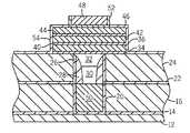
- FIG. 1is an enlarged, cross-sectional view of one embodiment of the present invention.
- erosion of chalcogenide during the etching of overlying stacksmay be reduced through appropriate design of overlying electrode layers.
- electrodes used in connection with overlying ovonic threshold switchesmay be prone to the formation of cracks. It is believed, without being limited by theory, that these cracks are the result of columnar morphology of metal nitride electrodes.
- the columnar structures in metal nitride electrode filmmay be grains or grain-like nanostructures.
- the cracksmay be formed at grain or grain-like nanostructure boundaries.
- the grain-like nanostructuresmay be crystallites, for example.
- the columnar morphologyresults in vertical cracks which may allow etchant materials to sneak through these cracks and to etch out underlying chalcogenide material which may be highly susceptible to the etchants used to etch overlying stacks of materials.
- Undesired erosion of chalcogenidesmay be reduced by reducing the thickness of the overlying metal nitride electrodes. Reducing their thickness reduces their tendency to form columnar morphology.
- the electrodemay be split into two separate sub-layers, for example, separated by an intervening layer of a different material. The layer of a different material may also interfere with the formation of columnar morphology. In addition, even if the constituent sub-layers form cracks, it is unlikely that the cracks would line up sufficiently to allow etchant penetration through both sub-layers.
- the columnar morphologymay be disrupted and, if not, the formation of cracks completely through both sub-layers is unlikely.
- a metal nitridewhen used for the electrode, that same metal may be used as the intervening layer, providing the desired disruption of the columnar morphology or penetrating cracks and good adherence to the nitride in some embodiments.
- a phase change memory cellmay include a phase change memory element in series with an overlying ovonic threshold switch that functions as a select device.
- a phase change memorymay include an array of cells coupled by row lines and bitlines.
- a first address line 12 at the bottommay extend from left to right.
- a second address line 48 at the topmay extend into the page perpendicularly to the first address line 12 .
- One address linemay be a row line and the other address line may be a perpendicularly oriented bitline.
- a heater 50which, in one embodiment, may be titanium silicon nitride.
- the heater 50may be isolated using tantalum nitride barrier layer 20 .
- the heater 50may be encased within a pore formed of two layers of distinct dielectrics 14 and 16 .
- the layer 14may be nitride and the layer 16 may be oxide.
- another pore above the heatermay be filled with additional heater material 30 and a chalcogenide material 32 .
- That poremay be defined by two different dielectric layers 22 and 24 .
- the lower dielectric layer 22may be nitride and the upper dielectric layer 24 may be oxide.
- sidewall spacersmay reduce the size of the pore.
- an outer sidewall spacer 26may enclose an inner sidewall spacer 28 .
- the outer sidewall spacer 26may, for example, be oxide and the inner sidewall spacer 28 may, for example, be nitride.
- the ovonic threshold switchmay include a first electrode 34 which, in one embodiment, may be titanium aluminum nitride.
- the next layer 36may include a chalcogenide that forms the ovonic threshold switch.
- Thisis followed by a layer 40 which, in one embodiment, may be carbon.
- a layer 42may be an electrode layer formed of a metal nitride, such as titanium nitride.
- a second electrode layer 46may be formed above the first electrode layer 42 , separated by an intervening conductor 44 .
- the electrode layers 42 and 46may be formed of a conductive material other than a metal nitride, including a metal without nitride.
- the conductor 44may be formed of the same metal used to form the metal nitride of the layers 42 and 46 in some embodiments. Generally, the layers 42 and 46 may be of the same material, but this is not necessarily so.
- the intervening conductor 44may serve, in some embodiments, to break up the columnar structure of the metal nitride layers 42 and 46 by disrupting columns that would otherwise form across the layers 42 and 46 and by enabling reduced thicknesses of those layers.
- the upper layer 46may be masked and the entire stack etched using suitable etchants. As a result, the edges of the layers 34 , 36 , 40 , 42 , 44 , and 46 are aligned.
- the stack of aligned layersmay be covered by a sealing layer 54 in some embodiments.
- the erosion of chalcogenide in the layers 32 and/or 36 , through cracks formed due to the columnar morphology,may be reduced by reducing the thickness of the layers 42 and 46 by breaking them into two layers and by providing the intervening conductor 44 that is of a different material than the material used for the layers 42 and 46 , in some embodiments.
- the thicknesses of the layers 42 and 46may be less than 350 Angstroms.
- the intervening conductor 44may be from 20 to 100 Angstroms thick in some embodiments. In one embodiment, the conductor 44 is about 50 Angstroms thick. It is desirable that the intervening layer be relatively thin, in some embodiments, to reduce the formation of columnar morphology in that layer as well.
- the upper address line 48may be isolated using a tantalum nitride layer 52 , particularly when the upper address line 48 is formed of a copper material. Copper may migrate down through the chalcogenides 32 and/or 36 causing damage. Damage from the lower address line 12 may be reduced in cases where the lower address line 12 is copper by encasing the heater 50 in a tantalum nitride or other barrier layer 20 .
- the columnar morphology referred to hereinmay loosely be the result of columnar shaped grains that may be formed within the metal nitride structure. These columnar grains may be vertically oriented, providing vertical paths down through the metal nitride. These paths may be referred to as cracks. As a result, etchants may penetrate through these cracks and travel downwardly all the way down to the chalcogenide. The chalcogenide may be eroded during the etching of the overlying stack used to form the ovonic threshold switch.
- More than two metal nitride layers with more than one 25 separating metal layermay be used in some embodiments.
- Using the same metal for the layer 44 as is used for the layers 42 and 46may be advantageous in some cases. It enables all three layers to be formed in the same deposition chamber. It allows the same targets to be used in some cases. And, in some cases, the conductor 44 may adhere better to its own metal nitrides than would other metals. However, different metals may be used in the layers 42 , 44 , and 46 in some embodiments.
- Programming to alter the state or phase of the materialmay be accomplished by applying voltage potentials to the address lines 12 and 48 , thereby generating a voltage potential across a memory element including a phase change material 32 .
- the voltage potentialis greater than the threshold voltages of any select device and memory element, then an electrical current may flow through the phase change material 32 in response to the applied voltage potentials, and may result in heating of the phase change material 32 .
- This heatingmay alter the memory state or phase of the material 32 , in one embodiment. Altering the phase or state of the material 32 may alter the electrical characteristic of memory material, e.g., the resistance or threshold voltage of the material may be altered by altering the phase of the memory material. Memory material may also be referred to as a programmable resistance material.
- memory materialIn the “reset” state, memory material may be in an amorphous or semi-amorphous state and in the “set” state, memory material may be in a crystalline or semi-crystalline state.
- the resistance of memory material in the amorphous or semi-amorphous statemay be greater than the resistance of memory material in the crystalline or semi-crystalline state.
- memory materialmay be heated to a relatively higher temperature to melt and then quenched to vitrify and “reset” memory material in an amorphous state (e.g., program memory material to a logic 15 “0” value). Heating the volume of memory material to a relatively lower crystallization temperature may crystallize or devitrify memory material and “set” memory material (e.g., program memory material to a logic “1” value).
- Various resistances of memory materialmay be achieved to store information by varying the amount of current flow and duration through the volume of memory material.
- the ovonic threshold switchis either on or off depending on the amount of voltage potential applied across the switch and, more particularly, whether the current through the switch exceeds its threshold current or voltage, which then triggers the device into an on state.
- the off statemay be substantially electrically nonconductive and the on state may be a substantially conductive state with less resistance than the off state.
- the voltage across the switchin one embodiment, is equal to its holding voltage V hold ‘R on /where R on is the dynamic resistance from the extrapolated X axis intercept V hold .
- an ovonic threshold switchmay have a threshold voltage V th and, if a voltage potential less than the threshold voltage of the switch is applied across the switch, then the switch may remain off or in a relatively high resistance state so that little or no electrical current passes.
- each switchmay comprise a switch material 36 that is a chalcogenide alloy.
- the switch materialmay be a material in a substantial amorphous state positioned between two electrodes that may be repeatedly and reversibly switched between a higher resistance off state that is generally greater than about 1 megaOhms and a relatively lower resistance on state that is generally less than about 1000 Ohms in series with the holding voltage by the application of electrical current or potential.
- Each switchis a two-terminal device that has an IV curve similar to that of a phase change memory element that is in an amorphous state.
- the ovonic threshold switchdoes not change phase. That is, the switching material of the ovonic threshold switch is not a phase programmable material and, as a result, the switch may not be a memory device capable of storing information. For example, the switching material may remain permanently amorphous and the IV characteristics may remain the same throughout the operating life.
- the switchIn the low voltage, low electric field mode, where the voltage applied across the switch is less than the threshold voltage V th ; the switch may be off or non-conducting and exhibits a relatively high resistance.
- the switchmay remain in the off state until a sufficient voltage, namely, the threshold voltage, is applied or a sufficient current is applied, namely, the threshold current, that switches the device to a conductive relatively low resistance on state.
- a sufficient voltagenamely, the threshold voltage
- a sufficient currentnamely, the threshold current
- the voltage potential across the devicemay drop or snapback to a holding voltage V hold . Snapback may refer to the voltage difference between the threshold voltage and the holding voltage of the switch.
- the voltage potential across the switchmay remain close to the holding voltage as current passing through the switch is increased.
- the switchmay remain on until the current through the switch drops below a holding current. Below this value, the switch may turn off and return to a relatively high resistance, non-conductive off state, until the threshold voltage and current are again exceeded.
- only one switchmay be used. In other embodiments, two or more series connected switches may be used.
- references throughout this specification to “one embodiment” or “an embodiment”mean that a particular feature, structure, or characteristic described in connection with the embodiment is included in at least one implementation encompassed within the present invention. Thus, appearances of the phrase “one embodiment” or “in an embodiment” are not necessarily referring to the same embodiment. Furthermore, the particular features, structures, or characteristics may be instituted in other suitable forms other than the particular embodiment illustrated and all such forms may be encompassed within the claims of the present application.
Landscapes
- Engineering & Computer Science (AREA)
- Manufacturing & Machinery (AREA)
- Semiconductor Memories (AREA)
Abstract
Description
Claims (24)
Priority Applications (1)
| Application Number | Priority Date | Filing Date | Title |
|---|---|---|---|
| US14/013,361US9029826B2 (en) | 2010-05-06 | 2013-08-29 | Phase change memory including ovonic threshold switch with layered electrode and methods for forming the same |
Applications Claiming Priority (2)
| Application Number | Priority Date | Filing Date | Title |
|---|---|---|---|
| US12/774,772US8530875B1 (en) | 2010-05-06 | 2010-05-06 | Phase change memory including ovonic threshold switch with layered electrode and methods for forming same |
| US14/013,361US9029826B2 (en) | 2010-05-06 | 2013-08-29 | Phase change memory including ovonic threshold switch with layered electrode and methods for forming the same |
Related Parent Applications (1)
| Application Number | Title | Priority Date | Filing Date |
|---|---|---|---|
| US12/774,772ContinuationUS8530875B1 (en) | 2010-05-06 | 2010-05-06 | Phase change memory including ovonic threshold switch with layered electrode and methods for forming same |
Publications (2)
| Publication Number | Publication Date |
|---|---|
| US20130344676A1 US20130344676A1 (en) | 2013-12-26 |
| US9029826B2true US9029826B2 (en) | 2015-05-12 |
Family
ID=49084107
Family Applications (2)
| Application Number | Title | Priority Date | Filing Date |
|---|---|---|---|
| US12/774,772Active2030-10-09US8530875B1 (en) | 2010-05-06 | 2010-05-06 | Phase change memory including ovonic threshold switch with layered electrode and methods for forming same |
| US14/013,361ActiveUS9029826B2 (en) | 2010-05-06 | 2013-08-29 | Phase change memory including ovonic threshold switch with layered electrode and methods for forming the same |
Family Applications Before (1)
| Application Number | Title | Priority Date | Filing Date |
|---|---|---|---|
| US12/774,772Active2030-10-09US8530875B1 (en) | 2010-05-06 | 2010-05-06 | Phase change memory including ovonic threshold switch with layered electrode and methods for forming same |
Country Status (1)
| Country | Link |
|---|---|
| US (2) | US8530875B1 (en) |
Cited By (5)
| Publication number | Priority date | Publication date | Assignee | Title |
|---|---|---|---|---|
| US9780144B2 (en) | 2016-02-22 | 2017-10-03 | Samsung Electronics Co., Ltd. | Memory device and method of manufacturing the same |
| US10062844B2 (en) | 2013-02-25 | 2018-08-28 | Micron Technology, Inc. | Apparatuses including electrodes having a conductive barrier material and methods of forming same |
| US10424619B2 (en) | 2016-01-13 | 2019-09-24 | Samsung Electronics Co., Ltd. | Variable resistance memory devices and methods of manufacturing the same |
| US20210280533A1 (en)* | 2018-07-30 | 2021-09-09 | Texas Instruments Incorporated | Crack suppression structure for hv isolation component |
| US11387410B2 (en) | 2019-06-07 | 2022-07-12 | Samsung Electronics Co., Ltd. | Semiconductor device including data storage material pattern |
Families Citing this family (12)
| Publication number | Priority date | Publication date | Assignee | Title |
|---|---|---|---|---|
| EP1677371A1 (en) | 2004-12-30 | 2006-07-05 | STMicroelectronics S.r.l. | Dual resistance heater for phase change devices and manufacturing method thereof |
| US9595669B2 (en) | 2015-06-30 | 2017-03-14 | Western Digital Technologies, Inc. | Electroplated phase change switch |
| US9564585B1 (en) | 2015-09-03 | 2017-02-07 | HGST Netherlands B.V. | Multi-level phase change device |
| KR102375591B1 (en) | 2015-10-27 | 2022-03-16 | 삼성전자주식회사 | Semiconductor device and method for fabricating the same |
| US10490742B2 (en) | 2017-08-28 | 2019-11-26 | Taiwan Seminconductor Manufacturing Co., Ltd. | Method for forming a phase change memory (PCM) cell with a low deviation contact area between a heater and a phase change element |
| KR20200126971A (en) | 2018-03-02 | 2020-11-09 | 소니 세미컨덕터 솔루션즈 가부시키가이샤 | Switch elements and storage devices, and memory systems |
| US10622555B2 (en) | 2018-07-31 | 2020-04-14 | Taiwan Semiconductor Manufacturing Co., Ltd. | Film scheme to improve peeling in chalcogenide based PCRAM |
| KR102549544B1 (en)* | 2018-09-03 | 2023-06-29 | 삼성전자주식회사 | Memory devices |
| US10971684B2 (en)* | 2018-10-30 | 2021-04-06 | Taiwan Semiconductor Manufacturing Co., Ltd. | Intercalated metal/dielectric structure for nonvolatile memory devices |
| US11139430B2 (en) | 2018-10-31 | 2021-10-05 | Taiwan Semiconductor Manufacturing Co., Ltd. | Phase change random access memory and method of manufacturing |
| KR102702790B1 (en) | 2019-07-12 | 2024-09-05 | 에스케이하이닉스 주식회사 | Electronic device and method for fabricating electronic device |
| US11271036B2 (en) | 2020-06-24 | 2022-03-08 | Sandisk Technologies Llc | Memory device containing dual etch stop layers for selector elements and method of making the same |
Citations (37)
| Publication number | Priority date | Publication date | Assignee | Title |
|---|---|---|---|---|
| US4845533A (en) | 1986-08-22 | 1989-07-04 | Energy Conversion Devices, Inc. | Thin film electrical devices with amorphous carbon electrodes and method of making same |
| US5414271A (en)* | 1991-01-18 | 1995-05-09 | Energy Conversion Devices, Inc. | Electrically erasable memory elements having improved set resistance stability |
| US5714768A (en)* | 1995-10-24 | 1998-02-03 | Energy Conversion Devices, Inc. | Second-layer phase change memory array on top of a logic device |
| US5920122A (en) | 1994-08-18 | 1999-07-06 | Oki Electric Industry Co., Ltd. | Contact structure using barrier metal and method of manufacturing the same |
| US20040037179A1 (en) | 2002-08-23 | 2004-02-26 | Se-Ho Lee | Phase-changeable devices having an insulating buffer layer and methods of fabricating the same |
| US20050023581A1 (en) | 2003-07-29 | 2005-02-03 | International Business Machines Corporation | Magnetic random access memory and method of fabricating thereof |
| US20060091492A1 (en)* | 2004-10-28 | 2006-05-04 | Jong-Won Lee | Depositing titanium silicon nitride films for forming phase change memories |
| US20060237756A1 (en) | 2005-04-20 | 2006-10-26 | Jae-Hyun Park | Phase change memory devices and their methods of fabrication |
| US20060246712A1 (en) | 2004-12-30 | 2006-11-02 | Stmicroelectronics S.R.I. | Dual resistance heater for phase change devices and manufacturing method thereof |
| US20060255328A1 (en) | 2005-05-12 | 2006-11-16 | Dennison Charles H | Using conductive oxidation for phase change memory electrodes |
| US20070096090A1 (en)* | 2005-10-28 | 2007-05-03 | Dennison Charles H | Forming a phase change memory with an ovonic threshold switch |
| US20070158698A1 (en)* | 2005-12-23 | 2007-07-12 | Stmicroelectronics S.R.L. | Process for manufacturing a phase change selection device with reduced current leakage, and phase change selection device, in particular for phase change memory devices |
| US20070210296A1 (en) | 2006-03-07 | 2007-09-13 | International Business Machines Corporation | Electrode for phase change memory device and method |
| US20080020508A1 (en)* | 2005-06-28 | 2008-01-24 | Dennison Charles H | Reducing oxidation of phase change memory electrodes |
| US7332735B2 (en) | 2005-08-02 | 2008-02-19 | Micron Technology, Inc. | Phase change memory cell and method of formation |
| US20080067486A1 (en)* | 2005-09-14 | 2008-03-20 | Stmicroelectronics S.R.L. | Ring heater for a phase change memory device |
| US20080102560A1 (en) | 2006-10-10 | 2008-05-01 | Stmicroelectronics S.R.L. | Method of forming phase change memory devices in a pulsed DC deposition chamber |
| US20080121862A1 (en) | 2006-08-30 | 2008-05-29 | Micron Technology, Inc. | Bottom electrode geometry for phase change memory |
| US20080137262A1 (en) | 2006-12-12 | 2008-06-12 | Texas Instruments Inc. | Methods and systems for capacitors |
| US20080142984A1 (en) | 2006-12-15 | 2008-06-19 | Macronix International Co., Ltd. | Multi-Layer Electrode Structure |
| US20090014705A1 (en) | 2007-07-09 | 2009-01-15 | Industrial Technology Research Institute | Phase change memory device and method for fabricating the same |
| US20090050872A1 (en)* | 2007-07-17 | 2009-02-26 | Stmicroelectronics S.R.L. | Process for manufacturing a copper compatible chalcogenide phase change memory element and corresponding phase change memory element |
| US20090122588A1 (en) | 2007-11-14 | 2009-05-14 | Macronix International Co., Ltd. | Phase change memory cell including a thermal protect bottom electrode and manufacturing methods |
| US20090194758A1 (en) | 2008-02-05 | 2009-08-06 | Macronix International Co., Ltd. | Heating center pcram structure and methods for making |
| US20090218557A1 (en)* | 2008-03-03 | 2009-09-03 | Elpida Memory, Inc. | Phase change memory device and fabrication method thereof |
| US20090246952A1 (en) | 2008-03-28 | 2009-10-01 | Tokyo Electron Limited | Method of forming a cobalt metal nitride barrier film |
| US20090298222A1 (en)* | 2008-05-28 | 2009-12-03 | Ovonyx, Inc. | Method for manufacturing Chalcogenide devices |
| US20090298224A1 (en)* | 2002-12-13 | 2009-12-03 | Lowrey Tyler A | Memory and Access Device and Method Therefor |
| US20100032638A1 (en) | 2008-08-07 | 2010-02-11 | Sandisk 3D Llc | Memory cell that includes a carbon-based memory element and methods of forming the same |
| US20100163818A1 (en)* | 2008-12-30 | 2010-07-01 | Stmicroelectronics S.R.L. | Forming a carbon passivated ovonic threshold switch |
| US20110007545A1 (en) | 2009-07-13 | 2011-01-13 | Seagate Technology Llc | Non-Volatile Memory Cell Stack with Dual Resistive Elements |
| US20110147695A1 (en) | 2009-12-23 | 2011-06-23 | Jong-Won Sean Lee | Fabricating current-confining structures in phase change memory switch cells |
| US8237146B2 (en) | 2010-02-24 | 2012-08-07 | Sandisk 3D Llc | Memory cell with silicon-containing carbon switching layer and methods for forming the same |
| US20120224413A1 (en) | 2011-03-02 | 2012-09-06 | Jingyan Zhang | Non-Volatile Storage System Using Opposite Polarity Programming Signals For MIM Memory Cell |
| US8263455B2 (en) | 2009-11-25 | 2012-09-11 | Samsung Electronics Co., Ltd. | Method of forming variable resistance memory device |
| WO2013039496A1 (en) | 2011-09-14 | 2013-03-21 | Intel Corporation | Electrodes for resistance change memory devices |
| US20140239245A1 (en) | 2013-02-25 | 2014-08-28 | Micron Technology, Inc. | Apparatuses including electrodes having a conductive barrier material and methods of forming same |
- 2010
- 2010-05-06USUS12/774,772patent/US8530875B1/enactiveActive
- 2013
- 2013-08-29USUS14/013,361patent/US9029826B2/enactiveActive
Patent Citations (38)
| Publication number | Priority date | Publication date | Assignee | Title |
|---|---|---|---|---|
| US4845533A (en) | 1986-08-22 | 1989-07-04 | Energy Conversion Devices, Inc. | Thin film electrical devices with amorphous carbon electrodes and method of making same |
| US5414271A (en)* | 1991-01-18 | 1995-05-09 | Energy Conversion Devices, Inc. | Electrically erasable memory elements having improved set resistance stability |
| US5920122A (en) | 1994-08-18 | 1999-07-06 | Oki Electric Industry Co., Ltd. | Contact structure using barrier metal and method of manufacturing the same |
| US5714768A (en)* | 1995-10-24 | 1998-02-03 | Energy Conversion Devices, Inc. | Second-layer phase change memory array on top of a logic device |
| US20040037179A1 (en) | 2002-08-23 | 2004-02-26 | Se-Ho Lee | Phase-changeable devices having an insulating buffer layer and methods of fabricating the same |
| US20090298224A1 (en)* | 2002-12-13 | 2009-12-03 | Lowrey Tyler A | Memory and Access Device and Method Therefor |
| US20050023581A1 (en) | 2003-07-29 | 2005-02-03 | International Business Machines Corporation | Magnetic random access memory and method of fabricating thereof |
| US20060091492A1 (en)* | 2004-10-28 | 2006-05-04 | Jong-Won Lee | Depositing titanium silicon nitride films for forming phase change memories |
| US20060246712A1 (en) | 2004-12-30 | 2006-11-02 | Stmicroelectronics S.R.I. | Dual resistance heater for phase change devices and manufacturing method thereof |
| US20060237756A1 (en) | 2005-04-20 | 2006-10-26 | Jae-Hyun Park | Phase change memory devices and their methods of fabrication |
| US20060255328A1 (en) | 2005-05-12 | 2006-11-16 | Dennison Charles H | Using conductive oxidation for phase change memory electrodes |
| US20080020508A1 (en)* | 2005-06-28 | 2008-01-24 | Dennison Charles H | Reducing oxidation of phase change memory electrodes |
| US7332735B2 (en) | 2005-08-02 | 2008-02-19 | Micron Technology, Inc. | Phase change memory cell and method of formation |
| US20080067486A1 (en)* | 2005-09-14 | 2008-03-20 | Stmicroelectronics S.R.L. | Ring heater for a phase change memory device |
| US20070096090A1 (en)* | 2005-10-28 | 2007-05-03 | Dennison Charles H | Forming a phase change memory with an ovonic threshold switch |
| US20070158698A1 (en)* | 2005-12-23 | 2007-07-12 | Stmicroelectronics S.R.L. | Process for manufacturing a phase change selection device with reduced current leakage, and phase change selection device, in particular for phase change memory devices |
| US20070210296A1 (en) | 2006-03-07 | 2007-09-13 | International Business Machines Corporation | Electrode for phase change memory device and method |
| US20080121862A1 (en) | 2006-08-30 | 2008-05-29 | Micron Technology, Inc. | Bottom electrode geometry for phase change memory |
| US20080102560A1 (en) | 2006-10-10 | 2008-05-01 | Stmicroelectronics S.R.L. | Method of forming phase change memory devices in a pulsed DC deposition chamber |
| US20080137262A1 (en) | 2006-12-12 | 2008-06-12 | Texas Instruments Inc. | Methods and systems for capacitors |
| US20080142984A1 (en) | 2006-12-15 | 2008-06-19 | Macronix International Co., Ltd. | Multi-Layer Electrode Structure |
| US20090014705A1 (en) | 2007-07-09 | 2009-01-15 | Industrial Technology Research Institute | Phase change memory device and method for fabricating the same |
| US20090050872A1 (en)* | 2007-07-17 | 2009-02-26 | Stmicroelectronics S.R.L. | Process for manufacturing a copper compatible chalcogenide phase change memory element and corresponding phase change memory element |
| US20090122588A1 (en) | 2007-11-14 | 2009-05-14 | Macronix International Co., Ltd. | Phase change memory cell including a thermal protect bottom electrode and manufacturing methods |
| US7804083B2 (en) | 2007-11-14 | 2010-09-28 | Macronix International Co., Ltd. | Phase change memory cell including a thermal protect bottom electrode and manufacturing methods |
| US20090194758A1 (en) | 2008-02-05 | 2009-08-06 | Macronix International Co., Ltd. | Heating center pcram structure and methods for making |
| US20090218557A1 (en)* | 2008-03-03 | 2009-09-03 | Elpida Memory, Inc. | Phase change memory device and fabrication method thereof |
| US20090246952A1 (en) | 2008-03-28 | 2009-10-01 | Tokyo Electron Limited | Method of forming a cobalt metal nitride barrier film |
| US20090298222A1 (en)* | 2008-05-28 | 2009-12-03 | Ovonyx, Inc. | Method for manufacturing Chalcogenide devices |
| US20100032638A1 (en) | 2008-08-07 | 2010-02-11 | Sandisk 3D Llc | Memory cell that includes a carbon-based memory element and methods of forming the same |
| US20100163818A1 (en)* | 2008-12-30 | 2010-07-01 | Stmicroelectronics S.R.L. | Forming a carbon passivated ovonic threshold switch |
| US20110007545A1 (en) | 2009-07-13 | 2011-01-13 | Seagate Technology Llc | Non-Volatile Memory Cell Stack with Dual Resistive Elements |
| US8263455B2 (en) | 2009-11-25 | 2012-09-11 | Samsung Electronics Co., Ltd. | Method of forming variable resistance memory device |
| US20110147695A1 (en) | 2009-12-23 | 2011-06-23 | Jong-Won Sean Lee | Fabricating current-confining structures in phase change memory switch cells |
| US8237146B2 (en) | 2010-02-24 | 2012-08-07 | Sandisk 3D Llc | Memory cell with silicon-containing carbon switching layer and methods for forming the same |
| US20120224413A1 (en) | 2011-03-02 | 2012-09-06 | Jingyan Zhang | Non-Volatile Storage System Using Opposite Polarity Programming Signals For MIM Memory Cell |
| WO2013039496A1 (en) | 2011-09-14 | 2013-03-21 | Intel Corporation | Electrodes for resistance change memory devices |
| US20140239245A1 (en) | 2013-02-25 | 2014-08-28 | Micron Technology, Inc. | Apparatuses including electrodes having a conductive barrier material and methods of forming same |
Non-Patent Citations (2)
| Title |
|---|
| International Search Report for PCT Application No. PCT/US2011/051600 dated May 1, 2012. |
| Park et al., "Comparison of TiN and TiN/Ti/TiN Multilayer Films for Diffusion Barrier Applications", Journal of the Korean Physical Society, vol. 42, No. 6, Jun. 2003, pp. 817-820.* |
Cited By (13)
| Publication number | Priority date | Publication date | Assignee | Title |
|---|---|---|---|---|
| US10950791B2 (en) | 2013-02-25 | 2021-03-16 | Micron Technology, Inc. | Apparatuses including electrodes having a conductive barrier material and methods of forming same |
| US10062844B2 (en) | 2013-02-25 | 2018-08-28 | Micron Technology, Inc. | Apparatuses including electrodes having a conductive barrier material and methods of forming same |
| US10069069B2 (en) | 2013-02-25 | 2018-09-04 | Micron Technology, Inc. | Apparatuses including electrodes having a conductive barrier material and methods of forming same |
| US10217936B2 (en) | 2013-02-25 | 2019-02-26 | Micron Technology, Inc. | Apparatuses including electrodes having a conductive barrier material and methods of forming same |
| US10651381B2 (en) | 2013-02-25 | 2020-05-12 | Micron Technology, Inc. | Apparatuses including electrodes having a conductive barrier material and methods of forming same |
| US10957855B2 (en) | 2013-02-25 | 2021-03-23 | Micron Technology, Inc. | Apparatuses including electrodes having a conductive barrier material and methods of forming same |
| US11081644B2 (en) | 2013-02-25 | 2021-08-03 | Micron Technology, Inc. | Apparatuses including electrodes having a conductive barrier material and methods of forming same |
| US10424619B2 (en) | 2016-01-13 | 2019-09-24 | Samsung Electronics Co., Ltd. | Variable resistance memory devices and methods of manufacturing the same |
| US9780144B2 (en) | 2016-02-22 | 2017-10-03 | Samsung Electronics Co., Ltd. | Memory device and method of manufacturing the same |
| US11587977B2 (en) | 2016-02-22 | 2023-02-21 | Samsung Electronics Co., Ltd. | Memory device and method of manufacturing the same |
| US11770938B2 (en) | 2016-02-22 | 2023-09-26 | Samsung Electronics Co., Ltd. | Memory device and method of manufacturing the same |
| US20210280533A1 (en)* | 2018-07-30 | 2021-09-09 | Texas Instruments Incorporated | Crack suppression structure for hv isolation component |
| US11387410B2 (en) | 2019-06-07 | 2022-07-12 | Samsung Electronics Co., Ltd. | Semiconductor device including data storage material pattern |
Also Published As
| Publication number | Publication date |
|---|---|
| US8530875B1 (en) | 2013-09-10 |
| US20130344676A1 (en) | 2013-12-26 |
Similar Documents
| Publication | Publication Date | Title |
|---|---|---|
| US9029826B2 (en) | Phase change memory including ovonic threshold switch with layered electrode and methods for forming the same | |
| US7220983B2 (en) | Self-aligned small contact phase-change memory method and device | |
| US9159915B2 (en) | Phase change memory with threshold switch select device | |
| US7449710B2 (en) | Vacuum jacket for phase change memory element | |
| US8440535B2 (en) | Forming a phase change memory with an ovonic threshold switch | |
| CN100544051C (en) | Method for forming self-aligned thermal isolation cells in a variable resistance memory array | |
| EP1801896B1 (en) | Process for manufacturing a selection device with reduced current leakage, and selection device, in particular for phase change memory devices | |
| US8030734B2 (en) | Forming phase change memories with a breakdown layer sandwiched by phase change memory material | |
| US9705080B2 (en) | Forming self-aligned conductive lines for resistive random access memories | |
| US20070200108A1 (en) | Storage node, phase change random access memory and methods of fabricating the same | |
| EP1677372B1 (en) | Phase change memory and manufacturing method thereof | |
| KR102277861B1 (en) | Memory cell with resistance and its formation | |
| US8995171B2 (en) | Designing method of non-volatile memory device, manufacturing method of non-volatile memory device, and non-volatile memory device | |
| US20230047263A1 (en) | Elementary cell comprising a resistive memory and a device intended to form a selector, cell matrix, associated manufacturing and initialization methods | |
| US7105408B2 (en) | Phase change memory with a select device having a breakdown layer | |
| US10109681B2 (en) | Vertical memory structure with array interconnects and method for producing the same | |
| US11711988B2 (en) | Elementary cell comprising a resistive memory and associated method of initialization | |
| US7755074B2 (en) | Low area contact phase-change memory | |
| US20130284998A1 (en) | Forming heaters for phase change memories | |
| US20230171967A1 (en) | Semiconductor device and method for fabricating the same | |
| CN118234250A (en) | Semiconductor devices | |
| US20250081471A1 (en) | Semiconductor device and method of manufacturing semiconductor device | |
| CN105185902B (en) | A kind of resistor-type memory cell |
Legal Events
| Date | Code | Title | Description |
|---|---|---|---|
| FEPP | Fee payment procedure | Free format text:PAYOR NUMBER ASSIGNED (ORIGINAL EVENT CODE: ASPN); ENTITY STATUS OF PATENT OWNER: LARGE ENTITY | |
| STCF | Information on status: patent grant | Free format text:PATENTED CASE | |
| AS | Assignment | Owner name:U.S. BANK NATIONAL ASSOCIATION, AS COLLATERAL AGENT, CALIFORNIA Free format text:SECURITY INTEREST;ASSIGNOR:MICRON TECHNOLOGY, INC.;REEL/FRAME:038669/0001 Effective date:20160426 Owner name:U.S. BANK NATIONAL ASSOCIATION, AS COLLATERAL AGEN Free format text:SECURITY INTEREST;ASSIGNOR:MICRON TECHNOLOGY, INC.;REEL/FRAME:038669/0001 Effective date:20160426 | |
| AS | Assignment | Owner name:MORGAN STANLEY SENIOR FUNDING, INC., AS COLLATERAL AGENT, MARYLAND Free format text:PATENT SECURITY AGREEMENT;ASSIGNOR:MICRON TECHNOLOGY, INC.;REEL/FRAME:038954/0001 Effective date:20160426 Owner name:MORGAN STANLEY SENIOR FUNDING, INC., AS COLLATERAL Free format text:PATENT SECURITY AGREEMENT;ASSIGNOR:MICRON TECHNOLOGY, INC.;REEL/FRAME:038954/0001 Effective date:20160426 | |
| AS | Assignment | Owner name:U.S. BANK NATIONAL ASSOCIATION, AS COLLATERAL AGENT, CALIFORNIA Free format text:CORRECTIVE ASSIGNMENT TO CORRECT THE REPLACE ERRONEOUSLY FILED PATENT #7358718 WITH THE CORRECT PATENT #7358178 PREVIOUSLY RECORDED ON REEL 038669 FRAME 0001. ASSIGNOR(S) HEREBY CONFIRMS THE SECURITY INTEREST;ASSIGNOR:MICRON TECHNOLOGY, INC.;REEL/FRAME:043079/0001 Effective date:20160426 Owner name:U.S. BANK NATIONAL ASSOCIATION, AS COLLATERAL AGEN Free format text:CORRECTIVE ASSIGNMENT TO CORRECT THE REPLACE ERRONEOUSLY FILED PATENT #7358718 WITH THE CORRECT PATENT #7358178 PREVIOUSLY RECORDED ON REEL 038669 FRAME 0001. ASSIGNOR(S) HEREBY CONFIRMS THE SECURITY INTEREST;ASSIGNOR:MICRON TECHNOLOGY, INC.;REEL/FRAME:043079/0001 Effective date:20160426 | |
| AS | Assignment | Owner name:JPMORGAN CHASE BANK, N.A., AS COLLATERAL AGENT, ILLINOIS Free format text:SECURITY INTEREST;ASSIGNORS:MICRON TECHNOLOGY, INC.;MICRON SEMICONDUCTOR PRODUCTS, INC.;REEL/FRAME:047540/0001 Effective date:20180703 Owner name:JPMORGAN CHASE BANK, N.A., AS COLLATERAL AGENT, IL Free format text:SECURITY INTEREST;ASSIGNORS:MICRON TECHNOLOGY, INC.;MICRON SEMICONDUCTOR PRODUCTS, INC.;REEL/FRAME:047540/0001 Effective date:20180703 | |
| AS | Assignment | Owner name:MICRON TECHNOLOGY, INC., IDAHO Free format text:RELEASE BY SECURED PARTY;ASSIGNOR:U.S. BANK NATIONAL ASSOCIATION, AS COLLATERAL AGENT;REEL/FRAME:047243/0001 Effective date:20180629 | |
| MAFP | Maintenance fee payment | Free format text:PAYMENT OF MAINTENANCE FEE, 4TH YEAR, LARGE ENTITY (ORIGINAL EVENT CODE: M1551); ENTITY STATUS OF PATENT OWNER: LARGE ENTITY Year of fee payment:4 | |
| AS | Assignment | Owner name:MICRON TECHNOLOGY, INC., IDAHO Free format text:RELEASE BY SECURED PARTY;ASSIGNOR:MORGAN STANLEY SENIOR FUNDING, INC., AS COLLATERAL AGENT;REEL/FRAME:050937/0001 Effective date:20190731 | |
| AS | Assignment | Owner name:MICRON SEMICONDUCTOR PRODUCTS, INC., IDAHO Free format text:RELEASE BY SECURED PARTY;ASSIGNOR:JPMORGAN CHASE BANK, N.A., AS COLLATERAL AGENT;REEL/FRAME:051028/0001 Effective date:20190731 Owner name:MICRON TECHNOLOGY, INC., IDAHO Free format text:RELEASE BY SECURED PARTY;ASSIGNOR:JPMORGAN CHASE BANK, N.A., AS COLLATERAL AGENT;REEL/FRAME:051028/0001 Effective date:20190731 | |
| MAFP | Maintenance fee payment | Free format text:PAYMENT OF MAINTENANCE FEE, 8TH YEAR, LARGE ENTITY (ORIGINAL EVENT CODE: M1552); ENTITY STATUS OF PATENT OWNER: LARGE ENTITY Year of fee payment:8 |