US9025305B2 - High surface resistivity electrostatic chuck - Google Patents
High surface resistivity electrostatic chuckDownload PDFInfo
- Publication number
- US9025305B2 US9025305B2US13/699,279US201113699279AUS9025305B2US 9025305 B2US9025305 B2US 9025305B2US 201113699279 AUS201113699279 AUS 201113699279AUS 9025305 B2US9025305 B2US 9025305B2
- Authority
- US
- United States
- Prior art keywords
- electrostatic chuck
- charge control
- control layer
- surface resistivity
- layer
- Prior art date
- Legal status (The legal status is an assumption and is not a legal conclusion. Google has not performed a legal analysis and makes no representation as to the accuracy of the status listed.)
- Active
Links
Images


Classifications
- B—PERFORMING OPERATIONS; TRANSPORTING
- B23—MACHINE TOOLS; METAL-WORKING NOT OTHERWISE PROVIDED FOR
- B23Q—DETAILS, COMPONENTS, OR ACCESSORIES FOR MACHINE TOOLS, e.g. ARRANGEMENTS FOR COPYING OR CONTROLLING; MACHINE TOOLS IN GENERAL CHARACTERISED BY THE CONSTRUCTION OF PARTICULAR DETAILS OR COMPONENTS; COMBINATIONS OR ASSOCIATIONS OF METAL-WORKING MACHINES, NOT DIRECTED TO A PARTICULAR RESULT
- B23Q3/00—Devices holding, supporting, or positioning work or tools, of a kind normally removable from the machine
- B23Q3/15—Devices for holding work using magnetic or electric force acting directly on the work
- B23Q3/152—Rotary devices
- H—ELECTRICITY
- H02—GENERATION; CONVERSION OR DISTRIBUTION OF ELECTRIC POWER
- H02N—ELECTRIC MACHINES NOT OTHERWISE PROVIDED FOR
- H02N13/00—Clutches or holding devices using electrostatic attraction, e.g. using Johnson-Rahbek effect
- B—PERFORMING OPERATIONS; TRANSPORTING
- B05—SPRAYING OR ATOMISING IN GENERAL; APPLYING FLUENT MATERIALS TO SURFACES, IN GENERAL
- B05D—PROCESSES FOR APPLYING FLUENT MATERIALS TO SURFACES, IN GENERAL
- B05D5/00—Processes for applying liquids or other fluent materials to surfaces to obtain special surface effects, finishes or structures
- B05D5/12—Processes for applying liquids or other fluent materials to surfaces to obtain special surface effects, finishes or structures to obtain a coating with specific electrical properties
- C—CHEMISTRY; METALLURGY
- C04—CEMENTS; CONCRETE; ARTIFICIAL STONE; CERAMICS; REFRACTORIES
- C04B—LIME, MAGNESIA; SLAG; CEMENTS; COMPOSITIONS THEREOF, e.g. MORTARS, CONCRETE OR LIKE BUILDING MATERIALS; ARTIFICIAL STONE; CERAMICS; REFRACTORIES; TREATMENT OF NATURAL STONE
- C04B37/00—Joining burned ceramic articles with other burned ceramic articles or other articles by heating
- C04B37/003—Joining burned ceramic articles with other burned ceramic articles or other articles by heating by means of an interlayer consisting of a combination of materials selected from glass, or ceramic material with metals, metal oxides or metal salts
- C04B37/005—Joining burned ceramic articles with other burned ceramic articles or other articles by heating by means of an interlayer consisting of a combination of materials selected from glass, or ceramic material with metals, metal oxides or metal salts consisting of glass or ceramic material
- C—CHEMISTRY; METALLURGY
- C04—CEMENTS; CONCRETE; ARTIFICIAL STONE; CERAMICS; REFRACTORIES
- C04B—LIME, MAGNESIA; SLAG; CEMENTS; COMPOSITIONS THEREOF, e.g. MORTARS, CONCRETE OR LIKE BUILDING MATERIALS; ARTIFICIAL STONE; CERAMICS; REFRACTORIES; TREATMENT OF NATURAL STONE
- C04B37/00—Joining burned ceramic articles with other burned ceramic articles or other articles by heating
- C04B37/008—Joining burned ceramic articles with other burned ceramic articles or other articles by heating by means of an interlayer consisting of an organic adhesive, e.g. phenol resin or pitch
- C—CHEMISTRY; METALLURGY
- C23—COATING METALLIC MATERIAL; COATING MATERIAL WITH METALLIC MATERIAL; CHEMICAL SURFACE TREATMENT; DIFFUSION TREATMENT OF METALLIC MATERIAL; COATING BY VACUUM EVAPORATION, BY SPUTTERING, BY ION IMPLANTATION OR BY CHEMICAL VAPOUR DEPOSITION, IN GENERAL; INHIBITING CORROSION OF METALLIC MATERIAL OR INCRUSTATION IN GENERAL
- C23F—NON-MECHANICAL REMOVAL OF METALLIC MATERIAL FROM SURFACE; INHIBITING CORROSION OF METALLIC MATERIAL OR INCRUSTATION IN GENERAL; MULTI-STEP PROCESSES FOR SURFACE TREATMENT OF METALLIC MATERIAL INVOLVING AT LEAST ONE PROCESS PROVIDED FOR IN CLASS C23 AND AT LEAST ONE PROCESS COVERED BY SUBCLASS C21D OR C22F OR CLASS C25
- C23F1/00—Etching metallic material by chemical means
- H—ELECTRICITY
- H01—ELECTRIC ELEMENTS
- H01L—SEMICONDUCTOR DEVICES NOT COVERED BY CLASS H10
- H01L21/00—Processes or apparatus adapted for the manufacture or treatment of semiconductor or solid state devices or of parts thereof
- H01L21/67—Apparatus specially adapted for handling semiconductor or electric solid state devices during manufacture or treatment thereof; Apparatus specially adapted for handling wafers during manufacture or treatment of semiconductor or electric solid state devices or components ; Apparatus not specifically provided for elsewhere
- H01L21/683—Apparatus specially adapted for handling semiconductor or electric solid state devices during manufacture or treatment thereof; Apparatus specially adapted for handling wafers during manufacture or treatment of semiconductor or electric solid state devices or components ; Apparatus not specifically provided for elsewhere for supporting or gripping
- H01L21/6831—Apparatus specially adapted for handling semiconductor or electric solid state devices during manufacture or treatment thereof; Apparatus specially adapted for handling wafers during manufacture or treatment of semiconductor or electric solid state devices or components ; Apparatus not specifically provided for elsewhere for supporting or gripping using electrostatic chucks
- H01L21/6833—Details of electrostatic chucks
- C—CHEMISTRY; METALLURGY
- C04—CEMENTS; CONCRETE; ARTIFICIAL STONE; CERAMICS; REFRACTORIES
- C04B—LIME, MAGNESIA; SLAG; CEMENTS; COMPOSITIONS THEREOF, e.g. MORTARS, CONCRETE OR LIKE BUILDING MATERIALS; ARTIFICIAL STONE; CERAMICS; REFRACTORIES; TREATMENT OF NATURAL STONE
- C04B2237/00—Aspects relating to ceramic laminates or to joining of ceramic articles with other articles by heating
- C04B2237/02—Aspects relating to interlayers, e.g. used to join ceramic articles with other articles by heating
- C04B2237/04—Ceramic interlayers
- C04B2237/06—Oxidic interlayers
- C04B2237/062—Oxidic interlayers based on silica or silicates
- C—CHEMISTRY; METALLURGY
- C04—CEMENTS; CONCRETE; ARTIFICIAL STONE; CERAMICS; REFRACTORIES
- C04B—LIME, MAGNESIA; SLAG; CEMENTS; COMPOSITIONS THEREOF, e.g. MORTARS, CONCRETE OR LIKE BUILDING MATERIALS; ARTIFICIAL STONE; CERAMICS; REFRACTORIES; TREATMENT OF NATURAL STONE
- C04B2237/00—Aspects relating to ceramic laminates or to joining of ceramic articles with other articles by heating
- C04B2237/02—Aspects relating to interlayers, e.g. used to join ceramic articles with other articles by heating
- C04B2237/04—Ceramic interlayers
- C04B2237/08—Non-oxidic interlayers
- C04B2237/083—Carbide interlayers, e.g. silicon carbide interlayers
- C—CHEMISTRY; METALLURGY
- C04—CEMENTS; CONCRETE; ARTIFICIAL STONE; CERAMICS; REFRACTORIES
- C04B—LIME, MAGNESIA; SLAG; CEMENTS; COMPOSITIONS THEREOF, e.g. MORTARS, CONCRETE OR LIKE BUILDING MATERIALS; ARTIFICIAL STONE; CERAMICS; REFRACTORIES; TREATMENT OF NATURAL STONE
- C04B2237/00—Aspects relating to ceramic laminates or to joining of ceramic articles with other articles by heating
- C04B2237/02—Aspects relating to interlayers, e.g. used to join ceramic articles with other articles by heating
- C04B2237/04—Ceramic interlayers
- C04B2237/08—Non-oxidic interlayers
- C04B2237/086—Carbon interlayers
- C—CHEMISTRY; METALLURGY
- C04—CEMENTS; CONCRETE; ARTIFICIAL STONE; CERAMICS; REFRACTORIES
- C04B—LIME, MAGNESIA; SLAG; CEMENTS; COMPOSITIONS THEREOF, e.g. MORTARS, CONCRETE OR LIKE BUILDING MATERIALS; ARTIFICIAL STONE; CERAMICS; REFRACTORIES; TREATMENT OF NATURAL STONE
- C04B2237/00—Aspects relating to ceramic laminates or to joining of ceramic articles with other articles by heating
- C04B2237/30—Composition of layers of ceramic laminates or of ceramic or metallic articles to be joined by heating, e.g. Si substrates
- C04B2237/32—Ceramic
- C04B2237/34—Oxidic
- C04B2237/341—Silica or silicates
- C—CHEMISTRY; METALLURGY
- C04—CEMENTS; CONCRETE; ARTIFICIAL STONE; CERAMICS; REFRACTORIES
- C04B—LIME, MAGNESIA; SLAG; CEMENTS; COMPOSITIONS THEREOF, e.g. MORTARS, CONCRETE OR LIKE BUILDING MATERIALS; ARTIFICIAL STONE; CERAMICS; REFRACTORIES; TREATMENT OF NATURAL STONE
- C04B2237/00—Aspects relating to ceramic laminates or to joining of ceramic articles with other articles by heating
- C04B2237/30—Composition of layers of ceramic laminates or of ceramic or metallic articles to be joined by heating, e.g. Si substrates
- C04B2237/32—Ceramic
- C04B2237/34—Oxidic
- C04B2237/343—Alumina or aluminates
- C—CHEMISTRY; METALLURGY
- C04—CEMENTS; CONCRETE; ARTIFICIAL STONE; CERAMICS; REFRACTORIES
- C04B—LIME, MAGNESIA; SLAG; CEMENTS; COMPOSITIONS THEREOF, e.g. MORTARS, CONCRETE OR LIKE BUILDING MATERIALS; ARTIFICIAL STONE; CERAMICS; REFRACTORIES; TREATMENT OF NATURAL STONE
- C04B2237/00—Aspects relating to ceramic laminates or to joining of ceramic articles with other articles by heating
- C04B2237/30—Composition of layers of ceramic laminates or of ceramic or metallic articles to be joined by heating, e.g. Si substrates
- C04B2237/32—Ceramic
- C04B2237/36—Non-oxidic
- C04B2237/365—Silicon carbide
- C—CHEMISTRY; METALLURGY
- C04—CEMENTS; CONCRETE; ARTIFICIAL STONE; CERAMICS; REFRACTORIES
- C04B—LIME, MAGNESIA; SLAG; CEMENTS; COMPOSITIONS THEREOF, e.g. MORTARS, CONCRETE OR LIKE BUILDING MATERIALS; ARTIFICIAL STONE; CERAMICS; REFRACTORIES; TREATMENT OF NATURAL STONE
- C04B2237/00—Aspects relating to ceramic laminates or to joining of ceramic articles with other articles by heating
- C04B2237/30—Composition of layers of ceramic laminates or of ceramic or metallic articles to be joined by heating, e.g. Si substrates
- C04B2237/32—Ceramic
- C04B2237/36—Non-oxidic
- C04B2237/368—Silicon nitride
Definitions
- the claimed inventionwas made by, or on behalf of, one or more parties to a joint research agreement that was in effect on or before the date the claimed invention was made.
- the parties to the joint research agreementare Entegris, Inc. and Varian Semiconductor Equipment Associates, Inc., now a wholly owned subsidiary of Applied Materials, Inc.
- An electrostatic chuckholds and supports a substrate during a manufacturing process and also removes heat from the substrate without mechanically clamping the substrate.
- a substratesuch as a semiconductor wafer
- the substrateis separated from one or more electrodes in the face of the electrostatic chuck by a surface layer of material that covers the electrode.
- the surface layeris electrically insulating, while in a Johnsen-Rahbek electrostatic chuck, the surface layer is weakly conducting.
- the surface layer of the electrostatic chuckmay be flat or may have one or more protrusions, projections or other surface features that further separate the back side of the substrate from the covered electrode.
- an electrostatic chuckcomprising an electrode, and a surface layer activated by a voltage in the electrode to form an electric charge to electrostatically clamp a substrate to the electrostatic chuck, the surface layer including a charge control layer comprising a surface resistivity of greater than about 10 11 ohms per square.
- the charge control layercan comprise a surface resistivity of greater than about 10 12 ohms per square, or greater than about 10 13 ohms per square, or from about 1 ⁇ 10 11 ohms/square to about 1 ⁇ 10 16 ohms/square, or from about 1 ⁇ 10 12 ohms/square to about 1 ⁇ 10 16 ohms/square, or from about 1 ⁇ 10 13 ohms/square to about 1 ⁇ 10 16 ohms/square.
- the charge control layercan comprise a polymer such as at least one of polyetherimide (PEI), polyimide and polyether ether ketone (PEEK).
- the charge control layercan comprise at least one of silicon containing nitride, silicon containing oxide, silicon containing carbide, non-stoichiometric silicon containing nitride, non-stoichiometric silicon containing oxide, non-stoichiometric silicon containing carbide, carbon and a nitride compound of carbon; such as at least one of SiO x N y , silicon nitride, silicon oxide, silicon carbide, and diamond-like carbon.
- SiO x N ymay contain elemental hydrogen, and neglecting the hydrogen (which may, for example, be present up to about 20 atomic percent), the variable x can, for example, range from 0 to 2 and the variable y can, for example, range from 0 to 1.4, where it is intended by the values of zero for x and/or y that Oxygen and/or Nitrogen can be absent. Alternatively, in such a range, one or more of Oxygen and Nitrogen may be present in at least some non-zero amount.
- the surface layercan include a plurality of polymer protrusions extending to a height above portions of the charge control layer surrounding the plurality of polymer protrusions to support the substrate upon the plurality of polymer protrusions during electrostatic clamping of the substrate.
- the polymer of which the plurality of polymer protrusions are formedcan comprise at least one of polyetherimide (PEI), polyimide and polyether ether ketone (PEEK).
- the plurality of polymer protrusionscan be substantially equally spaced across the surface layer as measured by center to center distance between pairs of neighboring polymer protrusions; and can be arranged in a trigonal pattern.
- a method of manufacturing an electrostatic chuckcomprises forming a charge control layer in the electrostatic chuck, the charge control layer comprising a surface resistivity of greater than about 10 11 ohms per square.
- the charge control layercan comprise a surface resistivity of greater than about 10 12 ohms per square, or greater than about 10 13 ohms per square, or from about 1 ⁇ 10 11 ohms/square to about 1 ⁇ 10 16 ohms/square, or from about 1 ⁇ 10 12 ohms/square to about 1 ⁇ 10 16 ohms/square, or from about 1 ⁇ 10 13 ohms/square to about 1 ⁇ 10 16 ohms/square.
- the methodcan comprise reducing frequency of wafer sticking in use of the electrostatic chuck without modifying the functioning of the electrostatic chuck, such as without modifying at least one of the power supply, electrode structure, dielectric thickness, mechanical properties and clamping force of the electrostatic chuck.
- the methodcan comprise controlling a ratio of silicon to other substances in the charge control surface layer, by atomic percent, in order to achieve a desired level of surface resistivity.
- Forming the charge control layercan comprise altering the surface resistivity of a surface layer that has already been produced.
- the altering the surface resistivitycan comprise treating the surface layer, which has already been produced, using a reactive ion etch process.
- the altering the surface resistivitycan comprise performing at least one of a plasma treatment, a chemical treatment and a rehydrogenation treatment of the surface layer that has already been produced.
- the altering of the surface resistivitycan produce a surface resistivity after treatment that is within plus or minus 25% of what the surface resistivity would have been prior to treatment.
- the methodcan comprise, prior to forming the charge control layer: bonding a dielectric layer of the electrostatic chuck to an insulator layer of the electrostatic chuck; coating the dielectric layer of the electrostatic chuck with an adhesion coating layer comprising at least one of silicon containing nitride, silicon containing oxide, silicon containing carbide, non-stoichiometric silicon containing nitride, non-stoichiometric silicon containing oxide, non-stoichiometric silicon containing carbide, carbon and a nitride compound of carbon; bonding a charge control layer comprising a charge control layer polymer to the surface of the electrostatic chuck, the charge control layer polymer comprising at least one of polyetherimide (PEI), polyimide and polyether ether ketone (PEEK); depositing a photoresist onto the charge control layer; reactive ion etching the charge control layer to remove portions of the charge control layer that will surround a plurality of polymer protrusions being formed in the
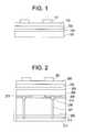
- FIG. 1is a cross-sectional diagram of the top layers of an electrostatic chuck in accordance with an embodiment of the invention.
- FIG. 2is a cross-sectional diagram showing further layers of an electrostatic chuck in accordance with an embodiment of the invention.
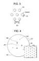
- FIG. 3is an illustration of a pattern of protrusions on the surface of an electrostatic chuck in accordance with an embodiment of the invention.
- FIG. 4is a diagram of the surface appearance of an electrostatic chuck in accordance with an embodiment of the invention.
- FIG. 5is a diagram illustrating lift pins raising a substrate having a thick oxide or nitride insulating layer off the surface of a prior art electrostatic chuck.
- FIG. 6is a diagram of a substrate having a thick oxide or nitride insulating layer, as the substrate is rising off the surface of an electrostatic chuck in accordance with an embodiment of the invention.
- FIG. 7is a diagram of a substrate having a thick oxide or nitride insulating layer, as the substrate is rising off the surface of a prior art electrostatic chuck.
- an electrostatic chuckthat includes a charge control surface layer having a high surface resistivity, for example greater than about 10 11 ohms per square, including greater than about 10 12 ohms per square and greater than about 10 13 ohms per square.
- a charge control surface layer having such high surface resistivitieshas been found to prevent wafer sticking to the electrostatic chuck while not interfering with the electrostatic attraction between the electrostatic chuck and the substrate.
- a high surface resistivity charge control surface layermay be produced by altering the surface resistivity of a surface layer that initially has a lower surface resistivity, for example by reactive ion etching, including plasma treatment, chemical treatment and/or rehydrogenation treatment.
- the high surface resistivity of a charge control surface layer in accordance with an embodiment of the inventionhelps to counteract the impact of a triboelectric effect between the electrostatic chuck and the substrate.
- Thismay be a particular problem where substrates are coated with thick insulator coatings.
- Substrates coated with a thick insulatorcan tend to stick to the electrostatic clamping surface, which can result in wafer handling problems and even the need to scrap wafers. Such problems can occur with both electrostatic and mechanical clamping systems.
- controlling the surface resistivity of the clamp surface to a high surface resistivityis believed to minimize the impact of triboelectric charging of substrate and clamp during the dechucking of the insulator coated substrate.
- a high surface resistivitymay be used for both electrostatic and mechanical clamping systems.
- wafer stickingmay be prevented without modifying the functioning of the clamp, such as without modifying the power supply, electrode structure, dielectric thickness, mechanical properties and/or clamping force, as is done in other techniques of preventing wafer sticking.
- FIG. 1is a cross-sectional diagram of the top layers of an electrostatic chuck in accordance with an embodiment of the invention.
- the electrostatic chuckmay feature protrusions 101 on its surface for mounting a substrate.
- the electrostatic chuckfeatures a charge control surface layer 102 , to which the protrusions 101 may adhere.
- the purpose of the charge control layer 102is to provide a conductive layer to bleed away surface charge.
- the charge control layer 102reduces the likelihood of wafer sticking.
- a charge control layer 102 having a surface resistivity in an appropriate rangesuch as, for example, greater than about 10 11 ohms per square, including greater than about 10 12 ohms per square, greater than about 10 13 ohms per square, and/or a range of from about 1 ⁇ 10 11 ohms/square to about 1 ⁇ 10 16 ohms/square, and/or a range of from about 1 ⁇ 10 12 ohms/square to about 1 ⁇ 10 16 ohms/square, and/or a range of from about 1 ⁇ 10 13 ohms/square to about 1 ⁇ 10 16 ohms/square, reduces wafer sticking.
- the slightly conductive surface layerbleeds charge to ground (not shown) while not interfering with the electrostatic attraction between the electrostatic chuck and the substrate.
- An adhesive layer 103may be underneath the charge control layer 102 . Alternatively, the adhesive layer 103 need not be present. Underneath the adhesive layer 103 (or directly underneath the charge control layer 102 ), the electrostatic chuck may include an adhesion coating 104 that encourages the layers above it to adhere to the dielectric layer 105 .
- the adhesion coating 104may, for example, include silicon containing nitrides, oxides, carbides and non-stoichiometric versions of these, for example but not limited to SiO x N y , silicon nitride, silicon oxide or silicon carbide.
- the adhesion coating layermay also comprise carbon or a nitride compound of carbon; and may comprise diamond-like carbon; and/or a combination of any of the foregoing.
- a dielectric layer 105such as an alumina dielectric.
- surface layerincludes a charge control layer 102 and any protrusions 101 that are present in the electrostatic chuck.
- the protrusions 101may be formed of a polymer, such as polyetherimide (PEI), polyimide or polyether ether ketone (PEEK).
- the charge control surface layer 102may be formed of the same polymer substance as the protrusions 101 , such as polyetherimide (PEI), polyimide or polyether ether ketone (PEEK).
- the charge control surface layer 102 and protrusions 101may also be formed of different materials. The protrusions and charge control surface layer may assist with encouraging contact of the electrostatic chuck with the substrate to promote contact cooling, while also reducing production of undesirable particles.
- the gas seal rings (not shown) of the electrostatic chuckmay be formed of a polymer, such as the same polymer as the protrusions 101 .
- the adhesive layer 103may comprise a different polymer from the charge control layer 102 .
- the charge control layer 102is formed of polyether ether ketone (PEEK)
- the adhesive layer 103may comprise polyetherimide (PEI).
- the charge control surface layer 102 and/or any protrusions 101 in the chuckneed not include a polymer, and may be formed of silicon containing nitrides, oxides, carbides and non-stoichiometric versions of these, for example but not limited to SiO x N y , silicon nitride, silicon oxide or silicon carbide.
- the ratio of silicon to other substances in the charge control surface layer 102may be controlled in order to achieve a desired level of high surface resistivity, including by using an increased ratio of silicon to other substances in order to increase the surface resistivity and/or a decreased ratio of silicon to other substances in order to decrease the surface resistivity.
- the charge control surface layer 102may also comprise carbon or a nitride compound of carbon; and may comprise diamond-like carbon; and/or a combination of any of the foregoing. Other substances having surface resistivities in the desired range may be used for the charge control surface layer 102 .
- FIG. 2is a cross-sectional diagram showing further layers of an electrostatic chuck in accordance with an embodiment of the invention.
- the electrostatic chuckincludes metal electrodes 206 .
- the metal electrodes 206are bonded to electrode pins 207 by electrically conductive epoxy bonds 208 .
- the dielectric layer 205is bonded to a insulator layer 209 , such as an alumina insulator, by a ceramic to ceramic bond 210 .
- the ceramic to ceramic bond 210may be formed of a polymer, such as polytetrafluoroethylene (PTFE) or modified PTFE (which includes PFA and/or FEP in addition to PTFE). Further, the ceramic to ceramic bond 210 may be formed of polymers such as perfluoroalkoxy (PFA), fluorinated ethylene-propylene (FEP) and polyether ether ketone (PEEK). Underneath the insulator 209 there is a thermally conductive bond 211 (which may be formed, for example, using TRA-CON thermally conductive epoxy, sold by TRA-CON, Inc. of Bedford, Mass., U.S.A.) and a water cooled base 212 .
- TRA-CON thermally conductive epoxysold by TRA-CON, Inc. of Bedford, Mass., U.S.A.
- the adhesion coating 204may extend down an edge of the electrostatic chuck (including down the edges of the gas seal rings) to form a metals reduction layer 213 , which prevents beam strikes on the edges of the electrostatic chuck from causing aluminum particles to strike the substrate.
- the polyetherimide (PEI) used for the protrusions 201 , charge control layer 202 or other components of the electrostatic chuckmay be formed of unfilled amorphous polyether imide (PEI), in a thickness of between about 12 microns and about 25 microns.
- PEIunfilled amorphous polyether imide
- PEI sold under the tradename ULTEM 1000may be used, sold by Sabic Innovative Plastics Holdings BV.
- the protrusions 201 and/or charge control layer 202 or other componentsare formed of polyether ether ketone (PEEK), they may be made from unfilled PEEK, in a thickness of between about 12 microns and about 25 microns.
- PEEK sold under the trade name Victrex® APTIV PEEKTM FILM, 2000-006(unfilled amorphous grade) may be used, sold by Victrex U.S.A., Inc. of West Conshohocken, Pa., U.S.A.
- An electrostatic chuck in accordance with an embodiment of the inventionmay include features of the electrostatic chuck of U.S. patent application Ser. No. 12/454,336, filed on May 15, 2009, published as U.S. Patent Application Publication No. 2009/0284894, the teachings of which are hereby incorporated by reference in their entirety.
- features relating to equally spaced protrusions, trigonal pattern protrusions and low particle productionmay be included, and other features may also be included.
- an electrostatic chuck in accordance with an embodiment of the inventionmay include features of the electrostatic chuck of PCT Application PCT/US2010/034667, filed on May 13, 2010, entitled “Electrostatic Chuck With Polymer Protrusions,” the teachings of which are hereby incorporated by reference in their entirety.
- features relating to polymer protrusions and charge control layersmay be included, and other features may also be included.
- FIG. 3is an illustration of a pattern of protrusions 314 on the surface of an electrostatic chuck, in accordance with an embodiment of the invention, in which the protrusion pattern is used to reduce the forces between a substrate and the protrusions 314 .
- Protrusion patterns that equally distribute such forcesmay be used, for example trigonal or generally hexagonal patterns of protrusions. It should be appreciated that, as used herein, a “trigonal” pattern is intended to mean a regularly repeating pattern of equilateral triangles of protrusions, such that the protrusions are substantially equally spaced apart.
- a patternmay also be viewed as being generally hexagonal in shape, with a central protrusion in the center of an array of six protrusions that form the vertices of a regular hexagon). Forces may also be reduced by increasing the diameter 315 of the protrusions, or by decreasing the center-to-center spacing 316 of the protrusions 314 . As shown in the embodiment of FIG. 3 , the protrusions may be disposed in an equally spaced arrangement, in which each protrusion is substantially equally spaced apart from the adjacent protrusions by a center to center spacing dimension 316 .
- the substratemay contact greater than 25% of the protrusion's top surface area.
- the electrostatic chuckmay be a 300 mm configuration, including an aluminum base, an alumina insulator 209 of about 0.120 inches in thickness, an alumina dielectric 205 of about 0.004 inches thickness, and having a rotary platen design to allow rotating and tilting of the substrate that is mounted to the electrostatic chuck.
- the diameter of the electrostatic chuckmay, for example, be 300 mm, 200 mm or 450 mm.
- the protrusions 314may be in a trigonal pattern, with a center to center spacing dimension 316 of from about 6 mm to about 8 mm, for example.
- the diameter 315 of the protrusionsmay, for example, be about 900 microns.
- the height of the protrusions 314may, for example, be from about 3 microns to about 12 microns, such as about 6 microns.
- the protrusions 314may be formed entirely of polymer, as may be the charge control layer 202 (see FIG. 2 ).
- FIG. 4is a diagram of the surface appearance of an electrostatic chuck in accordance with an embodiment of the invention.
- the electrostatic chuck surfaceincludes gas inlets 417 , a ground pin passage 418 , a gas seal ring 419 , a lift pin passage 420 that includes its own gas seal ring (outer light-colored structure of lift pin passage 420 in FIG. 4 ), and a small gas inlet at 421 in the center of the chuck (inlet not visible in FIG. 4 ).
- the ground pin passage 418may include its own gas seal ring (outer ring of ground pin passage 419 in FIG. 4 ).
- a detail view (inset 422 in FIG. 4 )shows the protrusions 414 .
- the gas seal ring 419(and the gas seal rings of the lift pin passages 420 and ground pin passages 418 ) may be about 0.1 inches in width and may have an equal height to that of the protrusions 414 , such as from about 3 microns to about 12 microns, for example about 6 microns, although other widths and heights are possible.
- an electrostatic chuckmay be made by the process of, first, preparing the ceramic assembly using a ceramic to ceramic bond.
- the dielectric layer 205may be bonded to the insulator layer 209 using the bonding substances described above in connection with the embodiment of FIG. 2 .
- the ceramic assemblyis coated with the adhesion coating 204 , such as the substances discussed above in connection with the embodiment of FIG. 1 , to a thickness of about 1 or 2 microns.
- the polymer substance that will make up the charge control layer 202 and protrusions 201is bonded to the surface of the adhesion coating 204 .
- the top of the polymer substancemay then be plasma treated to help photoresist (applied next) to stick.
- photoresistis deposited on the polymer substance, and is exposed and developed.
- a reactive ion etch processis used to remove a thickness of the polymer substance (such as between about 3 microns and about 12 microns, in particular about 6 microns) to create the areas between the protrusions 201 .
- the amount etched awaymay be optimized for the back side gas pressure that will be used with the electrostatic chuck.
- the height of the protrusionsis preferably approximately the same as, or substantially equal to, the mean free path of the gas used in back side cooling. After etching, the photoresist is then stripped off.
- a high surface resistivity charge control surface layermay be produced by altering the surface resistivity of the surface layer that has been produced.
- the surface layermay be altered to have a higher surface resistivity by treating the surface layer that has been produced with reactive ion etching, including plasma treatment, chemical treatment and/or rehydrogenation treatment.
- the plasma treatmentmay be an oxygen plasma treatment.
- the processmay proceed to final assembly of the electrostatic chuck.
- a high surface resistivity charge control surface layermay be produced by altering the surface resistivity of a surface layer that initially has a lower surface resistivity.
- the altering of the surface resistivitymay produce a surface resistivity after treatment that is within plus or minus 25% of what the surface resistivity would have been prior to treatment.
- the altering of the surface resistivitymay be performed after the lower surface resistivity surface layer has been patterned.
- the initial lower surface resistivity surface layermay include a polymer, such as polyetherimide (PEI), polyimide or polyether ether ketone (PEEK).
- the initial lower surface resistivity surface layermay include silicon containing nitrides, oxides, carbides and non-stoichiometric versions of these, for example but not limited to SiO x N y , silicon nitride, silicon oxide or silicon carbide.
- the initial lower surface resistivity surface layermay also comprise carbon or a nitride compound of carbon; and may comprise diamond-like carbon; and/or a combination of any of the foregoing.
- an initially formed surface layermay be treated by any of the processes described above, such as reactive ion etching, to achieve a surface resistivity of greater than about 10 11 ohms per square, including greater than about 10 12 ohms per square, greater than about 10 13 ohms per square, and/or a range from about 1 ⁇ 10 11 ohms/square to about 1 ⁇ 10 16 ohms/square, and/or a range of from about 1 ⁇ 10 12 ohms/square to about 1 ⁇ 10 16 ohms/square, and/or a range of from about 1 ⁇ 10 13 ohms/square to about 1 ⁇ 10 16 ohms/square.
- the surface resistivitymay be measured according to the standards set forth in ASTM Standard D257-07, entitled “Standard Test Methods for DC Resistance or Conductance of Insulating Materials,” published by ASTM International of West Conshohocken, Pa., U.S.A., the entire disclosure of which is hereby incorporated herein by reference.
- the surface resistivitymay be measured on the surface of the electrostatic chuck to which a substrate is clamped, using a standard surface resistivity probe, for example a TREK circular probe, sold by TREK, Inc. of Medina, N.Y., U.S.A.
- the surface resistivitymay be measured either on the area of the surface that is between the protrusions or on the surface of the protrusions.
- surface resistivities greater than about 10 14 ohms per squarephysisorbed water can affect the measurement of surface resistivity, and measurement in a dry environment or vacuum is therefore preferably used.
- a higher surface resistivity layermay also be applied to an electrostatic chuck directly, without modifying an initially lower surface resistivity layer.
- a higher surface resistivity layermay be applied after first removing at least part of an initially lower surface resistivity layer using an etching process, such as a reactive ion etch process.
- an etching processsuch as a reactive ion etch process.
- an initial lower surface resistivity surface layerincludes silicon containing nitrides, oxides, carbides and non-stoichiometric versions of these, a portion of the surface layer may be removed by a reactive ion etch process until an insulator layer of the electrostatic chuck is exposed, and then a higher surface resistivity coating may be applied.
- FIG. 5is a diagram illustrating the raising of a substrate 523 having a thick oxide or nitride insulating layer off the surface of a prior art electrostatic chuck 524 .
- Triboelectric chargingis the process of electron transfer as a result of two objects coming into contact with each other and then separating.
- the prefix “tribo”means “to rub.” The process of triboelectric charging results in one object gaining electrons on its surface, and therefore becoming negatively charged, and another object losing electrons from its surface, and therefore becoming positively charged.
- FIG. 6is a diagram of a substrate 623 having a thick oxide or nitride insulating layer 627 , as the substrate 623 is rising off the surface of an electrostatic chuck 624 in accordance with an embodiment of the invention.
- a substrate 623will never lift off exactly parallel from the surface of the electrostatic chuck 624 , and there will therefore be a last point of contact 628 between the substrate 623 and the electrostatic chuck 624 .
- the last point of contact 628could be the point of wafer sticking.
- a high resistivity surface 629has positive charges 630 left on its surface that are not mobile.
- Negative charges in the oxide or nitride insulating layer 627 of the substrateare likewise not mobile.
- the surface of the chuck 624 and the surface of the substrate 623are charged with opposite polarity, but the charges are randomly placed and spread out, and thus too weak to cause significant wafer sticking. Accordingly, a high resistivity surface 629 in accordance with an embodiment of the invention helps to prevent wafer sticking.
- FIG. 7is a diagram of a substrate 723 having a thick oxide or nitride insulating layer 727 , as the substrate 723 is rising off the surface of a prior art electrostatic chuck 724 .
- the electrostatic chuck 724has a lower surface resistivity surface 729 .
- Both the negative charges 731 in the substrate 723 and the positive charges 730 in the lower resistivity surface 729are mobile; a separation of charge 732 occurs in the substrate 723 and the charges 731 and 730 migrate towards the last point of contact 728 to form a strong capacitor, thereby sticking the corner of the substrate 723 to the electrostatic chuck 724 .
- the surface resistivity of an electrostatic chuckcould be effectively lowered in use when arsenic and/or phosphorus are ejected from a heated graphite target upon which a conductive beam is being directed.
- the ejected arsenic and/or phosphoruscan be deposited and condensed on the surface of the cooled electrostatic chuck, thereby lowering its surface resistivity and potentially resulting in subsequent wafer sticking.
- a surface resistivity in accordance with an embodiment of the inventionshould be high enough not to be reduced to an undesirably low level of surface resistivity by the effect of such beam deposits.
- experimentswere performed with oxide/nitride coated wafers using electrostatic chucks having low resistivity surfaces and high resistivity surfaces, as shown in Table 1 below.
- Surface resistivitieswere measured using a TREK circular probe, sold by TREK, Inc. of Medina, N.Y., U.S.A.
- the oxide wafersstuck to all of the low surface resistivity electrostatic chucks, and normal wafer cycling was not possible. However, the oxide wafers did not stick to any of the high surface resistivity electrostatic chucks.
- An embodiment according to the inventiontherefore exhibited success in mitigating wafer sticking.
- an electrostatic chuckmay include protrusions having a height of about 6 microns, and having a very smooth wafer contact surface.
- the protrusionmay have a surface roughness on the wafer contact surface of about 0.02 ⁇ m to about 0.05 ⁇ m.
- the gas seal ringsmay have a similarly smooth surface, which results in a good seal with the substrate.
- the gas seal rings of the electrostatic chuckmay comprise a surface roughness of less than about 8 microinches, or less than about 4 microinches, or less than about 2 microinches, or less than about 1 microinches.
- the electrostatic chuckis a Coulombic chuck.
- the dielectriccan include aluminum, for example alumina or aluminum nitride.
- the electrostatic chuckis a Johnsen-Rahbek electrostatic chuck.
- the electrostatic chuckmay not be a Johnsen-Rahbek electrostatic chuck, and the dielectric may be chosen so that a Johnsen-Rahbek (JR) force or partial hybrid Johnsen-Rahbek force does not act on the wafer or substrate.
- JRJohnsen-Rahbek
Landscapes
- Engineering & Computer Science (AREA)
- Chemical & Material Sciences (AREA)
- Ceramic Engineering (AREA)
- Organic Chemistry (AREA)
- Materials Engineering (AREA)
- Mechanical Engineering (AREA)
- Structural Engineering (AREA)
- Physics & Mathematics (AREA)
- General Physics & Mathematics (AREA)
- Condensed Matter Physics & Semiconductors (AREA)
- Computer Hardware Design (AREA)
- Power Engineering (AREA)
- Microelectronics & Electronic Packaging (AREA)
- Manufacturing & Machinery (AREA)
- Chemical Kinetics & Catalysis (AREA)
- General Chemical & Material Sciences (AREA)
- Metallurgy (AREA)
- Container, Conveyance, Adherence, Positioning, Of Wafer (AREA)
- Jigs For Machine Tools (AREA)
Abstract
Description
| TABLE 1 |
| Comparison of Wafer Sticking for Differing Surface Resistivities |
| Measured Platen | |||
| Surface Resistivity | Expected | Observed | |
| in Ohms/Square | Wafer Type | Result | Result |
| 1014 | Oxide/Nitride | No Wafer | No Wafer |
| 800A/200A | Sticking | Sticking | |
| 1010 | Oxide/Nitride | Wafer | Wafer |
| 800A/200A | Sticking | Sticking | |
Claims (14)
Priority Applications (1)
| Application Number | Priority Date | Filing Date | Title |
|---|---|---|---|
| US13/699,279US9025305B2 (en) | 2010-05-28 | 2011-05-24 | High surface resistivity electrostatic chuck |
Applications Claiming Priority (3)
| Application Number | Priority Date | Filing Date | Title |
|---|---|---|---|
| US34950410P | 2010-05-28 | 2010-05-28 | |
| PCT/US2011/037712WO2011149918A2 (en) | 2010-05-28 | 2011-05-24 | High surface resistivity electrostatic chuck |
| US13/699,279US9025305B2 (en) | 2010-05-28 | 2011-05-24 | High surface resistivity electrostatic chuck |
Publications (2)
| Publication Number | Publication Date |
|---|---|
| US20130070384A1 US20130070384A1 (en) | 2013-03-21 |
| US9025305B2true US9025305B2 (en) | 2015-05-05 |
Family
ID=45004704
Family Applications (1)
| Application Number | Title | Priority Date | Filing Date |
|---|---|---|---|
| US13/699,279ActiveUS9025305B2 (en) | 2010-05-28 | 2011-05-24 | High surface resistivity electrostatic chuck |
Country Status (6)
| Country | Link |
|---|---|
| US (1) | US9025305B2 (en) |
| JP (1) | JP6014587B2 (en) |
| KR (1) | KR101731136B1 (en) |
| CN (2) | CN102986017B (en) |
| TW (2) | TWI545683B (en) |
| WO (1) | WO2011149918A2 (en) |
Cited By (3)
| Publication number | Priority date | Publication date | Assignee | Title |
|---|---|---|---|---|
| US9543187B2 (en) | 2008-05-19 | 2017-01-10 | Entegris, Inc. | Electrostatic chuck |
| US9721821B2 (en) | 2009-05-15 | 2017-08-01 | Entegris, Inc. | Electrostatic chuck with photo-patternable soft protrusion contact surface |
| US11387135B2 (en) | 2016-01-28 | 2022-07-12 | Applied Materials, Inc. | Conductive wafer lift pin o-ring gripper with resistor |
Families Citing this family (18)
| Publication number | Priority date | Publication date | Assignee | Title |
|---|---|---|---|---|
| WO2010132640A2 (en) | 2009-05-15 | 2010-11-18 | Entegris, Inc. | Electrostatic chuck with polymer protrusions |
| KR101731136B1 (en) | 2010-05-28 | 2017-04-27 | 엔테그리스, 아이엔씨. | High surface resistivity electrostatic chuck |
| KR102127883B1 (en)* | 2012-11-02 | 2020-06-29 | 엔테그리스, 아이엔씨. | Electrostatic chuck with photo-patternable soft protrusion contact surface |
| JP6173936B2 (en)* | 2013-02-28 | 2017-08-02 | 東京エレクトロン株式会社 | Mounting table and plasma processing apparatus |
| WO2015120265A1 (en) | 2014-02-07 | 2015-08-13 | Entegris, Inc. | Electrostatic chuck and method of making same |
| US10325800B2 (en)* | 2014-08-26 | 2019-06-18 | Applied Materials, Inc. | High temperature electrostatic chucking with dielectric constant engineered in-situ charge trap materials |
| KR101614370B1 (en) | 2015-04-07 | 2016-04-21 | 엘지전자 주식회사 | Semiconductor light emitting device, transfer head of the semiconductor light emitting device, and method for transferring the semiconductor light emitting device |
| KR20170039781A (en)* | 2015-10-01 | 2017-04-12 | 삼성디스플레이 주식회사 | Electrostatic chuck and substrate processing apparatus including the same |
| KR101651912B1 (en)* | 2016-02-02 | 2016-09-09 | 주식회사 테스 | Susceptor and substrate processing apparatus having the same |
| US11289355B2 (en) | 2017-06-02 | 2022-03-29 | Lam Research Corporation | Electrostatic chuck for use in semiconductor processing |
| US11469084B2 (en) | 2017-09-05 | 2022-10-11 | Lam Research Corporation | High temperature RF connection with integral thermal choke |
| US11990360B2 (en) | 2018-01-31 | 2024-05-21 | Lam Research Corporation | Electrostatic chuck (ESC) pedestal voltage isolation |
| US11086233B2 (en)* | 2018-03-20 | 2021-08-10 | Lam Research Corporation | Protective coating for electrostatic chucks |
| US11183368B2 (en) | 2018-08-02 | 2021-11-23 | Lam Research Corporation | RF tuning systems including tuning circuits having impedances for setting and adjusting parameters of electrodes in electrostatic chucks |
| US20200058539A1 (en)* | 2018-08-17 | 2020-02-20 | Applied Materials, Inc. | Coating material for processing chambers |
| TW202408972A (en) | 2019-10-02 | 2024-03-01 | 日商佳能股份有限公司 | Wafer chuck, method for producing the same, and exposure apparatus |
| DE102021206512A1 (en)* | 2021-06-24 | 2022-12-29 | Carl Zeiss Smt Gmbh | Method for forming a knob structure, holding device for electrostatically holding a component, and EUV lithography system |
| JP2024146003A (en)* | 2023-03-31 | 2024-10-15 | ホヤ レンズ タイランド リミテッド | Eyeglass lenses and spectacles |
Citations (169)
| Publication number | Priority date | Publication date | Assignee | Title |
|---|---|---|---|---|
| US4184188A (en) | 1978-01-16 | 1980-01-15 | Veeco Instruments Inc. | Substrate clamping technique in IC fabrication processes |
| JPH0227748A (en) | 1988-07-16 | 1990-01-30 | Tomoegawa Paper Co Ltd | Electrostatic chucking device and forming method therefor |
| JPH02304946A (en) | 1989-05-19 | 1990-12-18 | Mitsui Petrochem Ind Ltd | electrostatic chuck |
| US5179498A (en) | 1990-05-17 | 1993-01-12 | Tokyo Electron Limited | Electrostatic chuck device |
| US5250137A (en) | 1990-07-20 | 1993-10-05 | Tokyo Electron Limited | Plasma treating apparatus |
| US5310453A (en) | 1992-02-13 | 1994-05-10 | Tokyo Electron Yamanashi Limited | Plasma process method using an electrostatic chuck |
| US5350479A (en) | 1992-12-02 | 1994-09-27 | Applied Materials, Inc. | Electrostatic chuck for high power plasma processing |
| US5382311A (en) | 1992-12-17 | 1995-01-17 | Tokyo Electron Limited | Stage having electrostatic chuck and plasma processing apparatus using same |
| US5413360A (en) | 1992-12-01 | 1995-05-09 | Kyocera Corporation | Electrostatic chuck |
| US5539609A (en) | 1992-12-02 | 1996-07-23 | Applied Materials, Inc. | Electrostatic chuck usable in high density plasma |
| US5557215A (en) | 1993-05-12 | 1996-09-17 | Tokyo Electron Limited | Self-bias measuring method, apparatus thereof and electrostatic chucking apparatus |
| US5583736A (en) | 1994-11-17 | 1996-12-10 | The United States Of America As Represented By The Department Of Energy | Micromachined silicon electrostatic chuck |
| US5591269A (en) | 1993-06-24 | 1997-01-07 | Tokyo Electron Limited | Vacuum processing apparatus |
| US5625526A (en) | 1993-06-01 | 1997-04-29 | Tokyo Electron Limited | Electrostatic chuck |
| US5656093A (en) | 1996-03-08 | 1997-08-12 | Applied Materials, Inc. | Wafer spacing mask for a substrate support chuck and method of fabricating same |
| US5691876A (en) | 1995-01-31 | 1997-11-25 | Applied Materials, Inc. | High temperature polyimide electrostatic chuck |
| US5701228A (en) | 1995-03-17 | 1997-12-23 | Tokyo Electron Limited | Stage system or device |
| US5740009A (en) | 1996-11-29 | 1998-04-14 | Applied Materials, Inc. | Apparatus for improving wafer and chuck edge protection |
| US5748434A (en) | 1996-06-14 | 1998-05-05 | Applied Materials, Inc. | Shield for an electrostatic chuck |
| US5761023A (en) | 1996-04-25 | 1998-06-02 | Applied Materials, Inc. | Substrate support with pressure zones having reduced contact area and temperature feedback |
| US5764471A (en) | 1996-05-08 | 1998-06-09 | Applied Materials, Inc. | Method and apparatus for balancing an electrostatic force produced by an electrostatic chuck |
| US5777838A (en) | 1995-12-19 | 1998-07-07 | Fujitsu Limited | Electrostatic chuck and method of attracting wafer |
| US5779803A (en) | 1993-12-24 | 1998-07-14 | Tokyo Electron Limited | Plasma processing apparatus |
| US5792562A (en) | 1995-01-12 | 1998-08-11 | Applied Materials, Inc. | Electrostatic chuck with polymeric impregnation and method of making |
| US5825607A (en) | 1996-05-08 | 1998-10-20 | Applied Materials, Inc. | Insulated wafer spacing mask for a substrate support chuck and method of fabricating same |
| US5851298A (en) | 1996-02-01 | 1998-12-22 | Tokyo Electron Limited | Susceptor structure for mounting processing object thereon |
| US5868848A (en) | 1995-06-07 | 1999-02-09 | Tokyo Electron Limited | Plasma processing apparatus |
| US5870271A (en) | 1997-02-19 | 1999-02-09 | Applied Materials, Inc. | Pressure actuated sealing diaphragm for chucks |
| US5880924A (en) | 1997-12-01 | 1999-03-09 | Applied Materials, Inc. | Electrostatic chuck capable of rapidly dechucking a substrate |
| US5886866A (en) | 1998-07-06 | 1999-03-23 | Applied Materials, Inc. | Electrostatic chuck having a combination electrode structure for substrate chucking, heating and biasing |
| US5886865A (en) | 1998-03-17 | 1999-03-23 | Applied Materials, Inc. | Method and apparatus for predicting failure of an eletrostatic chuck |
| WO1999016122A1 (en) | 1997-09-25 | 1999-04-01 | Applied Materials, Inc. | Hybrid johnsen-rahbek electrostatic chuck and method of fabricating same |
| US5914568A (en) | 1997-03-19 | 1999-06-22 | Tokyo Electron Limited | Plasma processing apparatus |
| JPH11214494A (en) | 1998-01-26 | 1999-08-06 | Taiheiyo Cement Corp | Electrostatic chuck |
| US5946184A (en) | 1996-09-19 | 1999-08-31 | Hitachi, Ltd. | Electrostatic chuck, and method of and apparatus for processing sample |
| US5946183A (en) | 1995-09-06 | 1999-08-31 | Ngk Insulators, Ltd. | Electrostatic chuck |
| WO1999025006A3 (en) | 1997-11-06 | 1999-10-28 | Applied Materials Inc | Electrostatic chuck having improved gas conduits |
| WO1999054928A1 (en) | 1998-04-21 | 1999-10-28 | Applied Materials, Inc. | Electrostatic chuck formed by integral ceramic and metal sintering |
| WO1999057753A1 (en) | 1998-05-01 | 1999-11-11 | Applied Materials, Inc. | Apparatus for improved biasing and retaining of a workpiece in a workpiece processing system |
| WO1999062115A1 (en) | 1998-05-22 | 1999-12-02 | Applied Materials, Inc. | Electrostatic chuck having an electrical connector with housing |
| US5997962A (en) | 1995-06-30 | 1999-12-07 | Tokyo Electron Limited | Plasma process utilizing an electrostatic chuck |
| WO1999060613A3 (en) | 1998-05-21 | 2000-01-20 | Applied Materials Inc | Method and apparatus for minimizing plasma destabilization within a semiconductor wafer processing system |
| US6028762A (en) | 1996-01-31 | 2000-02-22 | Kyocera Corporation | Electrostatic chuck |
| WO1999052144A9 (en) | 1998-04-03 | 2000-02-24 | Applied Materials Inc | Electrostatic chuck power supply |
| WO2000019592A1 (en) | 1998-09-30 | 2000-04-06 | Lam Research Corporation | Dechucking method and apparatus for workpieces in vacuum processors |
| JP2000100917A (en) | 1998-09-22 | 2000-04-07 | Jeol Ltd | Electrostatic chuck device |
| US6051122A (en) | 1997-08-21 | 2000-04-18 | Applied Materials, Inc. | Deposition shield assembly for a semiconductor wafer processing system |
| US6055150A (en) | 1996-05-02 | 2000-04-25 | Applied Materials, Inc. | Multi-electrode electrostatic chuck having fuses in hollow cavities |
| WO2000019519B1 (en) | 1998-09-30 | 2000-05-25 | Lam Res Corp | Electrostatic dechucking method and apparatus for dielectric workpieces in vacuum processors |
| WO2000035003A1 (en) | 1998-12-10 | 2000-06-15 | Applied Materials, Inc. | Apparatus and method for actively controlling surface potential of an electrostatic chuck |
| US6088213A (en) | 1997-07-11 | 2000-07-11 | Applied Materials, Inc. | Bipolar electrostatic chuck and method of making same |
| US6104595A (en) | 1998-04-06 | 2000-08-15 | Applied Materials, Inc. | Method and apparatus for discharging an electrostatic chuck |
| US6117246A (en) | 1997-01-31 | 2000-09-12 | Applied Materials, Inc. | Conductive polymer pad for supporting a workpiece upon a workpiece support surface of an electrostatic chuck |
| US6175485B1 (en) | 1996-07-19 | 2001-01-16 | Applied Materials, Inc. | Electrostatic chuck and method for fabricating the same |
| US6217655B1 (en) | 1997-01-31 | 2001-04-17 | Applied Materials, Inc. | Stand-off pad for supporting a wafer on a substrate support chuck |
| US20010003298A1 (en)* | 1999-06-09 | 2001-06-14 | Shamouil Shamouilian | Substrate support for plasma processing |
| WO2001042163A2 (en) | 1999-12-09 | 2001-06-14 | Saint-Gobain Ceramics & Plastics, Inc. | High-purity low-resistivity electrostatic chucks |
| US6259592B1 (en) | 1998-11-19 | 2001-07-10 | Applied Materials, Inc. | Apparatus for retaining a workpiece upon a workpiece support and method of manufacturing same |
| USRE37294E1 (en) | 1994-03-03 | 2001-07-24 | Diamonex, Incorporated | Ion beam process for deposition of highly abrasion-resistant coatings |
| EP1119040A2 (en) | 2000-01-20 | 2001-07-25 | Ngk Insulators, Ltd. | Electrostatic wafer chuck |
| US6304424B1 (en) | 1998-04-03 | 2001-10-16 | Applied Materials Inc. | Method and apparatus for minimizing plasma destabilization within a semiconductor wafer processing system |
| US20010055190A1 (en) | 2000-04-27 | 2001-12-27 | Nhk Spring Co., Ltd. | Electrostatic chuck |
| US20020000521A1 (en) | 2000-04-19 | 2002-01-03 | Karl Brown | Method and apparatus for conditioning an electrostatic chuck |
| US6338861B1 (en) | 1998-03-26 | 2002-01-15 | Shiseido Company, Ltd. | Process of production of natural flavor or fragrance |
| US20020008954A1 (en) | 1999-04-19 | 2002-01-24 | Karl F. Leeser | Method and apparatus for controlling chucking force in an electrostatic |
| US20020012219A1 (en) | 2000-05-19 | 2002-01-31 | Ngk Insulators, Ltd. | Electrostatic chucks and electrostatically adsorbing structures |
| US20020021545A1 (en) | 2000-08-16 | 2002-02-21 | Creative Technology Corp. | Electrostatic chucking device and manufacturing method thereof |
| US20020027762A1 (en) | 1998-09-29 | 2002-03-07 | Shinji Yamaguchi | Electrostatic chuck |
| US20020036373A1 (en) | 2000-06-02 | 2002-03-28 | Sumitomo Osaka Cement Co., Ltd. | Holding apparatus for clamping a workpiece |
| WO2002031219A1 (en) | 2000-10-06 | 2002-04-18 | Lam Research Corporation | Electrostatically clamped edge ring for plasma processing |
| JP2002141404A (en) | 2000-10-31 | 2002-05-17 | Kyocera Corp | Electrode built-in body and wafer support member using the same |
| US6433346B1 (en) | 1999-10-19 | 2002-08-13 | Nikon Corporation | Electrostatic reticle chucks, charged-particle-beam microlithography apparatus and methods, and semiconductor-device manufacturing methods comprising same |
| US20020109955A1 (en) | 2000-12-11 | 2002-08-15 | Shinsuke Masuda | Electrostatic chuck and method of manufacturing the same |
| US6441939B1 (en) | 1997-05-07 | 2002-08-27 | Alcatel | Device and method for regenerating a train of solitons |
| US6452775B1 (en) | 2000-03-31 | 2002-09-17 | Lam Research Corporation | Electrostatic chuck and method for manufacturing the same |
| US20020130276A1 (en) | 2001-03-13 | 2002-09-19 | Michael Sogard | Gas cooled electrostatic pin chuck for vacuum applications |
| US20020144786A1 (en) | 2001-04-05 | 2002-10-10 | Angstron Systems, Inc. | Substrate temperature control in an ALD reactor |
| US20020144657A1 (en) | 2001-04-05 | 2002-10-10 | Chiang Tony P. | ALD reactor employing electrostatic chuck |
| US20020146511A1 (en) | 2001-04-05 | 2002-10-10 | Chiang Tony P. | Chemisorption technique for atomic layer deposition |
| JP2002299425A (en) | 2001-03-29 | 2002-10-11 | Foi:Kk | Plasma processing equipment |
| US20020159217A1 (en) | 2001-01-29 | 2002-10-31 | Ngk Insulators, Ltd. | Electrostatic chuck and substrate processing apparatus |
| US20020158270A1 (en)* | 2001-04-25 | 2002-10-31 | Makoto Yamamoto | Lateral transistor having graded base region, semiconductor integrated circuit and fabrication method thereof |
| US20020167779A1 (en) | 2001-05-09 | 2002-11-14 | Carroll James C. | Method and apparatus for the grounding of process wafers by the use of conductive regions created by ion implantation into the surface of an electrostatic clamp |
| US6483690B1 (en) | 2001-06-28 | 2002-11-19 | Lam Research Corporation | Ceramic electrostatic chuck assembly and method of making |
| US20020170882A1 (en) | 2001-02-28 | 2002-11-21 | Fuminori Akiba | Method and apparatus for supporting substrate |
| US6490145B1 (en) | 2001-07-18 | 2002-12-03 | Applied Materials, Inc. | Substrate support pedestal |
| US20030010292A1 (en) | 2001-07-16 | 2003-01-16 | Applied Materials, Inc. | Electrostatic chuck with dielectric coating |
| US6522519B1 (en) | 1999-05-07 | 2003-02-18 | Nikon Corporation | Electrostatic chucking device and methods for holding microlithographic sample |
| JP2003060020A (en) | 2001-06-07 | 2003-02-28 | Komatsu Ltd | Electrostatic chuck device |
| US20030053283A1 (en) | 1999-06-17 | 2003-03-20 | Applied Materials, Inc. | Method and apparatus for balancing an electrostatic force produced by an electrostatic chuck |
| US20030123213A1 (en) | 2001-11-14 | 2003-07-03 | Sumitomo Osaka Cement Co. Ltd | Electrostatic chuck and manufacturing method therefor |
| US20030165043A1 (en) | 2002-02-27 | 2003-09-04 | Joseph Logan | Hybrid ceramic electrostatic clamp |
| US20030168439A1 (en) | 2002-03-05 | 2003-09-11 | Seiichiro Kanno | Wafer stage for wafer processing apparatus and wafer processing method |
| JP2003282688A (en) | 2002-03-27 | 2003-10-03 | Kyocera Corp | Electrostatic chuck |
| US6634177B2 (en) | 2002-02-15 | 2003-10-21 | Taiwan Semiconductor Manufacturing Co., Ltd. | Apparatus for the real-time monitoring and control of a wafer temperature |
| US6641939B1 (en) | 1998-07-01 | 2003-11-04 | The Morgan Crucible Company Plc | Transition metal oxide doped alumina and methods of making and using |
| JP2004022889A (en) | 2002-06-18 | 2004-01-22 | Anelva Corp | Electrostatic adsorption device |
| US20040040665A1 (en) | 2002-06-18 | 2004-03-04 | Anelva Corporation | Electrostatic chuck device |
| US20040055709A1 (en) | 2002-09-19 | 2004-03-25 | Applied Materials, Inc. | Electrostatic chuck having a low level of particle generation and method of fabricating same |
| WO2004027839A2 (en) | 2002-09-19 | 2004-04-01 | Applied Materials, Inc. | Electrostatic chuck having a low level of particle generation and method of fabricating same |
| US20040121192A1 (en) | 2002-12-23 | 2004-06-24 | Lacourse Brian C | ALN material and electrostatic chuck incorporating same |
| US20040124595A1 (en) | 2002-12-19 | 2004-07-01 | Nhk Spring Co., Ltd. | Electrostatic chuck and production method therefor |
| US20040131775A1 (en) | 2003-01-07 | 2004-07-08 | The Regents Of The University Of California. | Compliant layer chucking surface |
| WO2004059714A1 (en) | 2002-12-26 | 2004-07-15 | Nikon Corporation | Polishing device and method of producing semiconductor device |
| US20040173469A1 (en) | 2003-03-04 | 2004-09-09 | Ryujiro Udo | Plasma processing apparatus and method for manufacturing electrostatic chuck |
| US20040233608A1 (en) | 2003-05-21 | 2004-11-25 | Tokyo Electron Limited Of Tbs Broadcast Center | Apparatus and methods for compensating plasma sheath non-uniformities at the substrate in a plasma processing system |
| US20040233609A1 (en) | 2002-12-26 | 2004-11-25 | Kazuto Yoshida | Electrostatic chuck and its manufacturing method |
| US6839217B1 (en) | 1999-10-01 | 2005-01-04 | Varian Semiconductor Equipment Associates, Inc. | Surface structure and method of making, and electrostatic wafer clamp incorporating surface structure |
| US20050018377A1 (en) | 2003-07-24 | 2005-01-27 | Samsung Electronics Co., Ltd. | Electrostatic chuck |
| JP2005033125A (en) | 2003-07-11 | 2005-02-03 | Toto Ltd | Electrostatic chuck and device mounted with electrostatic chuck |
| US6853953B2 (en) | 2001-08-07 | 2005-02-08 | Tokyo Electron Limited | Method for characterizing the performance of an electrostatic chuck |
| US20050029244A1 (en) | 1999-08-12 | 2005-02-10 | Ibiden Co., Ltd. | Ceramic substrate, ceramic heater, electrostatic chuck and wafer prober for use in semiconductor producing and inspecting devices |
| US20050069726A1 (en) | 2003-09-30 | 2005-03-31 | Douglas Elliot Paul | Light emitting composite material and devices thereof |
| US20050079737A1 (en) | 2003-10-10 | 2005-04-14 | Kellerman Peter L. | Mems based contact conductivity electrostatic chuck |
| US20050087939A1 (en) | 2003-10-24 | 2005-04-28 | International Business Machines Corporation | Adaptive electrostatic pin chuck |
| US20050095410A1 (en) | 2001-03-19 | 2005-05-05 | Mazurkiewicz Paul H. | Board-level conformal EMI shield having an electrically-conductive polymer coating over a thermally-conductive dielectric coating |
| US20050106320A1 (en) | 2003-11-18 | 2005-05-19 | Mehran Mehregany | Silicon carbide and other films and method of deposition |
| KR20050064912A (en) | 2003-12-24 | 2005-06-29 | 재단법인 포항산업과학연구원 | Improvement in chuck device for treating semiconductor wafer utilizing ceamic thermal spray coating |
| US20050247672A1 (en)* | 2004-04-23 | 2005-11-10 | Tetsuya Tatsumi | Plasma etching method |
| US20050263077A1 (en) | 2004-05-28 | 2005-12-01 | Board Of Regents, The University Of Texas System | Adaptive shape substrate support method |
| US20060108231A1 (en) | 2003-01-13 | 2006-05-25 | Jurgen Weichart | Installation for processing a substrate |
| US7052553B1 (en) | 2004-12-01 | 2006-05-30 | Lam Research Corporation | Wet cleaning of electrostatic chucks |
| KR20060081562A (en) | 2005-01-10 | 2006-07-13 | (주)엔트로피 | Method for manufacturing of electro-static chuck |
| US7088431B2 (en) | 2003-12-17 | 2006-08-08 | Asml Netherlands B.V. | Lithographic apparatus and device manufacturing method |
| US7175737B2 (en) | 2002-04-16 | 2007-02-13 | Canon Anelva Corporation | Electrostatic chucking stage and substrate processing apparatus |
| US20070047170A1 (en) | 2005-08-29 | 2007-03-01 | Applied Materials, Inc. | Electrostatic chuck having textured contact surface |
| US7187433B2 (en) | 2003-12-15 | 2007-03-06 | Asml Netherlands B.V. | Electrostatic clamp assembly for a lithographic apparatus |
| WO2007043519A1 (en) | 2005-10-12 | 2007-04-19 | Shin-Etsu Chemical Co., Ltd. | Wafer heating apparatus having electrostatic attraction function |
| US7209339B2 (en)* | 1999-05-25 | 2007-04-24 | Ulvac, Inc. | Electrostatic chuck for an electrically insulative substrate, and a method of using same |
| KR100717694B1 (en) | 2005-12-29 | 2007-05-11 | 코리아세미텍 주식회사 | Electrostatic chuck with separating layer |
| US20070109714A1 (en) | 2005-11-14 | 2007-05-17 | Sosul Industry Co., Ltd | Embossing chuck enabling wafer to be easily detached therefrom |
| US7220319B2 (en) | 2002-04-16 | 2007-05-22 | Canon Anelva Corporation | Electrostatic chucking stage and substrate processing apparatus |
| WO2007064435A2 (en) | 2005-11-30 | 2007-06-07 | Lam Research Corporation | Method of determining a target mesa configuration of an electrostatic chuck |
| US20070128570A1 (en) | 2005-12-07 | 2007-06-07 | Shigehiro Goto | Substrate heat treatment apparatus |
| JP2007158286A (en) | 2005-11-30 | 2007-06-21 | Ips Ltd | Electrostatic chuck of vacuum processing device, vacuum processing device comprising it, and manufacturing method of electrostatic chuck |
| EP1801961A2 (en) | 2005-12-22 | 2007-06-27 | Ngk Insulators, Ltd. | Electrostatic chuck |
| JP2007194320A (en) | 2006-01-18 | 2007-08-02 | Sumitomo Osaka Cement Co Ltd | Electrostatic chuck device |
| US20070195482A1 (en) | 2006-02-23 | 2007-08-23 | Varian Semiconductor Equipment Associates, Inc. | Johnsen-Rahbek electrostatic chuck driven with AC voltage |
| US20070217118A1 (en) | 2006-03-01 | 2007-09-20 | Shoji Ikuhara | Etching apparatus, method for measuring self-bias voltage, and method for monitoring etching apparatus |
| US20070217114A1 (en) | 2006-01-31 | 2007-09-20 | Yasuharu Sasaki | Electrostatic chuck |
| US20070222131A1 (en) | 2006-03-23 | 2007-09-27 | Yasuhiro Fukumoto | Substrate support structure, heat treatment apparatus using same, first sheet-like object for use in the substrate support structure, method of manufacturing the substrate support structure, heat treatment apparatus, and substrate sucking method |
| US20070223173A1 (en) | 2004-03-19 | 2007-09-27 | Hiroshi Fujisawa | Bipolar Electrostatic Chuck |
| US20070253139A1 (en) | 2006-04-28 | 2007-11-01 | Shin-Etsu Chemical Co., Ltd. | Electrostatic Chuck |
| US20070258184A1 (en) | 2006-05-02 | 2007-11-08 | Hynix Semiconductor Inc. | Electrostatic chuck of high density plasma deposition apparatus |
| US20070258186A1 (en) | 2006-04-27 | 2007-11-08 | Applied Materials, Inc | Substrate support with electrostatic chuck having dual temperature zones |
| US20070283891A1 (en) | 2006-03-29 | 2007-12-13 | Nobuyuki Okayama | Table for supporting substrate, and vacuum-processing equipment |
| US20080017104A1 (en) | 2006-07-20 | 2008-01-24 | Applied Materials, Inc. | Substrate processing with rapid temperature gradient control |
| US20080037195A1 (en) | 2006-08-10 | 2008-02-14 | Shinji Himori | Electrostatic chuck |
| US20080037196A1 (en) | 2006-08-08 | 2008-02-14 | Shinko Electric Industries Co., Ltd. | Electrostatic chuck |
| US20080041312A1 (en) | 2006-08-10 | 2008-02-21 | Shoichiro Matsuyama | Stage for plasma processing apparatus, and plasma processing apparatus |
| US7335315B2 (en) | 2002-06-17 | 2008-02-26 | Mitsubishi Heavy Industries, Ltd. | Method and device for measuring wafer potential or temperature |
| US20080062612A1 (en) | 2006-09-07 | 2008-03-13 | Ngk Insulators, Ltd. | Electrostatic chuck |
| US20080062610A1 (en) | 2006-08-10 | 2008-03-13 | Shinji Himori | Electrostatic chuck device |
| US20080062609A1 (en) | 2006-08-10 | 2008-03-13 | Shinji Himori | Electrostatic chuck device |
| US20080062611A1 (en) | 2006-08-10 | 2008-03-13 | Shinji Himori | Electrostatic chuck device |
| US20080066676A1 (en)* | 2006-09-19 | 2008-03-20 | General Electric Company | Heating apparatus with enhanced thermal uniformity and method for making thereof |
| US20080073032A1 (en) | 2006-08-10 | 2008-03-27 | Akira Koshiishi | Stage for plasma processing apparatus, and plasma processing apparatus |
| US20080083700A1 (en) | 2006-10-10 | 2008-04-10 | Lexmark International, Inc. | Method and Apparatus for Maximizing Cooling for Wafer Processing |
| US20080100983A1 (en) | 2006-10-18 | 2008-05-01 | Axcelis Technologies, Inc. | Sliding wafer release gripper / wafer peeling gripper |
| US20080106842A1 (en) | 2006-11-06 | 2008-05-08 | Tokyo Electron Limited | Mounting device, plasma processing apparatus and plasma processing method |
| US20080144251A1 (en) | 2006-12-19 | 2008-06-19 | Axcelis Technologies, Inc. | Annulus clamping and backside gas cooled electrostatic chuck |
| US20080239614A1 (en) | 2007-03-26 | 2008-10-02 | Blake Julian G | Electrostatic chuck with separated electrodes |
| WO2009013803A1 (en) | 2007-07-23 | 2009-01-29 | Shin-Etsu Engineering Co., Ltd. | Method of controlling surface potential of electrostatic chuck |
| US20090284894A1 (en) | 2008-05-19 | 2009-11-19 | Entegris, Inc. | Electrostatic chuck |
| US7824498B2 (en) | 2004-02-24 | 2010-11-02 | Applied Materials, Inc. | Coating for reducing contamination of substrates during processing |
| WO2010132640A2 (en) | 2009-05-15 | 2010-11-18 | Entegris, Inc. | Electrostatic chuck with polymer protrusions |
| WO2011149918A2 (en) | 2010-05-28 | 2011-12-01 | Entegris, Inc. | High surface resistivity electrostatic chuck |
| WO2012033922A2 (en) | 2010-09-08 | 2012-03-15 | Entegris, Inc. | High conductivity electrostatic chuck |
| US20130120897A1 (en) | 2009-05-15 | 2013-05-16 | Entegris, Inc. | Electrostatic Chuck with Photo-Patternable Soft Protrusion Contact Surface |
Family Cites Families (4)
| Publication number | Priority date | Publication date | Assignee | Title |
|---|---|---|---|---|
| JP3064653B2 (en)* | 1992-03-02 | 2000-07-12 | 東陶機器株式会社 | Electrostatic chuck |
| JP2006287210A (en)* | 2005-03-07 | 2006-10-19 | Ngk Insulators Ltd | Electrostatic chuck and manufacturing method thereof |
| TW200735254A (en)* | 2006-03-03 | 2007-09-16 | Ngk Insulators Ltd | Electrostatic chuck and producing method thereof |
| JP2008160009A (en)* | 2006-12-26 | 2008-07-10 | Tomoegawa Paper Co Ltd | Bipolar electrostatic chuck device |
- 2011
- 2011-05-24KRKR1020127031833Apatent/KR101731136B1/enactiveActive
- 2011-05-24WOPCT/US2011/037712patent/WO2011149918A2/enactiveApplication Filing
- 2011-05-24JPJP2013512146Apatent/JP6014587B2/enactiveActive
- 2011-05-24CNCN201180026596.7Apatent/CN102986017B/enactiveActive
- 2011-05-24CNCN201510535576.2Apatent/CN105196094B/enactiveActive
- 2011-05-24USUS13/699,279patent/US9025305B2/enactiveActive
- 2011-05-26TWTW100118460Apatent/TWI545683B/enactive
- 2011-05-26TWTW105119908Apatent/TWI576957B/enactive
Patent Citations (244)
| Publication number | Priority date | Publication date | Assignee | Title |
|---|---|---|---|---|
| US4184188A (en) | 1978-01-16 | 1980-01-15 | Veeco Instruments Inc. | Substrate clamping technique in IC fabrication processes |
| JPH0227748A (en) | 1988-07-16 | 1990-01-30 | Tomoegawa Paper Co Ltd | Electrostatic chucking device and forming method therefor |
| JPH02304946A (en) | 1989-05-19 | 1990-12-18 | Mitsui Petrochem Ind Ltd | electrostatic chuck |
| US5179498A (en) | 1990-05-17 | 1993-01-12 | Tokyo Electron Limited | Electrostatic chuck device |
| US5250137A (en) | 1990-07-20 | 1993-10-05 | Tokyo Electron Limited | Plasma treating apparatus |
| US5310453A (en) | 1992-02-13 | 1994-05-10 | Tokyo Electron Yamanashi Limited | Plasma process method using an electrostatic chuck |
| US5413360A (en) | 1992-12-01 | 1995-05-09 | Kyocera Corporation | Electrostatic chuck |
| US5539609A (en) | 1992-12-02 | 1996-07-23 | Applied Materials, Inc. | Electrostatic chuck usable in high density plasma |
| US5583737A (en) | 1992-12-02 | 1996-12-10 | Applied Materials, Inc. | Electrostatic chuck usable in high density plasma |
| US5350479A (en) | 1992-12-02 | 1994-09-27 | Applied Materials, Inc. | Electrostatic chuck for high power plasma processing |
| US5382311A (en) | 1992-12-17 | 1995-01-17 | Tokyo Electron Limited | Stage having electrostatic chuck and plasma processing apparatus using same |
| US5557215A (en) | 1993-05-12 | 1996-09-17 | Tokyo Electron Limited | Self-bias measuring method, apparatus thereof and electrostatic chucking apparatus |
| US5625526A (en) | 1993-06-01 | 1997-04-29 | Tokyo Electron Limited | Electrostatic chuck |
| US5591269A (en) | 1993-06-24 | 1997-01-07 | Tokyo Electron Limited | Vacuum processing apparatus |
| US5779803A (en) | 1993-12-24 | 1998-07-14 | Tokyo Electron Limited | Plasma processing apparatus |
| USRE37294E1 (en) | 1994-03-03 | 2001-07-24 | Diamonex, Incorporated | Ion beam process for deposition of highly abrasion-resistant coatings |
| US5583736A (en) | 1994-11-17 | 1996-12-10 | The United States Of America As Represented By The Department Of Energy | Micromachined silicon electrostatic chuck |
| US5792562A (en) | 1995-01-12 | 1998-08-11 | Applied Materials, Inc. | Electrostatic chuck with polymeric impregnation and method of making |
| US5916689A (en) | 1995-01-12 | 1999-06-29 | Applied Materials, Inc. | Electrostatic chuck with an impregnated, porous layer that exhibits the Johnson-Rahbeck effect |
| US5800871A (en) | 1995-01-12 | 1998-09-01 | Applied Materials, Inc. | Electrostatic chuck with polymeric impregnation and method of making |
| US5691876A (en) | 1995-01-31 | 1997-11-25 | Applied Materials, Inc. | High temperature polyimide electrostatic chuck |
| US5908334A (en) | 1995-01-31 | 1999-06-01 | Applied Materials, Inc. | Electrical connector for power transmission in an electrostatic chuck |
| US5701228A (en) | 1995-03-17 | 1997-12-23 | Tokyo Electron Limited | Stage system or device |
| US5868848A (en) | 1995-06-07 | 1999-02-09 | Tokyo Electron Limited | Plasma processing apparatus |
| US5997962A (en) | 1995-06-30 | 1999-12-07 | Tokyo Electron Limited | Plasma process utilizing an electrostatic chuck |
| US6134096A (en) | 1995-09-06 | 2000-10-17 | Ngk Insulators, Ltd. | Electrostatic chuck |
| US5946183A (en) | 1995-09-06 | 1999-08-31 | Ngk Insulators, Ltd. | Electrostatic chuck |
| US5777838A (en) | 1995-12-19 | 1998-07-07 | Fujitsu Limited | Electrostatic chuck and method of attracting wafer |
| US6028762A (en) | 1996-01-31 | 2000-02-22 | Kyocera Corporation | Electrostatic chuck |
| US5851298A (en) | 1996-02-01 | 1998-12-22 | Tokyo Electron Limited | Susceptor structure for mounting processing object thereon |
| US5656093A (en) | 1996-03-08 | 1997-08-12 | Applied Materials, Inc. | Wafer spacing mask for a substrate support chuck and method of fabricating same |
| US5761023A (en) | 1996-04-25 | 1998-06-02 | Applied Materials, Inc. | Substrate support with pressure zones having reduced contact area and temperature feedback |
| US20020135969A1 (en) | 1996-04-26 | 2002-09-26 | Applied Materials, Inc. | Electrostatic chuck having composite dielectric layer and method of manufacture |
| US6108189A (en) | 1996-04-26 | 2000-08-22 | Applied Materials, Inc. | Electrostatic chuck having improved gas conduits |
| US20040190215A1 (en) | 1996-04-26 | 2004-09-30 | Applied Materials, Inc. | Electrostatic chuck having dielectric member with stacked layers and manufacture |
| US6414834B1 (en) | 1996-04-26 | 2002-07-02 | Applied Materials, Inc. | Dielectric covered electrostatic chuck |
| US6721162B2 (en) | 1996-04-26 | 2004-04-13 | Applied Materials Inc. | Electrostatic chuck having composite dielectric layer and method of manufacture |
| US6055150A (en) | 1996-05-02 | 2000-04-25 | Applied Materials, Inc. | Multi-electrode electrostatic chuck having fuses in hollow cavities |
| US5764471A (en) | 1996-05-08 | 1998-06-09 | Applied Materials, Inc. | Method and apparatus for balancing an electrostatic force produced by an electrostatic chuck |
| US5825607A (en) | 1996-05-08 | 1998-10-20 | Applied Materials, Inc. | Insulated wafer spacing mask for a substrate support chuck and method of fabricating same |
| US5923521A (en) | 1996-05-08 | 1999-07-13 | Applied Materials, Inc. | Method and apparatus for balancing an electrostatic force produced by an electrostatic chuck |
| US5748434A (en) | 1996-06-14 | 1998-05-05 | Applied Materials, Inc. | Shield for an electrostatic chuck |
| US6175485B1 (en) | 1996-07-19 | 2001-01-16 | Applied Materials, Inc. | Electrostatic chuck and method for fabricating the same |
| US5946184A (en) | 1996-09-19 | 1999-08-31 | Hitachi, Ltd. | Electrostatic chuck, and method of and apparatus for processing sample |
| US20010019472A1 (en) | 1996-09-19 | 2001-09-06 | Seiichiro Kanno | Electrostatic chuck, and method of and apparatus for processing sample using the chuck |
| US6243251B1 (en) | 1996-09-19 | 2001-06-05 | Hitachi, Ltd. | Electrostatic chuck, and method of and apparatus for processing sample using the chuck |
| US6373681B2 (en) | 1996-09-19 | 2002-04-16 | Hitachi, Ltd. | Electrostatic chuck, and method of and apparatus for processing sample using the chuck |
| US5740009A (en) | 1996-11-29 | 1998-04-14 | Applied Materials, Inc. | Apparatus for improving wafer and chuck edge protection |
| US6217655B1 (en) | 1997-01-31 | 2001-04-17 | Applied Materials, Inc. | Stand-off pad for supporting a wafer on a substrate support chuck |
| US6117246A (en) | 1997-01-31 | 2000-09-12 | Applied Materials, Inc. | Conductive polymer pad for supporting a workpiece upon a workpiece support surface of an electrostatic chuck |
| US5870271A (en) | 1997-02-19 | 1999-02-09 | Applied Materials, Inc. | Pressure actuated sealing diaphragm for chucks |
| US5914568A (en) | 1997-03-19 | 1999-06-22 | Tokyo Electron Limited | Plasma processing apparatus |
| US6441939B1 (en) | 1997-05-07 | 2002-08-27 | Alcatel | Device and method for regenerating a train of solitons |
| US6088213A (en) | 1997-07-11 | 2000-07-11 | Applied Materials, Inc. | Bipolar electrostatic chuck and method of making same |
| US6051122A (en) | 1997-08-21 | 2000-04-18 | Applied Materials, Inc. | Deposition shield assembly for a semiconductor wafer processing system |
| WO1999016122A1 (en) | 1997-09-25 | 1999-04-01 | Applied Materials, Inc. | Hybrid johnsen-rahbek electrostatic chuck and method of fabricating same |
| US5903428A (en) | 1997-09-25 | 1999-05-11 | Applied Materials, Inc. | Hybrid Johnsen-Rahbek electrostatic chuck having highly resistive mesas separating the chuck from a wafer supported thereupon and method of fabricating same |
| WO1999025006A3 (en) | 1997-11-06 | 1999-10-28 | Applied Materials Inc | Electrostatic chuck having improved gas conduits |
| WO1999029001A2 (en) | 1997-12-01 | 1999-06-10 | Applied Materials, Inc. | Electrostatic chuck capable of rapidly dechucking a substrate |
| US5880924A (en) | 1997-12-01 | 1999-03-09 | Applied Materials, Inc. | Electrostatic chuck capable of rapidly dechucking a substrate |
| JPH11214494A (en) | 1998-01-26 | 1999-08-06 | Taiheiyo Cement Corp | Electrostatic chuck |
| WO1999048148A1 (en) | 1998-03-17 | 1999-09-23 | Applied Materials, Inc. | Method and apparatus for predicting failure of an electrostatic chuck |
| US5886865A (en) | 1998-03-17 | 1999-03-23 | Applied Materials, Inc. | Method and apparatus for predicting failure of an eletrostatic chuck |
| US6338861B1 (en) | 1998-03-26 | 2002-01-15 | Shiseido Company, Ltd. | Process of production of natural flavor or fragrance |
| WO1999052144A9 (en) | 1998-04-03 | 2000-02-24 | Applied Materials Inc | Electrostatic chuck power supply |
| US6304424B1 (en) | 1998-04-03 | 2001-10-16 | Applied Materials Inc. | Method and apparatus for minimizing plasma destabilization within a semiconductor wafer processing system |
| US6198616B1 (en) | 1998-04-03 | 2001-03-06 | Applied Materials, Inc. | Method and apparatus for supplying a chucking voltage to an electrostatic chuck within a semiconductor wafer processing system |
| US6104595A (en) | 1998-04-06 | 2000-08-15 | Applied Materials, Inc. | Method and apparatus for discharging an electrostatic chuck |
| WO1999054928A1 (en) | 1998-04-21 | 1999-10-28 | Applied Materials, Inc. | Electrostatic chuck formed by integral ceramic and metal sintering |
| US6104596A (en) | 1998-04-21 | 2000-08-15 | Applied Materials, Inc. | Apparatus for retaining a subtrate in a semiconductor wafer processing system and a method of fabricating same |
| WO1999057753A1 (en) | 1998-05-01 | 1999-11-11 | Applied Materials, Inc. | Apparatus for improved biasing and retaining of a workpiece in a workpiece processing system |
| US6081414A (en) | 1998-05-01 | 2000-06-27 | Applied Materials, Inc. | Apparatus for improved biasing and retaining of a workpiece in a workpiece processing system |
| WO1999060613A3 (en) | 1998-05-21 | 2000-01-20 | Applied Materials Inc | Method and apparatus for minimizing plasma destabilization within a semiconductor wafer processing system |
| US6072685A (en) | 1998-05-22 | 2000-06-06 | Applied Materials, Inc. | Electrostatic chuck having an electrical connector with housing |
| WO1999062115A1 (en) | 1998-05-22 | 1999-12-02 | Applied Materials, Inc. | Electrostatic chuck having an electrical connector with housing |
| US6641939B1 (en) | 1998-07-01 | 2003-11-04 | The Morgan Crucible Company Plc | Transition metal oxide doped alumina and methods of making and using |
| US5886866A (en) | 1998-07-06 | 1999-03-23 | Applied Materials, Inc. | Electrostatic chuck having a combination electrode structure for substrate chucking, heating and biasing |
| JP2000100917A (en) | 1998-09-22 | 2000-04-07 | Jeol Ltd | Electrostatic chuck device |
| US6370004B1 (en) | 1998-09-29 | 2002-04-09 | Ngk Insulators, Ltd. | Electrostatic chuck |
| US20020027762A1 (en) | 1998-09-29 | 2002-03-07 | Shinji Yamaguchi | Electrostatic chuck |
| WO2000019592A1 (en) | 1998-09-30 | 2000-04-06 | Lam Research Corporation | Dechucking method and apparatus for workpieces in vacuum processors |
| WO2000019519B1 (en) | 1998-09-30 | 2000-05-25 | Lam Res Corp | Electrostatic dechucking method and apparatus for dielectric workpieces in vacuum processors |
| US20050036268A1 (en) | 1998-09-30 | 2005-02-17 | Lam Research Corporation | Dechucking method and apparatus for workpieces in vacuum processors |
| US7196896B2 (en) | 1998-09-30 | 2007-03-27 | Lam Research Corporation | Dechucking method and apparatus for workpieces in vacuum processors |
| US6790375B1 (en) | 1998-09-30 | 2004-09-14 | Lam Research Corporation | Dechucking method and apparatus for workpieces in vacuum processors |
| US6125025A (en) | 1998-09-30 | 2000-09-26 | Lam Research Corporation | Electrostatic dechucking method and apparatus for dielectric workpieces in vacuum processors |
| US6259592B1 (en) | 1998-11-19 | 2001-07-10 | Applied Materials, Inc. | Apparatus for retaining a workpiece upon a workpiece support and method of manufacturing same |
| WO2000035003A1 (en) | 1998-12-10 | 2000-06-15 | Applied Materials, Inc. | Apparatus and method for actively controlling surface potential of an electrostatic chuck |
| US6215640B1 (en) | 1998-12-10 | 2001-04-10 | Applied Materials, Inc. | Apparatus and method for actively controlling surface potential of an electrostatic chuck |
| US20020008954A1 (en) | 1999-04-19 | 2002-01-24 | Karl F. Leeser | Method and apparatus for controlling chucking force in an electrostatic |
| US6522519B1 (en) | 1999-05-07 | 2003-02-18 | Nikon Corporation | Electrostatic chucking device and methods for holding microlithographic sample |
| US7209339B2 (en)* | 1999-05-25 | 2007-04-24 | Ulvac, Inc. | Electrostatic chuck for an electrically insulative substrate, and a method of using same |
| US20010003298A1 (en)* | 1999-06-09 | 2001-06-14 | Shamouil Shamouilian | Substrate support for plasma processing |
| US6625003B2 (en) | 1999-06-17 | 2003-09-23 | Applied Materials, Inc. | Method and apparatus for balancing an electrostatic force produced by an electrostatic chuck |
| US20030053283A1 (en) | 1999-06-17 | 2003-03-20 | Applied Materials, Inc. | Method and apparatus for balancing an electrostatic force produced by an electrostatic chuck |
| US20050029244A1 (en) | 1999-08-12 | 2005-02-10 | Ibiden Co., Ltd. | Ceramic substrate, ceramic heater, electrostatic chuck and wafer prober for use in semiconductor producing and inspecting devices |
| US7078655B1 (en) | 1999-08-12 | 2006-07-18 | Ibiden Co., Ltd. | Ceramic substrate, ceramic heater, electrostatic chuck and wafer prober for use in semiconductor producing and inspecting devices |
| US6839217B1 (en) | 1999-10-01 | 2005-01-04 | Varian Semiconductor Equipment Associates, Inc. | Surface structure and method of making, and electrostatic wafer clamp incorporating surface structure |
| US6433346B1 (en) | 1999-10-19 | 2002-08-13 | Nikon Corporation | Electrostatic reticle chucks, charged-particle-beam microlithography apparatus and methods, and semiconductor-device manufacturing methods comprising same |
| US6723274B1 (en) | 1999-12-09 | 2004-04-20 | Saint-Gobain Ceramics & Plastics, Inc. | High-purity low-resistivity electrostatic chucks |
| WO2001042163A2 (en) | 1999-12-09 | 2001-06-14 | Saint-Gobain Ceramics & Plastics, Inc. | High-purity low-resistivity electrostatic chucks |
| US20030095370A1 (en) | 2000-01-20 | 2003-05-22 | Ngk Insulators, Ltd. | Electrostatic chucks |
| EP1119040A2 (en) | 2000-01-20 | 2001-07-25 | Ngk Insulators, Ltd. | Electrostatic wafer chuck |
| US6608745B2 (en) | 2000-01-20 | 2003-08-19 | Ngk Insulators, Ltd. | Electrostatic chunks |
| US6452775B1 (en) | 2000-03-31 | 2002-09-17 | Lam Research Corporation | Electrostatic chuck and method for manufacturing the same |
| US20020000521A1 (en) | 2000-04-19 | 2002-01-03 | Karl Brown | Method and apparatus for conditioning an electrostatic chuck |
| US6567257B2 (en) | 2000-04-19 | 2003-05-20 | Applied Materials, Inc. | Method and apparatus for conditioning an electrostatic chuck |
| US6687113B2 (en) | 2000-04-27 | 2004-02-03 | Nhk Spring Co., Ltd. | Electrostatic chuck |
| US20010055190A1 (en) | 2000-04-27 | 2001-12-27 | Nhk Spring Co., Ltd. | Electrostatic chuck |
| US20020012219A1 (en) | 2000-05-19 | 2002-01-31 | Ngk Insulators, Ltd. | Electrostatic chucks and electrostatically adsorbing structures |
| US20040070916A1 (en) | 2000-05-19 | 2004-04-15 | Ngk Insulators, Ltd. | Electrostatic chucks and electrostatically attracting structures |
| US7042697B2 (en) | 2000-05-19 | 2006-05-09 | Ngk Insulators, Ltd. | Electrostatic chucks and electrostatically attracting structures |
| US20020036373A1 (en) | 2000-06-02 | 2002-03-28 | Sumitomo Osaka Cement Co., Ltd. | Holding apparatus for clamping a workpiece |
| US20040160021A1 (en) | 2000-08-16 | 2004-08-19 | Creative Technology Corporation And Kawamura Sangyo Co., Ltd. | Electrostatic chucking device and manufacturing method thereof |
| US20020021545A1 (en) | 2000-08-16 | 2002-02-21 | Creative Technology Corp. | Electrostatic chucking device and manufacturing method thereof |
| US6813134B2 (en) | 2000-08-16 | 2004-11-02 | Creative Technology Corporation | Electrostatic chucking device and manufacturing method thereof |
| US6475336B1 (en) | 2000-10-06 | 2002-11-05 | Lam Research Corporation | Electrostatically clamped edge ring for plasma processing |
| WO2002031219A1 (en) | 2000-10-06 | 2002-04-18 | Lam Research Corporation | Electrostatically clamped edge ring for plasma processing |
| JP2002141404A (en) | 2000-10-31 | 2002-05-17 | Kyocera Corp | Electrode built-in body and wafer support member using the same |
| US20020109955A1 (en) | 2000-12-11 | 2002-08-15 | Shinsuke Masuda | Electrostatic chuck and method of manufacturing the same |
| US6678143B2 (en) | 2000-12-11 | 2004-01-13 | General Electric Company | Electrostatic chuck and method of manufacturing the same |
| US20020159217A1 (en) | 2001-01-29 | 2002-10-31 | Ngk Insulators, Ltd. | Electrostatic chuck and substrate processing apparatus |
| US6785115B2 (en) | 2001-01-29 | 2004-08-31 | Ngk Insulators, Ltd. | Electrostatic chuck and substrate processing apparatus |
| US20020170882A1 (en) | 2001-02-28 | 2002-11-21 | Fuminori Akiba | Method and apparatus for supporting substrate |
| US6628503B2 (en) | 2001-03-13 | 2003-09-30 | Nikon Corporation | Gas cooled electrostatic pin chuck for vacuum applications |
| US20020130276A1 (en) | 2001-03-13 | 2002-09-19 | Michael Sogard | Gas cooled electrostatic pin chuck for vacuum applications |
| US20050095410A1 (en) | 2001-03-19 | 2005-05-05 | Mazurkiewicz Paul H. | Board-level conformal EMI shield having an electrically-conductive polymer coating over a thermally-conductive dielectric coating |
| JP2002299425A (en) | 2001-03-29 | 2002-10-11 | Foi:Kk | Plasma processing equipment |
| US20020146511A1 (en) | 2001-04-05 | 2002-10-10 | Chiang Tony P. | Chemisorption technique for atomic layer deposition |
| US20020144657A1 (en) | 2001-04-05 | 2002-10-10 | Chiang Tony P. | ALD reactor employing electrostatic chuck |
| US20020144786A1 (en) | 2001-04-05 | 2002-10-10 | Angstron Systems, Inc. | Substrate temperature control in an ALD reactor |
| US20020158270A1 (en)* | 2001-04-25 | 2002-10-31 | Makoto Yamamoto | Lateral transistor having graded base region, semiconductor integrated circuit and fabrication method thereof |
| US20020167779A1 (en) | 2001-05-09 | 2002-11-14 | Carroll James C. | Method and apparatus for the grounding of process wafers by the use of conductive regions created by ion implantation into the surface of an electrostatic clamp |
| JP2003060020A (en) | 2001-06-07 | 2003-02-28 | Komatsu Ltd | Electrostatic chuck device |
| US6483690B1 (en) | 2001-06-28 | 2002-11-19 | Lam Research Corporation | Ceramic electrostatic chuck assembly and method of making |
| WO2003003449A2 (en) | 2001-06-28 | 2003-01-09 | Lam Research Corporation | Ceramic electrostatic chuck and method of fabricating same |
| US20030010292A1 (en) | 2001-07-16 | 2003-01-16 | Applied Materials, Inc. | Electrostatic chuck with dielectric coating |
| WO2003008666A1 (en) | 2001-07-16 | 2003-01-30 | Applied Materials, Inc. | Electrostatic chuck with dielectric coating |
| US6490145B1 (en) | 2001-07-18 | 2002-12-03 | Applied Materials, Inc. | Substrate support pedestal |
| US6853953B2 (en) | 2001-08-07 | 2005-02-08 | Tokyo Electron Limited | Method for characterizing the performance of an electrostatic chuck |
| US6950297B2 (en) | 2001-11-14 | 2005-09-27 | Sumitomo Osaka Cement Co., Ltd. | Electrostatic chuck and manufacturing method therefor |
| US20030123213A1 (en) | 2001-11-14 | 2003-07-03 | Sumitomo Osaka Cement Co. Ltd | Electrostatic chuck and manufacturing method therefor |
| US6634177B2 (en) | 2002-02-15 | 2003-10-21 | Taiwan Semiconductor Manufacturing Co., Ltd. | Apparatus for the real-time monitoring and control of a wafer temperature |
| US6754062B2 (en) | 2002-02-27 | 2004-06-22 | Praxair S.T. Technology, Inc. | Hybrid ceramic electrostatic clamp |
| US20030165043A1 (en) | 2002-02-27 | 2003-09-04 | Joseph Logan | Hybrid ceramic electrostatic clamp |
| US6646233B2 (en) | 2002-03-05 | 2003-11-11 | Hitachi High-Technologies Corporation | Wafer stage for wafer processing apparatus and wafer processing method |
| US20030168439A1 (en) | 2002-03-05 | 2003-09-11 | Seiichiro Kanno | Wafer stage for wafer processing apparatus and wafer processing method |
| JP2003282688A (en) | 2002-03-27 | 2003-10-03 | Kyocera Corp | Electrostatic chuck |
| US7175737B2 (en) | 2002-04-16 | 2007-02-13 | Canon Anelva Corporation | Electrostatic chucking stage and substrate processing apparatus |
| US7220319B2 (en) | 2002-04-16 | 2007-05-22 | Canon Anelva Corporation | Electrostatic chucking stage and substrate processing apparatus |
| US7335315B2 (en) | 2002-06-17 | 2008-02-26 | Mitsubishi Heavy Industries, Ltd. | Method and device for measuring wafer potential or temperature |
| US20060158823A1 (en) | 2002-06-18 | 2006-07-20 | Anelva Corporation | Electrostatic chuck device |
| JP2004022889A (en) | 2002-06-18 | 2004-01-22 | Anelva Corp | Electrostatic adsorption device |
| US20040040665A1 (en) | 2002-06-18 | 2004-03-04 | Anelva Corporation | Electrostatic chuck device |
| US20050045106A1 (en) | 2002-09-19 | 2005-03-03 | Boyd Wendell G. | Electrostatic chuck having a low level of particle generation and method of fabricating same |
| WO2004027839A2 (en) | 2002-09-19 | 2004-04-01 | Applied Materials, Inc. | Electrostatic chuck having a low level of particle generation and method of fabricating same |
| US20040055709A1 (en) | 2002-09-19 | 2004-03-25 | Applied Materials, Inc. | Electrostatic chuck having a low level of particle generation and method of fabricating same |
| US20040124595A1 (en) | 2002-12-19 | 2004-07-01 | Nhk Spring Co., Ltd. | Electrostatic chuck and production method therefor |
| US7142405B2 (en) | 2002-12-19 | 2006-11-28 | Nhk Spring Co., Ltd. | Electrostatic chuck and production method therefor |
| WO2004059701A2 (en) | 2002-12-23 | 2004-07-15 | Saint-Gobain Ceramics & Plastics, Inc. | Improved aln material and electrostatic chuck incorporating same |
| US20040121192A1 (en) | 2002-12-23 | 2004-06-24 | Lacourse Brian C | ALN material and electrostatic chuck incorporating same |
| US6982125B2 (en) | 2002-12-23 | 2006-01-03 | Saint-Gobain Ceramics & Plastics, Inc. | ALN material and electrostatic chuck incorporating same |
| US20040233609A1 (en) | 2002-12-26 | 2004-11-25 | Kazuto Yoshida | Electrostatic chuck and its manufacturing method |
| WO2004059714A1 (en) | 2002-12-26 | 2004-07-15 | Nikon Corporation | Polishing device and method of producing semiconductor device |
| US6835415B2 (en) | 2003-01-07 | 2004-12-28 | Euv Llc | Compliant layer chucking surface |
| US20040131775A1 (en) | 2003-01-07 | 2004-07-08 | The Regents Of The University Of California. | Compliant layer chucking surface |
| US20060108231A1 (en) | 2003-01-13 | 2006-05-25 | Jurgen Weichart | Installation for processing a substrate |
| US20060121195A1 (en) | 2003-02-24 | 2006-06-08 | Ryujiro Udo | Plasma processing apparatus and method for manufacturing electrostatic chuck |
| US20040173469A1 (en) | 2003-03-04 | 2004-09-09 | Ryujiro Udo | Plasma processing apparatus and method for manufacturing electrostatic chuck |
| WO2004107387A2 (en) | 2003-05-21 | 2004-12-09 | Tokyo Electron Limited | Apparatus and methods for compensating plasma sheath non-uniformities at the substrate in a plasma processing system |
| US20040233608A1 (en) | 2003-05-21 | 2004-11-25 | Tokyo Electron Limited Of Tbs Broadcast Center | Apparatus and methods for compensating plasma sheath non-uniformities at the substrate in a plasma processing system |
| US7075771B2 (en) | 2003-05-21 | 2006-07-11 | Tokyo Electron Limited | Apparatus and methods for compensating plasma sheath non-uniformities at the substrate in a plasma processing system |
| JP2005033125A (en) | 2003-07-11 | 2005-02-03 | Toto Ltd | Electrostatic chuck and device mounted with electrostatic chuck |
| US20050018377A1 (en) | 2003-07-24 | 2005-01-27 | Samsung Electronics Co., Ltd. | Electrostatic chuck |
| US20050069726A1 (en) | 2003-09-30 | 2005-03-31 | Douglas Elliot Paul | Light emitting composite material and devices thereof |
| US20050079737A1 (en) | 2003-10-10 | 2005-04-14 | Kellerman Peter L. | Mems based contact conductivity electrostatic chuck |
| US7198276B2 (en) | 2003-10-24 | 2007-04-03 | International Business Machines Corporation | Adaptive electrostatic pin chuck |
| US20050087939A1 (en) | 2003-10-24 | 2005-04-28 | International Business Machines Corporation | Adaptive electrostatic pin chuck |
| US20050106320A1 (en) | 2003-11-18 | 2005-05-19 | Mehran Mehregany | Silicon carbide and other films and method of deposition |
| US7187433B2 (en) | 2003-12-15 | 2007-03-06 | Asml Netherlands B.V. | Electrostatic clamp assembly for a lithographic apparatus |
| US7088431B2 (en) | 2003-12-17 | 2006-08-08 | Asml Netherlands B.V. | Lithographic apparatus and device manufacturing method |
| KR20050064912A (en) | 2003-12-24 | 2005-06-29 | 재단법인 포항산업과학연구원 | Improvement in chuck device for treating semiconductor wafer utilizing ceamic thermal spray coating |
| US7824498B2 (en) | 2004-02-24 | 2010-11-02 | Applied Materials, Inc. | Coating for reducing contamination of substrates during processing |
| US20070223173A1 (en) | 2004-03-19 | 2007-09-27 | Hiroshi Fujisawa | Bipolar Electrostatic Chuck |
| US20050247672A1 (en)* | 2004-04-23 | 2005-11-10 | Tetsuya Tatsumi | Plasma etching method |
| US20050263077A1 (en) | 2004-05-28 | 2005-12-01 | Board Of Regents, The University Of Texas System | Adaptive shape substrate support method |
| US20050264134A1 (en) | 2004-05-28 | 2005-12-01 | Board Of Regents, The University Of Texas System | Adaptive shape substrate support system |
| WO2005119802A2 (en) | 2004-05-28 | 2005-12-15 | Board Of Regents, The University Of Texas System | Adaptive shape substrate support system and method |
| US7307697B2 (en) | 2004-05-28 | 2007-12-11 | Board Of Regents, The University Of Texas System | Adaptive shape substrate support system |
| WO2006060234A2 (en) | 2004-12-01 | 2006-06-08 | Lam Research Corporation | Wet cleaning of electrostatic chucks |
| US20060112969A1 (en) | 2004-12-01 | 2006-06-01 | Hong Shih | Wet cleaning of electrostatic chucks |
| US7052553B1 (en) | 2004-12-01 | 2006-05-30 | Lam Research Corporation | Wet cleaning of electrostatic chucks |
| KR20060081562A (en) | 2005-01-10 | 2006-07-13 | (주)엔트로피 | Method for manufacturing of electro-static chuck |
| US20070047170A1 (en) | 2005-08-29 | 2007-03-01 | Applied Materials, Inc. | Electrostatic chuck having textured contact surface |
| WO2007043519A1 (en) | 2005-10-12 | 2007-04-19 | Shin-Etsu Chemical Co., Ltd. | Wafer heating apparatus having electrostatic attraction function |
| US20090242544A1 (en)* | 2005-10-12 | 2009-10-01 | Shin-Etsu Chemical Co., Ltd. | Wafer heating apparatus having electrostatic attraction function |
| US20070109714A1 (en) | 2005-11-14 | 2007-05-17 | Sosul Industry Co., Ltd | Embossing chuck enabling wafer to be easily detached therefrom |
| WO2007064435A2 (en) | 2005-11-30 | 2007-06-07 | Lam Research Corporation | Method of determining a target mesa configuration of an electrostatic chuck |
| KR100755874B1 (en) | 2005-11-30 | 2007-09-05 | 주식회사 아이피에스 | Electrostatic chuck of vacuum processing apparatus, vacuum processing apparatus having same and manufacturing method of electrostatic chuck |
| JP2007158286A (en) | 2005-11-30 | 2007-06-21 | Ips Ltd | Electrostatic chuck of vacuum processing device, vacuum processing device comprising it, and manufacturing method of electrostatic chuck |
| US20070128570A1 (en) | 2005-12-07 | 2007-06-07 | Shigehiro Goto | Substrate heat treatment apparatus |
| KR20070066890A (en) | 2005-12-22 | 2007-06-27 | 니뽄 가이시 가부시키가이샤 | An electrostatic chuck |
| US20070146961A1 (en)* | 2005-12-22 | 2007-06-28 | Ngk Insulators, Ltd. | Electrostatic chuck |
| EP1801961A2 (en) | 2005-12-22 | 2007-06-27 | Ngk Insulators, Ltd. | Electrostatic chuck |
| KR100717694B1 (en) | 2005-12-29 | 2007-05-11 | 코리아세미텍 주식회사 | Electrostatic chuck with separating layer |
| JP2007194320A (en) | 2006-01-18 | 2007-08-02 | Sumitomo Osaka Cement Co Ltd | Electrostatic chuck device |
| US20070217114A1 (en) | 2006-01-31 | 2007-09-20 | Yasuharu Sasaki | Electrostatic chuck |
| WO2007100571A2 (en) | 2006-02-23 | 2007-09-07 | Varian Semiconductor Equipment Associates, Inc. | Johnsen-rahbek electrostatic chuck driven with ac voltage |
| US20070195482A1 (en) | 2006-02-23 | 2007-08-23 | Varian Semiconductor Equipment Associates, Inc. | Johnsen-Rahbek electrostatic chuck driven with AC voltage |
| US7330346B2 (en) | 2006-03-01 | 2008-02-12 | Hitachi High-Technologies Corporation | Etching apparatus, method for measuring self-bias voltage, and method for monitoring etching apparatus |
| US20070217118A1 (en) | 2006-03-01 | 2007-09-20 | Shoji Ikuhara | Etching apparatus, method for measuring self-bias voltage, and method for monitoring etching apparatus |
| US20070222131A1 (en) | 2006-03-23 | 2007-09-27 | Yasuhiro Fukumoto | Substrate support structure, heat treatment apparatus using same, first sheet-like object for use in the substrate support structure, method of manufacturing the substrate support structure, heat treatment apparatus, and substrate sucking method |
| CN101043018B (en) | 2006-03-23 | 2010-05-26 | 大日本网目版制造株式会社 | Substrate support structure, heat treatment apparatus and substrate adsorption method, method of manufacturing the substrate support structure |
| US20070283891A1 (en) | 2006-03-29 | 2007-12-13 | Nobuyuki Okayama | Table for supporting substrate, and vacuum-processing equipment |
| US20070258186A1 (en) | 2006-04-27 | 2007-11-08 | Applied Materials, Inc | Substrate support with electrostatic chuck having dual temperature zones |
| US20070253139A1 (en) | 2006-04-28 | 2007-11-01 | Shin-Etsu Chemical Co., Ltd. | Electrostatic Chuck |
| US20070258184A1 (en) | 2006-05-02 | 2007-11-08 | Hynix Semiconductor Inc. | Electrostatic chuck of high density plasma deposition apparatus |
| US20080017104A1 (en) | 2006-07-20 | 2008-01-24 | Applied Materials, Inc. | Substrate processing with rapid temperature gradient control |
| US20080037196A1 (en) | 2006-08-08 | 2008-02-14 | Shinko Electric Industries Co., Ltd. | Electrostatic chuck |
| US20080062610A1 (en) | 2006-08-10 | 2008-03-13 | Shinji Himori | Electrostatic chuck device |
| US20080062609A1 (en) | 2006-08-10 | 2008-03-13 | Shinji Himori | Electrostatic chuck device |
| US20080062611A1 (en) | 2006-08-10 | 2008-03-13 | Shinji Himori | Electrostatic chuck device |
| US20080073032A1 (en) | 2006-08-10 | 2008-03-27 | Akira Koshiishi | Stage for plasma processing apparatus, and plasma processing apparatus |
| US20080037195A1 (en) | 2006-08-10 | 2008-02-14 | Shinji Himori | Electrostatic chuck |
| US20080041312A1 (en) | 2006-08-10 | 2008-02-21 | Shoichiro Matsuyama | Stage for plasma processing apparatus, and plasma processing apparatus |
| US20080062612A1 (en) | 2006-09-07 | 2008-03-13 | Ngk Insulators, Ltd. | Electrostatic chuck |
| US20080066676A1 (en)* | 2006-09-19 | 2008-03-20 | General Electric Company | Heating apparatus with enhanced thermal uniformity and method for making thereof |
| US20080083700A1 (en) | 2006-10-10 | 2008-04-10 | Lexmark International, Inc. | Method and Apparatus for Maximizing Cooling for Wafer Processing |
| US20080100983A1 (en) | 2006-10-18 | 2008-05-01 | Axcelis Technologies, Inc. | Sliding wafer release gripper / wafer peeling gripper |
| US20080106842A1 (en) | 2006-11-06 | 2008-05-08 | Tokyo Electron Limited | Mounting device, plasma processing apparatus and plasma processing method |
| WO2008088471A1 (en) | 2006-12-19 | 2008-07-24 | Axcelis Technologies, Inc. | Annulus clamping and backside gas cooled electrostatic chuck |
| US20080144251A1 (en) | 2006-12-19 | 2008-06-19 | Axcelis Technologies, Inc. | Annulus clamping and backside gas cooled electrostatic chuck |
| WO2008118683A1 (en) | 2007-03-26 | 2008-10-02 | Varian Semiconductor Equipment Associates, Inc. | Electrostatic chuck with separated electrodes |
| US20080239614A1 (en) | 2007-03-26 | 2008-10-02 | Blake Julian G | Electrostatic chuck with separated electrodes |
| WO2009013803A1 (en) | 2007-07-23 | 2009-01-29 | Shin-Etsu Engineering Co., Ltd. | Method of controlling surface potential of electrostatic chuck |
| US20090284894A1 (en) | 2008-05-19 | 2009-11-19 | Entegris, Inc. | Electrostatic chuck |
| WO2009142710A1 (en) | 2008-05-19 | 2009-11-26 | Entegris, Inc. | Electrostatic chuck |
| WO2010132640A2 (en) | 2009-05-15 | 2010-11-18 | Entegris, Inc. | Electrostatic chuck with polymer protrusions |
| US20120044609A1 (en) | 2009-05-15 | 2012-02-23 | Cooke Richard A | Electrostatic Chuck With Polymer Protrusions |
| US20130120897A1 (en) | 2009-05-15 | 2013-05-16 | Entegris, Inc. | Electrostatic Chuck with Photo-Patternable Soft Protrusion Contact Surface |
| US8861170B2 (en) | 2009-05-15 | 2014-10-14 | Entegris, Inc. | Electrostatic chuck with photo-patternable soft protrusion contact surface |
| US8879233B2 (en) | 2009-05-15 | 2014-11-04 | Entegris, Inc. | Electrostatic chuck with polymer protrusions |
| WO2011149918A2 (en) | 2010-05-28 | 2011-12-01 | Entegris, Inc. | High surface resistivity electrostatic chuck |
| WO2012033922A2 (en) | 2010-09-08 | 2012-03-15 | Entegris, Inc. | High conductivity electrostatic chuck |
Non-Patent Citations (21)
| Title |
|---|
| Final Office Action for U.S. Appl. No. 12/454,336 entitled "Electrostatic Chuck", mailed Sep. 11, 2014. |
| Final Office Action for U.S. Appl. No. 12/454,336, "Electrostatic Chunk"; Date Mailed: Oct. 15, 2013. |
| International Preliminary Report in Patentability from counterpart International Application No. PCT/US2009/003015, "Electrostatic Chuck," Dated: Dec. 2, 2010. |
| International Preliminary Report on Patentability for PCT/US2010/034667, "Electrostatic Chuck with Polymer Protrusions," Dated: Nov. 15, 2011 (4 pgs.). |
| International Search Report from counterpart International Application No. PCT/US2009/003015, "Electrostatic Chuck," Dated: Jul. 16, 2009. |
| Non-Final Office Action for U.S. Appl. No. 12/454,336, "Electrostatic Chuck"; Date Mailed: Feb. 26, 2014. |
| Non-Final Office Action for U.S. Appl. No. 12/454,336, "Electrostatic Chunk"; Date Mailed: Jul. 10, 2012. |
| Non-Final Office Action for U.S. Appl. No. 12/454,336, "Electrostatic Chunk"; Date Mailed: Mar. 26, 2013. |
| Non-Final Office Action for U.S. Appl. No. 12/454,336, "Electrostatic Chunk"; dated Dec. 20, 2012. |
| Non-Final Office Action for U.S. Appl. No. 13/266,657, "Electrostatic Chunk with Polymer Protrusions"; Date Mailed: Nov. 8, 2013. |
| Notice of Allowance for U.S. Appl. No. 13/266,657, "Electrostatic Chuck with Polymer Protrusions", Date Mailed: Apr. 10, 2014. |
| Notice of Allowance for U.S. Appl. No. 13/266,657, "Electrostatic Chuck with Polymer Protrusions", Date Mailed: Jul. 18, 2014. |
| Notice of Allowance for U.S. Appl. No. 13/667,516, "Electrostatic Chuck with Photo-Patternable Soft Protrusion Contact Surface", Date Mailed: Jun. 13, 2014. |
| Notification of Transmittal of International Preliminary Report on Patentability, PCT/US2011/037712, "High Surface Resistivity Electrostatic Chuck" dated Sep. 18, 2012. |
| Notification of Transmittal of the International Search Report and Written Opinion of the Internation Searching Authority from counterpart International Application No. PCT/US2013/067301 "Electrostatic Chuck with Photo-Patternable Soft Protrusion Contact Surface", Date Mailed: Jan. 16, 2014. |
| Notification of Transmittal of the International Search Report and Written Opinion of the International Searching Authority from counterpart International Application No. PCT/US2011/037712, "High Surface Resistivity Electrostatic Chuck", dated Jan. 10, 2012. |
| Notification of Transmittal of the International Search Report and Written Opinion of the International Searching Authority from the counterpart International Application No. PCT/US2010/034667, "Electrostatic Chunk with Polymer Protrusions," Dated: Feb. 1, 2011. |
| Search Report for Taiwan Application No. 098115989 "Electrostatic Chuck"; Date of Completion: Feb. 17, 2014 (2 pp.). |
| Second Written Opinion of the International Preliminary Examining Authority for International Application No. PCT/US2013/067301 "Electrostatic Chuck with Photo-Patternable Soft Protrusion Contact Surface", mailed Oct. 16, 2014. |
| Supplementary European Search Report, EP10775520, "Electrostatic Chuck with Polymer Protrusions," Dated Oct. 18, 2013. |
| Written Opinion of the International Searching Authority from counterpart Interantional Application No. PCT/US2009/003015, "Electrostatic Chuck," Dated: Jul. 16, 2009. |
Cited By (4)
| Publication number | Priority date | Publication date | Assignee | Title |
|---|---|---|---|---|
| US9543187B2 (en) | 2008-05-19 | 2017-01-10 | Entegris, Inc. | Electrostatic chuck |
| US10395963B2 (en) | 2008-05-19 | 2019-08-27 | Entegris, Inc. | Electrostatic chuck |
| US9721821B2 (en) | 2009-05-15 | 2017-08-01 | Entegris, Inc. | Electrostatic chuck with photo-patternable soft protrusion contact surface |
| US11387135B2 (en) | 2016-01-28 | 2022-07-12 | Applied Materials, Inc. | Conductive wafer lift pin o-ring gripper with resistor |
Also Published As
| Publication number | Publication date |
|---|---|
| JP2013533609A (en) | 2013-08-22 |
| JP6014587B2 (en) | 2016-10-25 |
| TWI576957B (en) | 2017-04-01 |
| KR20130088748A (en) | 2013-08-08 |
| KR101731136B1 (en) | 2017-04-27 |
| WO2011149918A2 (en) | 2011-12-01 |
| CN105196094A (en) | 2015-12-30 |
| TW201205716A (en) | 2012-02-01 |
| TWI545683B (en) | 2016-08-11 |
| CN105196094B (en) | 2018-01-26 |
| CN102986017B (en) | 2015-09-16 |
| CN102986017A (en) | 2013-03-20 |
| US20130070384A1 (en) | 2013-03-21 |
| TW201639072A (en) | 2016-11-01 |
| WO2011149918A3 (en) | 2012-03-01 |
Similar Documents
| Publication | Publication Date | Title |
|---|---|---|
| US9025305B2 (en) | High surface resistivity electrostatic chuck | |
| US8879233B2 (en) | Electrostatic chuck with polymer protrusions | |
| KR101896127B1 (en) | High conductivity electrostatic chuck | |
| KR100511854B1 (en) | Electrostatic chuck device | |
| US8861170B2 (en) | Electrostatic chuck with photo-patternable soft protrusion contact surface | |
| CN113056816B (en) | Electrostatic chuck with charge dissipative coating | |
| KR102127883B1 (en) | Electrostatic chuck with photo-patternable soft protrusion contact surface | |
| JP4338376B2 (en) | Electrostatic chuck device | |
| JP2009088558A (en) | Electrostatic chuck device | |
| JP2006049357A (en) | Electrostatic chuck and equipment mounting it |
Legal Events
| Date | Code | Title | Description |
|---|---|---|---|
| AS | Assignment | Owner name:ENTEGRIS, INC., MASSACHUSETTS Free format text:ASSIGNMENT OF ASSIGNORS INTEREST;ASSIGNOR:COOKE, RICHARD A.;REEL/FRAME:026542/0260 Effective date:20110621 Owner name:VARIAN SEMICONDUCTOR EQUIPMENT ASSOCIATES, INC., M Free format text:ASSIGNMENT OF ASSIGNORS INTEREST;ASSIGNORS:STONE, DALE K.;STONE, LYUDMILA;BLAKE, JULIAN;AND OTHERS;SIGNING DATES FROM 20110609 TO 20110613;REEL/FRAME:026542/0300 | |
| AS | Assignment | Owner name:ENTEGRIS, INC., MASSACHUSETTS Free format text:ASSIGNMENT OF ASSIGNORS INTEREST;ASSIGNOR:COOKE, RICHARD A.;REEL/FRAME:029439/0363 Effective date:20110621 Owner name:VARIAN SEMICONDUCTOR EQUIPMENT ASSOCIATES, INC., M Free format text:ASSIGNMENT OF ASSIGNORS INTEREST;ASSIGNORS:STONE, DALE K.;STONE, LYUDMILA;BLAKE, JULIAN;AND OTHERS;SIGNING DATES FROM 20110609 TO 20110613;REEL/FRAME:029439/0320 | |
| AS | Assignment | Owner name:GOLDMAN SACHS BANK USA, AS COLLATERAL AGENT, NEW YORK Free format text:SECURITY INTEREST;ASSIGNORS:ENTEGRIS, INC.;POCO GRAPHITE, INC.;ATMI, INC.;AND OTHERS;REEL/FRAME:032815/0852 Effective date:20140430 Owner name:GOLDMAN SACHS BANK USA, AS COLLATERAL AGENT, NEW Y Free format text:SECURITY INTEREST;ASSIGNORS:ENTEGRIS, INC.;POCO GRAPHITE, INC.;ATMI, INC.;AND OTHERS;REEL/FRAME:032815/0852 Effective date:20140430 | |
| AS | Assignment | Owner name:GOLDMAN SACHS BANK USA, AS COLLATERAL AGENT, NEW YORK Free format text:SECURITY INTEREST;ASSIGNORS:ENTEGRIS, INC.;POCO GRAPHITE, INC.;ATMI, INC.;AND OTHERS;REEL/FRAME:032812/0192 Effective date:20140430 Owner name:GOLDMAN SACHS BANK USA, AS COLLATERAL AGENT, NEW Y Free format text:SECURITY INTEREST;ASSIGNORS:ENTEGRIS, INC.;POCO GRAPHITE, INC.;ATMI, INC.;AND OTHERS;REEL/FRAME:032812/0192 Effective date:20140430 | |
| STCF | Information on status: patent grant | Free format text:PATENTED CASE | |
| CC | Certificate of correction | ||
| MAFP | Maintenance fee payment | Free format text:PAYMENT OF MAINTENANCE FEE, 4TH YEAR, LARGE ENTITY (ORIGINAL EVENT CODE: M1551); ENTITY STATUS OF PATENT OWNER: LARGE ENTITY Year of fee payment:4 | |
| AS | Assignment | Owner name:ATMI, INC., CONNECTICUT Free format text:RELEASE BY SECURED PARTY;ASSIGNOR:GOLDMAN SACHS BANK USA, AS COLLATERAL AGENT;REEL/FRAME:047477/0032 Effective date:20181106 Owner name:ENTEGRIS, INC., MASSACHUSETTS Free format text:RELEASE BY SECURED PARTY;ASSIGNOR:GOLDMAN SACHS BANK USA, AS COLLATERAL AGENT;REEL/FRAME:047477/0032 Effective date:20181106 Owner name:ATMI PACKAGING, INC., CONNECTICUT Free format text:RELEASE BY SECURED PARTY;ASSIGNOR:GOLDMAN SACHS BANK USA, AS COLLATERAL AGENT;REEL/FRAME:047477/0032 Effective date:20181106 Owner name:ADVANCED TECHNOLOGY MATERIALS, INC., CONNECTICUT Free format text:RELEASE BY SECURED PARTY;ASSIGNOR:GOLDMAN SACHS BANK USA, AS COLLATERAL AGENT;REEL/FRAME:047477/0032 Effective date:20181106 Owner name:POCO GRAPHITE, INC., MASSACHUSETTS Free format text:RELEASE BY SECURED PARTY;ASSIGNOR:GOLDMAN SACHS BANK USA, AS COLLATERAL AGENT;REEL/FRAME:047477/0032 Effective date:20181106 Owner name:ATMI, INC., CONNECTICUT Free format text:RELEASE BY SECURED PARTY;ASSIGNOR:GOLDMAN SACHS BANK USA, AS COLLATERAL AGENT;REEL/FRAME:047477/0151 Effective date:20181106 Owner name:ATMI PACKAGING, INC., CONNECTICUT Free format text:RELEASE BY SECURED PARTY;ASSIGNOR:GOLDMAN SACHS BANK USA, AS COLLATERAL AGENT;REEL/FRAME:047477/0151 Effective date:20181106 Owner name:ADVANCED TECHNOLOGY MATERIALS, INC., CONNECTICUT Free format text:RELEASE BY SECURED PARTY;ASSIGNOR:GOLDMAN SACHS BANK USA, AS COLLATERAL AGENT;REEL/FRAME:047477/0151 Effective date:20181106 Owner name:POCO GRAPHITE, INC., MASSACHUSETTS Free format text:RELEASE BY SECURED PARTY;ASSIGNOR:GOLDMAN SACHS BANK USA, AS COLLATERAL AGENT;REEL/FRAME:047477/0151 Effective date:20181106 Owner name:ENTEGRIS, INC., MASSACHUSETTS Free format text:RELEASE BY SECURED PARTY;ASSIGNOR:GOLDMAN SACHS BANK USA, AS COLLATERAL AGENT;REEL/FRAME:047477/0151 Effective date:20181106 | |
| AS | Assignment | Owner name:GOLDMAN SACHS BANK USA, NEW YORK Free format text:SECURITY INTEREST;ASSIGNORS:ENTEGRIS, INC.;SAES PURE GAS, INC.;REEL/FRAME:048811/0679 Effective date:20181106 | |
| AS | Assignment | Owner name:MORGAN STANLEY SENIOR FUNDING, INC., MARYLAND Free format text:ASSIGNMENT OF PATENT SECURITY INTEREST RECORDED AT REEL/FRAME 048811/0679;ASSIGNOR:GOLDMAN SACHS BANK USA;REEL/FRAME:050965/0035 Effective date:20191031 | |
| AS | Assignment | Owner name:TRUIST BANK, AS NOTES COLLATERAL AGENT, NORTH CAROLINA Free format text:SECURITY INTEREST;ASSIGNORS:ENTEGRIS, INC.;ENTEGRIS GP, INC.;POCO GRAPHITE, INC.;AND OTHERS;REEL/FRAME:060613/0072 Effective date:20220706 | |
| MAFP | Maintenance fee payment | Free format text:PAYMENT OF MAINTENANCE FEE, 8TH YEAR, LARGE ENTITY (ORIGINAL EVENT CODE: M1552); ENTITY STATUS OF PATENT OWNER: LARGE ENTITY Year of fee payment:8 |