US9024907B2 - Input device with capacitive force sensor and method for constructing the same - Google Patents
Input device with capacitive force sensor and method for constructing the sameDownload PDFInfo
- Publication number
- US9024907B2 US9024907B2US12/418,433US41843309AUS9024907B2US 9024907 B2US9024907 B2US 9024907B2US 41843309 AUS41843309 AUS 41843309AUS 9024907 B2US9024907 B2US 9024907B2
- Authority
- US
- United States
- Prior art keywords
- capacitive
- electrodes
- capacitive electrode
- display screen
- structural component
- Prior art date
- Legal status (The legal status is an assumption and is not a legal conclusion. Google has not performed a legal analysis and makes no representation as to the accuracy of the status listed.)
- Expired - Fee Related, expires
Links
Images


Classifications
- G—PHYSICS
- G06—COMPUTING OR CALCULATING; COUNTING
- G06F—ELECTRIC DIGITAL DATA PROCESSING
- G06F3/00—Input arrangements for transferring data to be processed into a form capable of being handled by the computer; Output arrangements for transferring data from processing unit to output unit, e.g. interface arrangements
- G06F3/01—Input arrangements or combined input and output arrangements for interaction between user and computer
- G06F3/03—Arrangements for converting the position or the displacement of a member into a coded form
- G06F3/041—Digitisers, e.g. for touch screens or touch pads, characterised by the transducing means
- G06F3/044—Digitisers, e.g. for touch screens or touch pads, characterised by the transducing means by capacitive means
- G06F3/0447—Position sensing using the local deformation of sensor cells
- G—PHYSICS
- G06—COMPUTING OR CALCULATING; COUNTING
- G06F—ELECTRIC DIGITAL DATA PROCESSING
- G06F3/00—Input arrangements for transferring data to be processed into a form capable of being handled by the computer; Output arrangements for transferring data from processing unit to output unit, e.g. interface arrangements
- G06F3/01—Input arrangements or combined input and output arrangements for interaction between user and computer
- G06F3/03—Arrangements for converting the position or the displacement of a member into a coded form
- G06F3/041—Digitisers, e.g. for touch screens or touch pads, characterised by the transducing means
- G06F3/044—Digitisers, e.g. for touch screens or touch pads, characterised by the transducing means by capacitive means
- G—PHYSICS
- G06—COMPUTING OR CALCULATING; COUNTING
- G06F—ELECTRIC DIGITAL DATA PROCESSING
- G06F3/00—Input arrangements for transferring data to be processed into a form capable of being handled by the computer; Output arrangements for transferring data from processing unit to output unit, e.g. interface arrangements
- G06F3/01—Input arrangements or combined input and output arrangements for interaction between user and computer
- G06F3/03—Arrangements for converting the position or the displacement of a member into a coded form
- G06F3/041—Digitisers, e.g. for touch screens or touch pads, characterised by the transducing means
- G06F3/0414—Digitisers, e.g. for touch screens or touch pads, characterised by the transducing means using force sensing means to determine a position
- G—PHYSICS
- G06—COMPUTING OR CALCULATING; COUNTING
- G06F—ELECTRIC DIGITAL DATA PROCESSING
- G06F3/00—Input arrangements for transferring data to be processed into a form capable of being handled by the computer; Output arrangements for transferring data from processing unit to output unit, e.g. interface arrangements
- G06F3/01—Input arrangements or combined input and output arrangements for interaction between user and computer
- G06F3/03—Arrangements for converting the position or the displacement of a member into a coded form
- G06F3/041—Digitisers, e.g. for touch screens or touch pads, characterised by the transducing means
- G06F3/0416—Control or interface arrangements specially adapted for digitisers
- G06F3/0418—Control or interface arrangements specially adapted for digitisers for error correction or compensation, e.g. based on parallax, calibration or alignment
- G—PHYSICS
- G06—COMPUTING OR CALCULATING; COUNTING
- G06F—ELECTRIC DIGITAL DATA PROCESSING
- G06F2203/00—Indexing scheme relating to G06F3/00 - G06F3/048
- G06F2203/041—Indexing scheme relating to G06F3/041 - G06F3/045
- G06F2203/04105—Pressure sensors for measuring the pressure or force exerted on the touch surface without providing the touch position
Definitions
- This inventiongenerally relates to electronic devices, and more specifically relates to input devices, such as proximity sensor devices.
- Proximity sensor devicesare widely used in a variety of electronic systems.
- a proximity sensor devicetypically includes a sensing region, often demarked by a surface, which uses capacitive, resistive, inductive, optical, acoustic and/or other technology to determine the presence, location and/or motion of one or more fingers, styli, and/or other objects.
- the proximity sensor device, together with finger(s) and/or other object(s)may be used to provide an input to the electronic system.
- proximity sensor devicesare used as input devices for larger computing systems, such as those found integral within notebook computers or peripheral to desktop computers.
- Proximity sensor devicesare also used in smaller systems, including handheld systems such as personal digital assistants (PDAs), remote controls, digital cameras, video cameras, communication systems such as wireless telephones and text messaging systems.
- PDAspersonal digital assistants
- proximity sensor devicesare used in media systems, such as CD, DVD, MP3, video or other media recorders or players.
- a typical UIincludes a screen for displaying graphical and/or textual elements.
- the proximity sensor devicemay function as a value adjustment device, cursor control device, selection device, scrolling device, graphics/character/handwriting input device, menu navigation device, gaming input device, button input device, keyboard and/or other input device.
- One common application for a proximity sensor deviceis as a touch screen. In a touch screen, the proximity sensor is combined with a display screen for displaying graphical and/or textual elements. Together, the proximity sensor and display screen function as the user interface.
- proximity sensor devicessuch as touch screens
- systems for determining the force applied by the input object onto input device in the sensing regionin addition to the positional information associated with the input object.
- Systemshave tried to generate indirect estimates of force input using the readings that are also used to determine the positional information.
- Other current force determining systemsutilize technologies that are completely independent of those that are used to determine the positional information, which often results in increases in the costs of the devices.
- the input deviceincludes a structural component having first and second substantially opposing sides, a plurality of sensor electrodes located on the first side of the structural component, the plurality of sensor electrodes configured to capacitively sense positional information associated with user input in a sensing region, a first capacitive electrode located on the second side of the structural component, the first capacitive electrode being configured to capacitively couple to a second capacitive electrode that is separated from the first capacitive electrode by a gas and moveable relative to the first capacitive electrode, and a biasing member configured to be physically coupled to the structural component such that a force associated with the user input causes a change in a separation distance between the first and second capacitive electrodes based on the force.
- a touch screen interface for an electronic deviceincludes a display screen having a viewing side and a non-viewing side and a sensing system proximate to the display screen.
- the sensing systemincludes a plurality of sensor electrodes located on the viewing side of the display screen, the plurality of sensor electrodes configured to capacitively sense positional information associated with user input in a sensing region that at least partially overlaps the viewing side of the display screen, a first capacitive electrode physically coupled to the non-viewing side of the display screen, a second capacitive electrode spaced from the non-viewing side of the display screen and at least partially overlapping the first capacitive electrode, the second capacitive electrode being moveable relative to the first capacitive electrode and separated from the first capacitive electrode by a gas, wherein the second capacitive electrode is configured to capacitively couple to the first capacitive electrode, and a biasing member configured to regulate a separation distance between the first and second capacitive electrodes such that a force associated with the user input and applied to
- a method for constructing an input deviceis provided.
- a circuit assembly having a flexible portionis provided.
- the circuit assemblyis configured to physically couple to a structural component having first and second substantially opposing sides.
- the circuit assemblyis further configured to bend around the structural component at the flexible portion thereof such that a first part of the circuit assembly at least partially overlaps the first side of the structural component and a second part of the circuit assembly at least partially overlaps the second side of the structural component.
- a plurality of sensor electrodesare disposed on the first part of the circuit assembly.
- the plurality of sensor electrodesare configured to capacitively sense positional information associated with user input in a sensing region.
- a first capacitive electrodeis disposed on the second part of the circuit assembly.
- the first capacitive electrodeis configured to capacitively couple to a second capacitive electrode that is separated from the first capacitive electrode by a gas and moveable relative to the first capacitive electrode.
- a separation distance between the first capacitive electrode and the second capacitive electrodeis configured to be regulated by a biasing member configured to be physically coupled to the structural component such that a force associated with the user input causes a repeatable change in the separation distance between the first and second capacitive electrodes based on the force.
- FIG. 1is a block diagram of an exemplary system including an input device in accordance with an embodiment of the invention
- FIG. 2is a cross-sectional side view of an input device according to one embodiment of the present invention.
- FIG. 3is a cross-sectional side view of an input device according to another embodiment of the present invention.
- FIG. 4is a plan view of a circuit assembly within the input device of FIG. 3 ;
- FIGS. 5-7are cross-sectional side views of input devices according to further embodiments of the present invention.
- FIGS. 8-10are plan views of arrangements of capacitive electrodes and biasing members according to further embodiments of the present invention.
- FIG. 11is an isometric view of a portion of a casing, according to one embodiment of the present invention, which may be used in conjunction with the input devices described herein.
- Various aspects of the present inventionprovide input devices and methods for using and constructing such input devices that facilitate improved usability.
- the input devices and methodsprovide a simple and reliable arrangement for determining a force applied directly or indirectly onto the input devices by an input object onto sensing regions associated with the input devices.
- FIG. 1is a block diagram of an exemplary electronic system 100 that is coupled to an input device, or proximity sensor device, 116 .
- the electronic system 100is meant to represent any type of personal computer, portable computer, workstation, personal digital assistant, video game player, communication device (including wireless phones and messaging devices), media device, including recorders and players (including televisions, cable boxes, music players, and video players), digital camera, video camera or other device capable of accepting input from a user and of processing information.
- the various embodiments of the system 100may include any type of processor, memory or display. Additionally, the elements of the system 100 may communicate via a bus, network or other wired or wireless interconnection.
- the input device 116may be connected to the system 100 through any type of interface or connection, including I 2 C, SPI, PS/2, Universal Serial Bus (USB), Bluetooth, RF, IRDA, or any other type of wired or wireless connection to list several non-limiting examples.
- I 2 CI 2 C
- SPISerial Peripheral Component Interconnect
- PS/2Universal Serial Bus
- USBUniversal Serial Bus
- BluetoothBluetooth
- RFIRDA
- any other type of wired or wireless connectionto list several non-limiting examples.
- the input device 116(e.g., touchpad) includes a processing system (or processor) 119 and a sensing region 118 .
- the input device 116is sensitive to the position of an input object 114 (e.g., a stylus or a finger of a user) within the sensing region 118 .
- “Sensing region” 118 as used hereinis intended to broadly encompass any space above, around, in and/or near the input device 116 in which the sensor of the input device is able to detect a position of the object.
- the sensing region 118extends from the surface of the sensor in one or more directions for a distance into space until signal-to-noise ratios prevent object detection.
- This distancemay be on the order of less than a millimeter, millimeters, centimeters, or more, and may vary significantly with the type of position sensing technology used and the accuracy desired. Other embodiments may require contact with the surface, either with or without applied pressure. Accordingly, the planarity, size, shape and exact locations of the particular sensing regions will vary widely from embodiment to embodiment.
- the input device 116suitably detects a position of the input object 114 within the sensing region 118 , and using the processing system 119 , provides electrical or electronic indicia of the positional information to the electronic system 100 .
- the system 100appropriately processes the indicia to accept inputs from the user, to move a cursor or other object on a display, or for any other purpose.
- the input device 116includes a sensor (not shown) that utilizes any combination of sensing technology to implement one or more sensing regions 118 .
- the input device 116may use a variety of techniques for detecting the presence of an object, and may include one or more electrodes (e.g., sensor electrodes) or other structures adapted to detect object presence.
- the input device 116may use capacitive, resistive, inductive, surface acoustic wave, and/or optical techniques. Many of these techniques are advantageous to ones requiring moving mechanical structures (e.g. mechanical switches) as they may have a substantially longer usable life.
- a voltageis typically applied to create an electric field across a sensing surface.
- Capacitive input devicesdetect the position of an object by detecting changes in capacitance caused by the changes in the electric field due to the object.
- the input device 116detects the presence of the object and delivers indicia of the detected object to the electronic system 100 .
- the sensor of the input device 116may use arrays or other patterns of capacitive sensor electrodes to support any number of sensing regions 118 .
- the sensor of the input device 116may be a capacitive “sheet sensor” that utilizes a resistive sheet, such as a uniform resistive sheet.
- the uniform resistive sheetis electrically coupled to (usually ohmically coupled to) sensor electrodes that receive indicia from the uniform resistive sheet.
- these sensor electrodesmay be located at corners of the uniform resistive sheet, provide current to the uniform resistive sheet, and detect current drawn away by input devices via capacitive coupling to the uniform resistive sheet. In other embodiments, these sensor electrodes are located at other areas of the uniform resistive sheet, and drive or receive other forms of electrical signals.
- sensor electrodesare used to denote the electrodes thus electrically coupled to the uniform resistive sheet.
- the sensor electrodes electrically coupled to the uniform resistive sheetmay not be or be only partially located on a side of a structural component (the structural component is described below) over which the uniform resistive sheet is primarily located.
- the uniform resistive sheet or the sensor electrodesmay partially “wrap around” the edges of the structural component, as will be appreciated by one skilled in the art.
- the processing system 119is coupled to the sensor and the electronic system 100 .
- the processing system 119receives electrical signals from the sensor, processes the electrical signals, and communicates with the electronic system 100 .
- the processing system 119is adapted to perform a variety of processes on the signals received from the sensor to implement the input device 116 .
- the processing system 119may select or connect individual sensor electrodes, detect presence/proximity, calculate position or motion information, and report a position or motion when a threshold is reached, and/or interpret and wait for a valid tap/stroke/character/button/gesture sequence before reporting it to the electronic system 100 , or indicating it to the user.
- the processing system 119may also determine when certain types or combinations of object motions occur proximate the sensor. For example, the processing system 119 may determine the direction in which an object is moving when it lifts from the sensor, and may generate the appropriate indication in response to that motion.
- processing systemis defined to include one or more processing elements that are adapted to perform the recited operations.
- the processing system 119may comprise all or part of one or more integrated circuits, firmware code, and/or software code that receive electrical signals from the sensor and communicate with the electronic system 100 .
- all processing elements that comprise the processing system 119are located together, in or near the input device 116 .
- these elementsmay be physically separated, with some elements of the processing system 119 close to the input device 116 , and some elsewhere (such as near other circuitry for the electronic system 100 ). In this latter embodiment, minimal processing may be performed by the elements near the input device 116 , and the majority of the processing may be performed by the elements elsewhere.
- processing system 119may be physically separate from the part of the electronic system that it communicates with, or the processing system 119 may be implemented integrally with that part of the electronic system.
- the processing system 119may reside at least partially on a processing system performing other functions for the electronic system aside from implementing the input device 116 .
- the term “electronic system”broadly refers to any type of device that communicates with input device 116 .
- the electronic system 100may thus comprise any type of device or devices in which a touch sensor device may be implemented or coupled to.
- the input device 116may be implemented as part of the electronic system 100 , or coupled to the electronic system using any suitable technique.
- the electronic system 100may thus comprise any type of computing device, media player, communication device, or another input device (such as another touch sensor device or keypad). In some cases, the electronic system 100 is itself a peripheral to a larger system.
- the electronic system 100may be a data input or output device, such as a remote control or display device, that communicates with a computer or media system (e.g., remote control for television) using a suitable wired or wireless technique.
- a computer or media systeme.g., remote control for television
- the various elements (processor, memory, etc.) of the electronic system 100may be implemented as part of an overall system, as part of the touch sensor device, or as a combination thereof.
- the electronic system 100may be a host or a slave to the input device 116 .
- the input device 116is implemented with buttons or other user input devices (not shown) near the sensing region 118 .
- the buttonsmay be implemented to provide additional input functionality to the input device 116 .
- the buttonsmay be used to facilitate selection of items using the input device 116 .
- thisis just one example of how additional input functionality may be added to the input device 116 , and in other implementations the input device 116 may include alternate or additional user input devices, such as physical or virtual switches, or additional proximity sensing regions.
- the input device 116may be implemented with no additional user input devices.
- the positional information provided by the processing system 119may be any suitable indicia of object presence.
- the processing system 119may be implemented to provide “zero-dimensional” 1-bit positional information, “one-dimensional” positional information (e.g. along a sensing region) as a scalar, “two-dimensional” or “three-dimensional” vector positional information (e.g. horizontal/vertical/depth axes, angular/radial axes, or any other combination of axes that span the two or three dimensions) as a combination of values, and the like.
- positional informationis intended to broadly encompass absolute and relative position-type information, and also other types of spatial-domain information such as velocity, acceleration, and the like, including measurement of motion in one or more directions.
- Various forms of positional informationmay also include time history components, as in the case of gesture recognition and the like.
- the positional information from the processing system 119facilitates a full range of interface inputs, including use of the input device 116 as a pointing device for cursor control.
- the processing system 119may also be adapted to perform other functions in the input device 116 .
- the processing system 119may be configured to select or connect individual sensor electrodes, detect presence/proximity, calculate position or motion information, and report a position or motion when a threshold is reached, and/or interpret and wait for a valid tap/stroke/character/button/gesture sequence before reporting it to the electronic device 100 , or indicating it to the user.
- proximity sensor devicesthese terms as used herein are intended to encompass not only conventional input devices, but also a broad range of equivalent input devices that are capable of detecting the position of a one or more fingers, pointers, styli and/or other objects.
- the input deviceis a touch screen.
- Other such devicesmay include, without limitation, touch pads, touch tablets, biometric authentication devices, handwriting or character recognition devices, and the like.
- the term “electronic device”broadly refers to any type of device that communicates with input device 116 .
- the electronic device 100may thus comprise any type of device or devices in which a touch sensor device and may be implemented or coupled to. Accordingly, proximity sensor devices may appropriately detect more than the mere presence or absence of an object and may encompass a broad range of equivalents.
- the input device 116may be implemented as part of the electronic system 100 , or coupled to the electronic system 100 using any suitable technique.
- the electronic system 100could thus comprise any type of computing device, media player, communication device or gaming device.
- the electronic system 100is itself a peripheral to a larger system.
- the electronic system 100may be a data input or output device, such as a remote control or display device, that communicates with a computer or media system (e.g., remote control for television) using a suitable wired or wireless technique.
- the various elements (e.g., display screen, processor, memory, etc.) of the electronic system 100may be implemented as part of an overall system, as part of the input device, or as a combination thereof.
- the electronic device 100may be a host or a slave to the input device 116 .
- the input device 116is adapted to provide the ability for a user to easily cause adjustments in an electronic system using the input device 116 as part of a user interface.
- itmay be used to facilitate user interface navigation, such as scrolling, panning, menu navigation, cursor control, and the like.
- itmay be used to facilitate value adjustments, such as changing a device parameter, including visual parameters such as color, hue, brightness, and contrast, auditory parameters such as volume, pitch, and intensity, operation parameters such as speed and amplification.
- the input device 116may also be used for control of mechanical devices, such as in controlling the movement of a machine.
- the mechanisms of the present inventionare capable of being distributed as a program product in a variety of forms.
- the mechanisms of the present inventionmay be implemented and distributed as a proximity sensor program on a computer-readable signal bearing media.
- the embodiments of the present inventionapply equally regardless of the particular type of computer-readable signal bearing media used to carry out the distribution. Examples of signal bearing media include recordable media such as memory sticks/cards/modules, optical and magnetic disks, and hard drives.
- the input device and methodare implemented with a mapping between finger (or other input object) motion on an input device and the resulting pointer motion on a computer display.
- an input deviceconfigured to capacitively sense a force associated with user input in the sensing region 118 .
- the input deviceincludes a structural component having first and second substantially opposing sides.
- the structural componentmay be, for example, a rigid or flexible printed circuit board or a display device (e.g., a liquid crystal display (LCD) screen).
- a plurality of sensor electrodesare located on the first side of the structural component and are configured to capacitively sense positional information associated with the user input in a sensing region.
- a first capacitive electrodelocated on the second side of the structural component and is configured to capacitively couple to a second capacitive electrode that is separated from the first capacitive electrode by a gas and moveable relative to the first capacitive electrode.
- a biasing memberis configured to be physically coupled to the structural component such that the force associated with the user input causes a change in a separation distance between the first and second capacitive electrodes based on the force.
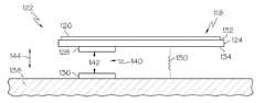
- FIG. 2illustrates an input device 122 , according to one embodiment of the present invention, which may be implemented as the input device 116 shown in FIG. 1 .
- the input device 122 of FIG. 2has been greatly simplified in representation for clarity of explanation. For example, electrical connections, routing lines, discrete components, and other components that may be part of the input device 122 but are not relevant to the current discussion, are not shown.
- the input device 122includes a structural component 124 , a plurality of sensor electrodes 126 (which may be arranged in an array or other pattern, or coupled to a uniform resistive sheet), a capacitive electrode 128 , and a biasing member 130 .
- the structural component 124may be, for example, a flexible or rigid circuit board, a combination of a circuit board with other components such as stiffeners, a metal bracket, a display screen, or any number of other options.
- the structural component 124has first and second substantially opposing sides 132 and 134 .
- the sensor electrodes 126are on the first side 132 of the structural component 124
- the capacitive electrode 128is on the second side 134 of the structural component 124 .
- FIG. 2shows the sensor electrodes 126 and the capacitive electrode 128 being disposed directly on the structural component 124 , it should be understood that this need not be the case.
- the plurality of sensor electrodesmay be indirectly disposed on, or offset from, the structural component 124 , or located on that side of structural component 124 in any number of ways.
- the sensor electrodes 126may be disposed on a circuit assembly that is attached to structural component 124 , or separated from structural component 124 by a gap (e.g., filled with air).
- the capacitive electrode 128may be “on” the second opposing side 134 of the structural component 124 in any number of ways, including being offset from the structural component 124 by a material or vacuum.
- the sensor electrodes 126are configured to capacitively sense positional information associated with user input (e.g., with one or more input objects 114 ) in the sensing region 118 in a manner similar to that described above.
- the capacitive electrode 128may essentially comprise conductive material laid out in a solid patch or other pattern that is configured to capacitively couple with a capacitive electrode 136 that located on a base 138 separated from the capacitive electrode 128 by a gas-filled (e.g., air-filled) gap 140 .
- the base 138may not actually be a base in the sense of being a foundation or support, but the term “base” is used here to describe that it does not move (or moves predictably, repeatably, or relatively little) with the force associated with user input.
- the structural component 124is configured to move with the force associated with user input, and thus and the base 138 and the structural component 124 are configured to be moveable relative to each other with user input force.
- various other electronic and non-electronic componentsmay be part of, or disposed on, the structural component 124 .
- the structural component 124may also include, or be physically coupled to, items such as resistors, inductors, conductive traces electrically interconnecting the various electronic components, metal or polymer pieces, and the like.
- the biasing member 130is configured to be physically coupled to, and positioned between, the second side 134 of the structural component 124 and the base 138 .
- the biasing member 130need not have any particular spring-like response, as long as it is capable of providing biasing force. It should also be understood that, although FIG. 2 shows the biasing member 130 as connected to both structural component 124 and base 138 , the biasing member 130 need not be thus affixed.
- the biasing member 130may be physically attached to the structural component 124 and only touch the base 138 when sufficient input object force(s) is (are) applied.
- the biasing member 130may be physically attached to the structural component 124 and not engage the base 138 until a threshold amount of change in a separation distance 142 between the capacitive electrodes has occurred.
- the biasing membermay be physically attached to base 138 but not the structural component 124 .
- the biasing member 130may be tuned to provide no biasing force until a threshold amount of separation distance 142 has occurred, even if the biasing member 130 is always engaged with both the structural component 124 and the base 138 .
- the biasing member 130may be designed to always provide an amount of biasing force, and bias the structural component 124 against some other component (not shown), such as a bezel or a part of a housing.
- the biasing member 130is configured to regulate the separation distance 142 between the capacitive electrodes 128 and 136 . (Depending on the design of the biasing member 130 , the structural component 124 , and the base 138 , the biasing member 130 may also regulate the distance separating the structural component 124 and the base 138 .) That is, when one or more suitable input objects are in the sensing region 118 and apply a force to the structural component 124 (directly or indirectly—such as via a protective cover over the sensor electrodes 126 and the structural component 124 ), the structural component 124 may move towards the base 138 , as indicated by arrows 144 . With the structure shown in FIG.
- the movement of the structural component 124 towards the base 138causes the capacitive electrode 128 to move relative to capacitive electrode 136 .
- the biasing member 130applies a force to the structural component 124 and the base 138 such that when the one or more input objects are removed from the sensing region 118 , the structural component 124 moves away from the base 138 and effectively returns to its original position.
- This movement of the structural component 124 relative to the base 138causes the separation distance 142 to change.
- the changes in the separation distance 142cause changes in the capacitive coupling between the capacitive electrodes 128 and 136 , as will be appreciated by one skilled in the art.
- an increase in the capacitance between the first and second capacitive electrodes 128 and 136is indicative of a reduction in the separation distance 142 , and thus, an increase in the force applied (i.e., directly or indirectly applied) to the structural component 124 by the one or more input objects, and vice versa.
- either of the capacitive electrodes 128 and 136may be considered to be a “first” capacitive electrode, and the other may be considered a “second” capacitive electrode.
- FIG. 2shows an embodiment that may be produced using a single circuit board with two or more layers of conductive materials.
- a substrate or substrate stack-up of the circuit boardmay serve as the structural component 124 .
- One or more layers of the circuit boardmay contain the sensor electrodes 126 , and the capacitive electrode 128 may also be disposed directly onto a side of the circuit board farther away from where input objects are expected to be (i.e., the side farther from the sensing region 118 ).
- Standard printed circuit board materials and processesmay be used, including copper layers, conductive inks, solder masks, and the like.
- stiffeners or brackets of any number and variety of materialsmay be added as appropriate.
- any number and variety of sensor electrodes 126 , structural components 124 , capacitive electrodes 128 and 136 , and bases 138may be used.
- the systemsmay be constructed in which the base 138 moves with the force associated with the user input instead of structural component 124 .
- Such an alternativeis also quite viable, as long as the separation distance 142 may still be regulated such that a same user input force application would result in substantively the same change in separation distance.
- the capacitive electrodes 128 and 136 , and the biasing member 130need not be directly in-line with structural component 124 , and may be located in extensions from the structural component 124 .
- either or both of the capacitive electrodes 128 and 136may be formed as part of existing materials. In such cases, the capacitive electrodes 128 or 136 may be embedded, flush with a surface, or more flush with the surface, than depicted.
- a commercial sensor for incorporation in an electronic systemmay supply capacitive electrode 128 (which moves with user input force in FIG. 2 ) to couple to an existing conductive feature in the electronic system, capacitive electrode 136 (which does not move with user input force in FIG. 2 ) to couple to an existing conductive feature in the electronic system, or both capacitive electrodes 128 and 136 .
- the capacitive electrodes 128 or 136may be physically coupled in any number of ways to the structural component 124 or the base 138 .
- capacitive electrodes 128 or 136may be attached to the structural component 124 or the base 138 by methods involving adhesives, fasteners, clamping forces, and the like.
- capacitive electrodes 128 or 136may even be formed as part of the structural component 124 or the base 138 .
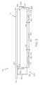
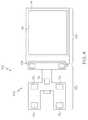
- FIGS. 3 and 4illustrate a touch screen input device 150 , according to an exemplary embodiment of the present invention that operates in a manner similar to the embodiment shown in FIG. 2 .
- the input device 150includes a display screen 152 , a casing 154 , a sensing system 155 , and a protective cover 162 .
- the sensing system 155includes a circuit assembly 156 , capacitive electrodes 176 , and biasing members 158 .
- the capacitive electrodes 176are configured to couple capacitively to one or more capacitive electrodes (not shown) provided, for example, on the casing 154 .
- the display screen 152has first and second sides 164 and 166 (i.e., a “viewing” side 164 that is designed to be viewable to users and a “non-viewing” side 166 that opposes the viewing side in many embodiments).
- the viewing side 164is analogous to the first side 132 and the non-viewing side 166 may be analogous to the second side 134 (if the viewing side and the non-viewing side are opposite each other).
- the display screen 152is a LCD screen with a polarizer 160 , as is commonly understood, although other display technologies are contemplated and may be used.
- the display screen 152is configured to generate one or more images that are visible to a user on, or looking from, the viewing side 164 .
- the polarizer 160 of the LCD-type display screen 152is positioned on the viewing side 164 of the display screen 152 , and is configured to allow only particular polarizations of light to pass therethrough, as is commonly understood. It should be understood that the polarizer 160 is not required for some display screen technologies and, like many other components described here, are optional in embodiments of the present invention.
- the circuit assembly 156in one embodiment, includes a rigid portion 168 and a flexible portion 170 .
- the rigid portion 168includes a substantially transparent substrate that includes an array of sensor electrodes in a sensor electrode area (or simply “sensor electrodes”) 172 , in manner similar to those described above, that define the sensing region 118 .
- the flexible portion 170 of the circuit assembly 156is connected to an edge region 174 of the rigid portion 168 and includes multiple (e.g., four are shown) capacitive electrodes (which may be referred to as “first capacitive electrodes”) 176 formed thereon and an integrated circuit (or controller) 178 mounted thereto.
- the integrated circuit 178may include all or part of the processing system, or processor, which may provide functionality for the sensing system 155 in manner described above.
- FIG. 4shows the circuit assembly 156 in an “unfolded” or “unbent” arrangement (i.e., the circuit assembly is not wrapped around the display screen 152 (not shown in FIG. 4 )).
- sensor electrodes 172 and the capacitive electrodes 176are “facing” substantially the same direction.
- the rigid portion 168 of the circuit assembly 156when installed in the input device 150 , the rigid portion 168 of the circuit assembly 156 is positioned over the polarizer 160 with the sensor electrodes 172 on a side of the rigid portion 168 of the circuit assembly 156 that is facing away from the display screen 152 .
- the sensor electrodes 172 , and the sensing region 118 defined by the sensor electrodes 172at least partially overlap the display screen 152 .
- an image generated by the display screen 152is visible through the sensor electrodes 172 , and thus is overlapped by the sensing region 118 .
- the flexible portion 170 of the circuit assembly 156folds, or bends, around the display screen 152 and is attached to the second side 166 thereof such that the capacitive electrodes 176 face away from the display screen 152 .
- the display screen 152 and the attached portion of the circuit assembly 156are positioned within the casing 154 such that a gap 180 (e.g., filled with a gas such as air) lies between the capacitive electrodes 176 and the capacitive electrodes (not shown) provided on casing 154 .
- the gasalso inhabits the space between the flexible portion 170 of the circuit assembly 156 and the casing 154 .
- a biasing member 158is provided for, and positioned adjacent to, each of the capacitive electrodes 176 . That is, in the embodiment shown in FIGS. 3 and 4 , four biasing members 158 are provided, although only two are explicitly shown in FIG. 3 and none are shown in FIG. 4 .
- the biasing members 158regulate a separation distance 181 associated with the gap 180 when a force is applied to the display screen 152 (e.g., during user input in the sensing region 118 that interacts with a physical part of the input device 150 ).
- the biasing members 158are shaped and their layout configured to provide a monotonic force-displacement response (i.e., have a non-decreasing force-displacement characteristic) to forces that a typical user input would provide.
- Monotonic force-displacement responsesare useful for many types of embodiments, although they are not required.
- Some biasing member designs or layoutsmay include some decreasing force-displacement responses, such as providing a “yielding,” “snapping,” or “clicking” type physical feedback.
- Other embodimentsmay use biasing member(s) to provide strictly monotonic responses (i.e., an always-increasing force-displacement response).
- the shape of the force-displacement response curvemay also be designed as appropriate to the system. For example, some embodiments may use linear or non-linear force-displacement relationships as appropriate.
- biasing membersmay be used.
- the embodiment shown in FIGS. 3 and 4includes four biasing members 158 having substantially dome shapes, laid out at the corners of a rectangle, other arrangements and designs may be found in other embodiments. Any other number of biasing members may be appropriate, including numbers such as one, two, and three. Other shapes may be used, including spherical, cylindrical, spiral, cantilever, leaf-spring-like, combinations thereof, and the like. Also, layout patterns with biasing members in central regions or non-rectilinear layouts may be used.
- the biasing members 158may be made of, for example, elastomeric materials (e.g., rubber), metallic materials, polymeric materials (e.g., plastic), or any combination thereof, and in other embodiments, may be shaped differently (e.g., springs).
- first capacitive electrodes 176are shown laid out in a rectangle in FIGS. 3 and 4 , any number, shapes, and arrangements of first capacitive electrodes 176 may be used.
- At least a portion of the casing 154 that overlaps with the first capacitive electrodes 176is made of a metallic material, such as steel or aluminum. This enables the casing 154 to be used as a second capacitive electrode that capacitively couples with the first capacitive electrodes 176 on the flexible portion 170 of the circuit assembly 156 .
- many casings 154are held at a constant voltage such as ground or driven by known voltage waveforms used to guard the system. In such embodiments, no extra electrodes need to be provided to provide any second capacitive electrodes.
- the second capacitive electrode(s)may be effectively formed on the casing 154 .
- separate second capacitive electrode(s)may be attached (e.g. via adhesive or direct deposition) to a casing made of an electrically insulating material, such as a plastic.
- separate second capacitive electrode(s)may be provided and attached to the casing 154 .
- the integrated circuit 178is adapted to receive indicia from one or more of the capacitive electrodes 176 and thus capacitively sense change in the separation distance 181 between the first capacitive electrodes 176 and the casing (providing the second capacitive electrode(s)) 154 .
- Pushing-type force associated with user input in the sensing region 118causes the sensor system 155 (and generally the display screen 152 ) to move towards the casing 154 .
- the controller or another part of the processing systeme.g., which can be wholly or partially included in the integrated circuit 178 ) may determine the force associated with the user input and applied to the display screen 152 based on the change in the separation distance 181 .
- Some embodimentsmay use multiple sets of capacitive electrodes, each with its own separation distance.
- the systemmay accommodate the multiple separation distance inputs in a variety of ways. For example, the system may use a sum, an average, a maximum, a minimum, one closest to an input object, or some other selection or filtering criterion. Alternatively, the system may estimate the force using any subset or all of the separation distances, and select among the force estimates using a variety of selection, averaging, or filtering methods.
- the controller or another part of the processing systemmay further use positional information associated with the location or velocity of any input objects applying the force in any determinations of the force associated with the user input. This may be especially useful for embodiments in which the change in separation distance varies with the location or direction of the force associated with the user input in the sensing region. In such a case, the system estimates the force using the change in the separation distance and the applicable positional information associated with the user input.
- the systemmay estimate the force using an equation with both changes in separation distance and location (and/or velocity) inputs.
- the systemmay estimate the force by adapting a calculation made with change in separation distance input(s).
- an integrated circuit (or controller), or another part of the processing systemmay be adapted to apply a correction factor or correction amount based on the position of the input object in the sensing region to a calculation based on the separation distance.
- the equation or the correctionmay be obtained through calibration (e.g. by taking many data points of force location and amount to derive an equation that estimates the relationships between the actual force and the change in separation distance), by models of the system response to force (e.g.
- the applied correction factorincreases. In this way, an accurate determination of the applied force may be made even when the force is applied at an area which may have resulted in an inaccurate response without use of the applicable positional information.
- the pushing-type forceis counteracted by the biasing members 158 .
- a decrease in the separation distance 142causes the biasing members 158 to compress and apply an opposing force to the display screen 152 and the casing 154 .
- This opposing forcehelps to return the display screen 152 , the sensor system 155 , and the components connected thereto, to their original positions when the input force is removed from the sensing region 118 .
- one or more input objectsmay still be in the sensing region 118 , but applying no or insignificant force, when these components return to their original positions.
- the integrated circuit 178is also adapted to be in operative communication with the sensor electrodes in sensor electrode area 172 , and sense positional information, as described above, associated with the user input in the sensing region 118 .
- the biasing members 158are designed to carry more than compression force, and are used to help keep the input device components together. However, this may be detrimental to the integrity of the sensor system 155 in some embodiments.
- the biasing members 158are attached to only one of the circuit assembly 156 and the casing 154 such that the biasing members are not stressed if, for example, the display screen 152 experiences a torsion force and is twisted with respect to the casing 154 , or if the display screen 152 experiences a tension force and is pulled away from the casing 154 .
- such forcesmay be applied in cases such as misuse, abuse, accident, or during maintenance.
- the casing 154 shown in FIG. 3also includes tabs 182 that engage, for example, only on the viewing side 164 of the display screen 152 .
- the tabs 182carry the force when torsion or tension twists or pulls the display screen 152 away from the casing 154 , but not when the display screen 152 is moved towards the casing 154 .
- similar or other featuresmay be used to produce such a tension-carrying effect.
- some embodimentsmay be designed such that the biasing members 158 still carry some amount of torsion or tension, while tension-carrying features carry a large part or a predominant portion of the torsion or tension force.
- embodimentsmay include features that carry compression, such that the biasing members 158 carry only part of the compressive force. This may be used to bring the expected compression forces into the range of the sensors, for example.
- FIGS. 5-11illustrate alternative embodiments with respect to various aspects of the present invention.
- FIGS. 5 , 6 , and 7illustrate examples of an input device 200 with alternative embodiments of a circuit assembly 202 which may be similar in some respects to the circuit assembly 156 shown in FIGS. 3 and 4 .
- the input devices 200 of FIGS. 5-7include a structural component (e.g., a display device) 204 arranged in a spaced relationship with a base (e.g., a casing) 206 with a biasing member 207 arranged therebetween, and as such, may operate in a manner similar to the previous mentioned embodiments.
- the rigid portions of circuit assembly 202 discussed belowmay be rigid due to the circuit material (e.g. a thick layer of Flame Retardant 4 (FR4) core) or the use of stiffeners or brackets.
- the flexible portionsmay use flexible substrates such as polyimide, PET, and the like. It is also worth noting that, in the embodiments shown in FIGS.
- capacitive electrodes 220 and 222may be considered the first capacitive electrode, and the other considered the second capacitive electrode. Further, the embodiments shown in FIGS. 5-7 have been greatly simplified for ease of explanation, and any numbers, designs, and layouts of capacitive electrodes, biasing members, and the like may be used.
- the circuit assembly 202includes a first rigid portion 208 , a second rigid portion 210 , and a flexible portion 212 interconnecting the first and second rigid portions 208 and 210 .
- the first rigid portion 208is positioned on a first side 214 of the structural component 204 and has an array of sensor electrodes 216 disposed thereon for sensing positional information associated with user input in sensing region 118 .
- the second rigid portion 210is positioned on a second side 218 of the structural component 204 and has a capacitive electrode 220 disposed thereon.
- the capacitive electrode 220is configured to capacitively couple with a capacitive electrode 222 on the base 206 .
- the rigid portion 210 and associated capacitive electrodemay be disposed on the base 206 instead of structural component 204 , and couple to a capacitive electrode on structural component 204 instead of base 206 .
- the circuit assembly 202includes a first (or a single) rigid portion 208 that has the sensor electrodes 216 disposed thereon.
- the flexible portion 212 of the circuit assembly 202bends around the structural component 204 and is attached to the base 206 .
- the capacitive electrode 220is disposed on the flexible portion 212 of the circuit assembly 202
- the capacitive electrode 222is attached to the second side 218 of the structural component 204 . This may be accomplished, for example, by forming capacitive electrode 222 as part of the structural component 204 .
- an alternative embodimentplaces the flexible portion 212 with the capacitive electrode 220 on the second side 218 of structural component 204 instead of the base 206 .
- capacitive electrode 222is attached to base 206 .
- the circuit assembly 202includes only a flexible portion 212 and does not include any rigid portions.
- a first region 224 of the flexible portion 212is positioned on the first side 214 of the structural component 204 and has the sensor electrodes 216 disposed thereon.
- a second region 226 of the flexible portion 212is positioned on the second side 218 of the structural component 204 and has the first capacitive electrode 220 disposed thereon.
- the flexible portion 212may be instead designed for and attached instead to the base 206 , and the capacitive electrode 222 may be instead attached to the second side 218 .
- circuit assembly 202may contain both capacitive electrodes 220 and 222 .
- FIGS. 8 , 9 , and 10illustrate various arrangements of capacitive electrodes 230 and biasing members 232 with respect to a structural component (and/or a casing) 234 .
- the capacitive electrodes 230 shownmay represent capacitive electrodes on the second side of the display screen (or structural component) or capacitive electrodes on the casing (or base). That is, each capacitive electrode shown in FIGS. 8-10 may represent a pair of capacitive electrodes (i.e., a first capacitive electrode and a second capacitive electrode).
- embodiments of the present inventionmay utilize multiple first capacitive electrodes and/or multiple second capacitive electrodes, as well as multiple biasing members.
- the structural component (and/or a casing) 234may not be in the shape of a rectangle, even though rectangular portions of the structural component (and/or a casing) 234 are shown in FIGS. 8-10 .
- the structural component (and/or a casing) 234is referred to as the structural component 234 below.
- the parts shown of the structural components (and/or a casing) 234are treated as the entirety of the structural components (and/or a casing) 234 , even though it may extend beyond the rectilinear portion shown.
- the capacitive electrode (or the pair of capacitive electrodes) 230is positioned at a central portion of the structural component (and/or the casing) 234 , and the biasing members 232 are positioned near respective corners of the structural component 234 .
- the biasing member 232is positioned at the central portion of the structural component 234 , and the capacitive electrodes 230 are positioned at respective corners of the structural component 234 .
- the embodiment shown in FIG. 10includes three capacitive electrodes (or pairs of capacitive electrodes) 230 in a first triangular pattern and three biasing members 232 in a second triangular pattern intersecting the first.
- two of the capacitive electrodes (or two capacitive electrode sets) 230are positioned near corners of the structural component 234 and a biasing member 232 is positioned therebetween.
- two of the biasing members 232are positioned near corners of the structural component 234 , while one of the capacitive electrodes 230 is positioned therebetween.
- FIG. 11illustrates a portion of a casing 250 according to another embodiment of the present invention. This portion is often considered a “bottom piece” as it is often away from the user input side of any electronic systems it is associated with.
- the casing 250includes, for example, three biasing members 252 that are connected thereto in the form of cantilever springs.
- the biasing members 252are formed as part of the casing (i.e., the biasing members are stamped out or injection molded with the rest of the casing 250 , when the casing 250 was manufactured).
- the biasing members 252may be made of the same material as the casing 250 .
- One advantage of most embodiments of the input devices described aboveis that both the positional information and the force associated with the position information are determined using capacitive sensing. As a result, the overall design of the systems may be simplified, and the number of different parts required reduced. As a result, manufacturing costs are reduced. Additionally, because capacitive sensing is used for both the positional information and associated force, the electronics needed to determine both are simplified, which reduces processing time, improves performance, and further reduces costs over many previous methods of measuring force capacitively.
Landscapes
- Engineering & Computer Science (AREA)
- General Engineering & Computer Science (AREA)
- Theoretical Computer Science (AREA)
- Human Computer Interaction (AREA)
- Physics & Mathematics (AREA)
- General Physics & Mathematics (AREA)
- Position Input By Displaying (AREA)
- Switches That Are Operated By Magnetic Or Electric Fields (AREA)
Abstract
Description
Claims (22)
Priority Applications (3)
| Application Number | Priority Date | Filing Date | Title |
|---|---|---|---|
| US12/418,433US9024907B2 (en) | 2009-04-03 | 2009-04-03 | Input device with capacitive force sensor and method for constructing the same |
| PCT/US2010/029823WO2010115131A2 (en) | 2009-04-03 | 2010-04-02 | Input device with capacitive force sensor and method for constructing the same |
| US14/661,928US9772729B2 (en) | 2009-04-03 | 2015-03-18 | Input device with capacitive force sensor and method for constructing the same |
Applications Claiming Priority (1)
| Application Number | Priority Date | Filing Date | Title |
|---|---|---|---|
| US12/418,433US9024907B2 (en) | 2009-04-03 | 2009-04-03 | Input device with capacitive force sensor and method for constructing the same |
Related Child Applications (1)
| Application Number | Title | Priority Date | Filing Date |
|---|---|---|---|
| US14/661,928ContinuationUS9772729B2 (en) | 2009-04-03 | 2015-03-18 | Input device with capacitive force sensor and method for constructing the same |
Publications (2)
| Publication Number | Publication Date |
|---|---|
| US20100253645A1 US20100253645A1 (en) | 2010-10-07 |
| US9024907B2true US9024907B2 (en) | 2015-05-05 |
Family
ID=42825796
Family Applications (2)
| Application Number | Title | Priority Date | Filing Date |
|---|---|---|---|
| US12/418,433Expired - Fee RelatedUS9024907B2 (en) | 2009-04-03 | 2009-04-03 | Input device with capacitive force sensor and method for constructing the same |
| US14/661,928Active2029-08-22US9772729B2 (en) | 2009-04-03 | 2015-03-18 | Input device with capacitive force sensor and method for constructing the same |
Family Applications After (1)
| Application Number | Title | Priority Date | Filing Date |
|---|---|---|---|
| US14/661,928Active2029-08-22US9772729B2 (en) | 2009-04-03 | 2015-03-18 | Input device with capacitive force sensor and method for constructing the same |
Country Status (2)
| Country | Link |
|---|---|
| US (2) | US9024907B2 (en) |
| WO (1) | WO2010115131A2 (en) |
Cited By (38)
| Publication number | Priority date | Publication date | Assignee | Title |
|---|---|---|---|---|
| US20150138112A1 (en)* | 2013-11-20 | 2015-05-21 | Nextinput, Inc. | Force sensor module for applying a preload force to a force sensor |
| US20150193056A1 (en)* | 2009-04-03 | 2015-07-09 | Synaptics Incorporated | Input device with capacitive force sensor and method for constructing the same |
| US20160209984A1 (en)* | 2013-09-28 | 2016-07-21 | Apple Inc. | Compensation for Nonlinear Variation of Gap Capacitance with Displacement |
| US9671889B1 (en) | 2013-07-25 | 2017-06-06 | Apple Inc. | Input member with capacitive sensor |
| US9715301B2 (en) | 2015-08-04 | 2017-07-25 | Apple Inc. | Proximity edge sensing |
| US9772721B2 (en) | 2012-07-26 | 2017-09-26 | Apple Inc. | Ultrasound-based force sensing and touch sensing |
| US9851828B2 (en) | 2013-03-15 | 2017-12-26 | Apple Inc. | Touch force deflection sensor |
| US9891738B2 (en) | 2012-07-26 | 2018-02-13 | Apple Inc. | Ultrasound-based force sensing of inputs |
| US10007343B2 (en) | 2016-03-31 | 2018-06-26 | Apple Inc. | Force sensor in an input device |
| US10006937B2 (en) | 2015-03-06 | 2018-06-26 | Apple Inc. | Capacitive sensors for electronic devices and methods of forming the same |
| US10048789B2 (en) | 2014-02-12 | 2018-08-14 | Apple Inc. | Force determination employing sheet sensor and capacitive array |
| US10048801B2 (en) | 2016-02-29 | 2018-08-14 | Synaptics Incorporated | Adaptive mechanical change compensation for force detector |
| US10061428B2 (en) | 2016-06-30 | 2018-08-28 | Synaptics Incorporated | Detecting applied forces on a display |
| US10095341B2 (en) | 2016-06-30 | 2018-10-09 | Synaptics Incorporated | Hybrid force measurement |
| US10126861B2 (en) | 2015-05-08 | 2018-11-13 | Synaptics Incorporated | Force sensor substrate |
| US10162444B2 (en) | 2012-12-14 | 2018-12-25 | Apple Inc. | Force sensor incorporated into display |
| US10168814B2 (en) | 2012-12-14 | 2019-01-01 | Apple Inc. | Force sensing based on capacitance changes |
| US10193549B2 (en) | 2015-12-29 | 2019-01-29 | Samsung Electronics Co., Ltd. | Sensing apparatus |
| US10198123B2 (en) | 2014-04-21 | 2019-02-05 | Apple Inc. | Mitigating noise in capacitive sensor |
| US10198133B2 (en) | 2016-03-28 | 2019-02-05 | Synaptics Incorporated | Inflection based calibration method for force detector |
| US10303280B2 (en) | 2016-09-20 | 2019-05-28 | Samsung Display Co., Ltd. | Touch sensor and display device including the same |
| US10372259B2 (en) | 2016-02-19 | 2019-08-06 | Synaptics Incorporated | Transcapacitive touch and force sensing in an input device |
| US10386970B2 (en) | 2013-02-08 | 2019-08-20 | Apple Inc. | Force determination based on capacitive sensing |
| US10394393B2 (en) | 2015-10-09 | 2019-08-27 | Synaptics Incorporated | Compensating force baseline artifacts in a capacitive sensor |
| US10444862B2 (en) | 2014-08-22 | 2019-10-15 | Synaptics Incorporated | Low-profile capacitive pointing stick |
| US10452211B2 (en) | 2016-05-27 | 2019-10-22 | Synaptics Incorporated | Force sensor with uniform response in an axis |
| US10593737B2 (en) | 2016-11-02 | 2020-03-17 | Samsung Display Co., Ltd. | Display device |
| US10591368B2 (en) | 2014-01-13 | 2020-03-17 | Apple Inc. | Force sensor with strain relief |
| US10642361B2 (en) | 2012-06-12 | 2020-05-05 | Apple Inc. | Haptic electromagnetic actuator |
| US10733408B2 (en) | 2016-09-23 | 2020-08-04 | Samsung Display Co., Ltd. | Display device |
| US10770517B2 (en) | 2016-09-08 | 2020-09-08 | Samsung Display Co., Ltd. | Foldable display device |
| US10866683B2 (en) | 2018-08-27 | 2020-12-15 | Apple Inc. | Force or touch sensing on a mobile device using capacitive or pressure sensing |
| US10921943B2 (en) | 2019-04-30 | 2021-02-16 | Apple Inc. | Compliant material for protecting capacitive force sensors and increasing capacitive sensitivity |
| US20210055810A1 (en)* | 2018-05-18 | 2021-02-25 | Alps Alpine Co., Ltd. | Input device |
| US10949020B2 (en) | 2012-07-26 | 2021-03-16 | Apple Inc. | Fingerprint-assisted force estimation |
| US11048370B2 (en) | 2016-12-29 | 2021-06-29 | Samsung Display Co., Ltd. | Display device and method of manufacturing the same |
| US11227898B2 (en) | 2016-07-26 | 2022-01-18 | Samsung Display Co., Ltd. | Display apparatus |
| US11592946B1 (en) | 2021-09-21 | 2023-02-28 | Apple Inc. | Capacitive gap force sensor with multi-layer fill |
Families Citing this family (82)
| Publication number | Priority date | Publication date | Assignee | Title |
|---|---|---|---|---|
| TW200842681A (en) | 2007-04-27 | 2008-11-01 | Tpk Touch Solutions Inc | Touch pattern structure of a capacitive touch panel |
| US9654104B2 (en)* | 2007-07-17 | 2017-05-16 | Apple Inc. | Resistive force sensor with capacitive discrimination |
| US8605050B2 (en) | 2007-08-21 | 2013-12-10 | Tpk Touch Solutions (Xiamen) Inc. | Conductor pattern structure of capacitive touch panel |
| TWI374379B (en) | 2007-12-24 | 2012-10-11 | Wintek Corp | Transparent capacitive touch panel and manufacturing method thereof |
| WO2010105507A1 (en) | 2009-03-20 | 2010-09-23 | 宸鸿科技(厦门)有限公司 | Capacitive touch circuit pattern and manufacturing method thereof |
| JP5548270B2 (en)* | 2009-08-21 | 2014-07-16 | アップル インコーポレイテッド | Capacitive sensing method and apparatus |
| US10068728B2 (en)* | 2009-10-15 | 2018-09-04 | Synaptics Incorporated | Touchpad with capacitive force sensing |
| US8570297B2 (en)* | 2009-12-14 | 2013-10-29 | Synaptics Incorporated | System and method for measuring individual force in multi-object sensing |
| US8587422B2 (en) | 2010-03-31 | 2013-11-19 | Tk Holdings, Inc. | Occupant sensing system |
| DE102011006448A1 (en) | 2010-03-31 | 2011-10-06 | Tk Holdings, Inc. | steering wheel sensors |
| DE102011006649B4 (en) | 2010-04-02 | 2018-05-03 | Tk Holdings Inc. | Steering wheel with hand sensors |
| WO2012012299A2 (en)* | 2010-07-21 | 2012-01-26 | Synaptics Incorporated | Producing capacitive images comprising non-connection values |
| GB2488600B (en)* | 2011-03-04 | 2013-05-29 | Hm Technology Internat Ltd | A force sensor |
| CN102866794A (en) | 2011-06-15 | 2013-01-09 | 宸鸿光电科技股份有限公司 | Touch sensing layer and manufacturing method thereof |
| US20130018489A1 (en)* | 2011-07-14 | 2013-01-17 | Grunthaner Martin Paul | Combined force and proximity sensing |
| WO2013107474A1 (en)* | 2012-01-20 | 2013-07-25 | Sony Ericsson Mobile Communications Ab | Touch screen, portable electronic device, and method of operating a touch screen |
| US20130257792A1 (en)* | 2012-04-02 | 2013-10-03 | Synaptics Incorporated | Systems and methods for determining user input using position information and force sensing |
| WO2013154720A1 (en) | 2012-04-13 | 2013-10-17 | Tk Holdings Inc. | Pressure sensor including a pressure sensitive material for use with control systems and methods of using the same |
| WO2013170099A1 (en)* | 2012-05-09 | 2013-11-14 | Yknots Industries Llc | Calibration of haptic feedback systems for input devices |
| WO2013177322A1 (en)* | 2012-05-22 | 2013-11-28 | Synaptics Incorporated | Force enhanced input device |
| DE102012213020A1 (en) | 2012-07-25 | 2014-05-22 | Bayerische Motoren Werke Aktiengesellschaft | Input device with retractable touch-sensitive surface |
| US9182859B2 (en)* | 2012-08-29 | 2015-11-10 | Sharp Kabushiki Kaisha | Capacitive touch panel with force sensing |
| WO2014035479A2 (en)* | 2012-08-30 | 2014-03-06 | Changello Enterprise Llc | Auto-baseline determination for force sensing |
| CN104662496B (en)* | 2012-09-11 | 2017-07-07 | 平蛙实验室股份公司 | Touch Force Estimation in FTIR-Based Projection-Type Touch Sensing Devices |
| WO2014043664A1 (en) | 2012-09-17 | 2014-03-20 | Tk Holdings Inc. | Single layer force sensor |
| KR101681305B1 (en)* | 2014-08-01 | 2016-12-02 | 주식회사 하이딥 | Touch input device |
| KR101452302B1 (en) | 2013-07-29 | 2014-10-22 | 주식회사 하이딥 | Touch sensor panel |
| KR101712346B1 (en) | 2014-09-19 | 2017-03-22 | 주식회사 하이딥 | Touch input device |
| JP6527343B2 (en) | 2014-08-01 | 2019-06-05 | 株式会社 ハイディープHiDeep Inc. | Touch input device |
| JP5845371B1 (en)* | 2014-09-19 | 2016-01-20 | 株式会社 ハイディープ | smartphone |
| DE102014016772A1 (en) | 2014-11-13 | 2016-05-19 | Audi Ag | Input device for a motor vehicle, motor vehicle with an input device and method for operating an input device |
| EP3457263A1 (en) | 2014-12-23 | 2019-03-20 | Cambridge Touch Technologies, Ltd. | Pressure-sensitive touch panel |
| GB2533667B (en) | 2014-12-23 | 2017-07-19 | Cambridge Touch Tech Ltd | Pressure-sensitive touch panel |
| KR101577277B1 (en)* | 2015-02-04 | 2015-12-28 | 주식회사 하이딥 | Touch type distinguishing method and touch input device performing the same |
| KR101652029B1 (en)* | 2015-04-13 | 2016-08-30 | 주식회사 하이딥 | Pressure detection module and smartphone including the same |
| KR101583221B1 (en)* | 2015-06-17 | 2016-01-07 | 주식회사 하이딥 | Electrode sheet for pressure detection and pressure detecting module including the same |
| TWI587189B (en)* | 2015-07-17 | 2017-06-11 | 林志忠 | Touch panel with pressure sensing function |
| KR20170020725A (en)* | 2015-07-29 | 2017-02-24 | 주식회사 하이딥 | Touch input device including display module formed with pressure sensing electrode and pressure sensing electrode forming method |
| CN107077017B (en)* | 2015-08-25 | 2021-08-03 | 华为技术有限公司 | a terminal |
| JP6625372B2 (en)* | 2015-08-27 | 2019-12-25 | 株式会社デンソーテン | Input device and in-vehicle device |
| US9857928B2 (en) | 2015-09-08 | 2018-01-02 | Microsoft Technology Licensing, Llc | Force sensitive device |
| US9652069B1 (en) | 2015-10-22 | 2017-05-16 | Synaptics Incorporated | Press hard and move gesture |
| CN105446538B (en) | 2015-10-29 | 2017-07-21 | 深圳市汇顶科技股份有限公司 | A kind of pressure detection structure and touch apparatus |
| WO2017083533A1 (en)* | 2015-11-12 | 2017-05-18 | Synaptics Incorporated | Determining thickness profiles for dielectric layer within input device |
| US20170153760A1 (en)* | 2015-12-01 | 2017-06-01 | Apple Inc. | Gain-based error tracking for force sensing |
| US10254870B2 (en) | 2015-12-01 | 2019-04-09 | Apple Inc. | Force sensor-based motion or orientation determination in a device |
| CN106855759A (en)* | 2015-12-16 | 2017-06-16 | 小米科技有限责任公司 | Touch controlled key, contact panel and touch control terminal |
| US10282046B2 (en) | 2015-12-23 | 2019-05-07 | Cambridge Touch Technologies Ltd. | Pressure-sensitive touch panel |
| GB2544353B (en) | 2015-12-23 | 2018-02-21 | Cambridge Touch Tech Ltd | Pressure-sensitive touch panel |
| CN106909244B (en)* | 2015-12-31 | 2020-01-10 | 小米科技有限责任公司 | Touch key, touch operation detection method, touch IC and electronic equipment |
| CN105607775A (en) | 2016-01-18 | 2016-05-25 | 京东方科技集团股份有限公司 | Pressure touch display device and pressure touch method |
| US11064768B2 (en) | 2016-03-15 | 2021-07-20 | Nike, Inc. | Foot presence signal processing using velocity |
| US11357290B2 (en) | 2016-03-15 | 2022-06-14 | Nike, Inc. | Active footwear sensor calibration |
| US11026481B2 (en) | 2016-03-15 | 2021-06-08 | Nike, Inc. | Foot presence signal processing using velocity |
| KR102494900B1 (en) | 2016-03-15 | 2023-02-01 | 나이키 이노베이트 씨.브이. | Capacitive Foot Presence Detection for Footwear |
| KR101811414B1 (en)* | 2016-03-16 | 2017-12-21 | 주식회사 하이딥 | Touch input depvice |
| US10088942B2 (en) | 2016-03-31 | 2018-10-02 | Synaptics Incorporated | Per-finger force detection using segmented sensor electrodes |
| KR102532769B1 (en)* | 2016-06-10 | 2023-05-17 | 삼성디스플레이 주식회사 | Display device |
| JP6739556B2 (en) | 2016-06-30 | 2020-08-12 | コーニンクレッカ フィリップス エヌ ヴェKoninklijke Philips N.V. | Sealed control panel for medical devices |
| US10540027B2 (en)* | 2016-06-30 | 2020-01-21 | Synaptics Incorporated | Force sensing in a touch display |
| US11449214B2 (en)* | 2016-08-25 | 2022-09-20 | Parade Technologies, Ltd. | 3D touch enabled gestures |
| US10528088B2 (en)* | 2016-09-28 | 2020-01-07 | Microsoft Technology Licensing, Llc | Opening state detection of a foldable device using self-capacitance |
| EP3549001A4 (en)* | 2016-12-02 | 2020-05-27 | Methode Electronics, Inc. | Integrated control panel apparatus and use thereof |
| US10209796B2 (en)* | 2017-02-03 | 2019-02-19 | Google Llc | Display assembly connector device |
| CN110300950B (en) | 2017-02-06 | 2023-06-16 | 平蛙实验室股份公司 | Optical coupling in touch sensing systems |
| CN108734097B (en)* | 2017-04-14 | 2024-04-02 | 辛纳普蒂克斯公司 | Integrated fingerprint and force sensor |
| US10379672B2 (en) | 2017-07-13 | 2019-08-13 | Synaptics Incorporated | Dynamic proximity object detection |
| US11093088B2 (en) | 2017-08-08 | 2021-08-17 | Cambridge Touch Technologies Ltd. | Device for processing signals from a pressure-sensing touch panel |
| GB2565305A (en) | 2017-08-08 | 2019-02-13 | Cambridge Touch Tech Ltd | Device for processing signals from a pressure-sensing touch panel |
| US11256371B2 (en) | 2017-09-01 | 2022-02-22 | Flatfrog Laboratories Ab | Optical component |
| GB2568543B (en) | 2017-11-21 | 2020-12-09 | Johnson Electric Int Ag | Multi-stage capacitive sensor |
| US10831320B2 (en)* | 2017-11-30 | 2020-11-10 | Synaptics Incorporated | Self-referenced capacitive force sensor |
| DE102017223731A1 (en)* | 2017-12-22 | 2019-06-27 | Continental Automotive Gmbh | Electro-optical touchscreen with integrated pressure sensing |
| US10635248B2 (en)* | 2018-01-05 | 2020-04-28 | Amtel Corporation | Force sensor mount and related housings and systems that incorporate the same |
| US10459542B1 (en)* | 2018-06-01 | 2019-10-29 | Google Llc | Trackpad with capacitive force sensing and haptic feedback |
| US10642428B2 (en)* | 2018-06-25 | 2020-05-05 | Synpatics Incorporated | Engineering displacement response through electrode shape |
| WO2020080992A1 (en) | 2018-10-20 | 2020-04-23 | Flatfrog Laboratories Ab | Frame for a touch-sensitive device and tool therefor |
| DE102019105285A1 (en)* | 2019-03-01 | 2020-09-03 | Motherson Innovations Company Limited | Operating component for a device with a hidden-to-lit pattern |
| ES2991658T3 (en) | 2019-11-25 | 2024-12-04 | Flatfrog Lab Ab | A touch device |
| US12282653B2 (en) | 2020-02-08 | 2025-04-22 | Flatfrog Laboratories Ab | Touch apparatus with low latency interactions |
| JP7235003B2 (en)* | 2020-05-19 | 2023-03-08 | 株式会社デンソー | Vehicle operating device |
| CN111982161A (en)* | 2020-07-30 | 2020-11-24 | 拉扎斯网络科技(上海)有限公司 | Method and device for determining orientation of conductor object |
Citations (80)
| Publication number | Priority date | Publication date | Assignee | Title |
|---|---|---|---|---|
| US4290052A (en)* | 1979-10-26 | 1981-09-15 | General Electric Company | Capacitive touch entry apparatus having high degree of personal safety |
| US4719538A (en) | 1986-12-02 | 1988-01-12 | Cox John D | Force responsive capacitive transducer |
| JPH07280671A (en) | 1994-04-07 | 1995-10-27 | Nitta Ind Corp | Electrostatic capacity type force sensor |
| US5492020A (en) | 1991-03-30 | 1996-02-20 | Okada; Kazuhiro | Detector for a physical quantity having a self-testing function |
| US5510813A (en) | 1993-08-26 | 1996-04-23 | U.S. Philips Corporation | Data processing device comprising a touch screen and a force sensor |
| WO1997018528A1 (en) | 1995-11-13 | 1997-05-22 | Synaptics, Inc. | Stylus input capacitive touchpad sensor |
| US5854625A (en) | 1996-11-06 | 1998-12-29 | Synaptics, Incorporated | Force sensing touchpad |
| US5942733A (en) | 1992-06-08 | 1999-08-24 | Synaptics, Inc. | Stylus input capacitive touchpad sensor |
| US5945980A (en) | 1997-11-14 | 1999-08-31 | Logitech, Inc. | Touchpad with active plane for pen detection |
| US5973668A (en) | 1995-07-21 | 1999-10-26 | Oki Electric Industry Co., Ltd. | Pointing device |
| US6002389A (en) | 1996-04-24 | 1999-12-14 | Logitech, Inc. | Touch and pressure sensing method and apparatus |
| US6215476B1 (en) | 1997-10-10 | 2001-04-10 | Apple Computer, Inc. | Flat panel display with integrated electromagnetic pen digitizer |
| US20020019711A1 (en) | 2000-03-07 | 2002-02-14 | Haruzo Miyashita | Anticorrosive vacuum sensor |
| US20020180710A1 (en) | 2001-04-13 | 2002-12-05 | Roberts Jerry B. | Force sensors and touch panels using same |
| US20030151589A1 (en) | 2002-02-13 | 2003-08-14 | Siemens Technology-To-Business Center, Llc | Configurable industrial input devices that use electrically conductive elastomer |
| US6642857B1 (en) | 2000-01-19 | 2003-11-04 | Synaptics Incorporated | Capacitive pointing stick |
| US20040112149A1 (en) | 2000-12-14 | 2004-06-17 | Gebert Rudiger Heinz | Weight sensor |
| US20040155991A1 (en) | 2002-11-21 | 2004-08-12 | Lowles Robert J. | System and method of integrating a touchscreen within an LCD |
| US20040227736A1 (en) | 2003-05-16 | 2004-11-18 | Kamrath Robert F. | Capacitor based force sensor |
| US20050052425A1 (en) | 2003-08-18 | 2005-03-10 | Zadesky Stephen Paul | Movable touch pad with added functionality |
| US20050057528A1 (en) | 2003-09-01 | 2005-03-17 | Martin Kleen | Screen having a touch-sensitive user interface for command input |
| US20050057266A1 (en) | 2002-05-29 | 2005-03-17 | Hideo Morimoto | Capacitance type sensor and method for manufacturing same |
| US20050061082A1 (en) | 2003-04-09 | 2005-03-24 | Dallenbach Willaim David | Capacitive force sensing device |
| WO2005121729A1 (en) | 2004-06-09 | 2005-12-22 | Eth Zürich Eth Transfer | Textile capacitive pressure sensor |
| US20060017701A1 (en) | 2002-10-28 | 2006-01-26 | Victor Marten | Data acquistion from capacitive touch pad |
| US20060197753A1 (en) | 2005-03-04 | 2006-09-07 | Hotelling Steven P | Multi-functional hand-held device |
| US20070063982A1 (en) | 2005-09-19 | 2007-03-22 | Tran Bao Q | Integrated rendering of sound and image on a display |
| WO2007098171A2 (en) | 2006-02-21 | 2007-08-30 | Cirque Corporation | System for providing tactile sensation to a robotic grasping mechanism using capacitance touchpad technology |
| US20070229464A1 (en)* | 2006-03-30 | 2007-10-04 | Apple Computer, Inc. | Force Imaging Input Device and System |
| US20070229470A1 (en) | 2006-03-31 | 2007-10-04 | Warren Snyder | Capacitive touch sense device having polygonal shaped sensor elements |
| US20070236450A1 (en) | 2006-03-24 | 2007-10-11 | Northwestern University | Haptic device with indirect haptic feedback |
| US20070257821A1 (en) | 2006-04-20 | 2007-11-08 | Son Jae S | Reconfigurable tactile sensor input device |
| US20070268265A1 (en) | 2006-05-18 | 2007-11-22 | Cypress Semiconductor Corporation | Two-pin buttons |
| US20080018611A1 (en)* | 2006-07-18 | 2008-01-24 | Iee International Electronics & Engineering S.A. | Input Device |
| US20080062148A1 (en)* | 2006-06-09 | 2008-03-13 | Hotelling Steve P | Touch screen liquid crystal display |
| US20080068348A1 (en) | 1998-06-23 | 2008-03-20 | Immersion Corporation | Haptic feedback for touchpads and other touch controls |
| US20080142352A1 (en) | 2006-12-18 | 2008-06-19 | Wright David G | Two circuit board touch-sensor device |
| US20080190210A1 (en) | 2007-02-12 | 2008-08-14 | Loadstar Sensors, Inc. | Capacitive device and method with an enhanced measurement error correction capability |
| US20080202251A1 (en)* | 2007-02-27 | 2008-08-28 | Iee International Electronics & Engineering S.A. | Capacitive pressure sensor |
| US20080202824A1 (en) | 2007-02-13 | 2008-08-28 | Harald Philipp | Tilting Touch Control Panel |
| US7451659B2 (en) | 2004-09-29 | 2008-11-18 | Loadstar Sensors, Inc. | Gap-change sensing through capacitive techniques |
| US20090002328A1 (en) | 2007-06-26 | 2009-01-01 | Immersion Corporation, A Delaware Corporation | Method and apparatus for multi-touch tactile touch panel actuator mechanisms |
| JP2009009249A (en) | 2007-06-26 | 2009-01-15 | Nissha Printing Co Ltd | Capacitance type touch panel and two system combined use touch panel using the same |
| US20090160763A1 (en) | 2007-12-21 | 2009-06-25 | Patrick Cauwels | Haptic Response Apparatus for an Electronic Device |
| US20090160682A1 (en) | 2003-08-05 | 2009-06-25 | Bolender Robert J | Capacitive sensing device for use in a keypad assembly |
| US20090167704A1 (en) | 2007-12-31 | 2009-07-02 | Apple Inc. | Multi-touch display screen with localized tactile feedback |
| US20090244017A1 (en) | 2008-03-28 | 2009-10-01 | Denso International America, Inc. | Haptic tracking remote control for driver information center system |
| US20090243817A1 (en) | 2008-03-30 | 2009-10-01 | Pressure Profile Systems Corporation | Tactile Device with Force Sensitive Touch Input Surface |
| US20090267892A1 (en) | 2008-04-24 | 2009-10-29 | Research In Motion Limited | System and method for generating energy from activation of an input device in an electronic device |
| WO2009157614A1 (en) | 2008-06-24 | 2009-12-30 | Korea Research Institute Of Standards And Science | Touch inputting apparatus integral sensors and method for acquiring location and intensity of force |
| US20100018889A1 (en) | 2008-07-22 | 2010-01-28 | Graham Packaging Company, L.P. | Stackable Flexible Container Assembly |
| US20100020039A1 (en) | 2005-10-17 | 2010-01-28 | Industrial Technology Research Institute | Touch input device with display front |
| US7656465B2 (en) | 2001-09-07 | 2010-02-02 | Sharp Kabushiki Kaisha | Liquid crystal display and method of manufacturing the same |
| US20100024573A1 (en) | 2008-07-29 | 2010-02-04 | Dodge Daverman | Single Sided Capacitive Force Sensor for Electronic Devices |
| US20100026664A1 (en) | 2008-08-01 | 2010-02-04 | Geaghan Bernard O | Touch sensitive devices with composite electrodes |
| US20100033354A1 (en) | 2006-12-15 | 2010-02-11 | Bang & Olufsen A/S | Touch sensitive device |
| WO2010018889A1 (en) | 2008-08-11 | 2010-02-18 | Korea Research Institute Of Standards And Science | Structure of touch input for acquiring location and intensity of force, apparatus therewith and acquiring method thereof |
| US20100079384A1 (en) | 2008-09-26 | 2010-04-01 | Cypress Semiconductor Corporation | Capacitance touch screen |
| US20100090813A1 (en) | 2008-10-10 | 2010-04-15 | Richard Je | Electronic Device with Localized Haptic Response |
| US20100108409A1 (en) | 2008-11-06 | 2010-05-06 | Jun Tanaka | Capacitive coupling type touch panel |
| US7728487B2 (en) | 2006-03-03 | 2010-06-01 | Olympus Medical Systems Corp. | Ultrasound transducer manufactured by using micromachining process, its device, endoscopic ultrasound diagnosis system thereof, and method for controlling the same |
| US20100149128A1 (en) | 2008-12-11 | 2010-06-17 | No Sang-Yong | Liquid crystal display panel having integrated pressure sending units |
| US20100156814A1 (en) | 2008-12-23 | 2010-06-24 | Research In Motion Limited | Portable electronic device including tactile touch-sensitive input device and method of controlling same |
| US7786655B2 (en) | 2002-09-27 | 2010-08-31 | Innochips Technology | Piezoelectric vibrator with internal electrodes |
| US20100244628A1 (en) | 2009-03-30 | 2010-09-30 | Kabushiki Kaisha Toshiba | Piezoelectric-driven mems element |
| US20100250071A1 (en) | 2008-03-28 | 2010-09-30 | Denso International America, Inc. | Dual function touch switch with haptic feedback |
| US20110005845A1 (en) | 2009-07-07 | 2011-01-13 | Apple Inc. | Touch sensing device having conductive nodes |
| US20110025631A1 (en) | 2008-04-02 | 2011-02-03 | Han Sang-Youl | Capacitive touch screen |
| US7903091B2 (en) | 2005-08-30 | 2011-03-08 | Samsung Electronics Co., Ltd. | Touch panel having a speaker function |
| US20110148811A1 (en) | 2009-12-22 | 2011-06-23 | Sony Corporation | Sensor apparatus and information processing apparatus |
| US20110148812A1 (en) | 2008-09-08 | 2011-06-23 | Koninklijke Philips Electronics N.V. | Oled device with capacitive proximity sensing means |
| US20110175844A1 (en) | 2010-01-19 | 2011-07-21 | Sony Ericsson Mobile Communications Ab | Touch sensing device, touch screen device comprising the touch sensing device, mobile device, method for sensing a touch and method for manufacturing a touch sensing device |
| US20110278078A1 (en) | 2010-05-11 | 2011-11-17 | Synaptics Incorporated | Input device with force sensing |
| US8120229B2 (en) | 2005-05-18 | 2012-02-21 | Kolo Technologies, Inc. | Middle spring supported micro-electro-mechanical transducers |
| US20120075243A1 (en) | 2010-09-24 | 2012-03-29 | Koji Doi | Display Device |
| US20120090902A1 (en) | 2010-10-13 | 2012-04-19 | Sunrex Technology Corp. | Touch pad |
| US20120098783A1 (en) | 2010-10-12 | 2012-04-26 | Cypress Semiconductor Corporation | Flexible Capacitive Sensor Array |
| US20120105333A1 (en) | 2010-11-02 | 2012-05-03 | Apple Inc. | Methods and systems for providing haptic control |
| US20120242610A1 (en) | 2009-11-20 | 2012-09-27 | Sharp Kabushiki Kaisha | Flexible display panel with touch sensor function |
| US8698769B2 (en) | 2011-08-01 | 2014-04-15 | Sharp Kabushiki Kaisha | Dual mode capacitive touch panel |
Family Cites Families (3)
| Publication number | Priority date | Publication date | Assignee | Title |
|---|---|---|---|---|
| US6125476A (en)* | 1999-01-07 | 2000-10-03 | Jerome; Sandra A. | Male undergarment |
| KR101305071B1 (en)* | 2007-01-22 | 2013-09-11 | 삼성디스플레이 주식회사 | Array substrate and display panel having the same |
| US9024907B2 (en)* | 2009-04-03 | 2015-05-05 | Synaptics Incorporated | Input device with capacitive force sensor and method for constructing the same |
- 2009
- 2009-04-03USUS12/418,433patent/US9024907B2/ennot_activeExpired - Fee Related
- 2010
- 2010-04-02WOPCT/US2010/029823patent/WO2010115131A2/enactiveApplication Filing
- 2015
- 2015-03-18USUS14/661,928patent/US9772729B2/enactiveActive
Patent Citations (93)
| Publication number | Priority date | Publication date | Assignee | Title |
|---|---|---|---|---|
| US4290052A (en)* | 1979-10-26 | 1981-09-15 | General Electric Company | Capacitive touch entry apparatus having high degree of personal safety |
| US4719538A (en) | 1986-12-02 | 1988-01-12 | Cox John D | Force responsive capacitive transducer |
| US5492020A (en) | 1991-03-30 | 1996-02-20 | Okada; Kazuhiro | Detector for a physical quantity having a self-testing function |
| US5942733A (en) | 1992-06-08 | 1999-08-24 | Synaptics, Inc. | Stylus input capacitive touchpad sensor |
| US5510813A (en) | 1993-08-26 | 1996-04-23 | U.S. Philips Corporation | Data processing device comprising a touch screen and a force sensor |
| JPH07280671A (en) | 1994-04-07 | 1995-10-27 | Nitta Ind Corp | Electrostatic capacity type force sensor |
| US5973668A (en) | 1995-07-21 | 1999-10-26 | Oki Electric Industry Co., Ltd. | Pointing device |
| WO1997018528A1 (en) | 1995-11-13 | 1997-05-22 | Synaptics, Inc. | Stylus input capacitive touchpad sensor |
| US6002389A (en) | 1996-04-24 | 1999-12-14 | Logitech, Inc. | Touch and pressure sensing method and apparatus |
| US5854625A (en) | 1996-11-06 | 1998-12-29 | Synaptics, Incorporated | Force sensing touchpad |
| US6215476B1 (en) | 1997-10-10 | 2001-04-10 | Apple Computer, Inc. | Flat panel display with integrated electromagnetic pen digitizer |
| US5945980A (en) | 1997-11-14 | 1999-08-31 | Logitech, Inc. | Touchpad with active plane for pen detection |
| US20080068348A1 (en) | 1998-06-23 | 2008-03-20 | Immersion Corporation | Haptic feedback for touchpads and other touch controls |
| US6642857B1 (en) | 2000-01-19 | 2003-11-04 | Synaptics Incorporated | Capacitive pointing stick |
| US20020019711A1 (en) | 2000-03-07 | 2002-02-14 | Haruzo Miyashita | Anticorrosive vacuum sensor |
| US20040112149A1 (en) | 2000-12-14 | 2004-06-17 | Gebert Rudiger Heinz | Weight sensor |
| US20020180710A1 (en) | 2001-04-13 | 2002-12-05 | Roberts Jerry B. | Force sensors and touch panels using same |
| US7196694B2 (en) | 2001-04-13 | 2007-03-27 | 3M Innovative Properties Company | Force sensors and touch panels using same |
| US7656465B2 (en) | 2001-09-07 | 2010-02-02 | Sharp Kabushiki Kaisha | Liquid crystal display and method of manufacturing the same |
| US20030151589A1 (en) | 2002-02-13 | 2003-08-14 | Siemens Technology-To-Business Center, Llc | Configurable industrial input devices that use electrically conductive elastomer |
| US6888537B2 (en) | 2002-02-13 | 2005-05-03 | Siemens Technology-To-Business Center, Llc | Configurable industrial input devices that use electrically conductive elastomer |
| US20050057266A1 (en) | 2002-05-29 | 2005-03-17 | Hideo Morimoto | Capacitance type sensor and method for manufacturing same |
| US6958614B2 (en) | 2002-05-29 | 2005-10-25 | Nitta Corporation | Capacitance type sensor and method for manufacturing same |
| US7398587B2 (en) | 2002-05-29 | 2008-07-15 | Nitta Corporation | Method for manufacturing a capacitance type sensor with a movable electrode |
| US7786655B2 (en) | 2002-09-27 | 2010-08-31 | Innochips Technology | Piezoelectric vibrator with internal electrodes |
| US20060017701A1 (en) | 2002-10-28 | 2006-01-26 | Victor Marten | Data acquistion from capacitive touch pad |
| US20040155991A1 (en) | 2002-11-21 | 2004-08-12 | Lowles Robert J. | System and method of integrating a touchscreen within an LCD |
| US20050061082A1 (en) | 2003-04-09 | 2005-03-24 | Dallenbach Willaim David | Capacitive force sensing device |
| US7047818B2 (en) | 2003-04-09 | 2006-05-23 | Loadstar Sensors, Inc. | Capacitive force sensing device |
| US7148882B2 (en) | 2003-05-16 | 2006-12-12 | 3M Innovatie Properties Company | Capacitor based force sensor |
| US20040227736A1 (en) | 2003-05-16 | 2004-11-18 | Kamrath Robert F. | Capacitor based force sensor |
| US20090160682A1 (en) | 2003-08-05 | 2009-06-25 | Bolender Robert J | Capacitive sensing device for use in a keypad assembly |
| US7499040B2 (en) | 2003-08-18 | 2009-03-03 | Apple Inc. | Movable touch pad with added functionality |
| US20050052425A1 (en) | 2003-08-18 | 2005-03-10 | Zadesky Stephen Paul | Movable touch pad with added functionality |
| US20050057528A1 (en) | 2003-09-01 | 2005-03-17 | Martin Kleen | Screen having a touch-sensitive user interface for command input |
| WO2005121729A1 (en) | 2004-06-09 | 2005-12-22 | Eth Zürich Eth Transfer | Textile capacitive pressure sensor |
| US7451659B2 (en) | 2004-09-29 | 2008-11-18 | Loadstar Sensors, Inc. | Gap-change sensing through capacitive techniques |
| US20060197753A1 (en) | 2005-03-04 | 2006-09-07 | Hotelling Steven P | Multi-functional hand-held device |
| US8120229B2 (en) | 2005-05-18 | 2012-02-21 | Kolo Technologies, Inc. | Middle spring supported micro-electro-mechanical transducers |
| US7903091B2 (en) | 2005-08-30 | 2011-03-08 | Samsung Electronics Co., Ltd. | Touch panel having a speaker function |
| US20070063982A1 (en) | 2005-09-19 | 2007-03-22 | Tran Bao Q | Integrated rendering of sound and image on a display |
| US20100020039A1 (en) | 2005-10-17 | 2010-01-28 | Industrial Technology Research Institute | Touch input device with display front |
| WO2007098171A3 (en) | 2006-02-21 | 2008-04-24 | Cirque Corp | System for providing tactile sensation to a robotic grasping mechanism using capacitance touchpad technology |
| WO2007098171A2 (en) | 2006-02-21 | 2007-08-30 | Cirque Corporation | System for providing tactile sensation to a robotic grasping mechanism using capacitance touchpad technology |
| US7728487B2 (en) | 2006-03-03 | 2010-06-01 | Olympus Medical Systems Corp. | Ultrasound transducer manufactured by using micromachining process, its device, endoscopic ultrasound diagnosis system thereof, and method for controlling the same |
| US20070236450A1 (en) | 2006-03-24 | 2007-10-11 | Northwestern University | Haptic device with indirect haptic feedback |
| US20070229464A1 (en)* | 2006-03-30 | 2007-10-04 | Apple Computer, Inc. | Force Imaging Input Device and System |
| US20070229470A1 (en) | 2006-03-31 | 2007-10-04 | Warren Snyder | Capacitive touch sense device having polygonal shaped sensor elements |
| US20070257821A1 (en) | 2006-04-20 | 2007-11-08 | Son Jae S | Reconfigurable tactile sensor input device |
| US20070268265A1 (en) | 2006-05-18 | 2007-11-22 | Cypress Semiconductor Corporation | Two-pin buttons |
| US20080062148A1 (en)* | 2006-06-09 | 2008-03-13 | Hotelling Steve P | Touch screen liquid crystal display |
| US20080018608A1 (en) | 2006-07-18 | 2008-01-24 | Bogdan Serban | Data input device |
| US20080018611A1 (en)* | 2006-07-18 | 2008-01-24 | Iee International Electronics & Engineering S.A. | Input Device |
| US20100033354A1 (en) | 2006-12-15 | 2010-02-11 | Bang & Olufsen A/S | Touch sensitive device |
| US20080142352A1 (en) | 2006-12-18 | 2008-06-19 | Wright David G | Two circuit board touch-sensor device |
| US7743667B2 (en) | 2007-02-12 | 2010-06-29 | Loadstar Sensors, Inc. | Capacitive device and method with an enhanced measurement error correction capability |
| US20080190210A1 (en) | 2007-02-12 | 2008-08-14 | Loadstar Sensors, Inc. | Capacitive device and method with an enhanced measurement error correction capability |
| US20080202824A1 (en) | 2007-02-13 | 2008-08-28 | Harald Philipp | Tilting Touch Control Panel |
| US20080202251A1 (en)* | 2007-02-27 | 2008-08-28 | Iee International Electronics & Engineering S.A. | Capacitive pressure sensor |
| US20100107770A1 (en) | 2007-02-27 | 2010-05-06 | Iee International Electronics & Engineering S.A. | Capacitive pressure sensor |
| JP2009009249A (en) | 2007-06-26 | 2009-01-15 | Nissha Printing Co Ltd | Capacitance type touch panel and two system combined use touch panel using the same |
| US20090002328A1 (en) | 2007-06-26 | 2009-01-01 | Immersion Corporation, A Delaware Corporation | Method and apparatus for multi-touch tactile touch panel actuator mechanisms |
| US20090160763A1 (en) | 2007-12-21 | 2009-06-25 | Patrick Cauwels | Haptic Response Apparatus for an Electronic Device |
| US20090167704A1 (en) | 2007-12-31 | 2009-07-02 | Apple Inc. | Multi-touch display screen with localized tactile feedback |
| US20090244017A1 (en) | 2008-03-28 | 2009-10-01 | Denso International America, Inc. | Haptic tracking remote control for driver information center system |
| US20100250071A1 (en) | 2008-03-28 | 2010-09-30 | Denso International America, Inc. | Dual function touch switch with haptic feedback |
| US20090243817A1 (en) | 2008-03-30 | 2009-10-01 | Pressure Profile Systems Corporation | Tactile Device with Force Sensitive Touch Input Surface |
| US8169416B2 (en) | 2008-04-02 | 2012-05-01 | Hi-Dis Touchscreen Co., Ltd. | Capacitive touch screen |
| US20110025631A1 (en) | 2008-04-02 | 2011-02-03 | Han Sang-Youl | Capacitive touch screen |
| US20090267892A1 (en) | 2008-04-24 | 2009-10-29 | Research In Motion Limited | System and method for generating energy from activation of an input device in an electronic device |
| WO2009157614A1 (en) | 2008-06-24 | 2009-12-30 | Korea Research Institute Of Standards And Science | Touch inputting apparatus integral sensors and method for acquiring location and intensity of force |
| US20100018889A1 (en) | 2008-07-22 | 2010-01-28 | Graham Packaging Company, L.P. | Stackable Flexible Container Assembly |
| US20100024573A1 (en) | 2008-07-29 | 2010-02-04 | Dodge Daverman | Single Sided Capacitive Force Sensor for Electronic Devices |
| US7784366B2 (en) | 2008-07-29 | 2010-08-31 | Motorola, Inc. | Single sided capacitive force sensor for electronic devices |
| US20100026664A1 (en) | 2008-08-01 | 2010-02-04 | Geaghan Bernard O | Touch sensitive devices with composite electrodes |
| WO2010018889A1 (en) | 2008-08-11 | 2010-02-18 | Korea Research Institute Of Standards And Science | Structure of touch input for acquiring location and intensity of force, apparatus therewith and acquiring method thereof |
| US20110148812A1 (en) | 2008-09-08 | 2011-06-23 | Koninklijke Philips Electronics N.V. | Oled device with capacitive proximity sensing means |
| US20100079384A1 (en) | 2008-09-26 | 2010-04-01 | Cypress Semiconductor Corporation | Capacitance touch screen |
| US20100090813A1 (en) | 2008-10-10 | 2010-04-15 | Richard Je | Electronic Device with Localized Haptic Response |
| US20100108409A1 (en) | 2008-11-06 | 2010-05-06 | Jun Tanaka | Capacitive coupling type touch panel |
| US20100149128A1 (en) | 2008-12-11 | 2010-06-17 | No Sang-Yong | Liquid crystal display panel having integrated pressure sending units |
| US20100156814A1 (en) | 2008-12-23 | 2010-06-24 | Research In Motion Limited | Portable electronic device including tactile touch-sensitive input device and method of controlling same |
| US20100244628A1 (en) | 2009-03-30 | 2010-09-30 | Kabushiki Kaisha Toshiba | Piezoelectric-driven mems element |
| US20110005845A1 (en) | 2009-07-07 | 2011-01-13 | Apple Inc. | Touch sensing device having conductive nodes |
| US20120242610A1 (en) | 2009-11-20 | 2012-09-27 | Sharp Kabushiki Kaisha | Flexible display panel with touch sensor function |
| US20110148811A1 (en) | 2009-12-22 | 2011-06-23 | Sony Corporation | Sensor apparatus and information processing apparatus |
| US20110175844A1 (en) | 2010-01-19 | 2011-07-21 | Sony Ericsson Mobile Communications Ab | Touch sensing device, touch screen device comprising the touch sensing device, mobile device, method for sensing a touch and method for manufacturing a touch sensing device |
| US20110278078A1 (en) | 2010-05-11 | 2011-11-17 | Synaptics Incorporated | Input device with force sensing |
| US20120075243A1 (en) | 2010-09-24 | 2012-03-29 | Koji Doi | Display Device |
| US20120098783A1 (en) | 2010-10-12 | 2012-04-26 | Cypress Semiconductor Corporation | Flexible Capacitive Sensor Array |
| US20120090902A1 (en) | 2010-10-13 | 2012-04-19 | Sunrex Technology Corp. | Touch pad |
| US20120105333A1 (en) | 2010-11-02 | 2012-05-03 | Apple Inc. | Methods and systems for providing haptic control |
| US8698769B2 (en) | 2011-08-01 | 2014-04-15 | Sharp Kabushiki Kaisha | Dual mode capacitive touch panel |
Non-Patent Citations (22)
| Title |
|---|
| International Bureau, International Preliminary Report on Patentability in Application No. PCT/US2012/052909, dated Mar. 25, 2014. |
| International Bureau, International Search Report and Written Opinion for International Application No. PCT/US2012/034540 dated Nov. 30, 2012. |
| International Bureau, International Search Report and Written Opinion for International Application No. PCT/US2012/052909 dated Dec. 26, 2012. |
| International Bureau, International Search Report and Written Opinion for International Application No. PCT/US2012/060500 dated Jan. 2, 2013. |
| International Bureau, Preliminary Report on Patentability for International Application No. PCT/US2011/034261 dated Nov. 22, 2012. |
| International Search Report PCT/US2010/029823 dated Nov. 19, 2010. |
| Korean Intellectual Property Office, International Searching Authority, "International Search Report" mailed Feb. 8, 2012; International Appln. No. PCT/US2011/034261, filed Apr. 28, 2011. |
| USPTO, Final Office Action for U.S. Appl. No. 12/777,829, mailed Oct. 29, 2014. |
| USPTO, Final Office Action for U.S. Appl. No. 13/238,783, mailed Nov. 6, 2014. |
| USPTO, Final Office Action for U.S. Appl. No. 13/316,279, mailed Aug. 14, 2014. |
| USPTO, Final Office Action in U.S. Appl. No. 12/777,829, mailed Mar. 6, 2014. |
| USPTO, Non-Final Office Action in U.S. Appl. No. 12/777,829, mailed May 2, 2014. |
| USPTO, Non-Final Office Action in U.S. Appl. No. 13/238,783, mailed Apr. 23, 2014. |
| USPTO, Office Action for U.S. Appl. No. 13/094,658, mailed Oct. 9, 2014. |
| USPTO, Office Action in U.S. Appl. No. 12/777,829, mailed Jul. 23, 2013. |
| USPTO, Office Action in U.S. Appl. No. 13/238,783, mailed Oct. 28, 2013. |
| USPTO, Office Action in U.S. Appl. No. 13/316,279, mailed Mar. 28, 2014. |
| USPTO, Response to Non-Final Office Action in U.S. Appl. No. 12/777,829, mailed Nov. 25, 2013. |
| USPTO, Response to Non-Final Office Action in U.S. Appl. No. 13/238,783, mailed Jan. 20, 2014. |
| USPTO, Response to Restriction Requirement in U.S. Appl. No. 13/316,279, mailed Feb. 11, 2014. |
| USPTO, U.S. Non-Final Office Action mailed Sep. 20, 2012 for U.S. Appl. No. 12/777,829, filed May 11, 2010. |
| USPTO, US Final Office Action issued in U.S. Appl. No. 12/777,829, mailed Feb. 22, 2013. |
Cited By (60)
| Publication number | Priority date | Publication date | Assignee | Title |
|---|---|---|---|---|
| US9772729B2 (en)* | 2009-04-03 | 2017-09-26 | Synaptics Incorporated | Input device with capacitive force sensor and method for constructing the same |
| US20150193056A1 (en)* | 2009-04-03 | 2015-07-09 | Synaptics Incorporated | Input device with capacitive force sensor and method for constructing the same |
| US10642361B2 (en) | 2012-06-12 | 2020-05-05 | Apple Inc. | Haptic electromagnetic actuator |
| US10635217B2 (en) | 2012-07-26 | 2020-04-28 | Apple Inc. | Ultrasound-based force sensing of inputs |
| US9772721B2 (en) | 2012-07-26 | 2017-09-26 | Apple Inc. | Ultrasound-based force sensing and touch sensing |
| US9891738B2 (en) | 2012-07-26 | 2018-02-13 | Apple Inc. | Ultrasound-based force sensing of inputs |
| US10949020B2 (en) | 2012-07-26 | 2021-03-16 | Apple Inc. | Fingerprint-assisted force estimation |
| US10013118B2 (en) | 2012-07-26 | 2018-07-03 | Apple Inc. | Ultrasound-based force sensing and touch sensing |
| US10168814B2 (en) | 2012-12-14 | 2019-01-01 | Apple Inc. | Force sensing based on capacitance changes |
| US10162444B2 (en) | 2012-12-14 | 2018-12-25 | Apple Inc. | Force sensor incorporated into display |
| US11747950B2 (en) | 2013-02-08 | 2023-09-05 | Apple Inc. | Force determination based on capacitive sensing |
| US10386970B2 (en) | 2013-02-08 | 2019-08-20 | Apple Inc. | Force determination based on capacitive sensing |
| US9851828B2 (en) | 2013-03-15 | 2017-12-26 | Apple Inc. | Touch force deflection sensor |
| US10706252B2 (en) | 2013-07-25 | 2020-07-07 | Apple Inc. | Electronic device with strain-based force sensor |
| US10262179B2 (en) | 2013-07-25 | 2019-04-16 | Apple Inc. | Input member with capacitive sensor |
| US9671889B1 (en) | 2013-07-25 | 2017-06-06 | Apple Inc. | Input member with capacitive sensor |
| US9990087B2 (en)* | 2013-09-28 | 2018-06-05 | Apple Inc. | Compensation for nonlinear variation of gap capacitance with displacement |
| US20160209984A1 (en)* | 2013-09-28 | 2016-07-21 | Apple Inc. | Compensation for Nonlinear Variation of Gap Capacitance with Displacement |
| US20150138112A1 (en)* | 2013-11-20 | 2015-05-21 | Nextinput, Inc. | Force sensor module for applying a preload force to a force sensor |
| US10591368B2 (en) | 2014-01-13 | 2020-03-17 | Apple Inc. | Force sensor with strain relief |
| US10817096B2 (en) | 2014-02-06 | 2020-10-27 | Apple Inc. | Force sensor incorporated into display |
| US10048789B2 (en) | 2014-02-12 | 2018-08-14 | Apple Inc. | Force determination employing sheet sensor and capacitive array |
| US10739899B2 (en) | 2014-02-12 | 2020-08-11 | Apple Inc. | Force determination employing sheet sensor |
| US10379657B2 (en) | 2014-02-12 | 2019-08-13 | Apple Inc. | Force determination employing sheet sensor and capacitive array |
| US10198123B2 (en) | 2014-04-21 | 2019-02-05 | Apple Inc. | Mitigating noise in capacitive sensor |
| US10444862B2 (en) | 2014-08-22 | 2019-10-15 | Synaptics Incorporated | Low-profile capacitive pointing stick |
| US10295562B1 (en) | 2015-03-06 | 2019-05-21 | Apple Inc. | Electronic watch with obscured sensor for detecting an applied force |
| US10006937B2 (en) | 2015-03-06 | 2018-06-26 | Apple Inc. | Capacitive sensors for electronic devices and methods of forming the same |
| US10126861B2 (en) | 2015-05-08 | 2018-11-13 | Synaptics Incorporated | Force sensor substrate |
| US9715301B2 (en) | 2015-08-04 | 2017-07-25 | Apple Inc. | Proximity edge sensing |
| US10162446B2 (en) | 2015-08-04 | 2018-12-25 | Apple Inc. | Proximity edge sensing |
| US10394393B2 (en) | 2015-10-09 | 2019-08-27 | Synaptics Incorporated | Compensating force baseline artifacts in a capacitive sensor |
| US10193549B2 (en) | 2015-12-29 | 2019-01-29 | Samsung Electronics Co., Ltd. | Sensing apparatus |
| US10372259B2 (en) | 2016-02-19 | 2019-08-06 | Synaptics Incorporated | Transcapacitive touch and force sensing in an input device |
| US10712863B2 (en) | 2016-02-19 | 2020-07-14 | Synaptics Incorporated | Transcapacitive touch and force sensing in an input device |
| US10048801B2 (en) | 2016-02-29 | 2018-08-14 | Synaptics Incorporated | Adaptive mechanical change compensation for force detector |
| US10198133B2 (en) | 2016-03-28 | 2019-02-05 | Synaptics Incorporated | Inflection based calibration method for force detector |
| US10007343B2 (en) | 2016-03-31 | 2018-06-26 | Apple Inc. | Force sensor in an input device |
| US10739855B2 (en) | 2016-03-31 | 2020-08-11 | Apple Inc. | Electronic device configured to collect biometric and amount of force data when a user touches a displayed image |
| US10452211B2 (en) | 2016-05-27 | 2019-10-22 | Synaptics Incorporated | Force sensor with uniform response in an axis |
| US10061428B2 (en) | 2016-06-30 | 2018-08-28 | Synaptics Incorporated | Detecting applied forces on a display |
| US10095341B2 (en) | 2016-06-30 | 2018-10-09 | Synaptics Incorporated | Hybrid force measurement |
| US12041833B2 (en) | 2016-07-26 | 2024-07-16 | Samsung Display Co., Ltd. | Display apparatus |
| US11227898B2 (en) | 2016-07-26 | 2022-01-18 | Samsung Display Co., Ltd. | Display apparatus |
| US11379064B2 (en) | 2016-09-08 | 2022-07-05 | Samsung Display Co., Ltd. | Foldable display device |
| US10770517B2 (en) | 2016-09-08 | 2020-09-08 | Samsung Display Co., Ltd. | Foldable display device |
| US12307035B2 (en) | 2016-09-08 | 2025-05-20 | Samsung Display Co., Ltd. | Foldable display device |
| US11782545B2 (en) | 2016-09-08 | 2023-10-10 | Samsung Display Co., Ltd. | Foldable display device |
| US10303280B2 (en) | 2016-09-20 | 2019-05-28 | Samsung Display Co., Ltd. | Touch sensor and display device including the same |
| US12266207B2 (en) | 2016-09-23 | 2025-04-01 | Samsung Display Co., Ltd. | Display device |
| US11232275B2 (en) | 2016-09-23 | 2022-01-25 | Samsung Display Co., Ltd. | Display device |
| US10733408B2 (en) | 2016-09-23 | 2020-08-04 | Samsung Display Co., Ltd. | Display device |
| US11430838B2 (en) | 2016-11-02 | 2022-08-30 | Samsung Display Co., Ltd. | Display device |
| US10593737B2 (en) | 2016-11-02 | 2020-03-17 | Samsung Display Co., Ltd. | Display device |
| US11048370B2 (en) | 2016-12-29 | 2021-06-29 | Samsung Display Co., Ltd. | Display device and method of manufacturing the same |
| US20210055810A1 (en)* | 2018-05-18 | 2021-02-25 | Alps Alpine Co., Ltd. | Input device |
| US10866683B2 (en) | 2018-08-27 | 2020-12-15 | Apple Inc. | Force or touch sensing on a mobile device using capacitive or pressure sensing |
| US11275475B2 (en) | 2019-04-30 | 2022-03-15 | Apple Inc. | Compliant material for protecting capacitive force sensors and increasing capacitive sensitivity |
| US10921943B2 (en) | 2019-04-30 | 2021-02-16 | Apple Inc. | Compliant material for protecting capacitive force sensors and increasing capacitive sensitivity |
| US11592946B1 (en) | 2021-09-21 | 2023-02-28 | Apple Inc. | Capacitive gap force sensor with multi-layer fill |
Also Published As
| Publication number | Publication date |
|---|---|
| US20150193056A1 (en) | 2015-07-09 |
| US20100253645A1 (en) | 2010-10-07 |
| US9772729B2 (en) | 2017-09-26 |
| WO2010115131A2 (en) | 2010-10-07 |
| WO2010115131A3 (en) | 2011-01-20 |
Similar Documents
| Publication | Publication Date | Title |
|---|---|---|
| US9772729B2 (en) | Input device with capacitive force sensor and method for constructing the same | |
| US10108299B2 (en) | Force enhanced input device | |
| JP6129994B2 (en) | Apparatus and method for localized force sensing | |
| CN105518424B (en) | Apparatus and method for proximity sensing using force imaging | |
| CN102449583B (en) | Input device and method with pressure sensitive layer | |
| KR102172819B1 (en) | Device and method for localized force and proximity sensing | |
| US9958994B2 (en) | Shear force detection using capacitive sensors | |
| US9377888B2 (en) | System and method for measuring individual force in multi-object sensing | |
| US9057653B2 (en) | Input device with force sensing | |
| WO2012148821A2 (en) | Input device with force sensing and haptic response | |
| JP2012529126A5 (en) | ||
| CN104025000A (en) | Single Substrate Touch Sensor | |
| US9405383B2 (en) | Device and method for disambiguating region presses on a capacitive sensing device | |
| CN107436694B (en) | Force sensor with uniform response along axis | |
| US20190138125A1 (en) | Differential force sensing referenced to display | |
| US9720553B2 (en) | Input device including fold over sensor substrate | |
| US20160179217A1 (en) | Low-profile capacitive pointing stick | |
| CN105739752B (en) | Top mount clickplate module | |
| US9652057B2 (en) | Top mount clickpad module for bi-level basin |
Legal Events
| Date | Code | Title | Description |
|---|---|---|---|
| AS | Assignment | Owner name:SYNAPTICS INCORPORATED, CALIFORNIA Free format text:ASSIGNMENT OF ASSIGNORS INTEREST;ASSIGNOR:BOLENDER, ROBERT J.;REEL/FRAME:022522/0784 Effective date:20090403 | |
| AS | Assignment | Owner name:WELLS FARGO BANK, NATIONAL ASSOCIATION, NORTH CARO Free format text:SECURITY INTEREST;ASSIGNOR:SYNAPTICS INCORPORATED;REEL/FRAME:033888/0851 Effective date:20140930 | |
| STCF | Information on status: patent grant | Free format text:PATENTED CASE | |
| AS | Assignment | Owner name:WELLS FARGO BANK, NATIONAL ASSOCIATION, NORTH CAROLINA Free format text:SECURITY INTEREST;ASSIGNOR:SYNAPTICS INCORPORATED;REEL/FRAME:044037/0896 Effective date:20170927 Owner name:WELLS FARGO BANK, NATIONAL ASSOCIATION, NORTH CARO Free format text:SECURITY INTEREST;ASSIGNOR:SYNAPTICS INCORPORATED;REEL/FRAME:044037/0896 Effective date:20170927 | |
| FEPP | Fee payment procedure | Free format text:MAINTENANCE FEE REMINDER MAILED (ORIGINAL EVENT CODE: REM.); ENTITY STATUS OF PATENT OWNER: LARGE ENTITY | |
| LAPS | Lapse for failure to pay maintenance fees | Free format text:PATENT EXPIRED FOR FAILURE TO PAY MAINTENANCE FEES (ORIGINAL EVENT CODE: EXP.); ENTITY STATUS OF PATENT OWNER: LARGE ENTITY | |
| STCH | Information on status: patent discontinuation | Free format text:PATENT EXPIRED DUE TO NONPAYMENT OF MAINTENANCE FEES UNDER 37 CFR 1.362 | |
| FP | Expired due to failure to pay maintenance fee | Effective date:20190505 |