US9024203B2 - Embedded printed circuit board and method for manufacturing same - Google Patents
Embedded printed circuit board and method for manufacturing sameDownload PDFInfo
- Publication number
- US9024203B2 US9024203B2US13/928,701US201313928701AUS9024203B2US 9024203 B2US9024203 B2US 9024203B2US 201313928701 AUS201313928701 AUS 201313928701AUS 9024203 B2US9024203 B2US 9024203B2
- Authority
- US
- United States
- Prior art keywords
- wiring layer
- electrode connection
- adhesive sheet
- solder mask
- layer
- Prior art date
- Legal status (The legal status is an assumption and is not a legal conclusion. Google has not performed a legal analysis and makes no representation as to the accuracy of the status listed.)
- Active, expires
Links
- 238000000034methodMethods0.000titleclaimsabstractdescription20
- 238000004519manufacturing processMethods0.000titleclaimsabstractdescription14
- 239000000758substrateSubstances0.000claimsabstractdescription29
- 239000000853adhesiveSubstances0.000claimsdescription39
- 230000001070adhesive effectEffects0.000claimsdescription39
- 229910000679solderInorganic materials0.000claimsdescription35
- RYGMFSIKBFXOCR-UHFFFAOYSA-NCopperChemical compound[Cu]RYGMFSIKBFXOCR-UHFFFAOYSA-N0.000claimsdescription26
- 229910052802copperInorganic materials0.000claimsdescription26
- 239000010949copperSubstances0.000claimsdescription26
- 238000000608laser ablationMethods0.000claimsdescription7
- 238000010030laminatingMethods0.000claimsdescription5
- 239000011347resinSubstances0.000claimsdescription5
- 229920005989resinPolymers0.000claimsdescription5
- 238000000059patterningMethods0.000claims4
- 239000010410layerSubstances0.000description96
- 239000000463materialSubstances0.000description5
- 239000012790adhesive layerSubstances0.000description2
- 238000009713electroplatingMethods0.000description2
- 238000005530etchingMethods0.000description2
- 238000003475laminationMethods0.000description2
- 239000003990capacitorSubstances0.000description1
- 238000005520cutting processMethods0.000description1
- 238000005429filling processMethods0.000description1
- 238000012986modificationMethods0.000description1
- 230000004048modificationEffects0.000description1
- 230000001590oxidative effectEffects0.000description1
Images


Classifications
- H—ELECTRICITY
- H05—ELECTRIC TECHNIQUES NOT OTHERWISE PROVIDED FOR
- H05K—PRINTED CIRCUITS; CASINGS OR CONSTRUCTIONAL DETAILS OF ELECTRIC APPARATUS; MANUFACTURE OF ASSEMBLAGES OF ELECTRICAL COMPONENTS
- H05K1/00—Printed circuits
- H05K1/18—Printed circuits structurally associated with non-printed electric components
- H05K1/182—Printed circuits structurally associated with non-printed electric components associated with components mounted in the printed circuit board, e.g. insert mounted components [IMC]
- H05K1/184—Components including terminals inserted in holes through the printed circuit board and connected to printed contacts on the walls of the holes or at the edges thereof or protruding over or into the holes
- H—ELECTRICITY
- H05—ELECTRIC TECHNIQUES NOT OTHERWISE PROVIDED FOR
- H05K—PRINTED CIRCUITS; CASINGS OR CONSTRUCTIONAL DETAILS OF ELECTRIC APPARATUS; MANUFACTURE OF ASSEMBLAGES OF ELECTRICAL COMPONENTS
- H05K1/00—Printed circuits
- H05K1/18—Printed circuits structurally associated with non-printed electric components
- H05K1/182—Printed circuits structurally associated with non-printed electric components associated with components mounted in the printed circuit board, e.g. insert mounted components [IMC]
- H05K1/183—Components mounted in and supported by recessed areas of the printed circuit board
- H—ELECTRICITY
- H05—ELECTRIC TECHNIQUES NOT OTHERWISE PROVIDED FOR
- H05K—PRINTED CIRCUITS; CASINGS OR CONSTRUCTIONAL DETAILS OF ELECTRIC APPARATUS; MANUFACTURE OF ASSEMBLAGES OF ELECTRICAL COMPONENTS
- H05K1/00—Printed circuits
- H05K1/18—Printed circuits structurally associated with non-printed electric components
- H05K1/182—Printed circuits structurally associated with non-printed electric components associated with components mounted in the printed circuit board, e.g. insert mounted components [IMC]
- H05K1/185—Components encapsulated in the insulating substrate of the printed circuit or incorporated in internal layers of a multilayer circuit
- H05K1/186—Components encapsulated in the insulating substrate of the printed circuit or incorporated in internal layers of a multilayer circuit manufactured by mounting on or connecting to patterned circuits before or during embedding
- H—ELECTRICITY
- H05—ELECTRIC TECHNIQUES NOT OTHERWISE PROVIDED FOR
- H05K—PRINTED CIRCUITS; CASINGS OR CONSTRUCTIONAL DETAILS OF ELECTRIC APPARATUS; MANUFACTURE OF ASSEMBLAGES OF ELECTRICAL COMPONENTS
- H05K3/00—Apparatus or processes for manufacturing printed circuits
- H05K3/30—Assembling printed circuits with electric components, e.g. with resistor
- H05K3/32—Assembling printed circuits with electric components, e.g. with resistor electrically connecting electric components or wires to printed circuits
- H05K3/321—Assembling printed circuits with electric components, e.g. with resistor electrically connecting electric components or wires to printed circuits by conductive adhesives
- H05K3/323—Assembling printed circuits with electric components, e.g. with resistor electrically connecting electric components or wires to printed circuits by conductive adhesives by applying an anisotropic conductive adhesive layer over an array of pads
- H—ELECTRICITY
- H05—ELECTRIC TECHNIQUES NOT OTHERWISE PROVIDED FOR
- H05K—PRINTED CIRCUITS; CASINGS OR CONSTRUCTIONAL DETAILS OF ELECTRIC APPARATUS; MANUFACTURE OF ASSEMBLAGES OF ELECTRICAL COMPONENTS
- H05K2201/00—Indexing scheme relating to printed circuits covered by H05K1/00
- H05K2201/03—Conductive materials
- H05K2201/0332—Structure of the conductor
- H05K2201/0388—Other aspects of conductors
- H05K2201/0397—Tab
- H—ELECTRICITY
- H05—ELECTRIC TECHNIQUES NOT OTHERWISE PROVIDED FOR
- H05K—PRINTED CIRCUITS; CASINGS OR CONSTRUCTIONAL DETAILS OF ELECTRIC APPARATUS; MANUFACTURE OF ASSEMBLAGES OF ELECTRICAL COMPONENTS
- H05K2201/00—Indexing scheme relating to printed circuits covered by H05K1/00
- H05K2201/10—Details of components or other objects attached to or integrated in a printed circuit board
- H05K2201/10613—Details of electrical connections of non-printed components, e.g. special leads
- H05K2201/10621—Components characterised by their electrical contacts
- H05K2201/10636—Leadless chip, e.g. chip capacitor or resistor
- H—ELECTRICITY
- H05—ELECTRIC TECHNIQUES NOT OTHERWISE PROVIDED FOR
- H05K—PRINTED CIRCUITS; CASINGS OR CONSTRUCTIONAL DETAILS OF ELECTRIC APPARATUS; MANUFACTURE OF ASSEMBLAGES OF ELECTRICAL COMPONENTS
- H05K3/00—Apparatus or processes for manufacturing printed circuits
- H05K3/46—Manufacturing multilayer circuits
- H05K3/4602—Manufacturing multilayer circuits characterized by a special circuit board as base or central core whereon additional circuit layers are built or additional circuit boards are laminated
- H—ELECTRICITY
- H05—ELECTRIC TECHNIQUES NOT OTHERWISE PROVIDED FOR
- H05K—PRINTED CIRCUITS; CASINGS OR CONSTRUCTIONAL DETAILS OF ELECTRIC APPARATUS; MANUFACTURE OF ASSEMBLAGES OF ELECTRICAL COMPONENTS
- H05K3/00—Apparatus or processes for manufacturing printed circuits
- H05K3/46—Manufacturing multilayer circuits
- H05K3/4644—Manufacturing multilayer circuits by building the multilayer layer by layer, i.e. build-up multilayer circuits
- H05K3/4652—Adding a circuit layer by laminating a metal foil or a preformed metal foil pattern
- Y—GENERAL TAGGING OF NEW TECHNOLOGICAL DEVELOPMENTS; GENERAL TAGGING OF CROSS-SECTIONAL TECHNOLOGIES SPANNING OVER SEVERAL SECTIONS OF THE IPC; TECHNICAL SUBJECTS COVERED BY FORMER USPC CROSS-REFERENCE ART COLLECTIONS [XRACs] AND DIGESTS
- Y02—TECHNOLOGIES OR APPLICATIONS FOR MITIGATION OR ADAPTATION AGAINST CLIMATE CHANGE
- Y02P—CLIMATE CHANGE MITIGATION TECHNOLOGIES IN THE PRODUCTION OR PROCESSING OF GOODS
- Y02P70/00—Climate change mitigation technologies in the production process for final industrial or consumer products
- Y02P70/50—Manufacturing or production processes characterised by the final manufactured product
- Y—GENERAL TAGGING OF NEW TECHNOLOGICAL DEVELOPMENTS; GENERAL TAGGING OF CROSS-SECTIONAL TECHNOLOGIES SPANNING OVER SEVERAL SECTIONS OF THE IPC; TECHNICAL SUBJECTS COVERED BY FORMER USPC CROSS-REFERENCE ART COLLECTIONS [XRACs] AND DIGESTS
- Y10—TECHNICAL SUBJECTS COVERED BY FORMER USPC
- Y10T—TECHNICAL SUBJECTS COVERED BY FORMER US CLASSIFICATION
- Y10T29/00—Metal working
- Y10T29/49—Method of mechanical manufacture
- Y10T29/49002—Electrical device making
- Y10T29/49117—Conductor or circuit manufacturing
- Y10T29/49124—On flat or curved insulated base, e.g., printed circuit, etc.
- Y10T29/49155—Manufacturing circuit on or in base
- Y10T29/49162—Manufacturing circuit on or in base by using wire as conductive path
Definitions
- the present disclosuregenerally relates to printed circuit boards (PCBs), and particularly relates to an embedded printed circuit board and a method for manufacturing the embedded printed circuit board.
- PCBsprinted circuit boards
- a method of manufacturing the embedded printed circuit boardincludes following steps: forming a through hole in the circuit board; forming a supporting material layer at a side of the circuit board, the supporting material layer covering the through hole; arranging an electrical element in the through hole, and fixing the electrically element on the supporting material layer; laminating a first adhesive layer on the other side of the circuit board, such that the electrical element is adhesive to the first adhesive layer; removing the supporting material layer from the circuit substrate, and laminating a second adhesive sheet on the circuit substrate, such that the circuit substrate is sandwiched between the first adhesive sheet and the second adhesive sheet, and the electrical element is adhesive on the second adhesive sheet; respectively laminating a first copper layer and a second copper layer onto the first adhesive sheet and the second adhesive; respectively converting the first copper layer and the second layer into a first wiring layer and a second wiring layer, and forming a plurality of conductive vias by laser ablation and electroplating, such that the first wiring layer is electrically connected to electrodes of the electrical element through the conductive vias; respectively
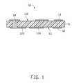
- FIG. 1shows a circuit substrate according to an exemplary embodiment.
- FIG. 2shows an opening defined in the circuit substrate of FIG. 1 .
- FIG. 3shows an anisotropic conductive film formed on the portion of the first wiring layer exposed from the opening of FIG. 2 .
- FIG. 4shows a multilayer substrate with an electrical element and the anisotropic conductive film of FIG. 3 .
- FIG. 5shows a first adhesive sheet, a second adhesive sheet, a first copper layer, and a second copper layer.
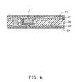
- FIG. 6shows a lamination of the first adhesive sheet, a second adhesive sheet, a first copper layer, a second copper layer of FIG. 5 , and the multilayer substrate of FIG. 4 .
- FIG. 7shows a third wiring layer and a fourth wiring layer converted by the first copper layer and the second copper layer of FIG. 6 .
- FIG. 8shows a first solder mask and a second solder mask formed on the third wiring layer and the fourth wiring layer of FIG. 7 to obtain an embedded printed circuit board.
- a method for manufacturing an embedded printed circuit boardincludes the following steps.
- FIG. 1shows step 1 , in which a circuit substrate 10 is provided.
- the circuit substrate 10includes a base 11 , a first wiring layer 12 , and a second wiring layer 13 .
- the first wiring layer 12 and the second wiring layer 13are respectively arranged at opposite surfaces of the base 11 .
- the base 13is an insulating base, for example rigid resin layer or flexible resin layer.
- the base 13may be a multilayer substrate, and includes a plurality of resin layers and a plurality of wiring layers (not shown). The resin layers and the wiring layers are arranged alternatively.
- the base 11has a first surface 111 and a second surface 112 opposite to the first surface 111 .
- the first wiring layer 12is arranged on the first surface 111 .
- the second wiring layer 13is arranged on the second surface 112 .
- the first wiring layer 12is electrically connected to the second wiring layer 13 via first conductive via 14 in the base 11 .
- the first wiring layer 12 and the second wiring layer 13are formed by an image transfer process and an etching process.
- the first wiring layer 12includes a first electrode connection wire 122 and a second electrode connection wire 124 adjacent to and separated from the first electrode connection wire 122 .
- FIG. 2shows step 2 , in which an opening 15 is defined at a position of the circuit substrate 10 spatially corresponding to the first electrode connection wire 122 and the second electrode connection wire 124 .
- the opening 15only passes through the second wiring layer 13 and the base 11 , and does not pass through the first wiring layer 12 .
- the first electrode connection wire 122 and the second electrode connection wire 124expose outside from the opening 15 .
- the opening 15is configured for receiving an electrical element 17 (see FIG. 4 ).
- the opening 15is formed by laser ablation.
- FIG. 3shows step 3 , in which an anisotropic conductive film 16 is arranged in the opening 15 , and is adhered onto the first electrode connection wire 122 and the second electrode connection wire 124 .
- FIG. 4shows step 4 , in which the electrical element 17 is provided.
- the electrical element 17includes two electrodes 18 and 19 .
- the electrical element 17is adhered to the anisotropic conductive film 16 by a hot pressure method, such that the electrodes 18 and 19 are respectively opposite to the first electrode connection wire 122 and the second electrode connection wire 124 . Accordingly, a multilayer substrate 20 is obtained.
- the electrical element 17is a chip capacitor, and the electrodes 18 and 19 are respectively positive anode and negative anode of the electrical element 17 .
- the anisotropic conductive film 16is conductive along a thickness direction of the anisotropic conductive film 16 , and the surface of the anisotropic conductive film 16 is insulating.
- the thickness direction of the anisotropic conductive film 16is a direction perpendicular to the surfaces of the first electrode connection wire 122 and the second electrode connection wire 124 in the opening 15 , the electrodes 18 and 19 are thus respectively electrically connected to the first electrode connection wire 122 and the second electrode connection wire 124 through the anisotropic conductive film 16 .
- the electrodes of the electrical element 17may be more than two, and the number of the electrode connection wires is same to that of the electrodes of the electrical element 17 . There may be more electrical elements in the circuit substrate 10 , in such case, more openings 15 should be defined in the circuit substrate 10 , and there should be one anisotropic conductive film 16 in each opening 15 .
- FIGS. 5 and 6show step 5 , in which a first adhesive sheet 21 , a second adhesive sheet 22 , a first copper layer 23 , and a second copper layer 24 are provided. Then, the first copper layer 23 , the first adhesive sheet 21 , the multilayer substrate 20 , the second adhesive sheet 22 and the second copper layer 23 are stacked in the described order, and laminated onto each other at the same time.
- materials of the first adhesive sheet 21 and the second adhesive sheet 22are filled into a gap between the electrical element 17 and the circuit substrate 10 , gaps defined in the first wiring layer 12 , and gaps defined in the second wiring layer 13 , such that the first copper layer 23 and the second copper layer 24 are fixed onto the circuit board 10 .
- FIG. 7shows step 6 , in which a second conductive via 211 is formed in the first adhesive sheet 21 , a third conductive via 221 is formed in the second adhesive sheet 22 , and the first copper layer 23 and the second copper layer 24 are respectively converted into a third wiring layer 232 and the fourth wiring layer 242 .
- the second wiring layer 12is electrically connected to the third wiring layer 13 through the second conductive via 211 .
- the first wiring layer 12is electrically connected to the fourth wiring layer 242 through the third conductive via 221 .
- the following stepsmay manufacture the second conductive via 211 : an opening is defined in the first copper layer 23 and the first adhesive sheet 21 by laser ablation; then, the second conductive via 211 is formed by an electroplating process and a via filling process.
- a method of manufacturing the third conductive via 221is same as the method of manufacturing the second conductive via 211 .
- the third wiring layer 232 and the fourth wiring layer 242may be formed by an image transfer process and an etching process.
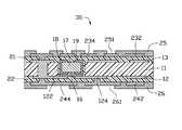
- FIG. 8shows step 7 , in which a first solder mask 25 is formed on the third wiring layer 232 and in gaps defined in the third wiring layer 232 , and a plurality of openings 251 are defined in the first solder mask 25 , thereby enabling portions of the third wiring layer 232 exposed from the openings 251 to serve as contact pads 234 ; a second solder mask 26 is formed on the fourth wiring layer 242 and in gaps defined in the fourth wiring layer 242 , and a plurality of openings 261 are defined in the second solder mask 26 , thereby enabling portions of the fourth wiring layer 242 exposed from the openings 261 to serve as solder pads 244 .
- An embedded printed circuit board 30is thus obtained.
- the contact pads 234are configured for electrically connecting other electrical elements to the third wiring layer 232 .
- the solder pads 244are configured for electrically connecting the fourth wiring layer 242 to other circuit board. In order to prevent the contact pads 234 and the solder pads 244 oxidizing, the surfaces of the contact pads 234 and the solder pads 244 may be covered with golden layers.
- the circuit substrate 10usually includes a plurality of circuit substrate units connecting to each other.
- step 7after a plurality of embedded printed circuit boards 30 are connected to each other are manufactured, there is a cutting step to obtain a plurality of separated embedded printed circuit boards 30 .
- the present embodimentin order to describe easily, only one circuit board 10 and only one embedded printed circuit board 30 are drawn.
- FIG. 8shows that the embedded printed circuit board 30 includes the base 11 , the first wiring layer 12 , the second wiring layer 13 , the first adhesive sheet 21 , the second adhesive 22 , the third wiring layer 232 , the fourth wiring layer 242 , the first solder mask 25 , a second solder mask 26 , the anisotropic conductive film 16 , and the electrical element 17 .
- the first wiring layer 12 and the second wiring layer 13are respectively formed on the first surface 111 and the second surface 112 , and the first wiring layer 12 is electrically connected to the second wiring layer 13 through the first conductive via 14 .
- the first wiring layer 12includes the first electrode connection wire 122 and the second electrode connection wire 124 adjacent to and separated from the first electrode connection wire 122 .
- the opening 15is defined at the position of the base 11 spatially corresponding to the first electrode connection wire 122 and the second electrode connection wire 124 .
- the electrical element 17is received in the opening 15 , and is adhered to the first electrode connection wire 122 and the second electrode connection wire 124 through the anisotropic conductive film 16 .
- the electrodes 18 and 19 of the electrical element 17are respectively adjacent to the first electrode connection wire 122 and the second electrode connection wire 124 , and electrically connected to the first electrode connection wire 122 and the second electrode connection wire 124 through the anisotropic conductive film 16 .
- the first adhesive sheet 21is formed on the second wiring layer 13 .
- the second adhesive sheet 22is formed on the first wiring layer 12 .
- the third wiring layer 132is formed on a side of the first adhesive sheet 21 further away from the second wiring layer 13 .
- the fourth wiring layer 242is formed on a side of the second adhesive sheet 22 further away from the first wiring layer 12 .
- the third wiring layer 232is electrically connected to the second wiring layer 13 through the second conductive via 211 .
- the fourth conductive layer 242is electrically connected to the first conductive layer 12 through the third conductive via 221 .
- the first solder mask 25partially covers the third wiring layer 232 , and exposes the portions of the third wring layer 232 to define the contact pads 2354 .
- the second solder mask 26partially covers the fourth wiring layer 242 , and exposes the portions of the fourth wiring layer 242 to define the solder pads 244 .
- the electrical element 17is electrically connected to the first electrode connection wire 122 and the second electrode connection wire 124 by the anisotropic conductive film 16 .
- a conductive viadoes not need to be formed to electrically connect the electrical element 17 to the first electrode connection wire 122 and the second electrode connection wire 124 .
- no laser ablationis added thereto. The electrical element 17 is thus protected, and production efficiency is thus improved.
Landscapes
- Engineering & Computer Science (AREA)
- Microelectronics & Electronic Packaging (AREA)
- Manufacturing & Machinery (AREA)
- Production Of Multi-Layered Print Wiring Board (AREA)
- Manufacturing Of Printed Wiring (AREA)
Abstract
Description
Claims (10)
Applications Claiming Priority (2)
| Application Number | Priority Date | Filing Date | Title |
|---|---|---|---|
| CN201210432299.9ACN103796445A (en) | 2012-11-02 | 2012-11-02 | Circuit board with buried element, and manufacturing method thereof |
| CN2012104322999 | 2012-11-02 |
Publications (2)
| Publication Number | Publication Date |
|---|---|
| US20140124245A1 US20140124245A1 (en) | 2014-05-08 |
| US9024203B2true US9024203B2 (en) | 2015-05-05 |
Family
ID=50621312
Family Applications (1)
| Application Number | Title | Priority Date | Filing Date |
|---|---|---|---|
| US13/928,701Active2033-11-07US9024203B2 (en) | 2012-11-02 | 2013-06-27 | Embedded printed circuit board and method for manufacturing same |
Country Status (3)
| Country | Link |
|---|---|
| US (1) | US9024203B2 (en) |
| CN (1) | CN103796445A (en) |
| TW (1) | TWI469700B (en) |
Cited By (3)
| Publication number | Priority date | Publication date | Assignee | Title |
|---|---|---|---|---|
| US20140321084A1 (en)* | 2013-04-26 | 2014-10-30 | Samsung Electro-Mechanics Co., Ltd. | Printed circuit board including electronic component embedded therein and method for manufacturing the same |
| US20220240385A1 (en)* | 2021-01-25 | 2022-07-28 | Qi Ding Technology Qinhuangdao Co., Ltd. | Packaged circuit structure and method for manufacturing the same |
| US20230292446A1 (en)* | 2021-10-20 | 2023-09-14 | Qing Ding Precision Electronics (Huaian) Co.,Ltd | Multilayer circuit board with embedded module and method for manufacturing same |
Families Citing this family (11)
| Publication number | Priority date | Publication date | Assignee | Title |
|---|---|---|---|---|
| US10231333B1 (en) | 2013-08-27 | 2019-03-12 | Flextronics Ap, Llc. | Copper interconnect for PTH components assembly |
| US10154583B1 (en) | 2015-03-27 | 2018-12-11 | Flex Ltd | Mechanical strain reduction on flexible and rigid-flexible circuits |
| US10466118B1 (en) | 2015-08-28 | 2019-11-05 | Multek Technologies, Ltd. | Stretchable flexible durable pressure sensor |
| CN108617089B (en)* | 2016-12-10 | 2020-12-22 | 宏启胜精密电子(秦皇岛)有限公司 | Flexible circuit board with embedded element and manufacturing method thereof |
| CN108538799B (en) | 2017-03-02 | 2024-02-27 | 弗莱克斯有限公司 | Interconnect component and interconnect assembly |
| US10535845B1 (en) | 2017-07-14 | 2020-01-14 | Flex Ltd. | Flexible and stretchable chain battery |
| US10426029B1 (en)* | 2018-01-18 | 2019-09-24 | Flex Ltd. | Micro-pad array to thread flexible attachment |
| US10687421B1 (en) | 2018-04-04 | 2020-06-16 | Flex Ltd. | Fabric with woven wire braid |
| US10575381B1 (en) | 2018-06-01 | 2020-02-25 | Flex Ltd. | Electroluminescent display on smart textile and interconnect methods |
| CN113133191B (en)* | 2020-01-15 | 2022-06-24 | 鹏鼎控股(深圳)股份有限公司 | Embedded transparent circuit board and manufacturing method thereof |
| CN113692143B (en)* | 2020-05-19 | 2023-01-17 | 鹏鼎控股(深圳)股份有限公司 | Method for manufacturing circuit board with embedded element |
Citations (2)
| Publication number | Priority date | Publication date | Assignee | Title |
|---|---|---|---|---|
| TW200731889A (en) | 2006-02-13 | 2007-08-16 | Advanced Semiconductor Eng | Method of fabricating substrate with embedded component therein |
| TW200742519A (en) | 2005-10-17 | 2007-11-01 | Samsung Electro Mech | Substrate embedded with passive device |
Family Cites Families (1)
| Publication number | Priority date | Publication date | Assignee | Title |
|---|---|---|---|---|
| CN101594740B (en)* | 2008-05-27 | 2012-06-06 | 华通电脑股份有限公司 | Circuit board with embedded electronic devices and method thereof |
- 2012
- 2012-11-02CNCN201210432299.9Apatent/CN103796445A/enactivePending
- 2012-11-09TWTW101141740Apatent/TWI469700B/enactive
- 2013
- 2013-06-27USUS13/928,701patent/US9024203B2/enactiveActive
Patent Citations (2)
| Publication number | Priority date | Publication date | Assignee | Title |
|---|---|---|---|---|
| TW200742519A (en) | 2005-10-17 | 2007-11-01 | Samsung Electro Mech | Substrate embedded with passive device |
| TW200731889A (en) | 2006-02-13 | 2007-08-16 | Advanced Semiconductor Eng | Method of fabricating substrate with embedded component therein |
Cited By (6)
| Publication number | Priority date | Publication date | Assignee | Title |
|---|---|---|---|---|
| US20140321084A1 (en)* | 2013-04-26 | 2014-10-30 | Samsung Electro-Mechanics Co., Ltd. | Printed circuit board including electronic component embedded therein and method for manufacturing the same |
| US9526177B2 (en)* | 2013-04-26 | 2016-12-20 | Samsung Electro-Mechanics Co., Ltd. | Printed circuit board including electronic component embedded therein and method for manufacturing the same |
| US20220240385A1 (en)* | 2021-01-25 | 2022-07-28 | Qi Ding Technology Qinhuangdao Co., Ltd. | Packaged circuit structure and method for manufacturing the same |
| US11683888B2 (en)* | 2021-01-25 | 2023-06-20 | Leading Interconnect Semiconductor Technology Qinhuangdao Co, Ltd. | Method for manufacturing a packaged circuit structure |
| US12418989B2 (en) | 2021-01-25 | 2025-09-16 | Leading Interconnect Semiconductor Technology Qinhuangdao Co., Ltd. | Packaged circuit structure |
| US20230292446A1 (en)* | 2021-10-20 | 2023-09-14 | Qing Ding Precision Electronics (Huaian) Co.,Ltd | Multilayer circuit board with embedded module and method for manufacturing same |
Also Published As
| Publication number | Publication date |
|---|---|
| CN103796445A (en) | 2014-05-14 |
| TWI469700B (en) | 2015-01-11 |
| TW201419960A (en) | 2014-05-16 |
| US20140124245A1 (en) | 2014-05-08 |
Similar Documents
| Publication | Publication Date | Title |
|---|---|---|
| US9024203B2 (en) | Embedded printed circuit board and method for manufacturing same | |
| US9089082B2 (en) | Printed circuit board with embedded component and method for manufacturing same | |
| US9743533B2 (en) | Method for manufacturing rigid-flexible printed circuit board | |
| US9730328B2 (en) | Printed circuit board with embedded component and method for manufacturing same | |
| EP2705735B1 (en) | Method for manufacturing printed circuit board | |
| US9357647B2 (en) | Packaging substrate, method for manufacturing same, and chip packaging body having same | |
| US20140144675A1 (en) | Multi-layer printed circuit board and method for manufacturing same | |
| US20140036465A1 (en) | Packaging substrate, method for manufacturing same, and chip packaging body having same | |
| US20130341073A1 (en) | Packaging substrate and method for manufacturing same | |
| US20090159559A1 (en) | Method of manufacturing multilayer printed circuit board having buried holes | |
| US20140085833A1 (en) | Chip packaging substrate, method for manufacturing same, and chip packaging structure having same | |
| US20140353006A1 (en) | Multilayer circuit board and method for manufacturing same | |
| KR20150092625A (en) | Embedded printed circuit substrate | |
| EP3291285A1 (en) | Semiconductor package structure with a polymer gel surrounding solders connecting a chip to a substrate and manufacturing method thereof | |
| US9362248B2 (en) | Coreless package structure and method for manufacturing same | |
| TW201228511A (en) | Method for manufacturing multilayer printed circuit board | |
| KR101701380B1 (en) | Device embedded flexible printed circuit board and manufacturing method thereof | |
| US20140182899A1 (en) | Rigid-flexible printed circuit board and method for manufacturing same | |
| KR101905879B1 (en) | The printed circuit board and the method for manufacturing the same | |
| KR101516531B1 (en) | Circuit board, and manufacturing method for circuit board | |
| US20130092420A1 (en) | Embedded multilayer printed circuit board and method | |
| TW201410092A (en) | Rigid-flexible circuit substrate, rigid-flexible circuit board and method for manufacturing same | |
| KR101048515B1 (en) | Electronic printed circuit board and its manufacturing method | |
| JP6863244B2 (en) | Electronic components and manufacturing methods for electronic components | |
| TW201427505A (en) | Printed circuit board having buried component and method for manufacturing same |
Legal Events
| Date | Code | Title | Description |
|---|---|---|---|
| AS | Assignment | Owner name:ZHEN DING TECHNOLOGY CO., LTD., TAIWAN Free format text:ASSIGNMENT OF ASSIGNORS INTEREST;ASSIGNOR:LAI, CHIEN-KUANG;REEL/FRAME:030702/0063 Effective date:20130620 | |
| STCF | Information on status: patent grant | Free format text:PATENTED CASE | |
| AS | Assignment | Owner name:ZHEN DING TECHNOLOGY CO., LTD., TAIWAN Free format text:ASSIGNMENT OF ASSIGNORS INTEREST;ASSIGNOR:ZHEN DING TECHNOLOGY CO., LTD.;REEL/FRAME:039806/0499 Effective date:20160902 Owner name:QI DING TECHNOLOGY QINHUANGDAO CO., LTD., CHINA Free format text:ASSIGNMENT OF ASSIGNORS INTEREST;ASSIGNOR:ZHEN DING TECHNOLOGY CO., LTD.;REEL/FRAME:039806/0499 Effective date:20160902 | |
| MAFP | Maintenance fee payment | Free format text:PAYMENT OF MAINTENANCE FEE, 4TH YEAR, LARGE ENTITY (ORIGINAL EVENT CODE: M1551); ENTITY STATUS OF PATENT OWNER: LARGE ENTITY Year of fee payment:4 | |
| MAFP | Maintenance fee payment | Free format text:PAYMENT OF MAINTENANCE FEE, 8TH YEAR, LARGE ENTITY (ORIGINAL EVENT CODE: M1552); ENTITY STATUS OF PATENT OWNER: LARGE ENTITY Year of fee payment:8 | |
| AS | Assignment | Owner name:ZHEN DING TECHNOLOGY CO., LTD., TAIWAN Free format text:ASSIGNMENT OF ASSIGNORS INTEREST;ASSIGNORS:QI DING TECHNOLOGY QINHUANGDAO CO., LTD.;ZHEN DING TECHNOLOGY CO., LTD.;REEL/FRAME:064899/0050 Effective date:20230801 Owner name:LEADING INTERCONNECT SEMICONDUCTOR TECHNOLOGY QINHUANGDAO CO., LTD., CHINA Free format text:ASSIGNMENT OF ASSIGNORS INTEREST;ASSIGNORS:QI DING TECHNOLOGY QINHUANGDAO CO., LTD.;ZHEN DING TECHNOLOGY CO., LTD.;REEL/FRAME:064899/0050 Effective date:20230801 |