US9023691B2 - Microelectronic assemblies with stack terminals coupled by connectors extending through encapsulation - Google Patents
Microelectronic assemblies with stack terminals coupled by connectors extending through encapsulationDownload PDFInfo
- Publication number
- US9023691B2 US9023691B2US13/942,568US201313942568AUS9023691B2US 9023691 B2US9023691 B2US 9023691B2US 201313942568 AUS201313942568 AUS 201313942568AUS 9023691 B2US9023691 B2US 9023691B2
- Authority
- US
- United States
- Prior art keywords
- connectors
- microelectronic
- encapsulation
- support element
- assembly
- Prior art date
- Legal status (The legal status is an assumption and is not a legal conclusion. Google has not performed a legal analysis and makes no representation as to the accuracy of the status listed.)
- Active
Links
Images


Classifications
- H—ELECTRICITY
- H01—ELECTRIC ELEMENTS
- H01L—SEMICONDUCTOR DEVICES NOT COVERED BY CLASS H10
- H01L23/00—Details of semiconductor or other solid state devices
- H01L23/28—Encapsulations, e.g. encapsulating layers, coatings, e.g. for protection
- H—ELECTRICITY
- H01—ELECTRIC ELEMENTS
- H01L—SEMICONDUCTOR DEVICES NOT COVERED BY CLASS H10
- H01L23/00—Details of semiconductor or other solid state devices
- H01L23/48—Arrangements for conducting electric current to or from the solid state body in operation, e.g. leads, terminal arrangements ; Selection of materials therefor
- H01L23/488—Arrangements for conducting electric current to or from the solid state body in operation, e.g. leads, terminal arrangements ; Selection of materials therefor consisting of soldered or bonded constructions
- H01L23/498—Leads, i.e. metallisations or lead-frames on insulating substrates, e.g. chip carriers
- H01L23/49811—Additional leads joined to the metallisation on the insulating substrate, e.g. pins, bumps, wires, flat leads
- H—ELECTRICITY
- H01—ELECTRIC ELEMENTS
- H01L—SEMICONDUCTOR DEVICES NOT COVERED BY CLASS H10
- H01L21/00—Processes or apparatus adapted for the manufacture or treatment of semiconductor or solid state devices or of parts thereof
- H01L21/02—Manufacture or treatment of semiconductor devices or of parts thereof
- H01L21/04—Manufacture or treatment of semiconductor devices or of parts thereof the devices having potential barriers, e.g. a PN junction, depletion layer or carrier concentration layer
- H01L21/50—Assembly of semiconductor devices using processes or apparatus not provided for in a single one of the groups H01L21/18 - H01L21/326 or H10D48/04 - H10D48/07 e.g. sealing of a cap to a base of a container
- H01L21/56—Encapsulations, e.g. encapsulation layers, coatings
- H—ELECTRICITY
- H01—ELECTRIC ELEMENTS
- H01L—SEMICONDUCTOR DEVICES NOT COVERED BY CLASS H10
- H01L25/00—Assemblies consisting of a plurality of semiconductor or other solid state devices
- H01L25/03—Assemblies consisting of a plurality of semiconductor or other solid state devices all the devices being of a type provided for in a single subclass of subclasses H10B, H10D, H10F, H10H, H10K or H10N, e.g. assemblies of rectifier diodes
- H01L25/10—Assemblies consisting of a plurality of semiconductor or other solid state devices all the devices being of a type provided for in a single subclass of subclasses H10B, H10D, H10F, H10H, H10K or H10N, e.g. assemblies of rectifier diodes the devices having separate containers
- H01L25/105—Assemblies consisting of a plurality of semiconductor or other solid state devices all the devices being of a type provided for in a single subclass of subclasses H10B, H10D, H10F, H10H, H10K or H10N, e.g. assemblies of rectifier diodes the devices having separate containers the devices being integrated devices of class H10
- H—ELECTRICITY
- H01—ELECTRIC ELEMENTS
- H01L—SEMICONDUCTOR DEVICES NOT COVERED BY CLASS H10
- H01L2224/00—Indexing scheme for arrangements for connecting or disconnecting semiconductor or solid-state bodies and methods related thereto as covered by H01L24/00
- H01L2224/01—Means for bonding being attached to, or being formed on, the surface to be connected, e.g. chip-to-package, die-attach, "first-level" interconnects; Manufacturing methods related thereto
- H01L2224/10—Bump connectors; Manufacturing methods related thereto
- H01L2224/15—Structure, shape, material or disposition of the bump connectors after the connecting process
- H01L2224/16—Structure, shape, material or disposition of the bump connectors after the connecting process of an individual bump connector
- H01L2224/161—Disposition
- H01L2224/16151—Disposition the bump connector connecting between a semiconductor or solid-state body and an item not being a semiconductor or solid-state body, e.g. chip-to-substrate, chip-to-passive
- H01L2224/16221—Disposition the bump connector connecting between a semiconductor or solid-state body and an item not being a semiconductor or solid-state body, e.g. chip-to-substrate, chip-to-passive the body and the item being stacked
- H01L2224/16225—Disposition the bump connector connecting between a semiconductor or solid-state body and an item not being a semiconductor or solid-state body, e.g. chip-to-substrate, chip-to-passive the body and the item being stacked the item being non-metallic, e.g. insulating substrate with or without metallisation
- H—ELECTRICITY
- H01—ELECTRIC ELEMENTS
- H01L—SEMICONDUCTOR DEVICES NOT COVERED BY CLASS H10
- H01L2224/00—Indexing scheme for arrangements for connecting or disconnecting semiconductor or solid-state bodies and methods related thereto as covered by H01L24/00
- H01L2224/01—Means for bonding being attached to, or being formed on, the surface to be connected, e.g. chip-to-package, die-attach, "first-level" interconnects; Manufacturing methods related thereto
- H01L2224/26—Layer connectors, e.g. plate connectors, solder or adhesive layers; Manufacturing methods related thereto
- H01L2224/31—Structure, shape, material or disposition of the layer connectors after the connecting process
- H01L2224/32—Structure, shape, material or disposition of the layer connectors after the connecting process of an individual layer connector
- H01L2224/321—Disposition
- H01L2224/32151—Disposition the layer connector connecting between a semiconductor or solid-state body and an item not being a semiconductor or solid-state body, e.g. chip-to-substrate, chip-to-passive
- H01L2224/32221—Disposition the layer connector connecting between a semiconductor or solid-state body and an item not being a semiconductor or solid-state body, e.g. chip-to-substrate, chip-to-passive the body and the item being stacked
- H01L2224/32225—Disposition the layer connector connecting between a semiconductor or solid-state body and an item not being a semiconductor or solid-state body, e.g. chip-to-substrate, chip-to-passive the body and the item being stacked the item being non-metallic, e.g. insulating substrate with or without metallisation
- H—ELECTRICITY
- H01—ELECTRIC ELEMENTS
- H01L—SEMICONDUCTOR DEVICES NOT COVERED BY CLASS H10
- H01L2224/00—Indexing scheme for arrangements for connecting or disconnecting semiconductor or solid-state bodies and methods related thereto as covered by H01L24/00
- H01L2224/73—Means for bonding being of different types provided for in two or more of groups H01L2224/10, H01L2224/18, H01L2224/26, H01L2224/34, H01L2224/42, H01L2224/50, H01L2224/63, H01L2224/71
- H01L2224/732—Location after the connecting process
- H01L2224/73201—Location after the connecting process on the same surface
- H01L2224/73203—Bump and layer connectors
- H01L2224/73204—Bump and layer connectors the bump connector being embedded into the layer connector
- H—ELECTRICITY
- H01—ELECTRIC ELEMENTS
- H01L—SEMICONDUCTOR DEVICES NOT COVERED BY CLASS H10
- H01L2225/00—Details relating to assemblies covered by the group H01L25/00 but not provided for in its subgroups
- H01L2225/03—All the devices being of a type provided for in the same main group of the same subclass of class H10, e.g. assemblies of rectifier diodes
- H01L2225/10—All the devices being of a type provided for in the same main group of the same subclass of class H10, e.g. assemblies of rectifier diodes the devices having separate containers
- H01L2225/1005—All the devices being of a type provided for in the same main group of the same subclass of class H10, e.g. assemblies of rectifier diodes the devices having separate containers the devices being integrated devices of class H10
- H01L2225/1011—All the devices being of a type provided for in the same main group of the same subclass of class H10, e.g. assemblies of rectifier diodes the devices having separate containers the devices being integrated devices of class H10 the containers being in a stacked arrangement
- H01L2225/1017—All the devices being of a type provided for in the same main group of the same subclass of class H10, e.g. assemblies of rectifier diodes the devices having separate containers the devices being integrated devices of class H10 the containers being in a stacked arrangement the lowermost container comprising a device support
- H01L2225/1023—All the devices being of a type provided for in the same main group of the same subclass of class H10, e.g. assemblies of rectifier diodes the devices having separate containers the devices being integrated devices of class H10 the containers being in a stacked arrangement the lowermost container comprising a device support the support being an insulating substrate
- H—ELECTRICITY
- H01—ELECTRIC ELEMENTS
- H01L—SEMICONDUCTOR DEVICES NOT COVERED BY CLASS H10
- H01L2225/00—Details relating to assemblies covered by the group H01L25/00 but not provided for in its subgroups
- H01L2225/03—All the devices being of a type provided for in the same main group of the same subclass of class H10, e.g. assemblies of rectifier diodes
- H01L2225/10—All the devices being of a type provided for in the same main group of the same subclass of class H10, e.g. assemblies of rectifier diodes the devices having separate containers
- H01L2225/1005—All the devices being of a type provided for in the same main group of the same subclass of class H10, e.g. assemblies of rectifier diodes the devices having separate containers the devices being integrated devices of class H10
- H01L2225/1011—All the devices being of a type provided for in the same main group of the same subclass of class H10, e.g. assemblies of rectifier diodes the devices having separate containers the devices being integrated devices of class H10 the containers being in a stacked arrangement
- H01L2225/1041—Special adaptations for top connections of the lowermost container, e.g. redistribution layer, integral interposer
- H—ELECTRICITY
- H01—ELECTRIC ELEMENTS
- H01L—SEMICONDUCTOR DEVICES NOT COVERED BY CLASS H10
- H01L2225/00—Details relating to assemblies covered by the group H01L25/00 but not provided for in its subgroups
- H01L2225/03—All the devices being of a type provided for in the same main group of the same subclass of class H10, e.g. assemblies of rectifier diodes
- H01L2225/10—All the devices being of a type provided for in the same main group of the same subclass of class H10, e.g. assemblies of rectifier diodes the devices having separate containers
- H01L2225/1005—All the devices being of a type provided for in the same main group of the same subclass of class H10, e.g. assemblies of rectifier diodes the devices having separate containers the devices being integrated devices of class H10
- H01L2225/1011—All the devices being of a type provided for in the same main group of the same subclass of class H10, e.g. assemblies of rectifier diodes the devices having separate containers the devices being integrated devices of class H10 the containers being in a stacked arrangement
- H01L2225/1047—Details of electrical connections between containers
- H01L2225/1058—Bump or bump-like electrical connections, e.g. balls, pillars, posts
- H—ELECTRICITY
- H01—ELECTRIC ELEMENTS
- H01L—SEMICONDUCTOR DEVICES NOT COVERED BY CLASS H10
- H01L23/00—Details of semiconductor or other solid state devices
- H01L23/28—Encapsulations, e.g. encapsulating layers, coatings, e.g. for protection
- H01L23/31—Encapsulations, e.g. encapsulating layers, coatings, e.g. for protection characterised by the arrangement or shape
- H01L23/3107—Encapsulations, e.g. encapsulating layers, coatings, e.g. for protection characterised by the arrangement or shape the device being completely enclosed
- H01L23/3121—Encapsulations, e.g. encapsulating layers, coatings, e.g. for protection characterised by the arrangement or shape the device being completely enclosed a substrate forming part of the encapsulation
- H01L23/3128—Encapsulations, e.g. encapsulating layers, coatings, e.g. for protection characterised by the arrangement or shape the device being completely enclosed a substrate forming part of the encapsulation the substrate having spherical bumps for external connection
Definitions
- the present inventionrelates to packaging of microelectronic elements, especially the packaging of semiconductor chips.
- Microelectronic elementsgenerally comprise a thin slab of a semiconductor material, such as silicon or gallium arsenide, commonly called a die or a semiconductor chip.
- Semiconductor chipsare commonly provided as individual, prepackaged units. In some unit designs, the semiconductor chip is mounted to a substrate or chip carrier, which is in turn mounted on a circuit panel, such as a printed circuit board.
- the active circuitryis fabricated in a first face of the semiconductor chip (e.g., a front surface).
- the chipis provided with bond pads on the same face.
- the bond padsare typically placed in a regular array either around the edges of the die or, for many memory devices, in the die center.
- the bond padsare generally made of a conductive metal, such as copper, or aluminum, around 0.5 micron ( ⁇ m) thick.
- the bond padscould include a single layer or multiple layers of metal.
- the size of the bond padswill vary with the device type but will typically measure tens to hundreds of microns on a side.
- Microelectronic elementssuch as semiconductor chips typically require many input and output connections to other electronic components.
- the input and output contacts of a semiconductor chip or other comparable deviceare generally disposed in grid-like patterns that substantially cover a surface of the chip (commonly referred to as an “area array”) or in elongated rows which may extend parallel to and adjacent each edge of the chip's front surface, or in the center of the front surface.
- Semiconductor chipsare commonly provided in packages that facilitate handling of the chip during manufacture and during mounting of the chip on an external substrate such as a circuit board or other circuit panel. For example, many semiconductor chips are provided in packages suitable for surface mounting. Numerous packages of this general type have been proposed for various applications.
- such packagesinclude a dielectric element, commonly referred to as a “chip carrier” with terminals formed as plated or etched metallic structures on the dielectric. These terminals typically are connected to the contacts of the chip itself by features such as thin traces extending along the chip carrier itself and by fine leads or wires extending between the contacts of the chip and the terminals or traces.
- the packageis placed onto a circuit board so that each terminal on the package is aligned with a corresponding contact pad on the circuit board. Solder or other bonding material is provided between the terminals and the contact pads.
- the packagecan be permanently bonded in place by heating the assembly so as to melt or “reflow” the solder or otherwise activate the bonding material.
- solder massesin the form of solder balls, typically about 0.1 mm and about 0.8 mm (5 and 30 mils) in diameter, attached to the terminals of the package.
- a package having an array of solder balls projecting from its bottom surfaceis commonly referred to as a ball grid array or “BGA” package.
- Other packages, referred to as land grid array or “LGA” packagesare secured to the substrate by thin layers or lands formed from solder.
- Packages of this typecan be quite compact.
- Certain packages, commonly referred to as “chip scale packages,”occupy an area of the circuit board equal to, or only slightly larger than, the area of the device incorporated in the package. This is advantageous in that it reduces the overall size of the assembly and permits the use of short interconnections between various devices on the substrate, which in turn limits signal propagation time between devices and thus facilitates operation of the assembly at high speeds.
- Packaged semiconductor chipsare often provided in “stacked” arrangements, wherein one package is provided, for example, on a circuit board, and another package is mounted on top of the first package. These arrangements can allow a number of different chips to be mounted within a single footprint on a circuit board and can further facilitate high-speed operation by providing a short interconnection between packages. Often, this interconnect distance is only slightly larger than the thickness of the chip itself.
- For interconnection to be achieved within a stack of chip packagesit is necessary to provide structures for mechanical and electrical connection on both sides of each package (except for the topmost package). This has been done, for example, by providing contact pads or lands on both sides of the substrate to which the chip is mounted, the pads being connected through the substrate by conductive vias or the like. Examples of stacked chip arrangements and interconnect structures are provided in U.S. Patent App. Pub. No. 2010/0232129, the disclosure of which is incorporated by reference herein.
- Sizeis a significant consideration in any physical arrangement of chips.
- devices commonly referred to as “smart phones”integrate the functions of a cellular telephone with powerful data processors, memory and ancillary devices such as global positioning system receivers, electronic cameras, and local area network connections along with high-resolution displays and associated image processing chips.
- Such devicescan provide capabilities such as full internet connectivity, entertainment including full-resolution video, navigation, electronic banking and more, all in a pocket-size device.
- Complex portable devicesrequire packing numerous chips into a small space.
- I/O'sinput and output connections
- the interconnectionsshould be short and should have low impedance to minimize signal propagation delays.
- the components which form the interconnectionsshould not greatly increase the size of the assembly. Similar needs arise in other applications as, for example, in data servers such as those used in internet search engines. For example, structures which provide numerous short, low-impedance interconnects between complex chips can increase the bandwidth of the search engine and reduce its power consumption.
- a microelectronic assemblywhich includes first and second support elements, each of which has first and second oppositely facing surfaces.
- a microelectronic elementcan be mounted to the second surface of a support element of the first and second support elements.
- Electrically conductive first connectorsmay project above the second surface of the first support element, and electrically conductive second connectors may project above the second surface of the second support element, such second connectors which can be coupled to ends of the first connectors.
- the assemblycan further include an encapsulation formed in contact with the second surface of a support element of the first and second support elements, and which can be formed in contact with at least one of: the second surface of another support element of the first and second support elements; or a second encapsulation formed in contact with the second surface of the another support element.
- Respective pairs of coupled first and second connectorscan be separated from one another and from the microelectronic element by material of the encapsulation.
- First package terminals at the first surface of the first support elementcan be electrically coupled with corresponding second package terminals at the first surface of the second support element through pairs of said first connectors aligned with and joined with said second connectors.
- at least one of: the first connectors, and the second connectorscan include electrically conductive masses.
- a standoff height between the second surfaces of the support elementsis greater than a pitch of the first connectors in at least one direction parallel to the second surface of the first support element.
- the standoff heightcan be equal to or greater than 1.5 times the pitch.
- the microelectronic elementcan have a face facing away from the support element to which it is mounted, and the encapsulation can be formed in contact with at least one of: the face of the microelectronic element or a third encapsulation formed on the face of the microelectronic element.
- the microelectronic assemblycan include the second encapsulation and the encapsulation can be formed in contact with the second encapsulation.
- the microelectronic assemblycan include the second encapsulation, the second encapsulation can be formed in contact with the face of the microelectronic element and the second and third encapsulations can be the same encapsulation.
- the first connectors and the second connectorscan have ends at maximum heights above the second surface of the first and second support elements, respectively, and the ends of the first connectors can be aligned with and joined to ends of the second connectors.
- the first and second connectorscan consist essentially of solder.
- At least one of the first connectors or the second connectorscan include solid wettable non-solder cores and solder coatings at least substantially covering the cores.
- At least one of the first connectors or the second connectorscan include at least one of: stud bumps or solid substantially rigid metal posts.
- the first connectorscan include stud bumps and the second connectors can include stud bumps.
- the first connectorscan include solid substantially rigid metal posts and the second connectors can include solid substantially rigid metal posts.
- the first connectorscan include solid substantially rigid metal posts and the second connectors can include solid substantially rigid metal posts.
- a stacked multi-chip microelectronic assemblycan include a microelectronic package overlying the first support element of the microelectronic assembly, the microelectronic package having terminals connected with the first package terminals of the microelectronic assembly.
- the first connectorscan be conductive metal masses and the second connectors can include solid substantially rigid metal posts.
- each of the conductive metal massescan be surrounded by the encapsulation.
- each of the metal postscan be surrounded by the third encapsulation.
- the second connectorscan be conductive metal masses, each of the conductive metal masses can be surrounded by the encapsulation, and the first connectors can include solid substantially rigid metal posts.
- the microelectronic assemblymay include third connectors each aligned with an end of one of the first connectors and with an end of one of the second connectors and being joined with at least one of the aligned first and second connectors, wherein coupled first, second and third connectors can be aligned in respective columns and the columns can be separated from one another and from the microelectronic element by the material of the encapsulation, and the first package terminals can be electrically coupled with the corresponding second package terminals through the third connectors.
- the encapsulationmay separate and insulate individual third connectors from one another.
- the microelectronic assemblymay include dielectric reinforcing collars overlying surfaces of some of at least one of: the first connectors, or the second connectors, wherein the encapsulation overlies the reinforcing collars.
- the dielectric reinforcing collarstypically rise along surfaces of respective individual connectors and may form troughs between adjacent collars.
- the reinforcing collarscan be made of an underfill material.
- a microelectronic assemblywhich can include first and second support elements each having first and second oppositely facing surfaces, and a microelectronic element mounted to the second surface of a support element of the first and second support elements.
- Electrically conductive first connectorsmay project above the second surface of the first support element
- electrically conductive second connectorsmay project above the second surface of the second support element and may be coupled to ends of the first connectors.
- An encapsulationcan be formed in contact with the second surfaces of the first and second support elements and can encapsulate the microelectronic element and respective pairs of coupled first and second connectors.
- First package terminals at the first surface of the first support elementcan be electrically coupled with corresponding second package terminals at the first surface of the second support element through pairs of said first connectors aligned with and joined with the second connectors.
- the pairs of coupled first and second connectorscan include substantially rigid solid metal posts and metal interconnects plated onto and projecting upwardly above end surface of the metal posts.
- a method of fabricating a microelectronic assembly according to another aspect of the inventioncan include joining first and second subassemblies to form an assembly having first terminals at a first outwardly facing surface of the assembly and second terminals at a second outwardly facing surface of the assembly opposite from the first surface. At least one of the subassemblies can have at least one microelectronic element mounted to an inwardly facing second surface thereof. The microelectronic element can be electrically coupled to the at least one subassembly.
- the first subassemblycan include a first support element
- the second subassemblycan include a second support element
- at least one of the first or second subassembliescan include connectors projecting above the inwardly facing second surface of such support element towards the inwardly facing second surface of the other support element.
- Each of a plurality of the first terminalscan be electrically coupled with respective second terminals through a respective pair of a first connector having an end coupled with an end of a corresponding second connector, the first connector extending above the second connector.
- An encapsulantcan be flowed into a space between the first and second support elements so as to form an encapsulation separating at least portions of individual pairs of joined first and second connectors from one another.
- At least one of: the first connectors or the second connectorsare constrained during the joining process to maintain a height of such connectors during the joining process.
- solder connectorstend to collapse during joining.
- An encapsulation or reinforcing collars surrounding individual connectorscan help maintain their heights during a joining process.
- the samecan help avoid the widths of individual connectors, e.g., conductive masses such as solder from expanding during joining.
- the microelectronic elementhas a face facing away from the support element to which the microelectronic element can be mounted, and the encapsulation can be formed in contact with at least one of: the face of the microelectronic element or a third encapsulation which adheres to the face of the microelectronic element.
- one of the first or second subassembliescan include a second encapsulation separating the connectors thereof from one another and the encapsulation can be formed in contact with the second encapsulation.
- the microelectronic assemblycan include the second encapsulation, the second encapsulation can be formed in contact with the face of the microelectronic element and the second and third encapsulations can be the same encapsulation.
- the first connectors and the second connectorscan have ends at maximum heights above the second surface of the first and second support elements, respectively, and the ends of the first connectors can be aligned with and joined directly with ends of the second connectors.
- the first and second connectorscan consist essentially of solder.
- the first connectorscan be conductive metal masses and the second connectors can include solid substantially rigid metal posts.
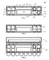
- FIG. 1Ais a sectional view illustrating a microelectronic package according to an embodiment of the invention.
- FIG. 1Bis a top-down plan view illustrating an example of the microelectronic package of FIG. 1A looking towards a plurality of terminals at a surface of a support element thereof.
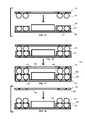
- FIG. 2is a sectional view illustrating a microelectronic package according to an embodiment of the invention.
- FIG. 3is a sectional view illustrating a microelectronic assembly according to an embodiment of the invention.
- FIG. 4Ais a sectional view illustrating a microelectronic package according to a variation of the embodiment of the invention seen in FIGS. 1A-B .
- FIG. 4Bis a top-down plan view illustrating an example of the microelectronic package of FIG. 4A looking towards stack terminals at a surface of a support element thereof.
- FIG. 5is a sectional view illustrating a microelectronic package according to an embodiment of the invention.
- FIG. 6is a sectional view illustrating a microelectronic package according to an embodiment of the invention.
- FIG. 7is a sectional view illustrating a microelectronic package according to an embodiment of the invention.
- FIG. 8is a sectional view illustrating a microelectronic assembly according to an embodiment of the invention.
- FIG. 9is a sectional view illustrating a microelectronic package according to an embodiment of the invention.
- FIG. 10is a sectional view illustrating a microelectronic package according to an embodiment of the invention.
- FIG. 11is a sectional view illustrating a stage in a method of making a microelectronic package according to an embodiment of the invention.
- FIG. 12is a sectional view illustrating a stage in a method of making a microelectronic package according to an embodiment of the invention subsequent to the stage of FIG. 11 .
- FIG. 13is a sectional view illustrating a stage in a method of making a microelectronic package according to an embodiment of the invention subsequent to the stage of FIG. 12 .
- FIG. 14is a sectional view illustrating a stage in a method of making a microelectronic package according to a variation of the embodiment shown in FIG. 11 .
- FIG. 15is a sectional view illustrating a stage in a method of making a microelectronic package according to an embodiment of the invention.
- FIG. 16is a sectional view illustrating a stage in a method of making a microelectronic package according to an embodiment of the invention subsequent to the stage of FIG. 15 .
- FIG. 17is a sectional view illustrating a stage in a method of making a microelectronic package according to an embodiment of the invention subsequent to the stage of FIG. 16 .
- FIG. 18is a sectional view illustrating a stage in a method of making a microelectronic package according to a variation of the embodiment shown in FIG. 15 .
- FIG. 19is a sectional view illustrating a microelectronic package according to an embodiment of the invention.
- FIG. 20is a sectional view illustrating a microelectronic package according to an embodiment of the invention.
- FIG. 21illustrates a stage in a method of fabricating a microelectronic assembly according to an embodiment of the invention.
- FIG. 22illustrates a microelectronic assembly formed according to the method depicted in FIG. 21 .
- FIG. 23illustrates a variation of the method of fabrication depicted in FIG. 21 .
- FIG. 24illustrates a variation of the method of fabricating a microelectronic assembly seen in FIG. 21 .
- FIG. 25illustrates a microelectronic assembly formed according to the method depicted in FIG. 24 .
- FIG. 26illustrates a stage in a method of fabricating a microelectronic assembly according to a variation of the embodiment seen in FIGS. 11-14 .
- FIG. 27illustrates a microelectronic assembly formed from the method depicted in FIG. 26 .
- FIGS. 28-29illustrate stages in a method of fabricating a microelectronic assembly according to a variation of the embodiment seen in FIGS. 11-14 .
- FIG. 30illustrates a microelectronic assembly formed according to the method depicted in FIGS. 28-29 .
- FIG. 31is a sectional view illustrating a microelectronic package or assembly as further utilized in a system in accordance with an embodiment of the invention.
- embodiments of the invention hereincan provide improved assemblies containing microelectronic elements and having first terminals and second terminals, e.g., top terminals and bottom terminals, in which vertical interconnects which electrically couple the top terminals and bottom terminals provides desirable standoff height while also allowing the vertical interconnects to be tightly packed with desirable pitch in horizontal directions parallel to a face of the microelectronic element in the assembly.
- a standoff height H between the second surfaces of the support elementsis greater than a pitch “a” of the first connectors in at least one direction parallel to the second surface of the first support element.
- the standoff heightcan be equal to or greater than 1.5 times the pitch.
- the microelectronic packageincludes a first support element 102 and a second support element 104 .
- Each support elementcan be, e.g., a package substrate such as a chip carrier or dielectric element or structure which combines two or more of dielectric, semiconductor and electrically conductive materials on which electrically conductive structure such as terminals, traces, contacts, and vias can be provided.
- one or both support elementscan be or include a sheet-like or board-like dielectric element which comprises at least one of inorganic or organic dielectric material, and which may include primarily inorganic material, or primarily polymeric material, or which may be a composite structure comprising both inorganic and polymeric materials.
- one or both support elementsmay comprise a dielectric element which includes polymeric material such as polyimide, polyamide, epoxy, thermoplastic material, thermoset materials, among others.
- one or both support elementsmay comprise a dielectric element which includes an inorganic dielectric material such as an oxide of silicon, a nitride of silicon, a carbide of silicon, silicon oxynitride, alumina, and one or both support elements can include a semiconductor material such as silicon, germanium, or carbon, among others, or a combination of one or more such inorganic materials.
- one or both support elementscan comprise a dielectric element which is a combination of one or more polymeric materials and one or more inorganic materials, such as the materials described above.
- one or both support elementscan have a structure of glass-reinforced epoxy such as commonly referred to as “FR-4” or “BT resin” board structures.
- one or both support elementsmay consist essentially of polymeric material such as polyimide, for example.
- One or both support elementsmay include one or more layers of compliant material, which in some cases may be exposed at the first surface, the second surface, or both the first and second surfaces of such support element.
- the compliant materialin some cases can comprise polyimide, polyamide which typically have Young modulus less than 2.0 gigapascals (“GPa”), or in some cases the compliant material may include an elastomer having a Young's modulus which is significantly lower, e.g., well below 1.0 GPa.
- each support elementhas first and second oppositely facing surfaces. As assembled in the package 10 , first surfaces 101 , 105 of the support elements face outwardly away from one another, and the second surfaces 103 , 106 face inwardly towards one another.
- a microelectronic element 120which may be an unpackaged or packaged semiconductor chip is mounted to the second surface of one or both of the support elements 102 , 104 .
- the microelectronic elementcan be a semiconductor chip having additional electrically conductive structure at a face thereof coupled to pads of the chip.
- a second microelectronic elementcan be mounted in a space above a surface 129 of the microelectronic element 120 which faces away from support element 104 .
- the second microelectronic elementcan be positioned between surface 129 and the surface 103 of the first support element 102 .
- the microelectronic elementcan be electrically coupled with conductive elements at a surface 106 of the second support element 104 .
- a statement that an electrically conductive element is “at” a surface of a componentindicates that, when the component is not assembled with any other element, the electrically conductive element is available for contact with a theoretical point moving in a direction perpendicular to the surface of the component toward the surface of the component from outside the component.
- a terminal or other conductive element which is at a surface of a substratemay project from such surface; may be flush with such surface; or may be recessed relative to such surface in a hole or depression in the substrate.
- the “surface” of the componentmay be a surface of dielectric structure; however, in particular embodiments, the surface may be a surface of other material such as metal or other electrically conductive material or semiconductor material.
- the directions 180 perpendicular to the first surfaceare referred to herein as upward or downward directions and are also referred to herein as the “vertical” directions.
- the directions referred to hereinare in the frame of reference of the structures referred to. Thus, these directions may lie at any orientation to the normal or gravitational frame of reference.
- a statement that one feature is disposed at a greater height “above a surface” than another featuremeans that the one feature is at a greater distance in the same orthogonal direction away from the surface than the other feature.
- a statement that one feature is disposed at a lesser height “above a surface” than another featuremeans that the one feature is at a smaller distance in the same orthogonal direction away from the surface than the other feature.
- the microelectronic element 120may be flip-chip connected to contacts 126 at surface 106 of support element 104 .
- Microelectronic element 120has a plurality of contacts 124 at the front face 122 which face towards the second surface 106 of second support element 104 , the contacts 124 facing and joined with corresponding contacts 126 of the second support element through bumps 121 that can include bond metal, or which can include other types of joining elements such as micropillars, posts, among others.
- the contactscan be arranged at the front face 122 in one or more rows extending in a first direction, one or more columns extending in a second direction transverse to the first direction, or in both one or more rows and one or more columns.
- Such contactscan be disposed at any positions in directions 178 , 179 or may be disposed in one or more rows, one or more columns, or in one or more rows and in one or more columns adjacent to one or more edges 127 of the microelectronic element.
- the contacts 124can be distributed across at least a portion of the front face of the microelectronic element in an area array having two or more rows of contacts and having two or more columns of contacts.
- An underfill 115may be disposed surrounding individual ones of the connections, e.g., bumps 121 , which in some cases may mechanically reinforce the connections.
- the contacts 124can be arranged at positions within one or more rows of contacts and/or one or more columns of contacts which are aligned with an aperture or “bond window” (not shown) that extends between the first and second surfaces 105 , 106 of the support element 104 .
- the contacts 124 of the microelectronic elementcan be coupled with terminals, e.g., terminals 142 , 142 ′ at the first surface 105 of the second support element 104 through leads which are joined to the contacts 124 .
- the leadscan be wire leads (not shown), e.g., wire bonds, which extend through the aperture and are joined to the contacts 124 and to corresponding contacts (not shown) at the first surface 105 .
- the leadscan be leads each of which includes an first portion extending as a trace along the first or second surfaces 105 , 106 and a second portion integral with the first portion which extends from the trace into the area of the aperture and is joined to the contact.
- a rear surface 129 of the microelectronic elementcan be back-bonded to the second surface 106 of the second support element and the front face 122 of the microelectronic can instead face away from the first surface 106 of support element 104 , with the contacts 124 of the microelectronic element facing away from the second surface 106 .
- the contacts 124can be electrically coupled with corresponding contacts at the second surface 106 of the second support element through conductive structure which extends above the front face 122 and which extends beyond edges 127 of the microelectronic element.
- the microelectronic package 10can include a monolithic encapsulation 150 which is formed in contact with the second surface 103 , or 106 of a support element of the first and second support elements, and which is formed in contact with at least one of: the second surface of another support element of the first and second support elements, and a second encapsulation which is formed in contact with the second surface of the another support element.
- the encapsulation 150can be formed in contact with the second surfaces 103 , 106 of each of the first and second support elements 102 , 104 .
- microelectronic package 10includes pairs of electrically conductive first connectors 161 projecting above the second surface 103 of the first support element 102 which are aligned with and which are mechanically and electrically coupled with corresponding electrically conductive second connectors 162 projecting above the second surface 106 of the second support element 104 .
- First package terminals 141 at the first surface 101 of the first support element 102are electrically coupled with corresponding second package terminals 142 at the first surface 105 of the second support element 104 through respective pairs of the first connectors 161 which are aligned with and electronically coupled with, e.g., joined with the second connectors 162 .
- the first connectors and the second connectorsinclude electrically conductive masses, such as masses of a bond metal, e.g., tin, indium, solder or a eutectic material, or a conductive matrix material of metal particles embedded in a polymeric material.
- the first connectors, the second connectors, or bothcan consist essentially of solder.
- the first connectors and the second connectorscan each include a bond metal.
- one or both of the first and second connectorsmay include a solid core, e.g., core 171 or core 172 over which a bond metal can be provided.
- Solid cores 171 , 172can be used to facilitate or maintain a predetermined spacing between the second surfaces 103 , 106 of the first and second support elements 102 , 104 .
- Solid corescan be of electrically conductive, semiconducting or dielectric material or a combination of one or more such materials.
- the solid corescan be made of non-solder material that is wettable by solder and can be coated with solder.
- a solid coremay consist essentially of copper or other electrically conductive material having a melting point higher than a joining temperature at which the first and second connectors are joined to one another, as will be described below.
- the solid corescan comprise or consist essentially of a solder which has a melting point higher than the joining temperature, and thus may have a higher melting point than the melting point of a solder that coats the solid cores.
- a solid coremay consist essentially of glass, ceramic or semiconductor material.
- First connectors having solid cores 171can be aligned and joined with second connectors which do not have solid cores.
- second connectors having solid cores 172can be aligned and joined with first connectors which do not have solid cores.
- first connectors which have solid corescan be aligned and joined with second connectors which have solid cores.
- first connectors and the second connectorscan have ends 163 , 164 , respectively, which are defined by their maximum heights above the second surface of the first and second support elements, and the ends 163 of the first connectors can be aligned with and joined with the ends 164 of the second connectors.
- a pitch “a” between first terminals 141 at the first surface of first support element 102can be the same as a pitch “a” between second terminals 142 at the first surface of the second support element 104 .
- the first connectors 181 , the second connectors 182 or bothcan comprise substantially rigid solid metal posts which project above the second surface of the respective support element.
- the postsmay consist essentially of copper.
- the postshave vertical dimensions 183 , 184 in a vertical direction 180 of a thickness of the microelectronic assembly. The vertical dimensions typically range between 50 and 500 micrometers.
- the vertical dimension of each posttypically is greater than half the respective width 185 or 186 of such post in a second direction 178 parallel to a plane of the first component or second component from which the post extends.
- the postscan be formed through a process that includes etching to remove material from a metal layer, which can facilitate making of a package having first posts 181 whose ends 163 ′ have a high degree of co-planarity. Likewise, such process can facilitate making a package having second posts 182 whose ends 164 ′ have a high degree of co-planarity.
- Typical etching processestend to form posts which are frustoconical in shape, since the material removal proceeds in both vertical 180 and lateral directions 178 , 179 . However, certain subtractive processes can reduce the degree of material removal in the lateral direction such that posts formed in this manner can have more cylindrical shape.
- the postsmay be formed by plating a metal into openings of a temporary layer such as a photoresist mask, and then removing the temporary layer. Solid or hollow metal posts can result from such plating process.
- the respective first or second connectors 191 , 192 of the other support element to which the metal posts are joinedcan comprise electrically conductive masses such as a bond metal, e.g., solder, tin, indium or a eutectic material.
- the first connectors 221 , the second connectors 222 or bothcan comprise stud bumps which project above the second surface of the respective support element.
- the stud bumpscan be of gold, copper or may consist essentially of copper.
- a plated coating or barrier layer of a metalsuch as palladium, titanium, tungsten, tantalum, cobalt, nickel, or conductive metal compound such as a compound of one or more of such metals may be present at interfacial surfaces of the stud bumps with the conductive masses 231 to which they are coupled.
- a metalsuch as palladium, titanium, tungsten, tantalum, cobalt, nickel, or conductive metal compound such as a compound of one or more of such metals may be present at interfacial surfaces of the stud bumps with the conductive masses 231 to which they are coupled.
- terminals and other elements of package 210may be omitted from the particular view shown, although they may nevertheless be present.
- FIG. 3illustrates an assembly 14 of the microelectronic package 10 , in which an external component 12 is stacked above the package 10 and electrically coupled with the first terminals 141 thereof.
- the external component 12may have contacts 148 joined to the first terminals 141 through electrically conductive masses 144 of a bond metal, e.g., tin, indium, solder, eutectic metal composition, etc.
- the external component 12can be a circuit panel having traces and contacts thereon, and which may have additional components therein or coupled thereto.
- the external componentcan be a packaged or unpackaged microelectronic element.
- component 12can be a microelectronic package comprising a second microelectronic element 320 having a set of contacts 148 joined with the terminals 141 .
- the microelectronic package 10can have electrically conductive joining elements 146 such as masses of a bond metal, e.g., solder, tin, indium or eutectic material or other such material attached to the second terminals 142 , the joining elements 146 used for joining the microelectronic package 10 to contacts 147 of an external component 16 .
- the external component 16in some cases may be a circuit panel having traces and contacts thereon, and which may have additional components therein or coupled thereto. In some further examples, the external component can be a packaged or unpackaged microelectronic element.
- FIGS. 4A-Bdepict a microelectronic package 410 according to a variation of that described above relative to FIGS. 1A-B , in which the pitch “b” of the first terminals 141 in second direction 178 can be different from the pitch “a” of the second terminals in the second direction.
- the pitch of the first terminals 141can also be different from the pitch of the second terminals in a third direction 179 parallel to the first surface 101 and transverse to the first and second directions.
- the pitch of the first terminalscan be greater than the pitch of the second terminals in either the second direction or the third direction or both.
- the pitch of the first terminalscan be smaller than the pitch of the second terminals in either the second direction or the third direction or both.
- the relationship between the pitch of the first terminals and the second terminalscan be as described herein with respect to FIGS. 1A-B above or as described herein with respect to FIGS. 4A and 4B .
- FIG. 5illustrates a variation of the microelectronic package seen in FIGS. 1A-B , in which first and second connectors are shown in form of substantially rigid solid metal first posts 281 and second posts 282 , each of which may have a structure as described above relative to FIG. 2 .
- ends 263 of the first posts 281are aligned with and joined with corresponding ends 264 of the second posts 282 .
- the conductive masses 291 which contact the ends and edge surfaces 285 of the postscan join each pair of first and second posts.
- the ends 281 , 282may be joined together through metal to metal joining or diffusion bonding without requiring solder to be used.
- connectorssuch as second connectors 382 projecting above the second surface of the second support element 104 can be in form of substantially rigid solid metal posts and the first connectors 381 can be formed by depositing a metal in contact with the ends 264 ′ of the second connectors 382 such as by plating a metal in contact with the end surfaces 264 ′.
- first terminals 241can be formed by a plating process that forms the first connectors 381 and a metal layer of the first terminals at the same time.
- FIG. 6depicts a microelectronic package 610 according to a variation of the embodiment shown and described above relative to FIGS. 1A-B or FIGS. 4A-B in which the microelectronic package includes first and second encapsulations 650 , 152 .
- the first connectorssuch as connectors 161 or connectors 171 can be partially encapsulated within second encapsulation 152 , with ends 163 of the first connectors joined with the ends 164 of corresponding second connectors such as connectors 162 or connectors 172 so as to provide electrically conductive paths between the first and second support elements.
- monolithic encapsulation 650can be formed after the first connectors are joined with the second connectors such that the monolithic encapsulation is formed in contact with a face 125 of the microelectronic element 120 which faces away from the support element 104 to which the microelectronic element is mounted.
- the monolithic encapsulation 650can be formed in contact with the second encapsulation 152 such that the resulting package becomes one integral package having a structurally strong encapsulation that integrates the second encapsulation 152 and the monolithic encapsulation 650 that is formed on top and side surfaces 153 , 154 of the original second encapsulation and on second surfaces 103 , 106 of the first and second support elements 102 , 104 .
- the package 610may have internal interfaces where the monolithic encapsulation 650 contacts surfaces 153 , 154 of the second encapsulation 152 and is formed on such surfaces.
- the first connectorscan be substantially rigid solid metal posts 181 which are joined to second connectors.
- the second connectorscan be conductive masses 162 as described above.
- FIG. 8illustrates an assembly of the microelectronic package 610 seen in FIG. 6 as joined with another component 12 to form a microelectronic assembly similar to the microelectronic assembly described above relative to FIG. 3 .
- FIG. 9illustrates a further variation in which the second encapsulation 952 is formed such that it partially encapsulates the second connectors 962 instead of partially encapsulating the first connectors.
- the monolithic encapsulation 950can be formed in contact with top and side surfaces 953 , 954 of the second encapsulation and in contact with the face 125 of the microelectronic element 120 .
- Encapsulation 950can be formed in contact with the second surfaces 103 , 106 of the first and second support elements.
- FIG. 10depicts a microelectronic package 1010 according to a further variation in which, instead of conductive masses or solder coated solid cores as seen in FIG. 9 , the second connectors can be substantially rigid solid metal posts 982 , and can be joined with first connectors such as conductive masses 161 .
- the first connectorscan be substantially rigid solid metal posts and the second connectors can be conductive masses.
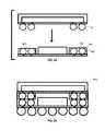
- FIGS. 11-13illustrate stages in a method of forming a microelectronic package 610 in accordance with the embodiment seen in FIG. 6 .
- a subassembly including a first support element 102can be formed having first connectors 161 projecting above the second surface 103 thereof and an encapsulation 152 surrounding individual first connectors 161 and insulating the first connectors from one another.
- the encapsulation 152may be in form of a square or rectangular frame having width in a direction 178 in the view shown, with a central opening in the frame sized to accommodate the microelectronic element 120 .
- Ends 163 of the first connectors 161are exposed at a surface 153 of the encapsulation 152 , and may project above the surface 153 in direction 180 towards the second support element 104 , or may be flush with the surface 153 , or may be recessed below the surface 153 in a direction towards surface 103 of the first support element.
- subassembly 21can be formed by forming a structure of the first support element 102 and first connectors 161 projecting above the second surface 103 thereof.
- First connectors 161may be conductive masses, or can be other first connectors as described relative to other embodiments above.
- An encapsulationcan then be molded onto the structure such as by injecting an encapsulant into a mold therefor, while a plate of the mold rests against ends 163 of the first connectors 161 such that ends 163 may remain uncovered or not fully covered by the encapsulant. Subsequent deflashing may be used to further uncover the ends of the molded first connectors.
- the mold platecan include mold chases sized to accommodate end portions of the first connectors near the ends 163 thereof such that the encapsulant flows around the end portions of the first connectors, and the ends 163 of the first connectors of the resultant subassembly 21 extend above the surface 153 of the molded encapsulation.
- the mold platecan include protrusions at locations aligned with the first connectors so that the first connectors in the resulting subassembly 21 become recessed below the surface 153 of the molded encapsulation.
- the encapsulation 152can include or consist essentially of a polymeric material.
- materials of which the encapsulation can be madeare a potting compound, epoxies, liquid crystal polymers, thermoplastics, and thermoset polymers.
- the encapsulationcan include a polymeric matrix and particulate loading material within the polymeric matrix, such as formed by molding or otherwise depositing an uncured polymeric material which has the particulate loading material therein onto the second surface 103 of the first support element 102 .
- the particulate loading materialmay optionally have a low coefficient of thermal expansion (“CTE”), such that the resulting encapsulation 152 may have a CTE lower than 10 parts per million per degree Celsius hereinafter, “ppm/° C.”.
- the encapsulationmay include a filler material such as glass or ceramic dielectric filler or semiconductor filler among others.
- the subassembly 21then can be moved into position for joining with corresponding second connectors 162 attached to second support element 104 of a second subassembly 22 .
- the first and second connectorscan be aligned with one another and the first and second support elements can be brought to conditions sufficient for a bond metal included in at least one of the first connectors and the second connectors to flow and form joints between the first connectors and the second connectors.
- the first connectorscan be brought into contact with the aligned second connectors before or during an interval in which a temperature of the first connectors, second connectors or both is raised to a temperature at which the bond metal flows.
- an encapsulant 650can be applied to cover the joined first and second connectors 161 , 162 , such as, for example, by molding an encapsulant material such as a flowable overmold material onto the second surface 103 of the first support element 102 and to fill spaces between the first and second support elements 102 , 104 and between microelectronic element and the surface 103 of the support element 102 adjacent thereto.
- an encapsulant materialsuch as a flowable overmold material
- an assembly or package 610is formed such as further described above relative to FIG. 6 .
- second connectors 162can be joined with ends 163 of the first connectors 161 exposed at surface 153 of the second encapsulation. Then, the second connectors 162 can be joined with electrically conductive elements 166 , e.g., pads, posts, or other electrically conductive connectors, at the second surface 106 of the second support element to form an assembly such as or similar to the assembly seen in FIG. 12 . Then, the encapsulant 650 can be applied to the assembly to form an assembly 610 as seen in FIG. 13 and as further described above relative to FIG. 6 .
- the methods described above relative to FIGS. 11-14can be used with any of the types of first connectors and second connectors which are described above relative to FIGS. 1A-B , 2 , 4 A-B, 5 , 6 , and 7 , without limitation.
- the processes of forming one or more of the encapsulations or for forming any or all of the first connectors and/or second connectors and terminalsmay be as further shown and described in U.S. application Ser. No. 11/166,982 (Tessera 3.0-358 CIP); Ser. No. 11/717,587 (Tessera 3.0-358 CIP); Ser. No.
- FIGS. 15-17illustrate stages in a method of forming a microelectronic package 910 in accordance with the embodiment seen in FIG. 9 .
- second connectors 162 on the second support element 103are partially encapsulated within second encapsulation 952 prior to the second connectors 162 being joined with respective first connectors 161 to form an assembly as seen in FIG. 16 .
- an encapsulation 950can be applied to form an assembly 910 as seen in FIG. 17 and as described above relative to FIG. 9 , where encapsulation 950 can contact surfaces 953 , 954 of the second encapsulation 952 and second surfaces 103 , 106 of the first and second support elements 102 , 104 .
- FIG. 18illustrates a variation of the method described above relative to FIGS. 15-17 in which connectors 165 can be joined with ends 164 of the second connectors 162 exposed at surface 953 of the second encapsulant. Then, the connectors 165 can be joined with electrically conductive elements 266 , e.g., pads, posts, or other electrically conductive connectors, at the second surface 103 of the first support element 102 to form an assembly such as or similar to the assembly seen in FIG. 16 . Then, an encapsulant 950 can be applied to the assembly to form an assembly 910 as seen in FIG. 17 and as described above relative to FIG. 9 .
- electrically conductive elements 266e.g., pads, posts, or other electrically conductive connectors
- FIG. 19illustrates an assembly 1110 according to an example in which first support element 102 includes an opening 155 extending between the first and second surfaces 101 , 103 thereof.
- openingcan be used as a port through which an encapsulant can be supplied into an interior space between the first and second support elements when manufacturing the assembly 1110 .
- FIG. 20illustrates an assembly 1210 according to a variation of the embodiment described relative to FIGS. 9 and 17 above in which encapsulation 1252 includes an additional portion overlying the microelectronic element 120 .
- encapsulant 1252is formed as a monolithic region partially encapsulating second connectors 162 and extending onto a major surface 129 and edge surfaces 127 of the microelectronic element.
- Major surface 129can be a front face as described above relative to FIG. 1A when the microelectronic element is mounted face-up on second support element 104 .
- major surface 128can be a rear face of the microelectronic element 120 opposite from the front face when the microelectronic element faces toward the second support element 104 .
- encapsulation 1250can be formed in contact with the encapsulation 1252 and can overlie or be in contact with second surface 103 of first support element 102 .
- FIGS. 21-22depict processing according to a variation of the method described above relative to FIGS. 11-13 .
- subassembly 321can itself be a microelectronic package in which a microelectronic element 130 has contacts electrically coupled to a support element 302 thereof, in similar fashion to the coupling between microelectronic element 20 and support element 104 as described above relative to FIG. 1A .
- an encapsulation 352may cover edge surfaces 132 of the microelectronic element 130 , and may in some cases cover a major surface 134 of the microelectronic element which faces away from the support element 302 of subassembly 321 .
- the connectors 161 of subassembly 321can be aligned and joined with corresponding connectors 162 of the second subassembly 22 and an encapsulation 650 can be formed in spaces between microelectronic element 120 and subassembly 321 to form a multi-level stacked and electrically coupled assembly 1310 which includes the microelectronic elements 120 , 130 , the support elements 302 , 104 to which they are coupled, such that microelectronic elements 120 , 130 can be electrically coupled with one another through the support elements 104 , 302 and the first and second connectors 161 , 162 .
- Joining elements 146e.g., solder balls, such as described above relative to FIG. 3 , can be applied to terminals 142 of support element 104 , typically after forming encapsulation 650 .
- FIG. 23illustrates a variation thereof, similar to that shown in FIG. 14 , in which the process of assembling the first and second subassemblies is carried out with second connectors 162 already attached to ends 163 of first connectors.
- FIG. 24illustrates that in a variation similar to that shown in FIGS. 15-17 above, the assembling process can be carried in a state in which encapsulation 952 partially covers second connectors 162 and in which first connectors 161 are joined with ends 164 of the second connectors 162 which are exposed at surface 953 of the encapsulation 952 .
- FIG. 25illustrates a resulting assembly 1410 formed in this manner.
- FIGS. 26-27illustrate another variation in which both first connectors 161 and second connectors 162 in respective subassemblies can be partially encapsulated as discussed above with respect to the methods shown in FIGS. 11-13 , and 15 - 17 .
- third connectors 169which may be in form of electrically conductive masses such as described above, can be attached and electrically coupled with ends 163 of the first connectors as shown.
- ends 163 of the first connectorsas shown.
- the third connectors 169can be aligned with and joined with the second connectors 162 , and the resulting assembly 1510 can then be encapsulated in a third encapsulation 1550 filling spaces between individual third connectors 169 and filling spaces between microelectronic element 120 and support element 302 .
- the assembly 1510may also be formed with joining elements 146 attached to support element 104 for further connection with corresponding contacts of an external component as described above.
- FIGS. 28-30illustrate processing according to another variation of the methods described above.
- the partial encapsulation on first connectors or on second connectors or on bothcan be omitted.
- a dielectric reinforcing collars 156may be present around individual ones of the first connectors 161 , second connectors 162 , or both.
- the reinforcing collars 156include portions 157 overlying outer surfaces of respective individual connectors, e.g., generally spherical surfaces of conductive masses, or alternatively walls of adjacent posts or other connectors, and the reinforcing collars may form troughs 159 where adjacent reinforcing collars meet.
- the reinforcing collarscan be formed by flowing a material onto a surface 103 of the support element 102 , which may then flow to locations on the surface 103 at which first connectors 161 are attached.
- a dielectric reinforcing materialcan be dispensed as a liquid which flows to areas surrounding individual ones of the first connectors.
- a vacuum application, roller coat, spray-coat, dispensing or screening processmay be used with a liquid material in forming a part or all of the reinforcing collars.
- the dielectric reinforcing materialmay wick up around the connectors so as to support exterior surfaces of the connectors while leaving their ends 163 exposed, and to prevent or substantially prevent collapse of the connectors reinforced thereby when such connectors are joined with other connectors to form the assemblies or packages described herein.
- a deflashing proceduremay in some cases be employed to remove relatively small amounts of the reinforcing material overlying ends 163 .
- such reinforcing material 156can be present at and around second connectors 162 as well. Alternatively, the reinforcing layer can be omitted, as seen in the case of second connectors 162 b .
- the reinforcing materialcan be or include an epoxy material such as an underfill material having a dielectric particulate loading material, such as commonly dispensed to an interface between a contact-bearing face of a microelectronic element such as a semiconductor chip and a surface of a substrate to which the chip is flip-chip attached and electrically interconnected.
- the reinforcing collarsmay in some cases reduce the CTE of the subassembly over which it is applied.
- subassemblies having first and second connectors with ends therein exposedcan be joined together in a manner similar to that described above.
- the joined subassembliescan be mechanically reinforced with an encapsulation 150 filling in spaces between the subassemblies and further reinforcing the joints between first and second connectors.
- the joined first and second connectors 161 , 162can provide increased height and increased aspect ratio of connections between the first and second support elements, in a manner similar to that describe for the foregoing embodiments.
- the stiffening layermay overlie walls of only the second connectors or may overlie walls of only some of the second connectors.
- the first connectors, the second connectors or both the first and second connectorsmay be conductive masses or may be any of the types of connectors shown and discussed in the foregoing.
- a microelectronic packagesuch as the package 321 shown and described above in FIG. 21 can be substituted for the subassembly in FIG. 28 which includes support element 102 and such subassembly can be joined with another microelectronic package to form an assembly similar to that depicted in FIG. 29 .
- any of the assembling processes depicted in FIG. 11-14 , 15 - 18 or 21 - 30can be carried out in a state in which one or both of the subassemblies having microelectronic elements or support elements as described therein is replaced by different structure.
- one or both of the subassembliescan be or can include a multi-level stacked and electrically interconnected assembly of microelectronic elements and support elements coupled to respective microelectronic elements at each level of such subassembly.
- a system 500 in accordance with a further embodiment of the inventionincludes a structure 506 as described above in conjunction with other electronic components 508 and 510 .
- component 508is a semiconductor chip whereas component 510 is a display screen, but any other components can be used.
- the structure 506 as described abovemay be, for example, a microelectronic package as discussed above in the foregoing or may be a microelectronic assembly such as discussed above with respect to FIG. 3 , or FIG. 8 .
- Structure 506 and components 508 and 510are mounted in a common housing 501 , schematically depicted in broken lines, and are electrically interconnected with one another as necessary to form the desired circuit.
- the systemincludes a circuit panel 502 such as a flexible printed circuit board, and the circuit panel includes numerous conductors 504 , of which only one is depicted in FIG. 21 , interconnecting the components with one another.
- the housing 501is depicted as a portable housing of the type usable, for example, in a cellular telephone or personal digital assistant, and screen 510 is exposed at the surface of the housing.
- structure 506includes a light-sensitive element such as an imaging chip
- a lens 511 or other optical devicealso may be provided for routing light to the structure.
- the simplified system shown in FIG. 21is merely exemplary; other systems, including systems commonly regarded as fixed structures, such as desktop computers, routers and the like can be made using the structures discussed above.
Landscapes
- Engineering & Computer Science (AREA)
- Microelectronics & Electronic Packaging (AREA)
- Power Engineering (AREA)
- Physics & Mathematics (AREA)
- Condensed Matter Physics & Semiconductors (AREA)
- General Physics & Mathematics (AREA)
- Computer Hardware Design (AREA)
- Manufacturing & Machinery (AREA)
- Wire Bonding (AREA)
Abstract
Description
Claims (20)
Priority Applications (10)
| Application Number | Priority Date | Filing Date | Title |
|---|---|---|---|
| US13/942,568US9023691B2 (en) | 2013-07-15 | 2013-07-15 | Microelectronic assemblies with stack terminals coupled by connectors extending through encapsulation |
| US14/230,521US8883563B1 (en) | 2013-07-15 | 2014-03-31 | Fabrication of microelectronic assemblies having stack terminals coupled by connectors extending through encapsulation |
| JP2016527027AJP2016529703A (en) | 2013-07-15 | 2014-07-15 | Microelectronic assembly having stacked terminals joined by connectors extending through the seal |
| TW103124236ATWI550736B (en) | 2013-07-15 | 2014-07-15 | Microelectronic assemblies with stack terminals coupled by connectors extending through encapsulation |
| PCT/US2014/046661WO2015009702A1 (en) | 2013-07-15 | 2014-07-15 | Microelectronic assemblies with stack terminals coupled by connectors extending through encapsulation |
| KR1020167003549AKR20160031523A (en) | 2013-07-15 | 2014-07-15 | Microelectronic assemblies with stack terminals coupled by connectors extending through encapsulation |
| CN201480050592.6ACN105556662A (en) | 2013-07-15 | 2014-07-15 | Microelectronic assembly having stacked terminals coupled by connectors extending through encapsulation |
| US14/995,726US9633979B2 (en) | 2013-07-15 | 2016-01-14 | Microelectronic assemblies having stack terminals coupled by connectors extending through encapsulation |
| PCT/US2016/068133WO2017123398A1 (en) | 2013-07-15 | 2016-12-21 | Microelectronic assemblies with stack terminals coupled by connectors extending through encapsulation |
| TW106100602ATW201801285A (en) | 2013-07-15 | 2017-01-09 | Microelectronic assemblies having stack terminals coupled by connectors extending through encapsulation |
Applications Claiming Priority (1)
| Application Number | Priority Date | Filing Date | Title |
|---|---|---|---|
| US13/942,568US9023691B2 (en) | 2013-07-15 | 2013-07-15 | Microelectronic assemblies with stack terminals coupled by connectors extending through encapsulation |
Related Parent Applications (2)
| Application Number | Title | Priority Date | Filing Date |
|---|---|---|---|
| US13/942,602ContinuationUS9034696B2 (en) | 2013-07-15 | 2013-07-15 | Microelectronic assemblies having reinforcing collars on connectors extending through encapsulation |
| PCT/US2014/046661Continuation-In-PartWO2015009702A1 (en) | 2013-07-15 | 2014-07-15 | Microelectronic assemblies with stack terminals coupled by connectors extending through encapsulation |
Related Child Applications (2)
| Application Number | Title | Priority Date | Filing Date |
|---|---|---|---|
| US14/230,521Continuation-In-PartUS8883563B1 (en) | 2013-07-15 | 2014-03-31 | Fabrication of microelectronic assemblies having stack terminals coupled by connectors extending through encapsulation |
| PCT/US2014/046661ContinuationWO2015009702A1 (en) | 2013-07-15 | 2014-07-15 | Microelectronic assemblies with stack terminals coupled by connectors extending through encapsulation |
Publications (2)
| Publication Number | Publication Date |
|---|---|
| US20150014847A1 US20150014847A1 (en) | 2015-01-15 |
| US9023691B2true US9023691B2 (en) | 2015-05-05 |
Family
ID=52276488
Family Applications (1)
| Application Number | Title | Priority Date | Filing Date |
|---|---|---|---|
| US13/942,568ActiveUS9023691B2 (en) | 2013-07-15 | 2013-07-15 | Microelectronic assemblies with stack terminals coupled by connectors extending through encapsulation |
Country Status (1)
| Country | Link |
|---|---|
| US (1) | US9023691B2 (en) |
Cited By (5)
| Publication number | Priority date | Publication date | Assignee | Title |
|---|---|---|---|---|
| US9633979B2 (en)* | 2013-07-15 | 2017-04-25 | Invensas Corporation | Microelectronic assemblies having stack terminals coupled by connectors extending through encapsulation |
| US9812433B2 (en) | 2014-03-31 | 2017-11-07 | Invensas Corporation | Batch process fabrication of package-on-package microelectronic assemblies |
| US10424525B2 (en) | 2017-05-23 | 2019-09-24 | Stmicroelectronics S.R.L. | Method of manufacturing semiconductor devices |
| US10522505B2 (en)* | 2017-04-06 | 2019-12-31 | Advanced Semiconductor Engineering, Inc. | Semiconductor device package and method for manufacturing the same |
| US20200100387A1 (en)* | 2018-09-25 | 2020-03-26 | Apple Inc. | Housing construction |
Families Citing this family (5)
| Publication number | Priority date | Publication date | Assignee | Title |
|---|---|---|---|---|
| US9543277B1 (en)* | 2015-08-20 | 2017-01-10 | Invensas Corporation | Wafer level packages with mechanically decoupled fan-in and fan-out areas |
| WO2017095094A2 (en)* | 2015-11-30 | 2017-06-08 | 하나마이크론(주) | Metal core solder ball interconnector fan-out wafer level package and manufacturing method therefor |
| US9705302B1 (en) | 2015-12-28 | 2017-07-11 | X Development Llc | Combined electrical and mechanical potted termination for a center strength member cable |
| US11239587B2 (en)* | 2018-03-07 | 2022-02-01 | Xcelsis Corporation | Configurable smart object system with clip-based connectors |
| US10497657B1 (en) | 2018-06-13 | 2019-12-03 | Advanced Semiconductor Engineering, Inc. | Semiconductor package device and method of manufacturing the same |
Citations (367)
| Publication number | Priority date | Publication date | Assignee | Title |
|---|---|---|---|---|
| US3289452A (en) | 1963-07-23 | 1966-12-06 | Siemens Ag | Method and device for bonding a contact wire to a semiconductor member |
| US3358897A (en) | 1964-03-31 | 1967-12-19 | Tempress Res Co | Electric lead wire bonding tools |
| US3623649A (en) | 1969-06-09 | 1971-11-30 | Gen Motors Corp | Wedge bonding tool for the attachment of semiconductor leads |
| US3795037A (en) | 1970-05-05 | 1974-03-05 | Int Computers Ltd | Electrical connector devices |
| US3900153A (en) | 1972-06-13 | 1975-08-19 | Licentia Gmbh | Formation of solder layers |
| US4327860A (en) | 1980-01-03 | 1982-05-04 | Kulicke And Soffa Ind. Inc. | Method of making slack free wire interconnections |
| US4422568A (en) | 1981-01-12 | 1983-12-27 | Kulicke And Soffa Industries, Inc. | Method of making constant bonding wire tail lengths |
| US4437604A (en) | 1982-03-15 | 1984-03-20 | Kulicke & Soffa Industries, Inc. | Method of making fine wire interconnections |
| JPS61125062A (en) | 1984-11-22 | 1986-06-12 | Hitachi Ltd | Method and device for attaching pin |
| US4604644A (en) | 1985-01-28 | 1986-08-05 | International Business Machines Corporation | Solder interconnection structure for joining semiconductor devices to substrates that have improved fatigue life, and process for making |
| US4695870A (en) | 1986-03-27 | 1987-09-22 | Hughes Aircraft Company | Inverted chip carrier |
| JPS62226307A (en) | 1986-03-28 | 1987-10-05 | Toshiba Corp | robot equipment |
| US4716049A (en) | 1985-12-20 | 1987-12-29 | Hughes Aircraft Company | Compressive pedestal for microminiature connections |
| US4771930A (en) | 1986-06-30 | 1988-09-20 | Kulicke And Soffa Industries Inc. | Apparatus for supplying uniform tail lengths |
| US4793814A (en) | 1986-07-21 | 1988-12-27 | Rogers Corporation | Electrical circuit board interconnect |
| US4804132A (en) | 1987-08-28 | 1989-02-14 | Difrancesco Louis | Method for cold bonding |
| JPS6471162A (en) | 1987-09-11 | 1989-03-16 | Hitachi Ltd | Semiconductor device |
| US4902600A (en) | 1986-10-14 | 1990-02-20 | Fuji Photo Film Co., Ltd. | Light-sensitive material comprising light-sensitive layer provided on support wherein the light-sensitive layer and support have specified pH values |
| US4924353A (en) | 1985-12-20 | 1990-05-08 | Hughes Aircraft Company | Connector system for coupling to an integrated circuit chip |
| US4975079A (en) | 1990-02-23 | 1990-12-04 | International Business Machines Corp. | Connector assembly for chip testing |
| US4982265A (en) | 1987-06-24 | 1991-01-01 | Hitachi, Ltd. | Semiconductor integrated circuit device and method of manufacturing the same |
| US4998885A (en) | 1989-10-27 | 1991-03-12 | International Business Machines Corporation | Elastomeric area array interposer |
| US4999472A (en) | 1990-03-12 | 1991-03-12 | Neinast James E | Electric arc system for ablating a surface coating |
| US5067382A (en) | 1990-11-02 | 1991-11-26 | Cray Computer Corporation | Method and apparatus for notching a lead wire attached to an IC chip to facilitate severing the wire |
| US5083697A (en) | 1990-02-14 | 1992-01-28 | Difrancesco Louis | Particle-enhanced joining of metal surfaces |
| US5095187A (en) | 1989-12-20 | 1992-03-10 | Raychem Corporation | Weakening wire supplied through a wire bonder |
| US5138438A (en) | 1987-06-24 | 1992-08-11 | Akita Electronics Co. Ltd. | Lead connections means for stacked tab packaged IC chips |
| US5148265A (en) | 1990-09-24 | 1992-09-15 | Ist Associates, Inc. | Semiconductor chip assemblies with fan-in leads |
| US5148266A (en) | 1990-09-24 | 1992-09-15 | Ist Associates, Inc. | Semiconductor chip assemblies having interposer and flexible lead |
| US5186381A (en) | 1991-04-16 | 1993-02-16 | Samsung Electronics, Co., Ltd. | Semiconductor chip bonding process |
| US5189505A (en) | 1989-11-08 | 1993-02-23 | Hewlett-Packard Company | Flexible attachment flip-chip assembly |
| US5196726A (en) | 1990-01-23 | 1993-03-23 | Sumitomo Electric Industries, Ltd. | Substrate for packaging a semiconductor device having particular terminal and bump structure |
| US5214308A (en) | 1990-01-23 | 1993-05-25 | Sumitomo Electric Industries, Ltd. | Substrate for packaging a semiconductor device |
| US5220489A (en) | 1991-10-11 | 1993-06-15 | Motorola, Inc. | Multicomponent integrated circuit package |
| US5222014A (en) | 1992-03-02 | 1993-06-22 | Motorola, Inc. | Three-dimensional multi-chip pad array carrier |
| US5340771A (en) | 1993-03-18 | 1994-08-23 | Lsi Logic Corporation | Techniques for providing high I/O count connections to semiconductor dies |
| JPH06268015A (en) | 1993-03-10 | 1994-09-22 | Nec Corp | Integrated circuit |
| US5371654A (en) | 1992-10-19 | 1994-12-06 | International Business Machines Corporation | Three dimensional high performance interconnection package |
| US5397997A (en) | 1991-08-23 | 1995-03-14 | Nchip, Inc. | Burn-in technologies for unpackaged integrated circuits |
| JPH07122787A (en) | 1993-09-06 | 1995-05-12 | Sharp Corp | Structure of chip component type LED and manufacturing method thereof |
| US5438224A (en) | 1992-04-23 | 1995-08-01 | Motorola, Inc. | Integrated circuit package having a face-to-face IC chip arrangement |
| US5455390A (en) | 1994-02-01 | 1995-10-03 | Tessera, Inc. | Microelectronics unit mounting with multiple lead bonding |
| US5468995A (en) | 1994-07-05 | 1995-11-21 | Motorola, Inc. | Semiconductor device having compliant columnar electrical connections |
| US5494667A (en) | 1992-06-04 | 1996-02-27 | Kabushiki Kaisha Hayahibara | Topically applied hair restorer containing pine extract |
| US5495667A (en) | 1994-11-07 | 1996-03-05 | Micron Technology, Inc. | Method for forming contact pins for semiconductor dice and interconnects |
| US5518964A (en) | 1994-07-07 | 1996-05-21 | Tessera, Inc. | Microelectronic mounting with multiple lead deformation and bonding |
| US5536909A (en) | 1992-07-24 | 1996-07-16 | Tessera, Inc. | Semiconductor connection components and methods with releasable lead support |
| US5541567A (en) | 1994-10-17 | 1996-07-30 | International Business Machines Corporation | Coaxial vias in an electronic substrate |
| US5571428A (en) | 1992-01-17 | 1996-11-05 | Hitachi, Ltd. | Semiconductor leadframe and its production method and plastic encapsulated semiconductor device |
| US5608265A (en) | 1993-03-17 | 1997-03-04 | Hitachi, Ltd. | Encapsulated semiconductor device package having holes for electrically conductive material |
| US5615824A (en) | 1994-06-07 | 1997-04-01 | Tessera, Inc. | Soldering with resilient contacts |
| US5656550A (en) | 1994-08-24 | 1997-08-12 | Fujitsu Limited | Method of producing a semicondutor device having a lead portion with outer connecting terminal |
| US5659952A (en) | 1994-09-20 | 1997-08-26 | Tessera, Inc. | Method of fabricating compliant interface for semiconductor chip |
| US5679977A (en) | 1990-09-24 | 1997-10-21 | Tessera, Inc. | Semiconductor chip assemblies, methods of making same and components for same |
| US5688716A (en) | 1994-07-07 | 1997-11-18 | Tessera, Inc. | Fan-out semiconductor chip assembly |
| US5726493A (en) | 1994-06-13 | 1998-03-10 | Fujitsu Limited | Semiconductor device and semiconductor device unit having ball-grid-array type package structure |
| US5731709A (en) | 1996-01-26 | 1998-03-24 | Motorola, Inc. | Method for testing a ball grid array semiconductor device and a device for such testing |
| US5736780A (en) | 1995-11-07 | 1998-04-07 | Shinko Electric Industries Co., Ltd. | Semiconductor device having circuit pattern along outer periphery of sealing resin and related processes |
| US5802699A (en) | 1994-06-07 | 1998-09-08 | Tessera, Inc. | Methods of assembling microelectronic assembly with socket for engaging bump leads |
| US5811982A (en) | 1995-11-27 | 1998-09-22 | International Business Machines Corporation | High density cantilevered probe for electronic devices |
| US5831836A (en) | 1992-01-30 | 1998-11-03 | Lsi Logic | Power plane for semiconductor device |
| US5854507A (en) | 1998-07-21 | 1998-12-29 | Hewlett-Packard Company | Multiple chip assembly |
| JPH1174295A (en) | 1997-08-29 | 1999-03-16 | Citizen Electron Co Ltd | Method for packaging electronic circuit |
| US5898991A (en) | 1997-01-16 | 1999-05-04 | International Business Machines Corporation | Methods of fabrication of coaxial vias and magnetic devices |
| JPH11135663A (en) | 1997-10-28 | 1999-05-21 | Nec Kyushu Ltd | Molded bga type semiconductor device and manufacture thereof |
| US5912505A (en) | 1995-11-07 | 1999-06-15 | Sumitomo Metal (Smi) Electronics Devices, Inc. | Semiconductor package and semiconductor device |
| US5953624A (en) | 1997-01-13 | 1999-09-14 | Kabushiki Kaisha Shinkawa | Bump forming method |
| JPH11251350A (en) | 1998-02-27 | 1999-09-17 | Fuji Xerox Co Ltd | Method and apparatus for forming bump |
| US5973391A (en) | 1997-12-11 | 1999-10-26 | Read-Rite Corporation | Interposer with embedded circuitry and method for using the same to package microelectronic units |
| US5971253A (en) | 1995-07-31 | 1999-10-26 | Tessera, Inc. | Microelectronic component mounting with deformable shell terminals |
| US5977618A (en) | 1992-07-24 | 1999-11-02 | Tessera, Inc. | Semiconductor connection components and methods with releasable lead support |
| US5989936A (en) | 1994-07-07 | 1999-11-23 | Tessera, Inc. | Microelectronic assembly fabrication with terminal formation from a conductive layer |
| US5994152A (en) | 1996-02-21 | 1999-11-30 | Formfactor, Inc. | Fabricating interconnects and tips using sacrificial substrates |
| US6002168A (en) | 1997-11-25 | 1999-12-14 | Tessera, Inc. | Microelectronic component with rigid interposer |
| US6032359A (en) | 1997-08-21 | 2000-03-07 | Carroll; Keith C. | Method of manufacturing a female electrical connector in a single layer flexible polymeric dielectric film substrate |
| US6038136A (en) | 1997-10-29 | 2000-03-14 | Hestia Technologies, Inc. | Chip package with molded underfill |
| US6052287A (en) | 1997-12-09 | 2000-04-18 | Sandia Corporation | Silicon ball grid array chip carrier |
| US6054756A (en) | 1992-07-24 | 2000-04-25 | Tessera, Inc. | Connection components with frangible leads and bus |
| US6054337A (en) | 1996-12-13 | 2000-04-25 | Tessera, Inc. | Method of making a compliant multichip package |
| US6077380A (en) | 1995-06-30 | 2000-06-20 | Microfab Technologies, Inc. | Method of forming an adhesive connection |
| US6117694A (en) | 1994-07-07 | 2000-09-12 | Tessera, Inc. | Flexible lead structures and methods of making same |
| KR100265563B1 (en) | 1998-06-29 | 2000-09-15 | 김영환 | Ball grid array package and fabricating method thereof |
| US6121676A (en) | 1996-12-13 | 2000-09-19 | Tessera, Inc. | Stacked microelectronic assembly and method therefor |
| US6124546A (en) | 1997-12-03 | 2000-09-26 | Advanced Micro Devices, Inc. | Integrated circuit chip package and method of making the same |
| US6133072A (en) | 1996-12-13 | 2000-10-17 | Tessera, Inc. | Microelectronic connector with planar elastomer sockets |
| US6157080A (en) | 1997-11-06 | 2000-12-05 | Sharp Kabushiki Kaisha | Semiconductor device using a chip scale package |
| US6158647A (en) | 1998-09-29 | 2000-12-12 | Micron Technology, Inc. | Concave face wire bond capillary |
| US6164523A (en) | 1998-07-01 | 2000-12-26 | Semiconductor Components Industries, Llc | Electronic component and method of manufacture |
| US6177636B1 (en) | 1994-12-29 | 2001-01-23 | Tessera, Inc. | Connection components with posts |
| US6194250B1 (en) | 1998-09-14 | 2001-02-27 | Motorola, Inc. | Low-profile microelectronic package |
| US6202297B1 (en) | 1995-08-28 | 2001-03-20 | Tessera, Inc. | Socket for engaging bump leads on a microelectronic device and methods therefor |
| US6202298B1 (en) | 1996-05-02 | 2001-03-20 | Tessera, Inc. | Microelectronic connections with liquid conductive elements |
| US6206273B1 (en) | 1999-02-17 | 2001-03-27 | International Business Machines Corporation | Structures and processes to create a desired probetip contact geometry on a wafer test probe |
| US6208024B1 (en) | 1996-12-12 | 2001-03-27 | Tessera, Inc. | Microelectronic mounting with multiple lead deformation using restraining straps |
| US6211572B1 (en) | 1995-10-31 | 2001-04-03 | Tessera, Inc. | Semiconductor chip package with fan-in leads |
| US6215670B1 (en) | 1993-11-16 | 2001-04-10 | Formfactor, Inc. | Method for manufacturing raised electrical contact pattern of controlled geometry |
| US6225688B1 (en) | 1997-12-11 | 2001-05-01 | Tessera, Inc. | Stacked microelectronic assembly and method therefor |
| US20010002607A1 (en) | 1999-12-02 | 2001-06-07 | Kazuo Sugiura | Method for forming pin-form wires and the like |
| US6258625B1 (en) | 1999-05-18 | 2001-07-10 | International Business Machines Corporation | Method of interconnecting electronic components using a plurality of conductive studs |
| US6260264B1 (en) | 1997-12-08 | 2001-07-17 | 3M Innovative Properties Company | Methods for making z-axis electrical connections |
| US6262482B1 (en) | 1998-02-03 | 2001-07-17 | Oki Electric Industry Co., Ltd. | Semiconductor device |
| JP2001196407A (en) | 2000-01-14 | 2001-07-19 | Seiko Instruments Inc | Semiconductor device and method of forming the same |
| US20010021541A1 (en) | 1999-06-28 | 2001-09-13 | Salman Akram | Wafer-level package and methods of fabricating |
| US6295729B1 (en) | 1992-10-19 | 2001-10-02 | International Business Machines Corporation | Angled flying lead wire bonding process |
| US20010028114A1 (en) | 2000-03-27 | 2001-10-11 | Kabushiki Kaisha Toshiba | Semiconductor device including memory unit and semiconductor module including memory units |
| US6303997B1 (en) | 1998-04-08 | 2001-10-16 | Anam Semiconductor, Inc. | Thin, stackable semiconductor packages |
| KR20010094894A (en) | 2000-04-07 | 2001-11-03 | 마이클 디. 오브라이언 | Semiconductor package and its manufacturing method |
| US6316838B1 (en) | 1999-10-29 | 2001-11-13 | Fujitsu Limited | Semiconductor device |
| US6332270B2 (en) | 1998-11-23 | 2001-12-25 | International Business Machines Corporation | Method of making high density integral test probe |
| WO2002013256A1 (en) | 2000-08-08 | 2002-02-14 | Telefonaktiebolaget Lm Ericsson (Publ) | Method of securing solder balls and any components fixed to one and the same side of a substrate |
| US6358627B2 (en) | 1999-04-03 | 2002-03-19 | International Business Machines Corporation | Rolling ball connector |
| US6362525B1 (en) | 1999-11-09 | 2002-03-26 | Cypress Semiconductor Corp. | Circuit structure including a passive element formed within a grid array substrate and method for making the same |
| US6388333B1 (en) | 1999-11-30 | 2002-05-14 | Fujitsu Limited | Semiconductor device having protruding electrodes higher than a sealed portion |
| US20020066952A1 (en) | 2000-12-04 | 2002-06-06 | Fujitsu Limited | Semiconductor device having an interconnecting post formed on an interposer within a sealing resin |
| US6407448B2 (en) | 1998-05-30 | 2002-06-18 | Hyundai Electronics Industries Co., Inc. | Stackable ball grid array semiconductor package and fabrication method thereof |
| KR20020058216A (en) | 2000-12-29 | 2002-07-12 | 마이클 디. 오브라이언 | Stacked semiconductor package and its manufacturing method |
| US20020117330A1 (en) | 1993-11-16 | 2002-08-29 | Formfactor, Inc. | Resilient contact structures formed and then attached to a substrate |
| US20020125571A1 (en) | 1998-06-30 | 2002-09-12 | Corisis David J. | Module assembly for stacked BGA packages |
| US6458411B1 (en) | 2001-01-17 | 2002-10-01 | Aralight, Inc. | Method of making a mechanically compliant bump |
| JP2002289769A (en) | 2001-03-26 | 2002-10-04 | Matsushita Electric Ind Co Ltd | Stacked semiconductor device and method of manufacturing the same |
| US20020153602A1 (en) | 2000-05-16 | 2002-10-24 | Tay Wuu Yean | Ball grid array chip packages having improved testing and stacking characteristics |
| US6476583B2 (en) | 2000-07-21 | 2002-11-05 | Jomahip, Llc | Automatic battery charging system for a battery back-up DC power supply |
| US6476503B1 (en) | 1999-08-12 | 2002-11-05 | Fujitsu Limited | Semiconductor device having columnar electrode and method of manufacturing same |
| US20020164838A1 (en) | 2001-05-02 | 2002-11-07 | Moon Ow Chee | Flexible ball grid array chip scale packages and methods of fabrication |
| US20020185735A1 (en) | 1998-10-28 | 2002-12-12 | International Business Machines Corporation | Bump connection and method and apparatus for forming said connection |
| US6495914B1 (en) | 1997-08-19 | 2002-12-17 | Hitachi, Ltd. | Multi-chip module structure having conductive blocks to provide electrical connection between conductors on first and second sides of a conductive base substrate |
| US20030006494A1 (en) | 2001-07-03 | 2003-01-09 | Lee Sang Ho | Thin profile stackable semiconductor package and method for manufacturing |
| US6507104B2 (en) | 2000-09-07 | 2003-01-14 | Siliconware Precision Industries Co., Ltd. | Semiconductor package with embedded heat-dissipating device |
| US6509639B1 (en) | 2001-07-27 | 2003-01-21 | Charles W. C. Lin | Three-dimensional stacked semiconductor package |
| US6514847B1 (en) | 1997-11-28 | 2003-02-04 | Sony Corporation | Method for making a semiconductor device |
| US6515355B1 (en) | 1998-09-02 | 2003-02-04 | Micron Technology, Inc. | Passivation layer for packaged integrated circuits |
| US6528874B1 (en) | 1999-10-12 | 2003-03-04 | North Corporation | Wiring circuit substrate and manufacturing method thereof |
| US6531784B1 (en) | 2000-06-02 | 2003-03-11 | Amkor Technology, Inc. | Semiconductor package with spacer strips |
| US20030048108A1 (en) | 1993-04-30 | 2003-03-13 | Beaman Brian Samuel | Structural design and processes to control probe position accuracy in a wafer test probe assembly |
| US20030057544A1 (en) | 2001-09-13 | 2003-03-27 | Nathan Richard J. | Integrated assembly protocol |
| US6545228B2 (en) | 2000-09-05 | 2003-04-08 | Seiko Epson Corporation | Semiconductor device with a plurality of stacked boards and method of making |
| US6550666B2 (en) | 2001-08-21 | 2003-04-22 | Advanpack Solutions Pte Ltd | Method for forming a flip chip on leadframe semiconductor package |
| JP2003122611A (en) | 2001-10-11 | 2003-04-25 | Oki Electric Ind Co Ltd | Data providing method and server device |
| US6555918B2 (en) | 1997-09-29 | 2003-04-29 | Hitachi, Ltd. | Stacked semiconductor device including improved lead frame arrangement |
| US6560117B2 (en) | 2000-06-28 | 2003-05-06 | Micron Technology, Inc. | Packaged microelectronic die assemblies and methods of manufacture |
| US20030094700A1 (en) | 2001-11-16 | 2003-05-22 | Fujitsu Limited | Light signal processing system |
| US6573458B1 (en) | 1998-09-07 | 2003-06-03 | Ngk Spark Plug Co., Ltd. | Printed circuit board |
| US6578755B1 (en) | 2000-09-22 | 2003-06-17 | Flip Chip Technologies, L.L.C. | Polymer collar for solder bumps |
| US6578754B1 (en) | 2000-04-27 | 2003-06-17 | Advanpack Solutions Pte. Ltd. | Pillar connections for semiconductor chips and method of manufacture |
| JP2003174124A (en) | 2001-12-04 | 2003-06-20 | Sainekkusu:Kk | Method for forming external electrode of semiconductor device |
| US20030124767A1 (en) | 2001-12-31 | 2003-07-03 | Jin-Yuan Lee | Integrated chip package structure using ceramic substrate and method of manufacturing the same |
| US6600234B2 (en) | 1999-02-03 | 2003-07-29 | Casio Computer Co., Ltd. | Mounting structure having columnar electrodes and a sealing film |
| US20030162378A1 (en) | 2001-12-28 | 2003-08-28 | Seiko Epson Corporation | Bonding method and bonding apparatus |
| US20030164540A1 (en) | 2002-03-04 | 2003-09-04 | Lee Teck Kheng | Semiconductor die packages with recessed interconnecting structures and methods for assembling the same |
| US6624653B1 (en) | 2000-08-28 | 2003-09-23 | Micron Technology, Inc. | Method and system for wafer level testing and burning-in semiconductor components |
| US6630730B2 (en) | 2000-04-28 | 2003-10-07 | Micron Technology, Inc. | Semiconductor device assemblies including interposers with dams protruding therefrom |
| JP2003307897A (en) | 2001-10-16 | 2003-10-31 | Hokushin Ind Inc | Conductive blade |
| US6647310B1 (en) | 2000-05-30 | 2003-11-11 | Advanced Micro Devices, Inc. | Temperature control of an integrated circuit |
| US6684007B2 (en) | 1998-10-09 | 2004-01-27 | Fujitsu Limited | Optical coupling structures and the fabrication processes |
| US6687988B1 (en) | 1999-10-20 | 2004-02-10 | Kabushiki Kaisha Shinkawa | Method for forming pin-form wires and the like |
| US20040038447A1 (en) | 2002-08-21 | 2004-02-26 | Corisis David J | Packaged microelectronic devices and methods for assembling microelectronic devices |
| US20040036164A1 (en) | 2001-07-31 | 2004-02-26 | Toshihiko Koike | Semiconductor device and its manufacturing method |
| US20040075164A1 (en) | 2002-10-18 | 2004-04-22 | Siliconware Precision Industries, Ltd. | Module device of stacked semiconductor packages and method for fabricating the same |
| US6730544B1 (en) | 1999-12-20 | 2004-05-04 | Amkor Technology, Inc. | Stackable semiconductor package and method for manufacturing same |
| US6734542B2 (en) | 2000-12-27 | 2004-05-11 | Matsushita Electric Industrial Co., Ltd. | Component built-in module and method for producing the same |
| US20040090756A1 (en) | 2002-11-07 | 2004-05-13 | Kwun-Yo Ho | Chip packaging structure and manufacturing process thereof |
| US6746894B2 (en) | 2001-03-30 | 2004-06-08 | Micron Technology, Inc. | Ball grid array interposer, packages and methods |
| US20040110319A1 (en) | 1994-03-18 | 2004-06-10 | Hitachi Chemical Company, Ltd. | Fabrication process of semiconductor package and semiconductor package |
| US20040119152A1 (en) | 2002-10-08 | 2004-06-24 | Chippac, Inc. | Semiconductor multi-package module having inverted bump chip carrier second package |
| US6762078B2 (en) | 1999-05-20 | 2004-07-13 | Amkor Technology, Inc. | Semiconductor package having semiconductor chip within central aperture of substrate |
| US6765287B1 (en) | 2001-07-27 | 2004-07-20 | Charles W. C. Lin | Three-dimensional stacked semiconductor package |
| US20040152292A1 (en) | 2002-09-19 | 2004-08-05 | Stephen Babinetz | Method and apparatus for forming bumps for semiconductor interconnections using a wire bonding machine |
| US6774473B1 (en) | 1999-07-30 | 2004-08-10 | Ming-Tung Shen | Semiconductor chip module |
| US6774494B2 (en) | 2001-03-22 | 2004-08-10 | Renesas Technology Corp. | Semiconductor device and manufacturing method thereof |
| US6774467B2 (en) | 2000-03-24 | 2004-08-10 | Shinko Electric Industries Co., Ltd | Semiconductor device and process of production of same |
| US6777787B2 (en) | 2000-03-28 | 2004-08-17 | Rohm Co., Ltd. | Semiconductor device with warp preventing board joined thereto |
| US20040160751A1 (en) | 1999-09-02 | 2004-08-19 | Ibiden Co., Ltd. | Printed circuit board and method of manufacturing printed circuit board |
| US6790757B1 (en) | 1999-12-20 | 2004-09-14 | Agere Systems Inc. | Wire bonding method for copper interconnects in semiconductor devices |
| US20040188499A1 (en) | 2003-01-14 | 2004-09-30 | Hitoshi Nosaka | Wire bonding method and wire bonding apparatus |
| JP2004281514A (en) | 2003-03-13 | 2004-10-07 | Denso Corp | Wire bonding method |
| US6815257B2 (en) | 2002-03-18 | 2004-11-09 | Samsung Electro-Mechanics Co., Ltd. | Chip scale package and method of fabricating the same |
| JP2004327856A (en) | 2003-04-25 | 2004-11-18 | North:Kk | Method for manufacturing wiring circuit board and method for manufacturing semiconductor integrated circuit device using the wiring circuit board |
| JP2004343030A (en) | 2003-03-31 | 2004-12-02 | North:Kk | Wiring circuit board, manufacturing method thereof, circuit module provided with this wiring circuit board |
| US6828668B2 (en) | 1994-07-07 | 2004-12-07 | Tessera, Inc. | Flexible lead structures and methods of making same |
| US20040262734A1 (en) | 2003-06-30 | 2004-12-30 | Cheol-Joon Yoo | Stack type ball grid array package and method for manufacturing the same |
| JP2005011874A (en) | 2003-06-17 | 2005-01-13 | Matsushita Electric Ind Co Ltd | Semiconductor built-in module and manufacturing method thereof |
| US6844619B2 (en) | 2000-12-01 | 2005-01-18 | Nec Corporation | Compact semiconductor device capable of mounting a plurality of semiconductor chips with high density and method of manufacturing the same |
| US6856235B2 (en) | 1996-04-18 | 2005-02-15 | Tessera, Inc. | Methods for manufacturing resistors using a sacrificial layer |
| US20050035440A1 (en) | 2001-08-22 | 2005-02-17 | Tessera, Inc. | Stacked chip assembly with stiffening layer |
| US6867499B1 (en) | 1999-09-30 | 2005-03-15 | Skyworks Solutions, Inc. | Semiconductor packaging |
| US20050062492A1 (en) | 2001-08-03 | 2005-03-24 | Beaman Brian Samuel | High density integrated circuit apparatus, test probe and methods of use thereof |
| US20050082664A1 (en) | 2003-10-16 | 2005-04-21 | Elpida Memory, Inc. | Stacked semiconductor device and semiconductor chip control method |
| US20050095835A1 (en) | 2003-09-26 | 2005-05-05 | Tessera, Inc. | Structure and method of making capped chips having vertical interconnects |
| US6900530B1 (en) | 2003-12-29 | 2005-05-31 | Ramtek Technology, Inc. | Stacked IC |
| US20050116326A1 (en) | 2003-10-06 | 2005-06-02 | Tessera, Inc. | Formation of circuitry with modification of feature height |
| JP2005142378A (en) | 2003-11-07 | 2005-06-02 | North:Kk | Method for manufacturing member for wiring circuit |
| US6902869B2 (en) | 1997-11-12 | 2005-06-07 | International Business Machines Corporation | Manufacturing methods for printed circuit boards |
| US20050121764A1 (en) | 2003-12-04 | 2005-06-09 | Debendra Mallik | Stackable integrated circuit packaging |
| US20050133916A1 (en) | 2003-12-17 | 2005-06-23 | Stats Chippac, Inc | Multiple chip package module having inverted package stacked over die |
| US20050133932A1 (en) | 2003-12-19 | 2005-06-23 | Jens Pohl | Semiconductor module with a semiconductor stack, and methods for its production |
| US20050140265A1 (en) | 2003-12-26 | 2005-06-30 | Semiconductor Energy Laboratory Co., Ltd. | Display device and method for manufacturing display device |
| JP2005183880A (en) | 2003-12-24 | 2005-07-07 | Fujikura Ltd | SUBSTRATE FOR MULTILAYER WIRING BOARD, DOUBLE WIRE WIRING BOARD AND METHOD FOR PRODUCING THEM |
| US20050151238A1 (en) | 2003-12-29 | 2005-07-14 | Vinu Yamunan | Three-level leadframe for no-lead packages |
| US20050151235A1 (en) | 2004-01-14 | 2005-07-14 | Tetsuya Yokoi | Semiconductor device and manufacturing method for the same |
| US20050173807A1 (en) | 2004-02-05 | 2005-08-11 | Jianbai Zhu | High density vertically stacked semiconductor device |
| US20050173805A1 (en) | 2003-12-30 | 2005-08-11 | Tessera, Inc. | Micro pin grid array with pin motion isolation |
| US6930256B1 (en) | 2002-05-01 | 2005-08-16 | Amkor Technology, Inc. | Integrated circuit substrate having laser-embedded conductive patterns and method therefor |
| US20050181655A1 (en) | 2003-12-30 | 2005-08-18 | Tessera, Inc. | Micro pin grid array with wiping action |
| US20050181544A1 (en) | 2003-12-30 | 2005-08-18 | Tessera, Inc. | Microelectronic packages and methods therefor |
| US6933608B2 (en) | 2002-11-21 | 2005-08-23 | Kaijo Corporation | Wire loop, semiconductor device having same, wire bonding method and wire bonding apparatus |
| US6946380B2 (en) | 2002-02-19 | 2005-09-20 | Seiko Epson Corporation | Method for forming bump, semiconductor element having bumps and method of manufacturing the same, semiconductor device and method of manufacturing the same, circuit board, and electronic equipment |
| US20050212109A1 (en) | 2004-03-23 | 2005-09-29 | Cherukuri Kalyan C | Vertically stacked semiconductor device |
| JP2005302765A (en) | 2004-04-06 | 2005-10-27 | Seiko Epson Corp | SEMICONDUCTOR DEVICE, ITS MANUFACTURING METHOD, AND ELECTRONIC DEVICE |
| US6962864B1 (en) | 2004-05-26 | 2005-11-08 | National Chung Cheng University | Wire-bonding method for chips with copper interconnects by introducing a thin layer |
| US6962282B2 (en) | 2002-03-09 | 2005-11-08 | Fujitsu Limited | System for providing an open-cavity low profile encapsulated semiconductor package |
| US20050253213A1 (en) | 2004-05-13 | 2005-11-17 | Tongbi Jiang | Covers for microelectronic imagers and methods for wafer-level packaging of microelectronics imagers |
| US6979599B2 (en) | 2001-01-10 | 2005-12-27 | Silverbrook Research Pty Ltd | Chip with molded cap array |
| US20050285246A1 (en) | 2004-06-25 | 2005-12-29 | Tessera, Inc. | Microelectronic packages and methods therefor |
| US6987032B1 (en) | 2002-07-19 | 2006-01-17 | Asat Ltd. | Ball grid array package and process for manufacturing same |
| US7009297B1 (en) | 2000-10-13 | 2006-03-07 | Bridge Semiconductor Corporation | Semiconductor chip assembly with embedded metal particle |
| US7045884B2 (en) | 2002-10-04 | 2006-05-16 | International Rectifier Corporation | Semiconductor device package |
| WO2006050691A2 (en) | 2004-11-02 | 2006-05-18 | Imasys Ag | Laying device, contacting device, advancing system, laying and contacting unit, production system, method for the production and a transponder unit |
| US20060118641A1 (en) | 2004-12-08 | 2006-06-08 | Yi-Sung Hwang | Semiconductor device and method of manufacturing the same |
| US7061079B2 (en) | 2003-11-17 | 2006-06-13 | Advanced Semiconductor Engineering, Inc. | Chip package structure and manufacturing method thereof |
| US20060166397A1 (en) | 2002-09-30 | 2006-07-27 | Lau Daniel K | Thermal enhanced package for block mold assembly |
| US7087995B2 (en) | 2002-07-05 | 2006-08-08 | Micron Technology, Inc. | Microelectronic device packages and methods for controlling the disposition of non-conductive materials in such packages |
| US20060197220A1 (en) | 2005-02-15 | 2006-09-07 | Gottfried Beer | Semiconductor device having a plastic housing and external connections and method for producing the same |
| US7119427B2 (en) | 2003-11-13 | 2006-10-10 | Samsung Electronics Ltd., Co. | Stacked BGA packages |
| US20060255449A1 (en) | 2005-05-12 | 2006-11-16 | Yonggill Lee | Lid used in package structure and the package structure having the same |
| US20060278682A1 (en) | 2005-06-09 | 2006-12-14 | Texas Instruments Incorporated | Bond capillary design for ribbon wire bonding |
| US20070015353A1 (en) | 2005-07-14 | 2007-01-18 | Craig David M | Electrically connecting substrate with electrical device |
| US7176559B2 (en) | 2002-08-16 | 2007-02-13 | Via Technologies, Inc. | Integrated circuit package with a balanced-part structure |
| US7176506B2 (en) | 2001-08-28 | 2007-02-13 | Tessera, Inc. | High frequency chip packages with connecting elements |
| US20070040264A1 (en)* | 2002-07-08 | 2007-02-22 | Hall Frank L | Underfilled semiconductor die assemblies and methods of forming the same |
| US7190061B2 (en) | 2003-01-03 | 2007-03-13 | Samsung Electronics Co., Ltd. | stack package made of chip scale packages |
| DE102005051414B3 (en) | 2005-10-25 | 2007-04-12 | Infineon Technologies Ag | Semiconductor component with wiring substrate and solder balls and production processes has central plastic mass and lower film template for lower solder ball arrangement |
| US7215033B2 (en) | 2003-11-19 | 2007-05-08 | Samsung Electronics Co., Ltd. | Wafer level stack structure for system-in-package and method thereof |
| JP2007123595A (en) | 2005-10-28 | 2007-05-17 | Nec Corp | Semiconductor device and its mounting structure |
| US7227095B2 (en) | 2003-08-06 | 2007-06-05 | Micron Technology, Inc. | Wire bonders and methods of wire-bonding |
| US7233057B2 (en) | 2004-05-28 | 2007-06-19 | Nokia Corporation | Integrated circuit package with optimized mold shape |
| US20070148822A1 (en) | 2005-12-23 | 2007-06-28 | Tessera, Inc. | Microelectronic packages and methods therefor |
| US7242081B1 (en) | 2006-04-24 | 2007-07-10 | Advanced Semiconductor Engineering Inc. | Stacked package structure |
| US20070182012A1 (en) | 2004-07-01 | 2007-08-09 | Interuniversitair Microelektronica Centrum (Imec) | Methods for bonding and devices according to such methods |
| US20070181989A1 (en) | 2006-02-08 | 2007-08-09 | Micron Technology, Inc. | Microelectronic devices, stacked microelectronic devices, and methods for manufacturing such devices |
| US20070190747A1 (en) | 2006-01-23 | 2007-08-16 | Tessera Technologies Hungary Kft. | Wafer level packaging to lidded chips |
| US20070235850A1 (en) | 2006-04-07 | 2007-10-11 | Gerber Mark A | Packaged system of semiconductor chips having a semiconductor interposer |
| JP2007287922A (en) | 2006-04-17 | 2007-11-01 | Elpida Memory Inc | Multilayer semiconductor device and manufacturing method thereof |
| US7294928B2 (en) | 2002-09-06 | 2007-11-13 | Tessera, Inc. | Components, methods and assemblies for stacked packages |
| US20070290325A1 (en) | 2006-06-16 | 2007-12-20 | Lite-On Semiconductor Corporation | Surface mounting structure and packaging method thereof |
| US20080006942A1 (en) | 2006-07-06 | 2008-01-10 | Samsung Electro-Mechanics Co., Ltd. | Bottom substrate of package on package and manufacturing method thereof |
| US20080017968A1 (en) | 2006-07-18 | 2008-01-24 | Samsung Electronics Co., Ltd. | Stack type semiconductor package and method of fabricating the same |
| US7323767B2 (en) | 2002-04-25 | 2008-01-29 | Micron Technology, Inc. | Standoffs for centralizing internals in packaging process |
| US20080032519A1 (en) | 2006-08-03 | 2008-02-07 | Alps Electric Co., Ltd. | Semiconductor device contact resistant to deterioration due to heat and method for manufacturing contact |
| US20080048309A1 (en) | 2006-08-28 | 2008-02-28 | Corisis David J | Metal core foldover package structures, systems including same and methods of fabrication |
| KR20080020069A (en) | 2006-08-30 | 2008-03-05 | 삼성전자주식회사 | Semiconductor package and manufacturing method |
| US20080054434A1 (en) | 2006-08-31 | 2008-03-06 | Jae Myun Kim | Semiconductor stack package for optimal packaging of components having interconnections |
| US20080076208A1 (en) | 2006-09-27 | 2008-03-27 | Yen-Yi Wu | Method of making a semiconductor package and method of making a semiconductor device |
| US20080073771A1 (en) | 2006-09-26 | 2008-03-27 | Samsung Electronics Co., Ltd | Semiconductor package and semiconductor system in package using the same |
| US7365416B2 (en) | 2004-12-16 | 2008-04-29 | Matsushita Electric Industrial Co., Ltd. | Multi-level semiconductor module and method for fabricating the same |
| US7371676B2 (en) | 2005-04-08 | 2008-05-13 | Micron Technology, Inc. | Method for fabricating semiconductor components with through wire interconnects |
| US7372151B1 (en) | 2003-09-12 | 2008-05-13 | Asat Ltd. | Ball grid array package and process for manufacturing same |
| WO2008065896A1 (en) | 2006-11-28 | 2008-06-05 | Kyushu Institute Of Technology | Method for manufacturing semiconductor device having dual-face electrode structure and semiconductor device manufactured by the method |
| US7391121B2 (en) | 2005-02-10 | 2008-06-24 | Infineon Technologies Ag | Semiconductor device with a number of bonding leads and method for producing the same |
| US7391105B2 (en) | 2003-08-28 | 2008-06-24 | Samsung Electronics Co., Ltd. | Unit semiconductor chip and multi chip package with center bonding pads and methods for manufacturing the same |
| US20080156518A1 (en) | 2007-01-03 | 2008-07-03 | Tessera, Inc. | Alignment and cutting of microelectronic substrates |
| US20080164595A1 (en) | 2007-01-09 | 2008-07-10 | Advanced Semiconductor Engineering, Inc. | Stackable semiconductor package and the method for making the same |
| US20080211084A1 (en) | 2007-03-03 | 2008-09-04 | Seng Guan Chow | Integrated circuit package system with interposer |
| JP2008251794A (en) | 2007-03-30 | 2008-10-16 | Aoi Electronics Co Ltd | Semiconductor device and manufacturing method of semiconductor device |
| KR20080094251A (en) | 2007-04-19 | 2008-10-23 | 삼성전자주식회사 | Wafer level package and manufacturing method thereof |
| KR100865125B1 (en) | 2007-06-12 | 2008-10-24 | 삼성전기주식회사 | Semiconductor package and manufacturing method |
| US20080264899A1 (en) | 2006-03-31 | 2008-10-30 | Yung-Yu Hsu | Interconnect structure with stress buffering ability and the manufacturing method thereof |
| US20080284001A1 (en) | 2007-04-13 | 2008-11-20 | Nec Corporation | Semiconductor device and fabrication method |
| US20080284045A1 (en) | 2007-05-18 | 2008-11-20 | Texas Instruments Incorporated | Method for Fabricating Array-Molded Package-On-Package |
| US7456091B2 (en) | 2005-05-20 | 2008-11-25 | Renesas Technology Corp. | Semiconductor device and method of manufacturing the same |
| US20080303153A1 (en) | 2007-06-11 | 2008-12-11 | Shinko Electric Industries Co., Ltd. | Semiconductor device, manufacturing method thereof, and semiconductor device product |
| US20080315385A1 (en) | 2007-06-22 | 2008-12-25 | Texas Instruments Incorporated | Array molded package-on-package having redistribution lines |
| JP2009004650A (en) | 2007-06-22 | 2009-01-08 | Oki Electric Ind Co Ltd | Semiconductor device and manufacturing method thereof |
| US7476962B2 (en) | 2005-03-04 | 2009-01-13 | Samsung Electronics Co., Ltd. | Stack semiconductor package formed by multiple molding and method of manufacturing the same |
| US20090014876A1 (en) | 2007-07-13 | 2009-01-15 | Samsung Electronics Co., Ltd. | Wafer level stacked package having via contact in encapsulation portion and manufacturing method thereof |
| US20090026609A1 (en) | 2006-12-27 | 2009-01-29 | Naomi Masuda | Semiconductor device and method for manufacturing the same |
| US7485562B2 (en) | 2002-08-27 | 2009-02-03 | Micron Technology, Inc. | Method of making multichip wafer level packages and computing systems incorporating same |
| US20090045497A1 (en) | 2007-08-13 | 2009-02-19 | Elpida Memory, Inc. | Semiconductor device and method of manufacturing the same |
| US7495179B2 (en) | 2003-10-06 | 2009-02-24 | Tessera, Inc. | Components with posts and pads |
| KR100886100B1 (en) | 2007-11-29 | 2009-02-27 | 앰코 테크놀로지 코리아 주식회사 | Semiconductor package and manufacturing method thereof |
| US20090085185A1 (en) | 2007-10-01 | 2009-04-02 | Samsung Electronics Co., Ltd. | Stack-type semiconductor package, method of forming the same and electronic system including the same |
| US20090085205A1 (en) | 2007-09-28 | 2009-04-02 | Kabushiki Kaisha Toshiba | Method for manufacturing an electronic component package and electronic component package |
| US20090091009A1 (en) | 2007-10-03 | 2009-04-09 | Corisis David J | Stackable integrated circuit package |
| US7517733B2 (en) | 2007-03-22 | 2009-04-14 | Stats Chippac, Ltd. | Leadframe design for QFN package with top terminal leads |
| US20090102063A1 (en) | 2007-10-22 | 2009-04-23 | Siliconware Precision Industries Co., Ltd. | Semiconductor package and method for fabricating the same |
| US20090104736A1 (en) | 2004-11-03 | 2009-04-23 | Tessera, Inc. | Stacked Packaging Improvements |
| US20090127686A1 (en) | 2007-11-21 | 2009-05-21 | Advanced Chip Engineering Technology Inc. | Stacking die package structure for semiconductor devices and method of the same |
| US7550836B2 (en) | 2006-10-27 | 2009-06-23 | Advanced Semiconductor Engineering, Inc. | Structure of package on package and method for fabricating the same |
| US20090160065A1 (en) | 2006-10-10 | 2009-06-25 | Tessera, Inc. | Reconstituted Wafer Level Stacking |
| TW200933760A (en) | 2007-08-16 | 2009-08-01 | Micron Technology Inc | Microelectronic die packages with leadframes, including leadframe-based interposer for stacked die packages, and associated systems and methods |
| US20090206461A1 (en) | 2008-02-15 | 2009-08-20 | Qimonda Ag | Integrated circuit and method |
| US20090212442A1 (en) | 2008-02-22 | 2009-08-27 | Seng Guan Chow | Integrated circuit package system with penetrable film adhesive |
| US20090236700A1 (en) | 2007-01-31 | 2009-09-24 | Fujitsu Microelectronics Limited | Semiconductor device and manufacturing method of the same |
| US20090236753A1 (en) | 2008-03-21 | 2009-09-24 | Moon Dongsoo | Integrated circuit package system for stackable devices |
| US20090261466A1 (en) | 2006-11-10 | 2009-10-22 | Stats Chippac, Ltd. | Semiconductor Device and Method of Forming Vertical Interconnect Structure Using Stud Bumps |
| JP2009260132A (en) | 2008-04-18 | 2009-11-05 | Oki Semiconductor Co Ltd | Method for manufacturing semiconductor device |
| US7621436B2 (en) | 2005-11-14 | 2009-11-24 | Kabushiki Kaisha Shinkawa | Wire bonding method |
| KR20090123680A (en) | 2008-05-28 | 2009-12-02 | 주식회사 하이닉스반도체 | Laminated Semiconductor Packages |
| US7633765B1 (en) | 2004-03-23 | 2009-12-15 | Amkor Technology, Inc. | Semiconductor package including a top-surface metal layer for implementing circuit features |
| US7646102B2 (en) | 2000-02-16 | 2010-01-12 | Micron Technology, Inc. | Wafer level pre-packaged flip chip systems |
| US20100007009A1 (en) | 2008-07-11 | 2010-01-14 | Advanced Semiconductor Engineering Inc. | Semiconductor package and method for processing and bonding a wire |
| US7652361B1 (en)* | 2006-03-03 | 2010-01-26 | Amkor Technology, Inc. | Land patterns for a semiconductor stacking structure and method therefor |
| US20100025835A1 (en) | 2008-08-01 | 2010-02-04 | Oh Jihoon | Integrated circuit package stacking system |
| US20100052135A1 (en) | 2007-12-26 | 2010-03-04 | Stats Chippac, Ltd. | Semiconductor Device and Method of Forming the Device Using Sacrificial Carrier |
| US7675152B2 (en) | 2005-09-01 | 2010-03-09 | Texas Instruments Incorporated | Package-on-package semiconductor assembly |
| US20100072634A1 (en) | 2008-09-23 | 2010-03-25 | Jong-Woo Ha | Planar encapsulation and mold cavity package in package system |
| KR20100033012A (en) | 2008-09-19 | 2010-03-29 | 주식회사 하이닉스반도체 | Semiconductor package and stacked semiconductor package having the same |
| US20100078795A1 (en) | 2005-07-01 | 2010-04-01 | Koninklijke Philips Electronics, N.V. | Electronic device |
| US20100078789A1 (en) | 2008-09-26 | 2010-04-01 | Daesik Choi | Semiconductor package system with through silicon via interposer |
| US20100090330A1 (en) | 2007-03-23 | 2010-04-15 | Sanyo Electric Co., Ltd. | Semiconductor device and method of manufacturing the same |
| US20100109138A1 (en) | 2008-11-06 | 2010-05-06 | Samsung Electronics Co., Ltd. | Wafer-level chip-on-chip package, package on package, and methods of manufacturing the same |
| JP2010103129A (en) | 2008-10-21 | 2010-05-06 | Panasonic Corp | Multilayer semiconductor device and electronic apparatus |
| US20100133675A1 (en) | 2008-12-01 | 2010-06-03 | Advanced Semiconductor Engineering, Inc. | Package-on-package device, semiconductor package and method for manufacturing the same |
| KR20100062315A (en) | 2008-12-02 | 2010-06-10 | 앰코 테크놀로지 코리아 주식회사 | Semiconductor package and fabricating method thereof |
| US7737545B2 (en) | 2003-09-24 | 2010-06-15 | Interconnect Portfolio Llc | Multi-surface IC packaging structures and methods for their manufacture |
| TW201023277A (en) | 2008-07-18 | 2010-06-16 | United Test & Assembly Ct Lt | Packaging structural member |
| US7750483B1 (en) | 2004-11-10 | 2010-07-06 | Bridge Semiconductor Corporation | Semiconductor chip assembly with welded metal pillar and enlarged plated contact terminal |
| US7777351B1 (en) | 2007-10-01 | 2010-08-17 | Amkor Technology, Inc. | Thin stacked interposer package |
| US7780064B2 (en) | 2006-06-02 | 2010-08-24 | Asm Technology Singapore Pte Ltd | Wire bonding method for forming low-loop profiles |
| US20100224975A1 (en) | 2009-03-05 | 2010-09-09 | Shin Hangil | Integrated circuit packaging system with a dual board-on-chip structure and method of manufacture thereof |
| US7795717B2 (en) | 2003-05-07 | 2010-09-14 | Infineon Technologies Ag | Electronic component embedded within a plastic compound and including copper columns within the plastic compound extending between upper and lower rewiring layers, and system carrier and panel for producing an electronic component |
| JP2010206007A (en) | 2009-03-04 | 2010-09-16 | Nec Corp | Semiconductor device and method of manufacturing the same |
| US20100237471A1 (en) | 2009-03-17 | 2010-09-23 | Stats Chippac, Ltd. | Semiconductor Die and Method of Forming Through Organic Vias Having Varying Width in Peripheral Region of the Die |
| EP2234158A1 (en) | 2009-03-25 | 2010-09-29 | LSI Corporation | A three-dimensional electronics package |
| US7842541B1 (en) | 2008-09-24 | 2010-11-30 | Amkor Technology, Inc. | Ultra thin package and fabrication method |
| US20100314748A1 (en) | 2009-06-15 | 2010-12-16 | Kun Yuan Technology Co., Ltd. | Chip packaging method and structure thereof |
| US7855462B2 (en) | 2007-07-09 | 2010-12-21 | Micron Technology, Inc. | Packaged semiconductor assemblies and methods for manufacturing such assemblies |
| US20100327419A1 (en) | 2009-06-26 | 2010-12-30 | Sriram Muthukumar | Stacked-chip packages in package-on-package apparatus, methods of assembling same, and systems containing same |
| EP0920058B1 (en) | 1997-11-25 | 2011-01-12 | Panasonic Corporation | Circuit component built-in module and method for producing the same |
| US7880290B2 (en) | 2006-12-29 | 2011-02-01 | Samsung Electronics Co., Ltd. | Flip-chip packages allowing reduced size without electrical shorts and methods of manufacturing the same |
| US20110039370A1 (en)* | 2005-07-21 | 2011-02-17 | Shinko Electric Industries Co., Ltd. | Electronic parts packaging structure and method of manufacturing the same |
| US7892889B2 (en) | 2006-07-26 | 2011-02-22 | Texas Instruments Incorporated | Array-processed stacked semiconductor packages |
| US20110068453A1 (en) | 2009-09-21 | 2011-03-24 | Cho Namju | Integrated circuit packaging system with encapsulated via and method of manufacture thereof |
| US7932170B1 (en) | 2008-06-23 | 2011-04-26 | Amkor Technology, Inc. | Flip chip bump structure and fabrication method |
| US7934313B1 (en) | 2009-12-28 | 2011-05-03 | Siliconware Precision Industries Co., Ltd. | Package structure fabrication method |
| US20110117700A1 (en) | 2009-11-18 | 2011-05-19 | Advanced Semiconductor Engineering, Inc. | Stackable semiconductor device packages |
| US20110140259A1 (en) | 2009-12-16 | 2011-06-16 | Cho Namju | Integrated circuit packaging system with stacking interconnect and method of manufacture thereof |
| US7964956B1 (en) | 2007-12-10 | 2011-06-21 | Oracle America, Inc. | Circuit packaging and connectivity |
| US20110147911A1 (en) | 2009-12-22 | 2011-06-23 | Epic Technologies, Inc. | Stackable circuit structures and methods of fabrication thereof |
| US7967062B2 (en) | 2006-06-16 | 2011-06-28 | International Business Machines Corporation | Thermally conductive composite interface, cooled electronic assemblies employing the same, and methods of fabrication thereof |
| US8012797B2 (en) | 2009-01-07 | 2011-09-06 | Advanced Semiconductor Engineering, Inc. | Method for forming stackable semiconductor device packages including openings with conductive bumps of specified geometries |
| US8020290B2 (en) | 2009-06-14 | 2011-09-20 | Jayna Sheats | Processes for IC fabrication |
| US20110241193A1 (en) | 2010-04-02 | 2011-10-06 | Advanced Semiconductor Engineering, Inc. | Semiconductor Device Packages with Fan-Out and with Connecting Elements for Stacking and Manufacturing Methods Thereof |
| US8039970B2 (en) | 2007-01-31 | 2011-10-18 | Kabushiki Kaisha Toshiba | Stacked semiconductor device and method of manufacturing the same |
| US20110256662A1 (en)* | 2005-12-14 | 2011-10-20 | Shinko Electric Industries Co., Ltd. | Chip embedded substrate and method of producing the same |
| US20110272449A1 (en) | 2007-10-04 | 2011-11-10 | Texas Instruments Incorporated | Dual Capillary IC Wirebonding |
| US8071470B2 (en) | 2008-10-23 | 2011-12-06 | Carsem (M) Sdn. Bhd. | Wafer level package using stud bump coated with solder |
| US8084867B2 (en) | 2006-06-29 | 2011-12-27 | Intel Corporation | Apparatus, system, and method for wireless connection in integrated circuit packages |
| US20110316155A1 (en) | 2010-06-23 | 2011-12-29 | Ko Chanhoon | Semiconductor packaging system with multipart conductive pillars and method of manufacture thereof |
| CN102324418A (en) | 2011-08-09 | 2012-01-18 | 日月光半导体制造股份有限公司 | Semiconductor element packaging structure and manufacturing method thereof |
| US20120015481A1 (en) | 2010-07-15 | 2012-01-19 | Woo-Jae Kim | Method of manufacturing stack type semiconductor package |
| US20120013001A1 (en) | 2010-07-19 | 2012-01-19 | Tessera Research Llc | Stackable molded microelectronic packages with area array unit connectors |
| US20120038040A1 (en) | 2010-08-11 | 2012-02-16 | Ki Youn Jang | Integrated circuit packaging system with stacked lead and method of manufacture thereof |
| US20120061814A1 (en) | 2010-09-14 | 2012-03-15 | Stats Chippac, Ltd. | Semiconductor Device and Method of Forming Leadframe Interposer Over Semiconductor Die and TSV Substrate for Vertical Electrical Interconnect |
| US20120086130A1 (en) | 2010-10-12 | 2012-04-12 | Sae Magnetics (H.K.) Ltd. | Layered chip package and method of manufacturing same |
| US20120119380A1 (en) | 2010-11-15 | 2012-05-17 | Tessera, Inc. | Microelectronic package with terminals on dielectric mass |
| US8213184B2 (en) | 2006-08-04 | 2012-07-03 | International Business Machines Corporation | Method of testing using a temporary chip attach carrier |
| US8217502B2 (en) | 2010-06-08 | 2012-07-10 | Stats Chippac Ltd. | Integrated circuit packaging system with multipart conductive pillars and method of manufacture thereof |
| US8232141B2 (en) | 2009-09-10 | 2012-07-31 | Stats Chippac Ltd. | Integrated circuit packaging system with conductive pillars and method of manufacture thereof |
| US20120280386A1 (en) | 2011-05-03 | 2012-11-08 | Tessera, Inc. | Package-on-package assembly with wire bonds to encapsulation surface |
| US8330772B2 (en) | 2009-10-20 | 2012-12-11 | Apple Inc. | Image signal processor front-end image data processing system and method |
| US20130015586A1 (en) | 2011-07-12 | 2013-01-17 | Tessera, Inc. | De-skewed multi-die packages |
| US20130043584A1 (en) | 2011-08-17 | 2013-02-21 | Samsung Electronics Co., Ltd. | Semiconductor devices, package substrates, semiconductor packages, package stack structures, and electronic systems having functionally asymmetric conductive elements |
| US20130082389A1 (en) | 2011-10-03 | 2013-04-04 | Invensas Corporation | Stub minimization for assemblies without wirebonds to package substrate |
| US8482111B2 (en) | 2010-07-19 | 2013-07-09 | Tessera, Inc. | Stackable molded microelectronic packages |
| US8525318B1 (en) | 2010-11-10 | 2013-09-03 | Amkor Technology, Inc. | Semiconductor device and fabricating method thereof |
| US8641913B2 (en) | 2003-10-06 | 2014-02-04 | Tessera, Inc. | Fine pitch microcontacts and method for forming thereof |
| US8779606B2 (en) | 2012-04-13 | 2014-07-15 | Samsung Electronics Co., Ltd. | Package-on-package electronic devices including sealing layers and related methods of forming the same |
- 2013
- 2013-07-15USUS13/942,568patent/US9023691B2/enactiveActive
Patent Citations (473)
| Publication number | Priority date | Publication date | Assignee | Title |
|---|---|---|---|---|
| US3289452A (en) | 1963-07-23 | 1966-12-06 | Siemens Ag | Method and device for bonding a contact wire to a semiconductor member |
| US3358897A (en) | 1964-03-31 | 1967-12-19 | Tempress Res Co | Electric lead wire bonding tools |
| US3623649A (en) | 1969-06-09 | 1971-11-30 | Gen Motors Corp | Wedge bonding tool for the attachment of semiconductor leads |
| US3795037A (en) | 1970-05-05 | 1974-03-05 | Int Computers Ltd | Electrical connector devices |
| US3900153A (en) | 1972-06-13 | 1975-08-19 | Licentia Gmbh | Formation of solder layers |
| US4327860A (en) | 1980-01-03 | 1982-05-04 | Kulicke And Soffa Ind. Inc. | Method of making slack free wire interconnections |
| US4422568A (en) | 1981-01-12 | 1983-12-27 | Kulicke And Soffa Industries, Inc. | Method of making constant bonding wire tail lengths |
| US4437604A (en) | 1982-03-15 | 1984-03-20 | Kulicke & Soffa Industries, Inc. | Method of making fine wire interconnections |
| JPS61125062A (en) | 1984-11-22 | 1986-06-12 | Hitachi Ltd | Method and device for attaching pin |
| US4604644A (en) | 1985-01-28 | 1986-08-05 | International Business Machines Corporation | Solder interconnection structure for joining semiconductor devices to substrates that have improved fatigue life, and process for making |
| US4716049A (en) | 1985-12-20 | 1987-12-29 | Hughes Aircraft Company | Compressive pedestal for microminiature connections |
| US4924353A (en) | 1985-12-20 | 1990-05-08 | Hughes Aircraft Company | Connector system for coupling to an integrated circuit chip |
| US4695870A (en) | 1986-03-27 | 1987-09-22 | Hughes Aircraft Company | Inverted chip carrier |
| JPS62226307A (en) | 1986-03-28 | 1987-10-05 | Toshiba Corp | robot equipment |
| US4771930A (en) | 1986-06-30 | 1988-09-20 | Kulicke And Soffa Industries Inc. | Apparatus for supplying uniform tail lengths |
| US4793814A (en) | 1986-07-21 | 1988-12-27 | Rogers Corporation | Electrical circuit board interconnect |
| US4902600A (en) | 1986-10-14 | 1990-02-20 | Fuji Photo Film Co., Ltd. | Light-sensitive material comprising light-sensitive layer provided on support wherein the light-sensitive layer and support have specified pH values |
| US4982265A (en) | 1987-06-24 | 1991-01-01 | Hitachi, Ltd. | Semiconductor integrated circuit device and method of manufacturing the same |
| US5138438A (en) | 1987-06-24 | 1992-08-11 | Akita Electronics Co. Ltd. | Lead connections means for stacked tab packaged IC chips |
| US4804132A (en) | 1987-08-28 | 1989-02-14 | Difrancesco Louis | Method for cold bonding |
| JPS6471162A (en) | 1987-09-11 | 1989-03-16 | Hitachi Ltd | Semiconductor device |
| US4998885A (en) | 1989-10-27 | 1991-03-12 | International Business Machines Corporation | Elastomeric area array interposer |
| US5189505A (en) | 1989-11-08 | 1993-02-23 | Hewlett-Packard Company | Flexible attachment flip-chip assembly |
| US5095187A (en) | 1989-12-20 | 1992-03-10 | Raychem Corporation | Weakening wire supplied through a wire bonder |
| US5214308A (en) | 1990-01-23 | 1993-05-25 | Sumitomo Electric Industries, Ltd. | Substrate for packaging a semiconductor device |
| US5196726A (en) | 1990-01-23 | 1993-03-23 | Sumitomo Electric Industries, Ltd. | Substrate for packaging a semiconductor device having particular terminal and bump structure |
| US5083697A (en) | 1990-02-14 | 1992-01-28 | Difrancesco Louis | Particle-enhanced joining of metal surfaces |
| US4975079A (en) | 1990-02-23 | 1990-12-04 | International Business Machines Corp. | Connector assembly for chip testing |
| US4999472A (en) | 1990-03-12 | 1991-03-12 | Neinast James E | Electric arc system for ablating a surface coating |
| US5148266A (en) | 1990-09-24 | 1992-09-15 | Ist Associates, Inc. | Semiconductor chip assemblies having interposer and flexible lead |
| US5148265A (en) | 1990-09-24 | 1992-09-15 | Ist Associates, Inc. | Semiconductor chip assemblies with fan-in leads |
| US5679977A (en) | 1990-09-24 | 1997-10-21 | Tessera, Inc. | Semiconductor chip assemblies, methods of making same and components for same |
| US5067382A (en) | 1990-11-02 | 1991-11-26 | Cray Computer Corporation | Method and apparatus for notching a lead wire attached to an IC chip to facilitate severing the wire |
| US5186381A (en) | 1991-04-16 | 1993-02-16 | Samsung Electronics, Co., Ltd. | Semiconductor chip bonding process |
| US5397997A (en) | 1991-08-23 | 1995-03-14 | Nchip, Inc. | Burn-in technologies for unpackaged integrated circuits |
| US5220489A (en) | 1991-10-11 | 1993-06-15 | Motorola, Inc. | Multicomponent integrated circuit package |
| US5571428A (en) | 1992-01-17 | 1996-11-05 | Hitachi, Ltd. | Semiconductor leadframe and its production method and plastic encapsulated semiconductor device |
| US5831836A (en) | 1992-01-30 | 1998-11-03 | Lsi Logic | Power plane for semiconductor device |
| US5222014A (en) | 1992-03-02 | 1993-06-22 | Motorola, Inc. | Three-dimensional multi-chip pad array carrier |
| US5438224A (en) | 1992-04-23 | 1995-08-01 | Motorola, Inc. | Integrated circuit package having a face-to-face IC chip arrangement |
| US5494667A (en) | 1992-06-04 | 1996-02-27 | Kabushiki Kaisha Hayahibara | Topically applied hair restorer containing pine extract |
| US5977618A (en) | 1992-07-24 | 1999-11-02 | Tessera, Inc. | Semiconductor connection components and methods with releasable lead support |
| US6054756A (en) | 1992-07-24 | 2000-04-25 | Tessera, Inc. | Connection components with frangible leads and bus |
| US5787581A (en) | 1992-07-24 | 1998-08-04 | Tessera, Inc. | Methods of making semiconductor connection components with releasable load support |
| US5536909A (en) | 1992-07-24 | 1996-07-16 | Tessera, Inc. | Semiconductor connection components and methods with releasable lead support |
| US20090128176A1 (en) | 1992-10-19 | 2009-05-21 | Brian Samuel Beaman | High density integrated circuit apparatus, test probe and methods of use thereof |
| US6708403B2 (en) | 1992-10-19 | 2004-03-23 | International Business Machines Corporation | Angled flying lead wire bonding process |
| US20020014004A1 (en) | 1992-10-19 | 2002-02-07 | Beaman Brian Samuel | High density integrated circuit apparatus, test probe and methods of use thereof |
| US20090315579A1 (en) | 1992-10-19 | 2009-12-24 | International Business Machines Corporation | High density integrated circuit apparatus, test probe and methods of use thereof |
| US6334247B1 (en) | 1992-10-19 | 2002-01-01 | International Business Machines Corporation | High density integrated circuit apparatus, test probe and methods of use thereof |
| US20080112145A1 (en) | 1992-10-19 | 2008-05-15 | International Business Machines Corporation | High density integrated circuit apparatus, test probe and methods of use thereof |
| US20080112148A1 (en) | 1992-10-19 | 2008-05-15 | International Business Machines Corporation | High density integrated circuit apparatus, test probe and methods of use thereof |
| US5635846A (en) | 1992-10-19 | 1997-06-03 | International Business Machines Corporation | Test probe having elongated conductor embedded in an elostomeric material which is mounted on a space transformer |
| US20090189288A1 (en) | 1992-10-19 | 2009-07-30 | Brian Samuel Beaman | Angled flying lead wire bonding process |
| US7538565B1 (en) | 1992-10-19 | 2009-05-26 | International Business Machines Corporation | High density integrated circuit apparatus, test probe and methods of use thereof |
| US20080112147A1 (en) | 1992-10-19 | 2008-05-15 | International Business Machines Corporation | High density integrated circuit apparatus, test probe and methods of use thereof |
| US20080111570A1 (en) | 1992-10-19 | 2008-05-15 | International Business Machines Corporation | High density integrated circuit apparatus, test probe and methods of use thereof |
| US20080111568A1 (en) | 1992-10-19 | 2008-05-15 | International Business Machines Corporation | High density integrated circuit apparatus, test probe and methods of use thereof |
| US6300780B1 (en) | 1992-10-19 | 2001-10-09 | International Business Machines Corporation | High density integrated circuit apparatus, test probe and methods of use thereof |
| US20080112146A1 (en) | 1992-10-19 | 2008-05-15 | International Business Machines Corporation | High density integrated circuit apparatus, test probe and methods of use thereof |
| US6295729B1 (en) | 1992-10-19 | 2001-10-02 | International Business Machines Corporation | Angled flying lead wire bonding process |
| US20080112149A1 (en) | 1992-10-19 | 2008-05-15 | International Business Machines Corporation | High density integrated circuit apparatus, test probe and methods of use thereof |
| US20080112144A1 (en) | 1992-10-19 | 2008-05-15 | International Business Machines Corporation | High density integrated circuit apparatus, test probe and methods of use thereof |
| US20080106872A1 (en) | 1992-10-19 | 2008-05-08 | International Business Machines Corporation | High density integrated circuit apparatus, test probe and methods of use thereof |
| US5821763A (en) | 1992-10-19 | 1998-10-13 | International Business Machines Corporation | Test probe for high density integrated circuits, methods of fabrication thereof and methods of use thereof |
| US5371654A (en) | 1992-10-19 | 1994-12-06 | International Business Machines Corporation | Three dimensional high performance interconnection package |
| US7495342B2 (en) | 1992-10-19 | 2009-02-24 | International Business Machines Corporation | Angled flying lead wire bonding process |
| US20080132094A1 (en) | 1992-10-19 | 2008-06-05 | International Business Machines Corporation | High density integrated circuit apparatus, test probe and methods of use thereof |
| US20080129320A1 (en) | 1992-10-19 | 2008-06-05 | International Business Machines Corporation | High density integrated circuit apparatus, test probe and methods of use thereof |
| US20070271781A9 (en) | 1992-10-19 | 2007-11-29 | Beaman Brian S | High density integrated circuit apparatus, test probe and methods of use thereof |
| US20080129319A1 (en) | 1992-10-19 | 2008-06-05 | International Business Machines Corporation | High density integrated circuit apparatus, test probe and methods of use thereof |
| US20080121879A1 (en) | 1992-10-19 | 2008-05-29 | Brian Samuel Beaman | High density integrated circuit apparatus, test probe and methods of use thereof |
| US20040148773A1 (en) | 1992-10-19 | 2004-08-05 | Beaman Brian Samuel | Angled flying lead wire bonding process |
| US20080123310A1 (en) | 1992-10-19 | 2008-05-29 | International Business Machines Corporation | High density integrated circuit apparatus, test probe and methods of use thereof |
| US20080116915A1 (en) | 1992-10-19 | 2008-05-22 | International Business Machines Corporation | High density integrated circuit apparatus, test probe and methods of use thereof |
| US20080106291A1 (en) | 1992-10-19 | 2008-05-08 | Beaman Brian S | High density integrated circuit apparatus, test probe and methods of use thereof |
| US6526655B2 (en) | 1992-10-19 | 2003-03-04 | International Business Machines Corporation | Angled flying lead wire bonding process |
| US20080106283A1 (en) | 1992-10-19 | 2008-05-08 | International Business Machines Corporation | High density integrated circuit apparatus, test probe and methods of use thereof |
| US20080048697A1 (en) | 1992-10-19 | 2008-02-28 | International Business Machines Corporation | High density integrated circuit apparatus, test probe and methods of use thereof |
| US20080106284A1 (en) | 1992-10-19 | 2008-05-08 | International Business Machines Corporation | High density integrated circuit apparatus, test probe and methods of use thereof |
| US20080048691A1 (en) | 1992-10-19 | 2008-02-28 | International Business Machines Corporation | High density integrated circuit apparatus, test probe and methods of use thereof |
| US20080117612A1 (en) | 1992-10-19 | 2008-05-22 | International Business Machines Corporation | High density integrated circuit apparatus, test probe and methods of use thereof |
| US20080048690A1 (en) | 1992-10-19 | 2008-02-28 | International Business Machines Corporation | High density integrated circuit apparatus, test probe and methods of use thereof |
| US20080106281A1 (en) | 1992-10-19 | 2008-05-08 | International Business Machines Corporation | High density integrated circuit apparatus, test probe and methods of use thereof |
| US20080047741A1 (en) | 1992-10-19 | 2008-02-28 | International Business Machines Corporation | High density integrated circuit apparatus, test probe and methods of use thereof |
| US5531022A (en) | 1992-10-19 | 1996-07-02 | International Business Machines Corporation | Method of forming a three dimensional high performance interconnection package |
| US20080106282A1 (en) | 1992-10-19 | 2008-05-08 | International Business Machines Corporation | High density integrated circuit apparatus, test probe and methods of use thereof |
| US20080117611A1 (en) | 1992-10-19 | 2008-05-22 | International Business Machines Corporation | High density integrated circuit apparatus, test probe and methods of use thereof |
| US20080117613A1 (en) | 1992-10-19 | 2008-05-22 | International Business Machines Corporation | High density integrated circuit apparatus, test probe and methods of use thereof |
| US20080116914A1 (en) | 1992-10-19 | 2008-05-22 | International Business Machines Corporation | High density integrated circuit apparatus, test probe and methods of use thereof |
| US20080116912A1 (en) | 1992-10-19 | 2008-05-22 | International Business Machines Corporation | High density integrated circuit apparatus, test probe and methods of use thereof |
| US20080116916A1 (en) | 1992-10-19 | 2008-05-22 | International Business Machines Corporation | High density integrated circuit apparatus, test probe and methods of use thereof |
| US20080116913A1 (en) | 1992-10-19 | 2008-05-22 | International Business Machines Corporation | High density integrated circuit apparatus, test probe and methods of use thereof |
| US20080100318A1 (en) | 1992-10-19 | 2008-05-01 | International Business Machines Corporation | High density integrated circuit apparatus, test probe and methods of use thereof |
| US20080100324A1 (en) | 1992-10-19 | 2008-05-01 | International Business Machines Corporation | High density integrated circuit apparatus, test probe and methods of use thereof |
| US20080111569A1 (en) | 1992-10-19 | 2008-05-15 | International Business Machines Corporation | High density integrated circuit apparatus, test probe and methods of use thereof |
| US20080100317A1 (en) | 1992-10-19 | 2008-05-01 | International Business Machines Corporation | High density integrated circuit apparatus, test probe and methods of use thereof |
| US20080100316A1 (en) | 1992-10-19 | 2008-05-01 | International Business Machines Corporation | High density integrated circuit apparatus, test probe and methods of use thereof |
| US20030106213A1 (en) | 1992-10-19 | 2003-06-12 | Beaman Brian Samuel | Angled flying lead wire bonding process |
| US20080106285A1 (en) | 1992-10-19 | 2008-05-08 | International Business Machines Corporation | High density integrated circuit apparatus, test probe and methods of use thereof |
| JPH06268015A (en) | 1993-03-10 | 1994-09-22 | Nec Corp | Integrated circuit |
| US5608265A (en) | 1993-03-17 | 1997-03-04 | Hitachi, Ltd. | Encapsulated semiconductor device package having holes for electrically conductive material |
| US5340771A (en) | 1993-03-18 | 1994-08-23 | Lsi Logic Corporation | Techniques for providing high I/O count connections to semiconductor dies |
| US20030048108A1 (en) | 1993-04-30 | 2003-03-13 | Beaman Brian Samuel | Structural design and processes to control probe position accuracy in a wafer test probe assembly |
| JPH07122787A (en) | 1993-09-06 | 1995-05-12 | Sharp Corp | Structure of chip component type LED and manufacturing method thereof |
| US6215670B1 (en) | 1993-11-16 | 2001-04-10 | Formfactor, Inc. | Method for manufacturing raised electrical contact pattern of controlled geometry |
| US20020117330A1 (en) | 1993-11-16 | 2002-08-29 | Formfactor, Inc. | Resilient contact structures formed and then attached to a substrate |
| US7225538B2 (en) | 1993-11-16 | 2007-06-05 | Formfactor, Inc. | Resilient contact structures formed and then attached to a substrate |
| US5455390A (en) | 1994-02-01 | 1995-10-03 | Tessera, Inc. | Microelectronics unit mounting with multiple lead bonding |
| US20040110319A1 (en) | 1994-03-18 | 2004-06-10 | Hitachi Chemical Company, Ltd. | Fabrication process of semiconductor package and semiconductor package |
| US5980270A (en) | 1994-06-07 | 1999-11-09 | Tessera, Inc. | Soldering with resilient contacts |
| US5615824A (en) | 1994-06-07 | 1997-04-01 | Tessera, Inc. | Soldering with resilient contacts |
| US5802699A (en) | 1994-06-07 | 1998-09-08 | Tessera, Inc. | Methods of assembling microelectronic assembly with socket for engaging bump leads |
| US5726493A (en) | 1994-06-13 | 1998-03-10 | Fujitsu Limited | Semiconductor device and semiconductor device unit having ball-grid-array type package structure |
| US5468995A (en) | 1994-07-05 | 1995-11-21 | Motorola, Inc. | Semiconductor device having compliant columnar electrical connections |
| US5989936A (en) | 1994-07-07 | 1999-11-23 | Tessera, Inc. | Microelectronic assembly fabrication with terminal formation from a conductive layer |
| US5688716A (en) | 1994-07-07 | 1997-11-18 | Tessera, Inc. | Fan-out semiconductor chip assembly |
| US5801441A (en) | 1994-07-07 | 1998-09-01 | Tessera, Inc. | Microelectronic mounting with multiple lead deformation and bonding |
| US6828668B2 (en) | 1994-07-07 | 2004-12-07 | Tessera, Inc. | Flexible lead structures and methods of making same |
| US6194291B1 (en) | 1994-07-07 | 2001-02-27 | Tessera, Inc. | Microelectronic assemblies with multiple leads |
| US6117694A (en) | 1994-07-07 | 2000-09-12 | Tessera, Inc. | Flexible lead structures and methods of making same |
| US5518964A (en) | 1994-07-07 | 1996-05-21 | Tessera, Inc. | Microelectronic mounting with multiple lead deformation and bonding |
| US5656550A (en) | 1994-08-24 | 1997-08-12 | Fujitsu Limited | Method of producing a semicondutor device having a lead portion with outer connecting terminal |
| US5659952A (en) | 1994-09-20 | 1997-08-26 | Tessera, Inc. | Method of fabricating compliant interface for semiconductor chip |
| US5541567A (en) | 1994-10-17 | 1996-07-30 | International Business Machines Corporation | Coaxial vias in an electronic substrate |
| US5495667A (en) | 1994-11-07 | 1996-03-05 | Micron Technology, Inc. | Method for forming contact pins for semiconductor dice and interconnects |
| US6177636B1 (en) | 1994-12-29 | 2001-01-23 | Tessera, Inc. | Connection components with posts |
| US6077380A (en) | 1995-06-30 | 2000-06-20 | Microfab Technologies, Inc. | Method of forming an adhesive connection |
| US5971253A (en) | 1995-07-31 | 1999-10-26 | Tessera, Inc. | Microelectronic component mounting with deformable shell terminals |
| US6202297B1 (en) | 1995-08-28 | 2001-03-20 | Tessera, Inc. | Socket for engaging bump leads on a microelectronic device and methods therefor |
| US6211572B1 (en) | 1995-10-31 | 2001-04-03 | Tessera, Inc. | Semiconductor chip package with fan-in leads |
| US5736780A (en) | 1995-11-07 | 1998-04-07 | Shinko Electric Industries Co., Ltd. | Semiconductor device having circuit pattern along outer periphery of sealing resin and related processes |
| US5912505A (en) | 1995-11-07 | 1999-06-15 | Sumitomo Metal (Smi) Electronics Devices, Inc. | Semiconductor package and semiconductor device |
| US5811982A (en) | 1995-11-27 | 1998-09-22 | International Business Machines Corporation | High density cantilevered probe for electronic devices |
| US5731709A (en) | 1996-01-26 | 1998-03-24 | Motorola, Inc. | Method for testing a ball grid array semiconductor device and a device for such testing |
| US5994152A (en) | 1996-02-21 | 1999-11-30 | Formfactor, Inc. | Fabricating interconnects and tips using sacrificial substrates |
| US6856235B2 (en) | 1996-04-18 | 2005-02-15 | Tessera, Inc. | Methods for manufacturing resistors using a sacrificial layer |
| US6202298B1 (en) | 1996-05-02 | 2001-03-20 | Tessera, Inc. | Microelectronic connections with liquid conductive elements |
| US6362520B2 (en) | 1996-12-12 | 2002-03-26 | Tessera, Inc. | Microelectronic mounting with multiple lead deformation using restraining straps |
| US6208024B1 (en) | 1996-12-12 | 2001-03-27 | Tessera, Inc. | Microelectronic mounting with multiple lead deformation using restraining straps |
| US20010007370A1 (en) | 1996-12-12 | 2001-07-12 | Distefano Thomas H. | Microelectronic mounting with multiple lead deformation using restraining straps |
| US6699730B2 (en) | 1996-12-13 | 2004-03-02 | Tessers, Inc. | Stacked microelectronic assembly and method therefor |
| US6121676A (en) | 1996-12-13 | 2000-09-19 | Tessera, Inc. | Stacked microelectronic assembly and method therefor |
| US6054337A (en) | 1996-12-13 | 2000-04-25 | Tessera, Inc. | Method of making a compliant multichip package |
| US6313528B1 (en) | 1996-12-13 | 2001-11-06 | Tessera, Inc. | Compliant multichip package |
| US6133072A (en) | 1996-12-13 | 2000-10-17 | Tessera, Inc. | Microelectronic connector with planar elastomer sockets |
| US5953624A (en) | 1997-01-13 | 1999-09-14 | Kabushiki Kaisha Shinkawa | Bump forming method |
| US5898991A (en) | 1997-01-16 | 1999-05-04 | International Business Machines Corporation | Methods of fabrication of coaxial vias and magnetic devices |
| US6495914B1 (en) | 1997-08-19 | 2002-12-17 | Hitachi, Ltd. | Multi-chip module structure having conductive blocks to provide electrical connection between conductors on first and second sides of a conductive base substrate |
| US6032359A (en) | 1997-08-21 | 2000-03-07 | Carroll; Keith C. | Method of manufacturing a female electrical connector in a single layer flexible polymeric dielectric film substrate |
| JPH1174295A (en) | 1997-08-29 | 1999-03-16 | Citizen Electron Co Ltd | Method for packaging electronic circuit |
| US6555918B2 (en) | 1997-09-29 | 2003-04-29 | Hitachi, Ltd. | Stacked semiconductor device including improved lead frame arrangement |
| JPH11135663A (en) | 1997-10-28 | 1999-05-21 | Nec Kyushu Ltd | Molded bga type semiconductor device and manufacture thereof |
| US6218728B1 (en) | 1997-10-28 | 2001-04-17 | Nec Corporation | Mold-BGA-type semiconductor device and method for making the same |
| US6038136A (en) | 1997-10-29 | 2000-03-14 | Hestia Technologies, Inc. | Chip package with molded underfill |
| US6157080A (en) | 1997-11-06 | 2000-12-05 | Sharp Kabushiki Kaisha | Semiconductor device using a chip scale package |
| US6902869B2 (en) | 1997-11-12 | 2005-06-07 | International Business Machines Corporation | Manufacturing methods for printed circuit boards |
| EP0920058B1 (en) | 1997-11-25 | 2011-01-12 | Panasonic Corporation | Circuit component built-in module and method for producing the same |
| US6002168A (en) | 1997-11-25 | 1999-12-14 | Tessera, Inc. | Microelectronic component with rigid interposer |
| US6514847B1 (en) | 1997-11-28 | 2003-02-04 | Sony Corporation | Method for making a semiconductor device |
| US6124546A (en) | 1997-12-03 | 2000-09-26 | Advanced Micro Devices, Inc. | Integrated circuit chip package and method of making the same |
| US6260264B1 (en) | 1997-12-08 | 2001-07-17 | 3M Innovative Properties Company | Methods for making z-axis electrical connections |
| US7170185B1 (en) | 1997-12-08 | 2007-01-30 | 3M Innovative Properties Company | Solvent assisted burnishing of pre-underfilled solder bumped wafers for flipchip bonding |
| US6052287A (en) | 1997-12-09 | 2000-04-18 | Sandia Corporation | Silicon ball grid array chip carrier |
| US5973391A (en) | 1997-12-11 | 1999-10-26 | Read-Rite Corporation | Interposer with embedded circuitry and method for using the same to package microelectronic units |
| US6225688B1 (en) | 1997-12-11 | 2001-05-01 | Tessera, Inc. | Stacked microelectronic assembly and method therefor |
| US6262482B1 (en) | 1998-02-03 | 2001-07-17 | Oki Electric Industry Co., Ltd. | Semiconductor device |
| JPH11251350A (en) | 1998-02-27 | 1999-09-17 | Fuji Xerox Co Ltd | Method and apparatus for forming bump |
| US6303997B1 (en) | 1998-04-08 | 2001-10-16 | Anam Semiconductor, Inc. | Thin, stackable semiconductor packages |
| US6407448B2 (en) | 1998-05-30 | 2002-06-18 | Hyundai Electronics Industries Co., Inc. | Stackable ball grid array semiconductor package and fabrication method thereof |
| KR100265563B1 (en) | 1998-06-29 | 2000-09-15 | 김영환 | Ball grid array package and fabricating method thereof |
| US20020125571A1 (en) | 1998-06-30 | 2002-09-12 | Corisis David J. | Module assembly for stacked BGA packages |
| US6164523A (en) | 1998-07-01 | 2000-12-26 | Semiconductor Components Industries, Llc | Electronic component and method of manufacture |
| US5854507A (en) | 1998-07-21 | 1998-12-29 | Hewlett-Packard Company | Multiple chip assembly |
| US6515355B1 (en) | 1998-09-02 | 2003-02-04 | Micron Technology, Inc. | Passivation layer for packaged integrated circuits |
| US6573458B1 (en) | 1998-09-07 | 2003-06-03 | Ngk Spark Plug Co., Ltd. | Printed circuit board |
| US6194250B1 (en) | 1998-09-14 | 2001-02-27 | Motorola, Inc. | Low-profile microelectronic package |
| US7416107B2 (en) | 1998-09-29 | 2008-08-26 | Micron Technology, Inc. | Concave face wire bond capillary and method |
| US6439450B1 (en) | 1998-09-29 | 2002-08-27 | Micron Technology, Inc. | Concave face wire bond capillary |
| US7677429B2 (en) | 1998-09-29 | 2010-03-16 | Micron Technology, Inc. | Concave face wire bond capillary and method |
| US6158647A (en) | 1998-09-29 | 2000-12-12 | Micron Technology, Inc. | Concave face wire bond capillary |
| US6684007B2 (en) | 1998-10-09 | 2004-01-27 | Fujitsu Limited | Optical coupling structures and the fabrication processes |
| US20020185735A1 (en) | 1998-10-28 | 2002-12-12 | International Business Machines Corporation | Bump connection and method and apparatus for forming said connection |
| US6332270B2 (en) | 1998-11-23 | 2001-12-25 | International Business Machines Corporation | Method of making high density integral test probe |
| US6600234B2 (en) | 1999-02-03 | 2003-07-29 | Casio Computer Co., Ltd. | Mounting structure having columnar electrodes and a sealing film |
| US6206273B1 (en) | 1999-02-17 | 2001-03-27 | International Business Machines Corporation | Structures and processes to create a desired probetip contact geometry on a wafer test probe |
| US6358627B2 (en) | 1999-04-03 | 2002-03-19 | International Business Machines Corporation | Rolling ball connector |
| US6258625B1 (en) | 1999-05-18 | 2001-07-10 | International Business Machines Corporation | Method of interconnecting electronic components using a plurality of conductive studs |
| US6762078B2 (en) | 1999-05-20 | 2004-07-13 | Amkor Technology, Inc. | Semiconductor package having semiconductor chip within central aperture of substrate |
| US20010021541A1 (en) | 1999-06-28 | 2001-09-13 | Salman Akram | Wafer-level package and methods of fabricating |
| US6774473B1 (en) | 1999-07-30 | 2004-08-10 | Ming-Tung Shen | Semiconductor chip module |
| US6476503B1 (en) | 1999-08-12 | 2002-11-05 | Fujitsu Limited | Semiconductor device having columnar electrode and method of manufacturing same |
| US20040160751A1 (en) | 1999-09-02 | 2004-08-19 | Ibiden Co., Ltd. | Printed circuit board and method of manufacturing printed circuit board |
| US6867499B1 (en) | 1999-09-30 | 2005-03-15 | Skyworks Solutions, Inc. | Semiconductor packaging |
| US6528874B1 (en) | 1999-10-12 | 2003-03-04 | North Corporation | Wiring circuit substrate and manufacturing method thereof |
| US6687988B1 (en) | 1999-10-20 | 2004-02-10 | Kabushiki Kaisha Shinkawa | Method for forming pin-form wires and the like |
| US6316838B1 (en) | 1999-10-29 | 2001-11-13 | Fujitsu Limited | Semiconductor device |
| US6362525B1 (en) | 1999-11-09 | 2002-03-26 | Cypress Semiconductor Corp. | Circuit structure including a passive element formed within a grid array substrate and method for making the same |
| US6388333B1 (en) | 1999-11-30 | 2002-05-14 | Fujitsu Limited | Semiconductor device having protruding electrodes higher than a sealed portion |
| US20010002607A1 (en) | 1999-12-02 | 2001-06-07 | Kazuo Sugiura | Method for forming pin-form wires and the like |
| US6581283B2 (en) | 1999-12-02 | 2003-06-24 | Kabushiki Kaisha Shinkawa | Method for forming pin-form wires and the like |
| US6790757B1 (en) | 1999-12-20 | 2004-09-14 | Agere Systems Inc. | Wire bonding method for copper interconnects in semiconductor devices |
| US6730544B1 (en) | 1999-12-20 | 2004-05-04 | Amkor Technology, Inc. | Stackable semiconductor package and method for manufacturing same |
| JP2001196407A (en) | 2000-01-14 | 2001-07-19 | Seiko Instruments Inc | Semiconductor device and method of forming the same |
| US7646102B2 (en) | 2000-02-16 | 2010-01-12 | Micron Technology, Inc. | Wafer level pre-packaged flip chip systems |
| US6774467B2 (en) | 2000-03-24 | 2004-08-10 | Shinko Electric Industries Co., Ltd | Semiconductor device and process of production of same |
| US20010028114A1 (en) | 2000-03-27 | 2001-10-11 | Kabushiki Kaisha Toshiba | Semiconductor device including memory unit and semiconductor module including memory units |
| US6777787B2 (en) | 2000-03-28 | 2004-08-17 | Rohm Co., Ltd. | Semiconductor device with warp preventing board joined thereto |
| KR20010094894A (en) | 2000-04-07 | 2001-11-03 | 마이클 디. 오브라이언 | Semiconductor package and its manufacturing method |
| US6578754B1 (en) | 2000-04-27 | 2003-06-17 | Advanpack Solutions Pte. Ltd. | Pillar connections for semiconductor chips and method of manufacture |
| US6630730B2 (en) | 2000-04-28 | 2003-10-07 | Micron Technology, Inc. | Semiconductor device assemblies including interposers with dams protruding therefrom |
| US20020153602A1 (en) | 2000-05-16 | 2002-10-24 | Tay Wuu Yean | Ball grid array chip packages having improved testing and stacking characteristics |
| US6522018B1 (en) | 2000-05-16 | 2003-02-18 | Micron Technology, Inc. | Ball grid array chip packages having improved testing and stacking characteristics |
| US6647310B1 (en) | 2000-05-30 | 2003-11-11 | Advanced Micro Devices, Inc. | Temperature control of an integrated circuit |
| US6531784B1 (en) | 2000-06-02 | 2003-03-11 | Amkor Technology, Inc. | Semiconductor package with spacer strips |
| US6560117B2 (en) | 2000-06-28 | 2003-05-06 | Micron Technology, Inc. | Packaged microelectronic die assemblies and methods of manufacture |
| US6476583B2 (en) | 2000-07-21 | 2002-11-05 | Jomahip, Llc | Automatic battery charging system for a battery back-up DC power supply |
| WO2002013256A1 (en) | 2000-08-08 | 2002-02-14 | Telefonaktiebolaget Lm Ericsson (Publ) | Method of securing solder balls and any components fixed to one and the same side of a substrate |
| US6624653B1 (en) | 2000-08-28 | 2003-09-23 | Micron Technology, Inc. | Method and system for wafer level testing and burning-in semiconductor components |
| US6545228B2 (en) | 2000-09-05 | 2003-04-08 | Seiko Epson Corporation | Semiconductor device with a plurality of stacked boards and method of making |
| US6507104B2 (en) | 2000-09-07 | 2003-01-14 | Siliconware Precision Industries Co., Ltd. | Semiconductor package with embedded heat-dissipating device |
| US6578755B1 (en) | 2000-09-22 | 2003-06-17 | Flip Chip Technologies, L.L.C. | Polymer collar for solder bumps |
| US7009297B1 (en) | 2000-10-13 | 2006-03-07 | Bridge Semiconductor Corporation | Semiconductor chip assembly with embedded metal particle |
| US7067911B1 (en) | 2000-10-13 | 2006-06-27 | Bridge Semiconductor Corporation | Three-dimensional stacked semiconductor package with metal pillar in encapsulant aperture |
| US6844619B2 (en) | 2000-12-01 | 2005-01-18 | Nec Corporation | Compact semiconductor device capable of mounting a plurality of semiconductor chips with high density and method of manufacturing the same |
| US20020066952A1 (en) | 2000-12-04 | 2002-06-06 | Fujitsu Limited | Semiconductor device having an interconnecting post formed on an interposer within a sealing resin |
| US6734542B2 (en) | 2000-12-27 | 2004-05-11 | Matsushita Electric Industrial Co., Ltd. | Component built-in module and method for producing the same |
| KR100393102B1 (en) | 2000-12-29 | 2003-07-31 | 앰코 테크놀로지 코리아 주식회사 | Stacked semiconductor package |
| KR20020058216A (en) | 2000-12-29 | 2002-07-12 | 마이클 디. 오브라이언 | Stacked semiconductor package and its manufacturing method |
| US6979599B2 (en) | 2001-01-10 | 2005-12-27 | Silverbrook Research Pty Ltd | Chip with molded cap array |
| US6458411B1 (en) | 2001-01-17 | 2002-10-01 | Aralight, Inc. | Method of making a mechanically compliant bump |
| US6774494B2 (en) | 2001-03-22 | 2004-08-10 | Renesas Technology Corp. | Semiconductor device and manufacturing method thereof |
| JP2002289769A (en) | 2001-03-26 | 2002-10-04 | Matsushita Electric Ind Co Ltd | Stacked semiconductor device and method of manufacturing the same |
| US6746894B2 (en) | 2001-03-30 | 2004-06-08 | Micron Technology, Inc. | Ball grid array interposer, packages and methods |
| US20020164838A1 (en) | 2001-05-02 | 2002-11-07 | Moon Ow Chee | Flexible ball grid array chip scale packages and methods of fabrication |
| US20030006494A1 (en) | 2001-07-03 | 2003-01-09 | Lee Sang Ho | Thin profile stackable semiconductor package and method for manufacturing |
| US6765287B1 (en) | 2001-07-27 | 2004-07-20 | Charles W. C. Lin | Three-dimensional stacked semiconductor package |
| US6509639B1 (en) | 2001-07-27 | 2003-01-21 | Charles W. C. Lin | Three-dimensional stacked semiconductor package |
| US20040036164A1 (en) | 2001-07-31 | 2004-02-26 | Toshihiko Koike | Semiconductor device and its manufacturing method |
| US20050062492A1 (en) | 2001-08-03 | 2005-03-24 | Beaman Brian Samuel | High density integrated circuit apparatus, test probe and methods of use thereof |
| US6550666B2 (en) | 2001-08-21 | 2003-04-22 | Advanpack Solutions Pte Ltd | Method for forming a flip chip on leadframe semiconductor package |
| US20050035440A1 (en) | 2001-08-22 | 2005-02-17 | Tessera, Inc. | Stacked chip assembly with stiffening layer |
| US7176506B2 (en) | 2001-08-28 | 2007-02-13 | Tessera, Inc. | High frequency chip packages with connecting elements |
| US20030057544A1 (en) | 2001-09-13 | 2003-03-27 | Nathan Richard J. | Integrated assembly protocol |
| JP2003122611A (en) | 2001-10-11 | 2003-04-25 | Oki Electric Ind Co Ltd | Data providing method and server device |
| JP2003307897A (en) | 2001-10-16 | 2003-10-31 | Hokushin Ind Inc | Conductive blade |
| US20030094700A1 (en) | 2001-11-16 | 2003-05-22 | Fujitsu Limited | Light signal processing system |
| JP2003174124A (en) | 2001-12-04 | 2003-06-20 | Sainekkusu:Kk | Method for forming external electrode of semiconductor device |
| US20030162378A1 (en) | 2001-12-28 | 2003-08-28 | Seiko Epson Corporation | Bonding method and bonding apparatus |
| US20030124767A1 (en) | 2001-12-31 | 2003-07-03 | Jin-Yuan Lee | Integrated chip package structure using ceramic substrate and method of manufacturing the same |
| US6946380B2 (en) | 2002-02-19 | 2005-09-20 | Seiko Epson Corporation | Method for forming bump, semiconductor element having bumps and method of manufacturing the same, semiconductor device and method of manufacturing the same, circuit board, and electronic equipment |
| US20030164540A1 (en) | 2002-03-04 | 2003-09-04 | Lee Teck Kheng | Semiconductor die packages with recessed interconnecting structures and methods for assembling the same |
| US6962282B2 (en) | 2002-03-09 | 2005-11-08 | Fujitsu Limited | System for providing an open-cavity low profile encapsulated semiconductor package |
| US6815257B2 (en) | 2002-03-18 | 2004-11-09 | Samsung Electro-Mechanics Co., Ltd. | Chip scale package and method of fabricating the same |
| US7323767B2 (en) | 2002-04-25 | 2008-01-29 | Micron Technology, Inc. | Standoffs for centralizing internals in packaging process |
| US7671457B1 (en) | 2002-05-01 | 2010-03-02 | Amkor Technology, Inc. | Semiconductor package including top-surface terminals for mounting another semiconductor package |
| US7185426B1 (en) | 2002-05-01 | 2007-03-06 | Amkor Technology, Inc. | Method of manufacturing a semiconductor package |
| US6930256B1 (en) | 2002-05-01 | 2005-08-16 | Amkor Technology, Inc. | Integrated circuit substrate having laser-embedded conductive patterns and method therefor |
| US7087995B2 (en) | 2002-07-05 | 2006-08-08 | Micron Technology, Inc. | Microelectronic device packages and methods for controlling the disposition of non-conductive materials in such packages |
| US20070040264A1 (en)* | 2002-07-08 | 2007-02-22 | Hall Frank L | Underfilled semiconductor die assemblies and methods of forming the same |
| US6987032B1 (en) | 2002-07-19 | 2006-01-17 | Asat Ltd. | Ball grid array package and process for manufacturing same |
| US7176559B2 (en) | 2002-08-16 | 2007-02-13 | Via Technologies, Inc. | Integrated circuit package with a balanced-part structure |
| US20040038447A1 (en) | 2002-08-21 | 2004-02-26 | Corisis David J | Packaged microelectronic devices and methods for assembling microelectronic devices |
| US7485562B2 (en) | 2002-08-27 | 2009-02-03 | Micron Technology, Inc. | Method of making multichip wafer level packages and computing systems incorporating same |
| US7294928B2 (en) | 2002-09-06 | 2007-11-13 | Tessera, Inc. | Components, methods and assemblies for stacked packages |
| US7229906B2 (en) | 2002-09-19 | 2007-06-12 | Kulicke And Soffa Industries, Inc. | Method and apparatus for forming bumps for semiconductor interconnections using a wire bonding machine |
| US20040152292A1 (en) | 2002-09-19 | 2004-08-05 | Stephen Babinetz | Method and apparatus for forming bumps for semiconductor interconnections using a wire bonding machine |
| US20060166397A1 (en) | 2002-09-30 | 2006-07-27 | Lau Daniel K | Thermal enhanced package for block mold assembly |
| US7045884B2 (en) | 2002-10-04 | 2006-05-16 | International Rectifier Corporation | Semiconductor device package |
| US20040119152A1 (en) | 2002-10-08 | 2004-06-24 | Chippac, Inc. | Semiconductor multi-package module having inverted bump chip carrier second package |
| US20040124518A1 (en) | 2002-10-08 | 2004-07-01 | Chippac, Inc. | Semiconductor stacked multi-package module having inverted second package and electrically shielded first package |
| US20040075164A1 (en) | 2002-10-18 | 2004-04-22 | Siliconware Precision Industries, Ltd. | Module device of stacked semiconductor packages and method for fabricating the same |
| US20040090756A1 (en) | 2002-11-07 | 2004-05-13 | Kwun-Yo Ho | Chip packaging structure and manufacturing process thereof |
| US7262124B2 (en) | 2002-11-21 | 2007-08-28 | Kaijo Corporation | Wire loop, semiconductor device having same, wire bonding method and wire bonding apparatus |
| US6933608B2 (en) | 2002-11-21 | 2005-08-23 | Kaijo Corporation | Wire loop, semiconductor device having same, wire bonding method and wire bonding apparatus |
| US7190061B2 (en) | 2003-01-03 | 2007-03-13 | Samsung Electronics Co., Ltd. | stack package made of chip scale packages |
| US20040188499A1 (en) | 2003-01-14 | 2004-09-30 | Hitoshi Nosaka | Wire bonding method and wire bonding apparatus |
| JP2004281514A (en) | 2003-03-13 | 2004-10-07 | Denso Corp | Wire bonding method |
| JP2004343030A (en) | 2003-03-31 | 2004-12-02 | North:Kk | Wiring circuit board, manufacturing method thereof, circuit module provided with this wiring circuit board |
| JP2004327856A (en) | 2003-04-25 | 2004-11-18 | North:Kk | Method for manufacturing wiring circuit board and method for manufacturing semiconductor integrated circuit device using the wiring circuit board |
| US7795717B2 (en) | 2003-05-07 | 2010-09-14 | Infineon Technologies Ag | Electronic component embedded within a plastic compound and including copper columns within the plastic compound extending between upper and lower rewiring layers, and system carrier and panel for producing an electronic component |
| JP2005011874A (en) | 2003-06-17 | 2005-01-13 | Matsushita Electric Ind Co Ltd | Semiconductor built-in module and manufacturing method thereof |
| US20040262734A1 (en) | 2003-06-30 | 2004-12-30 | Cheol-Joon Yoo | Stack type ball grid array package and method for manufacturing the same |
| US7227095B2 (en) | 2003-08-06 | 2007-06-05 | Micron Technology, Inc. | Wire bonders and methods of wire-bonding |
| US7977597B2 (en) | 2003-08-06 | 2011-07-12 | Micron Technology, Inc. | Wire bonders and methods of wire-bonding |
| US7391105B2 (en) | 2003-08-28 | 2008-06-24 | Samsung Electronics Co., Ltd. | Unit semiconductor chip and multi chip package with center bonding pads and methods for manufacturing the same |
| US7372151B1 (en) | 2003-09-12 | 2008-05-13 | Asat Ltd. | Ball grid array package and process for manufacturing same |
| US7737545B2 (en) | 2003-09-24 | 2010-06-15 | Interconnect Portfolio Llc | Multi-surface IC packaging structures and methods for their manufacture |
| US20050095835A1 (en) | 2003-09-26 | 2005-05-05 | Tessera, Inc. | Structure and method of making capped chips having vertical interconnects |
| US8641913B2 (en) | 2003-10-06 | 2014-02-04 | Tessera, Inc. | Fine pitch microcontacts and method for forming thereof |
| US7495179B2 (en) | 2003-10-06 | 2009-02-24 | Tessera, Inc. | Components with posts and pads |
| US20050116326A1 (en) | 2003-10-06 | 2005-06-02 | Tessera, Inc. | Formation of circuitry with modification of feature height |
| US20050082664A1 (en) | 2003-10-16 | 2005-04-21 | Elpida Memory, Inc. | Stacked semiconductor device and semiconductor chip control method |
| JP2005142378A (en) | 2003-11-07 | 2005-06-02 | North:Kk | Method for manufacturing member for wiring circuit |
| US7119427B2 (en) | 2003-11-13 | 2006-10-10 | Samsung Electronics Ltd., Co. | Stacked BGA packages |
| US7061079B2 (en) | 2003-11-17 | 2006-06-13 | Advanced Semiconductor Engineering, Inc. | Chip package structure and manufacturing method thereof |
| US7215033B2 (en) | 2003-11-19 | 2007-05-08 | Samsung Electronics Co., Ltd. | Wafer level stack structure for system-in-package and method thereof |
| US20050121764A1 (en) | 2003-12-04 | 2005-06-09 | Debendra Mallik | Stackable integrated circuit packaging |
| US20050133916A1 (en) | 2003-12-17 | 2005-06-23 | Stats Chippac, Inc | Multiple chip package module having inverted package stacked over die |
| US20050133932A1 (en) | 2003-12-19 | 2005-06-23 | Jens Pohl | Semiconductor module with a semiconductor stack, and methods for its production |
| JP2005183880A (en) | 2003-12-24 | 2005-07-07 | Fujikura Ltd | SUBSTRATE FOR MULTILAYER WIRING BOARD, DOUBLE WIRE WIRING BOARD AND METHOD FOR PRODUCING THEM |
| US20050140265A1 (en) | 2003-12-26 | 2005-06-30 | Semiconductor Energy Laboratory Co., Ltd. | Display device and method for manufacturing display device |
| US20050151238A1 (en) | 2003-12-29 | 2005-07-14 | Vinu Yamunan | Three-level leadframe for no-lead packages |
| US6900530B1 (en) | 2003-12-29 | 2005-05-31 | Ramtek Technology, Inc. | Stacked IC |
| US20050173805A1 (en) | 2003-12-30 | 2005-08-11 | Tessera, Inc. | Micro pin grid array with pin motion isolation |
| US20050181655A1 (en) | 2003-12-30 | 2005-08-18 | Tessera, Inc. | Micro pin grid array with wiping action |
| US20050181544A1 (en) | 2003-12-30 | 2005-08-18 | Tessera, Inc. | Microelectronic packages and methods therefor |
| JP2005203497A (en) | 2004-01-14 | 2005-07-28 | Toshiba Corp | Semiconductor device and manufacturing method thereof |
| US20050151235A1 (en) | 2004-01-14 | 2005-07-14 | Tetsuya Yokoi | Semiconductor device and manufacturing method for the same |
| US20050173807A1 (en) | 2004-02-05 | 2005-08-11 | Jianbai Zhu | High density vertically stacked semiconductor device |
| US20050212109A1 (en) | 2004-03-23 | 2005-09-29 | Cherukuri Kalyan C | Vertically stacked semiconductor device |
| US7633765B1 (en) | 2004-03-23 | 2009-12-15 | Amkor Technology, Inc. | Semiconductor package including a top-surface metal layer for implementing circuit features |
| JP2005302765A (en) | 2004-04-06 | 2005-10-27 | Seiko Epson Corp | SEMICONDUCTOR DEVICE, ITS MANUFACTURING METHOD, AND ELECTRONIC DEVICE |
| US20050253213A1 (en) | 2004-05-13 | 2005-11-17 | Tongbi Jiang | Covers for microelectronic imagers and methods for wafer-level packaging of microelectronics imagers |
| US8092734B2 (en) | 2004-05-13 | 2012-01-10 | Aptina Imaging Corporation | Covers for microelectronic imagers and methods for wafer-level packaging of microelectronics imagers |
| US20050266672A1 (en) | 2004-05-26 | 2005-12-01 | Yeau-Ren Jeng | Wire-bonding method for chips with copper interconnects by introducing a thin layer |
| US6962864B1 (en) | 2004-05-26 | 2005-11-08 | National Chung Cheng University | Wire-bonding method for chips with copper interconnects by introducing a thin layer |
| US7233057B2 (en) | 2004-05-28 | 2007-06-19 | Nokia Corporation | Integrated circuit package with optimized mold shape |
| US20050285246A1 (en) | 2004-06-25 | 2005-12-29 | Tessera, Inc. | Microelectronic packages and methods therefor |
| US20070182012A1 (en) | 2004-07-01 | 2007-08-09 | Interuniversitair Microelektronica Centrum (Imec) | Methods for bonding and devices according to such methods |
| WO2006050691A2 (en) | 2004-11-02 | 2006-05-18 | Imasys Ag | Laying device, contacting device, advancing system, laying and contacting unit, production system, method for the production and a transponder unit |
| US8525314B2 (en) | 2004-11-03 | 2013-09-03 | Tessera, Inc. | Stacked packaging improvements |
| US20090104736A1 (en) | 2004-11-03 | 2009-04-23 | Tessera, Inc. | Stacked Packaging Improvements |
| US7750483B1 (en) | 2004-11-10 | 2010-07-06 | Bridge Semiconductor Corporation | Semiconductor chip assembly with welded metal pillar and enlarged plated contact terminal |
| US7850087B2 (en) | 2004-12-08 | 2010-12-14 | Samsung Electronics Co. Ltd. | Semiconductor device and method of manufacturing the same |
| KR20060064291A (en) | 2004-12-08 | 2006-06-13 | 삼성전자주식회사 | Memory card and its manufacturing method |
| US20060118641A1 (en) | 2004-12-08 | 2006-06-08 | Yi-Sung Hwang | Semiconductor device and method of manufacturing the same |
| US7365416B2 (en) | 2004-12-16 | 2008-04-29 | Matsushita Electric Industrial Co., Ltd. | Multi-level semiconductor module and method for fabricating the same |
| US7391121B2 (en) | 2005-02-10 | 2008-06-24 | Infineon Technologies Ag | Semiconductor device with a number of bonding leads and method for producing the same |
| US20060197220A1 (en) | 2005-02-15 | 2006-09-07 | Gottfried Beer | Semiconductor device having a plastic housing and external connections and method for producing the same |
| US7476962B2 (en) | 2005-03-04 | 2009-01-13 | Samsung Electronics Co., Ltd. | Stack semiconductor package formed by multiple molding and method of manufacturing the same |
| US7919846B2 (en) | 2005-04-08 | 2011-04-05 | Micron Technology, Inc. | Stacked semiconductor component having through wire interconnect |
| US7728443B2 (en) | 2005-04-08 | 2010-06-01 | Micron Technology, Inc. | Semiconductor components with through wire interconnects |
| US7371676B2 (en) | 2005-04-08 | 2008-05-13 | Micron Technology, Inc. | Method for fabricating semiconductor components with through wire interconnects |
| US7682962B2 (en) | 2005-04-08 | 2010-03-23 | Micron Technology, Inc. | Method for fabricating stacked semiconductor components with through wire interconnects |
| US7757385B2 (en) | 2005-04-08 | 2010-07-20 | Micron Technology, Inc. | System for fabricating semiconductor components with through wire interconnects |
| US20060255449A1 (en) | 2005-05-12 | 2006-11-16 | Yonggill Lee | Lid used in package structure and the package structure having the same |
| US7456091B2 (en) | 2005-05-20 | 2008-11-25 | Renesas Technology Corp. | Semiconductor device and method of manufacturing the same |
| US7578422B2 (en) | 2005-06-09 | 2009-08-25 | Texas Instruments Incorporated | Bond capillary design for ribbon wire bonding |
| US20060278682A1 (en) | 2005-06-09 | 2006-12-14 | Texas Instruments Incorporated | Bond capillary design for ribbon wire bonding |
| US20100078795A1 (en) | 2005-07-01 | 2010-04-01 | Koninklijke Philips Electronics, N.V. | Electronic device |
| US7476608B2 (en) | 2005-07-14 | 2009-01-13 | Hewlett-Packard Development Company, L.P. | Electrically connecting substrate with electrical device |
| US20070015353A1 (en) | 2005-07-14 | 2007-01-18 | Craig David M | Electrically connecting substrate with electrical device |
| US7576439B2 (en) | 2005-07-14 | 2009-08-18 | Hewlett-Packard Development Company, L.P. | Electrically connecting substrate with electrical device |
| US20110039370A1 (en)* | 2005-07-21 | 2011-02-17 | Shinko Electric Industries Co., Ltd. | Electronic parts packaging structure and method of manufacturing the same |
| US7675152B2 (en) | 2005-09-01 | 2010-03-09 | Texas Instruments Incorporated | Package-on-package semiconductor assembly |
| DE102005051414B3 (en) | 2005-10-25 | 2007-04-12 | Infineon Technologies Ag | Semiconductor component with wiring substrate and solder balls and production processes has central plastic mass and lower film template for lower solder ball arrangement |
| JP2007123595A (en) | 2005-10-28 | 2007-05-17 | Nec Corp | Semiconductor device and its mounting structure |
| US7621436B2 (en) | 2005-11-14 | 2009-11-24 | Kabushiki Kaisha Shinkawa | Wire bonding method |
| US20110256662A1 (en)* | 2005-12-14 | 2011-10-20 | Shinko Electric Industries Co., Ltd. | Chip embedded substrate and method of producing the same |
| US20100232129A1 (en) | 2005-12-23 | 2010-09-16 | Tessera, Inc. | Microelectronic packages and methods therefor |
| US8058101B2 (en) | 2005-12-23 | 2011-11-15 | Tessera, Inc. | Microelectronic packages and methods therefor |
| US8093697B2 (en) | 2005-12-23 | 2012-01-10 | Tessera, Inc. | Microelectronic packages and methods therefor |
| US20070148822A1 (en) | 2005-12-23 | 2007-06-28 | Tessera, Inc. | Microelectronic packages and methods therefor |
| US20070190747A1 (en) | 2006-01-23 | 2007-08-16 | Tessera Technologies Hungary Kft. | Wafer level packaging to lidded chips |
| US20070181989A1 (en) | 2006-02-08 | 2007-08-09 | Micron Technology, Inc. | Microelectronic devices, stacked microelectronic devices, and methods for manufacturing such devices |
| US7671459B2 (en) | 2006-02-08 | 2010-03-02 | Micron Technologies, Inc. | Microelectronic devices, stacked microelectronic devices, and methods for manufacturing such devices |
| US20100117212A1 (en) | 2006-02-28 | 2010-05-13 | Micron Technology, Inc. | Microelectronic devices, stacked microelectronic devices, and methods for manufacturing such devices |
| US7652361B1 (en)* | 2006-03-03 | 2010-01-26 | Amkor Technology, Inc. | Land patterns for a semiconductor stacking structure and method therefor |
| US20080264899A1 (en) | 2006-03-31 | 2008-10-30 | Yung-Yu Hsu | Interconnect structure with stress buffering ability and the manufacturing method thereof |
| US20070235850A1 (en) | 2006-04-07 | 2007-10-11 | Gerber Mark A | Packaged system of semiconductor chips having a semiconductor interposer |
| US7808093B2 (en) | 2006-04-17 | 2010-10-05 | Elpida Memory, Inc. | Stacked semiconductor device |
| JP2007287922A (en) | 2006-04-17 | 2007-11-01 | Elpida Memory Inc | Multilayer semiconductor device and manufacturing method thereof |
| US7242081B1 (en) | 2006-04-24 | 2007-07-10 | Advanced Semiconductor Engineering Inc. | Stacked package structure |
| US7780064B2 (en) | 2006-06-02 | 2010-08-24 | Asm Technology Singapore Pte Ltd | Wire bonding method for forming low-loop profiles |
| US7967062B2 (en) | 2006-06-16 | 2011-06-28 | International Business Machines Corporation | Thermally conductive composite interface, cooled electronic assemblies employing the same, and methods of fabrication thereof |
| US20070290325A1 (en) | 2006-06-16 | 2007-12-20 | Lite-On Semiconductor Corporation | Surface mounting structure and packaging method thereof |
| US8084867B2 (en) | 2006-06-29 | 2011-12-27 | Intel Corporation | Apparatus, system, and method for wireless connection in integrated circuit packages |
| US20080006942A1 (en) | 2006-07-06 | 2008-01-10 | Samsung Electro-Mechanics Co., Ltd. | Bottom substrate of package on package and manufacturing method thereof |
| US20080017968A1 (en) | 2006-07-18 | 2008-01-24 | Samsung Electronics Co., Ltd. | Stack type semiconductor package and method of fabricating the same |
| US7892889B2 (en) | 2006-07-26 | 2011-02-22 | Texas Instruments Incorporated | Array-processed stacked semiconductor packages |
| US20080032519A1 (en) | 2006-08-03 | 2008-02-07 | Alps Electric Co., Ltd. | Semiconductor device contact resistant to deterioration due to heat and method for manufacturing contact |
| US8213184B2 (en) | 2006-08-04 | 2012-07-03 | International Business Machines Corporation | Method of testing using a temporary chip attach carrier |
| US20080048309A1 (en) | 2006-08-28 | 2008-02-28 | Corisis David J | Metal core foldover package structures, systems including same and methods of fabrication |
| KR20080020069A (en) | 2006-08-30 | 2008-03-05 | 삼성전자주식회사 | Semiconductor package and manufacturing method |
| US20080054434A1 (en) | 2006-08-31 | 2008-03-06 | Jae Myun Kim | Semiconductor stack package for optimal packaging of components having interconnections |
| US20080073771A1 (en) | 2006-09-26 | 2008-03-27 | Samsung Electronics Co., Ltd | Semiconductor package and semiconductor system in package using the same |
| US7642133B2 (en) | 2006-09-27 | 2010-01-05 | Advanced Semiconductor Engineering, Inc. | Method of making a semiconductor package and method of making a semiconductor device |
| US20080076208A1 (en) | 2006-09-27 | 2008-03-27 | Yen-Yi Wu | Method of making a semiconductor package and method of making a semiconductor device |
| US20080073769A1 (en) | 2006-09-27 | 2008-03-27 | Yen-Yi Wu | Semiconductor package and semiconductor device |
| US20090160065A1 (en) | 2006-10-10 | 2009-06-25 | Tessera, Inc. | Reconstituted Wafer Level Stacking |
| US7550836B2 (en) | 2006-10-27 | 2009-06-23 | Advanced Semiconductor Engineering, Inc. | Structure of package on package and method for fabricating the same |
| US20090261466A1 (en) | 2006-11-10 | 2009-10-22 | Stats Chippac, Ltd. | Semiconductor Device and Method of Forming Vertical Interconnect Structure Using Stud Bumps |
| WO2008065896A1 (en) | 2006-11-28 | 2008-06-05 | Kyushu Institute Of Technology | Method for manufacturing semiconductor device having dual-face electrode structure and semiconductor device manufactured by the method |
| US20090050994A1 (en) | 2006-11-28 | 2009-02-26 | Kyushu Institute Of Technology | Method of manufacturing semiconductor device with electrode for external connection and semiconductor device obtained by means of said method |
| US20090026609A1 (en) | 2006-12-27 | 2009-01-29 | Naomi Masuda | Semiconductor device and method for manufacturing the same |
| US7880290B2 (en) | 2006-12-29 | 2011-02-01 | Samsung Electronics Co., Ltd. | Flip-chip packages allowing reduced size without electrical shorts and methods of manufacturing the same |
| US20080156518A1 (en) | 2007-01-03 | 2008-07-03 | Tessera, Inc. | Alignment and cutting of microelectronic substrates |
| US20080164595A1 (en) | 2007-01-09 | 2008-07-10 | Advanced Semiconductor Engineering, Inc. | Stackable semiconductor package and the method for making the same |
| US8039970B2 (en) | 2007-01-31 | 2011-10-18 | Kabushiki Kaisha Toshiba | Stacked semiconductor device and method of manufacturing the same |
| US20090236700A1 (en) | 2007-01-31 | 2009-09-24 | Fujitsu Microelectronics Limited | Semiconductor device and manufacturing method of the same |
| US20080211084A1 (en) | 2007-03-03 | 2008-09-04 | Seng Guan Chow | Integrated circuit package system with interposer |
| US7517733B2 (en) | 2007-03-22 | 2009-04-14 | Stats Chippac, Ltd. | Leadframe design for QFN package with top terminal leads |
| US20100090330A1 (en) | 2007-03-23 | 2010-04-15 | Sanyo Electric Co., Ltd. | Semiconductor device and method of manufacturing the same |
| JP2008251794A (en) | 2007-03-30 | 2008-10-16 | Aoi Electronics Co Ltd | Semiconductor device and manufacturing method of semiconductor device |
| US20080284001A1 (en) | 2007-04-13 | 2008-11-20 | Nec Corporation | Semiconductor device and fabrication method |
| KR20080094251A (en) | 2007-04-19 | 2008-10-23 | 삼성전자주식회사 | Wafer level package and manufacturing method thereof |
| US20080284045A1 (en) | 2007-05-18 | 2008-11-20 | Texas Instruments Incorporated | Method for Fabricating Array-Molded Package-On-Package |
| US20080303153A1 (en) | 2007-06-11 | 2008-12-11 | Shinko Electric Industries Co., Ltd. | Semiconductor device, manufacturing method thereof, and semiconductor device product |
| US20100087035A1 (en) | 2007-06-12 | 2010-04-08 | Samsung Electro-Mechanics Co., Ltd. | Method for manufacturing a semiconductor package |
| KR100865125B1 (en) | 2007-06-12 | 2008-10-24 | 삼성전기주식회사 | Semiconductor package and manufacturing method |
| JP2009004650A (en) | 2007-06-22 | 2009-01-08 | Oki Electric Ind Co Ltd | Semiconductor device and manufacturing method thereof |
| US20080315385A1 (en) | 2007-06-22 | 2008-12-25 | Texas Instruments Incorporated | Array molded package-on-package having redistribution lines |
| US7855462B2 (en) | 2007-07-09 | 2010-12-21 | Micron Technology, Inc. | Packaged semiconductor assemblies and methods for manufacturing such assemblies |
| US20090014876A1 (en) | 2007-07-13 | 2009-01-15 | Samsung Electronics Co., Ltd. | Wafer level stacked package having via contact in encapsulation portion and manufacturing method thereof |
| US20090045497A1 (en) | 2007-08-13 | 2009-02-19 | Elpida Memory, Inc. | Semiconductor device and method of manufacturing the same |
| TW200933760A (en) | 2007-08-16 | 2009-08-01 | Micron Technology Inc | Microelectronic die packages with leadframes, including leadframe-based interposer for stacked die packages, and associated systems and methods |
| US20090085205A1 (en) | 2007-09-28 | 2009-04-02 | Kabushiki Kaisha Toshiba | Method for manufacturing an electronic component package and electronic component package |
| US7777351B1 (en) | 2007-10-01 | 2010-08-17 | Amkor Technology, Inc. | Thin stacked interposer package |
| US20090085185A1 (en) | 2007-10-01 | 2009-04-02 | Samsung Electronics Co., Ltd. | Stack-type semiconductor package, method of forming the same and electronic system including the same |
| KR20090033605A (en) | 2007-10-01 | 2009-04-06 | 삼성전자주식회사 | Multilayer semiconductor package, method for forming the same and electronic device having same |
| US20090091009A1 (en) | 2007-10-03 | 2009-04-09 | Corisis David J | Stackable integrated circuit package |
| US20110272449A1 (en) | 2007-10-04 | 2011-11-10 | Texas Instruments Incorporated | Dual Capillary IC Wirebonding |
| US20090102063A1 (en) | 2007-10-22 | 2009-04-23 | Siliconware Precision Industries Co., Ltd. | Semiconductor package and method for fabricating the same |
| US20090127686A1 (en) | 2007-11-21 | 2009-05-21 | Advanced Chip Engineering Technology Inc. | Stacking die package structure for semiconductor devices and method of the same |
| KR100886100B1 (en) | 2007-11-29 | 2009-02-27 | 앰코 테크놀로지 코리아 주식회사 | Semiconductor package and manufacturing method thereof |
| US7964956B1 (en) | 2007-12-10 | 2011-06-21 | Oracle America, Inc. | Circuit packaging and connectivity |
| US20100052135A1 (en) | 2007-12-26 | 2010-03-04 | Stats Chippac, Ltd. | Semiconductor Device and Method of Forming the Device Using Sacrificial Carrier |
| US20090206461A1 (en) | 2008-02-15 | 2009-08-20 | Qimonda Ag | Integrated circuit and method |
| US20090212442A1 (en) | 2008-02-22 | 2009-08-27 | Seng Guan Chow | Integrated circuit package system with penetrable film adhesive |
| US20090236753A1 (en) | 2008-03-21 | 2009-09-24 | Moon Dongsoo | Integrated circuit package system for stackable devices |
| JP2009260132A (en) | 2008-04-18 | 2009-11-05 | Oki Semiconductor Co Ltd | Method for manufacturing semiconductor device |
| KR20090123680A (en) | 2008-05-28 | 2009-12-02 | 주식회사 하이닉스반도체 | Laminated Semiconductor Packages |
| US7932170B1 (en) | 2008-06-23 | 2011-04-26 | Amkor Technology, Inc. | Flip chip bump structure and fabrication method |
| US20100007009A1 (en) | 2008-07-11 | 2010-01-14 | Advanced Semiconductor Engineering Inc. | Semiconductor package and method for processing and bonding a wire |
| TW201023277A (en) | 2008-07-18 | 2010-06-16 | United Test & Assembly Ct Lt | Packaging structural member |
| US20100025835A1 (en) | 2008-08-01 | 2010-02-04 | Oh Jihoon | Integrated circuit package stacking system |
| KR20100033012A (en) | 2008-09-19 | 2010-03-29 | 주식회사 하이닉스반도체 | Semiconductor package and stacked semiconductor package having the same |
| US20100072634A1 (en) | 2008-09-23 | 2010-03-25 | Jong-Woo Ha | Planar encapsulation and mold cavity package in package system |
| US7842541B1 (en) | 2008-09-24 | 2010-11-30 | Amkor Technology, Inc. | Ultra thin package and fabrication method |
| US20100078789A1 (en) | 2008-09-26 | 2010-04-01 | Daesik Choi | Semiconductor package system with through silicon via interposer |
| US20110115081A1 (en)* | 2008-10-21 | 2011-05-19 | Panasonic Corporation | Multilayer semiconductor device and electronic equipment |
| JP2010103129A (en) | 2008-10-21 | 2010-05-06 | Panasonic Corp | Multilayer semiconductor device and electronic apparatus |
| US20120043655A1 (en) | 2008-10-23 | 2012-02-23 | Carsem (M) Sdn. Bhd. | Wafer-level package using stud bump coated with solder |
| US8071470B2 (en) | 2008-10-23 | 2011-12-06 | Carsem (M) Sdn. Bhd. | Wafer level package using stud bump coated with solder |
| US20100109138A1 (en) | 2008-11-06 | 2010-05-06 | Samsung Electronics Co., Ltd. | Wafer-level chip-on-chip package, package on package, and methods of manufacturing the same |
| US20100133675A1 (en) | 2008-12-01 | 2010-06-03 | Advanced Semiconductor Engineering, Inc. | Package-on-package device, semiconductor package and method for manufacturing the same |
| KR101011863B1 (en) | 2008-12-02 | 2011-01-31 | 앰코 테크놀로지 코리아 주식회사 | Semiconductor package and manufacturing method thereof |
| KR20100062315A (en) | 2008-12-02 | 2010-06-10 | 앰코 테크놀로지 코리아 주식회사 | Semiconductor package and fabricating method thereof |
| US8012797B2 (en) | 2009-01-07 | 2011-09-06 | Advanced Semiconductor Engineering, Inc. | Method for forming stackable semiconductor device packages including openings with conductive bumps of specified geometries |
| JP2010206007A (en) | 2009-03-04 | 2010-09-16 | Nec Corp | Semiconductor device and method of manufacturing the same |
| US20100224975A1 (en) | 2009-03-05 | 2010-09-09 | Shin Hangil | Integrated circuit packaging system with a dual board-on-chip structure and method of manufacture thereof |
| US20100237471A1 (en) | 2009-03-17 | 2010-09-23 | Stats Chippac, Ltd. | Semiconductor Die and Method of Forming Through Organic Vias Having Varying Width in Peripheral Region of the Die |
| EP2234158A1 (en) | 2009-03-25 | 2010-09-29 | LSI Corporation | A three-dimensional electronics package |
| US8020290B2 (en) | 2009-06-14 | 2011-09-20 | Jayna Sheats | Processes for IC fabrication |
| US20100314748A1 (en) | 2009-06-15 | 2010-12-16 | Kun Yuan Technology Co., Ltd. | Chip packaging method and structure thereof |
| US20100327419A1 (en) | 2009-06-26 | 2010-12-30 | Sriram Muthukumar | Stacked-chip packages in package-on-package apparatus, methods of assembling same, and systems containing same |
| US8232141B2 (en) | 2009-09-10 | 2012-07-31 | Stats Chippac Ltd. | Integrated circuit packaging system with conductive pillars and method of manufacture thereof |
| US8264091B2 (en) | 2009-09-21 | 2012-09-11 | Stats Chippac Ltd. | Integrated circuit packaging system with encapsulated via and method of manufacture thereof |
| US20110068453A1 (en) | 2009-09-21 | 2011-03-24 | Cho Namju | Integrated circuit packaging system with encapsulated via and method of manufacture thereof |
| US8330772B2 (en) | 2009-10-20 | 2012-12-11 | Apple Inc. | Image signal processor front-end image data processing system and method |
| US20110117700A1 (en) | 2009-11-18 | 2011-05-19 | Advanced Semiconductor Engineering, Inc. | Stackable semiconductor device packages |
| US20110140259A1 (en) | 2009-12-16 | 2011-06-16 | Cho Namju | Integrated circuit packaging system with stacking interconnect and method of manufacture thereof |
| US20110147911A1 (en) | 2009-12-22 | 2011-06-23 | Epic Technologies, Inc. | Stackable circuit structures and methods of fabrication thereof |
| US7934313B1 (en) | 2009-12-28 | 2011-05-03 | Siliconware Precision Industries Co., Ltd. | Package structure fabrication method |
| US20110241193A1 (en) | 2010-04-02 | 2011-10-06 | Advanced Semiconductor Engineering, Inc. | Semiconductor Device Packages with Fan-Out and with Connecting Elements for Stacking and Manufacturing Methods Thereof |
| US8217502B2 (en) | 2010-06-08 | 2012-07-10 | Stats Chippac Ltd. | Integrated circuit packaging system with multipart conductive pillars and method of manufacture thereof |
| US20110316155A1 (en) | 2010-06-23 | 2011-12-29 | Ko Chanhoon | Semiconductor packaging system with multipart conductive pillars and method of manufacture thereof |
| US20120015481A1 (en) | 2010-07-15 | 2012-01-19 | Woo-Jae Kim | Method of manufacturing stack type semiconductor package |
| US8482111B2 (en) | 2010-07-19 | 2013-07-09 | Tessera, Inc. | Stackable molded microelectronic packages |
| US20120013001A1 (en) | 2010-07-19 | 2012-01-19 | Tessera Research Llc | Stackable molded microelectronic packages with area array unit connectors |
| US20120038040A1 (en) | 2010-08-11 | 2012-02-16 | Ki Youn Jang | Integrated circuit packaging system with stacked lead and method of manufacture thereof |
| US8304900B2 (en) | 2010-08-11 | 2012-11-06 | Stats Chippac Ltd. | Integrated circuit packaging system with stacked lead and method of manufacture thereof |
| US20120061814A1 (en) | 2010-09-14 | 2012-03-15 | Stats Chippac, Ltd. | Semiconductor Device and Method of Forming Leadframe Interposer Over Semiconductor Die and TSV Substrate for Vertical Electrical Interconnect |
| US20120086130A1 (en) | 2010-10-12 | 2012-04-12 | Sae Magnetics (H.K.) Ltd. | Layered chip package and method of manufacturing same |
| US8525318B1 (en) | 2010-11-10 | 2013-09-03 | Amkor Technology, Inc. | Semiconductor device and fabricating method thereof |
| US20120119380A1 (en) | 2010-11-15 | 2012-05-17 | Tessera, Inc. | Microelectronic package with terminals on dielectric mass |
| US20120280386A1 (en) | 2011-05-03 | 2012-11-08 | Tessera, Inc. | Package-on-package assembly with wire bonds to encapsulation surface |
| US20130015586A1 (en) | 2011-07-12 | 2013-01-17 | Tessera, Inc. | De-skewed multi-die packages |
| CN102324418A (en) | 2011-08-09 | 2012-01-18 | 日月光半导体制造股份有限公司 | Semiconductor element packaging structure and manufacturing method thereof |
| US20130043584A1 (en) | 2011-08-17 | 2013-02-21 | Samsung Electronics Co., Ltd. | Semiconductor devices, package substrates, semiconductor packages, package stack structures, and electronic systems having functionally asymmetric conductive elements |
| US20130082389A1 (en) | 2011-10-03 | 2013-04-04 | Invensas Corporation | Stub minimization for assemblies without wirebonds to package substrate |
| US8779606B2 (en) | 2012-04-13 | 2014-07-15 | Samsung Electronics Co., Ltd. | Package-on-package electronic devices including sealing layers and related methods of forming the same |
Non-Patent Citations (35)
| Title |
|---|
| "EE Times Asia" [online]. [Retrieved Aug. 5, 2010]. Retrieved from internet. , 4 pages. |
| "EE Times Asia" [online]. [Retrieved Aug. 5, 2010]. Retrieved from internet. <http://www.eetasia.com/ART—8800428222—480300—nt—dec52276.HTM>, 4 pages. |
| "Wafer Level Stack-WDoD", [online]. [Retrieved Aug. 5, 2010]. Retrieved from the internet. , 2 pages. |
| "Wafer Level Stack—WDoD", [online]. [Retrieved Aug. 5, 2010]. Retrieved from the internet. <http://www.3d-plus.com/techno-wafer-level-stack-wdod.php>, 2 pages. |
| Extended European Search Report for Application No. EP13162975 dated Sep. 5, 2013. |
| International Search Report and Written Opinion for Application No. PCT/US2011/044346 dated May 11, 2012. |
| International Search Report and Written Opinion for Application No. PCT/US2012/060402 dated Apr. 2, 2013. |
| International Search Report and Written Opinion for Application No. PCT/US2013/026126 dated Jul. 25, 2013. |
| International Search Report and Written Opinion for Application No. PCT/US2013/041981 dated Nov. 13, 2013. |
| International Search Report and Written Opinion for Application No. PCT/US2013/052883 dated Oct. 21, 2013. |
| International Search Report and Written Opinion for Application No. PCT/US2013/053437 dated Nov. 25, 2013. |
| International Search Report and Written Opinion for Application No. PCT/US2014/046661 dated Jan. 7, 2015. |
| International Search Report and Written Opinion for PCT/US2011/060551 dated Apr. 18, 2012. |
| International Search Report and Written Opinion PCT/US2011/044342 dated May 7, 2012. |
| International Search Report Application No. PCT/US2011/024143, dated Sep. 14, 2011. |
| International Search Report, PCT/US2005/039716, Apr. 5, 2006. |
| Japanese Office Action for Application No. 2013-509325 dated Oct. 18, 2013. |
| Jin, Yonggang et al., "STM 3D-IC Package and 3D eWLB Development," STMicroelectronics Singapore/STMicroelectronics France May 21, 2010. |
| Kim et al., "Application of Through Mold Via (TMV) as PoP base package", 6 pages (2008). |
| Korean Office Action for Application No. 10-2011-0041843 dated Jun. 20, 2011. |
| Korean Search Report KR10-2011-0041843 dated Feb. 24, 2011. |
| Meiser S, "Klein Und Komplex", Elektronik, IRL Press Limited, DE, vol. 41, No. 1, Jan. 7, 1992, pp. 72-77, XP000277326. (International Search Report for Application No. PCT/US2012/060402 dated Feb. 21, 2013 provides concise statement of relevance.). |
| Neo-Manhattan Technology, A Novel HDI Manufacturing Process, "High-Density Interconnects for Advanced Flex Substrates & 3-D Package Stacking,"IPC Flex & Chips Symposium, Tempe, AZ, Feb. 11-12, 2003. |
| North Corporation, "Processed Intra-layer Interconnection Material for PWBs [Etched Copper Bump with Copper Foil]," NMBITM, Version 2001.6. |
| Office Action for Taiwan Application No. 100125521 dated Dec. 20, 2013. |
| Office Action from Taiwan for Application No. 100125522 dated Jan. 27, 2014. |
| Office Action from U.S. Appl. No. 12/769,930 mailed May 5, 2011. |
| Partial International Search Report for Application No. PCT/US2012/060402 dated Feb. 21, 2013. |
| Partial International Search Report for Application No. PCT/US2013/026126 dated Jun. 17, 2013. |
| Partial International Search Report for Application No. PCT/US2013/075672 dated Mar. 12, 2014. |
| Partial International Search Report from Invitation to Pay Additional Fees for Application No. PCT/US2012/028738 dated Jun. 6, 2012. |
| Redistributed Chip Package (RCP) Technology, Freescale Semiconductor, 2005, 6 pages. |
| Search Report from Korean Patent Applicatin No. 10-2010-0113271 dated Jan. 12, 2011. |
| U.S. Appl. No. 10/656,534, filed Sep. 5, 2003. |
| Yoon, PhD, Seung Wook, "Next Generation Wafer Level Packaging Solution for 3D integration," May 2010, STATS ChipPAC Ltd. |
Cited By (11)
| Publication number | Priority date | Publication date | Assignee | Title |
|---|---|---|---|---|
| US9633979B2 (en)* | 2013-07-15 | 2017-04-25 | Invensas Corporation | Microelectronic assemblies having stack terminals coupled by connectors extending through encapsulation |
| US9812433B2 (en) | 2014-03-31 | 2017-11-07 | Invensas Corporation | Batch process fabrication of package-on-package microelectronic assemblies |
| US10522505B2 (en)* | 2017-04-06 | 2019-12-31 | Advanced Semiconductor Engineering, Inc. | Semiconductor device package and method for manufacturing the same |
| US10937761B2 (en) | 2017-04-06 | 2021-03-02 | Advanced Semiconductor Engineering, Inc. | Semiconductor device package and method for manufacturing the same |
| US11682653B2 (en) | 2017-04-06 | 2023-06-20 | Advanced Semiconductor Engineering, Inc. | Semiconductor device package and method for manufacturing the same |
| US12272671B2 (en) | 2017-04-06 | 2025-04-08 | Advanced Semiconductor Engineering, Inc. | Semiconductor device package and method for manufacturing the same |
| US10424525B2 (en) | 2017-05-23 | 2019-09-24 | Stmicroelectronics S.R.L. | Method of manufacturing semiconductor devices |
| US10861760B2 (en) | 2017-05-23 | 2020-12-08 | Stmicroelectronics S.R.L. | Method of manufacturing semiconductor devices and corresponding semiconductor device |
| US20200100387A1 (en)* | 2018-09-25 | 2020-03-26 | Apple Inc. | Housing construction |
| US10667426B2 (en)* | 2018-09-25 | 2020-05-26 | Apple Inc. | Housing construction |
| US10966343B2 (en)* | 2018-09-25 | 2021-03-30 | Apple Inc. | Housing construction |
Also Published As
| Publication number | Publication date |
|---|---|
| US20150014847A1 (en) | 2015-01-15 |
Similar Documents
| Publication | Publication Date | Title |
|---|---|---|
| US9633979B2 (en) | Microelectronic assemblies having stack terminals coupled by connectors extending through encapsulation | |
| US9034696B2 (en) | Microelectronic assemblies having reinforcing collars on connectors extending through encapsulation | |
| US9023691B2 (en) | Microelectronic assemblies with stack terminals coupled by connectors extending through encapsulation | |
| US9356006B2 (en) | Batch process fabrication of package-on-package microelectronic assemblies | |
| US10622291B2 (en) | SSI PoP | |
| US20180130772A1 (en) | Semiconductor structure and manufacturing method thereof | |
| US9875955B2 (en) | Low cost hybrid high density package | |
| US12114427B2 (en) | Method for fabricating assemble substrate | |
| US9601403B2 (en) | Electronic package and fabrication method thereof | |
| TWI550736B (en) | Microelectronic assemblies with stack terminals coupled by connectors extending through encapsulation | |
| WO2015153296A1 (en) | Fabrication of microelectronic assemblies having stack terminals coupled by connectors extending through encapsulation | |
| US9543277B1 (en) | Wafer level packages with mechanically decoupled fan-in and fan-out areas | |
| US12293951B2 (en) | Semiconductor package structure having ring portion with recess for adhesive | |
| US20240429110A1 (en) | Semiconductor package and method of manufacturing the semiconductor package |
Legal Events
| Date | Code | Title | Description |
|---|---|---|---|
| AS | Assignment | Owner name:INVENSAS CORPORATION, CALIFORNIA Free format text:ASSIGNMENT OF ASSIGNORS INTEREST;ASSIGNORS:MOHAMMED, ILYAS;HABA, BELGACEM;REEL/FRAME:031169/0468 Effective date:20130805 | |
| STCF | Information on status: patent grant | Free format text:PATENTED CASE | |
| AS | Assignment | Owner name:ROYAL BANK OF CANADA, AS COLLATERAL AGENT, CANADA Free format text:SECURITY INTEREST;ASSIGNORS:INVENSAS CORPORATION;TESSERA, INC.;TESSERA ADVANCED TECHNOLOGIES, INC.;AND OTHERS;REEL/FRAME:040797/0001 Effective date:20161201 | |
| MAFP | Maintenance fee payment | Free format text:PAYMENT OF MAINTENANCE FEE, 4TH YEAR, LARGE ENTITY (ORIGINAL EVENT CODE: M1551); ENTITY STATUS OF PATENT OWNER: LARGE ENTITY Year of fee payment:4 | |
| AS | Assignment | Owner name:BANK OF AMERICA, N.A., NORTH CAROLINA Free format text:SECURITY INTEREST;ASSIGNORS:ROVI SOLUTIONS CORPORATION;ROVI TECHNOLOGIES CORPORATION;ROVI GUIDES, INC.;AND OTHERS;REEL/FRAME:053468/0001 Effective date:20200601 | |
| AS | Assignment | Owner name:DTS, INC., CALIFORNIA Free format text:RELEASE BY SECURED PARTY;ASSIGNOR:ROYAL BANK OF CANADA;REEL/FRAME:052920/0001 Effective date:20200601 Owner name:FOTONATION CORPORATION (F/K/A DIGITALOPTICS CORPORATION AND F/K/A DIGITALOPTICS CORPORATION MEMS), CALIFORNIA Free format text:RELEASE BY SECURED PARTY;ASSIGNOR:ROYAL BANK OF CANADA;REEL/FRAME:052920/0001 Effective date:20200601 Owner name:PHORUS, INC., CALIFORNIA Free format text:RELEASE BY SECURED PARTY;ASSIGNOR:ROYAL BANK OF CANADA;REEL/FRAME:052920/0001 Effective date:20200601 Owner name:DTS LLC, CALIFORNIA Free format text:RELEASE BY SECURED PARTY;ASSIGNOR:ROYAL BANK OF CANADA;REEL/FRAME:052920/0001 Effective date:20200601 Owner name:INVENSAS BONDING TECHNOLOGIES, INC. (F/K/A ZIPTRONIX, INC.), CALIFORNIA Free format text:RELEASE BY SECURED PARTY;ASSIGNOR:ROYAL BANK OF CANADA;REEL/FRAME:052920/0001 Effective date:20200601 Owner name:TESSERA ADVANCED TECHNOLOGIES, INC, CALIFORNIA Free format text:RELEASE BY SECURED PARTY;ASSIGNOR:ROYAL BANK OF CANADA;REEL/FRAME:052920/0001 Effective date:20200601 Owner name:TESSERA, INC., CALIFORNIA Free format text:RELEASE BY SECURED PARTY;ASSIGNOR:ROYAL BANK OF CANADA;REEL/FRAME:052920/0001 Effective date:20200601 Owner name:INVENSAS CORPORATION, CALIFORNIA Free format text:RELEASE BY SECURED PARTY;ASSIGNOR:ROYAL BANK OF CANADA;REEL/FRAME:052920/0001 Effective date:20200601 Owner name:IBIQUITY DIGITAL CORPORATION, MARYLAND Free format text:RELEASE BY SECURED PARTY;ASSIGNOR:ROYAL BANK OF CANADA;REEL/FRAME:052920/0001 Effective date:20200601 | |
| MAFP | Maintenance fee payment | Free format text:PAYMENT OF MAINTENANCE FEE, 8TH YEAR, LARGE ENTITY (ORIGINAL EVENT CODE: M1552); ENTITY STATUS OF PATENT OWNER: LARGE ENTITY Year of fee payment:8 |