US9021177B2 - System and method for allocating and using spare blocks in a flash memory - Google Patents
System and method for allocating and using spare blocks in a flash memoryDownload PDFInfo
- Publication number
- US9021177B2 US9021177B2US13/096,736US201113096736AUS9021177B2US 9021177 B2US9021177 B2US 9021177B2US 201113096736 AUS201113096736 AUS 201113096736AUS 9021177 B2US9021177 B2US 9021177B2
- Authority
- US
- United States
- Prior art keywords
- spare
- blocks
- mlc
- type
- slc
- Prior art date
- Legal status (The legal status is an assumption and is not a legal conclusion. Google has not performed a legal analysis and makes no representation as to the accuracy of the status listed.)
- Active, expires
Links
Images


Classifications
- G—PHYSICS
- G11—INFORMATION STORAGE
- G11C—STATIC STORES
- G11C29/00—Checking stores for correct operation ; Subsequent repair; Testing stores during standby or offline operation
- G11C29/70—Masking faults in memories by using spares or by reconfiguring
- G11C29/78—Masking faults in memories by using spares or by reconfiguring using programmable devices
- G11C29/80—Masking faults in memories by using spares or by reconfiguring using programmable devices with improved layout
- G11C29/816—Masking faults in memories by using spares or by reconfiguring using programmable devices with improved layout for an application-specific layout
- G11C29/82—Masking faults in memories by using spares or by reconfiguring using programmable devices with improved layout for an application-specific layout for EEPROMs
- G—PHYSICS
- G06—COMPUTING OR CALCULATING; COUNTING
- G06F—ELECTRIC DIGITAL DATA PROCESSING
- G06F12/00—Accessing, addressing or allocating within memory systems or architectures
- G06F12/02—Addressing or allocation; Relocation
- G06F12/0223—User address space allocation, e.g. contiguous or non contiguous base addressing
- G06F12/023—Free address space management
- G06F12/0238—Memory management in non-volatile memory, e.g. resistive RAM or ferroelectric memory
- G06F12/0246—Memory management in non-volatile memory, e.g. resistive RAM or ferroelectric memory in block erasable memory, e.g. flash memory
- G—PHYSICS
- G06—COMPUTING OR CALCULATING; COUNTING
- G06F—ELECTRIC DIGITAL DATA PROCESSING
- G06F2212/00—Indexing scheme relating to accessing, addressing or allocation within memory systems or architectures
- G06F2212/10—Providing a specific technical effect
- G06F2212/1032—Reliability improvement, data loss prevention, degraded operation etc
- G06F2212/1036—Life time enhancement
- G—PHYSICS
- G06—COMPUTING OR CALCULATING; COUNTING
- G06F—ELECTRIC DIGITAL DATA PROCESSING
- G06F2212/00—Indexing scheme relating to accessing, addressing or allocation within memory systems or architectures
- G06F2212/72—Details relating to flash memory management
- G06F2212/7204—Capacity control, e.g. partitioning, end-of-life degradation
- G—PHYSICS
- G11—INFORMATION STORAGE
- G11C—STATIC STORES
- G11C2211/00—Indexing scheme relating to digital stores characterized by the use of particular electric or magnetic storage elements; Storage elements therefor
- G11C2211/56—Indexing scheme relating to G11C11/56 and sub-groups for features not covered by these groups
- G11C2211/564—Miscellaneous aspects
- G11C2211/5641—Multilevel memory having cells with different number of storage levels
Definitions
- Embodiments of the present inventionrelate generally to systems and methods involving multi-level non-volatile memory, and particularly to allocating and/or using a spare block pool in such a memory device.
- Flash memory deviceswhich include arrays of Flash memory cells, are used in many applications for storing digital information. Flash memory is frequently used in portable electronic devices, digital cameras, personal computers, memory cards, and other types of devices. Due to the nature of these devices, the endurance, speed, and longevity of the Flash memory are important.
- Flash memory devicesmay store data in arrays of Flash memory cells, including single-level and/or multi-level cells.
- a single level cell (SLC) flash memorystores one bit of information per cell, typically by programming and reading a binary charge (e.g., high or low charge).
- multi-level cellsstore multiple bits of information in each cell by programming and reading a level of charge in the cell.
- Multi-level cellsmay include cells that store two bits (MLCx2), three bits (MLCx3), N bits (MLCxN), etc. Flash memory cells are organized into blocks within the array, and the blocks may be arranged by block type into flash memory arrays, or populations of block types.
- Flash memory blockscan become bad from any number of reasons.
- each block of flash memoryis limited in the number of times the data therein can be programmed and erased, characterized by a maximum program/erase (P/E) cycle.
- P/Eprogram/erase
- Flash memory blocksmay also become bad blocks by erase failure, or other causes.
- Flash deviceIn most instances, the capacity of a memory card or other device using Flash memory (referred to generally as a Flash device) must be guaranteed during a rated lifetime of the device.
- the Flash device capacitymay be directly limited by the number of usable blocks available to store data. Therefore, in order to ensure that the card capacity is maintained throughout the rated lifetime of the Flash device, a system designer may allocate a certain amount of usable blocks in a spare pool to allow switching of good spare blocks instead of bad used blocks during usage. Maintaining a pool of spare blocks from which good blocks may be drawn upon in exchange for bad blocks allows a requisite number of usable blocks to be ensured throughout the life of the device.
- memory blocksmay be used as different types, for example SLC, MLCx2, MLCx3 blocks, etc., each of which may have different reliability specifications. Due to the differing reliability specifications of each data block type, a designer may allocate different numbers of spare blocks associated with each block type.
- FIG. 1illustrates a Flash memory device with a known method of allocating and using spare blocks.
- a spare block pool of single level cells(an SLC spare block pool) exchanges blocks exclusively with an SLC used block pool.
- a spare block pool of multi-level cells(a MLC spare block pool) exchanges blocks exclusively with a main user mapped memory of used MLC blocks.
- Bad blocksare exchanged for spare blocks, and the flash memory device can no longer write information to the bad blocks.
- the poolsare set at the start of the life of the flash memory device. Since the usage of each data type is unknown, the maximum spare blocks are typically allocated to each of the SLC spare block pool and the MLC spare block pool. The solution in this case is however sub-optimal because at the end of the lifetime of the memory device, some of the spare blocks from either the SLC spare block pool or MLC spare block pool will typically not be used.
- the rate of deteriorationmay be different for the different block types, such that when a spare block pool of one type is depleted, the memory device may reach the end of its usable life, even though there may be spare blocks of other types remaining. For example, at a certain point in the life of the device, there may be too few usable SLC blocks to maintain the specified flash memory card capacity while a surplus of MLC block types remain. The lifetime of the device will therefore end while usable MLC spare blocks are still available. Consequently, all of the flash memory blocks will be sub-optimally exploited during the lifespan of the device.
- Embodiments of the present inventionprovide systems and methods for using Flash memory by allocating a first portion of spare blocks in the Flash memory as a single level cell (SLC) spare block pool, and allocating a second portion of spare blocks in the Flash memory as a multi-level cell (MLC) spare block pool.
- SLCsingle level cell
- MLCmulti-level cell
- Bad SLC blocks in the Flash memorymay be replaced with spare blocks from the SLC spare block pool. If the number of spare blocks in the SLC spare block pool is less than a minimum SLC spare pool threshold, then spare blocks from the MLC spare block pool may be re-allocated to the SLC spare block pool.
- Embodiments of the present inventionprovide systems and methods for using non-volatile memory by allocating N number of portions of spare blocks in the non-volatile memory as N number of multi-level cell (MLCx(N)) spare block pools.
- Bad MLCx(j) blocks in the non-volatile memorymay be exchanged with spare blocks from an MLCx(j) spare block pool. If the number of spare blocks in an MLCx(j) spare block pool is less than a minimum MLCx(j) spare pool threshold, spare blocks may be transferred from the MLCx(j+1) spare block pool to the MLCx(j) spare block pool.
- FIG. 1schematically illustrates a prior art method for allocating and using spare pools of MLC and SLC blocks
- FIG. 2schematically illustrates a structure of a Flash memory device according to an embodiment of the present invention
- FIG. 3illustrates a method for allocating and using spare pools of MLC and SLC blocks in accordance with an embodiment of the present invention having one type of MLC;
- FIG. 4illustrates a method for allocating and using spare pools of MLC and SLC blocks in accordance with an embodiment of the present invention having two types of MLC;
- FIG. 5is a flowchart of a method for allocating and using spare pools of MLC and SLC blocks according to an embodiment of the present invention.
- the terms “plurality” and “a plurality” as used hereinmay include, for example, “multiple” or “two or more”.
- the terms “plurality” or “a plurality”may be used throughout the specification to describe two or more components, devices, elements, units, parameters, or the like.
- the method embodiments described hereinare not constrained to a particular order or sequence. Additionally, some of the described method embodiments or elements thereof can occur or be performed simultaneously, at the same point in time, or concurrently.
- a common spare block poolmay be used in a Flash memory so as to increase the usable lifetime of a Flash memory device by more fully exploiting spare memory blocks.
- FIG. 2schematically illustrates a flash memory device 10 .
- the flash memory devicecomprises an interface 20 , a memory controller 30 , and a flash memory module 40 .
- the flash memory modulecomprises multiple (n) memory arrays 50 .
- the memory controller 30manages the reading, writing, erasing, and location of data stored in the flash memory module 40 .
- the memory controller 30also manages the exchange of flash memory blocks between different pools of flash memory blocks in the flash memory module 40 .
- the memory controller 30also controls buffering and caching operations; bad block management; and static and dynamic wear leveling processes within the flash memory module 40 . It will be recognized that in some embodiments of the invention, the memory controller 30 may be integrated into the flash memory module.
- a common pool of spare blocksmay be apportioned as a pool of spare SLC blocks and a pool of spare MLC blocks. More specifically, in some embodiments of the invention, an initial number of the spare blocks may initially be allocated as a pool of spare SLC blocks, and the remainder of the spare blocks may be allocated as a pool of spare MLC blocks.
- the initial number of spare blocks allocated for use as a spare pool of SLC blocksmay be a small number, for example, the minimum number of spare blocks required for smooth operation of the SLC memory cells, for example, two spare blocks.
- the remainder of the spare blocksmay be allocated for use as a spare pool of MLC blocks.
- spare blocks allocated to the MLC spare block poolmay be transferred to the SLC spare block pool to maintain a minimum number of spare blocks.
- MLC blocks in usemay be transferred to the SLC spare block pool upon reaching a use condition, such as a maximum MLC bearable cycle count. SLC blocks that reach a maximum cycle count may be declared bad blocks. When no more MLC spare blocks are available, the Flash device may end its lifetime.
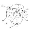
- FIG. 3schematically illustrates the functional processing of blocks in an MLC Flash memory device 100 according to an embodiment of the present invention having one type of MLC. It will be understood that FIG. 3 is a schematic illustration, and that blocks are not physically moved between or among pools, but rather various data structures, e.g., look-up tables, pointers, etc., which may be used to identify spare blocks of various types, blocks in use, and bad blocks, etc., may be modified as if to move or exchange an association of various blocks from spare block to block in use, or from block in use to bad block, etc.
- various data structurese.g., look-up tables, pointers, etc.
- Flash memory device 100may include an SLC flash memory array 110 and an MLC flash memory array 120 .
- the SLC flash memory array 110comprises an SLC used memory pool 130 and a number of spare blocks allocated as SLC spare blocks pool 140 .
- SLC spare blocks pool 140may initially be determined as a minimum number of spare blocks required for smooth functioning of the SLC memory array, such that only the minimum requisite spare blocks required for the SLC flash memory array 110 to function according to the SLC flash memory array 110 and flash memory device 100 specifications are initially provided.
- the MLC flash memory array 120also comprises an MLC used block pool 160 and an MLC spare block pool 150 . The remaining spare blocks, e.g., those spare blocks not assigned to the SLC spare block pool may be allocated to the MLC spare block pool 150 .
- the SLC flash memory array 110may require 10 usable SLC blocks and one spare SLC block at any arbitrary moment for smooth operation.
- a total of 11 SLC blocksmay therefore be allocated to the SLC flash memory array 110 at system initialization, ten blocks of which are for general use in the SLC used memory pool 130 , and one block of which is allocated to the SLC spare blocks pool 140 .
- the remaining blocksare allocated to the MLC spare block pool 150 .
- the memory controller 30may scan and test the flash memory arrays to identify bad blocks 170 .
- Various methodsare known for testing for bad blocks, which are not described herein for purposes of brevity. If a bad block 170 is discovered in the MLC flash memory array 120 , the MLC bad block may be exchanged with a spare block from the MLC spare block pool 150 . If a bad block is discovered in the SLC flash memory array 110 , the bad block may be exchanged with a spare block from the SLC spare blocks pool 140 .
- the memory devicemay require a predetermined minimum number of spare SLC blocks to be available at any time. Therefore, according to embodiments of the invention, when, for example, due to usage of SLC spare blocks, the number of available spare SLC blocks falls below this minimum, spare blocks from the MLC spare pool may be transferred, or re-allocated for use as SLC spare blocks as required.
- dynamic and static wear leveling operationsmay be performed within the SLC flash memory array 110 and the MLC flash memory array 120 .
- Dynamic and static wear leveling operationsmay be performed, for example, in order to extend the useful life of the Flash memory device.
- Each flash memory blockis typically rated for a certain number of P/E cycles.
- MLC blocksmay be rated for 3,000 P/E cycles and SLC blocks may be rated for 50,000 P/E cycles.
- Dynamic and static wear levelingmay prevent or delay some blocks of memory from exceeding a predetermined P/E cycle threshold while other blocks have endured fewer P/E cycles by distributing Flash cell erasures and re-writes evenly across the Flash memory array.
- MLC blocks from the MLC flash memory array 120 that reach a predetermined maximum MLC bearable P/E cyclesmay be transferred to the SLC spare block pool 140 and called into use as SLC blocks as required.
- a maximum number of bearable P/E cycles for an MLC blockmay be approximately 3,000 P/E cycles; a maximum number of bearable P/E cycles for an SLC block may be approximately 50,000 P/E cycles.
- MLC blockstherefore, may be used as SLC blocks after exceeding the maximum P/E cycle rating for an MLC block but while still less than the maximum P/E cycle rating for SLC blocks.
- SLC blocks that reach the maximum P/E cycle count for an SLC blockmay be declared bad blocks.
- the end of the Flash memory device's lifemay be declared when the number of remaining MLC spare blocks is zero.
- no more writesmay be allowed, and the device may be declared Read-Only.
- FIG. 4schematically illustrates an embodiment of the invention having three populations of block types, e.g., MLCx3, MLCx2, and SLC.
- Flash memory device 200comprises an SLC flash memory array 210 , a MLCx2 memory array 220 , and a MLCx3 memory array 230 .
- the SLC flash memory array 210comprises an SLC used memory pool 240 and a small number of spare blocks initially allocated to a SLC spare block pool 250 .
- a minimum number of spare blocks required for the smooth operation of SLC flash memory array 210may be initially provided.
- MLCx2 memory array 220comprises an MLCx2 used block pool 270 and a small number of spare blocks initially allocated to an MLCx2 spare block pool 280 .
- a minimum number of spare blocks required for the smooth operation of MLCx2 memory array 220may be initially provided.
- the MLCx2 spare block pool 280may function as a common spare block pool for the MLCx2 and SLC blocks in use.
- the remaining spare blocksmay be allocated to MLCx3 spare block pool 260 .
- the MLCx3 spare block pool 260may be used as MLCx3 spare blocks, MLCx2 spare blocks, and/or SLC spare blocks
- the MLCx3may function as a common spare block pool for the MLCx3, MLCx2 and SLC blocks in use.
- memory controller 30may regularly scan and test the memory arrays to identify bad blocks, e.g., a bad SLC block is discovered, or a SLC memory block has exceeded the prescribed maximum number of bearable P/E cycles.
- bad SLC blocks in use in SLC used memory pool 240may be exchanged for good SLC blocks from SLC spare block pool 250 .
- Bad MLCx2 blocks in use in MLCx2 used block pool 270may be exchanged for good MLCx2 blocks from MLCx2 spare block pool 280 .
- Bad MLCx3 blocks in use in MLCx3 blocks 290may be exchanged for good MLCx3 blocks from MLCx2 spare block pool 260 .
- the number of SLC blocks allocated to the SLC spare block poolmay be small, and therefore, the pool may be depleted of spare blocks after operation of SLC blocks in the device. Accordingly, if SLC blocks are no longer available in the SLC spare block pool, or if the number of spare blocks in the SLC spare block pool falls below a minimum threshold, e.g., a minimum number required for smooth operation of the SLC memory, a spare block from the MLCx2 spare block pool may be reallocated for the SLC spare block pool.
- a minimum thresholde.g., a minimum number required for smooth operation of the SLC memory
- the number of MLCx2 blocks allocated to the MLCx2 spare block poolmay be small, and therefore, the pool may be depleted of spare blocks after operation of MLCx2 blocks in the device. Accordingly, if MLCx2 blocks are no longer available in the MLCx2 spare block pool, or if the number of spare blocks in the MLCx2 spare block pool falls below a minimum threshold, e.g., a minimum number required for smooth operation of the MLCx2 memory, a spare block from the MLCx3 spare block pool may be reallocated for the MLCx2 spare block pool.
- a minimum thresholde.g., a minimum number required for smooth operation of the MLCx2 memory
- dynamic and static wear leveling operationsmay be performed in any one or more of the SLC flash memory array 210 , the MLCx2 memory array 220 , and the MLCx3 memory array 230 in order to increase the lifetime of the flash memory.
- MLCx3 blocks in use from the MLCx3 memory array 230 that reach maximum bearable cycle count for MLCx3 memorymay be transferred to the MLCx2 spare block pool 280 .
- MLCx2 blocks in the MLCx2 memory array 220 that reach maximum bearable cycle count specified for MLCx2 memorymay be transferred to SLC spare block pool 250 .
- SLC blocks that reach the maximum bearable P/E cycle count for an SLC blockmay be declared bad blocks 300 .
- the end of the Flash memory device 200 lifemay be declared to occur when the number of MLCx3 spare blocks is less than a predefined minimum spare blocks required for the X3 flash memory device 200 to operate according to specification.
- each of the lower levels of cell blocksmay be allotted the minimum number of spare blocks, and upon a type of spare block pool being depleted of spare blocks, additional spare blocks may be allocated from the spare block pool of a higher-order MLC block pool.
- the blockmay be reallocated as a spare block of type MLCx(j ⁇ 1). It will be understood that in an SLC block may be considered analogous to MLCx1.
- FIG. 5is a flowchart of a method for allocating and using spare pools of MLC and SLC blocks in Flash memory device 100 according to an embodiment of the present invention.
- a controllermay allocate a first portion of spare blocks as an SLC spare block pool (e.g., SLC spare blocks pool 140 of FIG. 3 ).
- the controllermay, in some embodiments, allocate a minimum number of spare blocks needed for smooth operation of the SLC memory cells (e.g., SLC flash memory array 110 of FIG. 3 ) and/or the Flash memory device (e.g., Flash memory device 100 of FIG. 1 ).
- the controllermay allocate a second portion of spare blocks as an MLC spare block pool (e.g., MLC spare block pool 150 of FIG. 3 ).
- the controllermay, in some embodiments, allocate to the MLC spare block pool all spare blocks not assigned to the SLC spare block pool.
- the controllermay replace bad SLC blocks in the Flash memory with spare blocks from the SLC spare block pool.
- An SLC block or other type of Flash memory blockmay become a bad block, for example, if the block is programmed and erased a number of times exceeding the P/E cycle maximum for the SLC block. Flash memory blocks may also become bad blocks by erase failure, or other causes.
- the controllermay replace bad MLC blocks in the Flash memory with spare blocks from the MLC spare block pool.
- the controllermay determine if the number of blocks in the SLC spare block pool is less than a minimum SLC spare pool threshold (e.g., the minimum number of SLC blocks necessary for smooth function of the SLC memory cells and/or the Flash memory device). If the number of blocks in the SLC spare block pool is less than a minimum SLC spare pool threshold, a process or the controller may proceed to operation 450 . If the number of blocks in the SLC spare block pool is equal to or greater than a minimum SLC spare pool threshold, a process or the controller may proceed to operation 420 .
- a minimum SLC spare pool thresholde.g., the minimum number of SLC blocks necessary for smooth function of the SLC memory cells and/or the Flash memory device.
- the controllermay re-allocate spare blocks from the MLC spare block pool to the SLC spare block pool.
- the controllermay, in some embodiments, transfer or re-allocate MLC spare blocks whose P/E cycles have exceeded the maximum P/E cycle rating for an MLC block but not the maximum P/E cycle rating for an SLC block. Any MLC block, or other type of block, that has not exceeded the maximum P/E cycle rating for SLC blocks may be re-allocated to the SLC spare block pool.
- the controllermay determine if the number of blocks in the MLC spare block pool is less than a minimum MLC spare pool threshold. If the number of blocks in the MLC spare block pool is less than a minimum MLC spare pool threshold, a process or controller may proceed to operation 470 . If the number of blocks in the MLC spare block pool is greater than or equal to a minimum MLC spare pool threshold, a process or controller may proceed to operation 420 .
- the controllermay declare an end of life of the Flash memory array.
- Embodiments of the inventionmay demonstrate one or move advantages, including, without requirement or limitation, ensuring optimal usage of all blocks throughout the life of the Flash memory device, increased spare block resources for the buffer and cache processes within the Flash device, longer Flash memory device lifespan, and/or reducing environmental waste from expired flash memory devices.
Landscapes
- Engineering & Computer Science (AREA)
- Theoretical Computer Science (AREA)
- Physics & Mathematics (AREA)
- General Engineering & Computer Science (AREA)
- General Physics & Mathematics (AREA)
- Techniques For Improving Reliability Of Storages (AREA)
Abstract
Description
Claims (16)
Priority Applications (1)
| Application Number | Priority Date | Filing Date | Title |
|---|---|---|---|
| US13/096,736US9021177B2 (en) | 2010-04-29 | 2011-04-28 | System and method for allocating and using spare blocks in a flash memory |
Applications Claiming Priority (2)
| Application Number | Priority Date | Filing Date | Title |
|---|---|---|---|
| US32936610P | 2010-04-29 | 2010-04-29 | |
| US13/096,736US9021177B2 (en) | 2010-04-29 | 2011-04-28 | System and method for allocating and using spare blocks in a flash memory |
Publications (2)
| Publication Number | Publication Date |
|---|---|
| US20110271043A1 US20110271043A1 (en) | 2011-11-03 |
| US9021177B2true US9021177B2 (en) | 2015-04-28 |
Family
ID=44859221
Family Applications (1)
| Application Number | Title | Priority Date | Filing Date |
|---|---|---|---|
| US13/096,736Active2032-04-22US9021177B2 (en) | 2010-04-29 | 2011-04-28 | System and method for allocating and using spare blocks in a flash memory |
Country Status (1)
| Country | Link |
|---|---|
| US (1) | US9021177B2 (en) |
Cited By (10)
| Publication number | Priority date | Publication date | Assignee | Title |
|---|---|---|---|---|
| US20160004615A1 (en)* | 2013-06-03 | 2016-01-07 | Hitachi, Ltd. | Storage apparatus and storage apparatus control method |
| US20170062069A1 (en)* | 2015-09-01 | 2017-03-02 | Sandisk Technologies Inc. | Dynamic management of programming states to improve endurance |
| US20170285953A1 (en)* | 2016-03-31 | 2017-10-05 | Silicon Motion, Inc. | Data Storage Device and Data Maintenance Method thereof |
| US20180260163A1 (en)* | 2017-03-07 | 2018-09-13 | Hefei Core Storage Electronic Limited | Data programming method, memory storage device and memory control circuit unit |
| US10101141B2 (en) | 2016-12-07 | 2018-10-16 | Mitutoyo Corporation | Trigger counter for measurement device with count values stored in flash memory |
| US20200081657A1 (en)* | 2018-09-07 | 2020-03-12 | Silicon Motion, Inc. | Data storage device and control method for non-volatile memory |
| US20200081621A1 (en)* | 2018-09-07 | 2020-03-12 | Silicon Motion, Inc. | Data storage device and control method for non-volatile memory |
| KR20200092252A (en)* | 2019-01-24 | 2020-08-03 | 웨스턴 디지털 테크놀로지스, 인코포레이티드 | Balancing the block wearing leveling for optimum ssd endurance |
| US11036411B2 (en) | 2019-06-24 | 2021-06-15 | Western Digital Technologies, Inc. | Yield improvement through block budget optimization by using a transient pool of multi-level blocks |
| US11036414B2 (en) | 2018-09-07 | 2021-06-15 | Silicon Motion, Inc. | Data storage device and control method for non-volatile memory with high-efficiency garbage collection |
Families Citing this family (100)
| Publication number | Priority date | Publication date | Assignee | Title |
|---|---|---|---|---|
| US8650352B2 (en) | 2007-09-20 | 2014-02-11 | Densbits Technologies Ltd. | Systems and methods for determining logical values of coupled flash memory cells |
| US8365040B2 (en) | 2007-09-20 | 2013-01-29 | Densbits Technologies Ltd. | Systems and methods for handling immediate data errors in flash memory |
| US8694715B2 (en) | 2007-10-22 | 2014-04-08 | Densbits Technologies Ltd. | Methods for adaptively programming flash memory devices and flash memory systems incorporating same |
| US8443242B2 (en) | 2007-10-25 | 2013-05-14 | Densbits Technologies Ltd. | Systems and methods for multiple coding rates in flash devices |
| US8335977B2 (en) | 2007-12-05 | 2012-12-18 | Densbits Technologies Ltd. | Flash memory apparatus and methods using a plurality of decoding stages including optional use of concatenated BCH codes and/or designation of “first below” cells |
| US8321625B2 (en) | 2007-12-05 | 2012-11-27 | Densbits Technologies Ltd. | Flash memory device with physical cell value deterioration accommodation and methods useful in conjunction therewith |
| WO2009072105A2 (en) | 2007-12-05 | 2009-06-11 | Densbits Technologies Ltd. | A low power chien-search based bch/rs decoding system for flash memory, mobile communications devices and other applications |
| US8276051B2 (en) | 2007-12-12 | 2012-09-25 | Densbits Technologies Ltd. | Chien-search system employing a clock-gating scheme to save power for error correction decoder and other applications |
| US8359516B2 (en) | 2007-12-12 | 2013-01-22 | Densbits Technologies Ltd. | Systems and methods for error correction and decoding on multi-level physical media |
| US8327246B2 (en) | 2007-12-18 | 2012-12-04 | Densbits Technologies Ltd. | Apparatus for coding at a plurality of rates in multi-level flash memory systems, and methods useful in conjunction therewith |
| WO2009118720A2 (en) | 2008-03-25 | 2009-10-01 | Densbits Technologies Ltd. | Apparatus and methods for hardware-efficient unbiased rounding |
| US8332725B2 (en) | 2008-08-20 | 2012-12-11 | Densbits Technologies Ltd. | Reprogramming non volatile memory portions |
| US8891298B2 (en) | 2011-07-19 | 2014-11-18 | Greenthread, Llc | Lifetime mixed level non-volatile memory system |
| US8819385B2 (en) | 2009-04-06 | 2014-08-26 | Densbits Technologies Ltd. | Device and method for managing a flash memory |
| US8458574B2 (en) | 2009-04-06 | 2013-06-04 | Densbits Technologies Ltd. | Compact chien-search based decoding apparatus and method |
| US8566510B2 (en) | 2009-05-12 | 2013-10-22 | Densbits Technologies Ltd. | Systems and method for flash memory management |
| US8305812B2 (en) | 2009-08-26 | 2012-11-06 | Densbits Technologies Ltd. | Flash memory module and method for programming a page of flash memory cells |
| US8995197B1 (en) | 2009-08-26 | 2015-03-31 | Densbits Technologies Ltd. | System and methods for dynamic erase and program control for flash memory device memories |
| US8868821B2 (en) | 2009-08-26 | 2014-10-21 | Densbits Technologies Ltd. | Systems and methods for pre-equalization and code design for a flash memory |
| US9330767B1 (en) | 2009-08-26 | 2016-05-03 | Avago Technologies General Ip (Singapore) Pte. Ltd. | Flash memory module and method for programming a page of flash memory cells |
| US8730729B2 (en) | 2009-10-15 | 2014-05-20 | Densbits Technologies Ltd. | Systems and methods for averaging error rates in non-volatile devices and storage systems |
| US8724387B2 (en) | 2009-10-22 | 2014-05-13 | Densbits Technologies Ltd. | Method, system, and computer readable medium for reading and programming flash memory cells using multiple bias voltages |
| US8626988B2 (en) | 2009-11-19 | 2014-01-07 | Densbits Technologies Ltd. | System and method for uncoded bit error rate equalization via interleaving |
| US9037777B2 (en) | 2009-12-22 | 2015-05-19 | Densbits Technologies Ltd. | Device, system, and method for reducing program/read disturb in flash arrays |
| US8607124B2 (en) | 2009-12-24 | 2013-12-10 | Densbits Technologies Ltd. | System and method for setting a flash memory cell read threshold |
| US8341502B2 (en) | 2010-02-28 | 2012-12-25 | Densbits Technologies Ltd. | System and method for multi-dimensional decoding |
| US8527840B2 (en) | 2010-04-06 | 2013-09-03 | Densbits Technologies Ltd. | System and method for restoring damaged data programmed on a flash device |
| US8516274B2 (en) | 2010-04-06 | 2013-08-20 | Densbits Technologies Ltd. | Method, system and medium for analog encryption in a flash memory |
| US8745317B2 (en) | 2010-04-07 | 2014-06-03 | Densbits Technologies Ltd. | System and method for storing information in a multi-level cell memory |
| US9021177B2 (en) | 2010-04-29 | 2015-04-28 | Densbits Technologies Ltd. | System and method for allocating and using spare blocks in a flash memory |
| US8539311B2 (en) | 2010-07-01 | 2013-09-17 | Densbits Technologies Ltd. | System and method for data recovery in multi-level cell memories |
| US8468431B2 (en) | 2010-07-01 | 2013-06-18 | Densbits Technologies Ltd. | System and method for multi-dimensional encoding and decoding |
| US20120008414A1 (en) | 2010-07-06 | 2012-01-12 | Michael Katz | Systems and methods for storing, retrieving, and adjusting read thresholds in flash memory storage system |
| US8964464B2 (en) | 2010-08-24 | 2015-02-24 | Densbits Technologies Ltd. | System and method for accelerated sampling |
| US8508995B2 (en) | 2010-09-15 | 2013-08-13 | Densbits Technologies Ltd. | System and method for adjusting read voltage thresholds in memories |
| US9063878B2 (en) | 2010-11-03 | 2015-06-23 | Densbits Technologies Ltd. | Method, system and computer readable medium for copy back |
| US8850100B2 (en) | 2010-12-07 | 2014-09-30 | Densbits Technologies Ltd. | Interleaving codeword portions between multiple planes and/or dies of a flash memory device |
| US10079068B2 (en) | 2011-02-23 | 2018-09-18 | Avago Technologies General Ip (Singapore) Pte. Ltd. | Devices and method for wear estimation based memory management |
| US8693258B2 (en) | 2011-03-17 | 2014-04-08 | Densbits Technologies Ltd. | Obtaining soft information using a hard interface |
| US8990665B1 (en) | 2011-04-06 | 2015-03-24 | Densbits Technologies Ltd. | System, method and computer program product for joint search of a read threshold and soft decoding |
| US9501392B1 (en) | 2011-05-12 | 2016-11-22 | Avago Technologies General Ip (Singapore) Pte. Ltd. | Management of a non-volatile memory module |
| US9110785B1 (en) | 2011-05-12 | 2015-08-18 | Densbits Technologies Ltd. | Ordered merge of data sectors that belong to memory space portions |
| US9396106B2 (en) | 2011-05-12 | 2016-07-19 | Avago Technologies General Ip (Singapore) Pte. Ltd. | Advanced management of a non-volatile memory |
| US9195592B1 (en) | 2011-05-12 | 2015-11-24 | Densbits Technologies Ltd. | Advanced management of a non-volatile memory |
| US8996790B1 (en) | 2011-05-12 | 2015-03-31 | Densbits Technologies Ltd. | System and method for flash memory management |
| US9372792B1 (en) | 2011-05-12 | 2016-06-21 | Avago Technologies General Ip (Singapore) Pte. Ltd. | Advanced management of a non-volatile memory |
| US8886911B2 (en)* | 2011-05-31 | 2014-11-11 | Micron Technology, Inc. | Dynamic memory cache size adjustment in a memory device |
| US8667211B2 (en) | 2011-06-01 | 2014-03-04 | Densbits Technologies Ltd. | System and method for managing a non-volatile memory |
| KR101756228B1 (en)* | 2011-07-19 | 2017-07-11 | 삼성전자 주식회사 | Memory apparatus |
| US8588003B1 (en) | 2011-08-01 | 2013-11-19 | Densbits Technologies Ltd. | System, method and computer program product for programming and for recovering from a power failure |
| US8553468B2 (en) | 2011-09-21 | 2013-10-08 | Densbits Technologies Ltd. | System and method for managing erase operations in a non-volatile memory |
| US9176862B2 (en)* | 2011-12-29 | 2015-11-03 | Sandisk Technologies Inc. | SLC-MLC wear balancing |
| US8996788B2 (en) | 2012-02-09 | 2015-03-31 | Densbits Technologies Ltd. | Configurable flash interface |
| US8947941B2 (en) | 2012-02-09 | 2015-02-03 | Densbits Technologies Ltd. | State responsive operations relating to flash memory cells |
| US8996793B1 (en) | 2012-04-24 | 2015-03-31 | Densbits Technologies Ltd. | System, method and computer readable medium for generating soft information |
| US8838937B1 (en) | 2012-05-23 | 2014-09-16 | Densbits Technologies Ltd. | Methods, systems and computer readable medium for writing and reading data |
| US8879325B1 (en) | 2012-05-30 | 2014-11-04 | Densbits Technologies Ltd. | System, method and computer program product for processing read threshold information and for reading a flash memory module |
| US8953398B2 (en) | 2012-06-19 | 2015-02-10 | Sandisk Technologies Inc. | Block level grading for reliability and yield improvement |
| US9921954B1 (en) | 2012-08-27 | 2018-03-20 | Avago Technologies General Ip (Singapore) Pte. Ltd. | Method and system for split flash memory management between host and storage controller |
| US9368225B1 (en) | 2012-11-21 | 2016-06-14 | Avago Technologies General Ip (Singapore) Pte. Ltd. | Determining read thresholds based upon read error direction statistics |
| US9069659B1 (en) | 2013-01-03 | 2015-06-30 | Densbits Technologies Ltd. | Read threshold determination using reference read threshold |
| US8954655B2 (en)* | 2013-01-14 | 2015-02-10 | Western Digital Technologies, Inc. | Systems and methods of configuring a mode of operation in a solid-state memory |
| KR20140142035A (en)* | 2013-06-03 | 2014-12-11 | 삼성전자주식회사 | Memory controller and method of operation of the memory controller |
| US9136876B1 (en) | 2013-06-13 | 2015-09-15 | Densbits Technologies Ltd. | Size limited multi-dimensional decoding |
| US9965199B2 (en)* | 2013-08-22 | 2018-05-08 | Sandisk Technologies Llc | Smart dynamic wear balancing between memory pools |
| US9413491B1 (en) | 2013-10-08 | 2016-08-09 | Avago Technologies General Ip (Singapore) Pte. Ltd. | System and method for multiple dimension decoding and encoding a message |
| US9348694B1 (en) | 2013-10-09 | 2016-05-24 | Avago Technologies General Ip (Singapore) Pte. Ltd. | Detecting and managing bad columns |
| US9397706B1 (en) | 2013-10-09 | 2016-07-19 | Avago Technologies General Ip (Singapore) Pte. Ltd. | System and method for irregular multiple dimension decoding and encoding |
| US9786388B1 (en) | 2013-10-09 | 2017-10-10 | Avago Technologies General Ip (Singapore) Pte. Ltd. | Detecting and managing bad columns |
| US9536612B1 (en) | 2014-01-23 | 2017-01-03 | Avago Technologies General Ip (Singapore) Pte. Ltd | Digital signaling processing for three dimensional flash memory arrays |
| US10120792B1 (en) | 2014-01-29 | 2018-11-06 | Avago Technologies General Ip (Singapore) Pte. Ltd. | Programming an embedded flash storage device |
| US9542262B1 (en) | 2014-05-29 | 2017-01-10 | Avago Technologies General Ip (Singapore) Pte. Ltd. | Error correction |
| US9892033B1 (en) | 2014-06-24 | 2018-02-13 | Avago Technologies General Ip (Singapore) Pte. Ltd. | Management of memory units |
| US9972393B1 (en) | 2014-07-03 | 2018-05-15 | Avago Technologies General Ip (Singapore) Pte. Ltd. | Accelerating programming of a flash memory module |
| US9584159B1 (en) | 2014-07-03 | 2017-02-28 | Avago Technologies General Ip (Singapore) Pte. Ltd. | Interleaved encoding |
| US9449702B1 (en) | 2014-07-08 | 2016-09-20 | Avago Technologies General Ip (Singapore) Pte. Ltd. | Power management |
| US10114562B2 (en)* | 2014-09-16 | 2018-10-30 | Sandisk Technologies Llc | Adaptive block allocation in nonvolatile memory |
| US9524211B1 (en) | 2014-11-18 | 2016-12-20 | Avago Technologies General Ip (Singapore) Pte. Ltd. | Codeword management |
| KR102295208B1 (en) | 2014-12-19 | 2021-09-01 | 삼성전자주식회사 | Storage device dynamically allocating program area and program method thererof |
| US10305515B1 (en) | 2015-02-02 | 2019-05-28 | Avago Technologies International Sales Pte. Limited | System and method for encoding using multiple linear feedback shift registers |
| TWI544490B (en)* | 2015-02-05 | 2016-08-01 | 慧榮科技股份有限公司 | Data storage device and data maintenance method thereof |
| US10628255B1 (en) | 2015-06-11 | 2020-04-21 | Avago Technologies International Sales Pte. Limited | Multi-dimensional decoding |
| US9851921B1 (en) | 2015-07-05 | 2017-12-26 | Avago Technologies General Ip (Singapore) Pte. Ltd. | Flash memory chip processing |
| US9983963B2 (en)* | 2015-11-09 | 2018-05-29 | Alibaba Group Holding Limited | System and method for exploiting hard disk drive capacity reserve and extending operating life thereof |
| US9954558B1 (en) | 2016-03-03 | 2018-04-24 | Avago Technologies General Ip (Singapore) Pte. Ltd. | Fast decoding of data stored in a flash memory |
| US10359933B2 (en) | 2016-09-19 | 2019-07-23 | Micron Technology, Inc. | Memory devices and electronic systems having a hybrid cache including static and dynamic caches with single and multiple bits per cell, and related methods |
| TWI640867B (en)* | 2017-05-02 | 2018-11-11 | 慧榮科技股份有限公司 | Data storage device and operating method therefor |
| US10838644B2 (en)* | 2017-12-06 | 2020-11-17 | Western Digital Technologies, Inc. | Data storage arrangement partitionable memory and method to accomplish partition |
| US11169747B2 (en) | 2018-10-30 | 2021-11-09 | Micron Technology, Inc. | Relocating data to low latency memory |
| US10877671B2 (en)* | 2018-12-03 | 2020-12-29 | Vast Data Ltd. | Techniques for prolonging lifespan of storage drives |
| KR102748625B1 (en)* | 2018-12-06 | 2024-12-31 | 에스케이하이닉스 주식회사 | Memory system and operating method thereof |
| US10956049B2 (en)* | 2019-06-12 | 2021-03-23 | International Business Machines Corporation | Wear-aware block mode conversion in non-volatile memory |
| US11182089B2 (en)* | 2019-07-01 | 2021-11-23 | International Business Machines.Corporation | Adapting memory block pool sizes using hybrid controllers |
| US11150825B2 (en)* | 2019-12-05 | 2021-10-19 | Microsoft Technology Licensing, Llc | Adaptive spare block usage in solid state drives |
| US11610641B2 (en)* | 2020-07-09 | 2023-03-21 | SK Hynix Inc. | Wafer-yields and write-QoS in flash-based solid state drives |
| WO2022011683A1 (en)* | 2020-07-17 | 2022-01-20 | Micron Technology, Inc. | Storage of video data and file system metadata |
| TWI788161B (en)* | 2021-12-27 | 2022-12-21 | 技嘉科技股份有限公司 | Control method for dynamically adjusting the ratio of single-level cells and three-level cells |
| US12009038B2 (en)* | 2022-04-20 | 2024-06-11 | Micron Technology, Inc. | Memory device wear leveling |
| US12430037B2 (en)* | 2023-02-10 | 2025-09-30 | SanDisk Technologies, Inc. | Illusory free data storage space in data storage devices |
| US12367138B1 (en)* | 2024-01-10 | 2025-07-22 | Sandisk Technologies Inc. | Method to extend the lifespan of a data storage device by repurposing blocks from burst pool |
Citations (215)
| Publication number | Priority date | Publication date | Assignee | Title |
|---|---|---|---|---|
| US4463375A (en) | 1982-09-07 | 1984-07-31 | The Board Of Trustees Of The Leland Standford Junior University | Multiple-measurement noise-reducing system |
| US4584686A (en) | 1983-12-22 | 1986-04-22 | Optical Storage International | Reed-Solomon error correction apparatus |
| US4589084A (en) | 1983-05-16 | 1986-05-13 | Rca Corporation | Apparatus for symmetrically truncating two's complement binary signals as for use with interleaved quadrature signals |
| US4866716A (en) | 1987-05-15 | 1989-09-12 | Digital Equipment Corporation | Real-time BCH error correction code decoding mechanism |
| US5077737A (en) | 1989-08-18 | 1991-12-31 | Micron Technology, Inc. | Method and apparatus for storing digital data in off-specification dynamic random access memory devices |
| US5297153A (en) | 1989-08-24 | 1994-03-22 | U.S. Philips Corporation | Method and apparatus for decoding code words protected wordwise by a non-binary BCH code from one or more symbol errors |
| US5657332A (en) | 1992-05-20 | 1997-08-12 | Sandisk Corporation | Soft errors handling in EEPROM devices |
| US5729490A (en) | 1995-07-31 | 1998-03-17 | Sgs-Thomson Microelectronics S.R.L. | Parallel-dichotomic serial sensing method for sensing multiple-level non-volatile memory cells, and sensing circuit for actuating such method |
| US5793774A (en) | 1994-11-04 | 1998-08-11 | Fujitsu Limited | Flash memory controlling system |
| US5926409A (en) | 1997-09-05 | 1999-07-20 | Information Storage Devices, Inc. | Method and apparatus for an adaptive ramp amplitude controller in nonvolatile memory application |
| US5956268A (en) | 1997-02-12 | 1999-09-21 | Hyundai Electronics America | Nonvolatile memory structure |
| US5982659A (en) | 1996-12-23 | 1999-11-09 | Lsi Logic Corporation | Memory cell capable of storing more than two logic states by using different via resistances |
| US6038634A (en) | 1998-02-02 | 2000-03-14 | International Business Machines Corporation | Intra-unit block addressing system for memory |
| US6094465A (en) | 1997-03-21 | 2000-07-25 | Qualcomm Incorporated | Method and apparatus for performing decoding of CRC outer concatenated codes |
| US6119245A (en) | 1997-08-06 | 2000-09-12 | Oki Electric Industry Co., Ltd. | Semiconductor storage device and method of controlling it |
| US6182261B1 (en) | 1998-11-05 | 2001-01-30 | Qualcomm Incorporated | Efficient iterative decoding |
| US6192497B1 (en) | 1998-08-27 | 2001-02-20 | Adaptec, Inc. | Parallel Chien search circuit |
| US6195287B1 (en) | 1999-02-03 | 2001-02-27 | Sharp Kabushiki Kaisha | Data programming method for a nonvolatile semiconductor storage |
| US6199188B1 (en) | 1997-10-07 | 2001-03-06 | Quantum Corporation | System for finding roots of degree three and degree four error locator polynomials over GF(2M) |
| US6209114B1 (en) | 1998-05-29 | 2001-03-27 | Texas Instruments Incorporated | Efficient hardware implementation of chien search polynomial reduction in reed-solomon decoding |
| US6259627B1 (en) | 2000-01-27 | 2001-07-10 | Multi Level Memory Technology | Read and write operations using constant row line voltage and variable column line load |
| US6279133B1 (en) | 1997-12-31 | 2001-08-21 | Kawasaki Steel Corporation | Method and apparatus for significantly improving the reliability of multilevel memory architecture |
| US6278633B1 (en) | 1999-11-05 | 2001-08-21 | Multi Level Memory Technology | High bandwidth flash memory that selects programming parameters according to measurements of previous programming operations |
| US6301151B1 (en) | 2000-08-09 | 2001-10-09 | Information Storage Devices, Inc. | Adaptive programming method and apparatus for flash memory analog storage |
| US6370061B1 (en) | 2001-06-19 | 2002-04-09 | Advanced Micro Devices, Inc. | Ceiling test mode to characterize the threshold voltage distribution of over programmed memory cells |
| US6374383B1 (en) | 1999-06-07 | 2002-04-16 | Maxtor Corporation | Determining error locations using error correction codes |
| US20020063774A1 (en) | 2000-11-29 | 2002-05-30 | Hillis William Daniel | Method and apparatus for maintaining eye contact in teleconferencing using reflected images |
| US20020085419A1 (en) | 2001-01-04 | 2002-07-04 | Seok-Cheon Kwon | Nonvolatile semiconductor memory device and data input/output control method thereof |
| US20020154769A1 (en) | 2000-12-07 | 2002-10-24 | Petersen Mette Vesterager | Method of generating pseudo-random numbers in an electronic device, and a method of encrypting and decrypting electronic data |
| US6504891B1 (en) | 1995-07-28 | 2003-01-07 | Micron Technology, Inc. | Timer circuit with programmable decode circuitry |
| US6532556B1 (en) | 2000-01-27 | 2003-03-11 | Multi Level Memory Technology | Data management for multi-bit-per-cell memories |
| US6532169B1 (en) | 2001-06-26 | 2003-03-11 | Cypress Semiconductor Corp. | SONOS latch and application |
| US20030065876A1 (en) | 2001-09-28 | 2003-04-03 | Menahem Lasser | Flash management system using only sequential Write |
| US6553533B2 (en) | 1998-02-05 | 2003-04-22 | International Business Machines Corporation | Method and apparatus for detecting and correcting errors and erasures in product ECC-coded data arrays for DVD and similar storage subsystems |
| US6560747B1 (en) | 1999-11-10 | 2003-05-06 | Maxtor Corporation | Error counting mechanism |
| US20030101404A1 (en) | 2001-11-01 | 2003-05-29 | Lijun Zhao | Inner coding of higher priority data within a digital message |
| US20030105620A1 (en) | 2001-01-29 | 2003-06-05 | Matt Bowen | System, method and article of manufacture for interface constructs in a programming language capable of programming hardware architetures |
| US20030192007A1 (en) | 2001-04-19 | 2003-10-09 | Miller David H. | Code-programmable field-programmable architecturally-systolic Reed-Solomon BCH error correction decoder integrated circuit and error correction decoding method |
| US6637002B1 (en) | 1998-10-21 | 2003-10-21 | Maxtor Corporation | Decoder for error correcting block codes |
| US6639865B2 (en) | 2000-10-25 | 2003-10-28 | Samsung Electronics Co., Ltd. | Memory device, method of accessing the memory device, and reed-solomon decoder including the memory device |
| US20040015771A1 (en) | 2002-07-16 | 2004-01-22 | Menahem Lasser | Error correction for non-volatile memory |
| US20040030971A1 (en) | 1999-06-28 | 2004-02-12 | Kabushiki Kaisha Toshiba | Flash memory |
| US6704902B1 (en) | 1998-09-07 | 2004-03-09 | Sony Corporation | Decoding system for error correction code |
| US6751766B2 (en) | 2002-05-20 | 2004-06-15 | Sandisk Corporation | Increasing the effectiveness of error correction codes and operating multi-level memory systems by using information about the quality of the stored data |
| US6772274B1 (en) | 2000-09-13 | 2004-08-03 | Lexar Media, Inc. | Flash memory system and method implementing LBA to PBA correlation within flash memory array |
| US20040153722A1 (en) | 2002-12-25 | 2004-08-05 | Heng-Kuan Lee | Error correction code circuit with reduced hardware complexity |
| US20040153817A1 (en) | 1996-10-24 | 2004-08-05 | Micron Technologies, Inc. | Apparatus and method for detecting over-programming condition in multistate memory device |
| US6781910B2 (en) | 2002-05-17 | 2004-08-24 | Hewlett-Packard Development Company, L.P. | Small area magnetic memory devices |
| US6792569B2 (en) | 2001-04-24 | 2004-09-14 | International Business Machines Corporation | Root solver and associated method for solving finite field polynomial equations |
| US20040181735A1 (en) | 2003-03-04 | 2004-09-16 | Weizhuang (Wayne) Xin | Decoding a received BCH encoded signal |
| US20050013165A1 (en) | 2003-06-17 | 2005-01-20 | Amir Ban | Flash memories with adaptive reference voltages |
| US20050018482A1 (en) | 2002-09-06 | 2005-01-27 | Raul-Adrian Cemea | Techniques for reducing effects of coupling between storage elements of adjacent rows of memory cells |
| US6873543B2 (en) | 2003-05-30 | 2005-03-29 | Hewlett-Packard Development Company, L.P. | Memory device |
| US20050083735A1 (en) | 2003-10-20 | 2005-04-21 | Jian Chen | Behavior based programming of non-volatile memory |
| US6891768B2 (en) | 2002-11-13 | 2005-05-10 | Hewlett-Packard Development Company, L.P. | Power-saving reading of magnetic memory devices |
| US20050117401A1 (en) | 2002-01-18 | 2005-06-02 | Jian Chen | Techniques of recovering data from memory cells affected by field coupling with adjacent memory cells |
| US20050120265A1 (en) | 2003-12-02 | 2005-06-02 | Pline Steven L. | Data storage system with error correction code and replaceable defective memory |
| US20050128811A1 (en) | 2002-05-23 | 2005-06-16 | Renesas Technology Corp. | Nonvolatile semiconductor memory device capable of uniformly inputting/outputting data |
| US20050138533A1 (en) | 2003-09-29 | 2005-06-23 | Canon Kabushiki Kaisha | Encoding/decoding device using a reed-solomon encoder/decoder |
| US20050144213A1 (en) | 2003-12-29 | 2005-06-30 | Xilinx, Inc. | Mathematical circuit with dynamic rounding |
| US20050144368A1 (en) | 2003-12-30 | 2005-06-30 | Samsung Electronics Co., Ltd. | Address mapping method and mapping information managing method for flash memory, and flash memory using the same |
| US6915477B2 (en) | 2001-12-28 | 2005-07-05 | Lucent Technologies Inc. | Delay sensitive adaptive quality control loop for rate adaptation |
| US6914809B2 (en) | 2003-07-07 | 2005-07-05 | Hewlett-Packard Development Company, L.P. | Memory cell strings |
| US20050172179A1 (en) | 2004-01-29 | 2005-08-04 | Brandenberger Sarah M. | System and method for configuring a solid-state storage device with error correction coding |
| US20050169057A1 (en) | 2004-01-30 | 2005-08-04 | Noboru Shibata | Semiconductor memory device which stores plural data in a cell |
| US20050213393A1 (en) | 2004-03-14 | 2005-09-29 | M-Systems Flash Disk Pioneers, Ltd. | States encoding in multi-bit flash cells for optimizing error rate |
| US6952365B2 (en) | 2002-01-18 | 2005-10-04 | Sandisk Corporation | Reducing the effects of noise in non-volatile memories through multiple reads |
| US6961890B2 (en) | 2001-08-16 | 2005-11-01 | Hewlett-Packard Development Company, L.P. | Dynamic variable-length error correction code |
| US6990012B2 (en) | 2003-10-07 | 2006-01-24 | Hewlett-Packard Development Company, L.P. | Magnetic memory device |
| US6996004B1 (en) | 2003-11-04 | 2006-02-07 | Advanced Micro Devices, Inc. | Minimization of FG-FG coupling in flash memory |
| US6999854B2 (en) | 2004-05-28 | 2006-02-14 | International Business Machines Corporation | Medical infusion pump capable of learning bolus time patterns and providing bolus alerts |
| US7010739B1 (en) | 2002-04-11 | 2006-03-07 | Marvell International Ltd. | Error evaluator for inversionless Berlekamp-Massey algorithm in Reed-Solomon decoders |
| US7012835B2 (en) | 2003-10-03 | 2006-03-14 | Sandisk Corporation | Flash memory data correction and scrub techniques |
| US20060059409A1 (en) | 2004-09-10 | 2006-03-16 | Hanho Lee | Reed-solomon decoder systems for high speed communication and data storage applications |
| US20060059406A1 (en) | 2004-09-10 | 2006-03-16 | Stmicroelectronics S.R.L. | Memory with embedded error correction codes |
| US20060064537A1 (en) | 2004-09-21 | 2006-03-23 | Takashi Oshima | Memory card having a storage cell and method of controlling the same |
| US7038950B1 (en) | 2004-11-05 | 2006-05-02 | Spansion Llc | Multi bit program algorithm |
| US20060101193A1 (en) | 2004-11-08 | 2006-05-11 | M-Systems Flash Disk Pioneers, Ltd. | States encoding in multi-bit flash cells for optimizing error rate |
| US7068539B2 (en) | 2004-01-27 | 2006-06-27 | Sandisk Corporation | Charge packet metering for coarse/fine programming of non-volatile memory |
| US7079436B2 (en) | 2003-09-30 | 2006-07-18 | Hewlett-Packard Development Company, L.P. | Resistive cross point memory |
| US20060203587A1 (en) | 2005-03-11 | 2006-09-14 | Yan Li | Partition of non-volatile memory array to reduce bit line capacitance |
| US20060221692A1 (en) | 2005-04-05 | 2006-10-05 | Jian Chen | Compensating for coupling during read operations on non-volatile memory |
| US20060248434A1 (en) | 2005-04-28 | 2006-11-02 | Micron Technology, Inc. | Non-systematic coded error correction |
| US20060268608A1 (en) | 2003-04-22 | 2006-11-30 | Kabushiki Kaisha Toshiba | Data storage system |
| US7149950B2 (en) | 2003-09-12 | 2006-12-12 | Hewlett-Packard Development Company, L.P. | Assisted memory device for reading and writing single and multiple units of data |
| US20060294312A1 (en) | 2004-05-27 | 2006-12-28 | Silverbrook Research Pty Ltd | Generation sequences |
| US20070025157A1 (en) | 2005-08-01 | 2007-02-01 | Jun Wan | Method for programming non-volatile memory with self-adjusting maximum program loop |
| US7177977B2 (en) | 2004-03-19 | 2007-02-13 | Sandisk Corporation | Operating non-volatile memory without read disturb limitations |
| US7191379B2 (en) | 2003-09-10 | 2007-03-13 | Hewlett-Packard Development Company, L.P. | Magnetic memory with error correction coding |
| US20070063180A1 (en) | 2005-09-07 | 2007-03-22 | Elpida Memory, Inc. | Electrically rewritable non-volatile memory element and method of manufacturing the same |
| US7196946B2 (en) | 2005-04-05 | 2007-03-27 | Sandisk Corporation | Compensating for coupling in non-volatile storage |
| US7203874B2 (en) | 2003-05-08 | 2007-04-10 | Micron Technology, Inc. | Error detection, documentation, and correction in a flash memory device |
| US20070103992A1 (en) | 2005-11-10 | 2007-05-10 | Sony Corporation | Memory system |
| US20070104004A1 (en) | 1997-09-08 | 2007-05-10 | So Hock C | Multi-Bit-Per-Cell Flash EEprom Memory with Refresh |
| US20070109858A1 (en) | 2000-12-28 | 2007-05-17 | Conley Kevin M | Novel Method and Structure for Efficient Data Verification Operation for Non-Volatile Memories |
| US20070124652A1 (en) | 2005-11-15 | 2007-05-31 | Ramot At Tel Aviv University Ltd. | Method and device for multi phase error-correction |
| US20070143561A1 (en) | 2005-12-21 | 2007-06-21 | Gorobets Sergey A | Methods for adaptive file data handling in non-volatile memories with a directly mapped file storage system |
| US20070150694A1 (en) | 2003-10-01 | 2007-06-28 | Sandisk Corporation | Hybrid Mapping Implementation Within a Non-Volatile Memory System |
| US20070168625A1 (en) | 2006-01-18 | 2007-07-19 | Cornwell Michael J | Interleaving policies for flash memory |
| US20070171714A1 (en) | 2006-01-20 | 2007-07-26 | Marvell International Ltd. | Flash memory with coding and signal processing |
| US20070171730A1 (en) | 2006-01-20 | 2007-07-26 | Marvell International Ltd. | Method and system for error correction in flash memory |
| US20070180346A1 (en) | 2006-01-18 | 2007-08-02 | Sandisk Il Ltd. | Method Of Arranging Data In A Multi-Level Cell Memory Device |
| US20070226582A1 (en) | 2006-03-08 | 2007-09-27 | Marvell International Ltd. | Systems and methods for achieving higher coding rate using parity interleaving |
| US20070226592A1 (en) | 2006-03-20 | 2007-09-27 | Micron Technology, Inc. | Variable sector-count ECC |
| US20070228449A1 (en) | 2006-03-31 | 2007-10-04 | Tamae Takano | Nonvolatile semiconductor memory device |
| US7290203B2 (en) | 2004-10-29 | 2007-10-30 | International Business Machines Corporation | Dynamic memory architecture employing passive expiration of data |
| US20070253249A1 (en) | 2006-04-26 | 2007-11-01 | Sang-Gu Kang | Multi-bit nonvolatile memory device and related programming method |
| US7292365B2 (en) | 2003-01-15 | 2007-11-06 | Xerox Corporation | Methods and systems for determining distribution mean level without histogram measurement |
| US20070263439A1 (en) | 2006-05-15 | 2007-11-15 | Apple Inc. | Dynamic Cell Bit Resolution |
| US20070266291A1 (en) | 2006-05-15 | 2007-11-15 | Kabushiki Kaisha Toshiba | Semiconductor memory device |
| US20070271494A1 (en) | 2006-05-17 | 2007-11-22 | Sandisk Corporation | Error Correction Coding for Multiple-Sector Pages in Flash Memory Devices |
| US7301928B2 (en) | 2004-06-09 | 2007-11-27 | Hitachi Kokusai Electric Inc. | Wireless packet transfer apparatus and method |
| US20080010581A1 (en) | 2006-07-04 | 2008-01-10 | Ramot At Tel Aviv University Ltd. | Method of error correction in a multi-bit-per-cell flash memory |
| US20080028014A1 (en) | 2006-07-26 | 2008-01-31 | Hilt Jason W | N-BIT 2's COMPLEMENT SYMMETRIC ROUNDING METHOD AND LOGIC FOR IMPLEMENTING THE SAME |
| US20080055989A1 (en) | 2006-09-06 | 2008-03-06 | Kyoong-Han Lee | Memory system including flash memory and method of operating the same |
| US20080082897A1 (en) | 2006-09-28 | 2008-04-03 | Yigal Brandman | Soft-Input Soft-Output Decoder for Nonvolatile Memory |
| US20080092026A1 (en) | 2006-09-28 | 2008-04-17 | Yigal Brandman | Methods of Soft-Input Soft-Output Decoding for Nonvolatile Memory |
| US20080104309A1 (en) | 2006-10-30 | 2008-05-01 | Cheon Won-Moon | Flash memory device with multi-level cells and method of writing data therein |
| US20080112238A1 (en)* | 2006-10-25 | 2008-05-15 | Seon-Taek Kim | Hybrid flash memory device and method for assigning reserved blocks thereof |
| US20080116509A1 (en) | 2001-10-31 | 2008-05-22 | Eliyahou Harari | Multi-State Non-Volatile Integrated Circuit Memory Systems that Employ Dielectric Storage Elements |
| US20080127104A1 (en) | 2006-11-27 | 2008-05-29 | Yan Li | Apparatus with segemented bitscan for verification of programming |
| US20080126686A1 (en) | 2006-11-28 | 2008-05-29 | Anobit Technologies Ltd. | Memory power and performance management |
| US20080128790A1 (en) | 2006-11-30 | 2008-06-05 | Jin-Hyo Jung | Memory device |
| US20080130341A1 (en) | 2006-12-03 | 2008-06-05 | Anobit Technologies Ltd. | Adaptive programming of analog memory |
| US20080137413A1 (en) | 2006-12-06 | 2008-06-12 | Samsung Electronics Co., Ltd | Multi-level cell memory devices using trellis coded modulation and methods of storing data in and reading data from the memory devices |
| US20080148115A1 (en) | 2006-12-17 | 2008-06-19 | Anobit Technologies Ltd. | High-speed programming of memory devices |
| US20080158958A1 (en) | 2006-12-17 | 2008-07-03 | Anobit Technologies Ltd. | Memory device with reduced reading |
| US20080162079A1 (en) | 2006-10-05 | 2008-07-03 | International Business Machines Corp. | End of life prediction of flash memory |
| US20080159059A1 (en) | 2007-01-03 | 2008-07-03 | Freescale Semiconductor, Inc. | Progressive memory initialization with waitpoints |
| US20080168216A1 (en) | 2007-01-09 | 2008-07-10 | Lee Seung-Jae | Memory system, multi-bit flash memory device, and associated methods |
| US20080168320A1 (en) | 2007-01-05 | 2008-07-10 | California Institute Of Technology | Codes For Limited Magnitude Asymetric Errors In Flash Memories |
| US20080181001A1 (en) | 2007-01-24 | 2008-07-31 | Anobit Technologies | Memory device with negative thresholds |
| US20080198652A1 (en) | 2006-05-12 | 2008-08-21 | Anobit Technologies Ltd. | Memory Device Programming Using Combined Shaping And Linear Spreading |
| US20080198650A1 (en) | 2006-05-12 | 2008-08-21 | Anobit Technologies Ltd. | Distortion Estimation And Cancellation In Memory Devices |
| US20080209114A1 (en)* | 1999-08-04 | 2008-08-28 | Super Talent Electronics, Inc. | Reliability High Endurance Non-Volatile Memory Device with Zone-Based Non-Volatile Memory File System |
| US20080219050A1 (en) | 2007-01-24 | 2008-09-11 | Anobit Technologies Ltd. | Reduction of back pattern dependency effects in memory devices |
| US20080225599A1 (en) | 2007-03-15 | 2008-09-18 | Samsung Electronics Co., Ltd. | Flash memory device with reduced coupling effect among cells and method of driving the same |
| US7441067B2 (en) | 2004-11-15 | 2008-10-21 | Sandisk Corporation | Cyclic flash memory wear leveling |
| US20080263262A1 (en) | 2007-04-22 | 2008-10-23 | Anobit Technologies Ltd. | Command interface for memory devices |
| US20080282106A1 (en) | 2007-05-12 | 2008-11-13 | Anobit Technologies Ltd | Data storage with incremental redundancy |
| US20080285351A1 (en) | 2007-05-14 | 2008-11-20 | Mark Shlick | Measuring threshold voltage distribution in memory using an aggregate characteristic |
| US20080301532A1 (en) | 2006-09-25 | 2008-12-04 | Kabushiki Kaisha Toshiba | Non-volatile semiconductor memory device |
| US20090024905A1 (en) | 2006-05-12 | 2009-01-22 | Anobit Technologies Ltd. | Combined distortion estimation and error correction coding for memory devices |
| US20090043951A1 (en) | 2007-08-06 | 2009-02-12 | Anobit Technologies Ltd. | Programming schemes for multi-level analog memory cells |
| US20090072303A9 (en) | 2002-06-21 | 2009-03-19 | Micron Technology, Inc. | Nrom memory cell, memory array, related devices and methods |
| US20090091979A1 (en) | 2007-10-08 | 2009-04-09 | Anobit Technologies | Reliable data storage in analog memory cells in the presence of temperature variations |
| US20090106485A1 (en) | 2007-10-19 | 2009-04-23 | Anobit Technologies Ltd. | Reading analog memory cells using built-in multi-threshold commands |
| US20090103358A1 (en) | 2006-05-12 | 2009-04-23 | Anobit Technologies Ltd. | Reducing programming error in memory devices |
| US20090113275A1 (en) | 2007-10-29 | 2009-04-30 | Legend Silicon Corp. | Bch code with 256 information bytes and up to 8 bytes of parity check elements |
| US20090125671A1 (en) | 2006-12-06 | 2009-05-14 | David Flynn | Apparatus, system, and method for storage space recovery after reaching a read count limit |
| US20090144600A1 (en) | 2007-11-30 | 2009-06-04 | Anobit Technologies Ltd | Efficient re-read operations from memory devices |
| US20090150748A1 (en) | 2004-08-02 | 2009-06-11 | Koninklijke Philips Electronics N.V. | Data Storage and Replay Apparatus |
| US20090158126A1 (en) | 2007-12-12 | 2009-06-18 | Anobit Technologies Ltd | Efficient interference cancellation in analog memory cell arrays |
| US20090157964A1 (en) | 2007-12-16 | 2009-06-18 | Anobit Technologies Ltd. | Efficient data storage in multi-plane memory devices |
| US20090168524A1 (en) | 2007-12-27 | 2009-07-02 | Anobit Technologies Ltd. | Wear level estimation in analog memory cells |
| US7558109B2 (en) | 2006-11-03 | 2009-07-07 | Sandisk Corporation | Nonvolatile memory with variable read threshold |
| US20090187803A1 (en) | 2008-01-21 | 2009-07-23 | Anobit Technologies Ltd. | Decoding of error correction code using partial bit inversion |
| US20090199074A1 (en) | 2008-02-05 | 2009-08-06 | Anobit Technologies Ltd. | Parameter estimation based on error correction code parity check equations |
| US20090213653A1 (en) | 2008-02-21 | 2009-08-27 | Anobit Technologies Ltd | Programming of analog memory cells using a single programming pulse per state transition |
| US20090213654A1 (en) | 2008-02-24 | 2009-08-27 | Anobit Technologies Ltd | Programming analog memory cells for reduced variance after retention |
| US20090228761A1 (en) | 2008-03-07 | 2009-09-10 | Anobit Technologies Ltd | Efficient readout from analog memory cells using data compression |
| US20090240872A1 (en) | 2008-03-18 | 2009-09-24 | Anobit Technologies Ltd | Memory device with multiple-accuracy read commands |
| US20090300269A1 (en)* | 2008-05-28 | 2009-12-03 | Radke William H | Hybrid memory management |
| US20100005270A1 (en) | 2008-03-07 | 2010-01-07 | Via Technologies, Inc. | Storage unit management methods and systems |
| US20100058146A1 (en) | 2007-12-12 | 2010-03-04 | Hanan Weingarten | Chien-search system employing a clock-gating scheme to save power for error correction decoder and other applications |
| US20100064096A1 (en) | 2007-12-05 | 2010-03-11 | Hanan Weingarten | Systems and methods for temporarily retiring memory portions |
| US20100088557A1 (en) | 2007-10-25 | 2010-04-08 | Hanan Weingarten | Systems and methods for multiple coding rates in flash devices |
| US20100091535A1 (en) | 2007-03-12 | 2010-04-15 | Anobit Technologies Ltd | Adaptive estimation of memory cell read thresholds |
| US20100095186A1 (en) | 2008-08-20 | 2010-04-15 | Hanan Weingarten | Reprogramming non volatile memory portions |
| US20100115376A1 (en) | 2006-12-03 | 2010-05-06 | Anobit Technologies Ltd. | Automatic defect management in memory devices |
| US20100110787A1 (en) | 2006-10-30 | 2010-05-06 | Anobit Technologies Ltd. | Memory cell readout using successive approximation |
| US20100122113A1 (en) | 2007-09-20 | 2010-05-13 | Hanan Weingarten | Systems and methods for handling immediate data errors in flash memory |
| US20100124088A1 (en) | 2008-11-16 | 2010-05-20 | Anobit Technologies Ltd | Storage at m bits/cell density in n bits/cell analog memory cell devices, m>n |
| US20100131831A1 (en) | 2007-12-05 | 2010-05-27 | Hanan Weingarten | low power chien-search based bch/rs decoding system for flash memory, mobile communications devices and other applications |
| US20100131826A1 (en) | 2006-08-27 | 2010-05-27 | Anobit Technologies Ltd. | Estimation of non-linear distortion in memory devices |
| US20100131580A1 (en) | 2008-03-25 | 2010-05-27 | Densbits Technologies Ltd. | Apparatus and methods for hardware-efficient unbiased rounding |
| US20100131806A1 (en) | 2007-12-18 | 2010-05-27 | Hanan Weingarten | Apparatus for coding at a plurality of rates in multi-level flash memory systems, and methods useful in conjunction therewith |
| US20100131827A1 (en) | 2007-05-12 | 2010-05-27 | Anobit Technologies Ltd | Memory device with internal signap processing unit |
| US20100146192A1 (en) | 2007-10-22 | 2010-06-10 | Hanan Weingarten | Methods for adaptively programming flash memory devices and flash memory systems incorporating same |
| US20100149881A1 (en) | 2008-12-11 | 2010-06-17 | Shih-Chung Lee | Adaptive erase and soft programming for memory |
| US20100172179A1 (en)* | 2009-01-05 | 2010-07-08 | Sergey Anatolievich Gorobets | Spare Block Management of Non-Volatile Memories |
| US20100199149A1 (en) | 2007-12-05 | 2010-08-05 | Hanan Weingarten | Flash memory apparatus and methods using a plurality of decoding stages including optional use of concatenated bch codes and/or designation of "first below" cells |
| US20100211724A1 (en) | 2007-09-20 | 2010-08-19 | Hanan Weingarten | Systems and methods for determining logical values of coupled flash memory cells |
| US20100211856A1 (en) | 2007-12-12 | 2010-08-19 | Hanan Weingarten | Systems and methods for error correction and decoding on multi-level physical media |
| US20100211833A1 (en) | 2007-10-22 | 2010-08-19 | Hanan Weingarten | Systems and methods for averaging error rates in non-volatile devices and storage systems |
| US20100241793A1 (en)* | 2008-04-25 | 2010-09-23 | Hitachi, Ltd. | Storage system and method for controlling storage system |
| US7805663B2 (en) | 2006-09-28 | 2010-09-28 | Sandisk Corporation | Methods of adapting operation of nonvolatile memory |
| US7805664B1 (en) | 2006-10-05 | 2010-09-28 | Marvell International Ltd | Likelihood metric generation for trellis-based detection and/or decoding |
| US7804718B2 (en) | 2007-03-07 | 2010-09-28 | Mosaid Technologies Incorporated | Partial block erase architecture for flash memory |
| US20100251066A1 (en) | 2006-08-31 | 2010-09-30 | Micron Technology, Inc. | Data handling |
| US20100257309A1 (en) | 2009-04-06 | 2010-10-07 | Boris Barsky | Device and method for managing a flash memory |
| US20100253555A1 (en) | 2009-04-06 | 2010-10-07 | Hanan Weingarten | Encoding method and system, decoding method and system |
| US20100293321A1 (en) | 2009-05-12 | 2010-11-18 | Hanan Weingarten | Systems and method for flash memory management |
| US20110055461A1 (en) | 2009-08-26 | 2011-03-03 | Steiner Avi | Systems and methods for pre-equalization and code design for a flash memory |
| US20110051521A1 (en) | 2009-08-26 | 2011-03-03 | Shmuel Levy | Flash memory module and method for programming a page of flash memory cells |
| US20110096612A1 (en) | 2009-10-22 | 2011-04-28 | Steiner Avi | Method, system, and computer readable medium for reading and programming flash memory cells |
| US20110119562A1 (en) | 2009-11-19 | 2011-05-19 | Steiner Avi | System and method for uncoded bit error rate equalization via interleaving |
| US7961797B1 (en) | 2006-10-10 | 2011-06-14 | Marvell International Ltd. | Nonlinear viterbi complexity reduction |
| US20110153919A1 (en) | 2009-12-22 | 2011-06-23 | Erez Sabbag | Device, system, and method for reducing program/read disturb in flash arrays |
| US20110161775A1 (en) | 2009-12-24 | 2011-06-30 | Hanan Weingarten | System and method for setting a flash memory cell read threshold |
| US20110214039A1 (en) | 2010-02-28 | 2011-09-01 | Steiner Avi | System and method for multi-dimensional decoding |
| US20110246852A1 (en) | 2010-04-06 | 2011-10-06 | Erez Sabbag | System and method for restoring damaged data programmed on a flash device |
| US20110246792A1 (en) | 2010-04-06 | 2011-10-06 | Hanan Weingarten | Method, system and medium for analog encryption in a flash memory |
| US20110252187A1 (en) | 2010-04-07 | 2011-10-13 | Avigdor Segal | System and method for operating a non-volatile memory including a portion operating as a single-level cell memory and a portion operating as a multi-level cell memory |
| US20110252188A1 (en) | 2010-04-07 | 2011-10-13 | Hanan Weingarten | System and method for storing information in a multi-level cell memory |
| US20110271043A1 (en) | 2010-04-29 | 2011-11-03 | Avigdor Segal | System and method for allocating and using spare blocks in a flash memory |
| US20120005560A1 (en) | 2010-07-01 | 2012-01-05 | Steiner Avi | System and method for multi-dimensional encoding and decoding |
| US20120005558A1 (en) | 2010-07-01 | 2012-01-05 | Steiner Avi | System and method for data recovery in multi-level cell memories |
| US20120008401A1 (en) | 2010-07-06 | 2012-01-12 | Michael Katz | Systems and methods for storing, retrieving, and adjusting read thresholds in flash memory storage system |
| US8122328B2 (en) | 2007-03-30 | 2012-02-21 | Samsung Electronics Co., Ltd. | Bose-Chaudhuri-Hocquenghem error correction method and circuit for checking error using error correction encoder |
| US20120051144A1 (en) | 2010-08-24 | 2012-03-01 | Hanan Weingarten | System and method for accelerated sampling |
| US20120063227A1 (en) | 2010-09-15 | 2012-03-15 | Hanan Weingarten | System and method for adjusting read voltage thresholds in memories |
| US20120066441A1 (en) | 2009-10-15 | 2012-03-15 | Densbits Technologies Ltd. | Systems and methods for averaging error rates in non-volatile devices and storage systems |
| US20120110250A1 (en) | 2010-11-03 | 2012-05-03 | Densbits Technologies Ltd. | Meethod, system and computer readable medium for copy back |
| US20120246391A1 (en)* | 2011-01-27 | 2012-09-27 | Anobit Technologies | Block management schemes in hybrid slc/mlc memory |
- 2011
- 2011-04-28USUS13/096,736patent/US9021177B2/enactiveActive
Patent Citations (233)
| Publication number | Priority date | Publication date | Assignee | Title |
|---|---|---|---|---|
| US4463375A (en) | 1982-09-07 | 1984-07-31 | The Board Of Trustees Of The Leland Standford Junior University | Multiple-measurement noise-reducing system |
| US4589084A (en) | 1983-05-16 | 1986-05-13 | Rca Corporation | Apparatus for symmetrically truncating two's complement binary signals as for use with interleaved quadrature signals |
| US4584686A (en) | 1983-12-22 | 1986-04-22 | Optical Storage International | Reed-Solomon error correction apparatus |
| US4866716A (en) | 1987-05-15 | 1989-09-12 | Digital Equipment Corporation | Real-time BCH error correction code decoding mechanism |
| US5077737A (en) | 1989-08-18 | 1991-12-31 | Micron Technology, Inc. | Method and apparatus for storing digital data in off-specification dynamic random access memory devices |
| US5297153A (en) | 1989-08-24 | 1994-03-22 | U.S. Philips Corporation | Method and apparatus for decoding code words protected wordwise by a non-binary BCH code from one or more symbol errors |
| US5657332A (en) | 1992-05-20 | 1997-08-12 | Sandisk Corporation | Soft errors handling in EEPROM devices |
| US5793774A (en) | 1994-11-04 | 1998-08-11 | Fujitsu Limited | Flash memory controlling system |
| US6504891B1 (en) | 1995-07-28 | 2003-01-07 | Micron Technology, Inc. | Timer circuit with programmable decode circuitry |
| US5729490A (en) | 1995-07-31 | 1998-03-17 | Sgs-Thomson Microelectronics S.R.L. | Parallel-dichotomic serial sensing method for sensing multiple-level non-volatile memory cells, and sensing circuit for actuating such method |
| US20040153817A1 (en) | 1996-10-24 | 2004-08-05 | Micron Technologies, Inc. | Apparatus and method for detecting over-programming condition in multistate memory device |
| US5982659A (en) | 1996-12-23 | 1999-11-09 | Lsi Logic Corporation | Memory cell capable of storing more than two logic states by using different via resistances |
| US5956268A (en) | 1997-02-12 | 1999-09-21 | Hyundai Electronics America | Nonvolatile memory structure |
| US6094465A (en) | 1997-03-21 | 2000-07-25 | Qualcomm Incorporated | Method and apparatus for performing decoding of CRC outer concatenated codes |
| US6119245A (en) | 1997-08-06 | 2000-09-12 | Oki Electric Industry Co., Ltd. | Semiconductor storage device and method of controlling it |
| US5926409A (en) | 1997-09-05 | 1999-07-20 | Information Storage Devices, Inc. | Method and apparatus for an adaptive ramp amplitude controller in nonvolatile memory application |
| US20070104004A1 (en) | 1997-09-08 | 2007-05-10 | So Hock C | Multi-Bit-Per-Cell Flash EEprom Memory with Refresh |
| US6199188B1 (en) | 1997-10-07 | 2001-03-06 | Quantum Corporation | System for finding roots of degree three and degree four error locator polynomials over GF(2M) |
| US6279133B1 (en) | 1997-12-31 | 2001-08-21 | Kawasaki Steel Corporation | Method and apparatus for significantly improving the reliability of multilevel memory architecture |
| US6038634A (en) | 1998-02-02 | 2000-03-14 | International Business Machines Corporation | Intra-unit block addressing system for memory |
| US6553533B2 (en) | 1998-02-05 | 2003-04-22 | International Business Machines Corporation | Method and apparatus for detecting and correcting errors and erasures in product ECC-coded data arrays for DVD and similar storage subsystems |
| US6209114B1 (en) | 1998-05-29 | 2001-03-27 | Texas Instruments Incorporated | Efficient hardware implementation of chien search polynomial reduction in reed-solomon decoding |
| US6192497B1 (en) | 1998-08-27 | 2001-02-20 | Adaptec, Inc. | Parallel Chien search circuit |
| US6704902B1 (en) | 1998-09-07 | 2004-03-09 | Sony Corporation | Decoding system for error correction code |
| US6637002B1 (en) | 1998-10-21 | 2003-10-21 | Maxtor Corporation | Decoder for error correcting block codes |
| US6182261B1 (en) | 1998-11-05 | 2001-01-30 | Qualcomm Incorporated | Efficient iterative decoding |
| US6195287B1 (en) | 1999-02-03 | 2001-02-27 | Sharp Kabushiki Kaisha | Data programming method for a nonvolatile semiconductor storage |
| US6374383B1 (en) | 1999-06-07 | 2002-04-16 | Maxtor Corporation | Determining error locations using error correction codes |
| US20070223277A1 (en) | 1999-06-28 | 2007-09-27 | Kabushiki Kaisha Toshiba | Flash memory |
| US20040030971A1 (en) | 1999-06-28 | 2004-02-12 | Kabushiki Kaisha Toshiba | Flash memory |
| US20080209114A1 (en)* | 1999-08-04 | 2008-08-28 | Super Talent Electronics, Inc. | Reliability High Endurance Non-Volatile Memory Device with Zone-Based Non-Volatile Memory File System |
| US6278633B1 (en) | 1999-11-05 | 2001-08-21 | Multi Level Memory Technology | High bandwidth flash memory that selects programming parameters according to measurements of previous programming operations |
| US6560747B1 (en) | 1999-11-10 | 2003-05-06 | Maxtor Corporation | Error counting mechanism |
| US6259627B1 (en) | 2000-01-27 | 2001-07-10 | Multi Level Memory Technology | Read and write operations using constant row line voltage and variable column line load |
| US6532556B1 (en) | 2000-01-27 | 2003-03-11 | Multi Level Memory Technology | Data management for multi-bit-per-cell memories |
| US6301151B1 (en) | 2000-08-09 | 2001-10-09 | Information Storage Devices, Inc. | Adaptive programming method and apparatus for flash memory analog storage |
| US6772274B1 (en) | 2000-09-13 | 2004-08-03 | Lexar Media, Inc. | Flash memory system and method implementing LBA to PBA correlation within flash memory array |
| US6639865B2 (en) | 2000-10-25 | 2003-10-28 | Samsung Electronics Co., Ltd. | Memory device, method of accessing the memory device, and reed-solomon decoder including the memory device |
| US20020063774A1 (en) | 2000-11-29 | 2002-05-30 | Hillis William Daniel | Method and apparatus for maintaining eye contact in teleconferencing using reflected images |
| US20020154769A1 (en) | 2000-12-07 | 2002-10-24 | Petersen Mette Vesterager | Method of generating pseudo-random numbers in an electronic device, and a method of encrypting and decrypting electronic data |
| US20070109858A1 (en) | 2000-12-28 | 2007-05-17 | Conley Kevin M | Novel Method and Structure for Efficient Data Verification Operation for Non-Volatile Memories |
| US20020085419A1 (en) | 2001-01-04 | 2002-07-04 | Seok-Cheon Kwon | Nonvolatile semiconductor memory device and data input/output control method thereof |
| US20030105620A1 (en) | 2001-01-29 | 2003-06-05 | Matt Bowen | System, method and article of manufacture for interface constructs in a programming language capable of programming hardware architetures |
| US20030192007A1 (en) | 2001-04-19 | 2003-10-09 | Miller David H. | Code-programmable field-programmable architecturally-systolic Reed-Solomon BCH error correction decoder integrated circuit and error correction decoding method |
| US6792569B2 (en) | 2001-04-24 | 2004-09-14 | International Business Machines Corporation | Root solver and associated method for solving finite field polynomial equations |
| US6370061B1 (en) | 2001-06-19 | 2002-04-09 | Advanced Micro Devices, Inc. | Ceiling test mode to characterize the threshold voltage distribution of over programmed memory cells |
| US6674665B1 (en) | 2001-06-26 | 2004-01-06 | Cypress Semiconductor Corp. | SONOS latch and application |
| US6532169B1 (en) | 2001-06-26 | 2003-03-11 | Cypress Semiconductor Corp. | SONOS latch and application |
| US6961890B2 (en) | 2001-08-16 | 2005-11-01 | Hewlett-Packard Development Company, L.P. | Dynamic variable-length error correction code |
| US20030065876A1 (en) | 2001-09-28 | 2003-04-03 | Menahem Lasser | Flash management system using only sequential Write |
| US20080116509A1 (en) | 2001-10-31 | 2008-05-22 | Eliyahou Harari | Multi-State Non-Volatile Integrated Circuit Memory Systems that Employ Dielectric Storage Elements |
| US20030101404A1 (en) | 2001-11-01 | 2003-05-29 | Lijun Zhao | Inner coding of higher priority data within a digital message |
| US6915477B2 (en) | 2001-12-28 | 2005-07-05 | Lucent Technologies Inc. | Delay sensitive adaptive quality control loop for rate adaptation |
| US6952365B2 (en) | 2002-01-18 | 2005-10-04 | Sandisk Corporation | Reducing the effects of noise in non-volatile memories through multiple reads |
| US20050117401A1 (en) | 2002-01-18 | 2005-06-02 | Jian Chen | Techniques of recovering data from memory cells affected by field coupling with adjacent memory cells |
| US7010739B1 (en) | 2002-04-11 | 2006-03-07 | Marvell International Ltd. | Error evaluator for inversionless Berlekamp-Massey algorithm in Reed-Solomon decoders |
| US6781910B2 (en) | 2002-05-17 | 2004-08-24 | Hewlett-Packard Development Company, L.P. | Small area magnetic memory devices |
| US6751766B2 (en) | 2002-05-20 | 2004-06-15 | Sandisk Corporation | Increasing the effectiveness of error correction codes and operating multi-level memory systems by using information about the quality of the stored data |
| US20050128811A1 (en) | 2002-05-23 | 2005-06-16 | Renesas Technology Corp. | Nonvolatile semiconductor memory device capable of uniformly inputting/outputting data |
| US20090072303A9 (en) | 2002-06-21 | 2009-03-19 | Micron Technology, Inc. | Nrom memory cell, memory array, related devices and methods |
| US20040015771A1 (en) | 2002-07-16 | 2004-01-22 | Menahem Lasser | Error correction for non-volatile memory |
| US20050018482A1 (en) | 2002-09-06 | 2005-01-27 | Raul-Adrian Cemea | Techniques for reducing effects of coupling between storage elements of adjacent rows of memory cells |
| US6891768B2 (en) | 2002-11-13 | 2005-05-10 | Hewlett-Packard Development Company, L.P. | Power-saving reading of magnetic memory devices |
| US20040153722A1 (en) | 2002-12-25 | 2004-08-05 | Heng-Kuan Lee | Error correction code circuit with reduced hardware complexity |
| US7292365B2 (en) | 2003-01-15 | 2007-11-06 | Xerox Corporation | Methods and systems for determining distribution mean level without histogram measurement |
| US20040181735A1 (en) | 2003-03-04 | 2004-09-16 | Weizhuang (Wayne) Xin | Decoding a received BCH encoded signal |
| US20060268608A1 (en) | 2003-04-22 | 2006-11-30 | Kabushiki Kaisha Toshiba | Data storage system |
| US7203874B2 (en) | 2003-05-08 | 2007-04-10 | Micron Technology, Inc. | Error detection, documentation, and correction in a flash memory device |
| US6873543B2 (en) | 2003-05-30 | 2005-03-29 | Hewlett-Packard Development Company, L.P. | Memory device |
| US20050013165A1 (en) | 2003-06-17 | 2005-01-20 | Amir Ban | Flash memories with adaptive reference voltages |
| US6914809B2 (en) | 2003-07-07 | 2005-07-05 | Hewlett-Packard Development Company, L.P. | Memory cell strings |
| US7191379B2 (en) | 2003-09-10 | 2007-03-13 | Hewlett-Packard Development Company, L.P. | Magnetic memory with error correction coding |
| US7149950B2 (en) | 2003-09-12 | 2006-12-12 | Hewlett-Packard Development Company, L.P. | Assisted memory device for reading and writing single and multiple units of data |
| US20050138533A1 (en) | 2003-09-29 | 2005-06-23 | Canon Kabushiki Kaisha | Encoding/decoding device using a reed-solomon encoder/decoder |
| US7079436B2 (en) | 2003-09-30 | 2006-07-18 | Hewlett-Packard Development Company, L.P. | Resistive cross point memory |
| US20070150694A1 (en) | 2003-10-01 | 2007-06-28 | Sandisk Corporation | Hybrid Mapping Implementation Within a Non-Volatile Memory System |
| US7012835B2 (en) | 2003-10-03 | 2006-03-14 | Sandisk Corporation | Flash memory data correction and scrub techniques |
| US6990012B2 (en) | 2003-10-07 | 2006-01-24 | Hewlett-Packard Development Company, L.P. | Magnetic memory device |
| US20050083735A1 (en) | 2003-10-20 | 2005-04-21 | Jian Chen | Behavior based programming of non-volatile memory |
| US6996004B1 (en) | 2003-11-04 | 2006-02-07 | Advanced Micro Devices, Inc. | Minimization of FG-FG coupling in flash memory |
| US20050120265A1 (en) | 2003-12-02 | 2005-06-02 | Pline Steven L. | Data storage system with error correction code and replaceable defective memory |
| US20050144213A1 (en) | 2003-12-29 | 2005-06-30 | Xilinx, Inc. | Mathematical circuit with dynamic rounding |
| US20050144368A1 (en) | 2003-12-30 | 2005-06-30 | Samsung Electronics Co., Ltd. | Address mapping method and mapping information managing method for flash memory, and flash memory using the same |
| US7068539B2 (en) | 2004-01-27 | 2006-06-27 | Sandisk Corporation | Charge packet metering for coarse/fine programming of non-volatile memory |
| US20050172179A1 (en) | 2004-01-29 | 2005-08-04 | Brandenberger Sarah M. | System and method for configuring a solid-state storage device with error correction coding |
| US20070253250A1 (en) | 2004-01-30 | 2007-11-01 | Noboru Shibata | Semiconductor memory device which stores plural data in a cell |
| US20050169057A1 (en) | 2004-01-30 | 2005-08-04 | Noboru Shibata | Semiconductor memory device which stores plural data in a cell |
| US20050213393A1 (en) | 2004-03-14 | 2005-09-29 | M-Systems Flash Disk Pioneers, Ltd. | States encoding in multi-bit flash cells for optimizing error rate |
| US7177977B2 (en) | 2004-03-19 | 2007-02-13 | Sandisk Corporation | Operating non-volatile memory without read disturb limitations |
| US20060294312A1 (en) | 2004-05-27 | 2006-12-28 | Silverbrook Research Pty Ltd | Generation sequences |
| US6999854B2 (en) | 2004-05-28 | 2006-02-14 | International Business Machines Corporation | Medical infusion pump capable of learning bolus time patterns and providing bolus alerts |
| US7301928B2 (en) | 2004-06-09 | 2007-11-27 | Hitachi Kokusai Electric Inc. | Wireless packet transfer apparatus and method |
| US20090150748A1 (en) | 2004-08-02 | 2009-06-11 | Koninklijke Philips Electronics N.V. | Data Storage and Replay Apparatus |
| US20060059406A1 (en) | 2004-09-10 | 2006-03-16 | Stmicroelectronics S.R.L. | Memory with embedded error correction codes |
| US20060059409A1 (en) | 2004-09-10 | 2006-03-16 | Hanho Lee | Reed-solomon decoder systems for high speed communication and data storage applications |
| US20060064537A1 (en) | 2004-09-21 | 2006-03-23 | Takashi Oshima | Memory card having a storage cell and method of controlling the same |
| US8020073B2 (en) | 2004-10-29 | 2011-09-13 | International Business Machines Corporation | Dynamic memory architecture employing passive expiration of data |
| US7290203B2 (en) | 2004-10-29 | 2007-10-30 | International Business Machines Corporation | Dynamic memory architecture employing passive expiration of data |
| US7038950B1 (en) | 2004-11-05 | 2006-05-02 | Spansion Llc | Multi bit program algorithm |
| US20060101193A1 (en) | 2004-11-08 | 2006-05-11 | M-Systems Flash Disk Pioneers, Ltd. | States encoding in multi-bit flash cells for optimizing error rate |
| US7441067B2 (en) | 2004-11-15 | 2008-10-21 | Sandisk Corporation | Cyclic flash memory wear leveling |
| US20060203587A1 (en) | 2005-03-11 | 2006-09-14 | Yan Li | Partition of non-volatile memory array to reduce bit line capacitance |
| US7196946B2 (en) | 2005-04-05 | 2007-03-27 | Sandisk Corporation | Compensating for coupling in non-volatile storage |
| US20060221692A1 (en) | 2005-04-05 | 2006-10-05 | Jian Chen | Compensating for coupling during read operations on non-volatile memory |
| US20060248434A1 (en) | 2005-04-28 | 2006-11-02 | Micron Technology, Inc. | Non-systematic coded error correction |
| US20070025157A1 (en) | 2005-08-01 | 2007-02-01 | Jun Wan | Method for programming non-volatile memory with self-adjusting maximum program loop |
| US20070063180A1 (en) | 2005-09-07 | 2007-03-22 | Elpida Memory, Inc. | Electrically rewritable non-volatile memory element and method of manufacturing the same |
| US20070103992A1 (en) | 2005-11-10 | 2007-05-10 | Sony Corporation | Memory system |
| US20070124652A1 (en) | 2005-11-15 | 2007-05-31 | Ramot At Tel Aviv University Ltd. | Method and device for multi phase error-correction |
| US7844877B2 (en) | 2005-11-15 | 2010-11-30 | Ramot At Tel Aviv University Ltd. | Method and device for multi phase error-correction |
| US20070143561A1 (en) | 2005-12-21 | 2007-06-21 | Gorobets Sergey A | Methods for adaptive file data handling in non-volatile memories with a directly mapped file storage system |
| US20070168625A1 (en) | 2006-01-18 | 2007-07-19 | Cornwell Michael J | Interleaving policies for flash memory |
| US20070180346A1 (en) | 2006-01-18 | 2007-08-02 | Sandisk Il Ltd. | Method Of Arranging Data In A Multi-Level Cell Memory Device |
| US20070171714A1 (en) | 2006-01-20 | 2007-07-26 | Marvell International Ltd. | Flash memory with coding and signal processing |
| US20070171730A1 (en) | 2006-01-20 | 2007-07-26 | Marvell International Ltd. | Method and system for error correction in flash memory |
| US20070226582A1 (en) | 2006-03-08 | 2007-09-27 | Marvell International Ltd. | Systems and methods for achieving higher coding rate using parity interleaving |
| US20070226592A1 (en) | 2006-03-20 | 2007-09-27 | Micron Technology, Inc. | Variable sector-count ECC |
| US20070228449A1 (en) | 2006-03-31 | 2007-10-04 | Tamae Takano | Nonvolatile semiconductor memory device |
| US20070253249A1 (en) | 2006-04-26 | 2007-11-01 | Sang-Gu Kang | Multi-bit nonvolatile memory device and related programming method |
| US7466575B2 (en) | 2006-05-12 | 2008-12-16 | Anobit Technologies Ltd. | Memory device programming using combined shaping and linear spreading |
| US20090103358A1 (en) | 2006-05-12 | 2009-04-23 | Anobit Technologies Ltd. | Reducing programming error in memory devices |
| US20090024905A1 (en) | 2006-05-12 | 2009-01-22 | Anobit Technologies Ltd. | Combined distortion estimation and error correction coding for memory devices |
| US7697326B2 (en) | 2006-05-12 | 2010-04-13 | Anobit Technologies Ltd. | Reducing programming error in memory devices |
| US20080198652A1 (en) | 2006-05-12 | 2008-08-21 | Anobit Technologies Ltd. | Memory Device Programming Using Combined Shaping And Linear Spreading |
| US20080198650A1 (en) | 2006-05-12 | 2008-08-21 | Anobit Technologies Ltd. | Distortion Estimation And Cancellation In Memory Devices |
| US20070266291A1 (en) | 2006-05-15 | 2007-11-15 | Kabushiki Kaisha Toshiba | Semiconductor memory device |
| US20070263439A1 (en) | 2006-05-15 | 2007-11-15 | Apple Inc. | Dynamic Cell Bit Resolution |
| US20070271494A1 (en) | 2006-05-17 | 2007-11-22 | Sandisk Corporation | Error Correction Coding for Multiple-Sector Pages in Flash Memory Devices |
| US7533328B2 (en) | 2006-07-04 | 2009-05-12 | Sandisk Il, Ltd. | Method of error correction in a multi-bit-per-cell flash memory |
| US20080010581A1 (en) | 2006-07-04 | 2008-01-10 | Ramot At Tel Aviv University Ltd. | Method of error correction in a multi-bit-per-cell flash memory |
| US20080028014A1 (en) | 2006-07-26 | 2008-01-31 | Hilt Jason W | N-BIT 2's COMPLEMENT SYMMETRIC ROUNDING METHOD AND LOGIC FOR IMPLEMENTING THE SAME |
| US20100131826A1 (en) | 2006-08-27 | 2010-05-27 | Anobit Technologies Ltd. | Estimation of non-linear distortion in memory devices |
| US20100251066A1 (en) | 2006-08-31 | 2010-09-30 | Micron Technology, Inc. | Data handling |
| US20080055989A1 (en) | 2006-09-06 | 2008-03-06 | Kyoong-Han Lee | Memory system including flash memory and method of operating the same |
| US20080301532A1 (en) | 2006-09-25 | 2008-12-04 | Kabushiki Kaisha Toshiba | Non-volatile semiconductor memory device |
| US20080092026A1 (en) | 2006-09-28 | 2008-04-17 | Yigal Brandman | Methods of Soft-Input Soft-Output Decoding for Nonvolatile Memory |
| US20080082897A1 (en) | 2006-09-28 | 2008-04-03 | Yigal Brandman | Soft-Input Soft-Output Decoder for Nonvolatile Memory |
| US7805663B2 (en) | 2006-09-28 | 2010-09-28 | Sandisk Corporation | Methods of adapting operation of nonvolatile memory |
| US20080162079A1 (en) | 2006-10-05 | 2008-07-03 | International Business Machines Corp. | End of life prediction of flash memory |
| US7805664B1 (en) | 2006-10-05 | 2010-09-28 | Marvell International Ltd | Likelihood metric generation for trellis-based detection and/or decoding |
| US7961797B1 (en) | 2006-10-10 | 2011-06-14 | Marvell International Ltd. | Nonlinear viterbi complexity reduction |
| US20080112238A1 (en)* | 2006-10-25 | 2008-05-15 | Seon-Taek Kim | Hybrid flash memory device and method for assigning reserved blocks thereof |
| US20080104309A1 (en) | 2006-10-30 | 2008-05-01 | Cheon Won-Moon | Flash memory device with multi-level cells and method of writing data therein |
| US20100110787A1 (en) | 2006-10-30 | 2010-05-06 | Anobit Technologies Ltd. | Memory cell readout using successive approximation |
| US7558109B2 (en) | 2006-11-03 | 2009-07-07 | Sandisk Corporation | Nonvolatile memory with variable read threshold |
| US20080127104A1 (en) | 2006-11-27 | 2008-05-29 | Yan Li | Apparatus with segemented bitscan for verification of programming |
| US20080126686A1 (en) | 2006-11-28 | 2008-05-29 | Anobit Technologies Ltd. | Memory power and performance management |
| US20080128790A1 (en) | 2006-11-30 | 2008-06-05 | Jin-Hyo Jung | Memory device |
| US20080130341A1 (en) | 2006-12-03 | 2008-06-05 | Anobit Technologies Ltd. | Adaptive programming of analog memory |
| US20100115376A1 (en) | 2006-12-03 | 2010-05-06 | Anobit Technologies Ltd. | Automatic defect management in memory devices |
| US7706182B2 (en) | 2006-12-03 | 2010-04-27 | Anobit Technologies Ltd. | Adaptive programming of analog memory cells using statistical characteristics |
| US20080137413A1 (en) | 2006-12-06 | 2008-06-12 | Samsung Electronics Co., Ltd | Multi-level cell memory devices using trellis coded modulation and methods of storing data in and reading data from the memory devices |
| US20090125671A1 (en) | 2006-12-06 | 2009-05-14 | David Flynn | Apparatus, system, and method for storage space recovery after reaching a read count limit |
| US7593263B2 (en) | 2006-12-17 | 2009-09-22 | Anobit Technologies Ltd. | Memory device with reduced reading latency |
| US20080148115A1 (en) | 2006-12-17 | 2008-06-19 | Anobit Technologies Ltd. | High-speed programming of memory devices |
| US20080158958A1 (en) | 2006-12-17 | 2008-07-03 | Anobit Technologies Ltd. | Memory device with reduced reading |
| US20080159059A1 (en) | 2007-01-03 | 2008-07-03 | Freescale Semiconductor, Inc. | Progressive memory initialization with waitpoints |
| US20080168320A1 (en) | 2007-01-05 | 2008-07-10 | California Institute Of Technology | Codes For Limited Magnitude Asymetric Errors In Flash Memories |
| US20080168216A1 (en) | 2007-01-09 | 2008-07-10 | Lee Seung-Jae | Memory system, multi-bit flash memory device, and associated methods |
| US20080219050A1 (en) | 2007-01-24 | 2008-09-11 | Anobit Technologies Ltd. | Reduction of back pattern dependency effects in memory devices |
| US20080181001A1 (en) | 2007-01-24 | 2008-07-31 | Anobit Technologies | Memory device with negative thresholds |
| US7804718B2 (en) | 2007-03-07 | 2010-09-28 | Mosaid Technologies Incorporated | Partial block erase architecture for flash memory |
| US20100091535A1 (en) | 2007-03-12 | 2010-04-15 | Anobit Technologies Ltd | Adaptive estimation of memory cell read thresholds |
| US20080225599A1 (en) | 2007-03-15 | 2008-09-18 | Samsung Electronics Co., Ltd. | Flash memory device with reduced coupling effect among cells and method of driving the same |
| US8122328B2 (en) | 2007-03-30 | 2012-02-21 | Samsung Electronics Co., Ltd. | Bose-Chaudhuri-Hocquenghem error correction method and circuit for checking error using error correction encoder |
| US20080263262A1 (en) | 2007-04-22 | 2008-10-23 | Anobit Technologies Ltd. | Command interface for memory devices |
| US20100131827A1 (en) | 2007-05-12 | 2010-05-27 | Anobit Technologies Ltd | Memory device with internal signap processing unit |
| US20080282106A1 (en) | 2007-05-12 | 2008-11-13 | Anobit Technologies Ltd | Data storage with incremental redundancy |
| US20080285351A1 (en) | 2007-05-14 | 2008-11-20 | Mark Shlick | Measuring threshold voltage distribution in memory using an aggregate characteristic |
| US20090043951A1 (en) | 2007-08-06 | 2009-02-12 | Anobit Technologies Ltd. | Programming schemes for multi-level analog memory cells |
| US20100122113A1 (en) | 2007-09-20 | 2010-05-13 | Hanan Weingarten | Systems and methods for handling immediate data errors in flash memory |
| US20100211724A1 (en) | 2007-09-20 | 2010-08-19 | Hanan Weingarten | Systems and methods for determining logical values of coupled flash memory cells |
| US20090091979A1 (en) | 2007-10-08 | 2009-04-09 | Anobit Technologies | Reliable data storage in analog memory cells in the presence of temperature variations |
| US20090106485A1 (en) | 2007-10-19 | 2009-04-23 | Anobit Technologies Ltd. | Reading analog memory cells using built-in multi-threshold commands |
| US20100211833A1 (en) | 2007-10-22 | 2010-08-19 | Hanan Weingarten | Systems and methods for averaging error rates in non-volatile devices and storage systems |
| US20100146192A1 (en) | 2007-10-22 | 2010-06-10 | Hanan Weingarten | Methods for adaptively programming flash memory devices and flash memory systems incorporating same |
| US20100088557A1 (en) | 2007-10-25 | 2010-04-08 | Hanan Weingarten | Systems and methods for multiple coding rates in flash devices |
| US20090113275A1 (en) | 2007-10-29 | 2009-04-30 | Legend Silicon Corp. | Bch code with 256 information bytes and up to 8 bytes of parity check elements |
| US20090144600A1 (en) | 2007-11-30 | 2009-06-04 | Anobit Technologies Ltd | Efficient re-read operations from memory devices |
| US20100131831A1 (en) | 2007-12-05 | 2010-05-27 | Hanan Weingarten | low power chien-search based bch/rs decoding system for flash memory, mobile communications devices and other applications |
| US20100131809A1 (en) | 2007-12-05 | 2010-05-27 | Michael Katz | Apparatus and methods for generating row-specific reading thresholds in flash memory |
| US20100199149A1 (en) | 2007-12-05 | 2010-08-05 | Hanan Weingarten | Flash memory apparatus and methods using a plurality of decoding stages including optional use of concatenated bch codes and/or designation of "first below" cells |
| US20100064096A1 (en) | 2007-12-05 | 2010-03-11 | Hanan Weingarten | Systems and methods for temporarily retiring memory portions |
| US20100180073A1 (en) | 2007-12-05 | 2010-07-15 | Hanan Weingarten | Flash memory device with physical cell value deterioration accommodation and methods useful in conjunction therewith |
| US20100146191A1 (en) | 2007-12-05 | 2010-06-10 | Michael Katz | System and methods employing mock thresholds to generate actual reading thresholds in flash memory devices |
| US20100211856A1 (en) | 2007-12-12 | 2010-08-19 | Hanan Weingarten | Systems and methods for error correction and decoding on multi-level physical media |
| US20100058146A1 (en) | 2007-12-12 | 2010-03-04 | Hanan Weingarten | Chien-search system employing a clock-gating scheme to save power for error correction decoder and other applications |
| US20090158126A1 (en) | 2007-12-12 | 2009-06-18 | Anobit Technologies Ltd | Efficient interference cancellation in analog memory cell arrays |
| US20090157964A1 (en) | 2007-12-16 | 2009-06-18 | Anobit Technologies Ltd. | Efficient data storage in multi-plane memory devices |
| US20100131806A1 (en) | 2007-12-18 | 2010-05-27 | Hanan Weingarten | Apparatus for coding at a plurality of rates in multi-level flash memory systems, and methods useful in conjunction therewith |
| US20090168524A1 (en) | 2007-12-27 | 2009-07-02 | Anobit Technologies Ltd. | Wear level estimation in analog memory cells |
| US20090187803A1 (en) | 2008-01-21 | 2009-07-23 | Anobit Technologies Ltd. | Decoding of error correction code using partial bit inversion |
| US20090199074A1 (en) | 2008-02-05 | 2009-08-06 | Anobit Technologies Ltd. | Parameter estimation based on error correction code parity check equations |
| US20090213653A1 (en) | 2008-02-21 | 2009-08-27 | Anobit Technologies Ltd | Programming of analog memory cells using a single programming pulse per state transition |
| US20090213654A1 (en) | 2008-02-24 | 2009-08-27 | Anobit Technologies Ltd | Programming analog memory cells for reduced variance after retention |
| US20100005270A1 (en) | 2008-03-07 | 2010-01-07 | Via Technologies, Inc. | Storage unit management methods and systems |
| US20090228761A1 (en) | 2008-03-07 | 2009-09-10 | Anobit Technologies Ltd | Efficient readout from analog memory cells using data compression |
| US20090240872A1 (en) | 2008-03-18 | 2009-09-24 | Anobit Technologies Ltd | Memory device with multiple-accuracy read commands |
| US20100131580A1 (en) | 2008-03-25 | 2010-05-27 | Densbits Technologies Ltd. | Apparatus and methods for hardware-efficient unbiased rounding |
| US20100241793A1 (en)* | 2008-04-25 | 2010-09-23 | Hitachi, Ltd. | Storage system and method for controlling storage system |
| US20090300269A1 (en)* | 2008-05-28 | 2009-12-03 | Radke William H | Hybrid memory management |
| US20100095186A1 (en) | 2008-08-20 | 2010-04-15 | Hanan Weingarten | Reprogramming non volatile memory portions |
| US20100124088A1 (en) | 2008-11-16 | 2010-05-20 | Anobit Technologies Ltd | Storage at m bits/cell density in n bits/cell analog memory cell devices, m>n |
| US20100149881A1 (en) | 2008-12-11 | 2010-06-17 | Shih-Chung Lee | Adaptive erase and soft programming for memory |
| US20100172179A1 (en)* | 2009-01-05 | 2010-07-08 | Sergey Anatolievich Gorobets | Spare Block Management of Non-Volatile Memories |
| US20100257309A1 (en) | 2009-04-06 | 2010-10-07 | Boris Barsky | Device and method for managing a flash memory |
| US20100253555A1 (en) | 2009-04-06 | 2010-10-07 | Hanan Weingarten | Encoding method and system, decoding method and system |
| US20100293321A1 (en) | 2009-05-12 | 2010-11-18 | Hanan Weingarten | Systems and method for flash memory management |
| US20110051521A1 (en) | 2009-08-26 | 2011-03-03 | Shmuel Levy | Flash memory module and method for programming a page of flash memory cells |
| US20110055461A1 (en) | 2009-08-26 | 2011-03-03 | Steiner Avi | Systems and methods for pre-equalization and code design for a flash memory |
| US20120066441A1 (en) | 2009-10-15 | 2012-03-15 | Densbits Technologies Ltd. | Systems and methods for averaging error rates in non-volatile devices and storage systems |
| US20110096612A1 (en) | 2009-10-22 | 2011-04-28 | Steiner Avi | Method, system, and computer readable medium for reading and programming flash memory cells |
| US20110119562A1 (en) | 2009-11-19 | 2011-05-19 | Steiner Avi | System and method for uncoded bit error rate equalization via interleaving |
| US20110153919A1 (en) | 2009-12-22 | 2011-06-23 | Erez Sabbag | Device, system, and method for reducing program/read disturb in flash arrays |
| US20110161775A1 (en) | 2009-12-24 | 2011-06-30 | Hanan Weingarten | System and method for setting a flash memory cell read threshold |
| US20110214039A1 (en) | 2010-02-28 | 2011-09-01 | Steiner Avi | System and method for multi-dimensional decoding |
| US20110214029A1 (en) | 2010-02-28 | 2011-09-01 | Steiner Avi | System and method for multi-dimensional decoding |
| US20110246852A1 (en) | 2010-04-06 | 2011-10-06 | Erez Sabbag | System and method for restoring damaged data programmed on a flash device |
| US20110302428A1 (en) | 2010-04-06 | 2011-12-08 | Hanan Weingarten | Method, system and medium for analog encryption in a flash memory |
| US20110246792A1 (en) | 2010-04-06 | 2011-10-06 | Hanan Weingarten | Method, system and medium for analog encryption in a flash memory |
| US20110252187A1 (en) | 2010-04-07 | 2011-10-13 | Avigdor Segal | System and method for operating a non-volatile memory including a portion operating as a single-level cell memory and a portion operating as a multi-level cell memory |
| US20110252188A1 (en) | 2010-04-07 | 2011-10-13 | Hanan Weingarten | System and method for storing information in a multi-level cell memory |
| US20110271043A1 (en) | 2010-04-29 | 2011-11-03 | Avigdor Segal | System and method for allocating and using spare blocks in a flash memory |
| US20120005560A1 (en) | 2010-07-01 | 2012-01-05 | Steiner Avi | System and method for multi-dimensional encoding and decoding |
| US20120005554A1 (en) | 2010-07-01 | 2012-01-05 | Steiner Avi | System and method for multi-dimensional encoding and decoding |
| US20120005558A1 (en) | 2010-07-01 | 2012-01-05 | Steiner Avi | System and method for data recovery in multi-level cell memories |
| US20120001778A1 (en) | 2010-07-01 | 2012-01-05 | Steiner Avi | System and method for multi-dimensional encoding and decoding |
| US20120008401A1 (en) | 2010-07-06 | 2012-01-12 | Michael Katz | Systems and methods for storing, retrieving, and adjusting read thresholds in flash memory storage system |
| US20120008414A1 (en) | 2010-07-06 | 2012-01-12 | Michael Katz | Systems and methods for storing, retrieving, and adjusting read thresholds in flash memory storage system |
| US20120051144A1 (en) | 2010-08-24 | 2012-03-01 | Hanan Weingarten | System and method for accelerated sampling |
| US20120063227A1 (en) | 2010-09-15 | 2012-03-15 | Hanan Weingarten | System and method for adjusting read voltage thresholds in memories |
| US20120110250A1 (en) | 2010-11-03 | 2012-05-03 | Densbits Technologies Ltd. | Meethod, system and computer readable medium for copy back |
| US20120246391A1 (en)* | 2011-01-27 | 2012-09-27 | Anobit Technologies | Block management schemes in hybrid slc/mlc memory |
Non-Patent Citations (37)
| Title |
|---|
| Akash Kumar, Sergei Sawitzki, "High-Throughput and Low Power Architectures for Reed Solomon Decoder", (a.kumar at tue.nl, Eindhoven University of Technology and sergei.sawitzki at philips.com). |
| Berlekamp et al., "On the Solution of Algebraic Equations over Finite Fields", Inform. Cont. 10, Oct. 1967, pp. 553-564. |
| Boaz Eitan, Guy Cohen, Assaf Shappir, Eli Lusky, Amichai Givant, Meir Janai, Ilan Bloom, Yan Polansky, Oleg Dadashev, Avi Lavan, Ran Sahar, Eduardo Maayan, "4-bit per Cell NROM Reliability", Appears on the website of Saifun.com. |
| Chen, Formulas for the solutions of Quadratic Equations over GF (2), IEEE Trans. Inform. Theory, vol. IT-28, No. 5, Sep. 1982, pp. 792-794. |
| Daneshbeh, "Bit Serial Systolic Architectures for Multiplicative Inversion and Division over GF (2)", A thesis presented to the University of Waterloo, Ontario, Canada, 2005, pp. 1-118. |
| David Esseni, Bruno Ricco, "Trading-Off Programming Speed and Current Absorption in Flash Memories with the Ramped-Gate Programming Technique", leee Transactions on Electron Devices, vol. 47, No. 4, Apr. 2000. |
| Dempster, et al., "Maximum Likelihood from Incomplete Data via the EM Algorithm", Journal of the Royal Statistical Society. Series B (Methodological), vol. 39, No. 1 (1997), pp. 1-38. |
| G. Tao, A. Scarpa, J. Dijkstra, W. Stidl, F. Kuper, "Data retention prediction for modern floating gate non-volatile memories", Microelectronics Reliability 40 (2000), 1561-1566. |
| Giovanni Campardo, Rino Micheloni, David Novosel, "VLSI-Design of Non-Volatile Memories", Springer Berlin Heidelberg New York, 2005. |
| J.M. Portal, H. Aziza, D. Nee, "EEPROM Diagnosis Based on Threshold Voltage Embedded Measurement", Journal of Electronic Testing: Theory and Applications 21, 33-42, 2005. |
| J.M. Portal, H. Aziza, D. Nee, "EEPROM Memory: Threshold Voltage Built in Self Diagnosis", ITC International Test Conference, Paper 2.1. |
| JEDEC STANDARD, "Stress-Test-Driven Qualification of Integrated Circuits", JEDEC Solid State Technology Association. JEDEC Standard No. 47F pp. 1-26. |
| John G. Proakis, "Digital Communications", 3rd ed., New York: McGraw-Hill, 1995. |
| Michael Purser, "Introduction to Error Correcting Codes", Artech House Inc., 1995. |
| Mielke, et al., "Flash EEPROM Threshold Instabilities due to Charge Trapping During Program/Erase Cycling", IEEE Transactions on Device and Materials Reliability, vol. 4, No. 3, Sep. 2004, pp. 335-344. |
| Paulo Cappelletti, Clara Golla, Piero Olivo, Enrico Zanoni, "Flash Memories", Kluwer Academic Publishers, 1999. |
| Richard E. Blahut, "Algebraic Codes for Data Transmission", Cambridge University Press, 2003. |
| Ron M. Roth, "Introduction to Coding Theory", Cambridge University Press, 2006. |
| Search Report of PCT Patent Application WO 2009/072101 A3. |
| Search Report of PCT Patent Application WO 2009/072102 A3. |
| Search Report of PCT Patent Application WO 2009/072103 A3. |
| Search Report of PCT Patent Application WO 2009/072104 A3. |
| Search Report of PCT Patent Application WO 2009/072105 A3. |
| Search Report of PCT Patent Application WO 2009/074978 A3. |
| Search Report of PCT Patent Application WO 2009/074979 A3. |
| Search Report of PCT Patent Application WO 2009/078006 A3. |
| Search Report of PCT Patent Application WO 2009/095902 A3. |
| Search Report of PCT Patent Application WO 2009/118720 A3. |
| Search Report of PCT Patent Application WO 20091037697 A3. |
| Search Report of PCT Patent Application WO 20091053961 A3. |
| Search Report of PCT Patent Application WO 20091053962 A3. |
| Search Report of PCT Patent Application WO 20091053963 A3. |
| Search Report of PCT Patent Application WO 20091072100 A3. |
| T. Hirncno, N. Matsukawa, H. Hazama, K. Sakui, M. Oshikiri, K. Masuda, K. Kanda, Y. Itoh, J. Miyamoto, "A New Technique for Measuring Threshold Voltage Distribution in Flash EEPROM Devices", Proc. IEEE 1995 Int. Conference on Microelectronics Test Structures, vol. 8, Mar. 1995. |
| Todd K.Moon, "Error Correction Coding Mathematical Methods and Algorithms", A John Wiley & Sons, Inc., 2005. |
| Yani Chen, Kcshab K. Parhi, "Small Area Parallel Chien Search Architectures for Long BCH Codes", leee Transactions on Very Large Scale Integration( VLSI) Systems, vol. 12, No. 5, May 2004. |
| Yuejian Wu, "Low Power Decoding of BCH Codes", Nortel Networks, Ottawa, Ont., Canada, in Circuits and systems, 2004. ISCAS '04. Proceeding of the 2004 International Symposium on Circuits and Systems, published May 23-26, 2004, vol. 2, pp. II-369-372 vol. 2. |
Cited By (19)
| Publication number | Priority date | Publication date | Assignee | Title |
|---|---|---|---|---|
| US10013322B2 (en)* | 2013-06-03 | 2018-07-03 | Hitachi, Ltd. | Storage apparatus and storage apparatus control method |
| US20160004615A1 (en)* | 2013-06-03 | 2016-01-07 | Hitachi, Ltd. | Storage apparatus and storage apparatus control method |
| US10629260B2 (en) | 2015-09-01 | 2020-04-21 | Sandisk Technologies Llc | Dynamic management of programming states to improve endurance |
| US20170062069A1 (en)* | 2015-09-01 | 2017-03-02 | Sandisk Technologies Inc. | Dynamic management of programming states to improve endurance |
| US10096355B2 (en)* | 2015-09-01 | 2018-10-09 | Sandisk Technologies Llc | Dynamic management of programming states to improve endurance |
| US20170285953A1 (en)* | 2016-03-31 | 2017-10-05 | Silicon Motion, Inc. | Data Storage Device and Data Maintenance Method thereof |
| CN107291377A (en)* | 2016-03-31 | 2017-10-24 | 慧荣科技股份有限公司 | Data storage device and data maintenance method thereof |
| US10101141B2 (en) | 2016-12-07 | 2018-10-16 | Mitutoyo Corporation | Trigger counter for measurement device with count values stored in flash memory |
| US20180260163A1 (en)* | 2017-03-07 | 2018-09-13 | Hefei Core Storage Electronic Limited | Data programming method, memory storage device and memory control circuit unit |
| US10922028B2 (en)* | 2017-03-07 | 2021-02-16 | Hefei Core Storage Electronic Limited | Data programming method, memory storage device and memory control circuit unit |
| US20200081657A1 (en)* | 2018-09-07 | 2020-03-12 | Silicon Motion, Inc. | Data storage device and control method for non-volatile memory |
| US10896004B2 (en)* | 2018-09-07 | 2021-01-19 | Silicon Motion, Inc. | Data storage device and control method for non-volatile memory, with shared active block for writing commands and internal data collection |
| US20200081621A1 (en)* | 2018-09-07 | 2020-03-12 | Silicon Motion, Inc. | Data storage device and control method for non-volatile memory |
| US11036414B2 (en) | 2018-09-07 | 2021-06-15 | Silicon Motion, Inc. | Data storage device and control method for non-volatile memory with high-efficiency garbage collection |
| US11199982B2 (en)* | 2018-09-07 | 2021-12-14 | Silicon Motion, Inc. | Data storage device and control method for non-volatile memory |
| KR20200092252A (en)* | 2019-01-24 | 2020-08-03 | 웨스턴 디지털 테크놀로지스, 인코포레이티드 | Balancing the block wearing leveling for optimum ssd endurance |
| US10817187B2 (en)* | 2019-01-24 | 2020-10-27 | Western Digital Technologies, Inc. | Balancing the block wearing leveling for optimum SSD endurance |
| KR102346572B1 (en) | 2019-01-24 | 2021-12-31 | 웨스턴 디지털 테크놀로지스, 인코포레이티드 | Balancing the block wearing leveling for optimum ssd endurance |
| US11036411B2 (en) | 2019-06-24 | 2021-06-15 | Western Digital Technologies, Inc. | Yield improvement through block budget optimization by using a transient pool of multi-level blocks |
Also Published As
| Publication number | Publication date |
|---|---|
| US20110271043A1 (en) | 2011-11-03 |
Similar Documents
| Publication | Publication Date | Title |
|---|---|---|
| US9021177B2 (en) | System and method for allocating and using spare blocks in a flash memory | |
| US7903486B2 (en) | System, method, and computer program product for increasing a lifetime of a plurality of blocks of memory | |
| US7849275B2 (en) | System, method and a computer program product for writing data to different storage devices based on write frequency | |
| US8296507B2 (en) | Memory management and writing method and rewritable non-volatile memory controller and storage system using the same | |
| US9965199B2 (en) | Smart dynamic wear balancing between memory pools | |
| US9361167B2 (en) | Bit error rate estimation for wear leveling and for block selection based on data type | |
| US9092320B2 (en) | Storage system which includes non-volatile semiconductor storage medium, and storage control method of storage system | |
| US20150186225A1 (en) | Data storage device and flash memory control method | |
| US20130346805A1 (en) | Flash memory with targeted read scrub algorithm | |
| US20170168716A1 (en) | Paired Metablocks in Non-Volatile Storage Device | |
| US8832527B2 (en) | Method of storing system data, and memory controller and memory storage apparatus using the same | |
| US20110138254A1 (en) | Method for reducing uncorrectable errors of a memory device regarding error correction code, and associated memory device and controller thereof | |
| CN102099866A (en) | Ad hoc flash memory reference cells | |
| US9383929B2 (en) | Data storing method and memory controller and memory storage device using the same | |
| US11646077B2 (en) | Memory sub-system grading and allocation | |
| EP2301036B1 (en) | Method of and system for controlling the programming of memory devices | |
| US20110055459A1 (en) | Method for managing a plurality of blocks of a flash memory, and associated memory device and controller thereof | |
| CN118034604A (en) | Memory control method and memory storage device |
Legal Events
| Date | Code | Title | Description |
|---|---|---|---|
| AS | Assignment | Owner name:DENSBITS TECHNOLOGIES LTD., ISRAEL Free format text:ASSIGNMENT OF ASSIGNORS INTEREST;ASSIGNORS:SEGAL, AVIGDOR;MALY, IGAL;REEL/FRAME:031048/0437 Effective date:20110428 | |
| AS | Assignment | Owner name:KREOS CAPITAL IV (EXPERT FUND) LIMITED, JERSEY Free format text:SECURITY INTEREST;ASSIGNOR:DENSBITS TECHNOLOGIES LTD.;REEL/FRAME:033444/0628 Effective date:20140729 | |
| AS | Assignment | Owner name:KREOS CAPITAL IV (EXPERT FUND) LIMITED, JERSEY Free format text:SECURITY INTEREST;ASSIGNOR:DENSBITS TECHNOLOGIES LTD.;REEL/FRAME:035222/0547 Effective date:20150223 | |
| STCF | Information on status: patent grant | Free format text:PATENTED CASE | |
| AS | Assignment | Owner name:AVAGO TECHNOLOGIES GENERAL IP (SINGAPORE) PTE. LTD., SINGAPORE Free format text:ASSIGNMENT OF ASSIGNORS INTEREST;ASSIGNOR:DENSBITS TECHNOLOGIES LTD.;REEL/FRAME:037622/0224 Effective date:20151214 Owner name:AVAGO TECHNOLOGIES GENERAL IP (SINGAPORE) PTE. LTD Free format text:ASSIGNMENT OF ASSIGNORS INTEREST;ASSIGNOR:DENSBITS TECHNOLOGIES LTD.;REEL/FRAME:037622/0224 Effective date:20151214 | |
| AS | Assignment | Owner name:DENSBITS TECHNOLOGIES LTD., ISRAEL Free format text:RELEASE BY SECURED PARTY;ASSIGNOR:KREOS CAPITAL IV (EXPERT FUND) LIMITED;REEL/FRAME:041339/0921 Effective date:20151214 | |
| MAFP | Maintenance fee payment | Free format text:PAYMENT OF MAINTENANCE FEE, 4TH YEAR, LARGE ENTITY (ORIGINAL EVENT CODE: M1551); ENTITY STATUS OF PATENT OWNER: LARGE ENTITY Year of fee payment:4 | |
| AS | Assignment | Owner name:AVAGO TECHNOLOGIES INTERNATIONAL SALES PTE. LIMITE Free format text:MERGER;ASSIGNOR:AVAGO TECHNOLOGIES GENERAL IP (SINGAPORE) PTE. LTD.;REEL/FRAME:047422/0464 Effective date:20180509 | |
| AS | Assignment | Owner name:AVAGO TECHNOLOGIES INTERNATIONAL SALES PTE. LIMITE Free format text:CORRECTIVE ASSIGNMENT TO CORRECT THE EXECUTION DATE PREVIOUSLY RECORDED AT REEL: 047422 FRAME: 0464. ASSIGNOR(S) HEREBY CONFIRMS THE MERGER;ASSIGNOR:AVAGO TECHNOLOGIES GENERAL IP (SINGAPORE) PTE. LTD.;REEL/FRAME:048883/0702 Effective date:20180905 | |
| AS | Assignment | Owner name:BROADCOM INTERNATIONAL PTE. LTD., SINGAPORE Free format text:ASSIGNMENT OF ASSIGNORS INTEREST;ASSIGNOR:AVAGO TECHNOLOGIES INTERNATIONAL SALES PTE. LIMITED;REEL/FRAME:053771/0901 Effective date:20200826 | |
| MAFP | Maintenance fee payment | Free format text:PAYMENT OF MAINTENANCE FEE, 8TH YEAR, LARGE ENTITY (ORIGINAL EVENT CODE: M1552); ENTITY STATUS OF PATENT OWNER: LARGE ENTITY Year of fee payment:8 | |
| AS | Assignment | Owner name:AVAGO TECHNOLOGIES INTERNATIONAL SALES PTE. LIMITED, SINGAPORE Free format text:MERGER;ASSIGNORS:AVAGO TECHNOLOGIES INTERNATIONAL SALES PTE. LIMITED;BROADCOM INTERNATIONAL PTE. LTD.;REEL/FRAME:062952/0850 Effective date:20230202 |