US9018108B2 - Low shrinkage dielectric films - Google Patents
Low shrinkage dielectric filmsDownload PDFInfo
- Publication number
- US9018108B2 US9018108B2US13/834,333US201313834333AUS9018108B2US 9018108 B2US9018108 B2US 9018108B2US 201313834333 AUS201313834333 AUS 201313834333AUS 9018108 B2US9018108 B2US 9018108B2
- Authority
- US
- United States
- Prior art keywords
- silicon
- plasma
- containing precursor
- processing region
- substrate processing
- Prior art date
- Legal status (The legal status is an assumption and is not a legal conclusion. Google has not performed a legal analysis and makes no representation as to the accuracy of the status listed.)
- Active
Links
Images


Classifications
- H—ELECTRICITY
- H01—ELECTRIC ELEMENTS
- H01L—SEMICONDUCTOR DEVICES NOT COVERED BY CLASS H10
- H01L21/00—Processes or apparatus adapted for the manufacture or treatment of semiconductor or solid state devices or of parts thereof
- H01L21/02—Manufacture or treatment of semiconductor devices or of parts thereof
- H01L21/02104—Forming layers
- H01L21/02107—Forming insulating materials on a substrate
- H01L21/02225—Forming insulating materials on a substrate characterised by the process for the formation of the insulating layer
- H01L21/0226—Forming insulating materials on a substrate characterised by the process for the formation of the insulating layer formation by a deposition process
- H01L21/02263—Forming insulating materials on a substrate characterised by the process for the formation of the insulating layer formation by a deposition process deposition from the gas or vapour phase
- H01L21/02271—Forming insulating materials on a substrate characterised by the process for the formation of the insulating layer formation by a deposition process deposition from the gas or vapour phase deposition by decomposition or reaction of gaseous or vapour phase compounds, i.e. chemical vapour deposition
- H01L21/02274—Forming insulating materials on a substrate characterised by the process for the formation of the insulating layer formation by a deposition process deposition from the gas or vapour phase deposition by decomposition or reaction of gaseous or vapour phase compounds, i.e. chemical vapour deposition in the presence of a plasma [PECVD]
- C—CHEMISTRY; METALLURGY
- C23—COATING METALLIC MATERIAL; COATING MATERIAL WITH METALLIC MATERIAL; CHEMICAL SURFACE TREATMENT; DIFFUSION TREATMENT OF METALLIC MATERIAL; COATING BY VACUUM EVAPORATION, BY SPUTTERING, BY ION IMPLANTATION OR BY CHEMICAL VAPOUR DEPOSITION, IN GENERAL; INHIBITING CORROSION OF METALLIC MATERIAL OR INCRUSTATION IN GENERAL
- C23C—COATING METALLIC MATERIAL; COATING MATERIAL WITH METALLIC MATERIAL; SURFACE TREATMENT OF METALLIC MATERIAL BY DIFFUSION INTO THE SURFACE, BY CHEMICAL CONVERSION OR SUBSTITUTION; COATING BY VACUUM EVAPORATION, BY SPUTTERING, BY ION IMPLANTATION OR BY CHEMICAL VAPOUR DEPOSITION, IN GENERAL
- C23C16/00—Chemical coating by decomposition of gaseous compounds, without leaving reaction products of surface material in the coating, i.e. chemical vapour deposition [CVD] processes
- C23C16/04—Coating on selected surface areas, e.g. using masks
- C23C16/045—Coating cavities or hollow spaces, e.g. interior of tubes; Infiltration of porous substrates
- C—CHEMISTRY; METALLURGY
- C23—COATING METALLIC MATERIAL; COATING MATERIAL WITH METALLIC MATERIAL; CHEMICAL SURFACE TREATMENT; DIFFUSION TREATMENT OF METALLIC MATERIAL; COATING BY VACUUM EVAPORATION, BY SPUTTERING, BY ION IMPLANTATION OR BY CHEMICAL VAPOUR DEPOSITION, IN GENERAL; INHIBITING CORROSION OF METALLIC MATERIAL OR INCRUSTATION IN GENERAL
- C23C—COATING METALLIC MATERIAL; COATING MATERIAL WITH METALLIC MATERIAL; SURFACE TREATMENT OF METALLIC MATERIAL BY DIFFUSION INTO THE SURFACE, BY CHEMICAL CONVERSION OR SUBSTITUTION; COATING BY VACUUM EVAPORATION, BY SPUTTERING, BY ION IMPLANTATION OR BY CHEMICAL VAPOUR DEPOSITION, IN GENERAL
- C23C16/00—Chemical coating by decomposition of gaseous compounds, without leaving reaction products of surface material in the coating, i.e. chemical vapour deposition [CVD] processes
- C23C16/22—Chemical coating by decomposition of gaseous compounds, without leaving reaction products of surface material in the coating, i.e. chemical vapour deposition [CVD] processes characterised by the deposition of inorganic material, other than metallic material
- C23C16/30—Deposition of compounds, mixtures or solid solutions, e.g. borides, carbides, nitrides
- C23C16/34—Nitrides
- C23C16/345—Silicon nitride
- C—CHEMISTRY; METALLURGY
- C23—COATING METALLIC MATERIAL; COATING MATERIAL WITH METALLIC MATERIAL; CHEMICAL SURFACE TREATMENT; DIFFUSION TREATMENT OF METALLIC MATERIAL; COATING BY VACUUM EVAPORATION, BY SPUTTERING, BY ION IMPLANTATION OR BY CHEMICAL VAPOUR DEPOSITION, IN GENERAL; INHIBITING CORROSION OF METALLIC MATERIAL OR INCRUSTATION IN GENERAL
- C23C—COATING METALLIC MATERIAL; COATING MATERIAL WITH METALLIC MATERIAL; SURFACE TREATMENT OF METALLIC MATERIAL BY DIFFUSION INTO THE SURFACE, BY CHEMICAL CONVERSION OR SUBSTITUTION; COATING BY VACUUM EVAPORATION, BY SPUTTERING, BY ION IMPLANTATION OR BY CHEMICAL VAPOUR DEPOSITION, IN GENERAL
- C23C16/00—Chemical coating by decomposition of gaseous compounds, without leaving reaction products of surface material in the coating, i.e. chemical vapour deposition [CVD] processes
- C23C16/22—Chemical coating by decomposition of gaseous compounds, without leaving reaction products of surface material in the coating, i.e. chemical vapour deposition [CVD] processes characterised by the deposition of inorganic material, other than metallic material
- C23C16/30—Deposition of compounds, mixtures or solid solutions, e.g. borides, carbides, nitrides
- C23C16/40—Oxides
- C23C16/401—Oxides containing silicon
- C—CHEMISTRY; METALLURGY
- C23—COATING METALLIC MATERIAL; COATING MATERIAL WITH METALLIC MATERIAL; CHEMICAL SURFACE TREATMENT; DIFFUSION TREATMENT OF METALLIC MATERIAL; COATING BY VACUUM EVAPORATION, BY SPUTTERING, BY ION IMPLANTATION OR BY CHEMICAL VAPOUR DEPOSITION, IN GENERAL; INHIBITING CORROSION OF METALLIC MATERIAL OR INCRUSTATION IN GENERAL
- C23C—COATING METALLIC MATERIAL; COATING MATERIAL WITH METALLIC MATERIAL; SURFACE TREATMENT OF METALLIC MATERIAL BY DIFFUSION INTO THE SURFACE, BY CHEMICAL CONVERSION OR SUBSTITUTION; COATING BY VACUUM EVAPORATION, BY SPUTTERING, BY ION IMPLANTATION OR BY CHEMICAL VAPOUR DEPOSITION, IN GENERAL
- C23C16/00—Chemical coating by decomposition of gaseous compounds, without leaving reaction products of surface material in the coating, i.e. chemical vapour deposition [CVD] processes
- C23C16/44—Chemical coating by decomposition of gaseous compounds, without leaving reaction products of surface material in the coating, i.e. chemical vapour deposition [CVD] processes characterised by the method of coating
- C23C16/448—Chemical coating by decomposition of gaseous compounds, without leaving reaction products of surface material in the coating, i.e. chemical vapour deposition [CVD] processes characterised by the method of coating characterised by the method used for generating reactive gas streams, e.g. by evaporation or sublimation of precursor materials
- C23C16/452—Chemical coating by decomposition of gaseous compounds, without leaving reaction products of surface material in the coating, i.e. chemical vapour deposition [CVD] processes characterised by the method of coating characterised by the method used for generating reactive gas streams, e.g. by evaporation or sublimation of precursor materials by activating reactive gas streams before their introduction into the reaction chamber, e.g. by ionisation or addition of reactive species
- C—CHEMISTRY; METALLURGY
- C23—COATING METALLIC MATERIAL; COATING MATERIAL WITH METALLIC MATERIAL; CHEMICAL SURFACE TREATMENT; DIFFUSION TREATMENT OF METALLIC MATERIAL; COATING BY VACUUM EVAPORATION, BY SPUTTERING, BY ION IMPLANTATION OR BY CHEMICAL VAPOUR DEPOSITION, IN GENERAL; INHIBITING CORROSION OF METALLIC MATERIAL OR INCRUSTATION IN GENERAL
- C23C—COATING METALLIC MATERIAL; COATING MATERIAL WITH METALLIC MATERIAL; SURFACE TREATMENT OF METALLIC MATERIAL BY DIFFUSION INTO THE SURFACE, BY CHEMICAL CONVERSION OR SUBSTITUTION; COATING BY VACUUM EVAPORATION, BY SPUTTERING, BY ION IMPLANTATION OR BY CHEMICAL VAPOUR DEPOSITION, IN GENERAL
- C23C16/00—Chemical coating by decomposition of gaseous compounds, without leaving reaction products of surface material in the coating, i.e. chemical vapour deposition [CVD] processes
- C23C16/44—Chemical coating by decomposition of gaseous compounds, without leaving reaction products of surface material in the coating, i.e. chemical vapour deposition [CVD] processes characterised by the method of coating
- C23C16/455—Chemical coating by decomposition of gaseous compounds, without leaving reaction products of surface material in the coating, i.e. chemical vapour deposition [CVD] processes characterised by the method of coating characterised by the method used for introducing gases into reaction chamber or for modifying gas flows in reaction chamber
- C23C16/45563—Gas nozzles
- C23C16/45565—Shower nozzles
- C—CHEMISTRY; METALLURGY
- C23—COATING METALLIC MATERIAL; COATING MATERIAL WITH METALLIC MATERIAL; CHEMICAL SURFACE TREATMENT; DIFFUSION TREATMENT OF METALLIC MATERIAL; COATING BY VACUUM EVAPORATION, BY SPUTTERING, BY ION IMPLANTATION OR BY CHEMICAL VAPOUR DEPOSITION, IN GENERAL; INHIBITING CORROSION OF METALLIC MATERIAL OR INCRUSTATION IN GENERAL
- C23C—COATING METALLIC MATERIAL; COATING MATERIAL WITH METALLIC MATERIAL; SURFACE TREATMENT OF METALLIC MATERIAL BY DIFFUSION INTO THE SURFACE, BY CHEMICAL CONVERSION OR SUBSTITUTION; COATING BY VACUUM EVAPORATION, BY SPUTTERING, BY ION IMPLANTATION OR BY CHEMICAL VAPOUR DEPOSITION, IN GENERAL
- C23C16/00—Chemical coating by decomposition of gaseous compounds, without leaving reaction products of surface material in the coating, i.e. chemical vapour deposition [CVD] processes
- C23C16/44—Chemical coating by decomposition of gaseous compounds, without leaving reaction products of surface material in the coating, i.e. chemical vapour deposition [CVD] processes characterised by the method of coating
- C23C16/455—Chemical coating by decomposition of gaseous compounds, without leaving reaction products of surface material in the coating, i.e. chemical vapour deposition [CVD] processes characterised by the method of coating characterised by the method used for introducing gases into reaction chamber or for modifying gas flows in reaction chamber
- C23C16/45563—Gas nozzles
- C23C16/45574—Nozzles for more than one gas
- C—CHEMISTRY; METALLURGY
- C23—COATING METALLIC MATERIAL; COATING MATERIAL WITH METALLIC MATERIAL; CHEMICAL SURFACE TREATMENT; DIFFUSION TREATMENT OF METALLIC MATERIAL; COATING BY VACUUM EVAPORATION, BY SPUTTERING, BY ION IMPLANTATION OR BY CHEMICAL VAPOUR DEPOSITION, IN GENERAL; INHIBITING CORROSION OF METALLIC MATERIAL OR INCRUSTATION IN GENERAL
- C23C—COATING METALLIC MATERIAL; COATING MATERIAL WITH METALLIC MATERIAL; SURFACE TREATMENT OF METALLIC MATERIAL BY DIFFUSION INTO THE SURFACE, BY CHEMICAL CONVERSION OR SUBSTITUTION; COATING BY VACUUM EVAPORATION, BY SPUTTERING, BY ION IMPLANTATION OR BY CHEMICAL VAPOUR DEPOSITION, IN GENERAL
- C23C16/00—Chemical coating by decomposition of gaseous compounds, without leaving reaction products of surface material in the coating, i.e. chemical vapour deposition [CVD] processes
- C23C16/44—Chemical coating by decomposition of gaseous compounds, without leaving reaction products of surface material in the coating, i.e. chemical vapour deposition [CVD] processes characterised by the method of coating
- C23C16/50—Chemical coating by decomposition of gaseous compounds, without leaving reaction products of surface material in the coating, i.e. chemical vapour deposition [CVD] processes characterised by the method of coating using electric discharges
- C23C16/505—Chemical coating by decomposition of gaseous compounds, without leaving reaction products of surface material in the coating, i.e. chemical vapour deposition [CVD] processes characterised by the method of coating using electric discharges using radio frequency discharges
- C—CHEMISTRY; METALLURGY
- C23—COATING METALLIC MATERIAL; COATING MATERIAL WITH METALLIC MATERIAL; CHEMICAL SURFACE TREATMENT; DIFFUSION TREATMENT OF METALLIC MATERIAL; COATING BY VACUUM EVAPORATION, BY SPUTTERING, BY ION IMPLANTATION OR BY CHEMICAL VAPOUR DEPOSITION, IN GENERAL; INHIBITING CORROSION OF METALLIC MATERIAL OR INCRUSTATION IN GENERAL
- C23C—COATING METALLIC MATERIAL; COATING MATERIAL WITH METALLIC MATERIAL; SURFACE TREATMENT OF METALLIC MATERIAL BY DIFFUSION INTO THE SURFACE, BY CHEMICAL CONVERSION OR SUBSTITUTION; COATING BY VACUUM EVAPORATION, BY SPUTTERING, BY ION IMPLANTATION OR BY CHEMICAL VAPOUR DEPOSITION, IN GENERAL
- C23C16/00—Chemical coating by decomposition of gaseous compounds, without leaving reaction products of surface material in the coating, i.e. chemical vapour deposition [CVD] processes
- C23C16/56—After-treatment
- H—ELECTRICITY
- H01—ELECTRIC ELEMENTS
- H01L—SEMICONDUCTOR DEVICES NOT COVERED BY CLASS H10
- H01L21/00—Processes or apparatus adapted for the manufacture or treatment of semiconductor or solid state devices or of parts thereof
- H01L21/02—Manufacture or treatment of semiconductor devices or of parts thereof
- H01L21/02104—Forming layers
- H01L21/02107—Forming insulating materials on a substrate
- H01L21/02109—Forming insulating materials on a substrate characterised by the type of layer, e.g. type of material, porous/non-porous, pre-cursors, mixtures or laminates
- H01L21/02112—Forming insulating materials on a substrate characterised by the type of layer, e.g. type of material, porous/non-porous, pre-cursors, mixtures or laminates characterised by the material of the layer
- H01L21/02123—Forming insulating materials on a substrate characterised by the type of layer, e.g. type of material, porous/non-porous, pre-cursors, mixtures or laminates characterised by the material of the layer the material containing silicon
- H01L21/02126—Forming insulating materials on a substrate characterised by the type of layer, e.g. type of material, porous/non-porous, pre-cursors, mixtures or laminates characterised by the material of the layer the material containing silicon the material containing Si, O, and at least one of H, N, C, F, or other non-metal elements, e.g. SiOC, SiOC:H or SiONC
- H—ELECTRICITY
- H01—ELECTRIC ELEMENTS
- H01L—SEMICONDUCTOR DEVICES NOT COVERED BY CLASS H10
- H01L21/00—Processes or apparatus adapted for the manufacture or treatment of semiconductor or solid state devices or of parts thereof
- H01L21/02—Manufacture or treatment of semiconductor devices or of parts thereof
- H01L21/02104—Forming layers
- H01L21/02107—Forming insulating materials on a substrate
- H01L21/02109—Forming insulating materials on a substrate characterised by the type of layer, e.g. type of material, porous/non-porous, pre-cursors, mixtures or laminates
- H01L21/02112—Forming insulating materials on a substrate characterised by the type of layer, e.g. type of material, porous/non-porous, pre-cursors, mixtures or laminates characterised by the material of the layer
- H01L21/02123—Forming insulating materials on a substrate characterised by the type of layer, e.g. type of material, porous/non-porous, pre-cursors, mixtures or laminates characterised by the material of the layer the material containing silicon
- H01L21/02164—Forming insulating materials on a substrate characterised by the type of layer, e.g. type of material, porous/non-porous, pre-cursors, mixtures or laminates characterised by the material of the layer the material containing silicon the material being a silicon oxide, e.g. SiO2
- H—ELECTRICITY
- H01—ELECTRIC ELEMENTS
- H01L—SEMICONDUCTOR DEVICES NOT COVERED BY CLASS H10
- H01L21/00—Processes or apparatus adapted for the manufacture or treatment of semiconductor or solid state devices or of parts thereof
- H01L21/02—Manufacture or treatment of semiconductor devices or of parts thereof
- H01L21/02104—Forming layers
- H01L21/02107—Forming insulating materials on a substrate
- H01L21/02109—Forming insulating materials on a substrate characterised by the type of layer, e.g. type of material, porous/non-porous, pre-cursors, mixtures or laminates
- H01L21/02112—Forming insulating materials on a substrate characterised by the type of layer, e.g. type of material, porous/non-porous, pre-cursors, mixtures or laminates characterised by the material of the layer
- H01L21/02123—Forming insulating materials on a substrate characterised by the type of layer, e.g. type of material, porous/non-porous, pre-cursors, mixtures or laminates characterised by the material of the layer the material containing silicon
- H01L21/0217—Forming insulating materials on a substrate characterised by the type of layer, e.g. type of material, porous/non-porous, pre-cursors, mixtures or laminates characterised by the material of the layer the material containing silicon the material being a silicon nitride not containing oxygen, e.g. SixNy or SixByNz
- H—ELECTRICITY
- H01—ELECTRIC ELEMENTS
- H01L—SEMICONDUCTOR DEVICES NOT COVERED BY CLASS H10
- H01L21/00—Processes or apparatus adapted for the manufacture or treatment of semiconductor or solid state devices or of parts thereof
- H01L21/02—Manufacture or treatment of semiconductor devices or of parts thereof
- H01L21/02104—Forming layers
- H01L21/02107—Forming insulating materials on a substrate
- H01L21/02109—Forming insulating materials on a substrate characterised by the type of layer, e.g. type of material, porous/non-porous, pre-cursors, mixtures or laminates
- H01L21/02205—Forming insulating materials on a substrate characterised by the type of layer, e.g. type of material, porous/non-porous, pre-cursors, mixtures or laminates the layer being characterised by the precursor material for deposition
- H01L21/02208—Forming insulating materials on a substrate characterised by the type of layer, e.g. type of material, porous/non-porous, pre-cursors, mixtures or laminates the layer being characterised by the precursor material for deposition the precursor containing a compound comprising Si
- H01L21/02211—Forming insulating materials on a substrate characterised by the type of layer, e.g. type of material, porous/non-porous, pre-cursors, mixtures or laminates the layer being characterised by the precursor material for deposition the precursor containing a compound comprising Si the compound being a silane, e.g. disilane, methylsilane or chlorosilane
- H—ELECTRICITY
- H01—ELECTRIC ELEMENTS
- H01L—SEMICONDUCTOR DEVICES NOT COVERED BY CLASS H10
- H01L21/00—Processes or apparatus adapted for the manufacture or treatment of semiconductor or solid state devices or of parts thereof
- H01L21/02—Manufacture or treatment of semiconductor devices or of parts thereof
- H01L21/02104—Forming layers
- H01L21/02107—Forming insulating materials on a substrate
- H01L21/02296—Forming insulating materials on a substrate characterised by the treatment performed before or after the formation of the layer
- H01L21/02318—Forming insulating materials on a substrate characterised by the treatment performed before or after the formation of the layer post-treatment
- H01L21/02321—Forming insulating materials on a substrate characterised by the treatment performed before or after the formation of the layer post-treatment introduction of substances into an already existing insulating layer
- H01L21/02323—Forming insulating materials on a substrate characterised by the treatment performed before or after the formation of the layer post-treatment introduction of substances into an already existing insulating layer introduction of oxygen
- H01L21/02326—Forming insulating materials on a substrate characterised by the treatment performed before or after the formation of the layer post-treatment introduction of substances into an already existing insulating layer introduction of oxygen into a nitride layer, e.g. changing SiN to SiON
- H—ELECTRICITY
- H01—ELECTRIC ELEMENTS
- H01L—SEMICONDUCTOR DEVICES NOT COVERED BY CLASS H10
- H01L21/00—Processes or apparatus adapted for the manufacture or treatment of semiconductor or solid state devices or of parts thereof
- H01L21/02—Manufacture or treatment of semiconductor devices or of parts thereof
- H01L21/02104—Forming layers
- H01L21/02107—Forming insulating materials on a substrate
- H01L21/02296—Forming insulating materials on a substrate characterised by the treatment performed before or after the formation of the layer
- H01L21/02318—Forming insulating materials on a substrate characterised by the treatment performed before or after the formation of the layer post-treatment
- H01L21/02337—Forming insulating materials on a substrate characterised by the treatment performed before or after the formation of the layer post-treatment treatment by exposure to a gas or vapour
- H01L21/0234—Forming insulating materials on a substrate characterised by the treatment performed before or after the formation of the layer post-treatment treatment by exposure to a gas or vapour treatment by exposure to a plasma
Definitions
- the present technologyrelates to semiconductor processes and equipment. More specifically, the present technology relates to forming dielectric materials.
- One technique to avoid the formation of voids and weak seams in dielectric gapfillsis to fill the gap at a lower deposition rate.
- Lower deposition ratescan give the dielectric material more time to redistribute on the inside surfaces of the gap to reduce the chances of excessive topside growth.
- a lower deposition ratemay also be the result of increased etching or sputtering that occur at the same time as the dielectric deposition. For example, in HDPCVD dielectric material at the top corners of the gap etch away faster than material on the sidewalls and bottom portion of the gap. This increases the chances that the topside of the gap will remain open so the sidewalls and bottom can completely fill with dielectric material.
- reducing the dielectric deposition ratealso results in the deposition taking longer to complete. The longer deposition times decrease the rate at which substrate wafers are processed through the deposition chamber, resulting in a reduced efficiency for chamber.
- Methods of forming a dielectric layer on a substratemay include introducing a first precursor into a remote plasma region fluidly coupled with a substrate processing region of a substrate processing chamber
- a plasmamay be formed in the remote plasma region to produce plasma effluents.
- the plasma effluentsmay be directed into the substrate processing region.
- a silicon-containing precursormay be introduced into the substrate processing region, and the silicon-containing precursor may include at least one silicon-silicon bond.
- the plasma effluents and silicon-containing precursormay be reacted in the processing region to form a silicon-based dielectric layer that is initially flowable when formed on the substrate.
- the silicon-containing precursorsmay include at least two silicon-silicon bonds, and may include three or more.
- the first precursormay include one or more precursors selected from the group including ammonia, nitrogen, H 2 , Ar, and He, and may include additional carrier gases or combinations of precursors as well.
- the plasma effluents and silicon-containing precursormay be introduced into the processing region through a showerhead configured to maintain separation of the precursors so that they do not contact each other until they enter the substrate processing region.
- the substratemay be maintained at a distance less than or at about 3 inches from the showerhead, and may be maintained closer or further away in disclosed embodiments.
- the substrate processing regionmay be plasma-free during the deposition process, and in alternative arrangements a direct plasma may be provided within the processing region.
- the silicon-containing precursormay have the formula Si x H y , where x is greater than or equal to 2, and y is 2x+n or greater, where n is any number less than or equal to 2.
- the silicon-containing precursormay also be introduced into the processing region in a substantially vapor phase.
- the method for depositionmay be performed at a temperature of less than or equal to about 30° C., and the pressure during the process may be less than or equal to about 5 Torr.
- the as-formed film produced by the described processesmay have a density greater than or equal to about 1.4 g/cc.
- the methodsmay also include stopping the introduction of the silicon-containing precursor after the silicon-based dielectric layer is formed.
- the plasma effluentsmay be continuously directed into the substrate processing region, however, in order to densify the formed dielectric layer.
- the methodsmay further include annealing the formed silicon-based dielectric layer, and during the anneal, the formed silicon-based dielectric layer may shrink by less than about 20%.
- the methodsmay include introducing a first precursor into a remote plasma region fluidly coupled with the substrate processing region while forming a plasma in the remote plasma region to produce plasma effluents.
- the methodsmay also include directing the plasma effluents into the substrate processing region, and introducing a silicon-containing precursor into the substrate processing region.
- the silicon-containing precursormay include at least one silicon-silicon bond in disclosed embodiments.
- the methodsmay also include reacting the plasma effluents and silicon-containing precursor in the substrate processing region to form a silicon-based dielectric layer that is initially flowable when formed on the substrate.
- the methodsmay further include curing the formed silicon-based dielectric layer with at least one additional precursor.
- the at least one additional precursor utilizedmay include an oxygen-containing precursor, a nitrogen-containing precursor, or a carbon-containing precursor.
- the methodsmay also include directing the plasma effluents into the substrate processing region to densify the cured dielectric layer.
- the silicon-containing precursor utilizedmay have the formula Si x H y , where x is greater than or equal to 2, and y is 2x+n or greater, where n is any number less than or equal to 2, and where the silicon-containing precursor is introduced into the processing region in a substantially vapor phase.
- the precursors introduced into the processing chamber to form the silicon-based dielectric layermay include one or more inert precursors and a silicon-containing precursor having silicon-silicon and silicon-hydrogen containing bonds.
- the methodsmay also include the step of annealing the formed silicon-based dielectric layer. When performed, the annealing may shrink the formed dielectric layer by less than about 20% during the annealing.
- Such technologymay provide numerous benefits over conventional techniques.
- the deposition processes disclosedmay produce denser and higher quality films.
- film shrinkagemay be reduced or prevented during annealing or post-formation operations.
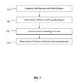
- FIG. 1shows a flow chart of a process for forming a dielectric film according to disclosed embodiments.
- FIG. 2shows another flow chart of a process for forming a dielectric film according to disclosed embodiments.
- FIG. 3Ashows a schematic cross-sectional view of a portion of a substrate processing chamber according to the disclosed technology.
- FIG. 3Bshows a bottom plan view of a showerhead according to the disclosed technology.
- FIG. 4shows a top plan view of an exemplary substrate processing system according to the disclosed technology.
- the present technologyincludes improved processes and chemistry profiles for depositing silicon-based materials on substrates. While conventional processes may deposit films of similar materials, the films may suffer from reduced quality and density. Accordingly, when lower quality films are densified to produce a higher quality film, film shrinkage may occur that may have an adverse effect on the underlying device. For example, as device geometries are reduced, the silicon or device base may have thinner wall profiles. When a film is deposited within the structures and densified, the shrinking film may exert stress on the underlying structures that can deform the patterning. The present technology, however, may form flowable films that fundamentally shrink less than conventional films. In so doing, more intricate patterns can be covered.
- trenches within the devicemay have very high aspect ratios, such as having a height:width ratio greater than or about 5:1, 8:1, 10:1, etc. or more, and as such a flowable dielectric film may be required to provide a bottom-up fill profile. If these films also shrink less when densified, less stress is exerted on the underlying structure, and overall process quality may be improved.
- Methods of forming a dielectric layer on a substratemay include introducing a first precursor into a remote plasma region fluidly coupled with a substrate processing region of a substrate processing chamber
- a plasmamay be formed in the remote plasma region to produce plasma effluents.
- the plasma effluentsmay be directed into the substrate processing region.
- a silicon-containing precursormay be introduced into the substrate processing region, and the silicon-containing precursor may include at least one silicon-silicon bond.
- the plasma effluents and silicon-containing precursormay be reacted in the processing region to form a silicon-based dielectric layer that is initially flowable when formed on the substrate.
- Precursors used in deposition of silicon-based filmsmay include a variety of additional molecules that affect the quality of the deposited film. For example, the presence of hydroxyl groups may increase the flowability of a deposited film. However, it may be desirable to remove these groups in the final film to produce higher quality films. The removal of these groups, or the substitution with other materials including oxygen, nitrogen, and carbon, for example, may reduce the overall density of the deposited or formed film. Accordingly, when later processing steps used to densify the film are performed, the film may shrink, which may produce unwanted stresses on the underlying structure. The inventors have advantageously determined that by reducing the inclusion of materials beyond silicon in the utilized precursors, the resulting film may have improved quality and may have reduced shrinking as compared to conventional films based on more varied precursor groups.
- FIG. 1shows a flow chart of a process for forming a dielectric film according to disclosed embodiments.
- a substratePrior to the first operation, a substrate may be delivered into a process chamber, such as those described below. The substrate may be previously patterned or relatively clean.
- Various front end processingmay have been performed including the formation of gates, vias, trenches, and other structures. These structures may be on the nanometer scale, and for example, trenches or gaps that require filling may have widths of less than about 100 nm, and may alternatively be less than or about 75 nm, 50 nm, 40 nm, 30 nm, 25 nm, 20 nm, 10 nm, etc. or less.
- the patterned substratemay then be delivered to a substrate processing region for deposition of a dielectric material.
- the substratemay already be located in the processing region if a previous operation was performed in the same chamber in which the deposition process is to occur.
- a first precursormay be introduced into a plasma region of the processing chamber that is separate or removed from the processing region of the chamber in which the substrate resides.
- the first precursormay include one of several precursor materials.
- the first precursormay be one or more inert gases including argon, helium, nitrogen, etc. Additional gases may alternatively or additionally be used, and may include ammonia (NH 3 ), hydrogen, or nitrogen and/or hydrogen-containing gases.
- the first precursormay exclusively include inert gases, and in an exemplary process argon or helium is delivered to the plasma region.
- the separate plasma regionmay be referred to as a remote plasma region herein and may be within a distinct module separate from the processing chamber, or as a compartment within the processing chamber.
- a plasmamay be formed within the remote plasma region thereby generating plasma effluents from the first precursor.
- the generated plasma effluentsare directed into the substrate processing region. This may be effected in a number of ways, including with a pressure differential, generated electric field, or some other known mechanism for directing the flow of ions and/or electrons into the processing region.
- a silicon-containing precursormay be introduced into the substrate processing region.
- the silicon-containing precursorincludes at least one silicon-silicon bond.
- the plasma effluents and silicon-containing precursormay be reacted in the substrate processing region to form a silicon based dielectric layer on the substrate.
- the formed materialmay be initially flowable when formed or when deposited initially, which may allow the material to flow down into trenches to fill defined patterns on the substrate.
- the dielectric materialmay be based on reactions between the plasma species and the silicon-containing precursor.
- the precursorsmay begin reacting directly upon contacting one another, and accordingly the precursors may be separated until entering the substrate processing region. Such separation may be performed by components such as a dual-channel showerhead as described further below.
- the showerheadmay be configured to maintain separation of the precursors so as to prevent the precursors from contacting one another until they enter or are delivered into the substrate processing region.
- the number of silicon-silicon bonds in the deposited filmmay directly correspond to the amount of shrinking of the produced film.
- the more silicon-silicon bonds in the filmthe less shrinking may occur as a result of densification because less additional polymerization may be imparted along with less removal of unwanted species.
- the formed filmmay be oxidized or reacted with additional material so as to incorporate oxygen into the polymer matrix, and remove residual materials such as hydrogen, nitrogen, carbon, etc.
- the more materials that are removed from the filmmay leave pores within the film that are removed during densification, such as annealing. The removal of these pores may compress the film imparting stress along surfaces contacted by the film.
- the present technologymay utilize silicon-containing precursors that maximize the number of silicon-silicon bonds, and minimize additional molecular bonding. In this way, less material may need to be removed during curing or other operations, which may reduce the amount of shrinking of the final film.
- the technologymay utilize silanes and polysilanes as the silicon-containing precursor.
- These materialsmay include or exclusively consist of silicon-silicon and silicon-hydrogen bonds.
- Exemplary precursorsmay include at least one silicon-silicon bond, at least two silicon-silicon bonds, at least three silicon-silicon bonds, etc.
- the precursorsmay be selected from any of the polysilane homologues beginning with disilane.
- the silicon-containing precursormay also be selected from a variety of isomers of the polysilanes.
- the compositioncould include any of n-pentasilane, isopentasilane, neopentasilane, 2-silyltetrasilane, 2,2-disilyltrisilane, etc.
- the silicon-containing precursorsmay include cyclic forms or cyclosilanes, such as cyclohexasilane, for example.
- the polysilanesmay also include any saturated or unsaturated compound such as silenes and silynes.
- the silicon-containing precursormay also be of a general formula such as Si x H y .
- Xmay be any number of two or greater up to infinity
- Ymay be any number of two or greater up to infinity.
- Ymay also be any factor based on X.
- Exemplary silanes used in the technologycan include disilane, tetrasilane, cyclohexasilane, etc.
- the vapor pressure of many of these disclosed materialsis such that the materials may be in a substantially liquid phase under many operating conditions.
- the silicon-containing precursorsmay be used in liquid form in the disclosed technology, in embodiments the silicon-containing precursors may be introduced into the processing chamber in a vapor or substantially vapor form. However, this may require the use of additional components to ensure that the materials are introduced in a vapor form.
- Many different mechanismsmay be employed to deliver vapor phase silicon-containing precursors. For example, vapor draw with or without a heated ampoule, a bubbler, or direct liquid injection may be utilized among a variety of other technology. However, depending on the precursor utilized, additional issues may occur.
- the injection nozzlemay be heated to deliver the material into the substrate processing region as a vapor.
- the vaporization temperature of higher order silanes and the polymerization temperature of higher order silanesmay be relatively close, such that the technique may clog the nozzle.
- a bubblermay utilize an inert gas in the delivery of the vapor, but also introduces the additional inert gas. In so doing, further mechanisms may be needed to ensure that an adequate flow of the actual silicon-containing precursor is delivered to provide adequate film formation rates.
- Higher order silicon-containing precursors or silaneshave more silicon-silicon bonds which may lead to less shrinking of the films, but may additionally have very low vapor pressures which may require additional components or mechanisms to provide a vapor phase silicon-containing precursor to the substrate processing region.
- flowability of the dielectric material with the disclosed technologymay be based on a combination of process parameters including the temperature and pressure of the process in relation to the silicon-containing precursor, plasma power used, and distance between the showerhead or mechanism delivering the precursors and the substrate on which the films are to be formed.
- the substrate processing regionmay be relatively, substantially, or completely plasma-free during the deposition.
- the plasma effluents of the first precursormay be delivered into the substrate processing region, the plasma used to generate the effluents may be contained externally to the substrate processing region. The greatest amount of reactions may occur directly under the showerhead, or where the precursors initially interact.
- the plasma effluentsmay have had the least amount of time to recombine, and thus greater reactions between the precursors may occur. These gas phase reactions may be affected further by the material used. Silicon-silicon bonds may be weaker bonds than silicon-hydrogen, silicon-oxygen, and other silicon-based bonds. Accordingly, where these greater reactions occur, or where a higher plasma power is utilized, for the silicon-containing precursors of the present technology, a greater number of bonds may be broken. As a possible result, the dielectric material formed in this region may have reduced or no flowability when deposited on the substrate. As the distance of the substrate from the showerhead increases, the amount of interactions may be reduced slightly or more substantially. For example, potentially only one out of two or one out of three silicon-silicon bonds may be broken, and thus the polymerization may include longer chains of silicon groups, which may at least partially impart flowability to the deposited material.
- the substratemay be maintained at a distance from the showerhead, or region where the interactions between the precursors begin, that is less than or about three inches.
- the substratemay be maintained at least 0.1 inches from the showerhead in disclosed embodiments.
- the substratemay also be maintained at a distance less than or about 2 inches, 1 inch, 0.9, 0.8, 0.7, 0.6, 0.5, 0.4, 0.3, 0.2, 0.1, or less inches, or be maintained between about 3 inches and about 0.01 inches, 2 and 0.1 inches, 1 and 0.2 inches, 0.8 and 0.2 inches, etc.
- the distancemay also be determined in conjunction with the process parameters and silicon-containing precursor or precursors being used.
- the substratemay be maintained at or below about 400° C., and may be maintained at or below about 300° C., 200° C., 100° C., 80° C., 75° C., 50° C., 25° C., 10° C., 0° C., ⁇ 10° C., ⁇ 20° C., ⁇ 30° C., or less, between about 30° C. and ⁇ 30° C., etc.
- the processing chambermay be maintained at or below about 100 Torr during the processes, and may be maintained at or below about 50 Torr, 25 Torr, 15 Torr, 5 Torr, 1 Torr, 0.1 Torr, etc., or between about 0.1 mTorr and about 10 Torr.
- the temperature and pressuremay also be set based at least partially on the vapor pressure of the silicon-containing precursor or precursors being used.
- the vapor pressure of tetrasilanemay be below about 3 Torr.
- the chamber pressureis greater than about 3 Torr, then condensation of the tetrasilane may occur.
- the interaction of the plasma effluents with the tetrasilanemay also impart energy that overcomes the condensation point.
- the amount of silicon-silicon bond breakingmay be reduced, which may allow longer polymer chains to be formed.
- the combination of improved polymerization, i.e. longer silicon-silicon chains, along with the benefit of operations at or near the condensation point of the precursorsmay at least partially impart flowability to the films.
- the processmay also create longer silicon polymer chains with reduced additional material, which may reduce the amount of shrinking of the final film.
- the plasma source used in the technologymay include plasma generated in the chamber, but remote from and fluidly coupled with the substrate processing region, or alternatively generated in a module separate from but fluidly coupled with the processing chamber.
- the plasmamay be from any known or later developed technology, and may produce plasma power between about 0 and 2000 Watts. In disclosed embodiments, the plasma power may be less than or about 1000 Watts, or about 500, 300, 250, 200, 150, 100, 80, 60, 40, 20 Watts, etc. or less.
- a synergistic combinationmay be produced where an amount of condensation and an amount of polymerization occur to produce flowable films from silicon-containing precursors that may only include silicon and hydrogen bonding.
- the resultant filmsmay have flowability when initially formed on the substrate, but may be composed of mostly silicon-silicon and silicon-hydrogen bonds. These films that may have more silicon atoms in the matrix, and more silicon-silicon bonding in the deposited film, may shrink less than conventional films.
- the inventorshave additionally determined that these films may have increased density as formed over conventional films.
- the as-deposited filmsmay have a density greater than or equal to about 1.2 g/cc.
- the filmsmay also have densities greater than or equal to about 1.3 g/cc, 1.4, 1.5, 1.6, 1.7, 1.8, 1.9, 2.0, 2.1, etc. or greater.
- additional processesmay be performed.
- One or more densifying operationsmay be performed to increase the quality of the dielectric material.
- the introduction and flow of the silicon-containing precursormay be stopped.
- the plasma effluentsmay be continued to be produced and directed into the substrate processing region at the formed dielectric layer to densify the formed dielectric material.
- the formed silicon-based dielectric layermay be annealed to further densify the film.
- the annealingmay be a dry anneal, such as with nitrogen, or a steam anneal that may occur at temperatures between about 200° C.
- the amount or film shrinkingmay be less than conventional films.
- the filmmay shrink by less than 50% during the anneal.
- the films produced by the disclosed technologymay shrink by less than or about 40%, 30%, 25%, 20%, 15%, 10%, 5%, 0%, ⁇ 5%, ⁇ 10%, etc. or less.
- the inventorshave determined that negative shrinking may occur. This negative shrinking may imply that the film expands during the processing.
- FIG. 2shows another flow chart of a process for forming a dielectric film according to disclosed embodiments. The process may include similar operations as described with respect to FIG. 1 .
- a first precursormay be introduced into a remote plasma region fluidly coupled with a substrate processing region while forming a plasma in the remote plasma region to produce plasma effluents.
- the first precursormay include one or more of any of the previously described precursors, and may consist exclusively of one or more inert precursors such as argon, helium, or nitrogen.
- the plasma effluentsmay be directed into the substrate processing region.
- a silicon-containing precursormay be introduced into the substrate processing region at operation 230 , and the silicon-containing precursor may have at least one silicon-silicon bond.
- the silicon-containing precursormay include one or more of any of the previously discussed precursors.
- the silicon-containing precursormay have the formula Si x H y , where x may be greater than or equal to 2, and y is 2x+n or greater, and where n may be any number less than or equal to 2.
- the silicon-containing precursormay be introduced into the processing region in a substantially vapor phase.
- the precursors introduced into the processing chamber to form the silicon-based dielectric layermay consist of one or more inert precursors and a silicon-containing precursor consisting or silicon-silicon and silicon-hydrogen containing bonds.
- the first precursormay consist of argon or helium.
- the plasma effluents and silicon-containing precursorsmay be reacted to form a silicon-based dielectric layer on the substrate. These operations may be performed in any of the ways previously described.
- a curing operationmay optionally be performed at operation 250 that cures the formed silicon-based dielectric layer with at least one additional precursor.
- the additional precursormay include one or more of an oxygen-containing precursor, such as ozone, a nitrogen-containing precursor, or a carbon-containing precursor.
- the precursorsmay be introduced or utilized with or without the plasma effluents directed into the substrate processing region.
- the additional precursorsmay be used to additionally substitute material into the silicon-based dielectric material.
- ozone or another oxygen-containing precursormay be used to provide oxygen that is incorporated into the silicon matrix to produce a silicon oxide film. This may help pack the formed matrix with additional material that may further help reduce shrinkage on annealing or densifying operations.
- a variety of filmsmay be formed in this way, including oxides, nitrides, carbides, oxycarbides, oxynitrides, carbonitrides, etc.
- the additional precursorsmay be flowed after the formation of the silicon-based dielectric, near the end of the formation, and may be introduced with or without the silicon-containing precursors and/or the first precursor.
- the temperature and/or pressure of the chambermay be changed during the curing operation. For example, if the temperature of the film forming operation is less than 30° C., for example, the chamber temperature may be raised to above or about 30° C., 50° C., 100° C., 200° C., etc., or higher.
- the cured or otherwise formed dielectricmay be optionally densified at operation 260 .
- the flow of the silicon-containing precursor and/or the additional precursormay be stopped, and then the flow of the first precursor may be performed, or continued in various embodiments.
- Plasma effluents developed from the first precursormay be directed into the substrate processing region to densify the formed or cured dielectric layer.
- the densifying operationmay be performed prior to the curing operation such that operation 260 is performed prior to operation 250 .
- Additional operationsmay be performed optionally in the process including an anneal at operation 270 .
- the formed, cured, and/or densified dielectricmay be annealed as previously discussed to improve the final quality of the film.
- Further post-deposition treatmentsmay be performed that may include one or more of a variety of operations including UV, e-beam, and other curing or annealing type operations.
- the silicon-based dielectric layermay shrink by less than or about 50%.
- the films produced by the disclosed technologymay shrink by less than or about 40%, 30%, 25%, 20%, 15%, 10%, 5%, etc. or less. All optional operations may be performed in the same or a different chamber than the film forming or deposition operation. By maintaining the substrate in a chamber without breaking vacuum, moisture and other effects on the formed film may be reduced or prevented.
- the technologyalso encompasses delivery of the silicon-containing precursor into the remote plasma region.
- the silicon-containing precursormay be activated by a direct plasma applied either in a remote region of the chamber, or alternatively in the processing region of the chamber, where the silicon-containing precursor is delivered to the area in which a plasma is developed.
- a silicon-containing precursormay be delivered into a processing region or a plasma region of a chamber and activated with a plasma, such as a type of plasma previously defined.
- the silicon-containing precursormay be delivered with additional fluids such as inert carriers that may include argon and may include hydrogen in disclosed embodiments as well.
- the processmay be performed at a variety of the temperatures, pressures, and plasma powers previously described.
- the plasma power applied directlymay be less than 500 W, and may also be less than or about 300 W, 200 W, 100 W, 80 W, 70 W, 60 W, 50 W, etc. or less, and the temperatures may be below or about 100° C., and may also be less than or about 75° C., 50° C., 25° C., 15° C., 10° C., 5° C., 0° C., ⁇ 5° C., etc. or less.
- the pedestal on which the substrate residesmay be electrically biased. Biasing of the pedestal may provide an electrical field that may be used to direct radical species to the surface of the substrate.
- the described processessynergistically utilize silicon-containing precursors having silicon-silicon bonding, temperature, pressure, plasma, and deposition distances to produce flowable films of improved qualities and reduced shrinking
- the technologyadvantageously may remove nitrogen, carbon, water, hydroxyl groups, and other additional materials that may reduce the density, and increase the shrinking of the formed films.
- additional modifications to chamber parameters and plasma powermay be used to further tune the deposition processes as may be required.
- tuning these processesmay be performed without the need to break vacuum conditions or move the substrate to an additional chamber. This may reduce overall processing times and save costs over conventional techniques. Additional examples of deposition process parameters, chemistries, and components are disclosed in the course of describing an exemplary processing chamber and system below.
- Deposition chambersmay include high-density plasma chemical vapor deposition (HDP-CVD) chambers, plasma enhanced chemical vapor deposition (PECVD) chambers, sub-atmospheric chemical vapor deposition (SACVD) chambers, and thermal chemical vapor deposition chambers, among other types of chambers.
- HDP-CVDhigh-density plasma chemical vapor deposition
- PECVDplasma enhanced chemical vapor deposition
- SACVDsub-atmospheric chemical vapor deposition
- thermal chemical vapor deposition chambersamong other types of chambers.
- Specific examples of CVD systemsinclude the CENTURA ULTIMA® HDP-CVD chambers/systems, and PRODUCER® PECVD chambers/systems, available from Applied Materials, Inc. of Santa Clara, Calif.
- Examples of substrate processing chambers that can be used with exemplary methods of the inventionmay include those shown and described in co-assigned U.S. Provisional Patent App. No. 60/803,499 to Lubomirsky et al, filed May 30, 2006, and titled “PROCESS CHAMBER FOR DIELECTRIC GAPFILL,” the entire contents of which is herein incorporated by reference for all purposes. Additional exemplary systems may include those shown and described in U.S. Pat. Nos. 6,387,207 and 6,830,624, which are also incorporated herein by reference for all purposes.
- FIG. 3Ashows a schematic cross-sectional view of a portion of a substrate processing chamber 301 according to the disclosed technology.
- a remote plasma system (RPS) 310may process a gas which then travels through a gas inlet assembly 311 .
- Two distinct gas supply channelsmay be present within the gas inlet assembly 311 .
- a first channel 312may carry a gas that passes through the remote plasma system (RPS) 310 , while a second channel 313 may bypass the RPS 310 .
- the first channel 312may be used for the process gas and the second channel 313 may be used for a treatment gas in disclosed embodiments.
- the lid or conductive top portion 321 and a perforated partition, such as showerhead 353are shown with an insulating ring 324 disposed between, which may allow an AC potential to be applied to the lid 321 relative to showerhead 353 .
- the process gasmay travel through first channel 312 into chamber plasma region 320 and may be excited by a plasma in chamber plasma region 320 alone or in combination with RPS 310 .
- the combination of chamber plasma region 320 and/or RPS 310may be referred to as a remote plasma system herein.
- the perforated partition or showerhead 353may separate chamber plasma region 320 from a substrate processing region 370 beneath showerhead 353 .
- showerhead 353may allow a plasma present in chamber plasma region 320 to avoid directly exciting gases in substrate processing region 370 , while still allowing excited species to travel from chamber plasma region 320 into substrate processing region 370 .
- showerhead 353may be positioned between chamber plasma region 320 and substrate processing region 370 and allow plasma effluents or excited derivatives of precursors or other gases created within chamber plasma region 320 to pass through a plurality of through-holes 356 that traverse the thickness of the plate or plates included in the showerhead.
- the showerhead 353may also have one or more hollow volumes 351 that can be filled with a precursor in the form of a vapor or gas, such as a silicon-containing precursor, and pass through small holes 355 into substrate processing region 370 , but not directly into chamber plasma region 320 .
- showerhead 353may be thicker than the length of the smallest diameter 350 of the through-holes 356 in disclosed embodiments.
- the length 326 of the smallest diameter 350 of the through-holesmay be restricted by forming larger diameter portions of through-holes 356 part way through the showerhead 353 .
- the length of the smallest diameter 350 of the through-holes 356may be the same order of magnitude as the smallest diameter of the through-holes 356 or less in disclosed embodiments.
- showerhead 353may distribute, via through-holes 356 , process gases which contain a plasma vapor/gas such as argon, for example. Additionally, the showerhead 353 may distribute, via smaller holes 355 , a silicon-containing precursor that is maintained separately from the plasma region 320 . The process gas or gases and the silicon-containing precursor may be maintained fluidly separate via the showerhead 353 until the precursors separately enter the processing region 370 . The precursors may contact one another once they enter the processing region and react to form a flowable dielectric material on a substrate 380 .
- process gaseswhich contain a plasma vapor/gas such as argon, for example.
- the showerhead 353may distribute, via smaller holes 355 , a silicon-containing precursor that is maintained separately from the plasma region 320 .
- the process gas or gases and the silicon-containing precursormay be maintained fluidly separate via the showerhead 353 until the precursors separately enter the processing region 370 .
- the precursorsmay contact one another once they enter the processing region and react to form
- the number of through-holes 356may be between about 60 and about 2000.
- Through-holes 356may have a variety of shapes but may be made round.
- the smallest diameter 350 of through-holes 356may be between about 0.5 mm and about 20 mm or between about 1 mm and about 6 mm in disclosed embodiments.
- the number of small holes 355 used to introduce a gas into substrate processing region 370may be between about 100 and about 5000 or between about 500 and about 2000 in different embodiments.
- the diameter of the small holes 355may be between about 0.1 mm and about 2 mm.
- FIG. 3Bshows a bottom plan view of a showerhead 353 according to the disclosed technology.
- showerhead 353corresponds with the showerhead shown in FIG. 3A .
- Through-holes 356are depicted with a larger inner-diameter (ID) on the bottom of showerhead 353 and a smaller ID at the top.
- Small holes 355are distributed substantially evenly over the surface of the showerhead, even amongst the through-holes 356 which may help to provide more even mixing than other embodiments described herein.
- An exemplary filmmay be created on a substrate supported by a pedestal, such as pedestal 375 having a substrate 380 disposed thereon, within substrate processing region 370 when plasma effluents arriving through through-holes 356 in showerhead 353 combine with a silicon-containing precursor arriving through the small holes 355 originating from hollow volumes 351 .
- substrate processing region 370may be equipped to support a plasma for other processes such as curing, no plasma may be present during the growth or deposition of the exemplary films.
- a plasmamay be ignited either in chamber plasma region 320 above showerhead 353 or substrate processing region 370 below showerhead 353 .
- no plasmamay be formed in any portion of the chamber, and may be only formed in RPS unit 310 .
- a plasmamay be present in chamber plasma region 320 to produce the radical plasma effluents, such as from an inflow of one or more of argon, helium, hydrogen, or ammonia.
- An AC voltage typically in the radio frequency (RF) rangeis applied between the conductive top portion, such as lid 321 , of the processing chamber and showerhead 353 to ignite a plasma in chamber plasma region 320 during deposition.
- An RF power supplygenerates a high RF frequency of 13.56 MHz but may also generate other frequencies alone or in combination with the 13.56 MHz frequency.
- the top plasmamay be left at low or no power when the bottom plasma in the substrate processing region 370 may be turned on during the formation of the dielectric layer or while cleaning the interior surfaces bordering substrate processing region 370 .
- a plasma in substrate processing region 370may be ignited by applying an AC voltage between showerhead 353 and the pedestal 375 or bottom of the chamber.
- a cleaning gasmay be introduced into substrate processing region 370 while the plasma is present.
- the pedestal 375may be moveable, and may be configured to be raised or lowered in disclosed embodiments, and may similarly be configured to rotate.
- the pedestal 375may have a heat exchange channel through which a heat exchange fluid flows to control the temperature of the substrate. This configuration allows the substrate temperature to be cooled or heated to maintain relatively low temperatures, such as from about 0° C. or lower up to about 200° C. or higher.
- the heat exchange fluidmay comprise ethylene glycol, water, or some other fluid capable of introducing or removing heat from the system.
- the wafer support platter of the pedestalmay also be resistively heated in order to achieve relatively high temperatures from about 200° C. or lower up to about 1100° C. or higher using an embedded resistive heating element.
- An outer portion of the heater elementmay run adjacent to a perimeter of the support platter, while an inner portion runs on the path of a concentric circle having a smaller radius.
- the resistive heating elementmay additionally be coiled through the platter to provide more uniform temperatures.
- the wiring to the heater elementmay pass through the stem of the pedestal.
- the chamber plasma region or a region in an RPSmay be referred to as a remote plasma region.
- the radical precursore.g. an argon precursor
- the silicon-containing precursoris excited only by the radical-argon precursor.
- Plasma powermay essentially be applied only to the remote plasma region, in embodiments, to ensure that the radical-argon precursor provides the dominant excitation to the silicon-containing precursor.
- the excited plasma effluentsmay be generated in a section of the substrate processing region partitioned from a deposition region.
- the deposition regionalso known herein as the substrate processing region, may be where the plasma effluents mix and react with the silicon-containing precursor to deposit dielectric material on the substrate, e.g., a semiconductor wafer.
- the excited plasma effluentsmay also be accompanied by additional gases including other inert gases or ammonia, for example.
- the silicon-containing precursormay not pass through a plasma before entering the substrate plasma region, in embodiments.
- the substrate processing regionmay be described herein as “plasma-free” during the deposition of the dielectric material.
- “Plasma-free”does not necessarily mean the region is devoid of plasma. Ionized species and free electrons created within the plasma region may travel through pores or apertures in the partition or showerhead, but the silicon-containing precursor may not be substantially excited by the plasma power applied to the plasma region. The borders of the plasma in the chamber plasma region are hard to define and may encroach upon the substrate processing region through the apertures in the showerhead. In the case of an inductively-coupled plasma, a small amount of ionization may be effected within the substrate processing region directly. Furthermore, a low intensity plasma may be created in the substrate processing region without eliminating desirable features of the forming film. All causes for a plasma having much lower intensity ion density than the chamber plasma region, or a remote plasma region, during the creation of the excited plasma effluents do not deviate from the scope of “plasma-free” as used herein.
- Plasma powercan be a variety of frequencies or a combination of multiple frequencies.
- the plasmamay be provided by RF power delivered to lid 321 relative to showerhead 353 .
- the RF powermay be between about 10 watts and about 2000 watts, between about 100 watts and about 2000 watts, between about 200 watts and about 1500 watts, less than or about 100 Watts, or less than or about 500 watts in different embodiments.
- the RF frequency applied in the exemplary processing systemmay be low RF frequencies less than about 200 kHz, high RF frequencies between about 10 MHz and about 15 MHz, or microwave frequencies greater than or about 1 GHz in different embodiments.
- the plasma powermay be capacitively-coupled (CCP) or inductively-coupled (ICP) into the remote plasma region.
- CCPcapacitively-coupled
- ICPinductively-coupled
- Substrate processing region 370can be maintained at a variety of pressures during the flow of precursors, any carrier gases, and plasma effluents into substrate processing region 370 .
- the pressuremay be maintained between about 0.1 mTorr and about 100 Torr, between about 1 Torr and about 20 Torr, less than about 5 Torr, or less than about 3 Torr in different embodiments.
- FIG. 3shows one such system 400 of deposition, etching, baking, and curing chambers according to disclosed embodiments.
- a pair of front opening unified pods (FOUPs) 402supply substrates of a variety of sizes that are received by robotic arms 404 and placed into a low pressure holding area 406 before being placed into one of the substrate processing chambers 408 a - f .
- a second robotic arm 410may be used to transport the substrate wafers from the holding area 406 to the substrate processing chambers 408 a - f and back.
- Each substrate processing chamber 408 a - fcan be outfitted to perform a number of substrate processing operations including the deposition processes described herein in addition to cyclical layer deposition (CLD), atomic layer deposition (ALD), chemical vapor deposition (CVD), physical vapor deposition (PVD), etch, pre-clean, degas, orientation, and other substrate processes.
- CLDcyclical layer deposition
- ALDatomic layer deposition
- CVDchemical vapor deposition
- PVDphysical vapor deposition
- etchpre-clean, degas, orientation, and other substrate processes.
- the substrate processing chambers 408 a - fmay include one or more system components for depositing, annealing, curing and/or etching a dielectric film on the substrate wafer.
- two pairs of the processing chamberse.g., 408 c - d and 408 e - f
- the third pair of processing chamberse.g., 408 a - b
- all three pairs of chamberse.g., 408 a - f
- Any one or more of the processes describedmay be carried out in chamber(s) separated from the fabrication system shown in different embodiments.
Landscapes
- Chemical & Material Sciences (AREA)
- Engineering & Computer Science (AREA)
- Physics & Mathematics (AREA)
- Chemical Kinetics & Catalysis (AREA)
- Materials Engineering (AREA)
- General Chemical & Material Sciences (AREA)
- Organic Chemistry (AREA)
- Metallurgy (AREA)
- Mechanical Engineering (AREA)
- Manufacturing & Machinery (AREA)
- General Physics & Mathematics (AREA)
- Condensed Matter Physics & Semiconductors (AREA)
- Computer Hardware Design (AREA)
- Power Engineering (AREA)
- Microelectronics & Electronic Packaging (AREA)
- Plasma & Fusion (AREA)
- Inorganic Chemistry (AREA)
- Chemical Vapour Deposition (AREA)
- Formation Of Insulating Films (AREA)
Abstract
Description
This application claims the benefit of U.S. Provisional Application No. 61/756,762, filed Jan. 25, 2013, entitled “Low Shrinkage Dielectric Films.” The entire disclosure of which is incorporated herein by reference for all purposes.
The present technology relates to semiconductor processes and equipment. More specifically, the present technology relates to forming dielectric materials.
As integrated circuit chipmakers continue increasing the density of circuit elements on each chip, filling the gaps that separate those elements becomes more challenging. The increased circuit element density has necessitated shorter widths between adjacent elements. As the width of these gaps shrink faster than their height, the ratio of height to width (known as the aspect ratio) proportionally increases. It is more difficult to fill a tall and narrow gap (i.e., a high aspect ratio gap) with a uniform film of dielectric material than a shallow and wide gap (i.e., a low aspect ratio gap).
One commonly encountered difficulty with filling high aspect ratio gaps is the formation of voids. In high aspect ratio gaps, there is a tendency of the dielectric material filling the gap to deposit at a faster rate around the top end of the gap. Often the dielectric material will close the top before the gap has been completely filled, leaving a void. Even when the top of the gap does not close prematurely, the uneven growth rate of the dielectric film down the sidewalls of the gap can create a weak seam in the middle of the gapfill. These seams can later result in cracks that adversely affect the physical integrity and dielectric properties of the device.
One technique to avoid the formation of voids and weak seams in dielectric gapfills is to fill the gap at a lower deposition rate. Lower deposition rates can give the dielectric material more time to redistribute on the inside surfaces of the gap to reduce the chances of excessive topside growth. A lower deposition rate may also be the result of increased etching or sputtering that occur at the same time as the dielectric deposition. For example, in HDPCVD dielectric material at the top corners of the gap etch away faster than material on the sidewalls and bottom portion of the gap. This increases the chances that the topside of the gap will remain open so the sidewalls and bottom can completely fill with dielectric material. However, reducing the dielectric deposition rate also results in the deposition taking longer to complete. The longer deposition times decrease the rate at which substrate wafers are processed through the deposition chamber, resulting in a reduced efficiency for chamber.
Thus, there is a need for improved systems and methods for filling short-width, high aspect ratio gaps with a void free dielectric film. These and other problems are addressed by the systems and methods of the present invention.
Methods of forming a dielectric layer on a substrate are described, and may include introducing a first precursor into a remote plasma region fluidly coupled with a substrate processing region of a substrate processing chamber A plasma may be formed in the remote plasma region to produce plasma effluents. The plasma effluents may be directed into the substrate processing region. A silicon-containing precursor may be introduced into the substrate processing region, and the silicon-containing precursor may include at least one silicon-silicon bond. The plasma effluents and silicon-containing precursor may be reacted in the processing region to form a silicon-based dielectric layer that is initially flowable when formed on the substrate.
The silicon-containing precursors may include at least two silicon-silicon bonds, and may include three or more. The first precursor may include one or more precursors selected from the group including ammonia, nitrogen, H2, Ar, and He, and may include additional carrier gases or combinations of precursors as well. The plasma effluents and silicon-containing precursor may be introduced into the processing region through a showerhead configured to maintain separation of the precursors so that they do not contact each other until they enter the substrate processing region. The substrate may be maintained at a distance less than or at about 3 inches from the showerhead, and may be maintained closer or further away in disclosed embodiments. The substrate processing region may be plasma-free during the deposition process, and in alternative arrangements a direct plasma may be provided within the processing region.
The silicon-containing precursor may have the formula SixHy, where x is greater than or equal to 2, and y is 2x+n or greater, where n is any number less than or equal to 2. The silicon-containing precursor may also be introduced into the processing region in a substantially vapor phase. The method for deposition may be performed at a temperature of less than or equal to about 30° C., and the pressure during the process may be less than or equal to about 5 Torr. The as-formed film produced by the described processes may have a density greater than or equal to about 1.4 g/cc.
The methods may also include stopping the introduction of the silicon-containing precursor after the silicon-based dielectric layer is formed. The plasma effluents may be continuously directed into the substrate processing region, however, in order to densify the formed dielectric layer. The methods may further include annealing the formed silicon-based dielectric layer, and during the anneal, the formed silicon-based dielectric layer may shrink by less than about 20%.
Methods are also described for forming a dielectric layer on a substrate in a substrate processing region of a processing chamber. The methods may include introducing a first precursor into a remote plasma region fluidly coupled with the substrate processing region while forming a plasma in the remote plasma region to produce plasma effluents. The methods may also include directing the plasma effluents into the substrate processing region, and introducing a silicon-containing precursor into the substrate processing region. The silicon-containing precursor may include at least one silicon-silicon bond in disclosed embodiments. The methods may also include reacting the plasma effluents and silicon-containing precursor in the substrate processing region to form a silicon-based dielectric layer that is initially flowable when formed on the substrate. The methods may further include curing the formed silicon-based dielectric layer with at least one additional precursor.
The at least one additional precursor utilized may include an oxygen-containing precursor, a nitrogen-containing precursor, or a carbon-containing precursor. The methods may also include directing the plasma effluents into the substrate processing region to densify the cured dielectric layer. The silicon-containing precursor utilized may have the formula SixHy, where x is greater than or equal to 2, and y is 2x+n or greater, where n is any number less than or equal to 2, and where the silicon-containing precursor is introduced into the processing region in a substantially vapor phase. The precursors introduced into the processing chamber to form the silicon-based dielectric layer may include one or more inert precursors and a silicon-containing precursor having silicon-silicon and silicon-hydrogen containing bonds. The methods may also include the step of annealing the formed silicon-based dielectric layer. When performed, the annealing may shrink the formed dielectric layer by less than about 20% during the annealing.
Such technology may provide numerous benefits over conventional techniques. For example, the deposition processes disclosed may produce denser and higher quality films. As such, film shrinkage may be reduced or prevented during annealing or post-formation operations. These and other embodiments, along with many of their advantages and features, are described in more detail in conjunction with the below description and attached figures.
A further understanding of the nature and advantages of the disclosed technology may be realized by reference to the remaining portions of the specification and the drawings.
In the appended figures, similar components and/or features may have the same numerical reference label. Further, various components of the same type may be distinguished by following the reference label by a letter that distinguishes among the similar components and/or features. If only the first numerical reference label is used in the specification, the description is applicable to any one of the similar components and/or features having the same first numerical reference label irrespective of the letter suffix.
The present technology includes improved processes and chemistry profiles for depositing silicon-based materials on substrates. While conventional processes may deposit films of similar materials, the films may suffer from reduced quality and density. Accordingly, when lower quality films are densified to produce a higher quality film, film shrinkage may occur that may have an adverse effect on the underlying device. For example, as device geometries are reduced, the silicon or device base may have thinner wall profiles. When a film is deposited within the structures and densified, the shrinking film may exert stress on the underlying structures that can deform the patterning. The present technology, however, may form flowable films that fundamentally shrink less than conventional films. In so doing, more intricate patterns can be covered. For example, trenches within the device may have very high aspect ratios, such as having a height:width ratio greater than or about 5:1, 8:1, 10:1, etc. or more, and as such a flowable dielectric film may be required to provide a bottom-up fill profile. If these films also shrink less when densified, less stress is exerted on the underlying structure, and overall process quality may be improved.
Methods of forming a dielectric layer on a substrate are described, and may include introducing a first precursor into a remote plasma region fluidly coupled with a substrate processing region of a substrate processing chamber A plasma may be formed in the remote plasma region to produce plasma effluents. The plasma effluents may be directed into the substrate processing region. A silicon-containing precursor may be introduced into the substrate processing region, and the silicon-containing precursor may include at least one silicon-silicon bond. The plasma effluents and silicon-containing precursor may be reacted in the processing region to form a silicon-based dielectric layer that is initially flowable when formed on the substrate.
Precursors used in deposition of silicon-based films may include a variety of additional molecules that affect the quality of the deposited film. For example, the presence of hydroxyl groups may increase the flowability of a deposited film. However, it may be desirable to remove these groups in the final film to produce higher quality films. The removal of these groups, or the substitution with other materials including oxygen, nitrogen, and carbon, for example, may reduce the overall density of the deposited or formed film. Accordingly, when later processing steps used to densify the film are performed, the film may shrink, which may produce unwanted stresses on the underlying structure. The inventors have advantageously determined that by reducing the inclusion of materials beyond silicon in the utilized precursors, the resulting film may have improved quality and may have reduced shrinking as compared to conventional films based on more varied precursor groups.
In order to better understand and appreciate the invention, reference is now made toFIG. 1 , which shows a flow chart of a process for forming a dielectric film according to disclosed embodiments. Prior to the first operation, a substrate may be delivered into a process chamber, such as those described below. The substrate may be previously patterned or relatively clean. Various front end processing may have been performed including the formation of gates, vias, trenches, and other structures. These structures may be on the nanometer scale, and for example, trenches or gaps that require filling may have widths of less than about 100 nm, and may alternatively be less than or about 75 nm, 50 nm, 40 nm, 30 nm, 25 nm, 20 nm, 10 nm, etc. or less. The patterned substrate may then be delivered to a substrate processing region for deposition of a dielectric material. In disclosed embodiments, the substrate may already be located in the processing region if a previous operation was performed in the same chamber in which the deposition process is to occur. Atoperation 110, a first precursor may be introduced into a plasma region of the processing chamber that is separate or removed from the processing region of the chamber in which the substrate resides. The first precursor may include one of several precursor materials. For example, the first precursor may be one or more inert gases including argon, helium, nitrogen, etc. Additional gases may alternatively or additionally be used, and may include ammonia (NH3), hydrogen, or nitrogen and/or hydrogen-containing gases. In disclosed embodiments, the first precursor may exclusively include inert gases, and in an exemplary process argon or helium is delivered to the plasma region.
The separate plasma region may be referred to as a remote plasma region herein and may be within a distinct module separate from the processing chamber, or as a compartment within the processing chamber. A plasma may be formed within the remote plasma region thereby generating plasma effluents from the first precursor. Atoperation 120, the generated plasma effluents are directed into the substrate processing region. This may be effected in a number of ways, including with a pressure differential, generated electric field, or some other known mechanism for directing the flow of ions and/or electrons into the processing region. Before, after, or concurrently withoperation 120, a silicon-containing precursor may be introduced into the substrate processing region. In disclosed embodiments, the silicon-containing precursor includes at least one silicon-silicon bond.
The plasma effluents and silicon-containing precursor may be reacted in the substrate processing region to form a silicon based dielectric layer on the substrate. The formed material may be initially flowable when formed or when deposited initially, which may allow the material to flow down into trenches to fill defined patterns on the substrate. The dielectric material may be based on reactions between the plasma species and the silicon-containing precursor. The precursors may begin reacting directly upon contacting one another, and accordingly the precursors may be separated until entering the substrate processing region. Such separation may be performed by components such as a dual-channel showerhead as described further below. The showerhead may be configured to maintain separation of the precursors so as to prevent the precursors from contacting one another until they enter or are delivered into the substrate processing region. Previous technologies may have relied on the inclusion of water or hydroxyl groups in the as deposited film to potentially impart the flowability of the film. As previously stated, though, these groups may produce weaker films that may shrink unacceptably upon densification. The present technology, however, utilizes a variety of parameters that may synergistically allow flowability to occur.
Without being bound to a particular theory, the number of silicon-silicon bonds in the deposited film may directly correspond to the amount of shrinking of the produced film. For example, the more silicon-silicon bonds in the film, the less shrinking may occur as a result of densification because less additional polymerization may be imparted along with less removal of unwanted species. Such as when a silicon oxide film is being formed, after the initial deposition, the formed film may be oxidized or reacted with additional material so as to incorporate oxygen into the polymer matrix, and remove residual materials such as hydrogen, nitrogen, carbon, etc. The more materials that are removed from the film may leave pores within the film that are removed during densification, such as annealing. The removal of these pores may compress the film imparting stress along surfaces contacted by the film. These stresses may overcome a threshold that allows the structure to deform, which may destroy the underlying structure. Accordingly, the present technology may utilize silicon-containing precursors that maximize the number of silicon-silicon bonds, and minimize additional molecular bonding. In this way, less material may need to be removed during curing or other operations, which may reduce the amount of shrinking of the final film.
In disclosed embodiments, the technology may utilize silanes and polysilanes as the silicon-containing precursor. These materials may include or exclusively consist of silicon-silicon and silicon-hydrogen bonds. Exemplary precursors may include at least one silicon-silicon bond, at least two silicon-silicon bonds, at least three silicon-silicon bonds, etc. For example, the precursors may be selected from any of the polysilane homologues beginning with disilane. The silicon-containing precursor may also be selected from a variety of isomers of the polysilanes. For example, if the silicon-containing precursor has five silicon atoms, the composition could include any of n-pentasilane, isopentasilane, neopentasilane, 2-silyltetrasilane, 2,2-disilyltrisilane, etc. The silicon-containing precursors may include cyclic forms or cyclosilanes, such as cyclohexasilane, for example. The polysilanes may also include any saturated or unsaturated compound such as silenes and silynes. The silicon-containing precursor may also be of a general formula such as SixHy. X may be any number of two or greater up to infinity, and Y may be any number of two or greater up to infinity. For example, such a minimal formula would denote disilyne (Si2H2). Y may also be any factor based on X. For example, Y may be 2X, or 2X+N, where n=2, 0, −2, −4, −6, etc., or N may be any number less than or equal to 2. Exemplary silanes used in the technology can include disilane, tetrasilane, cyclohexasilane, etc.
The vapor pressure of many of these disclosed materials is such that the materials may be in a substantially liquid phase under many operating conditions. Although the silicon-containing precursors may be used in liquid form in the disclosed technology, in embodiments the silicon-containing precursors may be introduced into the processing chamber in a vapor or substantially vapor form. However, this may require the use of additional components to ensure that the materials are introduced in a vapor form. Many different mechanisms may be employed to deliver vapor phase silicon-containing precursors. For example, vapor draw with or without a heated ampoule, a bubbler, or direct liquid injection may be utilized among a variety of other technology. However, depending on the precursor utilized, additional issues may occur. For example, if higher order silanes are delivered in liquid phase to an injection nozzle, the injection nozzle may be heated to deliver the material into the substrate processing region as a vapor. However, the vaporization temperature of higher order silanes and the polymerization temperature of higher order silanes may be relatively close, such that the technique may clog the nozzle. Additionally, a bubbler may utilize an inert gas in the delivery of the vapor, but also introduces the additional inert gas. In so doing, further mechanisms may be needed to ensure that an adequate flow of the actual silicon-containing precursor is delivered to provide adequate film formation rates. Higher order silicon-containing precursors or silanes have more silicon-silicon bonds which may lead to less shrinking of the films, but may additionally have very low vapor pressures which may require additional components or mechanisms to provide a vapor phase silicon-containing precursor to the substrate processing region.
Again without being bound to any particular theory, flowability of the dielectric material with the disclosed technology may be based on a combination of process parameters including the temperature and pressure of the process in relation to the silicon-containing precursor, plasma power used, and distance between the showerhead or mechanism delivering the precursors and the substrate on which the films are to be formed. During the processing, the substrate processing region may be relatively, substantially, or completely plasma-free during the deposition. Although the plasma effluents of the first precursor may be delivered into the substrate processing region, the plasma used to generate the effluents may be contained externally to the substrate processing region. The greatest amount of reactions may occur directly under the showerhead, or where the precursors initially interact. The plasma effluents may have had the least amount of time to recombine, and thus greater reactions between the precursors may occur. These gas phase reactions may be affected further by the material used. Silicon-silicon bonds may be weaker bonds than silicon-hydrogen, silicon-oxygen, and other silicon-based bonds. Accordingly, where these greater reactions occur, or where a higher plasma power is utilized, for the silicon-containing precursors of the present technology, a greater number of bonds may be broken. As a possible result, the dielectric material formed in this region may have reduced or no flowability when deposited on the substrate. As the distance of the substrate from the showerhead increases, the amount of interactions may be reduced slightly or more substantially. For example, potentially only one out of two or one out of three silicon-silicon bonds may be broken, and thus the polymerization may include longer chains of silicon groups, which may at least partially impart flowability to the deposited material.
Accordingly, the substrate may be maintained at a distance from the showerhead, or region where the interactions between the precursors begin, that is less than or about three inches. The substrate may be maintained at least 0.1 inches from the showerhead in disclosed embodiments. The substrate may also be maintained at a distance less than or about 2 inches, 1 inch, 0.9, 0.8, 0.7, 0.6, 0.5, 0.4, 0.3, 0.2, 0.1, or less inches, or be maintained between about 3 inches and about 0.01 inches, 2 and 0.1 inches, 1 and 0.2 inches, 0.8 and 0.2 inches, etc. The distance may also be determined in conjunction with the process parameters and silicon-containing precursor or precursors being used.
During the deposition process, the substrate may be maintained at or below about 400° C., and may be maintained at or below about 300° C., 200° C., 100° C., 80° C., 75° C., 50° C., 25° C., 10° C., 0° C., −10° C., −20° C., −30° C., or less, between about 30° C. and −30° C., etc. The processing chamber may be maintained at or below about 100 Torr during the processes, and may be maintained at or below about 50 Torr, 25 Torr, 15 Torr, 5 Torr, 1 Torr, 0.1 Torr, etc., or between about 0.1 mTorr and about 10 Torr. The temperature and pressure may also be set based at least partially on the vapor pressure of the silicon-containing precursor or precursors being used. As one non-limiting example, if tetrasilane is used as the silicon-containing precursor, and the chamber temperature is about −10° C., the vapor pressure of tetrasilane may be below about 3 Torr. As such, if the chamber pressure is greater than about 3 Torr, then condensation of the tetrasilane may occur. The interaction of the plasma effluents with the tetrasilane may also impart energy that overcomes the condensation point. Additionally, as the distance from the plasma source increases, and the plasma power decreases either or both from distance or actual generation power, the amount of silicon-silicon bond breaking may be reduced, which may allow longer polymer chains to be formed. The combination of improved polymerization, i.e. longer silicon-silicon chains, along with the benefit of operations at or near the condensation point of the precursors may at least partially impart flowability to the films. The process may also create longer silicon polymer chains with reduced additional material, which may reduce the amount of shrinking of the final film. The plasma source used in the technology may include plasma generated in the chamber, but remote from and fluidly coupled with the substrate processing region, or alternatively generated in a module separate from but fluidly coupled with the processing chamber. The plasma may be from any known or later developed technology, and may produce plasma power between about 0 and 2000 Watts. In disclosed embodiments, the plasma power may be less than or about 1000 Watts, or about 500, 300, 250, 200, 150, 100, 80, 60, 40, 20 Watts, etc. or less.
Utilizing the described processes, a synergistic combination may be produced where an amount of condensation and an amount of polymerization occur to produce flowable films from silicon-containing precursors that may only include silicon and hydrogen bonding. The resultant films may have flowability when initially formed on the substrate, but may be composed of mostly silicon-silicon and silicon-hydrogen bonds. These films that may have more silicon atoms in the matrix, and more silicon-silicon bonding in the deposited film, may shrink less than conventional films. Advantageously, the inventors have additionally determined that these films may have increased density as formed over conventional films. The as-deposited films may have a density greater than or equal to about 1.2 g/cc. The films may also have densities greater than or equal to about 1.3 g/cc, 1.4, 1.5, 1.6, 1.7, 1.8, 1.9, 2.0, 2.1, etc. or greater.
After an amount of dielectric material has been formed on the substrate, additional processes may be performed. One or more densifying operations may be performed to increase the quality of the dielectric material. In disclosed embodiments, once a determined amount of dielectric material has been formed, the introduction and flow of the silicon-containing precursor may be stopped. However, the plasma effluents may be continued to be produced and directed into the substrate processing region at the formed dielectric layer to densify the formed dielectric material. Additionally or alternatively, the formed silicon-based dielectric layer may be annealed to further densify the film. The annealing may be a dry anneal, such as with nitrogen, or a steam anneal that may occur at temperatures between about 200° C. and higher, above or about 400° C., above or about 900° C., etc. or greater. During the anneal, the amount or film shrinking may be less than conventional films. For example, the film may shrink by less than 50% during the anneal. Additionally, the films produced by the disclosed technology may shrink by less than or about 40%, 30%, 25%, 20%, 15%, 10%, 5%, 0%, −5%, −10%, etc. or less. In exemplary methods and processes, the inventors have determined that negative shrinking may occur. This negative shrinking may imply that the film expands during the processing.
The above example process as described in conjunction withFIG. 1 may produce a substantially silicon based film, and may be used to produce polysilicon films of various structure and characteristics. The processes may be further adjusted to incorporate additional materials to produce oxides, nitrides, carbides, and other compositions useful in semiconductor processing. A further example of the disclosed technology incorporating additional materials is described with respect toFIG. 2 .FIG. 2 shows another flow chart of a process for forming a dielectric film according to disclosed embodiments. The process may include similar operations as described with respect toFIG. 1 . In disclosed embodiments, at operation210 a first precursor may be introduced into a remote plasma region fluidly coupled with a substrate processing region while forming a plasma in the remote plasma region to produce plasma effluents. The first precursor may include one or more of any of the previously described precursors, and may consist exclusively of one or more inert precursors such as argon, helium, or nitrogen. Atoperation 220, the plasma effluents may be directed into the substrate processing region.
A silicon-containing precursor may be introduced into the substrate processing region atoperation 230, and the silicon-containing precursor may have at least one silicon-silicon bond. The silicon-containing precursor may include one or more of any of the previously discussed precursors. For example, the silicon-containing precursor may have the formula SixHy, where x may be greater than or equal to 2, and y is 2x+n or greater, and where n may be any number less than or equal to 2. Additionally, the silicon-containing precursor may be introduced into the processing region in a substantially vapor phase. In disclosed embodiments, the precursors introduced into the processing chamber to form the silicon-based dielectric layer may consist of one or more inert precursors and a silicon-containing precursor consisting or silicon-silicon and silicon-hydrogen containing bonds. For example, the first precursor may consist of argon or helium. Atoperation 240, the plasma effluents and silicon-containing precursors may be reacted to form a silicon-based dielectric layer on the substrate. These operations may be performed in any of the ways previously described. After the initial film has been formed, a curing operation may optionally be performed atoperation 250 that cures the formed silicon-based dielectric layer with at least one additional precursor.
The additional precursor may include one or more of an oxygen-containing precursor, such as ozone, a nitrogen-containing precursor, or a carbon-containing precursor. The precursors may be introduced or utilized with or without the plasma effluents directed into the substrate processing region. The additional precursors may be used to additionally substitute material into the silicon-based dielectric material. For example, ozone or another oxygen-containing precursor may be used to provide oxygen that is incorporated into the silicon matrix to produce a silicon oxide film. This may help pack the formed matrix with additional material that may further help reduce shrinkage on annealing or densifying operations. A variety of films may be formed in this way, including oxides, nitrides, carbides, oxycarbides, oxynitrides, carbonitrides, etc. The additional precursors may be flowed after the formation of the silicon-based dielectric, near the end of the formation, and may be introduced with or without the silicon-containing precursors and/or the first precursor. The temperature and/or pressure of the chamber may be changed during the curing operation. For example, if the temperature of the film forming operation is less than 30° C., for example, the chamber temperature may be raised to above or about 30° C., 50° C., 100° C., 200° C., etc., or higher.
Subsequent to the optional introduction of additional precursor material, the cured or otherwise formed dielectric may be optionally densified atoperation 260. The flow of the silicon-containing precursor and/or the additional precursor may be stopped, and then the flow of the first precursor may be performed, or continued in various embodiments. Plasma effluents developed from the first precursor may be directed into the substrate processing region to densify the formed or cured dielectric layer. In disclosed embodiments the densifying operation may be performed prior to the curing operation such thatoperation 260 is performed prior tooperation 250. Additional operations may be performed optionally in the process including an anneal atoperation 270. The formed, cured, and/or densified dielectric may be annealed as previously discussed to improve the final quality of the film. Further post-deposition treatments may be performed that may include one or more of a variety of operations including UV, e-beam, and other curing or annealing type operations. During the anneal, the silicon-based dielectric layer may shrink by less than or about 50%. The films produced by the disclosed technology may shrink by less than or about 40%, 30%, 25%, 20%, 15%, 10%, 5%, etc. or less. All optional operations may be performed in the same or a different chamber than the film forming or deposition operation. By maintaining the substrate in a chamber without breaking vacuum, moisture and other effects on the formed film may be reduced or prevented.
The technology also encompasses delivery of the silicon-containing precursor into the remote plasma region. Alternatively, the silicon-containing precursor may be activated by a direct plasma applied either in a remote region of the chamber, or alternatively in the processing region of the chamber, where the silicon-containing precursor is delivered to the area in which a plasma is developed. In disclosed embodiments, a silicon-containing precursor may be delivered into a processing region or a plasma region of a chamber and activated with a plasma, such as a type of plasma previously defined. The silicon-containing precursor may be delivered with additional fluids such as inert carriers that may include argon and may include hydrogen in disclosed embodiments as well. The process may be performed at a variety of the temperatures, pressures, and plasma powers previously described. For example, the plasma power applied directly may be less than 500 W, and may also be less than or about 300 W, 200 W, 100 W, 80 W, 70 W, 60 W, 50 W, etc. or less, and the temperatures may be below or about 100° C., and may also be less than or about 75° C., 50° C., 25° C., 15° C., 10° C., 5° C., 0° C., −5° C., etc. or less. Additionally, in this and other disclosed embodiments, the pedestal on which the substrate resides may be electrically biased. Biasing of the pedestal may provide an electrical field that may be used to direct radical species to the surface of the substrate.
The described processes synergistically utilize silicon-containing precursors having silicon-silicon bonding, temperature, pressure, plasma, and deposition distances to produce flowable films of improved qualities and reduced shrinking By accounting for the phase transition profiles of the silicon-containing precursors, the technology advantageously may remove nitrogen, carbon, water, hydroxyl groups, and other additional materials that may reduce the density, and increase the shrinking of the formed films. As would be understood, additional modifications to chamber parameters and plasma power may be used to further tune the deposition processes as may be required. Advantageously, tuning these processes may be performed without the need to break vacuum conditions or move the substrate to an additional chamber. This may reduce overall processing times and save costs over conventional techniques. Additional examples of deposition process parameters, chemistries, and components are disclosed in the course of describing an exemplary processing chamber and system below.
Exemplary Processing System
Deposition chambers that may implement embodiments of the present invention may include high-density plasma chemical vapor deposition (HDP-CVD) chambers, plasma enhanced chemical vapor deposition (PECVD) chambers, sub-atmospheric chemical vapor deposition (SACVD) chambers, and thermal chemical vapor deposition chambers, among other types of chambers. Specific examples of CVD systems that may implement embodiments of the invention include the CENTURA ULTIMA® HDP-CVD chambers/systems, and PRODUCER® PECVD chambers/systems, available from Applied Materials, Inc. of Santa Clara, Calif.
Examples of substrate processing chambers that can be used with exemplary methods of the invention may include those shown and described in co-assigned U.S. Provisional Patent App. No. 60/803,499 to Lubomirsky et al, filed May 30, 2006, and titled “PROCESS CHAMBER FOR DIELECTRIC GAPFILL,” the entire contents of which is herein incorporated by reference for all purposes. Additional exemplary systems may include those shown and described in U.S. Pat. Nos. 6,387,207 and 6,830,624, which are also incorporated herein by reference for all purposes.
In the embodiment shown,showerhead 353 may distribute, via through-holes 356, process gases which contain a plasma vapor/gas such as argon, for example. Additionally, theshowerhead 353 may distribute, viasmaller holes 355, a silicon-containing precursor that is maintained separately from theplasma region 320. The process gas or gases and the silicon-containing precursor may be maintained fluidly separate via theshowerhead 353 until the precursors separately enter theprocessing region 370. The precursors may contact one another once they enter the processing region and react to form a flowable dielectric material on asubstrate 380.
In embodiments, the number of through-holes 356 may be between about 60 and about 2000. Through-holes 356 may have a variety of shapes but may be made round. Thesmallest diameter 350 of through-holes 356 may be between about 0.5 mm and about 20 mm or between about 1 mm and about6mm in disclosed embodiments. There is also latitude in choosing the cross-sectional shape of through-holes, which may be made conical, cylindrical or a combination of the two shapes. The number ofsmall holes 355 used to introduce a gas intosubstrate processing region 370 may be between about 100 and about 5000 or between about 500 and about 2000 in different embodiments. The diameter of thesmall holes 355 may be between about 0.1 mm and about 2 mm.
An additional dual channel showerhead, as well as this processing system and chamber, are more fully described in patent application Ser. No. 13/251,714 filed on Oct. 3, 2011, which is hereby incorporated by reference for all purposes to the extent not inconsistent with the claimed features and description herein.
An exemplary film may be created on a substrate supported by a pedestal, such aspedestal 375 having asubstrate 380 disposed thereon, withinsubstrate processing region 370 when plasma effluents arriving through through-holes 356 inshowerhead 353 combine with a silicon-containing precursor arriving through thesmall holes 355 originating fromhollow volumes 351. Thoughsubstrate processing region 370 may be equipped to support a plasma for other processes such as curing, no plasma may be present during the growth or deposition of the exemplary films.
A plasma may be ignited either inchamber plasma region 320 aboveshowerhead 353 orsubstrate processing region 370 belowshowerhead 353. Alternatively, no plasma may be formed in any portion of the chamber, and may be only formed inRPS unit 310. A plasma may be present inchamber plasma region 320 to produce the radical plasma effluents, such as from an inflow of one or more of argon, helium, hydrogen, or ammonia. An AC voltage typically in the radio frequency (RF) range is applied between the conductive top portion, such aslid 321, of the processing chamber and showerhead353 to ignite a plasma inchamber plasma region 320 during deposition. An RF power supply generates a high RF frequency of 13.56 MHz but may also generate other frequencies alone or in combination with the 13.56 MHz frequency.
The top plasma may be left at low or no power when the bottom plasma in thesubstrate processing region 370 may be turned on during the formation of the dielectric layer or while cleaning the interior surfaces borderingsubstrate processing region 370. A plasma insubstrate processing region 370 may be ignited by applying an AC voltage betweenshowerhead 353 and thepedestal 375 or bottom of the chamber. A cleaning gas may be introduced intosubstrate processing region 370 while the plasma is present.
Thepedestal 375 may be moveable, and may be configured to be raised or lowered in disclosed embodiments, and may similarly be configured to rotate. Thepedestal 375 may have a heat exchange channel through which a heat exchange fluid flows to control the temperature of the substrate. This configuration allows the substrate temperature to be cooled or heated to maintain relatively low temperatures, such as from about 0° C. or lower up to about 200° C. or higher. The heat exchange fluid may comprise ethylene glycol, water, or some other fluid capable of introducing or removing heat from the system. The wafer support platter of the pedestal may also be resistively heated in order to achieve relatively high temperatures from about 200° C. or lower up to about 1100° C. or higher using an embedded resistive heating element. An outer portion of the heater element may run adjacent to a perimeter of the support platter, while an inner portion runs on the path of a concentric circle having a smaller radius. The resistive heating element may additionally be coiled through the platter to provide more uniform temperatures. The wiring to the heater element may pass through the stem of the pedestal.
The chamber plasma region or a region in an RPS may be referred to as a remote plasma region. In embodiments, the radical precursor, e.g. an argon precursor, may be created in the remote plasma region and travel into the substrate processing region to combine with the silicon-containing precursor. In embodiments, the silicon-containing precursor is excited only by the radical-argon precursor. Plasma power may essentially be applied only to the remote plasma region, in embodiments, to ensure that the radical-argon precursor provides the dominant excitation to the silicon-containing precursor.
In embodiments employing a chamber plasma region, the excited plasma effluents may be generated in a section of the substrate processing region partitioned from a deposition region. The deposition region, also known herein as the substrate processing region, may be where the plasma effluents mix and react with the silicon-containing precursor to deposit dielectric material on the substrate, e.g., a semiconductor wafer. The excited plasma effluents may also be accompanied by additional gases including other inert gases or ammonia, for example. The silicon-containing precursor may not pass through a plasma before entering the substrate plasma region, in embodiments. The substrate processing region may be described herein as “plasma-free” during the deposition of the dielectric material. “Plasma-free” does not necessarily mean the region is devoid of plasma. Ionized species and free electrons created within the plasma region may travel through pores or apertures in the partition or showerhead, but the silicon-containing precursor may not be substantially excited by the plasma power applied to the plasma region. The borders of the plasma in the chamber plasma region are hard to define and may encroach upon the substrate processing region through the apertures in the showerhead. In the case of an inductively-coupled plasma, a small amount of ionization may be effected within the substrate processing region directly. Furthermore, a low intensity plasma may be created in the substrate processing region without eliminating desirable features of the forming film. All causes for a plasma having much lower intensity ion density than the chamber plasma region, or a remote plasma region, during the creation of the excited plasma effluents do not deviate from the scope of “plasma-free” as used herein.
Plasma power can be a variety of frequencies or a combination of multiple frequencies. In the exemplary processing system, the plasma may be provided by RF power delivered tolid 321 relative to showerhead353. The RF power may be between about 10 watts and about 2000 watts, between about 100 watts and about 2000 watts, between about 200 watts and about 1500 watts, less than or about 100 Watts, or less than or about 500 watts in different embodiments. The RF frequency applied in the exemplary processing system may be low RF frequencies less than about 200 kHz, high RF frequencies between about 10 MHz and about 15 MHz, or microwave frequencies greater than or about 1 GHz in different embodiments. The plasma power may be capacitively-coupled (CCP) or inductively-coupled (ICP) into the remote plasma region.
Embodiments of the deposition systems may be incorporated into larger fabrication systems for producing integrated circuit chips.FIG. 3 shows onesuch system 400 of deposition, etching, baking, and curing chambers according to disclosed embodiments. In the figure, a pair of front opening unified pods (FOUPs)402 supply substrates of a variety of sizes that are received byrobotic arms 404 and placed into a lowpressure holding area 406 before being placed into one of the substrate processing chambers408a-f. A secondrobotic arm 410 may be used to transport the substrate wafers from the holdingarea 406 to the substrate processing chambers408a-fand back. Each substrate processing chamber408a-f, can be outfitted to perform a number of substrate processing operations including the deposition processes described herein in addition to cyclical layer deposition (CLD), atomic layer deposition (ALD), chemical vapor deposition (CVD), physical vapor deposition (PVD), etch, pre-clean, degas, orientation, and other substrate processes.
The substrate processing chambers408a-fmay include one or more system components for depositing, annealing, curing and/or etching a dielectric film on the substrate wafer. In one configuration, two pairs of the processing chambers, e.g.,408c-dand408e-f, may be used to deposit dielectric material on the substrate, and the third pair of processing chambers, e.g.,408a-b, may be used to etch the deposited dielectric. In another configuration, all three pairs of chambers, e.g.,408a-f, may be configured to deposit, cure, and densify a dielectric film on the substrate. Any one or more of the processes described may be carried out in chamber(s) separated from the fabrication system shown in different embodiments.
In the preceding description, for the purposes of explanation, numerous details have been set forth in order to provide an understanding of various embodiments of the present invention. It will be apparent to one skilled in the art, however, that certain embodiments may be practiced without some of these details, or with additional details.
Having disclosed several embodiments, it will be recognized by those of skill in the art that various modifications, alternative constructions, and equivalents may be used without departing from the spirit of the disclosed embodiments. Additionally, a number of well-known processes and elements have not been described in order to avoid unnecessarily obscuring the present invention. Accordingly, the above description should not be taken as limiting the scope of the invention.
Where a range of values is provided, it is understood that each intervening value, to the smallest fraction of the unit of the lower limit, unless the context clearly dictates otherwise, between the upper and lower limits of that range is also specifically disclosed. Each smaller range between any stated value or intervening value in a stated range and any other stated or intervening value in that stated range is encompassed. The upper and lower limits of those smaller ranges may independently be included or excluded in the range, and each range where either, neither, or both limits are included in the smaller ranges is also encompassed within the invention, subject to any specifically excluded limit in the stated range. Where the stated range includes one or both of the limits, ranges excluding either or both of those included limits are also included.
As used herein and in the appended claims, the singular forms “a”, “an”, and “the” include plural references unless the context clearly dictates otherwise. Thus, for example, reference to “an aperture” includes a plurality of such apertures, and reference to “the plate” includes reference to one or more plates and equivalents thereof known to those skilled in the art, and so forth.
Also, the words “comprise(s)”, “comprising”, “contain(s)”, “containing”, “include(s)”, and “including”, when used in this specification and in the following claims, are intended to specify the presence of stated features, integers, components, or steps, but they do not preclude the presence or addition of one or more other features, integers, components, steps, acts, or groups.
Claims (20)
1. A method of forming a dielectric layer on a substrate in a substrate processing region of a processing chamber, the method comprising:
introducing a first precursor into a remote plasma region fluidly coupled with the substrate processing region while forming a plasma in the remote plasma region to produce plasma effluents;
directing the plasma effluents into the substrate processing region;
introducing a silicon-containing precursor into the substrate processing region, wherein the silicon-containing precursor includes at least one silicon-silicon bond; and
reacting the plasma effluents and silicon-containing precursor in the substrate processing region to form a silicon-based dielectric layer that is initially flowable when formed on the substrate, wherein the processing chamber is maintained at a temperature from about 30° C. to about −30° C., and wherein the pressure within the processing chamber is maintained so the reacting operation occurs at or about the condensation point of the silicon-containing precursor.
2. The method ofclaim 1 , wherein the silicon-containing precursor includes at least two silicon-silicon bonds.
3. The method ofclaim 1 , wherein the first precursor includes one or more precursors selected from the group consisting of ammonia, nitrogen, H2, Ar, and He.
4. The method ofclaim 1 , wherein the plasma effluents and silicon-containing precursor are introduced into the processing region through a showerhead configured to maintain separation of the precursors so that they do not contact each other until they enter the substrate processing region.
5. The method ofclaim 4 , wherein the substrate is maintained at a distance less than or at about 3 inches from the showerhead.
6. The method ofclaim 1 , wherein the substrate processing region is plasma-free during the deposition process.
7. The method ofclaim 1 , wherein the silicon-containing precursor has the formula SixHy, wherein x is greater than or equal to 2, and y is 2x+n or greater, wherein n is any number less than or equal to 2, and wherein the silicon-containing precursor is introduced into the processing region in a substantially vapor phase.
8. The method ofclaim 1 , wherein the method is performed at a temperature of less than or equal to about 30° C.
9. The method ofclaim 1 , wherein the method is performed at a pressure of less than or equal to about 5 Torr.
10. The method ofclaim 1 , whrerein the as-formed film has a density greater than or equal to about 1.4 g/cc.
11. The method ofclaim 1 , further comprising stopping the introduction of the silicon-containing precursor after the silicon-based dielectric layer is formed, and continuing to direct the plasma effluents of the first precursor into the substrate processing region to densify the formed dielectric layer.
12. The method ofclaim 1 , further comprising annealing the formed silicon-based dielectric layer.
13. The method ofclaim 12 , wherein the formed silicon-based dielectric layer shrinks by less than about 20% during the annealing.
14. A method of forming a dielectric layer on a substrate in a substrate processing region of a processing chamber, the method comprising:
introducing a first precursor into a remote plasma region fluidly coupled with the substrate processing region while forming a plasma in the remote plasma region to produce plasma effluents;
directing the plasma effluents into the substrate processing region;
introducing a silicon-containing precursor into the substrate processing region, wherein the silicon-containing precursor includes at least one silicon-silicon bond;
reacting the plasma effluents and silicon-containing precursor in the substrate processing region to form a silicon-based dielectric layer that is initially flowable when formed on the substrate, wherein the processing chamber is maintained at a temperature from about 30° C. to about −30° C., and wherein the pressure within the processing chamber is maintained so the reacting operation occurs at or about the condensation point of the silicon-containing precursor; and
curing the formed silicon-based dielectric layer with at least one additional precursor.
15. The method ofclaim 14 , wherein the at least one additional precursor comprises an oxygen-containing precursor, a nitrogen-containing precursor, or a carbon-containing precursor.
16. The method ofclaim 14 , further comprising directing the plasma effluents into the substrate processing region to densify the cured dielectric layer.
17. The method ofclaim 14 , wherein the silicon-containing precursor has the formula SixHy, wherein x is greater than or equal to 2, and y is 2x+n or greater, wherein n is any number less than or equal to 2, and wherein the silicon-containing precursor is introduced into the processing region in a substantially vapor phase.
18. The method ofclaim 14 , wherein the precursors introduced into the processing chamber to form the silicon-based dielectric layer consist of one or more inert precursors and a silicon-containing precursor consisting of silicon-silicon and silicon-hydrogen containing bonds.
19. The method ofclaim 14 , further comprising annealing the formed silicon-based dielectric layer.
20. The method ofclaim 14 , wherein the formed silicon-based dielectric layer shrinks by less than about 20% during the annealing.
Priority Applications (5)
| Application Number | Priority Date | Filing Date | Title |
|---|---|---|---|
| US13/834,333US9018108B2 (en) | 2013-01-25 | 2013-03-15 | Low shrinkage dielectric films |
| KR1020157020282AKR20150109379A (en) | 2013-01-25 | 2013-12-19 | Low shrinkage dielectric films |
| PCT/US2013/076714WO2014116376A1 (en) | 2013-01-25 | 2013-12-19 | Low shrinkage dielectric films |
| JP2015555161AJP2016510507A (en) | 2013-01-25 | 2013-12-19 | Low shrinkage dielectric film |
| TW102148000ATW201437416A (en) | 2013-01-25 | 2013-12-24 | Low shrinkage dielectric films |
Applications Claiming Priority (2)
| Application Number | Priority Date | Filing Date | Title |
|---|---|---|---|
| US201361756762P | 2013-01-25 | 2013-01-25 | |
| US13/834,333US9018108B2 (en) | 2013-01-25 | 2013-03-15 | Low shrinkage dielectric films |
Publications (2)
| Publication Number | Publication Date |
|---|---|
| US20140213070A1 US20140213070A1 (en) | 2014-07-31 |
| US9018108B2true US9018108B2 (en) | 2015-04-28 |
Family
ID=51223395
Family Applications (1)
| Application Number | Title | Priority Date | Filing Date |
|---|---|---|---|
| US13/834,333ActiveUS9018108B2 (en) | 2013-01-25 | 2013-03-15 | Low shrinkage dielectric films |
Country Status (5)
| Country | Link |
|---|---|
| US (1) | US9018108B2 (en) |
| JP (1) | JP2016510507A (en) |
| KR (1) | KR20150109379A (en) |
| TW (1) | TW201437416A (en) |
| WO (1) | WO2014116376A1 (en) |
Cited By (3)
| Publication number | Priority date | Publication date | Assignee | Title |
|---|---|---|---|---|
| US20130149462A1 (en)* | 2011-07-15 | 2013-06-13 | Applied Materials, Inc. | Surface treatment and deposition for reduced outgassing |
| US20150295065A1 (en)* | 2013-08-27 | 2015-10-15 | International Business Machines Corporation | Non-merged epitaxially grown mosfet devices |
| US11430655B2 (en)* | 2018-07-19 | 2022-08-30 | Applied Materials, Inc. | Low temperature high-quality dielectric films |
Families Citing this family (32)
| Publication number | Priority date | Publication date | Assignee | Title |
|---|---|---|---|---|
| US9966240B2 (en) | 2014-10-14 | 2018-05-08 | Applied Materials, Inc. | Systems and methods for internal surface conditioning assessment in plasma processing equipment |
| US9355922B2 (en) | 2014-10-14 | 2016-05-31 | Applied Materials, Inc. | Systems and methods for internal surface conditioning in plasma processing equipment |
| DE102014223465A1 (en)* | 2014-11-18 | 2016-05-19 | Evonik Degussa Gmbh | Method of producing doped polycrystalline semiconductor layers |
| US9570289B2 (en)* | 2015-03-06 | 2017-02-14 | Lam Research Corporation | Method and apparatus to minimize seam effect during TEOS oxide film deposition |
| TWI701357B (en)* | 2015-03-17 | 2020-08-11 | 美商應用材料股份有限公司 | Pulsed plasma for film deposition |
| US10504700B2 (en) | 2015-08-27 | 2019-12-10 | Applied Materials, Inc. | Plasma etching systems and methods with secondary plasma injection |
| WO2017078082A1 (en)* | 2015-11-04 | 2017-05-11 | 国立研究開発法人産業技術総合研究所 | Production method and production device for nitrogen compound |
| US20170372919A1 (en)* | 2016-06-25 | 2017-12-28 | Applied Materials, Inc. | Flowable Amorphous Silicon Films For Gapfill Applications |
| US10062561B2 (en) | 2016-11-01 | 2018-08-28 | Applied Materials, Inc. | High-pressure annealing and reducing wet etch rates |
| US10224224B2 (en) | 2017-03-10 | 2019-03-05 | Micromaterials, LLC | High pressure wafer processing systems and related methods |
| WO2018187546A1 (en)* | 2017-04-07 | 2018-10-11 | Applied Materials, Inc. | Gapfill using reactive anneal |
| US10622214B2 (en) | 2017-05-25 | 2020-04-14 | Applied Materials, Inc. | Tungsten defluorination by high pressure treatment |
| US11117807B2 (en)* | 2017-06-23 | 2021-09-14 | Jiangsu Nata Opto-Electronic Materials Co. Ltd. | Method of making aluminum-free neopentasilane |
| US10276411B2 (en) | 2017-08-18 | 2019-04-30 | Applied Materials, Inc. | High pressure and high temperature anneal chamber |
| WO2019036157A1 (en) | 2017-08-18 | 2019-02-21 | Applied Materials, Inc. | High pressure and high temperature anneal chamber |
| CN117936420A (en) | 2017-11-11 | 2024-04-26 | 微材料有限责任公司 | Gas delivery system for high pressure processing chamber |
| KR20200075892A (en) | 2017-11-17 | 2020-06-26 | 어플라이드 머티어리얼스, 인코포레이티드 | Condenser system for high pressure treatment systems |
| WO2019147462A1 (en)* | 2018-01-26 | 2019-08-01 | Applied Materials, Inc. | Treatment methods for silicon nitride thin films |
| SG11202008256WA (en) | 2018-03-09 | 2020-09-29 | Applied Materials Inc | High pressure annealing process for metal containing materials |
| US10950429B2 (en) | 2018-05-08 | 2021-03-16 | Applied Materials, Inc. | Methods of forming amorphous carbon hard mask layers and hard mask layers formed therefrom |
| US10748783B2 (en) | 2018-07-25 | 2020-08-18 | Applied Materials, Inc. | Gas delivery module |
| CN109166787B (en)* | 2018-08-26 | 2019-06-28 | 合肥安德科铭半导体科技有限公司 | A kind of flowable chemical vapor deposition method of silicon oxide film |
| WO2020117462A1 (en) | 2018-12-07 | 2020-06-11 | Applied Materials, Inc. | Semiconductor processing system |
| US20220349049A1 (en)* | 2019-06-21 | 2022-11-03 | Versum Materials Us, Llc | Compositions and methods using same for deposition of silicon-containing film |
| US11972943B2 (en)* | 2019-09-20 | 2024-04-30 | Applied Materials, Inc. | Methods and apparatus for depositing dielectric material |
| US11901222B2 (en) | 2020-02-17 | 2024-02-13 | Applied Materials, Inc. | Multi-step process for flowable gap-fill film |
| CN113451122A (en)* | 2020-03-27 | 2021-09-28 | 江苏鲁汶仪器有限公司 | Method for depositing high-adhesion film on III-V substrate |
| TWI887454B (en)* | 2020-08-02 | 2025-06-21 | 美商應用材料股份有限公司 | Integrated flowable low-k gap-fill and plasma treatment |
| US20240332005A1 (en)* | 2023-03-29 | 2024-10-03 | Applied Materials, Inc. | Methods for depositing dielectric films with increased stability |
| US20240332028A1 (en)* | 2023-03-29 | 2024-10-03 | Applied Materials, Inc. | Compressive films for large area gapfill |
| US20240332006A1 (en)* | 2023-03-29 | 2024-10-03 | Applied Materials, Inc. | Methods to improve quality silicon-containing materials |
| JP2025095041A (en)* | 2023-12-14 | 2025-06-26 | 東京エレクトロン株式会社 | SUBSTRATE PROCESSING METHOD, SUBSTRATE PROCESSING APPARATUS, AND SUBSTRATE PROCESSING SYSTEM |
Citations (1480)
| Publication number | Priority date | Publication date | Assignee | Title |
|---|---|---|---|---|
| US2861009A (en) | 1954-02-19 | 1958-11-18 | Rubner Rebecca | Process of decorating a sheet |
| US2889704A (en) | 1954-11-04 | 1959-06-09 | Sheffield Corp | Amplifying apparatus for gauging product characteristics |
| US3046177A (en) | 1958-03-31 | 1962-07-24 | C H Masland And Sons | Method of applying polyurethane foam to the backs of carpets and equipment therefor |
| US3048888A (en) | 1960-02-05 | 1962-08-14 | Nylonge Corp | Apparatus for the production of artificial sponge |
| US3109703A (en) | 1961-02-06 | 1963-11-05 | Nylonge Corp | Method for the production of cleaning devices |
| US3142714A (en) | 1961-12-20 | 1964-07-28 | Nylonge Corp | Method for the production of cleaning devices |
| US3166454A (en) | 1962-01-15 | 1965-01-19 | Union Carbide Corp | Method for producing corrugated polyurethane foam panels |
| US3451840A (en) | 1965-10-06 | 1969-06-24 | Us Air Force | Wire coated with boron nitride and boron |
| US3720784A (en) | 1971-02-12 | 1973-03-13 | Bell Telephone Labor Inc | Recording and display method and apparatus |
| US3806223A (en) | 1972-03-30 | 1974-04-23 | Corning Glass Works | Planar optical waveguide |
| USRE28375E (en) | 1971-02-12 | 1975-03-25 | Recording and display method and apparatus | |
| US3999918A (en) | 1974-07-02 | 1976-12-28 | Log Etronics Inc. | Apparatus for making a printing plate from a porous substrate |
| US4147571A (en) | 1977-07-11 | 1979-04-03 | Hewlett-Packard Company | Method for vapor epitaxial deposition of III/V materials utilizing organometallic compounds and a halogen or halide in a hot wall system |
| US4151008A (en) | 1974-11-15 | 1979-04-24 | Spire Corporation | Method involving pulsed light processing of semiconductor devices |
| US4185252A (en) | 1978-05-10 | 1980-01-22 | The United States Of America As Represented By The Secretary Of The Army | Microstrip open ring resonator oscillators |
| US4200666A (en) | 1978-08-02 | 1980-04-29 | Texas Instruments Incorporated | Single component monomer for silicon nitride deposition |
| US4212663A (en) | 1978-01-26 | 1980-07-15 | Corning Glass Works | Reactants delivery system for optical waveguide manufacturing |
| US4233537A (en) | 1972-09-18 | 1980-11-11 | Rudolf Limpaecher | Multicusp plasma containment apparatus |
| US4297162A (en) | 1979-10-17 | 1981-10-27 | Texas Instruments Incorporated | Plasma etching using improved electrode |
| US4309225A (en) | 1979-09-13 | 1982-01-05 | Massachusetts Institute Of Technology | Method of crystallizing amorphous material with a moving energy beam |
| JPS5775738U (en) | 1980-10-27 | 1982-05-11 | ||
| US4351658A (en) | 1980-12-12 | 1982-09-28 | Corning Glass Works | Manufacture of optical fibers |
| US4374158A (en) | 1979-11-14 | 1983-02-15 | Toray Industries, Inc. | Process for producing transparent shaped article having enhanced anti-reflective effect |
| US4378987A (en) | 1981-10-15 | 1983-04-05 | Corning Glass Works | Low temperature method for making optical fibers |
| US4385802A (en) | 1980-06-09 | 1983-05-31 | Corning Glass Works | Long wavelength, low-loss optical waveguide |
| US4402571A (en) | 1981-02-17 | 1983-09-06 | Polaroid Corporation | Method for producing a surface relief pattern |
| US4425146A (en) | 1979-12-17 | 1984-01-10 | Nippon Telegraph & Telephone Public Corporation | Method of making glass waveguide for optical circuit |
| US4425907A (en) | 1980-09-25 | 1984-01-17 | Exxon Research And Engineering Co. | Reflector-coupled fluorescent solar collector |
| US4468413A (en) | 1982-02-15 | 1984-08-28 | U.S. Philips Corporation | Method of manufacturing fluorine-doped optical fibers |
| US4469551A (en) | 1980-09-18 | 1984-09-04 | L'etat Belge, Represente Par Le Secretaire General Des Services De La Programmation De La Politique Scientifique | Method for crystallizing films |
| US4496216A (en) | 1982-12-30 | 1985-01-29 | Polaroid Corporation | Method and apparatus for exposing photosensitive material |
| US4507588A (en) | 1983-02-28 | 1985-03-26 | Board Of Trustees Operating Michigan State University | Ion generating apparatus and method for the use thereof |
| US4511520A (en) | 1982-07-28 | 1985-04-16 | American Can Company | Method of making perforated films |
| US4520472A (en) | 1983-02-07 | 1985-05-28 | Rca Corporation | Beam expansion and relay optics for laser diode array |
| US4521447A (en) | 1982-10-18 | 1985-06-04 | Sovonics Solar Systems | Method and apparatus for making layered amorphous semiconductor alloys using microwave energy |
| US4525733A (en) | 1982-03-03 | 1985-06-25 | Eastman Kodak Company | Patterning method for reducing hillock density in thin metal films and a structure produced thereby |
| US4528009A (en) | 1983-06-01 | 1985-07-09 | Corning Glass Works | Method of forming optical fiber having laminated core |
| US4545646A (en) | 1983-09-02 | 1985-10-08 | Hughes Aircraft Company | Process for forming a graded index optical material and structures formed thereby |
| US4557561A (en) | 1980-08-18 | 1985-12-10 | Siemens Aktiengesellschaft | Doped glass and process for making |
| US4565157A (en) | 1983-03-29 | 1986-01-21 | Genus, Inc. | Method and apparatus for deposition of tungsten silicides |
| US4566403A (en) | 1985-01-30 | 1986-01-28 | Sovonics Solar Systems | Apparatus for microwave glow discharge deposition |
| US4568631A (en) | 1984-04-30 | 1986-02-04 | International Business Machines Corporation | Process for delineating photoresist lines at pattern edges only using image reversal composition with diazoquinone |
| US4571819A (en) | 1984-11-01 | 1986-02-25 | Ncr Corporation | Method for forming trench isolation structures |
| US4572841A (en) | 1984-12-28 | 1986-02-25 | Rca Corporation | Low temperature method of deposition silicon dioxide |
| US4590042A (en) | 1984-12-24 | 1986-05-20 | Tegal Corporation | Plasma reactor having slotted manifold |
| JPS61234534A (en) | 1985-04-11 | 1986-10-18 | Semiconductor Energy Lab Co Ltd | Fabrication of silicon nitride coating |
| US4619680A (en) | 1984-06-11 | 1986-10-28 | The General Electric Co. P.L.C. | Manufacture of integrated optical waveguides |
| US4656052A (en) | 1984-02-13 | 1987-04-07 | Kyocera Corporation | Process for production of high-hardness boron nitride film |
| US4690746A (en) | 1986-02-24 | 1987-09-01 | Genus, Inc. | Interlayer dielectric process |
| US4690830A (en) | 1986-02-18 | 1987-09-01 | Solarex Corporation | Activation by dehydrogenation or dehalogenation of deposition feedstock and dopant materials useful in the fabrication of hydrogenated amorphous silicon alloys for photovoltaic devices and other semiconductor devices |
| US4704367A (en) | 1986-04-21 | 1987-11-03 | Alvis John R | Suppression of hillock growth through multiple thermal cycles by argon implantation |
| US4715921A (en) | 1986-10-24 | 1987-12-29 | General Signal Corporation | Quad processor |
| US4732761A (en) | 1985-03-23 | 1988-03-22 | Nippon Telegraph And Telephone Corporation | Thin film forming apparatus and method |
| US4734345A (en) | 1982-10-07 | 1988-03-29 | Matsushita Electric Industrial Co., Ltd. | Semiconductor IC and method of making the same |
| US4737379A (en) | 1982-09-24 | 1988-04-12 | Energy Conversion Devices, Inc. | Plasma deposited coatings, and low temperature plasma method of making same |
| US4738748A (en) | 1983-09-30 | 1988-04-19 | Fujitsu Limited | Plasma processor and method for IC fabrication |
| US4747367A (en) | 1986-06-12 | 1988-05-31 | Crystal Specialties, Inc. | Method and apparatus for producing a constant flow, constant pressure chemical vapor deposition |
| US4762808A (en) | 1987-06-22 | 1988-08-09 | Dow Corning Corporation | Method of forming semiconducting amorphous silicon films from the thermal decomposition of fluorohydridodisilanes |
| US4792378A (en) | 1987-12-15 | 1988-12-20 | Texas Instruments Incorporated | Gas dispersion disk for use in plasma enhanced chemical vapor deposition reactor |
| JPS6448425A (en) | 1987-08-18 | 1989-02-22 | Semiconductor Energy Lab | Forming method of insulating film |
| US4808258A (en) | 1983-10-19 | 1989-02-28 | Hitachi, Ltd. | Plasma processing method and apparatus for carrying out the same |
| US4816098A (en) | 1987-07-16 | 1989-03-28 | Texas Instruments Incorporated | Apparatus for transferring workpieces |
| US4818326A (en) | 1987-07-16 | 1989-04-04 | Texas Instruments Incorporated | Processing apparatus |
| US4830705A (en) | 1987-07-16 | 1989-05-16 | Texas Instruments Incorporated | Method for etch of GaAs |
| US4830890A (en) | 1985-12-24 | 1989-05-16 | Canon Kabushiki Kaisha | Method for forming a deposited film from a gaseous silane compound heated on a substrate and introducing an active species therewith |
| US4835005A (en) | 1983-08-16 | 1989-05-30 | Canon Kabushiki Kaishi | Process for forming deposition film |
| US4834831A (en) | 1986-09-08 | 1989-05-30 | Research Development Corporation Of Japan | Method for growing single crystal thin films of element semiconductor |
| US4844945A (en) | 1988-05-18 | 1989-07-04 | Hewlett-Packard Company | Process for producing patterns in dielectric layers formed by plasma enhanced chemical vapor deposition (PECVD) |
| US4848400A (en) | 1988-02-19 | 1989-07-18 | Fsi International, Inc. | Rotary fluid coupling |
| US4848902A (en) | 1987-02-26 | 1989-07-18 | Erwin Strigl | Device for measuring the intensity profile of a laser beam |
| US4851370A (en) | 1987-12-28 | 1989-07-25 | American Telephone And Telegraph Company, At&T Bell Laboratories | Fabricating a semiconductor device with low defect density oxide |
| US4854263A (en) | 1987-08-14 | 1989-08-08 | Applied Materials, Inc. | Inlet manifold and methods for increasing gas dissociation and for PECVD of dielectric films |
| JPH01198033A (en) | 1988-02-03 | 1989-08-09 | Toshiba Corp | Formation of thin film |
| US4856859A (en) | 1987-03-13 | 1989-08-15 | Hitachi, Ltd. | Optical waveguide and method for fabricating the same |
| US4868005A (en) | 1986-04-09 | 1989-09-19 | Massachusetts Institute Of Technology | Method and apparatus for photodeposition of films on surfaces |
| JPH01235259A (en) | 1988-03-16 | 1989-09-20 | Toshiba Corp | Formation of silicon oxide film |
| JPH01241826A (en) | 1988-03-23 | 1989-09-26 | Mitsubishi Electric Corp | Thin film forming device |
| US4872947A (en) | 1986-12-19 | 1989-10-10 | Applied Materials, Inc. | CVD of silicon oxide using TEOS decomposition and in-situ planarization process |
| US4877757A (en) | 1987-07-16 | 1989-10-31 | Texas Instruments Incorporated | Method of sequential cleaning and passivating a GaAs substrate using remote oxygen plasma |
| US4878994A (en) | 1987-07-16 | 1989-11-07 | Texas Instruments Incorporated | Method for etching titanium nitride local interconnects |
| US4885471A (en) | 1988-04-22 | 1989-12-05 | Taunton Technologies, Inc. | Ultraviolet radiometer |
| US4890575A (en) | 1986-07-14 | 1990-01-02 | Mitsubishi Denki Kabushiki Kaisha | Thin film forming device |
| US4892753A (en) | 1986-12-19 | 1990-01-09 | Applied Materials, Inc. | Process for PECVD of silicon oxide using TEOS decomposition |
| US4894352A (en) | 1988-10-26 | 1990-01-16 | Texas Instruments Inc. | Deposition of silicon-containing films using organosilicon compounds and nitrogen trifluoride |
| US4898557A (en) | 1986-01-21 | 1990-02-06 | Leybold Aktiengesellschaft | Process for preparing extraction grids |
| US4910043A (en) | 1987-07-16 | 1990-03-20 | Texas Instruments Incorporated | Processing apparatus and method |
| US4927704A (en) | 1987-08-24 | 1990-05-22 | General Electric Company | Abrasion-resistant plastic articles and method for making them |
| US4931354A (en) | 1987-11-02 | 1990-06-05 | Murata Manufacturing Co., Ltd. | Multilayer printed circuit board |
| US4932749A (en) | 1989-03-17 | 1990-06-12 | L'air Liquide, Societe Anonyme Pour L'etude Et L'exploitation Des Procedes George Claude | Optical waveguides formed from multiple layers |
| US4946593A (en) | 1987-03-31 | 1990-08-07 | Acushnet Company | Rubber composition for use with potable water |
| US4951601A (en) | 1986-12-19 | 1990-08-28 | Applied Materials, Inc. | Multi-chamber integrated process system |
| US4953498A (en) | 1987-03-27 | 1990-09-04 | Canon Kabushiki Kaisha | Microwave plasma CVD apparatus having substrate shielding member |
| US4960488A (en) | 1986-12-19 | 1990-10-02 | Applied Materials, Inc. | Reactor chamber self-cleaning process |
| US4962063A (en) | 1988-11-10 | 1990-10-09 | Applied Materials, Inc. | Multistep planarized chemical vapor deposition process with the use of low melting inorganic material for flowing while depositing |
| US4989541A (en) | 1989-02-23 | 1991-02-05 | Nobuo Mikoshiba | Thin film forming apparatus |
| US4990374A (en) | 1989-11-28 | 1991-02-05 | Cvd Incorporated | Selective area chemical vapor deposition |
| US5000113A (en) | 1986-12-19 | 1991-03-19 | Applied Materials, Inc. | Thermal CVD/PECVD reactor and use for thermal chemical vapor deposition of silicon dioxide and in-situ multi-step planarized process |
| US5003178A (en) | 1988-11-14 | 1991-03-26 | Electron Vision Corporation | Large-area uniform electron source |
| US5006218A (en) | 1989-07-20 | 1991-04-09 | Matsushita Electric Industrial Co., Ltd. | Sputtering apparatus |
| US5013691A (en) | 1989-07-31 | 1991-05-07 | At&T Bell Laboratories | Anisotropic deposition of silicon dioxide |
| US5016332A (en) | 1990-04-13 | 1991-05-21 | Branson International Plasma Corporation | Plasma reactor and process with wafer temperature control |
| US5032435A (en) | 1989-03-27 | 1991-07-16 | The United States Of America As Represented By The United States Department Of Energy | UV absorption control of thin film growth |
| JPH03197684A (en) | 1989-12-26 | 1991-08-29 | Anelva Corp | Adjacent plasma cvd device |
| US5051380A (en) | 1989-12-27 | 1991-09-24 | Semiconductor Process Laboratory Co., Ltd. | Process for producing semiconductor device |
| US5059231A (en) | 1988-09-06 | 1991-10-22 | Schott Glaswerke | Internal coating of a glass tube by plasma pulse-induced chemical vapor deposition |
| JPH03286531A (en) | 1990-04-02 | 1991-12-17 | Kawasaki Steel Corp | Formation of silicon oxide film |
| US5078922A (en) | 1990-10-22 | 1992-01-07 | Watkins-Johnson Company | Liquid source bubbler |
| US5081069A (en) | 1989-12-26 | 1992-01-14 | Texas Instruments Incorporated | Method for depositing a Tio2 layer using a periodic and simultaneous tilting and rotating platform motion |
| US5089442A (en) | 1990-09-20 | 1992-02-18 | At&T Bell Laboratories | Silicon dioxide deposition method using a magnetic field and both sputter deposition and plasma-enhanced cvd |
| US5093149A (en) | 1988-05-26 | 1992-03-03 | Energy Conversion Devices, Inc. | Method of depositing directly activated species onto a remotely located substrate |
| US5110407A (en) | 1990-03-07 | 1992-05-05 | Hitachi, Ltd. | Surface fabricating device |
| US5112439A (en) | 1988-11-30 | 1992-05-12 | Mcnc | Method for selectively depositing material on substrates |
| US5124014A (en) | 1990-02-27 | 1992-06-23 | At&T Bell Laboratories | Method of forming oxide layers by bias ECR plasma deposition |
| US5125360A (en) | 1986-10-30 | 1992-06-30 | Nihon Shinku Gijutsu Kabushiki Kaisha | Vacuum processing apparatus |
| US5133986A (en) | 1990-10-05 | 1992-07-28 | International Business Machines Corporation | Plasma enhanced chemical vapor processing system using hollow cathode effect |
| US5142385A (en) | 1989-07-18 | 1992-08-25 | Massachusetts Institute Of Technology | Holographic lithography |
| US5148714A (en) | 1990-10-24 | 1992-09-22 | Ag Processing Technology, Inc. | Rotary/linear actuator for closed chamber, and reaction chamber utilizing same |
| US5149375A (en) | 1988-07-14 | 1992-09-22 | Canon Kabushiki Kaisha | Apparatus for forming a deposited film of large area with the use of a plurality of activated gases separately formed |
| US5156881A (en) | 1987-03-18 | 1992-10-20 | Kabushiki Kaisha Toshiba | Method for forming a film on a substrate by activating a reactive gas |
| US5160408A (en) | 1990-04-27 | 1992-11-03 | Micron Technology, Inc. | Method of isotropically dry etching a polysilicon containing runner with pulsed power |
| JPH04328825A (en) | 1991-04-27 | 1992-11-17 | Sony Corp | Dry etching method |
| US5167558A (en) | 1988-07-22 | 1992-12-01 | Zenith Electronics Corporation | System for registering and assembling tension masks and CRT faceplates |
| US5178739A (en) | 1990-10-31 | 1993-01-12 | International Business Machines Corporation | Apparatus for depositing material into high aspect ratio holes |
| US5186120A (en) | 1989-03-22 | 1993-02-16 | Mitsubishi Denki Kabushiki Kaisha | Mixture thin film forming apparatus |
| US5204288A (en) | 1988-11-10 | 1993-04-20 | Applied Materials, Inc. | Method for planarizing an integrated circuit structure using low melting inorganic material |
| US5204314A (en) | 1990-07-06 | 1993-04-20 | Advanced Technology Materials, Inc. | Method for delivering an involatile reagent in vapor form to a CVD reactor |
| US5212119A (en) | 1990-11-28 | 1993-05-18 | Hyundai Electronics Industries Co., Ltd. | Method for maintaining the resistance of a high resistive polysilicon layer for a semiconductor device |
| US5215787A (en) | 1991-01-23 | 1993-06-01 | Nec Corporation | Method of forming silicon oxide film containing fluorine |
| US5236562A (en) | 1990-03-20 | 1993-08-17 | Ebara Corporation | Method for discharging hydrogen from a vacuum vessel using a roughing vacuum pump and a turbo-molecular pump |
| US5242530A (en) | 1991-08-05 | 1993-09-07 | International Business Machines Corporation | Pulsed gas plasma-enhanced chemical vapor deposition of silicon |
| US5242561A (en) | 1989-12-15 | 1993-09-07 | Canon Kabushiki Kaisha | Plasma processing method and plasma processing apparatus |
| US5242566A (en) | 1990-04-23 | 1993-09-07 | Applied Materials, Inc. | Planar magnetron sputtering source enabling a controlled sputtering profile out to the target perimeter |
| US5244841A (en) | 1988-11-10 | 1993-09-14 | Applied Materials, Inc. | Method for planarizing an integrated circuit structure using low melting inorganic material and flowing while depositing |
| US5246744A (en) | 1990-11-30 | 1993-09-21 | Central Glass Company, Limited | Method of forming thin film of amorphous silicon by plasma cvd |
| JPH05259156A (en) | 1992-03-16 | 1993-10-08 | Fujitsu Ltd | Manufacture of semiconductor device |
| US5252178A (en) | 1992-06-24 | 1993-10-12 | Texas Instruments Incorporated | Multi-zone plasma processing method and apparatus |
| US5253319A (en) | 1992-02-24 | 1993-10-12 | Corning Incorporated | Planar optical waveguides with planar optical elements |
| JPH05304147A (en) | 1992-04-27 | 1993-11-16 | Fujitsu Ltd | Method for manufacturing semiconductor device |
| US5264040A (en) | 1991-07-11 | 1993-11-23 | Sematech, Inc. | Rapid-switching rotating disk reactor |
| US5266502A (en) | 1990-04-03 | 1993-11-30 | Olympus Optical Co., Ltd. | STM memory medium |
| US5270125A (en) | 1989-07-11 | 1993-12-14 | Redwood Microsystems, Inc. | Boron nutride membrane in wafer structure |
| US5270264A (en) | 1991-12-20 | 1993-12-14 | Intel Corporation | Process for filling submicron spaces with dielectric |
| US5269847A (en) | 1990-08-23 | 1993-12-14 | Applied Materials, Inc. | Variable rate distribution gas flow reaction chamber |
| US5271972A (en) | 1992-08-17 | 1993-12-21 | Applied Materials, Inc. | Method for depositing ozone/TEOS silicon oxide films of reduced surface sensitivity |
| US5273930A (en) | 1992-09-03 | 1993-12-28 | Motorola, Inc. | Method of forming a non-selective silicon-germanium epitaxial film |
| US5275977A (en) | 1990-03-19 | 1994-01-04 | Hitachi, Ltd. | Insulating film forming method for semiconductor device interconnection |
| US5279865A (en) | 1991-06-28 | 1994-01-18 | Digital Equipment Corporation | High throughput interlevel dielectric gap filling process |
| US5279784A (en) | 1992-05-05 | 1994-01-18 | Bandag Licensing Corporation | Method of fabrication of composite tire thread |
| US5288518A (en) | 1991-06-07 | 1994-02-22 | Nec Corproation | Chemical vapor deposition method for forming fluorine containing silicon oxide film |
| US5290993A (en) | 1991-05-31 | 1994-03-01 | Hitachi, Ltd. | Microwave plasma processing device |
| US5294286A (en) | 1984-07-26 | 1994-03-15 | Research Development Corporation Of Japan | Process for forming a thin film of silicon |
| US5295220A (en) | 1991-11-15 | 1994-03-15 | Schott Glaswerke | Process for the production of a thin film optical waveguide of TiO2 |
| US5294285A (en) | 1986-02-07 | 1994-03-15 | Canon Kabushiki Kaisha | Process for the production of functional crystalline film |
| JPH0677150A (en) | 1992-06-10 | 1994-03-18 | Applied Materials Inc | Deposition method of ozone/teos silicon oxide film with reduced surface susceptibility |
| US5298365A (en) | 1990-03-20 | 1994-03-29 | Hitachi, Ltd. | Process for fabricating semiconductor integrated circuit device, and exposing system and mask inspecting method to be used in the process |
| US5302233A (en) | 1993-03-19 | 1994-04-12 | Micron Semiconductor, Inc. | Method for shaping features of a semiconductor structure using chemical mechanical planarization (CMP) |
| US5302555A (en) | 1991-06-10 | 1994-04-12 | At&T Bell Laboratories | Anisotropic deposition of dielectrics |
| US5304277A (en) | 1990-09-28 | 1994-04-19 | Hitachi, Ltd. | Plasma processing apparatus using plasma produced by microwaves |
| US5304279A (en) | 1990-08-10 | 1994-04-19 | International Business Machines Corporation | Radio frequency induction/multipole plasma processing tool |
| US5304250A (en) | 1991-07-11 | 1994-04-19 | Sony Corporation | Plasma system comprising hollow mesh plate electrode |
| US5306530A (en) | 1992-11-23 | 1994-04-26 | Associated Universities, Inc. | Method for producing high quality thin layer films on substrates |
| US5314845A (en) | 1989-09-28 | 1994-05-24 | Applied Materials, Inc. | Two step process for forming void-free oxide layer over stepped surface of semiconductor wafer |
| US5314724A (en) | 1991-01-08 | 1994-05-24 | Fujitsu Limited | Process for forming silicon oxide film |
| US5316804A (en) | 1990-08-10 | 1994-05-31 | Sumitomo Electric Industries, Ltd. | Process for the synthesis of hard boron nitride |
| US5319247A (en) | 1990-10-30 | 1994-06-07 | Mitsubishi Denki Kabushiki Kaisha | Semiconductor device having an interlayer insulating film of high crack resistance |
| US5317900A (en) | 1992-10-02 | 1994-06-07 | The Lyle E. & Barbara L. Bergquist Trust | Ultrasensitive helium leak detector for large systems |
| JPH06168930A (en) | 1992-11-30 | 1994-06-14 | Nec Corp | Chemical vapor growth, chemical vapor growth device and manufacture of multilayer wiring |
| US5323269A (en) | 1990-04-30 | 1994-06-21 | Siemens Aktiengesellschaft | System for transmitting and monitoring laser light and method for optical monitoring of a transmission path |
| US5326725A (en) | 1993-03-11 | 1994-07-05 | Applied Materials, Inc. | Clamping ring and susceptor therefor |
| US5328558A (en) | 1992-03-25 | 1994-07-12 | Tokyo Electron Limited | Method for etching an SiO2 film |
| US5334552A (en) | 1991-12-04 | 1994-08-02 | Nec Corporation | Method for fabricating a semiconductor device having a multi-layered interconnection structure |
| US5345079A (en) | 1992-03-10 | 1994-09-06 | Mds Health Group Limited | Apparatus and method for liquid sample introduction |
| US5348774A (en) | 1993-08-11 | 1994-09-20 | Alliedsignal Inc. | Method of rapidly densifying a porous structure |
| US5357365A (en) | 1992-10-26 | 1994-10-18 | Mitsubishi Denki Kabushiki Kaisha | Laser beam irradiating apparatus enabling uniform laser annealing |
| US5365057A (en) | 1993-07-02 | 1994-11-15 | Litton Systems, Inc. | Light-weight night vision device |
| US5364488A (en) | 1991-09-30 | 1994-11-15 | Tokyo Ohka Kogyo Co., Ltd. | Coaxial plasma processing apparatus |
| US5369722A (en) | 1991-09-18 | 1994-11-29 | Schott Glaswerke | Optical inorganic waveguide with a substantially planar organic substrate |
| US5369464A (en) | 1992-07-14 | 1994-11-29 | Mitsubishi Denki Kabushiki Kaisha | Exposure apparatus and an exposure method using the same |
| US5372860A (en) | 1993-07-06 | 1994-12-13 | Corning Incorporated | Silicon device production |
| US5374570A (en) | 1989-03-17 | 1994-12-20 | Fujitsu Limited | Method of manufacturing active matrix display device using insulation layer formed by the ale method |
| JPH0714826A (en) | 1994-01-17 | 1995-01-17 | Toshiba Corp | Thin film forming equipment |
| US5384008A (en) | 1993-06-18 | 1995-01-24 | Applied Materials, Inc. | Process and apparatus for full wafer deposition |
| US5387288A (en) | 1993-05-14 | 1995-02-07 | Modular Process Technology Corp. | Apparatus for depositing diamond and refractory materials comprising rotating antenna |
| US5393708A (en) | 1992-10-08 | 1995-02-28 | Industrial Technology Research Institute | Inter-metal-dielectric planarization process |
| US5399529A (en) | 1992-05-27 | 1995-03-21 | Nec Corporation | Process for producing semiconductor devices |
| US5401350A (en) | 1993-03-08 | 1995-03-28 | Lsi Logic Corporation | Coil configurations for improved uniformity in inductively coupled plasma systems |
| US5403434A (en) | 1994-01-06 | 1995-04-04 | Texas Instruments Incorporated | Low-temperature in-situ dry cleaning process for semiconductor wafer |
| US5408569A (en) | 1993-03-26 | 1995-04-18 | Nec Corporation | Optical channel waveguide having a high germania cladding content |
| US5412180A (en) | 1993-12-02 | 1995-05-02 | The Regents Of The University Of California | Ultra high vacuum heating and rotating specimen stage |
| US5413967A (en) | 1991-05-16 | 1995-05-09 | Kabushiki Kaisha Toshiba | Method of manufacturing semiconductor devices |
| US5415835A (en) | 1992-09-16 | 1995-05-16 | University Of New Mexico | Method for fine-line interferometric lithography |
| US5416048A (en) | 1993-04-16 | 1995-05-16 | Micron Semiconductor, Inc. | Method to slope conductor profile prior to dielectric deposition to improve dielectric step-coverage |
| US5420075A (en) | 1992-04-15 | 1995-05-30 | Nec Corporation | Forming multi-layered interconnections with fluorine compound treatment permitting selective deposition of insulator |
| US5426076A (en) | 1991-07-16 | 1995-06-20 | Intel Corporation | Dielectric deposition and cleaning process for improved gap filling and device planarization |
| JPH07169762A (en) | 1992-05-15 | 1995-07-04 | Masatoshi Utaka | Manufacture of insulating film and manufacture of semiconductor device using it |
| US5429995A (en) | 1992-07-17 | 1995-07-04 | Kabushiki Kaisha Toshiba | Method of manufacturing silicon oxide film containing fluorine |
| US5434109A (en) | 1993-04-27 | 1995-07-18 | International Business Machines Corporation | Oxidation of silicon nitride in semiconductor devices |
| US5434434A (en) | 1992-03-12 | 1995-07-18 | Nec Corporation | Semiconductor optical device having device regions and diffraction gratings |
| US5439524A (en) | 1993-04-05 | 1995-08-08 | Vlsi Technology, Inc. | Plasma processing apparatus |
| US5443647A (en) | 1993-04-28 | 1995-08-22 | The United States Of America As Represented By The Secretary Of The Army | Method and apparatus for depositing a refractory thin film by chemical vapor deposition |
| US5447570A (en) | 1990-04-23 | 1995-09-05 | Genus, Inc. | Purge gas in wafer coating area selection |
| US5459565A (en) | 1993-08-20 | 1995-10-17 | Duma Optronics, Ltd. | Laser beam analyzer |
| US5463534A (en) | 1990-08-01 | 1995-10-31 | Diomed Limited | High power light source |
| US5468342A (en) | 1994-04-28 | 1995-11-21 | Cypress Semiconductor Corp. | Method of etching an oxide layer |
| US5468595A (en) | 1993-01-29 | 1995-11-21 | Electron Vision Corporation | Method for three-dimensional control of solubility properties of resist layers |
| US5468687A (en) | 1994-07-27 | 1995-11-21 | International Business Machines Corporation | Method of making TA2 O5 thin film by low temperature ozone plasma annealing (oxidation) |
| US5469806A (en) | 1992-08-21 | 1995-11-28 | Nec Corporation | Method for epitaxial growth of semiconductor crystal by using halogenide |
| JPH07316823A (en) | 1994-05-31 | 1995-12-05 | Sony Corp | Plasma cvd method and device therefor |
| US5474589A (en) | 1990-11-28 | 1995-12-12 | Sumitomo Electric Industries, Ltd. | UV light-permeable glass and article comprising the same |
| US5474955A (en) | 1993-08-06 | 1995-12-12 | Micron Technology, Inc. | Method for optimizing thermal budgets in fabricating semconductors |
| US5480818A (en) | 1992-02-10 | 1996-01-02 | Fujitsu Limited | Method for forming a film and method for manufacturing a thin film transistor |
| US5485420A (en) | 1992-12-11 | 1996-01-16 | Motorola, Inc. | Static-random-access memory cell and an integrated circuit having a static-random-access memory cell |
| US5483920A (en) | 1993-08-05 | 1996-01-16 | Board Of Governors Of Wayne State University | Method of forming cubic boron nitride films |
| US5484749A (en) | 1990-08-10 | 1996-01-16 | Alcan-Tech Co., Inc. | Manufacturing method of semiconductor device |
| US5492858A (en) | 1994-04-20 | 1996-02-20 | Digital Equipment Corporation | Shallow trench isolation process for high aspect ratio trenches |
| US5494523A (en) | 1993-05-13 | 1996-02-27 | Applied Materials, Inc. | Controlling plasma particulates by contouring the plasma sheath using materials of differing RF impedances |
| US5503875A (en) | 1993-03-18 | 1996-04-02 | Tokyo Electron Limited | Film forming method wherein a partial pressure of a reaction byproduct in a processing container is reduced temporarily |
| US5508067A (en) | 1993-09-24 | 1996-04-16 | Applied Materials, Inc. | Deposition of silicon nitride by plasma-enchanced chemical vapor deposition |
| US5507881A (en) | 1991-09-30 | 1996-04-16 | Fuji Electric Co., Ltd. | Thin-film solar cell and method of manufacturing same |
| US5518805A (en) | 1994-04-28 | 1996-05-21 | Xerox Corporation | Hillock-free multilayer metal lines for high performance thin film structures |
| US5521126A (en) | 1993-06-25 | 1996-05-28 | Nec Corporation | Method of fabricating semiconductor devices |
| US5522957A (en) | 1993-12-22 | 1996-06-04 | Vlsi Technology, Inc. | Method for leak detection in etching chambers |
| US5525550A (en) | 1991-05-21 | 1996-06-11 | Fujitsu Limited | Process for forming thin films by plasma CVD for use in the production of semiconductor devices |
| US5527733A (en) | 1989-07-27 | 1996-06-18 | Seiko Instruments Inc. | Impurity doping method with adsorbed diffusion source |
| US5527391A (en) | 1989-06-28 | 1996-06-18 | Canon Kabushiki Kaisha | Method and apparatus for continuously forming functional deposited films with a large area by a microwave plasma CVD method |
| US5529630A (en) | 1992-11-16 | 1996-06-25 | Tokyo Electron Limited | Apparatus for manufacturing a liquid crystal display substrate, and apparatus for evaluating semiconductor crystals |
| US5530293A (en) | 1994-11-28 | 1996-06-25 | International Business Machines Corporation | Carbon-free hydrogen silsesquioxane with dielectric constant less than 3.2 annealed in hydrogen for integrated circuits |
| US5534070A (en) | 1993-03-31 | 1996-07-09 | Canon Kabushiki Kaisha | Plasma CVD process using a very-high-frequency and plasma CVD apparatus |
| US5534072A (en) | 1992-06-24 | 1996-07-09 | Anelva Corporation | Integrated module multi-chamber CVD processing system and its method for processing subtrates |
| US5536323A (en) | 1990-07-06 | 1996-07-16 | Advanced Technology Materials, Inc. | Apparatus for flash vaporization delivery of reagents |
| US5536360A (en) | 1993-04-09 | 1996-07-16 | International Business Machines Corporation | Method for etching boron nitride |
| US5547703A (en) | 1994-04-11 | 1996-08-20 | Dow Corning Corporation | Method of forming si-o containing coatings |
| JPH08236518A (en) | 1995-02-28 | 1996-09-13 | Hitachi Ltd | Method for forming silicon oxide film |
| US5558717A (en) | 1994-11-30 | 1996-09-24 | Applied Materials | CVD Processing chamber |
| US5562952A (en) | 1993-11-11 | 1996-10-08 | Nissin Electric Co., Ltd. | Plasma-CVD method and apparatus |
| US5563105A (en) | 1994-09-30 | 1996-10-08 | International Business Machines Corporation | PECVD method of depositing fluorine doped oxide using a fluorine precursor containing a glass-forming element |
| US5567267A (en) | 1992-11-20 | 1996-10-22 | Tokyo Electron Limited | Method of controlling temperature of susceptor |
| US5569350A (en) | 1994-03-18 | 1996-10-29 | Anelva Corporation | Mechanism and method for mechanically removing a substrate |
| JPH08288286A (en) | 1995-04-19 | 1996-11-01 | Sharp Corp | Method for forming silicon oxide film |
| US5571576A (en) | 1995-02-10 | 1996-11-05 | Watkins-Johnson | Method of forming a fluorinated silicon oxide layer using plasma chemical vapor deposition |
| US5578532A (en) | 1990-07-16 | 1996-11-26 | Novellus Systems, Inc. | Wafer surface protection in a gas deposition process |
| US5587014A (en) | 1993-12-22 | 1996-12-24 | Sumitomo Chemical Company, Limited | Method for manufacturing group III-V compound semiconductor crystals |
| US5589233A (en) | 1993-12-28 | 1996-12-31 | Applied Materials, Inc. | Single chamber CVD process for thin film transistors |
| US5589002A (en) | 1994-03-24 | 1996-12-31 | Applied Materials, Inc. | Gas distribution plate for semiconductor wafer processing apparatus with means for inhibiting arcing |
| JPH098014A (en) | 1995-06-15 | 1997-01-10 | Tokyo Electron Ltd | Method and apparatus for forming plasma film |
| US5597439A (en) | 1994-10-26 | 1997-01-28 | Applied Materials, Inc. | Process gas inlet and distribution passages |
| US5599740A (en) | 1995-11-16 | 1997-02-04 | Taiwan Semiconductor Manufacturing Company, Ltd. | Deposit-etch-deposit ozone/teos insulator layer method |
| US5604151A (en) | 1992-11-23 | 1997-02-18 | Cvd, Incorporated | Chemical vapor deposition-produced silicon carbide having improved properties |
| US5607725A (en) | 1993-04-16 | 1997-03-04 | Libbey-Owens-Ford Co. | CVD method for coating a glass substrate |
| US5612251A (en) | 1993-05-27 | 1997-03-18 | Samsung Electronics Co., Ltd. | Manufacturing method and device for a polycrystalline silicon |
| US5614055A (en) | 1993-08-27 | 1997-03-25 | Applied Materials, Inc. | High density plasma CVD and etching reactor |
| US5621497A (en) | 1994-04-06 | 1997-04-15 | Hitachi, Ltd. | Pattern forming method and projection exposure tool therefor |
| US5621241A (en) | 1994-08-17 | 1997-04-15 | Texas Instruments Incorporated | Enhancement in throughput and planarity during CMP using a dielectric stack containing HDP-SiO2 films |
| US5620525A (en) | 1990-07-16 | 1997-04-15 | Novellus Systems, Inc. | Apparatus for supporting a substrate and introducing gas flow doximate to an edge of the substrate |
| US5622784A (en) | 1986-01-21 | 1997-04-22 | Seiko Epson Corporation | Synthetic resin ophthalmic lens having an inorganic coating |
| US5624582A (en) | 1993-01-21 | 1997-04-29 | Vlsi Technology, Inc. | Optimization of dry etching through the control of helium backside pressure |
| US5626922A (en) | 1990-09-25 | 1997-05-06 | Semiconductor Energy Laboratory Co., Ltd. | Plasma processing method |
| US5629217A (en) | 1992-05-01 | 1997-05-13 | Sony Corporation | Method and apparatus for SOI transistor |
| US5629043A (en) | 1994-12-15 | 1997-05-13 | Mitsubishi Denki Kabushiki Kaisha | Silicon nitride film formation method |
| US5630881A (en) | 1993-08-16 | 1997-05-20 | Ebara Corporation | Thin-film forming apparatus with magnetic bearings and a non-contact seal and drive |
| US5635409A (en) | 1991-05-20 | 1997-06-03 | Texas Instruments Incorporated | Real-time multi-zone semiconductor wafer temperature and process uniformity control system |
| US5643638A (en) | 1994-12-20 | 1997-07-01 | Schott Glaswerke | Plasma CVD method of producing a gradient layer |
| DE19654737A1 (en) | 1995-12-28 | 1997-07-03 | Toshiba Kawasaki Kk | Semiconductor device for LSI devices |
| US5645645A (en) | 1995-04-07 | 1997-07-08 | Board Of Trustees Operating Michigan State University | Method and apparatus for plasma treatment of a surface |
| US5648175A (en) | 1996-02-14 | 1997-07-15 | Applied Materials, Inc. | Chemical vapor deposition reactor system and integrated circuit |
| US5660472A (en) | 1994-12-19 | 1997-08-26 | Applied Materials, Inc. | Method and apparatus for measuring substrate temperatures |
| US5661093A (en) | 1996-09-12 | 1997-08-26 | Applied Materials, Inc. | Method for the stabilization of halogen-doped films through the use of multiple sealing layers |
| US5665643A (en) | 1994-11-15 | 1997-09-09 | Fujitsu Limited | Manufacture of planarized insulating layer |
| US5665167A (en) | 1993-02-16 | 1997-09-09 | Tokyo Electron Kabushiki Kaisha | Plasma treatment apparatus having a workpiece-side electrode grounding circuit |
| US5669975A (en) | 1996-03-27 | 1997-09-23 | Sony Corporation | Plasma producing method and apparatus including an inductively-coupled plasma source |
| US5672211A (en) | 1990-07-03 | 1997-09-30 | Mai; Hermann | Apparatus for depositing a thin layer on a substrate by laser pulse vapor deposition |
| US5672861A (en) | 1994-01-18 | 1997-09-30 | Ultrapointe Corporation | Method and apparatus for automatic focusing of a confocal laser microscope |
| US5674304A (en) | 1993-10-12 | 1997-10-07 | Semiconductor Energy Laboratory Co., Ltd. | Method of heat-treating a glass substrate |
| US5679606A (en) | 1995-12-27 | 1997-10-21 | Taiwan Semiconductor Manufacturing Company, Ltd. | method of forming inter-metal-dielectric structure |
| US5683518A (en) | 1993-01-21 | 1997-11-04 | Moore Epitaxial, Inc. | Rapid thermal processing apparatus for processing semiconductor wafers |
| US5686734A (en) | 1993-01-22 | 1997-11-11 | Canon Kabushiki Kaisha | Thin film semiconductor device and photoelectric conversion device using the thin film semiconductor device |
| US5688357A (en) | 1995-02-15 | 1997-11-18 | Applied Materials, Inc. | Automatic frequency tuning of an RF power source of an inductively coupled plasma reactor |
| US5688382A (en) | 1994-03-01 | 1997-11-18 | Applied Science And Technology, Inc. | Microwave plasma deposition source and method of filling high aspect-ratio features on a substrate |
| US5691009A (en) | 1994-11-08 | 1997-11-25 | Micron Technology, Inc. | Method of reducing carbon incorporation into films produced by chemical vapor deposition involving organic precursor compounds |
| US5693139A (en) | 1984-07-26 | 1997-12-02 | Research Development Corporation Of Japan | Growth of doped semiconductor monolayers |
| US5702532A (en) | 1995-05-31 | 1997-12-30 | Hughes Aircraft Company | MOCVD reactor system for indium antimonide epitaxial material |
| US5705321A (en) | 1993-09-30 | 1998-01-06 | The University Of New Mexico | Method for manufacture of quantum sized periodic structures in Si materials |
| US5709757A (en) | 1994-08-25 | 1998-01-20 | Tokyo Electron Limited | Film forming and dry cleaning apparatus and method |
| US5710079A (en) | 1996-05-24 | 1998-01-20 | Lsi Logic Corporation | Method and apparatus for forming dielectric films |
| US5711816A (en) | 1990-07-06 | 1998-01-27 | Advanced Technolgy Materials, Inc. | Source reagent liquid delivery apparatus, and chemical vapor deposition system comprising same |
| US5712185A (en) | 1996-04-23 | 1998-01-27 | United Microelectronics | Method for forming shallow trench isolation |
| US5719085A (en) | 1995-09-29 | 1998-02-17 | Intel Corporation | Shallow trench isolation technique |
| US5728260A (en) | 1996-05-29 | 1998-03-17 | Applied Materials, Inc. | Low volume gas distribution assembly and method for a chemical downstream etch tool |
| US5728631A (en) | 1995-09-29 | 1998-03-17 | Taiwan Semiconductor Manufacturing Company, Ltd. | Method for forming a low capacitance dielectric layer |
| US5728223A (en) | 1995-06-09 | 1998-03-17 | Ebara Corporation | Reactant gas ejector head and thin-film vapor deposition apparatus |
| US5736423A (en) | 1995-11-16 | 1998-04-07 | Advanced Micro Devices, Inc. | Method for depositing very thin PECVD SiO2 in 0.5 micron and 0.35 micron technologies |
| US5739898A (en) | 1993-02-03 | 1998-04-14 | Nikon Corporation | Exposure method and apparatus |
| US5753044A (en) | 1995-02-15 | 1998-05-19 | Applied Materials, Inc. | RF plasma reactor with hybrid conductor and multi-radius dome ceiling |
| US5755859A (en) | 1995-08-24 | 1998-05-26 | International Business Machines Corporation | Cobalt-tin alloys and their applications for devices, chip interconnections and packaging |
| US5756400A (en) | 1995-12-08 | 1998-05-26 | Applied Materials, Inc. | Method and apparatus for cleaning by-products from plasma chamber surfaces |
| US5759744A (en) | 1995-02-24 | 1998-06-02 | University Of New Mexico | Methods and apparatus for lithography of sparse arrays of sub-micrometer features |
| US5767628A (en) | 1995-12-20 | 1998-06-16 | International Business Machines Corporation | Helicon plasma processing tool utilizing a ferromagnetic induction coil with an internal cooling channel |
| US5766360A (en) | 1992-03-27 | 1998-06-16 | Kabushiki Kaisha Toshiba | Substrate processing apparatus and substrate processing method |
| US5766365A (en) | 1994-02-23 | 1998-06-16 | Applied Materials, Inc. | Removable ring for controlling edge deposition in substrate processing apparatus |
| JPH10163183A (en) | 1996-11-29 | 1998-06-19 | Sony Corp | Thin film forming equipment |
| US5769951A (en) | 1990-07-16 | 1998-06-23 | Novellus Systems Inc | Exclusion guard and gas-based substrate protection for chemical vapor deposition apparatus |
| US5770100A (en) | 1989-08-28 | 1998-06-23 | Fukuyama; Ryooji | Method of treating samples |
| US5782980A (en) | 1996-05-14 | 1998-07-21 | Advanced Micro Devices, Inc. | Low pressure chemical vapor deposition apparatus including a process gas heating subsystem |
| US5786263A (en) | 1995-04-04 | 1998-07-28 | Motorola, Inc. | Method for forming a trench isolation structure in an integrated circuit |
| US5786039A (en) | 1995-05-15 | 1998-07-28 | France Telecom | Process for electrical insulation in microelectronics, applicable in narrow cavities, by deposition of oxide in the viscous state and corresponding device |
| US5792261A (en) | 1993-12-17 | 1998-08-11 | Tokyo Electron Limited | Plasma process apparatus |
| US5792272A (en) | 1995-07-10 | 1998-08-11 | Watkins-Johnson Company | Plasma enhanced chemical processing reactor and method |
| US5796116A (en) | 1994-07-27 | 1998-08-18 | Sharp Kabushiki Kaisha | Thin-film semiconductor device including a semiconductor film with high field-effect mobility |
| US5804259A (en) | 1996-11-07 | 1998-09-08 | Applied Materials, Inc. | Method and apparatus for depositing a multilayered low dielectric constant film |
| US5807785A (en) | 1996-08-02 | 1998-09-15 | Applied Materials, Inc. | Low dielectric constant silicon dioxide sandwich layer |
| US5807792A (en) | 1996-12-18 | 1998-09-15 | Siemens Aktiengesellschaft | Uniform distribution of reactants in a device layer |
| US5811356A (en) | 1996-08-19 | 1998-09-22 | Applied Materials, Inc. | Reduction in mobile ion and metal contamination by varying season time and bias RF power during chamber cleaning |
| US5811325A (en) | 1996-12-31 | 1998-09-22 | Industrial Technology Research Institute | Method of making a polysilicon carbon source/drain heterojunction thin-film transistor |
| US5812403A (en) | 1996-11-13 | 1998-09-22 | Applied Materials, Inc. | Methods and apparatus for cleaning surfaces in a substrate processing system |
| US5817562A (en) | 1997-01-24 | 1998-10-06 | Taiwan Semiconductor Manufacturing Company, Ltd | Method for making improved polysilicon FET gate electrode structures and sidewall spacers for more reliable self-aligned contacts (SAC) |
| US5822479A (en) | 1997-01-24 | 1998-10-13 | Northern Telecom Limited | Writing diffraction gratings with interference fringe patterns |
| US5824375A (en) | 1996-10-24 | 1998-10-20 | Applied Materials, Inc. | Decontamination of a plasma reactor using a plasma after a chamber clean |
| US5835677A (en) | 1996-10-03 | 1998-11-10 | Emcore Corporation | Liquid vaporizer system and method |
| US5840631A (en) | 1994-11-28 | 1998-11-24 | Nec Corporation | Method of manufacturing semiconductor device |
| US5843837A (en) | 1995-09-15 | 1998-12-01 | Electronics And Telecommunications Research Institute | Method of contact hole burying |
| US5844684A (en) | 1997-02-28 | 1998-12-01 | Brown University Research Foundation | Optical method for determining the mechanical properties of a material |
| US5849455A (en) | 1994-12-16 | 1998-12-15 | Canon Kabushiki Kaisha | Plasma processing method and plasma processing apparatus |
| US5850105A (en) | 1997-03-21 | 1998-12-15 | Advanced Micro Devices, Inc. | Substantially planar semiconductor topography using dielectrics and chemical mechanical polish |
| US5849092A (en) | 1997-02-25 | 1998-12-15 | Applied Materials, Inc. | Process for chlorine trifluoride chamber cleaning |
| US5855681A (en) | 1996-11-18 | 1999-01-05 | Applied Materials, Inc. | Ultra high throughput wafer vacuum processing system |
| US5858876A (en) | 1996-04-01 | 1999-01-12 | Chartered Semiconductor Manufacturing, Ltd. | Simultaneous deposit and etch method for forming a void-free and gap-filling insulator layer upon a patterned substrate layer |
| EP0892083A1 (en) | 1997-07-02 | 1999-01-20 | Applied Materials, Inc. | Method and apparatus for seasoning a substrate processing chamber |
| US5869149A (en) | 1997-06-30 | 1999-02-09 | Lam Research Corporation | Method for preparing nitrogen surface treated fluorine doped silicon dioxide films |
| US5872058A (en) | 1997-06-17 | 1999-02-16 | Novellus Systems, Inc. | High aspect ratio gapfill process by using HDP |
| US5872052A (en) | 1996-02-12 | 1999-02-16 | Micron Technology, Inc. | Planarization using plasma oxidized amorphous silicon |
| KR19990010957A (en) | 1997-07-19 | 1999-02-18 | 김상호 | Shower head device having a plasma generator |
| US5874350A (en) | 1987-03-20 | 1999-02-23 | Canon Kabushiki Kaisha | Process for preparing a functional thin film by way of the chemical reaction among active species |
| US5876503A (en) | 1996-11-27 | 1999-03-02 | Advanced Technology Materials, Inc. | Multiple vaporizer reagent supply system for chemical vapor deposition utilizing dissimilar precursor compositions |
| US5882414A (en) | 1996-09-09 | 1999-03-16 | Applied Materials, Inc. | Method and apparatus for self-cleaning a blocker plate |
| US5886864A (en) | 1996-12-02 | 1999-03-23 | Applied Materials, Inc. | Substrate support member for uniform heating of a substrate |
| US5888304A (en) | 1996-04-02 | 1999-03-30 | Applied Materials, Inc. | Heater with shadow ring and purge above wafer surface |
| US5888591A (en) | 1996-05-06 | 1999-03-30 | Massachusetts Institute Of Technology | Chemical vapor deposition of fluorocarbon polymer thin films |
| US5897751A (en) | 1991-03-11 | 1999-04-27 | Regents Of The University Of California | Method of fabricating boron containing coatings |
| US5900699A (en) | 1996-06-18 | 1999-05-04 | Nec Corporation | Plasma generator with a shield interposing the antenna |
| US5903106A (en) | 1997-11-17 | 1999-05-11 | Wj Semiconductor Equipment Group, Inc. | Plasma generating apparatus having an electrostatic shield |
| US5902407A (en) | 1987-03-31 | 1999-05-11 | Deboer; Wiebe B. | Rotatable substrate supporting mechanism with temperature sensing device for use in chemical vapor deposition equipment |
| US5902134A (en) | 1996-08-07 | 1999-05-11 | Matsushita Electronics Corporation | Dry etching post-treatment method and method for manufacturing a semiconductor device |
| US5904491A (en) | 1996-04-24 | 1999-05-18 | Northern Telecom Limited | Planar waveguides |
| US5907435A (en) | 1997-06-26 | 1999-05-25 | Xerox Corporation | Laser beam optical focusing system of two symmetrical diffractive optical elements |
| US5906680A (en) | 1986-09-12 | 1999-05-25 | International Business Machines Corporation | Method and apparatus for low temperature, low pressure chemical vapor deposition of epitaxial silicon layers |
| US5913140A (en) | 1996-12-23 | 1999-06-15 | Lam Research Corporation | Method for reduction of plasma charging damage during chemical vapor deposition |
| US5911834A (en) | 1996-11-18 | 1999-06-15 | Applied Materials, Inc. | Gas delivery system |
| US5915190A (en) | 1995-12-27 | 1999-06-22 | Lam Research Corporation | Methods for filling trenches in a semiconductor wafer |
| US5916365A (en) | 1996-08-16 | 1999-06-29 | Sherman; Arthur | Sequential chemical vapor deposition |
| US5920792A (en) | 1998-03-19 | 1999-07-06 | Winbond Electronics Corp | High density plasma enhanced chemical vapor deposition process in combination with chemical mechanical polishing process for preparation and planarization of intemetal dielectric layers |
| US5922617A (en) | 1997-11-12 | 1999-07-13 | Functional Genetics, Inc. | Rapid screening assay methods and devices |
| US5926722A (en) | 1997-04-07 | 1999-07-20 | Taiwan Semiconductor Manufacturing Co., Ltd. | Planarization of shallow trench isolation by differential etchback and chemical mechanical polishing |
| US5926737A (en) | 1997-08-19 | 1999-07-20 | Tokyo Electron Limited | Use of TiCl4 etchback process during integrated CVD-Ti/TiN wafer processing |
| US5925189A (en) | 1995-12-06 | 1999-07-20 | Applied Materials, Inc. | Liquid phosphorous precursor delivery apparatus |
| US5932283A (en) | 1998-05-01 | 1999-08-03 | Nec Corporation | Method for fabricating SiO2 film |
| US5935340A (en) | 1996-11-13 | 1999-08-10 | Applied Materials, Inc. | Method and apparatus for gettering fluorine from chamber material surfaces |
| US5937323A (en) | 1997-06-03 | 1999-08-10 | Applied Materials, Inc. | Sequencing of the recipe steps for the optimal low-k HDP-CVD processing |
| US5935283A (en) | 1996-12-31 | 1999-08-10 | Atmi Ecosys Corporation | Clog-resistant entry structure for introducing a particulate solids-containing and/or solids-forming gas stream to a gas processing system |
| US5937308A (en) | 1997-03-26 | 1999-08-10 | Advanced Micro Devices, Inc. | Semiconductor trench isolation structure formed substantially within a single chamber |
| US5939763A (en) | 1996-09-05 | 1999-08-17 | Advanced Micro Devices, Inc. | Ultrathin oxynitride structure and process for VLSI applications |
| US5939831A (en) | 1996-11-13 | 1999-08-17 | Applied Materials, Inc. | Methods and apparatus for pre-stabilized plasma generation for microwave clean applications |
| US5946592A (en) | 1998-03-19 | 1999-08-31 | Winbond Electronics, Corp. | Combined in-situ high density plasma enhanced chemical vapor deposition (HDPCVD) and chemical mechanical polishing (CMP) process to form an intermetal dielectric layer with a stopper layer embedded therein |
| US5944049A (en) | 1997-07-15 | 1999-08-31 | Applied Materials, Inc. | Apparatus and method for regulating a pressure in a chamber |
| US5944902A (en) | 1997-02-10 | 1999-08-31 | Applied Materials, Inc. | Plasma source for HDP-CVD chamber |
| US5953635A (en) | 1996-12-19 | 1999-09-14 | Intel Corporation | Interlayer dielectric with a composite dielectric stack |
| US5961850A (en) | 1995-03-20 | 1999-10-05 | Hitachi, Ltd. | Plasma processing method and apparatus |
| JPH11274285A (en) | 1998-03-19 | 1999-10-08 | Nec Corp | Method of forming element isolating regions of semiconductor device |
| US5965203A (en) | 1995-05-05 | 1999-10-12 | Siemens Aktiengesellschaft | Method for depositing a silicon oxide layer |
| US5966595A (en) | 1995-10-05 | 1999-10-12 | Micron Technology, Inc. | Method to form a DRAM capacitor using low temperature reoxidation |
| US5965246A (en) | 1995-06-01 | 1999-10-12 | Saint-Gobain Vitrage | Transparent substrates coated with a stack of thin layers having reflection properties in the infrared and/or in the solar radiation range |
| US5966499A (en) | 1997-07-28 | 1999-10-12 | Mks Instruments, Inc. | System for delivering a substantially constant vapor flow to a chemical process reactor |
| US5968610A (en) | 1997-04-02 | 1999-10-19 | United Microelectronics Corp. | Multi-step high density plasma chemical vapor deposition process |
| US5970383A (en) | 1997-12-17 | 1999-10-19 | Advanced Micro Devices | Method of manufacturing a semiconductor device with improved control of deposition layer thickness |
| US5968587A (en) | 1996-11-13 | 1999-10-19 | Applied Materials, Inc. | Systems and methods for controlling the temperature of a vapor deposition apparatus |
| US5976257A (en) | 1991-01-23 | 1999-11-02 | Canon Kabushiki Kaisha | Apparatus for continuously forming a large area deposited film by means of microwave plasma CVD process |
| US5976261A (en) | 1996-07-11 | 1999-11-02 | Cvc Products, Inc. | Multi-zone gas injection apparatus and method for microelectronics manufacturing equipment |
| US5976327A (en) | 1997-12-12 | 1999-11-02 | Applied Materials, Inc. | Step coverage and overhang improvement by pedestal bias voltage modulation |
| US5980686A (en) | 1998-04-15 | 1999-11-09 | Applied Komatsu Technology, Inc. | System and method for gas distribution in a dry etch process |
| US5981354A (en) | 1997-03-12 | 1999-11-09 | Advanced Micro Devices, Inc. | Semiconductor fabrication employing a flowable oxide to enhance planarization in a shallow trench isolation process |
| US5985102A (en) | 1996-01-29 | 1999-11-16 | Micron Technology, Inc. | Kit for electrically isolating collimator of PVD chamber, chamber so modified, and method of using |
| US5986234A (en) | 1997-03-28 | 1999-11-16 | The Regents Of The University Of California | High removal rate laser-based coating removal system |
| US5990013A (en) | 1996-12-04 | 1999-11-23 | France Telecom | Process for treating a semiconductor substrate comprising a surface-treatment step |
| US5990000A (en) | 1997-02-20 | 1999-11-23 | Applied Materials, Inc. | Method and apparatus for improving gap-fill capability using chemical and physical etchbacks |
| US5990984A (en) | 1995-11-16 | 1999-11-23 | Viratec Thin Films, Inc. | Coated polymer substrate with matching refractive index and method of making the same |
| US6001175A (en) | 1995-03-03 | 1999-12-14 | Maruyama; Mitsuhiro | Crystal producing method and apparatus therefor |
| US6004831A (en) | 1991-09-25 | 1999-12-21 | Semiconductor Energy Laboratory Co., Ltd. | Method for fabricating a thin film semiconductor device |
| US6008515A (en) | 1996-08-23 | 1999-12-28 | Mosel Vitelic, Inc. | Stacked capacitor having improved charge storage capacity |
| US6009827A (en) | 1995-12-06 | 2000-01-04 | Applied Materials, Inc. | Apparatus for creating strong interface between in-situ SACVD and PECVD silicon oxide films |
| US6009830A (en) | 1997-11-21 | 2000-01-04 | Applied Materials Inc. | Independent gas feeds in a plasma reactor |
| US6013191A (en) | 1997-10-27 | 2000-01-11 | Advanced Refractory Technologies, Inc. | Method of polishing CVD diamond films by oxygen plasma |
| US6013584A (en) | 1997-02-19 | 2000-01-11 | Applied Materials, Inc. | Methods and apparatus for forming HDP-CVD PSG film used for advanced pre-metal dielectric layer applications |
| US6014979A (en) | 1998-06-22 | 2000-01-18 | Applied Materials, Inc. | Localizing cleaning plasma for semiconductor processing |
| US6017791A (en) | 1997-11-10 | 2000-01-25 | Taiwan Semiconductor Manufacturing Company | Multi-layer silicon nitride deposition method for forming low oxidation temperature thermally oxidized silicon nitride/silicon oxide (no) layer |
| US6020035A (en) | 1996-10-29 | 2000-02-01 | Applied Materials, Inc. | Film to tie up loose fluorine in the chamber after a clean process |
| US6019839A (en) | 1998-04-17 | 2000-02-01 | Applied Materials, Inc. | Method and apparatus for forming an epitaxial titanium silicide film by low pressure chemical vapor deposition |
| US6021785A (en) | 1996-07-24 | 2000-02-08 | Grutzediek; Hartmut | Procedure and device for cleaning disk-shaped objects in particular wafers by sonification with water as rinsing medium |
| US6026053A (en) | 1999-05-21 | 2000-02-15 | The United States Of America As Represented By The Director Of The National Security Agency | Photorefractive read-only optical memory apparatus using phase, frequency, and angular modulation |
| US6024044A (en) | 1997-10-09 | 2000-02-15 | Applied Komatsu Technology, Inc. | Dual frequency excitation of plasma for film deposition |
| US6025627A (en) | 1998-05-29 | 2000-02-15 | Micron Technology, Inc. | Alternate method and structure for improved floating gate tunneling devices |
| US6024799A (en) | 1997-07-11 | 2000-02-15 | Applied Materials, Inc. | Chemical vapor deposition manifold |
| US6027705A (en) | 1998-01-08 | 2000-02-22 | Showa Denko K.K. | Method for producing a higher silane |
| US6027601A (en) | 1997-07-01 | 2000-02-22 | Applied Materials, Inc | Automatic frequency tuning of an RF plasma source of an inductively coupled plasma reactor |
| KR20000011360A (en) | 1998-07-03 | 2000-02-25 | 히가시 데쓰로 | Single-substrate-heat-processing apparatus and method for performing reformation and crystallization |
| US6030666A (en) | 1997-03-31 | 2000-02-29 | Lam Research Corporation | Method for microwave plasma substrate heating |
| US6030881A (en) | 1998-05-05 | 2000-02-29 | Novellus Systems, Inc. | High throughput chemical vapor deposition process capable of filling high aspect ratio structures |
| US6037018A (en) | 1998-07-01 | 2000-03-14 | Taiwan Semiconductor Maufacturing Company | Shallow trench isolation filled by high density plasma chemical vapor deposition |
| US6039851A (en) | 1995-03-22 | 2000-03-21 | Micron Technology, Inc. | Reactive sputter faceting of silicon dioxide to enhance gap fill of spaces between metal lines |
| US6042901A (en) | 1996-02-20 | 2000-03-28 | Lam Research Corporation | Method for depositing fluorine doped silicon dioxide films |
| US6042654A (en) | 1998-01-13 | 2000-03-28 | Applied Materials, Inc. | Method of cleaning CVD cold-wall chamber and exhaust lines |
| US6043136A (en) | 1997-03-03 | 2000-03-28 | Taiwan Semiconductor Manufacturing Company, Ltd. | Trench filling method employing oxygen densified gap filling CVD silicon oxide layer |
| US6050506A (en) | 1998-02-13 | 2000-04-18 | Applied Materials, Inc. | Pattern of apertures in a showerhead for chemical vapor deposition |
| US6051503A (en) | 1996-08-01 | 2000-04-18 | Surface Technology Systems Limited | Method of surface treatment of semiconductor substrates |
| US6054739A (en) | 1994-12-16 | 2000-04-25 | Semiconductor Energy Laboratory Co., Ltd. | Semiconductor device having channel refractive index in first and second directions |
| US6057242A (en) | 1996-03-29 | 2000-05-02 | Nec Corporation | Flat interlayer insulating film suitable for multi-layer wiring |
| US6061077A (en) | 1998-08-04 | 2000-05-09 | Fuji Photo Film Co., Ltd. | Thermal head |
| US6059643A (en) | 1997-02-21 | 2000-05-09 | Aplex, Inc. | Apparatus and method for polishing a flat surface using a belted polishing pad |
| US6071573A (en) | 1997-12-30 | 2000-06-06 | Lam Research Corporation | Process for precoating plasma CVD reactors |
| US6070551A (en) | 1996-05-13 | 2000-06-06 | Applied Materials, Inc. | Deposition chamber and method for depositing low dielectric constant films |
| US6074696A (en) | 1994-09-16 | 2000-06-13 | Kabushiki Kaisha Toshiba | Substrate processing method which utilizes a rotary member coupled to a substrate holder which holds a target substrate |
| US6074959A (en) | 1997-09-19 | 2000-06-13 | Applied Materials, Inc. | Method manifesting a wide process window and using hexafluoropropane or other hydrofluoropropanes to selectively etch oxide |
| US6077786A (en) | 1997-05-08 | 2000-06-20 | International Business Machines Corporation | Methods and apparatus for filling high aspect ratio structures with silicate glass |
| US6077764A (en) | 1997-04-21 | 2000-06-20 | Applied Materials, Inc. | Process for depositing high deposition rate halogen-doped silicon oxide layer |
| US6077412A (en) | 1997-08-22 | 2000-06-20 | Cutek Research, Inc. | Rotating anode for a wafer processing chamber |
| US6079356A (en) | 1997-12-02 | 2000-06-27 | Applied Materials, Inc. | Reactor optimized for chemical vapor deposition of titanium |
| US6079353A (en) | 1998-03-28 | 2000-06-27 | Quester Technology, Inc. | Chamber for reducing contamination during chemical vapor deposition |
| US6080965A (en) | 1997-09-18 | 2000-06-27 | Tokyo Electron Limited | Single-substrate-heat-treatment apparatus in semiconductor processing system |
| US6080683A (en) | 1999-03-22 | 2000-06-27 | Special Materials Research And Technology, Inc. | Room temperature wet chemical growth process of SiO based oxides on silicon |
| US6083822A (en) | 1999-08-12 | 2000-07-04 | Industrial Technology Research Institute | Fabrication process for copper structures |
| US6088505A (en) | 1996-06-10 | 2000-07-11 | Holographic Lithography Systems, Inc. | Holographic patterning method and tool for production environments |
| US6087243A (en) | 1997-10-21 | 2000-07-11 | Advanced Micro Devices, Inc. | Method of forming trench isolation with high integrity, ultra thin gate oxide |
| US6090718A (en) | 1996-12-17 | 2000-07-18 | Denso Corporation | Dry etching method for semiconductor substrate |
| US6090442A (en) | 1997-04-14 | 2000-07-18 | University Technology Corporation | Method of growing films on substrates at room temperatures using catalyzed binary reaction sequence chemistry |
| US6090723A (en) | 1997-02-10 | 2000-07-18 | Micron Technology, Inc. | Conditioning of dielectric materials |
| US6096389A (en) | 1995-09-14 | 2000-08-01 | Canon Kabushiki Kaisha | Method and apparatus for forming a deposited film using a microwave CVD process |
| US6095085A (en) | 1998-08-20 | 2000-08-01 | Micron Technology, Inc. | Photo-assisted remote plasma apparatus and method |
| US6096646A (en) | 1997-04-10 | 2000-08-01 | Lg Semicon Co., Ltd. | Method for forming metal line of semiconductor device |
| US6095643A (en) | 1998-05-07 | 2000-08-01 | Lexmark International, Inc. | Refillable disposable inkjet cartridge with foam-filled and free ink reservoirs |
| US6099647A (en) | 1996-11-13 | 2000-08-08 | Applied Materials, Inc. | Methods and apparatus for forming ultra-shallow doped regions using doped silicon oxide films |
| US6103014A (en) | 1993-04-05 | 2000-08-15 | Applied Materials, Inc. | Chemical vapor deposition chamber |
| US6106678A (en) | 1996-03-29 | 2000-08-22 | Lam Research Corporation | Method of high density plasma CVD gap-filling |
| US6106663A (en) | 1998-06-19 | 2000-08-22 | Lam Research Corporation | Semiconductor process chamber electrode |
| US6110845A (en) | 1997-04-11 | 2000-08-29 | Sharp Kabushiki Kaisha | Process for fabricating SOI substrate with high-efficiency recovery from damage due to Ion implantation |
| US6109065A (en) | 1998-04-22 | 2000-08-29 | Lucent Technologies, Inc. | Method of making optical waveguide devices using perchloryl fluoride to make soot |
| US6110838A (en) | 1994-04-29 | 2000-08-29 | Texas Instruments Incorporated | Isotropic polysilicon plus nitride stripping |
| US6114235A (en) | 1997-09-05 | 2000-09-05 | Advanced Micro Devices, Inc. | Multipurpose cap layer dielectric |
| US6114704A (en) | 1998-10-13 | 2000-09-05 | Cymer, Inc. | Front-illuminated fluorescent screen for UV imaging |
| US6114253A (en) | 1999-03-15 | 2000-09-05 | Taiwan Semiconductor Manufacturing Company | Via patterning for poly(arylene ether) used as an inter-metal dielectric |
| US6114219A (en) | 1997-09-15 | 2000-09-05 | Advanced Micro Devices, Inc. | Method of manufacturing an isolation region in a semiconductor device using a flowable oxide-generating material |
| US6117772A (en) | 1998-07-10 | 2000-09-12 | Ball Semiconductor, Inc. | Method and apparatus for blanket aluminum CVD on spherical integrated circuits |
| US6121930A (en) | 1997-12-11 | 2000-09-19 | Alcatel | Microstrip antenna and a device including said antenna |
| US6121130A (en) | 1998-11-16 | 2000-09-19 | Chartered Semiconductor Manufacturing Ltd. | Laser curing of spin-on dielectric thin films |
| US6121161A (en) | 1997-06-11 | 2000-09-19 | Applied Materials, Inc. | Reduction of mobile ion and metal contamination in HDP-CVD chambers using chamber seasoning film depositions |
| US6122934A (en) | 1997-10-22 | 2000-09-26 | Nhk Spring Co., Ltd. | Hot Isostatic pressing of a planar optical waveguide |
| US6124158A (en) | 1999-06-08 | 2000-09-26 | Lucent Technologies Inc. | Method of reducing carbon contamination of a thin dielectric film by using gaseous organic precursors, inert gas, and ozone to react with carbon contaminants |
| US6125859A (en) | 1997-03-05 | 2000-10-03 | Applied Materials, Inc. | Method for improved cleaning of substrate processing systems |
| US6133160A (en) | 1998-02-27 | 2000-10-17 | Semiconductor Process Laboratory Co., Ltd. | Method for reforming undercoating surface and method for production of semiconductor device |
| US6132814A (en) | 1995-05-08 | 2000-10-17 | Electron Vision Corporation | Method for curing spin-on-glass film utilizing electron beam radiation |
| US6136680A (en) | 2000-01-21 | 2000-10-24 | Taiwan Semiconductor Manufacturing Company | Methods to improve copper-fluorinated silica glass interconnects |
| US6136685A (en) | 1997-06-03 | 2000-10-24 | Applied Materials, Inc. | High deposition rate recipe for low dielectric constant films |
| US6140242A (en) | 1997-12-01 | 2000-10-31 | Samsung Electronics Co., Ltd. | Method of forming an isolation trench in a semiconductor device including annealing at an increased temperature |
| US6144060A (en) | 1997-07-31 | 2000-11-07 | Samsung Electronics Co., Ltd. | Integrated circuit devices having buffer layers therein which contain metal oxide stabilized by heat treatment under low temperature |
| US6146970A (en) | 1998-05-26 | 2000-11-14 | Motorola Inc. | Capped shallow trench isolation and method of formation |
| US6147009A (en) | 1998-06-29 | 2000-11-14 | International Business Machines Corporation | Hydrogenated oxidized silicon carbon material |
| US6150286A (en) | 2000-01-03 | 2000-11-21 | Advanced Micro Devices, Inc. | Method of making an ultra thin silicon nitride film |
| US6149730A (en) | 1997-10-08 | 2000-11-21 | Nec Corporation | Apparatus for forming films of a semiconductor device, a method of manufacturing a semiconductor device, and a method of forming thin films of a semiconductor |
| US6150070A (en) | 1999-03-17 | 2000-11-21 | Alliedsignal Inc. | Method of creating optimal profile in single layer photoresist |
| US6149986A (en) | 1991-10-15 | 2000-11-21 | Canon Kabushiki Kaisha | Methods for manufacturing a substrate for a liquid jet recording head, liquid jet recording head, and liquid jet recording apparatus |
| US6150209A (en) | 1999-04-23 | 2000-11-21 | Taiwan Semiconductor Manufacturing Company | Leakage current reduction of a tantalum oxide layer via a nitrous oxide high density annealing procedure |
| US6148761A (en) | 1998-06-16 | 2000-11-21 | Applied Materials, Inc. | Dual channel gas distribution plate |
| US6149987A (en) | 1998-04-07 | 2000-11-21 | Applied Materials, Inc. | Method for depositing low dielectric constant oxide films |
| US6151446A (en) | 1999-07-06 | 2000-11-21 | Applied Materials, Inc. | Apparatus and method for thermally processing substrates including a processor using multiple detection signals |
| US6149976A (en) | 1997-02-21 | 2000-11-21 | Asm Japan K.K. | Method of manufacturing fluorine-containing silicon oxide films for semiconductor device |
| US6154582A (en) | 1995-04-21 | 2000-11-28 | Unisearch Limited | Fabrication method of making silica-based optical devices and opto-electronic devices |
| US6156581A (en) | 1994-01-27 | 2000-12-05 | Advanced Technology Materials, Inc. | GaN-based devices using (Ga, AL, In)N base layers |
| US6156483A (en) | 1997-10-21 | 2000-12-05 | Sdl Integrated Optics Limited | Integrated optical devices |
| US6156394A (en) | 1998-04-17 | 2000-12-05 | Optical Coating Laboratory, Inc. | Polymeric optical substrate method of treatment |
| US6156114A (en) | 1996-02-06 | 2000-12-05 | E. I. Du Pont De Nemours And Company | Treatment of deagglomerated particles with plasma-activated species |
| US6158852A (en) | 1993-11-29 | 2000-12-12 | Canon Kabushiki Kaisha | Ink refilling method and apparatus for ink cartridge |
| US6165834A (en) | 1998-05-07 | 2000-12-26 | Micron Technology, Inc. | Method of forming capacitors, method of processing dielectric layers, method of forming a DRAM cell |
| US6168668B1 (en) | 1998-11-25 | 2001-01-02 | Applied Materials, Inc. | Shadow ring and guide for supporting the shadow ring in a chamber |
| US6171917B1 (en) | 1998-03-25 | 2001-01-09 | Advanced Micro Devices, Inc. | Transistor sidewall spacers composed of silicon nitride CVD deposited from a high density plasma source |
| US6171901B1 (en) | 1999-07-16 | 2001-01-09 | National Semiconductor Corporation | Process for forming silicided capacitor utilizing oxidation barrier layer |
| US6170428B1 (en) | 1996-07-15 | 2001-01-09 | Applied Materials, Inc. | Symmetric tunable inductively coupled HDP-CVD reactor |
| US6174808B1 (en) | 1999-08-04 | 2001-01-16 | Taiwan Semiconductor Manufacturing Company | Intermetal dielectric using HDP-CVD oxide and SACVD O3-TEOS |
| US6180490B1 (en) | 1999-05-25 | 2001-01-30 | Chartered Semiconductor Manufacturing Ltd. | Method of filling shallow trenches |
| US6179925B1 (en) | 1999-05-14 | 2001-01-30 | Applied Materials, Inc. | Method and apparatus for improved control of process and purge material in substrate processing system |
| US6179277B1 (en) | 1998-02-27 | 2001-01-30 | Applied Materials, Inc. | Liquid vaporizer systems and methods for their use |
| US6184158B1 (en) | 1996-12-23 | 2001-02-06 | Lam Research Corporation | Inductively coupled plasma CVD |
| US6184155B1 (en) | 2000-06-19 | 2001-02-06 | Taiwan Semiconductor Manufacturing Company | Method for forming a ultra-thin gate insulator layer |
| US6187682B1 (en) | 1998-05-26 | 2001-02-13 | Motorola Inc. | Inert plasma gas surface cleaning process performed insitu with physical vapor deposition (PVD) of a layer of material |
| US6186092B1 (en) | 1997-08-19 | 2001-02-13 | Applied Materials, Inc. | Apparatus and method for aligning and controlling edge deposition on a substrate |
| US6190973B1 (en) | 1998-12-18 | 2001-02-20 | Zilog Inc. | Method of fabricating a high quality thin oxide |
| US6190233B1 (en) | 1997-02-20 | 2001-02-20 | Applied Materials, Inc. | Method and apparatus for improving gap-fill capability using chemical and physical etchbacks |
| US6189483B1 (en) | 1997-05-29 | 2001-02-20 | Applied Materials, Inc. | Process kit |
| US6191004B1 (en) | 1998-12-11 | 2001-02-20 | United Semiconductor Corp. | Method of fabricating shallow trench isolation using high density plasma CVD |
| US6191026B1 (en) | 1996-01-09 | 2001-02-20 | Applied Materials, Inc. | Method for submicron gap filling on a semiconductor substrate |
| US6194037B1 (en) | 1995-12-28 | 2001-02-27 | Kokusai Electric Co., Ltd. | Method of plasma processing a substrate placed on a substrate table |
| US6194038B1 (en) | 1998-03-20 | 2001-02-27 | Applied Materials, Inc. | Method for deposition of a conformal layer on a substrate |
| US6192712B1 (en) | 1997-03-05 | 2001-02-27 | Nec Corporation | Optical waveguide fabrication method |
| US6195246B1 (en) | 1999-03-30 | 2001-02-27 | Electron Vision Corporation | Electrostatic chuck having replaceable dielectric cover |
| US6197705B1 (en) | 1999-03-18 | 2001-03-06 | Chartered Semiconductor Manufacturing Ltd. | Method of silicon oxide and silicon glass films deposition |
| US6200412B1 (en) | 1996-02-16 | 2001-03-13 | Novellus Systems, Inc. | Chemical vapor deposition system including dedicated cleaning gas injection |
| US6200893B1 (en) | 1999-03-11 | 2001-03-13 | Genus, Inc | Radical-assisted sequential CVD |
| US6204483B1 (en) | 1998-07-01 | 2001-03-20 | Intevac, Inc. | Heating assembly for rapid thermal processing system |
| US6203657B1 (en) | 1998-03-31 | 2001-03-20 | Lam Research Corporation | Inductively coupled plasma downstream strip module |
| US6203863B1 (en) | 1998-11-27 | 2001-03-20 | United Microelectronics Corp. | Method of gap filling |
| US6204200B1 (en) | 1997-05-05 | 2001-03-20 | Texas Instruments Incorporated | Process scheme to form controlled airgaps between interconnect lines to reduce capacitance |
| US6204201B1 (en) | 1999-06-11 | 2001-03-20 | Electron Vision Corporation | Method of processing films prior to chemical vapor deposition using electron beam processing |
| US6207487B1 (en) | 1998-10-13 | 2001-03-27 | Samsung Electronics Co., Ltd. | Method for forming dielectric film of capacitor having different thicknesses partly |
| US6207587B1 (en) | 1997-06-24 | 2001-03-27 | Micron Technology, Inc. | Method for forming a dielectric |
| US6206972B1 (en) | 1999-07-08 | 2001-03-27 | Genus, Inc. | Method and apparatus for providing uniform gas delivery to substrates in CVD and PECVD processes |
| US6207353B1 (en) | 1997-12-10 | 2001-03-27 | International Business Machines Corporation | Resist formulation which minimizes blistering during etching |
| US6207555B1 (en) | 1999-03-17 | 2001-03-27 | Electron Vision Corporation | Electron beam process during dual damascene processing |
| US6211040B1 (en) | 1999-09-20 | 2001-04-03 | Chartered Semiconductor Manufacturing Ltd. | Two-step, low argon, HDP CVD oxide deposition process |
| US6215106B1 (en) | 1997-06-30 | 2001-04-10 | Applied Materials, Inc. | Thermally processing a substrate |
| US6218268B1 (en) | 1998-05-05 | 2001-04-17 | Applied Materials, Inc. | Two-step borophosphosilicate glass deposition process and related devices and apparatus |
| US6218090B1 (en) | 1999-03-17 | 2001-04-17 | Electron Vision Corporation | Method of creating controlled discontinuity between photoresist and substrate for improving metal lift off |
| US6218057B1 (en) | 1999-04-16 | 2001-04-17 | Lucent Technologies Inc. | Lithographic process having sub-wavelength resolution |
| US6221791B1 (en) | 1999-06-02 | 2001-04-24 | Taiwan Semiconductor Manufacturing Company, Ltd | Apparatus and method for oxidizing silicon substrates |
| US6224950B1 (en) | 1993-12-27 | 2001-05-01 | Kabushiki Kaisha Toshiba | Method for formation of thin film |
| US6223540B1 (en) | 1999-06-25 | 2001-05-01 | Applied Materials, Inc. | Gas processing techniques |
| US6228751B1 (en) | 1995-09-08 | 2001-05-08 | Semiconductor Energy Laboratory Co., Ltd. | Method of manufacturing a semiconductor device |
| US20010000866A1 (en) | 1999-03-11 | 2001-05-10 | Ofer Sneh | Apparatus and concept for minimizing parasitic chemical vapor deposition during atomic layer deposition |
| US6232580B1 (en) | 1996-02-02 | 2001-05-15 | Micron Technology, Inc. | Apparatus for uniform gas and radiant heat dispersion for solid state fabrication processes |
| US6232196B1 (en) | 1998-03-06 | 2001-05-15 | Asm America, Inc. | Method of depositing silicon with high step coverage |
| US6233044B1 (en) | 1997-01-21 | 2001-05-15 | Steven R. J. Brueck | Methods and apparatus for integrating optical and interferometric lithography to produce complex patterns |
| US6230650B1 (en) | 1985-10-14 | 2001-05-15 | Semiconductor Energy Laboratory Co., Ltd. | Microwave enhanced CVD system under magnetic field |
| US6231674B1 (en) | 1994-02-23 | 2001-05-15 | Applied Materials, Inc. | Wafer edge deposition elimination |
| US6236105B1 (en) | 1996-10-09 | 2001-05-22 | Nec Corporation | Semiconductor device with improved planarity achieved through interlayer films with varying ozone concentrations |
| US6239909B1 (en) | 1997-12-25 | 2001-05-29 | Olympus Optical Co. Ltd. | Image-forming method and image-forming apparatus |
| US6238527B1 (en) | 1997-10-08 | 2001-05-29 | Canon Kabushiki Kaisha | Thin film forming apparatus and method of forming thin film of compound by using the same |
| US6239002B1 (en) | 1998-10-19 | 2001-05-29 | Taiwan Semiconductor Manufacturing Company | Thermal oxidizing method for forming with attenuated surface sensitivity ozone-teos silicon oxide dielectric layer upon a thermally oxidized silicon substrate layer |
| JP2001148382A (en) | 1999-06-22 | 2001-05-29 | Applied Materials Inc | Formation of Liquid Silica Layer by Reaction of Organosilicon Compound and Hydroxyl-Forming Compound |
| US6239044B1 (en) | 1998-06-08 | 2001-05-29 | Sony Corporation | Apparatus for forming silicon oxide film and method of forming silicon oxide film |
| US6240874B1 (en) | 1999-05-27 | 2001-06-05 | Advanced Micro Devices, Inc. | Integrated edge exposure and hot/cool plate for a wafer track system |
| US6245192B1 (en) | 1999-06-30 | 2001-06-12 | Lam Research Corporation | Gas distribution apparatus for semiconductor processing |
| US6248628B1 (en) | 1999-10-25 | 2001-06-19 | Advanced Micro Devices | Method of fabricating an ONO dielectric by nitridation for MNOS memory cells |
| US6248397B1 (en) | 1997-11-04 | 2001-06-19 | Pilkington Plc | Method of depositing a silicon oxide coating on glass and the coated glass |
| US6252665B1 (en) | 1999-05-20 | 2001-06-26 | California Institute Of Technology | Lithography using quantum entangled particles |
| US6255035B1 (en) | 1999-03-17 | 2001-07-03 | Electron Vision Corporation | Method of creating optimal photoresist structures used in the manufacture of metal T-gates for high-speed semiconductor devices |
| US6255038B1 (en) | 1996-06-10 | 2001-07-03 | Optical Switch Corporation | Process for modulating interferometric lithography patterns to record selected discrete patterns in photoresist |
| US6255207B1 (en) | 1999-06-21 | 2001-07-03 | Taiwan Semiconductor Manufacturing Company | Composite planarizing dielectric layer employing high density plasma chemical vapor deposited (HDP-CVD) underlayer |
| US20010006070A1 (en) | 1998-07-13 | 2001-07-05 | Komatsu Technology, Inc. | Surface-treated shower head for use in a substrate processing chamber |
| US6258690B1 (en) | 1996-03-29 | 2001-07-10 | Nec Corporation | Method of manufacturing semiconductor device |
| US6261374B1 (en) | 1998-09-29 | 2001-07-17 | Applied Materials, Inc. | Clog resistant gas delivery system |
| US6261857B1 (en) | 1998-06-17 | 2001-07-17 | Agere Systems Optoelectronics Guardian Corp. | Process for fabricating an optical waveguide |
| US20010008742A1 (en) | 1997-12-19 | 2001-07-19 | Tean-Sen Jen | Method for fabricating a semiconductor capacitor |
| US6268297B1 (en) | 1997-11-26 | 2001-07-31 | Texas Instruments Incorporated | Self-planarizing low-temperature doped-silicate-glass process capable of gap-filling narrow spaces |
| US6268274B1 (en) | 1999-10-14 | 2001-07-31 | Taiwan Semiconductor Manufacturing Company | Low temperature process for forming inter-metal gap-filling insulating layers in silicon wafer integrated circuitry |
| US6267074B1 (en) | 1997-02-24 | 2001-07-31 | Foi Corporation | Plasma treatment systems |
| US6270572B1 (en) | 1998-08-07 | 2001-08-07 | Samsung Electronics Co., Ltd. | Method for manufacturing thin film using atomic layer deposition |
| US6270859B2 (en) | 1996-07-12 | 2001-08-07 | Applied Materials, Inc. | Plasma treatment of titanium nitride formed by chemical vapor deposition |
| US6271146B1 (en) | 1999-09-30 | 2001-08-07 | Electron Vision Corporation | Electron beam treatment of fluorinated silicate glass |
| US6274058B1 (en) | 1997-07-11 | 2001-08-14 | Applied Materials, Inc. | Remote plasma cleaning method for processing chambers |
| US6274500B1 (en) | 1999-10-12 | 2001-08-14 | Chartered Semiconductor Manufacturing Ltd. | Single wafer in-situ dry clean and seasoning for plasma etching process |
| US6276072B1 (en) | 1997-07-10 | 2001-08-21 | Applied Materials, Inc. | Method and apparatus for heating and cooling substrates |
| US6284686B1 (en) | 1997-06-02 | 2001-09-04 | Osram Sylvania Inc. | Lead and arsenic free borosilicate glass and lamp containing same |
| US6284646B1 (en) | 1997-08-19 | 2001-09-04 | Samsung Electronics Co., Ltd | Methods of forming smooth conductive layers for integrated circuit devices |
| US20010019860A1 (en) | 1993-07-27 | 2001-09-06 | Hirocki Adachi | Semiconductor device and method for manufacturing the same |
| US6287965B1 (en) | 1997-07-28 | 2001-09-11 | Samsung Electronics Co, Ltd. | Method of forming metal layer using atomic layer deposition and semiconductor device having the metal layer as barrier metal layer or upper or lower electrode of capacitor |
| US6287962B1 (en) | 2000-11-30 | 2001-09-11 | Taiwan Semiconductor Manufacturing Company | Method for making a novel graded silicon nitride/silicon oxide (SNO) hard mask for improved deep sub-micrometer semiconductor processing |
| US20010021595A1 (en) | 1998-10-30 | 2001-09-13 | Taiwan Semiconductor Manufacturing Company | Sub-atmospheric pressure thermal chemical vapor deposition (SACVD) trench isolation method with attenuated surface sensitivity |
| US20010020722A1 (en) | 2000-03-07 | 2001-09-13 | Chien-Kuo Yang | Step-like silicon on isolation structure |
| US6290865B1 (en) | 1998-11-30 | 2001-09-18 | Applied Materials, Inc. | Spin-rinse-drying process for electroplated semiconductor wafers |
| US6291319B1 (en) | 1999-12-17 | 2001-09-18 | Motorola, Inc. | Method for fabricating a semiconductor structure having a stable crystalline interface with silicon |
| US6291367B1 (en) | 2000-06-01 | 2001-09-18 | Atmel Corporation | Method for depositing a selected thickness of an interlevel dielectric material to achieve optimum global planarity on a semiconductor wafer |
| US20010024691A1 (en) | 1999-12-24 | 2001-09-27 | Norio Kimura | Semiconductor substrate processing apparatus and method |
| US20010024387A1 (en) | 1999-12-03 | 2001-09-27 | Ivo Raaijmakers | Conformal thin films over textured capacitor electrodes |
| US20010024871A1 (en) | 1998-04-24 | 2001-09-27 | Fuji Xerox Co. | Semiconductor device and method and apparatus for manufacturing semiconductor device |
| US6296255B1 (en) | 1998-10-26 | 2001-10-02 | Teijin Seiki Co., Ltd. | Sealing mechanism for sealing a vacuum chamber |
| US6296712B1 (en) | 1997-12-02 | 2001-10-02 | Applied Materials, Inc. | Chemical vapor deposition hardware and process |
| US20010025607A1 (en) | 1999-12-22 | 2001-10-04 | Tony Lebar | Microwave plasma reactor and method |
| US20010027964A1 (en) | 1997-12-12 | 2001-10-11 | Kazuhide Isaji | Laser machining method, laser machining apparatus, and its control method |
| US20010029114A1 (en) | 2000-02-29 | 2001-10-11 | Michele Vulpio | Method of forming polymeric layers of silicon oxynitride |
| US20010028924A1 (en) | 1996-08-16 | 2001-10-11 | Arthur Sherman | Sequential chemical vapor deposition |
| US20010028922A1 (en) | 1995-06-07 | 2001-10-11 | Sandhu Gurtej S. | High throughput ILD fill process for high aspect ratio gap fill |
| US6304318B1 (en) | 1998-06-30 | 2001-10-16 | Canon Kabushiki Kaisha | Lithography system and method of manufacturing devices using the lithography system |
| US6304362B1 (en) | 1997-11-14 | 2001-10-16 | University Of Southampton | Apparatus providing variable reflectivity to electromagnetic radiation |
| US6302965B1 (en) | 2000-08-15 | 2001-10-16 | Applied Materials, Inc. | Dispersion plate for flowing vaporizes compounds used in chemical vapor deposition of films onto semiconductor surfaces |
| US6302964B1 (en) | 1998-06-16 | 2001-10-16 | Applied Materials, Inc. | One-piece dual gas faceplate for a showerhead in a semiconductor wafer processing system |
| US20010029892A1 (en) | 1997-08-11 | 2001-10-18 | Robert C. Cook | Vertical plasma enhanced process apparatus & method |
| US6305531B1 (en) | 1999-05-25 | 2001-10-23 | Michael A. Wilkman | Reduced cost impregnated wipes |
| US6306265B1 (en) | 1999-02-12 | 2001-10-23 | Applied Materials, Inc. | High-density plasma for ionized metal deposition capable of exciting a plasma wave |
| US20010034123A1 (en) | 2000-04-20 | 2001-10-25 | In-Sang Jeon | Method of manufacturing a barrier metal layer using atomic layer deposition |
| US20010033900A1 (en) | 1999-06-22 | 2001-10-25 | M'saad Hichem | Nitrogen treatment of polished halogen-doped silicon glass |
| US6311638B1 (en) | 1999-02-10 | 2001-11-06 | Tokyo Electron Limited | Plasma processing method and apparatus |
| US6313010B1 (en) | 1996-06-10 | 2001-11-06 | Texas Instruments Incorporated | Integrated circuit insulator and method |
| US20010038919A1 (en) | 2000-03-20 | 2001-11-08 | Berry Ivan L. | Plasma curing process for porous silica thin film |
| US20010041250A1 (en) | 2000-03-07 | 2001-11-15 | Werkhoven Christian J. | Graded thin films |
| US20010040099A1 (en) | 1999-08-31 | 2001-11-15 | Pedersen John M. | Method and apparatus for providing electrical and fluid communication to a rotating microelectronic workpiece during electrochemical processing |
| US6319849B1 (en) | 1996-09-10 | 2001-11-20 | Mitsubishi Denki Kabushiki Kaisha | Semiconductor device and a process for forming a protective insulating layer thereof |
| US6319655B1 (en) | 1999-06-11 | 2001-11-20 | Electron Vision Corporation | Modification of 193 nm sensitive photoresist materials by electron beam exposure |
| US20010042511A1 (en) | 2000-05-12 | 2001-11-22 | Applied Materials, Inc. | Reduction of plasma edge effect on plasma enhanced CVD processes |
| US6323457B1 (en) | 1998-02-18 | 2001-11-27 | Lg. Philips Lcd Co., Ltd. | Laser annealing apparatus |
| US20010046567A1 (en) | 1998-02-05 | 2001-11-29 | Nobuo Matsuki | Siloxan polymer film on semiconductor substrate and method for forming same |
| US6326248B1 (en) | 1994-06-02 | 2001-12-04 | Semiconductor Energy Laboratory Co., Ltd. | Process for fabricating semiconductor device |
| US6326064B1 (en) | 1991-05-17 | 2001-12-04 | Lam Research Corporation | Process for depositing a SiOx film having reduced intrinsic stress and/or reduced hydrogen content |
| US6326246B1 (en) | 1994-01-17 | 2001-12-04 | Semiconductor Energy Laboratory Co., Ltd. | Method for manufacturing thin film transistor |
| US6326325B1 (en) | 1998-08-05 | 2001-12-04 | Corning Incorporated | Method for fabricating silicon oxynitride |
| US20010048980A1 (en) | 1997-11-20 | 2001-12-06 | Koji Kishimoto | High density plasma enhanced chemical vapor deposition method |
| US6331494B1 (en) | 1999-12-30 | 2001-12-18 | Novellus Systems, Inc. | Deposition of low dielectric constant thin film without use of an oxidizer |
| US6332470B1 (en) | 1997-12-30 | 2001-12-25 | Boris Fishkin | Aerosol substrate cleaner |
| US20010054387A1 (en) | 1996-11-14 | 2001-12-27 | Jonathan Frankel | Heater/lift assembly for high temperature processing chamber |
| US20010055877A1 (en) | 1998-09-02 | 2001-12-27 | Micron Technology, Inc. | Methods, complexes, and systems for forming metal-containing films on semiconductor structures |
| US20010055889A1 (en) | 1997-04-17 | 2001-12-27 | Ravi Iyer | Method for improving thickness uniformity of deposited ozone-TEOS silicate glass layers |
| US20010055672A1 (en) | 2000-02-08 | 2001-12-27 | Todd Michael A. | Low dielectric constant materials and processes |
| US6335280B1 (en) | 1997-01-13 | 2002-01-01 | Asm America, Inc. | Tungsten silicide deposition process |
| US6335288B1 (en) | 2000-08-24 | 2002-01-01 | Applied Materials, Inc. | Gas chemistry cycling to achieve high aspect ratio gapfill with HDP-CVD |
| US20020000598A1 (en) | 1999-12-08 | 2002-01-03 | Sang-Bom Kang | Semiconductor devices having metal layers as barrier layers on upper or lower electrodes of capacitors |
| US20020000195A1 (en) | 2000-04-10 | 2002-01-03 | Won Bang | Concentration profile on demand gas delivery system (individual divert delivery system) |
| US20020000196A1 (en) | 2000-06-24 | 2002-01-03 | Park Young-Hoon | Reactor for depositing thin film on wafer |
| US20020000202A1 (en) | 2000-06-29 | 2002-01-03 | Katsuhisa Yuda | Remote plasma apparatus for processing sustrate with two types of gases |
| US6337256B1 (en) | 1999-05-10 | 2002-01-08 | Hyundai Electronics Industries Co., Ltd. | Impurity ion segregation precluding layer, fabrication method thereof, isolation structure for semiconductor device using the impurity ion segregation precluding layer and fabricating method thereof |
| US6337467B1 (en) | 2000-05-09 | 2002-01-08 | Wafermasters, Inc. | Lamp based scanning rapid thermal processing |
| US20020004282A1 (en) | 2000-07-10 | 2002-01-10 | Hong Soo-Jin | Method of forming a trench isolation structure comprising annealing the oxidation barrier layer thereof in a furnace |
| US20020006729A1 (en) | 2000-03-31 | 2002-01-17 | Fabrice Geiger | Low thermal budget solution for PMD application using sacvd layer |
| US6340556B1 (en) | 1999-08-04 | 2002-01-22 | Electron Vision Corporation | Tailoring of linewidth through electron beam post exposure |
| US6339997B1 (en) | 1999-04-12 | 2002-01-22 | Anelva Corporation | Plasma processing apparatus |
| US6340417B1 (en) | 1996-03-14 | 2002-01-22 | Advanced Micro Devices, Inc. | Reactor and method for ionized metal deposition |
| US6340435B1 (en) | 1998-02-11 | 2002-01-22 | Applied Materials, Inc. | Integrated low K dielectrics and etch stops |
| US20020007790A1 (en) | 2000-07-22 | 2002-01-24 | Park Young-Hoon | Atomic layer deposition (ALD) thin film deposition equipment having cleaning apparatus and cleaning method |
| US20020011215A1 (en) | 1997-12-12 | 2002-01-31 | Goushu Tei | Plasma treatment apparatus and method of manufacturing optical parts using the same |
| US20020011210A1 (en) | 2000-01-18 | 2002-01-31 | Kiyoshi Satoh | Semiconductor-processing device provided with a remote plasma source for self-cleaning |
| US6344892B1 (en) | 1998-02-20 | 2002-02-05 | Canon Kabushiki Kaisha | Exposure apparatus and device manufacturing method using same |
| US20020016084A1 (en) | 2000-04-28 | 2002-02-07 | Todd Michael A. | CVD syntheses of silicon nitride materials |
| US6345642B1 (en) | 1999-02-19 | 2002-02-12 | Applied Materials, Inc. | Method and apparatus for removing processing liquid from a processing liquid path |
| US6348403B1 (en) | 1999-08-31 | 2002-02-19 | Micron Technology, Inc. | Suppression of hillock formation in thin aluminum films |
| US6348410B1 (en) | 2000-11-02 | 2002-02-19 | Advanced Micro Devices, Inc. | Low temperature hillock suppression method in integrated circuit interconnects |
| US6348421B1 (en) | 1998-02-06 | 2002-02-19 | National Semiconductor Corporation | Dielectric gap fill process that effectively reduces capacitance between narrow metal lines using HDP-CVD |
| US6348389B1 (en) | 1999-03-11 | 2002-02-19 | Taiwan Semiconductor Manufacturing Company | Method of forming and etching a resist protect oxide layer including end-point etch |
| US6348420B1 (en) | 1999-12-23 | 2002-02-19 | Asm America, Inc. | Situ dielectric stacks |
| KR20020013383A (en) | 2000-08-09 | 2002-02-20 | 황 철 주 | Semiconductor device fabrication apparatus having rotatable gas injector and thin film deposition method using the same |
| US6349887B1 (en) | 1998-12-30 | 2002-02-26 | Hyundai Electronics Industries Co., Ltd. | Liquid delivery system |
| US6352945B1 (en) | 1998-02-05 | 2002-03-05 | Asm Japan K.K. | Silicone polymer insulation film on semiconductor substrate and method for forming the film |
| US20020027286A1 (en) | 1999-09-30 | 2002-03-07 | Srinivasan Sundararajan | Low leakage current silicon carbonitride prepared using methane, ammonia and silane for copper diffusion barrier, etchstop and passivation applications |
| US6355108B1 (en) | 1999-06-22 | 2002-03-12 | Applied Komatsu Technology, Inc. | Film deposition using a finger type shadow frame |
| US6355581B1 (en) | 2000-02-23 | 2002-03-12 | Chartered Semiconductor Manufacturing Ltd. | Gas-phase additives for an enhancement of lateral etch component during high density plasma film deposition to improve film gap-fill capability |
| US6355571B1 (en) | 1998-11-17 | 2002-03-12 | Applied Materials, Inc. | Method and apparatus for reducing copper oxidation and contamination in a semiconductor device |
| US20020031725A1 (en) | 1997-11-06 | 2002-03-14 | Mitsuro Sugita | Exposure method, exposure apparatus, and device manufacturing method |
| US6358670B1 (en) | 1999-12-28 | 2002-03-19 | Electron Vision Corporation | Enhancement of photoresist plasma etch resistance via electron beam surface cure |
| US6358829B2 (en) | 1998-09-17 | 2002-03-19 | Samsung Electronics Company., Ltd. | Semiconductor device fabrication method using an interface control layer to improve a metal interconnection layer |
| US6357385B1 (en) | 1997-01-29 | 2002-03-19 | Tadahiro Ohmi | Plasma device |
| US6358323B1 (en) | 1998-07-21 | 2002-03-19 | Applied Materials, Inc. | Method and apparatus for improved control of process and purge material in a substrate processing system |
| US20020034645A1 (en) | 2000-05-31 | 2002-03-21 | Takaharu Kondo | Method of forming silicon-based thin film, silicon-based thin film and photovoltaic element |
| US6360685B1 (en) | 1998-05-05 | 2002-03-26 | Applied Materials, Inc. | Sub-atmospheric chemical vapor deposition system with dopant bypass |
| US20020037132A1 (en) | 2000-02-17 | 2002-03-28 | Sercel Peter C. | Resonant optical power control device assemblies |
| US6365870B1 (en) | 1997-10-22 | 2002-04-02 | Fraunhofer-Gesellschaft Zur Forderung Der Angewandten Forschung E.V. | Method and device for treating work pieces with laser radiation |
| US6365518B1 (en) | 2001-03-26 | 2002-04-02 | Applied Materials, Inc. | Method of processing a substrate in a processing chamber |
| US6368948B1 (en) | 2000-07-26 | 2002-04-09 | Advanced Micro Devices, Inc. | Method of forming capped copper interconnects with reduced hillocks |
| US20020041044A1 (en) | 2000-10-11 | 2002-04-11 | Kuraray Co., Ltd. | Method of manufacturing plastic optical fiber |
| US20020040847A1 (en) | 2000-03-13 | 2002-04-11 | Tadahiro Ohmi | Method of forming a dielectric film |
| US6372291B1 (en) | 1999-12-23 | 2002-04-16 | Applied Materials, Inc. | In situ deposition and integration of silicon nitride in a high density plasma reactor |
| US6376806B2 (en) | 2000-05-09 | 2002-04-23 | Woo Sik Yoo | Flash anneal |
| US6375753B1 (en) | 1999-02-19 | 2002-04-23 | Applied Materials, Inc. | Method and apparatus for removing processing liquid from a processing liquid delivery line |
| US6374770B1 (en) | 1995-10-26 | 2002-04-23 | Applied Materials, Inc. | Apparatus for improving film stability of halogen-doped silicon oxide films |
| US20020047151A1 (en) | 2000-10-19 | 2002-04-25 | Kim Yeong-Kwan | Semiconductor device having thin film formed by atomic layer deposition and method for fabricating the same |
| US20020048969A1 (en) | 2000-10-23 | 2002-04-25 | Applied Materials, Inc. | Method of forming film, method of manufacturing semiconductor device, and film forming apparatus |
| US20020050605A1 (en) | 1996-08-26 | 2002-05-02 | J.S. Jason Jenq | Method to reduce contact distortion in devices having silicide contacts |
| US20020052128A1 (en) | 2000-10-31 | 2002-05-02 | Hung-Tien Yu | Deposition method for filling recesses in a substrate |
| US20020052077A1 (en) | 2000-10-30 | 2002-05-02 | Chartered Semiconductor Manufacturing Ltd. | Low-leakage dram structures using selective silicon epitaxial growth (seg) on an insulating layer |
| US6383954B1 (en) | 1999-07-27 | 2002-05-07 | Applied Materials, Inc. | Process gas distribution for forming stable fluorine-doped silicate glass and other films |
| US6383955B1 (en) | 1998-02-05 | 2002-05-07 | Asm Japan K.K. | Silicone polymer insulation film on semiconductor substrate and method for forming the film |
| US6383896B1 (en) | 1999-09-16 | 2002-05-07 | Nissan Electric Co., Ltd. | Thin film forming method and thin film forming apparatus |
| US6387207B1 (en) | 2000-04-28 | 2002-05-14 | Applied Materials, Inc. | Integration of remote plasma generator with semiconductor processing chamber |
| US6393043B1 (en) | 1998-05-25 | 2002-05-21 | Arcmet Technologie Gmbh | Tiltable arc furnace |
| US6393042B1 (en) | 1999-03-08 | 2002-05-21 | Semiconductor Energy Laboratory Co., Ltd. | Beam homogenizer and laser irradiation apparatus |
| US6391777B1 (en) | 2001-05-02 | 2002-05-21 | Taiwan Semiconductor Manufacturing Company | Two-stage Cu anneal to improve Cu damascene process |
| US6391785B1 (en) | 1999-08-24 | 2002-05-21 | Interuniversitair Microelektronica Centrum (Imec) | Method for bottomless deposition of barrier layers in integrated circuit metallization schemes |
| US6391803B1 (en) | 2001-06-20 | 2002-05-21 | Samsung Electronics Co., Ltd. | Method of forming silicon containing thin films by atomic layer deposition utilizing trisdimethylaminosilane |
| US6395150B1 (en) | 1998-04-01 | 2002-05-28 | Novellus Systems, Inc. | Very high aspect ratio gapfill using HDP |
| US6399489B1 (en) | 1999-11-01 | 2002-06-04 | Applied Materials, Inc. | Barrier layer deposition using HDP-CVD |
| US6398430B1 (en) | 1998-02-05 | 2002-06-04 | Samsung Electronics Co., Ltd. | Semiconductor device fabrication system |
| US6399520B1 (en) | 1999-03-10 | 2002-06-04 | Tokyo Electron Limited | Semiconductor manufacturing method and semiconductor manufacturing apparatus |
| US20020068416A1 (en) | 2000-12-05 | 2002-06-06 | Chris Hsieh | Method for depositing an undopped silicate glass layer |
| US20020068458A1 (en) | 2000-12-06 | 2002-06-06 | Chiang Tony P. | Method for integrated in-situ cleaning and susequent atomic layer deposition within a single processing chamber |
| US20020068466A1 (en) | 2000-12-06 | 2002-06-06 | Seung-Hwan Lee | Methods of forming thin films by atomic layer deposition |
| US6402126B2 (en) | 1996-10-02 | 2002-06-11 | Micron Technology, Inc. | Method and apparatus for vaporizing liquid precursors and system for using same |
| US6408125B1 (en) | 1999-11-10 | 2002-06-18 | Corning Incorporated | Germanium silicon oxynitride high index films for planar waveguides |
| US6407399B1 (en) | 1999-09-30 | 2002-06-18 | Electron Vision Corporation | Uniformity correction for large area electron source |
| US6406677B1 (en) | 1998-07-22 | 2002-06-18 | Eltron Research, Inc. | Methods for low and ambient temperature preparation of precursors of compounds of group III metals and group V elements |
| US20020076317A1 (en) | 2000-12-18 | 2002-06-20 | Applied Materials, Inc. | Turbo-molecular pump having enhanced pumping capacity |
| US20020076837A1 (en) | 2000-11-30 | 2002-06-20 | Juha Hujanen | Thin films for magnetic device |
| US20020074588A1 (en) | 2000-12-20 | 2002-06-20 | Kyu-Mann Lee | Ferroelectric capacitors for integrated circuit memory devices and methods of manufacturing same |
| US6410457B1 (en) | 1999-09-01 | 2002-06-25 | Applied Materials, Inc. | Method for improving barrier layer adhesion to HDP-FSG thin films |
| US6409839B1 (en) | 1997-06-02 | 2002-06-25 | Msp Corporation | Method and apparatus for vapor generation and film deposition |
| US20020079523A1 (en) | 2000-12-20 | 2002-06-27 | Micron Technology, Inc. | Reduction of damage in semiconductor container capacitors |
| US20020081842A1 (en) | 2000-04-14 | 2002-06-27 | Sambucetti Carlos J. | Electroless metal liner formation methods |
| US20020081817A1 (en) | 2000-12-22 | 2002-06-27 | Jayendra Bhakta | Void reduction and increased throughput in trench fill processes |
| US6413886B1 (en) | 2000-08-10 | 2002-07-02 | Infineon Technologies Ag | Method for fabricating a microtechnical structure |
| US20020086166A1 (en) | 1998-08-27 | 2002-07-04 | Neil Hendricks | Silane-based nanoporous silica thin films and precursors for making same |
| US20020090818A1 (en) | 1999-09-17 | 2002-07-11 | Anna Lena Thilderkvist | Apparatus and method for surface finishing a silicon film |
| US6418960B1 (en) | 1999-10-06 | 2002-07-16 | Applied Materials, Inc. | Ultrasonic enhancement for solvent purge of a liquid delivery system |
| US20020093042A1 (en) | 2001-01-15 | 2002-07-18 | Sang-Jeong Oh | Integrated circuit devices that utilize doped Poly-Si1-xGex conductive plugs as interconnects and methods of fabricating the same |
| US20020094483A1 (en) | 2000-12-28 | 2002-07-18 | Hitachi, Ltd. | Photomask, the manufacturing method, a patterning method, and a semiconductor device manufacturing method |
| US20020092766A1 (en) | 2001-01-16 | 2002-07-18 | Lampkin Curtis M. | Sputtering deposition apparatus and method for depositing surface films |
| US6423384B1 (en) | 1999-06-25 | 2002-07-23 | Applied Materials, Inc. | HDP-CVD deposition of low dielectric constant amorphous carbon film |
| US6424298B1 (en) | 1999-05-21 | 2002-07-23 | Kabushiki Kaisha Toyota Chuo Kenkyusho | Microstrip array antenna |
| US20020098712A1 (en) | 2000-11-30 | 2002-07-25 | Jaideep Mavoori | Multi-thickness oxide growth with in-situ scanned laser heating |
| US20020098627A1 (en) | 2000-11-24 | 2002-07-25 | Pomarede Christophe F. | Surface preparation prior to deposition |
| US6426289B1 (en) | 2000-03-24 | 2002-07-30 | Micron Technology, Inc. | Method of fabricating a barrier layer associated with a conductor layer in damascene structures |
| US6426015B1 (en) | 1999-12-14 | 2002-07-30 | Applied Materials, Inc. | Method of reducing undesired etching of insulation due to elevated boron concentrations |
| US6426127B1 (en) | 1999-12-28 | 2002-07-30 | Electron Vision Corporation | Electron beam modification of perhydrosilazane spin-on glass |
| US20020102358A1 (en) | 2000-10-03 | 2002-08-01 | Das Mrinal Kanti | Method of fabricating an oxide layer on a silicon carbide layer utilizing an anneal in a hydrogen environment |
| US6432479B2 (en) | 1997-12-02 | 2002-08-13 | Applied Materials, Inc. | Method for in-situ, post deposition surface passivation of a chemical vapor deposited film |
| US6433911B1 (en) | 2000-05-19 | 2002-08-13 | Massachusetts Institute Of Technology | Frustrated total internal reflection-based micro-opto-electro-mechanical modulator/demodulator |
| US6436193B1 (en) | 1999-04-07 | 2002-08-20 | Tokyo Electron Limited | Gas processing apparatus baffle member, and gas processing method |
| US6441491B1 (en) | 2000-10-25 | 2002-08-27 | International Business Machines Corporation | Ultralow dielectric constant material as an intralevel or interlevel dielectric in a semiconductor device and electronic device containing the same |
| US20020119607A1 (en) | 1997-12-26 | 2002-08-29 | Seiko Epson Corporation | Method for manufacturing silicon oxide film, method for manufacturing semiconductor device, semiconductor device, display device and infrared light irradiating device |
| US6444039B1 (en) | 2000-03-07 | 2002-09-03 | Simplus Systems Corporation | Three-dimensional showerhead apparatus |
| US6444551B1 (en) | 2001-07-23 | 2002-09-03 | Taiwan Semiconductor Manufacturing Company | N-type buried layer drive-in recipe to reduce pits over buried antimony layer |
| US6448187B2 (en) | 1998-11-04 | 2002-09-10 | Applied Materials, Inc. | Method of improving moisture resistance of low dielectric constant films |
| US6447651B1 (en) | 2001-03-07 | 2002-09-10 | Applied Materials, Inc. | High-permeability magnetic shield for improved process uniformity in nonmagnetized plasma process chambers |
| US20020125423A1 (en) | 2001-03-08 | 2002-09-12 | Ebeling Daniel D. | Charge reduction electrospray ionization ion source |
| US20020127841A1 (en) | 2001-03-08 | 2002-09-12 | Mitsubishi Denki Kabushiki Kaisha | Method of manufacturing semiconductor device |
| US6450117B1 (en) | 2000-08-07 | 2002-09-17 | Applied Materials, Inc. | Directing a flow of gas in a substrate processing chamber |
| US6451686B1 (en) | 1997-09-04 | 2002-09-17 | Applied Materials, Inc. | Control of semiconductor device isolation properties through incorporation of fluorine in peteos films |
| US20020129769A1 (en) | 2001-03-19 | 2002-09-19 | Apex Co. Ltd. | Chemical vapor deposition apparatus |
| US6454860B2 (en) | 1998-10-27 | 2002-09-24 | Applied Materials, Inc. | Deposition reactor having vaporizing, mixing and cleaning capabilities |
| US6458718B1 (en) | 2000-04-28 | 2002-10-01 | Asm Japan K.K. | Fluorine-containing materials and processes |
| WO2002077320A1 (en) | 2001-03-23 | 2002-10-03 | Dow Corning Corporation | Method for producing hydrogenated silicon oxycarbide films |
| US20020139307A1 (en) | 2000-12-04 | 2002-10-03 | Applied Materials, Inc. | Cooling gas delivery system for a rotatable semiconductor substrate support assembly |
| US20020142585A1 (en) | 2000-01-18 | 2002-10-03 | Applied Materials, Inc. | Very low dielectric constant plasma-enhanced CVD films |
| US20020145168A1 (en) | 2001-02-05 | 2002-10-10 | International Business Machines Corporation | Method for forming dielectric stack without interfacial layer |
| US20020146879A1 (en) | 2001-04-10 | 2002-10-10 | Applied Materials, Inc. | Limiting Hydrogen ion diffusion using multiple layers of SiO2 and Si3N4 |
| US20020146512A1 (en) | 2001-02-08 | 2002-10-10 | Applied Materials, Inc. | Si seasoning to reduce particles, extend clean frequency, block mobile ions and increase chamber throughput |
| US20020145712A1 (en) | 1998-08-28 | 2002-10-10 | Tetsunobu Kochi | Microdevice and structural components of the same |
| US6465044B1 (en) | 1999-07-09 | 2002-10-15 | Silicon Valley Group, Thermal Systems Llp | Chemical vapor deposition of silicon oxide films using alkylsiloxane oligomers with ozone |
| US20020149751A1 (en) | 2001-02-28 | 2002-10-17 | Bloomstein Theodore M. | Interferometric projection system |
| US6468853B1 (en) | 2000-08-18 | 2002-10-22 | Chartered Semiconductor Manufacturing Ltd. | Method of fabricating a shallow trench isolation structure with reduced local oxide recess near corner |
| US6469283B1 (en) | 1999-03-04 | 2002-10-22 | Applied Materials, Inc. | Method and apparatus for reducing thermal gradients within a substrate support |
| US20020160585A1 (en) | 2001-02-02 | 2002-10-31 | Chang-Boo Park | Thin film deposition method |
| US6475284B1 (en) | 1999-09-20 | 2002-11-05 | Moore Epitaxial, Inc. | Gas dispersion head |
| US20020163637A1 (en) | 2001-02-08 | 2002-11-07 | Applied Materials Inc. | Method for using an in situ particle sensor for monitoring particle performance in plasma deposition processes |
| US20020164429A1 (en) | 2001-02-22 | 2002-11-07 | Applied Materials, Inc. | Methods for forming a low dielectric constant carbon-containing film, and films produced thereby |
| US20020164891A1 (en) | 2001-05-03 | 2002-11-07 | International Business Machines Corporation | Ordered two-phase dielectric film, and semiconductor device containing the same |
| US20020164421A1 (en) | 2000-12-06 | 2002-11-07 | Chiang Tony P. | Sequential method for depositing a film by modulated ion-induced atomic layer deposition (MII-ALD) |
| US20020163028A1 (en) | 2001-05-07 | 2002-11-07 | Applied Materials, Inc. | Methods of forming gap fill and layers formed thereby |
| US20020164890A1 (en) | 2001-05-01 | 2002-11-07 | Kwan Kim Yeong | Method of forming silicon containing thin films by atomic layer deposition utilizing s12cl6 and nh3 |
| US6479098B1 (en) | 2000-12-26 | 2002-11-12 | Taiwan Semiconductor Manufacturing Company | Method to solve particle performance of FSG layer by using UFU season film for FSG process |
| US6479405B2 (en) | 2000-10-12 | 2002-11-12 | Samsung Electronics Co., Ltd. | Method of forming silicon oxide layer in semiconductor manufacturing process using spin-on glass composition and isolation method using the same method |
| US20020168828A1 (en) | 2001-05-10 | 2002-11-14 | Kuan-Lun Cheng | Method of reducing threshold voltage shifting of a gate |
| US20020168868A1 (en) | 2001-02-12 | 2002-11-14 | Todd Michael A. | Deposition Over Mixed Substrates |
| US20020168840A1 (en) | 2001-05-11 | 2002-11-14 | Applied Materials, Inc. | Deposition of tungsten silicide films |
| US6482688B2 (en) | 2001-03-30 | 2002-11-19 | Texas Instruments Incorporated | Utilizing amorphorization of polycrystalline structures to achieve T-shaped MOSFET gate |
| US20020172768A1 (en) | 2001-05-21 | 2002-11-21 | Nec Corporation | Method for vapor deposition of a metal compound film |
| US20020170487A1 (en) | 2001-05-18 | 2002-11-21 | Raanan Zehavi | Pre-coated silicon fixtures used in a high temperature process |
| US20020173130A1 (en) | 2001-02-12 | 2002-11-21 | Pomerede Christophe F. | Integration of High K Gate Dielectric |
| US6486487B2 (en) | 1999-03-16 | 2002-11-26 | General Electric Company | Apparatus and method for measuring and selectively adjusting a clearance |
| US6486437B2 (en) | 1999-12-24 | 2002-11-26 | Nec Corporation | Apparatus for transforming semiconducting thin layer |
| US20020177298A1 (en) | 2001-03-13 | 2002-11-28 | Nobuo Konishi | Film forming method and film forming apparatus |
| US6489254B1 (en) | 2000-08-29 | 2002-12-03 | Atmel Corporation | Method of forming pre-metal dielectric film on a semiconductor substrate including first layer of undoped oxide of high ozone:TEOS volume ratio and second layer of low ozone doped BPSG |
| US6489225B1 (en) | 1999-06-11 | 2002-12-03 | Electron Vision Corporation | Method for controlling dopant profiles and dopant activation by electron beam processing |
| US20020182893A1 (en) | 2001-06-05 | 2002-12-05 | International Business Machines Corporation | Oxidation of silicon nitride films in semiconductor devices |
| US20020182342A1 (en) | 2001-04-13 | 2002-12-05 | Luc Ouellet | Optical quality silica films |
| US6492283B2 (en) | 2000-02-22 | 2002-12-10 | Asm Microchemistry Oy | Method of forming ultrathin oxide layer |
| US20020187655A1 (en) | 2001-05-11 | 2002-12-12 | Applied Materials, Inc. | HDP-CVD deposition process for filling high aspect ratio gaps |
| US20020185067A1 (en) | 2001-06-07 | 2002-12-12 | International Business Machines Corporation | Apparatus and method for in-situ cleaning of a throttle valve in a CVD system |
| US20020189760A1 (en) | 2001-06-16 | 2002-12-19 | Min-O Park | Ashing apparatus for semiconductor device |
| US20020192396A1 (en) | 2000-05-11 | 2002-12-19 | Shulin Wang | Method of titanium/titanium nitride integration |
| US20020189940A1 (en) | 2001-06-14 | 2002-12-19 | Applied Materials, Inc. | Substrate support with multilevel heat transfer mechanism |
| US20020192393A1 (en) | 2001-05-31 | 2002-12-19 | Luc Ouellet | Method of depositing optical films |
| JP2002370059A (en) | 2001-03-13 | 2002-12-24 | Tokyo Electron Ltd | Film-forming method and film-forming device |
| US20020197823A1 (en) | 2001-05-18 | 2002-12-26 | Yoo Jae-Yoon | Isolation method for semiconductor device |
| US20020197881A1 (en) | 2001-06-21 | 2002-12-26 | Motorola, Inc. | Method for fabricating a semiconductor structure including a metal oxide interface with silicon |
| US6500771B1 (en) | 2000-01-31 | 2002-12-31 | Chartered Semiconductor Manufacturing Ltd. | Method of high-density plasma boron-containing silicate glass film deposition |
| US20030001201A1 (en) | 2001-06-29 | 2003-01-02 | Mitsubishi Denki Kabushiki Kaisha | Semiconductor device and manufacturing method thereof |
| US20030003610A1 (en) | 1995-01-13 | 2003-01-02 | Semiconductor Energy Laboratory Co., Ltd. | Laser illumination system |
| US6503557B1 (en) | 1997-02-10 | 2003-01-07 | Saint-Gobain Vitrage | Process for depositing at least one thin layer based on silicon nitride or oxynitride on a transparent substrate |
| US6503843B1 (en) | 1999-09-21 | 2003-01-07 | Applied Materials, Inc. | Multistep chamber cleaning and film deposition process using a remote plasma that also enhances film gap fill |
| US6506253B2 (en) | 2000-09-22 | 2003-01-14 | Tokyo Electron Limited | Photo-excited gas processing apparatus for semiconductor process |
| US20030013320A1 (en) | 2001-05-31 | 2003-01-16 | Samsung Electronics Co., Ltd. | Method of forming a thin film using atomic layer deposition |
| US6508879B1 (en) | 1999-11-12 | 2003-01-21 | Sony Corporation | Method of fabricating group III-V nitride compound semiconductor and method of fabricating semiconductor device |
| US6509283B1 (en) | 1998-05-13 | 2003-01-21 | National Semiconductor Corporation | Thermal oxidation method utilizing atomic oxygen to reduce dangling bonds in silicon dioxide grown on silicon |
| US20030015764A1 (en) | 2001-06-21 | 2003-01-23 | Ivo Raaijmakers | Trench isolation for integrated circuit |
| US6511718B1 (en) | 1997-07-14 | 2003-01-28 | Symetrix Corporation | Method and apparatus for fabrication of thin films by chemical vapor deposition |
| US6511539B1 (en) | 1999-09-08 | 2003-01-28 | Asm America, Inc. | Apparatus and method for growth of a thin film |
| US6512264B1 (en) | 1999-08-13 | 2003-01-28 | Advanced Micro Devices, Inc. | Flash memory having pre-interpoly dielectric treatment layer and method of forming |
| US6511923B1 (en) | 2000-05-19 | 2003-01-28 | Applied Materials, Inc. | Deposition of stable dielectric films |
| US20030023113A1 (en) | 2001-04-26 | 2003-01-30 | Atofina | Process for the manufacture of aqueous solutions of unsaturated quaternary ammonium salts |
| US20030022523A1 (en) | 1998-06-30 | 2003-01-30 | Fujitsu Limited | Manufacture system for semiconductor device with thin gate insulating film |
| US20030019428A1 (en) | 2001-04-28 | 2003-01-30 | Applied Materials, Inc. | Chemical vapor deposition chamber |
| US6514339B1 (en) | 1999-10-29 | 2003-02-04 | Lg. Philips Co., Ltd. | Laser annealing apparatus |
| US20030032207A1 (en) | 2001-06-27 | 2003-02-13 | Suraj Rengarajan | Method and apparatus for process monitoring |
| US6522433B2 (en) | 2001-02-28 | 2003-02-18 | Optical Switch Corporation | Interference lithography using holey fibers |
| US20030036268A1 (en) | 2001-05-30 | 2003-02-20 | Brabant Paul D. | Low temperature load and bake |
| US6524931B1 (en) | 1999-07-20 | 2003-02-25 | Motorola, Inc. | Method for forming a trench isolation structure in an integrated circuit |
| US20030040199A1 (en) | 2000-12-07 | 2003-02-27 | Agarwal Vishnu K. | Photo-assisted remote plasma apparatus and method |
| US6528332B2 (en) | 2001-04-27 | 2003-03-04 | Advanced Micro Devices, Inc. | Method and system for reducing polymer build up during plasma etch of an intermetal dielectric |
| US6528412B1 (en) | 2001-04-30 | 2003-03-04 | Advanced Micro Devices, Inc. | Depositing an adhesion skin layer and a conformal seed layer to fill an interconnect opening |
| US6531681B1 (en) | 2000-03-27 | 2003-03-11 | Ultratech Stepper, Inc. | Apparatus having line source of radiant energy for exposing a substrate |
| US6531377B2 (en) | 2001-07-13 | 2003-03-11 | Infineon Technologies Ag | Method for high aspect ratio gap fill using sequential HDP-CVD |
| US6531193B2 (en) | 1997-07-07 | 2003-03-11 | The Penn State Research Foundation | Low temperature, high quality silicon dioxide thin films deposited using tetramethylsilane (TMS) for stress control and coverage applications |
| US20030049942A1 (en) | 2001-08-31 | 2003-03-13 | Suvi Haukka | Low temperature gate stack |
| US6535535B1 (en) | 1999-02-12 | 2003-03-18 | Semiconductor Energy Laboratory Co., Ltd. | Laser irradiation method, laser irradiation apparatus, and semiconductor device |
| US20030054670A1 (en) | 2001-09-17 | 2003-03-20 | Taiwan Semiconductor Manufacturing Co., Ltd. | Composite microelectronic dielectric layer with inhibited crack susceptibility |
| US6537929B1 (en) | 1998-02-11 | 2003-03-25 | Applied Materials, Inc. | CVD plasma assisted low dielectric constant films |
| US20030059535A1 (en) | 2001-09-25 | 2003-03-27 | Lee Luo | Cycling deposition of low temperature films in a cold wall single wafer process chamber |
| US20030057432A1 (en) | 1998-12-09 | 2003-03-27 | Mark I. Gardner | Ultrathin high-k gate dielectric with favorable interface properties for improved semiconductor device performance |
| US6541401B1 (en) | 2000-07-31 | 2003-04-01 | Applied Materials, Inc. | Wafer pretreatment to decrease rate of silicon dioxide deposition on silicon nitride compared to silicon substrate |
| US20030064154A1 (en) | 2001-08-06 | 2003-04-03 | Laxman Ravi K. | Low-K dielectric thin films and chemical vapor deposition method of making same |
| US6544345B1 (en) | 1999-07-12 | 2003-04-08 | Asml Us, Inc. | Method and system for in-situ cleaning of semiconductor manufacturing equipment using combination chemistries |
| US20030068902A1 (en) | 2001-10-09 | 2003-04-10 | Taiwan Semiconductor Manufacturing Co., Ltd. | Method for depositing silicon oxide incorporating an outgassing step |
| US20030068890A1 (en) | 1997-02-13 | 2003-04-10 | Park Jea-Gun | Argon/ammonia rapid thermal annealing for silicon wafers |
| US20030068437A1 (en) | 1999-09-07 | 2003-04-10 | Genji Nakamura | Method and apparatus for forming insulating film containing silicon oxy-nitride |
| US6548416B2 (en) | 2001-07-24 | 2003-04-15 | Axcelis Technolgoies, Inc. | Plasma ashing process |
| US20030071312A1 (en) | 2001-09-10 | 2003-04-17 | Yasuhisa Oana | Thin film semiconductor device having a gate electrode insulator formed through high-heat oxidization |
| US20030072932A1 (en) | 2000-03-08 | 2003-04-17 | Christophe Gandon | Transparent substrate coated with a polymer layer |
| US20030072975A1 (en) | 2001-10-02 | 2003-04-17 | Shero Eric J. | Incorporation of nitrogen into high k dielectric film |
| US20030072695A1 (en) | 2001-10-15 | 2003-04-17 | Hartmut Ruelke | Method of removing oxidized portions at an interface of a metal surface and capping layer in a semiconductor metallization layer |
| US20030073290A1 (en) | 2001-10-12 | 2003-04-17 | Krishnaswamy Ramkumar | Method for growing ultra thin nitrided oxide |
| US20030072884A1 (en) | 2001-10-15 | 2003-04-17 | Applied Materials, Inc. | Method of titanium and titanium nitride layer deposition |
| US20030070451A1 (en) | 2001-10-11 | 2003-04-17 | Luc Ouellet | Method of reducing stress-induced mechanical problems in optical components |
| US20030073310A1 (en) | 2001-10-16 | 2003-04-17 | Applied Materials, Inc. | Planarization of metal layers on a semiconductor wafer through non-contact de-plating and control with endpoint detection |
| US6551926B1 (en) | 1999-06-09 | 2003-04-22 | Electron Vision Corporation | Electron beam annealing of metals, alloys, nitrides and silicides |
| US6551940B1 (en) | 1997-04-30 | 2003-04-22 | Micron Technology, Inc. | Undoped silicon dioxide as etch mask for patterning of doped silicon dioxide |
| US20030077918A1 (en) | 2000-05-05 | 2003-04-24 | Hui-Jung Wu | Simplified method to produce nanoporous silicon-based films |
| US6556280B1 (en) | 2000-09-19 | 2003-04-29 | Optical Switch Corporation | Period reconfiguration and closed loop calibration of an interference lithography patterning system and method of operation |
| US6555423B2 (en) | 2000-07-27 | 2003-04-29 | Sony Corporation | Method of manufacturing a thin film transistor and a method of evaluating a polysilicon film |
| US6559026B1 (en) | 2000-05-25 | 2003-05-06 | Applied Materials, Inc | Trench fill with HDP-CVD process including coupled high power density plasma deposition |
| US6561498B2 (en) | 2001-04-09 | 2003-05-13 | Lorex Industries, Inc. | Bubbler for use in vapor generation systems |
| US20030089314A1 (en) | 1999-03-18 | 2003-05-15 | Nobuo Matsuki | Plasma CVD film-forming device |
| US20030089942A1 (en) | 2001-11-09 | 2003-05-15 | Micron Technology, Inc. | Scalable gate and storage dielectric |
| US20030091938A1 (en) | 2000-02-17 | 2003-05-15 | Applied Materials, Inc. | Method of depositing an amorphous carbon layer |
| US6567219B1 (en) | 1999-08-13 | 2003-05-20 | Semiconductor Energy Laboratory Co., Ltd. | Laser irradiation apparatus |
| US6566278B1 (en) | 2000-08-24 | 2003-05-20 | Applied Materials Inc. | Method for densification of CVD carbon-doped silicon oxide films through UV irradiation |
| US6565661B1 (en) | 1999-06-04 | 2003-05-20 | Simplus Systems Corporation | High flow conductance and high thermal conductance showerhead system and method |
| US20030094773A1 (en) | 2001-11-16 | 2003-05-22 | Applied Materials, Inc. | Rotary vacuum-chuck with water-assisted labyrinth seal |
| US6573181B1 (en) | 2000-10-26 | 2003-06-03 | Applied Materials, Inc. | Method of forming contact structures using nitrogen trifluoride preclean etch process and a titanium chemical vapor deposition step |
| US20030101938A1 (en) | 1998-10-27 | 2003-06-05 | Applied Materials, Inc. | Apparatus for the deposition of high dielectric constant films |
| US20030104677A1 (en) | 1999-11-12 | 2003-06-05 | Samsung Electronics Co., Ltd | Method of fabricating a semiconductor device using trench isolation method including hydrogen annealing step |
| US20030107079A1 (en) | 1998-06-30 | 2003-06-12 | Sharp Kabushiki Kaisha | Semiconductor device |
| US20030113085A1 (en) | 2001-12-14 | 2003-06-19 | Applied Materials, Inc., A Delaware Corporation | HDP-CVD film for uppercladding application in optical waveguides |
| US20030111961A1 (en) | 2001-12-19 | 2003-06-19 | Applied Materials, Inc. | Gas distribution plate electrode for a plasma reactor |
| US20030113992A1 (en) | 1998-02-11 | 2003-06-19 | Applied Materials, Inc. | Method of depositing a low dielectric with organo silane |
| US20030110808A1 (en) | 2001-12-14 | 2003-06-19 | Applied Materials Inc., A Delaware Corporation | Method of manufacturing an optical core |
| US6582777B1 (en) | 2000-02-17 | 2003-06-24 | Applied Materials Inc. | Electron beam modification of CVD deposited low dielectric constant materials |
| US6583063B1 (en) | 1998-12-03 | 2003-06-24 | Applied Materials, Inc. | Plasma etching of silicon using fluorinated gas mixtures |
| US6583048B2 (en) | 2001-01-17 | 2003-06-24 | Air Products And Chemicals, Inc. | Organosilicon precursors for interlayer dielectric films with low dielectric constants |
| US6583069B1 (en) | 1999-12-13 | 2003-06-24 | Chartered Semiconductor Manufacturing Co., Ltd. | Method of silicon oxide and silicon glass films deposition |
| US20030118748A1 (en) | 2001-12-25 | 2003-06-26 | Akira Kumagai | Silicon oxide film formation method |
| US20030116804A1 (en) | 2001-12-26 | 2003-06-26 | Visokay Mark Robert | Bilayer deposition to avoid unwanted interfacial reactions during high K gate dielectric processing |
| JP2003179054A (en) | 2001-08-30 | 2003-06-27 | Tokyo Electron Ltd | Method of forming insulation film and apparatus of forming the insulation film |
| US6584987B1 (en) | 2001-03-16 | 2003-07-01 | Taiwan Semiconductor Manufacturing Company | Method for improved cleaning in HDP-CVD process with reduced NF3 usage |
| US20030123040A1 (en) | 2001-11-07 | 2003-07-03 | Gilad Almogy | Optical spot grid array printer |
| US20030124873A1 (en) | 2001-12-28 | 2003-07-03 | Guangcai Xing | Method of annealing an oxide film |
| US6589611B1 (en) | 2002-08-22 | 2003-07-08 | Micron Technology, Inc. | Deposition and chamber treatment methods |
| US20030128925A1 (en) | 2002-01-10 | 2003-07-10 | Randy Wickman | Method to diffract and attenuate an optical signal |
| US20030128543A1 (en) | 2002-01-07 | 2003-07-10 | Rekow Mathew N. | Apparatus for projecting a line of light from a diode-laser array |
| US20030134038A1 (en) | 1997-08-11 | 2003-07-17 | Paranjpe Ajit P. | Method and apparatus for layer by layer deposition of thin films |
| US6596653B2 (en) | 2001-05-11 | 2003-07-22 | Applied Materials, Inc. | Hydrogen assisted undoped silicon oxide deposition process for HDP-CVD |
| US6596654B1 (en) | 2001-08-24 | 2003-07-22 | Novellus Systems, Inc. | Gap fill for high aspect ratio structures |
| US20030138562A1 (en) | 2001-12-28 | 2003-07-24 | Subramony Janardhanan Anand | Methods for silicon oxide and oxynitride deposition using single wafer low pressure CVD |
| US6599839B1 (en) | 2001-02-02 | 2003-07-29 | Advanced Micro Devices, Inc. | Plasma etch process for nonhomogenous film |
| US20030140851A1 (en) | 2002-01-25 | 2003-07-31 | Applied Materials, Inc. | Gas distribution showerhead |
| US20030143328A1 (en) | 2002-01-26 | 2003-07-31 | Applied Materials, Inc. | Apparatus and method for plasma assisted deposition |
| US20030143410A1 (en) | 1997-03-24 | 2003-07-31 | Applied Materials, Inc. | Method for reduction of contaminants in amorphous-silicon film |
| US20030143841A1 (en) | 2002-01-26 | 2003-07-31 | Yang Michael X. | Integration of titanium and titanium nitride layers |
| US6602792B2 (en) | 2001-08-02 | 2003-08-05 | Macronix International Co., Ltd. | Method for reducing stress of sidewall oxide layer of shallow trench isolation |
| US6602806B1 (en) | 1999-08-17 | 2003-08-05 | Applied Materials, Inc. | Thermal CVD process for depositing a low dielectric constant carbon-doped silicon oxide film |
| US20030150846A1 (en) | 1999-06-18 | 2003-08-14 | Tokyo Electron Ltd. | Plasma-assisted processing system and plasma-assisted processing method |
| US6607983B1 (en) | 1999-11-05 | 2003-08-19 | Samsung Electronics Co., Ltd. | Method of processing a defect source at a wafer edge region in a semiconductor manufacturing |
| US6607991B1 (en) | 1995-05-08 | 2003-08-19 | Electron Vision Corporation | Method for curing spin-on dielectric films utilizing electron beam radiation |
| US20030155234A1 (en) | 2002-02-20 | 2003-08-21 | Applied Materials, Inc. | Shutter disk and blade alignment sensor |
| US6614181B1 (en) | 2000-08-23 | 2003-09-02 | Applied Materials, Inc. | UV radiation source for densification of CVD carbon-doped silicon oxide films |
| US6614977B2 (en) | 2001-07-12 | 2003-09-02 | Little Optics, Inc. | Use of deuterated gases for the vapor deposition of thin films for low-loss optical devices and waveguides |
| US20030165749A1 (en) | 2002-03-04 | 2003-09-04 | Michael Fritze | Method and system of lithography using masks having gray-tone features |
| US6616767B2 (en) | 1997-02-12 | 2003-09-09 | Applied Materials, Inc. | High temperature ceramic heater assembly with RF capability |
| US6618537B2 (en) | 2002-01-14 | 2003-09-09 | Applied Wdm, Inc. | Optical waveguide structures and methods of fabrication |
| US6617259B2 (en) | 2001-07-07 | 2003-09-09 | Samsung Electronics Co., Ltd. | Method for fabricating semiconductor device and forming interlayer dielectric film using high-density plasma |
| US20030168006A1 (en) | 2000-04-04 | 2003-09-11 | Williams David Godfrey | Method and apparatus for applying viscous or paste material onto a substrate |
| US20030168172A1 (en) | 2002-03-11 | 2003-09-11 | Yuri Glukhoy | Plasma treatment apparatus with improved uniformity of treatment and method for improving uniformity of plasma treatment |
| US6620296B2 (en) | 2000-07-17 | 2003-09-16 | Applied Materials, Inc. | Target sidewall design to reduce particle generation during magnetron sputtering |
| US20030172872A1 (en) | 2002-01-25 | 2003-09-18 | Applied Materials, Inc. | Apparatus for cyclical deposition of thin films |
| US20030173586A1 (en) | 2001-04-02 | 2003-09-18 | Masaru Moriwaki | Semiconductor device and method for manufacture thereof |
| US6624064B1 (en) | 1997-10-10 | 2003-09-23 | Applied Materials, Inc. | Chamber seasoning method to improve adhesion of F-containing dielectric film to metal for VLSI application |
| US20030180458A1 (en) | 2002-01-17 | 2003-09-25 | Sundew Technologies, Llc | ALD apparatus and method |
| US6628692B2 (en) | 1998-05-11 | 2003-09-30 | Nec Corporation | Solid-state laser device and solid-state laser amplifier provided therewith |
| US6626188B2 (en) | 2001-06-28 | 2003-09-30 | International Business Machines Corporation | Method for cleaning and preconditioning a chemical vapor deposition chamber dome |
| US20030183518A1 (en) | 2002-03-27 | 2003-10-02 | Glocker David A. | Concave sputtering apparatus |
| US20030185980A1 (en) | 2002-04-01 | 2003-10-02 | Nec Corporation | Thin film forming method and a semiconductor device manufacturing method |
| US20030189208A1 (en) | 2002-04-05 | 2003-10-09 | Kam Law | Deposition of silicon layers for active matrix liquid crystal display (AMLCD) applications |
| US20030188682A1 (en) | 1999-12-03 | 2003-10-09 | Asm Microchemistry Oy | Method of growing oxide films |
| US6632279B1 (en) | 1999-10-14 | 2003-10-14 | Asm Microchemistry, Oy | Method for growing thin oxide films |
| US6633076B2 (en) | 2001-03-26 | 2003-10-14 | Applied Materials, Inc. | Methods and apparatus for producing stable low k FSG film for HDP-CVD |
| US20030194853A1 (en) | 2001-12-27 | 2003-10-16 | Joong Jeon | Preparation of stack high-K gate dielectrics with nitrided layer |
| US20030194881A1 (en) | 2002-04-15 | 2003-10-16 | Mitsubishi Denki Kabushiki Kaisha | Process for manufacturing a semiconductor device |
| US6635575B1 (en) | 1999-08-17 | 2003-10-21 | Applied Materials, Inc. | Methods and apparatus to enhance properties of Si-O-C low K films |
| US20030196995A1 (en) | 2002-04-18 | 2003-10-23 | Dean Jennings | Thermal flux processing by scanning |
| US20030196996A1 (en) | 2002-04-18 | 2003-10-23 | Applied Materials, Inc. | Thermal flux processing by scanning |
| US20030197831A1 (en) | 2002-04-12 | 2003-10-23 | Kim Hyoung Sik | Lens fastening device for frameless spectacles |
| US20030199151A1 (en) | 2002-04-18 | 2003-10-23 | Nanya Technology Corporation | Method of fabricating a shallow trench isolation structure |
| US20030203515A1 (en) | 2002-04-29 | 2003-10-30 | Taiwan Semiconductor Manufacturing Co., Ltd. | Method of forming a shallow trench isolation structure |
| US20030203637A1 (en) | 2002-04-30 | 2003-10-30 | Applied Materials, Inc. | Method for high aspect ratio HDP CVD gapfill |
| US20030203653A1 (en) | 1997-10-15 | 2003-10-30 | International Business Machines Corporation | Nitrogen-rich barrier layer and structures formed |
| US20030205729A1 (en) | 2002-03-11 | 2003-11-06 | Cem Basceri | MIM capacitor with metal nitride electrode materials and method of formation |
| US20030207530A1 (en) | 1998-11-16 | 2003-11-06 | Taiwan Semiconductor Manufacturing Company | Shallow trench isolation process for reduced junction leakage |
| US20030207580A1 (en) | 2002-05-03 | 2003-11-06 | Applied Materials, Inc. | HDP-CVD dep/etch/dep process for improved deposition into high aspect ratio features |
| US20030207561A1 (en) | 2002-05-03 | 2003-11-06 | Dubin Valery M. | Interconnect structures containing conductive electrolessly deposited etch stop layers, liner layers, and via plugs |
| US20030207033A1 (en) | 2002-05-06 | 2003-11-06 | Applied Materials, Inc. | Method and apparatus for deposition of low dielectric constant materials |
| US20030209323A1 (en) | 2002-05-07 | 2003-11-13 | Nec Electronics Corporation | Production apparatus for manufacturing semiconductor device |
| US20030209422A1 (en) | 2002-05-09 | 2003-11-13 | Applied Materials, Inc. | Multiple-step sputter deposition |
| US20030216006A1 (en) | 2002-05-17 | 2003-11-20 | Li Li | Method of improving HDP fill process |
| US6653203B1 (en) | 2002-05-23 | 2003-11-25 | Taiwan Semiconductor Manufacturing Company | Thin sidewall multi-step HDP deposition method to achieve completely filled high aspect ratio trenches |
| US20030219540A1 (en) | 2000-08-28 | 2003-11-27 | Law Kam S. | Pre-polycoating of glass substrates |
| US20030217693A1 (en) | 2002-05-22 | 2003-11-27 | Applied Materials, Inc. | Substrate support assembly having an edge protector |
| US6656540B2 (en) | 2000-03-27 | 2003-12-02 | Mitsubishi Heavy Industries, Ltd. | Method for forming metallic film and apparatus for forming the same |
| US6656804B2 (en) | 2000-06-30 | 2003-12-02 | Hitachi, Ltd. | Semiconductor device and production method thereof |
| US20030223681A1 (en) | 2002-03-01 | 2003-12-04 | Frick Roger L. | Optical switch with 3D waveguides |
| US20030224217A1 (en) | 2002-05-31 | 2003-12-04 | Applied Materials, Inc. | Metal nitride formation |
| US6660391B1 (en) | 1998-04-28 | 2003-12-09 | Asml Us, Inc. | Low κ dielectric inorganic/organic hybrid films and method of making |
| US6660662B2 (en) | 2001-01-26 | 2003-12-09 | Applied Materials, Inc. | Method of reducing plasma charge damage for plasma processes |
| US20030228770A1 (en) | 2002-06-05 | 2003-12-11 | Samsung Electronics Co., Ltd. | Method of forming a thin film with a low hydrogen content on a semiconductor device |
| US20030232495A1 (en) | 2002-05-08 | 2003-12-18 | Farhad Moghadam | Methods and apparatus for E-beam treatment used to fabricate integrated circuit devices |
| US20030230385A1 (en) | 2002-06-13 | 2003-12-18 | Applied Materials, Inc. | Electro-magnetic configuration for uniformity enhancement in a dual chamber plasma processing system |
| US6667553B2 (en) | 1998-05-29 | 2003-12-23 | Dow Corning Corporation | H:SiOC coated substrates |
| US20030235994A1 (en) | 2002-06-20 | 2003-12-25 | Taiwan Semiconductor Manufacturing Co., Ltd. | Method of avoiding plasma arcing during RIE etching |
| US6670284B2 (en) | 1998-06-10 | 2003-12-30 | Micron Technology, Inc. | Method of decontaminating process chambers, methods of reducing defects in anti-reflective coatings, and resulting semiconductor structures |
| US6673722B1 (en) | 1985-10-14 | 2004-01-06 | Semiconductor Energy Laboratory Co., Ltd. | Microwave enhanced CVD system under magnetic field |
| US20040003873A1 (en) | 1999-03-05 | 2004-01-08 | Applied Materials, Inc. | Method and apparatus for annealing copper films |
| US6676751B2 (en) | 1999-05-07 | 2004-01-13 | Cbl Technologies, Inc | Epitaxial film produced by sequential hydride vapor phase epitaxy |
| US6677601B2 (en) | 1995-02-01 | 2004-01-13 | Nikon Corporation | Method of detecting position of mark on substrate, position detection apparatus using this method, and exposure apparatus using this position detection apparatus |
| US20040008334A1 (en) | 2002-07-11 | 2004-01-15 | Sreenivasan Sidlgata V. | Step and repeat imprint lithography systems |
| US20040009678A1 (en) | 2002-02-28 | 2004-01-15 | Hitachi Kokusai Electric Inc. | Method for manufacturing semiconductor device |
| JP2004012315A (en) | 2002-06-07 | 2004-01-15 | Toshiba Ceramics Co Ltd | Method for measuring impurity concentration distribution in silicon carbide or silicon nitride material and method for measuring impurity concentration distribution in ceramics |
| US20040011466A1 (en) | 2002-07-16 | 2004-01-22 | Tokyo Electron Limited | Plasma processing apparatus |
| US20040015300A1 (en) | 2002-07-22 | 2004-01-22 | Seshadri Ganguli | Method and apparatus for monitoring solid precursor delivery |
| US6683364B2 (en) | 2001-07-13 | 2004-01-27 | Samsung Electronics Co., Ltd. | Integrated circuit devices including an isolation region defining an active region area and methods for manufacturing the same |
| US6682969B1 (en) | 2000-08-31 | 2004-01-27 | Micron Technology, Inc. | Top electrode in a strongly oxidizing environment |
| US6682659B1 (en) | 1999-11-08 | 2004-01-27 | Taiwan Semiconductor Manufacturing Company | Method for forming corrosion inhibited conductor layer |
| US20040018699A1 (en) | 2002-07-24 | 2004-01-29 | International Business Machines Corporation | SOI wafers with 30-100 A buried oxide (box) created by wafer bonding using 30-100 A thin oxide as bonding layer |
| US20040020601A1 (en) | 2000-02-10 | 2004-02-05 | Applied Materials, Inc. | Process and an integrated tool for low k dielectric deposition including a pecvd capping module |
| US20040029323A1 (en) | 2000-11-22 | 2004-02-12 | Akihiro Shimizu | Semiconductor device and method for fabricating the same |
| US20040029398A1 (en) | 2002-08-07 | 2004-02-12 | Kong-Soo Lee | Methods of forming gate oxide films in integrated circuit devices using wet or dry oxidization processes with reduced chloride |
| US20040029352A1 (en) | 2002-08-07 | 2004-02-12 | International Business Machines Corporation | Triple oxide fill for trench isolation |
| US20040029353A1 (en) | 2002-08-06 | 2004-02-12 | Chartered Semiconductor Manufacturing Ltd. | Method of forming a shallow trench isolation structure featuring a group of insulator liner layers located on the surfaces of a shallow trench shape |
| US20040033674A1 (en) | 2002-08-14 | 2004-02-19 | Todd Michael A. | Deposition of amorphous silicon-containing films |
| US20040033639A1 (en) | 2001-05-07 | 2004-02-19 | Applied Materials, Inc. | Integrated method for release and passivation of MEMS structures |
| US20040038529A1 (en) | 2000-05-15 | 2004-02-26 | Soininen Pekka Juha | Process for producing integrated circuits |
| US20040043626A1 (en) | 2002-09-04 | 2004-03-04 | Chou San Nelson Loke | Method of forming a film on a semiconductor substrate |
| US6703328B2 (en) | 2001-01-31 | 2004-03-09 | Renesas Technology Corporation | Semiconductor device manufacturing method |
| US20040048485A1 (en) | 2002-09-06 | 2004-03-11 | Min Kyu S. | In-situ sequential high density plasma deposition and etch processing for gap fill |
| US20040045577A1 (en) | 2002-09-10 | 2004-03-11 | Bing Ji | Cleaning of processing chambers with dilute NF3 plasmas |
| US6706634B1 (en) | 2000-09-19 | 2004-03-16 | Infineon Technologies Ag | Control of separation between transfer gate and storage node in vertical DRAM |
| US6705124B2 (en) | 2001-06-04 | 2004-03-16 | Lightwave Microsystems Corporation | High-density plasma deposition process for fabricating a top clad for planar lightwave circuit devices |
| US20040052969A1 (en) | 2002-09-16 | 2004-03-18 | Applied Materials, Inc. | Methods for operating a chemical vapor deposition chamber using a heated gas distribution plate |
| US20040053450A1 (en) | 2001-04-19 | 2004-03-18 | Sposili Robert S. | Method and system for providing a single-scan, continous motion sequential lateral solidification |
| US20040050492A1 (en) | 2002-09-16 | 2004-03-18 | Applied Materials, Inc. | Heated gas distribution plate for a processing chamber |
| US6709715B1 (en) | 1999-06-17 | 2004-03-23 | Applied Materials Inc. | Plasma enhanced chemical vapor deposition of copolymer of parylene N and comonomers with various double bonds |
| US20040058517A1 (en) | 2002-09-23 | 2004-03-25 | Applied Materials, Inc. | Method of fabricating a gate structure of a field effect transistor using an alpha-carbon mask |
| US20040060514A1 (en) | 2002-01-25 | 2004-04-01 | Applied Materials, Inc. A Delaware Corporation | Gas distribution showerhead |
| US20040063290A1 (en) | 2002-09-30 | 2004-04-01 | Applied Materials, Inc. | Thermal flux annealing influence of buried species |
| US20040061229A1 (en) | 1998-04-22 | 2004-04-01 | Moslehi Mehrdad M. | Ultra high-speed chip semiconductor integrated circuit interconnect structure and fabrication method using free-space dielectrics |
| US6716770B2 (en) | 2001-05-23 | 2004-04-06 | Air Products And Chemicals, Inc. | Low dielectric constant material and method of processing by CVD |
| US6720097B2 (en) | 2000-10-13 | 2004-04-13 | Dai Nippon Printing Co., Ltd. | Barrier film and method for production thereof |
| US6727190B2 (en) | 1998-09-03 | 2004-04-27 | Micron Technology, Inc. | Method of forming fluorine doped boron-phosphorous silicate glass (F-BPSG) insulating materials |
| US20040079118A1 (en) | 2002-10-23 | 2004-04-29 | Applied Materials Inc | Method of forming a phosphorus doped optical core using a PECVD process |
| US20040084680A1 (en) | 2002-10-31 | 2004-05-06 | Hartmut Ruelke | Barrier layer for a copper metallization layer including a low k dielectric |
| US20040083964A1 (en) | 2002-09-19 | 2004-05-06 | Applied Materials, Inc. | Method using TEOS ramp-up during TEOS/ozone CVD for improved gap-fill |
| US20040083967A1 (en) | 1999-11-10 | 2004-05-06 | Nec Corporation | Plasma CVD apparatus for large area CVD film |
| US6733955B1 (en) | 1998-05-22 | 2004-05-11 | Applied Materials Inc. | Methods for forming self-planarized dielectric layer for shallow trench isolation |
| US6734115B2 (en) | 1998-02-11 | 2004-05-11 | Applied Materials Inc. | Plasma processes for depositing low dielectric constant films |
| US6734101B1 (en) | 2001-10-31 | 2004-05-11 | Taiwan Semiconductor Manufacturing Company | Solution to the problem of copper hillocks |
| US20040090194A1 (en) | 2002-11-08 | 2004-05-13 | Applied Materials, Inc. | Retarding electron beams in multiple electron beam pattern generation |
| US20040097030A1 (en) | 2002-11-20 | 2004-05-20 | Renesas Technology Corp. | Semiconductor device including gate electrode for applying tensile stress to silicon substrate, and method of manufacturing the same |
| US20040096672A1 (en) | 2002-11-14 | 2004-05-20 | Lukas Aaron Scott | Non-thermal process for forming porous low dielectric constant films |
| US20040094091A1 (en) | 1997-04-22 | 2004-05-20 | Yang Chang-Jip | Apparatus and method for manufacturing a semiconductor device having hemispherical grains |
| US20040101633A1 (en) | 2002-05-08 | 2004-05-27 | Applied Materials, Inc. | Method for forming ultra low k films using electron beam |
| US6747245B2 (en) | 2002-11-06 | 2004-06-08 | Ultratech Stepper, Inc. | Laser scanning apparatus and methods for thermal processing |
| US20040110092A1 (en) | 2002-12-04 | 2004-06-10 | Taiwan Semiconductor Manufacturing Company | Novel method and systems to print contact hole patterns |
| US20040110354A1 (en) | 2002-12-10 | 2004-06-10 | International Business Machines Corporation | Low defect pre-emitter and pre-base oxide etch for bipolar transistors and related tooling |
| US20040115954A1 (en) | 2002-12-12 | 2004-06-17 | Todd Michael A. | Cvd of porous dielectric materials |
| US20040115898A1 (en) | 2002-12-13 | 2004-06-17 | Applied Materials, Inc. | Deposition process for high aspect ratio trenches |
| US20040113217A1 (en) | 2002-12-12 | 2004-06-17 | International Business Machines Corporation | Stress inducing spacers |
| US20040113227A1 (en) | 2002-12-03 | 2004-06-17 | Masashi Goto | Dielectric film, its formation method, semiconductor device using the dielectric film and its production method |
| US20040118519A1 (en) | 2002-12-20 | 2004-06-24 | Applied Materials, Inc. | Blocker plate bypass design to improve clean rate at the edge of the chamber |
| US6756085B2 (en) | 2001-09-14 | 2004-06-29 | Axcelis Technologies, Inc. | Ultraviolet curing processes for advanced low-k materials |
| US20040126952A1 (en) | 2002-09-13 | 2004-07-01 | Applied Materials, Inc. | Gas delivery system for semiconductor processing |
| US6759261B2 (en) | 1999-05-07 | 2004-07-06 | Tokyo Institute Of Technology | Thin film-structure and a method for producing the same |
| US6759100B2 (en) | 2002-06-10 | 2004-07-06 | Konica Corporation | Layer formation method, and substrate with a layer formed by the method |
| US6758224B2 (en) | 2001-01-22 | 2004-07-06 | Anelva Corporation | Method of cleaning CVD device |
| US6759662B1 (en) | 1998-07-28 | 2004-07-06 | Ce Resources Pte. Ltd. | Optical detection system |
| US6762126B2 (en) | 2001-02-22 | 2004-07-13 | Samsung Electronics Co., Ltd. | Method of forming an interlayer dielectric film |
| US20040139983A1 (en) | 2003-01-16 | 2004-07-22 | Applied Materials, Inc. | Cleaning of CVD chambers using remote source with CXFYOZ based chemistry |
| US20040144490A1 (en) | 2003-01-27 | 2004-07-29 | Applied Materials, Inc. | Method and apparatus for cleaning a CVD chamber |
| US20040146661A1 (en) | 2003-01-23 | 2004-07-29 | Applied Materials, Inc. | Hydrogen assisted hdp-cvd deposition process for aggressive gap-fill technology |
| US20040145029A1 (en) | 2003-01-29 | 2004-07-29 | Adetutu Olubunmi O. | A method of forming an arc layer for a semiconductor device |
| US6770134B2 (en) | 2001-05-24 | 2004-08-03 | Applied Materials, Inc. | Method for fabricating waveguides |
| US20040152342A1 (en) | 2003-02-04 | 2004-08-05 | Micron Technology, Inc. | Method of eliminating residual carbon from flowable oxide fill |
| US20040161903A1 (en) | 2002-09-19 | 2004-08-19 | Applied Materials, Inc. | Nitrous oxide anneal of TEOS/ozone CVD for improved gapfill |
| US20040159834A1 (en) | 2003-02-13 | 2004-08-19 | Taiwan Semiconductor Manufacturing Co., Ltd. | Strained silicon layer semiconductor product employing strained insulator layer |
| US20040161899A1 (en) | 2003-02-14 | 2004-08-19 | Luo Tien Ying | Radical oxidation and/or nitridation during metal oxide layer deposition process |
| US20040159343A1 (en) | 2002-07-26 | 2004-08-19 | Dainippon Screen Mfg. Co., Ltd. | Substrate treatment method and substrate treatment apparatus |
| US6780574B2 (en) | 2000-03-02 | 2004-08-24 | Canon Kabushiki Kaisha | Multiple exposure method |
| US20040166680A1 (en) | 2002-12-06 | 2004-08-26 | Hideshi Miyajima | Method of manufacturing semiconductor device |
| US20040166695A1 (en) | 2002-09-19 | 2004-08-26 | Applied Materials, Inc. | Limited thermal budget formation of PMD layers |
| US20040163762A1 (en) | 2001-07-27 | 2004-08-26 | Iizuka Hachishiro | Plasma treating device and substrate mounting table |
| US20040163590A1 (en) | 2003-02-24 | 2004-08-26 | Applied Materials, Inc. | In-situ health check of liquid injection vaporizer |
| US20040166694A1 (en) | 2003-02-26 | 2004-08-26 | Samsung Electronics Co., Ltd. | High density plasma chemical vapor deposition process |
| US20040166696A1 (en) | 2003-02-24 | 2004-08-26 | Mosel Vitelic, Inc. | Method of making a silicon nitride film that is transmissive to ultraviolet light |
| US6787191B2 (en) | 2000-04-04 | 2004-09-07 | Asahi Kasei Kabushiki Kaisha | Coating composition for the production of insulating thin films |
| US20040175883A1 (en) | 2001-11-27 | 2004-09-09 | Hynix Semiconductor Inc. | Semiconductor device and method for fabricating the same |
| US20040175957A1 (en) | 2003-03-04 | 2004-09-09 | Lukas Aaron Scott | Mechanical enhancement of dense and porous organosilicate materials by UV exposure |
| US6789789B2 (en) | 2002-05-29 | 2004-09-14 | Veeco Instruments Inc. | High throughput vaporizer |
| US6792181B2 (en) | 2002-01-09 | 2004-09-14 | Fujitsu Limited | Wavelength-multiplexing bidirectional optical transmission module |
| US20040180557A1 (en) | 2003-02-27 | 2004-09-16 | Samsung Electronics Co., Ltd. | Method for forming silicon dioxide film using siloxane |
| US6794290B1 (en) | 2001-12-03 | 2004-09-21 | Novellus Systems, Inc. | Method of chemical modification of structure topography |
| US6794713B2 (en) | 1999-05-06 | 2004-09-21 | Kabushiki Kaisha Toshiba | Semiconductor device and method of manufacturing the same including a dual layer raised source and drain |
| US20040183202A1 (en) | 2003-01-31 | 2004-09-23 | Nec Electronics Corporation | Semiconductor device having copper damascene interconnection and fabricating method thereof |
| US20040185641A1 (en) | 2000-11-20 | 2004-09-23 | Hiroshi Tanabe | Thin film transistor having high mobility and high on-current and method for manufacturing the same |
| US6797558B2 (en) | 2001-04-24 | 2004-09-28 | Micron Technology, Inc. | Methods of forming a capacitor with substantially selective deposite of polysilicon on a substantially crystalline capacitor dielectric layer |
| US6796148B1 (en) | 1999-09-30 | 2004-09-28 | Corning Incorporated | Deep UV laser internally induced densification in silica glasses |
| US20040192061A1 (en) | 1998-06-12 | 2004-09-30 | Matsushita Electric Industrial Co., Ltd. | Method of manufacturing electronic device |
| US6800571B2 (en) | 1998-09-29 | 2004-10-05 | Applied Materials Inc. | CVD plasma assisted low dielectric constant films |
| US20040197474A1 (en) | 2003-04-01 | 2004-10-07 | Vrtis Raymond Nicholas | Method for enhancing deposition rate of chemical vapor deposition films |
| US20040194706A1 (en) | 2002-12-20 | 2004-10-07 | Shulin Wang | Method and apparatus for forming a high quality low temperature silicon nitride layer |
| US20040197843A1 (en) | 2001-07-25 | 2004-10-07 | Chou Stephen Y. | Nanochannel arrays and their preparation and use for high throughput macromolecular analysis |
| US20040200499A1 (en) | 2003-04-11 | 2004-10-14 | Applied Materials, Inc. | Backflush chamber clean |
| US6806651B1 (en) | 2003-04-22 | 2004-10-19 | Zond, Inc. | High-density plasma source |
| US6805779B2 (en) | 2003-03-21 | 2004-10-19 | Zond, Inc. | Plasma generation using multi-step ionization |
| US6807662B2 (en) | 2002-07-09 | 2004-10-19 | Mentor Graphics Corporation | Performance of integrated circuit components via a multiple exposure technique |
| EP1469509A1 (en) | 2002-01-23 | 2004-10-20 | Tokyo Electron Limited | Method and device for processing substrate, and apparatus for manufacturing semiconductor device |
| US20040206729A1 (en) | 2003-01-30 | 2004-10-21 | Rohm Co., Ltd. | Plasma Processing Apparatus |
| US20040206305A1 (en) | 2003-04-16 | 2004-10-21 | Applied Materials, Inc. | Gas distribution plate assembly for large area plasma enhanced chemical vapor deposition |
| US20040206621A1 (en) | 2002-06-11 | 2004-10-21 | Hongwen Li | Integrated equipment set for forming a low K dielectric interconnect on a substrate |
| US6809012B2 (en) | 2001-01-18 | 2004-10-26 | Semiconductor Energy Laboratory Co., Ltd. | Method of making a thin film transistor using laser annealing |
| US6808991B1 (en) | 2003-11-19 | 2004-10-26 | Macronix International Co., Ltd. | Method for forming twin bit cell flash memory |
| US20040211664A1 (en) | 1998-09-08 | 2004-10-28 | Acm Research, Inc. | Methods and apparatus for holding and positioning semiconductor workpieces during electropolishing and/or electroplating of the workpieces |
| US6812134B1 (en) | 2001-06-28 | 2004-11-02 | Lsi Logic Corporation | Dual layer barrier film techniques to prevent resist poisoning |
| US6812157B1 (en) | 1999-06-24 | 2004-11-02 | Prasad Narhar Gadgil | Apparatus for atomic layer chemical vapor deposition |
| KR20040091978A (en) | 2003-04-23 | 2004-11-03 | 주식회사 하이닉스반도체 | Method for manufacturing isolation layer in semiconductor device |
| US20040216844A1 (en) | 2003-05-02 | 2004-11-04 | Applied Materials, Inc. | Blocker plate by-pass for remote plasma clean |
| US20040219780A1 (en) | 2003-04-30 | 2004-11-04 | Elpida Memory, Inc | Manufacturing method of semiconductor device |
| US20040224534A1 (en) | 2002-12-18 | 2004-11-11 | Beulens Jacobus Johannes | Method of fabricating silicon nitride nanodots |
| US20040224537A1 (en) | 2000-10-12 | 2004-11-11 | Jung-Ho Lee | Spin-on glass composition and method of forming silicon oxide layer in semiconductor manufacturing process using the same |
| US6819886B2 (en) | 2002-10-23 | 2004-11-16 | Nex Press Solutions Llc | Gloss/density measurement device with feedback to control gloss and density of images produced by an electrographic reproduction apparatus |
| US6818389B2 (en) | 2000-09-13 | 2004-11-16 | Massachusetts Institute Of Technology | Method of design and fabrication of integrated circuits using regular arrays and gratings |
| US6818517B1 (en) | 2003-08-29 | 2004-11-16 | Asm International N.V. | Methods of depositing two or more layers on a substrate in situ |
| US20040229051A1 (en) | 2003-05-15 | 2004-11-18 | General Electric Company | Multilayer coating package on flexible substrates for electro-optical devices |
| US20040226911A1 (en) | 2003-04-24 | 2004-11-18 | David Dutton | Low-temperature etching environment |
| JP2004327639A (en) | 2003-04-24 | 2004-11-18 | Hitachi Kokusai Electric Inc | Semiconductor raw material, semiconductor device manufacturing method, substrate processing method, and substrate processing apparatus |
| US20040231799A1 (en) | 2001-08-06 | 2004-11-25 | Lee Chun Soo | Plasma enhanced atomic layer deposition (peald) equipment and method of forming a conducting thin film using the same thereof |
| US20040231795A1 (en) | 2003-05-20 | 2004-11-25 | Applied Materials, Inc | Reduction of hillocks prior to dielectric barrier deposition in Cu damascene |
| US20040235292A1 (en) | 2003-05-20 | 2004-11-25 | Applied Materials, Inc. | Reduction of hillocks prior to dielectric barrier deposition in Cu damascene |
| US20040231590A1 (en) | 2003-05-19 | 2004-11-25 | Ovshinsky Stanford R. | Deposition apparatus for the formation of polycrystalline materials on mobile substrates |
| US20040241342A1 (en) | 2003-05-27 | 2004-12-02 | Applied Materials, Inc. | Methods and systems for high-aspect-ratio gapfill using atomic-oxygen generation |
| US20040248374A1 (en) | 2003-06-03 | 2004-12-09 | International Business Machines Corporation | Filling high aspect ratio isolation structures with polysilazane based material |
| US20040249006A1 (en) | 2002-07-22 | 2004-12-09 | Gleason Karen K. | Porous material formation by chemical vapor deposition onto colloidal crystal templates |
| US20040245091A1 (en) | 2003-06-04 | 2004-12-09 | Applied Materials, Inc. | Hdp-cvd multistep gapfill process |
| KR20040104533A (en) | 2002-03-28 | 2004-12-10 | 어드밴스드 마이크로 디바이시즈, 인코포레이티드 | Method for forming an improved metal silicide contact to a silicon-containing conductive region |
| US20040253776A1 (en) | 2003-06-12 | 2004-12-16 | Thomas Hoffmann | Gate-induced strain for MOS performance improvement |
| US20040253826A1 (en) | 2003-06-16 | 2004-12-16 | Ivanov Igor C. | Methods for making and processing diffusion barrier layers |
| US20040253791A1 (en) | 2003-06-16 | 2004-12-16 | Samsung Electronics Co., Ltd. | Methods of fabricating a semiconductor device having MOS transistor with strained channel |
| US20040251236A1 (en) | 2003-05-23 | 2004-12-16 | Applied Materials, Inc. | [deposition-selective etch-deposition process for dielectric film gapfill] |
| US6833322B2 (en) | 2002-10-17 | 2004-12-21 | Applied Materials, Inc. | Apparatuses and methods for depositing an oxide film |
| US6833578B1 (en) | 2003-12-11 | 2004-12-21 | Taiwan Semiconductor Manufacturing Company, Ltd. | Method and structure improving isolation between memory cell passing gate and capacitor |
| US6835638B1 (en) | 1997-07-29 | 2004-12-28 | Micron Technology, Inc. | Silicon carbide gate transistor and fabrication process |
| US6835278B2 (en) | 2000-07-07 | 2004-12-28 | Mattson Technology Inc. | Systems and methods for remote plasma clean |
| US20040266083A1 (en) | 2003-06-27 | 2004-12-30 | Hareland Scott A. | Nonplanar device with stress incorporation layer and method of fabrication |
| US20040265507A1 (en) | 2003-06-17 | 2004-12-30 | Rong Xiong | Process for the preparation of metal oxide coated organic material by microwave deposition |
| US20050001556A1 (en) | 2002-07-09 | 2005-01-06 | Applied Materials, Inc. | Capacitively coupled plasma reactor with magnetic plasma control |
| KR20050003758A (en) | 2003-07-04 | 2005-01-12 | 매그나칩 반도체 유한회사 | The method for forming shall trench isolation in semiconductor device |
| US20050014354A1 (en) | 2002-01-10 | 2005-01-20 | Kabushiki Kaisha Toshiba | Semiconductor device and method for manufacturing the same |
| US6846745B1 (en) | 2001-08-03 | 2005-01-25 | Novellus Systems, Inc. | High-density plasma process for filling high aspect ratio structures |
| US20050019494A1 (en) | 2003-07-25 | 2005-01-27 | Applied Materials, Inc., A Delaware Corporation | Sequential gas flow oxide deposition technique |
| US20050016956A1 (en) | 2003-03-14 | 2005-01-27 | Xinye Liu | Methods and apparatus for cycle time improvements for atomic layer deposition |
| US6849520B2 (en) | 2001-08-29 | 2005-02-01 | Samsung Electronics Co., Ltd. | Method and device for forming an STI type isolation in a semiconductor device |
| US20050026443A1 (en) | 2003-08-01 | 2005-02-03 | Goo Ju-Seon | Method for forming a silicon oxide layer using spin-on glass |
| US6853142B2 (en) | 2002-11-04 | 2005-02-08 | Zond, Inc. | Methods and apparatus for generating high-density plasma |
| US20050032321A1 (en) | 2003-08-08 | 2005-02-10 | Chien-Chao Huang | Strained silicon MOS devices |
| US6858523B2 (en) | 2000-01-18 | 2005-02-22 | Micron Technology, Inc. | Semiconductor processing methods of transferring patterns from patterned photoresists to materials, and structures comprising silicon nitride |
| US6858533B2 (en) | 2002-09-11 | 2005-02-22 | Samsung Electronics Co., Ltd. | Semiconductor device having an etch stopper formed of a sin layer by low temperature ALD and method of fabricating the same |
| US20050042889A1 (en) | 2001-12-14 | 2005-02-24 | Albert Lee | Bi-layer approach for a hermetic low dielectric constant layer for barrier applications |
| US20050048801A1 (en) | 2003-09-03 | 2005-03-03 | Applied Materials, Inc. | In-situ-etch-assisted HDP deposition using SiF4 and hydrogen |
| US6867086B1 (en) | 2003-03-13 | 2005-03-15 | Novellus Systems, Inc. | Multi-step deposition and etch back gap fill process |
| US6868800B2 (en) | 2001-09-28 | 2005-03-22 | Tokyo Electron Limited | Branching RF antennas and plasma processing apparatus |
| US6870982B1 (en) | 2002-08-23 | 2005-03-22 | Cypress Semiconductor Corporation | Cascading optical switch three dimensional switch fabric system and method |
| US20050064297A1 (en) | 2003-09-22 | 2005-03-24 | Koichi Wago | Rotary apertured interferometric lithography (RAIL) |
| US20050062165A1 (en) | 2003-09-19 | 2005-03-24 | International Business Machines Corporation | Method of forming closed air gap interconnects and structures formed thereby |
| US6872323B1 (en) | 2001-11-01 | 2005-03-29 | Novellus Systems, Inc. | In situ plasma process to remove fluorine residues from the interior surfaces of a CVD reactor |
| US20050070100A1 (en) | 2003-09-30 | 2005-03-31 | Tokyo Electron Limited | Low-pressure deposition of metal layers from metal-carbonyl precursors |
| US6875558B1 (en) | 1999-08-16 | 2005-04-05 | Applied Materials, Inc. | Integration scheme using self-planarized dielectric layer for shallow trench isolation (STI) |
| US6875687B1 (en) | 1999-10-18 | 2005-04-05 | Applied Materials, Inc. | Capping layer for extreme low dielectric constant films |
| US6876086B2 (en) | 2001-04-11 | 2005-04-05 | Nihon Kessho Kogaku Co., Ltd. | Component of a radiation detector comprising a substrate with positioning structure for a photoelectronic element array |
| US20050074698A1 (en) | 2003-10-07 | 2005-04-07 | Intel Corporation | Composite optical lithography method for patterning lines of significantly different widths |
| US20050073671A1 (en) | 2003-10-07 | 2005-04-07 | Intel Corporation | Composite optical lithography method for patterning lines of substantially equal width |
| US20050079691A1 (en) | 2003-10-10 | 2005-04-14 | Applied Materials, Inc. | Methods of selective deposition of heavily doped epitaxial SiGe |
| US20050078953A1 (en) | 2003-10-10 | 2005-04-14 | Applied Materials, Inc. | Substrate heater assembly |
| TW200514163A (en) | 2001-08-10 | 2005-04-16 | Ibm | A method for low temperature chemical vapor deposition of low-k films using selected cyclosiloxane and ozone gases for semiconductor applications |
| US6882477B1 (en) | 1999-11-10 | 2005-04-19 | Massachusetts Institute Of Technology | Method and system for interference lithography utilizing phase-locked scanning beams |
| US20050083497A1 (en) | 2003-10-17 | 2005-04-21 | Yan Borodovsky | Composite printing |
| US20050085085A1 (en) | 2003-10-17 | 2005-04-21 | Yan Borodovsky | Composite patterning with trenches |
| US20050088633A1 (en) | 2003-10-24 | 2005-04-28 | Intel Corporation | Composite optical lithography method for patterning lines of unequal width |
| US6888096B1 (en) | 1999-09-28 | 2005-05-03 | Sumitomo Heavy Industries, Ltd. | Laser drilling method and laser drilling device |
| US20050095859A1 (en) | 2003-11-03 | 2005-05-05 | Applied Materials, Inc. | Precursor delivery system with rate control |
| US20050093078A1 (en) | 2003-10-30 | 2005-05-05 | Victor Chan | Increasing carrier mobility in NFET and PFET transistors on a common wafer |
| US6890403B2 (en) | 2000-01-28 | 2005-05-10 | Applied Materials Inc. | Apparatus and process for controlling the temperature of a substrate in a plasma reactor |
| US20050098829A1 (en) | 2003-11-06 | 2005-05-12 | Doris Bruce B. | High mobility CMOS circuits |
| US20050103266A1 (en) | 1999-02-04 | 2005-05-19 | Applied Materials, Inc. | Accelerated plasma clean |
| US6896773B2 (en) | 2002-11-14 | 2005-05-24 | Zond, Inc. | High deposition rate sputtering |
| US20050112901A1 (en) | 2003-09-30 | 2005-05-26 | Bing Ji | Removal of transition metal ternary and/or quaternary barrier materials from a substrate |
| US6900067B2 (en) | 2002-12-11 | 2005-05-31 | Lumileds Lighting U.S., Llc | Growth of III-nitride films on mismatched substrates without conventional low temperature nucleation layers |
| US20050118428A1 (en) | 2002-08-07 | 2005-06-02 | Matthias Bicker | Rapid process for the production of multilayer barrier layers |
| US20050118794A1 (en) | 2001-09-21 | 2005-06-02 | Babayan Steven E. | Remote plasma deposition of thin films |
| JP2005142448A (en) | 2003-11-07 | 2005-06-02 | Shimadzu Corp | Surface wave excitation plasma CVD equipment |
| US20050121145A1 (en) | 2003-09-25 | 2005-06-09 | Du Bois Dale R. | Thermal processing system with cross flow injection system with rotatable injectors |
| US20050124166A1 (en) | 2002-01-24 | 2005-06-09 | Applied Materials, Inc. | In situ application of etch back for improved deposition into high-aspect-ratio features |
| US20050121835A1 (en) | 2003-12-04 | 2005-06-09 | Herod Timothy E. | Low pressure thermoforming of thin, optical carriers |
| US6905542B2 (en) | 2001-05-24 | 2005-06-14 | Arkadii V. Samoilov | Waveguides such as SiGeC waveguides and method of fabricating the same |
| US20050129404A1 (en) | 2003-12-10 | 2005-06-16 | Kim Byoung W. | Apparatus for providing broadcasting service through overlay structure in WDM-PON |
| US20050136610A1 (en) | 2002-07-17 | 2005-06-23 | Tokyo Electron Limited | Process for forming oxide film, apparatus for forming oxide film and material for electronic device |
| US20050139872A1 (en) | 2003-12-31 | 2005-06-30 | Chidambaram Pr | Drive current improvement from recessed SiGe incorporation close to gate |
| US20050142895A1 (en) | 2002-09-19 | 2005-06-30 | Applied Materials, Inc. | Gap-fill depositions in the formation of silicon containing dielectric materials |
| KR20050072332A (en) | 2004-01-06 | 2005-07-11 | 학교법인 동서학원 | Fabrication method of silicon carbon-nitride microstructures using pdms mold for high-temperature micro electro mechanical system applications |
| US6916398B2 (en) | 2001-10-26 | 2005-07-12 | Applied Materials, Inc. | Gas delivery apparatus and method for atomic layer deposition |
| US20050150452A1 (en) | 2004-01-14 | 2005-07-14 | Soovo Sen | Process kit design for deposition chamber |
| US20050153519A1 (en) | 2004-01-08 | 2005-07-14 | Taiwan Semiconductor Manufacturing Co. | Novel shallow trench isolation method for reducing oxide thickness variations at different pattern densities |
| US6919279B1 (en) | 2002-10-08 | 2005-07-19 | Novellus Systems, Inc. | Endpoint detection for high density plasma (HDP) processes |
| US6919282B2 (en) | 1999-11-05 | 2005-07-19 | Semiconductor Energy Laboratory Co., Ltd. | Method of fabricating a semiconductor device |
| US20050160383A1 (en) | 2002-05-08 | 2005-07-21 | Taiwan Semiconductor Manufacturing Co., Ltd. | Combined e-beam and optical exposure semiconductor lithography |
| US20050160974A1 (en) | 2003-06-16 | 2005-07-28 | Ivanov Igor C. | Microelectronic fabrication system components and method for processing a wafer using such components |
| US20050167742A1 (en) | 2001-01-30 | 2005-08-04 | Fairchild Semiconductor Corp. | Power semiconductor devices and methods of manufacture |
| US6926926B2 (en) | 2001-09-10 | 2005-08-09 | Applied Materials, Inc. | Silicon carbide deposited by high density plasma chemical-vapor deposition with bias |
| US6929831B2 (en) | 2001-09-15 | 2005-08-16 | Trikon Holdings Limited | Methods of forming nitride films |
| US20050181555A1 (en) | 2000-03-07 | 2005-08-18 | Haukka Suvi P. | Thin films |
| WO2005078784A1 (en) | 2004-02-17 | 2005-08-25 | Toagosei Co., Ltd. | Method for producing silicon oxide film |
| US20050186789A1 (en) | 2000-12-07 | 2005-08-25 | Agarwal Vishnu K. | Photo-assisted method for semiconductor fabrication |
| US20050186731A1 (en) | 2004-02-19 | 2005-08-25 | Derderian Garo J. | Atomic layer deposition method of forming an oxide comprising layer on a substrate |
| US20050186755A1 (en) | 2004-02-19 | 2005-08-25 | Smythe John A.Iii | Sub-micron space liner and densification process |
| KR20050085838A (en) | 2002-12-20 | 2005-08-29 | 어플라이드 머티어리얼스, 인코포레이티드 | A method and apparatus for forming a high quality low temperature silicon nitride film |
| US6935466B2 (en) | 2001-03-01 | 2005-08-30 | Applied Materials, Inc. | Lift pin alignment and operation methods and apparatus |
| US20050196533A1 (en) | 2003-10-14 | 2005-09-08 | Kazuhide Hasebe | Method and apparatus for forming silicon oxide film |
| US20050196977A1 (en) | 2004-03-02 | 2005-09-08 | Semiconductor Leading Edge Technologies, Inc. | Method of forming silicon nitride film and method of manufacturing semiconductor device |
| US20050196971A1 (en) | 2004-03-05 | 2005-09-08 | Applied Materials, Inc. | Hardware development to reduce bevel deposition |
| US20050196935A1 (en) | 1997-02-18 | 2005-09-08 | Norio Ishitsuka | Semiconductor device and process for producing the same |
| US6946358B2 (en) | 2003-05-30 | 2005-09-20 | International Business Machines Corporation | Method of fabricating shallow trench isolation by ultra-thin SIMOX processing |
| KR20050094183A (en) | 2004-03-22 | 2005-09-27 | 삼성전자주식회사 | Chemical vapor deposition apparatus and method of forming an oxide layer using the same |
| US20050214454A1 (en) | 2004-03-26 | 2005-09-29 | Taiwan Semiconductor Manufacturing Co., Ltd. | Chamber cleaning method |
| US20050211170A1 (en) | 2004-03-26 | 2005-09-29 | Applied Materials, Inc. | Chemical vapor deposition plasma reactor having plural ion shower grids |
| JP2005268396A (en) | 2004-03-17 | 2005-09-29 | Anelva Corp | Vacuum processing equipment |
| US20050214477A1 (en) | 2004-03-26 | 2005-09-29 | Applied Materials, Inc. | Chemical vapor deposition plasma process using an ion shower grid |
| US20050217578A1 (en) | 2001-06-07 | 2005-10-06 | Alexander Gurary | Reactor having a movable shutter |
| US6953609B2 (en) | 2002-10-11 | 2005-10-11 | Stmicroelectronics S.R.L. | High-density plasma process for depositing a layer of silicon nitride |
| US20050224866A1 (en) | 2002-08-30 | 2005-10-13 | Fasl Llc | Semiconductor memory device and manufacturing method thereof |
| US20050227499A1 (en) | 2004-04-02 | 2005-10-13 | Applied Materials, Inc. | Oxide-like seasoning for dielectric low k films |
| US20050227017A1 (en) | 2003-10-31 | 2005-10-13 | Yoshihide Senzaki | Low temperature deposition of silicon nitride |
| US20050230350A1 (en) | 2004-02-26 | 2005-10-20 | Applied Materials, Inc. | In-situ dry clean chamber for front end of line fabrication |
| US20050233595A1 (en) | 2004-04-20 | 2005-10-20 | Applied Materials, Inc. | Controlling the properties and uniformity of a silicon nitride film by controlling the film forming precursors |
| US6958175B2 (en) | 2001-03-28 | 2005-10-25 | Kabushiki Kaisha Watanabe Shoko | Film forming method and film forming device |
| JP2005302848A (en) | 2004-04-07 | 2005-10-27 | Toshiba Corp | Semiconductor manufacturing apparatus and semiconductor manufacturing method |
| US20050238965A1 (en) | 2002-03-04 | 2005-10-27 | Brian Tyrrell | Method and system of lithography using masks having gray-tone features |
| US6961361B1 (en) | 1999-05-24 | 2005-11-01 | Semiconductor Energy Laboratory Co., Ltd. | Laser irradiation apparatus |
| US20050250340A1 (en) | 2004-05-07 | 2005-11-10 | Applied Materials, Inc., A Delaware Corporation | HDP-CVD seasoning process for high power HDP-CVD gapfil to improve particle performance |
| US20050257890A1 (en) | 2004-05-21 | 2005-11-24 | Jae-Young Park | Method of cleaning an interior of a remote plasma generating tube and appartus and method for processing a substrate using the same |
| US20050260347A1 (en) | 2004-05-21 | 2005-11-24 | Narwankar Pravin K | Formation of a silicon oxynitride layer on a high-k dielectric material |
| US20050266323A1 (en) | 2004-05-26 | 2005-12-01 | Asml Netherlands B.V. | Lithographic apparatus and device manufacturing method |
| US20050266655A1 (en) | 2004-06-01 | 2005-12-01 | Applied Materials Inc. | Dielectric gap fill with oxide selectively deposited over silicon liner |
| US20050272254A1 (en) | 1997-11-26 | 2005-12-08 | Applied Materials, Inc. | Method of depositing low resistivity barrier layers for copper interconnects |
| US20050271812A1 (en) | 2004-05-12 | 2005-12-08 | Myo Nyi O | Apparatuses and methods for atomic layer deposition of hafnium-containing high-k dielectric materials |
| US6974781B2 (en) | 2003-10-20 | 2005-12-13 | Asm International N.V. | Reactor precoating for reduced stress and uniform CVD |
| US20050274128A1 (en) | 2004-06-10 | 2005-12-15 | Genesis | Cryopump with enhanced hydrogen pumping |
| US20050287775A1 (en) | 2004-06-28 | 2005-12-29 | Kazuhide Hasebe | Film formation apparatus and method for semiconductor process |
| US20050285140A1 (en) | 2004-06-23 | 2005-12-29 | Chih-Hsin Ko | Isolation structure for strained channel transistors |
| US20060012938A1 (en) | 2002-11-08 | 2006-01-19 | Joon-Young Park | Coupling set for connecting ground plate for arrest of lightning |
| US20060014399A1 (en) | 2004-07-14 | 2006-01-19 | Tokyo Electron Limited | Low-temperature plasma-enhanced chemical vapor deposition of silicon-nitrogen-containing films |
| US20060011984A1 (en) | 2002-06-07 | 2006-01-19 | Amberwave Systems Corporation | Control of strain in device layers by selective relaxation |
| US6989337B2 (en) | 2003-10-02 | 2006-01-24 | United Microelectric Corp. | Silicon oxide gap-filling process |
| US20060019486A1 (en) | 2003-09-24 | 2006-01-26 | Novellus Systems, Inc. | Novel film for copper diffusion barrier |
| US20060021702A1 (en) | 2004-07-29 | 2006-02-02 | Ajay Kumar | Cluster tool and method for process integration in manufacture of a gate structure of a field effect transistor |
| EP1095958B1 (en) | 1999-10-25 | 2006-02-08 | Dow Corning Corporation | Soluble silicone resin compositions |
| US20060030165A1 (en) | 2004-08-04 | 2006-02-09 | Applied Materials, Inc. A Delaware Corporation | Multi-step anneal of thin films for film densification and improved gap-fill |
| US20060030151A1 (en) | 2004-08-09 | 2006-02-09 | Applied Materials, Inc. | Sputter deposition and etching of metallization seed layer for overhang and sidewall improvement |
| WO2006014034A1 (en) | 2004-08-04 | 2006-02-09 | Industry-University Cooperation Foundation Hanyang University | Remote plasma atomic layer deposition apparatus and method using dc bias |
| JP2006041539A (en) | 2004-07-29 | 2006-02-09 | Asm Japan Kk | Dual-chamber plasma processing apparatus |
| US7004012B2 (en) | 2002-12-03 | 2006-02-28 | Mosel Vitelic, Inc. | Method of estimating thickness of oxide layer |
| US20060046508A1 (en) | 2004-09-01 | 2006-03-02 | Applied Materials, Inc. A Delaware Corporation | Silicon oxide gapfill deposition using liquid precursors |
| US20060046427A1 (en) | 2004-08-27 | 2006-03-02 | Applied Materials, Inc., A Delaware Corporation | Gap-fill depositions introducing hydroxyl-containing precursors in the formation of silicon containing dielectric materials |
| US20060046506A1 (en) | 2004-09-01 | 2006-03-02 | Tokyo Electron Limited | Soft de-chucking sequence |
| US20060046160A1 (en) | 2004-09-02 | 2006-03-02 | Intel Corporation | Sub-resolution assist features |
| US20060046156A1 (en) | 2004-08-25 | 2006-03-02 | Seiko Epson Corporation | Method for manufacturing a microstructure, exposure device, and electronic apparatus |
| US20060045986A1 (en) | 2004-08-30 | 2006-03-02 | Hochberg Arthur K | Silicon nitride from aminosilane using PECVD |
| US20060055004A1 (en) | 2004-01-16 | 2006-03-16 | International Business Machines Corporation | Low K and ultra low K SiCOH dielectric films and methods to form the same |
| US7018902B2 (en) | 2001-11-30 | 2006-03-28 | Texas Instruments Incorporated | Gate dielectric and method |
| US20060068599A1 (en) | 2004-09-07 | 2006-03-30 | Samsung Electronics Co., Ltd. | Methods of forming a thin layer for a semiconductor device and apparatus for performing the same |
| US7022561B2 (en) | 2002-12-02 | 2006-04-04 | Taiwan Semiconductor Manufacturing Company, Ltd. | CMOS device |
| US20060078717A1 (en) | 2004-10-13 | 2006-04-13 | Shin-Etsu Chemical Co., Ltd. | Antireflective coating, coating composition, and antireflective coated article |
| US20060075967A1 (en) | 2004-10-12 | 2006-04-13 | Applied Materials, Inc. | Magnetic-field concentration in inductively coupled plasma reactors |
| US20060084236A1 (en) | 2002-05-29 | 2006-04-20 | Infineon Technologies A G | Plasma-enhanced chemical vapour deposition process for depositing silicon nitride or silicon oxynitride, process for producing one such layer arrangement, and layer arrangement |
| US20060088985A1 (en) | 2002-07-19 | 2006-04-27 | Ruben Haverkort | Low temperature silicon compound deposition |
| US20060091104A1 (en) | 2004-10-29 | 2006-05-04 | Kenji Takeshita | Methods for protecting silicon or silicon carbide electrode surfaces from morphological modification during plasma etch processing |
| US20060090694A1 (en) | 2002-04-25 | 2006-05-04 | Moohan Co., Ltd. | Method for atomic layer deposition (ALD) of silicon oxide film |
| US7041543B1 (en) | 2004-08-20 | 2006-05-09 | Novellus Systems, Inc. | Strained transistor architecture and method |
| US20060096540A1 (en) | 2004-11-11 | 2006-05-11 | Choi Jin H | Apparatus to manufacture semiconductor |
| US20060105106A1 (en) | 2004-11-16 | 2006-05-18 | Applied Materials, Inc. | Tensile and compressive stressed materials for semiconductors |
| US20060102977A1 (en) | 2004-07-01 | 2006-05-18 | Micron Technology, Inc. | Low temperature process for polysilazane oxidation/densification |
| US20060110943A1 (en) | 2004-08-27 | 2006-05-25 | Johan Swerts | Remote plasma activated nitridation |
| US20060110939A1 (en) | 2004-03-15 | 2006-05-25 | Sharp Laboratories Of America Inc. | Enhanced thin-film oxidation process |
| US7055127B2 (en) | 2003-10-27 | 2006-05-30 | Takumi Technology Corp. | Mask data preparation |
| US7056560B2 (en) | 2002-05-08 | 2006-06-06 | Applies Materials Inc. | Ultra low dielectric materials based on hybrid system of linear silicon precursor and organic porogen by plasma-enhanced chemical vapor deposition (PECVD) |
| US20060121394A1 (en) | 2002-10-01 | 2006-06-08 | Taiwan Semiconductor Manufacturing Co., Ltd. | Shallow trench filled with two or more dielectrics for isolation and coupling for stress control |
| US20060148270A1 (en) | 2005-01-05 | 2006-07-06 | Wei Lu | High density plasma and bias RF power process to make stable FSG with less free F and SiN with less H to enhance the FSG/SiN integration reliability |
| US7074690B1 (en) | 2004-03-25 | 2006-07-11 | Novellus Systems, Inc. | Selective gap-fill process |
| KR20060081350A (en) | 2005-01-08 | 2006-07-12 | 어플라이드 머티어리얼스, 인코포레이티드 | High-throughput HDP-CHD process for improved gap filling applications |
| US20060160372A1 (en) | 2004-09-09 | 2006-07-20 | Dorfman Benjamin F | Method and apparatus for fabricating low-k dielectrics, conducting films, and strain-controlling conformable silica-carbon materials |
| US20060160314A1 (en) | 2005-01-15 | 2006-07-20 | Applied Materials, Inc. | Substrate having silicon germanium material and stressed silicon nitride layer |
| US20060159847A1 (en) | 2004-09-30 | 2006-07-20 | Cole Porter | Method and apparatus for low temperature dielectric deposition using monomolecular precursors |
| US20060158101A1 (en) | 2003-03-04 | 2006-07-20 | Dow Corning Corporation | Organic light-emitting diode |
| US20060162661A1 (en) | 2005-01-22 | 2006-07-27 | Applied Materials, Inc. | Mixing energized and non-energized gases for silicon nitride deposition |
| US7087497B2 (en) | 2004-03-04 | 2006-08-08 | Applied Materials | Low-thermal-budget gapfill process |
| JP2006210878A (en) | 2005-01-24 | 2006-08-10 | Samsung Electronics Co Ltd | Semiconductor manufacturing equipment |
| US20060178018A1 (en) | 2003-03-07 | 2006-08-10 | Applied Materials, Inc. | Silicon oxynitride gate dielectric formation using multiple annealing steps |
| US7091411B2 (en) | 2000-08-31 | 2006-08-15 | Institut Fur Physikalische Hochtechnologie E.V. | Multicrystalline laser-crystallized silicon thin layer solar cell deposited on a glass substrate and method of producing |
| US20060191478A1 (en) | 2002-05-17 | 2006-08-31 | Applied Materials, Inc. | High density plasma CVD chamber |
| CN1830072A (en) | 2003-09-03 | 2006-09-06 | 东京毅力科创株式会社 | Gas treatment device and heat dissipation method |
| US20060196766A1 (en) | 2005-01-05 | 2006-09-07 | Ga-Lane Chen | Plasma deposition apparatus and method |
| US20060199305A1 (en) | 2005-02-13 | 2006-09-07 | Neng-Kuo Chen | Method for fabricating ultra-high tensile-stressed film and strained-silicon transistors thereof |
| US20060205150A1 (en) | 2005-03-10 | 2006-09-14 | Hynix Semiconductor Inc. | Method of fabricating flash memory device |
| US7109051B2 (en) | 2004-11-15 | 2006-09-19 | Freescale Semiconductor, Inc. | Method of integrating optical devices and electronic devices on an integrated circuit |
| US20060208634A1 (en) | 2002-09-11 | 2006-09-21 | General Electric Company | Diffusion barrier coatings having graded compositions and devices incorporating the same |
| US20060207504A1 (en) | 2005-03-11 | 2006-09-21 | Kazuhide Hasebe | Film formation method and apparatus for semiconductor process |
| US20060211265A1 (en) | 2005-03-21 | 2006-09-21 | Trott Gary R | Method for forming a multiple layer passivation film and a device incorporating the same |
| US20060216651A1 (en) | 2003-08-29 | 2006-09-28 | Tokyo Electron Limited | Method and system for drying a substrate |
| US7115419B2 (en) | 2003-03-20 | 2006-10-03 | Ushiodenki Kabushiki Kaisha | Process for producing a film for controlling the chemotactic function and an artificial material and process for producing the artificial material |
| KR20060103640A (en) | 2005-03-28 | 2006-10-04 | 삼성전자주식회사 | Semi-conductor manufacturing apparatus |
| US20060223315A1 (en) | 2005-04-05 | 2006-10-05 | Applied Materials, Inc. | Thermal oxidation of silicon using ozone |
| US20060224451A1 (en) | 2004-10-18 | 2006-10-05 | Xcelerator Loyalty Group, Inc. | Incentive program |
| US20060223290A1 (en) | 2005-04-01 | 2006-10-05 | International Business Machines Corporation | Method of producing highly strained pecvd silicon nitride thin films at low temperature |
| US20060225648A1 (en) | 2004-07-01 | 2006-10-12 | Applied Materials, Inc. | Use of enhanced turbomolecular pump for gapfill deposition using high flows of low-mass fluent gas |
| US20060228903A1 (en) | 2005-03-30 | 2006-10-12 | Mcswiney Michael L | Precursors for the deposition of carbon-doped silicon nitride or silicon oxynitride films |
| US7122222B2 (en) | 2003-01-23 | 2006-10-17 | Air Products And Chemicals, Inc. | Precursors for depositing silicon containing films and processes thereof |
| US7122281B2 (en) | 2002-02-26 | 2006-10-17 | Synopsys, Inc. | Critical dimension control using full phase and trim masks |
| US20060240232A1 (en) | 2003-07-28 | 2006-10-26 | Vampire Optical Coatings, Inc. | Anti-reflective coating |
| US7129185B2 (en) | 2002-04-19 | 2006-10-31 | Tokyo Electron Limited | Substrate processing method and a computer readable storage medium storing a program for controlling same |
| US20060252240A1 (en) | 2003-10-30 | 2006-11-09 | Alexander Gschwandtner | Process for forming a dielectric on a copper-containing metallization and capacitor arrangement |
| US20060251499A1 (en) | 2005-05-09 | 2006-11-09 | Lunday Andrew P | Linear substrate delivery system with intermediate carousel |
| US20060263522A1 (en) | 2005-05-19 | 2006-11-23 | Piezonics Co., Ltd. | Apparatus for chemical vapor deposition (CVD) with showerhead and method thereof |
| US20060269693A1 (en) | 2005-05-26 | 2006-11-30 | Applied Materials, Inc. | Method to increase tensile stress of silicon nitride films using a post PECVD deposition UV cure |
| US20060269692A1 (en) | 2005-05-26 | 2006-11-30 | Applied Materials, Inc. A Delaware Corporation | Method to increase the compressive stress of PECVD silicon nitride films |
| US20060274295A1 (en) | 2005-05-04 | 2006-12-07 | Brueck Steven R J | Nanotool processes and applications |
| US7148155B1 (en) | 2004-10-26 | 2006-12-12 | Novellus Systems, Inc. | Sequential deposition/anneal film densification method |
| US20060281496A1 (en) | 2003-12-17 | 2006-12-14 | Cedraeus Inc. | Method for a random-based decision-making process |
| US20060286776A1 (en) | 2005-06-21 | 2006-12-21 | Applied Materials, Inc. | Method for forming silicon-containing materials during a photoexcitation deposition process |
| US20060286774A1 (en) | 2005-06-21 | 2006-12-21 | Applied Materials. Inc. | Method for forming silicon-containing materials during a photoexcitation deposition process |
| US20060292894A1 (en) | 2005-06-24 | 2006-12-28 | Applied Materials, Inc., | Gapfill using deposition-etch sequence |
| US20070004170A1 (en) | 2005-06-14 | 2007-01-04 | Atsuko Kawasaki | Method of manufacturing semiconductor device |
| US20070007548A1 (en) | 2005-07-06 | 2007-01-11 | International Business Machines Corporation | Method of forming nitride films with high compressive stress for improved pfet device performance |
| US20070010072A1 (en) | 2005-07-09 | 2007-01-11 | Aviza Technology, Inc. | Uniform batch film deposition process and films so produced |
| US7166661B2 (en) | 2002-01-18 | 2007-01-23 | Sanyo Electric Co., Ltd. | Organic-inorganic composite material and laminate, optical waveguide and light transmission structure comprising the same |
| US20070020875A1 (en) | 2005-07-21 | 2007-01-25 | Shao-Ta Hsu | Seamless trench fill method utilizing sub-atmospheric pressure chemical vapor deposition technique |
| JP2007019067A (en) | 2005-07-05 | 2007-01-25 | Sekisui Chem Co Ltd | Stage structure for surface treatment |
| US20070020392A1 (en) | 2004-06-04 | 2007-01-25 | Applied Microstructures, Inc. | Functional organic based vapor deposited coatings adhered by an oxide layer |
| US20070026689A1 (en) | 2005-07-08 | 2007-02-01 | Fujitsu Limited | Silica film forming material, silica film and method of manufacturing the same, multilayer wiring structure and method of manufacturing the same, and semiconductor device and method of manufacturing the same |
| US20070032054A1 (en) | 2005-08-08 | 2007-02-08 | Applied Materials, Inc. | Semiconductor substrate process using a low temperature deposited carbon-containing hard mask |
| US20070031609A1 (en) | 2005-07-29 | 2007-02-08 | Ajay Kumar | Chemical vapor deposition chamber with dual frequency bias and method for manufacturing a photomask using the same |
| US20070031598A1 (en) | 2005-07-08 | 2007-02-08 | Yoshikazu Okuyama | Method for depositing silicon-containing films |
| US7176144B1 (en) | 2003-03-31 | 2007-02-13 | Novellus Systems, Inc. | Plasma detemplating and silanol capping of porous dielectric films |
| TW200707582A (en) | 2005-03-17 | 2007-02-16 | Air Liquide | Method for forming silicon oxide containing films |
| US7183177B2 (en) | 2000-08-11 | 2007-02-27 | Applied Materials, Inc. | Silicon-on-insulator wafer transfer method using surface activation plasma immersion ion implantation for wafer-to-wafer adhesion enhancement |
| US7182528B2 (en) | 2005-02-10 | 2007-02-27 | Konica Minolta Opto, Inc. | Diffractive grating member and optical communication module |
| US7183214B2 (en) | 2005-03-29 | 2007-02-27 | Samsung Electronics Co., Lgd. | High-density plasma (HDP) chemical vapor deposition (CVD) methods and methods of fabricating semiconductor devices employing the same |
| US20070045103A1 (en) | 2005-08-23 | 2007-03-01 | Applied Materials, Inc. | Aluminum sputtering while biasing wafer |
| US20070048509A1 (en) | 2005-08-03 | 2007-03-01 | Fuji Photo Film Co., Ltd. | Antireflection film, polarizing plate, and image display device |
| US20070049044A1 (en) | 2005-09-01 | 2007-03-01 | Micron Technology, Inc. | Porous organosilicate layers, and vapor deposition systems and methods for preparing same |
| US7192626B2 (en) | 2002-09-25 | 2007-03-20 | L'Air Liquide, Société Anonyme á Directoire et Conseil de Surveillance pour l'Etude et l'Exploitation des Procédés Georges Claude | Methods for producing silicon nitride films and silicon oxynitride films by thermal chemical vapor deposition |
| US20070065578A1 (en) | 2005-09-21 | 2007-03-22 | Applied Materials, Inc. | Treatment processes for a batch ALD reactor |
| US20070066005A1 (en) | 2003-11-28 | 2007-03-22 | Kabushiki Kaisha Toshiba | Semiconductor device and method of fabricating the same |
| US20070066022A1 (en) | 2005-09-22 | 2007-03-22 | Neng-Kuo Chen | Method of fabricating silicon nitride layer and method of fabricating semiconductor device |
| US20070077777A1 (en) | 2005-09-30 | 2007-04-05 | Tokyo Electron Limited | Method of forming a silicon oxynitride film with tensile stress |
| WO2007040856A2 (en) | 2005-09-30 | 2007-04-12 | Tokyo Electron Limited | Plasma-assisted vapor phase treatment of low dielectric constant films using a batch processing system |
| US20070080056A1 (en) | 2005-10-07 | 2007-04-12 | German John R | Method and apparatus for cylindrical magnetron sputtering using multiple electron drift paths |
| US20070080057A1 (en) | 2003-01-21 | 2007-04-12 | Dainippon Screen Mfg. Co., Ltd. | Plating apparatus, plating cup and cathode ring |
| US7208389B1 (en) | 2003-03-31 | 2007-04-24 | Novellus Systems, Inc. | Method of porogen removal from porous low-k films using UV radiation |
| US20070092661A1 (en) | 2005-10-21 | 2007-04-26 | Daisuke Ryuzaki | Liquid crystal display device and dielectric film usable in the liquid crystal display device |
| US20070098916A1 (en) | 2005-11-01 | 2007-05-03 | Stowell Michael W | System and method for modulation of power and power related functions of PECVD discharge sources to achieve new film properties |
| US20070099438A1 (en) | 2005-10-28 | 2007-05-03 | Applied Materials, Inc. | Thin film deposition |
| US20070102634A1 (en) | 2005-11-10 | 2007-05-10 | Frey Brian L | Electrospray ionization ion source with tunable charge reduction |
| US7217658B1 (en) | 2004-09-07 | 2007-05-15 | Novellus Systems, Inc. | Process modulation to prevent structure erosion during gap fill |
| US20070108404A1 (en) | 2005-10-28 | 2007-05-17 | Stewart Michael P | Method of selectively depositing a thin film material at a semiconductor interface |
| US20070111546A1 (en) | 2005-11-12 | 2007-05-17 | Applied Materials, Inc. | Method for fabricating controlled stress silicon nitride films |
| EP1791161A2 (en) | 2005-11-24 | 2007-05-30 | Tokyo Electron Limited | Liquid processing method and liquid processing apparatus |
| US20070119546A1 (en) | 2000-08-11 | 2007-05-31 | Applied Materials, Inc. | Plasma immersion ion implantation apparatus including a capacitively coupled plasma source having low dissociation and low minimum plasma voltage |
| US20070128864A1 (en) | 2005-11-04 | 2007-06-07 | Paul Ma | Apparatus and process for plasma-enhanced atomic layer deposition |
| US20070139633A1 (en) | 2005-12-20 | 2007-06-21 | Asml Netherlands B.V. | Lithographic apparatus and device manufacturing method using interferometric and maskless exposure units |
| US7241690B2 (en) | 2005-04-12 | 2007-07-10 | Texas Instruments Incorporated | Method for conditioning a microelectronics device deposition chamber |
| US20070160822A1 (en) | 2005-12-21 | 2007-07-12 | Bristow Paul A | Process for improving cycle time in making molded thermoplastic composite sheets |
| US20070166892A1 (en) | 2006-01-19 | 2007-07-19 | Fujitsu Limited | Method and apparatus of fabricating semiconductor device |
| US20070173073A1 (en) | 2006-01-24 | 2007-07-26 | Frank Weber | Porous silicon dielectric |
| JP2007191728A (en) | 2006-01-17 | 2007-08-02 | Ulvac Japan Ltd | Vacuum processing device |
| US7253124B2 (en) | 2000-10-20 | 2007-08-07 | Texas Instruments Incorporated | Process for defect reduction in electrochemical plating |
| US20070181145A1 (en) | 2004-01-28 | 2007-08-09 | Tokyo Electron Limited | Method for cleaning process chamber of substrate processing apparatus, substrate processing apparatus, and method for processing substrate |
| US20070181966A1 (en) | 2006-02-08 | 2007-08-09 | Fujitsu Limited | Fabrication process of semiconductor device and semiconductor device |
| US20070197028A1 (en) | 2000-06-27 | 2007-08-23 | Byun Jeong S | Formation of boride barrier layers using chemisorption techniques |
| US20070207590A1 (en) | 2006-02-20 | 2007-09-06 | Masahiro Kiyotoshi | Manufacturing method of semiconductor device |
| US20070212850A1 (en) | 2002-09-19 | 2007-09-13 | Applied Materials, Inc. | Gap-fill depositions in the formation of silicon containing dielectric materials |
| US20070218264A1 (en) | 2004-05-10 | 2007-09-20 | Saint- Gobain Glass France | Substrate Having a Photocatalytic Coating |
| US7273808B1 (en) | 2003-02-03 | 2007-09-25 | Novellus Systems, Inc. | Reactive barrier/seed preclean process for damascene process |
| US20070221127A1 (en) | 2004-05-20 | 2007-09-27 | Akzo Nobel N.V. | Bubbler for Constant Vapor Delivery of a Solid Chemical |
| US20070232082A1 (en) | 2006-03-31 | 2007-10-04 | Mihaela Balseanu | Method to improve the step coverage and pattern loading for dielectric films |
| US20070232071A1 (en) | 2006-03-31 | 2007-10-04 | Applied Materials, Inc. | Method to improve the step coverage and pattern loading for dielectric films |
| US20070235062A1 (en) | 2006-04-11 | 2007-10-11 | Naozumi Fujiwara | Substrate processing method and substrate processing apparatus |
| US20070240631A1 (en) | 2006-04-14 | 2007-10-18 | Applied Materials, Inc. | Epitaxial growth of compound nitride semiconductor structures |
| US7288284B2 (en) | 2004-03-26 | 2007-10-30 | Taiwan Semiconductor Manufacturing Co., Ltd. | Post-cleaning chamber seasoning method |
| US20070253881A1 (en) | 2003-06-30 | 2007-11-01 | Semiconductor Energy Laboratory Co., Ltd. | A Silicon Nitride Film, A Semiconductor Device, A Display Device and a Method for Manufacturing a Silicon Nitride Film |
| US20070254100A1 (en) | 2006-04-26 | 2007-11-01 | Applied Materials, Inc. | MOCVD reactor without metalorganic-source temperature control |
| US20070254093A1 (en) | 2006-04-26 | 2007-11-01 | Applied Materials, Inc. | MOCVD reactor with concentration-monitor feedback |
| US7297608B1 (en) | 2004-06-22 | 2007-11-20 | Novellus Systems, Inc. | Method for controlling properties of conformal silica nanolaminates formed by rapid vapor deposition |
| US20070281496A1 (en) | 2006-05-30 | 2007-12-06 | Applied Materials, Inc. | Chemical vapor deposition of high quality flow-like silicon dioxide using a silicon containing precursor and atomic oxygen |
| US20070281495A1 (en) | 2006-05-30 | 2007-12-06 | Applied Materials, Inc. | Formation of high quality dielectric films of silicon dioxide for sti: usage of different siloxane-based precursors for harp ii - remote plasma enhanced deposition processes |
| US20070277734A1 (en) | 2006-05-30 | 2007-12-06 | Applied Materials, Inc. | Process chamber for dielectric gapfill |
| US20070281448A1 (en) | 2006-05-30 | 2007-12-06 | Applied Materials, Inc. | Novel deposition-plasma cure cycle process to enhance film quality of silicon dioxide |
| US20070281106A1 (en) | 2006-05-30 | 2007-12-06 | Applied Materials, Inc. | Process chamber for dielectric gapfill |
| JP2007324154A (en) | 2006-05-30 | 2007-12-13 | Matsushita Electric Ind Co Ltd | Plasma processing equipment |
| US7309659B1 (en) | 2005-04-01 | 2007-12-18 | Advanced Micro Devices, Inc. | Silicon-containing resist to pattern organic low k-dielectrics |
| US20070289534A1 (en) | 2006-05-30 | 2007-12-20 | Applied Materials, Inc. | Process chamber for dielectric gapfill |
| US20070298585A1 (en) | 2006-06-22 | 2007-12-27 | Applied Materials, Inc. | Dielectric deposition and etch back processes for bottom up gapfill |
| US20080000423A1 (en) | 2004-03-30 | 2008-01-03 | Tokyo Electron Limited | System for improving the wafer to wafer uniformity and defectivity of a deposited dielectric film |
| US20080014711A1 (en) | 2006-07-12 | 2008-01-17 | Samsung Electronics Co., Ltd. | Semiconductor device isolation structures and methods of fabricating such structures |
| US20080014759A1 (en) | 2006-07-12 | 2008-01-17 | Applied Materials, Inc. | Method for fabricating a gate dielectric layer utilized in a gate structure |
| WO2007140376A3 (en) | 2006-05-30 | 2008-01-24 | Applied Materials Inc | A method for depositing and curing low-k films for gapfill and conformal film applications |
| US20080020591A1 (en) | 2005-05-26 | 2008-01-24 | Applied Materials, Inc. | Method to increase silicon nitride tensile stress using nitrogen plasma in-situ treatment and ex-situ uv cure |
| US20080038486A1 (en) | 2006-08-03 | 2008-02-14 | Helmuth Treichel | Radical Assisted Batch Film Deposition |
| US20080063809A1 (en) | 2006-09-08 | 2008-03-13 | Tokyo Electron Limited | Thermal processing system for curing dielectric films |
| US20080070409A1 (en) | 2006-09-18 | 2008-03-20 | Park Wan-Jae | Method of Fabricating Interconnections of Microelectronic Device Using Dual Damascene Process |
| US20080081104A1 (en) | 2006-09-28 | 2008-04-03 | Kazuhide Hasebe | Film formation method and apparatus for forming silicon oxide film |
| US20080085607A1 (en) | 2006-09-19 | 2008-04-10 | Chen-Hua Yu | Method for modulating stresses of a contact etch stop layer |
| US20080096364A1 (en) | 2006-10-18 | 2008-04-24 | Spansion Llc | Conformal liner for gap-filling |
| US20080102650A1 (en) | 2006-10-30 | 2008-05-01 | Edward Dennis Adams | Method of fabricating a nitrided silicon oxide gate dielectric layer |
| US20080099431A1 (en) | 2006-10-30 | 2008-05-01 | Applied Materials, Inc. | Method and apparatus for photomask plasma etching |
| US20080102223A1 (en) | 2006-11-01 | 2008-05-01 | Sigurd Wagner | Hybrid layers for use in coatings on electronic devices or other articles |
| US20080118734A1 (en) | 2004-05-14 | 2008-05-22 | Dow Corning Ireland Ltd. | Coating Compositions |
| US20080124084A1 (en) | 2006-06-30 | 2008-05-29 | Applied Materials, Inc. | Optical assemblies and methods for fabrication of optical assemblies |
| US7390573B2 (en) | 2004-03-09 | 2008-06-24 | Exatec Llc | Plasma coating system for non-planar substrates |
| JP2008159824A (en) | 2006-12-25 | 2008-07-10 | National Institute Of Advanced Industrial & Technology | Silicon oxide thin film manufacturing apparatus and method |
| US20080173402A1 (en) | 2007-01-23 | 2008-07-24 | Canon Kabushiki Kaisha | Microwave plasma processing apparatus |
| US20080176390A1 (en) | 2005-09-13 | 2008-07-24 | United Microelectronics Corp. | Method of forming carbon-containing silicon nitride layer |
| US20080178805A1 (en) | 2006-12-05 | 2008-07-31 | Applied Materials, Inc. | Mid-chamber gas distribution plate, tuned plasma flow control grid and electrode |
| US20080182382A1 (en) | 2006-12-07 | 2008-07-31 | Applied Materials, Inc. | Methods of thin film process |
| US20080188087A1 (en) | 2007-02-02 | 2008-08-07 | Applied Materials, Inc. | Internal balanced coil for inductively coupled high density plasma processing chamber |
| WO2007140377A3 (en) | 2006-05-30 | 2008-08-28 | Applied Materials Inc | A novel deposition-plasma cure cycle process to enhance film quality of silicon dioxide |
| US20080206954A1 (en) | 2007-02-27 | 2008-08-28 | Samsung Electronics Co., Ltd. | Methods of reducing impurity concentration in isolating films in semiconductor devices |
| US20080216958A1 (en) | 2007-03-07 | 2008-09-11 | Novellus Systems, Inc. | Plasma Reaction Apparatus Having Pre-Seasoned Showerheads and Methods for Manufacturing the Same |
| US20080226924A1 (en) | 2004-03-31 | 2008-09-18 | Yasushi Okubo | Transparent Conductive Film, Method For Producing Transparent Conductive Film and Organic Electroluminescent Device |
| JP2008218684A (en) | 2007-03-05 | 2008-09-18 | Sony Corp | Method of fabricating semiconductor device |
| US20080241358A1 (en) | 2007-03-30 | 2008-10-02 | Tokyo Electon Limited | Catalyst-assisted atomic layer deposition of silicon-containing films with integrated in-situ reactive treatment |
| US7435661B2 (en) | 2006-01-27 | 2008-10-14 | Atmel Corporation | Polish stop and sealing layer for manufacture of semiconductor devices with deep trench isolation |
| US20080251016A1 (en) | 2005-11-17 | 2008-10-16 | Hugh Cunning | Bubbler For the Transportation of Substances By a Carrier Gas |
| US7440088B2 (en) | 2004-10-28 | 2008-10-21 | Applied Materials, Inc. | Methods and devices for measuring a concentrated light beam |
| US20080260969A1 (en) | 2004-08-20 | 2008-10-23 | Christian Dussarrat | Method for Producing Silicon Nitride Films |
| US20080292798A1 (en) | 2007-05-23 | 2008-11-27 | Jeong-Uk Huh | Boron nitride and boron nitride-derived materials deposition method |
| US20080305648A1 (en) | 2007-06-06 | 2008-12-11 | Asm Japan K.K. | Method for forming inorganic silazane-based dielectric film |
| US20080318429A1 (en) | 2003-06-16 | 2008-12-25 | Takeshi Ozawa | Fabrication method of semiconductor integrated circuit device |
| US7479210B2 (en) | 2005-04-14 | 2009-01-20 | Tango Systems, Inc. | Temperature control of pallet in sputtering system |
| KR20090011765A (en) | 2007-07-27 | 2009-02-02 | 주식회사 아이피에스 | Silicon oxide film deposition method with improved gap-fill capability |
| US20090035917A1 (en) | 2007-08-03 | 2009-02-05 | Sang Tae Ahn | Method for forming device isolation structure of semiconductor device using annealing steps to anneal flowable insulation layer |
| US20090047604A1 (en) | 2007-08-15 | 2009-02-19 | Asml Netherlands B.V. | Lithographic apparatus and device manufacturing method |
| US20090046263A1 (en) | 2007-08-14 | 2009-02-19 | Applied Materials, Inc. | Using phase difference of interference lithography for resolution enhancement |
| US20090053901A1 (en) | 2004-12-13 | 2009-02-26 | Novellus Systems Inc. | High dose implantation strip (hdis) in h2 base chemistry |
| US20090061647A1 (en) | 2007-08-27 | 2009-03-05 | Applied Materials, Inc. | Curing methods for silicon dioxide thin films deposited from alkoxysilane precursor with harp ii process |
| US20090075490A1 (en) | 2007-09-18 | 2009-03-19 | L'air Liquite Societe Anonyme Pour L'etude Et L'exploitation Des Procedes Georges Claude | Method of forming silicon-containing films |
| US20090085096A1 (en) | 2007-09-27 | 2009-04-02 | Samsung Electronics Co., Ltd. | Nonvolatile Memory Devices and Methods of Forming the Same |
| US7514375B1 (en) | 2006-08-08 | 2009-04-07 | Novellus Systems, Inc. | Pulsed bias having high pulse frequency for filling gaps with dielectric material |
| US20090093132A1 (en) | 2007-10-09 | 2009-04-09 | Applied Materials, Inc. | Methods to obtain low k dielectric barrier with superior etch resistivity |
| US20090095714A1 (en) | 2007-10-12 | 2009-04-16 | Tokyo Electron Limited | Method and system for low pressure plasma processing |
| US20090104790A1 (en)* | 2007-10-22 | 2009-04-23 | Applied Materials, Inc. | Methods for Forming a Dielectric Layer Within Trenches |
| US20090104798A1 (en) | 2006-03-27 | 2009-04-23 | Omron Corporation | Terminal and method for producing the same |
| US20090104755A1 (en) | 2007-10-22 | 2009-04-23 | Applied Materials, Inc. | High quality silicon oxide films by remote plasma cvd from disilane precursors |
| US20090104791A1 (en) | 2007-10-22 | 2009-04-23 | Applied Materials, Inc. A Delaware Corporation | Methods for Forming a Silicon Oxide Layer Over a Substrate |
| US20090104789A1 (en) | 2007-10-22 | 2009-04-23 | Applied Materials, Inc. | Method and system for improving dielectric film quality for void free gap fill |
| US7524735B1 (en)* | 2004-03-25 | 2009-04-28 | Novellus Systems, Inc | Flowable film dielectric gap fill process |
| US7524750B2 (en) | 2006-04-17 | 2009-04-28 | Applied Materials, Inc. | Integrated process modulation (IPM) a novel solution for gapfill with HDP-CVD |
| US20090111056A1 (en) | 2007-08-31 | 2009-04-30 | Applied Materials, Inc. | Resolution enhancement techniques combining four beam interference-assisted lithography with other photolithography techniques |
| US20090117491A1 (en) | 2007-08-31 | 2009-05-07 | Applied Materials, Inc. | Resolution enhancement techniques combining interference-assisted lithography with other photolithography techniques |
| US20090120464A1 (en) | 2007-11-08 | 2009-05-14 | Applied Materials, Inc. | Multi-port pumping system for substrate processing chambers |
| US20090120368A1 (en) | 2007-11-08 | 2009-05-14 | Applied Materials, Inc. | Rotating temperature controlled substrate pedestal for film uniformity |
| US20090120584A1 (en) | 2007-11-08 | 2009-05-14 | Applied Materials, Inc. | Counter-balanced substrate support |
| US7540920B2 (en) | 2002-10-18 | 2009-06-02 | Applied Materials, Inc. | Silicon-containing layer deposition with silicon compounds |
| US20090142935A1 (en) | 2007-12-03 | 2009-06-04 | Asm Japan K.K. | Method for forming silazane-based dielectric film |
| US20090170282A1 (en) | 2007-12-28 | 2009-07-02 | Cha Deok Dong | Method of Forming Isolation Layer in Semiconductor Device |
| US7561252B2 (en) | 2005-12-29 | 2009-07-14 | Asml Holding N.V. | Interferometric lithography system and method used to generate equal path lengths of interfering beams |
| US20090181550A1 (en) | 2008-01-12 | 2009-07-16 | Kazuhide Hasebe | Film formation method and apparatus for semiconductor process |
| US7566655B2 (en) | 2005-05-26 | 2009-07-28 | Applied Materials, Inc. | Integration process for fabricating stressed transistor structure |
| US20090194809A1 (en) | 2008-02-04 | 2009-08-06 | Nec Electronics Corporation | Semiconductor memory and method for manufacturing the same |
| US20090203225A1 (en) | 2006-01-11 | 2009-08-13 | International Business Machines Corporation | SiCOH FILM PREPARATION USING PRECURSORS WITH BUILT-IN POROGEN FUNCTIONALITY |
| US20090209081A1 (en) | 2007-12-21 | 2009-08-20 | Asm International N.V. | Silicon Dioxide Thin Films by ALD |
| US20090206409A1 (en) | 2005-06-07 | 2009-08-20 | Kabushiki Kaisha Toshiba | Semiconductor device and method of manufacturing the same |
| US20090208715A1 (en) | 2008-02-20 | 2009-08-20 | Applied Materials, Inc. | Index modified coating on polymer substrate |
| US20090215251A1 (en) | 2008-02-25 | 2009-08-27 | Applied Materials, Inc. | Plasma immersion ion implantation process with chamber seasoning and seasoning layer plasma discharging for wafer dechucking |
| US7582555B1 (en) | 2005-12-29 | 2009-09-01 | Novellus Systems, Inc. | CVD flowable gap fill |
| US20090224374A1 (en) | 2008-03-05 | 2009-09-10 | International Business Machines Corporation | Advanced multilayer dielectric cap with improved mechanical and electrical properties |
| US20090232977A1 (en) | 2005-11-21 | 2009-09-17 | Konica Monolta Opto, Inc. | Optical Film Treating Method, Optical Film Treating Apparatus, and Optical Film Producing Method |
| US20090238993A1 (en) | 2008-03-19 | 2009-09-24 | Applied Materials, Inc. | Surface preheating treatment of plastics substrate |
| US20090238998A1 (en) | 2008-03-18 | 2009-09-24 | Applied Materials, Inc. | Coaxial microwave assisted deposition and etch systems |
| US20090242957A1 (en) | 2008-03-31 | 2009-10-01 | Yi Ma | Atomic layer deposition processes for non-volatile memory devices |
| US7608300B2 (en) | 2003-08-27 | 2009-10-27 | Applied Materials, Inc. | Methods and devices to reduce defects in dielectric stack structures |
| US20090277778A1 (en) | 2008-05-06 | 2009-11-12 | Applied Materials, Inc. | Microwave rotatable sputtering deposition |
| US20090280650A1 (en) | 2008-05-09 | 2009-11-12 | Applied Materials, Inc. | Flowable dielectric equipment and processes |
| US20090277587A1 (en) | 2008-05-09 | 2009-11-12 | Applied Materials, Inc. | Flowable dielectric equipment and processes |
| US20090283400A1 (en) | 2008-05-14 | 2009-11-19 | Applied Materials, Inc. | Microwave-assisted rotatable pvd |
| US7622369B1 (en) | 2008-05-30 | 2009-11-24 | Asm Japan K.K. | Device isolation technology on semiconductor substrate |
| KR20090121361A (en) | 2007-02-27 | 2009-11-25 | 식스트론 어드밴스드 머티리얼즈 인코포레이티드 | How to Form a Film on a Substrate |
| US20090289284A1 (en) | 2008-05-23 | 2009-11-26 | Chartered Semiconductor Manufacturing, Ltd. | High shrinkage stress silicon nitride (SiN) layer for NFET improvement |
| KR20090122860A (en) | 2008-05-26 | 2009-12-01 | 주성엔지니어링(주) | Polysilicon film and forming method thereof, flash memory device using same and manufacturing method thereof |
| US20090294925A1 (en) | 2007-01-24 | 2009-12-03 | International Business Machines Corporation | MECHANICALLY ROBUST METAL/LOW-k INTERCONNECTS |
| US7629227B1 (en) | 2006-11-01 | 2009-12-08 | Novellus Systems, Inc. | CVD flowable gap fill |
| US20090325391A1 (en) | 2008-06-30 | 2009-12-31 | Asm International Nv | Ozone and teos process for silicon oxide deposition |
| US20100002210A1 (en) | 2007-08-31 | 2010-01-07 | Applied Materials, Inc. | Integrated interference-assisted lithography |
| US20100052066A1 (en) | 2008-08-26 | 2010-03-04 | Taiwan Semiconductor Manufacturing Company, Ltd. | structure and method for a cmos device with doped conducting metal oxide as the gate electrode |
| US20100059889A1 (en) | 2006-12-20 | 2010-03-11 | Nxp, B.V. | Adhesion of diffusion barrier on copper-containing interconnect element |
| US20100078320A1 (en) | 2008-09-26 | 2010-04-01 | Applied Materials, Inc. | Microwave plasma containment shield shaping |
| US20100078315A1 (en) | 2008-09-26 | 2010-04-01 | Applied Materials, Inc. | Microstrip antenna assisted ipvd |
| US20100081293A1 (en) | 2008-10-01 | 2010-04-01 | Applied Materials, Inc. | Methods for forming silicon nitride based film or silicon carbon based film |
| US20100081094A1 (en) | 2008-09-29 | 2010-04-01 | Tokyo Electron Limited | Mask pattern forming method, fine pattern forming method, and film deposition apparatus |
| US20100099236A1 (en) | 2008-10-16 | 2010-04-22 | Applied Materials, Inc. | Gapfill improvement with low etch rate dielectric liners |
| US20100098884A1 (en) | 2008-10-16 | 2010-04-22 | Applied Materials, Inc. | Boron film interface engineering |
| US20100136313A1 (en) | 2008-12-01 | 2010-06-03 | Asm Japan K.K. | Process for forming high resistivity thin metallic film |
| US20100143609A1 (en) | 2008-12-09 | 2010-06-10 | Asm Japan K.K. | Method for forming low-carbon cvd film for filling trenches |
| US7745350B2 (en) | 2007-09-07 | 2010-06-29 | Applied Materials, Inc. | Impurity control in HDP-CVD DEP/ETCH/DEP processes |
| US7749574B2 (en) | 2006-11-14 | 2010-07-06 | Applied Materials, Inc. | Low temperature ALD SiO2 |
| WO2010080216A2 (en) | 2008-12-18 | 2010-07-15 | Applied Materials, Inc. | Precursor addition to silicon oxide cvd for improved low temperature gapfill |
| US20100184302A1 (en) | 2009-01-21 | 2010-07-22 | Asm Japan K.K. | Method of Forming Conformal Dielectric Film Having Si-N Bonds by PECVD |
| US20100190317A1 (en) | 2009-01-23 | 2010-07-29 | Kazuaki Iwasawa | Semiconductor device manufacturing method and silicon oxide film forming method |
| US20100190348A1 (en) | 2009-01-07 | 2010-07-29 | Hitachi Kokusai Electric Inc. | Manufacturing method of semiconductor substrate and substrate processing apparatus |
| KR20100085743A (en) | 2009-01-21 | 2010-07-29 | 삼성전자주식회사 | Method of forming pattern structure |
| US20100221925A1 (en) | 2009-01-21 | 2010-09-02 | Asm Japan K.K. | METHOD OF FORMING CONFORMAL DIELECTRIC FILM HAVING Si-N BONDS BY PECVD |
| US20100221428A1 (en) | 2006-04-03 | 2010-09-02 | Christian Dussarrat | Method for depositing silicon nitride films and/or silicon oxynitride films by chemical vapor deposition |
| US20100227276A1 (en) | 2009-03-09 | 2010-09-09 | Hitachi-Kokusai Electric Inc. | Method of manufacturing semiconductor device |
| US20100230052A1 (en) | 2009-03-10 | 2010-09-16 | Tokyo Electron Limited | Shower head and plasma processing apparatus having same |
| US20100261318A1 (en) | 2009-01-22 | 2010-10-14 | International Business Machines Corporation | 3d chip-stack with fuse-type through silicon via |
| US7815982B2 (en) | 2005-04-12 | 2010-10-19 | Fujifilm Corporation | Gas barrier film, substrate film, and organic electroluminescence device |
| US20100283097A1 (en) | 2007-06-21 | 2010-11-11 | Tokyo Electron Limited | Mos semiconductor memory device |
| US7867921B2 (en) | 2007-09-07 | 2011-01-11 | Applied Materials, Inc. | Reduction of etch-rate drift in HDP processes |
| US20110034039A1 (en) | 2009-08-06 | 2011-02-10 | Applied Materials, Inc. | Formation of silicon oxide using non-carbon flowable cvd processes |
| US20110034035A1 (en) | 2009-08-06 | 2011-02-10 | Applied Materials, Inc. | Stress management for tensile films |
| US20110045676A1 (en) | 2009-08-18 | 2011-02-24 | Applied Materials, Inc. | Remote plasma source seasoning |
| US20110076420A1 (en) | 2008-01-30 | 2011-03-31 | Applied Materials, Inc. | High efficiency low energy microwave ion/electron source |
| US20110076422A1 (en) | 2008-01-30 | 2011-03-31 | Applied Materials, Inc. | Curved microwave plasma line source for coating of three-dimensional substrates |
| US20110081782A1 (en) | 2009-10-05 | 2011-04-07 | Applied Materials, Inc. | Post-planarization densification |
| US20110111137A1 (en)* | 2009-11-12 | 2011-05-12 | Applied Materials, Inc. | Curing non-carbon flowable cvd films |
| US7943514B2 (en) | 2009-09-03 | 2011-05-17 | Texas Instruments Incorporated | Integrated circuits having TSVs including metal gettering dielectric liners |
| US20110129616A1 (en) | 2009-12-02 | 2011-06-02 | Applied Materials, Inc. | Oxygen-doping for non-carbon radical-component cvd films |
| US20110136347A1 (en) | 2009-10-21 | 2011-06-09 | Applied Materials, Inc. | Point-of-use silylamine generation |
| US20110151677A1 (en) | 2009-12-21 | 2011-06-23 | Applied Materials, Inc. | Wet oxidation process performed on a dielectric material formed from a flowable cvd process |
| US20110159213A1 (en) | 2009-12-30 | 2011-06-30 | Applied Materials, Inc. | Chemical vapor deposition improvements through radical-component modification |
| US20110159703A1 (en)* | 2009-12-30 | 2011-06-30 | Applied Materials, Inc. | Dielectric film growth with radicals produced using flexible nitrogen/hydrogen ratio |
| US20110165347A1 (en) | 2010-01-05 | 2011-07-07 | Applied Materials, Inc. | Dielectric film formation using inert gas excitation |
| US20110165781A1 (en) | 2010-01-06 | 2011-07-07 | Applied Materials, Inc. | Flowable dielectric using oxide liner |
| US20110186990A1 (en) | 2010-01-29 | 2011-08-04 | Texas Instruments Incorporated | Protruding tsv tips for enhanced heat dissipation for ic devices |
| US7994019B1 (en) | 2010-04-01 | 2011-08-09 | Applied Materials, Inc. | Silicon-ozone CVD with reduced pattern loading using incubation period deposition |
| US20110212620A1 (en) | 2009-10-05 | 2011-09-01 | Applied Materials, Inc. | Post-planarization densification |
| US20110217851A1 (en) | 2010-03-05 | 2011-09-08 | Applied Materials, Inc. | Conformal layers by radical-component cvd |
| US20110223774A1 (en) | 2010-03-09 | 2011-09-15 | Applied Materials, Inc. | REDUCED PATTERN LOADING USING BIS(DIETHYLAMINO)SILANE (C8H22N2Si) AS SILICON PRECURSOR |
| JP2011220127A (en) | 2010-04-05 | 2011-11-04 | Denso Corp | Exhaust gas circulation device |
| US20120003840A1 (en) | 2010-01-07 | 2012-01-05 | Applied Materials Inc. | In-situ ozone cure for radical-component cvd |
| US20120009802A1 (en) | 2010-04-15 | 2012-01-12 | Adrien Lavoie | Plasma activated conformal dielectric film deposition |
| US8129555B2 (en) | 2008-08-12 | 2012-03-06 | Air Products And Chemicals, Inc. | Precursors for depositing silicon-containing films and methods for making and using same |
| US20120074387A1 (en) | 2010-09-23 | 2012-03-29 | Sean King | Microelectronic transistor having an epitaxial graphene channel layer |
| US20120079982A1 (en) | 2010-10-05 | 2012-04-05 | Applied Materials, Inc. | Module for ozone cure and post-cure moisture treatment |
| US20120083133A1 (en) | 2010-10-05 | 2012-04-05 | Applied Materials, Inc. | Amine curing silicon-nitride-hydride films |
| US20120094468A1 (en) | 2010-10-15 | 2012-04-19 | Applied Materials, Inc. | Two silicon-containing precursors for gapfill enhancing dielectric liner |
| US20120094476A1 (en) | 2010-10-14 | 2012-04-19 | Masayuki Tanaka | Method of manufacturing a semiconductor device |
| US20120111831A1 (en) | 2010-11-05 | 2012-05-10 | Asm Japan K.K. | Method of depositing film with tailored comformality |
| US20120122302A1 (en) | 2010-11-03 | 2012-05-17 | Applied Materials, Inc. | Apparatus And Methods For Deposition Of Silicon Carbide And Silicon Carbonitride Films |
| US20120142192A1 (en) | 2010-07-30 | 2012-06-07 | Applied Materials, Inc. | Oxide-rich liner layer for flowable cvd gapfill |
| US20120145079A1 (en) | 2010-06-16 | 2012-06-14 | Applied Materials, Inc. | Loadlock batch ozone cure |
| US20120161405A1 (en) | 2010-12-20 | 2012-06-28 | Mohn Jonathan D | System and apparatus for flowable deposition in semiconductor fabrication |
| US20120177846A1 (en) | 2011-01-07 | 2012-07-12 | Applied Materials, Inc. | Radical steam cvd |
| US20120180954A1 (en) | 2011-01-18 | 2012-07-19 | Applied Materials, Inc. | Semiconductor processing system and methods using capacitively coupled plasma |
| US20120190178A1 (en) | 2011-01-24 | 2012-07-26 | Applied Materials, Inc. | Polysilicon films by hdp-cvd |
| US20120193778A1 (en) | 2011-01-27 | 2012-08-02 | Texas Instruments Incorporated | Integrated circuit having protruding bonding features with reinforcing dielectric supports |
| US20120213940A1 (en) | 2010-10-04 | 2012-08-23 | Applied Materials, Inc. | Atomic layer deposition of silicon nitride using dual-source precursor and interleaved plasma |
| US20120225565A1 (en) | 2011-03-04 | 2012-09-06 | Applied Materials, Inc. | Reduced pattern loading using silicon oxide multi-layers |
| US8264066B2 (en) | 2009-07-08 | 2012-09-11 | Taiwan Semiconductor Manufacturing Company, Ltd. | Liner formation in 3DIC structures |
| US20120238108A1 (en) | 2011-03-14 | 2012-09-20 | Applied Materials, Inc. | Two-stage ozone cure for dielectric films |
| US20120269989A1 (en) | 2011-04-20 | 2012-10-25 | Applied Materials, Inc. | Low temperature silicon oxide conversion |
| US20120292720A1 (en) | 2011-05-18 | 2012-11-22 | Chih-Chung Chen | Metal gate structure and manufacturing method thereof |
| US20120309205A1 (en) | 2011-06-03 | 2012-12-06 | Applied Materials, Inc | Capping layer for reduced outgassing |
| WO2013025336A1 (en) | 2011-08-18 | 2013-02-21 | Applied Materials, Inc. | Dry-etch for silicon-and-nitrogen-containing films |
| US20130062736A1 (en) | 2011-09-09 | 2013-03-14 | Texas Instruments Incorporated | Post-polymer revealing of through-substrate via tips |
| US20130084711A1 (en) | 2011-10-04 | 2013-04-04 | Applied Materials, Inc. | Remote plasma burn-in |
| US20130149462A1 (en) | 2011-07-15 | 2013-06-13 | Applied Materials, Inc. | Surface treatment and deposition for reduced outgassing |
| US20130193578A1 (en) | 2011-04-13 | 2013-08-01 | Taiwan Semiconductor Manufacturing Company, Ltd. | Through-silicon vias for semicondcutor substrate and method of manufacture |
Family Cites Families (2)
| Publication number | Priority date | Publication date | Assignee | Title |
|---|---|---|---|---|
| US20080179715A1 (en)* | 2007-01-30 | 2008-07-31 | Micron Technology, Inc. | Shallow trench isolation using atomic layer deposition during fabrication of a semiconductor device |
| US7763522B2 (en)* | 2007-08-01 | 2010-07-27 | United Microelectronic Corp. | Method of high density plasma gap-filling with minimization of gas phase nucleation |
- 2013
- 2013-03-15USUS13/834,333patent/US9018108B2/enactiveActive
- 2013-12-19KRKR1020157020282Apatent/KR20150109379A/ennot_activeWithdrawn
- 2013-12-19WOPCT/US2013/076714patent/WO2014116376A1/enactiveApplication Filing
- 2013-12-19JPJP2015555161Apatent/JP2016510507A/enactivePending
- 2013-12-24TWTW102148000Apatent/TW201437416A/enunknown
Patent Citations (1699)
| Publication number | Priority date | Publication date | Assignee | Title |
|---|---|---|---|---|
| US2861009A (en) | 1954-02-19 | 1958-11-18 | Rubner Rebecca | Process of decorating a sheet |
| US2889704A (en) | 1954-11-04 | 1959-06-09 | Sheffield Corp | Amplifying apparatus for gauging product characteristics |
| US3046177A (en) | 1958-03-31 | 1962-07-24 | C H Masland And Sons | Method of applying polyurethane foam to the backs of carpets and equipment therefor |
| US3048888A (en) | 1960-02-05 | 1962-08-14 | Nylonge Corp | Apparatus for the production of artificial sponge |
| US3109703A (en) | 1961-02-06 | 1963-11-05 | Nylonge Corp | Method for the production of cleaning devices |
| US3142714A (en) | 1961-12-20 | 1964-07-28 | Nylonge Corp | Method for the production of cleaning devices |
| US3166454A (en) | 1962-01-15 | 1965-01-19 | Union Carbide Corp | Method for producing corrugated polyurethane foam panels |
| US3451840A (en) | 1965-10-06 | 1969-06-24 | Us Air Force | Wire coated with boron nitride and boron |
| US3720784A (en) | 1971-02-12 | 1973-03-13 | Bell Telephone Labor Inc | Recording and display method and apparatus |
| USRE28375E (en) | 1971-02-12 | 1975-03-25 | Recording and display method and apparatus | |
| US3806223A (en) | 1972-03-30 | 1974-04-23 | Corning Glass Works | Planar optical waveguide |
| US4233537A (en) | 1972-09-18 | 1980-11-11 | Rudolf Limpaecher | Multicusp plasma containment apparatus |
| US3999918A (en) | 1974-07-02 | 1976-12-28 | Log Etronics Inc. | Apparatus for making a printing plate from a porous substrate |
| US4151008A (en) | 1974-11-15 | 1979-04-24 | Spire Corporation | Method involving pulsed light processing of semiconductor devices |
| US4147571A (en) | 1977-07-11 | 1979-04-03 | Hewlett-Packard Company | Method for vapor epitaxial deposition of III/V materials utilizing organometallic compounds and a halogen or halide in a hot wall system |
| US4212663A (en) | 1978-01-26 | 1980-07-15 | Corning Glass Works | Reactants delivery system for optical waveguide manufacturing |
| US4185252A (en) | 1978-05-10 | 1980-01-22 | The United States Of America As Represented By The Secretary Of The Army | Microstrip open ring resonator oscillators |
| US4200666A (en) | 1978-08-02 | 1980-04-29 | Texas Instruments Incorporated | Single component monomer for silicon nitride deposition |
| US4309225A (en) | 1979-09-13 | 1982-01-05 | Massachusetts Institute Of Technology | Method of crystallizing amorphous material with a moving energy beam |
| US4297162A (en) | 1979-10-17 | 1981-10-27 | Texas Instruments Incorporated | Plasma etching using improved electrode |
| US4374158A (en) | 1979-11-14 | 1983-02-15 | Toray Industries, Inc. | Process for producing transparent shaped article having enhanced anti-reflective effect |
| US4425146A (en) | 1979-12-17 | 1984-01-10 | Nippon Telegraph & Telephone Public Corporation | Method of making glass waveguide for optical circuit |
| US4385802A (en) | 1980-06-09 | 1983-05-31 | Corning Glass Works | Long wavelength, low-loss optical waveguide |
| US4557561A (en) | 1980-08-18 | 1985-12-10 | Siemens Aktiengesellschaft | Doped glass and process for making |
| US4469551A (en) | 1980-09-18 | 1984-09-04 | L'etat Belge, Represente Par Le Secretaire General Des Services De La Programmation De La Politique Scientifique | Method for crystallizing films |
| US4425907A (en) | 1980-09-25 | 1984-01-17 | Exxon Research And Engineering Co. | Reflector-coupled fluorescent solar collector |
| JPS5775738U (en) | 1980-10-27 | 1982-05-11 | ||
| US4351658A (en) | 1980-12-12 | 1982-09-28 | Corning Glass Works | Manufacture of optical fibers |
| US4402571A (en) | 1981-02-17 | 1983-09-06 | Polaroid Corporation | Method for producing a surface relief pattern |
| US4378987A (en) | 1981-10-15 | 1983-04-05 | Corning Glass Works | Low temperature method for making optical fibers |
| US4468413A (en) | 1982-02-15 | 1984-08-28 | U.S. Philips Corporation | Method of manufacturing fluorine-doped optical fibers |
| US4525733A (en) | 1982-03-03 | 1985-06-25 | Eastman Kodak Company | Patterning method for reducing hillock density in thin metal films and a structure produced thereby |
| US4511520A (en) | 1982-07-28 | 1985-04-16 | American Can Company | Method of making perforated films |
| US4737379A (en) | 1982-09-24 | 1988-04-12 | Energy Conversion Devices, Inc. | Plasma deposited coatings, and low temperature plasma method of making same |
| US4734345A (en) | 1982-10-07 | 1988-03-29 | Matsushita Electric Industrial Co., Ltd. | Semiconductor IC and method of making the same |
| US4521447A (en) | 1982-10-18 | 1985-06-04 | Sovonics Solar Systems | Method and apparatus for making layered amorphous semiconductor alloys using microwave energy |
| US4496216A (en) | 1982-12-30 | 1985-01-29 | Polaroid Corporation | Method and apparatus for exposing photosensitive material |
| US4520472A (en) | 1983-02-07 | 1985-05-28 | Rca Corporation | Beam expansion and relay optics for laser diode array |
| US4507588A (en) | 1983-02-28 | 1985-03-26 | Board Of Trustees Operating Michigan State University | Ion generating apparatus and method for the use thereof |
| US4565157A (en) | 1983-03-29 | 1986-01-21 | Genus, Inc. | Method and apparatus for deposition of tungsten silicides |
| US4528009A (en) | 1983-06-01 | 1985-07-09 | Corning Glass Works | Method of forming optical fiber having laminated core |
| US5910342A (en) | 1983-08-16 | 1999-06-08 | Canon Kabushiki Kaisha | Process for forming deposition film |
| US4835005A (en) | 1983-08-16 | 1989-05-30 | Canon Kabushiki Kaishi | Process for forming deposition film |
| US4545646A (en) | 1983-09-02 | 1985-10-08 | Hughes Aircraft Company | Process for forming a graded index optical material and structures formed thereby |
| US4738748A (en) | 1983-09-30 | 1988-04-19 | Fujitsu Limited | Plasma processor and method for IC fabrication |
| US4808258A (en) | 1983-10-19 | 1989-02-28 | Hitachi, Ltd. | Plasma processing method and apparatus for carrying out the same |
| US4656052A (en) | 1984-02-13 | 1987-04-07 | Kyocera Corporation | Process for production of high-hardness boron nitride film |
| US4568631A (en) | 1984-04-30 | 1986-02-04 | International Business Machines Corporation | Process for delineating photoresist lines at pattern edges only using image reversal composition with diazoquinone |
| US4619680A (en) | 1984-06-11 | 1986-10-28 | The General Electric Co. P.L.C. | Manufacture of integrated optical waveguides |
| US5693139A (en) | 1984-07-26 | 1997-12-02 | Research Development Corporation Of Japan | Growth of doped semiconductor monolayers |
| US5294286A (en) | 1984-07-26 | 1994-03-15 | Research Development Corporation Of Japan | Process for forming a thin film of silicon |
| US4571819A (en) | 1984-11-01 | 1986-02-25 | Ncr Corporation | Method for forming trench isolation structures |
| US4590042A (en) | 1984-12-24 | 1986-05-20 | Tegal Corporation | Plasma reactor having slotted manifold |
| US4572841A (en) | 1984-12-28 | 1986-02-25 | Rca Corporation | Low temperature method of deposition silicon dioxide |
| US4566403A (en) | 1985-01-30 | 1986-01-28 | Sovonics Solar Systems | Apparatus for microwave glow discharge deposition |
| US4732761A (en) | 1985-03-23 | 1988-03-22 | Nippon Telegraph And Telephone Corporation | Thin film forming apparatus and method |
| JPS61234534A (en) | 1985-04-11 | 1986-10-18 | Semiconductor Energy Lab Co Ltd | Fabrication of silicon nitride coating |
| US6673722B1 (en) | 1985-10-14 | 2004-01-06 | Semiconductor Energy Laboratory Co., Ltd. | Microwave enhanced CVD system under magnetic field |
| US6230650B1 (en) | 1985-10-14 | 2001-05-15 | Semiconductor Energy Laboratory Co., Ltd. | Microwave enhanced CVD system under magnetic field |
| US4830890A (en) | 1985-12-24 | 1989-05-16 | Canon Kabushiki Kaisha | Method for forming a deposited film from a gaseous silane compound heated on a substrate and introducing an active species therewith |
| US4898557A (en) | 1986-01-21 | 1990-02-06 | Leybold Aktiengesellschaft | Process for preparing extraction grids |
| US5622784A (en) | 1986-01-21 | 1997-04-22 | Seiko Epson Corporation | Synthetic resin ophthalmic lens having an inorganic coating |
| US5294285A (en) | 1986-02-07 | 1994-03-15 | Canon Kabushiki Kaisha | Process for the production of functional crystalline film |
| US4690830A (en) | 1986-02-18 | 1987-09-01 | Solarex Corporation | Activation by dehydrogenation or dehalogenation of deposition feedstock and dopant materials useful in the fabrication of hydrogenated amorphous silicon alloys for photovoltaic devices and other semiconductor devices |
| US4690746A (en) | 1986-02-24 | 1987-09-01 | Genus, Inc. | Interlayer dielectric process |
| US4868005A (en) | 1986-04-09 | 1989-09-19 | Massachusetts Institute Of Technology | Method and apparatus for photodeposition of films on surfaces |
| US4704367A (en) | 1986-04-21 | 1987-11-03 | Alvis John R | Suppression of hillock growth through multiple thermal cycles by argon implantation |
| US4747367A (en) | 1986-06-12 | 1988-05-31 | Crystal Specialties, Inc. | Method and apparatus for producing a constant flow, constant pressure chemical vapor deposition |
| US4890575A (en) | 1986-07-14 | 1990-01-02 | Mitsubishi Denki Kabushiki Kaisha | Thin film forming device |
| US4834831A (en) | 1986-09-08 | 1989-05-30 | Research Development Corporation Of Japan | Method for growing single crystal thin films of element semiconductor |
| US5906680A (en) | 1986-09-12 | 1999-05-25 | International Business Machines Corporation | Method and apparatus for low temperature, low pressure chemical vapor deposition of epitaxial silicon layers |
| US4715921A (en) | 1986-10-24 | 1987-12-29 | General Signal Corporation | Quad processor |
| US5125360A (en) | 1986-10-30 | 1992-06-30 | Nihon Shinku Gijutsu Kabushiki Kaisha | Vacuum processing apparatus |
| US4960488A (en) | 1986-12-19 | 1990-10-02 | Applied Materials, Inc. | Reactor chamber self-cleaning process |
| US4892753A (en) | 1986-12-19 | 1990-01-09 | Applied Materials, Inc. | Process for PECVD of silicon oxide using TEOS decomposition |
| US5000113A (en) | 1986-12-19 | 1991-03-19 | Applied Materials, Inc. | Thermal CVD/PECVD reactor and use for thermal chemical vapor deposition of silicon dioxide and in-situ multi-step planarized process |
| US4951601A (en) | 1986-12-19 | 1990-08-28 | Applied Materials, Inc. | Multi-chamber integrated process system |
| US4872947A (en) | 1986-12-19 | 1989-10-10 | Applied Materials, Inc. | CVD of silicon oxide using TEOS decomposition and in-situ planarization process |
| US6167834B1 (en) | 1986-12-19 | 2001-01-02 | Applied Materials, Inc. | Thermal CVD/PECVD reactor and use for thermal chemical vapor deposition of silicon dioxide and in-situ multi-step planarized process |
| US5362526A (en) | 1986-12-19 | 1994-11-08 | Applied Materials, Inc. | Plasma-enhanced CVD process using TEOS for depositing silicon oxide |
| US4848902A (en) | 1987-02-26 | 1989-07-18 | Erwin Strigl | Device for measuring the intensity profile of a laser beam |
| US4856859A (en) | 1987-03-13 | 1989-08-15 | Hitachi, Ltd. | Optical waveguide and method for fabricating the same |
| US5385763A (en) | 1987-03-18 | 1995-01-31 | Kabushiki Kaisha Toshiba | Method for forming a film on a substrate by activating a reactive gas |
| US5156881A (en) | 1987-03-18 | 1992-10-20 | Kabushiki Kaisha Toshiba | Method for forming a film on a substrate by activating a reactive gas |
| US5776557A (en) | 1987-03-18 | 1998-07-07 | Kabushiki Kaisha Toshiba | Method for forming a film on a substrate by activating a reactive gas |
| US5874350A (en) | 1987-03-20 | 1999-02-23 | Canon Kabushiki Kaisha | Process for preparing a functional thin film by way of the chemical reaction among active species |
| US4953498A (en) | 1987-03-27 | 1990-09-04 | Canon Kabushiki Kaisha | Microwave plasma CVD apparatus having substrate shielding member |
| US5902407A (en) | 1987-03-31 | 1999-05-11 | Deboer; Wiebe B. | Rotatable substrate supporting mechanism with temperature sensing device for use in chemical vapor deposition equipment |
| US4946593A (en) | 1987-03-31 | 1990-08-07 | Acushnet Company | Rubber composition for use with potable water |
| US4762808A (en) | 1987-06-22 | 1988-08-09 | Dow Corning Corporation | Method of forming semiconducting amorphous silicon films from the thermal decomposition of fluorohydridodisilanes |
| US4818326A (en) | 1987-07-16 | 1989-04-04 | Texas Instruments Incorporated | Processing apparatus |
| US4816098A (en) | 1987-07-16 | 1989-03-28 | Texas Instruments Incorporated | Apparatus for transferring workpieces |
| US4910043A (en) | 1987-07-16 | 1990-03-20 | Texas Instruments Incorporated | Processing apparatus and method |
| US4830705A (en) | 1987-07-16 | 1989-05-16 | Texas Instruments Incorporated | Method for etch of GaAs |
| US4877757A (en) | 1987-07-16 | 1989-10-31 | Texas Instruments Incorporated | Method of sequential cleaning and passivating a GaAs substrate using remote oxygen plasma |
| US4878994A (en) | 1987-07-16 | 1989-11-07 | Texas Instruments Incorporated | Method for etching titanium nitride local interconnects |
| US4854263B1 (en) | 1987-08-14 | 1997-06-17 | Applied Materials Inc | Inlet manifold and methods for increasing gas dissociation and for PECVD of dielectric films |
| US4854263A (en) | 1987-08-14 | 1989-08-08 | Applied Materials, Inc. | Inlet manifold and methods for increasing gas dissociation and for PECVD of dielectric films |
| US6040022A (en) | 1987-08-14 | 2000-03-21 | Applied Materials, Inc. | PECVD of compounds of silicon from silane and nitrogen |
| JPS6448425A (en) | 1987-08-18 | 1989-02-22 | Semiconductor Energy Lab | Forming method of insulating film |
| US4927704A (en) | 1987-08-24 | 1990-05-22 | General Electric Company | Abrasion-resistant plastic articles and method for making them |
| US4931354A (en) | 1987-11-02 | 1990-06-05 | Murata Manufacturing Co., Ltd. | Multilayer printed circuit board |
| US4792378A (en) | 1987-12-15 | 1988-12-20 | Texas Instruments Incorporated | Gas dispersion disk for use in plasma enhanced chemical vapor deposition reactor |
| US4851370A (en) | 1987-12-28 | 1989-07-25 | American Telephone And Telegraph Company, At&T Bell Laboratories | Fabricating a semiconductor device with low defect density oxide |
| JPH01198033A (en) | 1988-02-03 | 1989-08-09 | Toshiba Corp | Formation of thin film |
| US4848400A (en) | 1988-02-19 | 1989-07-18 | Fsi International, Inc. | Rotary fluid coupling |
| JPH01235259A (en) | 1988-03-16 | 1989-09-20 | Toshiba Corp | Formation of silicon oxide film |
| JPH01241826A (en) | 1988-03-23 | 1989-09-26 | Mitsubishi Electric Corp | Thin film forming device |
| US4885471A (en) | 1988-04-22 | 1989-12-05 | Taunton Technologies, Inc. | Ultraviolet radiometer |
| US4844945A (en) | 1988-05-18 | 1989-07-04 | Hewlett-Packard Company | Process for producing patterns in dielectric layers formed by plasma enhanced chemical vapor deposition (PECVD) |
| US5093149A (en) | 1988-05-26 | 1992-03-03 | Energy Conversion Devices, Inc. | Method of depositing directly activated species onto a remotely located substrate |
| US5149375A (en) | 1988-07-14 | 1992-09-22 | Canon Kabushiki Kaisha | Apparatus for forming a deposited film of large area with the use of a plurality of activated gases separately formed |
| US5167558A (en) | 1988-07-22 | 1992-12-01 | Zenith Electronics Corporation | System for registering and assembling tension masks and CRT faceplates |
| US5059231A (en) | 1988-09-06 | 1991-10-22 | Schott Glaswerke | Internal coating of a glass tube by plasma pulse-induced chemical vapor deposition |
| US4894352A (en) | 1988-10-26 | 1990-01-16 | Texas Instruments Inc. | Deposition of silicon-containing films using organosilicon compounds and nitrogen trifluoride |
| US5204288A (en) | 1988-11-10 | 1993-04-20 | Applied Materials, Inc. | Method for planarizing an integrated circuit structure using low melting inorganic material |
| US4962063A (en) | 1988-11-10 | 1990-10-09 | Applied Materials, Inc. | Multistep planarized chemical vapor deposition process with the use of low melting inorganic material for flowing while depositing |
| US5244841A (en) | 1988-11-10 | 1993-09-14 | Applied Materials, Inc. | Method for planarizing an integrated circuit structure using low melting inorganic material and flowing while depositing |
| US5003178A (en) | 1988-11-14 | 1991-03-26 | Electron Vision Corporation | Large-area uniform electron source |
| US5112439A (en) | 1988-11-30 | 1992-05-12 | Mcnc | Method for selectively depositing material on substrates |
| US4989541A (en) | 1989-02-23 | 1991-02-05 | Nobuo Mikoshiba | Thin film forming apparatus |
| US4932749A (en) | 1989-03-17 | 1990-06-12 | L'air Liquide, Societe Anonyme Pour L'etude Et L'exploitation Des Procedes George Claude | Optical waveguides formed from multiple layers |
| US5374570A (en) | 1989-03-17 | 1994-12-20 | Fujitsu Limited | Method of manufacturing active matrix display device using insulation layer formed by the ale method |
| US5186120A (en) | 1989-03-22 | 1993-02-16 | Mitsubishi Denki Kabushiki Kaisha | Mixture thin film forming apparatus |
| US5032435A (en) | 1989-03-27 | 1991-07-16 | The United States Of America As Represented By The United States Department Of Energy | UV absorption control of thin film growth |
| US5527391A (en) | 1989-06-28 | 1996-06-18 | Canon Kabushiki Kaisha | Method and apparatus for continuously forming functional deposited films with a large area by a microwave plasma CVD method |
| US5270125A (en) | 1989-07-11 | 1993-12-14 | Redwood Microsystems, Inc. | Boron nutride membrane in wafer structure |
| US5142385A (en) | 1989-07-18 | 1992-08-25 | Massachusetts Institute Of Technology | Holographic lithography |
| US5006218A (en) | 1989-07-20 | 1991-04-09 | Matsushita Electric Industrial Co., Ltd. | Sputtering apparatus |
| US5527733A (en) | 1989-07-27 | 1996-06-18 | Seiko Instruments Inc. | Impurity doping method with adsorbed diffusion source |
| US5013691A (en) | 1989-07-31 | 1991-05-07 | At&T Bell Laboratories | Anisotropic deposition of silicon dioxide |
| US5770100A (en) | 1989-08-28 | 1998-06-23 | Fukuyama; Ryooji | Method of treating samples |
| US5314845A (en) | 1989-09-28 | 1994-05-24 | Applied Materials, Inc. | Two step process for forming void-free oxide layer over stepped surface of semiconductor wafer |
| US4990374A (en) | 1989-11-28 | 1991-02-05 | Cvd Incorporated | Selective area chemical vapor deposition |
| US5242561A (en) | 1989-12-15 | 1993-09-07 | Canon Kabushiki Kaisha | Plasma processing method and plasma processing apparatus |
| US5081069A (en) | 1989-12-26 | 1992-01-14 | Texas Instruments Incorporated | Method for depositing a Tio2 layer using a periodic and simultaneous tilting and rotating platform motion |
| JPH03197684A (en) | 1989-12-26 | 1991-08-29 | Anelva Corp | Adjacent plasma cvd device |
| US5051380A (en) | 1989-12-27 | 1991-09-24 | Semiconductor Process Laboratory Co., Ltd. | Process for producing semiconductor device |
| US5124014A (en) | 1990-02-27 | 1992-06-23 | At&T Bell Laboratories | Method of forming oxide layers by bias ECR plasma deposition |
| US5110407A (en) | 1990-03-07 | 1992-05-05 | Hitachi, Ltd. | Surface fabricating device |
| US5275977A (en) | 1990-03-19 | 1994-01-04 | Hitachi, Ltd. | Insulating film forming method for semiconductor device interconnection |
| US5236562A (en) | 1990-03-20 | 1993-08-17 | Ebara Corporation | Method for discharging hydrogen from a vacuum vessel using a roughing vacuum pump and a turbo-molecular pump |
| US5298365A (en) | 1990-03-20 | 1994-03-29 | Hitachi, Ltd. | Process for fabricating semiconductor integrated circuit device, and exposing system and mask inspecting method to be used in the process |
| JPH03286531A (en) | 1990-04-02 | 1991-12-17 | Kawasaki Steel Corp | Formation of silicon oxide film |
| US5266502A (en) | 1990-04-03 | 1993-11-30 | Olympus Optical Co., Ltd. | STM memory medium |
| US5016332A (en) | 1990-04-13 | 1991-05-21 | Branson International Plasma Corporation | Plasma reactor and process with wafer temperature control |
| US5242566A (en) | 1990-04-23 | 1993-09-07 | Applied Materials, Inc. | Planar magnetron sputtering source enabling a controlled sputtering profile out to the target perimeter |
| US5447570A (en) | 1990-04-23 | 1995-09-05 | Genus, Inc. | Purge gas in wafer coating area selection |
| US5160408A (en) | 1990-04-27 | 1992-11-03 | Micron Technology, Inc. | Method of isotropically dry etching a polysilicon containing runner with pulsed power |
| US5323269A (en) | 1990-04-30 | 1994-06-21 | Siemens Aktiengesellschaft | System for transmitting and monitoring laser light and method for optical monitoring of a transmission path |
| US5672211A (en) | 1990-07-03 | 1997-09-30 | Mai; Hermann | Apparatus for depositing a thin layer on a substrate by laser pulse vapor deposition |
| US5711816A (en) | 1990-07-06 | 1998-01-27 | Advanced Technolgy Materials, Inc. | Source reagent liquid delivery apparatus, and chemical vapor deposition system comprising same |
| US5204314A (en) | 1990-07-06 | 1993-04-20 | Advanced Technology Materials, Inc. | Method for delivering an involatile reagent in vapor form to a CVD reactor |
| US5536323A (en) | 1990-07-06 | 1996-07-16 | Advanced Technology Materials, Inc. | Apparatus for flash vaporization delivery of reagents |
| US5578532A (en) | 1990-07-16 | 1996-11-26 | Novellus Systems, Inc. | Wafer surface protection in a gas deposition process |
| US5843233A (en) | 1990-07-16 | 1998-12-01 | Novellus Systems, Inc. | Exclusion guard and gas-based substrate protection for chemical vapor deposition apparatus |
| US5620525A (en) | 1990-07-16 | 1997-04-15 | Novellus Systems, Inc. | Apparatus for supporting a substrate and introducing gas flow doximate to an edge of the substrate |
| US5925411A (en) | 1990-07-16 | 1999-07-20 | Siliconix Incorporated | Gas-based substrate deposition protection |
| US5882417A (en) | 1990-07-16 | 1999-03-16 | Novellus Systems, Inc. | Apparatus for preventing deposition on frontside peripheral region and edge of wafer in chemical vapor deposition apparatus |
| US5769951A (en) | 1990-07-16 | 1998-06-23 | Novellus Systems Inc | Exclusion guard and gas-based substrate protection for chemical vapor deposition apparatus |
| US5463534A (en) | 1990-08-01 | 1995-10-31 | Diomed Limited | High power light source |
| US5304279A (en) | 1990-08-10 | 1994-04-19 | International Business Machines Corporation | Radio frequency induction/multipole plasma processing tool |
| US5316804A (en) | 1990-08-10 | 1994-05-31 | Sumitomo Electric Industries, Ltd. | Process for the synthesis of hard boron nitride |
| US5484749A (en) | 1990-08-10 | 1996-01-16 | Alcan-Tech Co., Inc. | Manufacturing method of semiconductor device |
| US5269847A (en) | 1990-08-23 | 1993-12-14 | Applied Materials, Inc. | Variable rate distribution gas flow reaction chamber |
| US5089442A (en) | 1990-09-20 | 1992-02-18 | At&T Bell Laboratories | Silicon dioxide deposition method using a magnetic field and both sputter deposition and plasma-enhanced cvd |
| US5626922A (en) | 1990-09-25 | 1997-05-06 | Semiconductor Energy Laboratory Co., Ltd. | Plasma processing method |
| US5304277A (en) | 1990-09-28 | 1994-04-19 | Hitachi, Ltd. | Plasma processing apparatus using plasma produced by microwaves |
| US5133986A (en) | 1990-10-05 | 1992-07-28 | International Business Machines Corporation | Plasma enhanced chemical vapor processing system using hollow cathode effect |
| US5078922A (en) | 1990-10-22 | 1992-01-07 | Watkins-Johnson Company | Liquid source bubbler |
| US5148714A (en) | 1990-10-24 | 1992-09-22 | Ag Processing Technology, Inc. | Rotary/linear actuator for closed chamber, and reaction chamber utilizing same |
| US5319247A (en) | 1990-10-30 | 1994-06-07 | Mitsubishi Denki Kabushiki Kaisha | Semiconductor device having an interlayer insulating film of high crack resistance |
| US5178739A (en) | 1990-10-31 | 1993-01-12 | International Business Machines Corporation | Apparatus for depositing material into high aspect ratio holes |
| US5212119A (en) | 1990-11-28 | 1993-05-18 | Hyundai Electronics Industries Co., Ltd. | Method for maintaining the resistance of a high resistive polysilicon layer for a semiconductor device |
| US5474589A (en) | 1990-11-28 | 1995-12-12 | Sumitomo Electric Industries, Ltd. | UV light-permeable glass and article comprising the same |
| US5246744A (en) | 1990-11-30 | 1993-09-21 | Central Glass Company, Limited | Method of forming thin film of amorphous silicon by plasma cvd |
| US5314724A (en) | 1991-01-08 | 1994-05-24 | Fujitsu Limited | Process for forming silicon oxide film |
| US5976257A (en) | 1991-01-23 | 1999-11-02 | Canon Kabushiki Kaisha | Apparatus for continuously forming a large area deposited film by means of microwave plasma CVD process |
| US5215787A (en) | 1991-01-23 | 1993-06-01 | Nec Corporation | Method of forming silicon oxide film containing fluorine |
| US5897751A (en) | 1991-03-11 | 1999-04-27 | Regents Of The University Of California | Method of fabricating boron containing coatings |
| JPH04328825A (en) | 1991-04-27 | 1992-11-17 | Sony Corp | Dry etching method |
| US5413967A (en) | 1991-05-16 | 1995-05-09 | Kabushiki Kaisha Toshiba | Method of manufacturing semiconductor devices |
| US6326064B1 (en) | 1991-05-17 | 2001-12-04 | Lam Research Corporation | Process for depositing a SiOx film having reduced intrinsic stress and/or reduced hydrogen content |
| US5635409A (en) | 1991-05-20 | 1997-06-03 | Texas Instruments Incorporated | Real-time multi-zone semiconductor wafer temperature and process uniformity control system |
| US5525550A (en) | 1991-05-21 | 1996-06-11 | Fujitsu Limited | Process for forming thin films by plasma CVD for use in the production of semiconductor devices |
| US5290993A (en) | 1991-05-31 | 1994-03-01 | Hitachi, Ltd. | Microwave plasma processing device |
| US5288518A (en) | 1991-06-07 | 1994-02-22 | Nec Corproation | Chemical vapor deposition method for forming fluorine containing silicon oxide film |
| US5302555A (en) | 1991-06-10 | 1994-04-12 | At&T Bell Laboratories | Anisotropic deposition of dielectrics |
| US5279865A (en) | 1991-06-28 | 1994-01-18 | Digital Equipment Corporation | High throughput interlevel dielectric gap filling process |
| US5264040A (en) | 1991-07-11 | 1993-11-23 | Sematech, Inc. | Rapid-switching rotating disk reactor |
| US5304250A (en) | 1991-07-11 | 1994-04-19 | Sony Corporation | Plasma system comprising hollow mesh plate electrode |
| US5426076A (en) | 1991-07-16 | 1995-06-20 | Intel Corporation | Dielectric deposition and cleaning process for improved gap filling and device planarization |
| US5242530A (en) | 1991-08-05 | 1993-09-07 | International Business Machines Corporation | Pulsed gas plasma-enhanced chemical vapor deposition of silicon |
| US5369722A (en) | 1991-09-18 | 1994-11-29 | Schott Glaswerke | Optical inorganic waveguide with a substantially planar organic substrate |
| US5480687A (en) | 1991-09-18 | 1996-01-02 | Schott Glaswerke | Optical waveguide with a substantially planar substrate and process for its production |
| US6004831A (en) | 1991-09-25 | 1999-12-21 | Semiconductor Energy Laboratory Co., Ltd. | Method for fabricating a thin film semiconductor device |
| US5507881A (en) | 1991-09-30 | 1996-04-16 | Fuji Electric Co., Ltd. | Thin-film solar cell and method of manufacturing same |
| US5364488A (en) | 1991-09-30 | 1994-11-15 | Tokyo Ohka Kogyo Co., Ltd. | Coaxial plasma processing apparatus |
| US6149986A (en) | 1991-10-15 | 2000-11-21 | Canon Kabushiki Kaisha | Methods for manufacturing a substrate for a liquid jet recording head, liquid jet recording head, and liquid jet recording apparatus |
| US5295220A (en) | 1991-11-15 | 1994-03-15 | Schott Glaswerke | Process for the production of a thin film optical waveguide of TiO2 |
| US5334552A (en) | 1991-12-04 | 1994-08-02 | Nec Corporation | Method for fabricating a semiconductor device having a multi-layered interconnection structure |
| US5270264A (en) | 1991-12-20 | 1993-12-14 | Intel Corporation | Process for filling submicron spaces with dielectric |
| US5480818A (en) | 1992-02-10 | 1996-01-02 | Fujitsu Limited | Method for forming a film and method for manufacturing a thin film transistor |
| US5253319A (en) | 1992-02-24 | 1993-10-12 | Corning Incorporated | Planar optical waveguides with planar optical elements |
| US5345079A (en) | 1992-03-10 | 1994-09-06 | Mds Health Group Limited | Apparatus and method for liquid sample introduction |
| US5434434A (en) | 1992-03-12 | 1995-07-18 | Nec Corporation | Semiconductor optical device having device regions and diffraction gratings |
| JPH05259156A (en) | 1992-03-16 | 1993-10-08 | Fujitsu Ltd | Manufacture of semiconductor device |
| US5328558A (en) | 1992-03-25 | 1994-07-12 | Tokyo Electron Limited | Method for etching an SiO2 film |
| US5766360A (en) | 1992-03-27 | 1998-06-16 | Kabushiki Kaisha Toshiba | Substrate processing apparatus and substrate processing method |
| US5420075A (en) | 1992-04-15 | 1995-05-30 | Nec Corporation | Forming multi-layered interconnections with fluorine compound treatment permitting selective deposition of insulator |
| JPH05304147A (en) | 1992-04-27 | 1993-11-16 | Fujitsu Ltd | Method for manufacturing semiconductor device |
| US5629217A (en) | 1992-05-01 | 1997-05-13 | Sony Corporation | Method and apparatus for SOI transistor |
| US5279784A (en) | 1992-05-05 | 1994-01-18 | Bandag Licensing Corporation | Method of fabrication of composite tire thread |
| JPH07169762A (en) | 1992-05-15 | 1995-07-04 | Masatoshi Utaka | Manufacture of insulating film and manufacture of semiconductor device using it |
| US5399529A (en) | 1992-05-27 | 1995-03-21 | Nec Corporation | Process for producing semiconductor devices |
| US5356722A (en) | 1992-06-10 | 1994-10-18 | Applied Materials, Inc. | Method for depositing ozone/TEOS silicon oxide films of reduced surface sensitivity |
| JPH0677150A (en) | 1992-06-10 | 1994-03-18 | Applied Materials Inc | Deposition method of ozone/teos silicon oxide film with reduced surface susceptibility |
| US5534072A (en) | 1992-06-24 | 1996-07-09 | Anelva Corporation | Integrated module multi-chamber CVD processing system and its method for processing subtrates |
| US5252178A (en) | 1992-06-24 | 1993-10-12 | Texas Instruments Incorporated | Multi-zone plasma processing method and apparatus |
| US5369464A (en) | 1992-07-14 | 1994-11-29 | Mitsubishi Denki Kabushiki Kaisha | Exposure apparatus and an exposure method using the same |
| US5429995A (en) | 1992-07-17 | 1995-07-04 | Kabushiki Kaisha Toshiba | Method of manufacturing silicon oxide film containing fluorine |
| US5641581A (en) | 1992-07-17 | 1997-06-24 | Kabushiki Kaisha Toshiba | Semiconductor device |
| US5271972A (en) | 1992-08-17 | 1993-12-21 | Applied Materials, Inc. | Method for depositing ozone/TEOS silicon oxide films of reduced surface sensitivity |
| US5469806A (en) | 1992-08-21 | 1995-11-28 | Nec Corporation | Method for epitaxial growth of semiconductor crystal by using halogenide |
| US5273930A (en) | 1992-09-03 | 1993-12-28 | Motorola, Inc. | Method of forming a non-selective silicon-germanium epitaxial film |
| US5415835A (en) | 1992-09-16 | 1995-05-16 | University Of New Mexico | Method for fine-line interferometric lithography |
| USRE36113E (en) | 1992-09-16 | 1999-02-23 | The University Of New Mexico | Method for fine-line interferometric lithography |
| US5317900A (en) | 1992-10-02 | 1994-06-07 | The Lyle E. & Barbara L. Bergquist Trust | Ultrasensitive helium leak detector for large systems |
| US5393708A (en) | 1992-10-08 | 1995-02-28 | Industrial Technology Research Institute | Inter-metal-dielectric planarization process |
| US5357365A (en) | 1992-10-26 | 1994-10-18 | Mitsubishi Denki Kabushiki Kaisha | Laser beam irradiating apparatus enabling uniform laser annealing |
| US5529630A (en) | 1992-11-16 | 1996-06-25 | Tokyo Electron Limited | Apparatus for manufacturing a liquid crystal display substrate, and apparatus for evaluating semiconductor crystals |
| US5567267A (en) | 1992-11-20 | 1996-10-22 | Tokyo Electron Limited | Method of controlling temperature of susceptor |
| US5306530A (en) | 1992-11-23 | 1994-04-26 | Associated Universities, Inc. | Method for producing high quality thin layer films on substrates |
| US5604151A (en) | 1992-11-23 | 1997-02-18 | Cvd, Incorporated | Chemical vapor deposition-produced silicon carbide having improved properties |
| JPH06168930A (en) | 1992-11-30 | 1994-06-14 | Nec Corp | Chemical vapor growth, chemical vapor growth device and manufacture of multilayer wiring |
| US5593741A (en) | 1992-11-30 | 1997-01-14 | Nec Corporation | Method and apparatus for forming silicon oxide film by chemical vapor deposition |
| US5485420A (en) | 1992-12-11 | 1996-01-16 | Motorola, Inc. | Static-random-access memory cell and an integrated circuit having a static-random-access memory cell |
| US5624582A (en) | 1993-01-21 | 1997-04-29 | Vlsi Technology, Inc. | Optimization of dry etching through the control of helium backside pressure |
| US5683518A (en) | 1993-01-21 | 1997-11-04 | Moore Epitaxial, Inc. | Rapid thermal processing apparatus for processing semiconductor wafers |
| US5686734A (en) | 1993-01-22 | 1997-11-11 | Canon Kabushiki Kaisha | Thin film semiconductor device and photoelectric conversion device using the thin film semiconductor device |
| US5468595A (en) | 1993-01-29 | 1995-11-21 | Electron Vision Corporation | Method for three-dimensional control of solubility properties of resist layers |
| US5739898A (en) | 1993-02-03 | 1998-04-14 | Nikon Corporation | Exposure method and apparatus |
| US5665167A (en) | 1993-02-16 | 1997-09-09 | Tokyo Electron Kabushiki Kaisha | Plasma treatment apparatus having a workpiece-side electrode grounding circuit |
| US5401350A (en) | 1993-03-08 | 1995-03-28 | Lsi Logic Corporation | Coil configurations for improved uniformity in inductively coupled plasma systems |
| US5326725A (en) | 1993-03-11 | 1994-07-05 | Applied Materials, Inc. | Clamping ring and susceptor therefor |
| US5503875A (en) | 1993-03-18 | 1996-04-02 | Tokyo Electron Limited | Film forming method wherein a partial pressure of a reaction byproduct in a processing container is reduced temporarily |
| US5302233A (en) | 1993-03-19 | 1994-04-12 | Micron Semiconductor, Inc. | Method for shaping features of a semiconductor structure using chemical mechanical planarization (CMP) |
| US5408569A (en) | 1993-03-26 | 1995-04-18 | Nec Corporation | Optical channel waveguide having a high germania cladding content |
| US5534070A (en) | 1993-03-31 | 1996-07-09 | Canon Kabushiki Kaisha | Plasma CVD process using a very-high-frequency and plasma CVD apparatus |
| US5439524A (en) | 1993-04-05 | 1995-08-08 | Vlsi Technology, Inc. | Plasma processing apparatus |
| US6103014A (en) | 1993-04-05 | 2000-08-15 | Applied Materials, Inc. | Chemical vapor deposition chamber |
| US5536360A (en) | 1993-04-09 | 1996-07-16 | International Business Machines Corporation | Method for etching boron nitride |
| US5607725A (en) | 1993-04-16 | 1997-03-04 | Libbey-Owens-Ford Co. | CVD method for coating a glass substrate |
| US5416048A (en) | 1993-04-16 | 1995-05-16 | Micron Semiconductor, Inc. | Method to slope conductor profile prior to dielectric deposition to improve dielectric step-coverage |
| US5434109A (en) | 1993-04-27 | 1995-07-18 | International Business Machines Corporation | Oxidation of silicon nitride in semiconductor devices |
| US5443647A (en) | 1993-04-28 | 1995-08-22 | The United States Of America As Represented By The Secretary Of The Army | Method and apparatus for depositing a refractory thin film by chemical vapor deposition |
| US5494523A (en) | 1993-05-13 | 1996-02-27 | Applied Materials, Inc. | Controlling plasma particulates by contouring the plasma sheath using materials of differing RF impedances |
| US5749966A (en) | 1993-05-14 | 1998-05-12 | Modular Process Technology Corp. | Process for depositing diamond and refractory materials |
| US5387288A (en) | 1993-05-14 | 1995-02-07 | Modular Process Technology Corp. | Apparatus for depositing diamond and refractory materials comprising rotating antenna |
| US5612251A (en) | 1993-05-27 | 1997-03-18 | Samsung Electronics Co., Ltd. | Manufacturing method and device for a polycrystalline silicon |
| US5384008A (en) | 1993-06-18 | 1995-01-24 | Applied Materials, Inc. | Process and apparatus for full wafer deposition |
| US5521126A (en) | 1993-06-25 | 1996-05-28 | Nec Corporation | Method of fabricating semiconductor devices |
| US5365057A (en) | 1993-07-02 | 1994-11-15 | Litton Systems, Inc. | Light-weight night vision device |
| US5372860A (en) | 1993-07-06 | 1994-12-13 | Corning Incorporated | Silicon device production |
| US20010019860A1 (en) | 1993-07-27 | 2001-09-06 | Hirocki Adachi | Semiconductor device and method for manufacturing the same |
| US5483920A (en) | 1993-08-05 | 1996-01-16 | Board Of Governors Of Wayne State University | Method of forming cubic boron nitride films |
| US5474955A (en) | 1993-08-06 | 1995-12-12 | Micron Technology, Inc. | Method for optimizing thermal budgets in fabricating semconductors |
| US5348774A (en) | 1993-08-11 | 1994-09-20 | Alliedsignal Inc. | Method of rapidly densifying a porous structure |
| US5630881A (en) | 1993-08-16 | 1997-05-20 | Ebara Corporation | Thin-film forming apparatus with magnetic bearings and a non-contact seal and drive |
| US5459565A (en) | 1993-08-20 | 1995-10-17 | Duma Optronics, Ltd. | Laser beam analyzer |
| US5614055A (en) | 1993-08-27 | 1997-03-25 | Applied Materials, Inc. | High density plasma CVD and etching reactor |
| US5508067A (en) | 1993-09-24 | 1996-04-16 | Applied Materials, Inc. | Deposition of silicon nitride by plasma-enchanced chemical vapor deposition |
| US5705321A (en) | 1993-09-30 | 1998-01-06 | The University Of New Mexico | Method for manufacture of quantum sized periodic structures in Si materials |
| US5674304A (en) | 1993-10-12 | 1997-10-07 | Semiconductor Energy Laboratory Co., Ltd. | Method of heat-treating a glass substrate |
| US5562952A (en) | 1993-11-11 | 1996-10-08 | Nissin Electric Co., Ltd. | Plasma-CVD method and apparatus |
| US6158852A (en) | 1993-11-29 | 2000-12-12 | Canon Kabushiki Kaisha | Ink refilling method and apparatus for ink cartridge |
| US5412180A (en) | 1993-12-02 | 1995-05-02 | The Regents Of The University Of California | Ultra high vacuum heating and rotating specimen stage |
| US5792261A (en) | 1993-12-17 | 1998-08-11 | Tokyo Electron Limited | Plasma process apparatus |
| US5522957A (en) | 1993-12-22 | 1996-06-04 | Vlsi Technology, Inc. | Method for leak detection in etching chambers |
| US5587014A (en) | 1993-12-22 | 1996-12-24 | Sumitomo Chemical Company, Limited | Method for manufacturing group III-V compound semiconductor crystals |
| US6224950B1 (en) | 1993-12-27 | 2001-05-01 | Kabushiki Kaisha Toshiba | Method for formation of thin film |
| US5589233A (en) | 1993-12-28 | 1996-12-31 | Applied Materials, Inc. | Single chamber CVD process for thin film transistors |
| US5403434A (en) | 1994-01-06 | 1995-04-04 | Texas Instruments Incorporated | Low-temperature in-situ dry cleaning process for semiconductor wafer |
| JPH0714826A (en) | 1994-01-17 | 1995-01-17 | Toshiba Corp | Thin film forming equipment |
| US6326246B1 (en) | 1994-01-17 | 2001-12-04 | Semiconductor Energy Laboratory Co., Ltd. | Method for manufacturing thin film transistor |
| US5672861A (en) | 1994-01-18 | 1997-09-30 | Ultrapointe Corporation | Method and apparatus for automatic focusing of a confocal laser microscope |
| US6156581A (en) | 1994-01-27 | 2000-12-05 | Advanced Technology Materials, Inc. | GaN-based devices using (Ga, AL, In)N base layers |
| US5766365A (en) | 1994-02-23 | 1998-06-16 | Applied Materials, Inc. | Removable ring for controlling edge deposition in substrate processing apparatus |
| US6231674B1 (en) | 1994-02-23 | 2001-05-15 | Applied Materials, Inc. | Wafer edge deposition elimination |
| US5688382A (en) | 1994-03-01 | 1997-11-18 | Applied Science And Technology, Inc. | Microwave plasma deposition source and method of filling high aspect-ratio features on a substrate |
| US5569350A (en) | 1994-03-18 | 1996-10-29 | Anelva Corporation | Mechanism and method for mechanically removing a substrate |
| US5589002A (en) | 1994-03-24 | 1996-12-31 | Applied Materials, Inc. | Gas distribution plate for semiconductor wafer processing apparatus with means for inhibiting arcing |
| US5621497A (en) | 1994-04-06 | 1997-04-15 | Hitachi, Ltd. | Pattern forming method and projection exposure tool therefor |
| US5547703A (en) | 1994-04-11 | 1996-08-20 | Dow Corning Corporation | Method of forming si-o containing coatings |
| US5492858A (en) | 1994-04-20 | 1996-02-20 | Digital Equipment Corporation | Shallow trench isolation process for high aspect ratio trenches |
| US5468342A (en) | 1994-04-28 | 1995-11-21 | Cypress Semiconductor Corp. | Method of etching an oxide layer |
| US5518805A (en) | 1994-04-28 | 1996-05-21 | Xerox Corporation | Hillock-free multilayer metal lines for high performance thin film structures |
| US6110838A (en) | 1994-04-29 | 2000-08-29 | Texas Instruments Incorporated | Isotropic polysilicon plus nitride stripping |
| JPH07316823A (en) | 1994-05-31 | 1995-12-05 | Sony Corp | Plasma cvd method and device therefor |
| US6326248B1 (en) | 1994-06-02 | 2001-12-04 | Semiconductor Energy Laboratory Co., Ltd. | Process for fabricating semiconductor device |
| US5468687A (en) | 1994-07-27 | 1995-11-21 | International Business Machines Corporation | Method of making TA2 O5 thin film by low temperature ozone plasma annealing (oxidation) |
| US5796116A (en) | 1994-07-27 | 1998-08-18 | Sharp Kabushiki Kaisha | Thin-film semiconductor device including a semiconductor film with high field-effect mobility |
| US5621241A (en) | 1994-08-17 | 1997-04-15 | Texas Instruments Incorporated | Enhancement in throughput and planarity during CMP using a dielectric stack containing HDP-SiO2 films |
| US5709757A (en) | 1994-08-25 | 1998-01-20 | Tokyo Electron Limited | Film forming and dry cleaning apparatus and method |
| US6074696A (en) | 1994-09-16 | 2000-06-13 | Kabushiki Kaisha Toshiba | Substrate processing method which utilizes a rotary member coupled to a substrate holder which holds a target substrate |
| US5563105A (en) | 1994-09-30 | 1996-10-08 | International Business Machines Corporation | PECVD method of depositing fluorine doped oxide using a fluorine precursor containing a glass-forming element |
| US5597439A (en) | 1994-10-26 | 1997-01-28 | Applied Materials, Inc. | Process gas inlet and distribution passages |
| US5691009A (en) | 1994-11-08 | 1997-11-25 | Micron Technology, Inc. | Method of reducing carbon incorporation into films produced by chemical vapor deposition involving organic precursor compounds |
| US5665643A (en) | 1994-11-15 | 1997-09-09 | Fujitsu Limited | Manufacture of planarized insulating layer |
| US5840631A (en) | 1994-11-28 | 1998-11-24 | Nec Corporation | Method of manufacturing semiconductor device |
| US5530293A (en) | 1994-11-28 | 1996-06-25 | International Business Machines Corporation | Carbon-free hydrogen silsesquioxane with dielectric constant less than 3.2 annealed in hydrogen for integrated circuits |
| US5853607A (en) | 1994-11-30 | 1998-12-29 | Applied Materials, Inc. | CVD processing chamber |
| US5558717A (en) | 1994-11-30 | 1996-09-24 | Applied Materials | CVD Processing chamber |
| US5629043A (en) | 1994-12-15 | 1997-05-13 | Mitsubishi Denki Kabushiki Kaisha | Silicon nitride film formation method |
| US5849455A (en) | 1994-12-16 | 1998-12-15 | Canon Kabushiki Kaisha | Plasma processing method and plasma processing apparatus |
| US6242292B1 (en) | 1994-12-16 | 2001-06-05 | Semiconductor Energy Laboratory Co., Ltd. | Method of producing a semiconductor device with overlapped scanned linear lasers |
| US6054739A (en) | 1994-12-16 | 2000-04-25 | Semiconductor Energy Laboratory Co., Ltd. | Semiconductor device having channel refractive index in first and second directions |
| US5660472A (en) | 1994-12-19 | 1997-08-26 | Applied Materials, Inc. | Method and apparatus for measuring substrate temperatures |
| US5643638A (en) | 1994-12-20 | 1997-07-01 | Schott Glaswerke | Plasma CVD method of producing a gradient layer |
| US20030003610A1 (en) | 1995-01-13 | 2003-01-02 | Semiconductor Energy Laboratory Co., Ltd. | Laser illumination system |
| US6677601B2 (en) | 1995-02-01 | 2004-01-13 | Nikon Corporation | Method of detecting position of mark on substrate, position detection apparatus using this method, and exposure apparatus using this position detection apparatus |
| US5571576A (en) | 1995-02-10 | 1996-11-05 | Watkins-Johnson | Method of forming a fluorinated silicon oxide layer using plasma chemical vapor deposition |
| US5688357A (en) | 1995-02-15 | 1997-11-18 | Applied Materials, Inc. | Automatic frequency tuning of an RF power source of an inductively coupled plasma reactor |
| US5753044A (en) | 1995-02-15 | 1998-05-19 | Applied Materials, Inc. | RF plasma reactor with hybrid conductor and multi-radius dome ceiling |
| US5759744A (en) | 1995-02-24 | 1998-06-02 | University Of New Mexico | Methods and apparatus for lithography of sparse arrays of sub-micrometer features |
| JPH08236518A (en) | 1995-02-28 | 1996-09-13 | Hitachi Ltd | Method for forming silicon oxide film |
| US6001175A (en) | 1995-03-03 | 1999-12-14 | Maruyama; Mitsuhiro | Crystal producing method and apparatus therefor |
| US5961850A (en) | 1995-03-20 | 1999-10-05 | Hitachi, Ltd. | Plasma processing method and apparatus |
| US6039851A (en) | 1995-03-22 | 2000-03-21 | Micron Technology, Inc. | Reactive sputter faceting of silicon dioxide to enhance gap fill of spaces between metal lines |
| US5786263A (en) | 1995-04-04 | 1998-07-28 | Motorola, Inc. | Method for forming a trench isolation structure in an integrated circuit |
| US5645645A (en) | 1995-04-07 | 1997-07-08 | Board Of Trustees Operating Michigan State University | Method and apparatus for plasma treatment of a surface |
| JPH08288286A (en) | 1995-04-19 | 1996-11-01 | Sharp Corp | Method for forming silicon oxide film |
| US6154582A (en) | 1995-04-21 | 2000-11-28 | Unisearch Limited | Fabrication method of making silica-based optical devices and opto-electronic devices |
| US5965203A (en) | 1995-05-05 | 1999-10-12 | Siemens Aktiengesellschaft | Method for depositing a silicon oxide layer |
| US6607991B1 (en) | 1995-05-08 | 2003-08-19 | Electron Vision Corporation | Method for curing spin-on dielectric films utilizing electron beam radiation |
| US6132814A (en) | 1995-05-08 | 2000-10-17 | Electron Vision Corporation | Method for curing spin-on-glass film utilizing electron beam radiation |
| US5786039A (en) | 1995-05-15 | 1998-07-28 | France Telecom | Process for electrical insulation in microelectronics, applicable in narrow cavities, by deposition of oxide in the viscous state and corresponding device |
| US5702532A (en) | 1995-05-31 | 1997-12-30 | Hughes Aircraft Company | MOCVD reactor system for indium antimonide epitaxial material |
| US5965246A (en) | 1995-06-01 | 1999-10-12 | Saint-Gobain Vitrage | Transparent substrates coated with a stack of thin layers having reflection properties in the infrared and/or in the solar radiation range |
| US20010028922A1 (en) | 1995-06-07 | 2001-10-11 | Sandhu Gurtej S. | High throughput ILD fill process for high aspect ratio gap fill |
| US5728223A (en) | 1995-06-09 | 1998-03-17 | Ebara Corporation | Reactant gas ejector head and thin-film vapor deposition apparatus |
| JPH098014A (en) | 1995-06-15 | 1997-01-10 | Tokyo Electron Ltd | Method and apparatus for forming plasma film |
| US5792272A (en) | 1995-07-10 | 1998-08-11 | Watkins-Johnson Company | Plasma enhanced chemical processing reactor and method |
| US5755859A (en) | 1995-08-24 | 1998-05-26 | International Business Machines Corporation | Cobalt-tin alloys and their applications for devices, chip interconnections and packaging |
| US6228751B1 (en) | 1995-09-08 | 2001-05-08 | Semiconductor Energy Laboratory Co., Ltd. | Method of manufacturing a semiconductor device |
| US6096389A (en) | 1995-09-14 | 2000-08-01 | Canon Kabushiki Kaisha | Method and apparatus for forming a deposited film using a microwave CVD process |
| US5843837A (en) | 1995-09-15 | 1998-12-01 | Electronics And Telecommunications Research Institute | Method of contact hole burying |
| US5728631A (en) | 1995-09-29 | 1998-03-17 | Taiwan Semiconductor Manufacturing Company, Ltd. | Method for forming a low capacitance dielectric layer |
| US5719085A (en) | 1995-09-29 | 1998-02-17 | Intel Corporation | Shallow trench isolation technique |
| US5966595A (en) | 1995-10-05 | 1999-10-12 | Micron Technology, Inc. | Method to form a DRAM capacitor using low temperature reoxidation |
| US6374770B1 (en) | 1995-10-26 | 2002-04-23 | Applied Materials, Inc. | Apparatus for improving film stability of halogen-doped silicon oxide films |
| US5990984A (en) | 1995-11-16 | 1999-11-23 | Viratec Thin Films, Inc. | Coated polymer substrate with matching refractive index and method of making the same |
| US5599740A (en) | 1995-11-16 | 1997-02-04 | Taiwan Semiconductor Manufacturing Company, Ltd. | Deposit-etch-deposit ozone/teos insulator layer method |
| US5736423A (en) | 1995-11-16 | 1998-04-07 | Advanced Micro Devices, Inc. | Method for depositing very thin PECVD SiO2 in 0.5 micron and 0.35 micron technologies |
| US5925189A (en) | 1995-12-06 | 1999-07-20 | Applied Materials, Inc. | Liquid phosphorous precursor delivery apparatus |
| US6009827A (en) | 1995-12-06 | 2000-01-04 | Applied Materials, Inc. | Apparatus for creating strong interface between in-situ SACVD and PECVD silicon oxide films |
| US5756400A (en) | 1995-12-08 | 1998-05-26 | Applied Materials, Inc. | Method and apparatus for cleaning by-products from plasma chamber surfaces |
| US5767628A (en) | 1995-12-20 | 1998-06-16 | International Business Machines Corporation | Helicon plasma processing tool utilizing a ferromagnetic induction coil with an internal cooling channel |
| US5679606A (en) | 1995-12-27 | 1997-10-21 | Taiwan Semiconductor Manufacturing Company, Ltd. | method of forming inter-metal-dielectric structure |
| US5915190A (en) | 1995-12-27 | 1999-06-22 | Lam Research Corporation | Methods for filling trenches in a semiconductor wafer |
| JPH09237785A (en) | 1995-12-28 | 1997-09-09 | Toshiba Corp | Semiconductor device and manufacturing method thereof |
| DE19654737A1 (en) | 1995-12-28 | 1997-07-03 | Toshiba Kawasaki Kk | Semiconductor device for LSI devices |
| US6194037B1 (en) | 1995-12-28 | 2001-02-27 | Kokusai Electric Co., Ltd. | Method of plasma processing a substrate placed on a substrate table |
| US6191026B1 (en) | 1996-01-09 | 2001-02-20 | Applied Materials, Inc. | Method for submicron gap filling on a semiconductor substrate |
| US5985102A (en) | 1996-01-29 | 1999-11-16 | Micron Technology, Inc. | Kit for electrically isolating collimator of PVD chamber, chamber so modified, and method of using |
| US6232580B1 (en) | 1996-02-02 | 2001-05-15 | Micron Technology, Inc. | Apparatus for uniform gas and radiant heat dispersion for solid state fabrication processes |
| US6156114A (en) | 1996-02-06 | 2000-12-05 | E. I. Du Pont De Nemours And Company | Treatment of deagglomerated particles with plasma-activated species |
| US5872052A (en) | 1996-02-12 | 1999-02-16 | Micron Technology, Inc. | Planarization using plasma oxidized amorphous silicon |
| US5648175A (en) | 1996-02-14 | 1997-07-15 | Applied Materials, Inc. | Chemical vapor deposition reactor system and integrated circuit |
| US6200412B1 (en) | 1996-02-16 | 2001-03-13 | Novellus Systems, Inc. | Chemical vapor deposition system including dedicated cleaning gas injection |
| US6042901A (en) | 1996-02-20 | 2000-03-28 | Lam Research Corporation | Method for depositing fluorine doped silicon dioxide films |
| US6340417B1 (en) | 1996-03-14 | 2002-01-22 | Advanced Micro Devices, Inc. | Reactor and method for ionized metal deposition |
| US5669975A (en) | 1996-03-27 | 1997-09-23 | Sony Corporation | Plasma producing method and apparatus including an inductively-coupled plasma source |
| US6106678A (en) | 1996-03-29 | 2000-08-22 | Lam Research Corporation | Method of high density plasma CVD gap-filling |
| US6057242A (en) | 1996-03-29 | 2000-05-02 | Nec Corporation | Flat interlayer insulating film suitable for multi-layer wiring |
| US6258690B1 (en) | 1996-03-29 | 2001-07-10 | Nec Corporation | Method of manufacturing semiconductor device |
| US5858876A (en) | 1996-04-01 | 1999-01-12 | Chartered Semiconductor Manufacturing, Ltd. | Simultaneous deposit and etch method for forming a void-free and gap-filling insulator layer upon a patterned substrate layer |
| US5888304A (en) | 1996-04-02 | 1999-03-30 | Applied Materials, Inc. | Heater with shadow ring and purge above wafer surface |
| US5712185A (en) | 1996-04-23 | 1998-01-27 | United Microelectronics | Method for forming shallow trench isolation |
| US5904491A (en) | 1996-04-24 | 1999-05-18 | Northern Telecom Limited | Planar waveguides |
| US6156435A (en) | 1996-05-06 | 2000-12-05 | Massachusetts Institute Of Technology | Chemical vapor deposition of fluorocarbon polymer thin films |
| US5888591A (en) | 1996-05-06 | 1999-03-30 | Massachusetts Institute Of Technology | Chemical vapor deposition of fluorocarbon polymer thin films |
| US6153269A (en) | 1996-05-06 | 2000-11-28 | Massachusetts Institute Of Technology | Chemical vapor deposition of fluorocarbon polymer thin films |
| US20030056900A1 (en) | 1996-05-13 | 2003-03-27 | Applied Materials, Incorporated A Delaware Corporation | Deposition chamber and method for depositing low dielectric constant films |
| US6833052B2 (en) | 1996-05-13 | 2004-12-21 | Applied Materials, Inc. | Deposition chamber and method for depositing low dielectric constant films |
| US6416823B2 (en) | 1996-05-13 | 2002-07-09 | Applied Materials, Inc. | Deposition chamber and method for depositing low dielectric constant films |
| US6589610B2 (en) | 1996-05-13 | 2003-07-08 | Applied Materials, Inc. | Deposition chamber and method for depositing low dielectric constant films |
| US6070551A (en) | 1996-05-13 | 2000-06-06 | Applied Materials, Inc. | Deposition chamber and method for depositing low dielectric constant films |
| US5782980A (en) | 1996-05-14 | 1998-07-21 | Advanced Micro Devices, Inc. | Low pressure chemical vapor deposition apparatus including a process gas heating subsystem |
| US5710079A (en) | 1996-05-24 | 1998-01-20 | Lsi Logic Corporation | Method and apparatus for forming dielectric films |
| US6030460A (en) | 1996-05-24 | 2000-02-29 | Lsi Logic Corporation | Method and apparatus for forming dielectric films |
| US5728260A (en) | 1996-05-29 | 1998-03-17 | Applied Materials, Inc. | Low volume gas distribution assembly and method for a chemical downstream etch tool |
| US5789322A (en) | 1996-05-29 | 1998-08-04 | Applied Materials, Inc. | Low volume gas distribution assembly for a chemical downstream etch tool |
| US6313010B1 (en) | 1996-06-10 | 2001-11-06 | Texas Instruments Incorporated | Integrated circuit insulator and method |
| US6088505A (en) | 1996-06-10 | 2000-07-11 | Holographic Lithography Systems, Inc. | Holographic patterning method and tool for production environments |
| US6255038B1 (en) | 1996-06-10 | 2001-07-03 | Optical Switch Corporation | Process for modulating interferometric lithography patterns to record selected discrete patterns in photoresist |
| US5900699A (en) | 1996-06-18 | 1999-05-04 | Nec Corporation | Plasma generator with a shield interposing the antenna |
| US5976261A (en) | 1996-07-11 | 1999-11-02 | Cvc Products, Inc. | Multi-zone gas injection apparatus and method for microelectronics manufacturing equipment |
| US6270859B2 (en) | 1996-07-12 | 2001-08-07 | Applied Materials, Inc. | Plasma treatment of titanium nitride formed by chemical vapor deposition |
| US6182602B1 (en) | 1996-07-15 | 2001-02-06 | Applied Materials, Inc. | Inductively coupled HDP-CVD reactor |
| US6170428B1 (en) | 1996-07-15 | 2001-01-09 | Applied Materials, Inc. | Symmetric tunable inductively coupled HDP-CVD reactor |
| US6021785A (en) | 1996-07-24 | 2000-02-08 | Grutzediek; Hartmut | Procedure and device for cleaning disk-shaped objects in particular wafers by sonification with water as rinsing medium |
| US6051503A (en) | 1996-08-01 | 2000-04-18 | Surface Technology Systems Limited | Method of surface treatment of semiconductor substrates |
| US5807785A (en) | 1996-08-02 | 1998-09-15 | Applied Materials, Inc. | Low dielectric constant silicon dioxide sandwich layer |
| US5902134A (en) | 1996-08-07 | 1999-05-11 | Matsushita Electronics Corporation | Dry etching post-treatment method and method for manufacturing a semiconductor device |
| US6342277B1 (en) | 1996-08-16 | 2002-01-29 | Licensee For Microelectronics: Asm America, Inc. | Sequential chemical vapor deposition |
| US20020031618A1 (en) | 1996-08-16 | 2002-03-14 | Arthur Sherman | Sequential chemical vapor deposition |
| US5916365A (en) | 1996-08-16 | 1999-06-29 | Sherman; Arthur | Sequential chemical vapor deposition |
| US20010028924A1 (en) | 1996-08-16 | 2001-10-11 | Arthur Sherman | Sequential chemical vapor deposition |
| US6652924B2 (en) | 1996-08-16 | 2003-11-25 | Licensee For Microelectronics: Asm America, Inc. | Sequential chemical vapor deposition |
| US5811356A (en) | 1996-08-19 | 1998-09-22 | Applied Materials, Inc. | Reduction in mobile ion and metal contamination by varying season time and bias RF power during chamber cleaning |
| US6008515A (en) | 1996-08-23 | 1999-12-28 | Mosel Vitelic, Inc. | Stacked capacitor having improved charge storage capacity |
| US20020050605A1 (en) | 1996-08-26 | 2002-05-02 | J.S. Jason Jenq | Method to reduce contact distortion in devices having silicide contacts |
| US6245689B1 (en) | 1996-09-05 | 2001-06-12 | Advanced Micro Devices, Inc. | Process for reliable ultrathin oxynitride formation |
| US5939763A (en) | 1996-09-05 | 1999-08-17 | Advanced Micro Devices, Inc. | Ultrathin oxynitride structure and process for VLSI applications |
| US5882414A (en) | 1996-09-09 | 1999-03-16 | Applied Materials, Inc. | Method and apparatus for self-cleaning a blocker plate |
| US6319849B1 (en) | 1996-09-10 | 2001-11-20 | Mitsubishi Denki Kabushiki Kaisha | Semiconductor device and a process for forming a protective insulating layer thereof |
| US5661093A (en) | 1996-09-12 | 1997-08-26 | Applied Materials, Inc. | Method for the stabilization of halogen-doped films through the use of multiple sealing layers |
| US6402126B2 (en) | 1996-10-02 | 2002-06-11 | Micron Technology, Inc. | Method and apparatus for vaporizing liquid precursors and system for using same |
| US5835677A (en) | 1996-10-03 | 1998-11-10 | Emcore Corporation | Liquid vaporizer system and method |
| US6236105B1 (en) | 1996-10-09 | 2001-05-22 | Nec Corporation | Semiconductor device with improved planarity achieved through interlayer films with varying ozone concentrations |
| US5824375A (en) | 1996-10-24 | 1998-10-20 | Applied Materials, Inc. | Decontamination of a plasma reactor using a plasma after a chamber clean |
| US6020035A (en) | 1996-10-29 | 2000-02-01 | Applied Materials, Inc. | Film to tie up loose fluorine in the chamber after a clean process |
| US5804259A (en) | 1996-11-07 | 1998-09-08 | Applied Materials, Inc. | Method and apparatus for depositing a multilayered low dielectric constant film |
| US5968587A (en) | 1996-11-13 | 1999-10-19 | Applied Materials, Inc. | Systems and methods for controlling the temperature of a vapor deposition apparatus |
| US5935340A (en) | 1996-11-13 | 1999-08-10 | Applied Materials, Inc. | Method and apparatus for gettering fluorine from chamber material surfaces |
| US5812403A (en) | 1996-11-13 | 1998-09-22 | Applied Materials, Inc. | Methods and apparatus for cleaning surfaces in a substrate processing system |
| US5939831A (en) | 1996-11-13 | 1999-08-17 | Applied Materials, Inc. | Methods and apparatus for pre-stabilized plasma generation for microwave clean applications |
| US6099647A (en) | 1996-11-13 | 2000-08-08 | Applied Materials, Inc. | Methods and apparatus for forming ultra-shallow doped regions using doped silicon oxide films |
| US6645303B2 (en) | 1996-11-14 | 2003-11-11 | Applied Materials, Inc. | Heater/lift assembly for high temperature processing chamber |
| US20010054387A1 (en) | 1996-11-14 | 2001-12-27 | Jonathan Frankel | Heater/lift assembly for high temperature processing chamber |
| US5911834A (en) | 1996-11-18 | 1999-06-15 | Applied Materials, Inc. | Gas delivery system |
| US5855681A (en) | 1996-11-18 | 1999-01-05 | Applied Materials, Inc. | Ultra high throughput wafer vacuum processing system |
| US5876503A (en) | 1996-11-27 | 1999-03-02 | Advanced Technology Materials, Inc. | Multiple vaporizer reagent supply system for chemical vapor deposition utilizing dissimilar precursor compositions |
| JPH10163183A (en) | 1996-11-29 | 1998-06-19 | Sony Corp | Thin film forming equipment |
| US5886864A (en) | 1996-12-02 | 1999-03-23 | Applied Materials, Inc. | Substrate support member for uniform heating of a substrate |
| US5990013A (en) | 1996-12-04 | 1999-11-23 | France Telecom | Process for treating a semiconductor substrate comprising a surface-treatment step |
| US6090718A (en) | 1996-12-17 | 2000-07-18 | Denso Corporation | Dry etching method for semiconductor substrate |
| US5807792A (en) | 1996-12-18 | 1998-09-15 | Siemens Aktiengesellschaft | Uniform distribution of reactants in a device layer |
| US5953635A (en) | 1996-12-19 | 1999-09-14 | Intel Corporation | Interlayer dielectric with a composite dielectric stack |
| US5913140A (en) | 1996-12-23 | 1999-06-15 | Lam Research Corporation | Method for reduction of plasma charging damage during chemical vapor deposition |
| US6184158B1 (en) | 1996-12-23 | 2001-02-06 | Lam Research Corporation | Inductively coupled plasma CVD |
| US5935283A (en) | 1996-12-31 | 1999-08-10 | Atmi Ecosys Corporation | Clog-resistant entry structure for introducing a particulate solids-containing and/or solids-forming gas stream to a gas processing system |
| US5811325A (en) | 1996-12-31 | 1998-09-22 | Industrial Technology Research Institute | Method of making a polysilicon carbon source/drain heterojunction thin-film transistor |
| US6335280B1 (en) | 1997-01-13 | 2002-01-01 | Asm America, Inc. | Tungsten silicide deposition process |
| US6233044B1 (en) | 1997-01-21 | 2001-05-15 | Steven R. J. Brueck | Methods and apparatus for integrating optical and interferometric lithography to produce complex patterns |
| US5817562A (en) | 1997-01-24 | 1998-10-06 | Taiwan Semiconductor Manufacturing Company, Ltd | Method for making improved polysilicon FET gate electrode structures and sidewall spacers for more reliable self-aligned contacts (SAC) |
| US5822479A (en) | 1997-01-24 | 1998-10-13 | Northern Telecom Limited | Writing diffraction gratings with interference fringe patterns |
| US6357385B1 (en) | 1997-01-29 | 2002-03-19 | Tadahiro Ohmi | Plasma device |
| US6503557B1 (en) | 1997-02-10 | 2003-01-07 | Saint-Gobain Vitrage | Process for depositing at least one thin layer based on silicon nitride or oxynitride on a transparent substrate |
| US6090723A (en) | 1997-02-10 | 2000-07-18 | Micron Technology, Inc. | Conditioning of dielectric materials |
| US5944902A (en) | 1997-02-10 | 1999-08-31 | Applied Materials, Inc. | Plasma source for HDP-CVD chamber |
| US6616767B2 (en) | 1997-02-12 | 2003-09-09 | Applied Materials, Inc. | High temperature ceramic heater assembly with RF capability |
| US20030068890A1 (en) | 1997-02-13 | 2003-04-10 | Park Jea-Gun | Argon/ammonia rapid thermal annealing for silicon wafers |
| US20050196935A1 (en) | 1997-02-18 | 2005-09-08 | Norio Ishitsuka | Semiconductor device and process for producing the same |
| US6013584A (en) | 1997-02-19 | 2000-01-11 | Applied Materials, Inc. | Methods and apparatus for forming HDP-CVD PSG film used for advanced pre-metal dielectric layer applications |
| US5990000A (en) | 1997-02-20 | 1999-11-23 | Applied Materials, Inc. | Method and apparatus for improving gap-fill capability using chemical and physical etchbacks |
| US6190233B1 (en) | 1997-02-20 | 2001-02-20 | Applied Materials, Inc. | Method and apparatus for improving gap-fill capability using chemical and physical etchbacks |
| US6059643A (en) | 1997-02-21 | 2000-05-09 | Aplex, Inc. | Apparatus and method for polishing a flat surface using a belted polishing pad |
| US6149976A (en) | 1997-02-21 | 2000-11-21 | Asm Japan K.K. | Method of manufacturing fluorine-containing silicon oxide films for semiconductor device |
| US6267074B1 (en) | 1997-02-24 | 2001-07-31 | Foi Corporation | Plasma treatment systems |
| US5849092A (en) | 1997-02-25 | 1998-12-15 | Applied Materials, Inc. | Process for chlorine trifluoride chamber cleaning |
| US5844684A (en) | 1997-02-28 | 1998-12-01 | Brown University Research Foundation | Optical method for determining the mechanical properties of a material |
| US6043136A (en) | 1997-03-03 | 2000-03-28 | Taiwan Semiconductor Manufacturing Company, Ltd. | Trench filling method employing oxygen densified gap filling CVD silicon oxide layer |
| US6125859A (en) | 1997-03-05 | 2000-10-03 | Applied Materials, Inc. | Method for improved cleaning of substrate processing systems |
| US6192712B1 (en) | 1997-03-05 | 2001-02-27 | Nec Corporation | Optical waveguide fabrication method |
| US5981354A (en) | 1997-03-12 | 1999-11-09 | Advanced Micro Devices, Inc. | Semiconductor fabrication employing a flowable oxide to enhance planarization in a shallow trench isolation process |
| US5850105A (en) | 1997-03-21 | 1998-12-15 | Advanced Micro Devices, Inc. | Substantially planar semiconductor topography using dielectrics and chemical mechanical polish |
| US20030143410A1 (en) | 1997-03-24 | 2003-07-31 | Applied Materials, Inc. | Method for reduction of contaminants in amorphous-silicon film |
| US5937308A (en) | 1997-03-26 | 1999-08-10 | Advanced Micro Devices, Inc. | Semiconductor trench isolation structure formed substantially within a single chamber |
| US5986234A (en) | 1997-03-28 | 1999-11-16 | The Regents Of The University Of California | High removal rate laser-based coating removal system |
| US6030666A (en) | 1997-03-31 | 2000-02-29 | Lam Research Corporation | Method for microwave plasma substrate heating |
| US5968610A (en) | 1997-04-02 | 1999-10-19 | United Microelectronics Corp. | Multi-step high density plasma chemical vapor deposition process |
| US5926722A (en) | 1997-04-07 | 1999-07-20 | Taiwan Semiconductor Manufacturing Co., Ltd. | Planarization of shallow trench isolation by differential etchback and chemical mechanical polishing |
| US6096646A (en) | 1997-04-10 | 2000-08-01 | Lg Semicon Co., Ltd. | Method for forming metal line of semiconductor device |
| US6110845A (en) | 1997-04-11 | 2000-08-29 | Sharp Kabushiki Kaisha | Process for fabricating SOI substrate with high-efficiency recovery from damage due to Ion implantation |
| US6090442A (en) | 1997-04-14 | 2000-07-18 | University Technology Corporation | Method of growing films on substrates at room temperatures using catalyzed binary reaction sequence chemistry |
| US20010055889A1 (en) | 1997-04-17 | 2001-12-27 | Ravi Iyer | Method for improving thickness uniformity of deposited ozone-TEOS silicate glass layers |
| US6077764A (en) | 1997-04-21 | 2000-06-20 | Applied Materials, Inc. | Process for depositing high deposition rate halogen-doped silicon oxide layer |
| US20040094091A1 (en) | 1997-04-22 | 2004-05-20 | Yang Chang-Jip | Apparatus and method for manufacturing a semiconductor device having hemispherical grains |
| US6551940B1 (en) | 1997-04-30 | 2003-04-22 | Micron Technology, Inc. | Undoped silicon dioxide as etch mask for patterning of doped silicon dioxide |
| US6204200B1 (en) | 1997-05-05 | 2001-03-20 | Texas Instruments Incorporated | Process scheme to form controlled airgaps between interconnect lines to reduce capacitance |
| US6077786A (en) | 1997-05-08 | 2000-06-20 | International Business Machines Corporation | Methods and apparatus for filling high aspect ratio structures with silicate glass |
| US6189483B1 (en) | 1997-05-29 | 2001-02-20 | Applied Materials, Inc. | Process kit |
| US6284686B1 (en) | 1997-06-02 | 2001-09-04 | Osram Sylvania Inc. | Lead and arsenic free borosilicate glass and lamp containing same |
| US6409839B1 (en) | 1997-06-02 | 2002-06-25 | Msp Corporation | Method and apparatus for vapor generation and film deposition |
| US6217658B1 (en) | 1997-06-03 | 2001-04-17 | Applied Materials, Inc. | Sequencing of the recipe steps for the optimal low-dielectric constant HDP-CVD Processing |
| US5937323A (en) | 1997-06-03 | 1999-08-10 | Applied Materials, Inc. | Sequencing of the recipe steps for the optimal low-k HDP-CVD processing |
| US6136685A (en) | 1997-06-03 | 2000-10-24 | Applied Materials, Inc. | High deposition rate recipe for low dielectric constant films |
| US6121161A (en) | 1997-06-11 | 2000-09-19 | Applied Materials, Inc. | Reduction of mobile ion and metal contamination in HDP-CVD chambers using chamber seasoning film depositions |
| US5872058A (en) | 1997-06-17 | 1999-02-16 | Novellus Systems, Inc. | High aspect ratio gapfill process by using HDP |
| US6207587B1 (en) | 1997-06-24 | 2001-03-27 | Micron Technology, Inc. | Method for forming a dielectric |
| US5907435A (en) | 1997-06-26 | 1999-05-25 | Xerox Corporation | Laser beam optical focusing system of two symmetrical diffractive optical elements |
| US5869149A (en) | 1997-06-30 | 1999-02-09 | Lam Research Corporation | Method for preparing nitrogen surface treated fluorine doped silicon dioxide films |
| US6215106B1 (en) | 1997-06-30 | 2001-04-10 | Applied Materials, Inc. | Thermally processing a substrate |
| US6027601A (en) | 1997-07-01 | 2000-02-22 | Applied Materials, Inc | Automatic frequency tuning of an RF plasma source of an inductively coupled plasma reactor |
| EP0892083A1 (en) | 1997-07-02 | 1999-01-20 | Applied Materials, Inc. | Method and apparatus for seasoning a substrate processing chamber |
| US6531193B2 (en) | 1997-07-07 | 2003-03-11 | The Penn State Research Foundation | Low temperature, high quality silicon dioxide thin films deposited using tetramethylsilane (TMS) for stress control and coverage applications |
| US6276072B1 (en) | 1997-07-10 | 2001-08-21 | Applied Materials, Inc. | Method and apparatus for heating and cooling substrates |
| US6274058B1 (en) | 1997-07-11 | 2001-08-14 | Applied Materials, Inc. | Remote plasma cleaning method for processing chambers |
| US6024799A (en) | 1997-07-11 | 2000-02-15 | Applied Materials, Inc. | Chemical vapor deposition manifold |
| US6511718B1 (en) | 1997-07-14 | 2003-01-28 | Symetrix Corporation | Method and apparatus for fabrication of thin films by chemical vapor deposition |
| US5944049A (en) | 1997-07-15 | 1999-08-31 | Applied Materials, Inc. | Apparatus and method for regulating a pressure in a chamber |
| KR19990010957A (en) | 1997-07-19 | 1999-02-18 | 김상호 | Shower head device having a plasma generator |
| US5966499A (en) | 1997-07-28 | 1999-10-12 | Mks Instruments, Inc. | System for delivering a substantially constant vapor flow to a chemical process reactor |
| US6287965B1 (en) | 1997-07-28 | 2001-09-11 | Samsung Electronics Co, Ltd. | Method of forming metal layer using atomic layer deposition and semiconductor device having the metal layer as barrier metal layer or upper or lower electrode of capacitor |
| US6835638B1 (en) | 1997-07-29 | 2004-12-28 | Micron Technology, Inc. | Silicon carbide gate transistor and fabrication process |
| US6144060A (en) | 1997-07-31 | 2000-11-07 | Samsung Electronics Co., Ltd. | Integrated circuit devices having buffer layers therein which contain metal oxide stabilized by heat treatment under low temperature |
| US7393561B2 (en) | 1997-08-11 | 2008-07-01 | Applied Materials, Inc. | Method and apparatus for layer by layer deposition of thin films |
| US20030134038A1 (en) | 1997-08-11 | 2003-07-17 | Paranjpe Ajit P. | Method and apparatus for layer by layer deposition of thin films |
| US20010029892A1 (en) | 1997-08-11 | 2001-10-18 | Robert C. Cook | Vertical plasma enhanced process apparatus & method |
| US5926737A (en) | 1997-08-19 | 1999-07-20 | Tokyo Electron Limited | Use of TiCl4 etchback process during integrated CVD-Ti/TiN wafer processing |
| US6328808B1 (en) | 1997-08-19 | 2001-12-11 | Applied Materials, Inc. | Apparatus and method for aligning and controlling edge deposition on a substrate |
| US6186092B1 (en) | 1997-08-19 | 2001-02-13 | Applied Materials, Inc. | Apparatus and method for aligning and controlling edge deposition on a substrate |
| US6284646B1 (en) | 1997-08-19 | 2001-09-04 | Samsung Electronics Co., Ltd | Methods of forming smooth conductive layers for integrated circuit devices |
| US6077412A (en) | 1997-08-22 | 2000-06-20 | Cutek Research, Inc. | Rotating anode for a wafer processing chamber |
| US6451686B1 (en) | 1997-09-04 | 2002-09-17 | Applied Materials, Inc. | Control of semiconductor device isolation properties through incorporation of fluorine in peteos films |
| US6114235A (en) | 1997-09-05 | 2000-09-05 | Advanced Micro Devices, Inc. | Multipurpose cap layer dielectric |
| US6114219A (en) | 1997-09-15 | 2000-09-05 | Advanced Micro Devices, Inc. | Method of manufacturing an isolation region in a semiconductor device using a flowable oxide-generating material |
| US6080965A (en) | 1997-09-18 | 2000-06-27 | Tokyo Electron Limited | Single-substrate-heat-treatment apparatus in semiconductor processing system |
| US6074959A (en) | 1997-09-19 | 2000-06-13 | Applied Materials, Inc. | Method manifesting a wide process window and using hexafluoropropane or other hydrofluoropropanes to selectively etch oxide |
| US6238527B1 (en) | 1997-10-08 | 2001-05-29 | Canon Kabushiki Kaisha | Thin film forming apparatus and method of forming thin film of compound by using the same |
| US6149730A (en) | 1997-10-08 | 2000-11-21 | Nec Corporation | Apparatus for forming films of a semiconductor device, a method of manufacturing a semiconductor device, and a method of forming thin films of a semiconductor |
| US6024044A (en) | 1997-10-09 | 2000-02-15 | Applied Komatsu Technology, Inc. | Dual frequency excitation of plasma for film deposition |
| US6624064B1 (en) | 1997-10-10 | 2003-09-23 | Applied Materials, Inc. | Chamber seasoning method to improve adhesion of F-containing dielectric film to metal for VLSI application |
| US20030203653A1 (en) | 1997-10-15 | 2003-10-30 | International Business Machines Corporation | Nitrogen-rich barrier layer and structures formed |
| US6087243A (en) | 1997-10-21 | 2000-07-11 | Advanced Micro Devices, Inc. | Method of forming trench isolation with high integrity, ultra thin gate oxide |
| US6156483A (en) | 1997-10-21 | 2000-12-05 | Sdl Integrated Optics Limited | Integrated optical devices |
| US6122934A (en) | 1997-10-22 | 2000-09-26 | Nhk Spring Co., Ltd. | Hot Isostatic pressing of a planar optical waveguide |
| US6365870B1 (en) | 1997-10-22 | 2002-04-02 | Fraunhofer-Gesellschaft Zur Forderung Der Angewandten Forschung E.V. | Method and device for treating work pieces with laser radiation |
| US6013191A (en) | 1997-10-27 | 2000-01-11 | Advanced Refractory Technologies, Inc. | Method of polishing CVD diamond films by oxygen plasma |
| US6248397B1 (en) | 1997-11-04 | 2001-06-19 | Pilkington Plc | Method of depositing a silicon oxide coating on glass and the coated glass |
| US20020031725A1 (en) | 1997-11-06 | 2002-03-14 | Mitsuro Sugita | Exposure method, exposure apparatus, and device manufacturing method |
| US6017791A (en) | 1997-11-10 | 2000-01-25 | Taiwan Semiconductor Manufacturing Company | Multi-layer silicon nitride deposition method for forming low oxidation temperature thermally oxidized silicon nitride/silicon oxide (no) layer |
| US5922617A (en) | 1997-11-12 | 1999-07-13 | Functional Genetics, Inc. | Rapid screening assay methods and devices |
| US6304362B1 (en) | 1997-11-14 | 2001-10-16 | University Of Southampton | Apparatus providing variable reflectivity to electromagnetic radiation |
| US5903106A (en) | 1997-11-17 | 1999-05-11 | Wj Semiconductor Equipment Group, Inc. | Plasma generating apparatus having an electrostatic shield |
| US6346302B2 (en) | 1997-11-20 | 2002-02-12 | Nec Corporation | High density plasma enhanced chemical vapor deposition method |
| US20010048980A1 (en) | 1997-11-20 | 2001-12-06 | Koji Kishimoto | High density plasma enhanced chemical vapor deposition method |
| US6009830A (en) | 1997-11-21 | 2000-01-04 | Applied Materials Inc. | Independent gas feeds in a plasma reactor |
| US6268297B1 (en) | 1997-11-26 | 2001-07-31 | Texas Instruments Incorporated | Self-planarizing low-temperature doped-silicate-glass process capable of gap-filling narrow spaces |
| US20050272254A1 (en) | 1997-11-26 | 2005-12-08 | Applied Materials, Inc. | Method of depositing low resistivity barrier layers for copper interconnects |
| US6140242A (en) | 1997-12-01 | 2000-10-31 | Samsung Electronics Co., Ltd. | Method of forming an isolation trench in a semiconductor device including annealing at an increased temperature |
| US6296712B1 (en) | 1997-12-02 | 2001-10-02 | Applied Materials, Inc. | Chemical vapor deposition hardware and process |
| US6079356A (en) | 1997-12-02 | 2000-06-27 | Applied Materials, Inc. | Reactor optimized for chemical vapor deposition of titanium |
| US6432479B2 (en) | 1997-12-02 | 2002-08-13 | Applied Materials, Inc. | Method for in-situ, post deposition surface passivation of a chemical vapor deposited film |
| US6207353B1 (en) | 1997-12-10 | 2001-03-27 | International Business Machines Corporation | Resist formulation which minimizes blistering during etching |
| US6121930A (en) | 1997-12-11 | 2000-09-19 | Alcatel | Microstrip antenna and a device including said antenna |
| US20010027964A1 (en) | 1997-12-12 | 2001-10-11 | Kazuhide Isaji | Laser machining method, laser machining apparatus, and its control method |
| US5976327A (en) | 1997-12-12 | 1999-11-02 | Applied Materials, Inc. | Step coverage and overhang improvement by pedestal bias voltage modulation |
| US20020011215A1 (en) | 1997-12-12 | 2002-01-31 | Goushu Tei | Plasma treatment apparatus and method of manufacturing optical parts using the same |
| US5970383A (en) | 1997-12-17 | 1999-10-19 | Advanced Micro Devices | Method of manufacturing a semiconductor device with improved control of deposition layer thickness |
| US20010008742A1 (en) | 1997-12-19 | 2001-07-19 | Tean-Sen Jen | Method for fabricating a semiconductor capacitor |
| US6239909B1 (en) | 1997-12-25 | 2001-05-29 | Olympus Optical Co. Ltd. | Image-forming method and image-forming apparatus |
| US20020119607A1 (en) | 1997-12-26 | 2002-08-29 | Seiko Epson Corporation | Method for manufacturing silicon oxide film, method for manufacturing semiconductor device, semiconductor device, display device and infrared light irradiating device |
| US6332470B1 (en) | 1997-12-30 | 2001-12-25 | Boris Fishkin | Aerosol substrate cleaner |
| US6071573A (en) | 1997-12-30 | 2000-06-06 | Lam Research Corporation | Process for precoating plasma CVD reactors |
| US6027705A (en) | 1998-01-08 | 2000-02-22 | Showa Denko K.K. | Method for producing a higher silane |
| US6042654A (en) | 1998-01-13 | 2000-03-28 | Applied Materials, Inc. | Method of cleaning CVD cold-wall chamber and exhaust lines |
| US6410463B1 (en) | 1998-02-05 | 2002-06-25 | Asm Japan K.K. | Method for forming film with low dielectric constant on semiconductor substrate |
| US20010046567A1 (en) | 1998-02-05 | 2001-11-29 | Nobuo Matsuki | Siloxan polymer film on semiconductor substrate and method for forming same |
| US6398430B1 (en) | 1998-02-05 | 2002-06-04 | Samsung Electronics Co., Ltd. | Semiconductor device fabrication system |
| US6383955B1 (en) | 1998-02-05 | 2002-05-07 | Asm Japan K.K. | Silicone polymer insulation film on semiconductor substrate and method for forming the film |
| US6559520B2 (en) | 1998-02-05 | 2003-05-06 | Asm Japan K.K. | Siloxan polymer film on semiconductor substrate |
| US6352945B1 (en) | 1998-02-05 | 2002-03-05 | Asm Japan K.K. | Silicone polymer insulation film on semiconductor substrate and method for forming the film |
| US6348421B1 (en) | 1998-02-06 | 2002-02-19 | National Semiconductor Corporation | Dielectric gap fill process that effectively reduces capacitance between narrow metal lines using HDP-CVD |
| US6537929B1 (en) | 1998-02-11 | 2003-03-25 | Applied Materials, Inc. | CVD plasma assisted low dielectric constant films |
| US6734115B2 (en) | 1998-02-11 | 2004-05-11 | Applied Materials Inc. | Plasma processes for depositing low dielectric constant films |
| US6340435B1 (en) | 1998-02-11 | 2002-01-22 | Applied Materials, Inc. | Integrated low K dielectrics and etch stops |
| US20030113992A1 (en) | 1998-02-11 | 2003-06-19 | Applied Materials, Inc. | Method of depositing a low dielectric with organo silane |
| US6413583B1 (en) | 1998-02-11 | 2002-07-02 | Applied Materials, Inc. | Formation of a liquid-like silica layer by reaction of an organosilicon compound and a hydroxyl forming compound |
| US6050506A (en) | 1998-02-13 | 2000-04-18 | Applied Materials, Inc. | Pattern of apertures in a showerhead for chemical vapor deposition |
| US6323457B1 (en) | 1998-02-18 | 2001-11-27 | Lg. Philips Lcd Co., Ltd. | Laser annealing apparatus |
| US6344892B1 (en) | 1998-02-20 | 2002-02-05 | Canon Kabushiki Kaisha | Exposure apparatus and device manufacturing method using same |
| US6133160A (en) | 1998-02-27 | 2000-10-17 | Semiconductor Process Laboratory Co., Ltd. | Method for reforming undercoating surface and method for production of semiconductor device |
| US6179277B1 (en) | 1998-02-27 | 2001-01-30 | Applied Materials, Inc. | Liquid vaporizer systems and methods for their use |
| US20010020712A1 (en) | 1998-03-06 | 2001-09-13 | Ivo Raaijmakers | Method of depositing silicon with high step coverage |
| US6232196B1 (en) | 1998-03-06 | 2001-05-15 | Asm America, Inc. | Method of depositing silicon with high step coverage |
| US5969409A (en) | 1998-03-19 | 1999-10-19 | Winbond Electronics Corp | Combined in-situ high density plasma enhanced chemical vapor deposition (HDPCVD) and chemical mechanical polishing (CMP) process to form an intermetal dielectric layer with a stopper layer embedded therein |
| US5946592A (en) | 1998-03-19 | 1999-08-31 | Winbond Electronics, Corp. | Combined in-situ high density plasma enhanced chemical vapor deposition (HDPCVD) and chemical mechanical polishing (CMP) process to form an intermetal dielectric layer with a stopper layer embedded therein |
| JPH11274285A (en) | 1998-03-19 | 1999-10-08 | Nec Corp | Method of forming element isolating regions of semiconductor device |
| US5920792A (en) | 1998-03-19 | 1999-07-06 | Winbond Electronics Corp | High density plasma enhanced chemical vapor deposition process in combination with chemical mechanical polishing process for preparation and planarization of intemetal dielectric layers |
| US6821577B2 (en) | 1998-03-20 | 2004-11-23 | Applied Materials, Inc. | Staggered in-situ deposition and etching of a dielectric layer for HDP CVD |
| US6527910B2 (en) | 1998-03-20 | 2003-03-04 | Applied Materials, Inc. | Staggered in-situ deposition and etching of a dielectric layer for HDP-CVD |
| US7132134B2 (en) | 1998-03-20 | 2006-11-07 | Applied Materials, Inc. | Staggered in-situ deposition and etching of a dielectric layer for HDP CVD |
| US6194038B1 (en) | 1998-03-20 | 2001-02-27 | Applied Materials, Inc. | Method for deposition of a conformal layer on a substrate |
| US6171917B1 (en) | 1998-03-25 | 2001-01-09 | Advanced Micro Devices, Inc. | Transistor sidewall spacers composed of silicon nitride CVD deposited from a high density plasma source |
| US6079353A (en) | 1998-03-28 | 2000-06-27 | Quester Technology, Inc. | Chamber for reducing contamination during chemical vapor deposition |
| US6203657B1 (en) | 1998-03-31 | 2001-03-20 | Lam Research Corporation | Inductively coupled plasma downstream strip module |
| US6395150B1 (en) | 1998-04-01 | 2002-05-28 | Novellus Systems, Inc. | Very high aspect ratio gapfill using HDP |
| US6149987A (en) | 1998-04-07 | 2000-11-21 | Applied Materials, Inc. | Method for depositing low dielectric constant oxide films |
| US5980686A (en) | 1998-04-15 | 1999-11-09 | Applied Komatsu Technology, Inc. | System and method for gas distribution in a dry etch process |
| US6156394A (en) | 1998-04-17 | 2000-12-05 | Optical Coating Laboratory, Inc. | Polymeric optical substrate method of treatment |
| US6019839A (en) | 1998-04-17 | 2000-02-01 | Applied Materials, Inc. | Method and apparatus for forming an epitaxial titanium silicide film by low pressure chemical vapor deposition |
| US20040061229A1 (en) | 1998-04-22 | 2004-04-01 | Moslehi Mehrdad M. | Ultra high-speed chip semiconductor integrated circuit interconnect structure and fabrication method using free-space dielectrics |
| US6109065A (en) | 1998-04-22 | 2000-08-29 | Lucent Technologies, Inc. | Method of making optical waveguide devices using perchloryl fluoride to make soot |
| US20010024871A1 (en) | 1998-04-24 | 2001-09-27 | Fuji Xerox Co. | Semiconductor device and method and apparatus for manufacturing semiconductor device |
| US6660391B1 (en) | 1998-04-28 | 2003-12-09 | Asml Us, Inc. | Low κ dielectric inorganic/organic hybrid films and method of making |
| US5932283A (en) | 1998-05-01 | 1999-08-03 | Nec Corporation | Method for fabricating SiO2 film |
| US6218268B1 (en) | 1998-05-05 | 2001-04-17 | Applied Materials, Inc. | Two-step borophosphosilicate glass deposition process and related devices and apparatus |
| US6360685B1 (en) | 1998-05-05 | 2002-03-26 | Applied Materials, Inc. | Sub-atmospheric chemical vapor deposition system with dopant bypass |
| US6030881A (en) | 1998-05-05 | 2000-02-29 | Novellus Systems, Inc. | High throughput chemical vapor deposition process capable of filling high aspect ratio structures |
| US6165834A (en) | 1998-05-07 | 2000-12-26 | Micron Technology, Inc. | Method of forming capacitors, method of processing dielectric layers, method of forming a DRAM cell |
| US6095643A (en) | 1998-05-07 | 2000-08-01 | Lexmark International, Inc. | Refillable disposable inkjet cartridge with foam-filled and free ink reservoirs |
| US6628692B2 (en) | 1998-05-11 | 2003-09-30 | Nec Corporation | Solid-state laser device and solid-state laser amplifier provided therewith |
| US6509283B1 (en) | 1998-05-13 | 2003-01-21 | National Semiconductor Corporation | Thermal oxidation method utilizing atomic oxygen to reduce dangling bonds in silicon dioxide grown on silicon |
| US6733955B1 (en) | 1998-05-22 | 2004-05-11 | Applied Materials Inc. | Methods for forming self-planarized dielectric layer for shallow trench isolation |
| US6393043B1 (en) | 1998-05-25 | 2002-05-21 | Arcmet Technologie Gmbh | Tiltable arc furnace |
| US6187682B1 (en) | 1998-05-26 | 2001-02-13 | Motorola Inc. | Inert plasma gas surface cleaning process performed insitu with physical vapor deposition (PVD) of a layer of material |
| US6146970A (en) | 1998-05-26 | 2000-11-14 | Motorola Inc. | Capped shallow trench isolation and method of formation |
| US6025627A (en) | 1998-05-29 | 2000-02-15 | Micron Technology, Inc. | Alternate method and structure for improved floating gate tunneling devices |
| US6667553B2 (en) | 1998-05-29 | 2003-12-23 | Dow Corning Corporation | H:SiOC coated substrates |
| US6239044B1 (en) | 1998-06-08 | 2001-05-29 | Sony Corporation | Apparatus for forming silicon oxide film and method of forming silicon oxide film |
| US6670284B2 (en) | 1998-06-10 | 2003-12-30 | Micron Technology, Inc. | Method of decontaminating process chambers, methods of reducing defects in anti-reflective coatings, and resulting semiconductor structures |
| US20040192061A1 (en) | 1998-06-12 | 2004-09-30 | Matsushita Electric Industrial Co., Ltd. | Method of manufacturing electronic device |
| US6302964B1 (en) | 1998-06-16 | 2001-10-16 | Applied Materials, Inc. | One-piece dual gas faceplate for a showerhead in a semiconductor wafer processing system |
| US6148761A (en) | 1998-06-16 | 2000-11-21 | Applied Materials, Inc. | Dual channel gas distribution plate |
| US6261857B1 (en) | 1998-06-17 | 2001-07-17 | Agere Systems Optoelectronics Guardian Corp. | Process for fabricating an optical waveguide |
| US6106663A (en) | 1998-06-19 | 2000-08-22 | Lam Research Corporation | Semiconductor process chamber electrode |
| US6014979A (en) | 1998-06-22 | 2000-01-18 | Applied Materials, Inc. | Localizing cleaning plasma for semiconductor processing |
| US6147009A (en) | 1998-06-29 | 2000-11-14 | International Business Machines Corporation | Hydrogenated oxidized silicon carbon material |
| US6304318B1 (en) | 1998-06-30 | 2001-10-16 | Canon Kabushiki Kaisha | Lithography system and method of manufacturing devices using the lithography system |
| US20030022523A1 (en) | 1998-06-30 | 2003-01-30 | Fujitsu Limited | Manufacture system for semiconductor device with thin gate insulating film |
| US20030107079A1 (en) | 1998-06-30 | 2003-06-12 | Sharp Kabushiki Kaisha | Semiconductor device |
| US6037018A (en) | 1998-07-01 | 2000-03-14 | Taiwan Semiconductor Maufacturing Company | Shallow trench isolation filled by high density plasma chemical vapor deposition |
| US6204483B1 (en) | 1998-07-01 | 2001-03-20 | Intevac, Inc. | Heating assembly for rapid thermal processing system |
| KR20000011360A (en) | 1998-07-03 | 2000-02-25 | 히가시 데쓰로 | Single-substrate-heat-processing apparatus and method for performing reformation and crystallization |
| US6117772A (en) | 1998-07-10 | 2000-09-12 | Ball Semiconductor, Inc. | Method and apparatus for blanket aluminum CVD on spherical integrated circuits |
| US20010006070A1 (en) | 1998-07-13 | 2001-07-05 | Komatsu Technology, Inc. | Surface-treated shower head for use in a substrate processing chamber |
| US6358323B1 (en) | 1998-07-21 | 2002-03-19 | Applied Materials, Inc. | Method and apparatus for improved control of process and purge material in a substrate processing system |
| US6406677B1 (en) | 1998-07-22 | 2002-06-18 | Eltron Research, Inc. | Methods for low and ambient temperature preparation of precursors of compounds of group III metals and group V elements |
| US6759662B1 (en) | 1998-07-28 | 2004-07-06 | Ce Resources Pte. Ltd. | Optical detection system |
| US6061077A (en) | 1998-08-04 | 2000-05-09 | Fuji Photo Film Co., Ltd. | Thermal head |
| US6326325B1 (en) | 1998-08-05 | 2001-12-04 | Corning Incorporated | Method for fabricating silicon oxynitride |
| US6270572B1 (en) | 1998-08-07 | 2001-08-07 | Samsung Electronics Co., Ltd. | Method for manufacturing thin film using atomic layer deposition |
| US6095085A (en) | 1998-08-20 | 2000-08-01 | Micron Technology, Inc. | Photo-assisted remote plasma apparatus and method |
| US20020086166A1 (en) | 1998-08-27 | 2002-07-04 | Neil Hendricks | Silane-based nanoporous silica thin films and precursors for making same |
| US20020145712A1 (en) | 1998-08-28 | 2002-10-10 | Tetsunobu Kochi | Microdevice and structural components of the same |
| US20010055877A1 (en) | 1998-09-02 | 2001-12-27 | Micron Technology, Inc. | Methods, complexes, and systems for forming metal-containing films on semiconductor structures |
| US6727190B2 (en) | 1998-09-03 | 2004-04-27 | Micron Technology, Inc. | Method of forming fluorine doped boron-phosphorous silicate glass (F-BPSG) insulating materials |
| US20040211664A1 (en) | 1998-09-08 | 2004-10-28 | Acm Research, Inc. | Methods and apparatus for holding and positioning semiconductor workpieces during electropolishing and/or electroplating of the workpieces |
| US6358829B2 (en) | 1998-09-17 | 2002-03-19 | Samsung Electronics Company., Ltd. | Semiconductor device fabrication method using an interface control layer to improve a metal interconnection layer |
| US6261374B1 (en) | 1998-09-29 | 2001-07-17 | Applied Materials, Inc. | Clog resistant gas delivery system |
| US6800571B2 (en) | 1998-09-29 | 2004-10-05 | Applied Materials Inc. | CVD plasma assisted low dielectric constant films |
| US6114704A (en) | 1998-10-13 | 2000-09-05 | Cymer, Inc. | Front-illuminated fluorescent screen for UV imaging |
| US6207487B1 (en) | 1998-10-13 | 2001-03-27 | Samsung Electronics Co., Ltd. | Method for forming dielectric film of capacitor having different thicknesses partly |
| US6239002B1 (en) | 1998-10-19 | 2001-05-29 | Taiwan Semiconductor Manufacturing Company | Thermal oxidizing method for forming with attenuated surface sensitivity ozone-teos silicon oxide dielectric layer upon a thermally oxidized silicon substrate layer |
| US6296255B1 (en) | 1998-10-26 | 2001-10-02 | Teijin Seiki Co., Ltd. | Sealing mechanism for sealing a vacuum chamber |
| US6454860B2 (en) | 1998-10-27 | 2002-09-24 | Applied Materials, Inc. | Deposition reactor having vaporizing, mixing and cleaning capabilities |
| US20020192370A1 (en) | 1998-10-27 | 2002-12-19 | Metzner Craig R. | Deposition reactor having vaporizing, mixing and cleaning capabilities |
| US20030101938A1 (en) | 1998-10-27 | 2003-06-05 | Applied Materials, Inc. | Apparatus for the deposition of high dielectric constant films |
| US20010021595A1 (en) | 1998-10-30 | 2001-09-13 | Taiwan Semiconductor Manufacturing Company | Sub-atmospheric pressure thermal chemical vapor deposition (SACVD) trench isolation method with attenuated surface sensitivity |
| US6448187B2 (en) | 1998-11-04 | 2002-09-10 | Applied Materials, Inc. | Method of improving moisture resistance of low dielectric constant films |
| US6121130A (en) | 1998-11-16 | 2000-09-19 | Chartered Semiconductor Manufacturing Ltd. | Laser curing of spin-on dielectric thin films |
| US20030207530A1 (en) | 1998-11-16 | 2003-11-06 | Taiwan Semiconductor Manufacturing Company | Shallow trench isolation process for reduced junction leakage |
| US6355571B1 (en) | 1998-11-17 | 2002-03-12 | Applied Materials, Inc. | Method and apparatus for reducing copper oxidation and contamination in a semiconductor device |
| US6168668B1 (en) | 1998-11-25 | 2001-01-02 | Applied Materials, Inc. | Shadow ring and guide for supporting the shadow ring in a chamber |
| US6203863B1 (en) | 1998-11-27 | 2001-03-20 | United Microelectronics Corp. | Method of gap filling |
| US6290865B1 (en) | 1998-11-30 | 2001-09-18 | Applied Materials, Inc. | Spin-rinse-drying process for electroplated semiconductor wafers |
| US6583063B1 (en) | 1998-12-03 | 2003-06-24 | Applied Materials, Inc. | Plasma etching of silicon using fluorinated gas mixtures |
| US20030057432A1 (en) | 1998-12-09 | 2003-03-27 | Mark I. Gardner | Ultrathin high-k gate dielectric with favorable interface properties for improved semiconductor device performance |
| US6191004B1 (en) | 1998-12-11 | 2001-02-20 | United Semiconductor Corp. | Method of fabricating shallow trench isolation using high density plasma CVD |
| US6190973B1 (en) | 1998-12-18 | 2001-02-20 | Zilog Inc. | Method of fabricating a high quality thin oxide |
| US6349887B1 (en) | 1998-12-30 | 2002-02-26 | Hyundai Electronics Industries Co., Ltd. | Liquid delivery system |
| US20050103266A1 (en) | 1999-02-04 | 2005-05-19 | Applied Materials, Inc. | Accelerated plasma clean |
| US6311638B1 (en) | 1999-02-10 | 2001-11-06 | Tokyo Electron Limited | Plasma processing method and apparatus |
| US6306265B1 (en) | 1999-02-12 | 2001-10-23 | Applied Materials, Inc. | High-density plasma for ionized metal deposition capable of exciting a plasma wave |
| US6535535B1 (en) | 1999-02-12 | 2003-03-18 | Semiconductor Energy Laboratory Co., Ltd. | Laser irradiation method, laser irradiation apparatus, and semiconductor device |
| US6345642B1 (en) | 1999-02-19 | 2002-02-12 | Applied Materials, Inc. | Method and apparatus for removing processing liquid from a processing liquid path |
| US6375753B1 (en) | 1999-02-19 | 2002-04-23 | Applied Materials, Inc. | Method and apparatus for removing processing liquid from a processing liquid delivery line |
| US6469283B1 (en) | 1999-03-04 | 2002-10-22 | Applied Materials, Inc. | Method and apparatus for reducing thermal gradients within a substrate support |
| US20040003873A1 (en) | 1999-03-05 | 2004-01-08 | Applied Materials, Inc. | Method and apparatus for annealing copper films |
| US6393042B1 (en) | 1999-03-08 | 2002-05-21 | Semiconductor Energy Laboratory Co., Ltd. | Beam homogenizer and laser irradiation apparatus |
| US6399520B1 (en) | 1999-03-10 | 2002-06-04 | Tokyo Electron Limited | Semiconductor manufacturing method and semiconductor manufacturing apparatus |
| US6451119B2 (en) | 1999-03-11 | 2002-09-17 | Genus, Inc. | Apparatus and concept for minimizing parasitic chemical vapor deposition during atomic layer deposition |
| US20010000866A1 (en) | 1999-03-11 | 2001-05-10 | Ofer Sneh | Apparatus and concept for minimizing parasitic chemical vapor deposition during atomic layer deposition |
| US6200893B1 (en) | 1999-03-11 | 2001-03-13 | Genus, Inc | Radical-assisted sequential CVD |
| US6348389B1 (en) | 1999-03-11 | 2002-02-19 | Taiwan Semiconductor Manufacturing Company | Method of forming and etching a resist protect oxide layer including end-point etch |
| US6305314B1 (en) | 1999-03-11 | 2001-10-23 | Genvs, Inc. | Apparatus and concept for minimizing parasitic chemical vapor deposition during atomic layer deposition |
| US6114253A (en) | 1999-03-15 | 2000-09-05 | Taiwan Semiconductor Manufacturing Company | Via patterning for poly(arylene ether) used as an inter-metal dielectric |
| US6486487B2 (en) | 1999-03-16 | 2002-11-26 | General Electric Company | Apparatus and method for measuring and selectively adjusting a clearance |
| US6255035B1 (en) | 1999-03-17 | 2001-07-03 | Electron Vision Corporation | Method of creating optimal photoresist structures used in the manufacture of metal T-gates for high-speed semiconductor devices |
| US6207555B1 (en) | 1999-03-17 | 2001-03-27 | Electron Vision Corporation | Electron beam process during dual damascene processing |
| US6150070A (en) | 1999-03-17 | 2000-11-21 | Alliedsignal Inc. | Method of creating optimal profile in single layer photoresist |
| US6218090B1 (en) | 1999-03-17 | 2001-04-17 | Electron Vision Corporation | Method of creating controlled discontinuity between photoresist and substrate for improving metal lift off |
| US20030089314A1 (en) | 1999-03-18 | 2003-05-15 | Nobuo Matsuki | Plasma CVD film-forming device |
| US6197705B1 (en) | 1999-03-18 | 2001-03-06 | Chartered Semiconductor Manufacturing Ltd. | Method of silicon oxide and silicon glass films deposition |
| US6080683A (en) | 1999-03-22 | 2000-06-27 | Special Materials Research And Technology, Inc. | Room temperature wet chemical growth process of SiO based oxides on silicon |
| US6195246B1 (en) | 1999-03-30 | 2001-02-27 | Electron Vision Corporation | Electrostatic chuck having replaceable dielectric cover |
| US6436193B1 (en) | 1999-04-07 | 2002-08-20 | Tokyo Electron Limited | Gas processing apparatus baffle member, and gas processing method |
| US6339997B1 (en) | 1999-04-12 | 2002-01-22 | Anelva Corporation | Plasma processing apparatus |
| US6218057B1 (en) | 1999-04-16 | 2001-04-17 | Lucent Technologies Inc. | Lithographic process having sub-wavelength resolution |
| US6150209A (en) | 1999-04-23 | 2000-11-21 | Taiwan Semiconductor Manufacturing Company | Leakage current reduction of a tantalum oxide layer via a nitrous oxide high density annealing procedure |
| US6794713B2 (en) | 1999-05-06 | 2004-09-21 | Kabushiki Kaisha Toshiba | Semiconductor device and method of manufacturing the same including a dual layer raised source and drain |
| US6759261B2 (en) | 1999-05-07 | 2004-07-06 | Tokyo Institute Of Technology | Thin film-structure and a method for producing the same |
| US6676751B2 (en) | 1999-05-07 | 2004-01-13 | Cbl Technologies, Inc | Epitaxial film produced by sequential hydride vapor phase epitaxy |
| US6337256B1 (en) | 1999-05-10 | 2002-01-08 | Hyundai Electronics Industries Co., Ltd. | Impurity ion segregation precluding layer, fabrication method thereof, isolation structure for semiconductor device using the impurity ion segregation precluding layer and fabricating method thereof |
| US6179925B1 (en) | 1999-05-14 | 2001-01-30 | Applied Materials, Inc. | Method and apparatus for improved control of process and purge material in substrate processing system |
| US6252665B1 (en) | 1999-05-20 | 2001-06-26 | California Institute Of Technology | Lithography using quantum entangled particles |
| US6026053A (en) | 1999-05-21 | 2000-02-15 | The United States Of America As Represented By The Director Of The National Security Agency | Photorefractive read-only optical memory apparatus using phase, frequency, and angular modulation |
| US6424298B1 (en) | 1999-05-21 | 2002-07-23 | Kabushiki Kaisha Toyota Chuo Kenkyusho | Microstrip array antenna |
| US6961361B1 (en) | 1999-05-24 | 2005-11-01 | Semiconductor Energy Laboratory Co., Ltd. | Laser irradiation apparatus |
| US6305531B1 (en) | 1999-05-25 | 2001-10-23 | Michael A. Wilkman | Reduced cost impregnated wipes |
| US6180490B1 (en) | 1999-05-25 | 2001-01-30 | Chartered Semiconductor Manufacturing Ltd. | Method of filling shallow trenches |
| US6240874B1 (en) | 1999-05-27 | 2001-06-05 | Advanced Micro Devices, Inc. | Integrated edge exposure and hot/cool plate for a wafer track system |
| US6221791B1 (en) | 1999-06-02 | 2001-04-24 | Taiwan Semiconductor Manufacturing Company, Ltd | Apparatus and method for oxidizing silicon substrates |
| US6565661B1 (en) | 1999-06-04 | 2003-05-20 | Simplus Systems Corporation | High flow conductance and high thermal conductance showerhead system and method |
| US6124158A (en) | 1999-06-08 | 2000-09-26 | Lucent Technologies Inc. | Method of reducing carbon contamination of a thin dielectric film by using gaseous organic precursors, inert gas, and ozone to react with carbon contaminants |
| US6551926B1 (en) | 1999-06-09 | 2003-04-22 | Electron Vision Corporation | Electron beam annealing of metals, alloys, nitrides and silicides |
| US6319655B1 (en) | 1999-06-11 | 2001-11-20 | Electron Vision Corporation | Modification of 193 nm sensitive photoresist materials by electron beam exposure |
| US6204201B1 (en) | 1999-06-11 | 2001-03-20 | Electron Vision Corporation | Method of processing films prior to chemical vapor deposition using electron beam processing |
| US6548899B2 (en) | 1999-06-11 | 2003-04-15 | Electron Vision Corporation | Method of processing films prior to chemical vapor deposition using electron beam processing |
| US6489225B1 (en) | 1999-06-11 | 2002-12-03 | Electron Vision Corporation | Method for controlling dopant profiles and dopant activation by electron beam processing |
| US6709715B1 (en) | 1999-06-17 | 2004-03-23 | Applied Materials Inc. | Plasma enhanced chemical vapor deposition of copolymer of parylene N and comonomers with various double bonds |
| US20030150846A1 (en) | 1999-06-18 | 2003-08-14 | Tokyo Electron Ltd. | Plasma-assisted processing system and plasma-assisted processing method |
| US6255207B1 (en) | 1999-06-21 | 2001-07-03 | Taiwan Semiconductor Manufacturing Company | Composite planarizing dielectric layer employing high density plasma chemical vapor deposited (HDP-CVD) underlayer |
| US6413871B2 (en) | 1999-06-22 | 2002-07-02 | Applied Materials, Inc. | Nitrogen treatment of polished halogen-doped silicon glass |
| US6355108B1 (en) | 1999-06-22 | 2002-03-12 | Applied Komatsu Technology, Inc. | Film deposition using a finger type shadow frame |
| US20010033900A1 (en) | 1999-06-22 | 2001-10-25 | M'saad Hichem | Nitrogen treatment of polished halogen-doped silicon glass |
| JP2001148382A (en) | 1999-06-22 | 2001-05-29 | Applied Materials Inc | Formation of Liquid Silica Layer by Reaction of Organosilicon Compound and Hydroxyl-Forming Compound |
| US6812157B1 (en) | 1999-06-24 | 2004-11-02 | Prasad Narhar Gadgil | Apparatus for atomic layer chemical vapor deposition |
| US6223540B1 (en) | 1999-06-25 | 2001-05-01 | Applied Materials, Inc. | Gas processing techniques |
| US6423384B1 (en) | 1999-06-25 | 2002-07-23 | Applied Materials, Inc. | HDP-CVD deposition of low dielectric constant amorphous carbon film |
| US6245192B1 (en) | 1999-06-30 | 2001-06-12 | Lam Research Corporation | Gas distribution apparatus for semiconductor processing |
| US6151446A (en) | 1999-07-06 | 2000-11-21 | Applied Materials, Inc. | Apparatus and method for thermally processing substrates including a processor using multiple detection signals |
| US6206972B1 (en) | 1999-07-08 | 2001-03-27 | Genus, Inc. | Method and apparatus for providing uniform gas delivery to substrates in CVD and PECVD processes |
| US6465044B1 (en) | 1999-07-09 | 2002-10-15 | Silicon Valley Group, Thermal Systems Llp | Chemical vapor deposition of silicon oxide films using alkylsiloxane oligomers with ozone |
| US6544345B1 (en) | 1999-07-12 | 2003-04-08 | Asml Us, Inc. | Method and system for in-situ cleaning of semiconductor manufacturing equipment using combination chemistries |
| US6171901B1 (en) | 1999-07-16 | 2001-01-09 | National Semiconductor Corporation | Process for forming silicided capacitor utilizing oxidation barrier layer |
| US6524931B1 (en) | 1999-07-20 | 2003-02-25 | Motorola, Inc. | Method for forming a trench isolation structure in an integrated circuit |
| US6383954B1 (en) | 1999-07-27 | 2002-05-07 | Applied Materials, Inc. | Process gas distribution for forming stable fluorine-doped silicate glass and other films |
| US6174808B1 (en) | 1999-08-04 | 2001-01-16 | Taiwan Semiconductor Manufacturing Company | Intermetal dielectric using HDP-CVD oxide and SACVD O3-TEOS |
| US6340556B1 (en) | 1999-08-04 | 2002-01-22 | Electron Vision Corporation | Tailoring of linewidth through electron beam post exposure |
| US6083822A (en) | 1999-08-12 | 2000-07-04 | Industrial Technology Research Institute | Fabrication process for copper structures |
| US6567219B1 (en) | 1999-08-13 | 2003-05-20 | Semiconductor Energy Laboratory Co., Ltd. | Laser irradiation apparatus |
| US6512264B1 (en) | 1999-08-13 | 2003-01-28 | Advanced Micro Devices, Inc. | Flash memory having pre-interpoly dielectric treatment layer and method of forming |
| US20030071304A1 (en) | 1999-08-13 | 2003-04-17 | Ogle Robert B. | Method of forming flash memory having pre-interpoly dielectric treatment layer |
| US6875558B1 (en) | 1999-08-16 | 2005-04-05 | Applied Materials, Inc. | Integration scheme using self-planarized dielectric layer for shallow trench isolation (STI) |
| US6635575B1 (en) | 1999-08-17 | 2003-10-21 | Applied Materials, Inc. | Methods and apparatus to enhance properties of Si-O-C low K films |
| US6602806B1 (en) | 1999-08-17 | 2003-08-05 | Applied Materials, Inc. | Thermal CVD process for depositing a low dielectric constant carbon-doped silicon oxide film |
| US20020155722A1 (en) | 1999-08-24 | 2002-10-24 | Alessandra Satta | Method for bottomless deposition of barrier layers in integrated circuit metallization schemes |
| US6391785B1 (en) | 1999-08-24 | 2002-05-21 | Interuniversitair Microelektronica Centrum (Imec) | Method for bottomless deposition of barrier layers in integrated circuit metallization schemes |
| US20010040099A1 (en) | 1999-08-31 | 2001-11-15 | Pedersen John M. | Method and apparatus for providing electrical and fluid communication to a rotating microelectronic workpiece during electrochemical processing |
| US6348403B1 (en) | 1999-08-31 | 2002-02-19 | Micron Technology, Inc. | Suppression of hillock formation in thin aluminum films |
| US20040134773A1 (en) | 1999-08-31 | 2004-07-15 | Pedersen John M | Method and apparatus for providing electrical and fluid communication to a rotating microelectronic workpiece during electrochemical processing |
| US6410457B1 (en) | 1999-09-01 | 2002-06-25 | Applied Materials, Inc. | Method for improving barrier layer adhesion to HDP-FSG thin films |
| US20030068437A1 (en) | 1999-09-07 | 2003-04-10 | Genji Nakamura | Method and apparatus for forming insulating film containing silicon oxy-nitride |
| US6511539B1 (en) | 1999-09-08 | 2003-01-28 | Asm America, Inc. | Apparatus and method for growth of a thin film |
| US20030089308A1 (en) | 1999-09-08 | 2003-05-15 | Ivo Raaijmakers | Apparatus and method for growth of a thin film |
| US20030101927A1 (en) | 1999-09-08 | 2003-06-05 | Ivo Raaijmakers | Apparatus and method for growth of a thin film |
| US6383896B1 (en) | 1999-09-16 | 2002-05-07 | Nissan Electric Co., Ltd. | Thin film forming method and thin film forming apparatus |
| US6489241B1 (en) | 1999-09-17 | 2002-12-03 | Applied Materials, Inc. | Apparatus and method for surface finishing a silicon film |
| US6562720B2 (en) | 1999-09-17 | 2003-05-13 | Applied Materials, Inc. | Apparatus and method for surface finishing a silicon film |
| US20020090818A1 (en) | 1999-09-17 | 2002-07-11 | Anna Lena Thilderkvist | Apparatus and method for surface finishing a silicon film |
| US6475284B1 (en) | 1999-09-20 | 2002-11-05 | Moore Epitaxial, Inc. | Gas dispersion head |
| US6211040B1 (en) | 1999-09-20 | 2001-04-03 | Chartered Semiconductor Manufacturing Ltd. | Two-step, low argon, HDP CVD oxide deposition process |
| US6503843B1 (en) | 1999-09-21 | 2003-01-07 | Applied Materials, Inc. | Multistep chamber cleaning and film deposition process using a remote plasma that also enhances film gap fill |
| US6888096B1 (en) | 1999-09-28 | 2005-05-03 | Sumitomo Heavy Industries, Ltd. | Laser drilling method and laser drilling device |
| US6796148B1 (en) | 1999-09-30 | 2004-09-28 | Corning Incorporated | Deep UV laser internally induced densification in silica glasses |
| US6271146B1 (en) | 1999-09-30 | 2001-08-07 | Electron Vision Corporation | Electron beam treatment of fluorinated silicate glass |
| US6407399B1 (en) | 1999-09-30 | 2002-06-18 | Electron Vision Corporation | Uniformity correction for large area electron source |
| US20020027286A1 (en) | 1999-09-30 | 2002-03-07 | Srinivasan Sundararajan | Low leakage current silicon carbonitride prepared using methane, ammonia and silane for copper diffusion barrier, etchstop and passivation applications |
| US6418960B1 (en) | 1999-10-06 | 2002-07-16 | Applied Materials, Inc. | Ultrasonic enhancement for solvent purge of a liquid delivery system |
| US6274500B1 (en) | 1999-10-12 | 2001-08-14 | Chartered Semiconductor Manufacturing Ltd. | Single wafer in-situ dry clean and seasoning for plasma etching process |
| US6632279B1 (en) | 1999-10-14 | 2003-10-14 | Asm Microchemistry, Oy | Method for growing thin oxide films |
| US6268274B1 (en) | 1999-10-14 | 2001-07-31 | Taiwan Semiconductor Manufacturing Company | Low temperature process for forming inter-metal gap-filling insulating layers in silicon wafer integrated circuitry |
| US6875687B1 (en) | 1999-10-18 | 2005-04-05 | Applied Materials, Inc. | Capping layer for extreme low dielectric constant films |
| US6248628B1 (en) | 1999-10-25 | 2001-06-19 | Advanced Micro Devices | Method of fabricating an ONO dielectric by nitridation for MNOS memory cells |
| EP1095958B1 (en) | 1999-10-25 | 2006-02-08 | Dow Corning Corporation | Soluble silicone resin compositions |
| US6514339B1 (en) | 1999-10-29 | 2003-02-04 | Lg. Philips Co., Ltd. | Laser annealing apparatus |
| US6399489B1 (en) | 1999-11-01 | 2002-06-04 | Applied Materials, Inc. | Barrier layer deposition using HDP-CVD |
| US6713390B2 (en) | 1999-11-01 | 2004-03-30 | Applied Materials Inc. | Barrier layer deposition using HDP-CVD |
| US6919282B2 (en) | 1999-11-05 | 2005-07-19 | Semiconductor Energy Laboratory Co., Ltd. | Method of fabricating a semiconductor device |
| US6607983B1 (en) | 1999-11-05 | 2003-08-19 | Samsung Electronics Co., Ltd. | Method of processing a defect source at a wafer edge region in a semiconductor manufacturing |
| US6682659B1 (en) | 1999-11-08 | 2004-01-27 | Taiwan Semiconductor Manufacturing Company | Method for forming corrosion inhibited conductor layer |
| US6882477B1 (en) | 1999-11-10 | 2005-04-19 | Massachusetts Institute Of Technology | Method and system for interference lithography utilizing phase-locked scanning beams |
| US20040083967A1 (en) | 1999-11-10 | 2004-05-06 | Nec Corporation | Plasma CVD apparatus for large area CVD film |
| US6408125B1 (en) | 1999-11-10 | 2002-06-18 | Corning Incorporated | Germanium silicon oxynitride high index films for planar waveguides |
| US20030104677A1 (en) | 1999-11-12 | 2003-06-05 | Samsung Electronics Co., Ltd | Method of fabricating a semiconductor device using trench isolation method including hydrogen annealing step |
| US6508879B1 (en) | 1999-11-12 | 2003-01-21 | Sony Corporation | Method of fabricating group III-V nitride compound semiconductor and method of fabricating semiconductor device |
| US20010024387A1 (en) | 1999-12-03 | 2001-09-27 | Ivo Raaijmakers | Conformal thin films over textured capacitor electrodes |
| US20040065253A1 (en) | 1999-12-03 | 2004-04-08 | Eva Tois | Method of growing oxide thin films |
| US20030188682A1 (en) | 1999-12-03 | 2003-10-09 | Asm Microchemistry Oy | Method of growing oxide films |
| US20020000598A1 (en) | 1999-12-08 | 2002-01-03 | Sang-Bom Kang | Semiconductor devices having metal layers as barrier layers on upper or lower electrodes of capacitors |
| US6583069B1 (en) | 1999-12-13 | 2003-06-24 | Chartered Semiconductor Manufacturing Co., Ltd. | Method of silicon oxide and silicon glass films deposition |
| US6426015B1 (en) | 1999-12-14 | 2002-07-30 | Applied Materials, Inc. | Method of reducing undesired etching of insulation due to elevated boron concentrations |
| US6291319B1 (en) | 1999-12-17 | 2001-09-18 | Motorola, Inc. | Method for fabricating a semiconductor structure having a stable crystalline interface with silicon |
| US20010025607A1 (en) | 1999-12-22 | 2001-10-04 | Tony Lebar | Microwave plasma reactor and method |
| US6544900B2 (en) | 1999-12-23 | 2003-04-08 | Asm America, Inc. | In situ dielectric stacks |
| US6348420B1 (en) | 1999-12-23 | 2002-02-19 | Asm America, Inc. | Situ dielectric stacks |
| US6372291B1 (en) | 1999-12-23 | 2002-04-16 | Applied Materials, Inc. | In situ deposition and integration of silicon nitride in a high density plasma reactor |
| US20010024691A1 (en) | 1999-12-24 | 2001-09-27 | Norio Kimura | Semiconductor substrate processing apparatus and method |
| US6486437B2 (en) | 1999-12-24 | 2002-11-26 | Nec Corporation | Apparatus for transforming semiconducting thin layer |
| US6426127B1 (en) | 1999-12-28 | 2002-07-30 | Electron Vision Corporation | Electron beam modification of perhydrosilazane spin-on glass |
| US6358670B1 (en) | 1999-12-28 | 2002-03-19 | Electron Vision Corporation | Enhancement of photoresist plasma etch resistance via electron beam surface cure |
| US6331494B1 (en) | 1999-12-30 | 2001-12-18 | Novellus Systems, Inc. | Deposition of low dielectric constant thin film without use of an oxidizer |
| US6150286A (en) | 2000-01-03 | 2000-11-21 | Advanced Micro Devices, Inc. | Method of making an ultra thin silicon nitride film |
| US6596627B2 (en) | 2000-01-18 | 2003-07-22 | Applied Materials Inc. | Very low dielectric constant plasma-enhanced CVD films |
| US20020197849A1 (en) | 2000-01-18 | 2002-12-26 | Applied Materials, Inc. | Very low dielectric constant plasma-enhanced CVD films |
| US20020011210A1 (en) | 2000-01-18 | 2002-01-31 | Kiyoshi Satoh | Semiconductor-processing device provided with a remote plasma source for self-cleaning |
| US6858523B2 (en) | 2000-01-18 | 2005-02-22 | Micron Technology, Inc. | Semiconductor processing methods of transferring patterns from patterned photoresists to materials, and structures comprising silicon nitride |
| US20020142585A1 (en) | 2000-01-18 | 2002-10-03 | Applied Materials, Inc. | Very low dielectric constant plasma-enhanced CVD films |
| US6541367B1 (en) | 2000-01-18 | 2003-04-01 | Applied Materials, Inc. | Very low dielectric constant plasma-enhanced CVD films |
| US20050153574A1 (en) | 2000-01-18 | 2005-07-14 | Mandal Robert P. | Very low dielectric constant plasma-enhanced CVD films |
| US6136680A (en) | 2000-01-21 | 2000-10-24 | Taiwan Semiconductor Manufacturing Company | Methods to improve copper-fluorinated silica glass interconnects |
| US6890403B2 (en) | 2000-01-28 | 2005-05-10 | Applied Materials Inc. | Apparatus and process for controlling the temperature of a substrate in a plasma reactor |
| US6500771B1 (en) | 2000-01-31 | 2002-12-31 | Chartered Semiconductor Manufacturing Ltd. | Method of high-density plasma boron-containing silicate glass film deposition |
| US20010055672A1 (en) | 2000-02-08 | 2001-12-27 | Todd Michael A. | Low dielectric constant materials and processes |
| US20040020601A1 (en) | 2000-02-10 | 2004-02-05 | Applied Materials, Inc. | Process and an integrated tool for low k dielectric deposition including a pecvd capping module |
| US20030091938A1 (en) | 2000-02-17 | 2003-05-15 | Applied Materials, Inc. | Method of depositing an amorphous carbon layer |
| US20020037132A1 (en) | 2000-02-17 | 2002-03-28 | Sercel Peter C. | Resonant optical power control device assemblies |
| US6573030B1 (en) | 2000-02-17 | 2003-06-03 | Applied Materials, Inc. | Method for depositing an amorphous carbon layer |
| US6841341B2 (en) | 2000-02-17 | 2005-01-11 | Applied Materials, Inc. | Method of depositing an amorphous carbon layer |
| US6582777B1 (en) | 2000-02-17 | 2003-06-24 | Applied Materials Inc. | Electron beam modification of CVD deposited low dielectric constant materials |
| US6492283B2 (en) | 2000-02-22 | 2002-12-10 | Asm Microchemistry Oy | Method of forming ultrathin oxide layer |
| US20030060057A1 (en) | 2000-02-22 | 2003-03-27 | Ivo Raaijmakers | Method of forming ultrathin oxide layer |
| US6355581B1 (en) | 2000-02-23 | 2002-03-12 | Chartered Semiconductor Manufacturing Ltd. | Gas-phase additives for an enhancement of lateral etch component during high density plasma film deposition to improve film gap-fill capability |
| US20010029114A1 (en) | 2000-02-29 | 2001-10-11 | Michele Vulpio | Method of forming polymeric layers of silicon oxynitride |
| US6780574B2 (en) | 2000-03-02 | 2004-08-24 | Canon Kabushiki Kaisha | Multiple exposure method |
| US6444039B1 (en) | 2000-03-07 | 2002-09-03 | Simplus Systems Corporation | Three-dimensional showerhead apparatus |
| US20010041250A1 (en) | 2000-03-07 | 2001-11-15 | Werkhoven Christian J. | Graded thin films |
| US20010020722A1 (en) | 2000-03-07 | 2001-09-13 | Chien-Kuo Yang | Step-like silicon on isolation structure |
| US20050181555A1 (en) | 2000-03-07 | 2005-08-18 | Haukka Suvi P. | Thin films |
| US6534395B2 (en) | 2000-03-07 | 2003-03-18 | Asm Microchemistry Oy | Method of forming graded thin films using alternating pulses of vapor phase reactants |
| US7419903B2 (en) | 2000-03-07 | 2008-09-02 | Asm International N.V. | Thin films |
| US20030129826A1 (en) | 2000-03-07 | 2003-07-10 | Werkhoven Christiaan J. | Graded thin films |
| US20030032281A1 (en) | 2000-03-07 | 2003-02-13 | Werkhoven Christiaan J. | Graded thin films |
| US20030072932A1 (en) | 2000-03-08 | 2003-04-17 | Christophe Gandon | Transparent substrate coated with a polymer layer |
| US6998355B2 (en) | 2000-03-13 | 2006-02-14 | Tadahiro Ohmi | Flash memory device and a fabrication process thereof, method of forming a dielectric film |
| US20020040847A1 (en) | 2000-03-13 | 2002-04-11 | Tadahiro Ohmi | Method of forming a dielectric film |
| US20010038919A1 (en) | 2000-03-20 | 2001-11-08 | Berry Ivan L. | Plasma curing process for porous silica thin film |
| US6426289B1 (en) | 2000-03-24 | 2002-07-30 | Micron Technology, Inc. | Method of fabricating a barrier layer associated with a conductor layer in damascene structures |
| US6531681B1 (en) | 2000-03-27 | 2003-03-11 | Ultratech Stepper, Inc. | Apparatus having line source of radiant energy for exposing a substrate |
| US6656540B2 (en) | 2000-03-27 | 2003-12-02 | Mitsubishi Heavy Industries, Ltd. | Method for forming metallic film and apparatus for forming the same |
| US20020006729A1 (en) | 2000-03-31 | 2002-01-17 | Fabrice Geiger | Low thermal budget solution for PMD application using sacvd layer |
| US20030168006A1 (en) | 2000-04-04 | 2003-09-11 | Williams David Godfrey | Method and apparatus for applying viscous or paste material onto a substrate |
| US6787191B2 (en) | 2000-04-04 | 2004-09-07 | Asahi Kasei Kabushiki Kaisha | Coating composition for the production of insulating thin films |
| US20020000195A1 (en) | 2000-04-10 | 2002-01-03 | Won Bang | Concentration profile on demand gas delivery system (individual divert delivery system) |
| US20020081842A1 (en) | 2000-04-14 | 2002-06-27 | Sambucetti Carlos J. | Electroless metal liner formation methods |
| US6399491B2 (en) | 2000-04-20 | 2002-06-04 | Samsung Electronics Co., Ltd. | Method of manufacturing a barrier metal layer using atomic layer deposition |
| US20010034123A1 (en) | 2000-04-20 | 2001-10-25 | In-Sang Jeon | Method of manufacturing a barrier metal layer using atomic layer deposition |
| US6458718B1 (en) | 2000-04-28 | 2002-10-01 | Asm Japan K.K. | Fluorine-containing materials and processes |
| US6630413B2 (en) | 2000-04-28 | 2003-10-07 | Asm Japan K.K. | CVD syntheses of silicon nitride materials |
| US20020016084A1 (en) | 2000-04-28 | 2002-02-07 | Todd Michael A. | CVD syntheses of silicon nitride materials |
| US6387207B1 (en) | 2000-04-28 | 2002-05-14 | Applied Materials, Inc. | Integration of remote plasma generator with semiconductor processing chamber |
| US20030077918A1 (en) | 2000-05-05 | 2003-04-24 | Hui-Jung Wu | Simplified method to produce nanoporous silicon-based films |
| US6376806B2 (en) | 2000-05-09 | 2002-04-23 | Woo Sik Yoo | Flash anneal |
| US6337467B1 (en) | 2000-05-09 | 2002-01-08 | Wafermasters, Inc. | Lamp based scanning rapid thermal processing |
| US20020192396A1 (en) | 2000-05-11 | 2002-12-19 | Shulin Wang | Method of titanium/titanium nitride integration |
| US20010042511A1 (en) | 2000-05-12 | 2001-11-22 | Applied Materials, Inc. | Reduction of plasma edge effect on plasma enhanced CVD processes |
| US20040038529A1 (en) | 2000-05-15 | 2004-02-26 | Soininen Pekka Juha | Process for producing integrated circuits |
| US6433911B1 (en) | 2000-05-19 | 2002-08-13 | Massachusetts Institute Of Technology | Frustrated total internal reflection-based micro-opto-electro-mechanical modulator/demodulator |
| US6511923B1 (en) | 2000-05-19 | 2003-01-28 | Applied Materials, Inc. | Deposition of stable dielectric films |
| US6559026B1 (en) | 2000-05-25 | 2003-05-06 | Applied Materials, Inc | Trench fill with HDP-CVD process including coupled high power density plasma deposition |
| US20020034645A1 (en) | 2000-05-31 | 2002-03-21 | Takaharu Kondo | Method of forming silicon-based thin film, silicon-based thin film and photovoltaic element |
| US6291367B1 (en) | 2000-06-01 | 2001-09-18 | Atmel Corporation | Method for depositing a selected thickness of an interlevel dielectric material to achieve optimum global planarity on a semiconductor wafer |
| US6184155B1 (en) | 2000-06-19 | 2001-02-06 | Taiwan Semiconductor Manufacturing Company | Method for forming a ultra-thin gate insulator layer |
| US20020000196A1 (en) | 2000-06-24 | 2002-01-03 | Park Young-Hoon | Reactor for depositing thin film on wafer |
| US20070197028A1 (en) | 2000-06-27 | 2007-08-23 | Byun Jeong S | Formation of boride barrier layers using chemisorption techniques |
| US20050087140A1 (en) | 2000-06-29 | 2005-04-28 | Katsuhisa Yuda | Remote plasma apparatus for processing substrate with two types of gases |
| US20020000202A1 (en) | 2000-06-29 | 2002-01-03 | Katsuhisa Yuda | Remote plasma apparatus for processing sustrate with two types of gases |
| US20040082131A1 (en) | 2000-06-30 | 2004-04-29 | Hitachi, Ltd. | Semiconductor device and production method thereof |
| US6656804B2 (en) | 2000-06-30 | 2003-12-02 | Hitachi, Ltd. | Semiconductor device and production method thereof |
| US6835278B2 (en) | 2000-07-07 | 2004-12-28 | Mattson Technology Inc. | Systems and methods for remote plasma clean |
| US20020004282A1 (en) | 2000-07-10 | 2002-01-10 | Hong Soo-Jin | Method of forming a trench isolation structure comprising annealing the oxidation barrier layer thereof in a furnace |
| US6620296B2 (en) | 2000-07-17 | 2003-09-16 | Applied Materials, Inc. | Target sidewall design to reduce particle generation during magnetron sputtering |
| US20020007790A1 (en) | 2000-07-22 | 2002-01-24 | Park Young-Hoon | Atomic layer deposition (ALD) thin film deposition equipment having cleaning apparatus and cleaning method |
| US6368948B1 (en) | 2000-07-26 | 2002-04-09 | Advanced Micro Devices, Inc. | Method of forming capped copper interconnects with reduced hillocks |
| US6555423B2 (en) | 2000-07-27 | 2003-04-29 | Sony Corporation | Method of manufacturing a thin film transistor and a method of evaluating a polysilicon film |
| US6541401B1 (en) | 2000-07-31 | 2003-04-01 | Applied Materials, Inc. | Wafer pretreatment to decrease rate of silicon dioxide deposition on silicon nitride compared to silicon substrate |
| US6450117B1 (en) | 2000-08-07 | 2002-09-17 | Applied Materials, Inc. | Directing a flow of gas in a substrate processing chamber |
| KR20020013383A (en) | 2000-08-09 | 2002-02-20 | 황 철 주 | Semiconductor device fabrication apparatus having rotatable gas injector and thin film deposition method using the same |
| US6413886B1 (en) | 2000-08-10 | 2002-07-02 | Infineon Technologies Ag | Method for fabricating a microtechnical structure |
| US20070119546A1 (en) | 2000-08-11 | 2007-05-31 | Applied Materials, Inc. | Plasma immersion ion implantation apparatus including a capacitively coupled plasma source having low dissociation and low minimum plasma voltage |
| US7183177B2 (en) | 2000-08-11 | 2007-02-27 | Applied Materials, Inc. | Silicon-on-insulator wafer transfer method using surface activation plasma immersion ion implantation for wafer-to-wafer adhesion enhancement |
| US6302965B1 (en) | 2000-08-15 | 2001-10-16 | Applied Materials, Inc. | Dispersion plate for flowing vaporizes compounds used in chemical vapor deposition of films onto semiconductor surfaces |
| US6468853B1 (en) | 2000-08-18 | 2002-10-22 | Chartered Semiconductor Manufacturing Ltd. | Method of fabricating a shallow trench isolation structure with reduced local oxide recess near corner |
| US6614181B1 (en) | 2000-08-23 | 2003-09-02 | Applied Materials, Inc. | UV radiation source for densification of CVD carbon-doped silicon oxide films |
| US6566278B1 (en) | 2000-08-24 | 2003-05-20 | Applied Materials Inc. | Method for densification of CVD carbon-doped silicon oxide films through UV irradiation |
| US6335288B1 (en) | 2000-08-24 | 2002-01-01 | Applied Materials, Inc. | Gas chemistry cycling to achieve high aspect ratio gapfill with HDP-CVD |
| US20030219540A1 (en) | 2000-08-28 | 2003-11-27 | Law Kam S. | Pre-polycoating of glass substrates |
| US6489254B1 (en) | 2000-08-29 | 2002-12-03 | Atmel Corporation | Method of forming pre-metal dielectric film on a semiconductor substrate including first layer of undoped oxide of high ozone:TEOS volume ratio and second layer of low ozone doped BPSG |
| US7091411B2 (en) | 2000-08-31 | 2006-08-15 | Institut Fur Physikalische Hochtechnologie E.V. | Multicrystalline laser-crystallized silicon thin layer solar cell deposited on a glass substrate and method of producing |
| US6682969B1 (en) | 2000-08-31 | 2004-01-27 | Micron Technology, Inc. | Top electrode in a strongly oxidizing environment |
| US6818389B2 (en) | 2000-09-13 | 2004-11-16 | Massachusetts Institute Of Technology | Method of design and fabrication of integrated circuits using regular arrays and gratings |
| US6706634B1 (en) | 2000-09-19 | 2004-03-16 | Infineon Technologies Ag | Control of separation between transfer gate and storage node in vertical DRAM |
| US6556280B1 (en) | 2000-09-19 | 2003-04-29 | Optical Switch Corporation | Period reconfiguration and closed loop calibration of an interference lithography patterning system and method of operation |
| US6506253B2 (en) | 2000-09-22 | 2003-01-14 | Tokyo Electron Limited | Photo-excited gas processing apparatus for semiconductor process |
| US20020102358A1 (en) | 2000-10-03 | 2002-08-01 | Das Mrinal Kanti | Method of fabricating an oxide layer on a silicon carbide layer utilizing an anneal in a hydrogen environment |
| US20020041044A1 (en) | 2000-10-11 | 2002-04-11 | Kuraray Co., Ltd. | Method of manufacturing plastic optical fiber |
| US6479405B2 (en) | 2000-10-12 | 2002-11-12 | Samsung Electronics Co., Ltd. | Method of forming silicon oxide layer in semiconductor manufacturing process using spin-on glass composition and isolation method using the same method |
| US20040224537A1 (en) | 2000-10-12 | 2004-11-11 | Jung-Ho Lee | Spin-on glass composition and method of forming silicon oxide layer in semiconductor manufacturing process using the same |
| US6720097B2 (en) | 2000-10-13 | 2004-04-13 | Dai Nippon Printing Co., Ltd. | Barrier film and method for production thereof |
| US20020047151A1 (en) | 2000-10-19 | 2002-04-25 | Kim Yeong-Kwan | Semiconductor device having thin film formed by atomic layer deposition and method for fabricating the same |
| US7253124B2 (en) | 2000-10-20 | 2007-08-07 | Texas Instruments Incorporated | Process for defect reduction in electrochemical plating |
| US20020048969A1 (en) | 2000-10-23 | 2002-04-25 | Applied Materials, Inc. | Method of forming film, method of manufacturing semiconductor device, and film forming apparatus |
| US6541398B2 (en) | 2000-10-25 | 2003-04-01 | International Business Machines Corporation | Ultralow dielectric constant material as an intralevel or interlevel dielectric in a semiconductor device and electronic device containing the same |
| US6441491B1 (en) | 2000-10-25 | 2002-08-27 | International Business Machines Corporation | Ultralow dielectric constant material as an intralevel or interlevel dielectric in a semiconductor device and electronic device containing the same |
| US6573181B1 (en) | 2000-10-26 | 2003-06-03 | Applied Materials, Inc. | Method of forming contact structures using nitrogen trifluoride preclean etch process and a titanium chemical vapor deposition step |
| US20020052077A1 (en) | 2000-10-30 | 2002-05-02 | Chartered Semiconductor Manufacturing Ltd. | Low-leakage dram structures using selective silicon epitaxial growth (seg) on an insulating layer |
| US6384437B1 (en) | 2000-10-30 | 2002-05-07 | Chartered Semiconductor Manufacturing Ltd. | Low-leakage DRAM structures using selective silicon epitaxial growth (SEG) on an insulating layer |
| US20020052128A1 (en) | 2000-10-31 | 2002-05-02 | Hung-Tien Yu | Deposition method for filling recesses in a substrate |
| US6943091B2 (en) | 2000-10-31 | 2005-09-13 | Applied Materials, Inc. | Sequential deposition process for gap filling |
| US6348410B1 (en) | 2000-11-02 | 2002-02-19 | Advanced Micro Devices, Inc. | Low temperature hillock suppression method in integrated circuit interconnects |
| US20040185641A1 (en) | 2000-11-20 | 2004-09-23 | Hiroshi Tanabe | Thin film transistor having high mobility and high on-current and method for manufacturing the same |
| US20040029323A1 (en) | 2000-11-22 | 2004-02-12 | Akihiro Shimizu | Semiconductor device and method for fabricating the same |
| US20020098627A1 (en) | 2000-11-24 | 2002-07-25 | Pomarede Christophe F. | Surface preparation prior to deposition |
| US20020076837A1 (en) | 2000-11-30 | 2002-06-20 | Juha Hujanen | Thin films for magnetic device |
| US20020098712A1 (en) | 2000-11-30 | 2002-07-25 | Jaideep Mavoori | Multi-thickness oxide growth with in-situ scanned laser heating |
| US6287962B1 (en) | 2000-11-30 | 2001-09-11 | Taiwan Semiconductor Manufacturing Company | Method for making a novel graded silicon nitride/silicon oxide (SNO) hard mask for improved deep sub-micrometer semiconductor processing |
| US20020139307A1 (en) | 2000-12-04 | 2002-10-03 | Applied Materials, Inc. | Cooling gas delivery system for a rotatable semiconductor substrate support assembly |
| JP2004536444A (en) | 2000-12-04 | 2004-12-02 | アプライド マテリアルズ インコーポレイテッド | Cooling gas delivery device for rotatable semiconductor substrate support assembly |
| US20020068416A1 (en) | 2000-12-05 | 2002-06-06 | Chris Hsieh | Method for depositing an undopped silicate glass layer |
| US20020068458A1 (en) | 2000-12-06 | 2002-06-06 | Chiang Tony P. | Method for integrated in-situ cleaning and susequent atomic layer deposition within a single processing chamber |
| US20020164421A1 (en) | 2000-12-06 | 2002-11-07 | Chiang Tony P. | Sequential method for depositing a film by modulated ion-induced atomic layer deposition (MII-ALD) |
| US20020068466A1 (en) | 2000-12-06 | 2002-06-06 | Seung-Hwan Lee | Methods of forming thin films by atomic layer deposition |
| US6468924B2 (en) | 2000-12-06 | 2002-10-22 | Samsung Electronics Co., Ltd. | Methods of forming thin films by atomic layer deposition |
| US20050186789A1 (en) | 2000-12-07 | 2005-08-25 | Agarwal Vishnu K. | Photo-assisted method for semiconductor fabrication |
| US20030040199A1 (en) | 2000-12-07 | 2003-02-27 | Agarwal Vishnu K. | Photo-assisted remote plasma apparatus and method |
| US20020076317A1 (en) | 2000-12-18 | 2002-06-20 | Applied Materials, Inc. | Turbo-molecular pump having enhanced pumping capacity |
| US20020079523A1 (en) | 2000-12-20 | 2002-06-27 | Micron Technology, Inc. | Reduction of damage in semiconductor container capacitors |
| US20020074588A1 (en) | 2000-12-20 | 2002-06-20 | Kyu-Mann Lee | Ferroelectric capacitors for integrated circuit memory devices and methods of manufacturing same |
| US20020081817A1 (en) | 2000-12-22 | 2002-06-27 | Jayendra Bhakta | Void reduction and increased throughput in trench fill processes |
| US6479098B1 (en) | 2000-12-26 | 2002-11-12 | Taiwan Semiconductor Manufacturing Company | Method to solve particle performance of FSG layer by using UFU season film for FSG process |
| US20020094483A1 (en) | 2000-12-28 | 2002-07-18 | Hitachi, Ltd. | Photomask, the manufacturing method, a patterning method, and a semiconductor device manufacturing method |
| US20020093042A1 (en) | 2001-01-15 | 2002-07-18 | Sang-Jeong Oh | Integrated circuit devices that utilize doped Poly-Si1-xGex conductive plugs as interconnects and methods of fabricating the same |
| US20020092766A1 (en) | 2001-01-16 | 2002-07-18 | Lampkin Curtis M. | Sputtering deposition apparatus and method for depositing surface films |
| US6583048B2 (en) | 2001-01-17 | 2003-06-24 | Air Products And Chemicals, Inc. | Organosilicon precursors for interlayer dielectric films with low dielectric constants |
| US6809012B2 (en) | 2001-01-18 | 2004-10-26 | Semiconductor Energy Laboratory Co., Ltd. | Method of making a thin film transistor using laser annealing |
| US6758224B2 (en) | 2001-01-22 | 2004-07-06 | Anelva Corporation | Method of cleaning CVD device |
| US6660662B2 (en) | 2001-01-26 | 2003-12-09 | Applied Materials, Inc. | Method of reducing plasma charge damage for plasma processes |
| US20040048492A1 (en) | 2001-01-26 | 2004-03-11 | Applied Materials, Inc. | Apparatus for reducing plasma charge damage for plasma processes |
| US20050167742A1 (en) | 2001-01-30 | 2005-08-04 | Fairchild Semiconductor Corp. | Power semiconductor devices and methods of manufacture |
| US6703328B2 (en) | 2001-01-31 | 2004-03-09 | Renesas Technology Corporation | Semiconductor device manufacturing method |
| US20020160585A1 (en) | 2001-02-02 | 2002-10-31 | Chang-Boo Park | Thin film deposition method |
| US6599839B1 (en) | 2001-02-02 | 2003-07-29 | Advanced Micro Devices, Inc. | Plasma etch process for nonhomogenous film |
| US20020145168A1 (en) | 2001-02-05 | 2002-10-10 | International Business Machines Corporation | Method for forming dielectric stack without interfacial layer |
| US20020163637A1 (en) | 2001-02-08 | 2002-11-07 | Applied Materials Inc. | Method for using an in situ particle sensor for monitoring particle performance in plasma deposition processes |
| US20020146512A1 (en) | 2001-02-08 | 2002-10-10 | Applied Materials, Inc. | Si seasoning to reduce particles, extend clean frequency, block mobile ions and increase chamber throughput |
| US6846742B2 (en) | 2001-02-08 | 2005-01-25 | Applied Materials, Inc. | Si seasoning to reduce particles, extend clean frequency, block mobile ions and increase chamber throughput |
| US6589868B2 (en) | 2001-02-08 | 2003-07-08 | Applied Materials, Inc. | Si seasoning to reduce particles, extend clean frequency, block mobile ions and increase chamber throughput |
| US20020168868A1 (en) | 2001-02-12 | 2002-11-14 | Todd Michael A. | Deposition Over Mixed Substrates |
| US20020173113A1 (en) | 2001-02-12 | 2002-11-21 | Todd Michael A. | Dopant Precursors and Processes |
| US6821825B2 (en) | 2001-02-12 | 2004-11-23 | Asm America, Inc. | Process for deposition of semiconductor films |
| US20020173130A1 (en) | 2001-02-12 | 2002-11-21 | Pomerede Christophe F. | Integration of High K Gate Dielectric |
| US20020197831A1 (en) | 2001-02-12 | 2002-12-26 | Todd Michael A. | Thin Films and Methods of Making Them |
| US20030082300A1 (en) | 2001-02-12 | 2003-05-01 | Todd Michael A. | Improved Process for Deposition of Semiconductor Films |
| US20030022528A1 (en) | 2001-02-12 | 2003-01-30 | Todd Michael A. | Improved Process for Deposition of Semiconductor Films |
| US6762126B2 (en) | 2001-02-22 | 2004-07-13 | Samsung Electronics Co., Ltd. | Method of forming an interlayer dielectric film |
| US20020164429A1 (en) | 2001-02-22 | 2002-11-07 | Applied Materials, Inc. | Methods for forming a low dielectric constant carbon-containing film, and films produced thereby |
| US20020149751A1 (en) | 2001-02-28 | 2002-10-17 | Bloomstein Theodore M. | Interferometric projection system |
| US6522433B2 (en) | 2001-02-28 | 2003-02-18 | Optical Switch Corporation | Interference lithography using holey fibers |
| US6935466B2 (en) | 2001-03-01 | 2005-08-30 | Applied Materials, Inc. | Lift pin alignment and operation methods and apparatus |
| US20020127350A1 (en) | 2001-03-07 | 2002-09-12 | Applied Materials, Inc. | High-permeability magnetic shield for improved process uniformity in nonmagnetized plasma process chambers |
| US6447651B1 (en) | 2001-03-07 | 2002-09-10 | Applied Materials, Inc. | High-permeability magnetic shield for improved process uniformity in nonmagnetized plasma process chambers |
| US20020125423A1 (en) | 2001-03-08 | 2002-09-12 | Ebeling Daniel D. | Charge reduction electrospray ionization ion source |
| US20020127841A1 (en) | 2001-03-08 | 2002-09-12 | Mitsubishi Denki Kabushiki Kaisha | Method of manufacturing semiconductor device |
| US6503799B2 (en) | 2001-03-08 | 2003-01-07 | Mitsubishi Denki Kabushiki Kaisha | Method of manufacturing semiconductor device |
| JP2002370059A (en) | 2001-03-13 | 2002-12-24 | Tokyo Electron Ltd | Film-forming method and film-forming device |
| US20020177298A1 (en) | 2001-03-13 | 2002-11-28 | Nobuo Konishi | Film forming method and film forming apparatus |
| US6584987B1 (en) | 2001-03-16 | 2003-07-01 | Taiwan Semiconductor Manufacturing Company | Method for improved cleaning in HDP-CVD process with reduced NF3 usage |
| US20020129769A1 (en) | 2001-03-19 | 2002-09-19 | Apex Co. Ltd. | Chemical vapor deposition apparatus |
| WO2002077320A1 (en) | 2001-03-23 | 2002-10-03 | Dow Corning Corporation | Method for producing hydrogenated silicon oxycarbide films |
| US6365518B1 (en) | 2001-03-26 | 2002-04-02 | Applied Materials, Inc. | Method of processing a substrate in a processing chamber |
| US6633076B2 (en) | 2001-03-26 | 2003-10-14 | Applied Materials, Inc. | Methods and apparatus for producing stable low k FSG film for HDP-CVD |
| US6958175B2 (en) | 2001-03-28 | 2005-10-25 | Kabushiki Kaisha Watanabe Shoko | Film forming method and film forming device |
| US6482688B2 (en) | 2001-03-30 | 2002-11-19 | Texas Instruments Incorporated | Utilizing amorphorization of polycrystalline structures to achieve T-shaped MOSFET gate |
| US20030173586A1 (en) | 2001-04-02 | 2003-09-18 | Masaru Moriwaki | Semiconductor device and method for manufacture thereof |
| US6561498B2 (en) | 2001-04-09 | 2003-05-13 | Lorex Industries, Inc. | Bubbler for use in vapor generation systems |
| US20020146879A1 (en) | 2001-04-10 | 2002-10-10 | Applied Materials, Inc. | Limiting Hydrogen ion diffusion using multiple layers of SiO2 and Si3N4 |
| US6876086B2 (en) | 2001-04-11 | 2005-04-05 | Nihon Kessho Kogaku Co., Ltd. | Component of a radiation detector comprising a substrate with positioning structure for a photoelectronic element array |
| US20020182342A1 (en) | 2001-04-13 | 2002-12-05 | Luc Ouellet | Optical quality silica films |
| US20040053450A1 (en) | 2001-04-19 | 2004-03-18 | Sposili Robert S. | Method and system for providing a single-scan, continous motion sequential lateral solidification |
| US6797558B2 (en) | 2001-04-24 | 2004-09-28 | Micron Technology, Inc. | Methods of forming a capacitor with substantially selective deposite of polysilicon on a substantially crystalline capacitor dielectric layer |
| US20030023113A1 (en) | 2001-04-26 | 2003-01-30 | Atofina | Process for the manufacture of aqueous solutions of unsaturated quaternary ammonium salts |
| US6528332B2 (en) | 2001-04-27 | 2003-03-04 | Advanced Micro Devices, Inc. | Method and system for reducing polymer build up during plasma etch of an intermetal dielectric |
| US20030019428A1 (en) | 2001-04-28 | 2003-01-30 | Applied Materials, Inc. | Chemical vapor deposition chamber |
| US6528412B1 (en) | 2001-04-30 | 2003-03-04 | Advanced Micro Devices, Inc. | Depositing an adhesion skin layer and a conformal seed layer to fill an interconnect opening |
| US20020164890A1 (en) | 2001-05-01 | 2002-11-07 | Kwan Kim Yeong | Method of forming silicon containing thin films by atomic layer deposition utilizing s12cl6 and nh3 |
| US6391777B1 (en) | 2001-05-02 | 2002-05-21 | Taiwan Semiconductor Manufacturing Company | Two-stage Cu anneal to improve Cu damascene process |
| US20020164891A1 (en) | 2001-05-03 | 2002-11-07 | International Business Machines Corporation | Ordered two-phase dielectric film, and semiconductor device containing the same |
| US20040033639A1 (en) | 2001-05-07 | 2004-02-19 | Applied Materials, Inc. | Integrated method for release and passivation of MEMS structures |
| US20020163028A1 (en) | 2001-05-07 | 2002-11-07 | Applied Materials, Inc. | Methods of forming gap fill and layers formed thereby |
| US6624091B2 (en) | 2001-05-07 | 2003-09-23 | Applied Materials, Inc. | Methods of forming gap fill and layers formed thereby |
| US20020168828A1 (en) | 2001-05-10 | 2002-11-14 | Kuan-Lun Cheng | Method of reducing threshold voltage shifting of a gate |
| US20030159656A1 (en) | 2001-05-11 | 2003-08-28 | Applied Materials, Inc. | Hydrogen assisted undoped silicon oxide deposition process for HDP-CVD |
| US20020168840A1 (en) | 2001-05-11 | 2002-11-14 | Applied Materials, Inc. | Deposition of tungsten silicide films |
| US20020187655A1 (en) | 2001-05-11 | 2002-12-12 | Applied Materials, Inc. | HDP-CVD deposition process for filling high aspect ratio gaps |
| US6596653B2 (en) | 2001-05-11 | 2003-07-22 | Applied Materials, Inc. | Hydrogen assisted undoped silicon oxide deposition process for HDP-CVD |
| US6740601B2 (en) | 2001-05-11 | 2004-05-25 | Applied Materials Inc. | HDP-CVD deposition process for filling high aspect ratio gaps |
| US20020170487A1 (en) | 2001-05-18 | 2002-11-21 | Raanan Zehavi | Pre-coated silicon fixtures used in a high temperature process |
| US20020197823A1 (en) | 2001-05-18 | 2002-12-26 | Yoo Jae-Yoon | Isolation method for semiconductor device |
| US20020172768A1 (en) | 2001-05-21 | 2002-11-21 | Nec Corporation | Method for vapor deposition of a metal compound film |
| US6716770B2 (en) | 2001-05-23 | 2004-04-06 | Air Products And Chemicals, Inc. | Low dielectric constant material and method of processing by CVD |
| US6905542B2 (en) | 2001-05-24 | 2005-06-14 | Arkadii V. Samoilov | Waveguides such as SiGeC waveguides and method of fabricating the same |
| US6770134B2 (en) | 2001-05-24 | 2004-08-03 | Applied Materials, Inc. | Method for fabricating waveguides |
| US20030036268A1 (en) | 2001-05-30 | 2003-02-20 | Brabant Paul D. | Low temperature load and bake |
| US20020192393A1 (en) | 2001-05-31 | 2002-12-19 | Luc Ouellet | Method of depositing optical films |
| US20030013320A1 (en) | 2001-05-31 | 2003-01-16 | Samsung Electronics Co., Ltd. | Method of forming a thin film using atomic layer deposition |
| US6705124B2 (en) | 2001-06-04 | 2004-03-16 | Lightwave Microsystems Corporation | High-density plasma deposition process for fabricating a top clad for planar lightwave circuit devices |
| US20020182893A1 (en) | 2001-06-05 | 2002-12-05 | International Business Machines Corporation | Oxidation of silicon nitride films in semiconductor devices |
| US20050217578A1 (en) | 2001-06-07 | 2005-10-06 | Alexander Gurary | Reactor having a movable shutter |
| US20020185067A1 (en) | 2001-06-07 | 2002-12-12 | International Business Machines Corporation | Apparatus and method for in-situ cleaning of a throttle valve in a CVD system |
| US20020189940A1 (en) | 2001-06-14 | 2002-12-19 | Applied Materials, Inc. | Substrate support with multilevel heat transfer mechanism |
| US20020189760A1 (en) | 2001-06-16 | 2002-12-19 | Min-O Park | Ashing apparatus for semiconductor device |
| US6391803B1 (en) | 2001-06-20 | 2002-05-21 | Samsung Electronics Co., Ltd. | Method of forming silicon containing thin films by atomic layer deposition utilizing trisdimethylaminosilane |
| US20020197881A1 (en) | 2001-06-21 | 2002-12-26 | Motorola, Inc. | Method for fabricating a semiconductor structure including a metal oxide interface with silicon |
| US20030015764A1 (en) | 2001-06-21 | 2003-01-23 | Ivo Raaijmakers | Trench isolation for integrated circuit |
| US20030032207A1 (en) | 2001-06-27 | 2003-02-13 | Suraj Rengarajan | Method and apparatus for process monitoring |
| US6812134B1 (en) | 2001-06-28 | 2004-11-02 | Lsi Logic Corporation | Dual layer barrier film techniques to prevent resist poisoning |
| US6626188B2 (en) | 2001-06-28 | 2003-09-30 | International Business Machines Corporation | Method for cleaning and preconditioning a chemical vapor deposition chamber dome |
| US20030001201A1 (en) | 2001-06-29 | 2003-01-02 | Mitsubishi Denki Kabushiki Kaisha | Semiconductor device and manufacturing method thereof |
| US6617259B2 (en) | 2001-07-07 | 2003-09-09 | Samsung Electronics Co., Ltd. | Method for fabricating semiconductor device and forming interlayer dielectric film using high-density plasma |
| US6614977B2 (en) | 2001-07-12 | 2003-09-02 | Little Optics, Inc. | Use of deuterated gases for the vapor deposition of thin films for low-loss optical devices and waveguides |
| US6531377B2 (en) | 2001-07-13 | 2003-03-11 | Infineon Technologies Ag | Method for high aspect ratio gap fill using sequential HDP-CVD |
| US6683364B2 (en) | 2001-07-13 | 2004-01-27 | Samsung Electronics Co., Ltd. | Integrated circuit devices including an isolation region defining an active region area and methods for manufacturing the same |
| US6444551B1 (en) | 2001-07-23 | 2002-09-03 | Taiwan Semiconductor Manufacturing Company | N-type buried layer drive-in recipe to reduce pits over buried antimony layer |
| US6548416B2 (en) | 2001-07-24 | 2003-04-15 | Axcelis Technolgoies, Inc. | Plasma ashing process |
| US20040197843A1 (en) | 2001-07-25 | 2004-10-07 | Chou Stephen Y. | Nanochannel arrays and their preparation and use for high throughput macromolecular analysis |
| US20040163762A1 (en) | 2001-07-27 | 2004-08-26 | Iizuka Hachishiro | Plasma treating device and substrate mounting table |
| US6602792B2 (en) | 2001-08-02 | 2003-08-05 | Macronix International Co., Ltd. | Method for reducing stress of sidewall oxide layer of shallow trench isolation |
| US6846745B1 (en) | 2001-08-03 | 2005-01-25 | Novellus Systems, Inc. | High-density plasma process for filling high aspect ratio structures |
| US20040231799A1 (en) | 2001-08-06 | 2004-11-25 | Lee Chun Soo | Plasma enhanced atomic layer deposition (peald) equipment and method of forming a conducting thin film using the same thereof |
| US20030064154A1 (en) | 2001-08-06 | 2003-04-03 | Laxman Ravi K. | Low-K dielectric thin films and chemical vapor deposition method of making same |
| TW200514163A (en) | 2001-08-10 | 2005-04-16 | Ibm | A method for low temperature chemical vapor deposition of low-k films using selected cyclosiloxane and ozone gases for semiconductor applications |
| US6596654B1 (en) | 2001-08-24 | 2003-07-22 | Novellus Systems, Inc. | Gap fill for high aspect ratio structures |
| US6849520B2 (en) | 2001-08-29 | 2005-02-01 | Samsung Electronics Co., Ltd. | Method and device for forming an STI type isolation in a semiconductor device |
| JP2003179054A (en) | 2001-08-30 | 2003-06-27 | Tokyo Electron Ltd | Method of forming insulation film and apparatus of forming the insulation film |
| US20030049942A1 (en) | 2001-08-31 | 2003-03-13 | Suvi Haukka | Low temperature gate stack |
| US20030071312A1 (en) | 2001-09-10 | 2003-04-17 | Yasuhisa Oana | Thin film semiconductor device having a gate electrode insulator formed through high-heat oxidization |
| US6926926B2 (en) | 2001-09-10 | 2005-08-09 | Applied Materials, Inc. | Silicon carbide deposited by high density plasma chemical-vapor deposition with bias |
| US6756085B2 (en) | 2001-09-14 | 2004-06-29 | Axcelis Technologies, Inc. | Ultraviolet curing processes for advanced low-k materials |
| US6929831B2 (en) | 2001-09-15 | 2005-08-16 | Trikon Holdings Limited | Methods of forming nitride films |
| US20030054670A1 (en) | 2001-09-17 | 2003-03-20 | Taiwan Semiconductor Manufacturing Co., Ltd. | Composite microelectronic dielectric layer with inhibited crack susceptibility |
| US20050118794A1 (en) | 2001-09-21 | 2005-06-02 | Babayan Steven E. | Remote plasma deposition of thin films |
| US20030059535A1 (en) | 2001-09-25 | 2003-03-27 | Lee Luo | Cycling deposition of low temperature films in a cold wall single wafer process chamber |
| US6868800B2 (en) | 2001-09-28 | 2005-03-22 | Tokyo Electron Limited | Branching RF antennas and plasma processing apparatus |
| US20030072975A1 (en) | 2001-10-02 | 2003-04-17 | Shero Eric J. | Incorporation of nitrogen into high k dielectric film |
| US20030068902A1 (en) | 2001-10-09 | 2003-04-10 | Taiwan Semiconductor Manufacturing Co., Ltd. | Method for depositing silicon oxide incorporating an outgassing step |
| US20030070451A1 (en) | 2001-10-11 | 2003-04-17 | Luc Ouellet | Method of reducing stress-induced mechanical problems in optical components |
| US20030073290A1 (en) | 2001-10-12 | 2003-04-17 | Krishnaswamy Ramkumar | Method for growing ultra thin nitrided oxide |
| US20030072695A1 (en) | 2001-10-15 | 2003-04-17 | Hartmut Ruelke | Method of removing oxidized portions at an interface of a metal surface and capping layer in a semiconductor metallization layer |
| US20030072884A1 (en) | 2001-10-15 | 2003-04-17 | Applied Materials, Inc. | Method of titanium and titanium nitride layer deposition |
| US20030073310A1 (en) | 2001-10-16 | 2003-04-17 | Applied Materials, Inc. | Planarization of metal layers on a semiconductor wafer through non-contact de-plating and control with endpoint detection |
| US6916398B2 (en) | 2001-10-26 | 2005-07-12 | Applied Materials, Inc. | Gas delivery apparatus and method for atomic layer deposition |
| US6734101B1 (en) | 2001-10-31 | 2004-05-11 | Taiwan Semiconductor Manufacturing Company | Solution to the problem of copper hillocks |
| US6872323B1 (en) | 2001-11-01 | 2005-03-29 | Novellus Systems, Inc. | In situ plasma process to remove fluorine residues from the interior surfaces of a CVD reactor |
| US20030123040A1 (en) | 2001-11-07 | 2003-07-03 | Gilad Almogy | Optical spot grid array printer |
| US20030160277A1 (en) | 2001-11-09 | 2003-08-28 | Micron Technology, Inc. | Scalable gate and storage dielectric |
| US20030089942A1 (en) | 2001-11-09 | 2003-05-15 | Micron Technology, Inc. | Scalable gate and storage dielectric |
| US20030094773A1 (en) | 2001-11-16 | 2003-05-22 | Applied Materials, Inc. | Rotary vacuum-chuck with water-assisted labyrinth seal |
| US20040175883A1 (en) | 2001-11-27 | 2004-09-09 | Hynix Semiconductor Inc. | Semiconductor device and method for fabricating the same |
| US7018902B2 (en) | 2001-11-30 | 2006-03-28 | Texas Instruments Incorporated | Gate dielectric and method |
| US6794290B1 (en) | 2001-12-03 | 2004-09-21 | Novellus Systems, Inc. | Method of chemical modification of structure topography |
| US20030110808A1 (en) | 2001-12-14 | 2003-06-19 | Applied Materials Inc., A Delaware Corporation | Method of manufacturing an optical core |
| US20030113085A1 (en) | 2001-12-14 | 2003-06-19 | Applied Materials, Inc., A Delaware Corporation | HDP-CVD film for uppercladding application in optical waveguides |
| US20050042889A1 (en) | 2001-12-14 | 2005-02-24 | Albert Lee | Bi-layer approach for a hermetic low dielectric constant layer for barrier applications |
| US6586886B1 (en) | 2001-12-19 | 2003-07-01 | Applied Materials, Inc. | Gas distribution plate electrode for a plasma reactor |
| US20030201723A1 (en) | 2001-12-19 | 2003-10-30 | Applied Materials, Inc. | Gas distribution plate electrode for a plasma reactor |
| US6677712B2 (en) | 2001-12-19 | 2004-01-13 | Applied Materials Inc. | Gas distribution plate electrode for a plasma receptor |
| US20030111961A1 (en) | 2001-12-19 | 2003-06-19 | Applied Materials, Inc. | Gas distribution plate electrode for a plasma reactor |
| US6955836B2 (en) | 2001-12-25 | 2005-10-18 | Anelva Corporation | Silicon oxide film formation method |
| US20030118748A1 (en) | 2001-12-25 | 2003-06-26 | Akira Kumagai | Silicon oxide film formation method |
| US20030116804A1 (en) | 2001-12-26 | 2003-06-26 | Visokay Mark Robert | Bilayer deposition to avoid unwanted interfacial reactions during high K gate dielectric processing |
| US20030194853A1 (en) | 2001-12-27 | 2003-10-16 | Joong Jeon | Preparation of stack high-K gate dielectrics with nitrided layer |
| US6713127B2 (en) | 2001-12-28 | 2004-03-30 | Applied Materials, Inc. | Methods for silicon oxide and oxynitride deposition using single wafer low pressure CVD |
| US20030124873A1 (en) | 2001-12-28 | 2003-07-03 | Guangcai Xing | Method of annealing an oxide film |
| US20030138562A1 (en) | 2001-12-28 | 2003-07-24 | Subramony Janardhanan Anand | Methods for silicon oxide and oxynitride deposition using single wafer low pressure CVD |
| US20030128543A1 (en) | 2002-01-07 | 2003-07-10 | Rekow Mathew N. | Apparatus for projecting a line of light from a diode-laser array |
| US6792181B2 (en) | 2002-01-09 | 2004-09-14 | Fujitsu Limited | Wavelength-multiplexing bidirectional optical transmission module |
| US20030128925A1 (en) | 2002-01-10 | 2003-07-10 | Randy Wickman | Method to diffract and attenuate an optical signal |
| US20050014354A1 (en) | 2002-01-10 | 2005-01-20 | Kabushiki Kaisha Toshiba | Semiconductor device and method for manufacturing the same |
| US6618537B2 (en) | 2002-01-14 | 2003-09-09 | Applied Wdm, Inc. | Optical waveguide structures and methods of fabrication |
| US20030180458A1 (en) | 2002-01-17 | 2003-09-25 | Sundew Technologies, Llc | ALD apparatus and method |
| US7166661B2 (en) | 2002-01-18 | 2007-01-23 | Sanyo Electric Co., Ltd. | Organic-inorganic composite material and laminate, optical waveguide and light transmission structure comprising the same |
| EP1469509A1 (en) | 2002-01-23 | 2004-10-20 | Tokyo Electron Limited | Method and device for processing substrate, and apparatus for manufacturing semiconductor device |
| US20050124166A1 (en) | 2002-01-24 | 2005-06-09 | Applied Materials, Inc. | In situ application of etch back for improved deposition into high-aspect-ratio features |
| US6793733B2 (en) | 2002-01-25 | 2004-09-21 | Applied Materials Inc. | Gas distribution showerhead |
| US20030172872A1 (en) | 2002-01-25 | 2003-09-18 | Applied Materials, Inc. | Apparatus for cyclical deposition of thin films |
| US20040060514A1 (en) | 2002-01-25 | 2004-04-01 | Applied Materials, Inc. A Delaware Corporation | Gas distribution showerhead |
| US20030140851A1 (en) | 2002-01-25 | 2003-07-31 | Applied Materials, Inc. | Gas distribution showerhead |
| US20060075966A1 (en) | 2002-01-26 | 2006-04-13 | Applied Materials, Inc. | Apparatus and method for plasma assisted deposition |
| US20030143328A1 (en) | 2002-01-26 | 2003-07-31 | Applied Materials, Inc. | Apparatus and method for plasma assisted deposition |
| US20030143841A1 (en) | 2002-01-26 | 2003-07-31 | Yang Michael X. | Integration of titanium and titanium nitride layers |
| US20030155234A1 (en) | 2002-02-20 | 2003-08-21 | Applied Materials, Inc. | Shutter disk and blade alignment sensor |
| US7122281B2 (en) | 2002-02-26 | 2006-10-17 | Synopsys, Inc. | Critical dimension control using full phase and trim masks |
| US20040009678A1 (en) | 2002-02-28 | 2004-01-15 | Hitachi Kokusai Electric Inc. | Method for manufacturing semiconductor device |
| US20030223681A1 (en) | 2002-03-01 | 2003-12-04 | Frick Roger L. | Optical switch with 3D waveguides |
| US20040259042A1 (en) | 2002-03-04 | 2004-12-23 | Michael Fritze | Method and system of lithography using masks having gray-tone features |
| US20050238965A1 (en) | 2002-03-04 | 2005-10-27 | Brian Tyrrell | Method and system of lithography using masks having gray-tone features |
| US20030165749A1 (en) | 2002-03-04 | 2003-09-04 | Michael Fritze | Method and system of lithography using masks having gray-tone features |
| US20030168172A1 (en) | 2002-03-11 | 2003-09-11 | Yuri Glukhoy | Plasma treatment apparatus with improved uniformity of treatment and method for improving uniformity of plasma treatment |
| US20030205729A1 (en) | 2002-03-11 | 2003-11-06 | Cem Basceri | MIM capacitor with metal nitride electrode materials and method of formation |
| US20030183518A1 (en) | 2002-03-27 | 2003-10-02 | Glocker David A. | Concave sputtering apparatus |
| KR20040104533A (en) | 2002-03-28 | 2004-12-10 | 어드밴스드 마이크로 디바이시즈, 인코포레이티드 | Method for forming an improved metal silicide contact to a silicon-containing conductive region |
| US20030185980A1 (en) | 2002-04-01 | 2003-10-02 | Nec Corporation | Thin film forming method and a semiconductor device manufacturing method |
| US20030189208A1 (en) | 2002-04-05 | 2003-10-09 | Kam Law | Deposition of silicon layers for active matrix liquid crystal display (AMLCD) applications |
| US20030197831A1 (en) | 2002-04-12 | 2003-10-23 | Kim Hyoung Sik | Lens fastening device for frameless spectacles |
| US20030194881A1 (en) | 2002-04-15 | 2003-10-16 | Mitsubishi Denki Kabushiki Kaisha | Process for manufacturing a semiconductor device |
| US7875829B2 (en) | 2002-04-18 | 2011-01-25 | Applied Materials, Inc. | Thermal flux processing by scanning a focused line beam |
| US7078651B2 (en) | 2002-04-18 | 2006-07-18 | Applied Materials Inc. | Thermal flux deposition by scanning |
| US20030196995A1 (en) | 2002-04-18 | 2003-10-23 | Dean Jennings | Thermal flux processing by scanning |
| US20070108166A1 (en) | 2002-04-18 | 2007-05-17 | Applied Materials, Inc. | Thermal flux processing by scanning a focused line beam |
| US20030196996A1 (en) | 2002-04-18 | 2003-10-23 | Applied Materials, Inc. | Thermal flux processing by scanning |
| US20050218124A1 (en) | 2002-04-18 | 2005-10-06 | Jennings Dean C | Thermal flux processing by scanning a focused line beam |
| US7872209B2 (en) | 2002-04-18 | 2011-01-18 | Applied Materials, Inc. | Thermal flux processing by scanning a focused line beam |
| US20030199151A1 (en) | 2002-04-18 | 2003-10-23 | Nanya Technology Corporation | Method of fabricating a shallow trench isolation structure |
| US6987240B2 (en) | 2002-04-18 | 2006-01-17 | Applied Materials, Inc. | Thermal flux processing by scanning |
| US20110095007A1 (en) | 2002-04-18 | 2011-04-28 | Applied Materials, Inc. | Thermal flux processing by scanning a focused line beam |
| US20080041831A1 (en) | 2002-04-18 | 2008-02-21 | Applied Materials, Inc. | Thermal flux processing by scanning a focused line beam |
| US7005601B2 (en) | 2002-04-18 | 2006-02-28 | Applied Materials, Inc. | Thermal flux processing by scanning |
| US7129185B2 (en) | 2002-04-19 | 2006-10-31 | Tokyo Electron Limited | Substrate processing method and a computer readable storage medium storing a program for controlling same |
| US7077904B2 (en) | 2002-04-25 | 2006-07-18 | Samsung Electronics Co., Ltd. | Method for atomic layer deposition (ALD) of silicon oxide film |
| US20060090694A1 (en) | 2002-04-25 | 2006-05-04 | Moohan Co., Ltd. | Method for atomic layer deposition (ALD) of silicon oxide film |
| US20030203515A1 (en) | 2002-04-29 | 2003-10-30 | Taiwan Semiconductor Manufacturing Co., Ltd. | Method of forming a shallow trench isolation structure |
| US20030203637A1 (en) | 2002-04-30 | 2003-10-30 | Applied Materials, Inc. | Method for high aspect ratio HDP CVD gapfill |
| US6812153B2 (en) | 2002-04-30 | 2004-11-02 | Applied Materials Inc. | Method for high aspect ratio HDP CVD gapfill |
| US20030207561A1 (en) | 2002-05-03 | 2003-11-06 | Dubin Valery M. | Interconnect structures containing conductive electrolessly deposited etch stop layers, liner layers, and via plugs |
| US20030207580A1 (en) | 2002-05-03 | 2003-11-06 | Applied Materials, Inc. | HDP-CVD dep/etch/dep process for improved deposition into high aspect ratio features |
| US20030207033A1 (en) | 2002-05-06 | 2003-11-06 | Applied Materials, Inc. | Method and apparatus for deposition of low dielectric constant materials |
| US20030209323A1 (en) | 2002-05-07 | 2003-11-13 | Nec Electronics Corporation | Production apparatus for manufacturing semiconductor device |
| US20070275569A1 (en) | 2002-05-08 | 2007-11-29 | Farhad Moghadam | Methods and apparatus for e-beam treatment used to fabricate integrated circuit devices |
| US20040101633A1 (en) | 2002-05-08 | 2004-05-27 | Applied Materials, Inc. | Method for forming ultra low k films using electron beam |
| US20050160383A1 (en) | 2002-05-08 | 2005-07-21 | Taiwan Semiconductor Manufacturing Co., Ltd. | Combined e-beam and optical exposure semiconductor lithography |
| US7056560B2 (en) | 2002-05-08 | 2006-06-06 | Applies Materials Inc. | Ultra low dielectric materials based on hybrid system of linear silicon precursor and organic porogen by plasma-enhanced chemical vapor deposition (PECVD) |
| US20030232495A1 (en) | 2002-05-08 | 2003-12-18 | Farhad Moghadam | Methods and apparatus for E-beam treatment used to fabricate integrated circuit devices |
| US20030209422A1 (en) | 2002-05-09 | 2003-11-13 | Applied Materials, Inc. | Multiple-step sputter deposition |
| US20030216006A1 (en) | 2002-05-17 | 2003-11-20 | Li Li | Method of improving HDP fill process |
| US20060191478A1 (en) | 2002-05-17 | 2006-08-31 | Applied Materials, Inc. | High density plasma CVD chamber |
| US20030217693A1 (en) | 2002-05-22 | 2003-11-27 | Applied Materials, Inc. | Substrate support assembly having an edge protector |
| US6653203B1 (en) | 2002-05-23 | 2003-11-25 | Taiwan Semiconductor Manufacturing Company | Thin sidewall multi-step HDP deposition method to achieve completely filled high aspect ratio trenches |
| US20060084236A1 (en) | 2002-05-29 | 2006-04-20 | Infineon Technologies A G | Plasma-enhanced chemical vapour deposition process for depositing silicon nitride or silicon oxynitride, process for producing one such layer arrangement, and layer arrangement |
| US6789789B2 (en) | 2002-05-29 | 2004-09-14 | Veeco Instruments Inc. | High throughput vaporizer |
| US20030224217A1 (en) | 2002-05-31 | 2003-12-04 | Applied Materials, Inc. | Metal nitride formation |
| US20030228770A1 (en) | 2002-06-05 | 2003-12-11 | Samsung Electronics Co., Ltd. | Method of forming a thin film with a low hydrogen content on a semiconductor device |
| JP2004012315A (en) | 2002-06-07 | 2004-01-15 | Toshiba Ceramics Co Ltd | Method for measuring impurity concentration distribution in silicon carbide or silicon nitride material and method for measuring impurity concentration distribution in ceramics |
| US20060011984A1 (en) | 2002-06-07 | 2006-01-19 | Amberwave Systems Corporation | Control of strain in device layers by selective relaxation |
| US6759100B2 (en) | 2002-06-10 | 2004-07-06 | Konica Corporation | Layer formation method, and substrate with a layer formed by the method |
| US20040206621A1 (en) | 2002-06-11 | 2004-10-21 | Hongwen Li | Integrated equipment set for forming a low K dielectric interconnect on a substrate |
| US20030230385A1 (en) | 2002-06-13 | 2003-12-18 | Applied Materials, Inc. | Electro-magnetic configuration for uniformity enhancement in a dual chamber plasma processing system |
| US20030235994A1 (en) | 2002-06-20 | 2003-12-25 | Taiwan Semiconductor Manufacturing Co., Ltd. | Method of avoiding plasma arcing during RIE etching |
| US6807662B2 (en) | 2002-07-09 | 2004-10-19 | Mentor Graphics Corporation | Performance of integrated circuit components via a multiple exposure technique |
| US20050001556A1 (en) | 2002-07-09 | 2005-01-06 | Applied Materials, Inc. | Capacitively coupled plasma reactor with magnetic plasma control |
| US20040008334A1 (en) | 2002-07-11 | 2004-01-15 | Sreenivasan Sidlgata V. | Step and repeat imprint lithography systems |
| US20040011466A1 (en) | 2002-07-16 | 2004-01-22 | Tokyo Electron Limited | Plasma processing apparatus |
| US20050136610A1 (en) | 2002-07-17 | 2005-06-23 | Tokyo Electron Limited | Process for forming oxide film, apparatus for forming oxide film and material for electronic device |
| US20060088985A1 (en) | 2002-07-19 | 2006-04-27 | Ruben Haverkort | Low temperature silicon compound deposition |
| US20040249006A1 (en) | 2002-07-22 | 2004-12-09 | Gleason Karen K. | Porous material formation by chemical vapor deposition onto colloidal crystal templates |
| US20040015300A1 (en) | 2002-07-22 | 2004-01-22 | Seshadri Ganguli | Method and apparatus for monitoring solid precursor delivery |
| US20040018699A1 (en) | 2002-07-24 | 2004-01-29 | International Business Machines Corporation | SOI wafers with 30-100 A buried oxide (box) created by wafer bonding using 30-100 A thin oxide as bonding layer |
| US20040159343A1 (en) | 2002-07-26 | 2004-08-19 | Dainippon Screen Mfg. Co., Ltd. | Substrate treatment method and substrate treatment apparatus |
| US20040029353A1 (en) | 2002-08-06 | 2004-02-12 | Chartered Semiconductor Manufacturing Ltd. | Method of forming a shallow trench isolation structure featuring a group of insulator liner layers located on the surfaces of a shallow trench shape |
| US20050118428A1 (en) | 2002-08-07 | 2005-06-02 | Matthias Bicker | Rapid process for the production of multilayer barrier layers |
| US20040029352A1 (en) | 2002-08-07 | 2004-02-12 | International Business Machines Corporation | Triple oxide fill for trench isolation |
| US20040029398A1 (en) | 2002-08-07 | 2004-02-12 | Kong-Soo Lee | Methods of forming gate oxide films in integrated circuit devices using wet or dry oxidization processes with reduced chloride |
| US20040033674A1 (en) | 2002-08-14 | 2004-02-19 | Todd Michael A. | Deposition of amorphous silicon-containing films |
| US6589611B1 (en) | 2002-08-22 | 2003-07-08 | Micron Technology, Inc. | Deposition and chamber treatment methods |
| US6870982B1 (en) | 2002-08-23 | 2005-03-22 | Cypress Semiconductor Corporation | Cascading optical switch three dimensional switch fabric system and method |
| US20050224866A1 (en) | 2002-08-30 | 2005-10-13 | Fasl Llc | Semiconductor memory device and manufacturing method thereof |
| US20040043626A1 (en) | 2002-09-04 | 2004-03-04 | Chou San Nelson Loke | Method of forming a film on a semiconductor substrate |
| US20040048485A1 (en) | 2002-09-06 | 2004-03-11 | Min Kyu S. | In-situ sequential high density plasma deposition and etch processing for gap fill |
| US20040045577A1 (en) | 2002-09-10 | 2004-03-11 | Bing Ji | Cleaning of processing chambers with dilute NF3 plasmas |
| US20060208634A1 (en) | 2002-09-11 | 2006-09-21 | General Electric Company | Diffusion barrier coatings having graded compositions and devices incorporating the same |
| US6858533B2 (en) | 2002-09-11 | 2005-02-22 | Samsung Electronics Co., Ltd. | Semiconductor device having an etch stopper formed of a sin layer by low temperature ALD and method of fabricating the same |
| US20040126952A1 (en) | 2002-09-13 | 2004-07-01 | Applied Materials, Inc. | Gas delivery system for semiconductor processing |
| US20040052969A1 (en) | 2002-09-16 | 2004-03-18 | Applied Materials, Inc. | Methods for operating a chemical vapor deposition chamber using a heated gas distribution plate |
| US20040050492A1 (en) | 2002-09-16 | 2004-03-18 | Applied Materials, Inc. | Heated gas distribution plate for a processing chamber |
| US7141483B2 (en) | 2002-09-19 | 2006-11-28 | Applied Materials, Inc. | Nitrous oxide anneal of TEOS/ozone CVD for improved gapfill |
| US20070212850A1 (en) | 2002-09-19 | 2007-09-13 | Applied Materials, Inc. | Gap-fill depositions in the formation of silicon containing dielectric materials |
| US7456116B2 (en) | 2002-09-19 | 2008-11-25 | Applied Materials, Inc. | Gap-fill depositions in the formation of silicon containing dielectric materials |
| US20060148273A1 (en) | 2002-09-19 | 2006-07-06 | Applied Materials, Inc. | Method using TEOS ramp-up during TEOS/ozone CVD for improved gap-fill |
| US20060264062A1 (en) | 2002-09-19 | 2006-11-23 | Applied Material, Inc. | Method using TEOS ramp-up during TEOS/ozone CVD for improved gap-fill |
| US6905940B2 (en) | 2002-09-19 | 2005-06-14 | Applied Materials, Inc. | Method using TEOS ramp-up during TEOS/ozone CVD for improved gap-fill |
| US7037859B2 (en) | 2002-09-19 | 2006-05-02 | Applied Material Inc. | Method using TEOS ramp-up during TEOS/ozone CVD for improved gap-fill |
| US20040161903A1 (en) | 2002-09-19 | 2004-08-19 | Applied Materials, Inc. | Nitrous oxide anneal of TEOS/ozone CVD for improved gapfill |
| US20040083964A1 (en) | 2002-09-19 | 2004-05-06 | Applied Materials, Inc. | Method using TEOS ramp-up during TEOS/ozone CVD for improved gap-fill |
| US20040166695A1 (en) | 2002-09-19 | 2004-08-26 | Applied Materials, Inc. | Limited thermal budget formation of PMD layers |
| US7674727B2 (en) | 2002-09-19 | 2010-03-09 | Applied Materials, Inc. | Nitrous oxide anneal of TEOS/ozone CVD for improved gapfill |
| US20050064730A1 (en) | 2002-09-19 | 2005-03-24 | Applied Materials, Inc. | Method using TEOS ramp-up during TEOS/ozone CVD for improved gap-fill |
| US7208425B2 (en) | 2002-09-19 | 2007-04-24 | Applied Materials, Inc. | Method using TEOS ramp-up during TEOS/ozone CVD for improved gap-fill |
| US20050142895A1 (en) | 2002-09-19 | 2005-06-30 | Applied Materials, Inc. | Gap-fill depositions in the formation of silicon containing dielectric materials |
| US20070059896A1 (en) | 2002-09-19 | 2007-03-15 | Applied Materials, Inc. | Nitrous oxide anneal of teos/ozone cvd for improved gapfill |
| US20040058517A1 (en) | 2002-09-23 | 2004-03-25 | Applied Materials, Inc. | Method of fabricating a gate structure of a field effect transistor using an alpha-carbon mask |
| US7192626B2 (en) | 2002-09-25 | 2007-03-20 | L'Air Liquide, Société Anonyme á Directoire et Conseil de Surveillance pour l'Etude et l'Exploitation des Procédés Georges Claude | Methods for producing silicon nitride films and silicon oxynitride films by thermal chemical vapor deposition |
| US20070134433A1 (en) | 2002-09-25 | 2007-06-14 | Christian Dussarrat | Methods for producing silicon nitride films and silicon oxynitride films by thermal chemical vapor deposition |
| US20040063290A1 (en) | 2002-09-30 | 2004-04-01 | Applied Materials, Inc. | Thermal flux annealing influence of buried species |
| US20060121394A1 (en) | 2002-10-01 | 2006-06-08 | Taiwan Semiconductor Manufacturing Co., Ltd. | Shallow trench filled with two or more dielectrics for isolation and coupling for stress control |
| US6919279B1 (en) | 2002-10-08 | 2005-07-19 | Novellus Systems, Inc. | Endpoint detection for high density plasma (HDP) processes |
| US6953609B2 (en) | 2002-10-11 | 2005-10-11 | Stmicroelectronics S.R.L. | High-density plasma process for depositing a layer of silicon nitride |
| US6833322B2 (en) | 2002-10-17 | 2004-12-21 | Applied Materials, Inc. | Apparatuses and methods for depositing an oxide film |
| US7540920B2 (en) | 2002-10-18 | 2009-06-02 | Applied Materials, Inc. | Silicon-containing layer deposition with silicon compounds |
| US7758697B2 (en) | 2002-10-18 | 2010-07-20 | Applied Materials, Inc. | Silicon-containing layer deposition with silicon compounds |
| US7645339B2 (en) | 2002-10-18 | 2010-01-12 | Applied Materials, Inc. | Silicon-containing layer deposition with silicon compounds |
| US7325419B2 (en) | 2002-10-23 | 2008-02-05 | Applied Materials, Inc. | Method of forming a phosphorus doped optical core using a PECVD process |
| US6819886B2 (en) | 2002-10-23 | 2004-11-16 | Nex Press Solutions Llc | Gloss/density measurement device with feedback to control gloss and density of images produced by an electrographic reproduction apparatus |
| US20040079118A1 (en) | 2002-10-23 | 2004-04-29 | Applied Materials Inc | Method of forming a phosphorus doped optical core using a PECVD process |
| US20060207294A1 (en) | 2002-10-23 | 2006-09-21 | Applied Materials, Inc. | Method of forming a phosphorus doped optical core using a pecvd process |
| US7080528B2 (en) | 2002-10-23 | 2006-07-25 | Applied Materials, Inc. | Method of forming a phosphorus doped optical core using a PECVD process |
| US20040084680A1 (en) | 2002-10-31 | 2004-05-06 | Hartmut Ruelke | Barrier layer for a copper metallization layer including a low k dielectric |
| US6853142B2 (en) | 2002-11-04 | 2005-02-08 | Zond, Inc. | Methods and apparatus for generating high-density plasma |
| US6747245B2 (en) | 2002-11-06 | 2004-06-08 | Ultratech Stepper, Inc. | Laser scanning apparatus and methods for thermal processing |
| US20040090194A1 (en) | 2002-11-08 | 2004-05-13 | Applied Materials, Inc. | Retarding electron beams in multiple electron beam pattern generation |
| US20060012938A1 (en) | 2002-11-08 | 2006-01-19 | Joon-Young Park | Coupling set for connecting ground plate for arrest of lightning |
| US6896773B2 (en) | 2002-11-14 | 2005-05-24 | Zond, Inc. | High deposition rate sputtering |
| US20040096672A1 (en) | 2002-11-14 | 2004-05-20 | Lukas Aaron Scott | Non-thermal process for forming porous low dielectric constant films |
| US7183204B2 (en) | 2002-11-20 | 2007-02-27 | Renesas Technology Corp. | Semiconductor device including gate electrode for applying tensile stress to silicon substrate, and method of manufacturing the same |
| US20040097030A1 (en) | 2002-11-20 | 2004-05-20 | Renesas Technology Corp. | Semiconductor device including gate electrode for applying tensile stress to silicon substrate, and method of manufacturing the same |
| US7022561B2 (en) | 2002-12-02 | 2006-04-04 | Taiwan Semiconductor Manufacturing Company, Ltd. | CMOS device |
| US20040113227A1 (en) | 2002-12-03 | 2004-06-17 | Masashi Goto | Dielectric film, its formation method, semiconductor device using the dielectric film and its production method |
| US7004012B2 (en) | 2002-12-03 | 2006-02-28 | Mosel Vitelic, Inc. | Method of estimating thickness of oxide layer |
| US20040110092A1 (en) | 2002-12-04 | 2004-06-10 | Taiwan Semiconductor Manufacturing Company | Novel method and systems to print contact hole patterns |
| US20040166680A1 (en) | 2002-12-06 | 2004-08-26 | Hideshi Miyajima | Method of manufacturing semiconductor device |
| US20040110354A1 (en) | 2002-12-10 | 2004-06-10 | International Business Machines Corporation | Low defect pre-emitter and pre-base oxide etch for bipolar transistors and related tooling |
| US6900067B2 (en) | 2002-12-11 | 2005-05-31 | Lumileds Lighting U.S., Llc | Growth of III-nitride films on mismatched substrates without conventional low temperature nucleation layers |
| US20040115954A1 (en) | 2002-12-12 | 2004-06-17 | Todd Michael A. | Cvd of porous dielectric materials |
| US20050040460A1 (en) | 2002-12-12 | 2005-02-24 | Dureseti Chidambarrao | Stress inducing spacers |
| US20040113217A1 (en) | 2002-12-12 | 2004-06-17 | International Business Machines Corporation | Stress inducing spacers |
| US20040115898A1 (en) | 2002-12-13 | 2004-06-17 | Applied Materials, Inc. | Deposition process for high aspect ratio trenches |
| US20040224534A1 (en) | 2002-12-18 | 2004-11-11 | Beulens Jacobus Johannes | Method of fabricating silicon nitride nanodots |
| US20040118519A1 (en) | 2002-12-20 | 2004-06-24 | Applied Materials, Inc. | Blocker plate bypass design to improve clean rate at the edge of the chamber |
| US20040194706A1 (en) | 2002-12-20 | 2004-10-07 | Shulin Wang | Method and apparatus for forming a high quality low temperature silicon nitride layer |
| KR20050085838A (en) | 2002-12-20 | 2005-08-29 | 어플라이드 머티어리얼스, 인코포레이티드 | A method and apparatus for forming a high quality low temperature silicon nitride film |
| US7172792B2 (en) | 2002-12-20 | 2007-02-06 | Applied Materials, Inc. | Method for forming a high quality low temperature silicon nitride film |
| US20040139983A1 (en) | 2003-01-16 | 2004-07-22 | Applied Materials, Inc. | Cleaning of CVD chambers using remote source with CXFYOZ based chemistry |
| US20070080057A1 (en) | 2003-01-21 | 2007-04-12 | Dainippon Screen Mfg. Co., Ltd. | Plating apparatus, plating cup and cathode ring |
| US20040146661A1 (en) | 2003-01-23 | 2004-07-29 | Applied Materials, Inc. | Hydrogen assisted hdp-cvd deposition process for aggressive gap-fill technology |
| US20050008790A1 (en) | 2003-01-23 | 2005-01-13 | Applied Materials, Inc. | Hydrogen assisted HDP-CVD deposition process for aggressive gap-fill technology |
| US7122222B2 (en) | 2003-01-23 | 2006-10-17 | Air Products And Chemicals, Inc. | Precursors for depositing silicon containing films and processes thereof |
| US6808748B2 (en) | 2003-01-23 | 2004-10-26 | Applied Materials, Inc. | Hydrogen assisted HDP-CVD deposition process for aggressive gap-fill technology |
| US20040144490A1 (en) | 2003-01-27 | 2004-07-29 | Applied Materials, Inc. | Method and apparatus for cleaning a CVD chamber |
| US20040145029A1 (en) | 2003-01-29 | 2004-07-29 | Adetutu Olubunmi O. | A method of forming an arc layer for a semiconductor device |
| US20040206729A1 (en) | 2003-01-30 | 2004-10-21 | Rohm Co., Ltd. | Plasma Processing Apparatus |
| US20040183202A1 (en) | 2003-01-31 | 2004-09-23 | Nec Electronics Corporation | Semiconductor device having copper damascene interconnection and fabricating method thereof |
| US7273808B1 (en) | 2003-02-03 | 2007-09-25 | Novellus Systems, Inc. | Reactive barrier/seed preclean process for damascene process |
| US20040212036A1 (en) | 2003-02-04 | 2004-10-28 | Micron Technology, Inc. | Method of eliminating residual carbon from flowable oxide fill |
| US7205248B2 (en) | 2003-02-04 | 2007-04-17 | Micron Technology, Inc. | Method of eliminating residual carbon from flowable oxide fill |
| US20040152342A1 (en) | 2003-02-04 | 2004-08-05 | Micron Technology, Inc. | Method of eliminating residual carbon from flowable oxide fill |
| US20040159834A1 (en) | 2003-02-13 | 2004-08-19 | Taiwan Semiconductor Manufacturing Co., Ltd. | Strained silicon layer semiconductor product employing strained insulator layer |
| US6884685B2 (en) | 2003-02-14 | 2005-04-26 | Freescale Semiconductors, Inc. | Radical oxidation and/or nitridation during metal oxide layer deposition process |
| US20040161899A1 (en) | 2003-02-14 | 2004-08-19 | Luo Tien Ying | Radical oxidation and/or nitridation during metal oxide layer deposition process |
| US20040166696A1 (en) | 2003-02-24 | 2004-08-26 | Mosel Vitelic, Inc. | Method of making a silicon nitride film that is transmissive to ultraviolet light |
| US20040163590A1 (en) | 2003-02-24 | 2004-08-26 | Applied Materials, Inc. | In-situ health check of liquid injection vaporizer |
| US20040166694A1 (en) | 2003-02-26 | 2004-08-26 | Samsung Electronics Co., Ltd. | High density plasma chemical vapor deposition process |
| US7084076B2 (en) | 2003-02-27 | 2006-08-01 | Samsung Electronics, Co., Ltd. | Method for forming silicon dioxide film using siloxane |
| US20040180557A1 (en) | 2003-02-27 | 2004-09-16 | Samsung Electronics Co., Ltd. | Method for forming silicon dioxide film using siloxane |
| US20060158101A1 (en) | 2003-03-04 | 2006-07-20 | Dow Corning Corporation | Organic light-emitting diode |
| US20040175501A1 (en) | 2003-03-04 | 2004-09-09 | Lukas Aaron Scott | Mechanical enhancement of dense and porous organosilicate materials by UV exposure |
| US20040175957A1 (en) | 2003-03-04 | 2004-09-09 | Lukas Aaron Scott | Mechanical enhancement of dense and porous organosilicate materials by UV exposure |
| US20090054674A1 (en) | 2003-03-04 | 2009-02-26 | Air Products And Chemicals, Inc. | Mechanical Enhancement of Dense and Porous Organosilicate Materials by UV Exposure |
| US20060178018A1 (en) | 2003-03-07 | 2006-08-10 | Applied Materials, Inc. | Silicon oxynitride gate dielectric formation using multiple annealing steps |
| US6867086B1 (en) | 2003-03-13 | 2005-03-15 | Novellus Systems, Inc. | Multi-step deposition and etch back gap fill process |
| US20050016956A1 (en) | 2003-03-14 | 2005-01-27 | Xinye Liu | Methods and apparatus for cycle time improvements for atomic layer deposition |
| US7115419B2 (en) | 2003-03-20 | 2006-10-03 | Ushiodenki Kabushiki Kaisha | Process for producing a film for controlling the chemotactic function and an artificial material and process for producing the artificial material |
| US6805779B2 (en) | 2003-03-21 | 2004-10-19 | Zond, Inc. | Plasma generation using multi-step ionization |
| US7176144B1 (en) | 2003-03-31 | 2007-02-13 | Novellus Systems, Inc. | Plasma detemplating and silanol capping of porous dielectric films |
| US7208389B1 (en) | 2003-03-31 | 2007-04-24 | Novellus Systems, Inc. | Method of porogen removal from porous low-k films using UV radiation |
| US20040197474A1 (en) | 2003-04-01 | 2004-10-07 | Vrtis Raymond Nicholas | Method for enhancing deposition rate of chemical vapor deposition films |
| US20040200499A1 (en) | 2003-04-11 | 2004-10-14 | Applied Materials, Inc. | Backflush chamber clean |
| US20040206305A1 (en) | 2003-04-16 | 2004-10-21 | Applied Materials, Inc. | Gas distribution plate assembly for large area plasma enhanced chemical vapor deposition |
| US6806651B1 (en) | 2003-04-22 | 2004-10-19 | Zond, Inc. | High-density plasma source |
| KR20040091978A (en) | 2003-04-23 | 2004-11-03 | 주식회사 하이닉스반도체 | Method for manufacturing isolation layer in semiconductor device |
| US6949447B2 (en) | 2003-04-23 | 2005-09-27 | Hynix Semiconductor Inc. | Method for fabricating isolation layer in semiconductor device |
| JP2004327639A (en) | 2003-04-24 | 2004-11-18 | Hitachi Kokusai Electric Inc | Semiconductor raw material, semiconductor device manufacturing method, substrate processing method, and substrate processing apparatus |
| US20040226911A1 (en) | 2003-04-24 | 2004-11-18 | David Dutton | Low-temperature etching environment |
| US20040219780A1 (en) | 2003-04-30 | 2004-11-04 | Elpida Memory, Inc | Manufacturing method of semiconductor device |
| US20040216844A1 (en) | 2003-05-02 | 2004-11-04 | Applied Materials, Inc. | Blocker plate by-pass for remote plasma clean |
| US6830624B2 (en) | 2003-05-02 | 2004-12-14 | Applied Materials, Inc. | Blocker plate by-pass for remote plasma clean |
| US20040229051A1 (en) | 2003-05-15 | 2004-11-18 | General Electric Company | Multilayer coating package on flexible substrates for electro-optical devices |
| US20040231590A1 (en) | 2003-05-19 | 2004-11-25 | Ovshinsky Stanford R. | Deposition apparatus for the formation of polycrystalline materials on mobile substrates |
| US7723228B2 (en) | 2003-05-20 | 2010-05-25 | Applied Materials, Inc. | Reduction of hillocks prior to dielectric barrier deposition in Cu damascene |
| US7371427B2 (en) | 2003-05-20 | 2008-05-13 | Applied Materials, Inc. | Reduction of hillocks prior to dielectric barrier deposition in Cu damascene |
| US20040231795A1 (en) | 2003-05-20 | 2004-11-25 | Applied Materials, Inc | Reduction of hillocks prior to dielectric barrier deposition in Cu damascene |
| US20040235292A1 (en) | 2003-05-20 | 2004-11-25 | Applied Materials, Inc. | Reduction of hillocks prior to dielectric barrier deposition in Cu damascene |
| US7081414B2 (en) | 2003-05-23 | 2006-07-25 | Applied Materials, Inc. | Deposition-selective etch-deposition process for dielectric film gapfill |
| US20040251236A1 (en) | 2003-05-23 | 2004-12-16 | Applied Materials, Inc. | [deposition-selective etch-deposition process for dielectric film gapfill] |
| US7799698B2 (en) | 2003-05-23 | 2010-09-21 | Applied Materials, Inc. | Deposition-selective etch-deposition process for dielectric film gapfill |
| US7691753B2 (en) | 2003-05-23 | 2010-04-06 | Applied Materials, Inc. | Deposition-selective etch-deposition process for dielectric film gapfill |
| US6958112B2 (en) | 2003-05-27 | 2005-10-25 | Applied Materials, Inc. | Methods and systems for high-aspect-ratio gapfill using atomic-oxygen generation |
| US20040241342A1 (en) | 2003-05-27 | 2004-12-02 | Applied Materials, Inc. | Methods and systems for high-aspect-ratio gapfill using atomic-oxygen generation |
| US6946358B2 (en) | 2003-05-30 | 2005-09-20 | International Business Machines Corporation | Method of fabricating shallow trench isolation by ultra-thin SIMOX processing |
| US20040248374A1 (en) | 2003-06-03 | 2004-12-09 | International Business Machines Corporation | Filling high aspect ratio isolation structures with polysilazane based material |
| US20040245091A1 (en) | 2003-06-04 | 2004-12-09 | Applied Materials, Inc. | Hdp-cvd multistep gapfill process |
| US7205240B2 (en) | 2003-06-04 | 2007-04-17 | Applied Materials, Inc. | HDP-CVD multistep gapfill process |
| US20040253776A1 (en) | 2003-06-12 | 2004-12-16 | Thomas Hoffmann | Gate-induced strain for MOS performance improvement |
| US20080318429A1 (en) | 2003-06-16 | 2008-12-25 | Takeshi Ozawa | Fabrication method of semiconductor integrated circuit device |
| US20040253791A1 (en) | 2003-06-16 | 2004-12-16 | Samsung Electronics Co., Ltd. | Methods of fabricating a semiconductor device having MOS transistor with strained channel |
| US20040253826A1 (en) | 2003-06-16 | 2004-12-16 | Ivanov Igor C. | Methods for making and processing diffusion barrier layers |
| US7084061B2 (en) | 2003-06-16 | 2006-08-01 | Samsung Electronics, Co., Ltd. | Methods of fabricating a semiconductor device having MOS transistor with strained channel |
| US20050160974A1 (en) | 2003-06-16 | 2005-07-28 | Ivanov Igor C. | Microelectronic fabrication system components and method for processing a wafer using such components |
| US20040265507A1 (en) | 2003-06-17 | 2004-12-30 | Rong Xiong | Process for the preparation of metal oxide coated organic material by microwave deposition |
| US7459182B2 (en) | 2003-06-17 | 2008-12-02 | Ciba Specialty Chemicals Corporation | Process for the preparation of metal oxide coated organic material by microwave deposition |
| US20040266083A1 (en) | 2003-06-27 | 2004-12-30 | Hareland Scott A. | Nonplanar device with stress incorporation layer and method of fabrication |
| US20070253881A1 (en) | 2003-06-30 | 2007-11-01 | Semiconductor Energy Laboratory Co., Ltd. | A Silicon Nitride Film, A Semiconductor Device, A Display Device and a Method for Manufacturing a Silicon Nitride Film |
| KR20050003758A (en) | 2003-07-04 | 2005-01-12 | 매그나칩 반도체 유한회사 | The method for forming shall trench isolation in semiconductor device |
| US7399388B2 (en) | 2003-07-25 | 2008-07-15 | Applied Materials, Inc. | Sequential gas flow oxide deposition technique |
| US20050019494A1 (en) | 2003-07-25 | 2005-01-27 | Applied Materials, Inc., A Delaware Corporation | Sequential gas flow oxide deposition technique |
| US20060240232A1 (en) | 2003-07-28 | 2006-10-26 | Vampire Optical Coatings, Inc. | Anti-reflective coating |
| US20050026443A1 (en) | 2003-08-01 | 2005-02-03 | Goo Ju-Seon | Method for forming a silicon oxide layer using spin-on glass |
| US20050032321A1 (en) | 2003-08-08 | 2005-02-10 | Chien-Chao Huang | Strained silicon MOS devices |
| US7608300B2 (en) | 2003-08-27 | 2009-10-27 | Applied Materials, Inc. | Methods and devices to reduce defects in dielectric stack structures |
| US20060216651A1 (en) | 2003-08-29 | 2006-09-28 | Tokyo Electron Limited | Method and system for drying a substrate |
| US6818517B1 (en) | 2003-08-29 | 2004-11-16 | Asm International N.V. | Methods of depositing two or more layers on a substrate in situ |
| US20050048801A1 (en) | 2003-09-03 | 2005-03-03 | Applied Materials, Inc. | In-situ-etch-assisted HDP deposition using SiF4 and hydrogen |
| US20050164517A1 (en) | 2003-09-03 | 2005-07-28 | Applied Materials, Inc. | In-situ-etch-assisted HDP deposition using SiF4 |
| US6903031B2 (en) | 2003-09-03 | 2005-06-07 | Applied Materials, Inc. | In-situ-etch-assisted HDP deposition using SiF4 and hydrogen |
| US7294588B2 (en) | 2003-09-03 | 2007-11-13 | Applied Materials, Inc. | In-situ-etch-assisted HDP deposition |
| US20060166515A1 (en) | 2003-09-03 | 2006-07-27 | Applied Materials, Inc. | In-situ-etch-assisted HDP deposition |
| US7049211B2 (en) | 2003-09-03 | 2006-05-23 | Applied Materials | In-situ-etch-assisted HDP deposition using SiF4 |
| CN1830072A (en) | 2003-09-03 | 2006-09-06 | 东京毅力科创株式会社 | Gas treatment device and heat dissipation method |
| US20050062165A1 (en) | 2003-09-19 | 2005-03-24 | International Business Machines Corporation | Method of forming closed air gap interconnects and structures formed thereby |
| US20050064297A1 (en) | 2003-09-22 | 2005-03-24 | Koichi Wago | Rotary apertured interferometric lithography (RAIL) |
| US7642041B2 (en) | 2003-09-22 | 2010-01-05 | Seagate Technology Llc | Rotary apertured interferometric lithography (RAIL) |
| US20060019486A1 (en) | 2003-09-24 | 2006-01-26 | Novellus Systems, Inc. | Novel film for copper diffusion barrier |
| US20050121145A1 (en) | 2003-09-25 | 2005-06-09 | Du Bois Dale R. | Thermal processing system with cross flow injection system with rotatable injectors |
| US20050070100A1 (en) | 2003-09-30 | 2005-03-31 | Tokyo Electron Limited | Low-pressure deposition of metal layers from metal-carbonyl precursors |
| US20050112901A1 (en) | 2003-09-30 | 2005-05-26 | Bing Ji | Removal of transition metal ternary and/or quaternary barrier materials from a substrate |
| US6989337B2 (en) | 2003-10-02 | 2006-01-24 | United Microelectric Corp. | Silicon oxide gap-filling process |
| US20050073671A1 (en) | 2003-10-07 | 2005-04-07 | Intel Corporation | Composite optical lithography method for patterning lines of substantially equal width |
| US20050074698A1 (en) | 2003-10-07 | 2005-04-07 | Intel Corporation | Composite optical lithography method for patterning lines of significantly different widths |
| US7024105B2 (en) | 2003-10-10 | 2006-04-04 | Applied Materials Inc. | Substrate heater assembly |
| US20050079691A1 (en) | 2003-10-10 | 2005-04-14 | Applied Materials, Inc. | Methods of selective deposition of heavily doped epitaxial SiGe |
| US20050078953A1 (en) | 2003-10-10 | 2005-04-14 | Applied Materials, Inc. | Substrate heater assembly |
| US7220461B2 (en) | 2003-10-14 | 2007-05-22 | Tokyo Electron Limited | Method and apparatus for forming silicon oxide film |
| US20050196533A1 (en) | 2003-10-14 | 2005-09-08 | Kazuhide Hasebe | Method and apparatus for forming silicon oxide film |
| US20050083497A1 (en) | 2003-10-17 | 2005-04-21 | Yan Borodovsky | Composite printing |
| US7142282B2 (en) | 2003-10-17 | 2006-11-28 | Intel Corporation | Device including contacts |
| US20060017910A1 (en) | 2003-10-17 | 2006-01-26 | Yan Borodovsky | Composite printing |
| US20050085085A1 (en) | 2003-10-17 | 2005-04-21 | Yan Borodovsky | Composite patterning with trenches |
| US6974781B2 (en) | 2003-10-20 | 2005-12-13 | Asm International N.V. | Reactor precoating for reduced stress and uniform CVD |
| US20050088633A1 (en) | 2003-10-24 | 2005-04-28 | Intel Corporation | Composite optical lithography method for patterning lines of unequal width |
| US7055127B2 (en) | 2003-10-27 | 2006-05-30 | Takumi Technology Corp. | Mask data preparation |
| US20060252240A1 (en) | 2003-10-30 | 2006-11-09 | Alexander Gschwandtner | Process for forming a dielectric on a copper-containing metallization and capacitor arrangement |
| US20050093078A1 (en) | 2003-10-30 | 2005-05-05 | Victor Chan | Increasing carrier mobility in NFET and PFET transistors on a common wafer |
| US20050227017A1 (en) | 2003-10-31 | 2005-10-13 | Yoshihide Senzaki | Low temperature deposition of silicon nitride |
| US20050095859A1 (en) | 2003-11-03 | 2005-05-05 | Applied Materials, Inc. | Precursor delivery system with rate control |
| US20050098829A1 (en) | 2003-11-06 | 2005-05-12 | Doris Bruce B. | High mobility CMOS circuits |
| JP2005142448A (en) | 2003-11-07 | 2005-06-02 | Shimadzu Corp | Surface wave excitation plasma CVD equipment |
| US6808991B1 (en) | 2003-11-19 | 2004-10-26 | Macronix International Co., Ltd. | Method for forming twin bit cell flash memory |
| US20070066005A1 (en) | 2003-11-28 | 2007-03-22 | Kabushiki Kaisha Toshiba | Semiconductor device and method of fabricating the same |
| US20050121835A1 (en) | 2003-12-04 | 2005-06-09 | Herod Timothy E. | Low pressure thermoforming of thin, optical carriers |
| US20050129404A1 (en) | 2003-12-10 | 2005-06-16 | Kim Byoung W. | Apparatus for providing broadcasting service through overlay structure in WDM-PON |
| US6833578B1 (en) | 2003-12-11 | 2004-12-21 | Taiwan Semiconductor Manufacturing Company, Ltd. | Method and structure improving isolation between memory cell passing gate and capacitor |
| US20060281496A1 (en) | 2003-12-17 | 2006-12-14 | Cedraeus Inc. | Method for a random-based decision-making process |
| US20050139872A1 (en) | 2003-12-31 | 2005-06-30 | Chidambaram Pr | Drive current improvement from recessed SiGe incorporation close to gate |
| KR20050072332A (en) | 2004-01-06 | 2005-07-11 | 학교법인 동서학원 | Fabrication method of silicon carbon-nitride microstructures using pdms mold for high-temperature micro electro mechanical system applications |
| US20050153519A1 (en) | 2004-01-08 | 2005-07-14 | Taiwan Semiconductor Manufacturing Co. | Novel shallow trench isolation method for reducing oxide thickness variations at different pattern densities |
| US20050150452A1 (en) | 2004-01-14 | 2005-07-14 | Soovo Sen | Process kit design for deposition chamber |
| US20060055004A1 (en) | 2004-01-16 | 2006-03-16 | International Business Machines Corporation | Low K and ultra low K SiCOH dielectric films and methods to form the same |
| US20070181145A1 (en) | 2004-01-28 | 2007-08-09 | Tokyo Electron Limited | Method for cleaning process chamber of substrate processing apparatus, substrate processing apparatus, and method for processing substrate |
| WO2005078784A1 (en) | 2004-02-17 | 2005-08-25 | Toagosei Co., Ltd. | Method for producing silicon oxide film |
| EP1717848A1 (en) | 2004-02-17 | 2006-11-02 | Toagosei Co., Ltd. | Method for producing silicon oxide film |
| US20050186755A1 (en) | 2004-02-19 | 2005-08-25 | Smythe John A.Iii | Sub-micron space liner and densification process |
| US20050186731A1 (en) | 2004-02-19 | 2005-08-25 | Derderian Garo J. | Atomic layer deposition method of forming an oxide comprising layer on a substrate |
| US20050230350A1 (en) | 2004-02-26 | 2005-10-20 | Applied Materials, Inc. | In-situ dry clean chamber for front end of line fabrication |
| US20050196977A1 (en) | 2004-03-02 | 2005-09-08 | Semiconductor Leading Edge Technologies, Inc. | Method of forming silicon nitride film and method of manufacturing semiconductor device |
| US7087497B2 (en) | 2004-03-04 | 2006-08-08 | Applied Materials | Low-thermal-budget gapfill process |
| US20050196971A1 (en) | 2004-03-05 | 2005-09-08 | Applied Materials, Inc. | Hardware development to reduce bevel deposition |
| US20080152838A1 (en) | 2004-03-05 | 2008-06-26 | Applied Materials, Inc. | Hardware development to reduce bevel deposition |
| US7390573B2 (en) | 2004-03-09 | 2008-06-24 | Exatec Llc | Plasma coating system for non-planar substrates |
| US20060110939A1 (en) | 2004-03-15 | 2006-05-25 | Sharp Laboratories Of America Inc. | Enhanced thin-film oxidation process |
| JP2005268396A (en) | 2004-03-17 | 2005-09-29 | Anelva Corp | Vacuum processing equipment |
| KR20050094183A (en) | 2004-03-22 | 2005-09-27 | 삼성전자주식회사 | Chemical vapor deposition apparatus and method of forming an oxide layer using the same |
| US7524735B1 (en)* | 2004-03-25 | 2009-04-28 | Novellus Systems, Inc | Flowable film dielectric gap fill process |
| US7074690B1 (en) | 2004-03-25 | 2006-07-11 | Novellus Systems, Inc. | Selective gap-fill process |
| US20050214454A1 (en) | 2004-03-26 | 2005-09-29 | Taiwan Semiconductor Manufacturing Co., Ltd. | Chamber cleaning method |
| US20050211170A1 (en) | 2004-03-26 | 2005-09-29 | Applied Materials, Inc. | Chemical vapor deposition plasma reactor having plural ion shower grids |
| US7288284B2 (en) | 2004-03-26 | 2007-10-30 | Taiwan Semiconductor Manufacturing Co., Ltd. | Post-cleaning chamber seasoning method |
| US20050214477A1 (en) | 2004-03-26 | 2005-09-29 | Applied Materials, Inc. | Chemical vapor deposition plasma process using an ion shower grid |
| US20080000423A1 (en) | 2004-03-30 | 2008-01-03 | Tokyo Electron Limited | System for improving the wafer to wafer uniformity and defectivity of a deposited dielectric film |
| US20080226924A1 (en) | 2004-03-31 | 2008-09-18 | Yasushi Okubo | Transparent Conductive Film, Method For Producing Transparent Conductive Film and Organic Electroluminescent Device |
| US20050227499A1 (en) | 2004-04-02 | 2005-10-13 | Applied Materials, Inc. | Oxide-like seasoning for dielectric low k films |
| JP2005302848A (en) | 2004-04-07 | 2005-10-27 | Toshiba Corp | Semiconductor manufacturing apparatus and semiconductor manufacturing method |
| US20050233595A1 (en) | 2004-04-20 | 2005-10-20 | Applied Materials, Inc. | Controlling the properties and uniformity of a silicon nitride film by controlling the film forming precursors |
| US20050250340A1 (en) | 2004-05-07 | 2005-11-10 | Applied Materials, Inc., A Delaware Corporation | HDP-CVD seasoning process for high power HDP-CVD gapfil to improve particle performance |
| US7109114B2 (en) | 2004-05-07 | 2006-09-19 | Applied Materials, Inc. | HDP-CVD seasoning process for high power HDP-CVD gapfil to improve particle performance |
| US20070218264A1 (en) | 2004-05-10 | 2007-09-20 | Saint- Gobain Glass France | Substrate Having a Photocatalytic Coating |
| US20050271812A1 (en) | 2004-05-12 | 2005-12-08 | Myo Nyi O | Apparatuses and methods for atomic layer deposition of hafnium-containing high-k dielectric materials |
| US20080118734A1 (en) | 2004-05-14 | 2008-05-22 | Dow Corning Ireland Ltd. | Coating Compositions |
| US20070221127A1 (en) | 2004-05-20 | 2007-09-27 | Akzo Nobel N.V. | Bubbler for Constant Vapor Delivery of a Solid Chemical |
| US20050260347A1 (en) | 2004-05-21 | 2005-11-24 | Narwankar Pravin K | Formation of a silicon oxynitride layer on a high-k dielectric material |
| US20050257890A1 (en) | 2004-05-21 | 2005-11-24 | Jae-Young Park | Method of cleaning an interior of a remote plasma generating tube and appartus and method for processing a substrate using the same |
| US20050266323A1 (en) | 2004-05-26 | 2005-12-01 | Asml Netherlands B.V. | Lithographic apparatus and device manufacturing method |
| US20050266655A1 (en) | 2004-06-01 | 2005-12-01 | Applied Materials Inc. | Dielectric gap fill with oxide selectively deposited over silicon liner |
| US20070020392A1 (en) | 2004-06-04 | 2007-01-25 | Applied Microstructures, Inc. | Functional organic based vapor deposited coatings adhered by an oxide layer |
| US20050274128A1 (en) | 2004-06-10 | 2005-12-15 | Genesis | Cryopump with enhanced hydrogen pumping |
| US7297608B1 (en) | 2004-06-22 | 2007-11-20 | Novellus Systems, Inc. | Method for controlling properties of conformal silica nanolaminates formed by rapid vapor deposition |
| US20050285140A1 (en) | 2004-06-23 | 2005-12-29 | Chih-Hsin Ko | Isolation structure for strained channel transistors |
| US20050287775A1 (en) | 2004-06-28 | 2005-12-29 | Kazuhide Hasebe | Film formation apparatus and method for semiconductor process |
| US7521378B2 (en) | 2004-07-01 | 2009-04-21 | Micron Technology, Inc. | Low temperature process for polysilazane oxidation/densification |
| US20060225648A1 (en) | 2004-07-01 | 2006-10-12 | Applied Materials, Inc. | Use of enhanced turbomolecular pump for gapfill deposition using high flows of low-mass fluent gas |
| US20060102977A1 (en) | 2004-07-01 | 2006-05-18 | Micron Technology, Inc. | Low temperature process for polysilazane oxidation/densification |
| US7183227B1 (en) | 2004-07-01 | 2007-02-27 | Applied Materials, Inc. | Use of enhanced turbomolecular pump for gapfill deposition using high flows of low-mass fluent gas |
| US20060014399A1 (en) | 2004-07-14 | 2006-01-19 | Tokyo Electron Limited | Low-temperature plasma-enhanced chemical vapor deposition of silicon-nitrogen-containing films |
| JP2006041539A (en) | 2004-07-29 | 2006-02-09 | Asm Japan Kk | Dual-chamber plasma processing apparatus |
| US20060021702A1 (en) | 2004-07-29 | 2006-02-02 | Ajay Kumar | Cluster tool and method for process integration in manufacture of a gate structure of a field effect transistor |
| WO2006014034A1 (en) | 2004-08-04 | 2006-02-09 | Industry-University Cooperation Foundation Hanyang University | Remote plasma atomic layer deposition apparatus and method using dc bias |
| US20060030165A1 (en) | 2004-08-04 | 2006-02-09 | Applied Materials, Inc. A Delaware Corporation | Multi-step anneal of thin films for film densification and improved gap-fill |
| US7642171B2 (en) | 2004-08-04 | 2010-01-05 | Applied Materials, Inc. | Multi-step anneal of thin films for film densification and improved gap-fill |
| US20060030151A1 (en) | 2004-08-09 | 2006-02-09 | Applied Materials, Inc. | Sputter deposition and etching of metallization seed layer for overhang and sidewall improvement |
| US20080260969A1 (en) | 2004-08-20 | 2008-10-23 | Christian Dussarrat | Method for Producing Silicon Nitride Films |
| US7041543B1 (en) | 2004-08-20 | 2006-05-09 | Novellus Systems, Inc. | Strained transistor architecture and method |
| US20060046156A1 (en) | 2004-08-25 | 2006-03-02 | Seiko Epson Corporation | Method for manufacturing a microstructure, exposure device, and electronic apparatus |
| US20060110943A1 (en) | 2004-08-27 | 2006-05-25 | Johan Swerts | Remote plasma activated nitridation |
| US7335609B2 (en) | 2004-08-27 | 2008-02-26 | Applied Materials, Inc. | Gap-fill depositions introducing hydroxyl-containing precursors in the formation of silicon containing dielectric materials |
| US20080115726A1 (en) | 2004-08-27 | 2008-05-22 | Applied Materials, Inc. | gap-fill depositions introducing hydroxyl-containing precursors in the formation of silicon containing dielectric materials |
| US20060046427A1 (en) | 2004-08-27 | 2006-03-02 | Applied Materials, Inc., A Delaware Corporation | Gap-fill depositions introducing hydroxyl-containing precursors in the formation of silicon containing dielectric materials |
| US20060045986A1 (en) | 2004-08-30 | 2006-03-02 | Hochberg Arthur K | Silicon nitride from aminosilane using PECVD |
| US20060046506A1 (en) | 2004-09-01 | 2006-03-02 | Tokyo Electron Limited | Soft de-chucking sequence |
| US20060046508A1 (en) | 2004-09-01 | 2006-03-02 | Applied Materials, Inc. A Delaware Corporation | Silicon oxide gapfill deposition using liquid precursors |
| US20060046160A1 (en) | 2004-09-02 | 2006-03-02 | Intel Corporation | Sub-resolution assist features |
| US20060068599A1 (en) | 2004-09-07 | 2006-03-30 | Samsung Electronics Co., Ltd. | Methods of forming a thin layer for a semiconductor device and apparatus for performing the same |
| US7217658B1 (en) | 2004-09-07 | 2007-05-15 | Novellus Systems, Inc. | Process modulation to prevent structure erosion during gap fill |
| US20060160372A1 (en) | 2004-09-09 | 2006-07-20 | Dorfman Benjamin F | Method and apparatus for fabricating low-k dielectrics, conducting films, and strain-controlling conformable silica-carbon materials |
| US20060159847A1 (en) | 2004-09-30 | 2006-07-20 | Cole Porter | Method and apparatus for low temperature dielectric deposition using monomolecular precursors |
| US20060075967A1 (en) | 2004-10-12 | 2006-04-13 | Applied Materials, Inc. | Magnetic-field concentration in inductively coupled plasma reactors |
| US20060078717A1 (en) | 2004-10-13 | 2006-04-13 | Shin-Etsu Chemical Co., Ltd. | Antireflective coating, coating composition, and antireflective coated article |
| US20060224451A1 (en) | 2004-10-18 | 2006-10-05 | Xcelerator Loyalty Group, Inc. | Incentive program |
| US7148155B1 (en) | 2004-10-26 | 2006-12-12 | Novellus Systems, Inc. | Sequential deposition/anneal film densification method |
| US7440088B2 (en) | 2004-10-28 | 2008-10-21 | Applied Materials, Inc. | Methods and devices for measuring a concentrated light beam |
| US20060091104A1 (en) | 2004-10-29 | 2006-05-04 | Kenji Takeshita | Methods for protecting silicon or silicon carbide electrode surfaces from morphological modification during plasma etch processing |
| US20060096540A1 (en) | 2004-11-11 | 2006-05-11 | Choi Jin H | Apparatus to manufacture semiconductor |
| US7109051B2 (en) | 2004-11-15 | 2006-09-19 | Freescale Semiconductor, Inc. | Method of integrating optical devices and electronic devices on an integrated circuit |
| US20060105106A1 (en) | 2004-11-16 | 2006-05-18 | Applied Materials, Inc. | Tensile and compressive stressed materials for semiconductors |
| US20090053901A1 (en) | 2004-12-13 | 2009-02-26 | Novellus Systems Inc. | High dose implantation strip (hdis) in h2 base chemistry |
| US20060196766A1 (en) | 2005-01-05 | 2006-09-07 | Ga-Lane Chen | Plasma deposition apparatus and method |
| US20060148270A1 (en) | 2005-01-05 | 2006-07-06 | Wei Lu | High density plasma and bias RF power process to make stable FSG with less free F and SiN with less H to enhance the FSG/SiN integration reliability |
| KR20060081350A (en) | 2005-01-08 | 2006-07-12 | 어플라이드 머티어리얼스, 인코포레이티드 | High-throughput HDP-CHD process for improved gap filling applications |
| US20060160314A1 (en) | 2005-01-15 | 2006-07-20 | Applied Materials, Inc. | Substrate having silicon germanium material and stressed silicon nitride layer |
| US20060162661A1 (en) | 2005-01-22 | 2006-07-27 | Applied Materials, Inc. | Mixing energized and non-energized gases for silicon nitride deposition |
| JP2006210878A (en) | 2005-01-24 | 2006-08-10 | Samsung Electronics Co Ltd | Semiconductor manufacturing equipment |
| US7182528B2 (en) | 2005-02-10 | 2007-02-27 | Konica Minolta Opto, Inc. | Diffractive grating member and optical communication module |
| US20060199305A1 (en) | 2005-02-13 | 2006-09-07 | Neng-Kuo Chen | Method for fabricating ultra-high tensile-stressed film and strained-silicon transistors thereof |
| US20060205150A1 (en) | 2005-03-10 | 2006-09-14 | Hynix Semiconductor Inc. | Method of fabricating flash memory device |
| US20060207504A1 (en) | 2005-03-11 | 2006-09-21 | Kazuhide Hasebe | Film formation method and apparatus for semiconductor process |
| TW200707582A (en) | 2005-03-17 | 2007-02-16 | Air Liquide | Method for forming silicon oxide containing films |
| US20090232985A1 (en) | 2005-03-17 | 2009-09-17 | Christian Dussarrat | Method of forming silicon oxide containing films |
| US20060211265A1 (en) | 2005-03-21 | 2006-09-21 | Trott Gary R | Method for forming a multiple layer passivation film and a device incorporating the same |
| KR20060103640A (en) | 2005-03-28 | 2006-10-04 | 삼성전자주식회사 | Semi-conductor manufacturing apparatus |
| US7183214B2 (en) | 2005-03-29 | 2007-02-27 | Samsung Electronics Co., Lgd. | High-density plasma (HDP) chemical vapor deposition (CVD) methods and methods of fabricating semiconductor devices employing the same |
| US20060228903A1 (en) | 2005-03-30 | 2006-10-12 | Mcswiney Michael L | Precursors for the deposition of carbon-doped silicon nitride or silicon oxynitride films |
| US7309659B1 (en) | 2005-04-01 | 2007-12-18 | Advanced Micro Devices, Inc. | Silicon-containing resist to pattern organic low k-dielectrics |
| US20060223290A1 (en) | 2005-04-01 | 2006-10-05 | International Business Machines Corporation | Method of producing highly strained pecvd silicon nitride thin films at low temperature |
| US20060223315A1 (en) | 2005-04-05 | 2006-10-05 | Applied Materials, Inc. | Thermal oxidation of silicon using ozone |
| US7815982B2 (en) | 2005-04-12 | 2010-10-19 | Fujifilm Corporation | Gas barrier film, substrate film, and organic electroluminescence device |
| US7241690B2 (en) | 2005-04-12 | 2007-07-10 | Texas Instruments Incorporated | Method for conditioning a microelectronics device deposition chamber |
| US7479210B2 (en) | 2005-04-14 | 2009-01-20 | Tango Systems, Inc. | Temperature control of pallet in sputtering system |
| US20060274295A1 (en) | 2005-05-04 | 2006-12-07 | Brueck Steven R J | Nanotool processes and applications |
| US20060251499A1 (en) | 2005-05-09 | 2006-11-09 | Lunday Andrew P | Linear substrate delivery system with intermediate carousel |
| US20060263522A1 (en) | 2005-05-19 | 2006-11-23 | Piezonics Co., Ltd. | Apparatus for chemical vapor deposition (CVD) with showerhead and method thereof |
| US7566655B2 (en) | 2005-05-26 | 2009-07-28 | Applied Materials, Inc. | Integration process for fabricating stressed transistor structure |
| US20080020591A1 (en) | 2005-05-26 | 2008-01-24 | Applied Materials, Inc. | Method to increase silicon nitride tensile stress using nitrogen plasma in-situ treatment and ex-situ uv cure |
| US20060269693A1 (en) | 2005-05-26 | 2006-11-30 | Applied Materials, Inc. | Method to increase tensile stress of silicon nitride films using a post PECVD deposition UV cure |
| US20060269692A1 (en) | 2005-05-26 | 2006-11-30 | Applied Materials, Inc. A Delaware Corporation | Method to increase the compressive stress of PECVD silicon nitride films |
| US7732342B2 (en) | 2005-05-26 | 2010-06-08 | Applied Materials, Inc. | Method to increase the compressive stress of PECVD silicon nitride films |
| US20090206409A1 (en) | 2005-06-07 | 2009-08-20 | Kabushiki Kaisha Toshiba | Semiconductor device and method of manufacturing the same |
| US20070004170A1 (en) | 2005-06-14 | 2007-01-04 | Atsuko Kawasaki | Method of manufacturing semiconductor device |
| US20060286776A1 (en) | 2005-06-21 | 2006-12-21 | Applied Materials, Inc. | Method for forming silicon-containing materials during a photoexcitation deposition process |
| US20060286774A1 (en) | 2005-06-21 | 2006-12-21 | Applied Materials. Inc. | Method for forming silicon-containing materials during a photoexcitation deposition process |
| US20060292894A1 (en) | 2005-06-24 | 2006-12-28 | Applied Materials, Inc., | Gapfill using deposition-etch sequence |
| JP2007019067A (en) | 2005-07-05 | 2007-01-25 | Sekisui Chem Co Ltd | Stage structure for surface treatment |
| US20070007548A1 (en) | 2005-07-06 | 2007-01-11 | International Business Machines Corporation | Method of forming nitride films with high compressive stress for improved pfet device performance |
| US20070026689A1 (en) | 2005-07-08 | 2007-02-01 | Fujitsu Limited | Silica film forming material, silica film and method of manufacturing the same, multilayer wiring structure and method of manufacturing the same, and semiconductor device and method of manufacturing the same |
| US20070031598A1 (en) | 2005-07-08 | 2007-02-08 | Yoshikazu Okuyama | Method for depositing silicon-containing films |
| US20070010072A1 (en) | 2005-07-09 | 2007-01-11 | Aviza Technology, Inc. | Uniform batch film deposition process and films so produced |
| US20070020875A1 (en) | 2005-07-21 | 2007-01-25 | Shao-Ta Hsu | Seamless trench fill method utilizing sub-atmospheric pressure chemical vapor deposition technique |
| US20070031609A1 (en) | 2005-07-29 | 2007-02-08 | Ajay Kumar | Chemical vapor deposition chamber with dual frequency bias and method for manufacturing a photomask using the same |
| US20070048509A1 (en) | 2005-08-03 | 2007-03-01 | Fuji Photo Film Co., Ltd. | Antireflection film, polarizing plate, and image display device |
| US20070032054A1 (en) | 2005-08-08 | 2007-02-08 | Applied Materials, Inc. | Semiconductor substrate process using a low temperature deposited carbon-containing hard mask |
| US20070045103A1 (en) | 2005-08-23 | 2007-03-01 | Applied Materials, Inc. | Aluminum sputtering while biasing wafer |
| US20070049044A1 (en) | 2005-09-01 | 2007-03-01 | Micron Technology, Inc. | Porous organosilicate layers, and vapor deposition systems and methods for preparing same |
| US20080176390A1 (en) | 2005-09-13 | 2008-07-24 | United Microelectronics Corp. | Method of forming carbon-containing silicon nitride layer |
| US20070065578A1 (en) | 2005-09-21 | 2007-03-22 | Applied Materials, Inc. | Treatment processes for a batch ALD reactor |
| US20070066022A1 (en) | 2005-09-22 | 2007-03-22 | Neng-Kuo Chen | Method of fabricating silicon nitride layer and method of fabricating semiconductor device |
| US20070077777A1 (en) | 2005-09-30 | 2007-04-05 | Tokyo Electron Limited | Method of forming a silicon oxynitride film with tensile stress |
| WO2007040856A2 (en) | 2005-09-30 | 2007-04-12 | Tokyo Electron Limited | Plasma-assisted vapor phase treatment of low dielectric constant films using a batch processing system |
| US20070080056A1 (en) | 2005-10-07 | 2007-04-12 | German John R | Method and apparatus for cylindrical magnetron sputtering using multiple electron drift paths |
| US20070092661A1 (en) | 2005-10-21 | 2007-04-26 | Daisuke Ryuzaki | Liquid crystal display device and dielectric film usable in the liquid crystal display device |
| US20070099438A1 (en) | 2005-10-28 | 2007-05-03 | Applied Materials, Inc. | Thin film deposition |
| US20070108404A1 (en) | 2005-10-28 | 2007-05-17 | Stewart Michael P | Method of selectively depositing a thin film material at a semiconductor interface |
| US20070098916A1 (en) | 2005-11-01 | 2007-05-03 | Stowell Michael W | System and method for modulation of power and power related functions of PECVD discharge sources to achieve new film properties |
| US20070128864A1 (en) | 2005-11-04 | 2007-06-07 | Paul Ma | Apparatus and process for plasma-enhanced atomic layer deposition |
| US20070102634A1 (en) | 2005-11-10 | 2007-05-10 | Frey Brian L | Electrospray ionization ion source with tunable charge reduction |
| US20070111546A1 (en) | 2005-11-12 | 2007-05-17 | Applied Materials, Inc. | Method for fabricating controlled stress silicon nitride films |
| US20080251016A1 (en) | 2005-11-17 | 2008-10-16 | Hugh Cunning | Bubbler For the Transportation of Substances By a Carrier Gas |
| US20090232977A1 (en) | 2005-11-21 | 2009-09-17 | Konica Monolta Opto, Inc. | Optical Film Treating Method, Optical Film Treating Apparatus, and Optical Film Producing Method |
| EP1791161A2 (en) | 2005-11-24 | 2007-05-30 | Tokyo Electron Limited | Liquid processing method and liquid processing apparatus |
| US20070139633A1 (en) | 2005-12-20 | 2007-06-21 | Asml Netherlands B.V. | Lithographic apparatus and device manufacturing method using interferometric and maskless exposure units |
| US20070160822A1 (en) | 2005-12-21 | 2007-07-12 | Bristow Paul A | Process for improving cycle time in making molded thermoplastic composite sheets |
| US7561252B2 (en) | 2005-12-29 | 2009-07-14 | Asml Holding N.V. | Interferometric lithography system and method used to generate equal path lengths of interfering beams |
| US7915139B1 (en) | 2005-12-29 | 2011-03-29 | Novellus Systems, Inc. | CVD flowable gap fill |
| US7582555B1 (en) | 2005-12-29 | 2009-09-01 | Novellus Systems, Inc. | CVD flowable gap fill |
| US20090203225A1 (en) | 2006-01-11 | 2009-08-13 | International Business Machines Corporation | SiCOH FILM PREPARATION USING PRECURSORS WITH BUILT-IN POROGEN FUNCTIONALITY |
| JP2007191728A (en) | 2006-01-17 | 2007-08-02 | Ulvac Japan Ltd | Vacuum processing device |
| US20070166892A1 (en) | 2006-01-19 | 2007-07-19 | Fujitsu Limited | Method and apparatus of fabricating semiconductor device |
| US20070173073A1 (en) | 2006-01-24 | 2007-07-26 | Frank Weber | Porous silicon dielectric |
| US7435661B2 (en) | 2006-01-27 | 2008-10-14 | Atmel Corporation | Polish stop and sealing layer for manufacture of semiconductor devices with deep trench isolation |
| US20070181966A1 (en) | 2006-02-08 | 2007-08-09 | Fujitsu Limited | Fabrication process of semiconductor device and semiconductor device |
| US20070207590A1 (en) | 2006-02-20 | 2007-09-06 | Masahiro Kiyotoshi | Manufacturing method of semiconductor device |
| US20090104798A1 (en) | 2006-03-27 | 2009-04-23 | Omron Corporation | Terminal and method for producing the same |
| US20070232082A1 (en) | 2006-03-31 | 2007-10-04 | Mihaela Balseanu | Method to improve the step coverage and pattern loading for dielectric films |
| US20070232071A1 (en) | 2006-03-31 | 2007-10-04 | Applied Materials, Inc. | Method to improve the step coverage and pattern loading for dielectric films |
| US20100221428A1 (en) | 2006-04-03 | 2010-09-02 | Christian Dussarrat | Method for depositing silicon nitride films and/or silicon oxynitride films by chemical vapor deposition |
| US20070235062A1 (en) | 2006-04-11 | 2007-10-11 | Naozumi Fujiwara | Substrate processing method and substrate processing apparatus |
| US20070240631A1 (en) | 2006-04-14 | 2007-10-18 | Applied Materials, Inc. | Epitaxial growth of compound nitride semiconductor structures |
| US7524750B2 (en) | 2006-04-17 | 2009-04-28 | Applied Materials, Inc. | Integrated process modulation (IPM) a novel solution for gapfill with HDP-CVD |
| US20070254100A1 (en) | 2006-04-26 | 2007-11-01 | Applied Materials, Inc. | MOCVD reactor without metalorganic-source temperature control |
| US20070254093A1 (en) | 2006-04-26 | 2007-11-01 | Applied Materials, Inc. | MOCVD reactor with concentration-monitor feedback |
| US7790634B2 (en) | 2006-05-30 | 2010-09-07 | Applied Materials, Inc | Method for depositing and curing low-k films for gapfill and conformal film applications |
| US20070281496A1 (en) | 2006-05-30 | 2007-12-06 | Applied Materials, Inc. | Chemical vapor deposition of high quality flow-like silicon dioxide using a silicon containing precursor and atomic oxygen |
| WO2007140376A3 (en) | 2006-05-30 | 2008-01-24 | Applied Materials Inc | A method for depositing and curing low-k films for gapfill and conformal film applications |
| US20080026597A1 (en) | 2006-05-30 | 2008-01-31 | Applied Materials, Inc. | Method for depositing and curing low-k films for gapfill and conformal film applications |
| US20070277734A1 (en) | 2006-05-30 | 2007-12-06 | Applied Materials, Inc. | Process chamber for dielectric gapfill |
| US20070281448A1 (en) | 2006-05-30 | 2007-12-06 | Applied Materials, Inc. | Novel deposition-plasma cure cycle process to enhance film quality of silicon dioxide |
| US20090031953A1 (en) | 2006-05-30 | 2009-02-05 | Applied Materials, Inc. | Chemical vapor deposition of high quality flow-like silicon dioxide using a silicon containing precursor and atomic oxygen |
| EP2022087A2 (en) | 2006-05-30 | 2009-02-11 | Applied Materials, INC. | Process chamber for dielectric gapfill |
| US7902080B2 (en) | 2006-05-30 | 2011-03-08 | Applied Materials, Inc. | Deposition-plasma cure cycle process to enhance film quality of silicon dioxide |
| US20070281495A1 (en) | 2006-05-30 | 2007-12-06 | Applied Materials, Inc. | Formation of high quality dielectric films of silicon dioxide for sti: usage of different siloxane-based precursors for harp ii - remote plasma enhanced deposition processes |
| US7825038B2 (en) | 2006-05-30 | 2010-11-02 | Applied Materials, Inc. | Chemical vapor deposition of high quality flow-like silicon dioxide using a silicon containing precursor and atomic oxygen |
| US20070281106A1 (en) | 2006-05-30 | 2007-12-06 | Applied Materials, Inc. | Process chamber for dielectric gapfill |
| US7498273B2 (en) | 2006-05-30 | 2009-03-03 | Applied Materials, Inc. | Formation of high quality dielectric films of silicon dioxide for STI: usage of different siloxane-based precursors for harp II—remote plasma enhanced deposition processes |
| WO2007140377A3 (en) | 2006-05-30 | 2008-08-28 | Applied Materials Inc | A novel deposition-plasma cure cycle process to enhance film quality of silicon dioxide |
| JP2007324154A (en) | 2006-05-30 | 2007-12-13 | Matsushita Electric Ind Co Ltd | Plasma processing equipment |
| US20070289534A1 (en) | 2006-05-30 | 2007-12-20 | Applied Materials, Inc. | Process chamber for dielectric gapfill |
| US20120073501A1 (en) | 2006-05-30 | 2012-03-29 | Applied Materials, Inc. | Process chamber for dielectric gapfill |
| US20070298585A1 (en) | 2006-06-22 | 2007-12-27 | Applied Materials, Inc. | Dielectric deposition and etch back processes for bottom up gapfill |
| US8232176B2 (en) | 2006-06-22 | 2012-07-31 | Applied Materials, Inc. | Dielectric deposition and etch back processes for bottom up gapfill |
| US20090252495A1 (en) | 2006-06-30 | 2009-10-08 | Applied Materials, Inc. | Method and apparatus for demultiplexing optical signals in a passive optical network |
| US7505647B2 (en) | 2006-06-30 | 2009-03-17 | Applied Amterials, Inc. | Method and apparatus for demultiplexing optical signals in a passive optical network |
| US8023782B2 (en) | 2006-06-30 | 2011-09-20 | Applied Materials, Inc. | Method and apparatus for demultiplexing optical signals in a passive optical network |
| US20080124084A1 (en) | 2006-06-30 | 2008-05-29 | Applied Materials, Inc. | Optical assemblies and methods for fabrication of optical assemblies |
| US7869672B2 (en) | 2006-06-30 | 2011-01-11 | Applied Materials, Inc. | Optical assemblies and methods for fabrication of optical assemblies |
| US20080014759A1 (en) | 2006-07-12 | 2008-01-17 | Applied Materials, Inc. | Method for fabricating a gate dielectric layer utilized in a gate structure |
| US20080014711A1 (en) | 2006-07-12 | 2008-01-17 | Samsung Electronics Co., Ltd. | Semiconductor device isolation structures and methods of fabricating such structures |
| US20080038486A1 (en) | 2006-08-03 | 2008-02-14 | Helmuth Treichel | Radical Assisted Batch Film Deposition |
| US7514375B1 (en) | 2006-08-08 | 2009-04-07 | Novellus Systems, Inc. | Pulsed bias having high pulse frequency for filling gaps with dielectric material |
| US20080063809A1 (en) | 2006-09-08 | 2008-03-13 | Tokyo Electron Limited | Thermal processing system for curing dielectric films |
| US20080070409A1 (en) | 2006-09-18 | 2008-03-20 | Park Wan-Jae | Method of Fabricating Interconnections of Microelectronic Device Using Dual Damascene Process |
| US20080085607A1 (en) | 2006-09-19 | 2008-04-10 | Chen-Hua Yu | Method for modulating stresses of a contact etch stop layer |
| US20080081104A1 (en) | 2006-09-28 | 2008-04-03 | Kazuhide Hasebe | Film formation method and apparatus for forming silicon oxide film |
| US20080096364A1 (en) | 2006-10-18 | 2008-04-24 | Spansion Llc | Conformal liner for gap-filling |
| US20080102650A1 (en) | 2006-10-30 | 2008-05-01 | Edward Dennis Adams | Method of fabricating a nitrided silicon oxide gate dielectric layer |
| US20080099431A1 (en) | 2006-10-30 | 2008-05-01 | Applied Materials, Inc. | Method and apparatus for photomask plasma etching |
| US20080102223A1 (en) | 2006-11-01 | 2008-05-01 | Sigurd Wagner | Hybrid layers for use in coatings on electronic devices or other articles |
| US7629227B1 (en) | 2006-11-01 | 2009-12-08 | Novellus Systems, Inc. | CVD flowable gap fill |
| US7749574B2 (en) | 2006-11-14 | 2010-07-06 | Applied Materials, Inc. | Low temperature ALD SiO2 |
| US20080178805A1 (en) | 2006-12-05 | 2008-07-31 | Applied Materials, Inc. | Mid-chamber gas distribution plate, tuned plasma flow control grid and electrode |
| US20080182382A1 (en) | 2006-12-07 | 2008-07-31 | Applied Materials, Inc. | Methods of thin film process |
| US20100059889A1 (en) | 2006-12-20 | 2010-03-11 | Nxp, B.V. | Adhesion of diffusion barrier on copper-containing interconnect element |
| JP2008159824A (en) | 2006-12-25 | 2008-07-10 | National Institute Of Advanced Industrial & Technology | Silicon oxide thin film manufacturing apparatus and method |
| US20100140756A1 (en) | 2006-12-25 | 2010-06-10 | National Institute Of Advanced Industrial Science And Technology | Apparatus for manufacturing silicon oxide thin film and method for forming the silicon oxide thin film |
| US20080173402A1 (en) | 2007-01-23 | 2008-07-24 | Canon Kabushiki Kaisha | Microwave plasma processing apparatus |
| US20090294925A1 (en) | 2007-01-24 | 2009-12-03 | International Business Machines Corporation | MECHANICALLY ROBUST METAL/LOW-k INTERCONNECTS |
| US20080188087A1 (en) | 2007-02-02 | 2008-08-07 | Applied Materials, Inc. | Internal balanced coil for inductively coupled high density plasma processing chamber |
| KR20090121361A (en) | 2007-02-27 | 2009-11-25 | 식스트론 어드밴스드 머티리얼즈 인코포레이티드 | How to Form a Film on a Substrate |
| US20080206954A1 (en) | 2007-02-27 | 2008-08-28 | Samsung Electronics Co., Ltd. | Methods of reducing impurity concentration in isolating films in semiconductor devices |
| JP2008218684A (en) | 2007-03-05 | 2008-09-18 | Sony Corp | Method of fabricating semiconductor device |
| US20080216958A1 (en) | 2007-03-07 | 2008-09-11 | Novellus Systems, Inc. | Plasma Reaction Apparatus Having Pre-Seasoned Showerheads and Methods for Manufacturing the Same |
| US20080241358A1 (en) | 2007-03-30 | 2008-10-02 | Tokyo Electon Limited | Catalyst-assisted atomic layer deposition of silicon-containing films with integrated in-situ reactive treatment |
| US20080292798A1 (en) | 2007-05-23 | 2008-11-27 | Jeong-Uk Huh | Boron nitride and boron nitride-derived materials deposition method |
| US20080305648A1 (en) | 2007-06-06 | 2008-12-11 | Asm Japan K.K. | Method for forming inorganic silazane-based dielectric film |
| US20100283097A1 (en) | 2007-06-21 | 2010-11-11 | Tokyo Electron Limited | Mos semiconductor memory device |
| KR20090011765A (en) | 2007-07-27 | 2009-02-02 | 주식회사 아이피에스 | Silicon oxide film deposition method with improved gap-fill capability |
| US20090035917A1 (en) | 2007-08-03 | 2009-02-05 | Sang Tae Ahn | Method for forming device isolation structure of semiconductor device using annealing steps to anneal flowable insulation layer |
| US20090046263A1 (en) | 2007-08-14 | 2009-02-19 | Applied Materials, Inc. | Using phase difference of interference lithography for resolution enhancement |
| US20090047604A1 (en) | 2007-08-15 | 2009-02-19 | Asml Netherlands B.V. | Lithographic apparatus and device manufacturing method |
| US7745352B2 (en) | 2007-08-27 | 2010-06-29 | Applied Materials, Inc. | Curing methods for silicon dioxide thin films deposited from alkoxysilane precursor with harp II process |
| US7825044B2 (en) | 2007-08-27 | 2010-11-02 | Applied Materials, Inc. | Curing methods for silicon dioxide multi-layers |
| US20100255655A1 (en) | 2007-08-27 | 2010-10-07 | Applied Materials, Inc. | Curing methods for silicon dioxide multi-layers |
| US20090061647A1 (en) | 2007-08-27 | 2009-03-05 | Applied Materials, Inc. | Curing methods for silicon dioxide thin films deposited from alkoxysilane precursor with harp ii process |
| US20090111056A1 (en) | 2007-08-31 | 2009-04-30 | Applied Materials, Inc. | Resolution enhancement techniques combining four beam interference-assisted lithography with other photolithography techniques |
| US20100002210A1 (en) | 2007-08-31 | 2010-01-07 | Applied Materials, Inc. | Integrated interference-assisted lithography |
| US20090117491A1 (en) | 2007-08-31 | 2009-05-07 | Applied Materials, Inc. | Resolution enhancement techniques combining interference-assisted lithography with other photolithography techniques |
| US7745350B2 (en) | 2007-09-07 | 2010-06-29 | Applied Materials, Inc. | Impurity control in HDP-CVD DEP/ETCH/DEP processes |
| US7867921B2 (en) | 2007-09-07 | 2011-01-11 | Applied Materials, Inc. | Reduction of etch-rate drift in HDP processes |
| US20090075490A1 (en) | 2007-09-18 | 2009-03-19 | L'air Liquite Societe Anonyme Pour L'etude Et L'exploitation Des Procedes Georges Claude | Method of forming silicon-containing films |
| US20090085096A1 (en) | 2007-09-27 | 2009-04-02 | Samsung Electronics Co., Ltd. | Nonvolatile Memory Devices and Methods of Forming the Same |
| US20090093132A1 (en) | 2007-10-09 | 2009-04-09 | Applied Materials, Inc. | Methods to obtain low k dielectric barrier with superior etch resistivity |
| US20090095714A1 (en) | 2007-10-12 | 2009-04-16 | Tokyo Electron Limited | Method and system for low pressure plasma processing |
| US20110014798A1 (en) | 2007-10-22 | 2011-01-20 | Applied Materials, Inc. | High quality silicon oxide films by remote plasma cvd from disilane precursors |
| US8242031B2 (en) | 2007-10-22 | 2012-08-14 | Applied Materials, Inc. | High quality silicon oxide films by remote plasma CVD from disilane precursors |
| US20090104790A1 (en)* | 2007-10-22 | 2009-04-23 | Applied Materials, Inc. | Methods for Forming a Dielectric Layer Within Trenches |
| US7803722B2 (en) | 2007-10-22 | 2010-09-28 | Applied Materials, Inc | Methods for forming a dielectric layer within trenches |
| US20090104755A1 (en) | 2007-10-22 | 2009-04-23 | Applied Materials, Inc. | High quality silicon oxide films by remote plasma cvd from disilane precursors |
| US20090104791A1 (en) | 2007-10-22 | 2009-04-23 | Applied Materials, Inc. A Delaware Corporation | Methods for Forming a Silicon Oxide Layer Over a Substrate |
| US20090104789A1 (en) | 2007-10-22 | 2009-04-23 | Applied Materials, Inc. | Method and system for improving dielectric film quality for void free gap fill |
| WO2009055340A1 (en) | 2007-10-22 | 2009-04-30 | Applied Materials, Inc. | Methods for forming a silicon oxide layer over a substrate |
| US7943531B2 (en) | 2007-10-22 | 2011-05-17 | Applied Materials, Inc. | Methods for forming a silicon oxide layer over a substrate |
| US7867923B2 (en) | 2007-10-22 | 2011-01-11 | Applied Materials, Inc. | High quality silicon oxide films by remote plasma CVD from disilane precursors |
| US7541297B2 (en) | 2007-10-22 | 2009-06-02 | Applied Materials, Inc. | Method and system for improving dielectric film quality for void free gap fill |
| US20090120368A1 (en) | 2007-11-08 | 2009-05-14 | Applied Materials, Inc. | Rotating temperature controlled substrate pedestal for film uniformity |
| US20090120584A1 (en) | 2007-11-08 | 2009-05-14 | Applied Materials, Inc. | Counter-balanced substrate support |
| US20090120464A1 (en) | 2007-11-08 | 2009-05-14 | Applied Materials, Inc. | Multi-port pumping system for substrate processing chambers |
| US7964040B2 (en) | 2007-11-08 | 2011-06-21 | Applied Materials, Inc. | Multi-port pumping system for substrate processing chambers |
| US20090142935A1 (en) | 2007-12-03 | 2009-06-04 | Asm Japan K.K. | Method for forming silazane-based dielectric film |
| US20090209081A1 (en) | 2007-12-21 | 2009-08-20 | Asm International N.V. | Silicon Dioxide Thin Films by ALD |
| US20090170282A1 (en) | 2007-12-28 | 2009-07-02 | Cha Deok Dong | Method of Forming Isolation Layer in Semiconductor Device |
| US8119544B2 (en) | 2008-01-12 | 2012-02-21 | Tokyo Electron Limited | Film formation method and apparatus for semiconductor process |
| US20090181550A1 (en) | 2008-01-12 | 2009-07-16 | Kazuhide Hasebe | Film formation method and apparatus for semiconductor process |
| US20110097517A1 (en) | 2008-01-30 | 2011-04-28 | Applied Materials, Inc. | Dynamic vertical microwave deposition of dielectric layers |
| US20110076422A1 (en) | 2008-01-30 | 2011-03-31 | Applied Materials, Inc. | Curved microwave plasma line source for coating of three-dimensional substrates |
| US20110076420A1 (en) | 2008-01-30 | 2011-03-31 | Applied Materials, Inc. | High efficiency low energy microwave ion/electron source |
| US20090194809A1 (en) | 2008-02-04 | 2009-08-06 | Nec Electronics Corporation | Semiconductor memory and method for manufacturing the same |
| US20120045631A1 (en) | 2008-02-20 | 2012-02-23 | Applied Materials, Inc. | Index modified coating on polymer substrate |
| US7993733B2 (en) | 2008-02-20 | 2011-08-09 | Applied Materials, Inc. | Index modified coating on polymer substrate |
| US20090208715A1 (en) | 2008-02-20 | 2009-08-20 | Applied Materials, Inc. | Index modified coating on polymer substrate |
| US20090215251A1 (en) | 2008-02-25 | 2009-08-27 | Applied Materials, Inc. | Plasma immersion ion implantation process with chamber seasoning and seasoning layer plasma discharging for wafer dechucking |
| US20090224374A1 (en) | 2008-03-05 | 2009-09-10 | International Business Machines Corporation | Advanced multilayer dielectric cap with improved mechanical and electrical properties |
| US20090238998A1 (en) | 2008-03-18 | 2009-09-24 | Applied Materials, Inc. | Coaxial microwave assisted deposition and etch systems |
| US20090238993A1 (en) | 2008-03-19 | 2009-09-24 | Applied Materials, Inc. | Surface preheating treatment of plastics substrate |
| US20090242957A1 (en) | 2008-03-31 | 2009-10-01 | Yi Ma | Atomic layer deposition processes for non-volatile memory devices |
| US20090277778A1 (en) | 2008-05-06 | 2009-11-12 | Applied Materials, Inc. | Microwave rotatable sputtering deposition |
| US8057649B2 (en) | 2008-05-06 | 2011-11-15 | Applied Materials, Inc. | Microwave rotatable sputtering deposition |
| US20090280650A1 (en) | 2008-05-09 | 2009-11-12 | Applied Materials, Inc. | Flowable dielectric equipment and processes |
| US20090277587A1 (en) | 2008-05-09 | 2009-11-12 | Applied Materials, Inc. | Flowable dielectric equipment and processes |
| US20090283400A1 (en) | 2008-05-14 | 2009-11-19 | Applied Materials, Inc. | Microwave-assisted rotatable pvd |
| US20090289284A1 (en) | 2008-05-23 | 2009-11-26 | Chartered Semiconductor Manufacturing, Ltd. | High shrinkage stress silicon nitride (SiN) layer for NFET improvement |
| KR20090122860A (en) | 2008-05-26 | 2009-12-01 | 주성엔지니어링(주) | Polysilicon film and forming method thereof, flash memory device using same and manufacturing method thereof |
| US7622369B1 (en) | 2008-05-30 | 2009-11-24 | Asm Japan K.K. | Device isolation technology on semiconductor substrate |
| US20090298257A1 (en) | 2008-05-30 | 2009-12-03 | Asm Japan K.K. | Device isolation technology on semiconductor substrate |
| US20090325391A1 (en) | 2008-06-30 | 2009-12-31 | Asm International Nv | Ozone and teos process for silicon oxide deposition |
| US8129555B2 (en) | 2008-08-12 | 2012-03-06 | Air Products And Chemicals, Inc. | Precursors for depositing silicon-containing films and methods for making and using same |
| US20100052066A1 (en) | 2008-08-26 | 2010-03-04 | Taiwan Semiconductor Manufacturing Company, Ltd. | structure and method for a cmos device with doped conducting metal oxide as the gate electrode |
| US20100078320A1 (en) | 2008-09-26 | 2010-04-01 | Applied Materials, Inc. | Microwave plasma containment shield shaping |
| US20100078315A1 (en) | 2008-09-26 | 2010-04-01 | Applied Materials, Inc. | Microstrip antenna assisted ipvd |
| US20100081094A1 (en) | 2008-09-29 | 2010-04-01 | Tokyo Electron Limited | Mask pattern forming method, fine pattern forming method, and film deposition apparatus |
| US20100081293A1 (en) | 2008-10-01 | 2010-04-01 | Applied Materials, Inc. | Methods for forming silicon nitride based film or silicon carbon based film |
| US7910491B2 (en) | 2008-10-16 | 2011-03-22 | Applied Materials, Inc. | Gapfill improvement with low etch rate dielectric liners |
| US20100099236A1 (en) | 2008-10-16 | 2010-04-22 | Applied Materials, Inc. | Gapfill improvement with low etch rate dielectric liners |
| US20100098884A1 (en) | 2008-10-16 | 2010-04-22 | Applied Materials, Inc. | Boron film interface engineering |
| US20100136313A1 (en) | 2008-12-01 | 2010-06-03 | Asm Japan K.K. | Process for forming high resistivity thin metallic film |
| US20100143609A1 (en) | 2008-12-09 | 2010-06-10 | Asm Japan K.K. | Method for forming low-carbon cvd film for filling trenches |
| WO2010080216A2 (en) | 2008-12-18 | 2010-07-15 | Applied Materials, Inc. | Precursor addition to silicon oxide cvd for improved low temperature gapfill |
| US20100190348A1 (en) | 2009-01-07 | 2010-07-29 | Hitachi Kokusai Electric Inc. | Manufacturing method of semiconductor substrate and substrate processing apparatus |
| KR20100085743A (en) | 2009-01-21 | 2010-07-29 | 삼성전자주식회사 | Method of forming pattern structure |
| US20100184302A1 (en) | 2009-01-21 | 2010-07-22 | Asm Japan K.K. | Method of Forming Conformal Dielectric Film Having Si-N Bonds by PECVD |
| US20100221925A1 (en) | 2009-01-21 | 2010-09-02 | Asm Japan K.K. | METHOD OF FORMING CONFORMAL DIELECTRIC FILM HAVING Si-N BONDS BY PECVD |
| US20100261318A1 (en) | 2009-01-22 | 2010-10-14 | International Business Machines Corporation | 3d chip-stack with fuse-type through silicon via |
| US20100190317A1 (en) | 2009-01-23 | 2010-07-29 | Kazuaki Iwasawa | Semiconductor device manufacturing method and silicon oxide film forming method |
| US20100227276A1 (en) | 2009-03-09 | 2010-09-09 | Hitachi-Kokusai Electric Inc. | Method of manufacturing semiconductor device |
| US20100230052A1 (en) | 2009-03-10 | 2010-09-16 | Tokyo Electron Limited | Shower head and plasma processing apparatus having same |
| US8264066B2 (en) | 2009-07-08 | 2012-09-11 | Taiwan Semiconductor Manufacturing Company, Ltd. | Liner formation in 3DIC structures |
| US7935643B2 (en) | 2009-08-06 | 2011-05-03 | Applied Materials, Inc. | Stress management for tensile films |
| US20110034039A1 (en) | 2009-08-06 | 2011-02-10 | Applied Materials, Inc. | Formation of silicon oxide using non-carbon flowable cvd processes |
| US20110034035A1 (en) | 2009-08-06 | 2011-02-10 | Applied Materials, Inc. | Stress management for tensile films |
| US20110045676A1 (en) | 2009-08-18 | 2011-02-24 | Applied Materials, Inc. | Remote plasma source seasoning |
| US7989365B2 (en) | 2009-08-18 | 2011-08-02 | Applied Materials, Inc. | Remote plasma source seasoning |
| US7943514B2 (en) | 2009-09-03 | 2011-05-17 | Texas Instruments Incorporated | Integrated circuits having TSVs including metal gettering dielectric liners |
| US20110187000A1 (en) | 2009-09-03 | 2011-08-04 | Texas Instruments Incorporated | Integrated Circuits Having TSVS Including Metal Gettering Dielectric Liners |
| US8466067B2 (en) | 2009-10-05 | 2013-06-18 | Applied Materials, Inc. | Post-planarization densification |
| US20110212620A1 (en) | 2009-10-05 | 2011-09-01 | Applied Materials, Inc. | Post-planarization densification |
| US8329587B2 (en) | 2009-10-05 | 2012-12-11 | Applied Materials, Inc. | Post-planarization densification |
| US20110081782A1 (en) | 2009-10-05 | 2011-04-07 | Applied Materials, Inc. | Post-planarization densification |
| US20110136347A1 (en) | 2009-10-21 | 2011-06-09 | Applied Materials, Inc. | Point-of-use silylamine generation |
| US8449942B2 (en) | 2009-11-12 | 2013-05-28 | Applied Materials, Inc. | Methods of curing non-carbon flowable CVD films |
| US20110111137A1 (en)* | 2009-11-12 | 2011-05-12 | Applied Materials, Inc. | Curing non-carbon flowable cvd films |
| US20110129616A1 (en) | 2009-12-02 | 2011-06-02 | Applied Materials, Inc. | Oxygen-doping for non-carbon radical-component cvd films |
| US20110151677A1 (en) | 2009-12-21 | 2011-06-23 | Applied Materials, Inc. | Wet oxidation process performed on a dielectric material formed from a flowable cvd process |
| US20110159703A1 (en)* | 2009-12-30 | 2011-06-30 | Applied Materials, Inc. | Dielectric film growth with radicals produced using flexible nitrogen/hydrogen ratio |
| US20110159213A1 (en) | 2009-12-30 | 2011-06-30 | Applied Materials, Inc. | Chemical vapor deposition improvements through radical-component modification |
| US20110165347A1 (en) | 2010-01-05 | 2011-07-07 | Applied Materials, Inc. | Dielectric film formation using inert gas excitation |
| US20110165781A1 (en) | 2010-01-06 | 2011-07-07 | Applied Materials, Inc. | Flowable dielectric using oxide liner |
| US20120003840A1 (en) | 2010-01-07 | 2012-01-05 | Applied Materials Inc. | In-situ ozone cure for radical-component cvd |
| US8304351B2 (en) | 2010-01-07 | 2012-11-06 | Applied Materials, Inc. | In-situ ozone cure for radical-component CVD |
| US20110186990A1 (en) | 2010-01-29 | 2011-08-04 | Texas Instruments Incorporated | Protruding tsv tips for enhanced heat dissipation for ic devices |
| US20110217851A1 (en) | 2010-03-05 | 2011-09-08 | Applied Materials, Inc. | Conformal layers by radical-component cvd |
| US8236708B2 (en) | 2010-03-09 | 2012-08-07 | Applied Materials, Inc. | Reduced pattern loading using bis(diethylamino)silane (C8H22N2Si) as silicon precursor |
| US20110223774A1 (en) | 2010-03-09 | 2011-09-15 | Applied Materials, Inc. | REDUCED PATTERN LOADING USING BIS(DIETHYLAMINO)SILANE (C8H22N2Si) AS SILICON PRECURSOR |
| US7994019B1 (en) | 2010-04-01 | 2011-08-09 | Applied Materials, Inc. | Silicon-ozone CVD with reduced pattern loading using incubation period deposition |
| JP2011220127A (en) | 2010-04-05 | 2011-11-04 | Denso Corp | Exhaust gas circulation device |
| US20120009802A1 (en) | 2010-04-15 | 2012-01-12 | Adrien Lavoie | Plasma activated conformal dielectric film deposition |
| US20120145079A1 (en) | 2010-06-16 | 2012-06-14 | Applied Materials, Inc. | Loadlock batch ozone cure |
| US20120142192A1 (en) | 2010-07-30 | 2012-06-07 | Applied Materials, Inc. | Oxide-rich liner layer for flowable cvd gapfill |
| US8318584B2 (en) | 2010-07-30 | 2012-11-27 | Applied Materials, Inc. | Oxide-rich liner layer for flowable CVD gapfill |
| US20120074387A1 (en) | 2010-09-23 | 2012-03-29 | Sean King | Microelectronic transistor having an epitaxial graphene channel layer |
| US20120213940A1 (en) | 2010-10-04 | 2012-08-23 | Applied Materials, Inc. | Atomic layer deposition of silicon nitride using dual-source precursor and interleaved plasma |
| US20120083133A1 (en) | 2010-10-05 | 2012-04-05 | Applied Materials, Inc. | Amine curing silicon-nitride-hydride films |
| US20120079982A1 (en) | 2010-10-05 | 2012-04-05 | Applied Materials, Inc. | Module for ozone cure and post-cure moisture treatment |
| US20120094476A1 (en) | 2010-10-14 | 2012-04-19 | Masayuki Tanaka | Method of manufacturing a semiconductor device |
| US20120094468A1 (en) | 2010-10-15 | 2012-04-19 | Applied Materials, Inc. | Two silicon-containing precursors for gapfill enhancing dielectric liner |
| US20120122302A1 (en) | 2010-11-03 | 2012-05-17 | Applied Materials, Inc. | Apparatus And Methods For Deposition Of Silicon Carbide And Silicon Carbonitride Films |
| US20120111831A1 (en) | 2010-11-05 | 2012-05-10 | Asm Japan K.K. | Method of depositing film with tailored comformality |
| US20120161405A1 (en) | 2010-12-20 | 2012-06-28 | Mohn Jonathan D | System and apparatus for flowable deposition in semiconductor fabrication |
| US20120177846A1 (en) | 2011-01-07 | 2012-07-12 | Applied Materials, Inc. | Radical steam cvd |
| US20120180954A1 (en) | 2011-01-18 | 2012-07-19 | Applied Materials, Inc. | Semiconductor processing system and methods using capacitively coupled plasma |
| US20120190178A1 (en) | 2011-01-24 | 2012-07-26 | Applied Materials, Inc. | Polysilicon films by hdp-cvd |
| US20120193778A1 (en) | 2011-01-27 | 2012-08-02 | Texas Instruments Incorporated | Integrated circuit having protruding bonding features with reinforcing dielectric supports |
| US20120225565A1 (en) | 2011-03-04 | 2012-09-06 | Applied Materials, Inc. | Reduced pattern loading using silicon oxide multi-layers |
| US20120238108A1 (en) | 2011-03-14 | 2012-09-20 | Applied Materials, Inc. | Two-stage ozone cure for dielectric films |
| US20130193578A1 (en) | 2011-04-13 | 2013-08-01 | Taiwan Semiconductor Manufacturing Company, Ltd. | Through-silicon vias for semicondcutor substrate and method of manufacture |
| US8445078B2 (en) | 2011-04-20 | 2013-05-21 | Applied Materials, Inc. | Low temperature silicon oxide conversion |
| US20120269989A1 (en) | 2011-04-20 | 2012-10-25 | Applied Materials, Inc. | Low temperature silicon oxide conversion |
| WO2012145148A2 (en) | 2011-04-20 | 2012-10-26 | Applied Materials, Inc. | Low temperature silicon oxide conversion |
| US20120292720A1 (en) | 2011-05-18 | 2012-11-22 | Chih-Chung Chen | Metal gate structure and manufacturing method thereof |
| US8466073B2 (en) | 2011-06-03 | 2013-06-18 | Applied Materials, Inc. | Capping layer for reduced outgassing |
| US20120309205A1 (en) | 2011-06-03 | 2012-12-06 | Applied Materials, Inc | Capping layer for reduced outgassing |
| US20130149462A1 (en) | 2011-07-15 | 2013-06-13 | Applied Materials, Inc. | Surface treatment and deposition for reduced outgassing |
| WO2013025336A1 (en) | 2011-08-18 | 2013-02-21 | Applied Materials, Inc. | Dry-etch for silicon-and-nitrogen-containing films |
| US20130062736A1 (en) | 2011-09-09 | 2013-03-14 | Texas Instruments Incorporated | Post-polymer revealing of through-substrate via tips |
| US20130084711A1 (en) | 2011-10-04 | 2013-04-04 | Applied Materials, Inc. | Remote plasma burn-in |
Non-Patent Citations (173)
| Title |
|---|
| Abraham, Tom, "Reactive Facet Tapering of Plasma Oxide for Multilevel Interconnect Applications," V-MIC Conference, IEEE, pp. 115-121, Jun. 15-16, 1987. |
| Agarwal et al., "Challenges in Integrating the High-K Gate Dielectric Film to the Conventional CMOS Process Flow," Mat. Sec. Soc. Sump. Proc. vol. 670 (2001). |
| Alexandrov, et al., "Formation of Silicon Nitride Films by Remote Plasma-enhanced Chemical Vapour Deposition". Advanced Materials for Optics and Electronics, vol. 2, 301-312 (1993). |
| Alonso, J.C. et al., "Fluorinated-chlorinated SiO2 films prepared at low-temperature by remote plasma-enhanced chemical vapor deposition using mixtures of SiF4 and SiF14," JVST V. 19, No. 2 Mar. 2001, pp. 507-514; XP012005495 ISSN: 0734-2101. |
| Alonso, J.C. et al., "High rate-low temperature deposition of silicon dioxide films by remote plasma enhanced chemical vapor deposition using silicon tetrachloride." Journal of Vacuum Science & Technology A: Vacuum, Surfaces, and Films, Nov. 1995, vol. 13, Issue 6, pp. 2924-2929. [Abstract Only]. |
| Applied Materials Website Printout: "SACVD (Sub-Atmospheric Chemical Vapor Deposition)" from www.appliedmaterials.com/products/sacvd.html, printed Jun. 20, 2003. |
| Author Unknown, "Ultrafine Zinc Oxide," Sumitomo Osaka Cement Co., Ltd., 2 pages, no date. |
| Author Unknown, "Vortek Impulse(TM) Anneal," Vortek Industries Ltd., 2000 [retrieved on Nov. 3, 2008], 2 pages. Retrieved from: http://web.archive.org/web/20020207191545/http://vortek.com/semi.htm. |
| Author Unknown, "Vortek Impulse™ Anneal," Vortek Industries Ltd., 2000 [retrieved on Nov. 3, 2008], 2 pages. Retrieved from: http://web.archive.org/web/20020207191545/http://vortek.com/semi.htm. |
| Author Unknown, "Zinc Oxide Profile," obtained on Oct. 15, 2007 from website http://www.mountainroseherbs.com/learn/zinc-oxide.php, Mar. 3, 2005, 2 pages. |
| Aylett, B. J. et al., "Silicon-Nitrogen Compounds. Part V. Diphenylamino-derivatives of Silane," J. Chem. Soc. (A), Apr. 1969, pp. 636-638. |
| Aylett, B. J. et al., "Silicon-Nitrogen Compounds. Part VI.1 The Preparation and Properties of Disilazane," J. Chem. Soc. (A), Apr. 1969, pp. 639-642. |
| Aylett, B. J. et al., "The Preparation and Some Properties of Disilylamine-Correspondence," Inorganic Chemistry, Jan. 1966, p. 167. |
| Baker, F. et al. "STI TEOS Densification for Furnaces and RTP Tools" 1999 IEEE/SEMI Advanced Semiconductor Manufacturing Conference, 1999, pp. 394-399. |
| Banerjee et al., "Characterization of CVD Deposited Amorphous Fluorocarbons for Low k Interlayer Dielectrics", 1 Electrochem. Soc vol. 146, 2219 (1999). |
| Bang et al. (Jan. 3, 2002). US Patent Application Publication US-2002-0000195 A1. |
| Bapin et al., "Deposition of SiO2 films from different organosilicon/O2 plasmas under continuous wave and pulsed modes", Surface and Coatings Technology, Jul. 2001, pp. 649-654. |
| Bar-Ilan et al., "A comparative study of sub-micron gap filling and planarization techniques", SPIE vol. 2636, Oct. 1995, 277-288. |
| Beach, "Infrared and Mass Spectroscopic Study of the Reaction of Silyl Iodide and Ammonia. Infrared Spectrum to Silylamine," Inorganic Chemistry, Sep. 1992, pp. 4174-4177, vol. 31 No. 20. |
| Bedair, "Atomic Layer Epitaxy Deposition Processes," J. Vac. Sci. Technol. B., vol. 12, No. 1, Jan./Feb. 1994. |
| Boisse-Laporte, "New Type of plasma reactor for thin film deposition: magnetron plasma process assisted by microwaves to ionise sputter vapour," Surface and Coatings Technology, 2004, 179, 176-181. |
| Bowen, C., et al., "New Processing Techniques: Sweeping of Quartz Wafers and a Practical Method for Processing Quartz Resonators Under Controlled Conditions," Proceedings of the 1992 IEEE Frequency Control Symposium, pp. 648-656. |
| Broomfield et al., "HDP Dielectric BEOL Gapfill: A Process for Manufacturing", IEEE/SEMI Advanced Semiconductor Manufacturing Conference 1996, pp. 255-258. |
| Burg, et al. "Silyl-Amino Boron Compounds," J. Amer. Chem. Soc., Jul. 1950, pp. 3103-3107, vol. 72. |
| Chang, Chorng-Ping et al., "Frequency Effects And Properties Of Plasma Deposited Fluorinated Silicon Nitride," J. Vac. Sci. Technol. B., vol. 6, No. 2, pp. 524-532, Mar./Apr. 1988. |
| Charles, Christine, "Role of ions in SiO 2 deposition with pulsed and continuous helicon plasma", Pure and Applied Chemistry, 2002-vol. 74, No. 3, pp. 401-405, 2002. IUPAC 401. |
| Chen, K.X. et al., "ESCE Course of MOCVD Bubblers," no page numbers or date available, 2 pages. |
| Choi et al., "Stability of TIB2 as a Diffusion Barrier on Silicon," J. Electrochem. Soc., vol. 138, No. 10, Oct. 1991. |
| Choi et al., "The Effect of Annealing on Resistivity of Low Pressure Chemical Vapor Deposited Titanium Diboride," J. Appl. Phys. 69 (11), Jun. 1, 1991. |
| Coltrin, M.E., et al., "Chemistry of AIGaN Particulate Formation," National Nuclear Security Administration, Physical, Chemical, & Nano Sciences Center, Research Briefs, 2005, pp. 42-43. |
| Conti et al., "Processing methods to fill High aspect ratio gaps without premature constriction," DUMIC Conference, Feb. 8-9, 1999, pp. 201-209. |
| Cruden et al., "Thermal Decomposition of Low-k Pulsed Plasma Fluorocarbon Films. I. Effects of Precursors and Substrate Temperature", J. Electrochem. Soc. vol. 146,4590 (1999). |
| Cruden et al., "Thermal Decomposition of Low-k Pulsed Plasma Fluorocarbon Films. II. Effect of Post-Deposition Annealing and Ambients"J. Electrochem. Soc. 146,4597 (1999). |
| Davison, A et al., "The Raman Spectra of Manganese and Rhenium Carbonyl Hydrides and Some Related Species," Inorganic Chemistry, Apr. 1967, pp. 845-847, vol. 6 No. 4. |
| Definitions of "furnace", Merriam-Webster Online, 2006. |
| Derbyshire, "Applications of Integrated Processing," Solid State Technology, Dec. 1994. |
| Dharmadhikari et al., "UV-assisted Processing for Advanced Dielectric Films," Solid State Technology, Mar. 2005, pp. 43-44, 46, 48. |
| Dickson, M. et al., "Radial uniformity of an external-coil ionized physical vapor deposition source," J. Vac. Sci. Technol. B 16(2), Mar./Apr. 1998, pp. 523-531. |
| Dussarrat, C. et al., "Low Pressure Chemical Vapor Deposition of Silicon Nitride Using Mono-and Disilylamine," Chemical Vapor Deposition XVI and EUROCVD 14 vol. 2 Proceedings of the International Symposium, Part of the 203rd Electrochemical Society Meeting in Paris France, Apr. 27-May 2, 2003, 11 pages. |
| Ehrlich, D. J. et al., "Submicrometer Patterning by Projected Excimer-Laser-Beam Induced Chemistry," J. Vac. Sci. Technol. B, vol. 3, No. 1, pp. 1-8, Jan./Feb. 1985. |
| Elers et al., "NbCI5 as a Precursor in Atomic Layer Epitaxy," Applied Surface Science 82/83 (1994) 468-474. |
| Erlat, Ahmet G., et al., "Morphology and gas barrier properties of thin SiOx coatings and polycarbonate: Correlations with plasma-enhanced chemical vapor deposition conditions," J. Mater. Res., vol. 15, No. 3, Mar. 2000, pp. 704-717. |
| Farsari, M. et al., "Fabrication of Three-Dimensional Structures by Three-Photon Polymerization," Optics Letters, vol. 30, No. 23, pp. 3180-3182, Dec. 1, 2005. |
| Franz, et al., "Conversion of silicon nitride into silicon dioxide through the influence of oxygen," Solid-State Electronics, Jun. 1971, pp. 449-505, vol. 14, Issue 6, Germany. Abstract Only. |
| Fritze, m. et al., "High-Throughput Hybrid Optical Maskless Lithography: All-Optical 32-nm Node Imaging," Emerging Lithographic Technologies IX, edited by Scott Mackay, Proceedings of the SPIE, vol. 5751, (SPIE, Bellingham, WA, 2005), pp. 1058-1068. |
| Fujino, K. et al., "Dependence of Deposition Characteristics on Base Materials in TEOS and Ozone CVD At Atmospheric Pressure," J. Electrochem. Soc., vol. 138, No. 2, pp. 550-554, Feb. 1991. |
| Fukada, Takashi et al., "Preparation of SiOF Films With Low Dielectric Constant by ECR Plasma CVD," DUMIC Conference, ISMIC, pp. 43-49, Feb. 21-22, 1995. |
| Galiano, M. et al., "Stress-Temperature Behavior of Oxide Films Used for Intermetal Dielectric Applications," VMIC Conference, ISMIC, pp. 100-106, Jun. 9-10, 1992. |
| Gelbart, Dan et al., "UV Thermoresists: Sub 100nm Imaging Without Proximity Effects," SPIE, vol. 3676, pp. 786-793, Mar. 1999. |
| George et al., "Surface Chemistry for Atomic Layer Growth," J. Phys. Chem. 1996, 100, 13121-13131. |
| Goto, Hiroshi et al., "Atomic layer controlled deposition of silicon nitride with self-limiting mechanism," Applied Physics Letters, AIP, American Institute of Physics, Melville, NY, US vol. 68, No. 23, Jun. 3, 1996, pp. 3257-3259. |
| Gulleri, G. et al., "Deposition Temperature Determination of HDPCVD Silicon Dioxide Films," 2005, Microelectronic Engineering, vol. 82, pp. 236-241. |
| Haberland, K. et al., "MOVPE Growth of (Al, Ga) InP-Based Laser Structures Monitored by Real-Time Reflectance Anisotrophy Spectroscopy," Journal of Electronic Materials, vol. 29, No. 1, 2000, pp. 94-98. |
| Hayasaka, N. et al., "High-Quality and Low Dielectric Constant SiO2 CVD Using High Density Plasma," Dry Process Symposium, pp. 163-168, 1993. |
| Horiike et al., "High rate and highly selective SiO2 etching employing inductively coupled plasma and discussion on reaction kinetics", JVST A 13(3) May/Jun. 1995, pp. 801-809. |
| Hwang et al., "Nanometer-Size a-PbO2-type TiO2 in Garnet: A Thermobarometer for Ultrahigh-Pressure Metamorphism," Science vol. 288 (Apr. 14, 2000). |
| Iijima, Yukio et al., "Highly Selective SiO2 Etch Employing Inductively Coupled Hydro-Fluorocarbon Plasma Chemistry for Self Aligned Contact Etch", Jpn. J. Appl. Phys., vol. 36, Part 1, No. 9A, Sep. 1997, pp. 5498-5501. |
| Imai et al., a Novel Atomic Layer Epitaxy Method of Silicon, Jpn. J. Appl. Phys., vol. 30, No. 12B, Dec. 1991, pp. 3646-3651. |
| International Search Report and Written Opinion of PCT/US2011/054635, mailed Jul. 9, 2012, 11 pages. |
| International Search Report and Written Opinion of PCT/US2011/054981, mailed May 9, 2012, 10 pages. |
| International Search Report and Written Opinion of PCT/US2011/054984, mailed May 11, 2012, 10 pages. |
| International Search Report and Written Opinion of PCT/US2011/066275, mailed Sep. 24, 2012, 9 pages. |
| International Search Report and Written Opinion of PCT/US2011/066281, mailed Jul. 19, 2012, 10 pages. |
| International Search Report and Written Opinion of PCT/US2011/066601, mailed Jul. 20, 2012, 10 pages. |
| International Search Report and Written Opinion of PCT/US2012/026786, mailed Jan. 2, 2013, 7 pages. |
| International Search Report and Written Opinion of PCT/US2012/028310, mailed Oct. 18, 2012, 8 pages. |
| International Search Report and Written Opinion of PCT/US2012/031640 mailed Oct. 18, 2012, 10 pages. |
| International Search Report and Written Opinion of PCT/US2012/039629, mailed Dec. 26, 2012, 6 pages. |
| International Search Report and Written Opinion of PCT/US2012/044679, mailed Jan. 10, 2013, 9 pages. |
| International Search Report and Written Opinion of PCT/US2012/053999, mailed Feb. 27, 2013, 12 pages. |
| International Search Report and Written Opinion of PCT/US2012/059400, mailed Mar. 26, 2013, 11 pages. |
| International Search Report and Written Opinion of PCT/US2012/065086, mailed Mar. 25, 2013, 10 pages. |
| International Search Report and Written Opinion of PCT/US2013/050906, mailed Jan. 13, 2014, 10 pages. |
| Jeong et al., "Growth and Characterization of Aluminum OxideAI2O3 Thin Films by Plasma-Assisted Atomic Layer Controlled Deposition," J. Korean Inst. Met. Mater., vol. 38, No. 10, Oct. 2000. |
| Jeong et al., "Plasma-Assisted Atomic Layer Growth of High-Quality Aluminum Oxide Thin Films," Jpn. J. Appl. Phys. 1, Regul. Pap. Short Notes, vol. 40, No. 1, Jan. 2001. |
| Kamins et al., "Kinetics of Selective Epitaxial Deposition of SiGe," Applied Physics Letters, American Institute of Physics, New York, US, vol. 61, No. 6, Aug. 10, 1992, pp. 669-671. |
| Kang, "A Study of the Nucleation and Formation of Multi-functional Nanostructures using GaN-Based Materials for Device Applications," Georgia Institute of Technology, Doctor of Philosophy in the School of Electrical & Computer Engineering Dissertation, Dec. 2006, 187 pages. |
| Kawazu, Satoru et al., "Effects of Oxygen Concentration and Annealing Sequence on Microstructure of Separation by Implanted Oxygen Wafer with High-Temperature Annealing," Japanese Journal of Applied Physics, vol. 30, No. 1, 1991, pp. 112-115, Publication Office Japanese Journal of Applied Physics, Tokyo, Japan. |
| Kim, Hwa-Mok, et al., "High-Brightness Light Emitting Diodes using Dislocation-Free Indium Gallium Nitride/Gallium Nitride Multiquantum-Well Nanorod Arrays," Nano Letters, vol. 4, No. 6, 2004, pp. 1059-1062. |
| Kuo, Yue, "Etch Mechanism in the Low Refractive Index Silicon Nitride Plasma-Enhanced Chemical Vapor Deposition Process," Appl. Phys. Lett., vol. 63, No. 2, pp. 144-146, Jul. 12, 1993. |
| Kwok, K. et al., "Surface Related Phenomena in Integrated PECVD/Ozone-TEOS SACVD Processes for Sub-Half Micron Gap Fill: Electrostatic Effects," J. Electrochem. Soc., vol. 141, No. 8, pp. 2172-2177, Aug. 1994. |
| Labelle et al., "Fourier Transform Infrared Spectroscopy of Effluents from Pulsed Plasmas of 1,I,2,2—Tetrafluoroethane, Hexafluoropropylene, and Difluoromethane", T. Vac. Sci. Techno!. A. 76, 3419 (1999). |
| Labelle et al., "Pulsed Plasma Enhanced Chemical Vapor Deposition from CH2F2, C2H2F4, and CHCIF/"T. Vac. Sci. Techno!. A, 17, 445 (1999). |
| Lassig, Stephan E. et al., "Intermetal Dielectric Deposition by Electron Cyclotron Resonance Chemical Vapor Deposition (ECR CVD)," pp. cover and 1-21, no date. |
| Lau et al., "Solid-State NMR of Low Dielectric Constant Films from Pulsed Hydrofluorocarbon Plasmas", T. Electrochem. Soc. vol. 146, No. 2652 (1999). |
| Laxman, Ravi K., "Low e Dielectrics: CVD Fluorinated Silicon Dioxides," Semiconductor International, pp. 71, 72, 74, May 1995. |
| Lee et al., "Cyclic Technique for the Enhancement of Highly Oriented Diamond Film Growth," Thin Solid Films 303 (1997) 264-269. |
| Lee, B. et al., "Dielectric Planarization Techniques for Narrow Pitch Multilevel Interconnects," V-MIC Conference, IEEE, pp. 85-92, Jun. 15-16, 1987. |
| Lee, Eun Gu, et al., "Effects of Wet Oxidation on the Electrical Properties of sub-10 nm thick silicon nitride films", Thin Solid Films, Elsevier-Sequoia S.A. Lausanne, CH. vol. 205, No. 2, Dec. 1, 1991, pp. 246-251. |
| Li, Junling et al., "Modeling Studies of the Mechanisms in Biased ECR CVD," 3 pages, no date. |
| Lim et al., "Gap-fill Performance and Film properties of PMD Films for the 65 nm device Technology", IEEE International Symposium on Semiconductor Manufacturing, Sep. 30-Oct. 2, 2003, pp. 435-438. |
| Limb et al.,"Molecular Design of Fluorocarbon Film Architecture by Pulsed Plasma Enhanced and Pyrolytic Chemical Vapor Deposition", Plasmas and Polymers 4(1), 21 (1999). |
| Lin, Chih-Lang et al., "Velocimetry Microsensors Driven by Linearly Polarized Optical Tweezers," Optics Letters, vol. 31, No. 3, pp. 329-331, Feb. 1, 2006. |
| Liop et al., "Molecular orientation in plastic optical fibres," Jan. 14, 1994, Journal of Physics D: Applied Physics, 27, 25-28. |
| Loboda, M.J., et al., "Chemical influence of inert gas on the thin film stress in plasma-enhanced chemical vapor deposited a-SiN:H films". Journal of Materials Research, vol. 11, No. 2, Feb. 1996, pp. 391-398. |
| Lubben et al., "Mechanisms and Kinetics of Si Atomic-Layer Epitaxy on Si(001)2X1 from Si2H6," J. Vac. Sci. Technol. A 9 (6), Nov./Dec. 1991, 3003-3011. |
| Lucovsky, G. et al., "Deposition of silicon dioxide and silicon nitride by remote plasma enhanced chemical vapor deposition," Journal of Vacuum Science & Technology, vol. 4, No. 3, May-Jun. (1986), pp. 681-688. |
| Ma et al. "Investigation on processing of industrial set-up plasma enhanced chemical vapor deposition with pulsed d.c. power", Surface and Coatings Technology, vol. 131, No. 1, Sep. 2000, pp. 131-135(5). |
| Ma et al. "Parametric effects of residual stress in pulsed d.c. plasma enhanced CVD TiN coatings", Surface & Coatings Technology, vol. 142, 2001, pp. 1023-1027. |
| Machida, Katsuyuki et al., "SiO2 Planarization Technology With Biasing and Electron Cyclotron Resonance Plasma Deposition for Submicron Interconnections," J Vac. Sci. Technol. B, vol. 4, No. 4, pp. 818-821, Jul./Aug. 1986. |
| Masaka, Katsuyuki et al., "Single Step Gap Filling Technology for Subhalf Micron Metal Spacings on Plasma Enhanced TEOS/O2 Chemical Vapor Deposition System", Extened Abstracts of the 1993 International Conference on Solid State Devices and Materals, Makuhari, 1993, pp. 5110-512 (Applied Materials Japan Inc. Technology Center, 14-3 Shinzumi Narita, Chiba 286 Japan). |
| Matsuda, Tetsuo et al., "Dual Frequency Plasma CVD Fluorosilicate Glass Deposition for 0.25 um Interlevel Dielectrics," DUMIC Conference, ISMIC, pp. 22-28, Feb. 21-22, 1995. |
| Meeks, Ellen et al., "Modeling of SiO2 Deposition in High Density Plasma Reactors and Comparisons of Model Predictions With Experimental Measurements," J. Vac. Sci. Technol. A, vol. 16, No. 2, pp. 544-563, Mar./Apr. 1998. |
| Menon et al., "Loading Effect in SiGe Layers grown by Dichlorosilane and Silane-based epitaxy," Journal of Applied Physics, American Institute of Physics, New York, US, vol. 90, No. 9, Nov. 1, 2001, pp. 4805-4809. |
| Meyerson et al., "Experimental and chemical kinetic modeling study of silicon CVC from monosilane and disilane," Chemtronics, vol. 1, Dec. 1989, pp. 150-155. |
| Min et al., "Chemical Vapor Deposition of Ti-Si-N Films with Alternating Source Supply," Mat. Res. Soc. Symp. Proc. vol. 564, 1999. |
| Min et al., "Metal-Organic Atomic-Layer Deposition of Titanium-Silicon-Nitride Films," Applied Physics Letters, vol. 75, No. 11 (Sep. 11, 1999). |
| Moore, Darren L. et al., "Reaction of Hydrogen Peroxide with Organosilanes Under Chemical Vapour Deposition Conditions," Dalton (2000), (16), 2673-2677, 2000, XP002276265. |
| Musaka, Katsuyuki et al., "Single Step Gap Filling Technology for Subhalf Micron Metal Spacings on Plasma Enhanced TEOS/O2 Chemical Vapor Deposition System," Extended Abstracts of the International Conference on Solid State Devices and Materials, pp. 510-512, 1993. |
| Nag et al., "Comparative Evaluation of gap-fill dielectrics in shallow trench isolation for sub-0.25 micron Technologies" IEDM 1996, 841-844. |
| Norman, et al., "Reaction of Silylphosphine with Ammonia," Inorganic Chemistry, Jun. 1979, pp. 1594-1597, vol. 18 No. 6. |
| Pai, "High quality voids free oxide deposition", Materials Chemistry and Physics, 44, 1996, pp. 1-8. |
| Pang, S. W. et al., "Aluminum Oxides As Imaging Materials for 193-nm Excimer Laser Lithography," J. Vac. Sci. Technol. B., vol. 7, No. 6, pp. 1624-1628, Nov./Dec. 1989. |
| Pankov et al., "The effect of hydrogen addition on the fluorine doping level of SiO2 films prepared by remote plasma enhanced chemical vapor deposition using SiF4-based plasmas", Japanese Journal of Applied Physics part 1,37 (11) Nov. 1998, pp. 6135-6141. |
| Paranjpe et al., "Atomic Layer Deposition of AIO for Thin Film Head Gap Applications," J. Electrochem. Soc., vol. 148, No. 9, Sep. 2001. |
| Patil et al., "Deposition of Silicon Films in Presence of Nitrogen Plasma Feasibility Study," Bulletin of Materials Science Indian Acad. Sci. India, vol. 25, No. 5, Oct. 2002, pp. 399-402. |
| PCT International Search Report and Written Opinion mailed Dec. 30, 2010; International Application No. PCT/US2010/038713, 10 pages. |
| Pedrow, "Deposition of Plasma-Polymerized Acetylene by an Intense Pulsed RF Plasma Source", IEEE Transactions on Plasma Science, vol. 18, No. 6, Dec. 1990. |
| Peters, "Choices and challenges for shallow trench isolation", Semiconductor International, Apr. 1999, pp. 69-76. |
| Poonawala, Amyn et al., "ILT for Double Exposure Lithography With Conventional and Novel Materials," Proc. Of SPIE, vol. 6520, pp. 65202Q-1-65202Q-14, 2007. |
| Qian, L. Q. et al., "High Density Plasma Deposition and Deep Submicron Gap Fill With Low Dielectric Constant SiOF Films," DUMIC Conference, ISMIC, pp. 50-56, 1995. |
| Ritala et al., "Atomic Layer Deposition of Oxide Thin Films With Metal Alkoxides as Oxygen Sources," Science vol. 288, Apr. 14, 2000. |
| Robles, S. et al., "Effects of RF Frequency and Deposition Rates on the Moisture Resistance of PECVD TEOS-Based Oxide Films," ECS Extended Abstracts, vol. 92, No. 1, pp. 215-216, May 1992. |
| Romanelli, Alex, Semiconductor International website article: AMD Details 45nm Technology, at www.e-insite.net/semiconductor/; Jun. 12, 2003. |
| Rothschild, M. et al., "A Review of Excimer Laser Projection Lithography," J. Vac. Sci. Technol. B, vol. 6, No. 1, pp. 1-17, Jan./Feb. 1988. |
| Saito et al., "A Study of Low Temperature Formation of Stress-Free Silicon Nitride Films," Record of Electrical and Communication Engineering Converzione Tohoku University, Tokuku Japan, vol. 72, No. 1, Nov. 2003, pp. 302-303. |
| Search Report mailed Sep. 4, 2012, European Application No. 07811964, now patent No. 2022087, 8 pages. |
| Sedgwick et al., "Selective SiGe and Heavily As doped Si deposited at low temperature by atmospheric pressure chemical vapor deposition," Journal of Vacuum Science and Technology: Part B, American Institute of Physics, New York, US, vol. 11, No. 3, May 1, 1993, pp. 1124-1128. |
| Shapiro, M. J. et al., "Dual Frequency Plasma CVD Fluorosilicate Glass Water Absorption and Stability," DUMIC Conference, ISMIC, pp. 118-123, Feb. 21-22, 1995. |
| Shimoda, et al., "Chemical Vapor Deposition of a Silicon Nitride Layer with an Excellent Interface by NH3 Plasma Treatment," Applied Physics Letters, 52(13);1068-1070 (1988). |
| Smith, "Mechanism of SiNxHy deposition from N2—SiH4 plasma"Journal of Vacuum Science & Technology B: Microelectronics and Nanometer Structures—May 1990—vol. 8, Issue 3, pp. 551-557. |
| Stringfellow, G.B. et al., "High Brightness Light-Emitting Diodes", Semiconductors and Semimetals, vol. 48, Academic Press, San Diego, 1997, pp. 97-107. |
| Suda et al., "Adsorption and Thermal Dissociation of Disilane (Si2H6) on Si(100)2X1," J. Vac. Sci. Technol. A8 (1), Jan./Feb. 1990, 61-67. |
| Sujishi, Sei et al., "Effect of Replacement of Carbon by Silicon in Trimethylamine on the Stabilities of the Trimethylboron Addition Compounds. Estimation of the Resonance Energy for Silicon-Nitrogen Partial Double Bond," Amer. Chem. Soc., Sep. 20, 1954, pp. 4631-4636, vol. 76. |
| Takahashi et al., "The Effect of Gas-phase additives C2H4, C2H6 and C2H2 on SiH4/O2 chemical vapor deposition". Journal of the Electrochemical Society, 143 (4) Apr. 1996, pp. 1355-1361. |
| Takeishi et al., "Fluorocarbon films deposited by PECVD with high thermal resistance and low dielectric constants." DUMIC 1996, pp. 71-77. |
| Takeishi et al., "Stabilizing Dielectric Constants on Fluorine-Doped—SiO2 Films by N2O-Plasma Annealing," DUMIC Conf. 1995 ISMIC, Executive Summary and Extended Abstract, Feb. 21-22, 1995, pp. 257-259. |
| Tomar, V.K., et al., "Depositions and characterization of SiOn using HMDS for Photonics applications," abstract, Feb. 2007, obtained on Oct. 16, 2007 from website http://www.iop.org/EJ/abstract/0268-1242/22/2/008, 2 pages. |
| Tripp, et al., "The Anodic Oxidation of Silicon Nitride Films on Silicon," Journal of the Electrochemical Society, 1970, pp. 157-159, 117(2). |
| Tsu, D. V. et al., "Silicon Nitride and Silicon Diimide Grown by Remote Plasma Enhanced Chemical Vapor Deposition", Journal of Vacuum Science and Technology: Part a, AVS/AIP, Melville, NY, US, vol. 4, No. 3, Part 01, May 1, 1986, pp. 480-485. |
| U.S. Appl. No. 12/050,373 filed Mar. 18, 2008, Stowell et al. |
| U.S. Appl. No. 12/070,660, filed Feb. 20, 2008, Stowell et al. |
| U.S. Appl. No. 12/077,375, filed Mar. 19, 2008, Stowell et al. |
| U.S. Appl. No. 12/115,717, filed May 6, 2008, Stowell et al. |
| U.S. Appl. No. 12/120,391, filed May 14, 2008, Stowell et al. |
| U.S. Appl. No. 12/238,664, filed Sep. 26, 2008, Stowell. |
| U.S. Appl. No. 12/238,685, filed Sep. 26, 2008, Stowell. |
| U.S. Appl. No. 12/833,473, filed Jul. 9, 2010, Stowell. |
| U.S. Appl. No. 12/833,524, filed Jul. 9, 2010, Stowell. |
| U.S. Appl. No. 12/833,571, filed Jul. 9, 2010, Stowell et al. |
| Uchino et al., "A Raised Source/Drain Technology Using In-situ P-doped SiGe and B-doped Si for 0.1 CMOS ULSis," Electron Devices Meeting, 1997, Technical Digest, International Washington, DC, USA, Dec. 7-10, 1991, New York, NY, USA, IEEE, US, Dec. 7, 1997, pp. 479-482. |
| Usami, Takashi et al., "Low Dielectric Constant Interlayer Using Fluorine-Doped Silicon Oxide," Jpn. J. Appl. Phys., vol. 33, Part 1, No. 1B, pp. 408-412, Jan. 1994. |
| Usenko, et al., "Silicon Nitride Surface Conversion into Oxide to Enable Hydrophilic Bonding," ECS Meeting Abstracts, 2010, 1 page, Abstract #1716, 218th ECS Meeting. |
| V.Y. Vassiliev, et al., "Trends in void-free pre-metal CVD dielectrics", Solid State Technology, Mar. 2001, pp. 129-136. |
| Van den hove, Luc et al., "Lithography Options for the 32nm Half Pitch Node," imec, 50 pages, 2006. |
| Vassiliev, V. Y. et al., "Trends in Void-Free Pre-Metal CVD Dielectrics," Solid State Technology, pp. 129-130, 132, 134, 136, Mar. 2001. |
| Walsh, Michael E., "Nanostructuring Magnetic Thin Films Using Interference Lithography," Massachusetts Institute of Technology, 86 pages, Aug. 2000. |
| Walsh, Michael E., "On the Design of Lithographic Interferometers and Their Application," Massachusetts Institute of Technology, 300 pages, Sep. 2004. |
| Wang Li et al., "Properties of Hydrogenated Amorphous Silicon Caarbide Films Irradiated by Excimer Pulse Laser," 1998. |
| Ward, L. G. L. et al., "The Preparation and Properties of Bis-Disilanyl Sulphide and Tris-Disilanylamine," J. Inorg. Nucl. Chem., Dec. 1961, pp. 287-293, vol. 21, Pergamon Press Ltd., Northern Ireland. |
| Ward, Laird G. L., "Bromosilane, Iodosilane, and Trisilylamine," Inorganic Syntheses, 1968, pp. 159-170, vol. 11. |
| Webster, John G., "Wiley Encyclopedia of Electrical and Electronics Engineering," vol. 6, pp. 565-566, 1999. |
| Wikipedia, "Microstrip", obtained online at http://en.wikipedia.org/wiki/Microstrip on Jan. 25, 2008, 5 pages. |
| Wikipedia, "Microwave", obtained online at http://en.wikipedia.org/wiki/Microwave on Dec. 13, 2007, 7 pages. |
| Wolf et al., "Silicon Processing for the VLSI Era," vol. 1, 2nd ed., p. 199, Lattice Press, Sunset Beanch, CA, 2000. |
| Yin, Xiaobo et al., "Near-Field Two-Photon Nanolithography Using An Apertureless Optical Probe," Applied Physics Letters, vol. 81, No. 19, pp. 3663-3665, Nov. 4, 2002. |
| Ying-Yu et al., "Preparation of SiC Thin Film Using Organosilicon by Remote Plasma CVD Method," 1999. |
| Yota et al., "Advanced passivation layer using high-density plasma CVD oxide for 0.25 micron CMOS Technology" DUMIC, Feb. 16-17, 1998, pp. 185-192. |
| Yota et al., "Extendibility of ICP high-density plasma CVD for use as intermetal dielectric and passivation layers for 0.18 micron technology," DUMIC Feb. 8-9, 1999, pp. 71-82. |
| Yu, D. et al., "Step Coverage Study of Peteos Deposition for Intermetal Dielectric Applications," VMIC Conference, IEEE, pp. 166-172, Jun. 12-13, 1990. |
| Zajickova, "Deposition of Protective Coatings in RF Organosilicon Discharges," Jan. 31, 2007, Institute of Physics Publishing, pp. 123-132. |
| Zajickova, L. et al., "Deposition of protective coatings in rf organosilicon discharges," abstract, Jan. 2007, obtained on Oct. 16, 2007 on website http://www.iop.org.EJ/abstract/0963-0252/16/1/S14, 2 pages. |
| Zuckerman, J.J., "Inorganic Reactions and Methods," Formation of Bonds to N, P, As, Sb, Bi (Part 1), ISBN-0-89573-250-5, Jan. 1998, 5 pages, vol. 7, VCH Publishers, Inc., New York. |
Cited By (6)
| Publication number | Priority date | Publication date | Assignee | Title |
|---|---|---|---|---|
| US20130149462A1 (en)* | 2011-07-15 | 2013-06-13 | Applied Materials, Inc. | Surface treatment and deposition for reduced outgassing |
| US9404178B2 (en)* | 2011-07-15 | 2016-08-02 | Applied Materials, Inc. | Surface treatment and deposition for reduced outgassing |
| US20150295065A1 (en)* | 2013-08-27 | 2015-10-15 | International Business Machines Corporation | Non-merged epitaxially grown mosfet devices |
| US9484440B2 (en)* | 2013-08-27 | 2016-11-01 | International Business Machines Corporation | Methods for forming FinFETs with non-merged epitaxial fin extensions |
| US10020303B2 (en) | 2013-08-27 | 2018-07-10 | International Business Machines Corporation | Methods for forming FinFETs having epitaxial Si S/D extensions with flat top surfaces on a SiGe seed layer |
| US11430655B2 (en)* | 2018-07-19 | 2022-08-30 | Applied Materials, Inc. | Low temperature high-quality dielectric films |
Also Published As
| Publication number | Publication date |
|---|---|
| TW201437416A (en) | 2014-10-01 |
| KR20150109379A (en) | 2015-10-01 |
| WO2014116376A1 (en) | 2014-07-31 |
| US20140213070A1 (en) | 2014-07-31 |
| JP2016510507A (en) | 2016-04-07 |
Similar Documents
| Publication | Publication Date | Title |
|---|---|---|
| US9018108B2 (en) | Low shrinkage dielectric films | |
| TWI817004B (en) | Method for reforming amorphous carbon polymer film | |
| US10096466B2 (en) | Pulsed plasma for film deposition | |
| US9362107B2 (en) | Flowable low-k dielectric gapfill treatment | |
| US7718553B2 (en) | Method for forming insulation film having high density | |
| US7297608B1 (en) | Method for controlling properties of conformal silica nanolaminates formed by rapid vapor deposition | |
| US8889566B2 (en) | Low cost flowable dielectric films | |
| US7989365B2 (en) | Remote plasma source seasoning | |
| US9748093B2 (en) | Pulsed nitride encapsulation | |
| KR101830979B1 (en) | METHOD OF FORMING CONFORMAL FILM HAVING Si-N BONDS ON HIGH-ASPECT RATIO PATTERN | |
| US7211525B1 (en) | Hydrogen treatment enhanced gap fill | |
| US20140186544A1 (en) | Metal processing using high density plasma | |
| KR20130130035A (en) | Polysilicon films by hdp-cvd | |
| CN107851558B (en) | UV-assisted injection of materials into porous membranes | |
| TWI831824B (en) | Non-uv high hardness low k film deposition | |
| KR102453724B1 (en) | Improved step coverage dielectric | |
| KR102599830B1 (en) | Defect smoothing | |
| KR101725765B1 (en) | Mehtod for depositing oxide and method for forming via contact using the same |
Legal Events
| Date | Code | Title | Description |
|---|---|---|---|
| AS | Assignment | Owner name:APPLIED MATERIALS, INC., CALIFORNIA Free format text:ASSIGNMENT OF ASSIGNORS INTEREST;ASSIGNORS:HONG, SUKWON;TRAN, TOAN;MALLICK, ABHIJIT;AND OTHERS;SIGNING DATES FROM 20130819 TO 20130906;REEL/FRAME:031362/0919 | |
| FEPP | Fee payment procedure | Free format text:PAYOR NUMBER ASSIGNED (ORIGINAL EVENT CODE: ASPN); ENTITY STATUS OF PATENT OWNER: LARGE ENTITY | |
| STCF | Information on status: patent grant | Free format text:PATENTED CASE | |
| MAFP | Maintenance fee payment | Free format text:PAYMENT OF MAINTENANCE FEE, 4TH YEAR, LARGE ENTITY (ORIGINAL EVENT CODE: M1551); ENTITY STATUS OF PATENT OWNER: LARGE ENTITY Year of fee payment:4 | |
| MAFP | Maintenance fee payment | Free format text:PAYMENT OF MAINTENANCE FEE, 8TH YEAR, LARGE ENTITY (ORIGINAL EVENT CODE: M1552); ENTITY STATUS OF PATENT OWNER: LARGE ENTITY Year of fee payment:8 |