US9016552B2 - Method for forming interposers and stacked memory devices - Google Patents
Method for forming interposers and stacked memory devicesDownload PDFInfo
- Publication number
- US9016552B2 US9016552B2US14/216,517US201414216517AUS9016552B2US 9016552 B2US9016552 B2US 9016552B2US 201414216517 AUS201414216517 AUS 201414216517AUS 9016552 B2US9016552 B2US 9016552B2
- Authority
- US
- United States
- Prior art keywords
- interposer
- cavity
- panel
- stacking
- dram
- Prior art date
- Legal status (The legal status is an assumption and is not a legal conclusion. Google has not performed a legal analysis and makes no representation as to the accuracy of the status listed.)
- Active
Links
Images


Classifications
- H—ELECTRICITY
- H01—ELECTRIC ELEMENTS
- H01L—SEMICONDUCTOR DEVICES NOT COVERED BY CLASS H10
- H01L24/00—Arrangements for connecting or disconnecting semiconductor or solid-state bodies; Methods or apparatus related thereto
- H01L24/80—Methods for connecting semiconductor or other solid state bodies using means for bonding being attached to, or being formed on, the surface to be connected
- H01L24/81—Methods for connecting semiconductor or other solid state bodies using means for bonding being attached to, or being formed on, the surface to be connected using a bump connector
- H—ELECTRICITY
- H01—ELECTRIC ELEMENTS
- H01L—SEMICONDUCTOR DEVICES NOT COVERED BY CLASS H10
- H01L24/00—Arrangements for connecting or disconnecting semiconductor or solid-state bodies; Methods or apparatus related thereto
- H01L24/01—Means for bonding being attached to, or being formed on, the surface to be connected, e.g. chip-to-package, die-attach, "first-level" interconnects; Manufacturing methods related thereto
- H01L24/10—Bump connectors ; Manufacturing methods related thereto
- H01L24/15—Structure, shape, material or disposition of the bump connectors after the connecting process
- H01L24/17—Structure, shape, material or disposition of the bump connectors after the connecting process of a plurality of bump connectors
- B—PERFORMING OPERATIONS; TRANSPORTING
- B23—MACHINE TOOLS; METAL-WORKING NOT OTHERWISE PROVIDED FOR
- B23K—SOLDERING OR UNSOLDERING; WELDING; CLADDING OR PLATING BY SOLDERING OR WELDING; CUTTING BY APPLYING HEAT LOCALLY, e.g. FLAME CUTTING; WORKING BY LASER BEAM
- B23K1/00—Soldering, e.g. brazing, or unsoldering
- B23K1/0008—Soldering, e.g. brazing, or unsoldering specially adapted for particular articles or work
- B23K1/0016—Brazing of electronic components
- B—PERFORMING OPERATIONS; TRANSPORTING
- B23—MACHINE TOOLS; METAL-WORKING NOT OTHERWISE PROVIDED FOR
- B23K—SOLDERING OR UNSOLDERING; WELDING; CLADDING OR PLATING BY SOLDERING OR WELDING; CUTTING BY APPLYING HEAT LOCALLY, e.g. FLAME CUTTING; WORKING BY LASER BEAM
- B23K31/00—Processes relevant to this subclass, specially adapted for particular articles or purposes, but not covered by only one of the preceding main groups
- B23K31/02—Processes relevant to this subclass, specially adapted for particular articles or purposes, but not covered by only one of the preceding main groups relating to soldering or welding
- H—ELECTRICITY
- H01—ELECTRIC ELEMENTS
- H01L—SEMICONDUCTOR DEVICES NOT COVERED BY CLASS H10
- H01L21/00—Processes or apparatus adapted for the manufacture or treatment of semiconductor or solid state devices or of parts thereof
- H01L21/02—Manufacture or treatment of semiconductor devices or of parts thereof
- H01L21/04—Manufacture or treatment of semiconductor devices or of parts thereof the devices having potential barriers, e.g. a PN junction, depletion layer or carrier concentration layer
- H01L21/48—Manufacture or treatment of parts, e.g. containers, prior to assembly of the devices, using processes not provided for in a single one of the groups H01L21/18 - H01L21/326 or H10D48/04 - H10D48/07
- H01L21/4814—Conductive parts
- H01L21/4846—Leads on or in insulating or insulated substrates, e.g. metallisation
- H—ELECTRICITY
- H01—ELECTRIC ELEMENTS
- H01L—SEMICONDUCTOR DEVICES NOT COVERED BY CLASS H10
- H01L23/00—Details of semiconductor or other solid state devices
- H01L23/48—Arrangements for conducting electric current to or from the solid state body in operation, e.g. leads, terminal arrangements ; Selection of materials therefor
- H01L23/488—Arrangements for conducting electric current to or from the solid state body in operation, e.g. leads, terminal arrangements ; Selection of materials therefor consisting of soldered or bonded constructions
- H01L23/498—Leads, i.e. metallisations or lead-frames on insulating substrates, e.g. chip carriers
- H01L23/49811—Additional leads joined to the metallisation on the insulating substrate, e.g. pins, bumps, wires, flat leads
- H01L23/49816—Spherical bumps on the substrate for external connection, e.g. ball grid arrays [BGA]
- H—ELECTRICITY
- H01—ELECTRIC ELEMENTS
- H01L—SEMICONDUCTOR DEVICES NOT COVERED BY CLASS H10
- H01L24/00—Arrangements for connecting or disconnecting semiconductor or solid-state bodies; Methods or apparatus related thereto
- H01L24/01—Means for bonding being attached to, or being formed on, the surface to be connected, e.g. chip-to-package, die-attach, "first-level" interconnects; Manufacturing methods related thereto
- H01L24/10—Bump connectors ; Manufacturing methods related thereto
- H01L24/11—Manufacturing methods
- H—ELECTRICITY
- H01—ELECTRIC ELEMENTS
- H01L—SEMICONDUCTOR DEVICES NOT COVERED BY CLASS H10
- H01L25/00—Assemblies consisting of a plurality of semiconductor or other solid state devices
- H01L25/03—Assemblies consisting of a plurality of semiconductor or other solid state devices all the devices being of a type provided for in a single subclass of subclasses H10B, H10D, H10F, H10H, H10K or H10N, e.g. assemblies of rectifier diodes
- H01L25/04—Assemblies consisting of a plurality of semiconductor or other solid state devices all the devices being of a type provided for in a single subclass of subclasses H10B, H10D, H10F, H10H, H10K or H10N, e.g. assemblies of rectifier diodes the devices not having separate containers
- H01L25/065—Assemblies consisting of a plurality of semiconductor or other solid state devices all the devices being of a type provided for in a single subclass of subclasses H10B, H10D, H10F, H10H, H10K or H10N, e.g. assemblies of rectifier diodes the devices not having separate containers the devices being of a type provided for in group H10D89/00
- H01L25/0657—Stacked arrangements of devices
- H—ELECTRICITY
- H01—ELECTRIC ELEMENTS
- H01L—SEMICONDUCTOR DEVICES NOT COVERED BY CLASS H10
- H01L25/00—Assemblies consisting of a plurality of semiconductor or other solid state devices
- H01L25/50—Multistep manufacturing processes of assemblies consisting of devices, the devices being individual devices of subclass H10D or integrated devices of class H10
- H—ELECTRICITY
- H05—ELECTRIC TECHNIQUES NOT OTHERWISE PROVIDED FOR
- H05K—PRINTED CIRCUITS; CASINGS OR CONSTRUCTIONAL DETAILS OF ELECTRIC APPARATUS; MANUFACTURE OF ASSEMBLAGES OF ELECTRICAL COMPONENTS
- H05K1/00—Printed circuits
- H05K1/02—Details
- H05K1/14—Structural association of two or more printed circuits
- H05K1/141—One or more single auxiliary printed circuits mounted on a main printed circuit, e.g. modules, adapters
- H—ELECTRICITY
- H05—ELECTRIC TECHNIQUES NOT OTHERWISE PROVIDED FOR
- H05K—PRINTED CIRCUITS; CASINGS OR CONSTRUCTIONAL DETAILS OF ELECTRIC APPARATUS; MANUFACTURE OF ASSEMBLAGES OF ELECTRICAL COMPONENTS
- H05K3/00—Apparatus or processes for manufacturing printed circuits
- H05K3/0011—Working of insulating substrates or insulating layers
- H05K3/0044—Mechanical working of the substrate, e.g. drilling or punching
- H05K3/0052—Depaneling, i.e. dividing a panel into circuit boards; Working of the edges of circuit boards
- H—ELECTRICITY
- H05—ELECTRIC TECHNIQUES NOT OTHERWISE PROVIDED FOR
- H05K—PRINTED CIRCUITS; CASINGS OR CONSTRUCTIONAL DETAILS OF ELECTRIC APPARATUS; MANUFACTURE OF ASSEMBLAGES OF ELECTRICAL COMPONENTS
- H05K3/00—Apparatus or processes for manufacturing printed circuits
- H05K3/46—Manufacturing multilayer circuits
- H05K3/4697—Manufacturing multilayer circuits having cavities, e.g. for mounting components
- B—PERFORMING OPERATIONS; TRANSPORTING
- B23—MACHINE TOOLS; METAL-WORKING NOT OTHERWISE PROVIDED FOR
- B23K—SOLDERING OR UNSOLDERING; WELDING; CLADDING OR PLATING BY SOLDERING OR WELDING; CUTTING BY APPLYING HEAT LOCALLY, e.g. FLAME CUTTING; WORKING BY LASER BEAM
- B23K2101/00—Articles made by soldering, welding or cutting
- B23K2101/36—Electric or electronic devices
- B23K2101/42—Printed circuits
- B23K2201/42—
- H—ELECTRICITY
- H01—ELECTRIC ELEMENTS
- H01L—SEMICONDUCTOR DEVICES NOT COVERED BY CLASS H10
- H01L2224/00—Indexing scheme for arrangements for connecting or disconnecting semiconductor or solid-state bodies and methods related thereto as covered by H01L24/00
- H01L2224/01—Means for bonding being attached to, or being formed on, the surface to be connected, e.g. chip-to-package, die-attach, "first-level" interconnects; Manufacturing methods related thereto
- H01L2224/10—Bump connectors; Manufacturing methods related thereto
- H01L2224/11—Manufacturing methods
- H01L2224/118—Post-treatment of the bump connector
- H01L2224/1182—Applying permanent coating, e.g. in-situ coating
- H01L2224/11822—Applying permanent coating, e.g. in-situ coating by dipping, e.g. in a solder bath
- H—ELECTRICITY
- H01—ELECTRIC ELEMENTS
- H01L—SEMICONDUCTOR DEVICES NOT COVERED BY CLASS H10
- H01L2224/00—Indexing scheme for arrangements for connecting or disconnecting semiconductor or solid-state bodies and methods related thereto as covered by H01L24/00
- H01L2224/01—Means for bonding being attached to, or being formed on, the surface to be connected, e.g. chip-to-package, die-attach, "first-level" interconnects; Manufacturing methods related thereto
- H01L2224/10—Bump connectors; Manufacturing methods related thereto
- H01L2224/12—Structure, shape, material or disposition of the bump connectors prior to the connecting process
- H01L2224/13—Structure, shape, material or disposition of the bump connectors prior to the connecting process of an individual bump connector
- H01L2224/13001—Core members of the bump connector
- H01L2224/13099—Material
- H01L2224/131—Material with a principal constituent of the material being a metal or a metalloid, e.g. boron [B], silicon [Si], germanium [Ge], arsenic [As], antimony [Sb], tellurium [Te] and polonium [Po], and alloys thereof
- H—ELECTRICITY
- H01—ELECTRIC ELEMENTS
- H01L—SEMICONDUCTOR DEVICES NOT COVERED BY CLASS H10
- H01L2224/00—Indexing scheme for arrangements for connecting or disconnecting semiconductor or solid-state bodies and methods related thereto as covered by H01L24/00
- H01L2224/01—Means for bonding being attached to, or being formed on, the surface to be connected, e.g. chip-to-package, die-attach, "first-level" interconnects; Manufacturing methods related thereto
- H01L2224/10—Bump connectors; Manufacturing methods related thereto
- H01L2224/12—Structure, shape, material or disposition of the bump connectors prior to the connecting process
- H01L2224/13—Structure, shape, material or disposition of the bump connectors prior to the connecting process of an individual bump connector
- H01L2224/13001—Core members of the bump connector
- H01L2224/13099—Material
- H01L2224/13198—Material with a principal constituent of the material being a combination of two or more materials in the form of a matrix with a filler, i.e. being a hybrid material, e.g. segmented structures, foams
- H01L2224/13199—Material of the matrix
- H01L2224/13294—Material of the matrix with a principal constituent of the material being a liquid not provided for in groups H01L2224/132 - H01L2224/13291
- H—ELECTRICITY
- H01—ELECTRIC ELEMENTS
- H01L—SEMICONDUCTOR DEVICES NOT COVERED BY CLASS H10
- H01L2224/00—Indexing scheme for arrangements for connecting or disconnecting semiconductor or solid-state bodies and methods related thereto as covered by H01L24/00
- H01L2224/01—Means for bonding being attached to, or being formed on, the surface to be connected, e.g. chip-to-package, die-attach, "first-level" interconnects; Manufacturing methods related thereto
- H01L2224/10—Bump connectors; Manufacturing methods related thereto
- H01L2224/12—Structure, shape, material or disposition of the bump connectors prior to the connecting process
- H01L2224/13—Structure, shape, material or disposition of the bump connectors prior to the connecting process of an individual bump connector
- H01L2224/13001—Core members of the bump connector
- H01L2224/13099—Material
- H01L2224/13198—Material with a principal constituent of the material being a combination of two or more materials in the form of a matrix with a filler, i.e. being a hybrid material, e.g. segmented structures, foams
- H01L2224/13298—Fillers
- H01L2224/13299—Base material
- H01L2224/133—Base material with a principal constituent of the material being a metal or a metalloid, e.g. boron [B], silicon [Si], germanium [Ge], arsenic [As], antimony [Sb], tellurium [Te] and polonium [Po], and alloys thereof
- H—ELECTRICITY
- H01—ELECTRIC ELEMENTS
- H01L—SEMICONDUCTOR DEVICES NOT COVERED BY CLASS H10
- H01L2224/00—Indexing scheme for arrangements for connecting or disconnecting semiconductor or solid-state bodies and methods related thereto as covered by H01L24/00
- H01L2224/01—Means for bonding being attached to, or being formed on, the surface to be connected, e.g. chip-to-package, die-attach, "first-level" interconnects; Manufacturing methods related thereto
- H01L2224/10—Bump connectors; Manufacturing methods related thereto
- H01L2224/15—Structure, shape, material or disposition of the bump connectors after the connecting process
- H01L2224/16—Structure, shape, material or disposition of the bump connectors after the connecting process of an individual bump connector
- H01L2224/161—Disposition
- H01L2224/16151—Disposition the bump connector connecting between a semiconductor or solid-state body and an item not being a semiconductor or solid-state body, e.g. chip-to-substrate, chip-to-passive
- H01L2224/16221—Disposition the bump connector connecting between a semiconductor or solid-state body and an item not being a semiconductor or solid-state body, e.g. chip-to-substrate, chip-to-passive the body and the item being stacked
- H01L2224/16225—Disposition the bump connector connecting between a semiconductor or solid-state body and an item not being a semiconductor or solid-state body, e.g. chip-to-substrate, chip-to-passive the body and the item being stacked the item being non-metallic, e.g. insulating substrate with or without metallisation
- H01L2224/16227—Disposition the bump connector connecting between a semiconductor or solid-state body and an item not being a semiconductor or solid-state body, e.g. chip-to-substrate, chip-to-passive the body and the item being stacked the item being non-metallic, e.g. insulating substrate with or without metallisation the bump connector connecting to a bond pad of the item
- H—ELECTRICITY
- H01—ELECTRIC ELEMENTS
- H01L—SEMICONDUCTOR DEVICES NOT COVERED BY CLASS H10
- H01L2224/00—Indexing scheme for arrangements for connecting or disconnecting semiconductor or solid-state bodies and methods related thereto as covered by H01L24/00
- H01L2224/80—Methods for connecting semiconductor or other solid state bodies using means for bonding being attached to, or being formed on, the surface to be connected
- H01L2224/81—Methods for connecting semiconductor or other solid state bodies using means for bonding being attached to, or being formed on, the surface to be connected using a bump connector
- H01L2224/81009—Pre-treatment of the bump connector or the bonding area
- H01L2224/8101—Cleaning the bump connector, e.g. oxide removal step, desmearing
- H01L2224/81011—Chemical cleaning, e.g. etching, flux
- H—ELECTRICITY
- H01—ELECTRIC ELEMENTS
- H01L—SEMICONDUCTOR DEVICES NOT COVERED BY CLASS H10
- H01L2224/00—Indexing scheme for arrangements for connecting or disconnecting semiconductor or solid-state bodies and methods related thereto as covered by H01L24/00
- H01L2224/80—Methods for connecting semiconductor or other solid state bodies using means for bonding being attached to, or being formed on, the surface to be connected
- H01L2224/81—Methods for connecting semiconductor or other solid state bodies using means for bonding being attached to, or being formed on, the surface to be connected using a bump connector
- H01L2224/8119—Arrangement of the bump connectors prior to mounting
- H01L2224/81191—Arrangement of the bump connectors prior to mounting wherein the bump connectors are disposed only on the semiconductor or solid-state body
- H—ELECTRICITY
- H01—ELECTRIC ELEMENTS
- H01L—SEMICONDUCTOR DEVICES NOT COVERED BY CLASS H10
- H01L2224/00—Indexing scheme for arrangements for connecting or disconnecting semiconductor or solid-state bodies and methods related thereto as covered by H01L24/00
- H01L2224/80—Methods for connecting semiconductor or other solid state bodies using means for bonding being attached to, or being formed on, the surface to be connected
- H01L2224/81—Methods for connecting semiconductor or other solid state bodies using means for bonding being attached to, or being formed on, the surface to be connected using a bump connector
- H01L2224/8119—Arrangement of the bump connectors prior to mounting
- H01L2224/81192—Arrangement of the bump connectors prior to mounting wherein the bump connectors are disposed only on another item or body to be connected to the semiconductor or solid-state body
- H—ELECTRICITY
- H01—ELECTRIC ELEMENTS
- H01L—SEMICONDUCTOR DEVICES NOT COVERED BY CLASS H10
- H01L2224/00—Indexing scheme for arrangements for connecting or disconnecting semiconductor or solid-state bodies and methods related thereto as covered by H01L24/00
- H01L2224/80—Methods for connecting semiconductor or other solid state bodies using means for bonding being attached to, or being formed on, the surface to be connected
- H01L2224/81—Methods for connecting semiconductor or other solid state bodies using means for bonding being attached to, or being formed on, the surface to be connected using a bump connector
- H01L2224/812—Applying energy for connecting
- H01L2224/81201—Compression bonding
- H01L2224/81205—Ultrasonic bonding
- H—ELECTRICITY
- H01—ELECTRIC ELEMENTS
- H01L—SEMICONDUCTOR DEVICES NOT COVERED BY CLASS H10
- H01L2224/00—Indexing scheme for arrangements for connecting or disconnecting semiconductor or solid-state bodies and methods related thereto as covered by H01L24/00
- H01L2224/80—Methods for connecting semiconductor or other solid state bodies using means for bonding being attached to, or being formed on, the surface to be connected
- H01L2224/81—Methods for connecting semiconductor or other solid state bodies using means for bonding being attached to, or being formed on, the surface to be connected using a bump connector
- H01L2224/818—Bonding techniques
- H01L2224/81801—Soldering or alloying
- H01L2224/81815—Reflow soldering
- H—ELECTRICITY
- H01—ELECTRIC ELEMENTS
- H01L—SEMICONDUCTOR DEVICES NOT COVERED BY CLASS H10
- H01L2224/00—Indexing scheme for arrangements for connecting or disconnecting semiconductor or solid-state bodies and methods related thereto as covered by H01L24/00
- H01L2224/80—Methods for connecting semiconductor or other solid state bodies using means for bonding being attached to, or being formed on, the surface to be connected
- H01L2224/81—Methods for connecting semiconductor or other solid state bodies using means for bonding being attached to, or being formed on, the surface to be connected using a bump connector
- H01L2224/81909—Post-treatment of the bump connector or bonding area
- H01L2224/8192—Applying permanent coating, e.g. protective coating
- H—ELECTRICITY
- H01—ELECTRIC ELEMENTS
- H01L—SEMICONDUCTOR DEVICES NOT COVERED BY CLASS H10
- H01L2224/00—Indexing scheme for arrangements for connecting or disconnecting semiconductor or solid-state bodies and methods related thereto as covered by H01L24/00
- H01L2224/93—Batch processes
- H—ELECTRICITY
- H01—ELECTRIC ELEMENTS
- H01L—SEMICONDUCTOR DEVICES NOT COVERED BY CLASS H10
- H01L23/00—Details of semiconductor or other solid state devices
- H01L23/12—Mountings, e.g. non-detachable insulating substrates
- H01L23/13—Mountings, e.g. non-detachable insulating substrates characterised by the shape
- H—ELECTRICITY
- H01—ELECTRIC ELEMENTS
- H01L—SEMICONDUCTOR DEVICES NOT COVERED BY CLASS H10
- H01L24/00—Arrangements for connecting or disconnecting semiconductor or solid-state bodies; Methods or apparatus related thereto
- H01L24/01—Means for bonding being attached to, or being formed on, the surface to be connected, e.g. chip-to-package, die-attach, "first-level" interconnects; Manufacturing methods related thereto
- H01L24/10—Bump connectors ; Manufacturing methods related thereto
- H01L24/12—Structure, shape, material or disposition of the bump connectors prior to the connecting process
- H01L24/13—Structure, shape, material or disposition of the bump connectors prior to the connecting process of an individual bump connector
- H—ELECTRICITY
- H01—ELECTRIC ELEMENTS
- H01L—SEMICONDUCTOR DEVICES NOT COVERED BY CLASS H10
- H01L24/00—Arrangements for connecting or disconnecting semiconductor or solid-state bodies; Methods or apparatus related thereto
- H01L24/01—Means for bonding being attached to, or being formed on, the surface to be connected, e.g. chip-to-package, die-attach, "first-level" interconnects; Manufacturing methods related thereto
- H01L24/10—Bump connectors ; Manufacturing methods related thereto
- H01L24/15—Structure, shape, material or disposition of the bump connectors after the connecting process
- H01L24/16—Structure, shape, material or disposition of the bump connectors after the connecting process of an individual bump connector
- H—ELECTRICITY
- H01—ELECTRIC ELEMENTS
- H01L—SEMICONDUCTOR DEVICES NOT COVERED BY CLASS H10
- H01L25/00—Assemblies consisting of a plurality of semiconductor or other solid state devices
- H01L25/03—Assemblies consisting of a plurality of semiconductor or other solid state devices all the devices being of a type provided for in a single subclass of subclasses H10B, H10D, H10F, H10H, H10K or H10N, e.g. assemblies of rectifier diodes
- H—ELECTRICITY
- H01—ELECTRIC ELEMENTS
- H01L—SEMICONDUCTOR DEVICES NOT COVERED BY CLASS H10
- H01L2924/00—Indexing scheme for arrangements or methods for connecting or disconnecting semiconductor or solid-state bodies as covered by H01L24/00
- H01L2924/10—Details of semiconductor or other solid state devices to be connected
- H01L2924/11—Device type
- H01L2924/14—Integrated circuits
- H01L2924/143—Digital devices
- H01L2924/1434—Memory
- H01L2924/1435—Random access memory [RAM]
- H01L2924/1436—Dynamic random-access memory [DRAM]
- H—ELECTRICITY
- H05—ELECTRIC TECHNIQUES NOT OTHERWISE PROVIDED FOR
- H05K—PRINTED CIRCUITS; CASINGS OR CONSTRUCTIONAL DETAILS OF ELECTRIC APPARATUS; MANUFACTURE OF ASSEMBLAGES OF ELECTRICAL COMPONENTS
- H05K1/00—Printed circuits
- H05K1/02—Details
- H05K1/14—Structural association of two or more printed circuits
- H05K1/144—Stacked arrangements of planar printed circuit boards
- H—ELECTRICITY
- H05—ELECTRIC TECHNIQUES NOT OTHERWISE PROVIDED FOR
- H05K—PRINTED CIRCUITS; CASINGS OR CONSTRUCTIONAL DETAILS OF ELECTRIC APPARATUS; MANUFACTURE OF ASSEMBLAGES OF ELECTRICAL COMPONENTS
- H05K2201/00—Indexing scheme relating to printed circuits covered by H05K1/00
- H05K2201/10—Details of components or other objects attached to or integrated in a printed circuit board
- H05K2201/10227—Other objects, e.g. metallic pieces
- H05K2201/10378—Interposers
- H—ELECTRICITY
- H05—ELECTRIC TECHNIQUES NOT OTHERWISE PROVIDED FOR
- H05K—PRINTED CIRCUITS; CASINGS OR CONSTRUCTIONAL DETAILS OF ELECTRIC APPARATUS; MANUFACTURE OF ASSEMBLAGES OF ELECTRICAL COMPONENTS
- H05K3/00—Apparatus or processes for manufacturing printed circuits
- H05K3/30—Assembling printed circuits with electric components, e.g. with resistor
- H05K3/32—Assembling printed circuits with electric components, e.g. with resistor electrically connecting electric components or wires to printed circuits
- H05K3/34—Assembling printed circuits with electric components, e.g. with resistor electrically connecting electric components or wires to printed circuits by soldering
- H05K3/341—Surface mounted components
- H05K3/3431—Leadless components
- H05K3/3436—Leadless components having an array of bottom contacts, e.g. pad grid array or ball grid array components
- Y—GENERAL TAGGING OF NEW TECHNOLOGICAL DEVELOPMENTS; GENERAL TAGGING OF CROSS-SECTIONAL TECHNOLOGIES SPANNING OVER SEVERAL SECTIONS OF THE IPC; TECHNICAL SUBJECTS COVERED BY FORMER USPC CROSS-REFERENCE ART COLLECTIONS [XRACs] AND DIGESTS
- Y10—TECHNICAL SUBJECTS COVERED BY FORMER USPC
- Y10T—TECHNICAL SUBJECTS COVERED BY FORMER US CLASSIFICATION
- Y10T29/00—Metal working
- Y10T29/49—Method of mechanical manufacture
- Y10T29/49002—Electrical device making
- Y10T29/49117—Conductor or circuit manufacturing
- Y10T29/49124—On flat or curved insulated base, e.g., printed circuit, etc.
- Y10T29/49155—Manufacturing circuit on or in base
- Y10T29/49165—Manufacturing circuit on or in base by forming conductive walled aperture in base
Definitions
- Various featuresrelate to improvements to semiconductor packaging technology, and more particularly, to a device and method for stacking ball grid array (BGA) packages and the formation of stacking interposers.
- BGAball grid array
- DRAMDynamic Random Access Memory
- Small memory module form factorssuch as Small Outline Dual In-Line Memory Modules (SO-DIMMs), Mini-Dual In-Line Memory Modules (Mini-DIMMs), and Very Low Profile (VLP) Dual In-Line Memory Modules (DIMMs) generally use specialized DRAM packaging technologies to achieve high density solutions.
- SO-DIMMsSmall Outline Dual In-Line Memory Modules
- Mini-DIMMsMini-Dual In-Line Memory Modules
- VLPVery Low Profile Dual In-Line Memory Modules
- Ball Grid Arrayis a well-known packaging technique that is used to permanently mount devices, such as microprocessors, to a circuit board.
- a BGAcan provide more interconnection pins than can be put on a dual in-line or flat package as solder balls are located on the underside for surface mounting.
- typical BGA stacking techniquesare used.
- typical BGA stacking techniquesrequire an interposer printed circuit board (PCB) to join upper and lower memory devices electrically or mechanically together into a single standalone stacked component.
- devices and packaging methodsare needed that minimize interposer size, and can mount an upper BGA chip over a lower BGA chip in an efficient process. Furthermore, compact interposers that permit a greater density of devices to be placed in a limited space are needed.
- a method of manufacturing a stacking interposerincludes forming a multi-cell, multilayer printed circuit board panel having a plurality of interposer cell sites; slotting the panel using a diamond saw process to form inner walls of cell cavities; forming a cavity at each interposer cell site on the panel using the diamond saw process, the inner corners of each cavity having a square configuration;
- the inner walls of the cell cavitiesare cut to a controlled depth.
- the controlled depthmay be less than the thickness of the panel resulting in partial cuts into the panel to form the inner wall of the cell cavities.
- the stacking interposermay be placed over a first ball grid array dynamic random access memory (DRAM) device and coupled to a dual in-line memory module (DIMM) printed circuit board.
- a second ball grid array dynamic random access memory (DRAM) deviceis coupled to a top surface of the stacking interposer.
- the first ball grid array dynamic random access memory (DRAM) deviceis received in the cavity of the stacking interposer and a gap is formed between the stacking interposer and the first ball grid array dynamic random access memory (DRAM) device.
- a method of manufacturing a stacking interposerincludes forming a multi-cell, multilayer printed circuit board panel having a plurality of interposer cell sites; forming a cavity at each interposer cell site on the panel using a router process; cutting inner cavity walls and outer cavity walls of the each interposer cell site using a single diamond saw process; and removing remaining material, using a router bit, left behind when forming the cavity at the each interposer cell site.
- the inner cavity walls and outer cavity wallsare cut to a controlled depth. The controlled depth is less than the thickness of the panel resulting in partial cuts into the panel to form the inner cavity walls and outer cavity walls.
- the stacking interposermay be placed over a first ball grid array dynamic random access memory (DRAM) device and coupled to a dual in-line memory module (DIMM) printed circuit board.
- a second ball grid array dynamic random access memory (DRAM) devicemay be coupled to a top surface of the stacking interposer.
- the first ball grid array dynamic random access memory (DRAM) deviceis received in the cavity of the stacking interposer and a gap is formed between the stacking interposer and the first ball grid array dynamic random access memory (DRAM) device.
- a method of manufacturing a ball grid array moduleincludes depositing solder paste on a primary side of a dual in-line memory module (DIMM) printed circuit board using a surface mount technology solder paste stencil process; placing a first dynamic random access memory device on the deposited solder paste; placing a stacking interposer over the first dynamic random access memory device; dipping solder balls of a second dynamic random access memory device in flux; placing the dipped solder balls of the second first dynamic random access memory device on a top surface of the stacking interposer; and performing a single reflow cycle to form solder connections between the second dynamic random access memory device and the interposer, between the interposer and the DIMM printed circuit board, and between the first dynamic random access memory device and the DIMM printed circuit board.
- DIMMdual in-line memory module
- the stacking interposerhas a cavity formed by inner walls connected at corners having a square configuration.
- the cavityis configured to receive the first dynamic random access memory device and a gap is formed between the stacking interposer and the first dynamic random access memory device.
- FIG. 1illustrates a side perspective view of a package having stacked Ball Grid Array (BGA) DRAM components on JEDEC standard DDR2 and DDR3 DIMMs, according to one aspect.
- BGABall Grid Array
- FIG. 2illustrates a cross-sectional view of a package utilizing a stacking interposer to mount an upper BGA chip over a lower BGA chip multilayer printed circuit board (PCB) panel, according to one aspect.
- PCBprinted circuit board
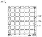
- FIG. 3illustrates a multi-cell, multilayer printed circuit board (PCB) panel used in the manufacturing of a stacking interposer, according to one aspect.
- PCBprinted circuit board
- FIG. 4illustrates the PCB panel of FIG. 3 slotted using a diamond saw process.
- FIG. 5illustrates cavities on the PCB panel of FIG. 4 after routing to clear out pillars.
- FIG. 6illustrates the inner side walls of the cavity and outer side walls of a cavity formed on the PCB panel of FIG. 5 .
- FIG. 7illustrates an example of drilling out the pillars prior to cutting the interposer walls.
- FIG. 8illustrates a method of manufacturing a stacking interposer, according to a first aspect.
- FIG. 9illustrates a method of manufacturing a stacking interposer, according to a second aspect.
- FIG. 10illustrates a method of manufacturing a memory module using a single reflow cycle, according to one aspect.
- a method for forming a stacking interposer that creates a compact and/or reliable interposer cavityinvolves a novel segmentation process that partially cuts a multi-cell, multi-layer PCB panel to a controlled depth along internal walls/edges of a cavity region within each of the interposer cell sites defined within the PCB panel. The material within the cavity region is then removed (by routing) to a controlled depth to form the internal cavity (i.e., bind cavity) for each of the interposer cell sites. The pillars may then be cut from the PCB panel.
- the corners of the cavitiesmay have a square configuration for fitting over the top of a BGA/memory device (which has very square corners). Consequently, the squaring of the cavity allows for a better fit over a BGA/memory device, which consequently leads to a more compact interposer size.
- the corners of the cavitiesmay be partially drilled to a controlled depth to remove pillars formed from the partial cuts of the PCB panel. Such removal of pillars forms an air gap from the outside to the inside cavity along the corners of the cavity at each interposer cell site.
- the interposermay then be used for stacking, for example, memory devices.
- the stacking interposermay create a vertical riser that makes electrical connections from an upper BGA device mounted on top of the stacking interposer to a base substrate (e.g., memory DIMM PCB).
- a base substratee.g., memory DIMM PCB
- an upper BGA/memory devicemay be mounted on the top side of the interposer while a lower BGA/memory device may be housed within the cavity of the interposer.
- the interposerdoes not necessarily join upper and lower memory devices electrically or mechanically.
- the interposermay be used to permit coupling memory devices onto a base substrate (e.g., memory DIMM PCB) using a single reflow process.
- a lower BGA/memory deviceis placed on the base substrate (e.g., memory DIMM PCB), and then the stacking interposer is placed over the lower BGA/memory device.
- the upper BGA/memory deviceis placed over the stacking interposer. The whole assembly is then reflowed to form the solder connections.
- FIG. 1illustrates a side perspective view of a package 100 having stacked Ball Grid Array (BGA) Dynamic random-access memory (DRAM) components on Joint Electron Devices Engineering Council (JEDEC) standard double data rate (DDR)2 and DDR3 dual in-line memory modules (DIMM), according to one aspect.
- the package 100may include a printed circuit board panel 102 having a plurality of stacking interposers 104 mounted to a first side of the printed circuit board panel 102 as well as a second opposing side of the printed circuit board panel 102 .
- Lower BGA DRAM devices(not shown) may be located under the plurality of stacking interposers 104 and upper lower BGA DRAM devices 106 may be located on top of the plurality of stacking interposers 104 .
- FIG. 2illustrates a cross-sectional view of a package utilizing a stacking interposer to mount an upper BGA chip over a lower BGA chip on a multilayer PCB panel, according to one aspect.
- the package 200may comprise a lower BGA DRAM device 202 directly coupled to a DIMM PCB 204 .
- a stacking interposer 206as described in further detail below, may be positioned over the lower BGA chip 202 , such as a BGA DRAM device, and the upper BGA chip 210 , such as upper BGA DRAM device, may be mounted to a top surface of the stacking interposer 206 .
- the stacking interposer 206may include a cavity 208 adapted to receive the lower BGA DRAM device 202 and form a gap 212 between the stacking interposer 206 and the lower BGA DRAM device 202 . If such gap 212 can be minimized, then the interposer 206 can be made smaller and more chips 202 can be fit within a given area. After placement (or coupling), the lower BGA DRAM device 202 , the stacking interposer 206 and the upper BGA DRAM device 210 may be simultaneously ultrasonically welded or soldered in place.
- the process of fabricating a stacking interposerstarts with a FR4 multilayer printed circuit board (PCB) panel manufactured using mainstream high speed multilayer PCB fabrication techniques.
- PCBprinted circuit board
- FIG. 3An example of a multi-cell, multilayer printed circuit board (PCB) panel 300 used in the manufacturing of a stacking interposer of the present disclosure is illustrated in FIG. 3
- the PCB panel 300may be comprised of a plurality of interposer cells 302 . Although thirty (30) interposer cells are shown (six (6) rows with five (5) interposer cells per row), this is by way of example only.
- the PCB panel 300may include more than or less than (6) rows and each row may include more than or less than (5) interposer cells.
- the PCB panel sizemay be approximately 4′′ ⁇ 3′′ with a thickness of 1.9 mm and a layer count of four (4).
- the next step in the processis to form controlled-depth cavities at each interposer cell site on the PCB panel 300 .
- One approach to forming a controlled-depth cavity in the PCB panel 300is to use a typical router bit process on a computer numerical control (CNC) mill as is known in the art.
- CNCcomputer numerical control
- a typical tolerance of a feature in a PCB cut with this router processis +/ ⁇ 0.005 in.
- the PCB panel 300is “slotted” using the diamond saw process.
- the saw bladeis used to cut the PCB panel 300 to a controlled depth (i.e. partial cut 304 ), stopping short of cutting all of the way through the PCB panel 300 leaving the PCB panel 300 intact.
- a saw cutis made for each inner wall only and the outer walls of the interposers are cut at a later stage.
- cell cavities of the slotted PCB panel 300 in FIG. 4are formed using typical PCB routing equipment.
- the router bitis used to clear out any remaining material left behind by the slotting process and is not needed to form the cavity walls.
- FIG. 5illustrates the square cavities 306 formed on the PCB panel 300 of FIG. 4 using the diamond saw process. If the inner corners of the cavity were formed with a standard router bit, the cavities would effectively be rounded (with approximate radius equal to the router bit radius). As a result, the overall cavity would be larger as the cavity must fit over the top of a BGA DRAM device (which has very square corners). Thus, using the diamond saw process enables a more area-efficient stacking interposer.
- FIG. 6illustrates the inner side walls 308 of a cavity and outer side walls 310 of the interposer formed on the PCB panel of FIG. 5 .
- the FR4 pillars 312 left behind as a result of the diamond saw processare removed. If the pillars 312 are not removed, the pillars 312 can break off potentially leaving debris in the DIMM assemblies. To prevent the pillars 312 breaking off and leaving debris behind, the pillars 312 are drilled out prior to the interposer walls being cut so that the no pillars are left behind.
- FIG. 7illustrates an example of drilling out the pillars 312 prior to cutting the interposer walls.
- FIG. 8illustrates a method of manufacturing a stacking interposer, according to one aspect.
- fabrication of a stacking interposermay begin with the formation of a multi-cell, multilayer PCB panel 802 .
- the panelmay be manufactured using mainstream high speed multilayer PCB fabrication techniques known in the art.
- the layer count, PCB thickness, dimensions, and the number of stacking interposer cells on the panelcan vary.
- controlled-depth cavitiesmay be formed at each interposer cell site on the panel using a diamond saw process, such as the diamond saw process used to singulate silicon chips from silicon wafers.
- a diamond saw processsuch as the diamond saw process used to singulate silicon chips from silicon wafers.
- the overall X-Y footprint of the BGA stackmay be minimized and tighter tolerances may be obtain, as compared to the typical tolerance of +/ ⁇ 0.005 inches in a PCB cut with the conventional router process.
- using the diamond saw processprovides for the inner corners of each cavity to have a notched out or square configuration.
- the inner side walls of each cell cavity of the stacking interposermay be formed. That is, the PCB panel may be “slotted” using the diamond saw process 804 (See FIG. 4 ). The saw blade may cut to a controlled depth (e.g., the depth of the cavity), short of cutting all of the way through the panel leaving the panel intact. The saw cut is made for each inner wall; the outer walls of the stacking interposers may be cut at a later stage in the process. Once the panel has been slotted, the slotted panel may then be placed on standard PCB routing equipment (e.g., router), where the cell cavities are formed 806 . (See FIG. 5 ) As the diamond saw process has previously formed the cavity inner walls, a router bit is not needed to form the cavity walls.
- standard PCB routing equipmente.g., router
- a router bitmay also be used to notch out the corners (at least to the depth of the cavity) 808 . (See FIG. 7 ) Clearing out the remaining material or “pillars” left behind by the slotting process avoids the possibility that the pillars can break off, potentially leaving debris in the DIMM assemblies. As such, the pillars may be drilled out prior to cutting the interposer walls so that no pillars are left behind. By removing the pillars, an air gap may be created allowing for air movement into and out of the cavity.
- having straight cornersmay be advantageous as the DRAM devices located within the cavity are typically square so the stacking interposer may be brought up to the edges of the DRAM device which in turn saves space on the board.
- the router bitis not needed to cut and define the inner side walls of the cavity. Consequently, as described above, a much more accurate, tighter tolerance cavity having notched out or square corners may be obtained. If the side walls of the cavity were cut with a router bit, the inner corners of the cavity may have a circular or rounded feature which would require the cavities to be bigger to fit over the DRAM devices.
- the panelmay be placed back on the diamond saw equipment and the outer interposer walls are cut, singulating the stacking interposer cells from the panel 810 .
- a stacking interposer for use in semiconductor packagingmay be prepared by the process comprising the steps of (a) forming a multi-cell, multilayer printed circuit board panel having a plurality of interposer cell sites; (b) slotting the panel using a diamond saw process to form inner walls of cell cavities; (c) forming a cavity at each interposer cell site on the panel using the diamond saw process, the inner corners of each cavity having a square configuration; (d) removing remaining material left behind by slotting process; and (e) cutting outer interposer walls using the diamond saw process.
- FIG. 9illustrates a method of manufacturing a stacking interposer, according to a second aspect.
- the order of the steps for fabricating the stacking interposermay be rearranged so that the diamond saw process is only used once.
- a multi-cell, multilayer PCB panelis formed 902 .
- the cavitiesmay be formed in the panel using a standard router process 904 as is known in the art.
- Using a diamond sawthe inner cavity side walls and the outer walls of the interposer cell sites are cut 906 . By cutting the inner cavity side walls and the outer walls of the interposer cell sites, the diamond saw equipment only needs to be set up once.
- a router bitmay then be used to form notched out corners in the interposer cell site by clearing out the remaining material, or “pillars”, 908 left behind by the cutting of the inner cavity walls and the outer walls of the interposer cell site.
- a stacking interposer for use in semiconductor packagingmay be prepared by the process comprising the steps of (a) forming a multi-cell, multilayer printed circuit board panel having a plurality of interposer cell sites; (b) forming a cavity at each interposer cell site on the panel using a router process; (c) cutting inner cavity walls and outer cavity walls of the each interposer cell site using a single diamond saw process; and (d) removing remaining material left behind when forming the cavity at the each interposer cell site.
- the DRAM devicesare exposed to two reflow cycles.
- the first reflow cycleis stack assembly formation and the second reflow cycle is stack attachment to the DIMM PCB.
- FIG. 10illustrates a method of manufacturing a ball grid array module using a single reflow cycle, according to one aspect.
- solder pastemay first be deposited down on a primary side of a base substrate (e.g., DIMM PCB) using, for example, a SMT solder paste stencil process 1002 .
- the solder pastemay be deposited on the pads for both a first (or lower) DRAM device and the stacking interposer in one solder paste deposition operation.
- the first (or lower) DRAM devicemay be placed on deposited solder paste using pick and place equipment 1004 .
- the stacking interposermay then be placed over the top of the first (or lower) DRAM device using the pick and place equipment 1006 .
- Solder balls of a second (or upper) DRAM devicemay be dipped in flux 1008 and then placed on the top of the stacking interposer using standard pick and place equipment.
- the DIMMmay then be reflowed to form the solder connections from the second (or upper) DRAM device to the interposer, from the interposer to the DIMM PCB, and from the first (or lower) DRAM device to the DIMM PCB 1012 .
- This same processmay be repeated for a second side of the DIMM PCB, completing assembly of the entire stacked DIMM.
- a ball grid array modulemay be prepared by the process comprising the steps of (a) depositing solder paste on a primary side of a dual in-line memory module (DIMM) printed circuit board using a surface mount technology solder paste stencil process; (b) placing a first dynamic random access memory device on the deposited solder paste; (c) placing a stacking interposer over the first dynamic random access memory device; (d) dipping solder balls of a second dynamic random access memory device in flux; (e) placing the dipped solder balls of the second first dynamic random access memory device on a top surface of the stacking interposer; and (f) performing a single reflow cycle to form solder connections between the second dynamic random access memory device and the interposer, between the interposer and the DIMM printed circuit board, and between the first dynamic random access memory device and the DIMM printed circuit board.
- DIMMdual in-line memory module
Landscapes
- Engineering & Computer Science (AREA)
- Microelectronics & Electronic Packaging (AREA)
- Power Engineering (AREA)
- Computer Hardware Design (AREA)
- Manufacturing & Machinery (AREA)
- Physics & Mathematics (AREA)
- Condensed Matter Physics & Semiconductors (AREA)
- General Physics & Mathematics (AREA)
- Mechanical Engineering (AREA)
- Ceramic Engineering (AREA)
- Semiconductor Memories (AREA)
Abstract
Description
Claims (16)
Priority Applications (2)
| Application Number | Priority Date | Filing Date | Title |
|---|---|---|---|
| US14/216,517US9016552B2 (en) | 2013-03-15 | 2014-03-17 | Method for forming interposers and stacked memory devices |
| US14/696,483US9287235B2 (en) | 2013-03-15 | 2015-04-27 | Method for forming interposers and stacked memory devices |
Applications Claiming Priority (2)
| Application Number | Priority Date | Filing Date | Title |
|---|---|---|---|
| US201361800801P | 2013-03-15 | 2013-03-15 | |
| US14/216,517US9016552B2 (en) | 2013-03-15 | 2014-03-17 | Method for forming interposers and stacked memory devices |
Related Child Applications (1)
| Application Number | Title | Priority Date | Filing Date |
|---|---|---|---|
| US14/696,483DivisionUS9287235B2 (en) | 2013-03-15 | 2015-04-27 | Method for forming interposers and stacked memory devices |
Publications (2)
| Publication Number | Publication Date |
|---|---|
| US20140263585A1 US20140263585A1 (en) | 2014-09-18 |
| US9016552B2true US9016552B2 (en) | 2015-04-28 |
Family
ID=51523112
Family Applications (2)
| Application Number | Title | Priority Date | Filing Date |
|---|---|---|---|
| US14/216,517ActiveUS9016552B2 (en) | 2013-03-15 | 2014-03-17 | Method for forming interposers and stacked memory devices |
| US14/696,483ActiveUS9287235B2 (en) | 2013-03-15 | 2015-04-27 | Method for forming interposers and stacked memory devices |
Family Applications After (1)
| Application Number | Title | Priority Date | Filing Date |
|---|---|---|---|
| US14/696,483ActiveUS9287235B2 (en) | 2013-03-15 | 2015-04-27 | Method for forming interposers and stacked memory devices |
Country Status (1)
| Country | Link |
|---|---|
| US (2) | US9016552B2 (en) |
Cited By (2)
| Publication number | Priority date | Publication date | Assignee | Title |
|---|---|---|---|---|
| US10497427B2 (en) | 2016-06-17 | 2019-12-03 | Samsung Electronics Co., Ltd. | Memory device using sense amplifiers as buffer memory with reduced access time and method of cache operation of the same |
| US10535395B2 (en) | 2016-06-20 | 2020-01-14 | Samsung Electronics Co., Ltd. | Memory device with improved latency and operating method thereof |
Families Citing this family (12)
| Publication number | Priority date | Publication date | Assignee | Title |
|---|---|---|---|---|
| GB201409650D0 (en)* | 2014-05-30 | 2014-07-16 | Bevan Heba | Manufacturing methods |
| SG11201704027PA (en)* | 2014-12-16 | 2017-06-29 | Intel Corp | Electronic assembly that includes stacked electronic devices |
| US9831579B1 (en) | 2016-08-01 | 2017-11-28 | Motorola Solutions, Inc. | Adapter frame with a set of electrical pads on its top and bottom surfaces for a board-to-board connection |
| KR102327548B1 (en) | 2017-10-17 | 2021-11-16 | 삼성전자주식회사 | Semiconductor device package |
| CN107908985B (en)* | 2017-10-24 | 2021-03-16 | 天津大学 | PCB board-level protection method and structure for ensuring integrated circuit chip communication |
| JP7153438B2 (en)* | 2017-10-26 | 2022-10-14 | 日東電工株式会社 | Substrate assembly sheet |
| US20190182955A1 (en)* | 2017-12-13 | 2019-06-13 | Intel Corporation | Replaceable on-package memory devices |
| KR102397905B1 (en) | 2017-12-27 | 2022-05-13 | 삼성전자주식회사 | Interposer substrate and semiconductor package |
| KR102653837B1 (en)* | 2018-07-27 | 2024-04-02 | 에스케이하이닉스 주식회사 | Memory module and data processing system |
| US20200367367A1 (en)* | 2019-05-15 | 2020-11-19 | Jabil Inc. | Method and Apparatus for Stacking Printed Circuit Board Assemblies with Single Reflow |
| EP4201163A4 (en)* | 2020-09-15 | 2024-03-20 | Jabil Inc. | Method and apparatus for stacking printed circuit board assemblies with single reflow |
| US11963296B2 (en) | 2021-10-07 | 2024-04-16 | Google Llc | Cavity printed circuit board for three-dimensional IC package |
Citations (44)
| Publication number | Priority date | Publication date | Assignee | Title |
|---|---|---|---|---|
| US5941447A (en)* | 1996-11-22 | 1999-08-24 | Ma Laboratories, Inc. | Manufacturing method for a processor module with dual-bank SRAM cache having shared capacitors |
| US6159757A (en)* | 1997-12-16 | 2000-12-12 | Sharp Kabushiki Kaisha | Process for producing a solar battery and a sheet material for protective covering thereof |
| US6213376B1 (en)* | 1998-06-17 | 2001-04-10 | International Business Machines Corp. | Stacked chip process carrier |
| US20020115235A1 (en)* | 2001-02-21 | 2002-08-22 | Hiroshi Sawada | Substrate cutting method |
| US20030016036A1 (en)* | 2001-07-19 | 2003-01-23 | Ahn Kie Y. | Full wafer silicon probe card for burn-in and testing, method of fabrication and test system including same |
| US20030045031A1 (en)* | 2001-08-28 | 2003-03-06 | Kazuo Kobayashi | Dicing method and dicing apparatus for dicing plate-like workpiece |
| US20030052098A1 (en)* | 2001-05-23 | 2003-03-20 | Gi-Heon Kim | Method and apparatus for cutting substrate using coolant |
| US20030232488A1 (en)* | 2002-06-14 | 2003-12-18 | Chua Swee Kwang | Wafer level packaging |
| US20040034993A1 (en)* | 2002-08-26 | 2004-02-26 | Matthew Rybka | Method for plasma etching to manufacture electrical devices having circuit protection |
| US20040113283A1 (en)* | 2002-03-06 | 2004-06-17 | Farnworth Warren M. | Method for fabricating encapsulated semiconductor components by etching |
| US6756251B2 (en)* | 2001-08-21 | 2004-06-29 | Micron Technology, Inc. | Method of manufacturing microelectronic devices, including methods of underfilling microelectronic components through an underfill aperture |
| US6782610B1 (en)* | 1999-05-21 | 2004-08-31 | North Corporation | Method for fabricating a wiring substrate by electroplating a wiring film on a metal base |
| US20040241962A1 (en)* | 2003-05-26 | 2004-12-02 | Yusuke Nagai | Method of dividing a non-metal substrate |
| US20050158968A1 (en)* | 2004-01-15 | 2005-07-21 | Disco Corporation | Wafer laser processing method |
| US20050167798A1 (en)* | 2004-01-29 | 2005-08-04 | Doan Trung T. | Die-wafer package and method of fabricating same |
| US20050170613A1 (en)* | 2004-02-03 | 2005-08-04 | Disco Corporation | Wafer dividing method |
| US20050269023A1 (en)* | 2004-06-07 | 2005-12-08 | Fujitsu Limited | Method of cutting laminate with laser and laminate |
| US20060043533A1 (en)* | 2004-08-24 | 2006-03-02 | Lake Rickie C | Wafer backside removal to complete through-holes and provide wafer singulation during the formation of a semiconductor device |
| US20060113286A1 (en)* | 2004-11-29 | 2006-06-01 | Fujitsu Limited | Stack structure cutting method and stack structure |
| US20060211220A1 (en)* | 2003-05-12 | 2006-09-21 | Tokyo Seimitsu Co., Ltd. | Method and device or dividing plate-like member |
| US20060289972A1 (en)* | 2005-06-28 | 2006-12-28 | Fujitsu Limited | Semiconductor device |
| US20070128834A1 (en)* | 2005-12-02 | 2007-06-07 | Disco Corporation | Wafer dividing method |
| US20070176181A1 (en)* | 2004-03-19 | 2007-08-02 | Katsuki Kusunoki | Compound semiconductor light-emitting device and production method thereof |
| US20080001699A1 (en)* | 2006-06-30 | 2008-01-03 | Gardner Donald S | Slotted magnetic material for integrated circuit inductors |
| US20080197484A1 (en)* | 2007-02-15 | 2008-08-21 | Headway Technologies, Inc. | Method of manufacturing electronic component package, and wafer and substructure used for manufacturing electronic component package |
| US20080299745A1 (en)* | 2007-05-30 | 2008-12-04 | Disco Corporation | Wafer separating method |
| US20090191693A1 (en)* | 2008-01-29 | 2009-07-30 | Disco Corporation | Wafer processing method |
| US20090203192A1 (en)* | 2008-02-13 | 2009-08-13 | Erdem Kaltalioglu | Crack Stop Trenches |
| US20090261480A1 (en)* | 2008-04-18 | 2009-10-22 | Alfred Martin | Integrated circuit and method of fabricating the same |
| US7820526B2 (en)* | 2005-05-20 | 2010-10-26 | Semiconductor Energy Laboratory Co., Ltd. | Manufacturing method of semiconductor device |
| US20100297855A1 (en)* | 2009-05-21 | 2010-11-25 | Disco Corporation | Device processing method |
| US20100304550A1 (en)* | 2009-05-26 | 2010-12-02 | Semiconductor Energy Laboratory Co., Ltd. | Manufacturing method of soi substrate |
| US20110124181A1 (en)* | 2009-11-20 | 2011-05-26 | Disco Corporation | Workpiece cutting method |
| US20110128713A1 (en)* | 2009-11-30 | 2011-06-02 | Renesas Electronics Corporation | Semiconductor device and method of manufacturing the same |
| US20120018194A1 (en)* | 2010-07-22 | 2012-01-26 | Ngk Spark Plug Co., Ltd. | Multilayer wiring board and manufacturing method thereof |
| US20120080673A1 (en)* | 2010-10-05 | 2012-04-05 | Sylvia Baumann Winter | Crack Stop Barrier and Method of Manufacturing Thereof |
| US8183091B2 (en)* | 1999-12-03 | 2012-05-22 | Renesas Electronics Corporation | Semiconductor integrated circuit device and process for manufacturing the same |
| US20120244682A1 (en)* | 2011-03-23 | 2012-09-27 | Disco Corporation | Wafer dividing method |
| US20120309169A1 (en)* | 2011-06-01 | 2012-12-06 | Disco Corporation | Laser processing method for wafer |
| US8485418B2 (en)* | 1995-05-26 | 2013-07-16 | Formfactor, Inc. | Method of wirebonding that utilizes a gas flow within a capillary from which a wire is played out |
| US20130230974A1 (en)* | 2011-03-14 | 2013-09-05 | Plasma-Therm Llc | Method and Apparatus for Plasma Dicing a Semi-conductor Wafer |
| US20140065767A1 (en)* | 2012-08-31 | 2014-03-06 | Renesas Electronics Corporation | Method of manufacturing semiconductor device |
| US20140206177A1 (en)* | 2013-01-23 | 2014-07-24 | Disco Corporation | Wafer processing method |
| US8883614B1 (en)* | 2013-05-22 | 2014-11-11 | Applied Materials, Inc. | Wafer dicing with wide kerf by laser scribing and plasma etching hybrid approach |
Family Cites Families (36)
| Publication number | Priority date | Publication date | Assignee | Title |
|---|---|---|---|---|
| US6117759A (en)* | 1997-01-03 | 2000-09-12 | Motorola Inc. | Method for multiplexed joining of solder bumps to various substrates during assembly of an integrated circuit package |
| US6225699B1 (en)* | 1998-06-26 | 2001-05-01 | International Business Machines Corporation | Chip-on-chip interconnections of varied characteristics |
| US6657134B2 (en)* | 2001-11-30 | 2003-12-02 | Honeywell International Inc. | Stacked ball grid array |
| US7205672B1 (en)* | 2001-12-05 | 2007-04-17 | National Semiconductor Corporation | Flip chip mounted to thermal sensing element through the back side of the chip |
| TWI237354B (en)* | 2002-01-31 | 2005-08-01 | Advanced Semiconductor Eng | Stacked package structure |
| JP2004253518A (en)* | 2003-02-19 | 2004-09-09 | Renesas Technology Corp | Semiconductor device and method of manufacturing same |
| CN1914001B (en)* | 2004-01-29 | 2010-09-01 | 松下电器产业株式会社 | Flux for soldering and soldering method |
| US7199466B2 (en)* | 2004-05-03 | 2007-04-03 | Intel Corporation | Package design using thermal linkage from die to printed circuit board |
| JP4827556B2 (en)* | 2005-03-18 | 2011-11-30 | キヤノン株式会社 | Stacked semiconductor package |
| WO2006106569A1 (en)* | 2005-03-31 | 2006-10-12 | Spansion Llc | Stacked type semiconductor device and method for manufacturing same |
| US7196427B2 (en)* | 2005-04-18 | 2007-03-27 | Freescale Semiconductor, Inc. | Structure having an integrated circuit on another integrated circuit with an intervening bent adhesive element |
| JP2007250764A (en)* | 2006-03-15 | 2007-09-27 | Elpida Memory Inc | Semiconductor device and manufacturing method therefor |
| US20080042265A1 (en)* | 2006-08-15 | 2008-02-21 | Merilo Leo A | Chip scale module package in bga semiconductor package |
| KR101332861B1 (en)* | 2007-01-03 | 2013-11-22 | 삼성전자주식회사 | IC package and manufacturing method |
| JP2009252893A (en)* | 2008-04-03 | 2009-10-29 | Elpida Memory Inc | Semiconductor device |
| US20090278262A1 (en)* | 2008-05-09 | 2009-11-12 | Boon Keat Tan | Multi-chip package including component supporting die overhang and system including same |
| US20090309236A1 (en)* | 2008-06-17 | 2009-12-17 | Mark Allen Gerber | Package on Package Structure with thin film Interposing Layer |
| US9893004B2 (en)* | 2011-07-27 | 2018-02-13 | Broadpak Corporation | Semiconductor interposer integration |
| TWI478257B (en)* | 2009-08-06 | 2015-03-21 | Htc Corp | Package structure and package process |
| US8884422B2 (en)* | 2009-12-31 | 2014-11-11 | Stmicroelectronics Pte Ltd. | Flip-chip fan-out wafer level package for package-on-package applications, and method of manufacture |
| US8502394B2 (en)* | 2009-12-31 | 2013-08-06 | Stmicroelectronics Pte Ltd. | Multi-stacked semiconductor dice scale package structure and method of manufacturing same |
| US9385095B2 (en)* | 2010-02-26 | 2016-07-05 | Taiwan Semiconductor Manufacturing Company, Ltd. | 3D semiconductor package interposer with die cavity |
| JP2011216818A (en)* | 2010-04-02 | 2011-10-27 | Elpida Memory Inc | Method of manufacturing semiconductor device |
| US8508045B2 (en)* | 2011-03-03 | 2013-08-13 | Broadcom Corporation | Package 3D interconnection and method of making same |
| US8873320B2 (en)* | 2011-08-17 | 2014-10-28 | Taiwan Semiconductor Manufacturing Co., Ltd. | DRAM repair architecture for wide I/O DRAM based 2.5D/3D system chips |
| US8946888B2 (en)* | 2011-09-30 | 2015-02-03 | Taiwan Semiconductor Manufacturing Company, Ltd. | Package on packaging structure and methods of making same |
| US8836136B2 (en)* | 2011-10-17 | 2014-09-16 | Invensas Corporation | Package-on-package assembly with wire bond vias |
| US8957518B2 (en)* | 2012-01-04 | 2015-02-17 | Mediatek Inc. | Molded interposer package and method for fabricating the same |
| US8372741B1 (en)* | 2012-02-24 | 2013-02-12 | Invensas Corporation | Method for package-on-package assembly with wire bonds to encapsulation surface |
| JP2013214578A (en)* | 2012-03-30 | 2013-10-17 | Ibiden Co Ltd | Wiring board and method for manufacturing the same |
| US9768105B2 (en)* | 2012-04-20 | 2017-09-19 | Taiwan Semiconductor Manufacturing Company, Ltd. | Rigid interconnect structures in package-on-package assemblies |
| US9385006B2 (en)* | 2012-06-21 | 2016-07-05 | STATS ChipPAC Pte. Ltd. | Semiconductor device and method of forming an embedded SOP fan-out package |
| US9087847B2 (en)* | 2012-08-14 | 2015-07-21 | Bridge Semiconductor Corporation | Thermally enhanced interconnect substrate with embedded semiconductor device and built-in stopper and method of making the same |
| US8963335B2 (en)* | 2012-09-13 | 2015-02-24 | Invensas Corporation | Tunable composite interposer |
| JP5543567B2 (en)* | 2012-10-22 | 2014-07-09 | 誠 雫石 | Manufacturing method of semiconductor device |
| US8796072B2 (en)* | 2012-11-15 | 2014-08-05 | Amkor Technology, Inc. | Method and system for a semiconductor device package with a die-to-die first bond |
- 2014
- 2014-03-17USUS14/216,517patent/US9016552B2/enactiveActive
- 2015
- 2015-04-27USUS14/696,483patent/US9287235B2/enactiveActive
Patent Citations (44)
| Publication number | Priority date | Publication date | Assignee | Title |
|---|---|---|---|---|
| US8485418B2 (en)* | 1995-05-26 | 2013-07-16 | Formfactor, Inc. | Method of wirebonding that utilizes a gas flow within a capillary from which a wire is played out |
| US5941447A (en)* | 1996-11-22 | 1999-08-24 | Ma Laboratories, Inc. | Manufacturing method for a processor module with dual-bank SRAM cache having shared capacitors |
| US6159757A (en)* | 1997-12-16 | 2000-12-12 | Sharp Kabushiki Kaisha | Process for producing a solar battery and a sheet material for protective covering thereof |
| US6213376B1 (en)* | 1998-06-17 | 2001-04-10 | International Business Machines Corp. | Stacked chip process carrier |
| US6782610B1 (en)* | 1999-05-21 | 2004-08-31 | North Corporation | Method for fabricating a wiring substrate by electroplating a wiring film on a metal base |
| US8183091B2 (en)* | 1999-12-03 | 2012-05-22 | Renesas Electronics Corporation | Semiconductor integrated circuit device and process for manufacturing the same |
| US20020115235A1 (en)* | 2001-02-21 | 2002-08-22 | Hiroshi Sawada | Substrate cutting method |
| US20030052098A1 (en)* | 2001-05-23 | 2003-03-20 | Gi-Heon Kim | Method and apparatus for cutting substrate using coolant |
| US20030016036A1 (en)* | 2001-07-19 | 2003-01-23 | Ahn Kie Y. | Full wafer silicon probe card for burn-in and testing, method of fabrication and test system including same |
| US6756251B2 (en)* | 2001-08-21 | 2004-06-29 | Micron Technology, Inc. | Method of manufacturing microelectronic devices, including methods of underfilling microelectronic components through an underfill aperture |
| US20030045031A1 (en)* | 2001-08-28 | 2003-03-06 | Kazuo Kobayashi | Dicing method and dicing apparatus for dicing plate-like workpiece |
| US20040113283A1 (en)* | 2002-03-06 | 2004-06-17 | Farnworth Warren M. | Method for fabricating encapsulated semiconductor components by etching |
| US20030232488A1 (en)* | 2002-06-14 | 2003-12-18 | Chua Swee Kwang | Wafer level packaging |
| US20040034993A1 (en)* | 2002-08-26 | 2004-02-26 | Matthew Rybka | Method for plasma etching to manufacture electrical devices having circuit protection |
| US20060211220A1 (en)* | 2003-05-12 | 2006-09-21 | Tokyo Seimitsu Co., Ltd. | Method and device or dividing plate-like member |
| US20040241962A1 (en)* | 2003-05-26 | 2004-12-02 | Yusuke Nagai | Method of dividing a non-metal substrate |
| US20050158968A1 (en)* | 2004-01-15 | 2005-07-21 | Disco Corporation | Wafer laser processing method |
| US20050167798A1 (en)* | 2004-01-29 | 2005-08-04 | Doan Trung T. | Die-wafer package and method of fabricating same |
| US20050170613A1 (en)* | 2004-02-03 | 2005-08-04 | Disco Corporation | Wafer dividing method |
| US20070176181A1 (en)* | 2004-03-19 | 2007-08-02 | Katsuki Kusunoki | Compound semiconductor light-emitting device and production method thereof |
| US20050269023A1 (en)* | 2004-06-07 | 2005-12-08 | Fujitsu Limited | Method of cutting laminate with laser and laminate |
| US20060043533A1 (en)* | 2004-08-24 | 2006-03-02 | Lake Rickie C | Wafer backside removal to complete through-holes and provide wafer singulation during the formation of a semiconductor device |
| US20060113286A1 (en)* | 2004-11-29 | 2006-06-01 | Fujitsu Limited | Stack structure cutting method and stack structure |
| US7820526B2 (en)* | 2005-05-20 | 2010-10-26 | Semiconductor Energy Laboratory Co., Ltd. | Manufacturing method of semiconductor device |
| US20060289972A1 (en)* | 2005-06-28 | 2006-12-28 | Fujitsu Limited | Semiconductor device |
| US20070128834A1 (en)* | 2005-12-02 | 2007-06-07 | Disco Corporation | Wafer dividing method |
| US20080001699A1 (en)* | 2006-06-30 | 2008-01-03 | Gardner Donald S | Slotted magnetic material for integrated circuit inductors |
| US20080197484A1 (en)* | 2007-02-15 | 2008-08-21 | Headway Technologies, Inc. | Method of manufacturing electronic component package, and wafer and substructure used for manufacturing electronic component package |
| US20080299745A1 (en)* | 2007-05-30 | 2008-12-04 | Disco Corporation | Wafer separating method |
| US20090191693A1 (en)* | 2008-01-29 | 2009-07-30 | Disco Corporation | Wafer processing method |
| US20090203192A1 (en)* | 2008-02-13 | 2009-08-13 | Erdem Kaltalioglu | Crack Stop Trenches |
| US20090261480A1 (en)* | 2008-04-18 | 2009-10-22 | Alfred Martin | Integrated circuit and method of fabricating the same |
| US20100297855A1 (en)* | 2009-05-21 | 2010-11-25 | Disco Corporation | Device processing method |
| US20100304550A1 (en)* | 2009-05-26 | 2010-12-02 | Semiconductor Energy Laboratory Co., Ltd. | Manufacturing method of soi substrate |
| US20110124181A1 (en)* | 2009-11-20 | 2011-05-26 | Disco Corporation | Workpiece cutting method |
| US20110128713A1 (en)* | 2009-11-30 | 2011-06-02 | Renesas Electronics Corporation | Semiconductor device and method of manufacturing the same |
| US20120018194A1 (en)* | 2010-07-22 | 2012-01-26 | Ngk Spark Plug Co., Ltd. | Multilayer wiring board and manufacturing method thereof |
| US20120080673A1 (en)* | 2010-10-05 | 2012-04-05 | Sylvia Baumann Winter | Crack Stop Barrier and Method of Manufacturing Thereof |
| US20130230974A1 (en)* | 2011-03-14 | 2013-09-05 | Plasma-Therm Llc | Method and Apparatus for Plasma Dicing a Semi-conductor Wafer |
| US20120244682A1 (en)* | 2011-03-23 | 2012-09-27 | Disco Corporation | Wafer dividing method |
| US20120309169A1 (en)* | 2011-06-01 | 2012-12-06 | Disco Corporation | Laser processing method for wafer |
| US20140065767A1 (en)* | 2012-08-31 | 2014-03-06 | Renesas Electronics Corporation | Method of manufacturing semiconductor device |
| US20140206177A1 (en)* | 2013-01-23 | 2014-07-24 | Disco Corporation | Wafer processing method |
| US8883614B1 (en)* | 2013-05-22 | 2014-11-11 | Applied Materials, Inc. | Wafer dicing with wide kerf by laser scribing and plasma etching hybrid approach |
Cited By (2)
| Publication number | Priority date | Publication date | Assignee | Title |
|---|---|---|---|---|
| US10497427B2 (en) | 2016-06-17 | 2019-12-03 | Samsung Electronics Co., Ltd. | Memory device using sense amplifiers as buffer memory with reduced access time and method of cache operation of the same |
| US10535395B2 (en) | 2016-06-20 | 2020-01-14 | Samsung Electronics Co., Ltd. | Memory device with improved latency and operating method thereof |
Also Published As
| Publication number | Publication date |
|---|---|
| US9287235B2 (en) | 2016-03-15 |
| US20140263585A1 (en) | 2014-09-18 |
| US20150228615A1 (en) | 2015-08-13 |
Similar Documents
| Publication | Publication Date | Title |
|---|---|---|
| US9287235B2 (en) | Method for forming interposers and stacked memory devices | |
| US9318465B2 (en) | Methods for forming a semiconductor device package | |
| US9502336B2 (en) | Coreless substrate with passive device pads | |
| US7145238B1 (en) | Semiconductor package and substrate having multi-level vias | |
| JP2007266572A (en) | Stack type semiconductor package | |
| US8476751B2 (en) | Stacked semiconductor package and method for manufacturing the same | |
| US10734317B2 (en) | Discrete electronic device embedded in chip module | |
| CN103904057A (en) | PoP structure and manufacturing technology | |
| KR102134933B1 (en) | Wiring substrate and wiring substrate fabrication method | |
| JP2004342861A (en) | Chip type electronic component, dummy wafer, methods of manufacturing them, and packaging structure of electronic component | |
| US20170040247A1 (en) | Substrate core with effective through substrate vias and method for making the same | |
| US6121678A (en) | Wrap-around interconnect for fine pitch ball grid array | |
| CN103687337A (en) | Laser machining method for package substrate through hole | |
| US10834817B2 (en) | Plated opening with vent path | |
| JP2011025399A (en) | Method for boring printed circuit board | |
| US20230089096A1 (en) | Multiple dies coupled with a glass core substrate | |
| TWI451824B (en) | Fabricating method for package carrier | |
| US20240055274A1 (en) | Semiconductor package carrier board structure and manufacturing method thereof | |
| US20240312888A1 (en) | Via structures in bonded glass substrates | |
| US20240312853A1 (en) | Via structures in bonded glass substrates | |
| TW201421642A (en) | Multi-substrate side-erecting package having 3D-carried passive components | |
| KR20140083580A (en) | Printed circuit board and method for manufacturing the same | |
| JP2007123545A (en) | Semiconductor device and manufacturing method thereof | |
| US9449890B1 (en) | Methods for temporary bussing of semiconductor package substrates | |
| JP2009124004A (en) | Electronic circuit module |
Legal Events
| Date | Code | Title | Description |
|---|---|---|---|
| AS | Assignment | Owner name:SANMINA CORPORATION, CALIFORNIA Free format text:ASSIGNMENT OF ASSIGNORS INTEREST;ASSIGNOR:SWEERE, PAUL;REEL/FRAME:035185/0778 Effective date:20150227 | |
| STCF | Information on status: patent grant | Free format text:PATENTED CASE | |
| AS | Assignment | Owner name:U.S. BANK NATIONAL ASSOCIATION, NOT IN ITS INDIVID Free format text:SECURITY INTEREST;ASSIGNOR:SANMINA CORPORATION;REEL/FRAME:036262/0978 Effective date:20150805 | |
| MAFP | Maintenance fee payment | Free format text:PAYMENT OF MAINTENANCE FEE, 4TH YEAR, LARGE ENTITY (ORIGINAL EVENT CODE: M1551); ENTITY STATUS OF PATENT OWNER: LARGE ENTITY Year of fee payment:4 | |
| AS | Assignment | Owner name:SCI TECHNOLOGY, CALIFORNIA Free format text:RELEASE BY SECURED PARTY;ASSIGNOR:U.S. BANK NATIONAL ASSOCIATION, SOLELY AS NOTES COLLATERAL AGENT;REEL/FRAME:049378/0927 Effective date:20190531 Owner name:HADCO CORPORATION, CALIFORNIA Free format text:RELEASE BY SECURED PARTY;ASSIGNOR:U.S. BANK NATIONAL ASSOCIATION, SOLELY AS NOTES COLLATERAL AGENT;REEL/FRAME:049378/0927 Effective date:20190531 Owner name:SANMINA CORPORATION, CALIFORNIA Free format text:RELEASE BY SECURED PARTY;ASSIGNOR:U.S. BANK NATIONAL ASSOCIATION, SOLELY AS NOTES COLLATERAL AGENT;REEL/FRAME:049378/0927 Effective date:20190531 Owner name:SENSORWISE, INC., CALIFORNIA Free format text:RELEASE BY SECURED PARTY;ASSIGNOR:U.S. BANK NATIONAL ASSOCIATION, SOLELY AS NOTES COLLATERAL AGENT;REEL/FRAME:049378/0927 Effective date:20190531 Owner name:HADCO SANTA CLARA, CALIFORNIA Free format text:RELEASE BY SECURED PARTY;ASSIGNOR:U.S. BANK NATIONAL ASSOCIATION, SOLELY AS NOTES COLLATERAL AGENT;REEL/FRAME:049378/0927 Effective date:20190531 | |
| MAFP | Maintenance fee payment | Free format text:PAYMENT OF MAINTENANCE FEE, 8TH YEAR, LARGE ENTITY (ORIGINAL EVENT CODE: M1552); ENTITY STATUS OF PATENT OWNER: LARGE ENTITY Year of fee payment:8 |