US9013029B2 - Joined body having an anti-corrosion film formed around a junction portion, and a semiconductor device having the same - Google Patents
Joined body having an anti-corrosion film formed around a junction portion, and a semiconductor device having the sameDownload PDFInfo
- Publication number
- US9013029B2 US9013029B2US13/882,436US201213882436AUS9013029B2US 9013029 B2US9013029 B2US 9013029B2US 201213882436 AUS201213882436 AUS 201213882436AUS 9013029 B2US9013029 B2US 9013029B2
- Authority
- US
- United States
- Prior art keywords
- junction
- target member
- metal plate
- metal
- joined body
- Prior art date
- Legal status (The legal status is an assumption and is not a legal conclusion. Google has not performed a legal analysis and makes no representation as to the accuracy of the status listed.)
- Active
Links
- 238000005260corrosionMethods0.000titleclaimsdescription20
- 239000004065semiconductorSubstances0.000titleclaimsdescription20
- 229910052751metalInorganic materials0.000claimsabstractdescription133
- 239000002184metalSubstances0.000claimsabstractdescription133
- 239000010949copperSubstances0.000claimsdescription22
- RYGMFSIKBFXOCR-UHFFFAOYSA-NCopperChemical compound[Cu]RYGMFSIKBFXOCR-UHFFFAOYSA-N0.000claimsdescription14
- 229910052802copperInorganic materials0.000claimsdescription14
- XEEYBQQBJWHFJM-UHFFFAOYSA-NIronChemical compound[Fe]XEEYBQQBJWHFJM-UHFFFAOYSA-N0.000claimsdescription7
- 239000000956alloySubstances0.000claimsdescription6
- 229910045601alloyInorganic materials0.000claimsdescription6
- BFSVOASYOCHEOV-UHFFFAOYSA-N2-diethylaminoethanolChemical compoundCCN(CC)CCOBFSVOASYOCHEOV-UHFFFAOYSA-N0.000claimsdescription3
- 238000006388chemical passivation reactionMethods0.000claims2
- 229910052742ironInorganic materials0.000claims2
- 239000007864aqueous solutionSubstances0.000abstractdescription41
- 238000005304joiningMethods0.000abstractdescription7
- 230000003647oxidationEffects0.000description20
- 238000007254oxidation reactionMethods0.000description20
- 238000000034methodMethods0.000description19
- 239000003112inhibitorSubstances0.000description15
- 150000002739metalsChemical class0.000description15
- PXHVJJICTQNCMI-UHFFFAOYSA-NNickelChemical compound[Ni]PXHVJJICTQNCMI-UHFFFAOYSA-N0.000description12
- 239000000243solutionSubstances0.000description12
- 238000007747platingMethods0.000description10
- 238000010438heat treatmentMethods0.000description9
- 238000004519manufacturing processMethods0.000description8
- 239000003795chemical substances by applicationSubstances0.000description7
- 238000000518rheometryMethods0.000description7
- HEMHJVSKTPXQMS-UHFFFAOYSA-MSodium hydroxideChemical compound[OH-].[Na+]HEMHJVSKTPXQMS-UHFFFAOYSA-M0.000description6
- WABPQHHGFIMREM-VENIDDJXSA-Nlead-201Chemical compound[201Pb]WABPQHHGFIMREM-VENIDDJXSA-N0.000description6
- WABPQHHGFIMREM-FTXFMUIASA-Nlead-202Chemical compound[202Pb]WABPQHHGFIMREM-FTXFMUIASA-N0.000description6
- 239000000463materialSubstances0.000description6
- QTBSBXVTEAMEQO-UHFFFAOYSA-NAcetic acidChemical compoundCC(O)=OQTBSBXVTEAMEQO-UHFFFAOYSA-N0.000description5
- WMFOQBRAJBCJND-UHFFFAOYSA-MLithium hydroxideChemical compound[Li+].[OH-]WMFOQBRAJBCJND-UHFFFAOYSA-M0.000description5
- 229910052759nickelInorganic materials0.000description5
- 230000036961partial effectEffects0.000description5
- KWYUFKZDYYNOTN-UHFFFAOYSA-MPotassium hydroxideChemical group[OH-].[K+]KWYUFKZDYYNOTN-UHFFFAOYSA-M0.000description4
- JEIPFZHSYJVQDO-UHFFFAOYSA-Niron(III) oxideInorganic materialsO=[Fe]O[Fe]=OJEIPFZHSYJVQDO-UHFFFAOYSA-N0.000description4
- 230000007774longtermEffects0.000description4
- 238000003825pressingMethods0.000description4
- 239000004411aluminiumSubstances0.000description3
- 229910052782aluminiumInorganic materials0.000description3
- XAGFODPZIPBFFR-UHFFFAOYSA-NaluminiumChemical compound[Al]XAGFODPZIPBFFR-UHFFFAOYSA-N0.000description3
- 238000005219brazingMethods0.000description3
- 230000007797corrosionEffects0.000description3
- 230000002401inhibitory effectEffects0.000description3
- BDAGIHXWWSANSR-UHFFFAOYSA-Nmethanoic acidNatural productsOC=OBDAGIHXWWSANSR-UHFFFAOYSA-N0.000description3
- 230000002093peripheral effectEffects0.000description3
- 229920001451polypropylene glycolPolymers0.000description3
- 230000002265preventionEffects0.000description3
- 238000003466weldingMethods0.000description3
- 239000002202Polyethylene glycolSubstances0.000description2
- BQCADISMDOOEFD-UHFFFAOYSA-NSilverChemical compound[Ag]BQCADISMDOOEFD-UHFFFAOYSA-N0.000description2
- 230000008901benefitEffects0.000description2
- 238000007796conventional methodMethods0.000description2
- 235000019253formic acidNutrition0.000description2
- 239000010931goldSubstances0.000description2
- 229920001223polyethylene glycolPolymers0.000description2
- 238000001878scanning electron micrographMethods0.000description2
- 229910052709silverInorganic materials0.000description2
- 239000004332silverSubstances0.000description2
- OSWFIVFLDKOXQC-UHFFFAOYSA-N4-(3-methoxyphenyl)anilineChemical compoundCOC1=CC=CC(C=2C=CC(N)=CC=2)=C1OSWFIVFLDKOXQC-UHFFFAOYSA-N0.000description1
- XBPCUCUWBYBCDP-UHFFFAOYSA-NDicyclohexylamineChemical compoundC1CCCCC1NC1CCCCC1XBPCUCUWBYBCDP-UHFFFAOYSA-N0.000description1
- OAICVXFJPJFONN-UHFFFAOYSA-NPhosphorusChemical compound[P]OAICVXFJPJFONN-UHFFFAOYSA-N0.000description1
- XUIMIQQOPSSXEZ-UHFFFAOYSA-NSiliconChemical compound[Si]XUIMIQQOPSSXEZ-UHFFFAOYSA-N0.000description1
- ATJFFYVFTNAWJD-UHFFFAOYSA-NTinChemical compound[Sn]ATJFFYVFTNAWJD-UHFFFAOYSA-N0.000description1
- 239000002253acidSubstances0.000description1
- 230000002411adverseEffects0.000description1
- QVGXLLKOCUKJST-UHFFFAOYSA-Natomic oxygenChemical compound[O]QVGXLLKOCUKJST-UHFFFAOYSA-N0.000description1
- 230000015572biosynthetic processEffects0.000description1
- 230000006866deteriorationEffects0.000description1
- ZBCBWPMODOFKDW-UHFFFAOYSA-NdiethanolamineChemical compoundOCCNCCOZBCBWPMODOFKDW-UHFFFAOYSA-N0.000description1
- 238000005530etchingMethods0.000description1
- 230000008020evaporationEffects0.000description1
- 238000001704evaporationMethods0.000description1
- 230000005669field effectEffects0.000description1
- PCHJSUWPFVWCPO-UHFFFAOYSA-NgoldChemical compound[Au]PCHJSUWPFVWCPO-UHFFFAOYSA-N0.000description1
- 229910052737goldInorganic materials0.000description1
- 239000011810insulating materialSubstances0.000description1
- 229910044991metal oxideInorganic materials0.000description1
- 150000004706metal oxidesChemical class0.000description1
- 238000004021metal weldingMethods0.000description1
- 238000001000micrographMethods0.000description1
- 239000000203mixtureSubstances0.000description1
- 230000001590oxidative effectEffects0.000description1
- 229910052760oxygenInorganic materials0.000description1
- 239000001301oxygenSubstances0.000description1
- 239000002245particleSubstances0.000description1
- 239000011574phosphorusSubstances0.000description1
- 229910052698phosphorusInorganic materials0.000description1
- 239000004033plasticSubstances0.000description1
- 229920003023plasticPolymers0.000description1
- 230000003449preventive effectEffects0.000description1
- 230000002829reductive effectEffects0.000description1
- 239000011347resinSubstances0.000description1
- 229920005989resinPolymers0.000description1
- VSZWPYCFIRKVQL-UHFFFAOYSA-Nselanylidenegallium;seleniumChemical compound[Se].[Se]=[Ga].[Se]=[Ga]VSZWPYCFIRKVQL-UHFFFAOYSA-N0.000description1
- 229910052710siliconInorganic materials0.000description1
- 239000010703siliconSubstances0.000description1
- 229910000679solderInorganic materials0.000description1
- 238000003756stirringMethods0.000description1
- XLYOFNOQVPJJNP-UHFFFAOYSA-NwaterSubstancesOXLYOFNOQVPJJNP-UHFFFAOYSA-N0.000description1
Images


Classifications
- H—ELECTRICITY
- H01—ELECTRIC ELEMENTS
- H01L—SEMICONDUCTOR DEVICES NOT COVERED BY CLASS H10
- H01L21/00—Processes or apparatus adapted for the manufacture or treatment of semiconductor or solid state devices or of parts thereof
- H01L21/02—Manufacture or treatment of semiconductor devices or of parts thereof
- H01L21/04—Manufacture or treatment of semiconductor devices or of parts thereof the devices having potential barriers, e.g. a PN junction, depletion layer or carrier concentration layer
- H01L21/48—Manufacture or treatment of parts, e.g. containers, prior to assembly of the devices, using processes not provided for in a single one of the groups H01L21/18 - H01L21/326 or H10D48/04 - H10D48/07
- H01L21/4814—Conductive parts
- H01L21/4821—Flat leads, e.g. lead frames with or without insulating supports
- H01L21/4842—Mechanical treatment, e.g. punching, cutting, deforming, cold welding
- H—ELECTRICITY
- H01—ELECTRIC ELEMENTS
- H01L—SEMICONDUCTOR DEVICES NOT COVERED BY CLASS H10
- H01L23/00—Details of semiconductor or other solid state devices
- H01L23/34—Arrangements for cooling, heating, ventilating or temperature compensation ; Temperature sensing arrangements
- H01L23/42—Fillings or auxiliary members in containers or encapsulations selected or arranged to facilitate heating or cooling
- H01L23/433—Auxiliary members in containers characterised by their shape, e.g. pistons
- H01L23/4334—Auxiliary members in encapsulations
- B—PERFORMING OPERATIONS; TRANSPORTING
- B23—MACHINE TOOLS; METAL-WORKING NOT OTHERWISE PROVIDED FOR
- B23K—SOLDERING OR UNSOLDERING; WELDING; CLADDING OR PLATING BY SOLDERING OR WELDING; CUTTING BY APPLYING HEAT LOCALLY, e.g. FLAME CUTTING; WORKING BY LASER BEAM
- B23K20/00—Non-electric welding by applying impact or other pressure, with or without the application of heat, e.g. cladding or plating
- B23K20/02—Non-electric welding by applying impact or other pressure, with or without the application of heat, e.g. cladding or plating by means of a press ; Diffusion bonding
- B23K20/023—Thermo-compression bonding
- B—PERFORMING OPERATIONS; TRANSPORTING
- B23—MACHINE TOOLS; METAL-WORKING NOT OTHERWISE PROVIDED FOR
- B23K—SOLDERING OR UNSOLDERING; WELDING; CLADDING OR PLATING BY SOLDERING OR WELDING; CUTTING BY APPLYING HEAT LOCALLY, e.g. FLAME CUTTING; WORKING BY LASER BEAM
- B23K20/00—Non-electric welding by applying impact or other pressure, with or without the application of heat, e.g. cladding or plating
- B23K20/16—Non-electric welding by applying impact or other pressure, with or without the application of heat, e.g. cladding or plating with interposition of special material to facilitate connection of the parts, e.g. material for absorbing or producing gas
- B—PERFORMING OPERATIONS; TRANSPORTING
- B23—MACHINE TOOLS; METAL-WORKING NOT OTHERWISE PROVIDED FOR
- B23K—SOLDERING OR UNSOLDERING; WELDING; CLADDING OR PLATING BY SOLDERING OR WELDING; CUTTING BY APPLYING HEAT LOCALLY, e.g. FLAME CUTTING; WORKING BY LASER BEAM
- B23K20/00—Non-electric welding by applying impact or other pressure, with or without the application of heat, e.g. cladding or plating
- B23K20/22—Non-electric welding by applying impact or other pressure, with or without the application of heat, e.g. cladding or plating taking account of the properties of the materials to be welded
- B23K20/227—Non-electric welding by applying impact or other pressure, with or without the application of heat, e.g. cladding or plating taking account of the properties of the materials to be welded with ferrous layer
- B—PERFORMING OPERATIONS; TRANSPORTING
- B23—MACHINE TOOLS; METAL-WORKING NOT OTHERWISE PROVIDED FOR
- B23K—SOLDERING OR UNSOLDERING; WELDING; CLADDING OR PLATING BY SOLDERING OR WELDING; CUTTING BY APPLYING HEAT LOCALLY, e.g. FLAME CUTTING; WORKING BY LASER BEAM
- B23K20/00—Non-electric welding by applying impact or other pressure, with or without the application of heat, e.g. cladding or plating
- B23K20/22—Non-electric welding by applying impact or other pressure, with or without the application of heat, e.g. cladding or plating taking account of the properties of the materials to be welded
- B23K20/233—Non-electric welding by applying impact or other pressure, with or without the application of heat, e.g. cladding or plating taking account of the properties of the materials to be welded without ferrous layer
- B—PERFORMING OPERATIONS; TRANSPORTING
- B23—MACHINE TOOLS; METAL-WORKING NOT OTHERWISE PROVIDED FOR
- B23K—SOLDERING OR UNSOLDERING; WELDING; CLADDING OR PLATING BY SOLDERING OR WELDING; CUTTING BY APPLYING HEAT LOCALLY, e.g. FLAME CUTTING; WORKING BY LASER BEAM
- B23K35/00—Rods, electrodes, materials, or media, for use in soldering, welding, or cutting
- B23K35/001—Interlayers, transition pieces for metallurgical bonding of workpieces
- B23K35/002—Interlayers, transition pieces for metallurgical bonding of workpieces at least one of the workpieces being of light metal
- B—PERFORMING OPERATIONS; TRANSPORTING
- B23—MACHINE TOOLS; METAL-WORKING NOT OTHERWISE PROVIDED FOR
- B23K—SOLDERING OR UNSOLDERING; WELDING; CLADDING OR PLATING BY SOLDERING OR WELDING; CUTTING BY APPLYING HEAT LOCALLY, e.g. FLAME CUTTING; WORKING BY LASER BEAM
- B23K35/00—Rods, electrodes, materials, or media, for use in soldering, welding, or cutting
- B23K35/001—Interlayers, transition pieces for metallurgical bonding of workpieces
- B23K35/004—Interlayers, transition pieces for metallurgical bonding of workpieces at least one of the workpieces being of a metal of the iron group
- B—PERFORMING OPERATIONS; TRANSPORTING
- B23—MACHINE TOOLS; METAL-WORKING NOT OTHERWISE PROVIDED FOR
- B23K—SOLDERING OR UNSOLDERING; WELDING; CLADDING OR PLATING BY SOLDERING OR WELDING; CUTTING BY APPLYING HEAT LOCALLY, e.g. FLAME CUTTING; WORKING BY LASER BEAM
- B23K35/00—Rods, electrodes, materials, or media, for use in soldering, welding, or cutting
- B23K35/001—Interlayers, transition pieces for metallurgical bonding of workpieces
- B23K35/007—Interlayers, transition pieces for metallurgical bonding of workpieces at least one of the workpieces being of copper or another noble metal
- H—ELECTRICITY
- H01—ELECTRIC ELEMENTS
- H01L—SEMICONDUCTOR DEVICES NOT COVERED BY CLASS H10
- H01L21/00—Processes or apparatus adapted for the manufacture or treatment of semiconductor or solid state devices or of parts thereof
- H01L21/02—Manufacture or treatment of semiconductor devices or of parts thereof
- H01L21/04—Manufacture or treatment of semiconductor devices or of parts thereof the devices having potential barriers, e.g. a PN junction, depletion layer or carrier concentration layer
- H01L21/48—Manufacture or treatment of parts, e.g. containers, prior to assembly of the devices, using processes not provided for in a single one of the groups H01L21/18 - H01L21/326 or H10D48/04 - H10D48/07
- H01L21/4814—Conductive parts
- H01L21/4821—Flat leads, e.g. lead frames with or without insulating supports
- H01L21/4825—Connection or disconnection of other leads to or from flat leads, e.g. wires, bumps, other flat leads
- H—ELECTRICITY
- H01—ELECTRIC ELEMENTS
- H01L—SEMICONDUCTOR DEVICES NOT COVERED BY CLASS H10
- H01L21/00—Processes or apparatus adapted for the manufacture or treatment of semiconductor or solid state devices or of parts thereof
- H01L21/02—Manufacture or treatment of semiconductor devices or of parts thereof
- H01L21/04—Manufacture or treatment of semiconductor devices or of parts thereof the devices having potential barriers, e.g. a PN junction, depletion layer or carrier concentration layer
- H01L21/48—Manufacture or treatment of parts, e.g. containers, prior to assembly of the devices, using processes not provided for in a single one of the groups H01L21/18 - H01L21/326 or H10D48/04 - H10D48/07
- H01L21/4814—Conductive parts
- H01L21/4821—Flat leads, e.g. lead frames with or without insulating supports
- H01L21/4835—Cleaning, e.g. removing of solder
- H—ELECTRICITY
- H01—ELECTRIC ELEMENTS
- H01L—SEMICONDUCTOR DEVICES NOT COVERED BY CLASS H10
- H01L23/00—Details of semiconductor or other solid state devices
- H01L23/48—Arrangements for conducting electric current to or from the solid state body in operation, e.g. leads, terminal arrangements ; Selection of materials therefor
- H01L23/488—Arrangements for conducting electric current to or from the solid state body in operation, e.g. leads, terminal arrangements ; Selection of materials therefor consisting of soldered or bonded constructions
- H01L23/495—Lead-frames or other flat leads
- H01L23/49537—Plurality of lead frames mounted in one device
- H—ELECTRICITY
- H01—ELECTRIC ELEMENTS
- H01L—SEMICONDUCTOR DEVICES NOT COVERED BY CLASS H10
- H01L23/00—Details of semiconductor or other solid state devices
- H01L23/48—Arrangements for conducting electric current to or from the solid state body in operation, e.g. leads, terminal arrangements ; Selection of materials therefor
- H01L23/488—Arrangements for conducting electric current to or from the solid state body in operation, e.g. leads, terminal arrangements ; Selection of materials therefor consisting of soldered or bonded constructions
- H01L23/495—Lead-frames or other flat leads
- H01L23/49575—Assemblies of semiconductor devices on lead frames
- B—PERFORMING OPERATIONS; TRANSPORTING
- B23—MACHINE TOOLS; METAL-WORKING NOT OTHERWISE PROVIDED FOR
- B23K—SOLDERING OR UNSOLDERING; WELDING; CLADDING OR PLATING BY SOLDERING OR WELDING; CUTTING BY APPLYING HEAT LOCALLY, e.g. FLAME CUTTING; WORKING BY LASER BEAM
- B23K2101/00—Articles made by soldering, welding or cutting
- B23K2101/18—Sheet panels
- B—PERFORMING OPERATIONS; TRANSPORTING
- B23—MACHINE TOOLS; METAL-WORKING NOT OTHERWISE PROVIDED FOR
- B23K—SOLDERING OR UNSOLDERING; WELDING; CLADDING OR PLATING BY SOLDERING OR WELDING; CUTTING BY APPLYING HEAT LOCALLY, e.g. FLAME CUTTING; WORKING BY LASER BEAM
- B23K2101/00—Articles made by soldering, welding or cutting
- B23K2101/36—Electric or electronic devices
- B23K2101/42—Printed circuits
- B—PERFORMING OPERATIONS; TRANSPORTING
- B23—MACHINE TOOLS; METAL-WORKING NOT OTHERWISE PROVIDED FOR
- B23K—SOLDERING OR UNSOLDERING; WELDING; CLADDING OR PLATING BY SOLDERING OR WELDING; CUTTING BY APPLYING HEAT LOCALLY, e.g. FLAME CUTTING; WORKING BY LASER BEAM
- B23K2103/00—Materials to be soldered, welded or cut
- B23K2103/02—Iron or ferrous alloys
- B23K2103/04—Steel or steel alloys
- B—PERFORMING OPERATIONS; TRANSPORTING
- B23—MACHINE TOOLS; METAL-WORKING NOT OTHERWISE PROVIDED FOR
- B23K—SOLDERING OR UNSOLDERING; WELDING; CLADDING OR PLATING BY SOLDERING OR WELDING; CUTTING BY APPLYING HEAT LOCALLY, e.g. FLAME CUTTING; WORKING BY LASER BEAM
- B23K2103/00—Materials to be soldered, welded or cut
- B23K2103/08—Non-ferrous metals or alloys
- B23K2103/10—Aluminium or alloys thereof
- B—PERFORMING OPERATIONS; TRANSPORTING
- B23—MACHINE TOOLS; METAL-WORKING NOT OTHERWISE PROVIDED FOR
- B23K—SOLDERING OR UNSOLDERING; WELDING; CLADDING OR PLATING BY SOLDERING OR WELDING; CUTTING BY APPLYING HEAT LOCALLY, e.g. FLAME CUTTING; WORKING BY LASER BEAM
- B23K2103/00—Materials to be soldered, welded or cut
- B23K2103/08—Non-ferrous metals or alloys
- B23K2103/12—Copper or alloys thereof
- B23K2201/18—
- B23K2201/42—
- B23K2203/04—
- B23K2203/10—
- B23K2203/12—
- H—ELECTRICITY
- H01—ELECTRIC ELEMENTS
- H01L—SEMICONDUCTOR DEVICES NOT COVERED BY CLASS H10
- H01L2224/00—Indexing scheme for arrangements for connecting or disconnecting semiconductor or solid-state bodies and methods related thereto as covered by H01L24/00
- H01L2224/01—Means for bonding being attached to, or being formed on, the surface to be connected, e.g. chip-to-package, die-attach, "first-level" interconnects; Manufacturing methods related thereto
- H01L2224/26—Layer connectors, e.g. plate connectors, solder or adhesive layers; Manufacturing methods related thereto
- H01L2224/31—Structure, shape, material or disposition of the layer connectors after the connecting process
- H01L2224/32—Structure, shape, material or disposition of the layer connectors after the connecting process of an individual layer connector
- H01L2224/321—Disposition
- H01L2224/32151—Disposition the layer connector connecting between a semiconductor or solid-state body and an item not being a semiconductor or solid-state body, e.g. chip-to-substrate, chip-to-passive
- H01L2224/32221—Disposition the layer connector connecting between a semiconductor or solid-state body and an item not being a semiconductor or solid-state body, e.g. chip-to-substrate, chip-to-passive the body and the item being stacked
- H01L2224/32245—Disposition the layer connector connecting between a semiconductor or solid-state body and an item not being a semiconductor or solid-state body, e.g. chip-to-substrate, chip-to-passive the body and the item being stacked the item being metallic
- H—ELECTRICITY
- H01—ELECTRIC ELEMENTS
- H01L—SEMICONDUCTOR DEVICES NOT COVERED BY CLASS H10
- H01L2224/00—Indexing scheme for arrangements for connecting or disconnecting semiconductor or solid-state bodies and methods related thereto as covered by H01L24/00
- H01L2224/01—Means for bonding being attached to, or being formed on, the surface to be connected, e.g. chip-to-package, die-attach, "first-level" interconnects; Manufacturing methods related thereto
- H01L2224/42—Wire connectors; Manufacturing methods related thereto
- H01L2224/47—Structure, shape, material or disposition of the wire connectors after the connecting process
- H01L2224/48—Structure, shape, material or disposition of the wire connectors after the connecting process of an individual wire connector
- H01L2224/4805—Shape
- H01L2224/4809—Loop shape
- H01L2224/48091—Arched
- H—ELECTRICITY
- H01—ELECTRIC ELEMENTS
- H01L—SEMICONDUCTOR DEVICES NOT COVERED BY CLASS H10
- H01L2224/00—Indexing scheme for arrangements for connecting or disconnecting semiconductor or solid-state bodies and methods related thereto as covered by H01L24/00
- H01L2224/01—Means for bonding being attached to, or being formed on, the surface to be connected, e.g. chip-to-package, die-attach, "first-level" interconnects; Manufacturing methods related thereto
- H01L2224/42—Wire connectors; Manufacturing methods related thereto
- H01L2224/47—Structure, shape, material or disposition of the wire connectors after the connecting process
- H01L2224/48—Structure, shape, material or disposition of the wire connectors after the connecting process of an individual wire connector
- H01L2224/481—Disposition
- H01L2224/48151—Connecting between a semiconductor or solid-state body and an item not being a semiconductor or solid-state body, e.g. chip-to-substrate, chip-to-passive
- H01L2224/48221—Connecting between a semiconductor or solid-state body and an item not being a semiconductor or solid-state body, e.g. chip-to-substrate, chip-to-passive the body and the item being stacked
- H01L2224/48245—Connecting between a semiconductor or solid-state body and an item not being a semiconductor or solid-state body, e.g. chip-to-substrate, chip-to-passive the body and the item being stacked the item being metallic
- H01L2224/48247—Connecting between a semiconductor or solid-state body and an item not being a semiconductor or solid-state body, e.g. chip-to-substrate, chip-to-passive the body and the item being stacked the item being metallic connecting the wire to a bond pad of the item
- H—ELECTRICITY
- H01—ELECTRIC ELEMENTS
- H01L—SEMICONDUCTOR DEVICES NOT COVERED BY CLASS H10
- H01L2224/00—Indexing scheme for arrangements for connecting or disconnecting semiconductor or solid-state bodies and methods related thereto as covered by H01L24/00
- H01L2224/73—Means for bonding being of different types provided for in two or more of groups H01L2224/10, H01L2224/18, H01L2224/26, H01L2224/34, H01L2224/42, H01L2224/50, H01L2224/63, H01L2224/71
- H01L2224/732—Location after the connecting process
- H01L2224/73251—Location after the connecting process on different surfaces
- H01L2224/73265—Layer and wire connectors
- H—ELECTRICITY
- H01—ELECTRIC ELEMENTS
- H01L—SEMICONDUCTOR DEVICES NOT COVERED BY CLASS H10
- H01L24/00—Arrangements for connecting or disconnecting semiconductor or solid-state bodies; Methods or apparatus related thereto
- H01L24/73—Means for bonding being of different types provided for in two or more of groups H01L24/10, H01L24/18, H01L24/26, H01L24/34, H01L24/42, H01L24/50, H01L24/63, H01L24/71
- H—ELECTRICITY
- H01—ELECTRIC ELEMENTS
- H01L—SEMICONDUCTOR DEVICES NOT COVERED BY CLASS H10
- H01L2924/00—Indexing scheme for arrangements or methods for connecting or disconnecting semiconductor or solid-state bodies as covered by H01L24/00
- H—ELECTRICITY
- H01—ELECTRIC ELEMENTS
- H01L—SEMICONDUCTOR DEVICES NOT COVERED BY CLASS H10
- H01L2924/00—Indexing scheme for arrangements or methods for connecting or disconnecting semiconductor or solid-state bodies as covered by H01L24/00
- H01L2924/0001—Technical content checked by a classifier
- H01L2924/00012—Relevant to the scope of the group, the symbol of which is combined with the symbol of this group
- H—ELECTRICITY
- H01—ELECTRIC ELEMENTS
- H01L—SEMICONDUCTOR DEVICES NOT COVERED BY CLASS H10
- H01L2924/00—Indexing scheme for arrangements or methods for connecting or disconnecting semiconductor or solid-state bodies as covered by H01L24/00
- H01L2924/0001—Technical content checked by a classifier
- H01L2924/00014—Technical content checked by a classifier the subject-matter covered by the group, the symbol of which is combined with the symbol of this group, being disclosed without further technical details
- H—ELECTRICITY
- H01—ELECTRIC ELEMENTS
- H01L—SEMICONDUCTOR DEVICES NOT COVERED BY CLASS H10
- H01L2924/00—Indexing scheme for arrangements or methods for connecting or disconnecting semiconductor or solid-state bodies as covered by H01L24/00
- H01L2924/10—Details of semiconductor or other solid state devices to be connected
- H01L2924/11—Device type
- H01L2924/13—Discrete devices, e.g. 3 terminal devices
- H01L2924/1304—Transistor
- H01L2924/1305—Bipolar Junction Transistor [BJT]
- H01L2924/13055—Insulated gate bipolar transistor [IGBT]
- H—ELECTRICITY
- H01—ELECTRIC ELEMENTS
- H01L—SEMICONDUCTOR DEVICES NOT COVERED BY CLASS H10
- H01L2924/00—Indexing scheme for arrangements or methods for connecting or disconnecting semiconductor or solid-state bodies as covered by H01L24/00
- H01L2924/10—Details of semiconductor or other solid state devices to be connected
- H01L2924/11—Device type
- H01L2924/13—Discrete devices, e.g. 3 terminal devices
- H01L2924/1304—Transistor
- H01L2924/1306—Field-effect transistor [FET]
- H01L2924/13091—Metal-Oxide-Semiconductor Field-Effect Transistor [MOSFET]
- H—ELECTRICITY
- H01—ELECTRIC ELEMENTS
- H01L—SEMICONDUCTOR DEVICES NOT COVERED BY CLASS H10
- H01L2924/00—Indexing scheme for arrangements or methods for connecting or disconnecting semiconductor or solid-state bodies as covered by H01L24/00
- H01L2924/15—Details of package parts other than the semiconductor or other solid state devices to be connected
- H01L2924/181—Encapsulation
Definitions
- the present disclosurerelates to techniques of joining junction target members together, and more particularly to a joined body, a power semiconductor device, and manufacturing methods of joined body and the power semiconductor device.
- junction target membersmembers to be joined
- a plate member 2 a whose front and back surfaces are coated with plating layers 8 a and a plate member 2 b whose front and back surfaces are coated with plating layers 8 bare stacked.
- the plating layers 8 a and 8 bare made of nickel (Ni), and the plate members 2 a and 2 b are made of copper (Cu).
- each contact surface of a dice 6 ais brought into contact with the plate member 2 a with the plating layer 8 a interposed therebetween, and a pressure is applied to the plate member 2 a in the direction indicated by the arrow A.
- each contact surface of a dice 6 bis brought into contact with the plate member 2 b with the plating layer 8 b interposed therebetween, and a pressure is applied to the plate member 2 b in the direction indicated by the arrow B.
- each of the plating layers 8 a and 8 b that are in pressure contact with each othercannot follow a plastic flow of the plate member 2 a or 2 b , and reaches a breaking point to be divided. Consequently, a pressure contact portion 5 formed by a bare surface is formed on regions of the plate members 2 a and 2 b where the plate members 2 a and 2 b are divided.
- the oxide filmfollows the division of each of the plating layers 8 a and 8 b and moves, thereby exposing the bare surface on each of the plate members 2 a and 2 b.
- the plate members 2 a and 2 bcan be joined together by providing plate members 2 a and 2 b with the plating layers 8 a and 8 b having lower ductility than the plate members 2 a and 2 b without removing oxide films formed on the plate members 2 a and 2 b to be in pressure contact with each other.
- Patent Document 2Japanese Patent Publication No. 2006-334652
- a junction surface of copperis brought into contact with the oxide film removal solution to remove an oxide film on the junction surface. Then, the junction surfaces of metals to be joined are brought into contact with each other with the oxide film removal solution remaining on the junction surface of copper, and are subjected to heat and pressure, thereby joining the metals together with the oxide film removal solution replaced with an oxidation inhibitor.
- Patent Document 1Japanese Patent Publication No. S59-052031
- Patent Document 2Japanese Patent Publication No. 2006-334652
- Patent Document 2needs to replace the oxide film removal solution with the oxidation inhibitor, and thus, has the possibility of complicated conditions for the replacement.
- a manufacturing method of a joined bodyincludes disposing a solution containing an oxide film remover on a junction region of a first junction target member made of a metal, and then placing a second junction target member made of a metal on the first junction target member; applying a load to the junction region of the first junction target member, thereby joining the first junction target member and the second junction target member together to form a joined body.
- an anti-corrosion filmis formed around a junction portion formed by a first junction target member and a second junction target member each made of a metal.
- a joined body, a power semiconductor device, and manufacturing methods of the joined body and the power semiconductor device according to the present disclosureenable electrically stable junction by utilizing mechanical pressure contact between metals.
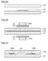
- FIG. 1is a flowchart showing an inter-metal junction technique according to an embodiment of the present disclosure.
- FIGS. 2A-2Care cross-sectional views showing the inter-metal junction technique of the embodiment in the order of process steps.
- FIG. 3is a plan view corresponding to FIG. 2C .
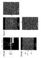
- FIGS. 4A-4Care scanning electron micrographs showing cross sections of a joined body in the inter-metal junction technique of the embodiment.
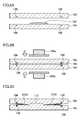
- FIGS. 5A-5Care cross-sectional views showing an inter-metal junction technique according to a second variation of the embodiment in the order of process steps.
- FIG. 6is a cross-sectional view illustrating a power module using the inter-metal junction technique of the embodiment.
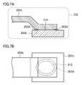
- FIG. 7Ais an enlarged cross-sectional view illustrating a region including a junction portion illustrated in FIG. 6
- FIG. 7Bis an enlarged plan view illustrating the region including the junction portion.
- FIGS. 8A-8Care cross-sectional views illustrating conventional cold welding of metals in the order of process steps.
- FIG. 1 and FIGS. 2A-2C and FIG. 3an oxide film is formed on the surface of each of a first metal plate 101 and a second metal plate 102 .
- an aqueous solution 103 as an example of a solutionis dropped on a region where a junction portion is to be formed (hereinafter referred to as a “junction region”) of a first metal plate (a first junction target member) 101 as an example of a junction target member (step S 01 in FIG. 1 ).
- the aqueous solution 103contains an oxide film remover, an oxidation inhibitor (a rust preventive), and a rheology control (viscosity reducing) agent.
- the content of the aqueous solution 103 except the above-listed materialsis water (H 2 O).
- the junction regionis a region defined to form a junction portion 110 between the first metal plate 101 and the second metal plate 102 illustrated in FIG. 2C .
- the size of the junction regioncan be obtained based on a junction area between metals previously calculated using, for example, existing experimental data.
- the oxide film removeris potassium hydroxide (KOH) having a concentration (mass %) of 2% or less.
- the oxidation inhibitoris diethylethanolamine ((HOCH 2 CH 2 ) 2 NH) having a concentration (mass %) of 2% or less.
- the rheology control agentis polypropylene glycol (PPG) having a concentration (mass %) of 2% or less.
- the oxide film removermay be lithium hydroxide (LiOH), sodium hydroxide (NaOH), formic acid (HCOOH), or acetic acid (CH 3 COOH), instead of potassium hydroxide.
- the oxidation inhibitormay be dicyclohexylamine, instead of diethylethanolamine.
- the rheology control agentmay be polyethylene glycol (PEG) instead of polypropylene glycol.
- the aqueous solution 103only needs to contain the oxide film remover.
- the oxidation inhibitor and the rheology control agentcan be added when necessary.
- the aqueous solution 103preferably contains the oxidation inhibitor in addition to the oxide film remover.
- the oxidation inhibitoris attached to the bare surface exposed by extension of the oxide film remover to the periphery of the junction portion, and reduce oxidation of the bare surface during partial pressure contact between the metal plates 101 and 102 .
- the rheology control agentis used to control viscosity of the aqueous solution 103 to reduce extension of the aqueous solution 103 .
- the oxidation inhibitoris contained in addition to the oxide film remover as in this embodiment, it is necessary to add the rheology control agent to reduce extension of the aqueous solution 103 .
- the amount of the aqueous solution 103 to be droppedcan be greater than or equal to 0.15 ml/mm 2 and less than or equal to 1.5 ml/mm 2 .
- the second metal plate 102is brought into contact with the aqueous solution 103 that has been dropped onto the first metal plate 101 (step S 04 in FIG. 1 ).
- step S 04 in FIG. 1By bringing the second metal plate 102 into contact with the aqueous solution 103 , an oxide film on the second metal plate 102 is removed with the aqueous solution 103 , and a bare surface is exposed on the second metal plate 102 (step S 05 in FIG. 1 ).
- a predetermined loadis applied to regions on the first metal plate 101 and the second metal plate 102 in the vertical direction (i.e., in the direction perpendicular to the principal surface) (step S 06 in FIG. 1 ).
- the predetermined loadis preferably greater than or equal to 10 g/cm 2 and less than or equal to 500 g/cm 2 .
- Preferable values of the loadvary depending on the shapes, dimensions, use, etc. of the metal plates 101 and 102 , and are not limited to the above-described range.
- the period of application of a loadis preferably 80 seconds or less in consideration of productivity.
- Heating of the metal punches 105 a and 105 b to a heating temperatureis previously performed by, for example, an internal heater before application of the load.
- the heating temperature of the metal punches 105 a and 105 bcan be set in the range from 80° C. to 200° C., both inclusive, in consideration of the influence of heat to semiconductor elements, for example. In this manner, heating of the metal punches 105 a and 105 b to the heating temperature ensures high-speed junction between the metal plates 101 and 102 , and evaporates moisture and the oxide film remover in the aqueous solution 103 (step S 07 in FIG. 1 ).
- ultrasonic wavemay be applied to at least one of the metal punches 105 a and 105 b or the metal plates 101 and 102 either concurrently with heating or solely. Then, it becomes possible to ensure high-speed junction, while stirring the aqueous solution 103 such that the concentrations of the oxide film remover and the oxidation inhibitor are uniform in the aqueous solution 103 .
- the junction portion 110is formed on regions of the first metal plate 101 and the second metal plate 102 to which the load was applied, and thereby, the first metal plate 101 and the second metal plate 102 are joined together.
- a joined body constituted by the first metal plate 101 and the second metal plate 102is manufactured (step S 08 in FIG. 1 ).
- the metal plates 101 and 102come to have fillet shapes.
- the fillet shapes of the metal plates 101 and 102 around the junction portion 110fill the clearance between the metal plates 101 and 102 and join the metal plates 101 and 102 together.
- the aqueous solution 103 containing the above-mentioned componentsis used and the metal punches 105 a and 105 b are heated, thereby forming an anti-corrosion film (a rust-inhibiting organic film in a case where the metal plates are made of iron (Fe)) 103 A containing an oxidation inhibitor as a main component around the junction portion 110 (step S 09 in FIG. 1 ).
- the anti-corrosion film 103 Ais a film formed after evaporation of moisture and the oxide film remover in the aqueous solution 103 .
- This anti-corrosion film 103 Ais formed on side surfaces of the fillet shapes of the metal plates 101 and 102 formed around the junction portion 110 . In this manner, formation of the anti-corrosion film 103 A can reduce deterioration of the junction portion 110 due to oxidation and corrosion of an exposed bare surface.
- the distance between the first metal plate 101 and the second metal plate 102 in the junctionis greater than or equal to 0.5 ⁇ m and less than or equal to 100 ⁇ m.
- the reason why the distance of the first metal plate 101 and the second metal plate 102 is greater than or equal to 0.5 ⁇ mis to allow the aqueous solution 103 in an amount necessary for removing the oxide film to be present between the metal plates 101 and 102 .
- the reason why the distance is less than or equal to 100 ⁇ mis to cause the aqueous solution 103 (the anti-corrosion film 103 A after the junction) to flow and stay on the surfaces of the fillet shapes formed on the upper metal plate in the vertical direction (the second metal plate 102 in FIG. 2C ) by utilizing capillary action.
- FIGS. 4A-4Care scanning electron micrographs showing cross sections of a joined body in a case where the first metal plate 101 and the second metal plate 102 are made of copper (Cu). In these micrographs, the amount of the aqueous solution 103 to be dropped is 0.72 ml/mm 2 .
- FIG. 4Bshows a partial cross section of a region 111 a (a center part of the junction portion 110 ) of FIG. 4A enlarged at a magnification of 500 .
- FIG. 4Cshows partial cross sections of a region 111 b (an outer peripheral part of the junction portion 110 ) of FIG. 4A enlarged at magnifications of 500 and 2000, respectively.
- FIG. 4Cincludes cross sections of regions except the junction portion 110 , i.e., regions that are not joined.
- FIG. 4Bshows that the junction portion 110 of the metal plates 101 and 102 is formed as intended.
- FIG. 4Cshows that the peripheral parts of the junction portion 110 of the metal plates 101 and 102 are partially joined together and a clearance is present between the metal plates 101 and 102 .
- the first metal plate 101 and the second metal plate 102may be made of materials except copper (Cu), which is used in this embodiment, by appropriately adjusting the composition of the aqueous solution 103 and conditions for the junction.
- Cucopper
- the first and second metal plates 101 and 102are members constituting a semiconductor device, a metal of at least one of copper (Cu), aluminium (Al), nickel (Ni), or iron (Fe), or an alloy containing one of these element as a main component is often used.
- the metals or the alloymay be of the same type or of different types.
- an aqueous solution 103 suitable for each of the types of the metalsneeds to be used. That is, in a case where oxide films with different properties are formed on the surfaces of metals of different types, an aqueous solution 103 suitable for both types of metals needs to be used.
- plate-shape metalsare used as members to be subjected to metal junction.
- metalsdo not need to have plate-shapes, and may have any shapes that can be joined in general.
- the use of the heated die punches and the aqueous solution containing, for example, the oxide film removerenables easy and electrically stable metal junction to manufacture a joined body.
- Bus bars as rod-shape metal members used as power supply lines instead of wiresare mechanically or electrically joined together with screws in conventional techniques.
- Application of this embodiment to such bus barscan eliminate the necessity of screws to simplify junction processes, and also reduce the weight of electrical equipment using the bus bars.
- the present disclosureis also applicable to a so-called grain boundary junction performed by providing a particle boundary in a junction surface.
- an oxide filmmay be formed under specific conditions after joining the first metal plate 101 and the second metal plate 102 together.
- an oxide filminstead of the anti-corrosion film 103 A formed on the bare surface, oxidation and corrosion can be reduced.
- the first metal plate 101 and the second metal plate 102 that have been joined togetherare exposed to an oxidizing atmosphere (e.g., heated oxygen (O 2 ) atmosphere) and an oxide film is formed on a bare surface formed by an oxide film remover that has flown out from the junction portion 110 , thereby reducing oxidation and corrosion without using the anti-corrosion film 103 A described above.
- an oxidizing atmospheree.g., heated oxygen (O 2 ) atmosphere
- the oxide filmcan stabilize the peripheral region of the junction portion 110 , thereby ensuring long-term reliability of a joined body, in a manner similar to the case of using the anti-corrosion film 103 A. That is, in the first variation, long-term reliability of a joined body can be obtained without using an oxidation inhibitor.
- the oxide filmis formed in an additional process step, it is necessary to eliminate the influence of removal of the oxide film by an oxide film remover contained in the aqueous solution 103 .
- heat treatmentmay be performed, for example.
- the oxidation processmay be performed at a heating temperature of 100° C. for a heating period of about one hour, for example.
- FIGS. 5A-5CA second variation of the embodiment will be described with reference to FIGS. 5A-5C .
- a groove (recess) 106is formed on a surface of each of the first metal plate 101 and the second metal plate 102 forming the junction portion 110 to surround the junction portion.
- the groove 106has a diameter greater than or equal to 1.2, and less than or equal to 2, times as large as the pressing diameter of each of the metal punches 105 a and 105 b having circular pressing surfaces.
- the groove 106 surrounding the junction regionmay have an area about 1.25 times as large as the area of the junction region.
- the area of the groove 106is the area where a sufficient amount of the aqueous solution 103 to be dropped to remove an oxide film on the junction region extends.
- the shape (in plan view) of the groove 106is not specifically limited as long as the groove 106 has a continuous ring shape.
- the groove 106is formed to be circular.
- the depth of the groove 106is a half or less of the thickness of each of the metal plates 101 and 102 .
- the reason why the depth of the groove 106 is a half or less of the thickness of each of the metal plates 101 and 102is that, if the depth of the groove 106 exceeds a half of the thickness of each of the metal plates 101 and 102 , the strengths of the metal plates 101 and 102 cannot be maintained.
- the groove 106can be formed by etching using an acid solution, for example. Then, the aqueous solution 103 is dropped on the junction region on the first metal plate 101 (step S 01 in FIG. 1 ).
- the second metal plate 102is placed on the first metal plate 101 on which the aqueous solution 103 has been dropped, and is brought into contact with the first metal plate 101 (step S 04 in FIG. 1 ).
- the aqueous solution 103flows into the groove 106 , and thus, the aqueous solution 103 does not easily expand on the contact interface between the first metal plate 101 and the second metal plate 102 .
- the metal plates 101 and 102are used as members constituting a semiconductor device, it is possible to prevent the aqueous solution 103 from permeating functional elements or other elements constituting the semiconductor device to adversely affect the functional elements or other elements.
- a predetermined loadis applied to regions of the first metal plate 101 and the second metal plate 102 in the vertical direction (i.e., in the direction perpendicular to the principal surface), thereby forming a junction portion 110 in the first metal plate 101 and the second metal plate 102 , as illustrated in FIG. 5C .
- the groove (recess) 106for preventing extension of the aqueous solution 103 to the periphery of the junction region of each of the metal plates 101 and 102 .
- the groove 106may be formed on at least one of the metal plates 101 and 102 .
- the groove 106 formed only on the lower first metal plate 101 in the vertical directioncan substantially prevent extension of the aqueous solution 103 .
- a protrusionsurrounding the junction region and projecting from the junction surface may be provided on at least one of the first metal plate 101 or the second metal plate 102 .
- the protrusionblocks a flow of the aqueous solution 103 , thereby preventing unnecessary extension of the aqueous solution 103 .
- the protrusioncan be formed by pressing, for example.
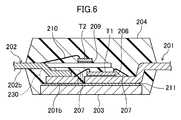
- a power module (power semiconductor device) to be incorporated in an inverter controllerwill be described with reference to FIGS. 6 , 7 A, and 7 B.
- a power moduleincludes a first lead frame 201 holding a power device T 1 on a first die pad, a second lead frame 202 holding a control device T 2 on a second die pad, a heat dissipating plate 203 fixed to the lower surface of the first lead frame 201 with an insulating sheet 211 interposed therebetween, and a housing 204 of an encapsulating resin.
- the housing 204covers one end of the first lead frame 201 including the power device T 1 and an end of the second lead frame 202 including the control device T 2 , exposes the lower surface of the heat dissipating plate 203 .
- At least part of the first die padoverlaps with the second die pad in plan view in order to reduce the size of the power module.
- At least part of the power device T 1also overlaps with the control device T 2 in plan view.
- one of leads of the first lead frame 201is a relay lead 201 b for a power device (hereinafter referred to as a power device relay lead 201 b ).
- One of leads of the second lead frame 202is a relay lead 202 b for a control device (hereinafter referred to as control device relay lead 202 b ).
- ends of the power device relay lead 201 b and the control device relay lead 202 bare joined together by a junction portion (an alloy layer) 212 according to the present disclosure to form a joined body, thereby manufacturing a power module.
- a power module according to the present disclosurewill be specifically described hereinafter.
- the first lead frame 201is made of, for example, a metal having a high conductivity such as copper (Cu).
- the power device T 1may be, for example, an insulated gate bipolar transistor (IGBT) or a metal oxide semiconductor field-effect transistor (a power MOSFET).
- IGBTinsulated gate bipolar transistor
- MOSFETmetal oxide semiconductor field-effect transistor
- the power device T 1is fixed to the upper surface of a first die pad of the first lead frame 201 with a brazing material 206 . Bonding pads (not shown) of the power device T 1 are electrically connected to leads of the first lead frame 201 by wires 207 of, for example, aluminium (Al).
- the heat dissipating plate 203can be made of, for example, copper (Cu) or aluminium (Al).
- the insulating sheet 211 sandwiched between the heat dissipating plate 203 and the die padsis made of an insulating material having thermal conductivity.
- the second lead frame 202is made of, for example, copper (Cu) or an ally 42 (Fe-42% Ni).
- the control device T 2is a semiconductor chip for controlling the power device T 1 , and includes, for example, a drive circuit and an overcurrent protection circuit.
- the control device T 2is fixed to the upper surface of the second die pad of the second lead frame 202 by, for example, a silver (Ag) paste 209 . Bonding pads (not shown) of the control device T 2 are electrically connected to leads of the second lead frame 202 by wires 210 of gold (Au).
- the power device relay lead 201 bis provided in the first lead frame 201
- the control device relay lead 202 bis provided in the second lead frame 202
- the power device relay lead 201 b and the control device relay lead 202 bare joined together by the junction portion 212 using an inter-metal junction technique according to the present disclosure.
- the power device relay lead 201 b and the control device relay lead 202 bare joined together by metal junction using an aqueous solution containing an oxide film remover, an oxidation inhibitor, and a rheology control agent, for example, thereby electrically connecting the leads 201 b and 202 b together.
- a rust-inhibiting organic film 203 Ais formed around the junction portion 212 .
- a joined body, a power semiconductor device, and manufacturing methods of the joined body and the power semiconductor device according to the present disclosureenable electrically stable junction by utilizing mechanical pressure contact between metals, for example, and are useful for a wide range of fields such as lead frames for semiconductor devices and bus bars for batteries.
Landscapes
- Engineering & Computer Science (AREA)
- Mechanical Engineering (AREA)
- Physics & Mathematics (AREA)
- Condensed Matter Physics & Semiconductors (AREA)
- General Physics & Mathematics (AREA)
- Computer Hardware Design (AREA)
- Microelectronics & Electronic Packaging (AREA)
- Power Engineering (AREA)
- Manufacturing & Machinery (AREA)
- Pressure Welding/Diffusion-Bonding (AREA)
- Chemical Treatment Of Metals (AREA)
Abstract
Description
Claims (8)
Applications Claiming Priority (3)
| Application Number | Priority Date | Filing Date | Title |
|---|---|---|---|
| JP2011183714 | 2011-08-25 | ||
| JP2011-183714 | 2011-08-25 | ||
| PCT/JP2012/005039WO2013027354A1 (en) | 2011-08-25 | 2012-08-08 | Bonded body, power semiconductor device and method for manufacturing bonded body and power semiconductor device |
Publications (2)
| Publication Number | Publication Date |
|---|---|
| US20130221502A1 US20130221502A1 (en) | 2013-08-29 |
| US9013029B2true US9013029B2 (en) | 2015-04-21 |
Family
ID=47746126
Family Applications (1)
| Application Number | Title | Priority Date | Filing Date |
|---|---|---|---|
| US13/882,436ActiveUS9013029B2 (en) | 2011-08-25 | 2012-08-08 | Joined body having an anti-corrosion film formed around a junction portion, and a semiconductor device having the same |
Country Status (5)
| Country | Link |
|---|---|
| US (1) | US9013029B2 (en) |
| EP (2) | EP3002075B1 (en) |
| JP (1) | JP5830704B2 (en) |
| CN (1) | CN103228394B (en) |
| WO (1) | WO2013027354A1 (en) |
Families Citing this family (3)
| Publication number | Priority date | Publication date | Assignee | Title |
|---|---|---|---|---|
| CN105336631B (en)* | 2014-06-04 | 2019-03-01 | 恩智浦美国有限公司 | The semiconductor device assembled using two lead frames |
| CN104022176B (en)* | 2014-06-24 | 2016-04-20 | 天津三安光电有限公司 | The preparation method of four-junction solar cell |
| JP6561481B2 (en)* | 2015-02-02 | 2019-08-21 | 国立大学法人群馬大学 | Method of joining steel materials |
Citations (39)
| Publication number | Priority date | Publication date | Assignee | Title |
|---|---|---|---|---|
| US2868863A (en)* | 1954-01-05 | 1959-01-13 | Kaiser Aluminium Chem Corp | Aluminum to copper connection |
| US4188438A (en) | 1975-06-02 | 1980-02-12 | National Semiconductor Corporation | Antioxidant coating of copper parts for thermal compression gang bonding of semiconductive devices |
| US4318966A (en)* | 1980-03-31 | 1982-03-09 | Imperial Chemical Industries Limited | Welded structures |
| GB2097298A (en) | 1981-03-30 | 1982-11-03 | Tokyo Shibaura Electric Co | Jointing by cold pressing |
| US4622116A (en)* | 1983-11-25 | 1986-11-11 | General Electric Company | Process for electrodepositing mica on coil or bar connections and resulting products |
| US4751146A (en)* | 1985-07-09 | 1988-06-14 | Showa Denko Kabushiki Kaisha | Printed circuit boards |
| JPH09232367A (en) | 1996-02-21 | 1997-09-05 | Nec Corp | Manufacture of semiconductor device |
| US5695863A (en)* | 1994-06-09 | 1997-12-09 | U.S. Philips Corporation | Magneto-optical recording medium |
| US5922850A (en)* | 1990-11-02 | 1999-07-13 | Devor Nurseries Inc | Rose plant named Devtinta |
| US6160342A (en)* | 1997-04-23 | 2000-12-12 | Ngk Spark Plug Co., Ltd. | Resistor-incorporated spark plug and manufacturing method of resistor-incorporated spark plug |
| US6291094B1 (en)* | 1998-05-07 | 2001-09-18 | Toyota Jidosha Kabushiki Kaisha | Separator for fuel cell, fuel cell incorporating the same, and method of production of the same |
| US6410365B1 (en)* | 1998-06-01 | 2002-06-25 | Hitachi, Ltd. | Semiconductor device with two stacked chips in one resin body and method of producing |
| US6515218B1 (en)* | 1999-11-22 | 2003-02-04 | Canon Kabushiki Kaisha | Photovoltaic element, process for the production thereof, method for removing a cover portion of a covered wire, and method for joining a covered wire and a conductor |
| US6524698B1 (en)* | 1990-09-27 | 2003-02-25 | Helmuth Schmoock | Fluid impermeable foil |
| US6649282B1 (en)* | 1999-03-19 | 2003-11-18 | Nippon Steel Corporation | Surface treated steel product prepared by tin-based plating or aluminum-based plating |
| JP2004146731A (en) | 2002-10-28 | 2004-05-20 | Mitsubishi Electric Corp | Method for manufacturing multilayer wiring substrate |
| JP2004273230A (en) | 2003-03-07 | 2004-09-30 | Okutekku:Kk | Metal joining method |
| US6884390B1 (en)* | 2001-05-31 | 2005-04-26 | Flexcon Company, Inc. | Method and system for inhibiting corrosion involving the transfer of thin films |
| US20060027633A1 (en) | 2004-08-04 | 2006-02-09 | Denso Corporation | Metal bonding method |
| US20060134501A1 (en)* | 2004-11-25 | 2006-06-22 | Lee Jong-Ki | Separator for fuel cell, method for preparing the same, and fuel cell stack comprising the same |
| US7115324B1 (en) | 2003-08-29 | 2006-10-03 | Alcoa Inc. | Method of combining welding and adhesive bonding for joining metal components |
| JP2006334562A (en) | 2005-06-06 | 2006-12-14 | Kenichi Suzuki | Dispersion of magnetic material particle having metal chelate compound on surface |
| JP2006334652A (en) | 2005-06-03 | 2006-12-14 | Ebara Corp | Metal joining method |
| JP2007090394A (en) | 2005-09-29 | 2007-04-12 | Tokyo Institute Of Technology | Method for joining metals |
| JP2008229658A (en) | 2007-03-20 | 2008-10-02 | Nissan Motor Co Ltd | Joining method and structure of dissimilar metals |
| US20080251062A1 (en)* | 2004-07-14 | 2008-10-16 | Toshihiro Dodo | Heat Cloth and Process for Producing the Same |
| US20080283038A1 (en)* | 2004-07-14 | 2008-11-20 | Mycoal Products Corporation | Heat Generating Body |
| US20090053553A1 (en)* | 2007-08-24 | 2009-02-26 | Kabushiki Kaisha Kobe Seiko Sho (Kobe Steel, Ltd.) | Conductive material for a connecting part |
| US20090068452A1 (en) | 2007-09-12 | 2009-03-12 | Seiko Epson Corporation | Base member with bonding film, bonding method and bonded body |
| US20090183825A1 (en) | 2008-01-23 | 2009-07-23 | Seiko Epson Corporation | Method of forming bonded body and bonded body |
| JP2010089993A (en) | 2008-10-08 | 2010-04-22 | Ngk Insulators Ltd | Method for joining two members, and joined body |
| US7736730B2 (en)* | 2000-10-11 | 2010-06-15 | Chemetall Gmbh | Method for pretreating and/or coating metallic surfaces with a paint-like coating prior to forming and use of substrates coated in this way |
| JP2010277754A (en) | 2009-05-27 | 2010-12-09 | Micro Denshi Kk | Electrical component connection method and connection device |
| US20110118655A1 (en)* | 2009-11-13 | 2011-05-19 | Ali Fassih | Galvanic skin treatment device |
| US20110206943A1 (en)* | 2010-02-25 | 2011-08-25 | Technical Materials Inc. | Methods for creating side-by-side metallic bonds between different materials using solid-phase bonding and the products produced thereby |
| JP2011210968A (en) | 2010-03-30 | 2011-10-20 | Fujifilm Corp | Multilayer circuit board |
| US20110287336A1 (en)* | 2008-11-25 | 2011-11-24 | Nissan Motor Co., Ltd. | Electrical conductive member and polymer electrolyte fuel cell using the same |
| US20110310498A1 (en)* | 2010-06-17 | 2011-12-22 | Ability Enterprise Co., Ltd. | Lens Device |
| US20120258281A1 (en) | 2009-12-25 | 2012-10-11 | Furukawa Electric Co., Ltd. | Copper foil and method for producing copper foil |
Family Cites Families (4)
| Publication number | Priority date | Publication date | Assignee | Title |
|---|---|---|---|---|
| JPS5952031A (en) | 1982-09-16 | 1984-03-26 | Kubota Ltd | Excavating working vehicle |
| CN100471608C (en)* | 2004-08-04 | 2009-03-25 | 株式会社电装 | Metal Joining Method |
| JP2006095534A (en)* | 2004-09-28 | 2006-04-13 | Ebara Corp | Joining method and its apparatus |
| JP4961532B2 (en)* | 2006-07-25 | 2012-06-27 | 日産自動車株式会社 | Method and apparatus for joining dissimilar metals |
- 2012
- 2012-08-08WOPCT/JP2012/005039patent/WO2013027354A1/enactiveApplication Filing
- 2012-08-08JPJP2013505019Apatent/JP5830704B2/ennot_activeExpired - Fee Related
- 2012-08-08EPEP15195652.1Apatent/EP3002075B1/ennot_activeNot-in-force
- 2012-08-08CNCN201280003849.3Apatent/CN103228394B/ennot_activeExpired - Fee Related
- 2012-08-08USUS13/882,436patent/US9013029B2/enactiveActive
- 2012-08-08EPEP12826272.2Apatent/EP2650074A4/ennot_activeWithdrawn
Patent Citations (40)
| Publication number | Priority date | Publication date | Assignee | Title |
|---|---|---|---|---|
| US2868863A (en)* | 1954-01-05 | 1959-01-13 | Kaiser Aluminium Chem Corp | Aluminum to copper connection |
| US4188438A (en) | 1975-06-02 | 1980-02-12 | National Semiconductor Corporation | Antioxidant coating of copper parts for thermal compression gang bonding of semiconductive devices |
| US4318966A (en)* | 1980-03-31 | 1982-03-09 | Imperial Chemical Industries Limited | Welded structures |
| GB2097298A (en) | 1981-03-30 | 1982-11-03 | Tokyo Shibaura Electric Co | Jointing by cold pressing |
| JPS5952031B2 (en) | 1981-03-30 | 1984-12-17 | 株式会社東芝 | Cold welding method |
| US4622116A (en)* | 1983-11-25 | 1986-11-11 | General Electric Company | Process for electrodepositing mica on coil or bar connections and resulting products |
| US4751146A (en)* | 1985-07-09 | 1988-06-14 | Showa Denko Kabushiki Kaisha | Printed circuit boards |
| US6524698B1 (en)* | 1990-09-27 | 2003-02-25 | Helmuth Schmoock | Fluid impermeable foil |
| US5922850A (en)* | 1990-11-02 | 1999-07-13 | Devor Nurseries Inc | Rose plant named Devtinta |
| US5695863A (en)* | 1994-06-09 | 1997-12-09 | U.S. Philips Corporation | Magneto-optical recording medium |
| JPH09232367A (en) | 1996-02-21 | 1997-09-05 | Nec Corp | Manufacture of semiconductor device |
| US6160342A (en)* | 1997-04-23 | 2000-12-12 | Ngk Spark Plug Co., Ltd. | Resistor-incorporated spark plug and manufacturing method of resistor-incorporated spark plug |
| US6291094B1 (en)* | 1998-05-07 | 2001-09-18 | Toyota Jidosha Kabushiki Kaisha | Separator for fuel cell, fuel cell incorporating the same, and method of production of the same |
| US6410365B1 (en)* | 1998-06-01 | 2002-06-25 | Hitachi, Ltd. | Semiconductor device with two stacked chips in one resin body and method of producing |
| US6649282B1 (en)* | 1999-03-19 | 2003-11-18 | Nippon Steel Corporation | Surface treated steel product prepared by tin-based plating or aluminum-based plating |
| US6515218B1 (en)* | 1999-11-22 | 2003-02-04 | Canon Kabushiki Kaisha | Photovoltaic element, process for the production thereof, method for removing a cover portion of a covered wire, and method for joining a covered wire and a conductor |
| US7736730B2 (en)* | 2000-10-11 | 2010-06-15 | Chemetall Gmbh | Method for pretreating and/or coating metallic surfaces with a paint-like coating prior to forming and use of substrates coated in this way |
| US6884390B1 (en)* | 2001-05-31 | 2005-04-26 | Flexcon Company, Inc. | Method and system for inhibiting corrosion involving the transfer of thin films |
| JP2004146731A (en) | 2002-10-28 | 2004-05-20 | Mitsubishi Electric Corp | Method for manufacturing multilayer wiring substrate |
| JP2004273230A (en) | 2003-03-07 | 2004-09-30 | Okutekku:Kk | Metal joining method |
| US7115324B1 (en) | 2003-08-29 | 2006-10-03 | Alcoa Inc. | Method of combining welding and adhesive bonding for joining metal components |
| US20080251062A1 (en)* | 2004-07-14 | 2008-10-16 | Toshihiro Dodo | Heat Cloth and Process for Producing the Same |
| US20080283038A1 (en)* | 2004-07-14 | 2008-11-20 | Mycoal Products Corporation | Heat Generating Body |
| US20060027633A1 (en) | 2004-08-04 | 2006-02-09 | Denso Corporation | Metal bonding method |
| US20060134501A1 (en)* | 2004-11-25 | 2006-06-22 | Lee Jong-Ki | Separator for fuel cell, method for preparing the same, and fuel cell stack comprising the same |
| JP2006334652A (en) | 2005-06-03 | 2006-12-14 | Ebara Corp | Metal joining method |
| JP2006334562A (en) | 2005-06-06 | 2006-12-14 | Kenichi Suzuki | Dispersion of magnetic material particle having metal chelate compound on surface |
| JP2007090394A (en) | 2005-09-29 | 2007-04-12 | Tokyo Institute Of Technology | Method for joining metals |
| JP2008229658A (en) | 2007-03-20 | 2008-10-02 | Nissan Motor Co Ltd | Joining method and structure of dissimilar metals |
| US20090053553A1 (en)* | 2007-08-24 | 2009-02-26 | Kabushiki Kaisha Kobe Seiko Sho (Kobe Steel, Ltd.) | Conductive material for a connecting part |
| US20090068452A1 (en) | 2007-09-12 | 2009-03-12 | Seiko Epson Corporation | Base member with bonding film, bonding method and bonded body |
| US20090183825A1 (en) | 2008-01-23 | 2009-07-23 | Seiko Epson Corporation | Method of forming bonded body and bonded body |
| JP2010089993A (en) | 2008-10-08 | 2010-04-22 | Ngk Insulators Ltd | Method for joining two members, and joined body |
| US20110287336A1 (en)* | 2008-11-25 | 2011-11-24 | Nissan Motor Co., Ltd. | Electrical conductive member and polymer electrolyte fuel cell using the same |
| JP2010277754A (en) | 2009-05-27 | 2010-12-09 | Micro Denshi Kk | Electrical component connection method and connection device |
| US20110118655A1 (en)* | 2009-11-13 | 2011-05-19 | Ali Fassih | Galvanic skin treatment device |
| US20120258281A1 (en) | 2009-12-25 | 2012-10-11 | Furukawa Electric Co., Ltd. | Copper foil and method for producing copper foil |
| US20110206943A1 (en)* | 2010-02-25 | 2011-08-25 | Technical Materials Inc. | Methods for creating side-by-side metallic bonds between different materials using solid-phase bonding and the products produced thereby |
| JP2011210968A (en) | 2010-03-30 | 2011-10-20 | Fujifilm Corp | Multilayer circuit board |
| US20110310498A1 (en)* | 2010-06-17 | 2011-12-22 | Ability Enterprise Co., Ltd. | Lens Device |
Non-Patent Citations (2)
| Title |
|---|
| Chinese Office Action and Search Report issued in Chinese Application No. 201280003849.3 dated Dec. 22, 2014, with English Translation. |
| International Search Report issued in International Patent Application No. PCT/JP2012/005039 mailed on Nov. 13, 2012. |
Also Published As
| Publication number | Publication date |
|---|---|
| JP5830704B2 (en) | 2015-12-09 |
| WO2013027354A1 (en) | 2013-02-28 |
| EP3002075B1 (en) | 2017-02-01 |
| CN103228394B (en) | 2016-05-25 |
| US20130221502A1 (en) | 2013-08-29 |
| EP2650074A4 (en) | 2014-06-18 |
| EP3002075A1 (en) | 2016-04-06 |
| JPWO2013027354A1 (en) | 2015-03-05 |
| CN103228394A (en) | 2013-07-31 |
| EP2650074A1 (en) | 2013-10-16 |
Similar Documents
| Publication | Publication Date | Title |
|---|---|---|
| US8299600B2 (en) | Semiconductor device and manufacturing method thereof | |
| CN202454546U (en) | Semiconductor device | |
| TWI532104B (en) | Manufacturing method of semiconductor device and manufacturing method of electronic device | |
| US8975117B2 (en) | Semiconductor device using diffusion soldering | |
| CN106971996B (en) | Semiconductor device with a plurality of transistors | |
| CN105247666B (en) | Semiconductor device and its manufacture method | |
| US20120248592A1 (en) | Lead component and method for manufacturing the same, and semiconductor package | |
| US12394769B2 (en) | Batch soldering of different elements in power module | |
| CN107104056B (en) | Manufacturing method of semiconductor device | |
| CN112786468B (en) | Preform Diffusion Bonding | |
| US9013029B2 (en) | Joined body having an anti-corrosion film formed around a junction portion, and a semiconductor device having the same | |
| US12009332B2 (en) | Semiconductor device having high yield strength intermediate plate | |
| JP7549638B2 (en) | Method for manufacturing semiconductor device | |
| JP2010097963A (en) | Circuit board and method for manufacturing the same, and electronic component module | |
| US20140374926A1 (en) | Semiconductor device | |
| JP5579148B2 (en) | Power semiconductor device | |
| CN112786469B (en) | Bulk diffusion welding and electronic device produced by bulk diffusion welding | |
| JP5734493B2 (en) | Power semiconductor device | |
| HK1240706A1 (en) | Semiconductor device |
Legal Events
| Date | Code | Title | Description |
|---|---|---|---|
| AS | Assignment | Owner name:PANASONIC CORPORATION, JAPAN Free format text:ASSIGNMENT OF ASSIGNORS INTEREST;ASSIGNORS:MINAMIO, MASANORI;SASAOKA, TATSUO;REEL/FRAME:030639/0016 Effective date:20130401 | |
| AS | Assignment | Owner name:PANASONIC INTELLECTUAL PROPERTY MANAGEMENT CO., LTD., JAPAN Free format text:ASSIGNMENT OF ASSIGNORS INTEREST;ASSIGNOR:PANASONIC CORPORATION;REEL/FRAME:034194/0143 Effective date:20141110 Owner name:PANASONIC INTELLECTUAL PROPERTY MANAGEMENT CO., LT Free format text:ASSIGNMENT OF ASSIGNORS INTEREST;ASSIGNOR:PANASONIC CORPORATION;REEL/FRAME:034194/0143 Effective date:20141110 | |
| STCF | Information on status: patent grant | Free format text:PATENTED CASE | |
| FEPP | Fee payment procedure | Free format text:PAYOR NUMBER ASSIGNED (ORIGINAL EVENT CODE: ASPN); ENTITY STATUS OF PATENT OWNER: LARGE ENTITY | |
| MAFP | Maintenance fee payment | Free format text:PAYMENT OF MAINTENANCE FEE, 4TH YEAR, LARGE ENTITY (ORIGINAL EVENT CODE: M1551); ENTITY STATUS OF PATENT OWNER: LARGE ENTITY Year of fee payment:4 | |
| AS | Assignment | Owner name:PANASONIC INTELLECTUAL PROPERTY MANAGEMENT CO., LTD., JAPAN Free format text:CORRECTIVE ASSIGNMENT TO CORRECT THE ERRONEOUSLY FILED APPLICATION NUMBERS 13/384239, 13/498734, 14/116681 AND 14/301144 PREVIOUSLY RECORDED ON REEL 034194 FRAME 0143. ASSIGNOR(S) HEREBY CONFIRMS THE ASSIGNMENT;ASSIGNOR:PANASONIC CORPORATION;REEL/FRAME:056788/0362 Effective date:20141110 | |
| MAFP | Maintenance fee payment | Free format text:PAYMENT OF MAINTENANCE FEE, 8TH YEAR, LARGE ENTITY (ORIGINAL EVENT CODE: M1552); ENTITY STATUS OF PATENT OWNER: LARGE ENTITY Year of fee payment:8 |