US9012938B2 - High reflective substrate of light emitting devices with improved light output - Google Patents
High reflective substrate of light emitting devices with improved light outputDownload PDFInfo
- Publication number
- US9012938B2 US9012938B2US12/757,179US75717910AUS9012938B2US 9012938 B2US9012938 B2US 9012938B2US 75717910 AUS75717910 AUS 75717910AUS 9012938 B2US9012938 B2US 9012938B2
- Authority
- US
- United States
- Prior art keywords
- light
- substrate
- reflective coating
- reflective
- light emitting
- Prior art date
- Legal status (The legal status is an assumption and is not a legal conclusion. Google has not performed a legal analysis and makes no representation as to the accuracy of the status listed.)
- Active
Links
Images


Classifications
- H01L33/60—
- H—ELECTRICITY
- H10—SEMICONDUCTOR DEVICES; ELECTRIC SOLID-STATE DEVICES NOT OTHERWISE PROVIDED FOR
- H10H—INORGANIC LIGHT-EMITTING SEMICONDUCTOR DEVICES HAVING POTENTIAL BARRIERS
- H10H20/00—Individual inorganic light-emitting semiconductor devices having potential barriers, e.g. light-emitting diodes [LED]
- H10H20/80—Constructional details
- H10H20/85—Packages
- H10H20/855—Optical field-shaping means, e.g. lenses
- H10H20/856—Reflecting means
- H—ELECTRICITY
- H01—ELECTRIC ELEMENTS
- H01L—SEMICONDUCTOR DEVICES NOT COVERED BY CLASS H10
- H01L25/00—Assemblies consisting of a plurality of semiconductor or other solid state devices
- H01L25/03—Assemblies consisting of a plurality of semiconductor or other solid state devices all the devices being of a type provided for in a single subclass of subclasses H10B, H10D, H10F, H10H, H10K or H10N, e.g. assemblies of rectifier diodes
- H01L25/04—Assemblies consisting of a plurality of semiconductor or other solid state devices all the devices being of a type provided for in a single subclass of subclasses H10B, H10D, H10F, H10H, H10K or H10N, e.g. assemblies of rectifier diodes the devices not having separate containers
- H01L25/075—Assemblies consisting of a plurality of semiconductor or other solid state devices all the devices being of a type provided for in a single subclass of subclasses H10B, H10D, H10F, H10H, H10K or H10N, e.g. assemblies of rectifier diodes the devices not having separate containers the devices being of a type provided for in group H10H20/00
- H01L25/0753—Assemblies consisting of a plurality of semiconductor or other solid state devices all the devices being of a type provided for in a single subclass of subclasses H10B, H10D, H10F, H10H, H10K or H10N, e.g. assemblies of rectifier diodes the devices not having separate containers the devices being of a type provided for in group H10H20/00 the devices being arranged next to each other
- H—ELECTRICITY
- H01—ELECTRIC ELEMENTS
- H01L—SEMICONDUCTOR DEVICES NOT COVERED BY CLASS H10
- H01L2924/00—Indexing scheme for arrangements or methods for connecting or disconnecting semiconductor or solid-state bodies as covered by H01L24/00
- H—ELECTRICITY
- H01—ELECTRIC ELEMENTS
- H01L—SEMICONDUCTOR DEVICES NOT COVERED BY CLASS H10
- H01L2924/00—Indexing scheme for arrangements or methods for connecting or disconnecting semiconductor or solid-state bodies as covered by H01L24/00
- H01L2924/0001—Technical content checked by a classifier
- H01L2924/0002—Not covered by any one of groups H01L24/00, H01L24/00 and H01L2224/00
Definitions
- the present inventionrelates generally to light emitting devices, and more particularly to light emitting devices with highly reflective properties for improved light output.
- LEDLight emitting diodes
- LED or LEDsare solid state devices that convert electric energy to light and generally comprise an active region of semiconductor material sandwiched between two oppositely doped layers of semiconductor material. When a bias is applied across the doped layers, holes and electrons are injected into the active region where they recombine to generate light. Light is emitted from the active layer and from all surfaces of the LED.
- LEDscan be fabricated to emit light in various colors. However, conventional LEDs cannot generate white light from their active layers. Light from a blue emitting LED has been converted to white light by surrounding the LED with a yellow phosphor, polymer or dye, with a typical phosphor being cerium-doped yttrium aluminum garnet (Ce:YAG). The surrounding phosphor material “downconverts” the energy of some of the LED's blue light which increases the wavelength of the light, changing its color to yellow. Some of the blue light passes through the phosphor without being changed while a portion of the light is downconverted to yellow. The LED emits both blue and yellow light, which combine to provide a white light. In another approach light from a violet or ultraviolet emitting LED has been converted to white light by surrounding the LED with multicolor phosphors or dyes.
- lighting moduleshave become available to further increase luminous flux output.
- Both single and multi-chip moduleshave become available, with a single-chip module generally comprising a single package with a single LED.
- Multi-chip lighting modulestypically comprise a single package with a plurality of LEDs. These lighting modules, particularly the multi-chip modules, generally allow for high output of light emission.
- the emitted light from the device chip(s)may be largely non-directional and non-uniform, which can negatively impact the emission and optical efficiency of a lighting module.
- a light diffusion lens, light scattering particles, and/or phosphor particlesare disposed over the chip(s) to assist in achieving more uniform light emission.
- a fraction of brightnesscan be lost when utilizing such means, largely due to back-emission from the emitter, or scattering and back-reflection of light from a light diffusion lens, light scattering particles, and phosphor particles.
- reflective materialshave been disposed on the substrate of various light emitting devices.
- the reflective materialsmay be disposed on only portions of the substrate, or may be disposed as a reflective layer on the substrate.
- light-reflective, white printed circuit board (PCB) and/or substrate technologyhas been developed.
- the materials used for this existing technologyare generally epoxy-based. Epoxy contains free radicals that may yellow during prolonged use and/or common fabrication steps known in the art, such as reflow soldering. Epoxy materials may also degrade in the presence of blue light.
- the present inventionprovides light emitting devices and methods directed to improved light output.
- One embodimentcomprises a light emitting device with a substrate, a reflective layer at least partially covering the substrate, and one or more light emitting diode chips disposed on the substrate.
- the reflective layeris substantially non-yellowing.
- a light emitting devicecomprising a substrate and a reflective coating at least partially covering the substrate.
- the reflective coatingcomprises a material that is substantially resistant to discoloration over time.
- One or more light emitting diode (LED) chipsare disposed on the substrate.
- One embodiment of a light emitting devicecomprises a substrate with a stable reflective coating at least partially covering the substrate.
- the reflective coatingcan comprise a silicone carrier with light reflective particles dispersed in the carrier.
- One or more LED chipscan be disposed on the substrate and a light diffusion lens can be disposed on the substrate and over the LED chips.
- a light emitting devicecomprises a substrate, and one or more LED chips disposed on the substrate.
- a light diffusion lensis disposed on the substrate and surrounding the LED chips, with one or more microspheres dispersed in the light diffusion lens.
- a stable reflective coatingis included at least partially covering the substrate.
- One embodiment of a method for producing a light emitting devicecomprises providing a substrate and mounting LED chips to the substrate.
- a reflective, discoloration resistant coatingis applied on at least a portion of the top surface of the substrate, with the coating comprising a carrier with reflective particles dispersed in the carrier.
- FIG. 1is a schematic side view of a portion of one embodiment of a light emitting device according to the present invention
- FIG. 2is a schematic side view of the light emitting device of FIG. 1 with a lens
- FIG. 3is a schematic side view of a portion of another embodiment of a light emitting device according to the present invention.
- FIG. 4is a schematic side view of the light emitting device of FIG. 3 with a lens
- FIG. 5is a perspective view of one embodiment of an LED lamp according to the present invention.
- FIG. 6is a top view of a portion of one embodiment of a light emitting device according to the present invention.
- FIG. 7is a top view of a portion of one embodiment of a light emitting device according to the present invention.
- FIG. 8is a top view of a portion of one embodiment of a light emitting device according to the present invention.
- FIG. 9is a schematic side view of a portion of one embodiment of a light emitting device according to the present invention.
- FIG. 10is a schematic view of portion 85 depicted in FIG. 9 ;
- FIG. 11is a schematic side view of a portion of another embodiment of a light emitting device according to the present invention.
- FIG. 12is a schematic side view of a portion of another embodiment of a light emitting device according to the present invention.
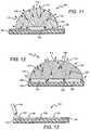
- FIG. 13is a side perspective view of a method for producing a light emitting device according to the present invention.
- the present inventionprovides structures and methods for producing light emitting devices, such as multi-chip LED devices that provide high luminous flux output.
- the electronic elementsmay include one or more circuit boards with light emitting diodes (LEDs), solar cells, photodiodes, laser diodes, and other such optoelectronic elements or combinations of optoelectronic elements.
- LEDslight emitting diodes
- solar cellssolar cells
- photodiodesphotodiodes
- laser diodeslaser diodes
- Other optoelectronic elements or combinations of optoelectronic elementsare generally directed to light emitting devices incorporating LEDs, but it is understood that other light emitting devices may also be used.
- the present inventiongenerally provides devices and methods for light emitting devices for increasing light output using a high reflective coating on a substrate.
- the coatingcan effectively redirect light that is back-emitted from the emitter, back-scattered or reflected by a light diffusion lens, light scattering particles, phosphor particles, and/or microspheres.
- the present inventionmay also provide embodiments for optimal color mixing for white light emitting devices.
- the coating on the substrateshould be robust and stable over time such that it does not degrade in the presence of emitter light or undergo discoloration and/or degradation after elevated temperatures, prolonged use or adverse environmental conditions.
- the reflective layers according to the present inventionare arranged so that the reflective properties of the reflective layer remain substantially constant over time, so that the emitting device retains its emission efficiency over time.
- the coatingcan comprise a carrier with dispersed reflective particles in the carrier, with the carrier and reflective particles having different reflective indexes from one another.
- the reflective particlesare dispersed in the carrier with substantially uniform concentration, although in other embodiments the coating can have different areas of different concentrations to provide different reflective properties.
- the carriercan be substantially transparent to light from the emitter and in some embodiments can be resistant to yellow discoloration; i.e. is substantially non-yellowing.
- Other embodiments of the coating according to the present inventioncan comprise a layer of reflective material on the substrate with a protective coating over the reflective material, with the coating being robust and resistant to discoloration over time.
- the coatingcan also be arranged to protect the underlying reflective layer from environmental conditions such as moisture and oxidation.
- the present inventionis described herein with reference to certain embodiments but it is understood that the invention can be embodied in many different forms and should not be construed as limited to the embodiments set forth herein.
- the present inventionis described below in regards to light emitting devices having substrates coated by a reflective layer typically comprising moldable silicone with interspersed titanium dioxide and/or alumina particles.
- the reflective layermay be coated with other materials for effectively redirecting scattered or back-reflected light.
- the methods according to the present inventioncan also be used for coating other semiconductor devices with different materials.
- single or multiple coatings and/or layerscan be formed on the substrate and on the LED chips.
- a coatingcan include no phosphors, one or more phosphors, scattering particles and/or other materials.
- a coatingmay also comprise a material such as an organic dye that provides down-conversion.
- a materialsuch as an organic dye that provides down-conversion.
- each onecan include different phosphors, different scattering particles, different optical properties, such as transparency, index of refraction, and/or different physical properties, as compared to other layers and/or coatings.
- the present inventionis also described herein with reference to reflective coatings that are color stable or substantially resistant to discoloration over time.
- the coatingcan be resistant to yellow discoloration, and can be described as non-yellowing. It is understood that in other embodiments the coatings according to the present invention can be resistant to other colors of discoloration, including but not limited to reddening or blackening.
- LEDscan have many different semiconductor layers arranged in different ways and can emit many different colors in different embodiments according to the present invention. LED structures, features, and their fabrication and operation are generally known in the art and only briefly discussed herein.
- the layers of the LEDscan be fabricated using known processes, with a suitable process being fabrication using metal organic chemical vapor deposition (MOCVD).
- MOCVDmetal organic chemical vapor deposition
- the layers of the LED chipsgenerally comprise an active layer/region sandwiched between first and second oppositely doped epitaxial layers, all of which are formed successively on a growth substrate. LED chips can be formed on a wafer and then singulated for mounting in a package. It is understood that the growth substrate can remain as part of the final singulated LED or the growth substrate can be fully or partially removed.
- the active regioncan comprise single quantum well (SQW), multiple quantum well (MQW), double heterostructure or super lattice structures.
- SQWsingle quantum well
- MQWmultiple quantum well
- the active region and doped layersmay be fabricated from different material systems, with preferred material systems being Group-III nitride based material systems.
- Group-III nitridesrefer to those semiconductor compounds formed between nitrogen and the elements in the Group III of the periodic table, usually aluminum (Al), gallium (Ga), and indium (In).
- the termalso refers to ternary and quaternary compounds such as aluminum gallium nitride (AlGaN) and aluminum indium gallium nitride (AlInGaN).
- the doped layersare gallium nitride (GaN) and the active region is InGaN.
- the doped layersmay be AlGaN, aluminum gallium arsenide (AlGaAs), aluminum gallium indium arsenide phosphide (AlGaInAsP), aluminium indium galium phosphide (AlInGaP) or zinc oxide (ZnO).
- the growth substratecan be made of many materials such as silicon, glass, sapphire, silicon carbide, aluminum nitride (AlN), gallium nitride (GaN), with a suitable substrate being a 4H polytype of silicon carbide, although other silicon carbide polytypes can also be used including 3C, 6H and 15R polytypes. Silicon carbide has certain advantages, such as a closer crystal lattice match to Group-III nitrides than sapphire and results in Group-III nitride films of higher quality.
- Silicon carbidealso has a very high thermal conductivity so that the total output power of Group-III nitride devices on silicon carbide is not limited by the thermal dissipation of the substrate (as may be the case with some devices formed on sapphire).
- SiC substratesare available from Cree Research, Inc., of Durham, N.C. and methods for producing them are set forth in the scientific literature as well as in a U.S. Pat. Nos. Re. 34,861; 4,946,547; and 5,200,022.
- LEDsmay have vertical or lateral geometry as is known in the art. Those comprising a vertical geometry may have a first contact on a substrate and a second contact on a p-type layer. An electrical signal applied to the first contact spreads into the n-type layer and a signal applied to the second contact spreads into a p-type layer.
- a thin semitransparent current spreading layertypically covers some or all of the p-type layer.
- the second contactcan include such a layer, which is typically a metal such as platinum (Pt) or a transparent conductive oxide such as indium tin oxide (ITO).
- LEDsmay also comprise a lateral geometry, wherein both contacts are on the top of the LEDs.
- a portion of the p-type layer and active regionis removed, such as by etching, to expose a contact mesa on the n-type layer.
- a second lateral n-type contactis provided on the mesa of the n-type layer.
- the contactscan comprise known materials deposited using known deposition techniques.
- first, second, etc.may be used herein to describe various elements, components, regions, and/or sections, these elements, components, regions, and/or sections should not be limited by these terms. These terms are only used to distinguish one element, component, region, or section from another element, component, region, or section. Thus, a first element, component, region, or section discussed below could be termed a second element, component, region, or section without departing from the teachings of the present invention.
- Embodiments of the inventionare described herein with reference to cross-sectional view illustrations that are schematic illustrations of embodiments of the invention. As such, the actual thickness of components can be different, and variations from the shapes of the illustrations as a result, for example, of manufacturing techniques and/or tolerances are expected. Embodiments of the invention should not be construed as limited to the particular shapes of the regions illustrated herein but are to include deviations in shapes that result, for example, from manufacturing. A region illustrated or described as square or rectangular will typically have rounded or curved features due to normal manufacturing tolerances. Thus, the regions illustrated in the figures are schematic in natures and their shapes are not intended to illustrate the precise shape of a region of a device and are not intended to limit the scope of the invention.
- FIGS. 1-4depict a portion of light emitting devices 10 , according to one specific embodiment for use in light emitting devices such as LED lamps.
- the light emitting device portion 10 , 30includes a substrate 12 , which may be formed from a variety of acceptable elements such as described above.
- the substrate 12may include a circuit layer (such as a printed circuit board) that can be printed and fired over all or a portion of the substrate (not shown).
- One LED chip 14(as shown in FIGS. 1-2 ) or a plurality of LED chips 14 (as shown in FIGS. 3-4 ) may be mounted on a portion of the substrate 12 . While it is understood that any acceptable light emitting device may be mounted on the substrate, LEDs constitute part of one embodiment of a light emitting device according to the present invention, and by way of example and not limitation, will be discussed hereinafter.
- the LED chip(s) 14can also comprise a conductive current spreading structure and wire bond pads on the top surface, both of which are made of a conductive material and can be deposited using known methods. Some materials that can be used for these elements include Au, Cu, Ni, In, Al, Ag or combinations thereof and conducting oxides and transparent conducting oxides.
- the current spreading structuremay comprise conductive fingers arranged in a grid with the fingers spaced to enhance current spreading from the pads into the LED's top surface. In operation, an electrical signal may be applied to the pads through a wire bond, and the electrical signal spreads through the fingers of the current spreading structure and the top surface into the LED chip(s) 14 . Current spreading structures are often used in LEDs where the top surface is p-type, but can also be used for n-type materials.
- LED chip(s) 14can be coated with one or more phosphors, with the phosphors absorbing at least some of the LED light and emitting a different wavelength of light such that the LED emits a combination of light from the LED and the phosphor.
- the LED chip(s) 14can be coated with a phosphor using many different methods, with one suitable method being described in U.S. patent application Ser. Nos. 11/656,759 and 11/899,790, both entitled “Wafer Level Phosphor Coating Method and Devices Fabricated Utilizing Method”, and both of which are incorporated herein by reference.
- the LEDscan be coated using other methods such as electrophoretic deposition (EPD), with a suitable EPD method described in U.S. patent application Ser. No. 11/473,089 entitled “Close Loop Electrophoretic Deposition of Semiconductor Devices”, which is also incorporated herein by reference.
- EPDelectrophoretic deposition
- LED chips 14can comprise white emitting LEDs with the desired wavelength of light and the desired color temperature, or the LEDs can comprise different LEDs emitting different colors of light that combine to the desired wavelength of light and the desired color temperature. In both arrangements, the light emitting device 10 can emit white light.
- the substrate 12may be at least partially coated with a high reflective layer/coating 16 to improve reflection of light emitted by the at least one LED chip by reflecting light that is directed toward the substrate that might otherwise be absorbed back at the substrate and/or surrounding structures.
- the high reflective layer/coating 16can be arranged effectively to redirect most or all light that is emitted toward the substrate, or is scattered and/or reflected by a light diffusion lens, light scattering particles and/or phosphor particles toward the surface of the substrate 12 .
- the reflective layer/coating 16is preferably comprised of a carrier with reflective particles that can be arranged in many different ways.
- the reflective particlescan be dispersed throughout the carrier.
- the coating 16can comprise a reflective coating with a layer of carrier material over the reflective coating.
- the carriercan comprise a material having a reflective index differing from the reflective index of the reflective particles and can also be substantially transparent to light from light emitter.
- the carriermay preferably comprise silicone, although it is understood that other materials such as glass, plastics, and/or a polymeric matrix may also be used. It is understood that the carrier can comprise more than one material and can comprise different materials in different layers.
- Siliconeis a suitable material for use in a reflective layer/coating 16 due at least to its durability, flexibility, ability to withstand high temperatures, and resistance to discoloration.
- the silicone coatingcan exhibit non-yellowing characteristics.
- the reflective particlescan be dispersed throughout the carrier and can comprise many different materials such as titanium oxide and/or aluminum oxide particles, although it is understood that other particles with high reflective properties may also be used.
- the particlescan have many different sizes from sub-micron to many micron sizes.
- a combination of reflective particlesmay also be used, and the particles can have a substantially uniform distribution in the carrier or can have areas of differing concentration.
- a silicone carriercomprising titanium dioxide reflective particles with alumina and silica coatings exhibits suitable reflective characteristics in the white light range as well as maintaining suitable reflectivity over time and after exposure to high temperatures.
- the alumina/silica coatingaids in the avoidance of photocatalytic degradation reactions in plastic coatings.
- the substrate 12can comprise a mirror-like material such that it is substantially reflective, and a transparent material can be coated on the substrate. However, the ability to effectively scatter light in such an arrangement can be decreased.
- the coatingcan have different resistance to degradation and discoloration over time.
- the coatingcan experience less than 10% discoloration though up to 5,000 hours of operation.
- the coatingcan experience less than 10% degradation through up to 10,000 hours of operation, while in other embodiments the coating can experience less that 10% discoloration through up to 20,000 hours of operation.
- the coatingcan experience less than 20% discoloration through these different timeframes.
- the reflective layer/coating 16may completely or partially cover portions of the substrate 12 not occupied by the at least one LED chip 14 ; it is understood that as more of the substrate is covered by reflective layer/coating 16 , a larger reflective area is obtained, which can improve the overall reflectivity of the light emitting device 10 , 30 .
- a portion of the substratemay be covered by reflective layer/coating 16 such that substantially all of the substrate 12 outside the perimeter of the at least one LED chip 14 is coated (see, e.g. FIG. 7 ).
- the substratemay be covered by reflective layer/coating 16 such that substantially all of the substrate 12 both outside the perimeter of the LED chip(s) and between each of the LED chips 14 is coated (see, e.g. FIG. 8 ). It is understood that allowing the reflective layer/coating 16 to cover the LED chip 14 can be disadvantageous as it would hinder light from most effectively emanating from the LEDs.
- a light diffusion lens 18may be provided over the substrate 12 and LED chip(s) 14 .
- the lens 18can be formed over the LED chip(s) 14 and substrate 12 using different molding techniques and the lens can be many different shapes depending on the desired shape of the light output.
- One suitable shape as shownis hemispheric, with some examples of alternative shapes being ellipsoid bullet, flat, hex-shaped and square.
- Many different materialscan be used for the lens such as silicones, plastics, epoxies or glass, with a suitable material being compatible with molding processes. Silicone is suitable for molding and provides suitable optical transmission properties. It can also withstand subsequent reflow processes and does not significantly degrade over time. It is understood that the lens 18 can also be textured to improve light extraction or can contain materials such as phosphors or scattering particles.
- the lens arrangementis also easily adapted for use with secondary lens or optics that can be included over the lens by the end user to facilitate beam shaping.
- These secondary lensesare generally known in the art, with many different ones being commercially available.
- the lens 18can also have different features to diffuse or scatter light, such as scattering particles or structures. Particles made from different materials can be used such as titanium dioxide, alumina, silicon carbide, gallium nitride, or glass micro spheres, with the particles dispersed within the lens. Alternatively, or in combination with the scattering particles, air bubbles or an immiscible mixture of polymers having a different index of refraction could be provided within the lens or structured on the lens to provide diffusion.
- the scattering particles or structurescan be dispersed homogeneously throughout the lens 18 or can have different concentrations in different areas of the lens.
- the scattering particlescan be in layers within the lens, or can have different concentrations in relation to the location of the LED chip(s) 14 .
- LED devicessuch as white light sources
- Light diffusion lensescan be advantageously provided to achieve a high degree of color mixing.
- some of the brightness of such a deviceas much as 10-12%, can be lost due to the scattering and back-reflection of light from a light diffusion lens, light scattering particles and structures, and/or phosphor particles.
- Incorporating the reflective layer/coating 16can redirect such scattered and/or back-reflected light, and improve the overall light output of the device by as much as 9% or more.
- FIGS. 2 and 4show light paths 20 , 22 respectively, which illustrate just a few of the paths that light emitted from the one or more LED chips 14 can travel on.
- some of the lightcan be reflected and/or scattered by light scattering means in the light diffusion lens such that it travels back toward the direction of the substrate 12 .
- reflective layer/coating 16Without the inclusion of reflective layer/coating 16 , such light would be reabsorbed by the substrate and/or surrounding structures, which would reduce the overall brightness of the device. However, by including reflective layer/coating 16 , the back-reflected and/or scattered light can be redirected as shown.
- FIG. 5shows one possible embodiment of an LED lamp or luminaire 40 according to the present invention.
- the LED lampcomprises a plurality of LEDs 42 , with reflective layer/coating 16 disposed around the perimeter of the LEDs 42 , between each of the LEDs 42 , or both.
- the lamp 40comprises a wall 46 projecting from the main body of the lamp 40 , with the wall 46 having an inner surface 44 proximate the plurality of LEDs 42 and reflective layer/coating 16 .
- the inner surface 44may be coated with a reflective layer similar to layer/coating 16 so as to further optimize the light output of the lamp 40 . All or portions of inner surface 44 may be coated with a reflective layer depending on the desired emission effects of the lamp 40 .
- Lamp 40also comprises a threaded end portion, enabling lamp 40 to be threadedly engaged with a corresponding threaded socket in a light fixture. While lamp 40 depicts one possible configuration for an LED lamp according to the present invention, it is understood that lamp 40 is provided merely as one possible example, and other shapes, sizes, and configurations for lamps are contemplated by the present invention.
- FIG. 6depicts an overhead view of a portion of a light emitting device 50 according to the present invention.
- This depiction of a light emitting deviceprovides one example of a substrate 12 with a printed circuit board, with substrate 12 not being covered by a reflective layer/coating.
- a plurality of LED chips 14are shown, with various conductive traces and wire bonds allowing electrical connection among and between the various LED chips.
- a light diffusion lens 18is disposed over the substrate 12 and LED chips 14 . Without a reflective layer/coating covering at least a portion of the substrate, light reflected from the LEDs can be scattered and back-reflected by the light diffusion lens and various light scattering particles and/or phosphor particles, with some of the light being absorbed by the substrate and various other structure among the LED chips.
- FIG. 7depicts an overhead view of a portion of a light emitting device 60 according to the present invention.
- This depiction of a light emitting deviceprovides one example of a substrate 12 with a printed circuit board, with substrate 12 being at least partially covered by a reflective layer/coating such that the substrate is covered by layer 16 around the perimeter of a plurality of LED chips 14 .
- the reflective layer/coating 16may coat approximately 60% of the surface area at the top of the substrate 12 , which may increase the overall luminous flux of light emitting device 60 by ⁇ 4-5%.
- the reflective layer/coatingcan cover greater than 60% of the top surface of the substrate. In other embodiments it can cover more than 70% of the surface, and in still other embodiments it can cover more that 80% of the surface.
- FIG. 8depicts an overhead view of a portion of a light emitting device 70 according to the present invention.
- This depiction of a light emitting deviceprovides one example of a substrate 12 with a printed circuit board, with substrate 12 being at least partially covered by a reflective layer/coating such that the substrate is covered by layer 16 around the perimeter of a plurality of LED chips 14 and between each of LED chips 14 .
- the reflective layer/coating 16may coat approximately 86% of the surface area at the top of the substrate 12 , which may increase the overall luminous flux of light emitting device 70 by ⁇ 6.7%. Accordingly, it is understood that by coating the substrate both around the perimeter of the LED chips and between each LED chip, the overall luminous flux improvement of the light emitting device 70 is improved over the luminous flux improvement of light emitting device 60 .
- FIGS. 9-10depict a portion of a light emitting device 80 , 85 according to one specific embodiment for use in light emitting devices such as LED lamps.
- the light emitting device portion 80includes a substrate 82 , which is similar to substrate 12 as described in more detail above.
- the substrate 82may include a circuit layer (such as a printed circuit board) that can be printed and fired over all or a portion of the substrate (not shown).
- At least one LED chip 84 similar to LED chips 14 described abovemay be mounted on a portion of the substrate 82 .
- a light diffusion lens 86 similar to lens 18may be provided over the substrate 82 and LED chip(s) 84 . Similar to lens 18 , lens 86 can have different features to diffuse or scatter light, such as scattering particles 92 or structures (best shown in FIG. 10 ).
- light emitting device 80further comprises microspheres 88 dispersed throughout lens 86 , with the microspheres further enhancing the light mixing of the lens 86 and aiding in the reduction of brightness loss.
- the microspheresare preferably comprised of hollow glass, although it is understood that other suitable materials such as various plastics, metals, or the like may also be used.
- the microspheres 88can be dispersed homogeneously throughout the lens 86 or can have different concentrations in different areas of the lens 86 .
- FIGS. 9 and 10show light paths 90 , which illustrate just a few of the paths that light emitted from LED chip 84 can travel on. As can be seen, some of the light can be reflected and/or scattered by the microspheres 88 in the light diffusion lens such that it travels in multiple paths away from the light emitting device 80 , thus increasing the overall luminous flux of the device 80 .
- FIGS. 11-12depict a portion of light emitting devices 100 , 120 according to two embodiments for use in light emitting devices such as LED lamps.
- the light emitting device portions 100 , 120include a substrate 102 , which is similar to substrate as described in more detail above.
- the substrate 102may include a circuit layer (such as a printed circuit board) that can be printed and fired over all or a portion of the substrate (not shown).
- One or more LED chips 104similar to LED chips 14 described above, may be mounted on a portion of the substrate 102 . In different embodiments the LED chips and the substrates can be arranged in many different ways.
- a light diffusion lens 107may be provided over the substrate 102 and LED chip(s) 104 . Similar to lens 18 , lens 107 can have different features to diffuse or scatter light, such as scattering particles or structures.
- light emitting devices 100 , 120further comprise microspheres 110 dispersed throughout lens 107 , with the microspheres further enhancing the light mixing of the lens 107 and aiding in the reduction of brightness loss.
- the microspheresare preferably comprised of hollow glass, although it is understood that other suitable materials such as various plastics, metals, or the like may also be used.
- the microspheres 110can be dispersed homogeneously throughout the lens 107 , or can have different concentrations in different areas of the lens 107 .
- the substrate 102may be at least partially coated with a high reflective layer/coating 106 , similar to reflective layer/coating 16 described in detail above, for improving the reflection of light emitted by the at least one LED chip 104 by reflecting light that would have otherwise been absorbed back into the substrate and surrounding structures.
- the high reflective layer/coating 106can effectively redirect all light that is scattered and/or reflected by light diffusion lens 107 , light scattering particles, microspheres 108 , and/or phosphor particles toward the surface of the substrate 102 .
- FIGS. 11 and 12further show light paths 110 , 112 respectively, which illustrate just a few of the paths that light emitted from LED chip(s) 104 can travel on.
- some of the lightcan be reflected and/or scattered by the microspheres 108 in the light diffusion lens such that it travels in multiple paths out of the light emitting devices 100 , 120 , thus increasing the overall luminous flux of the devices.
- some of the lightcan be back-reflected and/or scattered by the light scattering means and/or microspheres 108 in the light diffusion lens such that it travels back toward the direction of the substrate 102 .
- reflective layer/coating 106Without the inclusion of reflective layer/coating 106 , such light would be reabsorbed by the substrate and/or surrounding structures, which would reduce the overall brightness of the device. However, by including reflective layer/coating 106 , the back-reflected and/or scattered light can be redirected as shown.
- a substrate 132is provided that may be formed from a variety of acceptable materials as described above.
- the substratemay comprise a circuit layer such as a printed circuit board as described above (not shown), which may be printed and fired on the substrate 132 .
- one or more light emitting devices 134are coupled with the substrate 132 .
- the light emitting devicesare preferably LEDs, although other suitable light emitters may be provided.
- the light emitting devicesmay be electrically coupled on the substrate by means of an electrically and thermally conductive interface such as an adhesive, coating, film, encapsulant, paste, grease, solder pad, and/or other suitable material.
- the light emitting devicesmay also be flip-chip mounted.
- a reflective layer/coating 136is deposited such that it at least partially covers the substrate 132 .
- the reflective layer/coating 136is designed to maximize the light emitted from the device and minimize the light absorbed into the substrate and other areas of the light emitting device.
- the reflective layer/coating 136preferably comprises a non-yellowing coating on at least a portion of the top surface of the substrate, and may be applied either outside the perimeter of the light emitting devices 134 , between each of the light emitting device 134 , or both.
- the reflective layer/coating 136preferably comprises a carrier with reflective particles dispersed throughout, with the carrier preferably comprised of silicone, although it is understood that other suitable materials such as plastics or glass may also be used.
- the reflective particles dispersed throughout the carrierpreferably comprise titanium dioxide, although it is understood that other suitable materials such as alumina may also be used.
- the reflective layer/coating 136may be applied on the substrate using a variety of appropriate methods well known in the art.
- the coatingmay be applied via methods including: printing, spin coating; manually brushing on, and/or utilizing a dispensing mechanism.
- a dispensing mechanism 138is shown, which can advantageously apply the reflective layer/coating 136 on the substrate and among the light emitting devices 134 without covering the devices 134 .
- the liquid coating 140flows from the dispensing mechanism 138 , and the viscosity of the coating 140 can be adjusted so as to obtain optimal coverage on the substrate.
- FIG. 13depicts one possible method for applying a reflective layer/coating 136 , it is understood that are methods known in the art are also contemplated under the present invention.
- the reflective layercan be applied using known processes such as spraying or printing, with the carrier applied using the processes above.
- an optical elementsuch as a lens or a collimator (not shown) may be provided over the substrate 132 and light emitting devices 134 .
- the optical elementis provided to further improve the light reflection of the light emitting devices 134 , and can be formed over the substrate 132 and devices 134 using different molding techniques well known in the art. While silicones and/or plastics are the preferred material(s) for the optical element, other materials such as epoxies or glass may also be suitable.
- the optical elementmay also have different features to diffuse or scatter light as described above, such as scattering particles, phosphor particles, microspheres, or other structures.
Landscapes
- Led Device Packages (AREA)
Abstract
Description
Claims (32)
Priority Applications (2)
| Application Number | Priority Date | Filing Date | Title |
|---|---|---|---|
| US12/757,179US9012938B2 (en) | 2010-04-09 | 2010-04-09 | High reflective substrate of light emitting devices with improved light output |
| US13/370,696US9105824B2 (en) | 2010-04-09 | 2012-02-10 | High reflective board or substrate for LEDs |
Applications Claiming Priority (1)
| Application Number | Priority Date | Filing Date | Title |
|---|---|---|---|
| US12/757,179US9012938B2 (en) | 2010-04-09 | 2010-04-09 | High reflective substrate of light emitting devices with improved light output |
Related Child Applications (1)
| Application Number | Title | Priority Date | Filing Date |
|---|---|---|---|
| US13/017,778Continuation-In-PartUS8803201B2 (en) | 2010-04-09 | 2011-01-31 | Solid state lighting component package with reflective layer |
Publications (2)
| Publication Number | Publication Date |
|---|---|
| US20110248287A1 US20110248287A1 (en) | 2011-10-13 |
| US9012938B2true US9012938B2 (en) | 2015-04-21 |
Family
ID=44760291
Family Applications (1)
| Application Number | Title | Priority Date | Filing Date |
|---|---|---|---|
| US12/757,179ActiveUS9012938B2 (en) | 2010-04-09 | 2010-04-09 | High reflective substrate of light emitting devices with improved light output |
Country Status (1)
| Country | Link |
|---|---|
| US (1) | US9012938B2 (en) |
Cited By (10)
| Publication number | Priority date | Publication date | Assignee | Title |
|---|---|---|---|---|
| US9526143B1 (en) | 2016-01-28 | 2016-12-20 | Ecosense Lighting Inc | Systems for providing tunable white light with high color rendering |
| US9609715B1 (en) | 2016-01-28 | 2017-03-28 | Ecosense Lighting Inc. | Systems for providing tunable white light with high color rendering |
| US9719660B1 (en) | 2016-01-28 | 2017-08-01 | Ecosense Lighting Inc. | Compositions for LED light conversions |
| US9772073B2 (en) | 2016-01-28 | 2017-09-26 | Ecosense Lighting Inc. | Illuminating with a multizone mixing cup |
| US10197226B2 (en) | 2016-01-28 | 2019-02-05 | Ecosense Lighting Inc | Illuminating with a multizone mixing cup |
| US10512133B2 (en) | 2016-01-28 | 2019-12-17 | Ecosense Lighting Inc. | Methods of providing tunable warm white light |
| US10797201B2 (en) | 2011-06-24 | 2020-10-06 | Cree, Inc. | High voltage monolithic LED chip |
| US11047534B2 (en) | 2016-01-28 | 2021-06-29 | EcoSense Lighting, Inc. | Multizone mixing cup illumination system |
| US11837684B2 (en) | 2019-11-21 | 2023-12-05 | Creeled, Inc. | Submount structures for light emitting diode packages |
| USD1082064S1 (en)* | 2022-03-04 | 2025-07-01 | Hamamatsu Photonics K.K. | Light source module |
Families Citing this family (50)
| Publication number | Priority date | Publication date | Assignee | Title |
|---|---|---|---|---|
| US10256385B2 (en) | 2007-10-31 | 2019-04-09 | Cree, Inc. | Light emitting die (LED) packages and related methods |
| JP5766411B2 (en)* | 2010-06-29 | 2015-08-19 | 日東電工株式会社 | Phosphor layer and light emitting device |
| DE102010038396B4 (en)* | 2010-07-26 | 2021-08-05 | OSRAM Opto Semiconductors Gesellschaft mit beschränkter Haftung | Optoelectronic component and lighting device with it |
| US8552517B1 (en)* | 2010-09-14 | 2013-10-08 | Amkor Technology, Inc. | Conductive paste and mold for electrical connection of photovoltaic die to substrate |
| US20150062915A1 (en)* | 2013-09-05 | 2015-03-05 | Cree, Inc. | Light emitting diode devices and methods with reflective material for increased light output |
| US9653643B2 (en) | 2012-04-09 | 2017-05-16 | Cree, Inc. | Wafer level packaging of light emitting diodes (LEDs) |
| US20110256647A1 (en)* | 2011-06-28 | 2011-10-20 | Bridgelux Inc | Methods of manufacturing elongated lenses for use in light emitting apparatuses |
| US9054338B2 (en)* | 2011-09-30 | 2015-06-09 | General Electric Company | OLED devices comprising hollow objects |
| CN103151362B (en)* | 2011-12-07 | 2016-03-23 | 原相科技股份有限公司 | Wafer level image chip package and optical structure comprising same |
| JP6203759B2 (en) | 2012-02-10 | 2017-09-27 | コーニンクレッカ フィリップス エヌ ヴェKoninklijke Philips N.V. | LED chip manufacturing method |
| AT14124U1 (en) | 2012-02-13 | 2015-04-15 | Tridonic Jennersdorf Gmbh | LED module with Flächenverguß |
| DE102012206646B4 (en)* | 2012-04-23 | 2024-01-25 | Osram Gmbh | Lighting device with LED chip and casting compound and method for producing a lighting device |
| CN103375708B (en)* | 2012-04-26 | 2015-10-28 | 展晶科技(深圳)有限公司 | Light-emitting diode lamp source device |
| DE102012104035A1 (en)* | 2012-05-08 | 2013-11-14 | Osram Opto Semiconductors Gmbh | Method for manufacturing conversion layer utilized for conversion of electrically generated data into light emission, involves partially applying particles on mounting surface and maintaining main surfaces of chip remain free from particles |
| US9287475B2 (en) | 2012-07-20 | 2016-03-15 | Cree, Inc. | Solid state lighting component package with reflective polymer matrix layer |
| CN103672475B (en)* | 2012-09-20 | 2017-10-24 | 欧司朗股份有限公司 | Lighting device and its manufacture method |
| WO2014084143A1 (en)* | 2012-11-29 | 2014-06-05 | 京セラ株式会社 | Light irradiation device, light irradiation module and printing device |
| CN105164467B (en)* | 2013-01-30 | 2018-03-13 | 克利公司 | Optical waveguide and lamp comprising the optical waveguide |
| US9519095B2 (en) | 2013-01-30 | 2016-12-13 | Cree, Inc. | Optical waveguides |
| US9366396B2 (en) | 2013-01-30 | 2016-06-14 | Cree, Inc. | Optical waveguide and lamp including same |
| US9291320B2 (en) | 2013-01-30 | 2016-03-22 | Cree, Inc. | Consolidated troffer |
| US9869432B2 (en) | 2013-01-30 | 2018-01-16 | Cree, Inc. | Luminaires using waveguide bodies and optical elements |
| US9625638B2 (en) | 2013-03-15 | 2017-04-18 | Cree, Inc. | Optical waveguide body |
| US9442243B2 (en) | 2013-01-30 | 2016-09-13 | Cree, Inc. | Waveguide bodies including redirection features and methods of producing same |
| US10295124B2 (en)* | 2013-02-27 | 2019-05-21 | Cree, Inc. | Light emitter packages and methods |
| EP2973759B1 (en) | 2013-03-13 | 2017-06-07 | Koninklijke Philips N.V. | Encapsulating led lens with bottom reflectors |
| US10209429B2 (en) | 2013-03-15 | 2019-02-19 | Cree, Inc. | Luminaire with selectable luminous intensity pattern |
| US9798072B2 (en) | 2013-03-15 | 2017-10-24 | Cree, Inc. | Optical element and method of forming an optical element |
| US20150177439A1 (en) | 2013-03-15 | 2015-06-25 | Cree, Inc. | Optical Waveguide Bodies and Luminaires Utilizing Same |
| US9366799B2 (en) | 2013-03-15 | 2016-06-14 | Cree, Inc. | Optical waveguide bodies and luminaires utilizing same |
| US10502899B2 (en)* | 2013-03-15 | 2019-12-10 | Ideal Industries Lighting Llc | Outdoor and/or enclosed structure LED luminaire |
| US10379278B2 (en)* | 2013-03-15 | 2019-08-13 | Ideal Industries Lighting Llc | Outdoor and/or enclosed structure LED luminaire outdoor and/or enclosed structure LED luminaire having outward illumination |
| EP2979022B1 (en)* | 2013-03-26 | 2021-09-08 | Lumileds LLC | Method for manufacturing hermetically sealed illumination device with luminescent material |
| JP2016518033A (en)* | 2013-05-15 | 2016-06-20 | コーニンクレッカ フィリップス エヌ ヴェKoninklijke Philips N.V. | Light emitting device using optical element and reflector |
| US9923132B2 (en)* | 2013-05-24 | 2018-03-20 | Cree, Inc. | Solid state lighting component package with conformal reflective coating |
| US9797573B2 (en)* | 2013-08-09 | 2017-10-24 | Performance Indicator, Llc | Luminous systems |
| CN104377195A (en)* | 2013-08-16 | 2015-02-25 | 弘凯光电(深圳)有限公司 | LED light-emitting device |
| JP6402914B2 (en)* | 2013-11-29 | 2018-10-10 | 日亜化学工業株式会社 | Method for manufacturing light emitting device |
| EP3084849B1 (en) | 2013-12-18 | 2019-10-02 | Lumileds Holding B.V. | Reflective solder mask layer for led package and method of fabricating a light emitting structure |
| US9651740B2 (en) | 2014-01-09 | 2017-05-16 | Cree, Inc. | Extraction film for optical waveguide and method of producing same |
| DE102014100772B4 (en)* | 2014-01-23 | 2022-11-03 | OSRAM Opto Semiconductors Gesellschaft mit beschränkter Haftung | Method for producing optoelectronic semiconductor components and optoelectronic semiconductor component |
| US12372219B2 (en)* | 2014-05-30 | 2025-07-29 | Cree Lighting Usa Llc | LED luminaire with a cavity, finned interior, and a curved outer wall extending from a surface on which the light source is mounted |
| CA2991319A1 (en) | 2015-07-08 | 2017-01-12 | Performance Indicator, Llc | Led panel lighting system |
| US10416377B2 (en) | 2016-05-06 | 2019-09-17 | Cree, Inc. | Luminaire with controllable light emission |
| US11719882B2 (en) | 2016-05-06 | 2023-08-08 | Ideal Industries Lighting Llc | Waveguide-based light sources with dynamic beam shaping |
| JP6932019B2 (en)* | 2017-03-31 | 2021-09-08 | 日機装株式会社 | Light emitting device |
| CN107481999A (en)* | 2017-07-26 | 2017-12-15 | 深圳市英唐光显技术有限公司 | Multi-chip white light LED packaging structure |
| JP6777104B2 (en) | 2018-01-31 | 2020-10-28 | 日亜化学工業株式会社 | Light emitting device and its manufacturing method |
| CN109669297A (en)* | 2018-12-07 | 2019-04-23 | 业成科技(成都)有限公司 | Display device and its manufacturing method |
| US20230161127A1 (en)* | 2020-04-15 | 2023-05-25 | CommScope Connectivity Belgium BV | Device and method for sealing cables in telecommunications enclosures |
Citations (256)
| Publication number | Priority date | Publication date | Assignee | Title |
|---|---|---|---|---|
| US1393573A (en) | 1920-10-21 | 1921-10-11 | John A Ritter | Headlamp |
| US1880399A (en) | 1930-03-17 | 1932-10-04 | Benjamin Electric Mfg Co | Floodlight |
| US2214600A (en) | 1937-12-30 | 1940-09-10 | Westinghouse Electric & Mfg Co | Lighting unit |
| US2981827A (en) | 1956-12-24 | 1961-04-25 | Ernest R Orsatti | Light-reflecting lens |
| US3395272A (en) | 1966-08-15 | 1968-07-30 | Thomas H. Nieholl | Apparatus for controlling light rays |
| US3760237A (en) | 1972-06-21 | 1973-09-18 | Gen Electric | Solid state lamp assembly having conical light director |
| JPS53118019U (en) | 1977-02-28 | 1978-09-20 | ||
| US4307297A (en) | 1978-09-12 | 1981-12-22 | U.S. Philips Corporation | Opto-electronic device |
| US4420800A (en) | 1980-12-22 | 1983-12-13 | General Electric Company | Reflector lamp with shaped reflector and lens |
| JPS5927559A (en) | 1982-08-07 | 1984-02-14 | Mitsubishi Electric Corp | Semiconductor device package |
| US4511425A (en) | 1983-06-13 | 1985-04-16 | Dennison Manufacturing Company | Heated pad decorator |
| JPS6148951A (en) | 1984-08-16 | 1986-03-10 | Toshiba Corp | Semiconductor device |
| US4946547A (en) | 1989-10-13 | 1990-08-07 | Cree Research, Inc. | Method of preparing silicon carbide surfaces for crystal growth |
| JPH03171780A (en) | 1989-11-30 | 1991-07-25 | Toshiba Lighting & Technol Corp | light emitting diode display element |
| US5040868A (en) | 1989-05-31 | 1991-08-20 | Siemens Aktiengesellschaft | Surface-mountable opto-component |
| US5122943A (en) | 1991-04-15 | 1992-06-16 | Miles Inc. | Encapsulated light emitting diode and method for encapsulation |
| US5130761A (en) | 1990-07-17 | 1992-07-14 | Kabushiki Kaisha Toshiba | Led array with reflector and printed circuit board |
| US5167556A (en) | 1990-07-03 | 1992-12-01 | Siemens Aktiengesellschaft | Method for manufacturing a light emitting diode display means |
| US5200022A (en) | 1990-10-03 | 1993-04-06 | Cree Research, Inc. | Method of improving mechanically prepared substrate surfaces of alpha silicon carbide for deposition of beta silicon carbide thereon and resulting product |
| JPH06177424A (en) | 1992-12-03 | 1994-06-24 | Rohm Co Ltd | Light emitting diode lamp and collective type light emitting diode display device |
| JPH06268252A (en) | 1993-03-12 | 1994-09-22 | Sharp Corp | Semiconductor light-emitting device |
| US5351106A (en) | 1991-07-01 | 1994-09-27 | Amergraph Corporation | Exposure system |
| JPH0645649Y2 (en) | 1988-09-30 | 1994-11-24 | 三菱自動車工業株式会社 | gasket |
| USRE34861E (en) | 1987-10-26 | 1995-02-14 | North Carolina State University | Sublimation of silicon carbide to produce large, device quality single crystals of silicon carbide |
| JPH07202271A (en) | 1993-12-28 | 1995-08-04 | Matsushita Electric Works Ltd | Light emitting diode and manufacturing method thereof |
| US5703401A (en) | 1995-05-10 | 1997-12-30 | U.S. Philips Corporation | Miniature semiconductor device for surface mounting |
| US5706177A (en) | 1994-12-24 | 1998-01-06 | Temic Telefunken Microelectronic Gmbh | Multi-terminal surface-mounted electronic device |
| US5768339A (en) | 1995-10-13 | 1998-06-16 | O'hara; David B. | Collimator for x-ray spectroscopy |
| US5790298A (en) | 1994-05-03 | 1998-08-04 | Gentex Corporation | Method of forming optically transparent seal and seal formed by said method |
| US5813753A (en) | 1997-05-27 | 1998-09-29 | Philips Electronics North America Corporation | UV/blue led-phosphor device with efficient conversion of UV/blues light to visible light |
| JPH118405A (en) | 1997-06-17 | 1999-01-12 | Oki Electric Ind Co Ltd | Light emitting diode array and light emitting diode |
| JPH1154802A (en) | 1997-07-30 | 1999-02-26 | Matsushita Electric Ind Co Ltd | Light emitting device and display device manufactured using the same |
| US5907151A (en) | 1996-05-24 | 1999-05-25 | Siemens Aktiengesellschaft | Surface mountable optoelectronic transducer and method for its production |
| JPH11150306A (en) | 1997-09-12 | 1999-06-02 | Unisplay Sa | Light source and lamp with light source |
| US5912915A (en) | 1997-05-19 | 1999-06-15 | Coherent, Inc. | Ultrafast laser with multiply-folded resonant cavity |
| JPH11167805A (en) | 1997-12-05 | 1999-06-22 | Kyocera Corp | Reflective LED elements mounted on multiple chips |
| JPH11261113A (en) | 1999-01-14 | 1999-09-24 | Rohm Co Ltd | Surface-mounting luminous equipment |
| US5959316A (en) | 1998-09-01 | 1999-09-28 | Hewlett-Packard Company | Multiple encapsulation of phosphor-LED devices |
| US6061160A (en) | 1996-05-31 | 2000-05-09 | Dowa Mining Co., Ltd. | Component device for optical communication |
| US6066861A (en) | 1996-09-20 | 2000-05-23 | Siemens Aktiengesellschaft | Wavelength-converting casting composition and its use |
| EP1005085A2 (en) | 1998-11-19 | 2000-05-31 | Matsushita Electronics Corporation | Resin-encapsulated electronic device |
| WO2000034709A1 (en) | 1998-12-09 | 2000-06-15 | Rensselaer Polytechnic Institute | Led lamp with reflector and multicolor adjuster |
| US6076948A (en) | 1998-10-28 | 2000-06-20 | K. W. Muth Company, Inc. | Electromagnetic radiation emitting or receiving assembly |
| JP2000188358A (en) | 1998-12-22 | 2000-07-04 | Rohm Co Ltd | Semiconductor device |
| JP2000223751A (en) | 1998-11-25 | 2000-08-11 | Nichia Chem Ind Ltd | Led lamp and display device using the led lamp |
| JP2000223752A (en) | 1999-01-29 | 2000-08-11 | Nichia Chem Ind Ltd | Optical semiconductor device and its forming method |
| US6111276A (en) | 1996-09-05 | 2000-08-29 | Astro Power, Inc. | Semiconductor device structures incorporating "buried" mirrors and/or "buried" metal electrodes and a process for their fabrication |
| US6183100B1 (en) | 1997-10-17 | 2001-02-06 | Truck-Lite Co., Inc. | Light emitting diode 360° warning lamp |
| JP2001044506A (en) | 1999-07-26 | 2001-02-16 | Ichikoh Ind Ltd | Light emitting diode fixing structure |
| JP2001060072A (en) | 1999-08-23 | 2001-03-06 | Matsushita Electric Ind Co Ltd | Display device |
| US6224216B1 (en) | 2000-02-18 | 2001-05-01 | Infocus Corporation | System and method employing LED light sources for a projection display |
| JP2001168400A (en) | 1999-12-09 | 2001-06-22 | Rohm Co Ltd | Chip type light emitting device with case and method of manufacturing the same |
| US6259608B1 (en) | 1999-04-05 | 2001-07-10 | Delphi Technologies, Inc. | Conductor pattern for surface mount devices and method therefor |
| US6274924B1 (en) | 1998-11-05 | 2001-08-14 | Lumileds Lighting, U.S. Llc | Surface mountable LED package |
| US6296367B1 (en) | 1999-10-15 | 2001-10-02 | Armament Systems And Procedures, Inc. | Rechargeable flashlight with step-up voltage converter and recharger therefor |
| JP2001518692A (en) | 1997-07-29 | 2001-10-16 | オスラム オプト セミコンダクターズ ゲゼルシャフト ミット ベシュレンクテル ハフツング ウント コンパニー オッフェネ ハンデルスゲゼルシャフト | Photoelectric element |
| WO2002017405A1 (en) | 2000-08-23 | 2002-02-28 | Osram Opto Semiconductors Gmbh | Optoelectronic component and method for the production thereof, module and device comprising a module of this type |
| EP1187226A1 (en) | 2000-09-01 | 2002-03-13 | Citizen Electronics Co., Ltd. | Surface-mount type light emitting diode and method of manufacturing same |
| US6359236B1 (en) | 1992-07-24 | 2002-03-19 | Tessera, Inc. | Mounting component with leads having polymeric strips |
| US20020066905A1 (en) | 2000-06-20 | 2002-06-06 | Bily Wang | Wing-shaped surface mount package for light emitting diodes |
| US6409361B1 (en) | 1999-03-19 | 2002-06-25 | Patlite Corporation | Light-emitting diode indicator lamp |
| CN2498694Y (en) | 2001-08-14 | 2002-07-03 | 北京利亚德电子科技有限公司 | Inclined LED image module |
| JP2002223005A (en) | 2001-01-26 | 2002-08-09 | Toyoda Gosei Co Ltd | Light emitting diode and display device |
| US6454437B1 (en) | 1999-07-28 | 2002-09-24 | William Kelly | Ring lighting |
| US6454439B1 (en) | 2000-06-16 | 2002-09-24 | Itc Incorporated | Method for manufacturing a light assembly from interchangeable components with different characteristics |
| US6459713B2 (en) | 1995-12-18 | 2002-10-01 | Picolight Incorporated | Conductive element with lateral oxidation barrier |
| US6480389B1 (en) | 2002-01-04 | 2002-11-12 | Opto Tech Corporation | Heat dissipation structure for solid-state light emitting device package |
| US20030025212A1 (en) | 2001-05-09 | 2003-02-06 | Bhat Jerome Chandra | Semiconductor LED flip-chip with high reflectivity dielectric coating on the mesa |
| US6517218B2 (en) | 2000-03-31 | 2003-02-11 | Relume Corporation | LED integrated heat sink |
| US6536913B1 (en) | 1999-05-24 | 2003-03-25 | Sony Corporation | Flat display apparatus |
| US6558032B2 (en) | 2000-08-25 | 2003-05-06 | Stanley Electric Co., Ltd. | LED lighting equipment for vehicle |
| US6585397B1 (en) | 2000-01-20 | 2003-07-01 | Fujitsu General Limited | Reflector for a projection light source |
| US20030128733A1 (en) | 2002-01-09 | 2003-07-10 | Tan Michael Renne Ty | Vertical-cavity surface-emitting laser including a supported airgap distributed Bragg reflector |
| JP2003197974A (en) | 2001-12-24 | 2003-07-11 | Samsung Electro Mech Co Ltd | Light emitting diode package |
| US6603151B2 (en) | 2001-03-15 | 2003-08-05 | Opto Tech Corporation | Method and structure for packaging a high efficiency electro-optics device |
| US6610563B1 (en) | 1997-12-15 | 2003-08-26 | Osram Opto Semiconductors Gmbh & Co. Ohg | Surface mounting optoelectronic component and method for producing same |
| US6614058B2 (en) | 2001-07-12 | 2003-09-02 | Highlink Technology Corporation | Light emitting semiconductor device with a surface-mounted and flip-chip package structure |
| JP2003264267A (en) | 2002-03-08 | 2003-09-19 | Rohm Co Ltd | Semiconductor device using semiconductor chip |
| US6624491B2 (en) | 1998-06-30 | 2003-09-23 | Osram Opto Semiconductors Gmbh & Co. | Diode housing |
| US6680490B2 (en) | 2001-06-15 | 2004-01-20 | Toyoda Gosei Co., Ltd. | Light-emitting device |
| US6686609B1 (en) | 2002-10-01 | 2004-02-03 | Ultrastar Limited | Package structure of surface mounting led and method of manufacturing the same |
| US6710373B2 (en) | 1999-09-27 | 2004-03-23 | Shih-Yi Wang | Means for mounting photoelectric sensing elements, light emitting diodes, or the like |
| JP2004111937A (en) | 2002-08-30 | 2004-04-08 | Nichia Chem Ind Ltd | Light emitting device |
| US6720583B2 (en) | 2000-09-22 | 2004-04-13 | Kabushiki Kaisha Toshiba | Optical device, surface emitting type device and method for manufacturing the same |
| EP1418630A1 (en) | 2002-11-07 | 2004-05-12 | Matsushita Electric Industrial Co., Ltd. | LED lamp |
| CN2617039Y (en) | 2003-02-21 | 2004-05-19 | 游尚桦 | Adhesive LED lead frame |
| WO2004053933A2 (en) | 2002-12-06 | 2004-06-24 | Cree, Inc. | Composite leadframe led package and method of making the same |
| US6758582B1 (en) | 2003-03-19 | 2004-07-06 | Elumina Technology Incorporation | LED lighting device |
| JP2004200236A (en) | 2002-12-16 | 2004-07-15 | Matsushita Electric Ind Co Ltd | Light emitting diode display |
| US6770498B2 (en) | 2002-06-26 | 2004-08-03 | Lingsen Precision Industries, Ltd. | LED package and the process making the same |
| US6774401B2 (en) | 2002-07-12 | 2004-08-10 | Stanley Electric Co., Ltd. | Light emitting diode |
| US20040155565A1 (en) | 2003-02-06 | 2004-08-12 | Holder Ronald G. | Method and apparatus for the efficient collection and distribution of light for illumination |
| US6784462B2 (en) | 2001-12-13 | 2004-08-31 | Rensselaer Polytechnic Institute | Light-emitting diode with planar omni-directional reflector |
| US6791259B1 (en) | 1998-11-30 | 2004-09-14 | General Electric Company | Solid state illumination system containing a light emitting diode, a light scattering material and a luminescent material |
| US6793373B2 (en) | 2001-03-27 | 2004-09-21 | Matsushita Electric Industrial Co., Ltd. | Bulb-type lamp and manufacturing method for the bulb-type lamp |
| US6797987B2 (en) | 2002-03-04 | 2004-09-28 | United Epitaxy Co., Ltd. | High efficiency light emitting diode and method of making the same |
| CN2646873Y (en) | 2003-10-16 | 2004-10-06 | 上海三思科技发展有限公司 | A surface sticking type LED with tilted light axis |
| US6812502B1 (en) | 1999-11-04 | 2004-11-02 | Uni Light Technology Incorporation | Flip-chip light-emitting device |
| US20040217364A1 (en) | 2003-05-01 | 2004-11-04 | Cree Lighting Company, Inc. | Multiple component solid state white light |
| US20040217362A1 (en) | 2001-02-01 | 2004-11-04 | Slater David B | Light emitting diodes including pedestals |
| US6817737B2 (en) | 2000-10-20 | 2004-11-16 | Morpheous Technologies, Llc | Light projector |
| WO2004044877A3 (en) | 2002-11-11 | 2004-12-02 | Cotco Internat Ltd | A display device and method for making same |
| US6840652B1 (en) | 2001-07-31 | 2005-01-11 | Hi-Lite Safety Systems, L.C. | Lighting enhanced by magnified reflective surfaces |
| JP2005019838A (en) | 2003-06-27 | 2005-01-20 | Nippon Leiz Co Ltd | Light source device and method for manufacturing the same |
| CN1581527A (en) | 2003-08-13 | 2005-02-16 | 西铁城电子股份有限公司 | Luminous diode |
| CN1591924A (en) | 2003-07-29 | 2005-03-09 | 西铁城电子股份有限公司 | Surface-mounted LED and light emitting device with same |
| JP2005079167A (en) | 2003-08-28 | 2005-03-24 | Kyocera Corp | Light emitting element storage package and light emitting device |
| US6872585B2 (en) | 2001-09-03 | 2005-03-29 | Toyoda Gosei Co., Ltd. | LED device and manufacturing method thereof |
| US6876149B2 (en) | 2002-01-31 | 2005-04-05 | Citizen Electronics Co., Ltd. | Double-face LED device for an electronic instrument |
| EP1521313A2 (en) | 2003-10-03 | 2005-04-06 | LumiLeds Lighting U.S., LLC | Integrated reflector cup for a light emitting device mount |
| WO2005043627A1 (en) | 2003-10-22 | 2005-05-12 | Cree, Inc. | Power surface mount light emitting die package |
| US6900511B2 (en) | 2002-06-28 | 2005-05-31 | Osram Opto Semiconductors Gmbh | Optoelectronic component and method for producing it |
| EP1538680A2 (en) | 2003-12-03 | 2005-06-08 | Sumitomo Electric Industries, Ltd. | Light emitting device |
| JP2005150624A (en) | 2003-11-19 | 2005-06-09 | Matsushita Electric Ind Co Ltd | Lead frame for semiconductor device and surface light emitting device using the same |
| US20050135105A1 (en) | 2003-12-19 | 2005-06-23 | Lumileds Lighting U.S., Llc | LED package assembly |
| US6911678B2 (en) | 2003-05-30 | 2005-06-28 | Stanley Electric Co., Ltd. | Glass-sealed light-emitting diode |
| US6914268B2 (en) | 2003-07-24 | 2005-07-05 | South Epitaxy Corporation | LED device, flip-chip LED package and light reflecting structure |
| US6919586B2 (en) | 2000-04-24 | 2005-07-19 | Rohm Co., Ltd. | Side-emission type semiconductor light-emitting device and manufacturing method thereof |
| JP2005197289A (en) | 2003-12-26 | 2005-07-21 | Nichia Chem Ind Ltd | Nitride semiconductor light emitting device and manufacturing method thereof |
| WO2005066539A1 (en) | 2003-12-23 | 2005-07-21 | Engel Hartmut S | Built-in illuminator |
| US20050156187A1 (en) | 2002-03-08 | 2005-07-21 | Shinji Isokawa | Semiconductor device using semiconductor chip |
| US20050168994A1 (en) | 2004-02-03 | 2005-08-04 | Illumitech Inc. | Back-reflecting LED light source |
| WO2005078338A1 (en) | 2004-02-17 | 2005-08-25 | Kelly William M | A utility lamp |
| US6940704B2 (en) | 2001-01-24 | 2005-09-06 | Gelcore, Llc | Semiconductor light emitting device |
| US20050211993A1 (en) | 2002-01-28 | 2005-09-29 | Masahiko Sano | Opposed terminal structure having a nitride semiconductor element |
| CN1679168A (en) | 2002-09-04 | 2005-10-05 | 克立公司 | Luminous Die Package for Surface Mount Power |
| US20050225222A1 (en) | 2004-04-09 | 2005-10-13 | Joseph Mazzochette | Light emitting diode arrays with improved light extraction |
| WO2005104247A1 (en) | 2004-04-19 | 2005-11-03 | Matsushita Electric Industrial Co., Ltd. | Method for fabricating led illumination light source and led illumination light source |
| US20050242358A1 (en) | 2004-04-29 | 2005-11-03 | Chung-Cheng Tu | Light emitting diode and method of the same |
| JP2005310935A (en) | 2004-04-20 | 2005-11-04 | Sumitomo Metal Electronics Devices Inc | Storing package for light-emitting element |
| WO2005117152A1 (en) | 2004-05-18 | 2005-12-08 | Cree, Inc. | Method for fabricating group iii nitride devices and devices fabricated using method |
| US6975011B2 (en) | 1995-09-29 | 2005-12-13 | Osram Gmbh | Optoelectronic semiconductor component having multiple external connections |
| US6986594B2 (en) | 2002-04-18 | 2006-01-17 | Valeo Wischersystem Gmbh | Lighting device for motor vehicles |
| US6995510B2 (en) | 2001-12-07 | 2006-02-07 | Hitachi Cable, Ltd. | Light-emitting unit and method for producing same as well as lead frame used for producing light-emitting unit |
| US6995405B2 (en) | 2001-04-23 | 2006-02-07 | Plasma Ireland Limited | Illuminator |
| DE102004040277A1 (en) | 2004-06-30 | 2006-02-09 | Osram Opto Semiconductors Gmbh | A reflective layer system having a plurality of layers for application to a III / V compound semiconductor material |
| US7009627B2 (en) | 2001-11-21 | 2006-03-07 | Canon Kabushiki Kaisha | Display apparatus, and image signal processing apparatus and drive control apparatus for the same |
| CN1744335A (en) | 2004-08-31 | 2006-03-08 | 斯坦雷电气株式会社 | Surface Mount LEDs |
| US20060060874A1 (en) | 2004-09-22 | 2006-03-23 | Edmond John A | High efficiency group III nitride LED with lenticular surface |
| US7021797B2 (en) | 2003-05-13 | 2006-04-04 | Light Prescriptions Innovators, Llc | Optical device for repositioning and redistributing an LED's light |
| US20060076568A1 (en)* | 2004-10-12 | 2006-04-13 | Cree, Inc. | Side-emitting optical coupling device |
| JP2006119357A (en) | 2004-10-21 | 2006-05-11 | Koha Co Ltd | Display device |
| GB2420221A (en) | 2004-11-12 | 2006-05-17 | Unity Opto Technology Co Ltd | Semiconductor light emitting diode package with heat sink |
| US7049159B2 (en) | 2000-10-13 | 2006-05-23 | Lumileds Lighting U.S., Llc | Stenciling phosphor layers on light emitting diodes |
| WO2006054228A2 (en) | 2004-11-18 | 2006-05-26 | Koninklijke Philips Electronics N.V. | Illuminator and method for producing such illuminator |
| US7055991B2 (en) | 2004-01-20 | 2006-06-06 | Chao-Tang Lin | Low-power high-intensity lighting apparatus |
| US7064907B2 (en) | 2003-06-12 | 2006-06-20 | Seiko Epson Corporation | Optical part and its manufacturing method |
| US7066626B2 (en) | 2003-04-09 | 2006-06-27 | Citizen Electronics Co., Ltd. | LED lamp |
| CN1801498A (en) | 2005-01-07 | 2006-07-12 | 北京大学 | Preparation method of LED chip with discrete grain vertical structure |
| US20060157723A1 (en) | 2003-06-19 | 2006-07-20 | Lambkin John D | Light emitting device |
| US20060163589A1 (en) | 2005-01-21 | 2006-07-27 | Zhaoyang Fan | Heterogeneous integrated high voltage DC/AC light emitter |
| US20060163586A1 (en) | 2005-01-24 | 2006-07-27 | Cree, Inc. | LED with current confinement structure and surface roughening |
| US7102213B2 (en) | 2002-09-17 | 2006-09-05 | Osram Opto Semiconductors Gmbh | Leadframe-based housing, leadframe strip, surface-mounted optoelectronic-component, and production method |
| WO2006092697A1 (en) | 2005-03-01 | 2006-09-08 | Hd Developments (Proprietary) Limited | A lamp using a light emitting diode (led) as a light source |
| CN1841183A (en) | 2005-03-30 | 2006-10-04 | 三星电子株式会社 | Illumination unit and image projection device using the same |
| US7119422B2 (en) | 2004-11-15 | 2006-10-10 | Unity Opto Technology Co., Ltd. | Solid-state semiconductor light emitting device |
| JP2006324331A (en) | 2005-05-17 | 2006-11-30 | Sony Corp | Light emitting diode and its manufacturing method, integrated light emitting diode and its manufacturing method, growing method of nitride- based group iii-v compound semiconductor, nitride-based group iii-v compound semiconductor growing substrate, light emitting diode backlight, light emitting diode lighting apparatus, light emitting diode display, and electronic equipment |
| US20060278885A1 (en) | 2005-06-14 | 2006-12-14 | Industrial Technology Research Institute | LED wafer-level chip scale packaging |
| US7161189B2 (en) | 2004-06-04 | 2007-01-09 | Lite-On Technology Corporation | LED package including a frame |
| EP1750310A2 (en) | 2005-08-03 | 2007-02-07 | Samsung Electro-Mechanics Co., Ltd. | Omni-directional reflector and light emitting diode adopting the same |
| EP1187228A4 (en) | 2000-02-09 | 2007-03-07 | Nippon Leiz Corp | LIGHT SOURCE |
| US20070057270A1 (en) | 2005-09-09 | 2007-03-15 | Bour David P | GaN laser with refractory metal ELOG masks for intracavity contact |
| JP2007094088A (en) | 2005-09-29 | 2007-04-12 | Matsushita Electric Ind Co Ltd | Display device |
| US7213940B1 (en) | 2005-12-21 | 2007-05-08 | Led Lighting Fixtures, Inc. | Lighting device and lighting method |
| CN1957981A (en) | 2005-11-04 | 2007-05-09 | 天津天士力制药股份有限公司 | Extractive of red sage root, preparation and producing method |
| US7224000B2 (en) | 2002-08-30 | 2007-05-29 | Lumination, Llc | Light emitting diode component |
| CN1977399A (en) | 2005-04-01 | 2007-06-06 | 松下电器产业株式会社 | LED component and method for manufacturing same |
| US20070139923A1 (en) | 2005-12-21 | 2007-06-21 | Led Lighting Fixtures, Inc. | Lighting device |
| JP2007165029A (en) | 2005-12-12 | 2007-06-28 | Hitachi Displays Ltd | Display device |
| US20070145380A1 (en) | 2006-05-19 | 2007-06-28 | Shum Frank T | Low optical loss electrode structures for LEDs |
| WO2007083408A1 (en) | 2006-01-20 | 2007-07-26 | Sharp Kabushiki Kaisha | Light source unit, lighting apparatus using the light source unit, and display using the lighting apparatus |
| US20070217200A1 (en) | 2006-03-17 | 2007-09-20 | Chien-Cheng Yang | Bendable solid state planar light source structure, flexible substrate therefor, and manufacturing method thereof |
| US20070217193A1 (en) | 2006-03-17 | 2007-09-20 | Industrial Technology Research Institute | Reflective illumination device |
| WO2007115040A2 (en) | 2006-03-31 | 2007-10-11 | 3M Innovative Properties Company | Wide angle mirror system |
| JP2007273763A (en) | 2006-03-31 | 2007-10-18 | Sony Corp | Semiconductor device and its manufacturing method |
| US7285802B2 (en) | 2004-12-21 | 2007-10-23 | 3M Innovative Properties Company | Illumination assembly and method of making same |
| WO2007121739A2 (en) | 2006-04-25 | 2007-11-01 | Osram Opto Semiconductors Gmbh | Optoelectronic semiconductor component |
| JP2007287981A (en) | 2006-04-18 | 2007-11-01 | Konica Minolta Opto Inc | Light emitting device |
| WO2007127029A2 (en) | 2006-04-24 | 2007-11-08 | Cree, Inc. | Side-view surface mount white led |
| JP2007299905A (en) | 2006-04-28 | 2007-11-15 | Nichia Chem Ind Ltd | Semiconductor device |
| WO2007130536A2 (en) | 2006-05-05 | 2007-11-15 | Cree Led Lighting Solutions, Inc. | Lighting device |
| CN201007449Y (en) | 2007-02-06 | 2008-01-16 | 诸建平 | Lamp with LED as light source |
| US7321126B2 (en) | 2001-08-10 | 2008-01-22 | Carl Zeiss Smt Ag | Collector with fastening devices for fastening mirror shells |
| US20080035949A1 (en) | 2006-08-11 | 2008-02-14 | Sharp Kabushiki Kaisha | Nitride semiconductor light emitting device and method of manufacturing the same |
| US7339965B2 (en) | 2004-04-07 | 2008-03-04 | Innolume Gmbh | Optoelectronic device based on an antiwaveguiding cavity |
| US20080061304A1 (en) | 2006-09-07 | 2008-03-13 | Hong Kong Applied Science and Technology Research Institute Company Limited | Semiconductor light emitting device |
| US20080123341A1 (en) | 2006-11-28 | 2008-05-29 | Primo Lite Co., Ltd | Led lamp structure |
| US20080144688A1 (en) | 2006-09-06 | 2008-06-19 | Palo Alto Research Center Incorporated | Light emitting devices with an electrically active top reflector contact |
| USD572210S1 (en) | 2006-11-01 | 2008-07-01 | Lg Innotek Co., Ltd. | Light-emitting diode (LED) |
| USD572670S1 (en) | 2006-03-30 | 2008-07-08 | Nichia Corporation | Light emitting diode |
| WO2008089324A2 (en) | 2007-01-17 | 2008-07-24 | Lighting Science Group Corporation | Folded light path led array collimation optic |
| DE102007003282A1 (en) | 2007-01-23 | 2008-07-24 | Osram Opto Semiconductors Gmbh | LED chip |
| EP1953834A1 (en) | 2005-11-21 | 2008-08-06 | Matsushita Electric Works, Ltd. | Light-emitting device |
| US20080185609A1 (en) | 2007-02-05 | 2008-08-07 | Kabushiki Kaisha Toyota Chuo Kenkyusho | Electrode and group III nitride-based compound semiconductor light-emitting device having the electrode |
| US20080191233A1 (en) | 2007-02-13 | 2008-08-14 | Epistar Corporation | Light-emitting diode and method for manufacturing the same |
| USD576574S1 (en) | 2007-07-17 | 2008-09-09 | Rohm Co., Ltd. | Light emitting diode module |
| WO2008107654A1 (en) | 2007-03-02 | 2008-09-12 | Photonstar Led Limited | Vertical light emitting diodes |
| US20080265268A1 (en)* | 2005-08-30 | 2008-10-30 | Osram Opto Semiconductors Gmbh | Optoelectronic Component |
| US20080272391A1 (en) | 2007-03-30 | 2008-11-06 | Pawan Kapur | Silicon compatible integrated light communicator |
| WO2008149250A1 (en) | 2007-06-04 | 2008-12-11 | Koninklijke Philips Electronics N.V. | Color-tunable illumination system, lamp and luminaire |
| US20080308825A1 (en) | 2007-06-14 | 2008-12-18 | Cree, Inc. | Encapsulant with scatterer to tailor spatial emission pattern and color uniformity in light emitting diodes |
| US20090026478A1 (en) | 2007-07-23 | 2009-01-29 | Samsung Electro-Mechanics Co., Ltd. | Semiconductor light emitting device |
| US20090029495A1 (en) | 2007-07-25 | 2009-01-29 | Jinmin Li | Fabrication Method of GaN Power LEDs with Electrodes Formed by Composite Optical Coatings |
| CN101360368A (en) | 2007-07-30 | 2009-02-04 | 深圳莱特光电有限公司 | Silver layer insulation method in warm white light LED encapsulation process |
| US20090050911A1 (en) | 2007-08-24 | 2009-02-26 | Cree, Inc. | Light emitting device packages using light scattering particles of different size |
| US20090057699A1 (en) | 2007-09-04 | 2009-03-05 | Philips Lumileds Lighting Company, Llc | LED with Particles in Encapsulant for Increased Light Extraction and Non-Yellow Off-State Color |
| USD591697S1 (en) | 2006-08-09 | 2009-05-05 | Cree, Inc. | Lamp package |
| WO2009056927A1 (en) | 2007-10-29 | 2009-05-07 | Ansorg Gmbh | Lamp with a combination of reflectors |
| USD593224S1 (en) | 2008-11-20 | 2009-05-26 | Electronic Controls Company | LED lighting assembly |
| WO2009074919A1 (en) | 2007-12-11 | 2009-06-18 | Koninklijke Philips Electronics N.V. | Side emitting device with hybrid top reflector |
| DE102008005497A1 (en) | 2008-01-22 | 2009-07-23 | Osram Opto Semiconductors Gmbh | Optoelectronic component and method for producing an optoelectronic component and a wafer |
| USD598579S1 (en) | 2008-11-20 | 2009-08-18 | Electronic Controls Company | LED lighting assembly |
| US20090213591A1 (en) | 2005-03-29 | 2009-08-27 | Kyocera Corporation | Reflective Member, Light-Emitting Device Using Same and Illuminating Device |
| US20090231856A1 (en) | 2008-03-13 | 2009-09-17 | Fraen Corporation | Reflective variable spot size lighting devices and systems |
| GB2458972A (en) | 2008-08-05 | 2009-10-07 | Photonstar Led Ltd | Thermally optimized chip-on-board module |
| DE102008035900A1 (en) | 2008-04-30 | 2009-11-05 | Osram Opto Semiconductors Gmbh | LED chip |
| US20090283787A1 (en) | 2007-11-14 | 2009-11-19 | Matthew Donofrio | Semiconductor light emitting diodes having reflective structures and methods of fabricating same |
| US7622746B1 (en) | 2006-03-17 | 2009-11-24 | Bridgelux, Inc. | Highly reflective mounting arrangement for LEDs |
| US7635915B2 (en) | 2006-04-26 | 2009-12-22 | Cree Hong Kong Limited | Apparatus and method for use in mounting electronic elements |
| US20100001299A1 (en)* | 2008-07-01 | 2010-01-07 | Advanced Optoelectronic Technology, Inc. | Light emitting diode illuminating apparatus with same-type light emitting diodes |
| US20100012962A1 (en) | 2008-07-17 | 2010-01-21 | Advanced Optoelectronic Technology Inc. | Light emitting diode and fabrication thereof |
| US20100029023A1 (en) | 2008-07-24 | 2010-02-04 | Koninklijke Philips Electronics N.V. | Controlling edge emission in package-free led die |
| US20100038659A1 (en) | 2008-08-18 | 2010-02-18 | Ding-Yuan Chen | Omnidirectional Reflector |
| US20100051995A1 (en) | 2008-08-28 | 2010-03-04 | Kabushiki Kaisha Toshiba | Method for manufacturing semiconductor light emitting apparatus and semiconductor light emitting apparatus |
| US20100059785A1 (en) | 2008-09-05 | 2010-03-11 | Advanced Optoelectronic Technology Inc. | Light emitting device and method of fabricating the same |
| US20100065881A1 (en) | 2008-09-16 | 2010-03-18 | Samsung Electronics Co., Ltd. | Light-emitting element capable of increasing amount of light emitted, light-emitting device including the same, and method of manufacturing light-emitting element and light-emitting device |
| WO2010029475A1 (en) | 2008-09-12 | 2010-03-18 | Koninklijke Philips Electronics N.V. | Luminaire and illumination system |
| US20100103678A1 (en) | 2008-10-24 | 2010-04-29 | Cree Led Lighting Solutions, Inc. | Lighting device, heat transfer structure and heat transfer element |
| US20100117111A1 (en) | 2007-04-26 | 2010-05-13 | Stefan Illek | Optoelectronic Component and Method for the Manufacture of a Plurality of Optoelectronic Components |
| US20100117099A1 (en)* | 2008-11-07 | 2010-05-13 | Jacob Chi Wing Leung | Multi-chip light emitting diode modules |
| US20100140648A1 (en)* | 2008-12-09 | 2010-06-10 | Mitsunori Harada | Semiconductor light emitting device and method for producing the same |
| US20100140635A1 (en) | 2008-12-08 | 2010-06-10 | Cree, Inc. | Composite high reflectivity layer |
| US20100155746A1 (en) | 2009-04-06 | 2010-06-24 | Cree, Inc. | High voltage low current surface-emitting led |
| US20100171094A1 (en) | 2009-01-05 | 2010-07-08 | Epistar Corporation | Light-emitting semiconductor apparatus |
| US20100200887A1 (en)* | 2007-08-28 | 2010-08-12 | Panasonic Electric Works Co., Ltd. | Light emitting device |
| US7777412B2 (en) | 2007-03-22 | 2010-08-17 | Avago Technologies Ecbu Ip (Singapore) Pte. Ltd. | Phosphor converted LED with improved uniformity and having lower phosphor requirements |
| US20100279737A1 (en) | 2009-04-22 | 2010-11-04 | Vodafone Holding Gmbh | Mobile phone device with several sim cards |
| EP2259345A1 (en) | 2008-03-26 | 2010-12-08 | Panasonic Electric Works Co., Ltd | Semiconductor light emitting element and illuminating apparatus using the same |
| US20100308354A1 (en) | 2009-06-09 | 2010-12-09 | Koninklijke Philips Electronics N.V. | Led with remote phosphor layer and reflective submount |
| WO2010151600A1 (en) | 2009-06-27 | 2010-12-29 | Michael Tischler | High efficiency leds and led lamps |
| US20100327295A1 (en) | 2009-06-24 | 2010-12-30 | Paragon Semiconductor Lighting Technology Co., Ltd | Led package structure with external cutting chamfer and method for manufacturing the same |
| US20110001422A1 (en) | 2002-08-30 | 2011-01-06 | Lumination Llc | Light emitting diode component |
| US20110001148A1 (en) | 2009-07-06 | 2011-01-06 | Zhuo Sun | Thin flat solid state light source module |
| US20110025190A1 (en) | 2008-03-21 | 2011-02-03 | Koninklijke Philips Electronics N.V. | Luminous device |
| US20110044027A1 (en) | 2009-08-19 | 2011-02-24 | AmTRAN TECHNOLOGY Co. Ltd | Backlight module and display device |
| US20110049545A1 (en)* | 2009-09-02 | 2011-03-03 | Koninklijke Philips Electronics N.V. | Led package with phosphor plate and reflective substrate |
| WO2011031098A2 (en) | 2009-09-10 | 2011-03-17 | 주식회사 에피밸리 | Semiconductor light emitting device |
| US20110075423A1 (en) | 2009-09-25 | 2011-03-31 | Cree Led Lighting Solutions, Inc. | Lighting device with position-retaining element |
| US7922366B2 (en) | 2008-11-07 | 2011-04-12 | Chia-Mao Li | LED light source with light refractor and reflector |
| WO2011071100A1 (en) | 2009-12-11 | 2011-06-16 | 昭和電工株式会社 | Semiconductor light emitting element, light emitting device using semiconductor light emitting element, and electronic apparatus |
| US20110182073A1 (en) | 2006-11-30 | 2011-07-28 | Toshiba Lighting & Technology Corporation | Illumination device with semiconductor light-emitting elements |
| EP2369650A2 (en) | 2010-03-22 | 2011-09-28 | LG Innotek Co., Ltd. | Light emitting device having a dielectric reflector |
| US20120086026A1 (en) | 2008-02-29 | 2012-04-12 | Karl Engl | Optoelectronic Semiconductor Body and Method for the Production Thereof |
| US8212273B2 (en) | 2007-07-19 | 2012-07-03 | Photonstar Led Limited | Vertical LED with conductive vias |
| US8431423B2 (en)* | 2009-07-16 | 2013-04-30 | Koninklijke Philips Electronics N.V. | Reflective substrate for LEDS |
| US8492785B2 (en) | 2011-02-09 | 2013-07-23 | Toyoda Gosei Co., Ltd. | Semiconductor light-emitting element and semiconductor light-emitting device |
- 2010
- 2010-04-09USUS12/757,179patent/US9012938B2/enactiveActive
Patent Citations (285)
| Publication number | Priority date | Publication date | Assignee | Title |
|---|---|---|---|---|
| US1393573A (en) | 1920-10-21 | 1921-10-11 | John A Ritter | Headlamp |
| US1880399A (en) | 1930-03-17 | 1932-10-04 | Benjamin Electric Mfg Co | Floodlight |
| US2214600A (en) | 1937-12-30 | 1940-09-10 | Westinghouse Electric & Mfg Co | Lighting unit |
| US2981827A (en) | 1956-12-24 | 1961-04-25 | Ernest R Orsatti | Light-reflecting lens |
| US3395272A (en) | 1966-08-15 | 1968-07-30 | Thomas H. Nieholl | Apparatus for controlling light rays |
| US3760237A (en) | 1972-06-21 | 1973-09-18 | Gen Electric | Solid state lamp assembly having conical light director |
| JPS53118019U (en) | 1977-02-28 | 1978-09-20 | ||
| US4307297A (en) | 1978-09-12 | 1981-12-22 | U.S. Philips Corporation | Opto-electronic device |
| US4420800A (en) | 1980-12-22 | 1983-12-13 | General Electric Company | Reflector lamp with shaped reflector and lens |
| JPS5927559A (en) | 1982-08-07 | 1984-02-14 | Mitsubishi Electric Corp | Semiconductor device package |
| US4511425A (en) | 1983-06-13 | 1985-04-16 | Dennison Manufacturing Company | Heated pad decorator |
| JPS6148951A (en) | 1984-08-16 | 1986-03-10 | Toshiba Corp | Semiconductor device |
| USRE34861E (en) | 1987-10-26 | 1995-02-14 | North Carolina State University | Sublimation of silicon carbide to produce large, device quality single crystals of silicon carbide |
| JPH0645649Y2 (en) | 1988-09-30 | 1994-11-24 | 三菱自動車工業株式会社 | gasket |
| US5040868A (en) | 1989-05-31 | 1991-08-20 | Siemens Aktiengesellschaft | Surface-mountable opto-component |
| EP1187227A3 (en) | 1989-05-31 | 2002-08-28 | Osram Opto Semiconductors GmbH & Co. OHG | Surface-mountable optical element and method of fabrication |
| US4946547A (en) | 1989-10-13 | 1990-08-07 | Cree Research, Inc. | Method of preparing silicon carbide surfaces for crystal growth |
| JPH03171780A (en) | 1989-11-30 | 1991-07-25 | Toshiba Lighting & Technol Corp | light emitting diode display element |
| US5167556A (en) | 1990-07-03 | 1992-12-01 | Siemens Aktiengesellschaft | Method for manufacturing a light emitting diode display means |
| US5130761A (en) | 1990-07-17 | 1992-07-14 | Kabushiki Kaisha Toshiba | Led array with reflector and printed circuit board |
| US5200022A (en) | 1990-10-03 | 1993-04-06 | Cree Research, Inc. | Method of improving mechanically prepared substrate surfaces of alpha silicon carbide for deposition of beta silicon carbide thereon and resulting product |
| US5122943A (en) | 1991-04-15 | 1992-06-16 | Miles Inc. | Encapsulated light emitting diode and method for encapsulation |
| US5351106A (en) | 1991-07-01 | 1994-09-27 | Amergraph Corporation | Exposure system |
| US6359236B1 (en) | 1992-07-24 | 2002-03-19 | Tessera, Inc. | Mounting component with leads having polymeric strips |
| JPH06177424A (en) | 1992-12-03 | 1994-06-24 | Rohm Co Ltd | Light emitting diode lamp and collective type light emitting diode display device |
| JPH06268252A (en) | 1993-03-12 | 1994-09-22 | Sharp Corp | Semiconductor light-emitting device |
| JPH07202271A (en) | 1993-12-28 | 1995-08-04 | Matsushita Electric Works Ltd | Light emitting diode and manufacturing method thereof |
| US5790298A (en) | 1994-05-03 | 1998-08-04 | Gentex Corporation | Method of forming optically transparent seal and seal formed by said method |
| US5706177A (en) | 1994-12-24 | 1998-01-06 | Temic Telefunken Microelectronic Gmbh | Multi-terminal surface-mounted electronic device |
| US5703401A (en) | 1995-05-10 | 1997-12-30 | U.S. Philips Corporation | Miniature semiconductor device for surface mounting |
| US6975011B2 (en) | 1995-09-29 | 2005-12-13 | Osram Gmbh | Optoelectronic semiconductor component having multiple external connections |
| US5768339A (en) | 1995-10-13 | 1998-06-16 | O'hara; David B. | Collimator for x-ray spectroscopy |
| US6459713B2 (en) | 1995-12-18 | 2002-10-01 | Picolight Incorporated | Conductive element with lateral oxidation barrier |
| US5907151A (en) | 1996-05-24 | 1999-05-25 | Siemens Aktiengesellschaft | Surface mountable optoelectronic transducer and method for its production |
| US6061160A (en) | 1996-05-31 | 2000-05-09 | Dowa Mining Co., Ltd. | Component device for optical communication |
| US6111276A (en) | 1996-09-05 | 2000-08-29 | Astro Power, Inc. | Semiconductor device structures incorporating "buried" mirrors and/or "buried" metal electrodes and a process for their fabrication |
| US6066861A (en) | 1996-09-20 | 2000-05-23 | Siemens Aktiengesellschaft | Wavelength-converting casting composition and its use |
| US5912915A (en) | 1997-05-19 | 1999-06-15 | Coherent, Inc. | Ultrafast laser with multiply-folded resonant cavity |
| US5813753A (en) | 1997-05-27 | 1998-09-29 | Philips Electronics North America Corporation | UV/blue led-phosphor device with efficient conversion of UV/blues light to visible light |
| JPH118405A (en) | 1997-06-17 | 1999-01-12 | Oki Electric Ind Co Ltd | Light emitting diode array and light emitting diode |
| US6573580B2 (en) | 1997-07-29 | 2003-06-03 | Osram Opto Semiconductors Gmbh & Co. Ohg | Surface-mountable light-emitting diode structural element |
| US6469321B2 (en) | 1997-07-29 | 2002-10-22 | Osram Opto Semiconductors Gmbh & Co. Ohg | Surface-mountable light-emitting diode structural element |
| US6376902B1 (en) | 1997-07-29 | 2002-04-23 | Osram Opto Semiconductors Gmbh & Co. Ohg | Optoelectronic structural element |
| JP2001518692A (en) | 1997-07-29 | 2001-10-16 | オスラム オプト セミコンダクターズ ゲゼルシャフト ミット ベシュレンクテル ハフツング ウント コンパニー オッフェネ ハンデルスゲゼルシャフト | Photoelectric element |
| US6759733B2 (en) | 1997-07-29 | 2004-07-06 | Osram Opto Semiconductors Gmbh | Optoelectric surface-mountable structural element |
| JPH1154802A (en) | 1997-07-30 | 1999-02-26 | Matsushita Electric Ind Co Ltd | Light emitting device and display device manufactured using the same |
| JPH11150306A (en) | 1997-09-12 | 1999-06-02 | Unisplay Sa | Light source and lamp with light source |
| US6183100B1 (en) | 1997-10-17 | 2001-02-06 | Truck-Lite Co., Inc. | Light emitting diode 360° warning lamp |
| JPH11167805A (en) | 1997-12-05 | 1999-06-22 | Kyocera Corp | Reflective LED elements mounted on multiple chips |
| US6610563B1 (en) | 1997-12-15 | 2003-08-26 | Osram Opto Semiconductors Gmbh & Co. Ohg | Surface mounting optoelectronic component and method for producing same |
| US6946714B2 (en) | 1997-12-15 | 2005-09-20 | Osram Gmbh | Surface mounting optoelectronic component and method for producing same |
| US6858879B2 (en) | 1998-06-30 | 2005-02-22 | Osram Opto Semiconductors Gmbh | Diode housing |
| US6624491B2 (en) | 1998-06-30 | 2003-09-23 | Osram Opto Semiconductors Gmbh & Co. | Diode housing |
| US5959316A (en) | 1998-09-01 | 1999-09-28 | Hewlett-Packard Company | Multiple encapsulation of phosphor-LED devices |
| US6076948A (en) | 1998-10-28 | 2000-06-20 | K. W. Muth Company, Inc. | Electromagnetic radiation emitting or receiving assembly |
| US6274924B1 (en) | 1998-11-05 | 2001-08-14 | Lumileds Lighting, U.S. Llc | Surface mountable LED package |
| EP1005085A2 (en) | 1998-11-19 | 2000-05-31 | Matsushita Electronics Corporation | Resin-encapsulated electronic device |
| JP2000223751A (en) | 1998-11-25 | 2000-08-11 | Nichia Chem Ind Ltd | Led lamp and display device using the led lamp |
| US6791259B1 (en) | 1998-11-30 | 2004-09-14 | General Electric Company | Solid state illumination system containing a light emitting diode, a light scattering material and a luminescent material |
| US6149283A (en) | 1998-12-09 | 2000-11-21 | Rensselaer Polytechnic Institute (Rpi) | LED lamp with reflector and multicolor adjuster |
| WO2000034709A1 (en) | 1998-12-09 | 2000-06-15 | Rensselaer Polytechnic Institute | Led lamp with reflector and multicolor adjuster |
| JP2000188358A (en) | 1998-12-22 | 2000-07-04 | Rohm Co Ltd | Semiconductor device |
| JPH11261113A (en) | 1999-01-14 | 1999-09-24 | Rohm Co Ltd | Surface-mounting luminous equipment |
| JP2000223752A (en) | 1999-01-29 | 2000-08-11 | Nichia Chem Ind Ltd | Optical semiconductor device and its forming method |
| US6409361B1 (en) | 1999-03-19 | 2002-06-25 | Patlite Corporation | Light-emitting diode indicator lamp |
| US6259608B1 (en) | 1999-04-05 | 2001-07-10 | Delphi Technologies, Inc. | Conductor pattern for surface mount devices and method therefor |
| US6536913B1 (en) | 1999-05-24 | 2003-03-25 | Sony Corporation | Flat display apparatus |
| JP2001044506A (en) | 1999-07-26 | 2001-02-16 | Ichikoh Ind Ltd | Light emitting diode fixing structure |
| US6454437B1 (en) | 1999-07-28 | 2002-09-24 | William Kelly | Ring lighting |
| JP2001060072A (en) | 1999-08-23 | 2001-03-06 | Matsushita Electric Ind Co Ltd | Display device |
| US6710373B2 (en) | 1999-09-27 | 2004-03-23 | Shih-Yi Wang | Means for mounting photoelectric sensing elements, light emitting diodes, or the like |
| US6296367B1 (en) | 1999-10-15 | 2001-10-02 | Armament Systems And Procedures, Inc. | Rechargeable flashlight with step-up voltage converter and recharger therefor |
| US6812502B1 (en) | 1999-11-04 | 2004-11-02 | Uni Light Technology Incorporation | Flip-chip light-emitting device |
| JP2001168400A (en) | 1999-12-09 | 2001-06-22 | Rohm Co Ltd | Chip type light emitting device with case and method of manufacturing the same |
| US6585397B1 (en) | 2000-01-20 | 2003-07-01 | Fujitsu General Limited | Reflector for a projection light source |
| EP1187228A4 (en) | 2000-02-09 | 2007-03-07 | Nippon Leiz Corp | LIGHT SOURCE |
| US6224216B1 (en) | 2000-02-18 | 2001-05-01 | Infocus Corporation | System and method employing LED light sources for a projection display |
| US6517218B2 (en) | 2000-03-31 | 2003-02-11 | Relume Corporation | LED integrated heat sink |
| US6919586B2 (en) | 2000-04-24 | 2005-07-19 | Rohm Co., Ltd. | Side-emission type semiconductor light-emitting device and manufacturing method thereof |
| US6454439B1 (en) | 2000-06-16 | 2002-09-24 | Itc Incorporated | Method for manufacturing a light assembly from interchangeable components with different characteristics |
| US20020066905A1 (en) | 2000-06-20 | 2002-06-06 | Bily Wang | Wing-shaped surface mount package for light emitting diodes |
| WO2002017405A1 (en) | 2000-08-23 | 2002-02-28 | Osram Opto Semiconductors Gmbh | Optoelectronic component and method for the production thereof, module and device comprising a module of this type |
| US6558032B2 (en) | 2000-08-25 | 2003-05-06 | Stanley Electric Co., Ltd. | LED lighting equipment for vehicle |
| EP1187226A1 (en) | 2000-09-01 | 2002-03-13 | Citizen Electronics Co., Ltd. | Surface-mount type light emitting diode and method of manufacturing same |
| US6720583B2 (en) | 2000-09-22 | 2004-04-13 | Kabushiki Kaisha Toshiba | Optical device, surface emitting type device and method for manufacturing the same |
| US7049159B2 (en) | 2000-10-13 | 2006-05-23 | Lumileds Lighting U.S., Llc | Stenciling phosphor layers on light emitting diodes |
| US6817737B2 (en) | 2000-10-20 | 2004-11-16 | Morpheous Technologies, Llc | Light projector |
| US6940704B2 (en) | 2001-01-24 | 2005-09-06 | Gelcore, Llc | Semiconductor light emitting device |
| JP2002223005A (en) | 2001-01-26 | 2002-08-09 | Toyoda Gosei Co Ltd | Light emitting diode and display device |
| US20040217362A1 (en) | 2001-02-01 | 2004-11-04 | Slater David B | Light emitting diodes including pedestals |
| US6603151B2 (en) | 2001-03-15 | 2003-08-05 | Opto Tech Corporation | Method and structure for packaging a high efficiency electro-optics device |
| US6793373B2 (en) | 2001-03-27 | 2004-09-21 | Matsushita Electric Industrial Co., Ltd. | Bulb-type lamp and manufacturing method for the bulb-type lamp |
| US6995405B2 (en) | 2001-04-23 | 2006-02-07 | Plasma Ireland Limited | Illuminator |
| US20030025212A1 (en) | 2001-05-09 | 2003-02-06 | Bhat Jerome Chandra | Semiconductor LED flip-chip with high reflectivity dielectric coating on the mesa |
| US6680490B2 (en) | 2001-06-15 | 2004-01-20 | Toyoda Gosei Co., Ltd. | Light-emitting device |
| US6614058B2 (en) | 2001-07-12 | 2003-09-02 | Highlink Technology Corporation | Light emitting semiconductor device with a surface-mounted and flip-chip package structure |
| US6840652B1 (en) | 2001-07-31 | 2005-01-11 | Hi-Lite Safety Systems, L.C. | Lighting enhanced by magnified reflective surfaces |
| US7321126B2 (en) | 2001-08-10 | 2008-01-22 | Carl Zeiss Smt Ag | Collector with fastening devices for fastening mirror shells |
| CN2498694Y (en) | 2001-08-14 | 2002-07-03 | 北京利亚德电子科技有限公司 | Inclined LED image module |
| US6872585B2 (en) | 2001-09-03 | 2005-03-29 | Toyoda Gosei Co., Ltd. | LED device and manufacturing method thereof |
| US7009627B2 (en) | 2001-11-21 | 2006-03-07 | Canon Kabushiki Kaisha | Display apparatus, and image signal processing apparatus and drive control apparatus for the same |
| US6995510B2 (en) | 2001-12-07 | 2006-02-07 | Hitachi Cable, Ltd. | Light-emitting unit and method for producing same as well as lead frame used for producing light-emitting unit |
| US6784462B2 (en) | 2001-12-13 | 2004-08-31 | Rensselaer Polytechnic Institute | Light-emitting diode with planar omni-directional reflector |
| JP2003197974A (en) | 2001-12-24 | 2003-07-11 | Samsung Electro Mech Co Ltd | Light emitting diode package |
| US6707069B2 (en) | 2001-12-24 | 2004-03-16 | Samsung Electro-Mechanics Co., Ltd | Light emission diode package |
| US6480389B1 (en) | 2002-01-04 | 2002-11-12 | Opto Tech Corporation | Heat dissipation structure for solid-state light emitting device package |
| US20030128733A1 (en) | 2002-01-09 | 2003-07-10 | Tan Michael Renne Ty | Vertical-cavity surface-emitting laser including a supported airgap distributed Bragg reflector |
| US20050211993A1 (en) | 2002-01-28 | 2005-09-29 | Masahiko Sano | Opposed terminal structure having a nitride semiconductor element |
| US6876149B2 (en) | 2002-01-31 | 2005-04-05 | Citizen Electronics Co., Ltd. | Double-face LED device for an electronic instrument |
| US6797987B2 (en) | 2002-03-04 | 2004-09-28 | United Epitaxy Co., Ltd. | High efficiency light emitting diode and method of making the same |
| JP2003264267A (en) | 2002-03-08 | 2003-09-19 | Rohm Co Ltd | Semiconductor device using semiconductor chip |
| US20050156187A1 (en) | 2002-03-08 | 2005-07-21 | Shinji Isokawa | Semiconductor device using semiconductor chip |
| US6986594B2 (en) | 2002-04-18 | 2006-01-17 | Valeo Wischersystem Gmbh | Lighting device for motor vehicles |
| US6770498B2 (en) | 2002-06-26 | 2004-08-03 | Lingsen Precision Industries, Ltd. | LED package and the process making the same |
| US6900511B2 (en) | 2002-06-28 | 2005-05-31 | Osram Opto Semiconductors Gmbh | Optoelectronic component and method for producing it |
| US6774401B2 (en) | 2002-07-12 | 2004-08-10 | Stanley Electric Co., Ltd. | Light emitting diode |
| US7224000B2 (en) | 2002-08-30 | 2007-05-29 | Lumination, Llc | Light emitting diode component |
| US20110001422A1 (en) | 2002-08-30 | 2011-01-06 | Lumination Llc | Light emitting diode component |
| JP2004111937A (en) | 2002-08-30 | 2004-04-08 | Nichia Chem Ind Ltd | Light emitting device |
| CN1679168A (en) | 2002-09-04 | 2005-10-05 | 克立公司 | Luminous Die Package for Surface Mount Power |
| US7102213B2 (en) | 2002-09-17 | 2006-09-05 | Osram Opto Semiconductors Gmbh | Leadframe-based housing, leadframe strip, surface-mounted optoelectronic-component, and production method |
| US6686609B1 (en) | 2002-10-01 | 2004-02-03 | Ultrastar Limited | Package structure of surface mounting led and method of manufacturing the same |
| EP1418630A1 (en) | 2002-11-07 | 2004-05-12 | Matsushita Electric Industrial Co., Ltd. | LED lamp |
| WO2004044877A3 (en) | 2002-11-11 | 2004-12-02 | Cotco Internat Ltd | A display device and method for making same |
| WO2004053933A2 (en) | 2002-12-06 | 2004-06-24 | Cree, Inc. | Composite leadframe led package and method of making the same |
| JP2004200236A (en) | 2002-12-16 | 2004-07-15 | Matsushita Electric Ind Co Ltd | Light emitting diode display |
| US20040155565A1 (en) | 2003-02-06 | 2004-08-12 | Holder Ronald G. | Method and apparatus for the efficient collection and distribution of light for illumination |
| CN2617039Y (en) | 2003-02-21 | 2004-05-19 | 游尚桦 | Adhesive LED lead frame |
| US6758582B1 (en) | 2003-03-19 | 2004-07-06 | Elumina Technology Incorporation | LED lighting device |
| US7066626B2 (en) | 2003-04-09 | 2006-06-27 | Citizen Electronics Co., Ltd. | LED lamp |
| US20040217364A1 (en) | 2003-05-01 | 2004-11-04 | Cree Lighting Company, Inc. | Multiple component solid state white light |
| US7021797B2 (en) | 2003-05-13 | 2006-04-04 | Light Prescriptions Innovators, Llc | Optical device for repositioning and redistributing an LED's light |
| US6911678B2 (en) | 2003-05-30 | 2005-06-28 | Stanley Electric Co., Ltd. | Glass-sealed light-emitting diode |
| US7064907B2 (en) | 2003-06-12 | 2006-06-20 | Seiko Epson Corporation | Optical part and its manufacturing method |
| US20060157723A1 (en) | 2003-06-19 | 2006-07-20 | Lambkin John D | Light emitting device |
| JP2005019838A (en) | 2003-06-27 | 2005-01-20 | Nippon Leiz Co Ltd | Light source device and method for manufacturing the same |
| US6914268B2 (en) | 2003-07-24 | 2005-07-05 | South Epitaxy Corporation | LED device, flip-chip LED package and light reflecting structure |
| CN1591924A (en) | 2003-07-29 | 2005-03-09 | 西铁城电子股份有限公司 | Surface-mounted LED and light emitting device with same |
| CN1581527A (en) | 2003-08-13 | 2005-02-16 | 西铁城电子股份有限公司 | Luminous diode |
| JP2005079167A (en) | 2003-08-28 | 2005-03-24 | Kyocera Corp | Light emitting element storage package and light emitting device |
| US6995402B2 (en) | 2003-10-03 | 2006-02-07 | Lumileds Lighting, U.S., Llc | Integrated reflector cup for a light emitting device mount |
| EP1521313A2 (en) | 2003-10-03 | 2005-04-06 | LumiLeds Lighting U.S., LLC | Integrated reflector cup for a light emitting device mount |
| CN2646873Y (en) | 2003-10-16 | 2004-10-06 | 上海三思科技发展有限公司 | A surface sticking type LED with tilted light axis |
| WO2005043627A1 (en) | 2003-10-22 | 2005-05-12 | Cree, Inc. | Power surface mount light emitting die package |
| JP2005150624A (en) | 2003-11-19 | 2005-06-09 | Matsushita Electric Ind Co Ltd | Lead frame for semiconductor device and surface light emitting device using the same |
| EP1538680A2 (en) | 2003-12-03 | 2005-06-08 | Sumitomo Electric Industries, Ltd. | Light emitting device |
| US20050135105A1 (en) | 2003-12-19 | 2005-06-23 | Lumileds Lighting U.S., Llc | LED package assembly |
| WO2005066539A1 (en) | 2003-12-23 | 2005-07-21 | Engel Hartmut S | Built-in illuminator |
| JP2005197289A (en) | 2003-12-26 | 2005-07-21 | Nichia Chem Ind Ltd | Nitride semiconductor light emitting device and manufacturing method thereof |
| US7055991B2 (en) | 2004-01-20 | 2006-06-06 | Chao-Tang Lin | Low-power high-intensity lighting apparatus |
| US20050168994A1 (en) | 2004-02-03 | 2005-08-04 | Illumitech Inc. | Back-reflecting LED light source |
| US7275841B2 (en) | 2004-02-17 | 2007-10-02 | William M Kelly | Utility lamp |
| WO2005078338A1 (en) | 2004-02-17 | 2005-08-25 | Kelly William M | A utility lamp |
| US7339965B2 (en) | 2004-04-07 | 2008-03-04 | Innolume Gmbh | Optoelectronic device based on an antiwaveguiding cavity |
| US20050225222A1 (en) | 2004-04-09 | 2005-10-13 | Joseph Mazzochette | Light emitting diode arrays with improved light extraction |
| WO2005104247A1 (en) | 2004-04-19 | 2005-11-03 | Matsushita Electric Industrial Co., Ltd. | Method for fabricating led illumination light source and led illumination light source |
| JP2005310935A (en) | 2004-04-20 | 2005-11-04 | Sumitomo Metal Electronics Devices Inc | Storing package for light-emitting element |
| US20050242358A1 (en) | 2004-04-29 | 2005-11-03 | Chung-Cheng Tu | Light emitting diode and method of the same |
| WO2005117152A1 (en) | 2004-05-18 | 2005-12-08 | Cree, Inc. | Method for fabricating group iii nitride devices and devices fabricated using method |
| US20060049411A1 (en) | 2004-05-18 | 2006-03-09 | Cree, Inc. | Method for fabricating group-III nitride devices and devices fabricated using method |
| US7332365B2 (en) | 2004-05-18 | 2008-02-19 | Cree, Inc. | Method for fabricating group-III nitride devices and devices fabricated using method |
| US7161189B2 (en) | 2004-06-04 | 2007-01-09 | Lite-On Technology Corporation | LED package including a frame |
| DE102004040277A1 (en) | 2004-06-30 | 2006-02-09 | Osram Opto Semiconductors Gmbh | A reflective layer system having a plurality of layers for application to a III / V compound semiconductor material |
| CN1744335A (en) | 2004-08-31 | 2006-03-08 | 斯坦雷电气株式会社 | Surface Mount LEDs |
| US20060060874A1 (en) | 2004-09-22 | 2006-03-23 | Edmond John A | High efficiency group III nitride LED with lenticular surface |
| US20060076568A1 (en)* | 2004-10-12 | 2006-04-13 | Cree, Inc. | Side-emitting optical coupling device |
| JP2006119357A (en) | 2004-10-21 | 2006-05-11 | Koha Co Ltd | Display device |
| GB2420221A (en) | 2004-11-12 | 2006-05-17 | Unity Opto Technology Co Ltd | Semiconductor light emitting diode package with heat sink |
| US7119422B2 (en) | 2004-11-15 | 2006-10-10 | Unity Opto Technology Co., Ltd. | Solid-state semiconductor light emitting device |
| WO2006054228A2 (en) | 2004-11-18 | 2006-05-26 | Koninklijke Philips Electronics N.V. | Illuminator and method for producing such illuminator |
| WO2006054228A3 (en) | 2004-11-18 | 2006-08-03 | Koninkl Philips Electronics Nv | Illuminator and method for producing such illuminator |
| CN101061590A (en) | 2004-11-18 | 2007-10-24 | 皇家飞利浦电子股份有限公司 | Illuminator and method for producing such illuminator |
| US7285802B2 (en) | 2004-12-21 | 2007-10-23 | 3M Innovative Properties Company | Illumination assembly and method of making same |
| CN1801498A (en) | 2005-01-07 | 2006-07-12 | 北京大学 | Preparation method of LED chip with discrete grain vertical structure |
| US20060163589A1 (en) | 2005-01-21 | 2006-07-27 | Zhaoyang Fan | Heterogeneous integrated high voltage DC/AC light emitter |
| US7221044B2 (en) | 2005-01-21 | 2007-05-22 | Ac Led Lighting, L.L.C. | Heterogeneous integrated high voltage DC/AC light emitter |
| US20060163586A1 (en) | 2005-01-24 | 2006-07-27 | Cree, Inc. | LED with current confinement structure and surface roughening |
| US7784977B2 (en) | 2005-03-01 | 2010-08-31 | Hd Developments (Proprietary) Limited | Lamp using a light emitting diode (LED) as a light source |
| WO2006092697A1 (en) | 2005-03-01 | 2006-09-08 | Hd Developments (Proprietary) Limited | A lamp using a light emitting diode (led) as a light source |
| US20100165633A1 (en) | 2005-03-01 | 2010-07-01 | Hd Developments (Proprietary) Limited | Lamp Using a Light Emitting Diode (LED) as a Light Source |
| US20090213591A1 (en) | 2005-03-29 | 2009-08-27 | Kyocera Corporation | Reflective Member, Light-Emitting Device Using Same and Illuminating Device |
| CN1841183A (en) | 2005-03-30 | 2006-10-04 | 三星电子株式会社 | Illumination unit and image projection device using the same |
| CN1977399A (en) | 2005-04-01 | 2007-06-06 | 松下电器产业株式会社 | LED component and method for manufacturing same |
| JP2006324331A (en) | 2005-05-17 | 2006-11-30 | Sony Corp | Light emitting diode and its manufacturing method, integrated light emitting diode and its manufacturing method, growing method of nitride- based group iii-v compound semiconductor, nitride-based group iii-v compound semiconductor growing substrate, light emitting diode backlight, light emitting diode lighting apparatus, light emitting diode display, and electronic equipment |
| US20060278885A1 (en) | 2005-06-14 | 2006-12-14 | Industrial Technology Research Institute | LED wafer-level chip scale packaging |
| EP1750310A2 (en) | 2005-08-03 | 2007-02-07 | Samsung Electro-Mechanics Co., Ltd. | Omni-directional reflector and light emitting diode adopting the same |
| US20080265268A1 (en)* | 2005-08-30 | 2008-10-30 | Osram Opto Semiconductors Gmbh | Optoelectronic Component |
| US7638810B2 (en) | 2005-09-09 | 2009-12-29 | Avago Technologies Ecbu Ip (Singapore) Pte. Ltd. | GaN laser with refractory metal ELOG masks for intracavity contact |
| US20070057270A1 (en) | 2005-09-09 | 2007-03-15 | Bour David P | GaN laser with refractory metal ELOG masks for intracavity contact |
| JP2007094088A (en) | 2005-09-29 | 2007-04-12 | Matsushita Electric Ind Co Ltd | Display device |
| CN1957981A (en) | 2005-11-04 | 2007-05-09 | 天津天士力制药股份有限公司 | Extractive of red sage root, preparation and producing method |
| EP1953834A1 (en) | 2005-11-21 | 2008-08-06 | Matsushita Electric Works, Ltd. | Light-emitting device |
| JP2007165029A (en) | 2005-12-12 | 2007-06-28 | Hitachi Displays Ltd | Display device |
| US7213940B1 (en) | 2005-12-21 | 2007-05-08 | Led Lighting Fixtures, Inc. | Lighting device and lighting method |
| CN101460779A (en) | 2005-12-21 | 2009-06-17 | 科锐Led照明技术公司 | Lighting device |
| US20070139923A1 (en) | 2005-12-21 | 2007-06-21 | Led Lighting Fixtures, Inc. | Lighting device |
| WO2007083408A1 (en) | 2006-01-20 | 2007-07-26 | Sharp Kabushiki Kaisha | Light source unit, lighting apparatus using the light source unit, and display using the lighting apparatus |
| US7622746B1 (en) | 2006-03-17 | 2009-11-24 | Bridgelux, Inc. | Highly reflective mounting arrangement for LEDs |
| US20070217193A1 (en) | 2006-03-17 | 2007-09-20 | Industrial Technology Research Institute | Reflective illumination device |
| US20070217200A1 (en) | 2006-03-17 | 2007-09-20 | Chien-Cheng Yang | Bendable solid state planar light source structure, flexible substrate therefor, and manufacturing method thereof |
| US8324652B1 (en) | 2006-03-17 | 2012-12-04 | Bridgelux, Inc. | Highly reflective mounting arrangement for LEDs |
| USD572670S1 (en) | 2006-03-30 | 2008-07-08 | Nichia Corporation | Light emitting diode |
| WO2007115040A2 (en) | 2006-03-31 | 2007-10-11 | 3M Innovative Properties Company | Wide angle mirror system |
| JP2007273763A (en) | 2006-03-31 | 2007-10-18 | Sony Corp | Semiconductor device and its manufacturing method |
| JP2007287981A (en) | 2006-04-18 | 2007-11-01 | Konica Minolta Opto Inc | Light emitting device |
| WO2007127029A2 (en) | 2006-04-24 | 2007-11-08 | Cree, Inc. | Side-view surface mount white led |
| WO2007121739A2 (en) | 2006-04-25 | 2007-11-01 | Osram Opto Semiconductors Gmbh | Optoelectronic semiconductor component |
| US7635915B2 (en) | 2006-04-26 | 2009-12-22 | Cree Hong Kong Limited | Apparatus and method for use in mounting electronic elements |
| JP2007299905A (en) | 2006-04-28 | 2007-11-15 | Nichia Chem Ind Ltd | Semiconductor device |
| CN101449100B (en) | 2006-05-05 | 2012-06-27 | 科锐公司 | Lighting device |
| WO2007130536A2 (en) | 2006-05-05 | 2007-11-15 | Cree Led Lighting Solutions, Inc. | Lighting device |
| US7722220B2 (en) | 2006-05-05 | 2010-05-25 | Cree Led Lighting Solutions, Inc. | Lighting device |
| US20070145380A1 (en) | 2006-05-19 | 2007-06-28 | Shum Frank T | Low optical loss electrode structures for LEDs |
| US7573074B2 (en) | 2006-05-19 | 2009-08-11 | Bridgelux, Inc. | LED electrode |
| USD591697S1 (en) | 2006-08-09 | 2009-05-05 | Cree, Inc. | Lamp package |
| US20080035949A1 (en) | 2006-08-11 | 2008-02-14 | Sharp Kabushiki Kaisha | Nitride semiconductor light emitting device and method of manufacturing the same |
| US20080144688A1 (en) | 2006-09-06 | 2008-06-19 | Palo Alto Research Center Incorporated | Light emitting devices with an electrically active top reflector contact |
| US20080061304A1 (en) | 2006-09-07 | 2008-03-13 | Hong Kong Applied Science and Technology Research Institute Company Limited | Semiconductor light emitting device |
| USD572210S1 (en) | 2006-11-01 | 2008-07-01 | Lg Innotek Co., Ltd. | Light-emitting diode (LED) |
| US20080123341A1 (en) | 2006-11-28 | 2008-05-29 | Primo Lite Co., Ltd | Led lamp structure |
| US20110182073A1 (en) | 2006-11-30 | 2011-07-28 | Toshiba Lighting & Technology Corporation | Illumination device with semiconductor light-emitting elements |
| WO2008089324A2 (en) | 2007-01-17 | 2008-07-24 | Lighting Science Group Corporation | Folded light path led array collimation optic |
| US20100039822A1 (en) | 2007-01-17 | 2010-02-18 | Lighting Science Group Corporation | Folded light path led array collimation optic |
| WO2008089324A3 (en) | 2007-01-17 | 2008-10-23 | Lamina Lighting Inc | Folded light path led array collimation optic |
| DE102007003282A1 (en) | 2007-01-23 | 2008-07-24 | Osram Opto Semiconductors Gmbh | LED chip |
| US20080185609A1 (en) | 2007-02-05 | 2008-08-07 | Kabushiki Kaisha Toyota Chuo Kenkyusho | Electrode and group III nitride-based compound semiconductor light-emitting device having the electrode |
| CN201007449Y (en) | 2007-02-06 | 2008-01-16 | 诸建平 | Lamp with LED as light source |
| US20080191233A1 (en) | 2007-02-13 | 2008-08-14 | Epistar Corporation | Light-emitting diode and method for manufacturing the same |
| WO2008107654A1 (en) | 2007-03-02 | 2008-09-12 | Photonstar Led Limited | Vertical light emitting diodes |
| US7777412B2 (en) | 2007-03-22 | 2010-08-17 | Avago Technologies Ecbu Ip (Singapore) Pte. Ltd. | Phosphor converted LED with improved uniformity and having lower phosphor requirements |
| US20080272391A1 (en) | 2007-03-30 | 2008-11-06 | Pawan Kapur | Silicon compatible integrated light communicator |
| US20100117111A1 (en) | 2007-04-26 | 2010-05-13 | Stefan Illek | Optoelectronic Component and Method for the Manufacture of a Plurality of Optoelectronic Components |
| WO2008149250A1 (en) | 2007-06-04 | 2008-12-11 | Koninklijke Philips Electronics N.V. | Color-tunable illumination system, lamp and luminaire |
| US20080308825A1 (en) | 2007-06-14 | 2008-12-18 | Cree, Inc. | Encapsulant with scatterer to tailor spatial emission pattern and color uniformity in light emitting diodes |
| USD576574S1 (en) | 2007-07-17 | 2008-09-09 | Rohm Co., Ltd. | Light emitting diode module |
| US8212273B2 (en) | 2007-07-19 | 2012-07-03 | Photonstar Led Limited | Vertical LED with conductive vias |
| US20090026478A1 (en) | 2007-07-23 | 2009-01-29 | Samsung Electro-Mechanics Co., Ltd. | Semiconductor light emitting device |
| US20090029495A1 (en) | 2007-07-25 | 2009-01-29 | Jinmin Li | Fabrication Method of GaN Power LEDs with Electrodes Formed by Composite Optical Coatings |
| CN101360368A (en) | 2007-07-30 | 2009-02-04 | 深圳莱特光电有限公司 | Silver layer insulation method in warm white light LED encapsulation process |
| US20090050911A1 (en) | 2007-08-24 | 2009-02-26 | Cree, Inc. | Light emitting device packages using light scattering particles of different size |
| US20100200887A1 (en)* | 2007-08-28 | 2010-08-12 | Panasonic Electric Works Co., Ltd. | Light emitting device |
| US20090057699A1 (en) | 2007-09-04 | 2009-03-05 | Philips Lumileds Lighting Company, Llc | LED with Particles in Encapsulant for Increased Light Extraction and Non-Yellow Off-State Color |
| WO2009056927A1 (en) | 2007-10-29 | 2009-05-07 | Ansorg Gmbh | Lamp with a combination of reflectors |
| US20090283787A1 (en) | 2007-11-14 | 2009-11-19 | Matthew Donofrio | Semiconductor light emitting diodes having reflective structures and methods of fabricating same |
| WO2009074919A1 (en) | 2007-12-11 | 2009-06-18 | Koninklijke Philips Electronics N.V. | Side emitting device with hybrid top reflector |
| DE102008005497A1 (en) | 2008-01-22 | 2009-07-23 | Osram Opto Semiconductors Gmbh | Optoelectronic component and method for producing an optoelectronic component and a wafer |
| US20120086026A1 (en) | 2008-02-29 | 2012-04-12 | Karl Engl | Optoelectronic Semiconductor Body and Method for the Production Thereof |
| US20090231856A1 (en) | 2008-03-13 | 2009-09-17 | Fraen Corporation | Reflective variable spot size lighting devices and systems |
| US8118451B2 (en) | 2008-03-13 | 2012-02-21 | Fraen Corporation | Reflective variable spot size lighting devices and systems |
| US20110025190A1 (en) | 2008-03-21 | 2011-02-03 | Koninklijke Philips Electronics N.V. | Luminous device |
| EP2259345A1 (en) | 2008-03-26 | 2010-12-08 | Panasonic Electric Works Co., Ltd | Semiconductor light emitting element and illuminating apparatus using the same |
| DE102008035900A1 (en) | 2008-04-30 | 2009-11-05 | Osram Opto Semiconductors Gmbh | LED chip |
| US20100001299A1 (en)* | 2008-07-01 | 2010-01-07 | Advanced Optoelectronic Technology, Inc. | Light emitting diode illuminating apparatus with same-type light emitting diodes |
| US20100012962A1 (en) | 2008-07-17 | 2010-01-21 | Advanced Optoelectronic Technology Inc. | Light emitting diode and fabrication thereof |
| US20100029023A1 (en) | 2008-07-24 | 2010-02-04 | Koninklijke Philips Electronics N.V. | Controlling edge emission in package-free led die |
| GB2458972A (en) | 2008-08-05 | 2009-10-07 | Photonstar Led Ltd | Thermally optimized chip-on-board module |
| US20100038659A1 (en) | 2008-08-18 | 2010-02-18 | Ding-Yuan Chen | Omnidirectional Reflector |
| US20100051995A1 (en) | 2008-08-28 | 2010-03-04 | Kabushiki Kaisha Toshiba | Method for manufacturing semiconductor light emitting apparatus and semiconductor light emitting apparatus |
| US20100059785A1 (en) | 2008-09-05 | 2010-03-11 | Advanced Optoelectronic Technology Inc. | Light emitting device and method of fabricating the same |
| WO2010029475A1 (en) | 2008-09-12 | 2010-03-18 | Koninklijke Philips Electronics N.V. | Luminaire and illumination system |
| US20100065881A1 (en) | 2008-09-16 | 2010-03-18 | Samsung Electronics Co., Ltd. | Light-emitting element capable of increasing amount of light emitted, light-emitting device including the same, and method of manufacturing light-emitting element and light-emitting device |
| US20100103678A1 (en) | 2008-10-24 | 2010-04-29 | Cree Led Lighting Solutions, Inc. | Lighting device, heat transfer structure and heat transfer element |
| US8791471B2 (en) | 2008-11-07 | 2014-07-29 | Cree Hong Kong Limited | Multi-chip light emitting diode modules |
| US7922366B2 (en) | 2008-11-07 | 2011-04-12 | Chia-Mao Li | LED light source with light refractor and reflector |
| US20100117099A1 (en)* | 2008-11-07 | 2010-05-13 | Jacob Chi Wing Leung | Multi-chip light emitting diode modules |
| USD593224S1 (en) | 2008-11-20 | 2009-05-26 | Electronic Controls Company | LED lighting assembly |
| USD598579S1 (en) | 2008-11-20 | 2009-08-18 | Electronic Controls Company | LED lighting assembly |
| US20100140635A1 (en) | 2008-12-08 | 2010-06-10 | Cree, Inc. | Composite high reflectivity layer |
| US20100140648A1 (en)* | 2008-12-09 | 2010-06-10 | Mitsunori Harada | Semiconductor light emitting device and method for producing the same |
| US20100171094A1 (en) | 2009-01-05 | 2010-07-08 | Epistar Corporation | Light-emitting semiconductor apparatus |
| US20100155746A1 (en) | 2009-04-06 | 2010-06-24 | Cree, Inc. | High voltage low current surface-emitting led |
| US20100279737A1 (en) | 2009-04-22 | 2010-11-04 | Vodafone Holding Gmbh | Mobile phone device with several sim cards |
| US20100308354A1 (en) | 2009-06-09 | 2010-12-09 | Koninklijke Philips Electronics N.V. | Led with remote phosphor layer and reflective submount |
| US20100327295A1 (en) | 2009-06-24 | 2010-12-30 | Paragon Semiconductor Lighting Technology Co., Ltd | Led package structure with external cutting chamfer and method for manufacturing the same |
| WO2010151600A1 (en) | 2009-06-27 | 2010-12-29 | Michael Tischler | High efficiency leds and led lamps |
| US20110001148A1 (en) | 2009-07-06 | 2011-01-06 | Zhuo Sun | Thin flat solid state light source module |
| US8431423B2 (en)* | 2009-07-16 | 2013-04-30 | Koninklijke Philips Electronics N.V. | Reflective substrate for LEDS |
| US20110044027A1 (en) | 2009-08-19 | 2011-02-24 | AmTRAN TECHNOLOGY Co. Ltd | Backlight module and display device |
| US8235541B2 (en) | 2009-08-19 | 2012-08-07 | Amtran Technology Co., Ltd. | Backlight module and display device |
| US20110049545A1 (en)* | 2009-09-02 | 2011-03-03 | Koninklijke Philips Electronics N.V. | Led package with phosphor plate and reflective substrate |
| WO2011031098A2 (en) | 2009-09-10 | 2011-03-17 | 주식회사 에피밸리 | Semiconductor light emitting device |
| US20110075423A1 (en) | 2009-09-25 | 2011-03-31 | Cree Led Lighting Solutions, Inc. | Lighting device with position-retaining element |
| WO2011071100A1 (en) | 2009-12-11 | 2011-06-16 | 昭和電工株式会社 | Semiconductor light emitting element, light emitting device using semiconductor light emitting element, and electronic apparatus |
| EP2369650A2 (en) | 2010-03-22 | 2011-09-28 | LG Innotek Co., Ltd. | Light emitting device having a dielectric reflector |
| US8492785B2 (en) | 2011-02-09 | 2013-07-23 | Toyoda Gosei Co., Ltd. | Semiconductor light-emitting element and semiconductor light-emitting device |
Non-Patent Citations (295)
| Title |
|---|
| "High-Performance GaN-Based Vertical-Injection Light-Emitting Diodes With TiO2-SiO2 Omnidirectional Reflector and n-GaN Roughness" by H. W. Huang, et al. , IEEE Photonics Technology Letters. vol. 19. No. 8, Apr. 15, 2007. pp. 565-567. |
| Abstracts of Japan JP 2006-324331, dated: Nov. 30, 2006, Sony Corp. |
| Abstracts of Japan JP 2007-273763, dated: Oct. 18, 2007, Sony Corp. |
| Abstracts of Japan JP 2007-287981, dated: Nov. 1, 2007, Konica Minolta Opto. |
| Abstracts of Japan JP 2007-299905, dated: Nov. 15, 2007, Nichia Chem. |
| Advisory Action for U.S. Appl. No. 11/496,922, mailed Apr. 18, 2012. |
| Advisory Action from U.S. Appl. No. 12/321,059, mailed Apr. 20, 2012. |
| Appeal Decision in Japanese Design Patent Application No. 2009-002857 (Appeal No. 2010-002154) mailed Aug. 20, 2010. |
| Comments on the Written Opinion and Amendment of the Application from European Patent Appl. No. 12723543.0, dated Feb. 21, 2014. |
| Communication from European Appl. No. 13709035.3-1551, dated Oct. 15, 2014. |
| Cree XLamp® MC-E LED data page retrieved at http://www.cree.com/products/xlamp—mce.asp on Sep. 15, 2010, pp. 1-3. |
| Cree XLamp® XP-E LED data page, retrieved at http://www.cree.com/products/xlamp—xpg.asp on Sep. 15, 2010, pp. 1-4. |
| Cree XLamp® XP-G LED data page retrieved at http://www.cree.com/products/xlamp—xpg.asp on Sep. 15, 2010, pp. 1-3. |
| Cree XLamp® XR-C LEDs data page, retrieved at http://www.cree.com/products/xlamp—xrc.asp on Sep. 15, 2010, pp. 1-3. |
| Cree XLamp® XR-E LEDS data page, retrieved at http://www.cree.com/products/xlamp7090 xre.asp on Sep. 15, 2010, pp. 1-3. |
| Cree® XLamp® MC-E LEDS Product Info Sheets, pp. 1-3. |
| Decision of Patent Grant from Japanese Patent Appl. No. 2011-539526. dated Oct. 22, 2013. |
| Decision of Rejection for Japanese Patent Application No. 2007-211901, dated: Jan. 30, 2012. |
| Decision of Rejection from Japanese Patent Application No. 2008-515699, dated Jul. 17, 2012. |
| Declaration of Charles Swoboda under 37 C.F.R.§ 1.132, dated: Aug. 19, 2009. |
| Declaration of Gerald Negley under 37 C.F.R.§ 1.132, dated: Aug. 20, 2009. |
| DOM LED Downlighting, Lithonia Lighting: an Acuity Brands. Company, www.lithonia.com. © 2009. |
| Ecos, Lighting the Next Generation, gothan: a division of Acuity Brands Lighting Inc. . © 2008. |
| European Examination Report from European Patent Appl. No. 10 725 524.2-1757, dated Nov. 3, 2014. |
| Examination Report from European Patent Appl. No. 10774320.5-1757. dated Sep. 5, 2014. |
| Examiner's Report from European Patent Appl. No. 10 774 320.5-1757, dated Feb. 10. 2015. |
| Extended Supplementary European Search Report for EP Application No. EP 07789665.2 dated Nov. 7, 2011. |
| Final Office Action from U.S. Appl. No. 12/553,025, dated Dec. 31, 2013. |
| First Office Action and Search Report from Chinese Patent Appl. No. 2009-801492053, dated Jun. 20, 2014. |
| First Office Action and Search Report from Chinese Patent Appl. No. 201080023107.8, dated Jul. 12, 2013. |
| First Office Action for Chinese Patent Application No. 200780019643.9, dated: Mar. 29, 2010. |
| First Office Action for Chinese Patent Application No. 200910145412.3, dated Apr. 28, 2012. |
| First Office Action for Chinese Patent Application No. 200980153995.2 . dated May 4, 2012. |
| First Office Action for Chinese Patent Application No. 201110039138.9, dated Jun. 4, 2012. |
| First Office Action for Chinese Patent Application No. CN 200710152109.7 issued Jul. 29, 2011. |
| First Office Action from Chinese Patent Appl. No. 201180047069.4, dated Dec. 18, 2013. |
| First Office Action from Chinese Patent Application No. 2009-801492034, dated Jun. 24, 2014. |
| First Office Action from Japanese Patent Appl. No. 201180047069.4. dated: Dec. 18, 2013. |
| Huang at al. High-Performance GaN-Based Vertical-Injection Light-Emitting Diodes with TiO2-Sio2 Ohnidirectional Reflector and n-GaN Roughness. IEEE Photonics Technology Letters, vol. 19. No. 8, Apr. 15, 2007, pp. 565-567. |
| International Preliminary Report on Patentability for PCT/CN2010/070073 mailed Apr. 28, 2011. |
| International Preliminary Report on Patentability from Appl. No. PCT/US2013/028684, dated Sep. 18, 2014. |
| International Preliminary Report on Patentability from Application No. PCT/US09/66938. dated Apr. 3, 2012. |
| International Search Report and Written Opinion for Application No. PCT/US2012/034564, dated Sep. 5, 2012. |
| International Search Report and Written Opinion for PCT Application No. PCT/US2010/002827 mailed May 2, 2011. |
| International Search Report and Written Opinion for PCT Application No. PCT/US2011/001394 mailed Nov. 3, 2011. |
| International Search Report and Written Opinion for PCT Application No. PCT/US2011/001457 mailed Dec. 13, 2011. |
| International Search Report and Written Opinion for PCT/CN2010/001865 mailed Jun. 9, 2011. |
| International Search Report and Written Opinion from PCT Application No. PCT/US2013/028684, dated May 28, 2013. |
| International Search Report and Written Opinion from PCT/CN2010/001009 mailed Oct. 21, 2010. |
| International Search Report and Written Opinion from PCT/US2010/001852 mailed Nov. 11, 2010. |
| International Search Report and Written Opinion from PCT/US2014/058896, dated Dec. 22, 2014. |
| International Search Report for PCT/CN2009/074800, mailed Feb. 25, 2010. |
| J.-Q Xi, et al., "Optical Thin-film Materials with Low Refractive Index for Broadband Elimination of Fresnel Reflection". Nature Photonics. Nature Publishing Group. UK. vol. 1, No. 3, Mar. 1, 2007, pp. 176-179, XP002590687. |
| Jong Kyu kim, et al., "GaInN Light-emitting Diodes with RuO2/SiO2/Ag Omni-directional Reflector", Applied Physics Letters, AIP, American Institute of Physics, Nelville, NY, US, vol. 84, No. 22, May 31, 2004, pp. 4508-4510, XP012061652. |
| JP 2001 060072A , Abstract, Matsushita Electric Ind. Co Ltd., Mar. 6, 222001. |
| Kim J.K et al. "Strongly Enhanced Phosphor Efficiency in GaInN White Light-Emitting Diodes Using Remote Phosphor Configuration and Diffuse Reflector Cup" Japanese Journal of Applied Physics, Japan Society of Applied Physics, Tokyo, JP, vol. 44, No. 20-23, Jan. 1, 2005 XP-001236966, pp. 649-651. |
| Lin. et al., "Enhancement of InGaN-GaN Indium-Tin-Oxide Flip-Chip Light-Emitting Diodes with TiO2-SiO2 Multilayer Stack Omnidirectional Reflector". IEEE Photonics Technology Letters. vol. 18, No. 19, Oct. 1, 2006. |
| Nicha Corp., White LED Part No. NSPW312BS, Specification for Nichia White LED, Model NSPW312BS. Jan. 14, 2004. |
| Nichia Corp. White LED Part No. NSPW300BS, Specification for Nichia White LED , Model NSPW300BS., Jan. 14, 2004. |
| Nichia Corp. White LED Part No. NSPW300BS, Specification for Nichia White LED Model NSPW300BS Jan. 14, 2004. |
| Nichia Corp. White LED Part No. NSPW312BS, Specification for Nichia White LED Model NSPW312BS Jan. 14, 2004. |
| Notice of Allowance for U.S. Appl. No. 12/154,691, dated: Jun. 17, 2010. |
| Notice of Allowance from U.S. Appl. No. 29/293,900, dated: Jul. 21, 2010. |
| Notice of Reasons for Rejection for Japanese Patent Application No. 2007-211901 dated Apr. 14, 2011. |
| Notice of Reasons for Rejection for Japanese Patent Application No. JP 2008-281533 dated Jun. 24, 2011. |
| Notice of Reasons for Rejection for Japanese Patent Application No. JP 2008-515699 dated May 19, 2011. |
| Notice of Reasons for Rejection for Japanese Patent Application No. JP 2009-507195 dated Jun. 10, 2011. |
| Notice of Reasons for Rejection from Japanese Patent Appl. No. 2011-539526, dated Jun. 25, 2013. |
| Notice of Reasons for Rejection from Japanese Patent Application No. 2009-507195. dated May 8, 2012. |
| Notification of First Office Action in application CN 200880009255.7 mailed Sep. 26, 2010. |
| Notification of the First Office Action from Chinese Patent Application No. 201010167346.2. dated Feb. 29, 2012. |
| Office Action from related China Application No. 200710142310.7, dated: Dec. 11, 2009. |
| Office Action from U.S. Appl. 12/069,827, mailed Apr. 3, 2012. |
| Office Action from U.S. Appl. No, 13/071,349, dated Jan. 17, 2013. |
| Office Action from U.S. Appl. No. 11/149,998, dated: Aug. 17, 2007. |
| Office Action from U.S. Appl. No. 11/149,998, dated: Feb. 5, 2008. |
| Office Action from U.S. Appl. No. 11/149,998, dated: Jan. 5, 2009. |
| Office Action from U.S. Appl. No. 11/149,998, dated: Jan. 8, 2007. |
| Office Action from U.S. Appl. No. 11/149,998, dated: Jul. 14, 2009. |
| Office Action from U.S. Appl. No. 11/149,998, dated: Jul. 21, 2008. |
| Office Action from U.S. Appl. No. 11/149,998, dated: May 18, 2010. |
| Office Action from U.S. Appl. No. 11/149,998, dated: Nov. 20, 2009. |
| Office Action from U.S. Appl. No. 11/149,998, dated: Sep. 21, 2011. |
| Office Action from U.S. Appl. No. 11/149,998, dated; Aug. 27, 2010. |
| Office Action from U.S. Appl. No. 11/465,120, dated: Aug. 21, 2008. |
| Office Action from U.S. Appl. No. 11/465,120, dated: Dec. 13, 2010. |
| Office Action from U.S. Appl. No. 11/465,120, dated: Feb. 20, 2009. |
| Office Action from U.S. Appl. No. 11/465,120, dated: Jul. 21, 2009. |
| Office Action from U.S. Appl. No. 11/465,120, dated: Jun. 14, 2011. |
| Office Action from U.S. Appl. No. 11/465,120, dated: Mar. 9, 2010. |
| Office Action from U.S. Appl. No. 11/465,120, dated: May 4, 2009. |
| Office Action from U.S. Appl. No. 11/465,120, dated: Nov. 16, 2010. |
| Office Action from U.S. Appl. No. 11/465,120, dated: Sep. 8, 2010. |
| Office Action from U.S. Appl. No. 11/465,120, mailed Dec. 9, 2011. |
| Office Action from U.S. Appl. No. 11/496,922, dated: Jul. 5, 2011. |
| Office Action from U.S. Appl. No. 11/496,922, mailed Feb. 9, 2012. |
| Office Action from U.S. Appl. No. 11/982,275, mailed Mar. 23, 2012. |
| Office Action from U.S. Appl. No. 12/002,410, mailed Dec. 21, 2011. |
| Office Action from U.S. Appl. No. 12/002,410, mailed Mar. 28, 2012. |
| Office Action from U.S. Appl. No. 12/069,827, dated: Apr. 20, 2010. |
| Office Action from U.S. Appl. No. 12/069,827, dated: Jun. 16, 2011. |
| Office Action from U.S. Appl. No. 12/069,827, dated: Oct. 26, 2011. |
| Office Action from U.S. Appl. No. 12/069,827, dated: Oct. 29, 2010. |
| Office Action from U.S. Appl. No. 12/152,766, dated: Mar. 12, 2010. |
| Office Action from U.S. Appl. No. 12/152,766, dated: Oct. 7, 2010. |
| Office Action from U.S. Appl. No. 12/154,691, dated: Dec. 17, 2009. |
| Office Action from U.S. Appl. No. 12/291,293, dated: Jul. 19, 2011. |
| Office Action from U.S. Appl. No. 12/321,059, dated: Aug. 26, 2011. |
| Office Action from U.S. Appl. No. 12/321,059, dated: Jun. 22, 2011. |
| Office Action from U.S. Appl. No. 12/321,059, dated: May 17, 2010. |
| Office Action from U.S. Appl. No. 12/321,059, dated: Oct. 4, 2011. |
| Office Action from U.S. Appl. No. 12/321,059, dated: Sep. 24, 2010. |
| Office Action from U.S. Appl. No. 12/321,059, mailed Feb. 10, 2012. |
| Office Action from U.S. Appl. No. 12/329,722, Dated: Oct. 27, 2010. |
| Office Action from U.S. Appl. No. 12/418,796, dated Aug. 7, 2012. |
| Office Action from U.S. Appl. No. 12/418,796, dated Feb. 22, 2012. |
| Office Action from U.S. Appl. No. 12/418,796, Dated: Jul. 20, 2011. |
| Office Action from U.S. Appl. No. 12/553,025, dated Jun. 19, 2013. |
| Office Action from U.S. Appl. No. 12/606,377, dated Apr. 9, 2014. |
| Office Action from U.S. Appl. No. 12/606,377, dated Jul. 9, 2013. |
| Office Action from U.S. Appl. No. 12/606,377, dated Nov. 26, 2012. |
| Office Action from U.S. Appl. No. 12/606,377, dated Sep. 3, 2014. |
| Office Action from U.S. Appl. No. 12/614,989, mailed Mar. 12, 2012. |
| Office Action from U.S. Appl. No. 12/695,978, dated: Sep. 14, 2011. |
| Office Action from U.S. Appl. No. 12/695,978, mailed Mar. 14, 2012. |
| Office Action from U.S. Appl. No. 12/855,500, dated Dec. 4, 2013. |
| Office Action from U.S. Appl. No. 12/855,500, dated May 31, 2013. |
| Office Action from U.S. Appl. No. 12/855,500. dated Oct. 1, 2012. |
| Office Action from U.S. Appl. No. 13/028,946, dated Oct. 28, 2014. |
| Office Action from U.S. Appl. No. 13/071,349, dated May 28, 2013. |
| Office Action from U.S. Appl. No. 13/168,689, dated Jun. 28, 2013. |
| Office Action from U.S. Appl. No. 13/370,696, dated Aug. 27, 2014. |
| Office Action from U.S. Appl. No. 13/415,626, dated Feb. 28, 2013. |
| Office Action from U.S. Appl. No. 13/415,626. dated Sep. 28, 2012. |
| Office Action from U.S. Appl. No. 13/909,927, dated Apr. 2, 2014. |
| Office Action from U.S. Appl. No. 13/909,927, dated Aug. 8, 2014. |
| Office Action from U.S. Appl. No. 13/909,927, dated Nov. 6, 2014. |
| Office Action from U.S. Appl. No. 14/219,916, dated Oct. 29, 2014. |
| Office Action from U.S. Appl. No. 29/293,900, dated: Apr. 5, 2010. |
| Office Action from U.S. Appl. No. 29/293,900, dated: Sep. 24, 2010. |
| Office Action in related Patent Appl. No. 11/149,998, dated: Nov. 20, 2009. |
| Office Action in related U.S. Appl. No. 11/149,998, dated: Aug. 27, 2010. |
| Office Action in related U.S. Appl. No. 11/149,998, dated: Jan. 24, 2011. |
| Office Action in related U.S. Appl. No. 11/149,998, dated: May 11, 2011. |
| Office Action in related U.S. Appl. No. 11/149,998, dated: May 18, 2010. |
| Office Action in related U.S. Appl. No. 11/465,120, dated: Dec. 13, 2010. |
| Office Action in related U.S. Appl. No. 11/465,120, dated: Mar. 9, 2010. |
| Office Action in related U.S. Appl. No. 11/465,120, dated: Sep. 8, 2010. |
| Office Action in related U.S. Appl. No. 11/496,922, dated: Dec. 15, 2010. |
| Office Action in related U.S. Appl. No. 11/496,922, dated: Jun. 10, 2010. |
| Office Action in related U.S. Appl. No. 12/002,410, dated: Apr. 26, 2011. |
| Office Action in related U.S. Appl. No. 12/002,410, dated: Dec. 13, 2010. |
| Office Action in related U.S. Appl. No. 12/002,410, dated: May 25, 2010. |
| Office Action in related U.S. Appl. No. 12/069,827, dated: Apr. 20, 2010. |
| Office Action in related U.S. Appl. No. 12/069,827, dated: Jan. 27, 2011. |
| Office Action in related U.S. Appl. No. 12/069,827, dated: Oct. 29, 2010. |
| Office Action in related U.S. Appl. No. 12/152,766, dated: Apr. 1, 2011. |
| Office Action in related U.S. Appl. No. 12/152,766, dated: Mar. 12, 2010. |
| Office Action in related U.S. Appl. No. 12/152,766, dated: Oct. 7, 2010. |
| Office Action in related U.S. Appl. No. 12/154,691, dated: Dec. 17, 2009. |
| Office Action in related U.S. Appl. No. 12/291,293, dated: Mar. 1, 2011. |
| Office Action in related U.S. Appl. No. 12/291,293, dated: May 27, 2010. |
| Office Action in related U.S. Appl. No. 12/291,293, dated: Sep. 3, 2010. |
| Office Action in related U.S. Appl. No. 12/321,059, dated: May 17, 2010. |
| Office Action in related U.S. Appl. No. 12/635,818, dated: Oct. 14, 2010. |
| Office Action in related U.S. Appl. No. 12/695,978, dated: Dec. 20, 2010. |
| Office Action in related U.S. Appl. No. 12/695,978, dated: May 10, 2011. |
| Official Notice of Decision for Refusal regarding related Japanese Design Application No. 2009-002857, dated Oct. 30, 2009. |
| Preliminary Notice of Reasons for Refusal re related Japanese Application No. 2009-002857, dated: Jul. 24, 2009. |
| Raoufi et al. Surface characterization and microstructure of ITO thin films at different annealing temperatures. Applied Surface Science 253 (2007), pp. 9085-9090. |
| Renaissance Lighting brochure. © 2010. |
| Response to OA from U.S. Appl. No. 12/418,796, filed Jun. 22, 2012. |
| Response to OA from U.S. Appl. No. 12/418,796, filed Nov. 7, 2012. |
| Response to OA from U.S. Appl. No. 12/606,377, filed Feb. 22, 2013. |
| Response to OA from U.S. Appl. No. 12/606,377, filed Oct. 23, 2014. |
| Response to OA from U.S. Appl. No. 12/855,500, filed Feb. 25, 2013. |
| Response to OA from U.S. Appl. No. 12/855,500, filed Sep. 3, 2013. |
| Response to OA from U.S. Appl. No. 13./028,946, filed Dec. 15, 2014. |
| Response to OA from U.S. Appl. No. 13/071,349, filed Apr. 10, 2013. |
| Response to OA from U.S. Appl. No. 13/071,349, filed Jul. 18, 2013. |
| Response to OA from U.S. Appl. No. 13/415,626, filed Apr. 17, 2013. |
| Response to OA from U.S. Appl. No. 13/415,626, filed Jan. 23, 2013. |
| Response to OA in related U.S. Appl. No. 11/149,998, dated: Nov. 20, 2009, Response filed: Feb. 22, 2010. |
| Response to OA in related U.S. Appl. No. 12/154,691, dated: Dec. 17, 2009, Response filed: May 17, 2010. |
| Response to Office Action for U.S. Appl. No. 11/496,922, filed Apr. 6, 2012. |
| Response to Office Action for U.S. Appl. No. 12/002,410, filed Mar. 8, 2012. |
| Response to Office Action for U.S. Appl. No. 12/321,059, filed Apr. 9, 2012. |
| Response to Office Action from U.S. Appl. No. 11/149,998, dated: Apr. 3, 2009. |
| Response to Office Action from U.S. Appl. No. 11/149,998, dated: Aug. 2, 2010. |
| Response to Office Action from U.S. Appl. No. 11/149,998, dated: Dec. 17, 2007. |
| Response to Office Action from U.S. Appl. No. 11/149,998, dated: Feb. 22, 2010. |
| Response to Office Action from U.S. Appl. No. 11/149,998, dated: Jun. 8, 2007. |
| Response to Office Action from U.S. Appl. No. 11/149,998, dated: May 5, 2008. |
| Response to Office Action from U.S. Appl. No. 11/149,998, dated: Nov. 19, 2010. |
| Response to Office Action from U.S. Appl. No. 11/149,998, dated: Oct. 14, 2009. |
| Response to Office Action from U.S. Appl. No. 11/149,998, dated: Oct. 21, 2008. |
| Response to Office Action from U.S. Appl. No. 11/465,120, dated: Apr. 20, 2009. |
| Response to Office Action from U.S. Appl. No. 11/465,120, dated: Dec. 1, 2009. |
| Response to Office Action from U.S. Appl. No. 11/465,120, dated: Dec. 1, 2010. |
| Response to Office Action from U.S. Appl. No. 11/465,120, dated: Jun. 22, 2009. |
| Response to Office Action from U.S. Appl. No. 11/465,120, dated: Jun. 9, 2010. |
| Response to Office Action from U.S. Appl. No. 11/465,120, dated: Nov. 21, 2008. |
| Response to Office Action from U.S. Appl. No. 11/465,120, dated: Nov. 8, 2010. |
| Response to Office Action from U.S. Appl. No. 11/465,120, dated: Oct. 21, 2009. |
| Response to Office Action from U.S. Appl. No. 12/069,827, dated: Sep. 20, 2010. |
| Response to Office Action from U.S. Appl. No. 12/069,827, OA dated: Jul. 16, 2011, Resp. dated: Aug. 3, 2011. |
| Response to Office Action from U.S. Appl. No. 12/152,766, dated: Sep. 13, 2010. |
| Response to Office Action from U.S. Appl. No. 12/154,691, dated: May 17, 2009. |
| Response to Office Action from U.S. Appl. No. 12/291,293, OA dated: Jul. 19, 2011, Resp. dated: Oct. 19, 2011. |
| Response to Office Action from U.S. Appl. No. 12/321,059 dated: Dec. 22, 2010. |
| Response to Office Action from U.S. Appl. No. 12/321,059 dated: May 17, 2010. |
| Response to Office Action from U.S. Appl. No. 12/321,059 dated: Nov. 23, 2010. |
| Response to Office Action from U.S. Appl. No. 12/321,059, OA dated: Jun. 22, 2011, Resp. dated: Aug. 22, 2011. |
| Response to Office Action from U.S. Appl. No. 12/321,059, OA dated: Jun. 22, 2011, Resp. dated: Sep. 20, 2011. |
| Search Report from Japanese Patent Appl. No. 201180047069.4. dated: Dec. 18, 2013. |
| Second OA from Chinese Patent Appl. No. 201080023107.8, dated Mar. 7, 2014. |
| Second Office Action for Chinese Patent Application No. CN200880009255.7 mailed Oct. 13, 2011. |
| Second Office Action from Chinese Patent Appl. No. 2009801492034, dated Jan, 6, 2015. |
| Second Office Action from Chinese Patent Appl. No. 2011800470694, dated Aug. 6, 2014. |
| Third Office Action from Chinese Appl. No. 201080023107.8, dated Sep. 29, 2014. |
| U.S. Appl. No. 11/473,089, filed Jun. 21, 2006, "Electronic Deposition of Semiconductor Devices". |
| U.S. Appl. No. 11/473,089, filed Jun. 21, 2006, Close Loop Electrophoretic Deposition of Semiconductor Devices. |
| U.S. Appl. No. 11/656,759, filed Jan. 22, 2007, to Chitnis et al. "Wafer Level Phosphor Coating Method and Devices Fabricated Utilizing Method". |
| U.S. Appl. No. 11/656,759, filed Jan. 22, 2007, Wafer Level Phosphor Coating Method and Devices Utilizing Method. |
| U.S. Appl. No. 11/899,790, filed Sep. 7, 2007, to Chitnis at al. "Wafer Level Phosphor Coating Method and Devices Fabricated Utilizing Method". |
| U.S. Appl. No. 11/899,790, filed Sep. 7, 2007, Wafer Level Phosphor Coating Method and Devices Utilizing Method. |
| U.S. Publication No. US 2003/0116769 A1, dated; Jun. 26, 2003 to Song at al. |
| U.S. Publication No. US 2006/0102917 A1, dated: May 18, 2006, to Oyama et al. |
| US Publication No. 2002/0021085, Pub. Date: Feb. 2002, to Ng, Kee Yean. |
| US Publication No. 2002/0030194 A1, dated: Mar. 2002, to Camras et al. |
| US Publication No. 2002/0061174 A1, Pub. Date: May 2002 Hurt et al. |
| US Publication No. 2002/0123163, Pub. Date: Sep. 2002 Fujii. |
| US Publication No. 2002/0163001, Pub. Date: Nov. 2002 Shaddock. |
| US Publication No. 2002/0171911, Pub. Date: Nov. 2002, Maegawa. |
| US Publication No. 2002/0195935, Pub. Date: Dec. 2002 Jager. |
| US Publication No. 2003/0183852, Pub. Date: Oct. 2003, Takenaka. |
| US Publication No. 2004//0041222, Pub. Date: Mar. 2004, Loh. |
| US Publication No. 2004/0041222 A1, Date: Mar. 2004, to Loh. |
| US Publication No. 2004/0047151, Pub. Date: Mar. 2004, Bogner et al. |
| US Publication No. 2004/0227149 A1, Pub. Date Nov. 2004, Ibbetson. |
| US Publication No. 2004/0232435, Pub. Date: Nov. 2004 Hofer. |
| US Publication No. 2004/0238930, Pub. Date: Dec. 2004 Arndt. |
| US Publication No. 2004/0256706, dated: Dec. 2004 to Nakashima, Shintaro. |
| US Publication No. 2005/0023548, Pub. Date: Feb. 2005, Brat. |
| US Publication No. 2005/0072981 A1, Pub. Date: Apr. 2005, Suenaga. |
| US Publication No. 2005/0077535, Pub. Date: Apr. 2005. |
| US Publication No. 2005/0093005, Pub. Date: May 2005, Ruhnau. |
| US Publication No. 2005/0127377, Pub. Date: Jun. 2005, Arndt. |
| US Publication No. 2005/0135105 A1, Date: Jun. 2005, to Teixerira at al. |
| US Publication No. 2005/0152127, Pub. Date: Jul. 2005. |
| US Publication No. 2005/0179041 A1, dated: Aug. 2005, to Harbers et al. |
| US Publication No. 2005/0179376, Pub. Date: Aug. 2005, Fung et al. |
| US Publication No. 2005/5117320, Pub. Date: Jun. 2005. |
| US Publication No. 2006/0022212, Pub. Date: Feb. 2006, Waitl. |
| US Publication No. 2006/0049477 A1, Pub. Date: Mar. 2006 Arndt. |
| US Publication No. 2006/0108594 A1, Pub. Date: May 2006, Iwasaki et al. |
| US Publication No. 2006/0157828, Pub. Date: Jul. 2006, Sorg. |
| US Publication No. 2006/0220046, Pub. Date: Oct. 2006. |
| US Publication No. 2007/0046176 A1, Date: Mar. 2007, to Bukesov et al. |
| US Publication No. 2007/0109779 A1, Date: May 2007, to Sekiguchi. |
| US Publication No. 2007/0170449 A1, Date: Jul. 2007, to Anandan. |
| US Publication No. 2007/0170449 A1, Pub. Date: Jul. 2007, to Anandian, Munisamy. |
| US Publication No. 2007/0269586 A1, Pub. Date: Nov. 2007, Leatherdale. |
| US Publication No. 2008/0013319 A1, Date: Jan. 2008, to Pei et al. |
| US Publication No. 2008/0074032, Pub. Date: Mar. 2008. |
| US Publication No. 2008/0121921 A1, Pub. Date: May 2008, to Loh et al. |
| US Publication No. 2008/0186702 A1, Date: Aug. 2008, to Camras et al. |
| US Publication No. 2008/0191232 A1, Date: Aug. 2008, to Lee et al. |
| US Publication No. 2008/0296590, dated: Dec. 2008, to Ng, Kee Yean. |
| US Publication No. 2008/0303052 A1, Date: Dec. 2008, to Lee et al. |
| US Publication No. 2009/0050908 A1, Date: Feb. 2009, to Yuan et al. |
| US Publication No. 2009/0072251 A1, Date: Mar. 2009, to Chan et al. |
| US Publication No. 2009/0129085 A1, date: May 2009, to Aizar. |
| US Publication No. 2009/0189178 A1, Date: Jul. 2009, to Kim et al. |
| US Publication No. 2009/0283781 A1, Date: Nov. 2009, to Chan et al. |
| US Publication No. US 2004/0041222 A1, Date: Mar. 2004, to Loh, Ban P. |
| US Publication No. US 2004/0079957, Date: Apr. 29, 2004, to Andrews et al. |
| US Publication No. US 2004/0080939 A1, Date: Apr. 29, 2004, to Braddell et al. |
| US Publication No. US 2004/0126913 A1, Date: Jul. 1, 2004, to Loh. |
| US Publication No. US 2005/0135105 A1, Date: Jun. 2005, to Teixeria et al. |
| US Publication No. US 2006/0133044 A1, Date: Jun. 2006, to Kim at al. |
| US Publication No. US 2007/0046176 A1, Date: Mar. 2007, to Bukesov at al. |
| US Publication No. US 2007/0109779 A1, Date: May 2007, to Sekiguchi at al. |
| US Publication No. US 2007/0262339 A1, Date: Nov. 15, 2007 to Hussell at al. |
| US Publication No. US 2008/0013319 A1, Date: Jan. 2008, to Pei et al. |
| US Publication No. US 2008/0186702 A1, Date: Aug. 2008, to Camras et al. |
| US Publication No. US 2008/0191232 A1, Date: Aug. 2008, to Lee et al. |
| US Publication No. US 2008/0303052 A1, Date: Dec. 2008, to Lee et al. |
| US Publication No. US 2009/0050908 A1, Date: Feb. 2009, to Yuan at al. |
| US Publication No. US 2009/0072251 A1, Date: Mar. 2009, to Chan at al. |
| US Publication No. US 2009/0129085 A1, Date: May 2009, to Aizar et al. |
| US Publication No. US 2009/0189178 A1, Date: Jul. 2009, to Kim at al. |
| US Publication No. US 2009/0283781 A1, Date: Nov. 2009, to Chan et al. |
| Xu Qing-tao, et al., "Enhancing Extraction Efficiency from GaN-based LED by Using an Omni-directional Reflector and Photonic Crystal", Optoelectronics Letters, vol. 5, No. 6, Nov. 1, 2009, pp. 405-408. XP055063309. |
| Y.S. Zhao, at al., "Efficiency Enhancement of InGaN/GaN Light-Emitting Diodes with a Back-Surface distributed Bragg Reflector", Journal of Electronic Materials, vol. 32, No. 12. Dec. 1, 2003. pp. 1523-1526, XP055063308. |
Cited By (29)
| Publication number | Priority date | Publication date | Assignee | Title |
|---|---|---|---|---|
| US10797201B2 (en) | 2011-06-24 | 2020-10-06 | Cree, Inc. | High voltage monolithic LED chip |
| US11916165B2 (en) | 2011-06-24 | 2024-02-27 | Creeled, Inc. | High voltage monolithic LED chip |
| US10750590B2 (en) | 2016-01-28 | 2020-08-18 | EcoSense Lighting, Inc. | Systems for providing tunable white light with high color rendering |
| US9609715B1 (en) | 2016-01-28 | 2017-03-28 | Ecosense Lighting Inc. | Systems for providing tunable white light with high color rendering |
| US9839091B2 (en) | 2016-01-28 | 2017-12-05 | Ecosense Lighting Inc. | Systems for providing tunable white light with high color rendering |
| US9860956B2 (en) | 2016-01-28 | 2018-01-02 | Ecosense Lighting Inc | Systems for providing tunable white light with high color rendering |
| US10197226B2 (en) | 2016-01-28 | 2019-02-05 | Ecosense Lighting Inc | Illuminating with a multizone mixing cup |
| US10415768B2 (en) | 2016-01-28 | 2019-09-17 | Ecosense Lighting Inc. | Illuminating with a multizone mixing cup |
| US10465862B2 (en) | 2016-01-28 | 2019-11-05 | Ecosense Lighting Inc. | Compositions for LED light conversions |
| US10512133B2 (en) | 2016-01-28 | 2019-12-17 | Ecosense Lighting Inc. | Methods of providing tunable warm white light |
| US10555397B2 (en) | 2016-01-28 | 2020-02-04 | Ecosense Lighting Inc. | Systems and methods for providing tunable warm white light |
| US10578256B2 (en) | 2016-01-28 | 2020-03-03 | Ecosense Lighting Inc. | Illuminating with a multizone mixing cup |
| US10602583B2 (en) | 2016-01-28 | 2020-03-24 | Ecosense Lighting Inc. | Systems for providing tunable white light with high color rendering |
| US10779371B2 (en) | 2016-01-28 | 2020-09-15 | Ecosense Lighting Inc. | Systems and methods for providing tunable warm white light |
| US9772073B2 (en) | 2016-01-28 | 2017-09-26 | Ecosense Lighting Inc. | Illuminating with a multizone mixing cup |
| US9526143B1 (en) | 2016-01-28 | 2016-12-20 | Ecosense Lighting Inc | Systems for providing tunable white light with high color rendering |
| US10716182B2 (en) | 2016-01-28 | 2020-07-14 | Ecosense Lighting Inc. | Methods of providing tunable warm white light |
| US10774997B2 (en) | 2016-01-28 | 2020-09-15 | EcoSense Lighting, Inc. | Compositions for LED light conversions |
| US9719660B1 (en) | 2016-01-28 | 2017-08-01 | Ecosense Lighting Inc. | Compositions for LED light conversions |
| US11028976B2 (en)* | 2016-01-28 | 2021-06-08 | EcoSense Lighting, Inc. | Illuminating with a multizone mixing cup |
| US11047534B2 (en) | 2016-01-28 | 2021-06-29 | EcoSense Lighting, Inc. | Multizone mixing cup illumination system |
| US11064585B2 (en) | 2016-01-28 | 2021-07-13 | EcoSense Lighting, Inc. | Systems for providing tunable white light with high color rendering |
| US11198813B2 (en) | 2016-01-28 | 2021-12-14 | Ecosense Lighting Inc. | Systems for providing tunable white light with high color rendering |
| US11226074B2 (en) | 2016-01-28 | 2022-01-18 | Ecosense Lighting Inc. | Illuminating with a multizone mixing cup |
| US11485903B2 (en) | 2016-01-28 | 2022-11-01 | Korrus, Inc. | Compositions for LED light conversions |
| US12123582B2 (en) | 2016-01-28 | 2024-10-22 | Korrus, Inc. | Systems and methods for providing tunable warm white light |
| US10753552B2 (en) | 2016-01-28 | 2020-08-25 | Ecosense Lighting Inc. | Compositions for LED light conversions |
| US11837684B2 (en) | 2019-11-21 | 2023-12-05 | Creeled, Inc. | Submount structures for light emitting diode packages |
| USD1082064S1 (en)* | 2022-03-04 | 2025-07-01 | Hamamatsu Photonics K.K. | Light source module |
Also Published As
| Publication number | Publication date |
|---|---|
| US20110248287A1 (en) | 2011-10-13 |
Similar Documents
| Publication | Publication Date | Title |
|---|---|---|
| US9012938B2 (en) | High reflective substrate of light emitting devices with improved light output | |
| US9105824B2 (en) | High reflective board or substrate for LEDs | |
| CN109964323B (en) | Light emitting device package and light source apparatus including the light emitting device package | |
| US10147853B2 (en) | Encapsulant with index matched thixotropic agent | |
| US11411148B2 (en) | Light-emitting diode package with light-altering material | |
| US8415692B2 (en) | LED packages with scattering particle regions | |
| US9273830B2 (en) | Light source with near field mixing | |
| KR102511883B1 (en) | light emitting diode packages | |
| US11081626B2 (en) | Light emitting diode packages | |
| KR20110095301A (en) | Multichip Light Emitting Diode Module | |
| US12000553B2 (en) | Lighting device and vehicle lamp comprising same | |
| US20150228867A1 (en) | Light emitting diode package and light emitting device using the same | |
| TW201351713A (en) | Light-emitting diode package structure and manufacturing method thereof | |
| US20250126941A1 (en) | Arrangements of light-altering coatings in light-emitting diode packages | |
| KR20160059706A (en) | Light emitting device package and lighting apparatus including the package | |
| KR102511966B1 (en) | Light emitting device package | |
| US20250316654A1 (en) | Emission height arrangements in light-emitting diode packages and related devices and methods |
Legal Events
| Date | Code | Title | Description |
|---|---|---|---|
| AS | Assignment | Owner name:CREE, INC., NORTH CAROLINA Free format text:ASSIGNMENT OF ASSIGNORS INTEREST;ASSIGNORS:YUAN, THOMAS CHENG-HSIN;KELLER, BERND;TOQUIN, RONAN LE;AND OTHERS;SIGNING DATES FROM 20100601 TO 20100602;REEL/FRAME:024541/0510 | |
| STCF | Information on status: patent grant | Free format text:PATENTED CASE | |
| MAFP | Maintenance fee payment | Free format text:PAYMENT OF MAINTENANCE FEE, 4TH YEAR, LARGE ENTITY (ORIGINAL EVENT CODE: M1551); ENTITY STATUS OF PATENT OWNER: LARGE ENTITY Year of fee payment:4 | |
| AS | Assignment | Owner name:CREELED, INC., NORTH CAROLINA Free format text:ASSIGNMENT OF ASSIGNORS INTEREST;ASSIGNOR:CREE, INC.;REEL/FRAME:057017/0311 Effective date:20210301 | |
| AS | Assignment | Owner name:CITIZENS BANK, N.A., MASSACHUSETTS Free format text:SECURITY INTEREST;ASSIGNORS:SMART MODULAR TECHNOLOGIES, INC.;SMART HIGH RELIABILITY SOLUTIONS, LLC;SMART EMBEDDED COMPUTING, INC.;AND OTHERS;REEL/FRAME:058983/0001 Effective date:20220207 | |
| MAFP | Maintenance fee payment | Free format text:PAYMENT OF MAINTENANCE FEE, 8TH YEAR, LARGE ENTITY (ORIGINAL EVENT CODE: M1552); ENTITY STATUS OF PATENT OWNER: LARGE ENTITY Year of fee payment:8 | |
| AS | Assignment | Owner name:SMART MODULAR TECHNOLOGIES, INC., CALIFORNIA Free format text:RELEASE OF PATENT SECURITY INTEREST RECORDED AT R/F 058983/0001;ASSIGNOR:CITIZENS BANK, N.A.;REEL/FRAME:071725/0207 Effective date:20250624 Owner name:SMART EMBEDDED COMPUTING, INC., ARIZONA Free format text:RELEASE OF PATENT SECURITY INTEREST RECORDED AT R/F 058983/0001;ASSIGNOR:CITIZENS BANK, N.A.;REEL/FRAME:071725/0207 Effective date:20250624 Owner name:SMART HIGH RELIABILITY SOLUTIONS LLC, CALIFORNIA Free format text:RELEASE OF PATENT SECURITY INTEREST RECORDED AT R/F 058983/0001;ASSIGNOR:CITIZENS BANK, N.A.;REEL/FRAME:071725/0207 Effective date:20250624 Owner name:CREELED, INC., CALIFORNIA Free format text:RELEASE OF PATENT SECURITY INTEREST RECORDED AT R/F 058983/0001;ASSIGNOR:CITIZENS BANK, N.A.;REEL/FRAME:071725/0207 Effective date:20250624 | |
| AS | Assignment | Owner name:JPMORGAN CHASE BANK, N.A., ILLINOIS Free format text:PATENT SECURITY AGREEMENT;ASSIGNORS:CREELED, INC.;PENGUIN SOLUTIONS CORPORATION (DE);SMART EMBEDDED COMPUTING, INC.;AND OTHERS;REEL/FRAME:071755/0001 Effective date:20250624 |