US9012876B2 - Germanium antimony telluride materials and devices incorporating same - Google Patents
Germanium antimony telluride materials and devices incorporating sameDownload PDFInfo
- Publication number
- US9012876B2 US9012876B2US13/637,018US201013637018AUS9012876B2US 9012876 B2US9012876 B2US 9012876B2US 201013637018 AUS201013637018 AUS 201013637018AUS 9012876 B2US9012876 B2US 9012876B2
- Authority
- US
- United States
- Prior art keywords
- film
- gst
- tellurium
- germanium
- carbon
- Prior art date
- Legal status (The legal status is an assumption and is not a legal conclusion. Google has not performed a legal analysis and makes no representation as to the accuracy of the status listed.)
- Active, expires
Links
Images


Classifications
- H—ELECTRICITY
- H01—ELECTRIC ELEMENTS
- H01B—CABLES; CONDUCTORS; INSULATORS; SELECTION OF MATERIALS FOR THEIR CONDUCTIVE, INSULATING OR DIELECTRIC PROPERTIES
- H01B1/00—Conductors or conductive bodies characterised by the conductive materials; Selection of materials as conductors
- H01B1/02—Conductors or conductive bodies characterised by the conductive materials; Selection of materials as conductors mainly consisting of metals or alloys
- C—CHEMISTRY; METALLURGY
- C01—INORGANIC CHEMISTRY
- C01B—NON-METALLIC ELEMENTS; COMPOUNDS THEREOF; METALLOIDS OR COMPOUNDS THEREOF NOT COVERED BY SUBCLASS C01C
- C01B19/00—Selenium; Tellurium; Compounds thereof
- C01B19/002—Compounds containing, besides selenium or tellurium, more than one other element, with -O- and -OH not being considered as anions
- C—CHEMISTRY; METALLURGY
- C01—INORGANIC CHEMISTRY
- C01B—NON-METALLIC ELEMENTS; COMPOUNDS THEREOF; METALLOIDS OR COMPOUNDS THEREOF NOT COVERED BY SUBCLASS C01C
- C01B19/00—Selenium; Tellurium; Compounds thereof
- C01B19/007—Tellurides or selenides of metals
- C—CHEMISTRY; METALLURGY
- C01—INORGANIC CHEMISTRY
- C01B—NON-METALLIC ELEMENTS; COMPOUNDS THEREOF; METALLOIDS OR COMPOUNDS THEREOF NOT COVERED BY SUBCLASS C01C
- C01B21/00—Nitrogen; Compounds thereof
- C01B21/082—Compounds containing nitrogen and non-metals and optionally metals
- C01B21/0828—Carbonitrides or oxycarbonitrides of metals, boron or silicon
- C—CHEMISTRY; METALLURGY
- C22—METALLURGY; FERROUS OR NON-FERROUS ALLOYS; TREATMENT OF ALLOYS OR NON-FERROUS METALS
- C22C—ALLOYS
- C22C16/00—Alloys based on zirconium
- C—CHEMISTRY; METALLURGY
- C22—METALLURGY; FERROUS OR NON-FERROUS ALLOYS; TREATMENT OF ALLOYS OR NON-FERROUS METALS
- C22C—ALLOYS
- C22C30/00—Alloys containing less than 50% by weight of each constituent
- C—CHEMISTRY; METALLURGY
- C23—COATING METALLIC MATERIAL; COATING MATERIAL WITH METALLIC MATERIAL; CHEMICAL SURFACE TREATMENT; DIFFUSION TREATMENT OF METALLIC MATERIAL; COATING BY VACUUM EVAPORATION, BY SPUTTERING, BY ION IMPLANTATION OR BY CHEMICAL VAPOUR DEPOSITION, IN GENERAL; INHIBITING CORROSION OF METALLIC MATERIAL OR INCRUSTATION IN GENERAL
- C23C—COATING METALLIC MATERIAL; COATING MATERIAL WITH METALLIC MATERIAL; SURFACE TREATMENT OF METALLIC MATERIAL BY DIFFUSION INTO THE SURFACE, BY CHEMICAL CONVERSION OR SUBSTITUTION; COATING BY VACUUM EVAPORATION, BY SPUTTERING, BY ION IMPLANTATION OR BY CHEMICAL VAPOUR DEPOSITION, IN GENERAL
- C23C16/00—Chemical coating by decomposition of gaseous compounds, without leaving reaction products of surface material in the coating, i.e. chemical vapour deposition [CVD] processes
- C23C16/22—Chemical coating by decomposition of gaseous compounds, without leaving reaction products of surface material in the coating, i.e. chemical vapour deposition [CVD] processes characterised by the deposition of inorganic material, other than metallic material
- C23C16/30—Deposition of compounds, mixtures or solid solutions, e.g. borides, carbides, nitrides
- C23C16/305—Sulfides, selenides, or tellurides
- C—CHEMISTRY; METALLURGY
- C23—COATING METALLIC MATERIAL; COATING MATERIAL WITH METALLIC MATERIAL; CHEMICAL SURFACE TREATMENT; DIFFUSION TREATMENT OF METALLIC MATERIAL; COATING BY VACUUM EVAPORATION, BY SPUTTERING, BY ION IMPLANTATION OR BY CHEMICAL VAPOUR DEPOSITION, IN GENERAL; INHIBITING CORROSION OF METALLIC MATERIAL OR INCRUSTATION IN GENERAL
- C23C—COATING METALLIC MATERIAL; COATING MATERIAL WITH METALLIC MATERIAL; SURFACE TREATMENT OF METALLIC MATERIAL BY DIFFUSION INTO THE SURFACE, BY CHEMICAL CONVERSION OR SUBSTITUTION; COATING BY VACUUM EVAPORATION, BY SPUTTERING, BY ION IMPLANTATION OR BY CHEMICAL VAPOUR DEPOSITION, IN GENERAL
- C23C16/00—Chemical coating by decomposition of gaseous compounds, without leaving reaction products of surface material in the coating, i.e. chemical vapour deposition [CVD] processes
- C23C16/22—Chemical coating by decomposition of gaseous compounds, without leaving reaction products of surface material in the coating, i.e. chemical vapour deposition [CVD] processes characterised by the deposition of inorganic material, other than metallic material
- C23C16/30—Deposition of compounds, mixtures or solid solutions, e.g. borides, carbides, nitrides
- C23C16/34—Nitrides
- H01L45/00—
- H01L45/06—
- H01L45/1233—
- H01L45/144—
- H01L45/1616—
- H—ELECTRICITY
- H10—SEMICONDUCTOR DEVICES; ELECTRIC SOLID-STATE DEVICES NOT OTHERWISE PROVIDED FOR
- H10N—ELECTRIC SOLID-STATE DEVICES NOT OTHERWISE PROVIDED FOR
- H10N70/00—Solid-state devices having no potential barriers, and specially adapted for rectifying, amplifying, oscillating or switching
- H10N70/011—Manufacture or treatment of multistable switching devices
- H10N70/021—Formation of switching materials, e.g. deposition of layers
- H10N70/023—Formation of switching materials, e.g. deposition of layers by chemical vapor deposition, e.g. MOCVD, ALD
- H—ELECTRICITY
- H10—SEMICONDUCTOR DEVICES; ELECTRIC SOLID-STATE DEVICES NOT OTHERWISE PROVIDED FOR
- H10N—ELECTRIC SOLID-STATE DEVICES NOT OTHERWISE PROVIDED FOR
- H10N70/00—Solid-state devices having no potential barriers, and specially adapted for rectifying, amplifying, oscillating or switching
- H10N70/20—Multistable switching devices, e.g. memristors
- H10N70/231—Multistable switching devices, e.g. memristors based on solid-state phase change, e.g. between amorphous and crystalline phases, Ovshinsky effect
- H—ELECTRICITY
- H10—SEMICONDUCTOR DEVICES; ELECTRIC SOLID-STATE DEVICES NOT OTHERWISE PROVIDED FOR
- H10N—ELECTRIC SOLID-STATE DEVICES NOT OTHERWISE PROVIDED FOR
- H10N70/00—Solid-state devices having no potential barriers, and specially adapted for rectifying, amplifying, oscillating or switching
- H10N70/801—Constructional details of multistable switching devices
- H10N70/821—Device geometry
- H10N70/826—Device geometry adapted for essentially vertical current flow, e.g. sandwich or pillar type devices
- H—ELECTRICITY
- H10—SEMICONDUCTOR DEVICES; ELECTRIC SOLID-STATE DEVICES NOT OTHERWISE PROVIDED FOR
- H10N—ELECTRIC SOLID-STATE DEVICES NOT OTHERWISE PROVIDED FOR
- H10N70/00—Solid-state devices having no potential barriers, and specially adapted for rectifying, amplifying, oscillating or switching
- H10N70/801—Constructional details of multistable switching devices
- H10N70/881—Switching materials
- H10N70/882—Compounds of sulfur, selenium or tellurium, e.g. chalcogenides
- H10N70/8828—Tellurides, e.g. GeSbTe
- C—CHEMISTRY; METALLURGY
- C01—INORGANIC CHEMISTRY
- C01P—INDEXING SCHEME RELATING TO STRUCTURAL AND PHYSICAL ASPECTS OF SOLID INORGANIC COMPOUNDS
- C01P2002/00—Crystal-structural characteristics
- C01P2002/50—Solid solutions
- G—PHYSICS
- G11—INFORMATION STORAGE
- G11C—STATIC STORES
- G11C13/00—Digital stores characterised by the use of storage elements not covered by groups G11C11/00, G11C23/00, or G11C25/00
- G11C13/0002—Digital stores characterised by the use of storage elements not covered by groups G11C11/00, G11C23/00, or G11C25/00 using resistive RAM [RRAM] elements
- G11C13/0004—Digital stores characterised by the use of storage elements not covered by groups G11C11/00, G11C23/00, or G11C25/00 using resistive RAM [RRAM] elements comprising amorphous/crystalline phase transition cells
- Y—GENERAL TAGGING OF NEW TECHNOLOGICAL DEVELOPMENTS; GENERAL TAGGING OF CROSS-SECTIONAL TECHNOLOGIES SPANNING OVER SEVERAL SECTIONS OF THE IPC; TECHNICAL SUBJECTS COVERED BY FORMER USPC CROSS-REFERENCE ART COLLECTIONS [XRACs] AND DIGESTS
- Y10—TECHNICAL SUBJECTS COVERED BY FORMER USPC
- Y10T—TECHNICAL SUBJECTS COVERED BY FORMER US CLASSIFICATION
- Y10T428/00—Stock material or miscellaneous articles
- Y10T428/31504—Composite [nonstructural laminate]
- Y10T428/31678—Of metal
Definitions
- the present inventionrelates generally to germanium antimony telluride materials and to microelectronic devices and device structures incorporating same.
- GSTGeSbTe
- PCMphase change memory
- the deposition of GST materials to form films for PCM applicationscan be carried out using vapor deposition processes, such as chemical vapor deposition (CVD), metalorganic chemical vapor deposition (MOCVD), atomic layer deposition (ALD), or other vapor phase techniques.
- CVDchemical vapor deposition
- MOCVDmetalorganic chemical vapor deposition
- ALDatomic layer deposition
- PCM technologyhas the potential to expand commercially into dynamic random access memory (DRAM) and storage class memory (SCM) applications. These applications require long cycling endurance and fast write speeds while maintaining sufficient data retention character, as well as maintaining a low set resistance at small device scales and high aspect ratios.
- alloy compositions and device structurehave major and related impact on the PCM performance of the product device.
- the ability to conformally deposit GST filmsenables improved PCM cell heating efficiency with lower reset current, by minimizing the amount of GST film material in the cell and reducing heat loss.
- the processing and handling of Ge, Sb, and Te materials for applying GST films using CVDnormally occurs at substrate temperatures above about 300 degrees C.
- substrate temperaturesabove about 300 degrees C.
- typical precursors for CVD processesgenerally utilize such high temperatures to promote molecular reactivity.
- amorphous or partially amorphous GST filmsare desired to attain the conformal deposition of the films and thus the substrate process temperature is preferred to be below the GST crystallization temperature, which is generally less than about 300 degrees C.
- tellurium precursors used in chemical vapor deposition processesare difficult to activate and only have suitable reactivity at temperatures typically higher than 300 degrees C.
- conventional CVD techniquesutilize precursors in the deposition of the GST at processing temperatures of 300 degrees C. and above, the deposition of the GST film generally results in the crystallization of the film and thus is typically not conformal, particularly when Te is present in amounts above about 45% in the product GST film.
- the present disclosurerelates to a chalcogenide material selected from the group consisting of:
- the disclosurerelates to a GST film having an atomic composition comprising from 0 to 50% Sb, from 50 to 80% Te, from 20 to 50% Ge, from 3 to 20% N and from 2 to 15% carbon, and wherein all atomic percentages of all components of the film total to 100 atomic %.
- a further aspect of the inventionrelates to a GST thin film having an atomic composition comprising from 10 to 50% Sb, from 50 to 80% Te, from 10 to 50% Ge, from 3 to 20% N and from 3 to 20% carbon, and wherein all atomic percentages of all components of the film total to 100 atomic %.
- filmrefers to a layer of deposited material having a thickness below 1000 micrometers, e.g., from such value down to atomic monolayer thickness values.
- film thicknesses of deposited material layers in the practice of the inventionmay for example be below 100, 10, or 1 micrometers, or in various thin film regimes below 200, 100, or 50 nanometers, depending on the specific application involved.
- the term “thin film”means a layer of a material having a thickness below 1 micrometer.
- a carbon number rangee.g., in C 1 -C 12 alkyl
- identification of a carbon number rangeis intended to include each of the component carbon number moieties within such range, so that each intervening carbon number and any other stated or intervening carbon number value in that stated range, is encompassed, it being further understood that sub-ranges of carbon number within specified carbon number ranges may independently be included in smaller carbon number ranges, within the scope of the invention, and that ranges of carbon numbers specifically excluding a carbon number or numbers are included in the invention, and sub-ranges excluding either or both of carbon number limits of specified ranges are also included in the invention.
- C 1 -C 12 alkylis intended to include methyl, ethyl, propyl, butyl, pentyl, hexyl, heptyl, octyl, nonyl, decyl, undecyl and dodecyl, including straight chain as well as branched groups of such types. It therefore is to be appreciated that identification of a carbon number range, e.g., C 1 -C 12 , as broadly applicable to a substituent moiety, enables, in specific embodiments of the invention, the carbon number range to be further restricted, as a sub-group of moieties having a carbon number range within the broader specification of the substituent moiety.
- the carbon number rangee.g., C 1 -C 12 alkyl
- the carbon number rangemay be more restrictively specified, in particular embodiments of the invention, to encompass sub-ranges such as C 1 -C 4 alkyl, C 2 -C 8 alkyl, C 2 -C 4 alkyl, C 3 -C 5 alkyl, or any other sub-range within the broad carbon number range.
- FIG. 1is a schematic representation of a GST deposition process that can be employed to form the chalcogenide materials of the present disclosure.
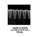
- FIG. 2 ais a representation illustrating the conformal deposition of GST film with a Ge:Sb:Te composition close to 4:1:5.
- FIG. 2 bis an X-ray diffraction scan pattern of a GST film with a Ge:Sb:Te composition close to 4:1:5 and showing amorphous characteristics.
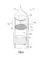
- FIG. 3is a schematic representation of another GST deposition process that can be used to form chalcogenide materials of the present disclosure.
- FIG. 4is a schematic representation of another GST deposition process that can be used to form chalcogenide materials of the present disclosure.
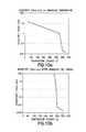
- FIG. 5is a graphical representation of growth rate of a GST composition versus the inverse of the activation region temperature.
- FIG. 6is a graphical representation of growth rate of a GST composition versus the inverse of the activation region temperature.
- FIG. 7is a schematic representation of a phase change memory cell device including chalcogenide material of the present disclosure.
- FIG. 8 ais a representation illustrating the conformal deposition of GST film with a Ge:Sb:Te composition close to 2:2:5.
- FIG. 8 bis an X-ray diffraction scan pattern of a GST film with a Ge:Sb:Te composition close to 2:2:5 showing some crystalline characteristics.
- FIG. 9is a graphical representation illustrating GST film having C and N.
- FIG. 10 ais a graphical representation of the resistivity of GST film after annealing.
- FIG. 10 bis a graphical representation of the resistivity of GST film after annealing.
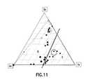
- FIG. 11is a compositional phase diagram reflecting relative amounts of germanium (Ge), antimony (Sb) and tellurium (Te) in GST films, showing a compositional region A for highly conformal MOCVD characterized by high tellurium content, as distinguished from region B reflecting lower tellurium content films.
- FIG. 12is an enlarged view of region A of FIG. 11 , showing data points associated with photomicrographs showing good morphology in high tellurium content films.
- FIG. 13is a graph of resistance, in ohms, as a function of reset current, in milliamps, showing data for a physical vapor deposition of 225 composition GST, and data for MOCVD of corresponding GST. The data show a low reset current to be achieved by conformal chemical vapor deposition in the low temperature process of the present disclosure.
- FIG. 14is a graph of reset current, in milliamps, as a function of voltage, in volts, for a physical vapor deposition of 225 composition GST, and data for MOCVD of corresponding GST.
- the datalike that in FIG. 13 , show a low reset current to be achieved by conformal chemical vapor deposition in the low temperature process of the present disclosure.
- FIG. 15is a graph of resistivity, as a function of temperature in degree C., for a GST film containing the following atomic percentages: 32% germanium, 13% antimony and 54% tellurium. The film had a thickness of 140 ⁇ . Rho(RT) was approximately 6 ohm-centimeters to 0.03 ohm-centimeter. The film was not fully annealed (255° C.). The graph shows a crystallization temperature on the order of 220° C.
- FIG. 16is a graph of atomic concentrations of germanium, antimony, tellurium, and nitrogen, and Si intensity (arbitrary units), as a function of depth, in nanometers for an illustrative GST film having a nitrogen impurity at a concentration of less than 10 atomic percent.
- FIG. 17 ais a graph of atomic concentration of oxygen and nitrogen, and Ge, Te, and Sb intensity (arbitary units), as a function of depth, in nanometers, for an illustrative GST film having essentially oxygen-free character and a carbon impurity on the order of approximately 3%.
- FIG. 17 bis a graph of atomic concentration of oxygen and carbon, and Ge, Te, and Sb intensity (arbitary units), as a function of depth, in nanometers, for an illustrative GST film having essentially oxygen-free character and a carbon impurity on the order of approximately 10%.
- FIG. 18is a photomicrograph showing GST material as deposited at low temperature in a low aspect ratio structure, in contact with a TiAlN bottom layer and a TiN top layer, after 7 ⁇ 10 9 phase change cycles.
- FIG. 19is a photomicrograph of GST deposited in a high aspect ratio structure of a virgin device.
- FIG. 20is a photomicrograph of a PVD GST film after chemical mechanical planarization (CMP).
- FIG. 21shows the Reset Current (R-I) curves for PCM devices made from MOCVD GST 325, MOCVD GST 225, and PVD GST 225 with N and C.
- FIG. 22is a graph of I-V curves in PCM devices, for PVD GST 225, MOCVD GST 225, and MOCVD GST 325.
- FIG. 23is a graph of resistance as a function of set pulse width and set pulse fall time, for (a) set-speed using a square-shaped pulse method, and (b) set-speed using a set-sweep pulse method.
- FIG. 24is a graph of time versus 1/KT, showing the 10 year data retention temperature established using the time to fail method.
- FIG. 25is a graph of cycle endurance test data for a PCM device made of MOCVD GST325, using a square pulse method with a reset pulse time of 100 ns and set pulse time of 500 ns with a cycle period of 1 ⁇ sec.
- CVDis defined as the deposition of a solid on a surface from a chemical precursor, and includes but is not limited to the following: Atmospheric pressure CVD (APCVD), Low pressure CVD (LPCVD), Ultrahigh vacuum CVD (UHVCVD), Aerosol-assisted CVD (AACVD), Digital CVD (DCVD), Direct liquid injection CVD (DLICVD), Microwave plasma-assisted CVD (MPCVD), Plasma-enhanced CVD (PECVD), Remote plasma-enhanced CVD (RPECVD), Atomic layer CVD (ALCVD), Hot wire CVD (HWCVD), Metalorganic chemical vapor deposition (MOCVD), Hybrid physical-chemical vapor deposition (HPCVD), Rapid thermal CVD (RTCVD), and Vapor phase epitaxy (VPE).
- APCVDAtmospheric pressure CVD
- LPCVDLow pressure CVD
- UHVCVDUltrahigh vacuum CVD
- AACVDAerosol-
- the present disclosurerelates in a primary aspect to chalcogenide materials having utility for manufacture of semiconductor materials, devices and device precursor structures.
- the chalcogenide materialscan for example include those selected from the group consisting of:
- the material of the above-described typecan include material in which Ge x Sb y Te z therein has an atomic composition selected from the group consisting of:
- GST materials of the present disclosurescan be doped, e.g., with carbon and/or nitrogen.
- the materialis doped with carbon at 2 to 20 at. %, or at 3 to 20 at. %, or at 2 to 15 at. %, or at 2 to 10 at. %, or at 3 to 10 at. %, or at 2 to 6 at. %.
- the materialcan be doped with nitrogen at 2 to 20 at. %, or at 3 to 20 at. %, or at 3 to 15 at. %, or at 3 to 12 at. %, or at 3 to 10 at. %, or at 5 to 10 at. %.
- the specific dopant levelscan be readily determined within the skill of the art, based on the present disclosure, by conducting doping at varying levels and characterizing the resulting films as to their characteristics and performance qualities.
- the GST materials of the present disclosurecan be conformally coated on substrates, e.g., microelectronic device or device precursor structure substrates, to form microelectronic devices including such material.
- substratese.g., microelectronic device or device precursor structure substrates
- the microelectronic devicecan include a phase change memory cell, or a memory device.
- One highly advantageous GST film composition for such purposecomprises from 0 to 50% Sb, from 50 to 80% Te, from 20 to 50% Ge, from 3 to 20% N and from 2 to 15% carbon, and wherein all atomic percentages of all components of the film total to 100 atomic %.
- Another advantageous GST film composition useful for the foregoing applicationscomprises from 10 to 50% Sb, from 50 to 80% Te, from 10 to 50% Ge, from 3 to 20% N and from 3 to 20% carbon, and wherein all atomic percentages of all components of the film total to 100 atomic %.
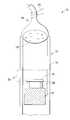
- FIG. 1depicts a system for producing and depositing low temperature GST materials is generally designated by the reference number 10 and hereinafter referred to as “system 10 .”
- system 10GST materials comprising reactants are deposited onto a substrate (hereinafter referred to as “wafer”) as a film to form a phase change material (PCM) device.
- wafera substrate
- PCMphase change material
- the system 10comprises a deposition chamber 12 or furnace defined by at least one wall 14 .
- the inner surface of the wall of the deposition chamber 12defines a heat shield 14 .
- An inlet 16is located in the deposition chamber 12 to allow for the introduction of the reactants (e.g., precursors, co-reactants, and inert materials such as carriers) into the system 10 .
- the inlet 16is located in communication with any suitable source, such as a ProEvap® carrier gas operating system (ATMI, Inc., Danbury, Conn., USA), from which the reactants are delivered.
- a showerhead 18is located downstream of the inlet 16 to facilitate the efficient dispersal and delivery of the reactants delivered from the source.
- the present inventionis not limited to the use of a showerhead, however, as other similar devices are within the scope of this disclosure.
- a heating coil 20 or any other suitable heating devicemay be located at the inlet 16 to heat the reactants during delivery thereof from the source.
- the reactantsmay be pre-cracking compositions, pre-reaction compositions, partial decomposition products, and/or other materials that are suitable for controllably altering reaction conditions in the deposition chamber to produce the desired film.
- exemplary reactantsinclude, but are not limited to, germanium n-butylamidinate (germanium precursor), tris(dimethylamido)antimony (antimony precursor), and diterbutyltelluride (tellurium precursor).
- a heating stage 24is located in the deposition chamber 12 .
- the heating stage 24can be heated using any suitable source of energy to cause heat to radiate therefrom.
- the heating stage 24may be heated using an electric current.
- the present inventionis not so limited, however, as the heating stage 24 can be heated using other means.
- the heating stage 24comprises one or more support pins 28 that extend therethrough, each support pins being configured to support a wafer 30 on which the GST materials are deposited.
- Any suitable number of support pins 28can be used to support the wafer 30 .
- three support pins 28 arranged in a triangular patterncan be used.
- the present inventionis not limited to any particular number of support pins 28 or any particular arrangement thereof, as any number and arrangement of support pins is within the scope of the present disclosure.
- the areas of contact between the support pins 28 and the wafer 30are minimal.
- the support pins 28may be fixed relative to the heating stage 24 , or they may be extendable therethrough. In embodiments in which the support pins 28 are extendable through the heating stage, the wafer 30 may be elevated or lowered as desired.
- a gas including one or more of Ge, Sb, and Te precursors and optionally one or more co-reactant gasesare delivered into the deposition chamber 12 from the source via inlet 16 .
- the wafer 30is located at a distance of about 5 mm from the heating stage 24 and is, therefore, radiantly heated. Heat radiated from the heating stage 24 also heats the heat shield 14 .
- the precursorsare activated in an activation region 38 of the deposition chamber 12 .
- the temperature of the heating stage 24is about 320 degrees C. to about 400 degrees C.
- the temperature of the wafer 30is about 160 degrees C. to about 240 degrees C.
- the temperature of the heat shield 14 in the activation region 38 above wafer 40has a temperature that is higher than that of the wafer.
- the temperature of the heating stage 24is maintained such that the temperature of the activation region 38 is about 100 degrees C. higher than that of the wafer 30 .
- the activation region 38may be located anywhere in the deposition chamber 12 such that the source materials are activated, location of the activation region on the surface of the wafer means that the deposition of GST film is substantially a surface reaction.
- the present inventionis not so limited, however, as there may be a gas phase reaction of source material prior to deposition on the wafer 30 . However, any such gas phase reaction should be minimized.
- the pressure in the deposition chamber 12is about 1 Torr to about 10 Torr, and preferably about 2.5 Torr.
- the present inventionis not limited in this regard, however, as other pressures may be maintained in the deposition chamber 12 without departing from the broader aspects of the processes and apparatuses disclosed herein.
- FIG. 1As is shown in FIG. 1 , by supporting the wafer 30 using the support pins 28 , the temperature to which the wafer is subjected is reduced (relative to the heating stage 24 ). As a result, a composition of GST having a Te content greater than 50% by increasing the influx of Te precursors without leading to the formation of crystalline GST films has been achieved, as shown in FIG. 2 a .
- FIG. 2 ban X-ray diffraction pattern is shown for a similar GST composition. Table 1 below shows examples of many such films. Using this process, GST can be obtained with a Ge:Sb:Te ratio of 4:1:5, 2:2:5, or the like.
- the wafer 30may be elevated by the support pins 28 and located thereon such that the device side of the wafer faces the heating stage 24 .
- the device side of the wafer 30is heated by thermal radiation to a temperature of about 180 degrees C. to about 240 degrees C. by the heating stage 24 , which is at a temperature of about 340 degrees C. to about 420 degrees C.
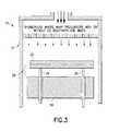
- a system for producing and depositing low temperature GST materialsis generally designated by the reference number 110 and hereinafter referred to as “system 110 .”
- GST materialsare again deposited onto a wafer 30 to form a PCM device.
- a deposition chamber 112is defined by at least one wall 114 , the inner surface of which defines a heat shield.
- An inlet 116is located in the deposition chamber 112 to allow for the introduction of precursors, co-reactants, and inert materials.
- the inlet 116is located in communication with any suitable source, such as a ProEvap® carrier gas operating system from which the precursors and/or other materials are delivered.
- a showerhead 118 or similar deviceis located between the inlet 116 and the wall 114 of the deposition chamber 112 to facilitate the efficient dispersal and delivery of the precursors and/or other materials delivered from the source.
- a screen 122is located downstream of the showerhead 118 .
- the screen 122may be a copper mesh that is operably associated with a heating mean 120 to distribute heat at a substantially uniform temperature throughout the cross-sectional area of the path through which the precursors and co-reactants flow.
- the present inventionis not limited in this regard, however, as other materials may comprise the screen.
- the volume between the showerhead 118 and the screen 122defines an activation region 138 , which includes the heating means 120 .
- the deposition chamber 112includes a heating stage 124 located therein.
- the heating stage 124can be heated using any suitable source of energy.
- the wafer 30is located on the heating stage 124 .
- a source gas including the precursors and optionally one or more co-reactant gasesare delivered into the deposition chamber 112 via inlet 116 .
- the source gasis heated via the heating means 120 , thereby activating the precursors before being deposited on the wafer 30 .
- the heated source gaspasses through the screen 122 , the heated source gas is substantially uniformly and evenly dispersed.
- the reactioncan be carried out at wafer temperatures as low as 150 degrees C. and activation region temperatures as low as 200 degrees C. Raising the wafer temperature to 200 degrees C. while the activation zone temperature is 200 degrees C. can also lead to the film formation.
- a wafer temperature of 200 degrees C.alone will not provide the film properties and beneficial characteristics that are most desirable for GST film formation, particularly for the desired high Te GST formation.
- the growth (in terms of thickness measured in Angstroms) of the film deposited on the wafer 30is plotted versus the reciprocal of temperature for a GST composition having the ratios of 30:15:55.
- the growth ratedecreases as the temperature in the activation region is decreased from 270 degrees C. to 240 degrees C. when the wafer is maintained at 150 degrees C.
- FIG. 6when the wafer 30 is 200 degrees C., a similar growth rate decrease is observed, thereby indicating that lower activation region temperatures lead to lower amounts of Te deposited.
- each precursor and co-reactantcan be activated separately at different temperatures to maximize the efficiency of the deposition of the film.
- the separate activationmay further avoid the over activation of less stable precursors and thus avoid resulting in undesirable precursor by products or the premature consumption of the precursors by deposition (such as the formation of particles via gas phase reaction).
- one or more components of the source gasmay be added downstream of the activation region 138 .
- the Te and Sb precursors and co-reactantsare passed through the activation region 138 with the germanium precursor (GeM) being added downstream of the activation region 138 .
- the temperature of the germanium precursorcan be controlled independently of the temperatures of other precursors and/or co-reactants, and a deposition process can be obtained in which the temperature of the wafer 30 can be about 110 degrees C. and the temperature in the activation region 138 can be as low as about 186 degrees C., as shown in Table 3.
- FIG. 7is a schematic representation of a phase change memory cell device 200 including chalcogenide material of the present disclosure as phase change memory elements 202 and 204 .
- the cell deviceincludes bit line and word line elements, and includes phase change memory element 202 in a polycrystalline state, and the phase change memory element 204 in an amorphous state.
- phase change material of the present disclosurecan be provided in thin film and other conformations, and can be utilized in a variety of microelectronic device applications.
- the precursorsare activated together with co-reactants by being heated, thereby providing for increased reactivity in the activation regions.
- the passage of the precursors and co-reactants along the length of the activation regionspartly determines the degree of reactivity of the precursors.
- the heating element(s)can be located inside the heating stages of the deposition chambers, or they can be located in the showerhead upstream of the substrate, upstream of the showerhead and downstream of the inlet, or even further upstream in the inlet through which the precursors and co-reactants are introduced. Multiple heating sources can be used for achieving uniform thermal activations of precursors.
- the Ge, Sb, and Te precursor vaporscan be used with or without co-reactants such as ammonia gas, hydrogen, nitrogen, or other suitable gases.
- a gas flow ratecan be about 20 to about 200 standard cubic centimeter per minute (sccm), particularly for a one inch size substrate (wafer coupon). Gas flow rates are scaled up accordingly for larger size substrates (e.g., 300 mm or 8 inch wafers).
- ammonium gas at 200 sccmcan be diluted to 50 sccm using a hydrogen flow at 150 sccm to decrease the growth rate or to promote conformal fill benefits.
- Reduced process pressure from 2.5 Torr to lower valuesmay also improve chemical mass transfer functions and provide for better uniformity and improved conformal deposition.
- higher pressures at 10 Torrcan improve the growth rate due to higher molecular concentrations from the precursors being available.
- Diluent gasessuch as Ar, N 2 , He, and combinations thereof can also be introduced from a bubbler or a ProEvap carrier gas operating system.
- dopantssuch as N, C, In, Sn, Se, and combinations of the foregoing can be added to the GST film to produce a film having the formula Ge x Sb y Te z A m , wherein A is the dopant element and wherein x is about 0.1-0.6, y is about 0-0.7, z is about 0.2-0.9, and m is about 0-0.15.
- FIG. 8 aa scanning electron micrograph depiction of a GST film having a nitrogen dopant illustrates substantially conformal deposition deep into vias having high aspect ratios. The thickness of the film was 385.4 Angstroms, and the composition included 14.1% Ge, 26.4% Sb, 52.6% Te and 6.97% N.
- an X-ray diffraction scan pattern of an as-grown filmillustrates that the film is conformal and amorphous.
- XRDX-ray diffraction
- FIG. 9a Secondary Ion Mass Spectroscope (SIMS) scan of a GST film shows the Ge, Sb, Te, and N content distribution.
- SIMSSecondary Ion Mass Spectroscope
- both carbon and nitrogen dopingcan co-exist in a GST film.
- carbon dopingmay reduce the reset current of the GST film, and nitrogen doping may improve conformality of the film. It is estimated that carbon doping reduces the reset current by 2-3 times.
- the wafer 30may be subjected to an annealing process to reduce nitrogen content if it is deemed desirable to reduce the content of nitrogen at this stage.
- Table 4below lists the experimental results.
- the nitrogen content of the films after annealingare substantially reduced in relation to the nitrogen content of the as-deposited films. It will be correspondingly appreciated that the content of nitrogen, carbon and other film components is to be understood in the context of the description herein as referring to the film content after annealing and/or other post-deposition processing, unless otherwise expressly stated.
- the systems and processes of the present disclosurecan be implemented with activation of one or more precursors in the inlet of the deposition chamber.
- pre-activation of one or more of the precursorsmay be carried out in a pre-activation zone that is outside the deposition chamber, e.g., a separate pre-activation chamber that may for example be arranged in series or other flow arrangements with respect to the deposition chamber.
- a separate pre-activation chamberthat may for example be arranged in series or other flow arrangements with respect to the deposition chamber.
- Such dedicated pre-activation chambercan in many instances be more closely controlled as to its temperature, in relation to activation heating within the deposition chamber.
- the precursorcan be activated in a dedicated activation chamber, e.g., a supply vessel in which the precursor is activated, at the time of dispensing for use.
- the pre-activation chamberis desirably operated at substantially higher temperature than inside the chamber, in order to minimize susceptibility to particle formation.
- Pre-activationis typically used for one more precursors that are typically only partially decomposed at high temperature.
- the Ge, Sb and Te precursorsmay be passed into the deposition chamber without pre-activation, but such pre-activation may be employed to make one or more of such precursors more effective in low temperature deposition.
- multiple showerheadsmay be employed.
- to showerheadsmay be utilized, one for pre-activated precursor(s) and another for non-pre-activated precursor(s).
- the two showerheadsmay be interlaced with one another and arranged to uniformly distribute both the pre-activated precursor and non-pre-activated precursor over the entire wafer surface.
- Such multiple showerhead arrangementspermit concurrent feeding of activated and non-activated precursors to the deposition chamber to enable low process temperature to be utilized for GST film formation.
- a tellurium precursorcan be activated by heating in an inlet passage to the deposition chamber, or alternatively in a dedicated activation chamber in which the requisite heating occurs to activate the precursor.
- the antimony and germanium precursorswould not be activated, but would be introduced with the activated tellurium precursor to the deposition portion of the deposition chamber.
- both tellurium and antimony precursorsmay be activated and the germanium may be passed into the deposition chamber without any activation prior to entering the deposition portion of the deposition chamber.
- Processes of the present disclosureenable deposition of conformal high tellurium content GST films.
- Specific precursorsare particularly beneficial in achieving such high tellurium content.
- di-tertiary-butyl tellurium, (tBu) 2 Tecan be activated to form di-tertiary-butyl ditellurium, tBu-Te—Te-tBu, as a stable thermal decomposition product.
- Such tellurium precursor tBu-Te—Te-tBuis advantageously utilized for GST film formation with a germanium precursor such as Ge[Pr i NC(n-Bu)NPr i ] 2 , denoted as “GeM” for ease of notation.
- such precursor tBu-Te—Te-tBucan be used for low temperature deposition of tellurium-containing films, including GST films as well as BiTe 3 films and cadmium telluride (CdTe) films.
- CVD conformalitycan be enhanced utilizing such tellurium precursor.
- CVD conformalitycan be enhanced through use of low deposition temperatures, chemical modification of the precursor chemistry and modification of the CVD process parameters.
- the use of (tBu) 2 Teresults in higher tellurium concentrations in the product film when higher temperature zones are used to induce pre-reaction of the precursor. Such higher temperature zones can be in close proximity to the wafer surface, but are separate and distinct regions within the CVD deposition system.
- partial pyrolytic decomposition of (tBu) 2 Te to form tBu-Te—Te-tBuhigher tellurium content films are achievable at lower substrate temperatures. Since incorporation of tellurium can have large effects on the electrical and thermal behavior of GST films, the ability to increase tellurium content of deposited films is highly advantageous.
- ditelluride precursorsof the form R—Te—Te—R, wherein each R is independently selected from methyl, ethyl, isopropyl, tertiary butyl and trimethylsilyl, is advantageous in producing high tellurium content films, in CVD, ALD, digital CVD and other vapor deposition processes, optionally including activation of such precursor in the deposition chamber or at the inlet to or even outside (upstream from) such chamber, be on the thermal activation occurring at the wafer surface in the deposition process.
- Such precursorscan be used for forming GST films as well as other tellurium-containing films such as CdTe photovoltaic films and thermoelectric thin films based on II-VI telluride materials.
- Co-reactantsmay be utilized with such ditelluride precursors, including, for example, inert gases, reducing gases (hydrogen, ammonia, diborane, silane, etc.), and the like.
- ditelluride precursors discussed abovecan be synthesized from the reaction of Cl—Te—Te—Cl with either RLi or Gringard reagents, wherein R is the same as previously described.
- FIG. 11is a compositional phase diagram reflecting relative amounts of germanium (Ge), antimony (Sb) and tellurium (Te) in GST films, showing a compositional region A for highly conformal MOCVD characterized by high tellurium content, as distinguished from region B reflecting lower tellurium content films.
- region Ashows data points associated with high tellurium content (>50 at. % Te) conformal MOCVD GST films, achievable by low temperature MOCVD processes of the present disclosure.
- the circled datumrefers to a germanium-antimony-telluride composition containing from about 20 to about 25 atomic percent germanium, from about 20 to 25 atomic percent antimony, and from about 50 to 60 atomic percent of tellurium, e.g., 22.5 at. % germanium, 22.5 at. % antimony and 55 at. % tellurium, sometimes herein referred to as the “225 composition.”
- FIG. 12is an enlarged view of region A of FIG. 11 , showing data points associated with photomicrographs evidencing good morphology in high tellurium content films, and identifying the 225 composition by the number “225”.
- the present disclosurecontemplates a vapor deposition process for depositing a GeTe-containing film on a substrate, comprising vaporizing a germanium-containing precursor and a tellurium-containing precursor to form a precursor vapor, contacting the germanium-containing precursor vapor with a substrate at a temperature that is below 250° C., and depositing on the substrate a conformal germanium-containing film.
- Such processmay further comprise tellurium in the conformal germanium-containing film.
- the conformal filmmay be substantially amorphous.
- the germanium precursormay include a germanium alkyl amidinate.
- germanium precursorsthat may be usefully employed in forming germanium-containing films include Ge(IV) amides, Ge(IV) mixed alkyl/amide, Ge(II) amidinate, Ge(II) amide, Ge(IV) guanidinate, germylene, and Ge(II)Cp, wherein Cp is cyclopentadienyl.
- the tellurium precursormay comprise a di-alkyl tellurium precursor.
- the substrate in the foregoing processmay have temperature of from about 110° C. to about 250° C. In such process, the substrate temperature is desirably below the crystallization temperature of the multi-component germanium-containing film.
- the low temperature MOCVD GST deposition process of the present disclosurehas been determined to yield product GST films with equal to or better properties than those achievable by physical vapor deposition processes involving trench deposition of GST.
- Table 5Set out below in Table 5 is a tabulation comparing performance of a physical vapor deposition (CVD) film deposited with a GST 225 composition containing containing 22.5% germanium, 22.5% antimony and 55% tellurium against CVD Composition A in which the film was deposited by chemical vapor deposition utilizing a low temperature process in accordance with the present invention, and a film noted below as “Best of CVD” based on a film deposited at using a precursor mixture including di-t-butyl telluride precursor, GeM (germanium n-butyl amidinate) germanium precursor and tris(dimethylamido)antimony precursor.
- CVDphysical vapor deposition
- the Composition A filmcontained approximately 30% germanium, 20% antimony and 50% tellurium.
- the “Best of CVD”was based on an average of films of three different film compositions, including a first film composition containing approximately 30% germanium, 20% antimony and 50% tellurium, a second film composition containing 22.5% germanium, 22.5% antimony and 55% tellurium, and a third film composition containing from 40 to 45% germanium, from 5 to 10% antimony and from 50 to 55% tellurium.
- the germanium-containing filmcan have the composition Ge x Sb y Te z A m , wherein A is a dopant element selected from the group of N, C, In, Sn, and Se, and wherein x is from 0.1 to 0.6, y is from 0 to 0.7, z is from 0.2 to 0.9, and m is from 0 to 0.15. In various embodiments in which antimony is present, y can be from 0.1 to 0.7. In various embodiments in which the germanium-containing film is doped, m can be from 0.01 to 0.15.
- the vapor deposition processitself may be of any suitable type, and may comprise chemical vapor deposition (CVD).
- the substratemay be disposed in a CVD chamber.
- the CVD chambermay be constructed and arranged in any suitable manner.
- the CVD chamberincludes an activation region having a first heat source.
- the vapor deposition processmay be carried out in which at least one precursor of the germanium-containing film is activated by the first heat source.
- the processmay further involve heating the substrate using a second heat source.
- germanium-rich GST filmsdoping can be carried out to improve compositional and performance properties of the film.
- Germaniumcan be doped in the GST film at levels of for example 5 to 10 atomic percent.
- the 225 composition, containing 22.5% germanium, 22.5% antimony and 55% telluriumcan be composition enhanced to contain from 27.5 to 32.5% germanium, with tellurium still being as high as 55%, or between 50 and 55%, with the remainder being antimony.
- germaniumwill increase crystallization temperature of the resulting alloy compared with that of the 225 composition, due to germanium doping imparting “friction” to atomic movement, and germanium's tetravalent coordinating bonding structure to tellurium being more stable than that of antimony bonding to tellurium.
- the ratio of GeTe to Sb 2 Te 3can be changed to alter crystallization temperature and other aspects of the materials properties of the film.
- GSTis actually a pseudo-alloy, typically being a mix of the true alloy GeTe and Sb 2 Te 3 .
- the 225 composition GST film materialis a mixture of two portions of GeTe and one portion of Sb 2 Te 3 .
- Germanium dopingcan be employed to increase germanium content above that of the 2:1 ratio of GeTe to Sb 2 Te 3 .
- the resulting alloywill reduce the tellurium content from 55% to a somewhat lower level around 50% or even slightly less, depending on the specific ratio of GeTe to Sb 2 Te 3 .
- a 3:1 ratio of GeTe to Sb 2 Te 3will be atomically Ge 3 Sb 2 Te 6 , which as the atomic percentage of 27.2% germanium, 18.2% antimony and 54.5% tellurium
- a 4:1 ratio of GeTe to Sb 2 Te 3will be atomically 30.7% germanium, 15.4% antimony, and 53.9% tellurium
- a 5:1 ratio of GeTe to Sb 2 Te 3will be 33.3% germanium, 13.3% antimony and 53.3% tellurium
- a 6:1 ratio of GeTe to Sb 2 Te 3will be 35.3% germanium, 11.8% antimony and 52.9% tellurium
- a 10:1 ratio of GeTe to Sb 2 Te 3will be 40% germanium, 8% antimony and 52% tellurium.
- Germanium-rich GST or germanium-doped 225 GSTmay have a ratio of GeTe:Sb 2 Te 3 that is in a range of from 3:1 to 10:1.
- compositionsinclude a composition containing 27.2% germanium, 18.2% antimony and 54.5% tellurium as a first example, a composition containing 40% germanium, 8% antimony and 52% tellurium as a second example, a composition containing 30% germanium, 19% antimony and 51% tellurium as a third example, a composition containing 30% germanium, 16% antimony and 54% tellurium as a fourth example, and a composition containing 32% germanium, 14% antimony and 54% tellurium as a fifth example.
- germanium-rich GST or germanium self-doped 225 GSTprovides superior film properties, and includes GST alloys having from 27 to 33% germanium, from 14 to 23% antimony and from 50 to 55% tellurium.
- GST films with dopants other than Ge, Sb or Teare contemplated by the present disclosure. Any suitable dopant species may be employed that improve the properties of the GST film for its intended purpose.
- the GST filmsmay be doped with carbon and/or nitrogen to improve film properties, e.g., to significantly reduce reset current of the film in a phase change memory applications.
- nitrogen doping at atomic percentages of from 4 to 10% and carbon doping at atomic percentages of from 2 to 6%can be employed.
- the present disclosurecontemplates conformal GST thin films having an atomic composition comprising from 10 to 50% Sb, from 50 to 80% Te, from 10 to 50% Ge, from 0 to 20% N (e.g., from 3 to 20% N) and from 0 to 20% carbon (e.g., from 3 to 20% N), and wherein all atomic percentages of all components of the film total to 100 atomic %.
- Such filmsmay be formed using CVD, e.g., in a low temperature CVD process as described herein.
- Additional illustrative GST film compositionsinclude compositions in which ratios of germanium (Ge) to antimony (Sb) to tellurium (Te) (atomic % (at. %)) may be about 2:2:5, about 4:1:5, about 30:15:55, or the like.
- Gegermanium
- Sbantimony
- Tetellurium
- the ratiois 2:2:5
- Geis about 20-25 at. %
- Sbis about 20-25 at. %
- Teis about 50-60 at. %.
- the ratiois 4:1:5
- Geis about 40-45 at. %
- Sbis about 5-10 at. %
- Teis about 50-55 at. %.
- Geis about 27-33 at.
- a further illustrative GST film compositioncontains from about 25 to 35% germanium, from about 15 225% antimony, and from about 45 to 55% tellurium. Another illustrative GST film composition contains from about 35 to 45% germanium, from about 1 to 10% antimony, and from about 45 to 55% tellurium. A still further illustrative film composition contains from about 75% to about 85% germanium, from about 5 to about 15% antimony, and from about 5 to about 15% tellurium. Another illustrative GST film composition contains from 27 to 33% germanium, from 45 to 55% tellurium, and the balance being antimony. In general, it is possible to add carbon up to 10 atomic percent, e.g., 3%, and to add nitrogen up to 15 atomic percent, e.g., 5%.
- FIG. 23is a photomicrograph of a void-free fill of GST in a via structure.
- FIG. 13is a graph of resistance, in ohms, as a function of reset current, in milliamps, showing data for a physical vapor deposition of 225 composition GST, and data for MOCVD of corresponding GST. The data show a low reset current to be achieved by conformal chemical vapor deposition in the low temperature process of the present disclosure.
- FIG. 14is a graph of reset current, in milliamps, as a function of voltage, in volts, for a physical vapor deposition of 225 composition GST, and data for MOCVD of corresponding GST.
- the datalike that in FIG. 13 , show a low reset current to be achieved by conformal chemical vapor deposition in the low temperature process of the present disclosure.
- FIG. 15is a graph of resistance, in amperes, as a function of temperature in degree C. for a GST film containing the following atomic percentages: 32% germanium, 13% antimony and 54% tellurium. The film had a thickness of 140 ⁇ . Rho(RT) was approximately 6 ohm-centimeters to 0.03 ohm-centimeter. The film was not fully annealed (255° C.). The graph shows a crystallization temperature on the order of 220° C.
- FIG. 16is a graph of atomic concentrations of germanium, antimony, tellurium, and nitrogen, and Si intensity (arbitrary units), as a function of depth, in nanometers for an illustrative GST film having a nitrogen impurity at a concentration of less than 10 atomic percent.
- FIG. 17 ais a graph of atomic concentration of oxygen and nitrogen, and Ge, Te, and Sb intensity (arbitary units), as a function of depth, in nanometers, for an illustrative GST film having essentially oxygen-free character and a carbon impurity on the order of approximately 3%.
- FIG. 17 bis a graph of atomic concentration of oxygen and carbon, and Ge, Te, and Sb intensity (arbitary units), as a function of depth, in nanometers, for an illustrative GST film having essentially oxygen-free character and a carbon impurity on the order of approximately 10%.
- FIG. 18is a photomicrograph showing GST material as deposited at low temperature in a low aspect ratio structure, in contact with a TiAlN bottom layer and a TiN top layer, after 7 ⁇ 10 9 phase change cycles.
- FIG. 19is a photomicrograph of GST deposited in a high aspect ratio structure of a virgin device.
- the deposition of GST films utilizing a low temperature chemical vapor deposition process as described in the present disclosurecan be carried out to form a phase change memory device by steps including forming a bottom electrode for the device, followed by etching the bottom electrode/heater inside a via to form a recessed via. GST material then is deposited in the via, followed by chemical mechanical planarization, and cleaning of the device structure, following which a top electrode structure is formed.
- deposition of the GST materials using heatfacilitates the reactivity of the Ge, Sb, and Te by increasing the reactivity thereof.
- Such an increase in reactivitymeans that GST can be deposited on a substrate at a lower temperature (e.g., at about 110 degrees C. to 250 degrees C.), yet achieving high percentages of Te.
- the processcan be a batch process in which any number of substrates can be processed in a similar configuration just by simply duplicating the process for additional substrates.
- FIG. 10 ais a graph of resistivity, measured in ohm-cm, as a function of temperature, in ° C., for a GST film of 2:2:5 Ge:Sb:Te having a thickeness of 444.1 Angstroms, with a film composition of 20.5% Ge, 23.5% Sb and 56.0% Te.
- FIG. 10 ais a graph of resistivity, measured in ohm-cm, as a function of temperature, in ° C., for a GST film of 2:2:5 Ge:Sb:Te having a thickeness of 444.1 Angstroms, with a film composition of 20.5% Ge, 23.5% Sb and 56.0% Te.
- 10 bis a corresponding graph for a GST film having a composition of 4:0.5:5 Ge:Sb:Te, with a thickness of 308.1 Angstroms, and composed of 44.8% Ge, 5.3% Sb, and 49.8% Te. Also, as is shown in Table 4, the nitrogen content of a GST film is markedly reduced after annealing.
- the composition of MOCVD GST deposited in the test deviceswas 30% Ge, 20% Sb, and 50% Te with an estimated composition range accuracy of +/ ⁇ 3%.
- dopants of N and Cwere incorporated from precursors and co-reactants at atomic concentrations of 7% and 4% respectively as measured by SIMS (secondary ion mass spectrometry), with an estimated accuracy of +/ ⁇ 4% for N and +/ ⁇ 2% for C.
- the as-deposited filmwas amorphous, smooth, and conformal, so a high aspect ratio 3:1 device structure was able to be filled. Typical film density is equivalent between the as-grown film and annealed films.
- the doping in this MOCVD GST 325also increased the crystallization temperature, Tx, to 220° C.
- FIG. 18shows the device structure containing a bottom TiAlN electrode as a heater, filled GST in the pore, and a Top TiN electrode.
- the shallow porewas formed by etching a hole with sloped side-walls in 500 ⁇ PECVD SiO 2 , etch stopped on TiAlN.
- the test structureshad nominal design dimensions ranging from 70 nm to 200 nm.
- the TiAlN surface inside the porewas cleaned using a dilute HF (50:1) dip prior to MOCVD deposition of 750 ⁇ GST. A 620 ⁇ Ti/TiN layer was then deposited over the GST for the top electrode.
- the Ti/TiN and GSTwere patterned by lithography and a dry etch to isolate the GST and TiN top electrode in a single PCM device for testing.
- the test device in this discussionhad a 100 nm nominal pore size based on FIB-SEM measurements.
- FIG. 21shows the Reset-Current (R-I) curves for PCM devices made from MOCVD GST325, MOCVD GST 225, and PVD GST225 without N and C. All the devices have a nominal size of 100 nm and measured sized of 103 nm for MOCVD GST325 and 106 nm for MOCVD GST225 and PVD GST225. In the device made with MOCVD GST325, the set resistance was below 10 k ⁇ and the reset resistance more than 1 M ⁇ , demonstrating more than 100 ⁇ in dynamic range, as shown in FIG. 21 .
- the reset current in the device using MOCVD GST325was 0.6 mA, which was more than 2 ⁇ smaller than the 1.4 mA reset current for a device made from PVD GST225. A reduction of reset current permitted more devices to be programmed in parallel, increasing the write bandwidth, a critical aspect for PCM in DRAM and SCM applications.
- FIG. 22is a graph of I-V curves in PCM devices, for PVD GST 225, MOCVD GST 225, and MOCVD GST 325.
- MOCVD GST225achieved an equivalent low reset current level at similar N and C doping ranges, the set resistance for MOCVD GST325 was more than 2 ⁇ lower than that of MOCVD GST225, making it an attractive alloy composition as an alternative to MOCVD GST225.
- FIG. 23shows set-speed measurements for a MOCVD GST325 device with a 100 nm pore diameter.
- Set-speed characterization measured by the square shaped pulse methodis shown in curve (a), and curve (b) displays set-speed characterization by the set sweep pulse method.
- the devicewas first reset with a reset current pulse at 120% of the saturation reset current level as indicated by the horizontal lines with open symbols.
- the reset pulse durationwas always 100 ns.
- Amplitude of the square shaped set pulsewas approximately half of the reset amplitude and varied in duration from 1 ins to 3 ⁇ s.
- the set sweep pulsehad a maximum amplitude of 120% reset level, with a rise of 100 ns, a width of 200 ns and a varying fall times ranging from 50 ns to 2 ⁇ s.
- the set speedwas determined by the time required for the resistance level to fall below the demarcation level which is 1 ⁇ 6 th logarithmically up from full set between the full reset and full set levels.
- FIG. 24shows the 10 year data retention temperature established using the time to fail method. The time to fail is measured after a resistance value of a fully reset device reaches a 67 k ⁇ demarcation level at elevated temperatures of 180, 185, 190, and 200° C.
- FIG. 24shows the fail-time data extrapolated to 10 years on an Arrhenius plot, giving a temperature of 102° C. with an estimated error margin of +/ ⁇ 10° C. The estimated activation energy was calculated as 2.2 eV
- the 10 year data retention temperature of a PVD GST225 devicewas measured to be 105° C.
- the CVD GST325 alloy with N and C dopinghad a similar 10 year data retention temperature to that of a PVD GST225 device.
- FIG. 25shows the cycle endurance test for a PCM device made of MOCVD GST325.
- the testused the square pulse method with a reset pulse time of 100 ns and set pulse time of 500 ns with a cycle period of 1 ⁇ sec.
- 1.3 ⁇ 10 9 cycleswere completed with a stable Rreset, Rset, Vt, Vh, and dV/dI before the device degraded, resulting in a reduced dynamic range.
- the device shown in FIG. 18endured more than 7 ⁇ 10 9 cycles without failure or void formation under similar test conditions in this non-confined low aspect ratio structure.
- One of the keys for the high cycle endurancewas the deposit of void-free and high density amorphous film, which maintained a small density change in the crystalline phase after annealing without void formation.
- ALD vapor deposition processthat is used to deposit the GST material can be carried out in any suitable manner to produce product GST films, within the skill of the art, based on the disclosure herein.
- ALD process parameterse.g., pulse times, cycle durations, temperatures, pressures, volumetric flow rates, etc. can be determined by simple successive empirical runs in which process parameters are selectively varied to determine the best multivariable process envelope for conducting the ALD vapor deposition process.
- the chemical species employed to deposit the chalcogenide materialmay be thermally activated or in other manner energized to generate transitory species for the deposition.
- a chemical speciesmay be transformed into a different chemical form to provide deposition species that may for example be short-lived but are sufficiently present to enable deposition, in the transport from the activation region to the wafer surface.
- a deposition chemical speciesmay be generated in situ for the deposition operation.
- the carbon and nitrogen species that are incorporated in the GST film in various embodiments of the disclosuremay be provided in a bound or non-bound form.
- the nitrogen as mentionedmay be introduced in free form as nitrogen gas, or alternatively as a nitrogen-containing moiety in a precursor or coreactant that is introduced to the deposition operation.
- nucleation sites present in the filmmay derive from the presence of carbon as well as nitrogen, and may also be generated as a result of carbon-nitrogen interaction.
- the more nucleation sites present in the chalcogenide filmthe faster nucleation will take place and the more rapid will be the transformation between amorphous and crystalline states in the operation of the GST material.
- the greater the population of nucleation sitesthe shorter are the required crystalline lengths involved in the propagation of crystalline transformation, and the quicker the GST device will be in response to a phase change stimulus.
- germanium-antimony-tellurium (GST) alloy films of the disclosureare usefully employed in phase change memory devices, including NOR flash memory, dynamic random access memory (DRAM) and storage class memory (SCM), taking advantage of the properties of such chalcogenide alloy, which can be readily switched between crystalline (binary 1) and amorphous (binary 0) states, or in some applications, between amorphous, crystalline and two additional partially crystalline states.
- phase change memory devicesincluding NOR flash memory, dynamic random access memory (DRAM) and storage class memory (SCM)
Landscapes
- Chemical & Material Sciences (AREA)
- Organic Chemistry (AREA)
- Inorganic Chemistry (AREA)
- Engineering & Computer Science (AREA)
- Materials Engineering (AREA)
- Mechanical Engineering (AREA)
- Metallurgy (AREA)
- General Chemical & Material Sciences (AREA)
- Chemical Kinetics & Catalysis (AREA)
- Manufacturing & Machinery (AREA)
- Crystallography & Structural Chemistry (AREA)
- Chemical Vapour Deposition (AREA)
Abstract
Description
- (i) material of the formula GexSbyTezCmNn
- wherein:
- x is about 0.1-0.6, y is about 0-0.7, z is about 0.2-0.9, m is about 0.02-0.20, and n is about 0.2-0.20;
- (ii) material of the formula GexSbyTezAm, wherein A is a dopant element selected from the group of N, C, In, Sn, and Se, and wherein x is from 0.1 to 0.6, y is from 0 to 0.7, z is from 0.2 to 0.9, and m is from 0 to 0.15;
- (iii) material containing 27.5 to 33% germanium, with tellurium up to 55%, and the remainder being antimony;
- (iv) 225 GeSbTe doped with germanium to yield germanium-rich GeSbTe material;
- (v) germanium-enriched GeSbTe having a ratio of GeTe:Sb2Te3that is in a range of from 3:1 to 10:1;
- (vi) GeSbTe material containing 25 to 60% germanium, 8 to 25% antimony, and 40 to 55% tellurium; and
- (vii) material selected from the group consisting of materials (ii)-(vi), as doped with at least one of carbon and nitrogen, wherein the amount of each is in a range of from 2 to 20%.
- (i) material of the formula GexSbyTezCmNn
- wherein:
- x is about 0.1-0.6, y is about 0-0.7, z is about 0.2-0.9, m is about 0.02-0.20, and n is about 0.02-0.20;
- (ii) material of the formula GexSbyTezAm, wherein A is a dopant element selected from the group of N, C, In, Sn, and Se, and wherein x is from 0.1 to 0.6, y is from 0 to 0.7, z is from 0.2 to 0.9, and m is from 0 to 0.15;
- (iii) material containing 27.5 to 33% germanium, with tellurium up to 55%, and the remainder being antimony;
- (iv) 225 GeSbTe doped with germanium to yield germanium-rich GeSbTe material;
- (v) germanium-enriched GeSbTe having a ratio of GeTe:Sb2Te3that is in a range of from 3:1 to 10:1;
- (vi) GeSbTe material containing 25 to 60% germanium, 8 to 25% antimony, and 40 to 55% tellurium; and
- (vii) material selected from the group consisting of materials (ii)-(vi), as doped with at least one of carbon and nitrogen, wherein the amount of each is in a range of from 2 to 20%.
- (i) 22.5 at. % germanium, 22.5 at. % antimony and 55 at. % tellurium;
- (ii) 27.5 to 32.5 at. % germanium and from 50 to 55 at. % tellurium;
- (iii) 27 to 33% germanium, from 14 to 23% antimony and from 50 to 55% tellurium;
- (iv) 27.2% germanium, 18.2% antimony and 54.5% tellurium;
- (v) 30.7% germanium, 15.4% antimony, and 53.9% tellurium;
- (vi) 33.3% germanium, 13.3% antimony and 53.3% tellurium;
- (vii) 35.3% germanium, 11.8% antimony and 52.9% tellurium;
- (viii) 36% germanium, 14% antimony and 50% tellurium;
- (ix) 40% germanium, 8% antimony and 52% tellurium;
- (x) 40% germanium, 5% antimony and 55% tellurium;
- (xi) 30% germanium, 19% antimony and 51% tellurium;
- (xii) 30% germanium, 16% antimony and 54% tellurium; and
- (xiii) 32% germanium, 14% antimony and 54% tellurium.
| TABLE 1 |
| GST films with varying heating source |
| temperatures and wafer temperatures. |
| Thick- | Heating Stage | Wafer | ||||
| ness | temperature | temperature | ||||
| (nm) | Ge % | Sb % | Te % | N % | (degrees C.) | (degrees C.) |
| 12.9 | 25.4 | 30.9 | 43.9 | not | 322 | 160 |
| measured | ||||||
| 7.5 | 39.4 | 16.9 | 43.7 | not | 342 | 180 |
| measured | ||||||
| 33.8 | 18 | 30.9 | 51.2 | not | 342 | 180 |
| measured | ||||||
| 42.6 | 14.5 | 29.1 | 56.3 | 0 | 362 | 197 |
| 41.6 | 31.3 | 12.4 | 52.2 | 4.1 | 362 | 197 |
| 36.6 | 30.6 | 14.8 | 49.3 | 5.33 | 362 | 197 |
| 16 | 45.3 | 5.09 | 49.7 | not | 362 | 197 |
| measured | ||||||
| 27 | 32.7 | 14.9 | 48.9 | 3.46 | 382 | 220 |
| 35 | 23 | 24 | 53 | 0 | 402 | 240 |
| 39 | 20 | 25 | 55 | 0 | 402 | 240 |
| 13.3 | 35.6 | 10.3 | 54.1 | not | 402 | 240 |
| measured | ||||||
| 195 | 9 | 0.8 | 84 | 5.4 | 402 | 240 |
| TABLE 2 |
| Process Results based on configuration of FIG. 4 |
| Activation | ||||||
| Thick- | region | Wafer | ||||
| Experimental | ness | temperature | temperature | |||
| Run # | (A) | Ge % | Sb % | Te % | (degrees C.) | (degrees C.) |
| #3031 | 101.8 | 24.7 | 22.3 | 53 | 220 | 150 |
| #3032 | 67 | 29.6 | 11.2 | 67 | 220 | 150 |
| #3033 | 42.7 | 35 | 9.4 | 55.8 | 220 | 150 |
| #3034 | 57 | 30.1 | 28.5 | 41.4 | 220 | 130 |
| #3035 | 79.7 | 18 | 31.7 | 50.3 | 200 | 200 |
| #3036 | 58.8 | 30.1 | 28 | 58.8 | 220 | 150 |
| TABLE 3 |
| Deposition results with internal GeM source |
| Activation region | Wafer | |||||
| Thick- | temperature | temperature | ||||
| Run | Ge % | Sb % | Te % | ness | (degrees C.) | (degrees C.) |
| 3031 | 24.7 | 22.3 | 53.0 | 101.8 | 220 (heating coil 0.5 | 150 |
| in. above wafer) | ||||||
| 3032 | 29.6 | 11.2 | 59.2 | 67 | 220 | 150 |
| 3033 | 35.0 | 9.25 | 55.8 | 42.7 | 220 | 130 |
| 3034 | 30.1 | 28.5 | 41.4 | 56.6 | 186 | 125 |
| 3035 | 18.0 | 31.7 | 50.3 | 79.7 | 200 | 200 |
| 3036 | 30.1 | 28.0 | 41.9 | 58.8 | 186 | 110 |
| TABLE 4 | ||
| Composition of | Composition of | |
| GST as-deposited | GST post 45 min | |
| Experiment # | ||
| 1 | 413.9A, 35.4% Ge, | 45.9% Ge, 4.5% Sb, |
| 3.6% Sb, 45.7% Te, | 47.1% Te 2.43% N after 350 C. | |
| 15.27% N | 45 min | |
| Experiment # | ||
| 2 | 396.9A, 43.9% Ge, | 368.3A, 44.3% Ge, 5.2% Sb, |
| 4.88% Sb, 51.2% Te | 49.6% Te, 0.91% N after | |
| 11% N measured | 350 C. 45 min annealing | |
| Experiment # | ||
| 3 | 355.3A, 36.2% Ge, | 296.0A, 44.2% Ge, 6.6% Sb, |
| 5.0% Sb, 42.4% Te, | 49.1% Te, 0.08% N after | |
| 16.31 | 350 C. 45 min annealing | |
| TABLE 5 | ||||
| PVD GST | 225 | CVD Comp A | Best of CVD | |
| Void free fill at | <1:1 | >3:1 down to | >5:1 down to | |
| 35 | 40 nm | |||
| Irst@ 70 nm | 0.8 mA | 0.5~1.0 mA | 0.2 | |
| 10 Year | 105° C. | 102° C. | 125° C. | |
| Retention, | 2.2 eV | 3.4 eV | ||
| crystallization | ||||
| Set speed | ||||
| 200 ns | 260 ns | <50 ns | ||
| ‘85% to 50% | ||||
| fail’-11 ns | ||||
| full fail time-30 ns | ||||
| Cycle | >1 × 10⁹ | >7 × 10⁹ | >1 × 10¹⁰ | |
| Endurance | ||||
| Drift coefficient | 0.1 | 0.1 | 0.1 | |
Claims (21)
Priority Applications (1)
| Application Number | Priority Date | Filing Date | Title |
|---|---|---|---|
| US13/637,018US9012876B2 (en) | 2010-03-26 | 2010-05-21 | Germanium antimony telluride materials and devices incorporating same |
Applications Claiming Priority (3)
| Application Number | Priority Date | Filing Date | Title |
|---|---|---|---|
| US31782910P | 2010-03-26 | 2010-03-26 | |
| US13/637,018US9012876B2 (en) | 2010-03-26 | 2010-05-21 | Germanium antimony telluride materials and devices incorporating same |
| PCT/US2010/035854WO2011119175A1 (en) | 2010-03-26 | 2010-05-21 | Germanium antimony telluride materials and devices incorporating same |
Publications (2)
| Publication Number | Publication Date |
|---|---|
| US20130078475A1 US20130078475A1 (en) | 2013-03-28 |
| US9012876B2true US9012876B2 (en) | 2015-04-21 |
Family
ID=44673506
Family Applications (1)
| Application Number | Title | Priority Date | Filing Date |
|---|---|---|---|
| US13/637,018Active2030-12-31US9012876B2 (en) | 2010-03-26 | 2010-05-21 | Germanium antimony telluride materials and devices incorporating same |
Country Status (4)
| Country | Link |
|---|---|
| US (1) | US9012876B2 (en) |
| KR (1) | KR101706809B1 (en) |
| TW (1) | TW201132787A (en) |
| WO (1) | WO2011119175A1 (en) |
Cited By (4)
| Publication number | Priority date | Publication date | Assignee | Title |
|---|---|---|---|---|
| US20130112933A1 (en)* | 2010-05-21 | 2013-05-09 | Advanced Technology Materials, Inc. | Germanium antimony telluride materials and devices incorporating same |
| US9640757B2 (en) | 2012-10-30 | 2017-05-02 | Entegris, Inc. | Double self-aligned phase change memory device structure |
| US10186552B2 (en) | 2016-07-28 | 2019-01-22 | Samsung Electronics Co., Ltd. | Variable resistance memory device and method of manufacturing the same |
| TWI662605B (en)* | 2015-06-16 | 2019-06-11 | 荷蘭商Asm Ip控股公司 | Method of forming structure or gate stack on substrate surface |
Families Citing this family (13)
| Publication number | Priority date | Publication date | Assignee | Title |
|---|---|---|---|---|
| CN102352488B (en) | 2006-11-02 | 2016-04-06 | 诚实公司 | The antimony useful for the CVD/ALD of metallic film and germanium complexes |
| US20090215225A1 (en) | 2008-02-24 | 2009-08-27 | Advanced Technology Materials, Inc. | Tellurium compounds useful for deposition of tellurium containing materials |
| US9054295B2 (en)* | 2011-08-23 | 2015-06-09 | Micron Technology, Inc. | Phase change memory cells including nitrogenated carbon materials, methods of forming the same, and phase change memory devices including nitrogenated carbon materials |
| KR102077641B1 (en)* | 2013-08-06 | 2020-02-14 | 삼성전자주식회사 | Phase-change material layer and method of manufacturing the same |
| JP6210544B2 (en)* | 2013-10-22 | 2017-10-11 | 気相成長株式会社 | Te agent and M-Te film forming method |
| US20160181515A1 (en)* | 2014-12-18 | 2016-06-23 | Stmicroelectronics S.R.I. | Embedded phase change memory devices and related methods |
| KR102304301B1 (en)* | 2014-12-23 | 2021-09-23 | 삼성전자주식회사 | Resistance-change material layer and phase-change memory device including the same |
| KR101952729B1 (en)* | 2016-04-29 | 2019-02-27 | 세종대학교산학협력단 | Preparing method of chalcogen-containing film using atomic layer deposition |
| US10808316B2 (en)* | 2018-05-10 | 2020-10-20 | International Business Machines Corporation | Composition control of chemical vapor deposition nitrogen doped germanium antimony tellurium |
| US12004434B2 (en) | 2020-11-02 | 2024-06-04 | International Business Machines Corporation | Fill-in confined cell PCM devices |
| WO2024001426A1 (en)* | 2022-06-30 | 2024-01-04 | 华中科技大学 | Phase-change thin film, thin film preparation method, and phase-change memory |
| IT202300009990A1 (en)* | 2023-05-17 | 2024-11-17 | St Microelectronics Int Nv | PHASE CHANGE MEMORY ELEMENT PARTICULARLY SUITABLE FOR EMBEDDED AND AUTOMOTIVE APPLICATIONS |
| CN116789451B (en)* | 2023-06-06 | 2024-10-29 | 先导薄膜材料(广东)有限公司 | Silicon-germanium-antimony-tellurium doped target material and preparation method thereof |
Citations (169)
| Publication number | Priority date | Publication date | Assignee | Title |
|---|---|---|---|---|
| US3467686A (en) | 1967-10-03 | 1969-09-16 | Union Carbide Corp | Preparation of organosilicon-nitrogen compounds |
| JPS5838296A (en) | 1981-08-31 | 1983-03-05 | Ichiro Kijima | Novel antimony compound |
| US4383119A (en) | 1982-06-04 | 1983-05-10 | Chemplex Company | Organomagnesium compounds |
| US4491669A (en) | 1980-11-12 | 1985-01-01 | Petrarch Systems Inc. | Mixed alkoxyaminosilanes, methods of making same and vulcanizing silicons prepared therefrom |
| US4499198A (en) | 1982-10-07 | 1985-02-12 | Chemplex Company | Polymerization catalysts and methods |
| US4895709A (en) | 1985-04-26 | 1990-01-23 | Sri International | Method of preparing metal carbides, nitrides, and the like |
| US4927670A (en) | 1988-06-22 | 1990-05-22 | Georgia Tech Research Corporation | Chemical vapor deposition of mixed metal oxide coatings |
| US4948623A (en) | 1987-06-30 | 1990-08-14 | International Business Machines Corporation | Method of chemical vapor deposition of copper, silver, and gold using a cyclopentadienyl/metal complex |
| US4960916A (en) | 1989-09-29 | 1990-10-02 | United States Of America As Represented By The Secretary Of The Navy | Organometallic antimony compounds useful in chemical vapor deposition processes |
| US4962214A (en) | 1988-05-11 | 1990-10-09 | Massachusettes Institute Of Technology | Catalytic enantioselective addition of hydrocarbon equivalents to alpha, beta-unsaturated carbonyl compounds |
| US5003092A (en) | 1989-06-02 | 1991-03-26 | The Research Foundation Of State University Of Ny | Use of R2 MR' to prepare semiconductor and ceramic precursors |
| US5008422A (en) | 1985-04-26 | 1991-04-16 | Sri International | Polysilazanes and related compositions, processes and uses |
| US5084588A (en) | 1990-07-05 | 1992-01-28 | Union Carbide Chemicals & Plastics Technology Corporation | Reducing halide contamination in alkoxy silanes |
| US5139825A (en) | 1989-11-30 | 1992-08-18 | President And Fellows Of Harvard College | Process for chemical vapor deposition of transition metal nitrides |
| US5178911A (en) | 1989-11-30 | 1993-01-12 | The President And Fellows Of Harvard College | Process for chemical vapor deposition of main group metal nitrides |
| US5210254A (en) | 1992-03-31 | 1993-05-11 | Union Carbide Chemicals & Plastics Technology Corporation | Acidic halide neutralization in alkoxysilanes |
| US5225561A (en) | 1990-07-06 | 1993-07-06 | Advanced Technology Materials, Inc. | Source reagent compounds for MOCVD of refractory films containing group IIA elements |
| JPH05311423A (en) | 1992-05-12 | 1993-11-22 | Dowa Mining Co Ltd | Production of sputtering target |
| US5268496A (en) | 1992-05-27 | 1993-12-07 | Wacker-Chemie Gmbh | Process for the preparation of polysilazanes |
| JPH0680413A (en) | 1992-08-27 | 1994-03-22 | Toshiro Maruyama | Method for chemical vapor growth of silicon dioxide film |
| US5312983A (en) | 1991-02-15 | 1994-05-17 | Advanced Technology Materials, Inc. | Organometallic tellurium compounds useful in chemical vapor deposition processes |
| JPH06293778A (en) | 1993-04-05 | 1994-10-21 | Idemitsu Kosan Co Ltd | Silanamine derivative and its production |
| US5417823A (en) | 1993-12-17 | 1995-05-23 | Ford Motor Company | Metal-nitrides prepared by photolytic/pyrolytic decomposition of metal-amides |
| US5442200A (en) | 1994-06-03 | 1995-08-15 | Advanced Technology Materials, Inc. | Low resistance, stable ohmic contacts to silcon carbide, and method of making the same |
| US5453494A (en) | 1990-07-06 | 1995-09-26 | Advanced Technology Materials, Inc. | Metal complex source reagents for MOCVD |
| JPH07263431A (en) | 1994-03-17 | 1995-10-13 | Sony Corp | Formation of tantalum-containing high dielectric film |
| JPH0874055A (en) | 1994-07-07 | 1996-03-19 | Mitsubishi Materials Corp | Formation of high purity silver film |
| US5566045A (en) | 1994-08-01 | 1996-10-15 | Texas Instruments, Inc. | High-dielectric-constant material electrodes comprising thin platinum layers |
| US5583205A (en) | 1993-11-12 | 1996-12-10 | Florida State University | Metalorganic chemical vapor deposition method for depositing f-series metal or nitrogen and metal amides for use in mocvd |
| US5596522A (en) | 1991-01-18 | 1997-01-21 | Energy Conversion Devices, Inc. | Homogeneous compositions of microcrystalline semiconductor material, semiconductor devices and directly overwritable memory elements fabricated therefrom, and arrays fabricated from the memory elements |
| US5653806A (en) | 1995-03-10 | 1997-08-05 | Advanced Technology Materials, Inc. | Showerhead-type discharge assembly for delivery of source reagent vapor to a substrate, and CVD process utilizing same |
| US5687112A (en)* | 1996-04-19 | 1997-11-11 | Energy Conversion Devices, Inc. | Multibit single cell memory element having tapered contact |
| US5698726A (en) | 1995-05-04 | 1997-12-16 | Huels Aktiengesellschaft | Process for preparing amino-functional organosilanes low in or free of chloro-functional organosilanes |
| US5719417A (en) | 1996-11-27 | 1998-02-17 | Advanced Technology Materials, Inc. | Ferroelectric integrated circuit structure |
| US5820664A (en) | 1990-07-06 | 1998-10-13 | Advanced Technology Materials, Inc. | Precursor compositions for chemical vapor deposition, and ligand exchange resistant metal-organic precursor solutions comprising same |
| US5919522A (en) | 1995-03-31 | 1999-07-06 | Advanced Technology Materials, Inc. | Growth of BaSrTiO3 using polyamine-based precursors |
| US5976991A (en) | 1998-06-11 | 1999-11-02 | Air Products And Chemicals, Inc. | Deposition of silicon dioxide and silicon oxynitride using bis(tertiarybutylamino) silane |
| US6005127A (en) | 1997-11-24 | 1999-12-21 | Advanced Technology Materials, Inc. | Antimony/Lewis base adducts for Sb-ion implantation and formation of antimonide films |
| US6015917A (en) | 1998-01-23 | 2000-01-18 | Advanced Technology Materials, Inc. | Tantalum amide precursors for deposition of tantalum nitride on a substrate |
| WO2000015865A1 (en) | 1998-09-11 | 2000-03-23 | Asm Microchemistry Oy | Method for growing oxide thin films containing barium and strontium |
| US6086779A (en) | 1999-03-01 | 2000-07-11 | Mcgean-Rohco, Inc. | Copper etching compositions and method for etching copper |
| US6133051A (en) | 1998-06-30 | 2000-10-17 | Advanced Technology Materials, Inc. | Amorphously deposited metal oxide ceramic films |
| WO2000067300A1 (en) | 1999-04-29 | 2000-11-09 | President And Fellows Of Harvard College | Liquid precursors for formation of materials containing alkali metals |
| US6146608A (en) | 1997-11-24 | 2000-11-14 | Advanced Technology Materials, Inc. | Stable hydride source compositions for manufacture of semiconductor devices and structures |
| JP2001067720A (en) | 1999-08-31 | 2001-03-16 | Toray Ind Inc | Optical recording medium |
| US6269979B1 (en) | 1999-10-05 | 2001-08-07 | Charles Dumont | Multi-compartmented mixing dispenser |
| US6281022B1 (en) | 1999-04-28 | 2001-08-28 | Sharp Laboratories Of America, Inc. | Multi-phase lead germanate film deposition method |
| US20020004266A1 (en) | 2000-06-01 | 2002-01-10 | Kazuhiko Hashimoto | Apparatus and method for forming thin film at low temperature and high deposition rate |
| US6399208B1 (en) | 1999-10-07 | 2002-06-04 | Advanced Technology Materials Inc. | Source reagent composition and method for chemical vapor deposition formation or ZR/HF silicate gate dielectric thin films |
| US20020090815A1 (en) | 2000-10-31 | 2002-07-11 | Atsushi Koike | Method for forming a deposited film by plasma chemical vapor deposition |
| JP2002220658A (en) | 2001-01-26 | 2002-08-09 | Ricoh Co Ltd | Sputtering target for optical disk and its manufacturing method |
| US6506666B2 (en) | 2000-05-15 | 2003-01-14 | Micron Technology, Inc. | Method of fabricating an SrRuO3 film |
| US6511718B1 (en) | 1997-07-14 | 2003-01-28 | Symetrix Corporation | Method and apparatus for fabrication of thin films by chemical vapor deposition |
| US20030135061A1 (en) | 2000-04-03 | 2003-07-17 | Norman John Anthony Thomas | Volatile precursors for deposition of metals and metal-containing films |
| US6646122B1 (en) | 2000-02-29 | 2003-11-11 | Unilever Home & Personal Care Usa, Division Of Conopco, Inc. | Ligand and complex for catalytically bleaching a substrate |
| US20040012009A1 (en) | 2002-02-20 | 2004-01-22 | Stmicroelectronics S.R.L. | Sublithographic contact structure, phase change memory cell with optimized heater shape, and manufacturing method thereof |
| US20040038808A1 (en) | 1998-08-27 | 2004-02-26 | Hampden-Smith Mark J. | Method of producing membrane electrode assemblies for use in proton exchange membrane and direct methanol fuel cells |
| US6716271B1 (en) | 2002-10-29 | 2004-04-06 | Advanced Technology Materials, Inc. | Apparatus and method for inhibiting decomposition of germane |
| WO2004046417A2 (en) | 2002-11-15 | 2004-06-03 | President And Fellows Of Harvard College | Atomic layer deposition using metal amidinates |
| US6750079B2 (en) | 1999-03-25 | 2004-06-15 | Ovonyx, Inc. | Method for making programmable resistance memory element |
| US6767830B2 (en) | 2002-08-07 | 2004-07-27 | Advanced Technology Materials, Inc. | Br2SbCH3 a solid source ion implant and CVD precursor |
| KR20040076225A (en) | 2003-02-24 | 2004-08-31 | 삼성전자주식회사 | Phase change memory device and method for fabricating the same |
| US6787186B1 (en) | 1997-12-18 | 2004-09-07 | Advanced Technology Materials, Inc. | Method of controlled chemical vapor deposition of a metal oxide ceramic layer |
| WO2004076712A1 (en) | 2003-02-26 | 2004-09-10 | Saes Getters S.P.A. | Bismuth precursor solution for use in a cvd process and deposition process of a bismuth containing thin film using thereof |
| US20040197945A1 (en) | 2003-04-05 | 2004-10-07 | Rohm And Haas Electronic Materials L.L.C. | Germanium compounds |
| EP1466918A1 (en) | 2003-04-08 | 2004-10-13 | Tosoh Corporation | Novel bismuth compounds, process of producing the same, and process of producing a film |
| US20040215030A1 (en) | 2003-04-22 | 2004-10-28 | Norman John Anthony Thomas | Precursors for metal containing films |
| US20050029502A1 (en) | 2003-08-04 | 2005-02-10 | Hudgens Stephen J. | Processing phase change material to improve programming speed |
| US6861559B2 (en) | 2002-12-10 | 2005-03-01 | Board Of Trustees Of Michigan State University | Iminoamines and preparation thereof |
| US6869638B2 (en) | 2001-03-30 | 2005-03-22 | Advanced Tehnology Materials, Inc. | Source reagent compositions for CVD formation of gate dielectric thin films using amide precursors and method of using same |
| US6872963B2 (en) | 2002-08-08 | 2005-03-29 | Ovonyx, Inc. | Programmable resistance memory element with layered memory material |
| US20050082624A1 (en) | 2003-10-20 | 2005-04-21 | Evgeni Gousev | Germanate gate dielectrics for semiconductor devices |
| KR20050048891A (en) | 2003-11-20 | 2005-05-25 | 주식회사 에버테크 | Universal thin film deposit device |
| WO2005084231A2 (en) | 2004-02-27 | 2005-09-15 | Asm Aemrica, Inc. | Germanium deposition |
| US20050208699A1 (en) | 2004-03-18 | 2005-09-22 | International Business Machines Corporation | Phase Change Memory Cell On Silicon-On Insulator Substrate |
| US20050267345A1 (en) | 2001-07-02 | 2005-12-01 | The University Of Texas System, Board Of Regents | Applications of light-emitting nanoparticles |
| US20050283012A1 (en) | 2004-06-16 | 2005-12-22 | Chongying Xu | Copper (I) compounds useful as deposition precursors of copper thin films |
| US20050287747A1 (en) | 2004-06-29 | 2005-12-29 | International Business Machines Corporation | Doped nitride film, doped oxide film and other doped films |
| US6984591B1 (en) | 2000-04-20 | 2006-01-10 | International Business Machines Corporation | Precursor source mixtures |
| US20060006449A1 (en) | 2004-07-06 | 2006-01-12 | Jeong Yong-Kuk | Semiconductor integrated circuit devices having a hybrid dielectric layer and methods of fabricating the same |
| WO2006012052A2 (en) | 2004-06-25 | 2006-02-02 | Arkema, Inc. | Amidinate ligand containing chemical vapor deposition precursors |
| US20060027451A1 (en) | 2004-08-06 | 2006-02-09 | Park Jeong-Hee | Methods for sputtering a target material by intermittently applying a voltage thereto and related apparatus, and methods of fabricating a phase-changeable memory device employing the same |
| US6998289B2 (en) | 2001-08-31 | 2006-02-14 | Intel Corporation | Multiple layer phase-change memory |
| US20060035462A1 (en) | 2004-08-13 | 2006-02-16 | Micron Technology, Inc. | Systems and methods for forming metal-containing layers using vapor deposition processes |
| US7005303B2 (en) | 1997-11-20 | 2006-02-28 | Advanced Technology Materials, Inc. | Low temperature chemical vapor deposition process for forming bismuth-containing ceramic thin films useful in ferroelectric memory devices |
| US20060046521A1 (en) | 2004-09-01 | 2006-03-02 | Vaartstra Brian A | Deposition methods using heteroleptic precursors |
| US20060049447A1 (en) | 2004-09-08 | 2006-03-09 | Lee Jung-Hyun | Antimony precursor, phase-change memory device using the antimony precursor, and method of manufacturing the phase-change memory device |
| US7029978B2 (en) | 2003-08-04 | 2006-04-18 | Intel Corporation | Controlling the location of conduction breakdown in phase change memories |
| JP2006124262A (en) | 2004-11-01 | 2006-05-18 | Dainippon Printing Co Ltd | InSb nanoparticles |
| KR100585175B1 (en) | 2005-01-31 | 2006-05-30 | 삼성전자주식회사 | Method for manufacturing thin film thin film by chemical vapor deposition |
| US20060115595A1 (en) | 2004-10-05 | 2006-06-01 | Rohm And Haas Electronic Materials Llc | Organometallic compounds |
| EP1675194A2 (en) | 2004-12-27 | 2006-06-28 | Samsung Electronics Co., Ltd. | GE precursor, GST thin layer, phase-change memory device |
| US20060141710A1 (en) | 2004-12-27 | 2006-06-29 | Jae-Man Yoon | NOR-type flash memory device of twin bit cell structure and method of fabricating the same |
| US20060172067A1 (en) | 2005-01-28 | 2006-08-03 | Energy Conversion Devices, Inc | Chemical vapor deposition of chalcogenide materials |
| US7087482B2 (en) | 2001-01-19 | 2006-08-08 | Samsung Electronics Co., Ltd. | Method of forming material using atomic layer deposition and method of forming capacitor of semiconductor device using the same |
| US20060180811A1 (en) | 2005-02-14 | 2006-08-17 | Samsung Electronics Co., Ltd. | Precursor, thin layer prepared including the precursor, method of preparing the thin layer and phase-change memory device |
| US7114517B2 (en) | 2001-11-26 | 2006-10-03 | Sund Wesley E | High purity fluid delivery system |
| KR20070025612A (en) | 2005-09-03 | 2007-03-08 | 삼성전자주식회사 | Formation method of phase change material layer, manufacturing method of phase change memory unit and phase change memory device using same |
| KR100695168B1 (en) | 2006-01-10 | 2007-03-14 | 삼성전자주식회사 | Formation method of phase change material thin film, manufacturing method of phase change memory device using same |
| US20070090336A1 (en) | 2005-07-08 | 2007-04-26 | Elpida Memory, Inc | Semiconductor memory |
| US20070121363A1 (en) | 2005-11-28 | 2007-05-31 | Macronix International Co., Ltd. | Phase Change Memory Cell and Manufacturing Method |
| WO2007070218A2 (en) | 2005-08-09 | 2007-06-21 | Ovonyx, Inc. | Chalcogenide devices and materials having reduced germanium or telluruim content |
| US20070154637A1 (en) | 2005-12-19 | 2007-07-05 | Rohm And Haas Electronic Materials Llc | Organometallic composition |
| US20070246748A1 (en) | 2006-04-25 | 2007-10-25 | Breitwisch Matthew J | Phase change memory cell with limited switchable volume |
| KR20070105752A (en) | 2006-04-27 | 2007-10-31 | 재단법인서울대학교산학협력재단 | Phase change memory cell and manufacturing method thereof |
| WO2007126690A2 (en) | 2006-04-04 | 2007-11-08 | Micron Technology, Inc. | Phase change memory elements using self- aligned phase change material layers and methods of making and using same |
| WO2007140813A1 (en) | 2006-06-02 | 2007-12-13 | L'air Liquide Societe Anonyme Pour L'etude Et L'exploitation Des Procedes Georges Claude | Method of forming high-k dielectric films based on novel titanium, zirconium, and hafnium precursors and their use for semiconductor manufacturing |
| US7312165B2 (en) | 2004-05-05 | 2007-12-25 | Jursich Gregory M | Codeposition of hafnium-germanium oxides on substrates used in or for semiconductor devices |
| US20080003359A1 (en) | 2006-06-28 | 2008-01-03 | President And Fellows Of Harvard College | Metal (IV) tetra-amidinate compounds and their use in vapor deposition |
| WO2008002546A1 (en) | 2006-06-28 | 2008-01-03 | President And Fellows Of Harvard College | Metal(iv) tetra-amidinate compounds and their use in vapor deposition |
| US20080035906A1 (en) | 2006-07-13 | 2008-02-14 | Samsung Electronics Co., Ltd. | Germanium compound, semiconductor device fabricated using the same, and methods of forming the same |
| US20080035961A1 (en) | 2006-08-14 | 2008-02-14 | Industrial Technology Research Institute | Phase-change memory and fabrication method thereof |
| US20080078984A1 (en) | 2006-09-29 | 2008-04-03 | Samsung Electronics Co., Ltd. | Semiconductor device and method of fabricating the same |
| US20080099791A1 (en)* | 2006-10-04 | 2008-05-01 | Macronix International Co., Ltd. | Memory Cell Device with Circumferentially-Extending Memory Element |
| WO2008057616A2 (en) | 2006-11-02 | 2008-05-15 | Advanced Technology Materials, Inc. | Antimony and germanium complexes useful for cvd/ald of metal thin films |
| US20080118636A1 (en) | 2006-11-21 | 2008-05-22 | Samsung Electronics Co., Ltd | Method of forming phase change layer using a germanium precursor and method of manufacturing phase change memory device using the same |
| KR20080052362A (en) | 2006-12-05 | 2008-06-11 | 한국전자통신연구원 | Modem performance analysis device and method, and function test method of modem performance analysis device |
| US7397060B2 (en) | 2005-11-14 | 2008-07-08 | Macronix International Co., Ltd. | Pipe shaped phase change memory |
| US7399666B2 (en) | 2005-02-15 | 2008-07-15 | Micron Technology, Inc. | Atomic layer deposition of Zr3N4/ZrO2 films as gate dielectrics |
| US7402851B2 (en) | 2003-02-24 | 2008-07-22 | Samsung Electronics Co., Ltd. | Phase changeable memory devices including nitrogen and/or silicon and methods for fabricating the same |
| US7419698B2 (en) | 2001-10-26 | 2008-09-02 | Sigma-Aldrich Co. | Precursors for chemical vapor deposition |
| KR20080080273A (en) | 2005-12-12 | 2008-09-03 | 오보닉스, 아이엔씨. | Chalcogenide devices and materials with reduced low maenyum or tellurium content |
| US20080210163A1 (en) | 2006-11-21 | 2008-09-04 | David Keith Carlson | Independent Radiant Gas Preheating for Precursor Disassociation Control and Gas Reaction Kinetics in Low Temperature CVD Systems |
| US7425735B2 (en) | 2003-02-24 | 2008-09-16 | Samsung Electronics Co., Ltd. | Multi-layer phase-changeable memory devices |
| US20080254232A1 (en) | 2007-04-09 | 2008-10-16 | President And Fellows Of Harvard College | Cobalt nitride layers for copper interconnects and methods for forming them |
| US20080254218A1 (en) | 2007-04-16 | 2008-10-16 | Air Products And Chemicals, Inc. | Metal Precursor Solutions For Chemical Vapor Deposition |
| JP2008252088A (en) | 2007-03-09 | 2008-10-16 | Commiss Energ Atom | Multi-level data memorisation device with phase change material |
| US20080290335A1 (en) | 2007-05-21 | 2008-11-27 | Industrial Technology Research Institute | Phase change memory device and method for fabricating the same |
| WO2009006272A1 (en) | 2007-06-28 | 2009-01-08 | Advanced Technology Materials, Inc. | Precursors for silicon dioxide gap fill |
| US20090020738A1 (en) | 2007-07-20 | 2009-01-22 | Thomas Happ | Integrated circuit including force-filled resistivity changing material |
| KR20090008799A (en) | 2007-07-19 | 2009-01-22 | 주식회사 아이피에스 | Thin film deposition apparatus, thin film deposition method and gap-fill method of semiconductor device |
| US7488967B2 (en) | 2005-04-06 | 2009-02-10 | International Business Machines Corporation | Structure for confining the switching current in phase memory (PCM) cells |
| WO2009020888A1 (en) | 2007-08-08 | 2009-02-12 | Advanced Technology Materials, Inc. | Strontium and barium precursors for use in chemical vapor deposition, atomic layer deposition and rapid vapor deposition |
| US20090075420A1 (en) | 2007-09-18 | 2009-03-19 | Samsung Electronics Co., Ltd. | Method of forming chalcogenide layer including te and method of fabricating phase-change memory device |
| WO2009034775A1 (en) | 2007-09-13 | 2009-03-19 | Nippon Mining & Metals Co., Ltd. | Method for producing sintered body, sintered body, sputtering target composed of the sintered body, and sputtering target-backing plate assembly |
| US20090087561A1 (en) | 2007-09-28 | 2009-04-02 | Advanced Technology Materials, Inc. | Metal and metalloid silylamides, ketimates, tetraalkylguanidinates and dianionic guanidinates useful for cvd/ald of thin films |
| KR20090036771A (en) | 2007-10-10 | 2009-04-15 | 삼성전자주식회사 | Method of manufacturing a phase change memory device having a doped phase change material film |
| US20090097305A1 (en) | 2007-10-11 | 2009-04-16 | Samsung Electronics Co., Ltd. | Method of forming phase change material layer using ge(ii) source, and method of fabricating phase change memory device |
| US20090101883A1 (en) | 2006-10-24 | 2009-04-23 | Macronix International Co., Ltd. | Method for manufacturing a resistor random access memory with a self-aligned air gap insulator |
| US20090112009A1 (en) | 2007-10-31 | 2009-04-30 | Advanced Technology Materials, Inc. | Amorphous ge/te deposition process |
| WO2009059237A2 (en) | 2007-10-31 | 2009-05-07 | Advanced Technology Materials, Inc. | Novel bismuth precursors for cvd/ald of thin films |
| US20090124039A1 (en) | 2006-05-12 | 2009-05-14 | Advanced Technology Materials, Inc. | Low temperature deposition of phase change memory materials |
| US20090215225A1 (en) | 2008-02-24 | 2009-08-27 | Advanced Technology Materials, Inc. | Tellurium compounds useful for deposition of tellurium containing materials |
| US20090227066A1 (en) | 2008-03-06 | 2009-09-10 | International Business Machines Corporation | Method of forming ring electrode |
| US20090275164A1 (en) | 2008-05-02 | 2009-11-05 | Advanced Technology Materials, Inc. | Bicyclic guanidinates and bridging diamides as cvd/ald precursors |
| US20090298223A1 (en) | 2006-10-17 | 2009-12-03 | International Business Machines Corporation | Self-aligned in-contact phase change memory device |
| US7632456B2 (en)* | 2005-06-29 | 2009-12-15 | Korea Institute Of Science And Technology | Phase change material for high density non-volatile memory |
| US20090321733A1 (en) | 2008-06-25 | 2009-12-31 | Julien Gatineau | Metal heterocyclic compounds for deposition of thin films |
| US20100012917A1 (en) | 2006-05-31 | 2010-01-21 | Norikatsu Takaura | Semiconductor devic |
| US20100018439A1 (en) | 2008-07-22 | 2010-01-28 | Advanced Technology Materials, Inc. | Precursors for cvd/ald of metal-containing films |
| US20100054029A1 (en) | 2008-08-26 | 2010-03-04 | International Business Machines Corporation | Concentric phase change memory element |
| US20100112795A1 (en) | 2005-08-30 | 2010-05-06 | Advanced Technology Materials, Inc. | Method of forming ultra-shallow junctions for semiconductor devices |
| US20100112211A1 (en) | 2007-04-12 | 2010-05-06 | Advanced Technology Materials, Inc. | Zirconium, hafnium, titanium, and silicon precursors for ald/cvd |
| US20100209610A1 (en) | 2007-07-16 | 2010-08-19 | Advanced Technology Materials, Inc. | Group iv complexes as cvd and ald precursors for forming metal-containing thin films |
| US7791932B2 (en)* | 2006-09-27 | 2010-09-07 | Samsung Electronics Co., Ltd. | Phase-change material layer and phase-change memory device including the phase-change material layer |
| US20100270527A1 (en) | 2009-04-27 | 2010-10-28 | Kabushiki Kaisha Toshiba | Phase-change memory device and method of manufacturing the phase-change memory device |
| US20110001107A1 (en) | 2009-07-02 | 2011-01-06 | Advanced Technology Materials, Inc. | Hollow gst structure with dielectric fill |
| US20110060165A1 (en) | 2006-12-05 | 2011-03-10 | Advanced Technology Materials, Inc. | Metal aminotroponiminates, bis-oxazolinates and guanidinates |
| US20110065252A1 (en) | 2009-09-16 | 2011-03-17 | Elpida Memory, Inc. | Method for fabricating phase change memory device |
| US20110111556A1 (en) | 2008-05-02 | 2011-05-12 | Advanced Technology Materials, Inc. | Antimony compounds useful for deposition of antimony-containing materials |
| US7943502B2 (en) | 2007-06-15 | 2011-05-17 | Samsung Electronics Co., Ltd. | Method of forming a phase change memory device |
| US20110124182A1 (en) | 2009-11-20 | 2011-05-26 | Advanced Techology Materials, Inc. | System for the delivery of germanium-based precursor |
| US20110227021A1 (en) | 2010-02-09 | 2011-09-22 | International Business Machines Corporation | Post deposition method for regrowth of crystalline phase change material |
| US20110260132A1 (en) | 2008-12-05 | 2011-10-27 | Advanced Technology Materials, Inc. | High concentration nitrogen-containing germanium telluride based memory devices and processes of making |
| WO2011146913A2 (en) | 2010-05-21 | 2011-11-24 | Advanced Technology Materials, Inc. | Germanium antimony telluride materials and devices incorporating same |
| US20120115315A1 (en) | 2009-05-22 | 2012-05-10 | Advanced Technology Materials, Inc. | Low temperature gst process |
| US8192592B2 (en)* | 2007-03-21 | 2012-06-05 | Samsung Electronics Co., Ltd. | Methods of forming a phase-change material layer including tellurium and methods of manufacturing a phase-change memory device using the same |
| US8272347B2 (en) | 2009-09-14 | 2012-09-25 | Tokyo Electron Limited | High temperature gas heating device for a vapor deposition system |
| US8445354B2 (en)* | 2006-09-27 | 2013-05-21 | Samsung Electronics Co., Ltd. | Methods for manufacturing a phase-change memory device |
- 2010
- 2010-05-21TWTW99116362Apatent/TW201132787A/enunknown
- 2010-05-21WOPCT/US2010/035854patent/WO2011119175A1/enactiveApplication Filing
- 2010-05-21KRKR1020127027849Apatent/KR101706809B1/enactiveActive
- 2010-05-21USUS13/637,018patent/US9012876B2/enactiveActive
Patent Citations (211)
| Publication number | Priority date | Publication date | Assignee | Title |
|---|---|---|---|---|
| US3467686A (en) | 1967-10-03 | 1969-09-16 | Union Carbide Corp | Preparation of organosilicon-nitrogen compounds |
| US4491669A (en) | 1980-11-12 | 1985-01-01 | Petrarch Systems Inc. | Mixed alkoxyaminosilanes, methods of making same and vulcanizing silicons prepared therefrom |
| JPS5838296A (en) | 1981-08-31 | 1983-03-05 | Ichiro Kijima | Novel antimony compound |
| US4383119A (en) | 1982-06-04 | 1983-05-10 | Chemplex Company | Organomagnesium compounds |
| US4499198A (en) | 1982-10-07 | 1985-02-12 | Chemplex Company | Polymerization catalysts and methods |
| US5008422A (en) | 1985-04-26 | 1991-04-16 | Sri International | Polysilazanes and related compositions, processes and uses |
| US4895709A (en) | 1985-04-26 | 1990-01-23 | Sri International | Method of preparing metal carbides, nitrides, and the like |
| US4948623A (en) | 1987-06-30 | 1990-08-14 | International Business Machines Corporation | Method of chemical vapor deposition of copper, silver, and gold using a cyclopentadienyl/metal complex |
| US4962214A (en) | 1988-05-11 | 1990-10-09 | Massachusettes Institute Of Technology | Catalytic enantioselective addition of hydrocarbon equivalents to alpha, beta-unsaturated carbonyl compounds |
| US4927670A (en) | 1988-06-22 | 1990-05-22 | Georgia Tech Research Corporation | Chemical vapor deposition of mixed metal oxide coatings |
| US5003092A (en) | 1989-06-02 | 1991-03-26 | The Research Foundation Of State University Of Ny | Use of R2 MR' to prepare semiconductor and ceramic precursors |
| US4960916A (en) | 1989-09-29 | 1990-10-02 | United States Of America As Represented By The Secretary Of The Navy | Organometallic antimony compounds useful in chemical vapor deposition processes |
| US5139825A (en) | 1989-11-30 | 1992-08-18 | President And Fellows Of Harvard College | Process for chemical vapor deposition of transition metal nitrides |
| US5178911A (en) | 1989-11-30 | 1993-01-12 | The President And Fellows Of Harvard College | Process for chemical vapor deposition of main group metal nitrides |
| US5084588A (en) | 1990-07-05 | 1992-01-28 | Union Carbide Chemicals & Plastics Technology Corporation | Reducing halide contamination in alkoxy silanes |
| US5453494A (en) | 1990-07-06 | 1995-09-26 | Advanced Technology Materials, Inc. | Metal complex source reagents for MOCVD |
| US5225561A (en) | 1990-07-06 | 1993-07-06 | Advanced Technology Materials, Inc. | Source reagent compounds for MOCVD of refractory films containing group IIA elements |
| US5820664A (en) | 1990-07-06 | 1998-10-13 | Advanced Technology Materials, Inc. | Precursor compositions for chemical vapor deposition, and ligand exchange resistant metal-organic precursor solutions comprising same |
| US5596522A (en) | 1991-01-18 | 1997-01-21 | Energy Conversion Devices, Inc. | Homogeneous compositions of microcrystalline semiconductor material, semiconductor devices and directly overwritable memory elements fabricated therefrom, and arrays fabricated from the memory elements |
| US5312983A (en) | 1991-02-15 | 1994-05-17 | Advanced Technology Materials, Inc. | Organometallic tellurium compounds useful in chemical vapor deposition processes |
| US5210254A (en) | 1992-03-31 | 1993-05-11 | Union Carbide Chemicals & Plastics Technology Corporation | Acidic halide neutralization in alkoxysilanes |
| JPH05311423A (en) | 1992-05-12 | 1993-11-22 | Dowa Mining Co Ltd | Production of sputtering target |
| US5268496A (en) | 1992-05-27 | 1993-12-07 | Wacker-Chemie Gmbh | Process for the preparation of polysilazanes |
| JPH0680413A (en) | 1992-08-27 | 1994-03-22 | Toshiro Maruyama | Method for chemical vapor growth of silicon dioxide film |
| JPH06293778A (en) | 1993-04-05 | 1994-10-21 | Idemitsu Kosan Co Ltd | Silanamine derivative and its production |
| US5583205A (en) | 1993-11-12 | 1996-12-10 | Florida State University | Metalorganic chemical vapor deposition method for depositing f-series metal or nitrogen and metal amides for use in mocvd |
| US5726294A (en) | 1993-11-12 | 1998-03-10 | Florida State University | Metalorganic chemical vapor deposition method for depositing F-series metal or nitrogen and metal amides for use in MOCVD |
| US5417823A (en) | 1993-12-17 | 1995-05-23 | Ford Motor Company | Metal-nitrides prepared by photolytic/pyrolytic decomposition of metal-amides |
| JPH07263431A (en) | 1994-03-17 | 1995-10-13 | Sony Corp | Formation of tantalum-containing high dielectric film |
| US5442200A (en) | 1994-06-03 | 1995-08-15 | Advanced Technology Materials, Inc. | Low resistance, stable ohmic contacts to silcon carbide, and method of making the same |
| US5980265A (en) | 1994-06-03 | 1999-11-09 | Advanced Technology Materials, Inc. | Low resistance, stable ohmic contacts to silicon carbide, and method of making the same |
| JPH0874055A (en) | 1994-07-07 | 1996-03-19 | Mitsubishi Materials Corp | Formation of high purity silver film |
| US5566045A (en) | 1994-08-01 | 1996-10-15 | Texas Instruments, Inc. | High-dielectric-constant material electrodes comprising thin platinum layers |
| US5576928A (en) | 1994-08-01 | 1996-11-19 | Texas Instruments Incorporated | High-dielectric-constant material electrodes comprising thin platinum layers |
| US5653806A (en) | 1995-03-10 | 1997-08-05 | Advanced Technology Materials, Inc. | Showerhead-type discharge assembly for delivery of source reagent vapor to a substrate, and CVD process utilizing same |
| US5919522A (en) | 1995-03-31 | 1999-07-06 | Advanced Technology Materials, Inc. | Growth of BaSrTiO3 using polyamine-based precursors |
| US5698726A (en) | 1995-05-04 | 1997-12-16 | Huels Aktiengesellschaft | Process for preparing amino-functional organosilanes low in or free of chloro-functional organosilanes |
| US5687112A (en)* | 1996-04-19 | 1997-11-11 | Energy Conversion Devices, Inc. | Multibit single cell memory element having tapered contact |
| US5719417A (en) | 1996-11-27 | 1998-02-17 | Advanced Technology Materials, Inc. | Ferroelectric integrated circuit structure |
| US5998236A (en) | 1996-11-27 | 1999-12-07 | Advanced Technology Materials, Inc. | Process for controlled orientation of ferroelectric layers |
| US6511718B1 (en) | 1997-07-14 | 2003-01-28 | Symetrix Corporation | Method and apparatus for fabrication of thin films by chemical vapor deposition |
| US7005303B2 (en) | 1997-11-20 | 2006-02-28 | Advanced Technology Materials, Inc. | Low temperature chemical vapor deposition process for forming bismuth-containing ceramic thin films useful in ferroelectric memory devices |
| US6005127A (en) | 1997-11-24 | 1999-12-21 | Advanced Technology Materials, Inc. | Antimony/Lewis base adducts for Sb-ion implantation and formation of antimonide films |
| US6319565B1 (en) | 1997-11-24 | 2001-11-20 | Advanced Technology Materials, Inc. | Stable hydride source compositions for manufacture of semiconductor devices and structures |
| US6146608A (en) | 1997-11-24 | 2000-11-14 | Advanced Technology Materials, Inc. | Stable hydride source compositions for manufacture of semiconductor devices and structures |
| US6787186B1 (en) | 1997-12-18 | 2004-09-07 | Advanced Technology Materials, Inc. | Method of controlled chemical vapor deposition of a metal oxide ceramic layer |
| US6015917A (en) | 1998-01-23 | 2000-01-18 | Advanced Technology Materials, Inc. | Tantalum amide precursors for deposition of tantalum nitride on a substrate |
| US5976991A (en) | 1998-06-11 | 1999-11-02 | Air Products And Chemicals, Inc. | Deposition of silicon dioxide and silicon oxynitride using bis(tertiarybutylamino) silane |
| US6133051A (en) | 1998-06-30 | 2000-10-17 | Advanced Technology Materials, Inc. | Amorphously deposited metal oxide ceramic films |
| US20040038808A1 (en) | 1998-08-27 | 2004-02-26 | Hampden-Smith Mark J. | Method of producing membrane electrode assemblies for use in proton exchange membrane and direct methanol fuel cells |
| WO2000015865A1 (en) | 1998-09-11 | 2000-03-23 | Asm Microchemistry Oy | Method for growing oxide thin films containing barium and strontium |
| US6086779A (en) | 1999-03-01 | 2000-07-11 | Mcgean-Rohco, Inc. | Copper etching compositions and method for etching copper |
| US6750079B2 (en) | 1999-03-25 | 2004-06-15 | Ovonyx, Inc. | Method for making programmable resistance memory element |
| US6281022B1 (en) | 1999-04-28 | 2001-08-28 | Sharp Laboratories Of America, Inc. | Multi-phase lead germanate film deposition method |
| WO2000067300A1 (en) | 1999-04-29 | 2000-11-09 | President And Fellows Of Harvard College | Liquid precursors for formation of materials containing alkali metals |
| JP2001067720A (en) | 1999-08-31 | 2001-03-16 | Toray Ind Inc | Optical recording medium |
| US6269979B1 (en) | 1999-10-05 | 2001-08-07 | Charles Dumont | Multi-compartmented mixing dispenser |
| US6399208B1 (en) | 1999-10-07 | 2002-06-04 | Advanced Technology Materials Inc. | Source reagent composition and method for chemical vapor deposition formation or ZR/HF silicate gate dielectric thin films |
| US6646122B1 (en) | 2000-02-29 | 2003-11-11 | Unilever Home & Personal Care Usa, Division Of Conopco, Inc. | Ligand and complex for catalytically bleaching a substrate |
| US20030135061A1 (en) | 2000-04-03 | 2003-07-17 | Norman John Anthony Thomas | Volatile precursors for deposition of metals and metal-containing films |
| US6984591B1 (en) | 2000-04-20 | 2006-01-10 | International Business Machines Corporation | Precursor source mixtures |
| US6506666B2 (en) | 2000-05-15 | 2003-01-14 | Micron Technology, Inc. | Method of fabricating an SrRuO3 film |
| US20020004266A1 (en) | 2000-06-01 | 2002-01-10 | Kazuhiko Hashimoto | Apparatus and method for forming thin film at low temperature and high deposition rate |
| US20020090815A1 (en) | 2000-10-31 | 2002-07-11 | Atsushi Koike | Method for forming a deposited film by plasma chemical vapor deposition |
| JP2002211924A (en) | 2000-11-01 | 2002-07-31 | Sharp Corp | Multiphase lead germanate film and method of depositing the same |
| US7087482B2 (en) | 2001-01-19 | 2006-08-08 | Samsung Electronics Co., Ltd. | Method of forming material using atomic layer deposition and method of forming capacitor of semiconductor device using the same |
| JP2002220658A (en) | 2001-01-26 | 2002-08-09 | Ricoh Co Ltd | Sputtering target for optical disk and its manufacturing method |
| US6869638B2 (en) | 2001-03-30 | 2005-03-22 | Advanced Tehnology Materials, Inc. | Source reagent compositions for CVD formation of gate dielectric thin films using amide precursors and method of using same |
| US20050267345A1 (en) | 2001-07-02 | 2005-12-01 | The University Of Texas System, Board Of Regents | Applications of light-emitting nanoparticles |
| US6998289B2 (en) | 2001-08-31 | 2006-02-14 | Intel Corporation | Multiple layer phase-change memory |
| US7419698B2 (en) | 2001-10-26 | 2008-09-02 | Sigma-Aldrich Co. | Precursors for chemical vapor deposition |
| US7114517B2 (en) | 2001-11-26 | 2006-10-03 | Sund Wesley E | High purity fluid delivery system |
| US20040012009A1 (en) | 2002-02-20 | 2004-01-22 | Stmicroelectronics S.R.L. | Sublithographic contact structure, phase change memory cell with optimized heater shape, and manufacturing method thereof |
| US6767830B2 (en) | 2002-08-07 | 2004-07-27 | Advanced Technology Materials, Inc. | Br2SbCH3 a solid source ion implant and CVD precursor |
| US6872963B2 (en) | 2002-08-08 | 2005-03-29 | Ovonyx, Inc. | Programmable resistance memory element with layered memory material |
| US6716271B1 (en) | 2002-10-29 | 2004-04-06 | Advanced Technology Materials, Inc. | Apparatus and method for inhibiting decomposition of germane |
| US20090291208A1 (en) | 2002-11-15 | 2009-11-26 | Gordon Roy G | Atomic layer deposition using metal amidinates |
| WO2004046417A2 (en) | 2002-11-15 | 2004-06-03 | President And Fellows Of Harvard College | Atomic layer deposition using metal amidinates |
| US20060141155A1 (en) | 2002-11-15 | 2006-06-29 | Havard University | Atomic layer deposition using metal amidinates |
| US6861559B2 (en) | 2002-12-10 | 2005-03-01 | Board Of Trustees Of Michigan State University | Iminoamines and preparation thereof |
| US7115927B2 (en) | 2003-02-24 | 2006-10-03 | Samsung Electronics Co., Ltd. | Phase changeable memory devices |
| US20080169457A1 (en) | 2003-02-24 | 2008-07-17 | Samsung Electronics Co., Ltd. | Phase changeable memory devices including nitrogen and/or silicon |
| US7462900B2 (en) | 2003-02-24 | 2008-12-09 | Samsung Electronics Co., Ltd. | Phase changeable memory devices including nitrogen and/or silicon |
| US7704787B2 (en) | 2003-02-24 | 2010-04-27 | Samsung Electronics Co., Ltd. | Methods for fabricating phase changeable memory devices |
| US7425735B2 (en) | 2003-02-24 | 2008-09-16 | Samsung Electronics Co., Ltd. | Multi-layer phase-changeable memory devices |
| KR20040076225A (en) | 2003-02-24 | 2004-08-31 | 삼성전자주식회사 | Phase change memory device and method for fabricating the same |
| US7402851B2 (en) | 2003-02-24 | 2008-07-22 | Samsung Electronics Co., Ltd. | Phase changeable memory devices including nitrogen and/or silicon and methods for fabricating the same |
| US7476917B2 (en) | 2003-02-24 | 2009-01-13 | Samsung Electronics Co., Ltd. | Phase-changeable memory devices including nitrogen and/or silicon dopants |
| US7615401B2 (en) | 2003-02-24 | 2009-11-10 | Samsung Electronics Co., Ltd. | Methods of fabricating multi-layer phase-changeable memory devices |
| WO2004076712A1 (en) | 2003-02-26 | 2004-09-10 | Saes Getters S.P.A. | Bismuth precursor solution for use in a cvd process and deposition process of a bismuth containing thin film using thereof |
| US20040197945A1 (en) | 2003-04-05 | 2004-10-07 | Rohm And Haas Electronic Materials L.L.C. | Germanium compounds |
| US6916944B2 (en) | 2003-04-08 | 2005-07-12 | Tosoh Corporation | Bismuth compound, process of producing the same, and process of producing a film |
| EP1466918A1 (en) | 2003-04-08 | 2004-10-13 | Tosoh Corporation | Novel bismuth compounds, process of producing the same, and process of producing a film |
| US20040215030A1 (en) | 2003-04-22 | 2004-10-28 | Norman John Anthony Thomas | Precursors for metal containing films |
| US20050029502A1 (en) | 2003-08-04 | 2005-02-10 | Hudgens Stephen J. | Processing phase change material to improve programming speed |
| US7029978B2 (en) | 2003-08-04 | 2006-04-18 | Intel Corporation | Controlling the location of conduction breakdown in phase change memories |
| US20050082624A1 (en) | 2003-10-20 | 2005-04-21 | Evgeni Gousev | Germanate gate dielectrics for semiconductor devices |
| KR20050048891A (en) | 2003-11-20 | 2005-05-25 | 주식회사 에버테크 | Universal thin film deposit device |
| WO2005084231A2 (en) | 2004-02-27 | 2005-09-15 | Asm Aemrica, Inc. | Germanium deposition |
| US20050208699A1 (en) | 2004-03-18 | 2005-09-22 | International Business Machines Corporation | Phase Change Memory Cell On Silicon-On Insulator Substrate |
| US7312165B2 (en) | 2004-05-05 | 2007-12-25 | Jursich Gregory M | Codeposition of hafnium-germanium oxides on substrates used in or for semiconductor devices |
| US20050283012A1 (en) | 2004-06-16 | 2005-12-22 | Chongying Xu | Copper (I) compounds useful as deposition precursors of copper thin films |
| WO2006012052A2 (en) | 2004-06-25 | 2006-02-02 | Arkema, Inc. | Amidinate ligand containing chemical vapor deposition precursors |
| US20050287747A1 (en) | 2004-06-29 | 2005-12-29 | International Business Machines Corporation | Doped nitride film, doped oxide film and other doped films |
| US20060006449A1 (en) | 2004-07-06 | 2006-01-12 | Jeong Yong-Kuk | Semiconductor integrated circuit devices having a hybrid dielectric layer and methods of fabricating the same |
| US20060027451A1 (en) | 2004-08-06 | 2006-02-09 | Park Jeong-Hee | Methods for sputtering a target material by intermittently applying a voltage thereto and related apparatus, and methods of fabricating a phase-changeable memory device employing the same |
| US20060035462A1 (en) | 2004-08-13 | 2006-02-16 | Micron Technology, Inc. | Systems and methods for forming metal-containing layers using vapor deposition processes |
| US20060046521A1 (en) | 2004-09-01 | 2006-03-02 | Vaartstra Brian A | Deposition methods using heteroleptic precursors |
| US20060049447A1 (en) | 2004-09-08 | 2006-03-09 | Lee Jung-Hyun | Antimony precursor, phase-change memory device using the antimony precursor, and method of manufacturing the phase-change memory device |
| US20060115595A1 (en) | 2004-10-05 | 2006-06-01 | Rohm And Haas Electronic Materials Llc | Organometallic compounds |
| JP2006124262A (en) | 2004-11-01 | 2006-05-18 | Dainippon Printing Co Ltd | InSb nanoparticles |
| JP2006182781A (en) | 2004-12-27 | 2006-07-13 | Samsung Electronics Co Ltd | Germanium precursor, GST thin film formed using the same, method for manufacturing the thin film, and phase change memory device |
| US20060138393A1 (en) | 2004-12-27 | 2006-06-29 | Samsung Electronics Co., Ltd. | Ge precursor, GST thin layer formed using the same, phase-change memory device including the GST thin layer, and method of manufacturing the GST thin layer |
| US20060141710A1 (en) | 2004-12-27 | 2006-06-29 | Jae-Man Yoon | NOR-type flash memory device of twin bit cell structure and method of fabricating the same |
| EP1675194A2 (en) | 2004-12-27 | 2006-06-28 | Samsung Electronics Co., Ltd. | GE precursor, GST thin layer, phase-change memory device |
| US20060172067A1 (en) | 2005-01-28 | 2006-08-03 | Energy Conversion Devices, Inc | Chemical vapor deposition of chalcogenide materials |
| US20060172083A1 (en) | 2005-01-31 | 2006-08-03 | Samsung Electronics Co., Ltd | Method of fabricating a thin film |
| KR100585175B1 (en) | 2005-01-31 | 2006-05-30 | 삼성전자주식회사 | Method for manufacturing thin film thin film by chemical vapor deposition |
| US20080258127A1 (en) | 2005-02-14 | 2008-10-23 | Lee Jung-Hyun | Precursor, thin layer prepared including the precursor, method of preparing the thin layer and phase-change memory device |
| US7728172B2 (en) | 2005-02-14 | 2010-06-01 | Samsung Electronics Co., Ltd. | Precursor, thin layer prepared including the precursor, method of preparing the thin layer and phase-change memory device |
| KR20060091160A (en) | 2005-02-14 | 2006-08-18 | 삼성전자주식회사 | Tellurium precursor, Te-containing chalcogenide thin film manufactured using the same, method for manufacturing the thin film and phase change memory device |
| US20060180811A1 (en) | 2005-02-14 | 2006-08-17 | Samsung Electronics Co., Ltd. | Precursor, thin layer prepared including the precursor, method of preparing the thin layer and phase-change memory device |
| US7371429B2 (en) | 2005-02-14 | 2008-05-13 | Samsung Electronics Co., Ltd. | Precursor, thin layer prepared including the precursor, method of preparing the thin layer and phase-change memory device |
| US7399666B2 (en) | 2005-02-15 | 2008-07-15 | Micron Technology, Inc. | Atomic layer deposition of Zr3N4/ZrO2 films as gate dielectrics |
| US7488967B2 (en) | 2005-04-06 | 2009-02-10 | International Business Machines Corporation | Structure for confining the switching current in phase memory (PCM) cells |
| US7632456B2 (en)* | 2005-06-29 | 2009-12-15 | Korea Institute Of Science And Technology | Phase change material for high density non-volatile memory |
| US20070090336A1 (en) | 2005-07-08 | 2007-04-26 | Elpida Memory, Inc | Semiconductor memory |
| WO2007070218A2 (en) | 2005-08-09 | 2007-06-21 | Ovonyx, Inc. | Chalcogenide devices and materials having reduced germanium or telluruim content |
| US7525117B2 (en)* | 2005-08-09 | 2009-04-28 | Ovonyx, Inc. | Chalcogenide devices and materials having reduced germanium or telluruim content |
| US20100112795A1 (en) | 2005-08-30 | 2010-05-06 | Advanced Technology Materials, Inc. | Method of forming ultra-shallow junctions for semiconductor devices |
| US7569417B2 (en) | 2005-09-03 | 2009-08-04 | Samsung Electronics Co., Ltd. | Method of forming a phase changeable material layer, a method of manufacturing a phase changeable memory unit, and a method of manufacturing a phase changeable semiconductor memory device |
| KR20070025612A (en) | 2005-09-03 | 2007-03-08 | 삼성전자주식회사 | Formation method of phase change material layer, manufacturing method of phase change memory unit and phase change memory device using same |
| US7397060B2 (en) | 2005-11-14 | 2008-07-08 | Macronix International Co., Ltd. | Pipe shaped phase change memory |
| US20070121363A1 (en) | 2005-11-28 | 2007-05-31 | Macronix International Co., Ltd. | Phase Change Memory Cell and Manufacturing Method |
| KR20080080273A (en) | 2005-12-12 | 2008-09-03 | 오보닉스, 아이엔씨. | Chalcogenide devices and materials with reduced low maenyum or tellurium content |
| US20070154637A1 (en) | 2005-12-19 | 2007-07-05 | Rohm And Haas Electronic Materials Llc | Organometallic composition |
| EP1806427A2 (en) | 2006-01-10 | 2007-07-11 | Samsung Electronics Co., Ltd. | Method of forming phase change material thin film, and method of manufacturing phase change memory device using the same |
| KR100695168B1 (en) | 2006-01-10 | 2007-03-14 | 삼성전자주식회사 | Formation method of phase change material thin film, manufacturing method of phase change memory device using same |
| US20070160760A1 (en) | 2006-01-10 | 2007-07-12 | Samsung Electronics Co., Ltd. | Methods of forming phase change material thin films and methods of manufacturing phase change memory devices using the same |
| WO2007126690A2 (en) | 2006-04-04 | 2007-11-08 | Micron Technology, Inc. | Phase change memory elements using self- aligned phase change material layers and methods of making and using same |
| KR101067969B1 (en) | 2006-04-04 | 2011-09-26 | 마이크론 테크놀로지, 인크 | Phase change memory device using self-aligned phase change material layer and method of manufacturing and using the same |
| US20070246748A1 (en) | 2006-04-25 | 2007-10-25 | Breitwisch Matthew J | Phase change memory cell with limited switchable volume |
| KR20070105752A (en) | 2006-04-27 | 2007-10-31 | 재단법인서울대학교산학협력재단 | Phase change memory cell and manufacturing method thereof |
| US20090124039A1 (en) | 2006-05-12 | 2009-05-14 | Advanced Technology Materials, Inc. | Low temperature deposition of phase change memory materials |
| US20100012917A1 (en) | 2006-05-31 | 2010-01-21 | Norikatsu Takaura | Semiconductor devic |
| WO2007140813A1 (en) | 2006-06-02 | 2007-12-13 | L'air Liquide Societe Anonyme Pour L'etude Et L'exploitation Des Procedes Georges Claude | Method of forming high-k dielectric films based on novel titanium, zirconium, and hafnium precursors and their use for semiconductor manufacturing |
| WO2008002546A1 (en) | 2006-06-28 | 2008-01-03 | President And Fellows Of Harvard College | Metal(iv) tetra-amidinate compounds and their use in vapor deposition |
| US20080003359A1 (en) | 2006-06-28 | 2008-01-03 | President And Fellows Of Harvard College | Metal (IV) tetra-amidinate compounds and their use in vapor deposition |
| US20080035906A1 (en) | 2006-07-13 | 2008-02-14 | Samsung Electronics Co., Ltd. | Germanium compound, semiconductor device fabricated using the same, and methods of forming the same |
| US20080035961A1 (en) | 2006-08-14 | 2008-02-14 | Industrial Technology Research Institute | Phase-change memory and fabrication method thereof |
| US8445354B2 (en)* | 2006-09-27 | 2013-05-21 | Samsung Electronics Co., Ltd. | Methods for manufacturing a phase-change memory device |
| US7791932B2 (en)* | 2006-09-27 | 2010-09-07 | Samsung Electronics Co., Ltd. | Phase-change material layer and phase-change memory device including the phase-change material layer |
| US20080078984A1 (en) | 2006-09-29 | 2008-04-03 | Samsung Electronics Co., Ltd. | Semiconductor device and method of fabricating the same |
| US20080099791A1 (en)* | 2006-10-04 | 2008-05-01 | Macronix International Co., Ltd. | Memory Cell Device with Circumferentially-Extending Memory Element |
| US20090298223A1 (en) | 2006-10-17 | 2009-12-03 | International Business Machines Corporation | Self-aligned in-contact phase change memory device |
| US20090101883A1 (en) | 2006-10-24 | 2009-04-23 | Macronix International Co., Ltd. | Method for manufacturing a resistor random access memory with a self-aligned air gap insulator |
| US20110263100A1 (en) | 2006-11-02 | 2011-10-27 | Advanced Technology Materials, Inc. | Antimony and germanium complexes useful for cvd/ald of metal thin films |
| US8008117B2 (en) | 2006-11-02 | 2011-08-30 | Advanced Technology Materials, Inc. | Antimony and germanium complexes useful for CVD/ALD of metal thin films |
| US20090305458A1 (en) | 2006-11-02 | 2009-12-10 | Advanced Technology Materials, Inc. | Antimony and germanium complexes useful for cvd/ald of metal thin films |
| WO2008057616A2 (en) | 2006-11-02 | 2008-05-15 | Advanced Technology Materials, Inc. | Antimony and germanium complexes useful for cvd/ald of metal thin films |
| US20100317150A1 (en) | 2006-11-02 | 2010-12-16 | Advanced Technology Materials, Inc. | Antimony and germanium complexes useful for cvd/ald of metal thin films |
| US7838329B2 (en) | 2006-11-02 | 2010-11-23 | Advanced Technology Materials, Inc. | Antimony and germanium complexes useful for CVD/ALD of metal thin films |
| US20080118636A1 (en) | 2006-11-21 | 2008-05-22 | Samsung Electronics Co., Ltd | Method of forming phase change layer using a germanium precursor and method of manufacturing phase change memory device using the same |
| US20080210163A1 (en) | 2006-11-21 | 2008-09-04 | David Keith Carlson | Independent Radiant Gas Preheating for Precursor Disassociation Control and Gas Reaction Kinetics in Low Temperature CVD Systems |
| US20110060165A1 (en) | 2006-12-05 | 2011-03-10 | Advanced Technology Materials, Inc. | Metal aminotroponiminates, bis-oxazolinates and guanidinates |
| KR20080052362A (en) | 2006-12-05 | 2008-06-11 | 한국전자통신연구원 | Modem performance analysis device and method, and function test method of modem performance analysis device |
| US7943923B2 (en) | 2007-03-09 | 2011-05-17 | Commissariat A L'energie Atomique | Multi-level data memorisation device with phase change material |
| JP2008252088A (en) | 2007-03-09 | 2008-10-16 | Commiss Energ Atom | Multi-level data memorisation device with phase change material |
| US8192592B2 (en)* | 2007-03-21 | 2012-06-05 | Samsung Electronics Co., Ltd. | Methods of forming a phase-change material layer including tellurium and methods of manufacturing a phase-change memory device using the same |
| US20080254232A1 (en) | 2007-04-09 | 2008-10-16 | President And Fellows Of Harvard College | Cobalt nitride layers for copper interconnects and methods for forming them |
| US20100112211A1 (en) | 2007-04-12 | 2010-05-06 | Advanced Technology Materials, Inc. | Zirconium, hafnium, titanium, and silicon precursors for ald/cvd |
| US20080254218A1 (en) | 2007-04-16 | 2008-10-16 | Air Products And Chemicals, Inc. | Metal Precursor Solutions For Chemical Vapor Deposition |
| US20080290335A1 (en) | 2007-05-21 | 2008-11-27 | Industrial Technology Research Institute | Phase change memory device and method for fabricating the same |
| US7943502B2 (en) | 2007-06-15 | 2011-05-17 | Samsung Electronics Co., Ltd. | Method of forming a phase change memory device |
| US20100164057A1 (en) | 2007-06-28 | 2010-07-01 | Advanced Technology Materials, Inc. | Precursors for silicon dioxide gap fill |
| WO2009006272A1 (en) | 2007-06-28 | 2009-01-08 | Advanced Technology Materials, Inc. | Precursors for silicon dioxide gap fill |
| US20100209610A1 (en) | 2007-07-16 | 2010-08-19 | Advanced Technology Materials, Inc. | Group iv complexes as cvd and ald precursors for forming metal-containing thin films |
| US20100190341A1 (en) | 2007-07-19 | 2010-07-29 | Ips Ltd. | Apparatus, method for depositing thin film on wafer and method for gap-filling trench using the same |
| KR20090008799A (en) | 2007-07-19 | 2009-01-22 | 주식회사 아이피에스 | Thin film deposition apparatus, thin film deposition method and gap-fill method of semiconductor device |
| US20090020738A1 (en) | 2007-07-20 | 2009-01-22 | Thomas Happ | Integrated circuit including force-filled resistivity changing material |
| WO2009020888A1 (en) | 2007-08-08 | 2009-02-12 | Advanced Technology Materials, Inc. | Strontium and barium precursors for use in chemical vapor deposition, atomic layer deposition and rapid vapor deposition |
| WO2009034775A1 (en) | 2007-09-13 | 2009-03-19 | Nippon Mining & Metals Co., Ltd. | Method for producing sintered body, sintered body, sputtering target composed of the sintered body, and sputtering target-backing plate assembly |
| US20090075420A1 (en) | 2007-09-18 | 2009-03-19 | Samsung Electronics Co., Ltd. | Method of forming chalcogenide layer including te and method of fabricating phase-change memory device |
| KR20090029488A (en) | 2007-09-18 | 2009-03-23 | 삼성전자주식회사 | Method of forming a silicon-containing chalcogenide film and a method of manufacturing a phase change memory device |
| US20090087561A1 (en) | 2007-09-28 | 2009-04-02 | Advanced Technology Materials, Inc. | Metal and metalloid silylamides, ketimates, tetraalkylguanidinates and dianionic guanidinates useful for cvd/ald of thin films |
| KR20090036771A (en) | 2007-10-10 | 2009-04-15 | 삼성전자주식회사 | Method of manufacturing a phase change memory device having a doped phase change material film |
| US20090097305A1 (en) | 2007-10-11 | 2009-04-16 | Samsung Electronics Co., Ltd. | Method of forming phase change material layer using ge(ii) source, and method of fabricating phase change memory device |
| KR20090045132A (en) | 2007-10-31 | 2009-05-07 | 어드밴스드 테크놀러지 머티리얼즈, 인코포레이티드 | Amorphous GE / TE deposition method |
| WO2009059237A2 (en) | 2007-10-31 | 2009-05-07 | Advanced Technology Materials, Inc. | Novel bismuth precursors for cvd/ald of thin films |
| US20090112009A1 (en) | 2007-10-31 | 2009-04-30 | Advanced Technology Materials, Inc. | Amorphous ge/te deposition process |
| US20090215225A1 (en) | 2008-02-24 | 2009-08-27 | Advanced Technology Materials, Inc. | Tellurium compounds useful for deposition of tellurium containing materials |
| US20090227066A1 (en) | 2008-03-06 | 2009-09-10 | International Business Machines Corporation | Method of forming ring electrode |
| US20090275164A1 (en) | 2008-05-02 | 2009-11-05 | Advanced Technology Materials, Inc. | Bicyclic guanidinates and bridging diamides as cvd/ald precursors |
| US20110111556A1 (en) | 2008-05-02 | 2011-05-12 | Advanced Technology Materials, Inc. | Antimony compounds useful for deposition of antimony-containing materials |
| US20090321733A1 (en) | 2008-06-25 | 2009-12-31 | Julien Gatineau | Metal heterocyclic compounds for deposition of thin films |
| US20100018439A1 (en) | 2008-07-22 | 2010-01-28 | Advanced Technology Materials, Inc. | Precursors for cvd/ald of metal-containing films |
| US20100054029A1 (en) | 2008-08-26 | 2010-03-04 | International Business Machines Corporation | Concentric phase change memory element |
| US20110260132A1 (en) | 2008-12-05 | 2011-10-27 | Advanced Technology Materials, Inc. | High concentration nitrogen-containing germanium telluride based memory devices and processes of making |
| US8330136B2 (en) | 2008-12-05 | 2012-12-11 | Advanced Technology Materials, Inc. | High concentration nitrogen-containing germanium telluride based memory devices and processes of making |
| US20100270527A1 (en) | 2009-04-27 | 2010-10-28 | Kabushiki Kaisha Toshiba | Phase-change memory device and method of manufacturing the phase-change memory device |
| US20120115315A1 (en) | 2009-05-22 | 2012-05-10 | Advanced Technology Materials, Inc. | Low temperature gst process |
| WO2011002705A2 (en) | 2009-07-02 | 2011-01-06 | Advanced Technology Materials, Inc. | Hollow gst structure with dielectric fill |
| US20110001107A1 (en) | 2009-07-02 | 2011-01-06 | Advanced Technology Materials, Inc. | Hollow gst structure with dielectric fill |
| US8410468B2 (en)* | 2009-07-02 | 2013-04-02 | Advanced Technology Materials, Inc. | Hollow GST structure with dielectric fill |
| US8272347B2 (en) | 2009-09-14 | 2012-09-25 | Tokyo Electron Limited | High temperature gas heating device for a vapor deposition system |
| US20110065252A1 (en) | 2009-09-16 | 2011-03-17 | Elpida Memory, Inc. | Method for fabricating phase change memory device |
| JP2011066135A (en) | 2009-09-16 | 2011-03-31 | Elpida Memory Inc | Method for fabricating phase-change memory device |
| US20110124182A1 (en) | 2009-11-20 | 2011-05-26 | Advanced Techology Materials, Inc. | System for the delivery of germanium-based precursor |
| US20110227021A1 (en) | 2010-02-09 | 2011-09-22 | International Business Machines Corporation | Post deposition method for regrowth of crystalline phase change material |
| WO2011146913A2 (en) | 2010-05-21 | 2011-11-24 | Advanced Technology Materials, Inc. | Germanium antimony telluride materials and devices incorporating same |
| US20130112933A1 (en)* | 2010-05-21 | 2013-05-09 | Advanced Technology Materials, Inc. | Germanium antimony telluride materials and devices incorporating same |
Non-Patent Citations (93)
Cited By (5)
| Publication number | Priority date | Publication date | Assignee | Title |
|---|---|---|---|---|
| US20130112933A1 (en)* | 2010-05-21 | 2013-05-09 | Advanced Technology Materials, Inc. | Germanium antimony telluride materials and devices incorporating same |
| US9190609B2 (en)* | 2010-05-21 | 2015-11-17 | Entegris, Inc. | Germanium antimony telluride materials and devices incorporating same |
| US9640757B2 (en) | 2012-10-30 | 2017-05-02 | Entegris, Inc. | Double self-aligned phase change memory device structure |
| TWI662605B (en)* | 2015-06-16 | 2019-06-11 | 荷蘭商Asm Ip控股公司 | Method of forming structure or gate stack on substrate surface |
| US10186552B2 (en) | 2016-07-28 | 2019-01-22 | Samsung Electronics Co., Ltd. | Variable resistance memory device and method of manufacturing the same |
Also Published As
| Publication number | Publication date |
|---|---|
| KR20130081211A (en) | 2013-07-16 |
| KR101706809B1 (en) | 2017-02-15 |
| US20130078475A1 (en) | 2013-03-28 |
| WO2011119175A1 (en) | 2011-09-29 |
| TW201132787A (en) | 2011-10-01 |
Similar Documents
| Publication | Publication Date | Title |
|---|---|---|
| US9012876B2 (en) | Germanium antimony telluride materials and devices incorporating same | |
| US8617972B2 (en) | Low temperature GST process | |
| US9190609B2 (en) | Germanium antimony telluride materials and devices incorporating same | |
| US9065048B2 (en) | Methods of forming germanium-antimony-tellurium materials and chalcogenide materials | |
| US8330136B2 (en) | High concentration nitrogen-containing germanium telluride based memory devices and processes of making | |
| JP5461927B2 (en) | Method and apparatus for forming phase change film, and method for manufacturing phase change memory element using the same | |
| TWI879813B (en) | Titanium silicon nitride barrier layer | |
| US8802194B2 (en) | Tellurium precursors for film deposition | |
| US8481361B2 (en) | Methods of depositing antimony-comprising phase change material onto a substrate and methods of forming phase change memory circuitry | |
| US12356873B2 (en) | Method of forming chalcogenide-based thin film using atomic layer deposition process, method of forming phase change material layer and switching device, and method of fabricating memory device using the same | |
| KR101952729B1 (en) | Preparing method of chalcogen-containing film using atomic layer deposition | |
| KR20220130638A (en) | Method of forming chalcogenide-based thin film using atomic layer deposition process, method of forming switching device using the same and method of manufacturing memory device | |
| US8623734B2 (en) | Method to selectively grow phase change material inside a via hole | |
| WO2013152088A1 (en) | Gst deposition process | |
| WO2012138615A2 (en) | Oxic germanium-antimony-tellurium material and phase change memory comprising same | |
| KR101851722B1 (en) | Chalcogen-containing film and producing method of the same | |
| Kim et al. | Composition control of conformal crystalline GeSbTe films by atomic layer deposition supercycles and tellurization annealing | |
| Jeong et al. | Study of Ge–Sb–Te and Ge–Te cocktail sources to improve an efficiency of multi-line CVD for phase change memory | |
| Chen et al. | CVD of amorphous GeTe thin films | |
| KR20210142320A (en) | Method of forming chalcogenide-based thin film using atomic layer deposition process, method of forming phase change material layer using the same and method of fabricating phase change memory device |
Legal Events
| Date | Code | Title | Description |
|---|---|---|---|
| AS | Assignment | Owner name:ADVANCED TECHNOLOGY MATERIALS, INC., CONNECTICUT Free format text:ASSIGNMENT OF ASSIGNORS INTEREST;ASSIGNOR:ZHENG, JUN-FEI;REEL/FRAME:029393/0410 Effective date:20121203 | |
| AS | Assignment | Owner name:GOLDMAN SACHS BANK USA, AS COLLATERAL AGENT, NEW YORK Free format text:SECURITY INTEREST;ASSIGNORS:ENTEGRIS, INC.;POCO GRAPHITE, INC.;ATMI, INC.;AND OTHERS;REEL/FRAME:032815/0852 Effective date:20140430 Owner name:GOLDMAN SACHS BANK USA, AS COLLATERAL AGENT, NEW Y Free format text:SECURITY INTEREST;ASSIGNORS:ENTEGRIS, INC.;POCO GRAPHITE, INC.;ATMI, INC.;AND OTHERS;REEL/FRAME:032815/0852 Effective date:20140430 | |
| AS | Assignment | Owner name:GOLDMAN SACHS BANK USA, AS COLLATERAL AGENT, NEW YORK Free format text:SECURITY INTEREST;ASSIGNORS:ENTEGRIS, INC.;POCO GRAPHITE, INC.;ATMI, INC.;AND OTHERS;REEL/FRAME:032812/0192 Effective date:20140430 Owner name:GOLDMAN SACHS BANK USA, AS COLLATERAL AGENT, NEW Y Free format text:SECURITY INTEREST;ASSIGNORS:ENTEGRIS, INC.;POCO GRAPHITE, INC.;ATMI, INC.;AND OTHERS;REEL/FRAME:032812/0192 Effective date:20140430 | |
| AS | Assignment | Owner name:ENTEGRIS, INC., MASSACHUSETTS Free format text:ASSIGNMENT OF ASSIGNORS INTEREST;ASSIGNOR:ADVANCED TECHNOLOGY MATERIALS, INC.;REEL/FRAME:034894/0025 Effective date:20150204 | |
| STCF | Information on status: patent grant | Free format text:PATENTED CASE | |
| CC | Certificate of correction | ||
| MAFP | Maintenance fee payment | Free format text:PAYMENT OF MAINTENANCE FEE, 4TH YEAR, LARGE ENTITY (ORIGINAL EVENT CODE: M1551); ENTITY STATUS OF PATENT OWNER: LARGE ENTITY Year of fee payment:4 | |
| AS | Assignment | Owner name:ATMI, INC., CONNECTICUT Free format text:RELEASE BY SECURED PARTY;ASSIGNOR:GOLDMAN SACHS BANK USA, AS COLLATERAL AGENT;REEL/FRAME:047477/0032 Effective date:20181106 Owner name:ENTEGRIS, INC., MASSACHUSETTS Free format text:RELEASE BY SECURED PARTY;ASSIGNOR:GOLDMAN SACHS BANK USA, AS COLLATERAL AGENT;REEL/FRAME:047477/0032 Effective date:20181106 Owner name:POCO GRAPHITE, INC., MASSACHUSETTS Free format text:RELEASE BY SECURED PARTY;ASSIGNOR:GOLDMAN SACHS BANK USA, AS COLLATERAL AGENT;REEL/FRAME:047477/0032 Effective date:20181106 Owner name:ADVANCED TECHNOLOGY MATERIALS, INC., CONNECTICUT Free format text:RELEASE BY SECURED PARTY;ASSIGNOR:GOLDMAN SACHS BANK USA, AS COLLATERAL AGENT;REEL/FRAME:047477/0032 Effective date:20181106 Owner name:ATMI PACKAGING, INC., CONNECTICUT Free format text:RELEASE BY SECURED PARTY;ASSIGNOR:GOLDMAN SACHS BANK USA, AS COLLATERAL AGENT;REEL/FRAME:047477/0032 Effective date:20181106 Owner name:ENTEGRIS, INC., MASSACHUSETTS Free format text:RELEASE BY SECURED PARTY;ASSIGNOR:GOLDMAN SACHS BANK USA, AS COLLATERAL AGENT;REEL/FRAME:047477/0151 Effective date:20181106 Owner name:ATMI, INC., CONNECTICUT Free format text:RELEASE BY SECURED PARTY;ASSIGNOR:GOLDMAN SACHS BANK USA, AS COLLATERAL AGENT;REEL/FRAME:047477/0151 Effective date:20181106 Owner name:POCO GRAPHITE, INC., MASSACHUSETTS Free format text:RELEASE BY SECURED PARTY;ASSIGNOR:GOLDMAN SACHS BANK USA, AS COLLATERAL AGENT;REEL/FRAME:047477/0151 Effective date:20181106 Owner name:ATMI PACKAGING, INC., CONNECTICUT Free format text:RELEASE BY SECURED PARTY;ASSIGNOR:GOLDMAN SACHS BANK USA, AS COLLATERAL AGENT;REEL/FRAME:047477/0151 Effective date:20181106 Owner name:ADVANCED TECHNOLOGY MATERIALS, INC., CONNECTICUT Free format text:RELEASE BY SECURED PARTY;ASSIGNOR:GOLDMAN SACHS BANK USA, AS COLLATERAL AGENT;REEL/FRAME:047477/0151 Effective date:20181106 | |
| AS | Assignment | Owner name:GOLDMAN SACHS BANK USA, NEW YORK Free format text:SECURITY INTEREST;ASSIGNORS:ENTEGRIS, INC.;SAES PURE GAS, INC.;REEL/FRAME:048811/0679 Effective date:20181106 | |
| AS | Assignment | Owner name:MORGAN STANLEY SENIOR FUNDING, INC., MARYLAND Free format text:ASSIGNMENT OF PATENT SECURITY INTEREST RECORDED AT REEL/FRAME 048811/0679;ASSIGNOR:GOLDMAN SACHS BANK USA;REEL/FRAME:050965/0035 Effective date:20191031 | |
| AS | Assignment | Owner name:ENTEGRIS, INC., MASSACHUSETTS Free format text:RELEASE BY SECURED PARTY;ASSIGNOR:MORGAN STANLEY SENIOR FUNDING, INC.;REEL/FRAME:056550/0726 Effective date:20210614 | |
| AS | Assignment | Owner name:SAMSUNG ELECTRONICS CO., LTD., KOREA, REPUBLIC OF Free format text:ASSIGNMENT OF ASSIGNORS INTEREST;ASSIGNOR:ENTEGRIS, INC.;REEL/FRAME:056803/0565 Effective date:20210614 | |
| MAFP | Maintenance fee payment | Free format text:PAYMENT OF MAINTENANCE FEE, 8TH YEAR, LARGE ENTITY (ORIGINAL EVENT CODE: M1552); ENTITY STATUS OF PATENT OWNER: LARGE ENTITY Year of fee payment:8 |