US9012766B2 - Aluminum grid as backside conductor on epitaxial silicon thin film solar cells - Google Patents
Aluminum grid as backside conductor on epitaxial silicon thin film solar cellsDownload PDFInfo
- Publication number
- US9012766B2 US9012766B2US12/617,382US61738209AUS9012766B2US 9012766 B2US9012766 B2US 9012766B2US 61738209 AUS61738209 AUS 61738209AUS 9012766 B2US9012766 B2US 9012766B2
- Authority
- US
- United States
- Prior art keywords
- layer
- solar cell
- doped
- substrate
- electrode grid
- Prior art date
- Legal status (The legal status is an assumption and is not a legal conclusion. Google has not performed a legal analysis and makes no representation as to the accuracy of the status listed.)
- Active, expires
Links
- 239000010409thin filmSubstances0.000titledescription13
- 229910052782aluminiumInorganic materials0.000titledescription4
- XAGFODPZIPBFFR-UHFFFAOYSA-NaluminiumChemical compound[Al]XAGFODPZIPBFFR-UHFFFAOYSA-N0.000titledescription3
- XUIMIQQOPSSXEZ-UHFFFAOYSA-NSiliconChemical compound[Si]XUIMIQQOPSSXEZ-UHFFFAOYSA-N0.000titledescription2
- 239000004020conductorSubstances0.000titledescription2
- 229910052710siliconInorganic materials0.000titledescription2
- 239000010703siliconSubstances0.000titledescription2
- 229910021419crystalline siliconInorganic materials0.000claimsabstractdescription58
- 239000000758substrateSubstances0.000claimsabstractdescription34
- VYPSYNLAJGMNEJ-UHFFFAOYSA-NSilicium dioxideChemical compoundO=[Si]=OVYPSYNLAJGMNEJ-UHFFFAOYSA-N0.000claimsdescription27
- 238000000034methodMethods0.000claimsdescription18
- 239000000377silicon dioxideSubstances0.000claimsdescription13
- 229910004205SiNXInorganic materials0.000claimsdescription12
- 238000005229chemical vapour depositionMethods0.000claimsdescription12
- 238000007639printingMethods0.000claimsdescription9
- 238000007650screen-printingMethods0.000claimsdescription8
- 239000000463materialSubstances0.000claimsdescription7
- 229910052681coesiteInorganic materials0.000claims2
- 229910052906cristobaliteInorganic materials0.000claims2
- 229910052682stishoviteInorganic materials0.000claims2
- 229910052905tridymiteInorganic materials0.000claims2
- 239000010408filmSubstances0.000description15
- 229910052751metalInorganic materials0.000description15
- 239000002184metalSubstances0.000description15
- 239000012535impuritySubstances0.000description7
- 238000004519manufacturing processMethods0.000description7
- 238000010586diagramMethods0.000description4
- 238000010304firingMethods0.000description4
- 238000000623plasma-assisted chemical vapour depositionMethods0.000description4
- 235000012431wafersNutrition0.000description4
- 229910018125Al-SiInorganic materials0.000description3
- 229910018520Al—SiInorganic materials0.000description3
- 230000003667anti-reflective effectEffects0.000description3
- 239000000969carrierSubstances0.000description3
- 239000002019doping agentSubstances0.000description3
- 239000007789gasSubstances0.000description3
- 230000003647oxidationEffects0.000description3
- 238000007254oxidation reactionMethods0.000description3
- 238000002161passivationMethods0.000description3
- ZOXJGFHDIHLPTG-UHFFFAOYSA-NBoronChemical compound[B]ZOXJGFHDIHLPTG-UHFFFAOYSA-N0.000description2
- VEXZGXHMUGYJMC-UHFFFAOYSA-NHydrochloric acidChemical compoundClVEXZGXHMUGYJMC-UHFFFAOYSA-N0.000description2
- XEEYBQQBJWHFJM-UHFFFAOYSA-NIronChemical compound[Fe]XEEYBQQBJWHFJM-UHFFFAOYSA-N0.000description2
- 229910003822SiHCl3Inorganic materials0.000description2
- 229910020286SiOxNyInorganic materials0.000description2
- GWEVSGVZZGPLCZ-UHFFFAOYSA-NTitan oxideChemical compoundO=[Ti]=OGWEVSGVZZGPLCZ-UHFFFAOYSA-N0.000description2
- 230000004888barrier functionEffects0.000description2
- 229910052796boronInorganic materials0.000description2
- 150000001805chlorine compoundsChemical class0.000description2
- 229910052804chromiumInorganic materials0.000description2
- 238000000151depositionMethods0.000description2
- 238000009792diffusion processMethods0.000description2
- 230000000694effectsEffects0.000description2
- 239000011521glassSubstances0.000description2
- 239000001257hydrogenSubstances0.000description2
- 229910052739hydrogenInorganic materials0.000description2
- 238000002386leachingMethods0.000description2
- 238000012986modificationMethods0.000description2
- 230000004048modificationEffects0.000description2
- 229910052763palladiumInorganic materials0.000description2
- 238000001020plasma etchingMethods0.000description2
- 230000006798recombinationEffects0.000description2
- 238000005215recombinationMethods0.000description2
- 229960001866silicon dioxideDrugs0.000description2
- 235000012239silicon dioxideNutrition0.000description2
- 229910052709silverInorganic materials0.000description2
- 229910021422solar-grade siliconInorganic materials0.000description2
- 229910052718tinInorganic materials0.000description2
- 229910052725zincInorganic materials0.000description2
- UFHFLCQGNIYNRP-UHFFFAOYSA-NHydrogenChemical compound[H][H]UFHFLCQGNIYNRP-UHFFFAOYSA-N0.000description1
- OAICVXFJPJFONN-UHFFFAOYSA-NPhosphorusChemical compound[P]OAICVXFJPJFONN-UHFFFAOYSA-N0.000description1
- 229910052581Si3N4Inorganic materials0.000description1
- 229910003818SiH2Cl2Inorganic materials0.000description1
- -1SiH4Chemical class0.000description1
- BLRPTPMANUNPDV-UHFFFAOYSA-NSilaneChemical compound[SiH4]BLRPTPMANUNPDV-UHFFFAOYSA-N0.000description1
- 239000012670alkaline solutionSubstances0.000description1
- QVGXLLKOCUKJST-UHFFFAOYSA-Natomic oxygenChemical compound[O]QVGXLLKOCUKJST-UHFFFAOYSA-N0.000description1
- 238000006243chemical reactionMethods0.000description1
- 150000001875compoundsChemical class0.000description1
- 230000007547defectEffects0.000description1
- 230000005684electric fieldEffects0.000description1
- 230000005611electricityEffects0.000description1
- 238000010894electron beam technologyMethods0.000description1
- 230000002708enhancing effectEffects0.000description1
- 230000007613environmental effectEffects0.000description1
- 238000005530etchingMethods0.000description1
- 239000006023eutectic alloySubstances0.000description1
- 230000008020evaporationEffects0.000description1
- 238000001704evaporationMethods0.000description1
- 230000005669field effectEffects0.000description1
- 239000002803fossil fuelSubstances0.000description1
- 238000005247getteringMethods0.000description1
- BHEPBYXIRTUNPN-UHFFFAOYSA-Nhydridophosphorus(.) (triplet)Chemical compound[PH]BHEPBYXIRTUNPN-UHFFFAOYSA-N0.000description1
- 150000002431hydrogenChemical class0.000description1
- 229910000041hydrogen chlorideInorganic materials0.000description1
- IXCSERBJSXMMFS-UHFFFAOYSA-Nhydrogen chlorideSubstancesCl.ClIXCSERBJSXMMFS-UHFFFAOYSA-N0.000description1
- 238000005984hydrogenation reactionMethods0.000description1
- 238000011065in-situ storageMethods0.000description1
- 150000002500ionsChemical class0.000description1
- 229910052742ironInorganic materials0.000description1
- 230000001788irregularEffects0.000description1
- 230000031700light absorptionEffects0.000description1
- 239000007788liquidSubstances0.000description1
- 150000002739metalsChemical class0.000description1
- 239000000203mixtureSubstances0.000description1
- 239000001301oxygenSubstances0.000description1
- 229910052760oxygenInorganic materials0.000description1
- 238000010587phase diagramMethods0.000description1
- 229910052698phosphorusInorganic materials0.000description1
- 239000011574phosphorusSubstances0.000description1
- 238000000206photolithographyMethods0.000description1
- 238000002294plasma sputter depositionMethods0.000description1
- 238000010926purgeMethods0.000description1
- 230000000630rising effectEffects0.000description1
- 239000004065semiconductorSubstances0.000description1
- HQVNEWCFYHHQES-UHFFFAOYSA-Nsilicon nitrideChemical compoundN12[Si]34N5[Si]62N3[Si]51N64HQVNEWCFYHHQES-UHFFFAOYSA-N0.000description1
- 229910052814silicon oxideInorganic materials0.000description1
- 239000002904solventSubstances0.000description1
- 239000000126substanceSubstances0.000description1
- 238000003631wet chemical etchingMethods0.000description1
- 238000009279wet oxidation reactionMethods0.000description1
Images


Classifications
- H01L31/068—
- H—ELECTRICITY
- H10—SEMICONDUCTOR DEVICES; ELECTRIC SOLID-STATE DEVICES NOT OTHERWISE PROVIDED FOR
- H10F—INORGANIC SEMICONDUCTOR DEVICES SENSITIVE TO INFRARED RADIATION, LIGHT, ELECTROMAGNETIC RADIATION OF SHORTER WAVELENGTH OR CORPUSCULAR RADIATION
- H10F77/00—Constructional details of devices covered by this subclass
- H10F77/93—Interconnections
- H10F77/933—Interconnections for devices having potential barriers
- H10F77/935—Interconnections for devices having potential barriers for photovoltaic devices or modules
- H10F77/937—Busbar structures for modules
- H01L31/02168—
- H01L31/022425—
- H01L31/1804—
- H—ELECTRICITY
- H10—SEMICONDUCTOR DEVICES; ELECTRIC SOLID-STATE DEVICES NOT OTHERWISE PROVIDED FOR
- H10F—INORGANIC SEMICONDUCTOR DEVICES SENSITIVE TO INFRARED RADIATION, LIGHT, ELECTROMAGNETIC RADIATION OF SHORTER WAVELENGTH OR CORPUSCULAR RADIATION
- H10F10/00—Individual photovoltaic cells, e.g. solar cells
- H10F10/10—Individual photovoltaic cells, e.g. solar cells having potential barriers
- H10F10/14—Photovoltaic cells having only PN homojunction potential barriers
- H—ELECTRICITY
- H10—SEMICONDUCTOR DEVICES; ELECTRIC SOLID-STATE DEVICES NOT OTHERWISE PROVIDED FOR
- H10F—INORGANIC SEMICONDUCTOR DEVICES SENSITIVE TO INFRARED RADIATION, LIGHT, ELECTROMAGNETIC RADIATION OF SHORTER WAVELENGTH OR CORPUSCULAR RADIATION
- H10F71/00—Manufacture or treatment of devices covered by this subclass
- H10F71/121—The active layers comprising only Group IV materials
- H—ELECTRICITY
- H10—SEMICONDUCTOR DEVICES; ELECTRIC SOLID-STATE DEVICES NOT OTHERWISE PROVIDED FOR
- H10F—INORGANIC SEMICONDUCTOR DEVICES SENSITIVE TO INFRARED RADIATION, LIGHT, ELECTROMAGNETIC RADIATION OF SHORTER WAVELENGTH OR CORPUSCULAR RADIATION
- H10F77/00—Constructional details of devices covered by this subclass
- H10F77/20—Electrodes
- H10F77/206—Electrodes for devices having potential barriers
- H10F77/211—Electrodes for devices having potential barriers for photovoltaic cells
- H—ELECTRICITY
- H10—SEMICONDUCTOR DEVICES; ELECTRIC SOLID-STATE DEVICES NOT OTHERWISE PROVIDED FOR
- H10F—INORGANIC SEMICONDUCTOR DEVICES SENSITIVE TO INFRARED RADIATION, LIGHT, ELECTROMAGNETIC RADIATION OF SHORTER WAVELENGTH OR CORPUSCULAR RADIATION
- H10F77/00—Constructional details of devices covered by this subclass
- H10F77/30—Coatings
- H10F77/306—Coatings for devices having potential barriers
- H10F77/311—Coatings for devices having potential barriers for photovoltaic cells
- H10F77/315—Coatings for devices having potential barriers for photovoltaic cells the coatings being antireflective or having enhancing optical properties
- Y—GENERAL TAGGING OF NEW TECHNOLOGICAL DEVELOPMENTS; GENERAL TAGGING OF CROSS-SECTIONAL TECHNOLOGIES SPANNING OVER SEVERAL SECTIONS OF THE IPC; TECHNICAL SUBJECTS COVERED BY FORMER USPC CROSS-REFERENCE ART COLLECTIONS [XRACs] AND DIGESTS
- Y02—TECHNOLOGIES OR APPLICATIONS FOR MITIGATION OR ADAPTATION AGAINST CLIMATE CHANGE
- Y02E—REDUCTION OF GREENHOUSE GAS [GHG] EMISSIONS, RELATED TO ENERGY GENERATION, TRANSMISSION OR DISTRIBUTION
- Y02E10/00—Energy generation through renewable energy sources
- Y02E10/50—Photovoltaic [PV] energy
- Y02E10/547—Monocrystalline silicon PV cells
- Y—GENERAL TAGGING OF NEW TECHNOLOGICAL DEVELOPMENTS; GENERAL TAGGING OF CROSS-SECTIONAL TECHNOLOGIES SPANNING OVER SEVERAL SECTIONS OF THE IPC; TECHNICAL SUBJECTS COVERED BY FORMER USPC CROSS-REFERENCE ART COLLECTIONS [XRACs] AND DIGESTS
- Y02—TECHNOLOGIES OR APPLICATIONS FOR MITIGATION OR ADAPTATION AGAINST CLIMATE CHANGE
- Y02P—CLIMATE CHANGE MITIGATION TECHNOLOGIES IN THE PRODUCTION OR PROCESSING OF GOODS
- Y02P70/00—Climate change mitigation technologies in the production process for final industrial or consumer products
- Y02P70/50—Manufacturing or production processes characterised by the final manufactured product
Definitions
- This disclosureis generally related to a solar cell. More specifically, this disclosure is related to a solar cell that uses an aluminum grid as a backside conductor.
- a solar cellconverts light into electricity using the photoelectric effect.
- a typical single p-n junction structureincludes a p-type doped layer and an n-type doped layer.
- Solar cells with a single p-n junctioncan be homojunction solar cells or heterojunction solar cells. If both the p-doped and n-doped layers are made of similar materials (materials with equal bandgaps), the solar cell is called a homojunction solar cell.
- a heterojunction solar cellincludes at least two layers of materials of different bandgaps.
- a p-i-n/n-i-p structureincludes a p-type doped layer, an n-type doped layer, and an intrinsic (undoped) semiconductor layer (the i-layer) sandwiched between the p-layer and the n-layer.
- a multi junction structureincludes multiple single junction structures of different bandgaps stacked on top of one another.
- a solar cellIn a solar cell, light is absorbed near the p-n junction, generating carriers. The carriers diffuse into the p-n junction and are separated by the built-in electric field, thus producing an electrical current across the device and external circuitry.
- An important metric in determining a solar cell's qualityis its energy-conversion efficiency, which is defined as the ratio between power converted (from absorbed light to electrical energy) and power collected when the solar cell is connected to an electrical circuit.
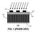
- FIG. 1presents a diagram illustrating an exemplary homojunction solar cell based on a crystalline-Si (c-Si) substrate (prior art).
- Solar cell 100includes a front side electrode grid 102 , an anti-reflective SiN layer 104 , an n + c-Si emitter layer 106 , a p-type c-Si substrate 108 , and an aluminum (Al) backside electrode 110 .
- Arrows in FIG. 1indicate incident sunlight.
- standard operationsinclude screen-printing and firing of Al paste.
- Alforms a eutectic alloy with Si at a temperature of 577° C.
- a liquid Al—Si phaseis formed according to the Al—Si phase diagram.
- the molten Al—Si regionacts as a sink for many impurities, giving a perfect gettering effect.
- the p + region generated by the firing of Alforms a back surface field (BSF), which introduce a barrier to minority carrier flow to the back surface of the solar cell. Note that the whole backside of the solar cell needs to be covered by the Al paste to ensure sufficient passivation.
- BSFback surface field
- One embodiment of the present inventionprovides a solar cell.
- the solar cellincludes a substrate, a first heavily doped crystalline-Si (c-Si) layer situated above the substrate, a lightly doped c-Si layer situated above the first heavily doped crystalline-Si layer, a second heavily doped c-Si layer situated above the lightly doped c-Si layer, a front side electrode grid situated above the second heavily doped c-Si layer, and a backside electrode grid situated on the backside of the substrate.
- c-Sicrystalline-Si
- the substrateis an MG-Si substrate.
- the backside electrode gridcomprises Al paste.
- the Al pasteincludes Al and one or more of the following materials: frit, Ag, Pd, Cr, Zn, and Sn.
- the backside electrode gridis formed using screen-printing or aerosol-jet printing.
- the backside electrode gridis solderable, and the backside electrode grid is formed using a single printing step.
- the backside electrode grid patternincludes one or more of: straight lines, crossed lines, zigzagged lines, and circles.
- the first heavily doped c-Si layer and the lightly doped c-Si layerare p-type doped, and the second heavily doped c-Si layer is n-type doped.
- the first heavily doped c-Si layer and the lightly doped c-Si layerare deposited using a chemical-vapor-deposition (CVD) technique.
- CVDchemical-vapor-deposition
- the solar cellfurther includes a dielectric layer stack situated above the second heavily doped c-Si layer.
- the dielectric layer stackincludes at least one of: SiO2, SiNx:H, and SiOxNy.
- FIG. 1presents a diagram illustrating an exemplary homojunction solar cell based on a crystalline-Si substrate (prior art).
- FIG. 2presents a diagram illustrating the process of fabricating a solar cell in accordance with an embodiment of the present invention.
- Embodiments of the present inventionprovide a solar cell that uses an Al grid as a backside electrode.
- a thin layer of heavily p-type doped c-Siis deposited on a metallurgical-grade Si (MG-Si) substrate forming a back-surface-field (BSF) layer, and a thin layer of lightly p-type doped c-Si is deposited on the BSF layer to form a base layer.
- the emitter layercan be formed by depositing a heavily n-type doped c-Si layer or by diffusing n-type dopants, such as phosphorous, at a high temperature.
- a dielectric layer stackthat includes one or more of silicon oxy-nitride (SiO x N y ), silicon-dioxide (SiO 2 ), and hydrogen-rich silicon-nitride (SiN x :H) is used for passivation and anti-reflection.
- SiO x N ysilicon oxy-nitride
- SiO 2silicon-dioxide
- SiN x :Hhydrogen-rich silicon-nitride
- FIG. 2presents a diagram illustrating the process of fabricating a solar cell in accordance with an embodiment of the present invention.
- an MG-Si substrate 200is prepared. Because MG-Si is much cheaper than c-Si, solar cells based on MG-Si substrates have a significantly lower manufacture cost. The purity of MG-Si is usually between 98% and 99.99%. To ensure a high efficiency of the subsequently fabricated solar cell, the starting MG-Si substrate ideally has a purity of 99.9% or better. In addition, the surface of the MG-Si substrate needs to be further purified. In one embodiment, MG-Si substrate 200 is baked at a temperature between 1100° C. and 1250° C. in a chemical-vapor-deposition (CVD) chamber filled with hydrogen (H 2 ) in order to remove native silicon-oxide in the substrate.
- CVDchemical-vapor-deposition
- HClhydrogen chloride
- MG-Si substrate 200can be either p-type doped or n-type doped. In one embodiment, MG-Si substrate 200 is p-type doped.
- a thin layer of heavily doped (with a doping concentration of greater than 1 ⁇ 10 17 /cm 3 ) c-Si film 202is epitaxially grown on the surface of MG-Si substrate 200 .
- Various methodscan be used to epitaxially grow c-Si thin film 202 on MG-Si substrate 200 .
- c-Si thin film 202is grown using a CVD process, such as plasma-enhanced CVD (PECVD).
- PECVDplasma-enhanced CVD
- Si compoundssuch as SiH 4 , SiH 2 Cl 2 , and SiHCl 3 , can be used in the CVD process to form c-Si thin film 202 .
- C-Si thin film 202can be either p-type doped or n-type doped.
- boronis added to make thin film 202 p-type doped.
- the doping concentration of thin film 202can be between 1 ⁇ 10 17 /cm 3 and 1 ⁇ 10 20 /cm 3 , and the thickness of thin film 202 can be between 1 ⁇ m and 8 ⁇ m.
- BSFback-surface field
- a layer of lightly doped (with a doping concentration of less than 5 ⁇ 10 17 /cm 3 ) c-Si base film 204is epitaxially grown on top of thin film 202 .
- the growing process of base film 204can be similar to that used for thin film 202 .
- base film 204can be either p-type doped or n-type doped.
- base film 204is lightly doped with a p-type dopant, such as boron.
- the doping concentration of base film 204can be between 5 ⁇ 10 15 /cm 3 and 5 ⁇ 10 17 /cm 3 , and the thickness of base film 204 can be between 5 ⁇ m and 100 ⁇ m.
- embodiments of the present inventionuse an epitaxially grown crystalline-Si film as a base layer, which can be much thinner than a c-Si wafer. As a result, the manufacture cost of solar cells can be significantly reduced.
- the surface of base film 204can be textured to maximize light absorption inside the solar cell, thus further enhancing efficiency.
- the surface texturingcan be performed using various etching techniques including dry plasma etching and wet chemical etching.
- the etchants used in the dry plasma etchinginclude, but are not limited to: SF 6 , F 2 , and NF 3 .
- the wet chemical etchantcan be an alkaline solution.
- the shapes of the surface texturecan be pyramids or inverted pyramids, which are randomly or regularly distributed on the surface of base film 204 .
- emitter layer 206can be either n-type doped or p-type doped. In one embodiment, emitter layer 206 is heavily doped with an n-type dopant, such as phosphorus. The doping concentration of emitter layer 206 can be between 5 ⁇ 10 17 /cm 3 and 5 ⁇ 10 20 /cm 3 . In one embodiment, emitter layer 206 can be formed by diffusing ions in a diffusion chamber or by in-situ doping in the CVD chamber where base film 204 is formed. In a further embodiment, emitter layer 206 can be formed using a CVD process, such as PECVD.
- SiO 2 layer 208can be formed using different oxidation techniques including dry oxidation, rapid thermal oxidation (RTO), and wet oxidation.
- SiO 2 layer 208can be formed by flowing oxygen (O 2 ) over the surface of emitter layer 206 at a high temperature between 700° C. and 1050° C.
- the thickness of SiO 2 layer 208can be between 10 ⁇ and 300 ⁇ , preferably between 100 ⁇ and 200 ⁇ .
- SiO 2 layer 208can further reduce minority-carrier surface recombination, because the oxide growth can effectively remove Si surface interstitial defects, thus passivating the dangling bonds.
- SiN x :H layer 210a relatively thick layer of SiN x :H (layer 210 ) is deposited on top of SiO 2 layer 208 .
- Techniques used for depositing SiN x :H layer 210include, but are not limited to: PECVD, sputtering, and electron beam (e-beam) evaporation.
- SiN x :H layer 210also acts as an anti-reflective layer.
- SiN x :H layer 210has a thickness between 500 ⁇ and 1000 ⁇ .
- other materials, such as ZnS and TiO 2can also be used to form an anti-reflective layer.
- a frontside metal grid 212is formed by screen printing Ag paste on top of SiN x :H layer 210 . During the screen printing process, Ag paste is forced through a patterned screen to form a metal pattern on the front surface of the solar cell.
- front side metal grid 212is formed by aerosol-jet printing Ag ink with glass frit.
- FIG. 2Iillustrates the top view of front side electrode grid 212 .
- Front side electrode grid 212includes busbars, such as busbars 216 and 218 , and fingers, such as fingers 220 and 222 . Busbars are thicker metal strips connected directly to the external leads, and fingers are finer metal strips that collect current for delivery to the busbars.
- finger strips of a backside metal grid 214are formed by screen-printing or aerosol-jet printing Al paste on the backside of MG-Si substrate 200 .
- FIG. 2Killustrates the bottom view of the solar cell. Note that the Al finger strips do not run all the way across the backside of the solar cell, leaving empty spaces for forming solderable busbars. Also note that, in addition to straight lines, Al finger strips can also take other geometric forms, including, but not limited to: crossed lines, zigzagged lines, and circles. In some embodiments, Al finger strips form irregular patterns. There is a trade-off between the sheet resistivity of the Al finger strip and the cost of Al. In one embodiment, Al finger strips covers roughly 10% of the back surface of the solar cell. Compared with a solar cell with its whole backside covered by Al, the cost to fabricate the solar cell with the patterned backside Al electrode is reduced because only 10% Al is needed.
- solderable busbarsare formed on the backside of MG-Si substrate 200 .
- Solderable busbars 224 and 226connect to external leads and collect current from the Al finger strips.
- busbars 224 and 226are formed by screen-printing or aerosol-jet printing Ag paste.
- operation 2 J and operation 2 Lcan be combined into a single operation that prints both the fingers and the busbars.
- the printing material that is used to form finger strips and busbars in a single operationincludes Al paste (a mixture of Al, glass frit, and solvent) mixed with one or more of other metals including, but not limited to: Ag, Pd, Cr, Zn, and Sn.
- front side metal grid 212 and backside metal grid 214are co-fired at a temperature above 500° C. to form front side and backside ohmic contact.
- front side metal grid 212becomes front side electrode grid 228
- backside metal grid 214becomes backside electrode grid 230 .
- photolithographyis needed to open a window in SiO 2 layer 208 and SiN x :H layer 210 .
- Such a lithographic processis expensive and is not suitable for low-cost, large-scale solar cell manufacture.
- Ag pastecan etch through SiO 2 layer 208 and SiN x :H layer 210 to make a good ohmic contact with emitter layer 206 .
- MG-Si substrate and a patterned backside electrodegreatly reduces the fabrication cost, making it possible to fabricate solar cells at a price that is below $1/Wp.
- the inclusion of a heavily doped c-Si layer acting as BSFensures the high efficiency (>17%) of the fabricated solar cell.
- using a patterned backside electrodealso solves the wafer-warping problem, which is often caused by the thick layer of Al paste on the backside of a wafer, making using a thinner ( ⁇ 50 ⁇ m) substrate possible.
Landscapes
- Life Sciences & Earth Sciences (AREA)
- Sustainable Development (AREA)
- Engineering & Computer Science (AREA)
- Sustainable Energy (AREA)
- Photovoltaic Devices (AREA)
- Chemical & Material Sciences (AREA)
- Crystallography & Structural Chemistry (AREA)
Abstract
Description
Claims (11)
Priority Applications (2)
| Application Number | Priority Date | Filing Date | Title |
|---|---|---|---|
| US12/617,382US9012766B2 (en) | 2009-11-12 | 2009-11-12 | Aluminum grid as backside conductor on epitaxial silicon thin film solar cells |
| US14/691,403US10084099B2 (en) | 2009-11-12 | 2015-04-20 | Aluminum grid as backside conductor on epitaxial silicon thin film solar cells |
Applications Claiming Priority (1)
| Application Number | Priority Date | Filing Date | Title |
|---|---|---|---|
| US12/617,382US9012766B2 (en) | 2009-11-12 | 2009-11-12 | Aluminum grid as backside conductor on epitaxial silicon thin film solar cells |
Related Child Applications (1)
| Application Number | Title | Priority Date | Filing Date |
|---|---|---|---|
| US14/691,403ContinuationUS10084099B2 (en) | 2009-11-12 | 2015-04-20 | Aluminum grid as backside conductor on epitaxial silicon thin film solar cells |
Publications (2)
| Publication Number | Publication Date |
|---|---|
| US20110108100A1 US20110108100A1 (en) | 2011-05-12 |
| US9012766B2true US9012766B2 (en) | 2015-04-21 |
Family
ID=43973233
Family Applications (2)
| Application Number | Title | Priority Date | Filing Date |
|---|---|---|---|
| US12/617,382Active2030-08-04US9012766B2 (en) | 2009-11-12 | 2009-11-12 | Aluminum grid as backside conductor on epitaxial silicon thin film solar cells |
| US14/691,403Active2030-10-15US10084099B2 (en) | 2009-11-12 | 2015-04-20 | Aluminum grid as backside conductor on epitaxial silicon thin film solar cells |
Family Applications After (1)
| Application Number | Title | Priority Date | Filing Date |
|---|---|---|---|
| US14/691,403Active2030-10-15US10084099B2 (en) | 2009-11-12 | 2015-04-20 | Aluminum grid as backside conductor on epitaxial silicon thin film solar cells |
Country Status (1)
| Country | Link |
|---|---|
| US (2) | US9012766B2 (en) |
Families Citing this family (6)
| Publication number | Priority date | Publication date | Assignee | Title |
|---|---|---|---|---|
| US8524524B2 (en) | 2010-04-22 | 2013-09-03 | General Electric Company | Methods for forming back contact electrodes for cadmium telluride photovoltaic cells |
| US20120312361A1 (en)* | 2011-06-08 | 2012-12-13 | International Business Machines Corporation | Emitter structure and fabrication method for silicon heterojunction solar cell |
| KR101428841B1 (en) | 2011-07-25 | 2014-08-14 | 한국에너지기술연구원 | Solar-cell comprising back-side electrode with grid structure |
| US10840400B2 (en)* | 2013-08-29 | 2020-11-17 | Taiwan Semiconductor Manufacturing Co., Ltd. | Photovoltaic device with back reflector |
| RU2624990C1 (en)* | 2016-09-15 | 2017-07-11 | Общество с ограниченной ответственностью "НТЦ тонкопленочных технологий в энергетике", ООО "НТЦ ТПТ" | Contact grid of heterotransitional photoelectric converter based on silicon and method of its manufacture |
| CN114050190B (en) | 2021-11-19 | 2024-02-13 | 常州时创能源股份有限公司 | Double-sided passivation contact battery and preparation method thereof |
Citations (13)
| Publication number | Priority date | Publication date | Assignee | Title |
|---|---|---|---|---|
| US3961997A (en)* | 1975-05-12 | 1976-06-08 | The United States Of America As Represented By The Administrator Of The National Aeronautics And Space Administration | Fabrication of polycrystalline solar cells on low-cost substrates |
| US4015280A (en)* | 1974-10-19 | 1977-03-29 | Sony Corporation | Multi-layer semiconductor photovoltaic device |
| US5726065A (en)* | 1995-02-21 | 1998-03-10 | Imec Vzw | Method of preparing solar cell front contacts |
| US6333457B1 (en)* | 2000-08-29 | 2001-12-25 | Sunpower Corporation | Edge passivated silicon solar/photo cell and method of manufacture |
| US6552414B1 (en)* | 1996-12-24 | 2003-04-22 | Imec Vzw | Semiconductor device with selectively diffused regions |
| US20050109388A1 (en)* | 2003-11-05 | 2005-05-26 | Canon Kabushiki Kaisha | Photovoltaic device and manufacturing method thereof |
| US20050133084A1 (en)* | 2003-10-10 | 2005-06-23 | Toshio Joge | Silicon solar cell and production method thereof |
| US20060060238A1 (en)* | 2004-02-05 | 2006-03-23 | Advent Solar, Inc. | Process and fabrication methods for emitter wrap through back contact solar cells |
| US20060231803A1 (en)* | 2005-04-14 | 2006-10-19 | Yueli Wang | Electroconductive thick film composition(s), electrode(s), and semiconductor device(s) formed therefrom |
| US20070202029A1 (en)* | 2003-12-04 | 2007-08-30 | Gary Burns | Method Of Removing Impurities From Metallurgical Grade Silicon To Produce Solar Grade Silicon |
| US20080196757A1 (en)* | 2007-02-19 | 2008-08-21 | Sanyo Electric Co., Ltd. | Solar cell and solar cell module |
| US20090101872A1 (en)* | 2007-10-18 | 2009-04-23 | E.I. Du Pont De Nemours And Company | LEAD-FREE CONDUCTIVE COMPOSITIONS AND PROCESSES FOR USE IN THE MANUFACTURE OF SEMICONDUCTOR DEVICES: Mg-CONTAINING ADDITIVE |
| US20100065111A1 (en)* | 2008-09-16 | 2010-03-18 | Sierra Solar Power, Inc. | Solar cells fabricated by using cvd epitaxial si films on metallurgical-grade si wafers |
Family Cites Families (452)
| Publication number | Priority date | Publication date | Assignee | Title |
|---|---|---|---|---|
| US819360A (en) | 1905-03-22 | 1906-05-01 | Edward Newton A | Electrical switch. |
| US2626907A (en) | 1951-05-14 | 1953-01-27 | Petrolite Corp | Process for breaking petroleum emulsions |
| US2938938A (en) | 1956-07-03 | 1960-05-31 | Hoffman Electronics Corp | Photo-voltaic semiconductor apparatus or the like |
| US3116171A (en) | 1961-03-14 | 1963-12-31 | Bell Telephone Labor Inc | Satellite solar cell assembly |
| US3094439A (en) | 1961-07-24 | 1963-06-18 | Spectrolab | Solar cell system |
| US3459597A (en) | 1966-02-04 | 1969-08-05 | Trw Inc | Solar cells with flexible overlapping bifurcated connector |
| US3676179A (en) | 1968-10-03 | 1972-07-11 | Gulf Oil Corp | Coated article and method for making same |
| US3969163A (en) | 1974-09-19 | 1976-07-13 | Texas Instruments Incorporated | Vapor deposition method of forming low cost semiconductor solar cells including reconstitution of the reacted gases |
| US4082568A (en) | 1977-05-10 | 1978-04-04 | Joseph Lindmayer | Solar cell with multiple-metal contacts |
| US4193975A (en) | 1977-11-21 | 1980-03-18 | Union Carbide Corporation | Process for the production of improved refined metallurgical silicon |
| US4124410A (en) | 1977-11-21 | 1978-11-07 | Union Carbide Corporation | Silicon solar cells with low-cost substrates |
| US4342044A (en) | 1978-03-08 | 1982-07-27 | Energy Conversion Devices, Inc. | Method for optimizing photoresponsive amorphous alloys and devices |
| US4200621A (en) | 1978-07-18 | 1980-04-29 | Motorola, Inc. | Sequential purification and crystal growth |
| US4284490A (en) | 1978-09-28 | 1981-08-18 | Coulter Systems Corporation | R.F. Sputtering apparatus including multi-network power supply |
| US4213798A (en) | 1979-04-27 | 1980-07-22 | Rca Corporation | Tellurium schottky barrier contact for amorphous silicon solar cells |
| US4251285A (en) | 1979-08-14 | 1981-02-17 | Westinghouse Electric Corp. | Diffusion of dopant from optical coating and single step formation of PN junction in silicon solar cell and coating thereon |
| DE2944185A1 (en) | 1979-11-02 | 1981-05-07 | Licentia Patent-Verwaltungs-Gmbh, 6000 Frankfurt | SOLAR CELL |
| US4315096A (en) | 1980-07-25 | 1982-02-09 | Eastman Kodak Company | Integrated array of photovoltaic cells having minimized shorting losses |
| JPS5789269A (en) | 1980-09-26 | 1982-06-03 | Licentia Gmbh | Solar battery unit |
| EP0078541B1 (en) | 1981-11-04 | 1991-01-16 | Kanegafuchi Kagaku Kogyo Kabushiki Kaisha | Flexible photovoltaic device |
| US4571448A (en) | 1981-11-16 | 1986-02-18 | University Of Delaware | Thin film photovoltaic solar cell and method of making the same |
| US4657060A (en) | 1982-03-01 | 1987-04-14 | Graber Industries, Inc. | Vertical venetian blind with inline drive |
| US4431858A (en) | 1982-05-12 | 1984-02-14 | University Of Florida | Method of making quasi-grain boundary-free polycrystalline solar cell structure and solar cell structure obtained thereby |
| DE3308269A1 (en) | 1983-03-09 | 1984-09-13 | Licentia Patent-Verwaltungs-Gmbh | SOLAR CELL |
| US4586988A (en) | 1983-08-19 | 1986-05-06 | Energy Conversion Devices, Inc. | Method of forming an electrically conductive member |
| US4589191A (en) | 1983-10-20 | 1986-05-20 | Unisearch Limited | Manufacture of high efficiency solar cells |
| US4514579A (en) | 1984-01-30 | 1985-04-30 | Energy Conversion Devices, Inc. | Large area photovoltaic cell and method for producing same |
| DE3419137A1 (en) | 1984-05-23 | 1985-11-28 | Bayer Ag, 5090 Leverkusen | METHOD AND DEVICE FOR PRODUCING SEMICONDUCTOR FILMS |
| US4577051A (en) | 1984-09-28 | 1986-03-18 | The Standard Oil Company | Bypass diode assembly for photovoltaic modules |
| US4567642A (en) | 1984-09-28 | 1986-02-04 | The Standard Oil Company | Method of making photovoltaic modules |
| US4633033A (en) | 1985-02-08 | 1986-12-30 | Energy Conversion Devices, Inc. | Photovoltaic device and method |
| US4617421A (en) | 1985-04-01 | 1986-10-14 | Sovonics Solar Systems | Photovoltaic cell having increased active area and method for producing same |
| US4667060A (en) | 1985-05-28 | 1987-05-19 | Spire Corporation | Back junction photovoltaic solar cell |
| US4652693A (en) | 1985-08-30 | 1987-03-24 | The Standard Oil Company | Reformed front contact current collector grid and cell interconnect for a photovoltaic cell module |
| US4753683A (en) | 1985-09-09 | 1988-06-28 | Hughes Aircraft Company | Gallium arsenide solar cell system |
| FR2597662B1 (en) | 1986-04-22 | 1988-06-17 | Thomson Csf | PIN PHOTODIODE MADE FROM AMORPHOUS SEMICONDUCTOR |
| US4729970A (en) | 1986-09-15 | 1988-03-08 | Energy Conversion Devices, Inc. | Conversion process for passivating short circuit current paths in semiconductor devices |
| US4694115A (en) | 1986-11-04 | 1987-09-15 | Spectrolab, Inc. | Solar cell having improved front surface metallization |
| DE3708548A1 (en) | 1987-03-17 | 1988-09-29 | Telefunken Electronic Gmbh | SOLAR CELL MODULE WITH PARALLEL AND SERIAL ARRANGED SOLAR CELLS |
| US4771017A (en) | 1987-06-23 | 1988-09-13 | Spire Corporation | Patterning process |
| US5057163A (en)* | 1988-05-04 | 1991-10-15 | Astropower, Inc. | Deposited-silicon film solar cell |
| US5698451A (en) | 1988-06-10 | 1997-12-16 | Mobil Solar Energy Corporation | Method of fabricating contacts for solar cells |
| US5075763A (en) | 1988-09-28 | 1991-12-24 | Kopin Corporation | High temperature metallization system for contacting semiconductor materials |
| JPH06105691B2 (en) | 1988-09-29 | 1994-12-21 | 株式会社富士電機総合研究所 | Method for producing carbon-doped amorphous silicon thin film |
| US4933061A (en) | 1988-12-29 | 1990-06-12 | Trifari, Krussman & Fishel, Inc. | Electroplating tank |
| DE3901042A1 (en) | 1989-01-14 | 1990-07-26 | Nukem Gmbh | METHOD AND DEVICE FOR PRODUCING A SEMICONDUCTOR LAYER SYSTEM |
| US5091018A (en) | 1989-04-17 | 1992-02-25 | The Boeing Company | Tandem photovoltaic solar cell with III-V diffused junction booster cell |
| US5118361A (en) | 1990-05-21 | 1992-06-02 | The Boeing Company | Terrestrial concentrator solar cell module |
| US5217539A (en) | 1991-09-05 | 1993-06-08 | The Boeing Company | III-V solar cells and doping processes |
| JPH036867A (en) | 1989-06-05 | 1991-01-14 | Mitsubishi Electric Corp | Electrode structure of photovoltaic device, forming method, and apparatus for manufacture thereof |
| DE4009336A1 (en) | 1990-03-23 | 1991-09-26 | Telefunken Systemtechnik | SOLAR CELL |
| CA2082819C (en) | 1990-05-18 | 2001-10-02 | Bp Chemicals (Hitco) Inc. | Materials for chemical vapor deposition processes |
| DK170189B1 (en) | 1990-05-30 | 1995-06-06 | Yakov Safir | Process for the manufacture of semiconductor components, as well as solar cells made therefrom |
| US5155051A (en) | 1990-06-22 | 1992-10-13 | Sanyo Electric Co., Ltd. | Method of manufacturing photovoltaic device |
| US5213628A (en) | 1990-09-20 | 1993-05-25 | Sanyo Electric Co., Ltd. | Photovoltaic device |
| DE4030713A1 (en) | 1990-09-28 | 1992-04-02 | Telefunken Systemtechnik | Photoelectric solar generator - has flexible intermediate connecting plate designed to prevent solar cell fracture due to temp. change stresses |
| JPH04245683A (en) | 1991-01-31 | 1992-09-02 | Tonen Corp | Manufacture of solar cell |
| US5364518A (en) | 1991-05-28 | 1994-11-15 | Leybold Aktiengesellschaft | Magnetron cathode for a rotating target |
| US5178685A (en) | 1991-06-11 | 1993-01-12 | Mobil Solar Energy Corporation | Method for forming solar cell contacts and interconnecting solar cells |
| ES2115671T3 (en) | 1991-06-11 | 1998-07-01 | Ase Americas Inc | IMPROVED SOLAR CELL AND METHOD FOR THE MANUFACTURE OF THE SAME. |
| US5181968A (en) | 1991-06-24 | 1993-01-26 | United Solar Systems Corporation | Photovoltaic device having an improved collector grid |
| US5455430A (en) | 1991-08-01 | 1995-10-03 | Sanyo Electric Co., Ltd. | Photovoltaic device having a semiconductor grade silicon layer formed on a metallurgical grade substrate |
| US5705828A (en) | 1991-08-10 | 1998-01-06 | Sanyo Electric Co., Ltd. | Photovoltaic device |
| US5286306A (en) | 1992-02-07 | 1994-02-15 | Shalini Menezes | Thin film photovoltaic cells from I-III-VI-VII compounds |
| US5808315A (en) | 1992-07-21 | 1998-09-15 | Semiconductor Energy Laboratory Co., Ltd. | Thin film transistor having transparent conductive film |
| JPH06196766A (en) | 1992-12-24 | 1994-07-15 | Fujitsu Ltd | Superconducting transistor |
| JPH0794431A (en) | 1993-04-23 | 1995-04-07 | Canon Inc | Substrate for amorphous semiconductor, amorphous semiconductor substrate having the substrate, and method for manufacturing the amorphous semiconductor substrate |
| US5401331A (en) | 1993-09-07 | 1995-03-28 | Midwest Research Institute | Substrate for thin silicon solar cells |
| JP3265077B2 (en) | 1993-09-22 | 2002-03-11 | 株式会社東芝 | ID card making machine and ID card making method |
| DE4333407C1 (en) | 1993-09-30 | 1994-11-17 | Siemens Ag | Solar cell comprising a chalcopyrite absorber layer |
| JPH07249788A (en) | 1994-03-11 | 1995-09-26 | Tonen Corp | Solar cell |
| JPH07326664A (en) | 1994-05-31 | 1995-12-12 | Fuji Electric Co Ltd | Wafer dielectric isolation trench filling method |
| FR2722612B1 (en) | 1994-07-13 | 1997-01-03 | Centre Nat Rech Scient | METHOD FOR MANUFACTURING A PHOTOVOLTAIC MATERIAL OR DEVICE, MATERIAL OR DEVICE THUS OBTAINED AND PHOTOPILE COMPRISING SUCH A MATERIAL OR DEVICE |
| JP2992464B2 (en) | 1994-11-04 | 1999-12-20 | キヤノン株式会社 | Covering wire for current collecting electrode, photovoltaic element using the covering wire for current collecting electrode, and method of manufacturing the same |
| US5627081A (en) | 1994-11-29 | 1997-05-06 | Midwest Research Institute | Method for processing silicon solar cells |
| EP0822996B1 (en) | 1995-04-25 | 2003-07-02 | VON ARDENNE ANLAGENTECHNIK GmbH | Sputtering system using cylindrical rotating magnetron electrically powered using alternating current |
| JP3459947B2 (en) | 1996-06-18 | 2003-10-27 | シャープ株式会社 | Solar cell manufacturing method |
| US6017581A (en) | 1997-04-18 | 2000-01-25 | Semi-Alloys Company | Method for coating lenticular articles |
| JPH1131834A (en) | 1997-07-10 | 1999-02-02 | Showa Shell Sekiyu Kk | Glass sandwich solar panel |
| US6091019A (en) | 1997-09-26 | 2000-07-18 | Sanyo Electric Co., Ltd. | Photovoltaic element and manufacturing method thereof |
| US6140570A (en) | 1997-10-29 | 2000-10-31 | Canon Kabushiki Kaisha | Photovoltaic element having a back side transparent and electrically conductive layer with a light incident side surface region having a specific cross section and a module comprising said photovolatic element |
| US5903382A (en) | 1997-12-19 | 1999-05-11 | Rockwell International Corporation | Electrodeposition cell with high light transmission |
| DE59915079D1 (en) | 1998-03-13 | 2009-10-22 | Willeke Gerhard | SOLAR CELL ARRANGEMENT AND METHOD FOR PRODUCING A SOLAR CELL ARRANGEMENT |
| DE69943141D1 (en) | 1998-05-20 | 2011-03-03 | Canon Kk | Photovoltaic power generation device |
| US20070108437A1 (en) | 1998-06-08 | 2007-05-17 | Avto Tavkhelidze | Method of fabrication of high temperature superconductors based on new mechanism of electron-electron interaction |
| US6468828B1 (en) | 1998-07-14 | 2002-10-22 | Sky Solar L.L.C. | Method of manufacturing lightweight, high efficiency photovoltaic module |
| US6303853B1 (en) | 1998-08-06 | 2001-10-16 | Jx Crystals Inc. | Shingle circuits for thermophotovoltaic systems |
| US6232545B1 (en) | 1998-08-06 | 2001-05-15 | Jx Crystals Inc. | Linear circuit designs for solar photovoltaic concentrator and thermophotovoltaic applications using cell and substrate materials with matched coefficients of thermal expansion |
| CN1134071C (en) | 1998-11-04 | 2004-01-07 | 北京市太阳能研究所 | Efficient solar battery and its making method |
| US6488824B1 (en) | 1998-11-06 | 2002-12-03 | Raycom Technologies, Inc. | Sputtering apparatus and process for high rate coatings |
| JP2000164902A (en) | 1998-11-27 | 2000-06-16 | Kyocera Corp | Solar cell |
| US8222513B2 (en) | 2006-04-13 | 2012-07-17 | Daniel Luch | Collector grid, electrode structures and interconnect structures for photovoltaic arrays and methods of manufacture |
| US20080011350A1 (en) | 1999-03-30 | 2008-01-17 | Daniel Luch | Collector grid, electrode structures and interconnect structures for photovoltaic arrays and other optoelectric devices |
| US8076568B2 (en) | 2006-04-13 | 2011-12-13 | Daniel Luch | Collector grid and interconnect structures for photovoltaic arrays and modules |
| US7635810B2 (en) | 1999-03-30 | 2009-12-22 | Daniel Luch | Substrate and collector grid structures for integrated photovoltaic arrays and process of manufacture of such arrays |
| US6034322A (en) | 1999-07-01 | 2000-03-07 | Space Systems/Loral, Inc. | Solar cell assembly |
| JP2001148500A (en) | 1999-11-22 | 2001-05-29 | Sanyo Electric Co Ltd | Solar cell module |
| KR100768414B1 (en) | 2000-03-13 | 2007-10-18 | 소니 가부시끼 가이샤 | Optical energy converter |
| US6538193B1 (en) | 2000-04-21 | 2003-03-25 | Jx Crystals Inc. | Thermophotovoltaic generator in high temperature industrial process |
| US6586270B2 (en) | 2000-06-01 | 2003-07-01 | Canon Kabushiki Kaisha | Process for producing a photovoltaic element |
| JP5081345B2 (en) | 2000-06-13 | 2012-11-28 | 富士フイルム株式会社 | Method for manufacturing photoelectric conversion element |
| DE10042733A1 (en) | 2000-08-31 | 2002-03-28 | Inst Physikalische Hochtech Ev | Multicrystalline laser-crystallized silicon thin-film solar cell on a transparent substrate |
| JP3490964B2 (en) | 2000-09-05 | 2004-01-26 | 三洋電機株式会社 | Photovoltaic device |
| JP2002134484A (en) | 2000-10-19 | 2002-05-10 | Asm Japan Kk | Semiconductor substrate holding device |
| US20020189939A1 (en) | 2001-06-14 | 2002-12-19 | German John R. | Alternating current rotatable sputter cathode |
| US6620645B2 (en) | 2000-11-16 | 2003-09-16 | G.T. Equipment Technologies, Inc | Making and connecting bus bars on solar cells |
| JP4055358B2 (en) | 2000-12-12 | 2008-03-05 | サンケン電気株式会社 | Semiconductor device and manufacturing method thereof |
| US20030021004A1 (en) | 2000-12-19 | 2003-01-30 | Cunningham Shawn Jay | Method for fabricating a through-wafer optical MEMS device having an anti-reflective coating |
| CN1291502C (en) | 2001-03-19 | 2006-12-20 | 信越半导体株式会社 | Solar cell and manufacturing method thereof |
| FR2822436B1 (en) | 2001-03-21 | 2003-08-15 | Cit Alcatel | SOLAR PANEL HAVING ELECTRICAL TERMINALS DISTRIBUTED ON ITS SURFACE |
| WO2002091692A1 (en) | 2001-04-13 | 2002-11-14 | Girard Gregory D | Ditributed edge switching system for voice-over-packet multiservice network |
| US7173275B2 (en) | 2001-05-21 | 2007-02-06 | Regents Of The University Of Colorado | Thin-film transistors based on tunneling structures and applications |
| JP2003069055A (en) | 2001-06-13 | 2003-03-07 | Sharp Corp | Solar cell and method of manufacturing the same |
| US7399385B2 (en) | 2001-06-14 | 2008-07-15 | Tru Vue, Inc. | Alternating current rotatable sputter cathode |
| US20030000568A1 (en) | 2001-06-15 | 2003-01-02 | Ase Americas, Inc. | Encapsulated photovoltaic modules and method of manufacturing same |
| US6713670B2 (en) | 2001-08-17 | 2004-03-30 | Composite Optics, Incorporated | Electrostatically clean solar array |
| WO2003019598A1 (en) | 2001-08-27 | 2003-03-06 | Northwestern University | High work function transparent conducting oxides as anodes for organic light-emitting diodes |
| US6664589B2 (en) | 2001-08-30 | 2003-12-16 | Micron Technology, Inc. | Technique to control tunneling currents in DRAM capacitors, cells, and devices |
| US6563040B2 (en) | 2001-10-11 | 2003-05-13 | Pinnacle West Capital Corporation | Structure for supporting a photovoltaic module in a solar energy collection system |
| US6672018B2 (en) | 2001-10-12 | 2004-01-06 | Jefferson Shingleton | Solar module mounting method and clip |
| US7469299B2 (en) | 2001-10-25 | 2008-12-23 | Verizon Business Global Llc | Bridging user agent and a proxy server for supporting network services |
| CN1180486C (en) | 2001-10-31 | 2004-12-15 | 四川大学 | Transparent Conductive Film Front Electrode Crystalline Silicon Solar Cell |
| US20030116185A1 (en) | 2001-11-05 | 2003-06-26 | Oswald Robert S. | Sealed thin film photovoltaic modules |
| JP3902534B2 (en) | 2001-11-29 | 2007-04-11 | 三洋電機株式会社 | Photovoltaic device and manufacturing method thereof |
| US20030121228A1 (en) | 2001-12-31 | 2003-07-03 | Stoehr Robert P. | System and method for dendritic web solar cell shingling |
| US6736948B2 (en) | 2002-01-18 | 2004-05-18 | Von Ardenne Anlagentechnik Gmbh | Cylindrical AC/DC magnetron with compliant drive system and improved electrical and thermal isolation |
| US6683360B1 (en) | 2002-01-24 | 2004-01-27 | Fillfactory | Multiple or graded epitaxial wafers for particle or radiation detection |
| US20030154667A1 (en) | 2002-02-20 | 2003-08-21 | Dinwoodie Thomas L. | Shingle system |
| JP4070483B2 (en) | 2002-03-05 | 2008-04-02 | 三洋電機株式会社 | Photovoltaic device and manufacturing method thereof |
| US20030173217A1 (en) | 2002-03-14 | 2003-09-18 | Sputtering Components, Inc. | High-power ion sputtering magnetron |
| DE10213049A1 (en) | 2002-03-22 | 2003-10-02 | Dieter Wurczinger | Rotatable tubular cathode |
| US7388146B2 (en) | 2002-04-24 | 2008-06-17 | Jx Crystals Inc. | Planar solar concentrator power module |
| KR20030083953A (en) | 2002-04-24 | 2003-11-01 | 김홍근 | Methods for Immediately Making up account Using Gift Certificate on Credit Card Terminal and Apparatus therefor |
| US6803513B2 (en) | 2002-08-20 | 2004-10-12 | United Solar Systems Corporation | Series connected photovoltaic module and method for its manufacture |
| EP1398837A1 (en) | 2002-09-09 | 2004-03-17 | Interuniversitair Microelektronica Centrum ( Imec) | Photovoltaic device |
| US7126052B2 (en) | 2002-10-02 | 2006-10-24 | The Boeing Company | Isoelectronic surfactant induced sublattice disordering in optoelectronic devices |
| JP2004134672A (en) | 2002-10-11 | 2004-04-30 | Sony Corp | Method and apparatus for manufacturing ultra-thin semiconductor device, and method and apparatus for manufacturing ultra-thin back-illuminated solid-state imaging device |
| JP2004193350A (en) | 2002-12-11 | 2004-07-08 | Sharp Corp | Solar cell and method of manufacturing the same |
| US6870600B2 (en) | 2003-01-13 | 2005-03-22 | Nikon Corporation | Vibration-attenuation devices and methods using pressurized bellows exhibiting substantially zero lateral stiffness |
| JP2004235274A (en)* | 2003-01-28 | 2004-08-19 | Kyocera Corp | Polycrystalline silicon substrate and roughening method thereof |
| JP2004304167A (en) | 2003-03-20 | 2004-10-28 | Advanced Lcd Technologies Development Center Co Ltd | Wiring, display device, and method for forming them |
| US7388147B2 (en) | 2003-04-10 | 2008-06-17 | Sunpower Corporation | Metal contact structure for solar cell and method of manufacture |
| JP4118187B2 (en) | 2003-05-09 | 2008-07-16 | 信越半導体株式会社 | Manufacturing method of solar cell |
| US20050064247A1 (en) | 2003-06-25 | 2005-03-24 | Ajit Sane | Composite refractory metal carbide coating on a substrate and method for making thereof |
| US7560750B2 (en) | 2003-06-26 | 2009-07-14 | Kyocera Corporation | Solar cell device |
| JP3722813B2 (en) | 2003-07-08 | 2005-11-30 | 沖電気工業株式会社 | Method for forming buried wiring structure |
| WO2005013334A2 (en) | 2003-08-01 | 2005-02-10 | Sgl Carbon Ag | Holder for supporting wafers during semiconductor manufacture |
| US7455787B2 (en) | 2003-08-01 | 2008-11-25 | Sunpower Corporation | Etching of solar cell materials |
| KR101022662B1 (en) | 2003-08-05 | 2011-03-22 | 주성엔지니어링(주) | Chamber and shower head for uniform film deposition |
| US7172184B2 (en) | 2003-08-06 | 2007-02-06 | Sunpower Corporation | Substrate carrier for electroplating solar cells |
| CN100431177C (en) | 2003-09-24 | 2008-11-05 | 三洋电机株式会社 | Photovoltaic element and manufacturing method thereof |
| JP4515208B2 (en) | 2003-09-25 | 2010-07-28 | 富士フイルム株式会社 | Image processing method, apparatus, and program |
| JP2005123445A (en) | 2003-10-17 | 2005-05-12 | Canon Inc | Photovoltaic element and method for producing photovoltaic element |
| US20050189015A1 (en) | 2003-10-30 | 2005-09-01 | Ajeet Rohatgi | Silicon solar cells and methods of fabrication |
| DE10357698A1 (en) | 2003-12-09 | 2005-07-14 | Schunk Kohlenstofftechnik Gmbh | Carrier for objects to be treated and method for producing such |
| JP2005175197A (en) | 2003-12-11 | 2005-06-30 | Canon Inc | Solar cell module and manufacturing method thereof |
| US7887632B2 (en) | 2004-01-15 | 2011-02-15 | Japan Science And Technology Agency | Process for producing monocrystal thin film and monocrystal thin film device |
| WO2005074039A1 (en) | 2004-01-28 | 2005-08-11 | Kyocera Corporation | Solar battery module and photovoltaic generation device |
| EP1560272B1 (en) | 2004-01-29 | 2016-04-27 | Panasonic Intellectual Property Management Co., Ltd. | Solar cell module |
| US20080223439A1 (en) | 2004-02-19 | 2008-09-18 | Xunming Deng | Interconnected Photoelectrochemical Cell |
| EP1730788A1 (en) | 2004-02-24 | 2006-12-13 | BP Corporation North America Inc. | Process for manufacturing photovoltaic cells |
| US20050252544A1 (en) | 2004-05-11 | 2005-11-17 | Ajeet Rohatgi | Silicon solar cells and methods of fabrication |
| EP1598874A1 (en) | 2004-05-19 | 2005-11-23 | Dutch Space B.V. | Solar cell assembly |
| US7772484B2 (en) | 2004-06-01 | 2010-08-10 | Konarka Technologies, Inc. | Photovoltaic module architecture |
| FR2871157A1 (en) | 2004-06-04 | 2005-12-09 | Aventis Pharma Sa | BIARYL AROMATIC PRODUCTS, COMPOSITIONS CONTAINING SAME AND USE THEREOF |
| DE05752475T1 (en) | 2004-06-24 | 2009-09-17 | Heliodynamics Ltd., Caxton | SOLAR ENERGY COLLECTOR SYSTEMS |
| US7839022B2 (en) | 2004-07-13 | 2010-11-23 | Tigo Energy, Inc. | Device for distributed maximum power tracking for solar arrays |
| US20080149163A1 (en) | 2004-08-31 | 2008-06-26 | Ron Gangemi | System and method for mounting photovoltaic cells |
| US7087906B2 (en) | 2004-09-08 | 2006-08-08 | Nikon Corporation | Bellows with spring anti-gravity device |
| US20060130891A1 (en) | 2004-10-29 | 2006-06-22 | Carlson David E | Back-contact photovoltaic cells |
| US7432119B2 (en) | 2005-01-11 | 2008-10-07 | Semileds Corporation | Light emitting diode with conducting metal substrate |
| FR2880989B1 (en) | 2005-01-20 | 2007-03-09 | Commissariat Energie Atomique | SEMICONDUCTOR DEVICE WITH HETEROJUNCTIONS AND INTERDIGITAL STRUCTURE |
| US7723215B2 (en) | 2005-02-11 | 2010-05-25 | Sarnoff Corporation | Dark current reduction in back-illuminated imaging sensors and method of fabricating same |
| US8115093B2 (en) | 2005-02-15 | 2012-02-14 | General Electric Company | Layer-to-layer interconnects for photoelectric devices and methods of fabricating the same |
| US20080121932A1 (en) | 2006-09-18 | 2008-05-29 | Pushkar Ranade | Active regions with compatible dielectric layers |
| US7781669B2 (en) | 2005-02-25 | 2010-08-24 | Sanyo Electric Co., Ltd. | Photovoltaic cell |
| KR20060097189A (en) | 2005-03-04 | 2006-09-14 | 삼성전자주식회사 | Semiconductor device manufacturing equipment |
| DE102005013668B3 (en) | 2005-03-14 | 2006-11-16 | Universität Stuttgart | solar cell |
| US7759158B2 (en) | 2005-03-22 | 2010-07-20 | Applied Materials, Inc. | Scalable photovoltaic cell and solar panel manufacturing with improved wiring |
| JP5042819B2 (en) | 2005-03-29 | 2012-10-03 | 京セラ株式会社 | Packing method of solar cell element |
| DE102005019225B4 (en) | 2005-04-20 | 2009-12-31 | Helmholtz-Zentrum Berlin Für Materialien Und Energie Gmbh | Heterocontact solar cell with inverted layer structure geometry |
| US7375378B2 (en) | 2005-05-12 | 2008-05-20 | General Electric Company | Surface passivated photovoltaic devices |
| JP5301758B2 (en) | 2005-05-19 | 2013-09-25 | 信越半導体株式会社 | Solar cell |
| US8039731B2 (en) | 2005-06-06 | 2011-10-18 | General Electric Company | Photovoltaic concentrator for solar energy system |
| EP1734589B1 (en) | 2005-06-16 | 2019-12-18 | Panasonic Intellectual Property Management Co., Ltd. | Method for manufacturing photovoltaic module |
| CN101010448B (en) | 2005-06-23 | 2010-09-29 | 东京毅力科创株式会社 | Constitutional member for semiconductor processing apparatus and method for producing same |
| US20070023081A1 (en) | 2005-07-28 | 2007-02-01 | General Electric Company | Compositionally-graded photovoltaic device and fabrication method, and related articles |
| US7906723B2 (en) | 2008-04-30 | 2011-03-15 | General Electric Company | Compositionally-graded and structurally-graded photovoltaic devices and methods of fabricating such devices |
| US20070023082A1 (en) | 2005-07-28 | 2007-02-01 | Venkatesan Manivannan | Compositionally-graded back contact photovoltaic devices and methods of fabricating such devices |
| JP2007123792A (en) | 2005-09-28 | 2007-05-17 | Kyocera Corp | Solar cell module |
| JP5171001B2 (en) | 2005-09-30 | 2013-03-27 | 三洋電機株式会社 | Method for manufacturing solar cell module, solar cell and solar cell module |
| CN101548391B (en) | 2005-11-04 | 2012-01-25 | 陶氏康宁公司 | Encapsulation of photovoltaic cells |
| CN101305454B (en) | 2005-11-07 | 2010-05-19 | 应用材料股份有限公司 | Method for forming photovoltaic contacts and connections |
| DK1948850T3 (en) | 2005-11-18 | 2019-07-29 | Luxembourg Inst Science & Tech List | PROCEDURE FOR MAKING A MULTIPLE LAYER STRUCTURE |
| US20070132034A1 (en) | 2005-12-14 | 2007-06-14 | Giuseppe Curello | Isolation body for semiconductor devices and method to form the same |
| US20070137699A1 (en) | 2005-12-16 | 2007-06-21 | General Electric Company | Solar cell and method for fabricating solar cell |
| JP2007194580A (en) | 2005-12-21 | 2007-08-02 | E I Du Pont De Nemours & Co | Solar cell electrode paste |
| US8196360B2 (en) | 2006-01-12 | 2012-06-12 | Msr Innovations Inc. | Photovoltaic solar roof tile assembly system |
| JP5025135B2 (en) | 2006-01-24 | 2012-09-12 | 三洋電機株式会社 | Photovoltaic module |
| EP1816684A2 (en) | 2006-02-01 | 2007-08-08 | Sanyo Electric Co. Ltd. | Solar battery module |
| US7769887B1 (en) | 2006-02-03 | 2010-08-03 | Sprint Communications Company L.P. | Opportunistic data transfer over heterogeneous wireless networks |
| US8603248B2 (en) | 2006-02-10 | 2013-12-10 | Veeco Instruments Inc. | System and method for varying wafer surface temperature via wafer-carrier temperature offset |
| DE102006009194A1 (en) | 2006-02-22 | 2007-08-23 | Siegfried Gutfleisch | Arrangement of primary building structure e.g. photo-voltaic cell, consists of pre-mounted unit, with which structure of solar cell with respective segment of building structure forms assembly unit |
| CH696344A5 (en) | 2006-02-22 | 2007-04-30 | Ses Soc En Solaire Sa | Support film and method for coupling photovoltaic cells. |
| US20090014055A1 (en) | 2006-03-18 | 2009-01-15 | Solyndra, Inc. | Photovoltaic Modules Having a Filling Material |
| US20070235077A1 (en) | 2006-03-27 | 2007-10-11 | Kyocera Corporation | Solar Cell Module and Manufacturing Process Thereof |
| US8168880B2 (en) | 2006-04-26 | 2012-05-01 | Certainteed Corporation | Shingle with photovoltaic element(s) and array of same laid up on a roof |
| US7737357B2 (en) | 2006-05-04 | 2010-06-15 | Sunpower Corporation | Solar cell having doped semiconductor heterojunction contacts |
| US8571012B2 (en) | 2006-05-12 | 2013-10-29 | Oracle International Corporation | Customized sip routing to cross firewalls |
| US20080035489A1 (en) | 2006-06-05 | 2008-02-14 | Rohm And Haas Electronic Materials Llc | Plating process |
| US20070283997A1 (en) | 2006-06-13 | 2007-12-13 | Miasole | Photovoltaic module with integrated current collection and interconnection |
| US20070283996A1 (en) | 2006-06-13 | 2007-12-13 | Miasole | Photovoltaic module with insulating interconnect carrier |
| JP4290747B2 (en) | 2006-06-23 | 2009-07-08 | シャープ株式会社 | Photoelectric conversion element and photoelectric conversion element with interconnector |
| US20080000522A1 (en) | 2006-06-30 | 2008-01-03 | General Electric Company | Photovoltaic device which includes all-back-contact configuration; and related processes |
| EP2070115A2 (en) | 2006-08-04 | 2009-06-17 | SoloPower, Inc. | Thin film solar cell with finger pattern |
| US7915517B2 (en) | 2006-08-16 | 2011-03-29 | Lau Po K | Bifacial photovoltaic devices |
| US20080047602A1 (en) | 2006-08-22 | 2008-02-28 | Guardian Industries Corp. | Front contact with high-function TCO for use in photovoltaic device and method of making same |
| US7893348B2 (en) | 2006-08-25 | 2011-02-22 | General Electric Company | Nanowires in thin-film silicon solar cells |
| US20080053519A1 (en) | 2006-08-30 | 2008-03-06 | Miasole | Laminated photovoltaic cell |
| DE102006042617B4 (en) | 2006-09-05 | 2010-04-08 | Q-Cells Se | Method for generating local contacts |
| FR2906406B1 (en) | 2006-09-26 | 2008-12-19 | Commissariat Energie Atomique | PROCESS FOR PRODUCING A PHOTOVOLTAIC CELL WITH REAR-SIDE HETEROJUNCTION |
| US7999174B2 (en) | 2006-10-09 | 2011-08-16 | Solexel, Inc. | Solar module structures and assembly methods for three-dimensional thin-film solar cells |
| US20080264477A1 (en) | 2006-10-09 | 2008-10-30 | Soltaix, Inc. | Methods for manufacturing three-dimensional thin-film solar cells |
| US20080092947A1 (en) | 2006-10-24 | 2008-04-24 | Applied Materials, Inc. | Pulse plating of a low stress film on a solar cell substrate |
| DE102006051735A1 (en) | 2006-10-30 | 2008-05-08 | Merck Patent Gmbh | Printable medium for the etching of oxidic, transparent, conductive layers |
| US8013474B2 (en) | 2006-11-27 | 2011-09-06 | Xslent Energy Technologies, Llc | System and apparatuses with multiple power extractors coupled to different power sources |
| JP2008135655A (en) | 2006-11-29 | 2008-06-12 | Sanyo Electric Co Ltd | Solar battery module, manufacturing method therefor, and solar battery cell |
| US20080121276A1 (en) | 2006-11-29 | 2008-05-29 | Applied Materials, Inc. | Selective electroless deposition for solar cells |
| US7799182B2 (en) | 2006-12-01 | 2010-09-21 | Applied Materials, Inc. | Electroplating on roll-to-roll flexible solar cell substrates |
| JP4429306B2 (en) | 2006-12-25 | 2010-03-10 | 三洋電機株式会社 | Solar cell and solar cell module |
| WO2008078741A1 (en) | 2006-12-26 | 2008-07-03 | Kyocera Corporation | Solar cell module |
| US7825329B2 (en) | 2007-01-03 | 2010-11-02 | Solopower, Inc. | Thin film solar cell manufacturing and integration |
| CN101226968A (en) | 2007-01-17 | 2008-07-23 | 易斌宣 | Method for reducing series resistance of concentrating solar cell and concentrating solar cell obtained by the method |
| US20080173350A1 (en) | 2007-01-18 | 2008-07-24 | Applied Materials, Inc. | Multi-junction solar cells and methods and apparatuses for forming the same |
| US20080173347A1 (en) | 2007-01-23 | 2008-07-24 | General Electric Company | Method And Apparatus For A Semiconductor Structure |
| US8853527B2 (en) | 2007-02-16 | 2014-10-07 | Nanogram Corporation | Solar cell structures, photovoltaic panels and corresponding processes |
| US7534632B2 (en) | 2007-02-20 | 2009-05-19 | Advanced Chip Engineering Technology Inc. | Method for circuits inspection and method of the same |
| DE202007002897U1 (en) | 2007-02-28 | 2008-07-10 | SCHÜCO International KG | Photovoltaic solar module |
| US7968792B2 (en) | 2007-03-05 | 2011-06-28 | Seagate Technology Llc | Quantum dot sensitized wide bandgap semiconductor photovoltaic devices & methods of fabricating same |
| EP2135292A2 (en) | 2007-03-16 | 2009-12-23 | BP Corporation North America Inc. | Solar cells |
| EP1973167B1 (en) | 2007-03-19 | 2018-06-13 | Panasonic Intellectual Property Management Co., Ltd. | Photovoltaic device and method of manufacturing the same |
| FR2914785B1 (en) | 2007-04-06 | 2009-05-15 | Saint Gobain Ct Recherches | PHOTOVOLTAIC ROOF COATING |
| US8471141B2 (en) | 2007-05-07 | 2013-06-25 | Nanosolar, Inc | Structures for low cost, reliable solar roofing |
| US20080308145A1 (en) | 2007-06-12 | 2008-12-18 | Guardian Industries Corp | Front electrode including transparent conductive coating on etched glass substrate for use in photovoltaic device and method of making same |
| KR200438601Y1 (en) | 2007-07-13 | 2008-02-26 | 임준희 | Pencil sharpener |
| JP5288790B2 (en) | 2007-08-02 | 2013-09-11 | 三洋電機株式会社 | Solar cell module and manufacturing method thereof |
| JP5147332B2 (en) | 2007-08-27 | 2013-02-20 | 三洋電機株式会社 | SOLAR CELL MODULE, SOLAR CELL, AND MANUFACTURING METHOD THEREOF |
| US20090056797A1 (en) | 2007-08-28 | 2009-03-05 | Blue Square Energy Incorporated | Photovoltaic Thin-Film Solar Cell and Method Of Making The Same |
| US7709730B2 (en) | 2007-09-05 | 2010-05-04 | Skyline Solar, Inc. | Dual trough concentrating solar photovoltaic module |
| US7749883B2 (en) | 2007-09-20 | 2010-07-06 | Fry's Metals, Inc. | Electroformed stencils for solar cell front side metallization |
| KR101503557B1 (en) | 2007-09-25 | 2015-03-17 | 퍼스트 솔라, 인코포레이티드 | Photovoltaic devices including an interfacial layer |
| TWI371112B (en) | 2007-10-02 | 2012-08-21 | Univ Chang Gung | Solar energy photoelectric conversion apparatus |
| CN101641800A (en) | 2007-10-12 | 2010-02-03 | 系统股份公司 | Method for connecting photovoltaic cells in series, photovoltaic cells connectable in series by said method and module obtained by said method |
| GB2453746A (en) | 2007-10-16 | 2009-04-22 | Renewable Energy Corp Asa | Parallel interconnection of solar cell units |
| WO2009061963A2 (en) | 2007-11-06 | 2009-05-14 | Krause Richard H | Photovoltaic roofing systems and methods for installing them |
| KR101293162B1 (en) | 2007-11-09 | 2013-08-12 | 선프림, 리미티드 | Low-cost solar cells and methods for their production |
| US20090139512A1 (en) | 2007-11-30 | 2009-06-04 | Lima Daniel D De | Solar Line Boiler Roof |
| AT506129B1 (en) | 2007-12-11 | 2009-10-15 | Heic Hornbachner En Innovation | Curved photovoltaic modules and methods of making same |
| US8021487B2 (en) | 2007-12-12 | 2011-09-20 | Veeco Instruments Inc. | Wafer carrier with hub |
| TWI379425B (en) | 2007-12-13 | 2012-12-11 | Nexpower Technology Corp | Translucent solar cell and manufacturing method thereof |
| JP2011507306A (en) | 2007-12-17 | 2011-03-03 | クォルコム・メムズ・テクノロジーズ・インコーポレーテッド | Photovoltaic device with interference backside mask |
| US9263895B2 (en) | 2007-12-21 | 2016-02-16 | Sunpower Corporation | Distributed energy conversion systems |
| US8212139B2 (en) | 2008-01-18 | 2012-07-03 | Tenksolar, Inc. | Thin-film photovoltaic module |
| TW200947725A (en) | 2008-01-24 | 2009-11-16 | Applied Materials Inc | Improved HIT solar cell structure |
| US20090188561A1 (en) | 2008-01-25 | 2009-07-30 | Emcore Corporation | High concentration terrestrial solar array with III-V compound semiconductor cell |
| US8222516B2 (en) | 2008-02-20 | 2012-07-17 | Sunpower Corporation | Front contact solar cell with formed emitter |
| CN101978224B (en) | 2008-02-20 | 2013-10-16 | 康宁股份有限公司 | Solar heat collection element with glass-ceramic central tube |
| CN101946335B (en) | 2008-02-21 | 2012-11-21 | 夏普株式会社 | Solar cell and method for manufacturing solar cell |
| US8187906B2 (en) | 2008-02-28 | 2012-05-29 | Sunlight Photonics Inc. | Method for fabricating composite substances for thin film electro-optical devices |
| WO2009111575A2 (en) | 2008-03-05 | 2009-09-11 | Sri International | Substrates for silicon solar cells and methods of producing the same |
| US20100043863A1 (en) | 2008-03-20 | 2010-02-25 | Miasole | Interconnect assembly |
| US7833808B2 (en) | 2008-03-24 | 2010-11-16 | Palo Alto Research Center Incorporated | Methods for forming multiple-layer electrode structures for silicon photovoltaic cells |
| US20090250108A1 (en) | 2008-04-02 | 2009-10-08 | Applied Materials, Inc. | Silicon carbide for crystalline silicon solar cell surface passivation |
| US20090255574A1 (en) | 2008-04-14 | 2009-10-15 | Sierra Solar Power, Inc. | Solar cell fabricated by silicon liquid-phase deposition |
| WO2009134939A2 (en) | 2008-04-29 | 2009-11-05 | Advent Solar, Inc. | Photovoltaic modules manufactured using monolithic module assembly techniques |
| US7964499B2 (en) | 2008-05-13 | 2011-06-21 | Samsung Electronics Co., Ltd. | Methods of forming semiconductor solar cells having front surface electrodes |
| TWI513014B (en) | 2008-05-19 | 2015-12-11 | Tatung Co | High performance optoelectronic components |
| US20090293948A1 (en) | 2008-05-28 | 2009-12-03 | Stichting Energieonderzoek Centrum Nederland | Method of manufacturing an amorphous/crystalline silicon heterojunction solar cell |
| US20100229914A1 (en) | 2008-06-04 | 2010-09-16 | Solexant Corp. | Solar cells with shunt resistance |
| CN102150278A (en) | 2008-06-11 | 2011-08-10 | 因特瓦克公司 | Formation of solar cell-selective emitter using implant and anneal method |
| CN102099927A (en) | 2008-06-12 | 2011-06-15 | 耶路撒冷希伯来大学伊森姆研究发展公司 | Solar volumetric structure comprising grooves of a funnel-like shape |
| US8338218B2 (en) | 2008-06-26 | 2012-12-25 | Semiconductor Energy Laboratory Co., Ltd. | Photoelectric conversion device module and manufacturing method of the photoelectric conversion device module |
| DE102008030693A1 (en) | 2008-07-01 | 2010-01-14 | Institut Für Solarenergieforschung Gmbh | Heterojunction solar cell with absorber with integrated doping profile |
| EP2311101B1 (en) | 2008-07-03 | 2012-11-21 | Imec | Photovoltaic module and the processing thereof |
| KR101244027B1 (en) | 2008-07-08 | 2013-03-14 | 시너스 테크놀리지, 인코포레이티드 | Flexible solar cell and fabricating method for the same |
| TW201013961A (en) | 2008-07-16 | 2010-04-01 | Applied Materials Inc | Hybrid heterojunction solar cell fabrication using a metal layer mask |
| KR101065752B1 (en) | 2008-08-19 | 2011-09-19 | 주식회사 티지솔라 | Solar cell module and its manufacturing method |
| KR20100026291A (en) | 2008-08-29 | 2010-03-10 | 삼성전자주식회사 | Thin film solar cell module and method of manufacturing the same |
| DE102008045522A1 (en) | 2008-09-03 | 2010-03-04 | Fraunhofer-Gesellschaft zur Förderung der angewandten Forschung e.V. | Hetero-solar cell and process for the preparation of hetero-solar cells |
| US20150075599A1 (en) | 2013-09-19 | 2015-03-19 | Zena Technologies, Inc. | Pillar structured multijunction photovoltaic devices |
| TW201027783A (en) | 2008-09-19 | 2010-07-16 | Applied Materials Inc | Methods of making an emitter having a desired dopant profile |
| JP2010085949A (en) | 2008-10-03 | 2010-04-15 | Hitachi Displays Ltd | Liquid crystal display |
| US8070925B2 (en) | 2008-10-17 | 2011-12-06 | Applied Materials, Inc. | Physical vapor deposition reactor with circularly symmetric RF feed and DC feed to the sputter target |
| US20100108134A1 (en) | 2008-10-31 | 2010-05-06 | Crystal Solar, Inc. | Thin two sided single crystal solar cell and manufacturing process thereof |
| US8586857B2 (en) | 2008-11-04 | 2013-11-19 | Miasole | Combined diode, lead assembly incorporating an expansion joint |
| US20100116325A1 (en) | 2008-11-12 | 2010-05-13 | Mehrdad Nikoonahad | High efficiency solar panel and system |
| US9150966B2 (en) | 2008-11-14 | 2015-10-06 | Palo Alto Research Center Incorporated | Solar cell metallization using inline electroless plating |
| FR2938628B1 (en) | 2008-11-18 | 2011-01-21 | Bpb Ltd | LIGHT PLATE |
| KR100993511B1 (en) | 2008-11-19 | 2010-11-12 | 엘지전자 주식회사 | Solar cell and manufacturing method thereof |
| US20100132774A1 (en) | 2008-12-11 | 2010-06-03 | Applied Materials, Inc. | Thin Film Silicon Solar Cell Device With Amorphous Window Layer |
| EP2359407A4 (en) | 2008-12-16 | 2013-03-13 | Solopower Inc | METHODS OF MANUFACTURING AND STRUCTURES OF THIN FILM PHOTOVOLTAIC MODULE |
| DE102008055028A1 (en) | 2008-12-19 | 2010-07-01 | Q-Cells Se | solar cell |
| KR101539047B1 (en) | 2008-12-24 | 2015-07-23 | 인텔렉츄얼 키스톤 테크놀로지 엘엘씨 | Photovoltaic device and method of manufacturing the same |
| WO2010075606A1 (en) | 2008-12-29 | 2010-07-08 | Shaun Joseph Cunningham | Improved photo-voltaic device |
| US7945663B2 (en) | 2008-12-29 | 2011-05-17 | Genband Inc. | Systems, methods, and computer program products for adaptively adjusting a registration interval of an endpoint |
| US20100175743A1 (en) | 2009-01-09 | 2010-07-15 | Solopower, Inc. | Reliable thin film photovoltaic module structures |
| US20100186802A1 (en) | 2009-01-27 | 2010-07-29 | Peter Borden | Hit solar cell structure |
| US9029181B2 (en) | 2009-02-02 | 2015-05-12 | Hanergy Hi-Tech Power (Hk) Limited | Two-part screen printing for solar collection grid |
| DE102009003491A1 (en) | 2009-02-16 | 2010-08-26 | Q-Cells Se | Solar cell string and solar module with such solar cell strings |
| CA2655007C (en) | 2009-02-20 | 2017-06-27 | Queen's University At Kingston | Photovoltaic cell inverter |
| DE102009012539A1 (en) | 2009-03-10 | 2010-09-23 | Tyco Electronics Amp Gmbh | Connecting device for connection to a solar module and solar module with such a connection device |
| US8283557B2 (en) | 2009-03-10 | 2012-10-09 | Silevo, Inc. | Heterojunction solar cell based on epitaxial crystalline-silicon thin film on metallurgical silicon substrate design |
| EP2408014A4 (en) | 2009-03-11 | 2015-09-09 | Shinetsu Chemical Co | CONNECTION SHEET FOR SOLAR BATTERY CELL ELECTRODE, METHOD FOR MANUFACTURING SOLAR CELL MODULE, AND SOLAR CELL MODULE |
| KR20100107600A (en) | 2009-03-26 | 2010-10-06 | 삼성전자주식회사 | Solar cell and manufacturing method thereof |
| US8182662B2 (en) | 2009-03-27 | 2012-05-22 | Sputtering Components, Inc. | Rotary cathode for magnetron sputtering apparatus |
| CA2759708C (en) | 2009-04-21 | 2019-06-18 | Tetrasun, Inc. | High-efficiency solar cell structures and methods of manufacture |
| JP5361995B2 (en) | 2009-04-30 | 2013-12-04 | 三菱電機株式会社 | Solar cells |
| US20100279492A1 (en) | 2009-05-02 | 2010-11-04 | Atomic Energy Council-Institute Of Nuclear Energy Research | Method of Fabricating Upgraded Metallurgical Grade Silicon by External Gettering Procedure |
| JP4797083B2 (en) | 2009-05-15 | 2011-10-19 | シャープ株式会社 | Thin film solar cell module |
| DE102010016975A1 (en) | 2009-05-18 | 2011-01-05 | Solarion Ag | Arrangement and interconnection, and method for interconnecting planar solar cells |
| KR101028971B1 (en) | 2009-05-26 | 2011-04-19 | 한국과학기술원 | Integrated thin film solar cell and manufacturing method thereof |
| US20100300507A1 (en) | 2009-06-02 | 2010-12-02 | Sierra Solar Power, Inc. | High efficiency low cost crystalline-si thin film solar module |
| US9537032B2 (en) | 2009-06-02 | 2017-01-03 | Solarcity Corporation | Low-cost high-efficiency solar module using epitaxial Si thin-film absorber and double-sided heterojunction solar cell with integrated module fabrication |
| WO2010151478A1 (en) | 2009-06-22 | 2010-12-29 | International Business Machines Corporation | Method of making a semiconductor optical detector structure |
| JP2011008881A (en) | 2009-06-26 | 2011-01-13 | Toshiba Storage Device Corp | Magnetic recording device and magnetic recording medium |
| US20110146781A1 (en) | 2009-06-26 | 2011-06-23 | E.I. Du Pont De Nemours And Company | Process of forming a grid cathode on the front-side of a silicon wafer |
| US20110005920A1 (en) | 2009-07-13 | 2011-01-13 | Seagate Technology Llc | Low Temperature Deposition of Amorphous Thin Films |
| US20110220194A1 (en) | 2009-07-14 | 2011-09-15 | Spectrawatt, Inc. | Light conversion efficiency-enhanced solar cell fabricated with downshifting nanomaterial |
| US8258050B2 (en) | 2009-07-17 | 2012-09-04 | Hewlett-Packard Development Company, L.P. | Method of making light trapping crystalline structures |
| US8378209B2 (en) | 2009-07-29 | 2013-02-19 | Cyrium Technologies Incorporated | Solar cell and method of fabrication thereof |
| KR101112487B1 (en) | 2009-08-06 | 2012-03-09 | 한국과학기술원 | Photovoltaic device and method for manufacturing thereof |
| JP5535553B2 (en) | 2009-08-26 | 2014-07-02 | 三洋電機株式会社 | Solar cell module and solar cell |
| US20110061711A1 (en) | 2009-09-12 | 2011-03-17 | Yuhao Luo | Building-integrated solar photovoltaic panel |
| TW201130148A (en) | 2009-09-18 | 2011-09-01 | Sanyo Electric Co | Solar battery cell, solar battery module, and solar battery system |
| DE102009043047A1 (en) | 2009-09-28 | 2011-04-14 | Schott Solar Ag | solar cell |
| US20110073175A1 (en) | 2009-09-29 | 2011-03-31 | Twin Creeks Technologies, Inc. | Photovoltaic cell comprising a thin lamina having emitter formed at light-facing and back surfaces |
| WO2011046664A2 (en) | 2009-10-15 | 2011-04-21 | Applied Materials, Inc. | A barrier layer disposed between a substrate and a transparent conductive oxide layer for thin film silicon solar cells |
| US20110120518A1 (en) | 2009-10-24 | 2011-05-26 | Photon Energy Systems | Manufacturing Photovoltaic Devices And Devices Formed |
| KR101301029B1 (en) | 2009-10-30 | 2013-08-28 | 엘지전자 주식회사 | Thin Film Solar Cell Module |
| US8119901B2 (en) | 2009-11-03 | 2012-02-21 | Lg Electronics Inc. | Solar cell module having a conductive pattern part |
| MY160057A (en) | 2009-12-11 | 2017-02-15 | Kgt Graphit Tech Gmbh | Substrate support |
| US20130000705A1 (en) | 2009-12-16 | 2013-01-03 | Yissum Research Development Company Of The Hebrew University Of Jerusalem, Ltd. | Photovoltaic device and method of its fabrication |
| US8759664B2 (en) | 2009-12-28 | 2014-06-24 | Hanergy Hi-Tech Power (Hk) Limited | Thin film solar cell strings |
| TWI425597B (en) | 2009-12-31 | 2014-02-01 | Kingpak Tech Inc | Image sensor package structure with black colloid |
| US8895838B1 (en) | 2010-01-08 | 2014-11-25 | Magnolia Solar, Inc. | Multijunction solar cell employing extended heterojunction and step graded antireflection structures and methods for constructing the same |
| TWI396292B (en) | 2010-01-11 | 2013-05-11 | Tatung Co | Solar cell and method of manufacturing same |
| US20130191570A1 (en) | 2010-01-12 | 2013-07-25 | Synerchip Co., Ltd. | MULTI-MEDIA USB DATA TRANSFER OVER DIGITAL INTERACTION INTERFACE FOR VIDEO AND AUDIO (DiiVA) |
| US20120031480A1 (en) | 2010-01-20 | 2012-02-09 | Tisler Anthony C | Current collection system for a photovoltaic cell |
| EP2362430A1 (en) | 2010-02-18 | 2011-08-31 | SAVIO S.p.A. | A photovoltaic module |
| JP5561356B2 (en) | 2010-02-24 | 2014-07-30 | トヨタ自動車株式会社 | Semiconductor module manufacturing method, semiconductor module and manufacturing apparatus |
| US20110220182A1 (en) | 2010-03-12 | 2011-09-15 | Rfmarq, Inc. | Solar Panel Tracking and Performance Monitoring Through Wireless Communication |
| US20110245957A1 (en) | 2010-04-06 | 2011-10-06 | Applied Materials, Inc. | Advanced platform for processing crystalline silicon solar cells |
| WO2011127318A2 (en) | 2010-04-07 | 2011-10-13 | Applied Materials, Inc. | Use of al barrier layer to produce high haze zno films on glass substrates |
| DE102010028189B4 (en) | 2010-04-26 | 2018-09-27 | Solarworld Industries Gmbh | solar cell |
| US20120318340A1 (en) | 2010-05-04 | 2012-12-20 | Silevo, Inc. | Back junction solar cell with tunnel oxide |
| US8686283B2 (en) | 2010-05-04 | 2014-04-01 | Silevo, Inc. | Solar cell with oxide tunneling junctions |
| US20110277816A1 (en) | 2010-05-11 | 2011-11-17 | Sierra Solar Power, Inc. | Solar cell with shade-free front electrode |
| US20110277825A1 (en) | 2010-05-14 | 2011-11-17 | Sierra Solar Power, Inc. | Solar cell with metal grid fabricated by electroplating |
| US9240513B2 (en) | 2010-05-14 | 2016-01-19 | Solarcity Corporation | Dynamic support system for quartz process chamber |
| US20110308573A1 (en) | 2010-06-21 | 2011-12-22 | Fraunhofer USA, Inc. Center for Sustainable Energy Systems | Devices and methods to create a diffuse reflection surface |
| TW201203574A (en) | 2010-07-14 | 2012-01-16 | Solapoint Corp | Solar cell device having an air-bridge type contact |
| US8846451B2 (en) | 2010-07-30 | 2014-09-30 | Applied Materials, Inc. | Methods for depositing metal in high aspect ratio features |
| US8883552B2 (en) | 2010-08-11 | 2014-11-11 | Crystal Solar Inc. | MWT architecture for thin SI solar cells |
| US8946937B2 (en) | 2010-08-18 | 2015-02-03 | Volterra Semiconductor Corporation | Switching circuits for extracting power from an electric power source and associated methods |
| WO2012033657A2 (en) | 2010-09-07 | 2012-03-15 | Dow Global Technologies Llc | Improved photovoltaic cell assembly |
| US9773928B2 (en) | 2010-09-10 | 2017-09-26 | Tesla, Inc. | Solar cell with electroplated metal grid |
| US8221600B2 (en) | 2010-09-23 | 2012-07-17 | Sunpower Corporation | Sealed substrate carrier for electroplating |
| US20120080083A1 (en) | 2010-09-30 | 2012-04-05 | Twin Creeks Technologies, Inc. | Semiconductor assembly with a metal oxide layer having intermediate refractive index |
| US9800053B2 (en) | 2010-10-08 | 2017-10-24 | Tesla, Inc. | Solar panels with integrated cell-level MPPT devices |
| KR101275575B1 (en) | 2010-10-11 | 2013-06-14 | 엘지전자 주식회사 | Back contact solar cell and manufacturing method thereof |
| US9287175B2 (en) | 2010-11-05 | 2016-03-15 | Win Semiconductors Corp. | Fabrication method for dicing of semiconductor wafers using laser cutting techniques |
| US20120125391A1 (en) | 2010-11-19 | 2012-05-24 | Solopower, Inc. | Methods for interconnecting photovoltaic cells |
| JP5857237B2 (en) | 2010-11-29 | 2016-02-10 | パナソニックIpマネジメント株式会社 | Solar cell and solar cell module |
| CN102088040A (en) | 2010-12-09 | 2011-06-08 | 泰通(泰州)工业有限公司 | Double-face battery assembly |
| US20120152349A1 (en) | 2010-12-17 | 2012-06-21 | Solopower, Inc. | Junction box attachment for photovoltaic thin film devices |
| DE102010061317B4 (en) | 2010-12-17 | 2022-10-06 | Hanwha Q Cells Gmbh | Screen printing mask for producing an electrode finger structure for wafer solar cells and method for producing a wafer solar cell using such a screen printing mask |
| US20120325671A2 (en) | 2010-12-17 | 2012-12-27 | Tel Nexx, Inc. | Electroplated lead-free bump deposition |
| JP5687506B2 (en) | 2011-01-28 | 2015-03-18 | 三洋電機株式会社 | Solar cell and solar cell module |
| KR101685669B1 (en) | 2011-01-31 | 2016-12-12 | 신에쓰 가가꾸 고교 가부시끼가이샤 | Screen printing plate for solar cell and method for printing solar cell electrode |
| US9716196B2 (en) | 2011-02-09 | 2017-07-25 | Alta Devices, Inc. | Self-bypass diode function for gallium arsenide photovoltaic devices |
| US20120192932A1 (en) | 2011-03-25 | 2012-08-02 | Neo Solar Power Corp. | Solar cell and its electrode structure |
| US8975510B2 (en) | 2011-03-25 | 2015-03-10 | Cellink Corporation | Foil-based interconnect for rear-contact solar cells |
| US8525191B2 (en) | 2011-04-01 | 2013-09-03 | Sabic Innovative Plastics Ip B.V. | Optoelectronic devices and coatings therefore |
| US20130112239A1 (en) | 2011-04-14 | 2013-05-09 | Cool Earh Solar | Solar energy receiver |
| US20120285517A1 (en) | 2011-05-09 | 2012-11-15 | International Business Machines Corporation | Schottky barrier solar cells with high and low work function metal contacts |
| US20130130430A1 (en) | 2011-05-20 | 2013-05-23 | Solexel, Inc. | Spatially selective laser annealing applications in high-efficiency solar cells |
| US9054256B2 (en) | 2011-06-02 | 2015-06-09 | Solarcity Corporation | Tunneling-junction solar cell with copper grid for concentrated photovoltaic application |
| US20120318319A1 (en) | 2011-06-17 | 2012-12-20 | Solopower, Inc. | Methods of interconnecting thin film solar cells |
| JP5014503B2 (en) | 2011-06-20 | 2012-08-29 | 三洋電機株式会社 | Solar cell and solar cell module |
| US20120325282A1 (en) | 2011-06-24 | 2012-12-27 | Solopower, Inc. | Solar cells with grid wire interconnections |
| EP2546889B1 (en) | 2011-07-12 | 2020-06-17 | Airbus Defence and Space GmbH | Solar cell assembly and method of fabrication of solar cell assembly |
| US9000288B2 (en) | 2011-07-22 | 2015-04-07 | Space Systems/Loral, Llc | Current collector bar and grid pattern for a photovoltaic solar cell |
| US20130228221A1 (en) | 2011-08-05 | 2013-09-05 | Solexel, Inc. | Manufacturing methods and structures for large-area thin-film solar cells and other semiconductor devices |
| US20130213469A1 (en) | 2011-08-05 | 2013-08-22 | Solexel, Inc. | High efficiency solar cell structures and manufacturing methods |
| US20140318611A1 (en) | 2011-08-09 | 2014-10-30 | Solexel, Inc. | Multi-level solar cell metallization |
| CN103918088B (en) | 2011-08-09 | 2017-07-04 | 速力斯公司 | Using the high-efficiency solar photovoltaic battery and module of fine grain semiconductor absorber |
| WO2013020590A1 (en) | 2011-08-09 | 2013-02-14 | Kioto Photovoltaics Gmbh | Rectangular solar cell and associated solar cell arrangement |
| US20150171230A1 (en) | 2011-08-09 | 2015-06-18 | Solexel, Inc. | Fabrication methods for back contact solar cells |
| KR101969032B1 (en) | 2011-09-07 | 2019-04-15 | 엘지전자 주식회사 | Solar cell and manufacturing method thereof |
| WO2013046351A1 (en) | 2011-09-28 | 2013-04-04 | 三洋電機株式会社 | Solar cell and method for manufacturing solar cell |
| US20130096710A1 (en) | 2011-10-17 | 2013-04-18 | Solopower, Inc. | Tracking system and method for solar cell manufacturing |
| US8853525B2 (en) | 2011-11-14 | 2014-10-07 | Prism Solar Technologies, Inc. | Frameless photovoltaic module |
| KR20130081484A (en) | 2012-01-09 | 2013-07-17 | 엘지전자 주식회사 | Thin film solar cell |
| KR101449942B1 (en) | 2012-01-17 | 2014-10-17 | 주식회사 호진플라텍 | Plating equipment for solar cell wafer using electroplating and light-induced plating jointly and method of the same |
| DE102012001051A1 (en) | 2012-01-20 | 2013-07-25 | Daimler Ag | Method for controlling interior lighting of e.g. motor car, involves establishing first and second light characteristics at passenger compartment and driver's cab respectively based on travel distance parameters of navigation unit |
| JP2013161855A (en) | 2012-02-02 | 2013-08-19 | Sharp Corp | Interconnector for solar battery, and solar battery cell with interconnector |
| KR101894585B1 (en) | 2012-02-13 | 2018-09-04 | 엘지전자 주식회사 | Solar cell |
| US20130206221A1 (en) | 2012-02-13 | 2013-08-15 | John Anthony Gannon | Solar cell with metallization compensating for or preventing cracking |
| US10741712B2 (en) | 2012-02-15 | 2020-08-11 | Alta Devices, Inc. | Photovoltaic module containing shingled photovoltaic tiles and fabrication processes thereof |
| US9379269B2 (en) | 2012-02-29 | 2016-06-28 | Bakersun | Bifacial crystalline silicon solar panel with reflector |
| HUE055526T2 (en) | 2012-04-03 | 2021-11-29 | Flisom Ag | Thin film photovoltaic device with corrugated monolithic connections |
| KR101918738B1 (en) | 2012-04-17 | 2018-11-15 | 엘지전자 주식회사 | Solar cell |
| JP2013233553A (en) | 2012-05-07 | 2013-11-21 | Npc Inc | Wiring material connection device |
| JP5546616B2 (en) | 2012-05-14 | 2014-07-09 | セリーボ, インコーポレイテッド | Rear junction solar cell with tunnel oxide |
| DE102012010151A1 (en) | 2012-05-24 | 2013-11-28 | Manz Ag | Holder, used to hold electrostatic substrate, includes identical layered structure that includes support and electrode and cover layers, where geometric ratio of support surface to thickness of layered structure has specified value |
| JP5709797B2 (en) | 2012-05-25 | 2015-04-30 | 三菱電機株式会社 | Solar cell and solar cell module |
| EP2856516B1 (en) | 2012-06-05 | 2015-09-16 | Ebfoil S.r.l. | Encapsulating layer adapted to be applied to back-sheets for photovoltaic modules including back-contact cells |
| US20140000682A1 (en) | 2012-06-27 | 2014-01-02 | E I Du Pont De Nemours And Company | Integrated back-sheet for back contact photovoltaic module |
| US9227259B2 (en) | 2012-08-22 | 2016-01-05 | International Business Machines Corporation | Increasing the efficiency of solar cells by transfer of solder |
| US9050517B2 (en) | 2012-09-05 | 2015-06-09 | Bryan P. Oliver | Ski training device and method |
| US20140102524A1 (en) | 2012-10-15 | 2014-04-17 | Silevo, Inc. | Novel electron collectors for silicon photovoltaic cells |
| US9812590B2 (en) | 2012-10-25 | 2017-11-07 | Sunpower Corporation | Bifacial solar cell module with backside reflector |
| US9780253B2 (en) | 2014-05-27 | 2017-10-03 | Sunpower Corporation | Shingled solar cell module |
| US20140124014A1 (en) | 2012-11-08 | 2014-05-08 | Cogenra Solar, Inc. | High efficiency configuration for solar cell string |
| US9947820B2 (en) | 2014-05-27 | 2018-04-17 | Sunpower Corporation | Shingled solar cell panel employing hidden taps |
| US20140124013A1 (en) | 2012-11-08 | 2014-05-08 | Cogenra Solar, Inc. | High efficiency configuration for solar cell string |
| US9287431B2 (en) | 2012-12-10 | 2016-03-15 | Alliance For Sustainable Energy, Llc | Superstrate sub-cell voltage-matched multijunction solar cells |
| US10074755B2 (en) | 2013-01-11 | 2018-09-11 | Tesla, Inc. | High efficiency solar panel |
| US9219174B2 (en) | 2013-01-11 | 2015-12-22 | Solarcity Corporation | Module fabrication of solar cells with low resistivity electrodes |
| US9412884B2 (en) | 2013-01-11 | 2016-08-09 | Solarcity Corporation | Module fabrication of solar cells with low resistivity electrodes |
| US9362433B2 (en) | 2013-01-28 | 2016-06-07 | Hanergy Hi-Tech Power (Hk) Limited | Photovoltaic interconnect systems, devices, and methods |
| US10615297B2 (en) | 2013-02-22 | 2020-04-07 | International Business Machines Corporation | Electrode formation for heterojunction solar cells |
| US9496448B2 (en) | 2013-03-15 | 2016-11-15 | Sandia Corporation | Customized color patterning of photovoltaic cells |
| EP4092764A1 (en) | 2013-04-03 | 2022-11-23 | Lg Electronics Inc. | Solar cell |
| US20140345674A1 (en) | 2013-05-24 | 2014-11-27 | Silevo, Inc. | Moisture ingress resistant photovoltaic module |
| US20150096613A1 (en) | 2013-06-24 | 2015-04-09 | Sino-American Silicon Products Inc. | Photovoltaic device and method of manufacturing the same |
| KR101622089B1 (en) | 2013-07-05 | 2016-05-18 | 엘지전자 주식회사 | Solar cell and method for manufacturing the same |
| US9831369B2 (en) | 2013-10-24 | 2017-11-28 | National Technology & Engineering Solutions Of Sandia, Llc | Photovoltaic power generation system with photovoltaic cells as bypass diodes |
| WO2015081077A1 (en) | 2013-11-26 | 2015-06-04 | Arizona Board Of Regents On Behalf Of Arizona State University | Solar cells formed via aluminum electroplating |
| US20150179834A1 (en) | 2013-12-20 | 2015-06-25 | Mukul Agrawal | Barrier-less metal seed stack and contact |
| US11811360B2 (en) | 2014-03-28 | 2023-11-07 | Maxeon Solar Pte. Ltd. | High voltage solar modules |
| JP6350858B2 (en) | 2014-05-26 | 2018-07-04 | パナソニックIpマネジメント株式会社 | Solar cell manufacturing method and solar cell |
| US20150349176A1 (en) | 2014-05-27 | 2015-12-03 | Cogenra Solar, Inc. | High voltage solar panel |
| CN106489211A (en) | 2014-05-27 | 2017-03-08 | 太阳能公司 | Covered solar cell module |
| CN104282788B (en) | 2014-09-28 | 2017-03-22 | 苏州中来光伏新材股份有限公司 | Main-grid-free high-efficiency back contact solar cell module, main-grid-free high-efficiency back contact solar cell assembly and manufacturing technology of main-grid-free high-efficiency back contact solar cell assembly |
| US20160233352A1 (en) | 2014-12-05 | 2016-08-11 | Solarcity Corporation | Photovoltaic electrode design with contact pads for cascaded application |
| US9899546B2 (en) | 2014-12-05 | 2018-02-20 | Tesla, Inc. | Photovoltaic cells with electrodes adapted to house conductive paste |
| CN104409402B (en) | 2014-12-30 | 2018-06-19 | 厦门市三安光电科技有限公司 | For the graphite carrier of LED epitaxial wafer processing procedures |
| US9806206B2 (en) | 2015-04-28 | 2017-10-31 | International Business Machines Corporation | Optimized grid design for concentrator solar cell |
| US20160329443A1 (en) | 2015-05-06 | 2016-11-10 | Solarcity Corporation | Solar cell with a low-resistivity transparent conductive oxide layer |
| US9711671B2 (en) | 2015-09-18 | 2017-07-18 | Alta Devices, Inc. | Via structures for solar cell interconnection in solar module |
| US9761744B2 (en) | 2015-10-22 | 2017-09-12 | Tesla, Inc. | System and method for manufacturing photovoltaic structures with a metal seed layer |
- 2009
- 2009-11-12USUS12/617,382patent/US9012766B2/enactiveActive
- 2015
- 2015-04-20USUS14/691,403patent/US10084099B2/enactiveActive
Patent Citations (13)
| Publication number | Priority date | Publication date | Assignee | Title |
|---|---|---|---|---|
| US4015280A (en)* | 1974-10-19 | 1977-03-29 | Sony Corporation | Multi-layer semiconductor photovoltaic device |
| US3961997A (en)* | 1975-05-12 | 1976-06-08 | The United States Of America As Represented By The Administrator Of The National Aeronautics And Space Administration | Fabrication of polycrystalline solar cells on low-cost substrates |
| US5726065A (en)* | 1995-02-21 | 1998-03-10 | Imec Vzw | Method of preparing solar cell front contacts |
| US6552414B1 (en)* | 1996-12-24 | 2003-04-22 | Imec Vzw | Semiconductor device with selectively diffused regions |
| US6333457B1 (en)* | 2000-08-29 | 2001-12-25 | Sunpower Corporation | Edge passivated silicon solar/photo cell and method of manufacture |
| US20050133084A1 (en)* | 2003-10-10 | 2005-06-23 | Toshio Joge | Silicon solar cell and production method thereof |
| US20050109388A1 (en)* | 2003-11-05 | 2005-05-26 | Canon Kabushiki Kaisha | Photovoltaic device and manufacturing method thereof |
| US20070202029A1 (en)* | 2003-12-04 | 2007-08-30 | Gary Burns | Method Of Removing Impurities From Metallurgical Grade Silicon To Produce Solar Grade Silicon |
| US20060060238A1 (en)* | 2004-02-05 | 2006-03-23 | Advent Solar, Inc. | Process and fabrication methods for emitter wrap through back contact solar cells |
| US20060231803A1 (en)* | 2005-04-14 | 2006-10-19 | Yueli Wang | Electroconductive thick film composition(s), electrode(s), and semiconductor device(s) formed therefrom |
| US20080196757A1 (en)* | 2007-02-19 | 2008-08-21 | Sanyo Electric Co., Ltd. | Solar cell and solar cell module |
| US20090101872A1 (en)* | 2007-10-18 | 2009-04-23 | E.I. Du Pont De Nemours And Company | LEAD-FREE CONDUCTIVE COMPOSITIONS AND PROCESSES FOR USE IN THE MANUFACTURE OF SEMICONDUCTOR DEVICES: Mg-CONTAINING ADDITIVE |
| US20100065111A1 (en)* | 2008-09-16 | 2010-03-18 | Sierra Solar Power, Inc. | Solar cells fabricated by using cvd epitaxial si films on metallurgical-grade si wafers |
Non-Patent Citations (1)
| Title |
|---|
| Warabisako et al., "Efficient Solar Cells from Metallurgical-Grade Silicon", Jpn. J. Appl. Phys. 19 (1980) Supplement 19-1 pp. 539-544.* |
Also Published As
| Publication number | Publication date |
|---|---|
| US10084099B2 (en) | 2018-09-25 |
| US20110108100A1 (en) | 2011-05-12 |
| US20150270411A1 (en) | 2015-09-24 |
Similar Documents
| Publication | Publication Date | Title |
|---|---|---|
| US8872020B2 (en) | Heterojunction solar cell based on epitaxial crystalline-silicon thin film on metallurgical silicon substrate design | |
| EP3916814B1 (en) | Photovoltaic module, solar cell, and method for producing solar cell | |
| EP1949450B1 (en) | Solar cell of high efficiency | |
| US8283559B2 (en) | Silicon-based dielectric stack passivation of Si-epitaxial thin-film solar cells | |
| KR101000064B1 (en) | Heterojunction solar cell and its manufacturing method | |
| US10084107B2 (en) | Transparent conducting oxide for photovoltaic devices | |
| US10084099B2 (en) | Aluminum grid as backside conductor on epitaxial silicon thin film solar cells | |
| EP1873840A1 (en) | Photovoltaic device which includes all-back-contact configuration; and related fabrication processes | |
| US20080173347A1 (en) | Method And Apparatus For A Semiconductor Structure | |
| US20100243042A1 (en) | High-efficiency photovoltaic cells | |
| EP2385561A2 (en) | Solar Cell | |
| US20140014175A1 (en) | Solar cell element and solar cell module | |
| US20130157404A1 (en) | Double-sided heterojunction solar cell based on thin epitaxial silicon | |
| EP1950810A2 (en) | Method and apparatus for a semi conductor structure forming at least one via | |
| JP2013008960A (en) | Photoelectric conversion device | |
| US20160268450A1 (en) | Photoelectric conversion element | |
| JP2001028452A (en) | Photoelectric conversion device | |
| KR101898996B1 (en) | Silicon Solar Cell having Carrier Selective Contact | |
| CN103022166A (en) | Solar cell taking copper-clad aluminum wire as back electrode and producing process of solar cell | |
| JP5975841B2 (en) | Manufacturing method of photovoltaic device and photovoltaic device | |
| KR101977927B1 (en) | Photoelectric device and the manufacturing method thereof |
Legal Events
| Date | Code | Title | Description |
|---|---|---|---|
| AS | Assignment | Owner name:SIERRA SOLAR POWER, INC., CALIFORNIA Free format text:ASSIGNMENT OF ASSIGNORS INTEREST;ASSIGNORS:YU, CHENTAO;XU, ZHENG;HENG, JIUNN BENJAMIN;AND OTHERS;REEL/FRAME:023630/0740 Effective date:20091110 | |
| AS | Assignment | Owner name:SILEVO, INC., CALIFORNIA Free format text:CHANGE OF NAME;ASSIGNOR:SIERRA SOLAR POWER, INC.;REEL/FRAME:026978/0001 Effective date:20110826 | |
| STCF | Information on status: patent grant | Free format text:PATENTED CASE | |
| AS | Assignment | Owner name:SOLARCITY CORPORATION, CALIFORNIA Free format text:ASSIGNMENT OF ASSIGNORS INTEREST;ASSIGNOR:SILEVO LLC;REEL/FRAME:035559/0179 Effective date:20150421 | |
| AS | Assignment | Owner name:SILEVO, LLC., CALIFORNIA Free format text:MERGER AND CHANGE OF NAME;ASSIGNORS:SILEVO, INC.;SUNFLOWER ACQUISITION LLC;REEL/FRAME:038620/0023 Effective date:20150331 | |
| MAFP | Maintenance fee payment | Free format text:PAYMENT OF MAINTENANCE FEE, 4TH YEAR, LARGE ENTITY (ORIGINAL EVENT CODE: M1551); ENTITY STATUS OF PATENT OWNER: LARGE ENTITY Year of fee payment:4 | |
| AS | Assignment | Owner name:TESLA, INC., CALIFORNIA Free format text:ASSIGNMENT OF ASSIGNORS INTEREST;ASSIGNOR:SOLARCITY CORPORATION;REEL/FRAME:056172/0062 Effective date:20210316 | |
| MAFP | Maintenance fee payment | Free format text:PAYMENT OF MAINTENANCE FEE, 8TH YEAR, LARGE ENTITY (ORIGINAL EVENT CODE: M1552); ENTITY STATUS OF PATENT OWNER: LARGE ENTITY Year of fee payment:8 |