US9012333B2 - Varied silicon richness silicon nitride formation - Google Patents
Varied silicon richness silicon nitride formationDownload PDFInfo
- Publication number
- US9012333B2 US9012333B2US12/556,199US55619909AUS9012333B2US 9012333 B2US9012333 B2US 9012333B2US 55619909 AUS55619909 AUS 55619909AUS 9012333 B2US9012333 B2US 9012333B2
- Authority
- US
- United States
- Prior art keywords
- silicon nitride
- silicon
- nitride layer
- layer
- richness
- Prior art date
- Legal status (The legal status is an assumption and is not a legal conclusion. Google has not performed a legal analysis and makes no representation as to the accuracy of the status listed.)
- Active, expires
Links
Images


Classifications
- H—ELECTRICITY
- H01—ELECTRIC ELEMENTS
- H01L—SEMICONDUCTOR DEVICES NOT COVERED BY CLASS H10
- H01L21/00—Processes or apparatus adapted for the manufacture or treatment of semiconductor or solid state devices or of parts thereof
- H01L21/02—Manufacture or treatment of semiconductor devices or of parts thereof
- H01L21/04—Manufacture or treatment of semiconductor devices or of parts thereof the devices having potential barriers, e.g. a PN junction, depletion layer or carrier concentration layer
- H01L21/18—Manufacture or treatment of semiconductor devices or of parts thereof the devices having potential barriers, e.g. a PN junction, depletion layer or carrier concentration layer the devices having semiconductor bodies comprising elements of Group IV of the Periodic Table or AIIIBV compounds with or without impurities, e.g. doping materials
- H01L21/30—Treatment of semiconductor bodies using processes or apparatus not provided for in groups H01L21/20 - H01L21/26
- H01L21/31—Treatment of semiconductor bodies using processes or apparatus not provided for in groups H01L21/20 - H01L21/26 to form insulating layers thereon, e.g. for masking or by using photolithographic techniques; After treatment of these layers; Selection of materials for these layers
- H01L21/314—Inorganic layers
- H01L21/318—Inorganic layers composed of nitrides
- H01L21/3185—Inorganic layers composed of nitrides of siliconnitrides
- H—ELECTRICITY
- H10—SEMICONDUCTOR DEVICES; ELECTRIC SOLID-STATE DEVICES NOT OTHERWISE PROVIDED FOR
- H10D—INORGANIC ELECTRIC SEMICONDUCTOR DEVICES
- H10D64/00—Electrodes of devices having potential barriers
- H10D64/60—Electrodes characterised by their materials
- H10D64/66—Electrodes having a conductor capacitively coupled to a semiconductor by an insulator, e.g. MIS electrodes
- H10D64/68—Electrodes having a conductor capacitively coupled to a semiconductor by an insulator, e.g. MIS electrodes characterised by the insulator, e.g. by the gate insulator
- H10D64/693—Electrodes having a conductor capacitively coupled to a semiconductor by an insulator, e.g. MIS electrodes characterised by the insulator, e.g. by the gate insulator the insulator comprising nitrogen, e.g. nitrides, oxynitrides or nitrogen-doped materials
- H—ELECTRICITY
- H01—ELECTRIC ELEMENTS
- H01L—SEMICONDUCTOR DEVICES NOT COVERED BY CLASS H10
- H01L21/00—Processes or apparatus adapted for the manufacture or treatment of semiconductor or solid state devices or of parts thereof
- H01L21/02—Manufacture or treatment of semiconductor devices or of parts thereof
- H01L21/02104—Forming layers
- H01L21/02107—Forming insulating materials on a substrate
- H01L21/02109—Forming insulating materials on a substrate characterised by the type of layer, e.g. type of material, porous/non-porous, pre-cursors, mixtures or laminates
- H01L21/022—Forming insulating materials on a substrate characterised by the type of layer, e.g. type of material, porous/non-porous, pre-cursors, mixtures or laminates the layer being a laminate, i.e. composed of sublayers, e.g. stacks of alternating high-k metal oxides
- H01L21/28282—
- H—ELECTRICITY
- H01—ELECTRIC ELEMENTS
- H01L—SEMICONDUCTOR DEVICES NOT COVERED BY CLASS H10
- H01L21/00—Processes or apparatus adapted for the manufacture or treatment of semiconductor or solid state devices or of parts thereof
- H01L21/02—Manufacture or treatment of semiconductor devices or of parts thereof
- H01L21/04—Manufacture or treatment of semiconductor devices or of parts thereof the devices having potential barriers, e.g. a PN junction, depletion layer or carrier concentration layer
- H01L21/18—Manufacture or treatment of semiconductor devices or of parts thereof the devices having potential barriers, e.g. a PN junction, depletion layer or carrier concentration layer the devices having semiconductor bodies comprising elements of Group IV of the Periodic Table or AIIIBV compounds with or without impurities, e.g. doping materials
- H01L21/30—Treatment of semiconductor bodies using processes or apparatus not provided for in groups H01L21/20 - H01L21/26
- H01L21/31—Treatment of semiconductor bodies using processes or apparatus not provided for in groups H01L21/20 - H01L21/26 to form insulating layers thereon, e.g. for masking or by using photolithographic techniques; After treatment of these layers; Selection of materials for these layers
- H01L21/314—Inorganic layers
- H01L21/3141—Deposition using atomic layer deposition techniques [ALD]
- H01L29/4234—
- H01L29/518—
- H—ELECTRICITY
- H10—SEMICONDUCTOR DEVICES; ELECTRIC SOLID-STATE DEVICES NOT OTHERWISE PROVIDED FOR
- H10D—INORGANIC ELECTRIC SEMICONDUCTOR DEVICES
- H10D30/00—Field-effect transistors [FET]
- H10D30/60—Insulated-gate field-effect transistors [IGFET]
- H10D30/69—IGFETs having charge trapping gate insulators, e.g. MNOS transistors
- H10D30/694—IGFETs having charge trapping gate insulators, e.g. MNOS transistors characterised by the shapes, relative sizes or dispositions of the gate electrodes
- H—ELECTRICITY
- H10—SEMICONDUCTOR DEVICES; ELECTRIC SOLID-STATE DEVICES NOT OTHERWISE PROVIDED FOR
- H10D—INORGANIC ELECTRIC SEMICONDUCTOR DEVICES
- H10D64/00—Electrodes of devices having potential barriers
- H10D64/01—Manufacture or treatment
- H10D64/031—Manufacture or treatment of data-storage electrodes
- H10D64/037—Manufacture or treatment of data-storage electrodes comprising charge-trapping insulators
- H—ELECTRICITY
- H10—SEMICONDUCTOR DEVICES; ELECTRIC SOLID-STATE DEVICES NOT OTHERWISE PROVIDED FOR
- H10D—INORGANIC ELECTRIC SEMICONDUCTOR DEVICES
- H10D64/00—Electrodes of devices having potential barriers
- H10D64/60—Electrodes characterised by their materials
- H10D64/66—Electrodes having a conductor capacitively coupled to a semiconductor by an insulator, e.g. MIS electrodes
- H10D64/68—Electrodes having a conductor capacitively coupled to a semiconductor by an insulator, e.g. MIS electrodes characterised by the insulator, e.g. by the gate insulator
- H10D64/681—Electrodes having a conductor capacitively coupled to a semiconductor by an insulator, e.g. MIS electrodes characterised by the insulator, e.g. by the gate insulator having a compositional variation, e.g. multilayered
- H—ELECTRICITY
- H01—ELECTRIC ELEMENTS
- H01L—SEMICONDUCTOR DEVICES NOT COVERED BY CLASS H10
- H01L21/00—Processes or apparatus adapted for the manufacture or treatment of semiconductor or solid state devices or of parts thereof
- H01L21/02—Manufacture or treatment of semiconductor devices or of parts thereof
- H01L21/02104—Forming layers
- H01L21/02107—Forming insulating materials on a substrate
- H01L21/02109—Forming insulating materials on a substrate characterised by the type of layer, e.g. type of material, porous/non-porous, pre-cursors, mixtures or laminates
- H01L21/02112—Forming insulating materials on a substrate characterised by the type of layer, e.g. type of material, porous/non-porous, pre-cursors, mixtures or laminates characterised by the material of the layer
- H01L21/02123—Forming insulating materials on a substrate characterised by the type of layer, e.g. type of material, porous/non-porous, pre-cursors, mixtures or laminates characterised by the material of the layer the material containing silicon
- H01L21/0217—Forming insulating materials on a substrate characterised by the type of layer, e.g. type of material, porous/non-porous, pre-cursors, mixtures or laminates characterised by the material of the layer the material containing silicon the material being a silicon nitride not containing oxygen, e.g. SixNy or SixByNz
- H—ELECTRICITY
- H01—ELECTRIC ELEMENTS
- H01L—SEMICONDUCTOR DEVICES NOT COVERED BY CLASS H10
- H01L21/00—Processes or apparatus adapted for the manufacture or treatment of semiconductor or solid state devices or of parts thereof
- H01L21/02—Manufacture or treatment of semiconductor devices or of parts thereof
- H01L21/02104—Forming layers
- H01L21/02107—Forming insulating materials on a substrate
- H01L21/02225—Forming insulating materials on a substrate characterised by the process for the formation of the insulating layer
- H01L21/0226—Forming insulating materials on a substrate characterised by the process for the formation of the insulating layer formation by a deposition process
- H01L21/02263—Forming insulating materials on a substrate characterised by the process for the formation of the insulating layer formation by a deposition process deposition from the gas or vapour phase
- H01L21/02271—Forming insulating materials on a substrate characterised by the process for the formation of the insulating layer formation by a deposition process deposition from the gas or vapour phase deposition by decomposition or reaction of gaseous or vapour phase compounds, i.e. chemical vapour deposition
- H01L21/0228—Forming insulating materials on a substrate characterised by the process for the formation of the insulating layer formation by a deposition process deposition from the gas or vapour phase deposition by decomposition or reaction of gaseous or vapour phase compounds, i.e. chemical vapour deposition deposition by cyclic CVD, e.g. ALD, ALE, pulsed CVD
Definitions
- IC memory devicestypically include integrated circuit (IC) memory devices.
- a computing devicemay be implemented to include volatile IC memory devices, or non-volatile IC memory devices, or both.
- LPCVDlow pressure chemical vapor deposition
- the LPCVD techniqueis utilized to deposit certain materials as part of fabricating IC memory devices, it may exhibit one or more shortcomings.
- a methodin one embodiment, can include forming a tunnel oxide layer on a substrate.
- the methodcan include depositing via atomic layer deposition a first layer of silicon nitride over the tunnel oxide layer.
- the first layer of silicon nitrideincludes a first silicon richness.
- the methodcan also include depositing via atomic layer deposition a second layer of silicon nitride over the first layer of silicon nitride.
- the second layer of silicon nitrideincludes a second silicon richness that is different than the first silicon richness.
- an integrated circuit memory devicecan include a substrate and a tunnel oxide layer that is disposed over the substrate. Additionally, a first layer of silicon nitride is disposed over the tunnel oxide layer via atomic layer deposition. The first layer of silicon nitride includes a first silicon richness. A second layer of silicon nitride is disposed over the first layer of silicon nitride via atomic layer deposition. The second layer of silicon nitride includes a second silicon richness that is different than the first silicon richness.
- FIG. 1is an atomic layer deposition (ALD) system which can be utilized in accordance with various embodiments of the invention.
- ALDatomic layer deposition
- FIG. 2Ais a side sectional view of an integrated circuit (IC) memory device in accordance with an embodiment of the invention.
- ICintegrated circuit
- FIG. 2Bis a side sectional view of an integrated circuit (IC) memory device in accordance with one embodiments of the invention.
- ICintegrated circuit
- FIG. 3is a chart illustrating an atomic layer deposition (ALD) process in accordance with an embodiment of the invention.
- FIG. 4is a flow diagram of a method in accordance with an embodiment of the invention.
- FIGS. 5A-5Dshow various stages during fabrication of an IC memory device in accordance with various embodiments of the invention.
- FIG. 6is a flow diagram of another method in accordance with one embodiment of the invention.
- FIGS. 7A-7Cshow various stages during fabrication of an IC memory device in accordance with various embodiments of the invention.
- FIG. 1is an atomic layer deposition (ALD) system 100 which can be utilized in accordance with various embodiments of the invention.
- the atomic layer deposition system 100can include an atomic layer deposition chamber 104 that can be utilized to fabricate a wide variety of integrated circuits (IC) onto one or more semiconductor substrates 102 (e.g., semiconductor wafers).
- the atomic layer deposition chamber 104can be utilized to fabricate non-volatile memory devices, which can include flash memory, NOR-type flash memory, NAND-type flash memory, read-only memory (ROM), Electrically Erasable Programmable Read-Only Memory (EEPROM), and the like.
- the atomic layer deposition chamber 104can be utilized to deposit or form thereon one or more varied silicon richness silicon nitride films or layers.
- one or more semiconductor wafers 102can be put into the atomic layer deposition chamber 104 in order to fabricate integrated circuits thereon. It is noted that the one or more semiconductor wafers 102 can be implemented in a wide variety of ways. For example, the one or more semiconductor wafers 102 can be implemented with any semiconductor material, such as but not limited to, silicon crystal.
- the atomic layer deposition chamber 104in order to form one or more varied silicon richness silicon nitride films onto one or more substrates such as semiconductor wafers 102 , can be equipped with, but is not limited to, a silane (SiH 4 ) precursor, an ammonia (NH 3 ) precursor, and a silicon precursor that are reactive within the temperature range of approximately 400-900 degrees Celsius (C).
- the atomic layer deposition chamber 104can be further equipped with, but is not limited to, argon (Ar), molecular nitrogen (N 2 ), and a nitrogen precursor.
- the atomic layer deposition chamber 104can be equipped in an embodiment such that the gas flow of each precursor and gas can be independently switched on and off in a matter of seconds, but is not limited to such.
- the one or more fabricated wafers 106 that include integrated circuitscan be removed from the atomic layer deposition chamber 104 . It is pointed out that the fabrication operations of the integrated circuits onto the one or more semiconductor wafers 102 can be completed in-situ.
- FIG. 2Aillustrates a side sectional view of an integrated circuit (IC) memory device 200 in accordance with an embodiment of the invention.
- the integrated circuit memory device 200can be fabricated utilizing the atomic layer deposition chamber 104 ( FIG. 1 ).
- a semiconductor substrate (e.g., silicon wafer) 202can be loaded or placed into the atomic layer deposition chamber 104 in order to fabricate integrated circuits (e.g., non-volatile memory devices) that include one or more varied silicon richness silicon nitride films or layers.
- integrated circuitse.g., non-volatile memory devices
- a thin tunnel oxide layer 204can be formed onto (or over or above) the silicon wafer 202 .
- the atomic layer deposition chamber 104can deposit onto (or over or above) the tunnel oxide layer 204 a silicon nitride film or layer 206 having a desired silicon richness.
- the silicon nitride film 206can be deposited via atomic layer deposition with any type of silicon richness.
- the silicon nitride film or layer 206can be deposited having a silicon richness ranging from one extreme of almost 100% silicon with the remaining percentage being nitride to the other extreme of almost 100% nitride with the remaining percentage being silicon, and anywhere in between.
- the silicon nitride film or layer 206can be deposited having a silicon richness of k ⁇ 1.6 (wherein k is the extinction coefficient at a wavelength of 248 nanometers (nm)), but is not limited to such.
- the silicon nitride film 206can be deposited to include an upper layer or film of stoichiometric silicon nitride 214 , but is not limited to such.
- the silicon nitride film 206can be deposited at any thickness.
- the silicon nitride film 206can be deposited to have a thickness of approximately 2-10 angstroms (or approximately 0.2-1 nm), but is not limited to such.
- the atomic layer deposition chamber 104can deposit onto (or over or above) the silicon nitride film 206 a silicon nitride film or layer 208 having a different silicon richness than the silicon nitride film 206 .
- the silicon nitride film 208can be deposited via atomic layer deposition with any type of silicon richness that is greater than or less than the silicon richness of the previous silicon nitride layer 206 .
- the silicon nitride film or layer 208can be deposited having a silicon richness of k ⁇ 1.4 or ⁇ 1.7, but is not limited to such.
- the silicon nitride film 208can be deposited to include an upper layer or film of stoichiometric silicon nitride 214 , but is not limited to such. Moreover, the silicon nitride film 208 can be deposited at any thickness. For example in an embodiment, the silicon nitride film 208 can be deposited to a thickness of approximately 2-10 angstroms (or approximately 0.2-1 nm), but is not limited to such.
- the atomic layer deposition chamber 104can deposit onto (or over or above) the silicon nitride film 208 a silicon nitride film or layer 210 having a different silicon richness than the silicon nitride film 208 .
- the silicon nitride film 210can be deposited via atomic layer deposition with any type of silicon richness that is greater than or less than the silicon richness of the previous silicon nitride layer 208 .
- the silicon nitride film or layer 210can be deposited having a silicon richness of k ⁇ 1.2 or ⁇ 1.6, but is not limited to such.
- the silicon nitride film 210can be deposited to include an upper layer or film of stoichiometric silicon nitride 214 , but is not limited to such.
- the silicon nitride film 210can be deposited at any thickness.
- the silicon nitride film 210can be deposited to a thickness of approximately 2-10 angstroms (or approximately 0.2-1 nm), but is not limited to such.
- the atomic layer deposition chamber 104can deposit onto (or over or above) the silicon nitride film 210 a silicon nitride film or layer 212 having a different silicon richness than the silicon nitride film 210 .
- the silicon nitride film 212can be deposited via atomic layer deposition with any type of silicon richness that is greater than or less than the silicon richness of the previous silicon nitride layer 210 .
- the silicon nitride film or layer 212can be deposited having a silicon richness of k ⁇ 1 or ⁇ 1.8, but is not limited to such.
- the silicon nitride film 212can be deposited to include an upper layer or film of stoichiometric silicon nitride 214 , but is not limited to such. Moreover, the silicon nitride film 212 can be deposited at any thickness. For example, in an embodiment, the silicon nitride film 212 can be deposited to a thickness of approximately 2-10 angstroms (or approximately 0.2-1 nm), but is not limited to such. In this manner, the integrated circuit memory device 200 can be fabricated utilizing the atomic layer deposition chamber 104 to include varied or variable silicon richness silicon nitride films or layers 206 , 208 , 210 , and 212 .
- the integrated circuit memory device 200can be fabricated in a manner similar to that described with reference to FIGS. 1 and 2A to include a greater or lesser number of varied or variable silicon richness silicon nitride films or layers than the four that are shown.
- the above described fabrication processes in accordance with embodiments of the inventioncan provide potential benefits.
- the atomic layer deposition chamber 104 together with the above described fabrication processescan precisely engineer or control the silicon richness variation and thickness of each silicon nitride layer (e.g., 206 , 208 , 210 , or 212 ) to meet desired device performance.
- the atomic layer deposition chamber 104 together with the above described fabrication processescan have the capability to achieve extremely higher silicon richness within each silicon nitride layer (e.g., 206 , 208 , 210 , or 212 ) than the conventional LPCVD (Low Pressure Chemical Vapor Deposition) technique.
- LPCVDLow Pressure Chemical Vapor Deposition
- the atomic layer deposition chamber 104 together with the above described fabrication processescan produce each silicon nitride layer (e.g., 206 , 208 , 210 , or 212 ) having smoother film surface roughness than those formed with the conventional LPCVD technique.
- the above described fabrication processescan enable enhanced program and erase speed in non-volatile memory (e.g., multi-level cell devices).
- the above described fabrication processescan enable enhanced non-volatile memory device endurance characteristics.
- the above described fabrication processescan change erase characteristics of non-volatile memory devices, programming characteristics of non-volatile memory devices, and data retention characteristics of non-volatile memory devices. It is pointed out that the above described fabrication processes are not limited in any way by these potential benefits.
- FIG. 2Billustrates a side sectional view of an integrated circuit (IC) memory device 220 in accordance with one embodiment of the invention.
- the integrated circuit memory device 220can be fabricated utilizing the atomic layer deposition chamber 104 ( FIG. 1 ).
- a semiconductor substrate (e.g., silicon wafer) 202can be placed or loaded into the atomic layer deposition chamber 104 in order to fabricate integrated circuits (e.g., non-volatile memory devices) that include one or more varied silicon richness silicon nitride films or layers.
- integrated circuitse.g., non-volatile memory devices
- a thin tunnel oxide layer 204can be formed onto (or over or above) the silicon wafer 202 .
- the atomic layer deposition chamber 104can deposit onto (or over or above) the tunnel oxide layer 204 a silicon nitride film or layer 206 ′ having a desired silicon richness.
- the silicon nitride film 206 ′can be deposited via atomic layer deposition with any type of silicon richness.
- the silicon nitride film or layer 206 ′can be deposited having a silicon richness ranging from one extreme of almost 100% silicon with the remaining percentage being nitride to the other extreme of almost 100% nitride with the remaining percentage being silicon, and anywhere in between.
- the silicon nitride film or layer 206 ′can be deposited having a silicon richness of k ⁇ 1.6 (wherein k is the extinction coefficient at a wavelength of 248 nanometers (nm)), but is not limited to such.
- the silicon nitride film 206 ′can be deposited at any thickness.
- the silicon nitride film 206 ′can be deposited to have a thickness of approximately 2-10 angstroms (or approximately 0.2-1 nm), but is not limited to such.
- the atomic layer deposition chamber 104can deposit onto (or over or above) the silicon nitride film 206 ′ a silicon nitride film or layer 208 ′ having a different silicon richness than the silicon nitride film 206 ′.
- the silicon nitride film 208 ′can be deposited via atomic layer deposition with any type of silicon richness that is greater than or less than the silicon richness of the previous silicon nitride layer 206 ′.
- the silicon nitride film or layer 208 ′can be deposited having a silicon richness of k ⁇ 1.4 or ⁇ 1.8, but is not limited to such.
- the silicon nitride film 208 ′can be deposited at any thickness.
- the silicon nitride film 208 ′can be deposited to a thickness of approximately 2-10 angstroms (or approximately 0.2-1 nm), but is not limited to such.
- the atomic layer deposition chamber 104can deposit onto (or over or above) the silicon nitride film 208 ′ a silicon nitride film or layer 210 ′ having a different silicon richness than the silicon nitride film 208 ′.
- the silicon nitride film 210 ′can be deposited via atomic layer deposition with any type of silicon richness that is greater than or less than the silicon richness of the previous silicon nitride layer 208 ′.
- the silicon nitride film or layer 210 ′can be deposited having a silicon richness of k ⁇ 1.2 or ⁇ 1.9, but is not limited to such.
- the silicon nitride film 210 ′can be deposited at any thickness.
- the silicon nitride film 210 ′can be deposited to a thickness of approximately 2-10 angstroms (or approximately 0.2-1 nm), but is not limited to such.
- the atomic layer deposition chamber 104can deposit onto (or over or above) the silicon nitride film 210 ′ a silicon nitride film or layer 212 ′ having a different silicon richness than the silicon nitride film 210 ′.
- the silicon nitride film 212 ′can be deposited via atomic layer deposition with any type of silicon richness that is greater than or less than the silicon richness of the previous silicon nitride layer 210 ′.
- the silicon nitride film or layer 212 ′can be deposited having a silicon richness of k ⁇ 1 or ⁇ 1.3, but is not limited to such.
- the silicon nitride film 212 ′can be deposited at any thickness.
- the silicon nitride film 212 ′can be deposited to a thickness of approximately 2-10 angstroms (or approximately 0.2-1 nm), but is not limited to such.
- the atomic layer deposition chamber 104can deposit onto (or over or above) the silicon nitride film 212 ′ a silicon nitride film or layer 216 having a different silicon richness than the silicon nitride film 212 ′.
- the silicon nitride film 216can be deposited via atomic layer deposition with any type of silicon richness that is greater than or less than the silicon richness of the previous silicon nitride layer 212 ′.
- the silicon nitride film or layer 216can be deposited having a silicon richness of k ⁇ 0.9 or ⁇ 1.5, but is not limited to such.
- the silicon nitride film 216can be deposited at any thickness.
- the silicon nitride film 216can be deposited to a thickness of approximately 2-10 angstroms (or approximately 0.2-1 nm), but is not limited to such.
- the atomic layer deposition chamber 104can deposit onto (or over or above) the silicon nitride film 216 a silicon nitride film or layer 218 having a different silicon richness than the silicon nitride film 216 .
- the silicon nitride film 218can be deposited via atomic layer deposition with any type of silicon richness that is greater than or less than the silicon richness of the previous silicon nitride layer 216 .
- the silicon nitride film or layer 218can be deposited having a silicon richness of k ⁇ 0.8 or ⁇ 1.2, but is not limited to such.
- the silicon nitride film 218can be deposited to include an upper layer or film of stoichiometric silicon nitride 214 . Moreover, the silicon nitride film 218 can be deposited at any thickness. For example, in an embodiment, the silicon nitride film 218 can be deposited to a thickness of approximately 2-10 angstroms (or approximately 0.2-1 nm), but is not limited to such. In this manner, integrated circuit memory device 220 can be fabricated utilizing the atomic layer deposition chamber 104 to include varied or variable silicon richness silicon nitride films or layers 206 ′, 208 ′, 210 ′, 212 ′, 216 , and 218 .
- the integrated circuit memory device 220can be fabricated in a manner similar to that described with reference to FIGS. 1 and 2B to include a greater or lesser number of varied or variable silicon richness silicon nitride films or layers than the six that are shown.
- one or more additional layerscould have been fabricated between, but are not limited to, the silicon nitride layer 218 and the upper layer or film of stoichiometric silicon nitride 214 .
- the above described fabrication processes in accordance with embodiments of the inventioncan provide potential benefits.
- the atomic layer deposition chamber 104 together with the above described fabrication processes described with reference to FIGS. 1 and 2Bcan produce potential benefits similar to those described above with reference to FIGS. 1 and 2A , but are not limited to such. It is noted that the above described fabrication processes described with reference to FIGS. 1 and 2B are not limited in any way by those potential benefits.
- FIG. 3is a chart 300 illustrating an atomic layer deposition (ALD) process in accordance with an embodiment of the invention.
- the chart 300illustrates one embodiment of an atomic layer deposition process for depositing one or more varied or variable silicon richness silicon nitride layers (e.g., 206 , 206 ′, 208 , 208 ′, 210 , 210 ′, and 212 ) onto one or more semiconductor substrates (e.g., 102 ).
- the graph 300illustrates that a single cycle for the atomic layer deposition process can include four separate operations that involve using a silicon (Si) precursor 302 , a molecular nitrogen (N 2 ) purge 304 , and a nitrogen precursor 306 .
- Sisilicon
- N 2molecular nitrogen
- the silicon precursor 302can be reactive at a temperature range of approximately 400-900 degrees Celsius, but are not limited to such. It is pointed out that the X-axis of the chart 300 represents the progression of time 308 , but does not include any type of scale.
- the chart 300indicates that the first operation can include injecting the silicon precursor 302 into the chamber for approximately a sixth of the cycle in order to deposit it onto the tunnel oxide layer.
- the chart 300indicates that the second operation can include the atomic layer deposition chamber (e.g., 104 ) performing a molecular nitrogen purge 304 of the chamber for approximately a third of the cycle in order to remove anything remaining from the previous injection of the silicon precursor 302 .
- the chart 300indicates that the third operation can include injecting the nitrogen precursor 306 into the atomic deposition chamber for approximately a sixth of the cycle in order to deposit it onto the previously deposited silicon precursor 302 and the tunnel oxide layer.
- the chart 300indicates that the fourth operation can include the atomic layer deposition chamber (e.g., 104 ) performing the molecular nitrogen purge 304 of the chamber for approximately a third of the cycle in order to remove anything remaining from the previous injection of the nitrogen precursor 306 . It is pointed out that the above described cycle of four operations can be continually repeated in order to deposit a layer of silicon nitride to a desirable thickness that has a desired silicon richness.
- the chart 300illustrates one embodiment of an atomic layer deposition process that can be utilized for depositing one or more varied or variable silicon richness silicon nitride layers onto one or more semiconductor wafers.
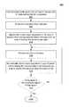
- FIG. 4is a flow diagram of an example method 400 in accordance with various embodiments of the invention for producing integrated circuits (e.g., non-volatile memory devices) that include varied silicon richness silicon nitride layers.
- integrated circuitse.g., non-volatile memory devices
- FIG. 4may include various other operations and/or variations of the operations shown by FIG. 4 .
- the sequence of the operations of flow diagram 400can be modified. It is appreciated that not all of the operations in flow diagram 400 may be performed.
- method 400can include forming a tunnel oxide layer onto (or over or above) one or more semiconductor substrates. Additionally, a desired silicon richness value can be predefined or pre-establish for a first silicon nitride layer to be deposited onto (or over or above) the tunnel oxide layer. Utilizing atomic layer deposition, a first layer of silicon nitride having the desired silicon richness value can be deposited onto (or over or above) the tunnel oxide layer. In addition, a reduction can be made to the silicon richness value. Furthermore, utilizing atomic layer deposition, an additional layer of silicon nitride having the reduced silicon richness value can be deposited onto (or over or above) the previous layer of silicon nitride.
- a tunnel oxide layer(e.g., 204 ) can be formed onto (or over or above) one or more semiconductor substrates (e.g., 102 ). It is pointed out that operation 402 can be implemented in a wide variety of ways.
- FIG. 5Ais a side sectional view of a tunnel oxide layer 504 formed onto (or over or above) a silicon wafer 502 at operation 402 .
- the forming of the tunnel oxide layer 504 onto (or over or above) the silicon wafer 502 at operation 402can be performed using atomic layer deposition, but is not limited to such.
- the tunnel oxide layer 504can be formed or deposited at any thickness at operation 402 . Note that operation 402 can be implemented in any manner similar to that described herein, but is not limited to such.
- a desired silicon richness valuecan be predefined or pre-establish for a first silicon nitride layer to be deposited onto (or over or above) the tunnel oxide layer. It is noted that the operation 404 can be implemented in a wide variety of ways. For example in one embodiment, at operation 404 a desired silicon richness value can be predefined at a silicon richness ranging from one extreme of almost 100% silicon with the remaining percentage being nitride to the other extreme of almost 100% nitride with the remaining percentage being silicon, and anywhere in between.
- a desired silicon richness valuecan be predefined at a silicon richness of k ⁇ 1.6 (wherein k is the extinction coefficient at a wavelength of 248 nm), but is not limited to such.
- the desired silicon richness valuecan be predefined at any type of silicon richness at operation 404 . It is noted that operation 404 can be implemented in any manner similar to that described herein, but is not limited to such.
- a first layer of silicon nitride (e.g., 206 ′) having the desired silicon richness valuecan be deposited onto (or over or above) the tunnel oxide layer.
- the operation 406can be implemented in a wide variety of ways.
- FIG. 5Bis a side sectional view of a first layer of silicon nitride 506 having the desired silicon richness value deposited via atomic layer deposition onto (or over or above) the tunnel oxide layer 504 at operation 406 .
- the silicon nitride layer or film 506can be deposited at any thickness at operation 406 .
- the silicon nitride layer 506can be deposited at operation 406 to have a thickness of approximately 2-10 angstroms (or approximately 0.2-1 nm), but is not limited to such. It is noted that operation 406 can be implemented in any manner similar to that described herein, but is not limited to such.
- a reductioncan be made to the silicon richness value.
- the operation 408can be implemented in a wide variety of ways.
- the silicon richness valuecan be reduced by a predefined amount, but is not limited to such.
- the silicon richness valuecan be reduced at operation 408 to have a silicon richness of k ⁇ 1.4, but is not limited to such.
- the silicon richness valuecan be reduced at operation 408 to have any type of silicon richness.
- operation 408can be implemented in any manner similar to that described herein, but is not limited to such.
- an additional layer of silicon nitride having the reduced silicon richness valuecan be deposited onto (or over or above) the previous layer of silicon nitride.
- the operation 410can be implemented in a wide variety of ways.
- FIG. 5Cis a side sectional view of an additional layer of silicon nitride 508 having the reduced silicon richness value deposited at operation 410 via atomic layer deposition onto (or over or above) the previous silicon nitride layer 506 .
- the silicon nitride film 508can be deposited at operation 410 to any thickness at operation 410 .
- the silicon nitride film 508can be deposited at operation 410 to have a thickness of approximately 2-10 angstroms (or approximately 0.2-1 nm), but is not limited to such. It is pointed out that operation 410 can be implemented in any manner similar to that described herein, but is not limited to such.
- method 400can produce integrated circuits (e.g., non-volatile memory devices) that include varied silicon richness silicon nitride layers. It is noted that method 400 may produce one or more potential benefits similar to those described herein, but is not limited to such. In addition, method 400 is not limited in any way by those potential benefits.
- integrated circuitse.g., non-volatile memory devices
- method 400may produce one or more potential benefits similar to those described herein, but is not limited to such.
- method 400is not limited in any way by those potential benefits.
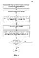
- FIG. 6is a flow diagram of an example method 600 in accordance with various embodiments of the invention for producing integrated circuits (e.g., non-volatile memory devices) that include varied silicon richness silicon nitride layers.
- integrated circuitse.g., non-volatile memory devices
- FIG. 6may not include all of the operations illustrated by FIG. 6 .
- method 600may include various other operations and/or variations of the operations shown by FIG. 6 .
- the sequence of the operations of flow diagram 600can be modified. It is appreciated that not all of the operations in flow diagram 600 may be performed.
- method 600can include forming a tunnel oxide layer onto (or over or above) one or more semiconductor substrates. Additionally, using atomic layer deposition, a first layer of silicon nitride having a first silicon richness value can be deposited onto (or over or above) the tunnel oxide layer. Furthermore, utilizing atomic layer deposition, an additional layer of silicon nitride having a different silicon richness value than the previous silicon nitride layer can be deposited onto (or over or above) the previous layer of silicon nitride. A determination can be made as to whether to deposit another silicon nitride layer. If so, process 600 can return to the operation involving the deposition of an additional silicon nitride layer. However, if it is determined that no more silicon nitride layers are to be deposited, process 600 can be ended.
- a tunnel oxide layer(e.g., 204 ) can be formed onto (or over or above) one or more semiconductor substrates (e.g., 102 ). It is pointed out that the operation 602 can be implemented in a wide variety of ways.
- FIG. 7Ais a side sectional view of a tunnel oxide layer 704 formed onto (or over or above) a semiconductor wafer 702 at operation 602 .
- the forming of the tunnel oxide layer 704 onto (or over or above) the semiconductor wafer 702 at operation 602can be performed using atomic layer deposition, but is not limited to such.
- the tunnel oxide layer 704can be formed or deposited at operation 602 to any thickness. It is noted that operation 602 can be implemented in any manner similar to that described herein, but is not limited to such.
- a first layer of silicon nitride (e.g., 206 ) having a first silicon richnesscan be deposited onto (or over or above) the tunnel oxide layer.
- the operation 604can be implemented in a wide variety of ways.
- FIG. 7Bis a side sectional view of a first layer of silicon nitride 706 having a first silicon richness deposited at operation 604 via atomic layer deposition onto (or over or above) the tunnel oxide layer 704 .
- the silicon nitride film or layer 706can have a silicon richness of k ⁇ 1.6 (wherein k is the extinction coefficient at a wavelength of 248 nm) at operation 604 , but is not limited to such.
- the silicon nitride film 706can be deposited at operation 604 via atomic layer deposition with any type of silicon richness.
- the silicon nitride film 706can be deposited at operation 604 via atomic layer deposition with a silicon richness ranging from one extreme of almost 100% silicon with the remaining percentage being nitride to the other extreme of almost 100% nitride with the remaining percentage being silicon, and anywhere in between.
- the first layer of silicon nitride 706can be deposited at operation 604 to include an upper film or layer of stoichiometric silicon nitride 714 , but is not limited to such.
- the silicon nitride film 706can be deposited at operation 604 to any thickness.
- the silicon nitride film 706can be deposited at operation 604 to have a thickness of approximately 2-10 angstroms (or approximately 0.2-1 nm), but is not limited to such.
- operation 604can be implemented in any manner similar to that described herein, but is not limited to such.
- an additional layer of silicon nitride having a different silicon richness value than the previous silicon nitride layercan be deposited onto (or over or above) the previous layer of silicon nitride.
- the operation 606can be implemented in a wide variety of ways.
- FIG. 7Cis a side sectional view of an additional layer of silicon nitride 708 having a different silicon richness value than the previous silicon nitride layer deposited at operation 606 via atomic layer deposition onto (or over or above) the previous silicon nitride layer 706 .
- the silicon nitride film or layer 708can have a silicon richness of k ⁇ 1.4 or ⁇ 1.7 at operation 606 , but is not limited to such.
- the silicon nitride film 708can be deposited at operation 606 via atomic layer deposition with a silicon richness value that is greater than or less than the silicon richness value of the previously deposited silicon nitride layer 706 .
- the additional layer of silicon nitride 708can be deposited at operation 606 to include an upper film or layer of stoichiometric silicon nitride 714 , but is not limited to such.
- the silicon nitride film 708can be deposited at operation 606 to any thickness.
- the silicon nitride film 708can be deposited at operation 606 to have a thickness of approximately 2-10 angstroms (or approximately 0.2-1 nm), but is not limited to such. It is pointed out that operation 606 can be implemented in any manner similar to that described herein, but is not limited to such.
- method 600can produce integrated circuits (e.g., non-volatile memory devices) that include varied silicon richness silicon nitride layers. Note that method 600 may produce one or more potential benefits similar to those described herein, but is not limited to such. Furthermore, method 600 is not limited in any way by those potential benefits.
Landscapes
- Engineering & Computer Science (AREA)
- Physics & Mathematics (AREA)
- Condensed Matter Physics & Semiconductors (AREA)
- General Physics & Mathematics (AREA)
- Manufacturing & Machinery (AREA)
- Computer Hardware Design (AREA)
- Microelectronics & Electronic Packaging (AREA)
- Power Engineering (AREA)
- Non-Volatile Memory (AREA)
- Semiconductor Memories (AREA)
- Chemical & Material Sciences (AREA)
- Chemical Kinetics & Catalysis (AREA)
Abstract
Description
Claims (20)
Priority Applications (5)
| Application Number | Priority Date | Filing Date | Title |
|---|---|---|---|
| US12/556,199US9012333B2 (en) | 2009-09-09 | 2009-09-09 | Varied silicon richness silicon nitride formation |
| US14/665,311US20150194499A1 (en) | 2009-09-09 | 2015-03-23 | Varied silicon richness silicon nitride formation |
| US15/690,494US10644126B2 (en) | 2009-09-09 | 2017-08-30 | Varied silicon richness silicon nitride formation |
| US16/865,980US11069789B2 (en) | 2009-09-09 | 2020-05-04 | Varied silicon richness silicon nitride formation |
| US17/376,468US20220005933A1 (en) | 2009-09-09 | 2021-07-15 | Varied silicon richness silicon nitride formation |
Applications Claiming Priority (1)
| Application Number | Priority Date | Filing Date | Title |
|---|---|---|---|
| US12/556,199US9012333B2 (en) | 2009-09-09 | 2009-09-09 | Varied silicon richness silicon nitride formation |
Related Child Applications (1)
| Application Number | Title | Priority Date | Filing Date |
|---|---|---|---|
| US14/665,311DivisionUS20150194499A1 (en) | 2009-09-09 | 2015-03-23 | Varied silicon richness silicon nitride formation |
Publications (2)
| Publication Number | Publication Date |
|---|---|
| US20110057248A1 US20110057248A1 (en) | 2011-03-10 |
| US9012333B2true US9012333B2 (en) | 2015-04-21 |
Family
ID=43647037
Family Applications (2)
| Application Number | Title | Priority Date | Filing Date |
|---|---|---|---|
| US12/556,199Active2031-11-06US9012333B2 (en) | 2009-09-09 | 2009-09-09 | Varied silicon richness silicon nitride formation |
| US14/665,311AbandonedUS20150194499A1 (en) | 2009-09-09 | 2015-03-23 | Varied silicon richness silicon nitride formation |
Family Applications After (1)
| Application Number | Title | Priority Date | Filing Date |
|---|---|---|---|
| US14/665,311AbandonedUS20150194499A1 (en) | 2009-09-09 | 2015-03-23 | Varied silicon richness silicon nitride formation |
Country Status (1)
| Country | Link |
|---|---|
| US (2) | US9012333B2 (en) |
Families Citing this family (355)
| Publication number | Priority date | Publication date | Assignee | Title |
|---|---|---|---|---|
| US10378106B2 (en) | 2008-11-14 | 2019-08-13 | Asm Ip Holding B.V. | Method of forming insulation film by modified PEALD |
| US9394608B2 (en) | 2009-04-06 | 2016-07-19 | Asm America, Inc. | Semiconductor processing reactor and components thereof |
| US8802201B2 (en) | 2009-08-14 | 2014-08-12 | Asm America, Inc. | Systems and methods for thin-film deposition of metal oxides using excited nitrogen-oxygen species |
| US10644126B2 (en) | 2009-09-09 | 2020-05-05 | Monterey Research, Llc | Varied silicon richness silicon nitride formation |
| US9312155B2 (en) | 2011-06-06 | 2016-04-12 | Asm Japan K.K. | High-throughput semiconductor-processing apparatus equipped with multiple dual-chamber modules |
| US10364496B2 (en) | 2011-06-27 | 2019-07-30 | Asm Ip Holding B.V. | Dual section module having shared and unshared mass flow controllers |
| US10854498B2 (en) | 2011-07-15 | 2020-12-01 | Asm Ip Holding B.V. | Wafer-supporting device and method for producing same |
| US20130023129A1 (en) | 2011-07-20 | 2013-01-24 | Asm America, Inc. | Pressure transmitter for a semiconductor processing environment |
| US9017481B1 (en) | 2011-10-28 | 2015-04-28 | Asm America, Inc. | Process feed management for semiconductor substrate processing |
| US9659799B2 (en) | 2012-08-28 | 2017-05-23 | Asm Ip Holding B.V. | Systems and methods for dynamic semiconductor process scheduling |
| US9021985B2 (en) | 2012-09-12 | 2015-05-05 | Asm Ip Holdings B.V. | Process gas management for an inductively-coupled plasma deposition reactor |
| US10714315B2 (en) | 2012-10-12 | 2020-07-14 | Asm Ip Holdings B.V. | Semiconductor reaction chamber showerhead |
| US20160376700A1 (en) | 2013-02-01 | 2016-12-29 | Asm Ip Holding B.V. | System for treatment of deposition reactor |
| US9589770B2 (en) | 2013-03-08 | 2017-03-07 | Asm Ip Holding B.V. | Method and systems for in-situ formation of intermediate reactive species |
| US9484191B2 (en) | 2013-03-08 | 2016-11-01 | Asm Ip Holding B.V. | Pulsed remote plasma method and system |
| US9614105B2 (en) | 2013-04-22 | 2017-04-04 | Cypress Semiconductor Corporation | Charge-trap NOR with silicon-rich nitride as a charge trap layer |
| CN104218090B (en)* | 2013-05-31 | 2017-01-04 | 上海和辉光电有限公司 | Thin film transistor (TFT) and manufacture method thereof and there is the display device of this thin film transistor (TFT) |
| US9343317B2 (en) | 2013-07-01 | 2016-05-17 | Micron Technology, Inc. | Methods of forming silicon-containing dielectric materials and semiconductor device structures |
| US9240412B2 (en) | 2013-09-27 | 2016-01-19 | Asm Ip Holding B.V. | Semiconductor structure and device and methods of forming same using selective epitaxial process |
| US10683571B2 (en) | 2014-02-25 | 2020-06-16 | Asm Ip Holding B.V. | Gas supply manifold and method of supplying gases to chamber using same |
| US10167557B2 (en) | 2014-03-18 | 2019-01-01 | Asm Ip Holding B.V. | Gas distribution system, reactor including the system, and methods of using the same |
| US11015245B2 (en) | 2014-03-19 | 2021-05-25 | Asm Ip Holding B.V. | Gas-phase reactor and system having exhaust plenum and components thereof |
| US10858737B2 (en) | 2014-07-28 | 2020-12-08 | Asm Ip Holding B.V. | Showerhead assembly and components thereof |
| US9890456B2 (en) | 2014-08-21 | 2018-02-13 | Asm Ip Holding B.V. | Method and system for in situ formation of gas-phase compounds |
| US9657845B2 (en) | 2014-10-07 | 2017-05-23 | Asm Ip Holding B.V. | Variable conductance gas distribution apparatus and method |
| US10941490B2 (en) | 2014-10-07 | 2021-03-09 | Asm Ip Holding B.V. | Multiple temperature range susceptor, assembly, reactor and system including the susceptor, and methods of using the same |
| KR102263121B1 (en) | 2014-12-22 | 2021-06-09 | 에이에스엠 아이피 홀딩 비.브이. | Semiconductor device and manufacuring method thereof |
| US10529542B2 (en) | 2015-03-11 | 2020-01-07 | Asm Ip Holdings B.V. | Cross-flow reactor and method |
| US10276355B2 (en) | 2015-03-12 | 2019-04-30 | Asm Ip Holding B.V. | Multi-zone reactor, system including the reactor, and method of using the same |
| US10458018B2 (en) | 2015-06-26 | 2019-10-29 | Asm Ip Holding B.V. | Structures including metal carbide material, devices including the structures, and methods of forming same |
| US10600673B2 (en) | 2015-07-07 | 2020-03-24 | Asm Ip Holding B.V. | Magnetic susceptor to baseplate seal |
| US9960072B2 (en) | 2015-09-29 | 2018-05-01 | Asm Ip Holding B.V. | Variable adjustment for precise matching of multiple chamber cavity housings |
| US10211308B2 (en) | 2015-10-21 | 2019-02-19 | Asm Ip Holding B.V. | NbMC layers |
| US10322384B2 (en) | 2015-11-09 | 2019-06-18 | Asm Ip Holding B.V. | Counter flow mixer for process chamber |
| US11139308B2 (en) | 2015-12-29 | 2021-10-05 | Asm Ip Holding B.V. | Atomic layer deposition of III-V compounds to form V-NAND devices |
| US10529554B2 (en) | 2016-02-19 | 2020-01-07 | Asm Ip Holding B.V. | Method for forming silicon nitride film selectively on sidewalls or flat surfaces of trenches |
| US10468251B2 (en) | 2016-02-19 | 2019-11-05 | Asm Ip Holding B.V. | Method for forming spacers using silicon nitride film for spacer-defined multiple patterning |
| US10501866B2 (en) | 2016-03-09 | 2019-12-10 | Asm Ip Holding B.V. | Gas distribution apparatus for improved film uniformity in an epitaxial system |
| US10343920B2 (en) | 2016-03-18 | 2019-07-09 | Asm Ip Holding B.V. | Aligned carbon nanotubes |
| US9892913B2 (en) | 2016-03-24 | 2018-02-13 | Asm Ip Holding B.V. | Radial and thickness control via biased multi-port injection settings |
| US10190213B2 (en) | 2016-04-21 | 2019-01-29 | Asm Ip Holding B.V. | Deposition of metal borides |
| US10865475B2 (en) | 2016-04-21 | 2020-12-15 | Asm Ip Holding B.V. | Deposition of metal borides and silicides |
| US10367080B2 (en)* | 2016-05-02 | 2019-07-30 | Asm Ip Holding B.V. | Method of forming a germanium oxynitride film |
| US10032628B2 (en) | 2016-05-02 | 2018-07-24 | Asm Ip Holding B.V. | Source/drain performance through conformal solid state doping |
| KR102592471B1 (en) | 2016-05-17 | 2023-10-20 | 에이에스엠 아이피 홀딩 비.브이. | Method of forming metal interconnection and method of fabricating semiconductor device using the same |
| US11453943B2 (en) | 2016-05-25 | 2022-09-27 | Asm Ip Holding B.V. | Method for forming carbon-containing silicon/metal oxide or nitride film by ALD using silicon precursor and hydrocarbon precursor |
| US10388509B2 (en) | 2016-06-28 | 2019-08-20 | Asm Ip Holding B.V. | Formation of epitaxial layers via dislocation filtering |
| US10612137B2 (en) | 2016-07-08 | 2020-04-07 | Asm Ip Holdings B.V. | Organic reactants for atomic layer deposition |
| US9859151B1 (en) | 2016-07-08 | 2018-01-02 | Asm Ip Holding B.V. | Selective film deposition method to form air gaps |
| US10714385B2 (en) | 2016-07-19 | 2020-07-14 | Asm Ip Holding B.V. | Selective deposition of tungsten |
| KR102354490B1 (en) | 2016-07-27 | 2022-01-21 | 에이에스엠 아이피 홀딩 비.브이. | Method of processing a substrate |
| US9887082B1 (en) | 2016-07-28 | 2018-02-06 | Asm Ip Holding B.V. | Method and apparatus for filling a gap |
| US10395919B2 (en) | 2016-07-28 | 2019-08-27 | Asm Ip Holding B.V. | Method and apparatus for filling a gap |
| KR102532607B1 (en) | 2016-07-28 | 2023-05-15 | 에이에스엠 아이피 홀딩 비.브이. | Substrate processing apparatus and method of operating the same |
| US9812320B1 (en) | 2016-07-28 | 2017-11-07 | Asm Ip Holding B.V. | Method and apparatus for filling a gap |
| US10410943B2 (en) | 2016-10-13 | 2019-09-10 | Asm Ip Holding B.V. | Method for passivating a surface of a semiconductor and related systems |
| US10643826B2 (en) | 2016-10-26 | 2020-05-05 | Asm Ip Holdings B.V. | Methods for thermally calibrating reaction chambers |
| US11532757B2 (en) | 2016-10-27 | 2022-12-20 | Asm Ip Holding B.V. | Deposition of charge trapping layers |
| US10643904B2 (en) | 2016-11-01 | 2020-05-05 | Asm Ip Holdings B.V. | Methods for forming a semiconductor device and related semiconductor device structures |
| US10435790B2 (en) | 2016-11-01 | 2019-10-08 | Asm Ip Holding B.V. | Method of subatmospheric plasma-enhanced ALD using capacitively coupled electrodes with narrow gap |
| US10229833B2 (en) | 2016-11-01 | 2019-03-12 | Asm Ip Holding B.V. | Methods for forming a transition metal nitride film on a substrate by atomic layer deposition and related semiconductor device structures |
| US10714350B2 (en) | 2016-11-01 | 2020-07-14 | ASM IP Holdings, B.V. | Methods for forming a transition metal niobium nitride film on a substrate by atomic layer deposition and related semiconductor device structures |
| US10134757B2 (en) | 2016-11-07 | 2018-11-20 | Asm Ip Holding B.V. | Method of processing a substrate and a device manufactured by using the method |
| KR102546317B1 (en) | 2016-11-15 | 2023-06-21 | 에이에스엠 아이피 홀딩 비.브이. | Gas supply unit and substrate processing apparatus including the same |
| US10340135B2 (en) | 2016-11-28 | 2019-07-02 | Asm Ip Holding B.V. | Method of topologically restricted plasma-enhanced cyclic deposition of silicon or metal nitride |
| KR102762543B1 (en) | 2016-12-14 | 2025-02-05 | 에이에스엠 아이피 홀딩 비.브이. | Substrate processing apparatus |
| US11581186B2 (en) | 2016-12-15 | 2023-02-14 | Asm Ip Holding B.V. | Sequential infiltration synthesis apparatus |
| US11447861B2 (en) | 2016-12-15 | 2022-09-20 | Asm Ip Holding B.V. | Sequential infiltration synthesis apparatus and a method of forming a patterned structure |
| KR102700194B1 (en) | 2016-12-19 | 2024-08-28 | 에이에스엠 아이피 홀딩 비.브이. | Substrate processing apparatus |
| US10269558B2 (en) | 2016-12-22 | 2019-04-23 | Asm Ip Holding B.V. | Method of forming a structure on a substrate |
| US10867788B2 (en) | 2016-12-28 | 2020-12-15 | Asm Ip Holding B.V. | Method of forming a structure on a substrate |
| US11390950B2 (en) | 2017-01-10 | 2022-07-19 | Asm Ip Holding B.V. | Reactor system and method to reduce residue buildup during a film deposition process |
| US10655221B2 (en) | 2017-02-09 | 2020-05-19 | Asm Ip Holding B.V. | Method for depositing oxide film by thermal ALD and PEALD |
| US10468261B2 (en) | 2017-02-15 | 2019-11-05 | Asm Ip Holding B.V. | Methods for forming a metallic film on a substrate by cyclical deposition and related semiconductor device structures |
| US10529563B2 (en) | 2017-03-29 | 2020-01-07 | Asm Ip Holdings B.V. | Method for forming doped metal oxide films on a substrate by cyclical deposition and related semiconductor device structures |
| US10283353B2 (en) | 2017-03-29 | 2019-05-07 | Asm Ip Holding B.V. | Method of reforming insulating film deposited on substrate with recess pattern |
| KR102457289B1 (en) | 2017-04-25 | 2022-10-21 | 에이에스엠 아이피 홀딩 비.브이. | Method for depositing a thin film and manufacturing a semiconductor device |
| US10770286B2 (en) | 2017-05-08 | 2020-09-08 | Asm Ip Holdings B.V. | Methods for selectively forming a silicon nitride film on a substrate and related semiconductor device structures |
| US10892156B2 (en) | 2017-05-08 | 2021-01-12 | Asm Ip Holding B.V. | Methods for forming a silicon nitride film on a substrate and related semiconductor device structures |
| US10446393B2 (en) | 2017-05-08 | 2019-10-15 | Asm Ip Holding B.V. | Methods for forming silicon-containing epitaxial layers and related semiconductor device structures |
| US10504742B2 (en) | 2017-05-31 | 2019-12-10 | Asm Ip Holding B.V. | Method of atomic layer etching using hydrogen plasma |
| US10886123B2 (en) | 2017-06-02 | 2021-01-05 | Asm Ip Holding B.V. | Methods for forming low temperature semiconductor layers and related semiconductor device structures |
| US12040200B2 (en) | 2017-06-20 | 2024-07-16 | Asm Ip Holding B.V. | Semiconductor processing apparatus and methods for calibrating a semiconductor processing apparatus |
| US11306395B2 (en) | 2017-06-28 | 2022-04-19 | Asm Ip Holding B.V. | Methods for depositing a transition metal nitride film on a substrate by atomic layer deposition and related deposition apparatus |
| US10685834B2 (en) | 2017-07-05 | 2020-06-16 | Asm Ip Holdings B.V. | Methods for forming a silicon germanium tin layer and related semiconductor device structures |
| KR20190009245A (en) | 2017-07-18 | 2019-01-28 | 에이에스엠 아이피 홀딩 비.브이. | Methods for forming a semiconductor device structure and related semiconductor device structures |
| US10541333B2 (en) | 2017-07-19 | 2020-01-21 | Asm Ip Holding B.V. | Method for depositing a group IV semiconductor and related semiconductor device structures |
| US11374112B2 (en) | 2017-07-19 | 2022-06-28 | Asm Ip Holding B.V. | Method for depositing a group IV semiconductor and related semiconductor device structures |
| US11018002B2 (en) | 2017-07-19 | 2021-05-25 | Asm Ip Holding B.V. | Method for selectively depositing a Group IV semiconductor and related semiconductor device structures |
| US10605530B2 (en) | 2017-07-26 | 2020-03-31 | Asm Ip Holding B.V. | Assembly of a liner and a flange for a vertical furnace as well as the liner and the vertical furnace |
| US10590535B2 (en) | 2017-07-26 | 2020-03-17 | Asm Ip Holdings B.V. | Chemical treatment, deposition and/or infiltration apparatus and method for using the same |
| US10312055B2 (en) | 2017-07-26 | 2019-06-04 | Asm Ip Holding B.V. | Method of depositing film by PEALD using negative bias |
| TWI815813B (en) | 2017-08-04 | 2023-09-21 | 荷蘭商Asm智慧財產控股公司 | Showerhead assembly for distributing a gas within a reaction chamber |
| US10692741B2 (en) | 2017-08-08 | 2020-06-23 | Asm Ip Holdings B.V. | Radiation shield |
| US10770336B2 (en) | 2017-08-08 | 2020-09-08 | Asm Ip Holding B.V. | Substrate lift mechanism and reactor including same |
| US11769682B2 (en) | 2017-08-09 | 2023-09-26 | Asm Ip Holding B.V. | Storage apparatus for storing cassettes for substrates and processing apparatus equipped therewith |
| US10249524B2 (en) | 2017-08-09 | 2019-04-02 | Asm Ip Holding B.V. | Cassette holder assembly for a substrate cassette and holding member for use in such assembly |
| US11139191B2 (en) | 2017-08-09 | 2021-10-05 | Asm Ip Holding B.V. | Storage apparatus for storing cassettes for substrates and processing apparatus equipped therewith |
| US10236177B1 (en) | 2017-08-22 | 2019-03-19 | ASM IP Holding B.V.. | Methods for depositing a doped germanium tin semiconductor and related semiconductor device structures |
| USD900036S1 (en) | 2017-08-24 | 2020-10-27 | Asm Ip Holding B.V. | Heater electrical connector and adapter |
| US11830730B2 (en) | 2017-08-29 | 2023-11-28 | Asm Ip Holding B.V. | Layer forming method and apparatus |
| KR102491945B1 (en) | 2017-08-30 | 2023-01-26 | 에이에스엠 아이피 홀딩 비.브이. | Substrate processing apparatus |
| US11295980B2 (en) | 2017-08-30 | 2022-04-05 | Asm Ip Holding B.V. | Methods for depositing a molybdenum metal film over a dielectric surface of a substrate by a cyclical deposition process and related semiconductor device structures |
| US11056344B2 (en) | 2017-08-30 | 2021-07-06 | Asm Ip Holding B.V. | Layer forming method |
| KR102401446B1 (en) | 2017-08-31 | 2022-05-24 | 에이에스엠 아이피 홀딩 비.브이. | Substrate processing apparatus |
| US10607895B2 (en) | 2017-09-18 | 2020-03-31 | Asm Ip Holdings B.V. | Method for forming a semiconductor device structure comprising a gate fill metal |
| KR102630301B1 (en) | 2017-09-21 | 2024-01-29 | 에이에스엠 아이피 홀딩 비.브이. | Method of sequential infiltration synthesis treatment of infiltrateable material and structures and devices formed using same |
| US10844484B2 (en) | 2017-09-22 | 2020-11-24 | Asm Ip Holding B.V. | Apparatus for dispensing a vapor phase reactant to a reaction chamber and related methods |
| US10658205B2 (en) | 2017-09-28 | 2020-05-19 | Asm Ip Holdings B.V. | Chemical dispensing apparatus and methods for dispensing a chemical to a reaction chamber |
| US10403504B2 (en) | 2017-10-05 | 2019-09-03 | Asm Ip Holding B.V. | Method for selectively depositing a metallic film on a substrate |
| US10319588B2 (en) | 2017-10-10 | 2019-06-11 | Asm Ip Holding B.V. | Method for depositing a metal chalcogenide on a substrate by cyclical deposition |
| US10923344B2 (en) | 2017-10-30 | 2021-02-16 | Asm Ip Holding B.V. | Methods for forming a semiconductor structure and related semiconductor structures |
| KR102443047B1 (en) | 2017-11-16 | 2022-09-14 | 에이에스엠 아이피 홀딩 비.브이. | Method of processing a substrate and a device manufactured by the same |
| US10910262B2 (en) | 2017-11-16 | 2021-02-02 | Asm Ip Holding B.V. | Method of selectively depositing a capping layer structure on a semiconductor device structure |
| US11022879B2 (en) | 2017-11-24 | 2021-06-01 | Asm Ip Holding B.V. | Method of forming an enhanced unexposed photoresist layer |
| CN111344522B (en) | 2017-11-27 | 2022-04-12 | 阿斯莫Ip控股公司 | Including clean mini-environment device |
| WO2019103613A1 (en) | 2017-11-27 | 2019-05-31 | Asm Ip Holding B.V. | A storage device for storing wafer cassettes for use with a batch furnace |
| US10290508B1 (en) | 2017-12-05 | 2019-05-14 | Asm Ip Holding B.V. | Method for forming vertical spacers for spacer-defined patterning |
| US10872771B2 (en) | 2018-01-16 | 2020-12-22 | Asm Ip Holding B. V. | Method for depositing a material film on a substrate within a reaction chamber by a cyclical deposition process and related device structures |
| TWI799494B (en) | 2018-01-19 | 2023-04-21 | 荷蘭商Asm 智慧財產控股公司 | Deposition method |
| KR102695659B1 (en) | 2018-01-19 | 2024-08-14 | 에이에스엠 아이피 홀딩 비.브이. | Method for depositing a gap filling layer by plasma assisted deposition |
| USD903477S1 (en) | 2018-01-24 | 2020-12-01 | Asm Ip Holdings B.V. | Metal clamp |
| US11018047B2 (en) | 2018-01-25 | 2021-05-25 | Asm Ip Holding B.V. | Hybrid lift pin |
| USD880437S1 (en) | 2018-02-01 | 2020-04-07 | Asm Ip Holding B.V. | Gas supply plate for semiconductor manufacturing apparatus |
| US10535516B2 (en) | 2018-02-01 | 2020-01-14 | Asm Ip Holdings B.V. | Method for depositing a semiconductor structure on a surface of a substrate and related semiconductor structures |
| US11081345B2 (en) | 2018-02-06 | 2021-08-03 | Asm Ip Holding B.V. | Method of post-deposition treatment for silicon oxide film |
| WO2019158960A1 (en) | 2018-02-14 | 2019-08-22 | Asm Ip Holding B.V. | A method for depositing a ruthenium-containing film on a substrate by a cyclical deposition process |
| US10896820B2 (en) | 2018-02-14 | 2021-01-19 | Asm Ip Holding B.V. | Method for depositing a ruthenium-containing film on a substrate by a cyclical deposition process |
| US10731249B2 (en) | 2018-02-15 | 2020-08-04 | Asm Ip Holding B.V. | Method of forming a transition metal containing film on a substrate by a cyclical deposition process, a method for supplying a transition metal halide compound to a reaction chamber, and related vapor deposition apparatus |
| KR102636427B1 (en) | 2018-02-20 | 2024-02-13 | 에이에스엠 아이피 홀딩 비.브이. | Substrate processing method and apparatus |
| US10658181B2 (en) | 2018-02-20 | 2020-05-19 | Asm Ip Holding B.V. | Method of spacer-defined direct patterning in semiconductor fabrication |
| US10975470B2 (en) | 2018-02-23 | 2021-04-13 | Asm Ip Holding B.V. | Apparatus for detecting or monitoring for a chemical precursor in a high temperature environment |
| US11473195B2 (en) | 2018-03-01 | 2022-10-18 | Asm Ip Holding B.V. | Semiconductor processing apparatus and a method for processing a substrate |
| US11629406B2 (en) | 2018-03-09 | 2023-04-18 | Asm Ip Holding B.V. | Semiconductor processing apparatus comprising one or more pyrometers for measuring a temperature of a substrate during transfer of the substrate |
| US11114283B2 (en) | 2018-03-16 | 2021-09-07 | Asm Ip Holding B.V. | Reactor, system including the reactor, and methods of manufacturing and using same |
| KR102646467B1 (en) | 2018-03-27 | 2024-03-11 | 에이에스엠 아이피 홀딩 비.브이. | Method of forming an electrode on a substrate and a semiconductor device structure including an electrode |
| US11088002B2 (en) | 2018-03-29 | 2021-08-10 | Asm Ip Holding B.V. | Substrate rack and a substrate processing system and method |
| US10510536B2 (en) | 2018-03-29 | 2019-12-17 | Asm Ip Holding B.V. | Method of depositing a co-doped polysilicon film on a surface of a substrate within a reaction chamber |
| US11230766B2 (en) | 2018-03-29 | 2022-01-25 | Asm Ip Holding B.V. | Substrate processing apparatus and method |
| KR102501472B1 (en) | 2018-03-30 | 2023-02-20 | 에이에스엠 아이피 홀딩 비.브이. | Substrate processing method |
| KR102600229B1 (en) | 2018-04-09 | 2023-11-10 | 에이에스엠 아이피 홀딩 비.브이. | Substrate supporting device, substrate processing apparatus including the same and substrate processing method |
| US12025484B2 (en) | 2018-05-08 | 2024-07-02 | Asm Ip Holding B.V. | Thin film forming method |
| TWI811348B (en) | 2018-05-08 | 2023-08-11 | 荷蘭商Asm 智慧財產控股公司 | Methods for depositing an oxide film on a substrate by a cyclical deposition process and related device structures |
| US12272527B2 (en) | 2018-05-09 | 2025-04-08 | Asm Ip Holding B.V. | Apparatus for use with hydrogen radicals and method of using same |
| KR20190129718A (en) | 2018-05-11 | 2019-11-20 | 에이에스엠 아이피 홀딩 비.브이. | Methods for forming a doped metal carbide film on a substrate and related semiconductor device structures |
| KR102596988B1 (en) | 2018-05-28 | 2023-10-31 | 에이에스엠 아이피 홀딩 비.브이. | Method of processing a substrate and a device manufactured by the same |
| US11718913B2 (en) | 2018-06-04 | 2023-08-08 | Asm Ip Holding B.V. | Gas distribution system and reactor system including same |
| TWI840362B (en) | 2018-06-04 | 2024-05-01 | 荷蘭商Asm Ip私人控股有限公司 | Wafer handling chamber with moisture reduction |
| US11286562B2 (en) | 2018-06-08 | 2022-03-29 | Asm Ip Holding B.V. | Gas-phase chemical reactor and method of using same |
| US10797133B2 (en) | 2018-06-21 | 2020-10-06 | Asm Ip Holding B.V. | Method for depositing a phosphorus doped silicon arsenide film and related semiconductor device structures |
| KR102568797B1 (en) | 2018-06-21 | 2023-08-21 | 에이에스엠 아이피 홀딩 비.브이. | Substrate processing system |
| TWI873894B (en) | 2018-06-27 | 2025-02-21 | 荷蘭商Asm Ip私人控股有限公司 | Cyclic deposition methods for forming metal-containing material and films and structures including the metal-containing material |
| KR102854019B1 (en) | 2018-06-27 | 2025-09-02 | 에이에스엠 아이피 홀딩 비.브이. | Periodic deposition method for forming a metal-containing material and films and structures comprising the metal-containing material |
| US10612136B2 (en) | 2018-06-29 | 2020-04-07 | ASM IP Holding, B.V. | Temperature-controlled flange and reactor system including same |
| KR102686758B1 (en) | 2018-06-29 | 2024-07-18 | 에이에스엠 아이피 홀딩 비.브이. | Method for depositing a thin film and manufacturing a semiconductor device |
| US10755922B2 (en) | 2018-07-03 | 2020-08-25 | Asm Ip Holding B.V. | Method for depositing silicon-free carbon-containing film as gap-fill layer by pulse plasma-assisted deposition |
| US10388513B1 (en) | 2018-07-03 | 2019-08-20 | Asm Ip Holding B.V. | Method for depositing silicon-free carbon-containing film as gap-fill layer by pulse plasma-assisted deposition |
| US10767789B2 (en) | 2018-07-16 | 2020-09-08 | Asm Ip Holding B.V. | Diaphragm valves, valve components, and methods for forming valve components |
| US10483099B1 (en) | 2018-07-26 | 2019-11-19 | Asm Ip Holding B.V. | Method for forming thermally stable organosilicon polymer film |
| US11053591B2 (en) | 2018-08-06 | 2021-07-06 | Asm Ip Holding B.V. | Multi-port gas injection system and reactor system including same |
| US10883175B2 (en) | 2018-08-09 | 2021-01-05 | Asm Ip Holding B.V. | Vertical furnace for processing substrates and a liner for use therein |
| US10829852B2 (en) | 2018-08-16 | 2020-11-10 | Asm Ip Holding B.V. | Gas distribution device for a wafer processing apparatus |
| US11430674B2 (en) | 2018-08-22 | 2022-08-30 | Asm Ip Holding B.V. | Sensor array, apparatus for dispensing a vapor phase reactant to a reaction chamber and related methods |
| US11024523B2 (en) | 2018-09-11 | 2021-06-01 | Asm Ip Holding B.V. | Substrate processing apparatus and method |
| KR102707956B1 (en) | 2018-09-11 | 2024-09-19 | 에이에스엠 아이피 홀딩 비.브이. | Method for deposition of a thin film |
| US11049751B2 (en) | 2018-09-14 | 2021-06-29 | Asm Ip Holding B.V. | Cassette supply system to store and handle cassettes and processing apparatus equipped therewith |
| CN110970344B (en) | 2018-10-01 | 2024-10-25 | Asmip控股有限公司 | Substrate holding apparatus, system comprising the same and method of using the same |
| US11232963B2 (en) | 2018-10-03 | 2022-01-25 | Asm Ip Holding B.V. | Substrate processing apparatus and method |
| KR102592699B1 (en) | 2018-10-08 | 2023-10-23 | 에이에스엠 아이피 홀딩 비.브이. | Substrate support unit and apparatuses for depositing thin film and processing the substrate including the same |
| US10847365B2 (en) | 2018-10-11 | 2020-11-24 | Asm Ip Holding B.V. | Method of forming conformal silicon carbide film by cyclic CVD |
| US10811256B2 (en) | 2018-10-16 | 2020-10-20 | Asm Ip Holding B.V. | Method for etching a carbon-containing feature |
| KR102605121B1 (en) | 2018-10-19 | 2023-11-23 | 에이에스엠 아이피 홀딩 비.브이. | Substrate processing apparatus and substrate processing method |
| KR102546322B1 (en) | 2018-10-19 | 2023-06-21 | 에이에스엠 아이피 홀딩 비.브이. | Substrate processing apparatus and substrate processing method |
| USD948463S1 (en) | 2018-10-24 | 2022-04-12 | Asm Ip Holding B.V. | Susceptor for semiconductor substrate supporting apparatus |
| US10381219B1 (en) | 2018-10-25 | 2019-08-13 | Asm Ip Holding B.V. | Methods for forming a silicon nitride film |
| US12378665B2 (en) | 2018-10-26 | 2025-08-05 | Asm Ip Holding B.V. | High temperature coatings for a preclean and etch apparatus and related methods |
| US11087997B2 (en) | 2018-10-31 | 2021-08-10 | Asm Ip Holding B.V. | Substrate processing apparatus for processing substrates |
| KR102748291B1 (en) | 2018-11-02 | 2024-12-31 | 에이에스엠 아이피 홀딩 비.브이. | Substrate support unit and substrate processing apparatus including the same |
| US11572620B2 (en) | 2018-11-06 | 2023-02-07 | Asm Ip Holding B.V. | Methods for selectively depositing an amorphous silicon film on a substrate |
| US11031242B2 (en) | 2018-11-07 | 2021-06-08 | Asm Ip Holding B.V. | Methods for depositing a boron doped silicon germanium film |
| US10847366B2 (en) | 2018-11-16 | 2020-11-24 | Asm Ip Holding B.V. | Methods for depositing a transition metal chalcogenide film on a substrate by a cyclical deposition process |
| US10818758B2 (en) | 2018-11-16 | 2020-10-27 | Asm Ip Holding B.V. | Methods for forming a metal silicate film on a substrate in a reaction chamber and related semiconductor device structures |
| US10559458B1 (en) | 2018-11-26 | 2020-02-11 | Asm Ip Holding B.V. | Method of forming oxynitride film |
| US12040199B2 (en) | 2018-11-28 | 2024-07-16 | Asm Ip Holding B.V. | Substrate processing apparatus for processing substrates |
| US11217444B2 (en) | 2018-11-30 | 2022-01-04 | Asm Ip Holding B.V. | Method for forming an ultraviolet radiation responsive metal oxide-containing film |
| KR102636428B1 (en) | 2018-12-04 | 2024-02-13 | 에이에스엠 아이피 홀딩 비.브이. | A method for cleaning a substrate processing apparatus |
| US11158513B2 (en) | 2018-12-13 | 2021-10-26 | Asm Ip Holding B.V. | Methods for forming a rhenium-containing film on a substrate by a cyclical deposition process and related semiconductor device structures |
| TWI874340B (en) | 2018-12-14 | 2025-03-01 | 荷蘭商Asm Ip私人控股有限公司 | Method of forming device structure, structure formed by the method and system for performing the method |
| TWI866480B (en) | 2019-01-17 | 2024-12-11 | 荷蘭商Asm Ip 私人控股有限公司 | Methods of forming a transition metal containing film on a substrate by a cyclical deposition process |
| KR102727227B1 (en) | 2019-01-22 | 2024-11-07 | 에이에스엠 아이피 홀딩 비.브이. | Semiconductor processing device |
| CN111524788B (en) | 2019-02-01 | 2023-11-24 | Asm Ip私人控股有限公司 | Method for forming topologically selective films of silicon oxide |
| TWI873122B (en) | 2019-02-20 | 2025-02-21 | 荷蘭商Asm Ip私人控股有限公司 | Method of filling a recess formed within a surface of a substrate, semiconductor structure formed according to the method, and semiconductor processing apparatus |
| TWI845607B (en) | 2019-02-20 | 2024-06-21 | 荷蘭商Asm Ip私人控股有限公司 | Cyclical deposition method and apparatus for filling a recess formed within a substrate surface |
| KR102626263B1 (en) | 2019-02-20 | 2024-01-16 | 에이에스엠 아이피 홀딩 비.브이. | Cyclical deposition method including treatment step and apparatus for same |
| TWI838458B (en) | 2019-02-20 | 2024-04-11 | 荷蘭商Asm Ip私人控股有限公司 | Apparatus and methods for plug fill deposition in 3-d nand applications |
| TWI842826B (en) | 2019-02-22 | 2024-05-21 | 荷蘭商Asm Ip私人控股有限公司 | Substrate processing apparatus and method for processing substrate |
| KR102782593B1 (en) | 2019-03-08 | 2025-03-14 | 에이에스엠 아이피 홀딩 비.브이. | Structure Including SiOC Layer and Method of Forming Same |
| US11742198B2 (en) | 2019-03-08 | 2023-08-29 | Asm Ip Holding B.V. | Structure including SiOCN layer and method of forming same |
| KR102858005B1 (en) | 2019-03-08 | 2025-09-09 | 에이에스엠 아이피 홀딩 비.브이. | Method for Selective Deposition of Silicon Nitride Layer and Structure Including Selectively-Deposited Silicon Nitride Layer |
| JP2020167398A (en) | 2019-03-28 | 2020-10-08 | エーエスエム・アイピー・ホールディング・ベー・フェー | Door openers and substrate processing equipment provided with door openers |
| KR102809999B1 (en) | 2019-04-01 | 2025-05-19 | 에이에스엠 아이피 홀딩 비.브이. | Method of manufacturing semiconductor device |
| KR20200123380A (en) | 2019-04-19 | 2020-10-29 | 에이에스엠 아이피 홀딩 비.브이. | Layer forming method and apparatus |
| KR20200125453A (en) | 2019-04-24 | 2020-11-04 | 에이에스엠 아이피 홀딩 비.브이. | Gas-phase reactor system and method of using same |
| US11289326B2 (en) | 2019-05-07 | 2022-03-29 | Asm Ip Holding B.V. | Method for reforming amorphous carbon polymer film |
| KR20200130121A (en) | 2019-05-07 | 2020-11-18 | 에이에스엠 아이피 홀딩 비.브이. | Chemical source vessel with dip tube |
| KR20200130652A (en) | 2019-05-10 | 2020-11-19 | 에이에스엠 아이피 홀딩 비.브이. | Method of depositing material onto a surface and structure formed according to the method |
| JP7612342B2 (en) | 2019-05-16 | 2025-01-14 | エーエスエム・アイピー・ホールディング・ベー・フェー | Wafer boat handling apparatus, vertical batch furnace and method |
| JP7598201B2 (en) | 2019-05-16 | 2024-12-11 | エーエスエム・アイピー・ホールディング・ベー・フェー | Wafer boat handling apparatus, vertical batch furnace and method |
| USD975665S1 (en) | 2019-05-17 | 2023-01-17 | Asm Ip Holding B.V. | Susceptor shaft |
| USD947913S1 (en) | 2019-05-17 | 2022-04-05 | Asm Ip Holding B.V. | Susceptor shaft |
| USD935572S1 (en) | 2019-05-24 | 2021-11-09 | Asm Ip Holding B.V. | Gas channel plate |
| USD922229S1 (en) | 2019-06-05 | 2021-06-15 | Asm Ip Holding B.V. | Device for controlling a temperature of a gas supply unit |
| KR20200141002A (en) | 2019-06-06 | 2020-12-17 | 에이에스엠 아이피 홀딩 비.브이. | Method of using a gas-phase reactor system including analyzing exhausted gas |
| KR20200141931A (en) | 2019-06-10 | 2020-12-21 | 에이에스엠 아이피 홀딩 비.브이. | Method for cleaning quartz epitaxial chambers |
| KR20200143254A (en) | 2019-06-11 | 2020-12-23 | 에이에스엠 아이피 홀딩 비.브이. | Method of forming an electronic structure using an reforming gas, system for performing the method, and structure formed using the method |
| USD944946S1 (en) | 2019-06-14 | 2022-03-01 | Asm Ip Holding B.V. | Shower plate |
| USD931978S1 (en) | 2019-06-27 | 2021-09-28 | Asm Ip Holding B.V. | Showerhead vacuum transport |
| KR20210005515A (en) | 2019-07-03 | 2021-01-14 | 에이에스엠 아이피 홀딩 비.브이. | Temperature control assembly for substrate processing apparatus and method of using same |
| JP7499079B2 (en) | 2019-07-09 | 2024-06-13 | エーエスエム・アイピー・ホールディング・ベー・フェー | Plasma device using coaxial waveguide and substrate processing method |
| CN112216646A (en) | 2019-07-10 | 2021-01-12 | Asm Ip私人控股有限公司 | Substrate supporting assembly and substrate processing device comprising same |
| KR20210010307A (en) | 2019-07-16 | 2021-01-27 | 에이에스엠 아이피 홀딩 비.브이. | Substrate processing apparatus |
| KR20210010816A (en) | 2019-07-17 | 2021-01-28 | 에이에스엠 아이피 홀딩 비.브이. | Radical assist ignition plasma system and method |
| KR102860110B1 (en) | 2019-07-17 | 2025-09-16 | 에이에스엠 아이피 홀딩 비.브이. | Methods of forming silicon germanium structures |
| US11643724B2 (en) | 2019-07-18 | 2023-05-09 | Asm Ip Holding B.V. | Method of forming structures using a neutral beam |
| KR20210010817A (en) | 2019-07-19 | 2021-01-28 | 에이에스엠 아이피 홀딩 비.브이. | Method of Forming Topology-Controlled Amorphous Carbon Polymer Film |
| TWI839544B (en) | 2019-07-19 | 2024-04-21 | 荷蘭商Asm Ip私人控股有限公司 | Method of forming topology-controlled amorphous carbon polymer film |
| TWI851767B (en) | 2019-07-29 | 2024-08-11 | 荷蘭商Asm Ip私人控股有限公司 | Methods for selective deposition utilizing n-type dopants and/or alternative dopants to achieve high dopant incorporation |
| CN112309900A (en) | 2019-07-30 | 2021-02-02 | Asm Ip私人控股有限公司 | Substrate processing apparatus |
| CN112309899A (en) | 2019-07-30 | 2021-02-02 | Asm Ip私人控股有限公司 | Substrate processing apparatus |
| US12169361B2 (en) | 2019-07-30 | 2024-12-17 | Asm Ip Holding B.V. | Substrate processing apparatus and method |
| US11587815B2 (en) | 2019-07-31 | 2023-02-21 | Asm Ip Holding B.V. | Vertical batch furnace assembly |
| US11227782B2 (en) | 2019-07-31 | 2022-01-18 | Asm Ip Holding B.V. | Vertical batch furnace assembly |
| US11587814B2 (en) | 2019-07-31 | 2023-02-21 | Asm Ip Holding B.V. | Vertical batch furnace assembly |
| CN112323048B (en) | 2019-08-05 | 2024-02-09 | Asm Ip私人控股有限公司 | Liquid level sensor for chemical source container |
| CN112342526A (en) | 2019-08-09 | 2021-02-09 | Asm Ip私人控股有限公司 | Heater assembly including cooling device and method of using same |
| USD965044S1 (en) | 2019-08-19 | 2022-09-27 | Asm Ip Holding B.V. | Susceptor shaft |
| USD965524S1 (en) | 2019-08-19 | 2022-10-04 | Asm Ip Holding B.V. | Susceptor support |
| JP2021031769A (en) | 2019-08-21 | 2021-03-01 | エーエスエム アイピー ホールディング ビー.ブイ. | Production apparatus of mixed gas of film deposition raw material and film deposition apparatus |
| USD979506S1 (en) | 2019-08-22 | 2023-02-28 | Asm Ip Holding B.V. | Insulator |
| USD949319S1 (en) | 2019-08-22 | 2022-04-19 | Asm Ip Holding B.V. | Exhaust duct |
| USD930782S1 (en) | 2019-08-22 | 2021-09-14 | Asm Ip Holding B.V. | Gas distributor |
| KR20210024423A (en) | 2019-08-22 | 2021-03-05 | 에이에스엠 아이피 홀딩 비.브이. | Method for forming a structure with a hole |
| USD940837S1 (en) | 2019-08-22 | 2022-01-11 | Asm Ip Holding B.V. | Electrode |
| KR20210024420A (en) | 2019-08-23 | 2021-03-05 | 에이에스엠 아이피 홀딩 비.브이. | Method for depositing silicon oxide film having improved quality by peald using bis(diethylamino)silane |
| US11286558B2 (en) | 2019-08-23 | 2022-03-29 | Asm Ip Holding B.V. | Methods for depositing a molybdenum nitride film on a surface of a substrate by a cyclical deposition process and related semiconductor device structures including a molybdenum nitride film |
| KR102806450B1 (en) | 2019-09-04 | 2025-05-12 | 에이에스엠 아이피 홀딩 비.브이. | Methods for selective deposition using a sacrificial capping layer |
| KR102733104B1 (en) | 2019-09-05 | 2024-11-22 | 에이에스엠 아이피 홀딩 비.브이. | Substrate processing apparatus |
| US11562901B2 (en) | 2019-09-25 | 2023-01-24 | Asm Ip Holding B.V. | Substrate processing method |
| CN112593212B (en) | 2019-10-02 | 2023-12-22 | Asm Ip私人控股有限公司 | Method for forming topologically selective silicon oxide film by cyclic plasma enhanced deposition process |
| KR20210042810A (en) | 2019-10-08 | 2021-04-20 | 에이에스엠 아이피 홀딩 비.브이. | Reactor system including a gas distribution assembly for use with activated species and method of using same |
| TWI846953B (en) | 2019-10-08 | 2024-07-01 | 荷蘭商Asm Ip私人控股有限公司 | Substrate processing device |
| TW202128273A (en) | 2019-10-08 | 2021-08-01 | 荷蘭商Asm Ip私人控股有限公司 | Gas injection system, reactor system, and method of depositing material on surface of substratewithin reaction chamber |
| TWI846966B (en) | 2019-10-10 | 2024-07-01 | 荷蘭商Asm Ip私人控股有限公司 | Method of forming a photoresist underlayer and structure including same |
| US12009241B2 (en) | 2019-10-14 | 2024-06-11 | Asm Ip Holding B.V. | Vertical batch furnace assembly with detector to detect cassette |
| TWI834919B (en) | 2019-10-16 | 2024-03-11 | 荷蘭商Asm Ip私人控股有限公司 | Method of topology-selective film formation of silicon oxide |
| US11637014B2 (en) | 2019-10-17 | 2023-04-25 | Asm Ip Holding B.V. | Methods for selective deposition of doped semiconductor material |
| KR102845724B1 (en) | 2019-10-21 | 2025-08-13 | 에이에스엠 아이피 홀딩 비.브이. | Apparatus and methods for selectively etching films |
| KR20210050453A (en) | 2019-10-25 | 2021-05-07 | 에이에스엠 아이피 홀딩 비.브이. | Methods for filling a gap feature on a substrate surface and related semiconductor structures |
| US11646205B2 (en) | 2019-10-29 | 2023-05-09 | Asm Ip Holding B.V. | Methods of selectively forming n-type doped material on a surface, systems for selectively forming n-type doped material, and structures formed using same |
| KR20210054983A (en) | 2019-11-05 | 2021-05-14 | 에이에스엠 아이피 홀딩 비.브이. | Structures with doped semiconductor layers and methods and systems for forming same |
| US11501968B2 (en) | 2019-11-15 | 2022-11-15 | Asm Ip Holding B.V. | Method for providing a semiconductor device with silicon filled gaps |
| KR102861314B1 (en) | 2019-11-20 | 2025-09-17 | 에이에스엠 아이피 홀딩 비.브이. | Method of depositing carbon-containing material on a surface of a substrate, structure formed using the method, and system for forming the structure |
| US11450529B2 (en) | 2019-11-26 | 2022-09-20 | Asm Ip Holding B.V. | Methods for selectively forming a target film on a substrate comprising a first dielectric surface and a second metallic surface |
| CN112951697B (en) | 2019-11-26 | 2025-07-29 | Asmip私人控股有限公司 | Substrate processing apparatus |
| CN112885692B (en) | 2019-11-29 | 2025-08-15 | Asmip私人控股有限公司 | Substrate processing apparatus |
| CN120432376A (en) | 2019-11-29 | 2025-08-05 | Asm Ip私人控股有限公司 | Substrate processing apparatus |
| JP7527928B2 (en) | 2019-12-02 | 2024-08-05 | エーエスエム・アイピー・ホールディング・ベー・フェー | Substrate processing apparatus and substrate processing method |
| KR20210070898A (en) | 2019-12-04 | 2021-06-15 | 에이에스엠 아이피 홀딩 비.브이. | Substrate processing apparatus |
| KR20210078405A (en) | 2019-12-17 | 2021-06-28 | 에이에스엠 아이피 홀딩 비.브이. | Method of forming vanadium nitride layer and structure including the vanadium nitride layer |
| KR20210080214A (en) | 2019-12-19 | 2021-06-30 | 에이에스엠 아이피 홀딩 비.브이. | Methods for filling a gap feature on a substrate and related semiconductor structures |
| JP7730637B2 (en) | 2020-01-06 | 2025-08-28 | エーエスエム・アイピー・ホールディング・ベー・フェー | Gas delivery assembly, components thereof, and reactor system including same |
| JP7636892B2 (en) | 2020-01-06 | 2025-02-27 | エーエスエム・アイピー・ホールディング・ベー・フェー | Channeled Lift Pins |
| US11993847B2 (en) | 2020-01-08 | 2024-05-28 | Asm Ip Holding B.V. | Injector |
| KR20210093163A (en) | 2020-01-16 | 2021-07-27 | 에이에스엠 아이피 홀딩 비.브이. | Method of forming high aspect ratio features |
| KR102675856B1 (en) | 2020-01-20 | 2024-06-17 | 에이에스엠 아이피 홀딩 비.브이. | Method of forming thin film and method of modifying surface of thin film |
| TWI889744B (en) | 2020-01-29 | 2025-07-11 | 荷蘭商Asm Ip私人控股有限公司 | Contaminant trap system, and baffle plate stack |
| TW202513845A (en) | 2020-02-03 | 2025-04-01 | 荷蘭商Asm Ip私人控股有限公司 | Semiconductor structures and methods for forming the same |
| KR20210100010A (en) | 2020-02-04 | 2021-08-13 | 에이에스엠 아이피 홀딩 비.브이. | Method and apparatus for transmittance measurements of large articles |
| US11776846B2 (en) | 2020-02-07 | 2023-10-03 | Asm Ip Holding B.V. | Methods for depositing gap filling fluids and related systems and devices |
| KR20210103956A (en) | 2020-02-13 | 2021-08-24 | 에이에스엠 아이피 홀딩 비.브이. | Substrate processing apparatus including light receiving device and calibration method of light receiving device |
| TW202146691A (en) | 2020-02-13 | 2021-12-16 | 荷蘭商Asm Ip私人控股有限公司 | Gas distribution assembly, shower plate assembly, and method of adjusting conductance of gas to reaction chamber |
| TWI855223B (en) | 2020-02-17 | 2024-09-11 | 荷蘭商Asm Ip私人控股有限公司 | Method for growing phosphorous-doped silicon layer |
| CN113410160A (en) | 2020-02-28 | 2021-09-17 | Asm Ip私人控股有限公司 | System specially used for cleaning parts |
| KR20210113043A (en) | 2020-03-04 | 2021-09-15 | 에이에스엠 아이피 홀딩 비.브이. | Alignment fixture for a reactor system |
| KR20210116240A (en) | 2020-03-11 | 2021-09-27 | 에이에스엠 아이피 홀딩 비.브이. | Substrate handling device with adjustable joints |
| US11876356B2 (en) | 2020-03-11 | 2024-01-16 | Asm Ip Holding B.V. | Lockout tagout assembly and system and method of using same |
| KR102775390B1 (en) | 2020-03-12 | 2025-02-28 | 에이에스엠 아이피 홀딩 비.브이. | Method for Fabricating Layer Structure Having Target Topological Profile |
| US12173404B2 (en) | 2020-03-17 | 2024-12-24 | Asm Ip Holding B.V. | Method of depositing epitaxial material, structure formed using the method, and system for performing the method |
| KR102755229B1 (en) | 2020-04-02 | 2025-01-14 | 에이에스엠 아이피 홀딩 비.브이. | Thin film forming method |
| TWI887376B (en) | 2020-04-03 | 2025-06-21 | 荷蘭商Asm Ip私人控股有限公司 | Method for manufacturing semiconductor device |
| TWI888525B (en) | 2020-04-08 | 2025-07-01 | 荷蘭商Asm Ip私人控股有限公司 | Apparatus and methods for selectively etching silcon oxide films |
| KR20210128343A (en) | 2020-04-15 | 2021-10-26 | 에이에스엠 아이피 홀딩 비.브이. | Method of forming chromium nitride layer and structure including the chromium nitride layer |
| US11821078B2 (en) | 2020-04-15 | 2023-11-21 | Asm Ip Holding B.V. | Method for forming precoat film and method for forming silicon-containing film |
| US11996289B2 (en) | 2020-04-16 | 2024-05-28 | Asm Ip Holding B.V. | Methods of forming structures including silicon germanium and silicon layers, devices formed using the methods, and systems for performing the methods |
| KR20210130646A (en) | 2020-04-21 | 2021-11-01 | 에이에스엠 아이피 홀딩 비.브이. | Method for processing a substrate |
| TW202208671A (en) | 2020-04-24 | 2022-03-01 | 荷蘭商Asm Ip私人控股有限公司 | Methods of forming structures including vanadium boride and vanadium phosphide layers |
| KR102866804B1 (en) | 2020-04-24 | 2025-09-30 | 에이에스엠 아이피 홀딩 비.브이. | Vertical batch furnace assembly comprising a cooling gas supply |
| KR20210132600A (en) | 2020-04-24 | 2021-11-04 | 에이에스엠 아이피 홀딩 비.브이. | Methods and systems for depositing a layer comprising vanadium, nitrogen, and a further element |
| KR20210132612A (en) | 2020-04-24 | 2021-11-04 | 에이에스엠 아이피 홀딩 비.브이. | Methods and apparatus for stabilizing vanadium compounds |
| CN113555279A (en) | 2020-04-24 | 2021-10-26 | Asm Ip私人控股有限公司 | Methods of forming vanadium nitride-containing layers and structures comprising the same |
| KR102783898B1 (en) | 2020-04-29 | 2025-03-18 | 에이에스엠 아이피 홀딩 비.브이. | Solid source precursor vessel |
| KR20210134869A (en) | 2020-05-01 | 2021-11-11 | 에이에스엠 아이피 홀딩 비.브이. | Fast FOUP swapping with a FOUP handler |
| JP7726664B2 (en) | 2020-05-04 | 2025-08-20 | エーエスエム・アイピー・ホールディング・ベー・フェー | Substrate processing system for processing a substrate |
| KR102788543B1 (en) | 2020-05-13 | 2025-03-27 | 에이에스엠 아이피 홀딩 비.브이. | Laser alignment fixture for a reactor system |
| TW202146699A (en) | 2020-05-15 | 2021-12-16 | 荷蘭商Asm Ip私人控股有限公司 | Method of forming a silicon germanium layer, semiconductor structure, semiconductor device, method of forming a deposition layer, and deposition system |
| KR20210143653A (en) | 2020-05-19 | 2021-11-29 | 에이에스엠 아이피 홀딩 비.브이. | Substrate processing apparatus |
| KR102795476B1 (en) | 2020-05-21 | 2025-04-11 | 에이에스엠 아이피 홀딩 비.브이. | Structures including multiple carbon layers and methods of forming and using same |
| KR20210145079A (en) | 2020-05-21 | 2021-12-01 | 에이에스엠 아이피 홀딩 비.브이. | Flange and apparatus for processing substrates |
| TWI873343B (en) | 2020-05-22 | 2025-02-21 | 荷蘭商Asm Ip私人控股有限公司 | Reaction system for forming thin film on substrate |
| KR20210146802A (en) | 2020-05-26 | 2021-12-06 | 에이에스엠 아이피 홀딩 비.브이. | Method for depositing boron and gallium containing silicon germanium layers |
| TWI876048B (en) | 2020-05-29 | 2025-03-11 | 荷蘭商Asm Ip私人控股有限公司 | Substrate processing device |
| TW202212620A (en) | 2020-06-02 | 2022-04-01 | 荷蘭商Asm Ip私人控股有限公司 | Apparatus for processing substrate, method of forming film, and method of controlling apparatus for processing substrate |
| TW202208659A (en) | 2020-06-16 | 2022-03-01 | 荷蘭商Asm Ip私人控股有限公司 | Method for depositing boron containing silicon germanium layers |
| TW202218133A (en) | 2020-06-24 | 2022-05-01 | 荷蘭商Asm Ip私人控股有限公司 | Method for forming a layer provided with silicon |
| TWI873359B (en) | 2020-06-30 | 2025-02-21 | 荷蘭商Asm Ip私人控股有限公司 | Substrate processing method |
| US12431354B2 (en) | 2020-07-01 | 2025-09-30 | Asm Ip Holding B.V. | Silicon nitride and silicon oxide deposition methods using fluorine inhibitor |
| TW202202649A (en) | 2020-07-08 | 2022-01-16 | 荷蘭商Asm Ip私人控股有限公司 | Substrate processing method |
| KR20220010438A (en) | 2020-07-17 | 2022-01-25 | 에이에스엠 아이피 홀딩 비.브이. | Structures and methods for use in photolithography |
| TWI878570B (en) | 2020-07-20 | 2025-04-01 | 荷蘭商Asm Ip私人控股有限公司 | Method and system for depositing molybdenum layers |
| KR20220011092A (en) | 2020-07-20 | 2022-01-27 | 에이에스엠 아이피 홀딩 비.브이. | Method and system for forming structures including transition metal layers |
| US12322591B2 (en) | 2020-07-27 | 2025-06-03 | Asm Ip Holding B.V. | Thin film deposition process |
| KR20220021863A (en) | 2020-08-14 | 2022-02-22 | 에이에스엠 아이피 홀딩 비.브이. | Method for processing a substrate |
| US12040177B2 (en) | 2020-08-18 | 2024-07-16 | Asm Ip Holding B.V. | Methods for forming a laminate film by cyclical plasma-enhanced deposition processes |
| TW202228863A (en) | 2020-08-25 | 2022-08-01 | 荷蘭商Asm Ip私人控股有限公司 | Method for cleaning a substrate, method for selectively depositing, and reaction system |
| US11725280B2 (en) | 2020-08-26 | 2023-08-15 | Asm Ip Holding B.V. | Method for forming metal silicon oxide and metal silicon oxynitride layers |
| TW202229601A (en) | 2020-08-27 | 2022-08-01 | 荷蘭商Asm Ip私人控股有限公司 | Method of forming patterned structures, method of manipulating mechanical property, device structure, and substrate processing system |
| TW202217045A (en) | 2020-09-10 | 2022-05-01 | 荷蘭商Asm Ip私人控股有限公司 | Methods for depositing gap filing fluids and related systems and devices |
| USD990534S1 (en) | 2020-09-11 | 2023-06-27 | Asm Ip Holding B.V. | Weighted lift pin |
| KR20220036866A (en) | 2020-09-16 | 2022-03-23 | 에이에스엠 아이피 홀딩 비.브이. | Silicon oxide deposition method |
| USD1012873S1 (en) | 2020-09-24 | 2024-01-30 | Asm Ip Holding B.V. | Electrode for semiconductor processing apparatus |
| TWI889903B (en) | 2020-09-25 | 2025-07-11 | 荷蘭商Asm Ip私人控股有限公司 | Semiconductor processing method |
| US12009224B2 (en) | 2020-09-29 | 2024-06-11 | Asm Ip Holding B.V. | Apparatus and method for etching metal nitrides |
| KR20220045900A (en) | 2020-10-06 | 2022-04-13 | 에이에스엠 아이피 홀딩 비.브이. | Deposition method and an apparatus for depositing a silicon-containing material |
| CN114293174A (en) | 2020-10-07 | 2022-04-08 | Asm Ip私人控股有限公司 | Gas supply unit and substrate processing apparatus including the same |
| TW202229613A (en) | 2020-10-14 | 2022-08-01 | 荷蘭商Asm Ip私人控股有限公司 | Method of depositing material on stepped structure |
| TW202232565A (en) | 2020-10-15 | 2022-08-16 | 荷蘭商Asm Ip私人控股有限公司 | Method of manufacturing semiconductor device, and substrate treatment apparatus using ether-cat |
| TW202217037A (en) | 2020-10-22 | 2022-05-01 | 荷蘭商Asm Ip私人控股有限公司 | Method of depositing vanadium metal, structure, device and a deposition assembly |
| TW202223136A (en) | 2020-10-28 | 2022-06-16 | 荷蘭商Asm Ip私人控股有限公司 | Method for forming layer on substrate, and semiconductor processing system |
| TW202229620A (en) | 2020-11-12 | 2022-08-01 | 特文特大學 | Deposition system, method for controlling reaction condition, method for depositing |
| TW202229795A (en) | 2020-11-23 | 2022-08-01 | 荷蘭商Asm Ip私人控股有限公司 | A substrate processing apparatus with an injector |
| TW202235649A (en) | 2020-11-24 | 2022-09-16 | 荷蘭商Asm Ip私人控股有限公司 | Methods for filling a gap and related systems and devices |
| TW202235675A (en) | 2020-11-30 | 2022-09-16 | 荷蘭商Asm Ip私人控股有限公司 | Injector, and substrate processing apparatus |
| US12255053B2 (en) | 2020-12-10 | 2025-03-18 | Asm Ip Holding B.V. | Methods and systems for depositing a layer |
| TW202233884A (en) | 2020-12-14 | 2022-09-01 | 荷蘭商Asm Ip私人控股有限公司 | Method of forming structures for threshold voltage control |
| US11946137B2 (en) | 2020-12-16 | 2024-04-02 | Asm Ip Holding B.V. | Runout and wobble measurement fixtures |
| TW202232639A (en) | 2020-12-18 | 2022-08-16 | 荷蘭商Asm Ip私人控股有限公司 | Wafer processing apparatus with a rotatable table |
| TW202242184A (en) | 2020-12-22 | 2022-11-01 | 荷蘭商Asm Ip私人控股有限公司 | Precursor capsule, precursor vessel, vapor deposition assembly, and method of loading solid precursor into precursor vessel |
| TW202231903A (en) | 2020-12-22 | 2022-08-16 | 荷蘭商Asm Ip私人控股有限公司 | Transition metal deposition method, transition metal layer, and deposition assembly for depositing transition metal on substrate |
| TW202226899A (en) | 2020-12-22 | 2022-07-01 | 荷蘭商Asm Ip私人控股有限公司 | Plasma treatment device having matching box |
| USD980813S1 (en) | 2021-05-11 | 2023-03-14 | Asm Ip Holding B.V. | Gas flow control plate for substrate processing apparatus |
| USD1023959S1 (en) | 2021-05-11 | 2024-04-23 | Asm Ip Holding B.V. | Electrode for substrate processing apparatus |
| USD980814S1 (en) | 2021-05-11 | 2023-03-14 | Asm Ip Holding B.V. | Gas distributor for substrate processing apparatus |
| USD981973S1 (en) | 2021-05-11 | 2023-03-28 | Asm Ip Holding B.V. | Reactor wall for substrate processing apparatus |
| USD990441S1 (en) | 2021-09-07 | 2023-06-27 | Asm Ip Holding B.V. | Gas flow control plate |
| USD1060598S1 (en) | 2021-12-03 | 2025-02-04 | Asm Ip Holding B.V. | Split showerhead cover |
Citations (8)
| Publication number | Priority date | Publication date | Assignee | Title |
|---|---|---|---|---|
| US20060183305A1 (en)* | 2005-02-14 | 2006-08-17 | Sharp Laboratories Of America, Inc. | Sputter-deposited rare earth element-doped silicon oxide film with silicon nanocrystals for electroluminescence applications |
| US20060189014A1 (en)* | 2005-02-24 | 2006-08-24 | Sharp Laboratories Of America, Inc. | High-luminescence silicon electroluminescence device |
| US20060261401A1 (en)* | 2005-05-17 | 2006-11-23 | Micron Technology, Inc. | Novel low power non-volatile memory and gate stack |
| US20070128858A1 (en)* | 2005-12-05 | 2007-06-07 | Suvi Haukka | Method of producing thin films |
| US20080026553A1 (en)* | 2006-07-31 | 2008-01-31 | Thai Cheng Chua | Method for fabricating an integrated gate dielectric layer for field effect transistors |
| US20080073724A1 (en)* | 2006-09-22 | 2008-03-27 | Taiwan Semiconductor Manufacturing Co., Ltd. | Double layer etch stop layer structure for advanced semiconductor processing technology |
| US20080093661A1 (en)* | 2006-10-23 | 2008-04-24 | Hynix Semiconductor Inc. | Non-volatile memory device having a charge trapping layer and method for fabricating the same |
| US20090152617A1 (en)* | 2007-12-17 | 2009-06-18 | Spansion Llc | Hetero-structure variable silicon richness nitride for mlc flash memory device |
Family Cites Families (1)
| Publication number | Priority date | Publication date | Assignee | Title |
|---|---|---|---|---|
| US6747338B1 (en)* | 2002-11-27 | 2004-06-08 | Analog Devices, Inc. | Composite dielectric with improved etch selectivity for high voltage MEMS structures |
- 2009
- 2009-09-09USUS12/556,199patent/US9012333B2/enactiveActive
- 2015
- 2015-03-23USUS14/665,311patent/US20150194499A1/ennot_activeAbandoned
Patent Citations (8)
| Publication number | Priority date | Publication date | Assignee | Title |
|---|---|---|---|---|
| US20060183305A1 (en)* | 2005-02-14 | 2006-08-17 | Sharp Laboratories Of America, Inc. | Sputter-deposited rare earth element-doped silicon oxide film with silicon nanocrystals for electroluminescence applications |
| US20060189014A1 (en)* | 2005-02-24 | 2006-08-24 | Sharp Laboratories Of America, Inc. | High-luminescence silicon electroluminescence device |
| US20060261401A1 (en)* | 2005-05-17 | 2006-11-23 | Micron Technology, Inc. | Novel low power non-volatile memory and gate stack |
| US20070128858A1 (en)* | 2005-12-05 | 2007-06-07 | Suvi Haukka | Method of producing thin films |
| US20080026553A1 (en)* | 2006-07-31 | 2008-01-31 | Thai Cheng Chua | Method for fabricating an integrated gate dielectric layer for field effect transistors |
| US20080073724A1 (en)* | 2006-09-22 | 2008-03-27 | Taiwan Semiconductor Manufacturing Co., Ltd. | Double layer etch stop layer structure for advanced semiconductor processing technology |
| US20080093661A1 (en)* | 2006-10-23 | 2008-04-24 | Hynix Semiconductor Inc. | Non-volatile memory device having a charge trapping layer and method for fabricating the same |
| US20090152617A1 (en)* | 2007-12-17 | 2009-06-18 | Spansion Llc | Hetero-structure variable silicon richness nitride for mlc flash memory device |
Also Published As
| Publication number | Publication date |
|---|---|
| US20150194499A1 (en) | 2015-07-09 |
| US20110057248A1 (en) | 2011-03-10 |
Similar Documents
| Publication | Publication Date | Title |
|---|---|---|
| US9012333B2 (en) | Varied silicon richness silicon nitride formation | |
| JP7577449B2 (en) | Method for word line isolation in 3D-NAND devices - Patents.com | |
| US7419888B2 (en) | Method of forming a silicon-rich nanocrystalline structure by an atomic layer deposition process and method of manufacturing a non-volatile semiconductor device using the same | |
| US6607973B1 (en) | Preparation of high-k nitride silicate layers by cyclic molecular layer deposition | |
| US6849464B2 (en) | Method of fabricating a multilayer dielectric tunnel barrier structure | |
| US20130256780A1 (en) | Semiconductor device and manufacturing method thereof | |
| US20060193175A1 (en) | Nonvolatile memory device and method of manufacturing the same | |
| JP2002217317A (en) | Non-volatile semiconductor storage device and its manufacturing method | |
| US20060273376A1 (en) | Method of manufacturing devices comprising conductive nano-dots, and devices comprising same | |
| US20100035417A1 (en) | Method of fabricating polycrystalline silicon thin film | |
| TWI837224B (en) | Method for reducing bending of word lines | |
| JP2002261175A (en) | Nonvolatile semiconductor memory and its manufacturing method | |
| US11069789B2 (en) | Varied silicon richness silicon nitride formation | |
| US6534424B2 (en) | Method of forming silicon nitride on a substrate | |
| CN1482654A (en) | ONO interpoly dielectric for flash memory cells and method of fabrication | |
| US20070249121A1 (en) | Method of fabricating non-volatile memory | |
| US20050106842A1 (en) | Method of forming a polysilicon layer comprising microcrystalline grains | |
| KR100722776B1 (en) | Method of forming a silicon rich nano-crystalline structure using atomic layer deposition process and method of manufacturing a non-volatile semiconductor device using the same | |
| CN100490099C (en) | Method for making floating gate discharging sharp angle | |
| US20070063255A1 (en) | Non-volatile memory device and method of manufacturing the same | |
| US8822348B2 (en) | Dummy wafer structure and method of forming the same | |
| CN104465353B (en) | Preparation method of ONO dielectric layer | |
| US6919247B1 (en) | Method of fabricating a floating gate | |
| US20030109111A1 (en) | Method for forming an ONO structure in one chamber | |
| CN112309827A (en) | Semiconductor structure and manufacturing method thereof |
Legal Events
| Date | Code | Title | Description |
|---|---|---|---|
| AS | Assignment | Owner name:SPANSION LLC, CALIFORNIA Free format text:ASSIGNMENT OF ASSIGNORS INTEREST;ASSIGNORS:MA, YI;FANG, SHENQING;OGLE, ROBERT;SIGNING DATES FROM 20090831 TO 20090901;REEL/FRAME:023206/0989 | |
| AS | Assignment | Owner name:BARCLAYS BANK PLC, NEW YORK Free format text:SECURITY AGREEMENT;ASSIGNORS:SPANSION LLC;SPANSION INC.;SPANSION TECHNOLOGY INC.;AND OTHERS;REEL/FRAME:028837/0076 Effective date:20100510 | |
| AS | Assignment | Owner name:MORGAN STANLEY SENIOR FUNDING, INC., NEW YORK Free format text:SECURITY INTEREST;ASSIGNORS:CYPRESS SEMICONDUCTOR CORPORATION;SPANSION LLC;REEL/FRAME:035240/0429 Effective date:20150312 | |
| STCF | Information on status: patent grant | Free format text:PATENTED CASE | |
| AS | Assignment | Owner name:CYPRESS SEMICONDUCTOR CORPORATION, CALIFORNIA Free format text:ASSIGNMENT OF ASSIGNORS INTEREST;ASSIGNOR:SPANSION LLC;REEL/FRAME:035856/0527 Effective date:20150601 | |
| AS | Assignment | Owner name:SPANSION TECHNOLOGY INC., CALIFORNIA Free format text:RELEASE BY SECURED PARTY;ASSIGNOR:BARCLAYS BANK PLC, AS COLLATERAL AGENT;REEL/FRAME:040252/0711 Effective date:20161107 Owner name:SPANSION TECHNOLOGY LLC, CALIFORNIA Free format text:RELEASE BY SECURED PARTY;ASSIGNOR:BARCLAYS BANK PLC, AS COLLATERAL AGENT;REEL/FRAME:040252/0711 Effective date:20161107 Owner name:SPANSION LLC, CALIFORNIA Free format text:RELEASE BY SECURED PARTY;ASSIGNOR:BARCLAYS BANK PLC, AS COLLATERAL AGENT;REEL/FRAME:040252/0711 Effective date:20161107 Owner name:SPANSION INC., CALIFORNIA Free format text:RELEASE BY SECURED PARTY;ASSIGNOR:BARCLAYS BANK PLC, AS COLLATERAL AGENT;REEL/FRAME:040252/0711 Effective date:20161107 | |
| AS | Assignment | Owner name:MONTEREY RESEARCH, LLC, CALIFORNIA Free format text:ASSIGNMENT OF ASSIGNORS INTEREST;ASSIGNOR:CYPRESS SEMICONDUCTOR CORPORATION;REEL/FRAME:046173/0955 Effective date:20180620 Owner name:CYPRESS SEMICONDUCTOR CORPORATION, CALIFORNIA Free format text:RELEASE BY SECURED PARTY;ASSIGNOR:MORGAN STANLEY SENIOR FUNDING INC.,;REEL/FRAME:046175/0969 Effective date:20180620 | |
| MAFP | Maintenance fee payment | Free format text:PAYMENT OF MAINTENANCE FEE, 4TH YEAR, LARGE ENTITY (ORIGINAL EVENT CODE: M1551); ENTITY STATUS OF PATENT OWNER: LARGE ENTITY Year of fee payment:4 | |
| AS | Assignment | Owner name:MORGAN STANLEY SENIOR FUNDING, INC., NEW YORK Free format text:CORRECTIVE ASSIGNMENT TO CORRECT THE 8647899 PREVIOUSLY RECORDED ON REEL 035240 FRAME 0429. ASSIGNOR(S) HEREBY CONFIRMS THE SECURITY INTERST;ASSIGNORS:CYPRESS SEMICONDUCTOR CORPORATION;SPANSION LLC;REEL/FRAME:058002/0470 Effective date:20150312 | |
| MAFP | Maintenance fee payment | Free format text:PAYMENT OF MAINTENANCE FEE, 8TH YEAR, LARGE ENTITY (ORIGINAL EVENT CODE: M1552); ENTITY STATUS OF PATENT OWNER: LARGE ENTITY Year of fee payment:8 |