US9012292B2 - Semiconductor memory device and method of fabricating the same - Google Patents
Semiconductor memory device and method of fabricating the sameDownload PDFInfo
- Publication number
- US9012292B2 US9012292B2US13/175,652US201113175652AUS9012292B2US 9012292 B2US9012292 B2US 9012292B2US 201113175652 AUS201113175652 AUS 201113175652AUS 9012292 B2US9012292 B2US 9012292B2
- Authority
- US
- United States
- Prior art keywords
- forming
- data storage
- semiconductor substrate
- storage device
- electrode
- Prior art date
- Legal status (The legal status is an assumption and is not a legal conclusion. Google has not performed a legal analysis and makes no representation as to the accuracy of the status listed.)
- Expired - Fee Related, expires
Links
Images


Classifications
- H—ELECTRICITY
- H10—SEMICONDUCTOR DEVICES; ELECTRIC SOLID-STATE DEVICES NOT OTHERWISE PROVIDED FOR
- H10B—ELECTRONIC MEMORY DEVICES
- H10B12/00—Dynamic random access memory [DRAM] devices
- H10B12/01—Manufacture or treatment
- H10B12/02—Manufacture or treatment for one transistor one-capacitor [1T-1C] memory cells
- H10B12/03—Making the capacitor or connections thereto
- H10B12/033—Making the capacitor or connections thereto the capacitor extending over the transistor
- H01L28/91—
- H01L27/105—
- H01L27/10808—
- H01L27/1082—
- H01L27/10852—
- H01L27/10894—
- H01L27/10897—
- H01L27/11514—
- H—ELECTRICITY
- H10—SEMICONDUCTOR DEVICES; ELECTRIC SOLID-STATE DEVICES NOT OTHERWISE PROVIDED FOR
- H10B—ELECTRONIC MEMORY DEVICES
- H10B12/00—Dynamic random access memory [DRAM] devices
- H10B12/01—Manufacture or treatment
- H10B12/09—Manufacture or treatment with simultaneous manufacture of the peripheral circuit region and memory cells
- H—ELECTRICITY
- H10—SEMICONDUCTOR DEVICES; ELECTRIC SOLID-STATE DEVICES NOT OTHERWISE PROVIDED FOR
- H10B—ELECTRONIC MEMORY DEVICES
- H10B12/00—Dynamic random access memory [DRAM] devices
- H10B12/30—DRAM devices comprising one-transistor - one-capacitor [1T-1C] memory cells
- H10B12/31—DRAM devices comprising one-transistor - one-capacitor [1T-1C] memory cells having a storage electrode stacked over the transistor
- H—ELECTRICITY
- H10—SEMICONDUCTOR DEVICES; ELECTRIC SOLID-STATE DEVICES NOT OTHERWISE PROVIDED FOR
- H10B—ELECTRONIC MEMORY DEVICES
- H10B12/00—Dynamic random access memory [DRAM] devices
- H10B12/30—DRAM devices comprising one-transistor - one-capacitor [1T-1C] memory cells
- H10B12/33—DRAM devices comprising one-transistor - one-capacitor [1T-1C] memory cells the capacitor extending under the transistor
- H—ELECTRICITY
- H10—SEMICONDUCTOR DEVICES; ELECTRIC SOLID-STATE DEVICES NOT OTHERWISE PROVIDED FOR
- H10B—ELECTRONIC MEMORY DEVICES
- H10B12/00—Dynamic random access memory [DRAM] devices
- H10B12/50—Peripheral circuit region structures
- H—ELECTRICITY
- H10—SEMICONDUCTOR DEVICES; ELECTRIC SOLID-STATE DEVICES NOT OTHERWISE PROVIDED FOR
- H10B—ELECTRONIC MEMORY DEVICES
- H10B53/00—Ferroelectric RAM [FeRAM] devices comprising ferroelectric memory capacitors
- H10B53/20—Ferroelectric RAM [FeRAM] devices comprising ferroelectric memory capacitors characterised by the three-dimensional arrangements, e.g. with cells on different height levels
- H—ELECTRICITY
- H10—SEMICONDUCTOR DEVICES; ELECTRIC SOLID-STATE DEVICES NOT OTHERWISE PROVIDED FOR
- H10D—INORGANIC ELECTRIC SEMICONDUCTOR DEVICES
- H10D1/00—Resistors, capacitors or inductors
- H10D1/01—Manufacture or treatment
- H10D1/041—Manufacture or treatment of capacitors having no potential barriers
- H10D1/042—Manufacture or treatment of capacitors having no potential barriers using deposition processes to form electrode extensions
- H—ELECTRICITY
- H10—SEMICONDUCTOR DEVICES; ELECTRIC SOLID-STATE DEVICES NOT OTHERWISE PROVIDED FOR
- H10D—INORGANIC ELECTRIC SEMICONDUCTOR DEVICES
- H10D1/00—Resistors, capacitors or inductors
- H10D1/60—Capacitors
- H10D1/68—Capacitors having no potential barriers
- H10D1/692—Electrodes
- H10D1/711—Electrodes having non-planar surfaces, e.g. formed by texturisation
- H10D1/716—Electrodes having non-planar surfaces, e.g. formed by texturisation having vertical extensions
- H—ELECTRICITY
- H10—SEMICONDUCTOR DEVICES; ELECTRIC SOLID-STATE DEVICES NOT OTHERWISE PROVIDED FOR
- H10D—INORGANIC ELECTRIC SEMICONDUCTOR DEVICES
- H10D86/00—Integrated devices formed in or on insulating or conducting substrates, e.g. formed in silicon-on-insulator [SOI] substrates or on stainless steel or glass substrates
- H10D86/01—Manufacture or treatment
- H—ELECTRICITY
- H10—SEMICONDUCTOR DEVICES; ELECTRIC SOLID-STATE DEVICES NOT OTHERWISE PROVIDED FOR
- H10D—INORGANIC ELECTRIC SEMICONDUCTOR DEVICES
- H10D88/00—Three-dimensional [3D] integrated devices
- H10D88/01—Manufacture or treatment
- H01L21/84—
- H01L27/0688—
- H01L27/1207—
- H—ELECTRICITY
- H10—SEMICONDUCTOR DEVICES; ELECTRIC SOLID-STATE DEVICES NOT OTHERWISE PROVIDED FOR
- H10D—INORGANIC ELECTRIC SEMICONDUCTOR DEVICES
- H10D87/00—Integrated devices comprising both bulk components and either SOI or SOS components on the same substrate
- H—ELECTRICITY
- H10—SEMICONDUCTOR DEVICES; ELECTRIC SOLID-STATE DEVICES NOT OTHERWISE PROVIDED FOR
- H10D—INORGANIC ELECTRIC SEMICONDUCTOR DEVICES
- H10D88/00—Three-dimensional [3D] integrated devices
Definitions
- This inventionrelates to semiconductor circuitry formed using bonding.
- a typical computer systemincludes a computer chip, with processor and control circuits, and an external memory chip.
- most integrated circuitsinclude laterally oriented active and passive electronic devices that are carried on a single major surface of a substrate. The current flow through laterally oriented devices is generally parallel to the single major surface of the substrate. Active devices typically include transistors and passive devices typically include resistors, capacitors, and inductors. However, these laterally oriented devices consume significant amounts of chip area. Sometimes laterally oriented devices are referred to as planar or horizontal devices. Examples of laterally oriented devices can be found in U.S. Pat. No. 6,600,173 to Tiwari, U.S. Pat. No. 6,222,251 to Holloway and U.S. Pat. No. 6,331,468 to Aronowitz.
- Vertically oriented devicesextend in a direction that is generally perpendicular to the single major surface of the substrate.
- the current flow through vertically oriented devicesis generally perpendicular to the single major surface of the substrate.
- the current flow through a vertically oriented semiconductor deviceis generally perpendicular to the current flow through a horizontally oriented semiconductor device.
- Examples of vertically oriented semiconductor devicecan be found in U.S. Pat. No. 5,106,775 to Kaga, U.S. Pat. No. 6,229,161 to Nemati, U.S. Pat. No. 7,078,739 to Nemati. It should be noted that U.S. Pat. No. 5,554,870 to Fitch, U.S. Pat. No. 6,229,161 to Nemati and U.S. Pat. No. 7,078,739 to Nemati disclose the formation of both horizontal and vertical semiconductor devices on a single major surface of a substrate.
- Computer chipscan operate faster so that they can process more data in a given amount of time.
- the speed of operation of a computer chipis typically measured in the number of instructions in a given amount of time it can perform.
- Computer chipscan be made to process more data in a given amount of time in several ways. For example, they can be made faster by decreasing the time it takes to perform certain tasks, such as storing and retrieving information to and from the memory chip.
- the time needed to store and retrieve information to and from the memory chipcan be decreased by embedding the memory devices included therein with the computer chip. This can be done by positioning the memory devices on the same surface as the other devices carried by the substrate.
- One problemis that the masks used to fabricate the memory devices are generally not compatible with the masks used to fabricate the other devices on the computer chip. Hence, it is more complex and expensive to fabricate a computer chip with memory embedded in this way.
- Another problemis that memory devices tend to be large and occupy a significant amount of area. Hence, if most of the area on the computer chip is occupied by memory devices, then there is less area for the other devices. Further, the yield of the computer chips fabricated in a run decreases as their area increases, which increases the overall cost.
- the memory chipcan be bonded to the computer chip to form a stack, as in a 3-D package or a 3-D integrated circuit (IC).
- ICintegrated circuit
- Conventional 3-D packages and 3-D ICsboth include a substrate with a memory circuit bonded to it by a bonding region positioned therebetween.
- the memory chiptypically includes lateral memory devices which are prefabricated before the bonding takes place.
- the memory and computer chipsinclude large bonding pads coupled to their respective circuits. However, in the 3-D package, the bonding pads are connected together using wire bonds so that the memory and computer chips can communicate with each other.
- the bonding padsare connected together using high pitch conductive interconnects which extend therebetween.
- Examples of 3-D ICsare disclosed in U.S. Pat. Nos. 5,087,585, 5,308,782, 5,355,022, 5,915,167, 5,998,808 and 6,943,067.
- Some referencesdisclose forming an electronic device, such as a dynamic random access memory (DRAM) capacitor, by crystallizing polycrystalline and/or amorphous semiconductor material using a laser.
- DRAMdynamic random access memory
- One such electronic deviceis described in U.S. patent Application No. 20040131233 to Bhattacharyya.
- the laseris used to heat the polycrystalline or amorphous semiconductor material to form a single crystalline semiconductor material.
- a disadvantage of this methodis that the laser is capable of driving the temperature of the semiconductor material to be greater than 800 degrees Celsius (° C.). In some situations, the temperature of the semiconductor material is driven to be greater than about 1000 (° C.). It should be noted that some of this heat undesirably flows to other regions of the semiconductor structure proximate to the DRAM capacitor, which can cause damage.
- the present inventioninvolves a semiconductor circuit structure, and a method of forming the semiconductor circuit structure.
- the inventionwill be best understood from the following description when read in conjunction with the accompanying drawings.
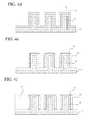
- FIGS. 1 a and 1 bare sectional views of a semiconductor device.
- FIGS. 2 a to 2 dare sectional views of a combination of forming storage device.
- FIGS. 3 a to 3 hare sectional views of steps in forming pillar shape storage devices.
- FIGS. 4 a to 4 jare sectional views of steps in forming cylinder shape storage devices.
- FIGS. 5 a to 5 kare sectional views of steps in forming a semiconductor memory device.
- FIGS. 6 a to 6 hare sectional views of steps in forming a semiconductor memory device.
- FIGS. 7 a to 7 hare sectional views of steps in forming a semiconductor memory device.
- FIGS. 8 a to 8 jare sectional views of steps in forming a semiconductor memory device.
- a method for fabricating semiconductor memory deviceis provided.
- the method for fabricating semiconductor memory deviceis comprising: providing a semiconductor substrate; forming lower region first data storage devices on the semiconductor substrate; forming switching devices on the first data storage devices; forming upper region second data storage devices on the switching devices; wherein forming the first and second data storage devices comprises; forming first electrodes in cylinder or pillar shape to be connected to the switching devices.
- FIGS. 1 a and 1 bare sectional views of a semiconductor device.
- the semiconductor memory deviceincludes first storage devices 1 , 4 which are formed on the semiconductor substrate; first switching devices 2 , 5 which are formed on the first storage devices 1 , 4 ; and second storage devices 3 , 6 which are formed on the first switching devices 2 , 5 .
- the semiconductor memory devicefurther includes, third storage devices (not illustrated) below the first storage devices 1 , 4 or above the second storage devices 3 , 6 ; second switching devices (not illustrated); and fourth storage devices (not illustrated).
- Each of the first, second, third and fourth storage devicescan be formed to include a first conductor, dielectric layer and a second conductor.
- the first switching devices 2 , 5can be formed vertically as shown in FIG. 1 a or horizontally as shown in FIG. 1 b.
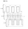
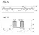
- FIGS. 2 a to 2 dillustrate combinations of shapes of forms of the storage devices in accordance with an embodiment of this invention.
- the first, second, third and fourth storage devicescan be formed in pillar or cylinder shapes.
- FIG. 2 aillustrates a structure formed with combination of the pillar shape first storage devices 10 a and the pillar shape second storage devices 20 a .
- FIG. 2 billustrates a structure formed with combination of the first pillar shape storage devices 10 b and the second cylinder shape storage devices 20 b .
- FIG. 2 cillustrates a structure formed with the cylinder shape first storage devices 10 c and the pillar shape storage devices 20 c .
- FIG. 2 dillustrates a structure formed with combination of the first cylinder shape storage devices 10 d and the second cylinder shape storage devices 20 d .
- the first switching devices 20 a , 20 b , 20 c , 20 dare included to all of four structures.
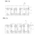
- FIGS. 3 a to 3 gare sectional views of steps in forming pillar shape storage devices in accordance with an embodiment of this invention.
- pillar shape patternsare formed on the semiconductor substrate 41 in order to forming lower region data storage devices by depositing insulator film or poly silicon film and then performing photolithography/etching processes.
- a first conductor 42is formed by depositing refractory metal or poly silicon film on the pillar shape patterns, and then a dielectric film 43 is formed on the first conductor 42 .
- refractory metal or poly silicon filmis deposited on the dielectric film 43 , and then refractory metal or the poly silicon film is planarized to form a second conductor (capacitor storage node) 44 .
- the second conductor (capacitor storage node) 44is photolithography/etched to separate the second conductor 44 .
- Top of the second conductor 44is processed to have enough area to allow enough alignment margin to following process steps which are contact photolithography and etching processes.
- Next stepis depositing insulation film 45 on the second conductor 45 with a pre-defined thickness.
- contact holesare formed in the insulation film 45 to expose the second conductor 44 , and then bit line for upper region storage devices 46 , bonding layer 51 , switching devices 52 , bit line for lower region storage devices 53 is formed.
- the upper region storage devices 60are formed on the formed structure as shown in FIG. 3 f .
- the method of forming the upper region storage deviceswill be described in description of an embodiment of this invention.
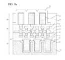
- FIGS. 4 a to 4 iare sectional views of steps in forming cylinder shape lower region storage devices in accordance with an embodiment of this invention.
- cylinder shape patternsare formed on the semiconductor substrate 71 in order to forming lower region data storage devices by depositing insulator film or poly silicon film and then performing photolithography/etching processes.
- a first conductor 72is formed by depositing refractory metal or poly silicon film on the pillar shape patterns, and then a dielectric film 73 is formed on the first conductor 72 .
- refractory metal or poly silicon filmis deposited on the dielectric film 73 to form a second conductor (capacitor storage node) 74 .
- the second conductor (capacitor storage node) 74is photolithography/etched to separate the second conductor 44 .
- a spacer etching processis performed to separate bottom of the second conductors 74 .
- the dielectric film used for the storage devicescan be formed with Atomic Layer Deposition (ALD) films such as Al2O3, HfO2 and ZrO2 which have good etch selectivity to the conductor material (refractory metal or poly silicon).
- ALDAtomic Layer Deposition
- a pre-defined thickness of insulation film 75is deposited on the second conductor 74 and then planarized by combination of CMP and etch back processes.
- part of the spacerswhich are conductor material and formed as spacer as shown in FIG. 4 d , can be exposed so that they can be connected at third conductor deposition process.
- a third conductors 76are formed.
- the third conductors 76are separated by photolithography and etching processes. Top of the third conductor 76 is processed to have enough area to allow enough alignment margin to following process steps which are contact photolithography and etching processes.
- contact holesare formed in the insulation film to expose the third conductor 76 , and then bit line for upper region storage devices 77 , bonding layer 81 , switching devices 82 , bit line for lower region storage devices 83 is formed.
- the upper region storage devices 90are formed on the formed structure as shown in FIG. 4 f .
- the method of forming the upper region storage deviceswill be described in description of an embodiment of this invention.
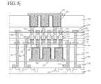
- FIGS. 5 a to 5 kare sectional views of steps in forming a semiconductor memory device in accordance with a first embodiment of this invention.
- logic devicesare formed on a first semiconductor substrate 100 .
- the logic devicescan be comprised of NMOS and PMOS transistors 110 , 112 , resisters(not illustrated), diodes(not illustrated) and wirings (not illustrated) on the first semiconductor substrate 100 .
- isolation films 102are formed in the first semiconductor substrate 100 to define active regions.
- the first semiconductor substrate 100can be bulk silicon, bulk silicon-germanium, or silicon or silicon-germanium epitaxial layer grown on the bulk silicon or bulk silicon-germanium substrate.
- the first semiconductor substrate 100can include silicon-on-sapphire (SOS), silicon-on-insulator (SOI), thin film transistor (TFT), doped or undoped semiconductors, silicon epitaxial layer on the base semiconductor substrate, or any other semiconductor materials that are well known to those skilled in the art.
- the isolation films 201can be formed by forming trenches in the first semiconductor substrate 100 and then fill in the trenches with insulation films such as High Density Plasma(HDP) oxide.
- insulation filmssuch as High Density Plasma(HDP) oxide.
- Well regionsin which the NMOS and PMOS transistors are formed, can be formed in a pre-defined region in the first semiconductor substrate 100 .
- the well regionscan be formed by ion-implanting dopants into the surface of the first semiconductor substrate 100 .
- gate dielectric and gate conductorare deposited and patterned to form gate conductors 110 .
- dopantsare ion-implanted to each side of the gate conductors 110 into the first semiconductor substrate 100 to form source/drain regions 112 . This completes transistors on the first semiconductor substrate 100 .
- a first interlayer insulation film 120is formed by depositing insulation film with good step coverage on the transistors. Resistors (not illustrated), diodes (not illustrated), and wirings (not illustrated) can be included in the first interlayer insulation film 120 .
- lower region storage devicesare formed on the first interlayer insulation film 120 in which the logic devices are included.
- the lower region data storage devicescan be formed as capacitors.
- the lower region data storage devicescan be formed as storage devices using phase-shift storage devices.
- the lower region data storage devicescan be also formed as ferroelectric memory device which is using ferroelectric characteristics of the material.
- the capacitorscan be formed in variety of shapes such as stack type, pillar type and cylinder type.
- first and second conductorscan be stacked face to face.
- first conductorcan be formed in pillar shape and then second conductor can be formed on the outer surface of the first conductor conformal.
- first conductorcan be formed in cylinder shape, and then second conductor can be formed conformal to the inner wall of the first conductors.
- the first conductors 132which are plate conductors, are formed on the first interlayer insulation film 120 in which logic devices are buried in. More specifically, enough thickness of conductor film is deposited on the first interlayer insulation film 120 , and then the conductor film is photolithography/etched to form the first conductors 132 in pillar shape which have connected bottom to each other.
- a dielectric film (not illustrated) and conductor film for the second conductorare deposited conformal.
- the conductor film for the second conductor 132are etched to separate the conductor film for the second conductor from the second conductors 134 .
- the second conductors 134can be formed to be separated each other as well as cover the surface of the pillar shape first conductors 132 .
- the second conductors 134also can be formed in cylinder shape which has open bottom as storage node conductor.
- the first and second conductorscan be formed with poly silicon or metal, and the dielectric film (not illustrated) can be formed with single layer of tantalum oxide (Ta2O5) or aluminum oxide (Al2O3) or stacked film of tantalum oxide/titanium oxide or aluminum oxide/titanium oxide.
- an insulation filmsuch as oxide film is deposited all over the surface.
- a second interlayer insulation film 140 , 150are formed by planarization process such as chemical-mechanical polishing (CMP) or etch-back processes.
- contact plugs 162 for lower region storage nodewhich are individually connected to the second conductors 134 and contact plugs 164 for the first logic which are connected to the transistors (logic devices in the lower region) are formed.
- Conductor lines 174are formed on the contact plugs 162 , 164 .
- conductor linescan be also formed on the capacitors 132 , 134 as not connected to the contact plugs for the lower region storage node.
- the conductor lines which are not connected to the contact plugs 162 for the lower region storage nodesare bit lines 172 which will be connected to the switching devices which will be formed at following process steps. Specifically, the bit lines 172 and conductor lines 174 can be formed alternatively in order on the capacitors 132 , 134 .
- a third interlayer insulation filmis formed 180 which covers the bit lines 172 and conductor lines 174 , and contact plugs 182 are formed which are electrically connected to the bit lines 172 and the second conductors 134 in the third interlayer insulation film 180 .
- a bonding layer 190is formed to bond a second semiconductor substrate 200 in which switching devices will be formed.
- the bonding layer 190can be formed with, for example, photo-setting adhesive such as reaction-setting adhesive, thermal-setting adhesive, photo-setting adhesive such as UV-setting adhesive, or anaerobe adhesive. Further, the bonding layer can be, such as, metallic bonds(Ti, TiN, Al), epoxy, acrylate, or silicon adhesives.
- the metalcan have lower melting temperature than the conductor materials used for the lower region contact plugs 162 , 164 and conductor lines 172 , 174 .
- the bonding layer 190can be formed with materials with reflow characteristics at low temperature so that creation of void can be reduced during a bonding process between the bonding layer 190 and the second semiconductor substrate 200 .
- the bonding layer 190can increase bonding strength as well as reduce micro defects such as micro voids.
- the second semiconductor substrate 200is bonded on the bonding layer 190 .
- the second semiconductor substratecan be a single crystalline semiconductor substrate which has multiple doping layers 201 , 203 , 205 in pre-defined depths from the surface.
- the multiple doping layers 210 , 203 , 205can be formed by ion-implanting dopants into the surface of the single crystalline semiconductor substrate or by adding dopants during an epitaxial growth process to form the single crystalline semiconductor substrate.
- the multiple doped layer 200can be formed by ion-implanting dopants to arrange n-type doped layer 201 , 205 and p-type doped layer 203 located alternatively.
- n-type doped layer 201is formed on the surface of the multiple doped layers 201 , 203 , 205 so that the n-type doped layer is bonded to the bonding layer 190 and eventually forms NMOS transistors.
- a detaching layer 207is included in between the interface of the multiple doped layers 201 , 203 , 205 and the single crystalline semiconductor substrate.
- the detaching layercan be formed as porous layer, insulation film layer such as oxide or nitride, organic bonding layer, or strained layer which is formed by crystalline lattice difference such as Si—Ge.
- one technologyis called as exfoliating implant in which gas phase ions such as hydrogen is implanted to form the detaching layer, but in this technology, the crystal lattice structure of the multiple doped layers 201 , 203 , 205 can be damaged.
- a thermal treatment under very high temperature and long timeshould be performed, and this can strongly damage the cell devices underneath.
- the detaching layer 207can protect the multiple doped layers 201 , 203 , 205 when the second semiconductor substrate 200 is bonded onto the bonding layer 190 and then the single crystalline semiconductor substrate is removed. Also, the detaching layer 207 helps to clearly separate the single crystalline semiconductor substrate while precisely and easily remaining only the multiple doped layers 201 , 203 , 205 .
- the second semiconductor substrate 200is bonded to the bonding layer 190 to be face to face to the multiple doped layers 201 , 203 , 205 .
- a heat treatment under a pressurecan be performed after bonding the second semiconductor substrate to surface of the bonding layer 190 .
- grinding or polishing processcan be performed at the single crystalline semiconductor region until the detaching layer 207 is exposed from the bonded second semiconductor substrate 200 .
- anisotropic or isotropic etch processcan be performed to expose surface of the multiple doped layers 201 , 203 , 205 . That is, the n-type doped layer 205 is exposed.
- a physical shockcan be applied to the detaching layer 207 so that a crack is created at and along the detaching layer and eventually the crack separates the single crystalline semiconductor substrate and the multiple doped layers 201 , 203 , 205 .
- n-type doped layer 201 , p-type doped layer 203 , and n-type doped layer 205can be created in order on the bonding layer 190 by bonding the second semiconductor substrate 200 which includes multiple doped layers 201 , 203 , 205 on the bonding layer 190 and then removing the single crystalline semiconductor substrate only except the multiple doped layers 201 , 203 , 205 .
- Pillar shape semiconductor patterns 202 , 204 , 206are formed to create switching devices, those are transistors, with vertical channel structure. Pillar shape semiconductor patterns 202 , 204 , 206 are formed by patterning the multiple doped layers 201 , 203 , 205 so that they can become channeled region 204 and source/drain region 202 , 206 of the switching device.
- the semiconductor patterns 202 , 204 , 206can be formed by performing photolithography/etch process to the multiple doped layers. More specifically, n/p/n type doped layers pattern can be formed.
- the bonding layer 190also can be etched when forming the semiconductor patterns 202 , 204 , 206 . In this case, bonding layer pattern 190 can be formed underneath of each of the pillar shape semiconductor patterns 202 , and part of surface of the third interlayer insulation film 180 can be exposed.
- a gate conductor 220is formed as spacer shape around the center area ( 204 ) of the semiconductor patterns 202 , 204 , 206 .
- a fourth interlayer insulation film 210is formed on the third interlayer insulation film 180 which covers the sidewall of the semiconductor pattern 202 which is bonded to the bonding layer 190 .
- Gate contact plugsare formed in the third and fourth interlayer insulation film 180 , 210 in order to connect logic devices in the lower region and gate conductor 220 .
- gate dielectric film and gate conductor filmare deposited on the fourth interlayer insulation film 210 , conformal to the surface of the semiconductor patterns.
- the gate dielectric film and the gate conductor filmcan be anisotropic etched to form a spacer shape gate conductor 220 which surrounds the p-type semiconductor pattern 204 which is located in center and roles as channel region. As a result, transistors which have vertical channel can be formed.
- a fifth interlayer insulation film 230is formed to cover the pillar shape semiconductor patterns 202 , 204 , 206 and the gate conductors 220 . Then, source/drain contacts plugs 242 are formed to respectively contact to source/drain regions 206 in the fifth interlayer insulation film 230 , and at the same time second contact plugs for logic 244 can be formed which contact to logic devices. Conducting lines 252 , 254 are formed on the each contact plugs 242 , 244 . The conducting lines 252 , which are located on the semiconductor patterns 202 , 204 , 206 which are connected to the capacitors 132 , 134 , can be bit lines.
- a sixth interlayer insulation film 260is formed, and then contact plugs 262 for upper region storage node which are connected to the conducting lines 252 can be selectively formed.
- Contact plugs 262 for upper region storage node which will connect the second conductor and the source/drain region 206is formed on the semiconductor patterns 202 , 204 , 206 to which capacitors 132 , 134 are not connected below among the semiconductor patterns 202 , 204 , 206 .
- upper region capacitorsare formed as upper region data storage devices.
- the upper region data storage devicesare formed to be symmetric to the lower region data storage devices, and can be connected to the switching devices which are not connected to the lower region data storage devices.
- the switching devices connected to the lower region data storage devicescan be arranged alternative in order to the switching devices connected to the upper region data storage devices.
- the upper data storage devicescan be formed in cylinder shape.
- a seventh interlayer insulation film 270is formed to have enough thickness on the sixth interlayer insulation film 260 .
- the seventh interlayer insulation film 270is then patterned to have openings which expose top side of the contact plugs 262 for the upper region storage nodes.
- a conducting film for second conductor of upper capacitoris deposited conformal to the surface of the seventh interlayer insulation film 270 in where the openings are formed. Then a insulation film with good gap filling characteristics (not illustrated) is deposited and then the conducting film for the second conductor is planarized until the seventh interlayer insulation film 270 is exposed, to form the cylinder shape second conductors 282 .
- a dielectric film(not illustrated) is deposited conformal to the surface of the second conductors 282 and then conducting film for the first conductor is deposited to fill up inside of the second conductors 282 .
- the conducting film for the first conductoris then patterned to form the first conductors 284 .
- an eighth interlayer insulation film 280can be formed on the seventh interlayer insulation film 270 to cover the upper region data storage devices 282 , 284 .
- third contact plugs for logic 292 and wirings 294can be formed which are connected to the logic devices.
- switching devicescan be formed on the logic devices by bonding a semiconductor substrate and those switching devices can have vertical channel.
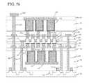
- FIGS. 6 a to 6 hA method for fabricating a semiconductor device in accordance with a second embodiment of this invention if illustrated in FIGS. 6 a to 6 h.
- logic devicesare formed on the first semiconductor substrate 300 .
- NMOS and PMOS transistors 310 , 312 , resistors (not illustrated), diodes (not illustrated) and wirings (not illustrated)are formed on the first semiconductor substrate 300 to form the logic devices.
- isolation films 302are formed in the first semiconductor substrate 300 to define active region.
- Gate dielectric film and gate conductor filmcan be deposited and patterned to form gate electrodes 310 , on the first semiconductor substrate 300 in which the active regions are formed.
- dopantsare ion-implanted to the each side of the gate conductor 310 to form source/drain regions 312 .
- transistorsare formed on the first semiconductor substrate 300 .
- a first interlayer insulation film 320is formed by depositing insulation film with good step coverage on the transistors 310 , 312 . Resistors (not illustrated), diodes (not illustrated) and wirings (not illustrated) can be included in the first interlayer insulation film 320 .
- lower region data storage devicesare formed on the first interlayer insulation film 320 in which the logic devices are buried.
- capacitorscan be used for lower region data storage devices.
- First electrodes 332are formed as plate electrodes, on the first interlayer insulation film 320 in which logic devices are buried. Specifically, a conducting film for the first electrodes is deposited with enough thickness on the first interlayer insulation film 320 , and the conducting film for the first electrodes are photolithography/etched to form pillar shape first electrodes 332 . The first electrodes can be electrically connected each other to where ground potential is applied.
- a dielectric film (not illustrated) and a conducting film for second electrodesare deposited conformal.
- the conducting film for the second electrodesis etched to isolate and separate the conducting film for the second electrodes into the second electrodes 334 .
- the second electrodes 334are covering the pillar shape first electrodes 332 conformal and the second electrodes 334 are separated each other.
- the second electrodes 334are storage node electrodes and can be formed in cylinder shape which has a open bottom.
- second interlayer insulation film 340 , 350is deposited.
- the second interlayer insulation filmscan be oxide.
- the top surface of the second interlayer insulation film 340 , 350can be planarized by CMP or etchback processes.
- contact plugs 362 and conducting pads 372can be formed to be connected to the second electrodes 334 .
- the lower region data storage devices on the first interlayer insulation film 320can be formed by refractory metal materials which has characteristics such as low resistance, low stress, good step coverage and good thermal expansion coefficient in order to reduce affection from the following high temperature processes.
- the first and second electrodes 332 , 334 of the capacitors, contact plugs 362 , and conducting pads 372can be formed with refractory metal.
- the refractory metalcan be of many different types, such as tungsten (W), titanium (Ti), molybdenum (Mo), tantalum (Ta), titanium nitride (TiN), tantalum nitride (TaN), zirconium nitride (ZrN), tungsten nitride, and alloys thereof.
- first and second electrodes 332 , 334can be formed with poly-silicon film.
- the electric characteristics and reliabilities of the lower region data storage devicescan be maintained even after the following high temperature process steps(i.e. switching device formation process steps).
- a third interlayer insulation film 380are formed and planarized to cover the conducting pads 372 on the lower region capacitors 332 , 334 . Then, a bonding layer 390 is formed on the third interlayer insulation film 380 .
- the bonding layer 390is for bonding a second semiconductor substrate 400 , and formed on the most upper layer of the first semiconductor substrate 300 .
- the bonding layer 390can be photo-setting adhesive such as reaction-setting adhesive, thermal-setting adhesive, photo-setting adhesive such as UV-setting adhesive, or anaerobe adhesive.
- the metalcan have lower melting temperature than the conductor materials used for the lower region contact plugs 362 and conductor lines 372 .
- the bonding layer 390can be formed with materials with reflow characteristics at low temperature so that creation of void can be reduced during a bonding process between the bonding layer 390 and the second semiconductor substrate 400 .
- the bonding layer 390can increase bonding strength as well as reduce micro defects such as micro voids.
- the second semiconductor substrate 400is bonded onto the bonding layer 390 .
- the second semiconductor substrate 400is a single crystalline semiconductor substrate and is prepared to have doped layers 401 which has doped layers in a pre-defined depths.
- the doped layers 401can be formed by ion-implanting dopants into the single crystalline semiconductor substrate or by adding dopants during epitaxial process to grow single crystalline semiconductor substrate.
- a detaching layer 407can be formed in a pre-defined depth in the single crystalline semiconductor substrate and the detaching layer 407 is interfacing with the doped layer 401 .
- the detaching layer 407can be a porous layer including many micro voids, an insulation film such as oxide or nitride, an organic bonding layer, or a strained layer by crystal lattice structure difference (for example Si—Ge). Also, the bonding layer can be also formed on the surface of the doped layer 401 .
- the second semiconductor substrate 400is then bonded onto the bonding layer 390 , to face the doped layer 401 of the second semiconductor substrate to face the bonding layer of the first semiconductor substrate 300 .
- a thermal treatmentcan be performed under certain pressure in order to increase bonding strength.
- grinding or polishing processcan be performed at the single crystalline semiconductor region until the detaching layer 407 is exposed from the bonded second semiconductor substrate 400 .
- anisotropic or isotropic etch processcan be performed to expose surface of the doped layers.
- transistorswhich are switching devices having horizontal channels on the bonded single crystalline semiconductor doped layers 401 , can be formed.
- isolation films 402are formed to define active regions in the bonded single crystalline semiconductor doped layers 401 .
- Gate dielectric film and gate conductor filmare deposited and patterned to form gate electrodes 410 on the single crystalline semiconductor doped layers 401 .
- Dopantsare doped in the single crystalline semiconductor doped layers 401 at each side of the gate electrodes 410 to form source/drain regions 412 , 414 .
- Neighboring gate electrodes 410can share common source region 412 .
- the drain regions 414can be formed at apart from the sources regions 412 and close to gate electrode 410 sidewalls in the single crystalline semiconductor doped layers 401 .
- Particular drain regions 414can be formed on the lower regions capacitors 332 , 334 , when forming the transistors.
- the source/drain regions 412 , 414 at each side of the gate electrodes 410can be formed by dopant ion-implantation and annealing processes.
- the ion-implantation and annealing processcan be performed at high temperatures of 800-850 degree Celsius. Even though in the high temperature environment, the lower region data storage devices formed under the switching devices are formed with refractory metals so that reliability decrement by the high temperature process can be prevented.
- a fourth interlayer insulation film 420is formed to cover the transistors 410 on the second semiconductor substrate 400 .
- Contact holes 421are formed by penetrating the fourth interlayer insulation film 420 and the doped layer 401 to expose the conducting lines 472 on the lower regions capacitors 432 , 434 .
- an insulation filmis deposited along to the surface of the contact holes 421 and etched anisotropic to form spacer shape insulation spacers 422 .
- the insulation spacers 422can prevent exposing of the bonding layer 390 , which is a conducting film, by the contact holes 421 .
- contact plugs 424 for the lower region storage nodesare formed by partially burying conducting material into the contact holes 421 which are penetrating the doped layers 401 .
- the contact plugs 424 for the lower region storage nodescan be buried up to the surface of the doped layers 401 , and electrically connected to the drain region 414 formed in the second semiconductor substrate 400 .
- a fifth interlayer insulation film 430is formed to cover contact holes on the fourth interlayer insulation film 420 .
- Contact plugs 432 for but linesare formed which contact to the common source region 412 in the fourth and fifth interlayer insulation film 420 , 430 .
- Contact plugs for electrically connected to the logic devicescan be formed when the contact plugs for bit lines 432 are formed.
- bit lines 434are formed on the contact plugs 432 for the bit lines so that the bit lines are running cross to the gate electrodes 410 .
- Conducting lines (not illustrated) which are connected to the logic devicescan be formed when the bit lines 434 are formed.
- a sixth interlayer insulation film 440is formed to cover the bite lines 434 , and contact plugs 442 for the upper region storage nodes are formed in the sixth interlayer insulation film 440 which are connected to the drain region 414 .
- bit lines 434 and the contact plugs 442 for the storage nodeare electrically insulated.
- second electrodes 452can be formed as open top cylinder shape on the contact plugs 442 for the upper region storage node. Then, a dielectric film (not illustrated) and first electrodes 454 can be formed on the second electrodes 452 . The first electrodes 454 can fill in the cylinder shape second electrodes 452 .
- a eighth interlayer insulation film 470is formed to cover the upper regions capacitors 452 , 454 , and contact plugs 482 and final metal wirings 492 for connecting to the logic devices 310 , 312 are formed.
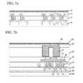
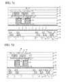
- FIGS. 7 a to 7 hare sectional views of steps in forming a semiconductor memory device in accordance with a third embodiment of this invention.
- a first semiconductor substrateis provided.
- Logic devicesare already formed on the first semiconductor substrate.
- transistors 510 , 512are formed on the first semiconductor substrate 500 , and a first interlayer insulation film 520 is formed to cover the transistors 510 , 512 .
- Contact plugsare formed in the first interlayer insulation film 520 , and wiring 522 can be formed on the contact plugs.
- a second interlayer insulation film 530is formed to cover the wirings 522 and then surface is planarized.
- a bonding layer 540is formed on the second interlayer insulation film 530 .
- a second semiconductor substrate 600is provided.
- the second semiconductor substrate 600includes switching devices 610 , 612 , 614 and first data storage devices 642 , 644 .
- the second semiconductor substrate 600can be a single crystalline semiconductor substrate including doped layer 600 b which has dopants doped to a pre-defined depth from surface of the second semiconductor substrate 600 .
- the single crystalline semiconductor substrateincludes doped layer 600 b to a pre-defined depth from the top surface.
- a detaching layer 605can be included in the single crystalline semiconductor substrate and the detaching layer 605 is interfacing with the doped layer 600 b.
- Transistors with horizontal channel 610 , 612 , 614are formed on the second semiconductor substrate 600 .
- a first interlayer insulation film 620is deposited to cover the transistors 610 , 612 , 614 , and contact plugs 622 for bit line and bit lines 624 are formed step by step.
- the contact plugs 622are connected to the common source region of the transistors.
- a second interlayer insulation film 630is formed to cover the bit lines, and contact plugs for storage nodes 632 are formed in the first and second interlayer insulation film 620 , 630 .
- capacitors 642 , 644are formed on the each of the contact plugs for the storage node 632 .
- a dielectric film (not illustrated) and plate electrode 644are formed to cover the storage node electrodes 642 .
- a fourth interlayer insulation film 650is formed to cover the capacitors 642 , 644 , and a bonding layer 655 is formed on the fourth interlayer insulation film 650 .
- the first semiconductor substratewhich includes the logic devices 510 , 512 , 522 and the second semiconductor substrate 600 which includes switching devices 610 , 612 , 614 and the data storage devices 642 , 644 are bonded together.
- the bonding layer 540 on the first semiconductor substrate 500 and the bonding layer 655 on the second semiconductor substrate 600are facing each other to be bonded to form the second semiconductor substrate 600 on the first semiconductor substrate 500 .
- the first data storage devices 642 , 644 and the switching devices 610 , 612 , 614are formed following the order.
- part of backside 600 a of the second semiconductor substrate 600is removed.
- the detaching layer 605 in the second semiconductor substrate 600can control the removing of part of the second semiconductor substrate 600 .
- contact plugs 608are formed to be connected to the selected drain region 614 of the transistors in the second semiconductor substrate 600 .
- second data storage devices 662 , 664are formed on the backside surface of the second semiconductor substrate 600 .
- capacitors 662 , 664are formed to be connected to the contact plugs 608 at the backside surface of the second semiconductor substrate 600 .
- open top cylinder shape storage node electrodes 662are formed, and then a dielectric film (not illustrated) and plate electrode 664 are formed.
- contact plugs 672 , 684 , 676 and conducting lines 685are formed corresponding to each of the bit lines 624 , gate electrodes 610 and logic devices 510 , 512 .
- an insulation film 680is formed to cover the conducting lines 678 , and a bonding layer 685 is formed on the interlayer insulation film 680 .
- a third semiconductor substrate 700which includes switching devices 710 , 712 , 714 and third data storage devices 742 , 744 is provided, a bonding layer 755 is formed on the top surface of the third semiconductor substrate 700 , and the bonding layer 755 is bonded to the bonding layer 685 of the second semiconductor substrate 600 .
- formation of the switching devices 710 , 712 and the third data storage devices 742 , 744 on the third semiconductor substrate 700can be similar to the formation of the switching devices 510 , 512 and the second data storage devices 610 , 612 , 614 on the second semiconductor substrate 600 as illustrated in FIG. 7 b.
- part of the backside of the third semiconductor substrate 700is removed, and then fourth data storage devices 762 , 764 are formed to be electrically connected to the switching devices 710 , 712 .
- contact plugs for storage nodeare formed to be connected to the drain region 714 of the transistors in the third semiconductor substrate 700 .
- Capacitors 762 , 764are formed on the contact plugs for storage node. More specifically, the third data storage devices 742 , 744 are formed below the switching devices 710 , 712 , and the fourth data storage devices 762 , 764 can be formed above the switching devices 710 , 712 .
- contact plugs 772 , 774 and conducting lines 778are formed to be connected respectively to each of the bit lines 724 and gate electrodes 310 on the third semiconductor substrate 700 .
- contact plugs 778 and conducting lines 778are formed to be connected to the lower region logic devices 510 , 512 , 522 .
- final metal wirings 784are formed on the contact plugs 778 which is connected to the logic devices 510 , 512 , 522 .
- the switching devices and the data storage devicescan be formed on top of the logic devices. It should be noted that by repeating the bonding of the semiconductor substrates with switching devices and the semiconductor substrate with the data storage devices on the logic devices, the chip density of the semiconductor memory device can be increased.
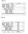
- a first semiconductor substrate 800is provided.
- the first semiconductor substrate 800includes a bonding layer 810 on the surface.
- the first semiconductor substrate 800can be also a substrate not having any doped layers or other devices.
- a second semiconductor substrate 900is provided.
- the second semiconductor substrate 900includes switching devices 910 , 912 , 914 and first data storage devices 942 , 944 .
- the second semiconductor substrate 900also includes a detaching layer 905 which can act as an etch stopper when removing part of the second semiconductor substrate in following process steps.
- the forming method of the switching devices 910 , 912 , 914 and the first data storage devices 942 , 944can be similar to the method as described with FIG. 5 b .
- an interlayer insulation film 950is formed to cover the first data storage devices 942 , 944 , and a bonding layer 955 is formed on the interlayer insulation film 950 .
- the bonding layer 810 of the first semiconductor substrate 800 and the bonding layer 955 of the second semiconductor substrate 900are bonded together face to face.
- the second semiconductor substrate 900is on top of the first semiconductor substrate 800 , and backside of the second semiconductor substrate 900 is exposed.
- data storage device 942 , 944 and switching devices 910 , 912can be arranged in order on the first semiconductor substrate 800 . Then, part of the backside of the second semiconductor substrate 900 is removed. The detaching layer 905 formed in the second semiconductor substrate 900 can be also removed when part of the backside of the second semiconductor substrate 900 is removed.
- second data storage devices 962 , 964are formed on the backside of the second semiconductor substrate 900 .
- contact plugs for storage node 908are formed to be connected to the drain region 914 in the second semiconductor substrate 900 .
- Capacitors 942 , 944are formed on the contact plugs for the storage node.
- Contact plugs 908 and wirings 978are formed to be respectively connected to the bit lines 924 and gate electrodes 910 .
- contact plugs 820are formed to be connected from the third semiconductor substrate 800 to the wirings 978 , for connection to the logic devices which will be bonded at following process steps.
- a bonding layer 830is formed at the backside of the third semiconductor substrate 800 . This completes preparation of the first semiconductor device A.
- a second semiconductor device Bis provided.
- the second semiconductor device Bcomprises of a third semiconductor substrate 1100 and bonding layers 1130 , 1290 at each of the backside and frontside.
- the forming method of the second semiconductor device Bis similar to that of the first semiconductor device A as described with FIGS. 8 a to 8 d .
- bonding layers 1130 , 1290can be formed at top front side of the first data storage devices 1242 , 1244 (i.e. backside of the dummy semiconductor substrate 1100 ) and at top front side of the first data storage devices 1262 , 1264 .
- a fourth semiconductor substrate 1300is provided.
- the fourth semiconductor substrate 1300includes logic devices 1310 , 1312 , 1322 .
- the fourth semiconductor substrate 1300can include transistors 1310 , 1312 and wirings 1322 that are connected to the transistors.
- contact plugs 1340are formed to be connected to the wirings 1322 on the fourth semiconductor substrate 1300 from backside of the fourth semiconductor substrate 1300 .
- the contact plugs 1340can be formed by penetrating the fourth semiconductor substrate 1300 .
- Wirings 1350can be formed to be electrically connected to the logic devices 1310 , 1312 at the backside of the fourth semiconductor substrate 1300 .
- a bonding layer 1360is formed on top of the fourth semiconductor substrate 1300 for bonding other semiconductor devices A, B.
- the bonding layer 1360can be formed with conducting material, and the logic devices 1310 , 1312 can be electrically connected to the other semiconductor devices A, B through the bonding layer 1360 .
- the second semiconductor device Bis bonded on the third semiconductor device C. Then, the first semiconductor device A is bonded on the second semiconductor device B.
- the semiconductor memory deviceincludes data storage devices and switching devices arranged alternatively on top of the logic devices 1310 , 1312 .
- the first, the second and the third semiconductor devicescan be electrically connected through the bonding layers 1130 , 1290 because the bonding layers 1130 , 1290 can be formed with conducting material.
Landscapes
- Engineering & Computer Science (AREA)
- Manufacturing & Machinery (AREA)
- Semiconductor Memories (AREA)
Abstract
Description
Claims (20)
Applications Claiming Priority (3)
| Application Number | Priority Date | Filing Date | Title |
|---|---|---|---|
| KR1020100063938AKR101134819B1 (en) | 2010-07-02 | 2010-07-02 | Method for fabricating semiconductor memory |
| KR10-2009-63938 | 2010-07-02 | ||
| KR10-2009-0063938 | 2010-07-02 |
Publications (2)
| Publication Number | Publication Date |
|---|---|
| US20120003808A1 US20120003808A1 (en) | 2012-01-05 |
| US9012292B2true US9012292B2 (en) | 2015-04-21 |
Family
ID=45400023
Family Applications (1)
| Application Number | Title | Priority Date | Filing Date |
|---|---|---|---|
| US13/175,652Expired - Fee RelatedUS9012292B2 (en) | 2010-07-02 | 2011-07-01 | Semiconductor memory device and method of fabricating the same |
Country Status (2)
| Country | Link |
|---|---|
| US (1) | US9012292B2 (en) |
| KR (1) | KR101134819B1 (en) |
Cited By (7)
| Publication number | Priority date | Publication date | Assignee | Title |
|---|---|---|---|---|
| US10283411B1 (en)* | 2018-01-02 | 2019-05-07 | International Business Machines Corporation | Stacked vertical transistor device for three-dimensional monolithic integration |
| US10734371B2 (en) | 2018-11-06 | 2020-08-04 | Samsung Electronics Co., Ltd. | Semiconductor device |
| US20220406834A1 (en)* | 2019-11-19 | 2022-12-22 | Sony Semiconductor Solutions Corporation | Semiconductor device, solid-state imaging device and electronic device |
| WO2023278933A1 (en) | 2021-06-30 | 2023-01-05 | Micron Technology, Inc. | Methods of forming microelectronic devices, and related microelectronic devices and electronic systems |
| US20230088864A1 (en)* | 2021-09-17 | 2023-03-23 | Kioxia Corporation | Semiconductor memory device |
| EP4203003A1 (en)* | 2021-12-21 | 2023-06-28 | INTEL Corporation | Ic structure with multiple levels of embedded memory |
| US12262532B2 (en) | 2021-06-30 | 2025-03-25 | Micron Technology, Inc. | Microelectronic devices and electronic systems |
Families Citing this family (23)
| Publication number | Priority date | Publication date | Assignee | Title |
|---|---|---|---|---|
| KR20140046698A (en) | 2012-10-10 | 2014-04-21 | 에스케이하이닉스 주식회사 | Semiconductor device and method for manufacturing the same |
| US12051674B2 (en)* | 2012-12-22 | 2024-07-30 | Monolithic 3D Inc. | 3D semiconductor device and structure with metal layers |
| US9443869B2 (en)* | 2013-11-05 | 2016-09-13 | Taiwan Semiconductor Manufacturing Company Limited | Systems and methods for a semiconductor structure having multiple semiconductor-device layers |
| US20160043108A1 (en)* | 2014-08-07 | 2016-02-11 | Silanna Semiconductor U.S.A., Inc. | Semiconductor Structure with Multiple Active Layers in an SOI Wafer |
| CN105845544B (en)* | 2015-01-14 | 2021-02-19 | 中芯国际集成电路制造(上海)有限公司 | Method for manufacturing semiconductor device and electronic device |
| WO2019066967A1 (en)* | 2017-09-29 | 2019-04-04 | Intel Corporation | Ferroelectric capacitors with backend transistors |
| EP3688805A4 (en)* | 2017-09-29 | 2021-04-14 | INTEL Corporation | VERTICAL REAR SIDE TRANSISTOR WITH FERROELECTRIC MATERIAL |
| CN111755386A (en)* | 2019-03-29 | 2020-10-09 | 长鑫存储技术有限公司 | Method for manufacturing semiconductor structure |
| CN111755388B (en)* | 2019-03-29 | 2022-05-31 | 长鑫存储技术有限公司 | Method of making a semiconductor structure |
| CN111755387B (en)* | 2019-03-29 | 2022-06-03 | 长鑫存储技术有限公司 | Method of making a semiconductor structure |
| US11888034B2 (en) | 2019-06-07 | 2024-01-30 | Intel Corporation | Transistors with metal chalcogenide channel materials |
| US11171243B2 (en) | 2019-06-27 | 2021-11-09 | Intel Corporation | Transistor structures with a metal oxide contact buffer |
| US11777029B2 (en) | 2019-06-27 | 2023-10-03 | Intel Corporation | Vertical transistors for ultra-dense logic and memory applications |
| US11411011B2 (en) | 2020-06-18 | 2022-08-09 | Taiwan Semiconductor Manufacturing Company, Ltd. | Semiconductor structure having memory device and method of forming the same |
| US11424248B2 (en)* | 2020-09-25 | 2022-08-23 | Besang Inc. | Bitline structure for three-dimensional integrated circuit and method of forming the same |
| US12266720B2 (en) | 2020-12-21 | 2025-04-01 | Intel Corporation | Transistors with monocrystalline metal chalcogenide channel materials |
| US12120865B2 (en) | 2020-12-23 | 2024-10-15 | Intel Corporation | Arrays of double-sided dram cells including capacitors on the frontside and backside of a stacked transistor structure |
| US11862628B2 (en) | 2021-05-20 | 2024-01-02 | Micron Technology, Inc. | Transistor configurations for multi-deck memory devices |
| US12327809B2 (en)* | 2021-06-23 | 2025-06-10 | Intel Corporation | Vertically stacked and bonded memory arrays |
| US11837594B2 (en)* | 2021-06-30 | 2023-12-05 | Micron Technology, Inc. | Microelectronic devices and electronic systems |
| US20230200083A1 (en)* | 2021-12-21 | 2023-06-22 | Intel Corporation | Embedded memory with ferroelectric capacitors & independent top plate lines |
| US20230389324A1 (en)* | 2022-05-26 | 2023-11-30 | Taiwan Semiconductor Manufacturing Company, Ltd. | Ferroelectric-based memory device and method of forming the same |
| US20240196586A1 (en)* | 2022-12-09 | 2024-06-13 | International Business Machines Corporation | Stacked and non-stacked transistors with double-sided interconnects |
Citations (83)
| Publication number | Priority date | Publication date | Assignee | Title |
|---|---|---|---|---|
| US4704785A (en) | 1986-08-01 | 1987-11-10 | Texas Instruments Incorporated | Process for making a buried conductor by fusing two wafers |
| US4732312A (en) | 1986-11-10 | 1988-03-22 | Grumman Aerospace Corporation | Method for diffusion bonding of alloys having low solubility oxides |
| US4829018A (en) | 1986-06-27 | 1989-05-09 | Wahlstrom Sven E | Multilevel integrated circuits employing fused oxide layers |
| US4854986A (en) | 1987-05-13 | 1989-08-08 | Harris Corporation | Bonding technique to join two or more silicon wafers |
| US5087585A (en) | 1989-07-11 | 1992-02-11 | Nec Corporation | Method of stacking semiconductor substrates for fabrication of three-dimensional integrated circuit |
| US5106775A (en) | 1987-12-10 | 1992-04-21 | Hitachi, Ltd. | Process for manufacturing vertical dynamic random access memories |
| US5152857A (en) | 1990-03-29 | 1992-10-06 | Shin-Etsu Handotai Co., Ltd. | Method for preparing a substrate for semiconductor devices |
| US5250460A (en) | 1991-10-11 | 1993-10-05 | Canon Kabushiki Kaisha | Method of producing semiconductor substrate |
| US5266511A (en) | 1991-10-02 | 1993-11-30 | Fujitsu Limited | Process for manufacturing three dimensional IC's |
| US5277748A (en) | 1992-01-31 | 1994-01-11 | Canon Kabushiki Kaisha | Semiconductor device substrate and process for preparing the same |
| US5324980A (en) | 1989-09-22 | 1994-06-28 | Mitsubishi Denki Kabushiki Kaisha | Multi-layer type semiconductor device with semiconductor element layers stacked in opposite direction and manufacturing method thereof |
| US5355022A (en) | 1991-09-10 | 1994-10-11 | Mitsubishi Denki Kabushiki Kaisha | Stacked-type semiconductor device |
| US5371037A (en) | 1990-08-03 | 1994-12-06 | Canon Kabushiki Kaisha | Semiconductor member and process for preparing semiconductor member |
| US5374581A (en) | 1991-07-31 | 1994-12-20 | Canon Kabushiki Kaisha | Method for preparing semiconductor member |
| US5374564A (en) | 1991-09-18 | 1994-12-20 | Commissariat A L'energie Atomique | Process for the production of thin semiconductor material films |
| US5554870A (en) | 1994-02-04 | 1996-09-10 | Motorola, Inc. | Integrated circuit having both vertical and horizontal devices and process for making the same |
| US5563084A (en) | 1994-09-22 | 1996-10-08 | Fraunhofer-Gesellschaft zur F orderung der angewandten Forschung e.V. | Method of making a three-dimensional integrated circuit |
| US5617991A (en) | 1995-12-01 | 1997-04-08 | Advanced Micro Devices, Inc. | Method for electrically conductive metal-to-metal bonding |
| US5695557A (en) | 1993-12-28 | 1997-12-09 | Canon Kabushiki Kaisha | Process for producing a semiconductor substrate |
| US5854123A (en) | 1995-10-06 | 1998-12-29 | Canon Kabushiki Kaisha | Method for producing semiconductor substrate |
| US5882987A (en) | 1997-08-26 | 1999-03-16 | International Business Machines Corporation | Smart-cut process for the production of thin semiconductor material films |
| US5937312A (en) | 1995-03-23 | 1999-08-10 | Sibond L.L.C. | Single-etch stop process for the manufacture of silicon-on-insulator wafers |
| US5998808A (en) | 1997-06-27 | 1999-12-07 | Sony Corporation | Three-dimensional integrated circuit device and its manufacturing method |
| US6057212A (en) | 1998-05-04 | 2000-05-02 | International Business Machines Corporation | Method for making bonded metal back-plane substrates |
| US6103597A (en) | 1996-04-11 | 2000-08-15 | Commissariat A L'energie Atomique | Method of obtaining a thin film of semiconductor material |
| US6153495A (en) | 1998-03-09 | 2000-11-28 | Intersil Corporation | Advanced methods for making semiconductor devices by low temperature direct bonding |
| US6222251B1 (en) | 1997-01-27 | 2001-04-24 | Texas Instruments Incorporated | Variable threshold voltage gate electrode for higher performance mosfets |
| US6229161B1 (en) | 1998-06-05 | 2001-05-08 | Stanford University | Semiconductor capacitively-coupled NDR device and its applications in high-density high-speed memories and in power switches |
| US6242324B1 (en) | 1999-08-10 | 2001-06-05 | The United States Of America As Represented By The Secretary Of The Navy | Method for fabricating singe crystal materials over CMOS devices |
| US6331468B1 (en) | 1998-05-11 | 2001-12-18 | Lsi Logic Corporation | Formation of integrated circuit structure using one or more silicon layers for implantation and out-diffusion in formation of defect-free source/drain regions and also for subsequent formation of silicon nitride spacers |
| US20020025604A1 (en) | 2000-08-30 | 2002-02-28 | Sandip Tiwari | Low temperature semiconductor layering and three-dimensional electronic circuits using the layering |
| US6380099B2 (en) | 1998-01-14 | 2002-04-30 | Canon Kabushiki Kaisha | Porous region removing method and semiconductor substrate manufacturing method |
| US6380046B1 (en) | 1998-06-22 | 2002-04-30 | Semiconductor Energy Laboratory Co., Ltd. | Method of manufacturing a semiconductor device |
| US6417108B1 (en) | 1998-02-04 | 2002-07-09 | Canon Kabushiki Kaisha | Semiconductor substrate and method of manufacturing the same |
| US6423614B1 (en) | 1998-06-30 | 2002-07-23 | Intel Corporation | Method of delaminating a thin film using non-thermal techniques |
| US6534382B1 (en) | 1996-12-18 | 2003-03-18 | Canon Kabushiki Kaisha | Process for producing semiconductor article |
| US6555901B1 (en) | 1996-10-04 | 2003-04-29 | Denso Corporation | Semiconductor device including eutectic bonding portion and method for manufacturing the same |
| US20030102079A1 (en) | 2000-01-17 | 2003-06-05 | Edvard Kalvesten | Method of joining components |
| US20030119279A1 (en) | 2000-03-22 | 2003-06-26 | Ziptronix | Three dimensional device integration method and integrated device |
| US6630713B2 (en) | 1998-11-10 | 2003-10-07 | Micron Technology, Inc. | Low temperature silicon wafer bond process with bulk material bond strength |
| US6635552B1 (en) | 2000-06-12 | 2003-10-21 | Micron Technology, Inc. | Methods of forming semiconductor constructions |
| US20030205480A1 (en) | 1998-02-26 | 2003-11-06 | Kiyofumi Sakaguchi | Anodizing method and apparatus and semiconductor substrate manufacturing method |
| US6653209B1 (en) | 1999-09-30 | 2003-11-25 | Canon Kabushiki Kaisha | Method of producing silicon thin film, method of constructing SOI substrate and semiconductor device |
| US20030224582A1 (en) | 1996-08-27 | 2003-12-04 | Seiko Epson Corporation | Exfoliating method, transferring method of thin film device, and thin film device, thin film integrated circuit device, and liquid crystal display device produced by the same |
| US6661085B2 (en) | 2002-02-06 | 2003-12-09 | Intel Corporation | Barrier structure against corrosion and contamination in three-dimensional (3-D) wafer-to-wafer vertical stack |
| US6762076B2 (en) | 2002-02-20 | 2004-07-13 | Intel Corporation | Process of vertically stacking multiple wafers supporting different active integrated circuit (IC) devices |
| US20040147077A1 (en) | 1997-04-10 | 2004-07-29 | Kozo Watanabe | Semiconductor integrated circuitry and method for manufacturing the circuitry |
| US6774010B2 (en) | 2001-01-25 | 2004-08-10 | International Business Machines Corporation | Transferable device-containing layer for silicon-on-insulator applications |
| US6806171B1 (en) | 2001-08-24 | 2004-10-19 | Silicon Wafer Technologies, Inc. | Method of producing a thin layer of crystalline material |
| US6809009B2 (en) | 1996-05-15 | 2004-10-26 | Commissariat A L'energie Atomique | Method of producing a thin layer of semiconductor material |
| US20040259312A1 (en) | 2001-05-29 | 2004-12-23 | Till Schlosser | DRAM cell arrangement with vertical MOS transistors, and method for its fabrication |
| US6864534B2 (en) | 2000-10-25 | 2005-03-08 | Renesas Technology Corp. | Semiconductor wafer |
| US6943067B2 (en) | 2002-01-08 | 2005-09-13 | Advanced Micro Devices, Inc. | Three-dimensional integrated semiconductor devices |
| US20050280156A1 (en) | 2004-06-21 | 2005-12-22 | Sang-Yun Lee | Semiconductor device with base support structure |
| US20050280154A1 (en) | 2004-06-21 | 2005-12-22 | Sang-Yun Lee | Semiconductor memory device |
| US20050280155A1 (en) | 2004-06-21 | 2005-12-22 | Sang-Yun Lee | Semiconductor bonding and layer transfer method |
| US6995430B2 (en) | 2002-06-07 | 2006-02-07 | Amberwave Systems Corporation | Strained-semiconductor-on-insulator device structures |
| US7052941B2 (en) | 2003-06-24 | 2006-05-30 | Sang-Yun Lee | Method for making a three-dimensional integrated circuit structure |
| US20060121690A1 (en) | 2002-12-20 | 2006-06-08 | Pogge H B | Three-dimensional device fabrication method |
| US7078739B1 (en) | 2003-11-12 | 2006-07-18 | T-Ram Semiconductor, Inc. | Thyristor-based memory and its method of operation |
| US7109092B2 (en) | 2003-05-19 | 2006-09-19 | Ziptronix, Inc. | Method of room temperature covalent bonding |
| US7148119B1 (en) | 1994-03-10 | 2006-12-12 | Canon Kabushiki Kaisha | Process for production of semiconductor substrate |
| US20070072391A1 (en) | 2003-12-23 | 2007-03-29 | Commissariat A L'energie Atomique | Method of sealing two plates with the formation of an ohmic contact therebetween |
| US7217636B1 (en) | 2005-02-09 | 2007-05-15 | Translucent Inc. | Semiconductor-on-insulator silicon wafer |
| US7256104B2 (en) | 2003-05-21 | 2007-08-14 | Canon Kabushiki Kaisha | Substrate manufacturing method and substrate processing apparatus |
| US20070262457A1 (en) | 1998-12-21 | 2007-11-15 | Mou-Shiung Lin | Top layers of metal for high performance IC's |
| US20080048327A1 (en) | 2004-06-21 | 2008-02-28 | Sang-Yun Lee | Electronic circuit with embedded memory |
| US7378702B2 (en) | 2004-06-21 | 2008-05-27 | Sang-Yun Lee | Vertical memory device structures |
| US7470142B2 (en) | 2004-06-21 | 2008-12-30 | Sang-Yun Lee | Wafer bonding method |
| US7470598B2 (en) | 2004-06-21 | 2008-12-30 | Sang-Yun Lee | Semiconductor layer structure and method of making the same |
| US20090267233A1 (en) | 1996-11-04 | 2009-10-29 | Sang-Yun Lee | Bonded semiconductor structure and method of making the same |
| US7632738B2 (en) | 2003-06-24 | 2009-12-15 | Sang-Yun Lee | Wafer bonding method |
| US20100038743A1 (en) | 2003-06-24 | 2010-02-18 | Sang-Yun Lee | Information storage system which includes a bonded semiconductor structure |
| US7709932B2 (en) | 2003-07-01 | 2010-05-04 | Renesas Technology Corp. | Semiconductor wafer having a separation portion on a peripheral area |
| US20100133695A1 (en) | 2003-01-12 | 2010-06-03 | Sang-Yun Lee | Electronic circuit with embedded memory |
| US20100190334A1 (en) | 2003-06-24 | 2010-07-29 | Sang-Yun Lee | Three-dimensional semiconductor structure and method of manufacturing the same |
| US7799675B2 (en) | 2003-06-24 | 2010-09-21 | Sang-Yun Lee | Bonded semiconductor structure and method of fabricating the same |
| US7800199B2 (en) | 2003-06-24 | 2010-09-21 | Oh Choonsik | Semiconductor circuit |
| US20110001172A1 (en) | 2005-03-29 | 2011-01-06 | Sang-Yun Lee | Three-dimensional integrated circuit structure |
| US20110003438A1 (en) | 2005-03-29 | 2011-01-06 | Sang-Yun Lee | Three-dimensional integrated circuit structure |
| US7867822B2 (en) | 2003-06-24 | 2011-01-11 | Sang-Yun Lee | Semiconductor memory device |
| US7888764B2 (en) | 2003-06-24 | 2011-02-15 | Sang-Yun Lee | Three-dimensional integrated circuit structure |
| US20110053332A1 (en) | 2003-06-24 | 2011-03-03 | Sang-Yun Lee | Semiconductor circuit |
Family Cites Families (4)
| Publication number | Priority date | Publication date | Assignee | Title |
|---|---|---|---|---|
| JP2003007854A (en) | 2001-06-22 | 2003-01-10 | Nec Corp | Semiconductor storage device and method of manufacturing the same |
| KR20040009383A (en)* | 2002-07-23 | 2004-01-31 | 삼성전자주식회사 | Semiconductor memory device having stacked capacitor and trench capacitor, and method for fabricating the same |
| KR100661094B1 (en) | 2004-05-20 | 2006-12-22 | 삼성전자주식회사 | Ferroelectric memory device and manufacturing method |
| KR20060038012A (en)* | 2004-10-29 | 2006-05-03 | 주식회사 하이닉스반도체 | Semiconductor Memory Device Manufacturing Method |
- 2010
- 2010-07-02KRKR1020100063938Apatent/KR101134819B1/ennot_activeExpired - Fee Related
- 2011
- 2011-07-01USUS13/175,652patent/US9012292B2/ennot_activeExpired - Fee Related
Patent Citations (97)
| Publication number | Priority date | Publication date | Assignee | Title |
|---|---|---|---|---|
| US4829018A (en) | 1986-06-27 | 1989-05-09 | Wahlstrom Sven E | Multilevel integrated circuits employing fused oxide layers |
| US4704785A (en) | 1986-08-01 | 1987-11-10 | Texas Instruments Incorporated | Process for making a buried conductor by fusing two wafers |
| US4732312A (en) | 1986-11-10 | 1988-03-22 | Grumman Aerospace Corporation | Method for diffusion bonding of alloys having low solubility oxides |
| US4854986A (en) | 1987-05-13 | 1989-08-08 | Harris Corporation | Bonding technique to join two or more silicon wafers |
| US5106775A (en) | 1987-12-10 | 1992-04-21 | Hitachi, Ltd. | Process for manufacturing vertical dynamic random access memories |
| US5087585A (en) | 1989-07-11 | 1992-02-11 | Nec Corporation | Method of stacking semiconductor substrates for fabrication of three-dimensional integrated circuit |
| US5324980A (en) | 1989-09-22 | 1994-06-28 | Mitsubishi Denki Kabushiki Kaisha | Multi-layer type semiconductor device with semiconductor element layers stacked in opposite direction and manufacturing method thereof |
| US5152857A (en) | 1990-03-29 | 1992-10-06 | Shin-Etsu Handotai Co., Ltd. | Method for preparing a substrate for semiconductor devices |
| US5371037A (en) | 1990-08-03 | 1994-12-06 | Canon Kabushiki Kaisha | Semiconductor member and process for preparing semiconductor member |
| US5374581A (en) | 1991-07-31 | 1994-12-20 | Canon Kabushiki Kaisha | Method for preparing semiconductor member |
| US5355022A (en) | 1991-09-10 | 1994-10-11 | Mitsubishi Denki Kabushiki Kaisha | Stacked-type semiconductor device |
| USRE39484E1 (en) | 1991-09-18 | 2007-02-06 | Commissariat A L'energie Atomique | Process for the production of thin semiconductor material films |
| US5374564A (en) | 1991-09-18 | 1994-12-20 | Commissariat A L'energie Atomique | Process for the production of thin semiconductor material films |
| US5266511A (en) | 1991-10-02 | 1993-11-30 | Fujitsu Limited | Process for manufacturing three dimensional IC's |
| US5250460A (en) | 1991-10-11 | 1993-10-05 | Canon Kabushiki Kaisha | Method of producing semiconductor substrate |
| US5277748A (en) | 1992-01-31 | 1994-01-11 | Canon Kabushiki Kaisha | Semiconductor device substrate and process for preparing the same |
| US5695557A (en) | 1993-12-28 | 1997-12-09 | Canon Kabushiki Kaisha | Process for producing a semiconductor substrate |
| US5980633A (en) | 1993-12-28 | 1999-11-09 | Canon Kabushiki Kaisha | Process for producing a semiconductor substrate |
| US5554870A (en) | 1994-02-04 | 1996-09-10 | Motorola, Inc. | Integrated circuit having both vertical and horizontal devices and process for making the same |
| US7148119B1 (en) | 1994-03-10 | 2006-12-12 | Canon Kabushiki Kaisha | Process for production of semiconductor substrate |
| US5563084A (en) | 1994-09-22 | 1996-10-08 | Fraunhofer-Gesellschaft zur F orderung der angewandten Forschung e.V. | Method of making a three-dimensional integrated circuit |
| US5937312A (en) | 1995-03-23 | 1999-08-10 | Sibond L.L.C. | Single-etch stop process for the manufacture of silicon-on-insulator wafers |
| US5854123A (en) | 1995-10-06 | 1998-12-29 | Canon Kabushiki Kaisha | Method for producing semiconductor substrate |
| US5617991A (en) | 1995-12-01 | 1997-04-08 | Advanced Micro Devices, Inc. | Method for electrically conductive metal-to-metal bonding |
| US6103597A (en) | 1996-04-11 | 2000-08-15 | Commissariat A L'energie Atomique | Method of obtaining a thin film of semiconductor material |
| US7067396B2 (en) | 1996-05-15 | 2006-06-27 | Commissariat A L'energie Atomique | Method of producing a thin layer of semiconductor material |
| US6809009B2 (en) | 1996-05-15 | 2004-10-26 | Commissariat A L'energie Atomique | Method of producing a thin layer of semiconductor material |
| US20030224582A1 (en) | 1996-08-27 | 2003-12-04 | Seiko Epson Corporation | Exfoliating method, transferring method of thin film device, and thin film device, thin film integrated circuit device, and liquid crystal display device produced by the same |
| US6555901B1 (en) | 1996-10-04 | 2003-04-29 | Denso Corporation | Semiconductor device including eutectic bonding portion and method for manufacturing the same |
| US20090267233A1 (en) | 1996-11-04 | 2009-10-29 | Sang-Yun Lee | Bonded semiconductor structure and method of making the same |
| US6534382B1 (en) | 1996-12-18 | 2003-03-18 | Canon Kabushiki Kaisha | Process for producing semiconductor article |
| US6222251B1 (en) | 1997-01-27 | 2001-04-24 | Texas Instruments Incorporated | Variable threshold voltage gate electrode for higher performance mosfets |
| US20040147077A1 (en) | 1997-04-10 | 2004-07-29 | Kozo Watanabe | Semiconductor integrated circuitry and method for manufacturing the circuitry |
| US5998808A (en) | 1997-06-27 | 1999-12-07 | Sony Corporation | Three-dimensional integrated circuit device and its manufacturing method |
| US5882987A (en) | 1997-08-26 | 1999-03-16 | International Business Machines Corporation | Smart-cut process for the production of thin semiconductor material films |
| US6380099B2 (en) | 1998-01-14 | 2002-04-30 | Canon Kabushiki Kaisha | Porous region removing method and semiconductor substrate manufacturing method |
| US6417108B1 (en) | 1998-02-04 | 2002-07-09 | Canon Kabushiki Kaisha | Semiconductor substrate and method of manufacturing the same |
| US7245002B2 (en) | 1998-02-04 | 2007-07-17 | Canon Kabushiki Kaisha | Semiconductor substrate having a stepped profile |
| US20030205480A1 (en) | 1998-02-26 | 2003-11-06 | Kiyofumi Sakaguchi | Anodizing method and apparatus and semiconductor substrate manufacturing method |
| US6153495A (en) | 1998-03-09 | 2000-11-28 | Intersil Corporation | Advanced methods for making semiconductor devices by low temperature direct bonding |
| US6057212A (en) | 1998-05-04 | 2000-05-02 | International Business Machines Corporation | Method for making bonded metal back-plane substrates |
| US6331468B1 (en) | 1998-05-11 | 2001-12-18 | Lsi Logic Corporation | Formation of integrated circuit structure using one or more silicon layers for implantation and out-diffusion in formation of defect-free source/drain regions and also for subsequent formation of silicon nitride spacers |
| US6229161B1 (en) | 1998-06-05 | 2001-05-08 | Stanford University | Semiconductor capacitively-coupled NDR device and its applications in high-density high-speed memories and in power switches |
| US6380046B1 (en) | 1998-06-22 | 2002-04-30 | Semiconductor Energy Laboratory Co., Ltd. | Method of manufacturing a semiconductor device |
| US6423614B1 (en) | 1998-06-30 | 2002-07-23 | Intel Corporation | Method of delaminating a thin film using non-thermal techniques |
| US6630713B2 (en) | 1998-11-10 | 2003-10-07 | Micron Technology, Inc. | Low temperature silicon wafer bond process with bulk material bond strength |
| US20070262457A1 (en) | 1998-12-21 | 2007-11-15 | Mou-Shiung Lin | Top layers of metal for high performance IC's |
| US6242324B1 (en) | 1999-08-10 | 2001-06-05 | The United States Of America As Represented By The Secretary Of The Navy | Method for fabricating singe crystal materials over CMOS devices |
| US6653209B1 (en) | 1999-09-30 | 2003-11-25 | Canon Kabushiki Kaisha | Method of producing silicon thin film, method of constructing SOI substrate and semiconductor device |
| US20030102079A1 (en) | 2000-01-17 | 2003-06-05 | Edvard Kalvesten | Method of joining components |
| US20030119279A1 (en) | 2000-03-22 | 2003-06-26 | Ziptronix | Three dimensional device integration method and integrated device |
| US6844243B1 (en) | 2000-06-12 | 2005-01-18 | Micron Technology, Inc. | Methods of forming semiconductor constructions |
| US6638834B2 (en) | 2000-06-12 | 2003-10-28 | Micron Technology, Inc. | Methods of forming semiconductor constructions |
| US6635552B1 (en) | 2000-06-12 | 2003-10-21 | Micron Technology, Inc. | Methods of forming semiconductor constructions |
| US20020025604A1 (en) | 2000-08-30 | 2002-02-28 | Sandip Tiwari | Low temperature semiconductor layering and three-dimensional electronic circuits using the layering |
| US6600173B2 (en) | 2000-08-30 | 2003-07-29 | Cornell Research Foundation, Inc. | Low temperature semiconductor layering and three-dimensional electronic circuits using the layering |
| US6864534B2 (en) | 2000-10-25 | 2005-03-08 | Renesas Technology Corp. | Semiconductor wafer |
| US6774010B2 (en) | 2001-01-25 | 2004-08-10 | International Business Machines Corporation | Transferable device-containing layer for silicon-on-insulator applications |
| US20040259312A1 (en) | 2001-05-29 | 2004-12-23 | Till Schlosser | DRAM cell arrangement with vertical MOS transistors, and method for its fabrication |
| US6806171B1 (en) | 2001-08-24 | 2004-10-19 | Silicon Wafer Technologies, Inc. | Method of producing a thin layer of crystalline material |
| US6943067B2 (en) | 2002-01-08 | 2005-09-13 | Advanced Micro Devices, Inc. | Three-dimensional integrated semiconductor devices |
| US6661085B2 (en) | 2002-02-06 | 2003-12-09 | Intel Corporation | Barrier structure against corrosion and contamination in three-dimensional (3-D) wafer-to-wafer vertical stack |
| US6762076B2 (en) | 2002-02-20 | 2004-07-13 | Intel Corporation | Process of vertically stacking multiple wafers supporting different active integrated circuit (IC) devices |
| US6995430B2 (en) | 2002-06-07 | 2006-02-07 | Amberwave Systems Corporation | Strained-semiconductor-on-insulator device structures |
| US20060121690A1 (en) | 2002-12-20 | 2006-06-08 | Pogge H B | Three-dimensional device fabrication method |
| US20100133695A1 (en) | 2003-01-12 | 2010-06-03 | Sang-Yun Lee | Electronic circuit with embedded memory |
| US7109092B2 (en) | 2003-05-19 | 2006-09-19 | Ziptronix, Inc. | Method of room temperature covalent bonding |
| US7256104B2 (en) | 2003-05-21 | 2007-08-14 | Canon Kabushiki Kaisha | Substrate manufacturing method and substrate processing apparatus |
| US20070190746A1 (en) | 2003-05-21 | 2007-08-16 | Canon Kabushiki Kaisha | Substrate processing apparatus |
| US7800199B2 (en) | 2003-06-24 | 2010-09-21 | Oh Choonsik | Semiconductor circuit |
| US7888764B2 (en) | 2003-06-24 | 2011-02-15 | Sang-Yun Lee | Three-dimensional integrated circuit structure |
| US7867822B2 (en) | 2003-06-24 | 2011-01-11 | Sang-Yun Lee | Semiconductor memory device |
| US20110053332A1 (en) | 2003-06-24 | 2011-03-03 | Sang-Yun Lee | Semiconductor circuit |
| US20060275962A1 (en) | 2003-06-24 | 2006-12-07 | Sang-Yun Lee | Three-dimensional integrated circuit structure and method of making same |
| US7799675B2 (en) | 2003-06-24 | 2010-09-21 | Sang-Yun Lee | Bonded semiconductor structure and method of fabricating the same |
| US20100190334A1 (en) | 2003-06-24 | 2010-07-29 | Sang-Yun Lee | Three-dimensional semiconductor structure and method of manufacturing the same |
| US20100038743A1 (en) | 2003-06-24 | 2010-02-18 | Sang-Yun Lee | Information storage system which includes a bonded semiconductor structure |
| US7052941B2 (en) | 2003-06-24 | 2006-05-30 | Sang-Yun Lee | Method for making a three-dimensional integrated circuit structure |
| US7632738B2 (en) | 2003-06-24 | 2009-12-15 | Sang-Yun Lee | Wafer bonding method |
| US7709932B2 (en) | 2003-07-01 | 2010-05-04 | Renesas Technology Corp. | Semiconductor wafer having a separation portion on a peripheral area |
| US7078739B1 (en) | 2003-11-12 | 2006-07-18 | T-Ram Semiconductor, Inc. | Thyristor-based memory and its method of operation |
| US20070072391A1 (en) | 2003-12-23 | 2007-03-29 | Commissariat A L'energie Atomique | Method of sealing two plates with the formation of an ohmic contact therebetween |
| US7718508B2 (en) | 2004-06-21 | 2010-05-18 | Sang-Yun Lee | Semiconductor bonding and layer transfer method |
| US20080032463A1 (en) | 2004-06-21 | 2008-02-07 | Sang-Yun Lee | Semiconductor memory device |
| US7671371B2 (en) | 2004-06-21 | 2010-03-02 | Sang-Yun Lee | Semiconductor layer structure and method of making the same |
| US7470598B2 (en) | 2004-06-21 | 2008-12-30 | Sang-Yun Lee | Semiconductor layer structure and method of making the same |
| US7470142B2 (en) | 2004-06-21 | 2008-12-30 | Sang-Yun Lee | Wafer bonding method |
| US7378702B2 (en) | 2004-06-21 | 2008-05-27 | Sang-Yun Lee | Vertical memory device structures |
| US20080048327A1 (en) | 2004-06-21 | 2008-02-28 | Sang-Yun Lee | Electronic circuit with embedded memory |
| US7633162B2 (en) | 2004-06-21 | 2009-12-15 | Sang-Yun Lee | Electronic circuit with embedded memory |
| US20050280156A1 (en) | 2004-06-21 | 2005-12-22 | Sang-Yun Lee | Semiconductor device with base support structure |
| US7846814B2 (en) | 2004-06-21 | 2010-12-07 | Sang-Yun Lee | Semiconductor layer structure and method of making the same |
| US20050280155A1 (en) | 2004-06-21 | 2005-12-22 | Sang-Yun Lee | Semiconductor bonding and layer transfer method |
| US20050280154A1 (en) | 2004-06-21 | 2005-12-22 | Sang-Yun Lee | Semiconductor memory device |
| US7217636B1 (en) | 2005-02-09 | 2007-05-15 | Translucent Inc. | Semiconductor-on-insulator silicon wafer |
| US20110003438A1 (en) | 2005-03-29 | 2011-01-06 | Sang-Yun Lee | Three-dimensional integrated circuit structure |
| US20110001172A1 (en) | 2005-03-29 | 2011-01-06 | Sang-Yun Lee | Three-dimensional integrated circuit structure |
Cited By (11)
| Publication number | Priority date | Publication date | Assignee | Title |
|---|---|---|---|---|
| US10283411B1 (en)* | 2018-01-02 | 2019-05-07 | International Business Machines Corporation | Stacked vertical transistor device for three-dimensional monolithic integration |
| US10734371B2 (en) | 2018-11-06 | 2020-08-04 | Samsung Electronics Co., Ltd. | Semiconductor device |
| US11211372B2 (en) | 2018-11-06 | 2021-12-28 | Samsung Electronics Co., Ltd. | Semiconductor device |
| US20220406834A1 (en)* | 2019-11-19 | 2022-12-22 | Sony Semiconductor Solutions Corporation | Semiconductor device, solid-state imaging device and electronic device |
| US12389705B2 (en)* | 2019-11-19 | 2025-08-12 | Sony Semiconductor Solutions Corporation | Semiconductor device, solid-state imaging device and electronic device |
| WO2023278933A1 (en) | 2021-06-30 | 2023-01-05 | Micron Technology, Inc. | Methods of forming microelectronic devices, and related microelectronic devices and electronic systems |
| EP4364204A4 (en)* | 2021-06-30 | 2025-01-15 | Micron Technology, Inc. | METHODS OF MANUFACTURING MICROELECTRONIC DEVICES AND ASSOCIATED MICROELECTRONIC DEVICES AND ELECTRONIC SYSTEMS |
| US12262532B2 (en) | 2021-06-30 | 2025-03-25 | Micron Technology, Inc. | Microelectronic devices and electronic systems |
| US20230088864A1 (en)* | 2021-09-17 | 2023-03-23 | Kioxia Corporation | Semiconductor memory device |
| US12439699B2 (en)* | 2021-09-17 | 2025-10-07 | Kioxia Corporation | Semiconductor memory device |
| EP4203003A1 (en)* | 2021-12-21 | 2023-06-28 | INTEL Corporation | Ic structure with multiple levels of embedded memory |
Also Published As
| Publication number | Publication date |
|---|---|
| KR20120003204A (en) | 2012-01-10 |
| KR101134819B1 (en) | 2012-04-13 |
| US20120003808A1 (en) | 2012-01-05 |
Similar Documents
| Publication | Publication Date | Title |
|---|---|---|
| US9012292B2 (en) | Semiconductor memory device and method of fabricating the same | |
| US7799675B2 (en) | Bonded semiconductor structure and method of fabricating the same | |
| US11901313B2 (en) | Methods for forming three-dimensional memory devices with supporting structure for staircase region | |
| KR102730259B1 (en) | Method for forming a three-dimensional memory device having a rear source contact | |
| KR102670209B1 (en) | Methods for forming three-dimensional memory devices | |
| JP7661454B2 (en) | Junction memory device and method for fabricating same - Patents.com | |
| US20110143506A1 (en) | Method for fabricating a semiconductor memory device | |
| US7867822B2 (en) | Semiconductor memory device | |
| JP2024155917A5 (en) | ||
| JP2025094209A (en) | 3D Memory Device | |
| CN112272868B (en) | Three-dimensional memory device with support structures for stepped regions | |
| US20120003815A1 (en) | Semiconductor structure and method of fabricating the same | |
| US10699955B2 (en) | Techniques for creating a local interconnect using a SOI wafer | |
| US9412736B2 (en) | Embedding semiconductor devices in silicon-on-insulator wafers connected using through silicon vias | |
| KR20140046698A (en) | Semiconductor device and method for manufacturing the same | |
| KR101057569B1 (en) | Manufacturing method of three-dimensional semiconductor device | |
| KR100975332B1 (en) | Semiconductor device and manufacturing method thereof | |
| TWI779318B (en) | Three-dimensional memory device and method for forming the same | |
| KR101120676B1 (en) | Method for fabricating semiconductor memory device | |
| KR101003542B1 (en) | Method for manufacturing three-dimensional semiconductor device and three-dimensional semiconductor device manufactured accordingly | |
| KR100962229B1 (en) | Semiconductor device and manufacturing method thereof |
Legal Events
| Date | Code | Title | Description |
|---|---|---|---|
| AS | Assignment | Owner name:BESANG INC., OREGON Free format text:ASSIGNMENT OF ASSIGNORS INTEREST;ASSIGNOR:LEE, SANG-YUN;REEL/FRAME:026538/0669 Effective date:20110630 | |
| AS | Assignment | Owner name:DAEHONG TECHNEW CORPORATION, KOREA, REPUBLIC OF Free format text:SECURITY AGREEMENT;ASSIGNOR:BESANG INC.;REEL/FRAME:030373/0668 Effective date:20130507 | |
| AS | Assignment | Owner name:BANK OF AMERICA, N.A., AS COLLATERAL AGENT, NORTH CAROLINA Free format text:PATENT SECURITY AGREEMENT (TERM LOAN);ASSIGNORS:DELL INC.;APPASSURE SOFTWARE, INC.;ASAP SOFTWARE EXPRESS, INC.;AND OTHERS;REEL/FRAME:031899/0261 Effective date:20131029 Owner name:BANK OF AMERICA, N.A., AS ADMINISTRATIVE AGENT, TEXAS Free format text:PATENT SECURITY AGREEMENT (ABL);ASSIGNORS:DELL INC.;APPASSURE SOFTWARE, INC.;ASAP SOFTWARE EXPRESS, INC.;AND OTHERS;REEL/FRAME:031898/0001 Effective date:20131029 Owner name:BANK OF NEW YORK MELLON TRUST COMPANY, N.A., AS FIRST LIEN COLLATERAL AGENT, TEXAS Free format text:PATENT SECURITY AGREEMENT (NOTES);ASSIGNORS:APPASSURE SOFTWARE, INC.;ASAP SOFTWARE EXPRESS, INC.;BOOMI, INC.;AND OTHERS;REEL/FRAME:031897/0348 Effective date:20131029 Owner name:BANK OF NEW YORK MELLON TRUST COMPANY, N.A., AS FI Free format text:PATENT SECURITY AGREEMENT (NOTES);ASSIGNORS:APPASSURE SOFTWARE, INC.;ASAP SOFTWARE EXPRESS, INC.;BOOMI, INC.;AND OTHERS;REEL/FRAME:031897/0348 Effective date:20131029 Owner name:BANK OF AMERICA, N.A., AS COLLATERAL AGENT, NORTH Free format text:PATENT SECURITY AGREEMENT (TERM LOAN);ASSIGNORS:DELL INC.;APPASSURE SOFTWARE, INC.;ASAP SOFTWARE EXPRESS, INC.;AND OTHERS;REEL/FRAME:031899/0261 Effective date:20131029 Owner name:BANK OF AMERICA, N.A., AS ADMINISTRATIVE AGENT, TE Free format text:PATENT SECURITY AGREEMENT (ABL);ASSIGNORS:DELL INC.;APPASSURE SOFTWARE, INC.;ASAP SOFTWARE EXPRESS, INC.;AND OTHERS;REEL/FRAME:031898/0001 Effective date:20131029 | |
| STCF | Information on status: patent grant | Free format text:PATENTED CASE | |
| AS | Assignment | Owner name:ASAP SOFTWARE EXPRESS, INC., ILLINOIS Free format text:RELEASE BY SECURED PARTY;ASSIGNOR:BANK OF AMERICA, N.A., AS ADMINISTRATIVE AGENT;REEL/FRAME:040065/0216 Effective date:20160907 Owner name:DELL USA L.P., TEXAS Free format text:RELEASE BY SECURED PARTY;ASSIGNOR:BANK OF AMERICA, N.A., AS ADMINISTRATIVE AGENT;REEL/FRAME:040065/0216 Effective date:20160907 Owner name:FORCE10 NETWORKS, INC., CALIFORNIA Free format text:RELEASE BY SECURED PARTY;ASSIGNOR:BANK OF AMERICA, N.A., AS ADMINISTRATIVE AGENT;REEL/FRAME:040065/0216 Effective date:20160907 Owner name:DELL MARKETING L.P., TEXAS Free format text:RELEASE BY SECURED PARTY;ASSIGNOR:BANK OF AMERICA, N.A., AS ADMINISTRATIVE AGENT;REEL/FRAME:040065/0216 Effective date:20160907 Owner name:DELL INC., TEXAS Free format text:RELEASE BY SECURED PARTY;ASSIGNOR:BANK OF AMERICA, N.A., AS ADMINISTRATIVE AGENT;REEL/FRAME:040065/0216 Effective date:20160907 Owner name:SECUREWORKS, INC., GEORGIA Free format text:RELEASE BY SECURED PARTY;ASSIGNOR:BANK OF AMERICA, N.A., AS ADMINISTRATIVE AGENT;REEL/FRAME:040065/0216 Effective date:20160907 Owner name:DELL PRODUCTS L.P., TEXAS Free format text:RELEASE BY SECURED PARTY;ASSIGNOR:BANK OF AMERICA, N.A., AS ADMINISTRATIVE AGENT;REEL/FRAME:040065/0216 Effective date:20160907 Owner name:COMPELLANT TECHNOLOGIES, INC., MINNESOTA Free format text:RELEASE BY SECURED PARTY;ASSIGNOR:BANK OF AMERICA, N.A., AS ADMINISTRATIVE AGENT;REEL/FRAME:040065/0216 Effective date:20160907 Owner name:CREDANT TECHNOLOGIES, INC., TEXAS Free format text:RELEASE BY SECURED PARTY;ASSIGNOR:BANK OF AMERICA, N.A., AS ADMINISTRATIVE AGENT;REEL/FRAME:040065/0216 Effective date:20160907 Owner name:WYSE TECHNOLOGY L.L.C., CALIFORNIA Free format text:RELEASE BY SECURED PARTY;ASSIGNOR:BANK OF AMERICA, N.A., AS ADMINISTRATIVE AGENT;REEL/FRAME:040065/0216 Effective date:20160907 Owner name:DELL SOFTWARE INC., CALIFORNIA Free format text:RELEASE BY SECURED PARTY;ASSIGNOR:BANK OF AMERICA, N.A., AS ADMINISTRATIVE AGENT;REEL/FRAME:040065/0216 Effective date:20160907 Owner name:APPASSURE SOFTWARE, INC., VIRGINIA Free format text:RELEASE BY SECURED PARTY;ASSIGNOR:BANK OF AMERICA, N.A., AS ADMINISTRATIVE AGENT;REEL/FRAME:040065/0216 Effective date:20160907 Owner name:PEROT SYSTEMS CORPORATION, TEXAS Free format text:RELEASE BY SECURED PARTY;ASSIGNOR:BANK OF AMERICA, N.A., AS ADMINISTRATIVE AGENT;REEL/FRAME:040065/0216 Effective date:20160907 | |
| AS | Assignment | Owner name:DELL INC., TEXAS Free format text:RELEASE BY SECURED PARTY;ASSIGNOR:BANK OF AMERICA, N.A., AS COLLATERAL AGENT;REEL/FRAME:040040/0001 Effective date:20160907 Owner name:WYSE TECHNOLOGY L.L.C., CALIFORNIA Free format text:RELEASE BY SECURED PARTY;ASSIGNOR:BANK OF AMERICA, N.A., AS COLLATERAL AGENT;REEL/FRAME:040040/0001 Effective date:20160907 Owner name:COMPELLENT TECHNOLOGIES, INC., MINNESOTA Free format text:RELEASE BY SECURED PARTY;ASSIGNOR:BANK OF AMERICA, N.A., AS COLLATERAL AGENT;REEL/FRAME:040040/0001 Effective date:20160907 Owner name:DELL USA L.P., TEXAS Free format text:RELEASE BY SECURED PARTY;ASSIGNOR:BANK OF AMERICA, N.A., AS COLLATERAL AGENT;REEL/FRAME:040040/0001 Effective date:20160907 Owner name:SECUREWORKS, INC., GEORGIA Free format text:RELEASE BY SECURED PARTY;ASSIGNOR:BANK OF AMERICA, N.A., AS COLLATERAL AGENT;REEL/FRAME:040040/0001 Effective date:20160907 Owner name:DELL SOFTWARE INC., CALIFORNIA Free format text:RELEASE BY SECURED PARTY;ASSIGNOR:BANK OF AMERICA, N.A., AS COLLATERAL AGENT;REEL/FRAME:040040/0001 Effective date:20160907 Owner name:PEROT SYSTEMS CORPORATION, TEXAS Free format text:RELEASE BY SECURED PARTY;ASSIGNOR:BANK OF AMERICA, N.A., AS COLLATERAL AGENT;REEL/FRAME:040040/0001 Effective date:20160907 Owner name:APPASSURE SOFTWARE, INC., VIRGINIA Free format text:RELEASE BY SECURED PARTY;ASSIGNOR:BANK OF AMERICA, N.A., AS COLLATERAL AGENT;REEL/FRAME:040040/0001 Effective date:20160907 Owner name:CREDANT TECHNOLOGIES, INC., TEXAS Free format text:RELEASE BY SECURED PARTY;ASSIGNOR:BANK OF AMERICA, N.A., AS COLLATERAL AGENT;REEL/FRAME:040040/0001 Effective date:20160907 Owner name:FORCE10 NETWORKS, INC., CALIFORNIA Free format text:RELEASE BY SECURED PARTY;ASSIGNOR:BANK OF AMERICA, N.A., AS COLLATERAL AGENT;REEL/FRAME:040040/0001 Effective date:20160907 Owner name:DELL PRODUCTS L.P., TEXAS Free format text:RELEASE BY SECURED PARTY;ASSIGNOR:BANK OF AMERICA, N.A., AS COLLATERAL AGENT;REEL/FRAME:040040/0001 Effective date:20160907 Owner name:DELL MARKETING L.P., TEXAS Free format text:RELEASE BY SECURED PARTY;ASSIGNOR:BANK OF AMERICA, N.A., AS COLLATERAL AGENT;REEL/FRAME:040040/0001 Effective date:20160907 Owner name:ASAP SOFTWARE EXPRESS, INC., ILLINOIS Free format text:RELEASE BY SECURED PARTY;ASSIGNOR:BANK OF AMERICA, N.A., AS COLLATERAL AGENT;REEL/FRAME:040040/0001 Effective date:20160907 Owner name:ASAP SOFTWARE EXPRESS, INC., ILLINOIS Free format text:RELEASE BY SECURED PARTY;ASSIGNOR:BANK OF NEW YORK MELLON TRUST COMPANY, N.A., AS COLLATERAL AGENT;REEL/FRAME:040065/0618 Effective date:20160907 Owner name:DELL USA L.P., TEXAS Free format text:RELEASE BY SECURED PARTY;ASSIGNOR:BANK OF NEW YORK MELLON TRUST COMPANY, N.A., AS COLLATERAL AGENT;REEL/FRAME:040065/0618 Effective date:20160907 Owner name:COMPELLENT TECHNOLOGIES, INC., MINNESOTA Free format text:RELEASE BY SECURED PARTY;ASSIGNOR:BANK OF NEW YORK MELLON TRUST COMPANY, N.A., AS COLLATERAL AGENT;REEL/FRAME:040065/0618 Effective date:20160907 Owner name:DELL MARKETING L.P., TEXAS Free format text:RELEASE BY SECURED PARTY;ASSIGNOR:BANK OF NEW YORK MELLON TRUST COMPANY, N.A., AS COLLATERAL AGENT;REEL/FRAME:040065/0618 Effective date:20160907 Owner name:WYSE TECHNOLOGY L.L.C., CALIFORNIA Free format text:RELEASE BY SECURED PARTY;ASSIGNOR:BANK OF NEW YORK MELLON TRUST COMPANY, N.A., AS COLLATERAL AGENT;REEL/FRAME:040065/0618 Effective date:20160907 Owner name:PEROT SYSTEMS CORPORATION, TEXAS Free format text:RELEASE BY SECURED PARTY;ASSIGNOR:BANK OF NEW YORK MELLON TRUST COMPANY, N.A., AS COLLATERAL AGENT;REEL/FRAME:040065/0618 Effective date:20160907 Owner name:FORCE10 NETWORKS, INC., CALIFORNIA Free format text:RELEASE BY SECURED PARTY;ASSIGNOR:BANK OF NEW YORK MELLON TRUST COMPANY, N.A., AS COLLATERAL AGENT;REEL/FRAME:040065/0618 Effective date:20160907 Owner name:DELL SOFTWARE INC., CALIFORNIA Free format text:RELEASE BY SECURED PARTY;ASSIGNOR:BANK OF NEW YORK MELLON TRUST COMPANY, N.A., AS COLLATERAL AGENT;REEL/FRAME:040065/0618 Effective date:20160907 Owner name:CREDANT TECHNOLOGIES, INC., TEXAS Free format text:RELEASE BY SECURED PARTY;ASSIGNOR:BANK OF NEW YORK MELLON TRUST COMPANY, N.A., AS COLLATERAL AGENT;REEL/FRAME:040065/0618 Effective date:20160907 Owner name:APPASSURE SOFTWARE, INC., VIRGINIA Free format text:RELEASE BY SECURED PARTY;ASSIGNOR:BANK OF NEW YORK MELLON TRUST COMPANY, N.A., AS COLLATERAL AGENT;REEL/FRAME:040065/0618 Effective date:20160907 Owner name:SECUREWORKS, INC., GEORGIA Free format text:RELEASE BY SECURED PARTY;ASSIGNOR:BANK OF NEW YORK MELLON TRUST COMPANY, N.A., AS COLLATERAL AGENT;REEL/FRAME:040065/0618 Effective date:20160907 Owner name:DELL INC., TEXAS Free format text:RELEASE BY SECURED PARTY;ASSIGNOR:BANK OF NEW YORK MELLON TRUST COMPANY, N.A., AS COLLATERAL AGENT;REEL/FRAME:040065/0618 Effective date:20160907 Owner name:DELL PRODUCTS L.P., TEXAS Free format text:RELEASE BY SECURED PARTY;ASSIGNOR:BANK OF NEW YORK MELLON TRUST COMPANY, N.A., AS COLLATERAL AGENT;REEL/FRAME:040065/0618 Effective date:20160907 | |
| AS | Assignment | Owner name:BESANG INC., OREGON Free format text:RELEASE BY SECURED PARTY;ASSIGNOR:DAEHONG TECHNEW CORPORATION;REEL/FRAME:045658/0353 Effective date:20180427 | |
| FEPP | Fee payment procedure | Free format text:MAINTENANCE FEE REMINDER MAILED (ORIGINAL EVENT CODE: REM.); ENTITY STATUS OF PATENT OWNER: SMALL ENTITY | |
| LAPS | Lapse for failure to pay maintenance fees | Free format text:PATENT EXPIRED FOR FAILURE TO PAY MAINTENANCE FEES (ORIGINAL EVENT CODE: EXP.); ENTITY STATUS OF PATENT OWNER: SMALL ENTITY | |
| STCH | Information on status: patent discontinuation | Free format text:PATENT EXPIRED DUE TO NONPAYMENT OF MAINTENANCE FEES UNDER 37 CFR 1.362 | |
| FP | Lapsed due to failure to pay maintenance fee | Effective date:20190421 |