US9009570B2 - Integrity of an address bus - Google Patents
Integrity of an address busDownload PDFInfo
- Publication number
- US9009570B2 US9009570B2US13/490,633US201213490633AUS9009570B2US 9009570 B2US9009570 B2US 9009570B2US 201213490633 AUS201213490633 AUS 201213490633AUS 9009570 B2US9009570 B2US 9009570B2
- Authority
- US
- United States
- Prior art keywords
- address
- error correction
- bus
- memory
- correction data
- Prior art date
- Legal status (The legal status is an assumption and is not a legal conclusion. Google has not performed a legal analysis and makes no representation as to the accuracy of the status listed.)
- Active, expires
Links
Images


Classifications
- G—PHYSICS
- G06—COMPUTING OR CALCULATING; COUNTING
- G06F—ELECTRIC DIGITAL DATA PROCESSING
- G06F11/00—Error detection; Error correction; Monitoring
- G06F11/07—Responding to the occurrence of a fault, e.g. fault tolerance
- G06F11/08—Error detection or correction by redundancy in data representation, e.g. by using checking codes
- G—PHYSICS
- G06—COMPUTING OR CALCULATING; COUNTING
- G06F—ELECTRIC DIGITAL DATA PROCESSING
- G06F3/00—Input arrangements for transferring data to be processed into a form capable of being handled by the computer; Output arrangements for transferring data from processing unit to output unit, e.g. interface arrangements
- G06F3/06—Digital input from, or digital output to, record carriers, e.g. RAID, emulated record carriers or networked record carriers
- G06F3/0601—Interfaces specially adapted for storage systems
- G06F3/0602—Interfaces specially adapted for storage systems specifically adapted to achieve a particular effect
- G06F3/0614—Improving the reliability of storage systems
- G06F3/0619—Improving the reliability of storage systems in relation to data integrity, e.g. data losses, bit errors
- G—PHYSICS
- G06—COMPUTING OR CALCULATING; COUNTING
- G06F—ELECTRIC DIGITAL DATA PROCESSING
- G06F11/00—Error detection; Error correction; Monitoring
- G06F11/07—Responding to the occurrence of a fault, e.g. fault tolerance
- G06F11/08—Error detection or correction by redundancy in data representation, e.g. by using checking codes
- G06F11/10—Adding special bits or symbols to the coded information, e.g. parity check, casting out 9's or 11's
- G06F11/1008—Adding special bits or symbols to the coded information, e.g. parity check, casting out 9's or 11's in individual solid state devices
- G06F11/1012—Adding special bits or symbols to the coded information, e.g. parity check, casting out 9's or 11's in individual solid state devices using codes or arrangements adapted for a specific type of error
- G06F11/1016—Error in accessing a memory location, i.e. addressing error
- G—PHYSICS
- G06—COMPUTING OR CALCULATING; COUNTING
- G06F—ELECTRIC DIGITAL DATA PROCESSING
- G06F13/00—Interconnection of, or transfer of information or other signals between, memories, input/output devices or central processing units
- G06F13/38—Information transfer, e.g. on bus
- G—PHYSICS
- G06—COMPUTING OR CALCULATING; COUNTING
- G06F—ELECTRIC DIGITAL DATA PROCESSING
- G06F3/00—Input arrangements for transferring data to be processed into a form capable of being handled by the computer; Output arrangements for transferring data from processing unit to output unit, e.g. interface arrangements
- G06F3/06—Digital input from, or digital output to, record carriers, e.g. RAID, emulated record carriers or networked record carriers
- G06F3/0601—Interfaces specially adapted for storage systems
- G06F3/0628—Interfaces specially adapted for storage systems making use of a particular technique
- G06F3/0662—Virtualisation aspects
- G06F3/0665—Virtualisation aspects at area level, e.g. provisioning of virtual or logical volumes
- G—PHYSICS
- G06—COMPUTING OR CALCULATING; COUNTING
- G06F—ELECTRIC DIGITAL DATA PROCESSING
- G06F3/00—Input arrangements for transferring data to be processed into a form capable of being handled by the computer; Output arrangements for transferring data from processing unit to output unit, e.g. interface arrangements
- G06F3/06—Digital input from, or digital output to, record carriers, e.g. RAID, emulated record carriers or networked record carriers
- G06F3/0601—Interfaces specially adapted for storage systems
- G06F3/0668—Interfaces specially adapted for storage systems adopting a particular infrastructure
- G06F3/0671—In-line storage system
- G06F3/0683—Plurality of storage devices
- G06F3/0689—Disk arrays, e.g. RAID, JBOD
- G—PHYSICS
- G06—COMPUTING OR CALCULATING; COUNTING
- G06F—ELECTRIC DIGITAL DATA PROCESSING
- G06F13/00—Interconnection of, or transfer of information or other signals between, memories, input/output devices or central processing units
- G06F13/14—Handling requests for interconnection or transfer
- G06F13/16—Handling requests for interconnection or transfer for access to memory bus
Definitions
- the present embodimentsrelate generally to memory and a particular embodiment relates to improving the integrity of an address bus of a memory.
- Memoryis typically provided as an integrated circuit(s) formed in and/or on semiconductor die(s), whether alone or in combination with another integrated circuit(s), and is commonly found in computers or other electronic devices.
- RAMrandom-access memory
- ROMread only memory
- DRAMdynamic random access memory
- SDRAMsynchronous dynamic random access memory
- flash memoryflash memory
- Flash memorieshave developed into a popular source of non-volatile memory for a wide range of electronic applications. Flash memories typically use a one-transistor memory cell that allows for high memory densities, high reliability, and low power consumption. Changes in threshold voltage of the cells, through programming of a charge storage structure, such as floating gates or trapping layers or other physical phenomena, determine the data state of each cell. Common uses for flash memory include personal computers, digital cameras, digital media players, digital recorders, games, appliances, vehicles, wireless devices, cellular telephones, and removable memory modules.
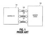
- FIG. 1illustrates one example of a typical prior art system that incorporates a flash memory 100 .
- the systemalso includes a controller 101 that is coupled to the memory device 100 .
- the controller 101is shown coupled to the memory device 100 over a data bus 105 , a control bus 106 , and an address bus 107 .
- the data buscould be a 32 bit and/or 16 bit wide double data rate (DDR) bus.
- FIG. 1shows a typical prior art system.
- FIG. 2shows a block diagram of a typical prior art implementation of a read operation.
- FIG. 3shows a timing diagram of a typical prior art command and address sequence in accordance with the embodiment of FIG. 2 .
- FIG. 4shows a timing diagram of one embodiment of a command and address sequence in accordance with the embodiment of FIG. 5 .
- FIG. 5shows a block diagram of one embodiment of an implementation of a read operation.
- FIG. 6shows a flow chart of one embodiment of a method for improving address integrity in a memory system.
- FIG. 2illustrates a block diagram of a typical prior art Joint Electron Devices Engineering Council (JEDEC) implementation of a read operation in a non-volatile memory device.
- JEDECJoint Electron Devices Engineering Council
- FIG. 2illustrates a block diagram of a typical prior art Joint Electron Devices Engineering Council (JEDEC) implementation of a read operation in a non-volatile memory device.
- JEDEC standardsprovide standardization of electronic components (e.g., non-volatile memory, controllers) so that one JEDEC-compliant memory device or controller from one manufacturer can be replaced with a similar JEDEC-compliant memory device or controller from another manufacturer. While subsequent discussions of the embodiments for improving the integrity of an address bus refer to JEDEC implementations of command, address, and data formats, the present embodiments are not limited to any one standard or format.
- the address A[n: 0 ]is divided into two parts. These two parts are subsequently referred to as row address 1 (RA 1 ) for the first part and row address 2 (RA 2 ) for the second part.
- the RA 1is stored in one of a set of row address buffers 201 that are labeled RAB 0 -RAB 3 .
- a JEDEC control signal BA[ 1 : 0 ]is a buffer select signal that selects which of the row address buffers 201 is selected to store RA 1 by controlling which output of a multiplexer 203 is connected to the input address A[n:0].
- the control signal BA[ 1 : 0 ]is active during the Pre-Active and Active time periods (as discussed subsequently with reference to FIG. 3 ) in order to select which specific page is needed to be read from the memory array 200 .
- This signalcan have one of four different states (e.g., 00, 01, 10, 11) in order to select one of the four address buffers 201 .
- the control signal BA[ 1 : 0 ]is also used to control an output multiplexer 204 that is coupled to and selects one of the outputs of the row address buffers 201 .
- Both of the first and second parts of the addressare input to the memory array 200 through another multiplexer 205 during the read operation.
- the memory array 200is also coupled to a row sensing circuit 211 that senses the state of particular memory cells that are selected in response to the two row address parts.
- the output of the row sensing circuit 211is coupled to a set of row data buffers 202 RDB 0 -RDB 3 through a multiplexer 206 that is controlled by the BA[ 1 : 0 ].
- the BA[ 1 : 0 ] signalselects into which row data buffer 202 the sensed data is input.
- the BA[ 1 : 0 ] signalis used as a control input to an output multiplexer 207 that is coupled to the outputs of the row data buffers 202 to select which of the buffer outputs is coupled to a data output multiplexer 221 .
- a double data rate (DDR) burst engine 220is coupled to the control input of the data output multiplexer 221 .
- the DDR burst engine 220uses a clock, the row address (A[n: 0 ]), and some of the configuration bits in the Mode Register Set (MRS) to control the burst output of data (DQ) from the DQ multiplexer 221 .
- MRSMode Register Set
- FIG. 3illustrates a timing diagram of a typical prior art command and address sequence in accordance with the embodiment of FIG. 2 . This figure shows what is occurring on each of the command, address, and data buses between a memory device and an external controller.
- the command businitially has a JEDEC pre-active instruction (P-ACT).
- P-ACTJEDEC pre-active instruction
- This instructioninstructs the memory device to accept the first part of the row address RA 1 that is on the address bus.
- the first part of the row addressis input to the row address buffers 201 RAB 0 -RAB 3 based on the selected bank access BA[ 1 : 0 ] signal that is on the BA bus.
- the command bushas a JEDEC active (ACT) instruction that instructs the memory device to accept the second part of the row address RA 2 that is on the address bus. Additionally during the ACT instruction, RA 2 is applied to the memory array with the first part of the row address RA 1 . The array sensing is also initiated by the ACT instruction.
- ACTJEDEC active
- the ACT instructioncan have one or more NOP instructions on the command bus. If the NOP instructions are on the command bus, the address bus is in a do not care state during this time.
- the command busthen has a read instruction (RD) that instructs the memory device to select the first page(s) of the selected row data buffer 202 RDB 0 -RDB 3 based on the selected bank access BA[ 1 : 0 ] signal that is on the BA bus.
- the selected datais output to the DQ output.
- RDread instruction
- the command busalso includes a plurality of no-operation (NOP) instructions after the read instruction RD.
- NOP instructionsare included as part of a particular JEDEC standard to increase the latency after RA 2 is transmitted over the address bus prior to the selected read data being available on the data bus to the controller.
- two NOP instructionsare used on the command bus to generate column address strobe latency of three.
- alternate embodiments that use other standardscan use more or less NOP instructions to adjust the latency.
- FIG. 3shows a plurality of read data (RD) as determined by the burst length.
- the burst lengthis the number of data words that are requested by the controller to be read.
- FIG. 3also shows a time t RCD that represents the time between the ACT instruction and the RD instruction.
- Thisis a predetermined time that is set by a particular JEDEC standard (e.g., non-volatile low power double data rate (NVM-LPDDR)) that any compliant device should respect for proper operation.
- the particular JEDEC standardallows the NOP instructions to be inserted between instructions on the command bus that adjusts the time between the ACT instruction and the RD instruction in order to meet this time specification.
- error correction code (ECC) datacan be generated by a controller (which can be any number of different transmitting devices) for a corresponding address.
- the ECC datais transmitted over the address bus, e.g., after transmitting the corresponding address, to the memory device.
- the memory devicecan then use the ECC data to correct the received address.
- FIG. 4illustrates a timing diagram wherein a NOP is used between the ACT instruction and the RD instruction, thus allowing the ECC data to be transmitted over the address bus coincident with the NOP instruction (e.g., transmitting at least a portion, and in some embodiments all, of the ECC data at a time that would be operative with respect to at least a portion, and in some embodiments all, of the NOP instruction, if the NOP instruction would have been an operative instruction; this can include, but is not limited to, for example, transmitting the ECC data and the NOP instruction at a same time).
- the ECC datacan then be used to improve the address bus integrity as described subsequently. Any method to detect and correct an error in an address pattern can be used in the present embodiments. For example, a 2 bit detection and 1 bit correction algorithm might be used to generate the ECC data.
- the use of the ECC data in a memory deviceis discussed subsequently with reference to FIG. 5 .
- FIG. 4shows that the command bus has the P-ACT instruction while the address bus has the first part of the row address (RA 1 ) and the bank access bus (BA) has the bank select signal BA[ 1 : 0 ].
- the P-ACT instructioninstructs the memory device to accept the first part of the row address RA 1 that is on the address bus.
- the command bushas the active ACT instruction that instructs the memory device to accept RA 2 that is on the address bus.
- the bank access signal BA[ 1 : 0 ]is on the BA bus.
- the array sensingis also initiated by the ACT instruction.
- a NOP instructionfollows the ACT instruction on the command bus.
- the NOP instruction on the command busallows for the ECC data to be transmitted over the address bus at the same time.
- the ECC dataincludes the error correction data for the previously transmitted address. If the address integrity feature is enabled, an internal controller 551 ( FIG. 5 ) of the memory device can accept the ECC data and store it in a register as discussed subsequently. If the address integrity feature is disabled, the ECC data can be ignored by the internal controller 551 .
- the size of the ECC datacan be dependent on the configured burst page length. In one embodiment, the size of the ECC data is at least equal to the number of the address lines. For example, for an address of 128 bits, the ECC would be at least 7 bits and an address of 256 bits would use at least 8 bits for ECC data. Alternate embodiments that use other error detection and correction algorithms could use a different size for the error correction bits.
- the address integrity featurecan be turned on or off by setting a bit in a register.
- the external controllercan transmit a control word to a mode register in a memory device that sets a bit indicating that the memory device is to accept error correction data for the address.
- an internal controller in the memory devicecan set the address integrity bit in the mode register to turn on this feature. The external controller can then read this bit indicating that the external controller should generate and/or transmit address error correction data over the address bus as shown in FIG. 4 .
- the command buscan have one or more additional NOP instructions in order to satisfy t RCD .
- the address busis in a do not care state.
- the command bushas the read instruction RD that instructs the memory device to select the first page(s) of the selected row data buffer RDB 0 -RDB 3 based on the BA[ 1 : 0 ] signal.
- the selected datais output to the DQ output.
- the command busalso includes a plurality of no-operation (NOP) instructions after the read instruction RD.
- NOP instructionsare included as part of the implemented JEDEC standard to increase the latency after RA 2 is transmitted over the address bus prior to the selected read data being available on the data bus to the controller.
- two NOP instructionsare used on the command bus to generate column address strobe latency of three.
- alternate embodiments that use other standardscan use more or fewer NOP instructions to adjust the latency.
- the selected read data(DATA 0 -DATAx) are now available on the data bus.
- FIG. 4shows a plurality of read data as determined by the burst length.
- the burst lengthis the number of data words that are requested by the controller to be read by the controller.
- the controllercan transmit a command to the memory device that sets the burst length.
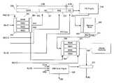
- FIG. 5illustrates a block diagram of one embodiment of a JEDEC implementation of a read operation that is implemented with the address integrity feature as illustrated in FIG. 4 .
- Alternate embodimentscan implement the address integrity feature using different standards than the JEDEC standard illustrated.
- a first part of the row address (RA 1 )is stored in one of the row address buffers 501 RAB 0 -RAB 3 .
- the address A[n: 0 ]is applied to an address multiplexer 503 that is controlled by the JEDEC control signal BA[ 1 : 0 ].
- the address multiplexer 503then accepts only RA 1 for storage in the selected row address buffer 501 RAB 0 -RAB 3 as controlled by BA[ 1 : 0 ].
- the outputs of the multiplexer 503are each coupled to a different one of the row address buffers RA 0 -RA 3 .
- a second part of the address(RA 2 ) is stored in a field 522 of an address register 550 .
- a selected one of the RA 1 addressesas selected by BA[ 1 : 0 ] from one of the row address buffers RA 0 -RA 3 through an output multiplexer 504 , is also stored in a field 521 of the address register 550 at this time.
- the memory array 500 sensing through sense circuitry 511is initiated by the ACT instruction.
- the ECC datais stored in a k-bit field 523 of the address register 550 .
- the ECC datais input to the address register 550 by the address bus A[n: 0 ]. If the address integrity feature is not enabled, the ECC field 523 can either be left empty or programmed with do not care data.
- the address register 550comprises a plurality of fields 521 - 523 comprising only RA 1 , RA 2 , and the ECC data.
- another field 520can be used in the address register 550 to increase the length of the RA 1 and RA 2 address fields 521 , 522 to an n-bit field as necessary by any particular JEDEC standard.
- the data in the extra field 520can be do not care data.
- the address register 550is coupled to an ECC engine 510 that reads the data in the address register 550 and corrects the addresses RA 1 and RA 2 as indicated by the ECC data. If the ECC data indicates that the addresses RA 1 and RA 2 do not contain one or more errors, the ECC engine 510 applies that address to the memory array 500 through a multiplexer 505 . This address is used to select particular memory cells for sensing by the row sensing circuit 511 . If the ECC data indicates that the addresses RA 1 and RA 2 contain one or more errors, the ECC engine 510 attempts to correct the address prior to applying the address to the memory array 500 .
- the memory array 500can comprise one of a plurality of technologies.
- the memory arraycan be a NOR, NAND, or PCM non-volatile memory array.
- the memory array 500can also be a volatile memory array such as dynamic random access memory.
- Other memory technologiescan also use the method for improving address integrity.
- the output of the row sensing circuit 511is input to a set of row data buffers 502 RDB 0 -RDB 3 .
- a multiplexer 506 that is controlled by the BA[ 1 : 0 ] control signaldetermines into which row data buffer RDB 0 -RDB 3 the data is stored.
- the BA[ 1 : 0 ] signalis used as a control input to an output multiplexer 507 that is coupled to the outputs of the row data buffers 502 to select which of the buffer outputs is coupled to a data output multiplexer 531 .
- a double data rate (DDR) burst engine 530is coupled to the control input of the data output multiplexer 531 .
- the DDR burst engine 530uses a clock, the row address (A[n: 0 ]), and some configuration bits in the Mode Register Set (MRS) to control the burst output of data (DQ) from the data output multiplexer 531 .
- the external controllercan set the burst length and rate by setting particular bits in a register such as the MRS register.
- FIG. 6illustrates a flow chart of one embodiment of a method for improving address integrity in a memory system.
- the external controllerdetermines if the address integrity feature is enabled 601 . This can be accomplished by reading a mode register in the memory device that has an address integrity bit. In one embodiment, when this bit is set to a logical 1, the address integrity feature is enabled and when the bit is set to a logical 0, the address integrity feature is disabled.
- the external controllerIf the address integrity feature is enabled, the external controller generates error correction code (e.g., error correction data, ECC data) for the transmitted address 606 .
- error correction codee.g., error correction data, ECC data
- the external controllertransmits the P-ACT command over the command bus coincident with transmitting the row address over the address bus 607 .
- the ACT commandis then transmitted over the command bus coincident with transmitting RA 2 over the address bus 609 .
- a NOP instructionis then transmitted over the command bus coincident with the ECC data, generated for the address previously transmitted over the address bus 611 .
- the methodcould continue by determining if t RCD has been met 613 . If not, NOP instructions are transmitted with “Do Not Care” data 620 . If t RCD has been met 613 , the external controller transmits a read instruction to the memory device over the command bus 614 .
- the read instructioncan be followed by one or more NOP instructions depending on the CAS latency required by the implemented standard.
- the memory devicecan then transmit the burst of data to the external controller over the data bus and the external controller receives the data 615 .
- the addresscan be transmitted without the ECC data 603 .
- the NOP instructionis also not transmitted over the command bus.
- the NOP instructionis transmitted over the command bus and the ECC data is transmitted over the address bus but the memory device ignores the ECC data.
- the P-ACT and ACT commandsare commands associated with a particular JEDEC implementation of a standard. Alternate embodiments may not use such commands, depending on the standard being implemented, but can still transmit a NOP instruction over the command bus coincident with ECC data over the address bus.
- one or more embodimentsinclude a selectable address integrity feature that can improve the integrity of an address bus in a memory system.
- the controllergenerates error correction data corresponding to an address.
- the error correction datacan be transmitted to the memory device over the address bus coincident with transmitting a NOP instruction over the command bus.
Landscapes
- Engineering & Computer Science (AREA)
- Theoretical Computer Science (AREA)
- Physics & Mathematics (AREA)
- General Engineering & Computer Science (AREA)
- General Physics & Mathematics (AREA)
- Quality & Reliability (AREA)
- Human Computer Interaction (AREA)
- Computer Security & Cryptography (AREA)
- Techniques For Improving Reliability Of Storages (AREA)
- Dram (AREA)
Abstract
Description
Claims (33)
Priority Applications (8)
| Application Number | Priority Date | Filing Date | Title |
|---|---|---|---|
| US13/490,633US9009570B2 (en) | 2012-06-07 | 2012-06-07 | Integrity of an address bus |
| CN201710761680.2ACN107608816B (en) | 2012-06-07 | 2013-06-04 | Improving integrity of an address bus |
| KR1020157000386AKR101651384B1 (en) | 2012-06-07 | 2013-06-04 | Improving integrity of an address bus |
| EP13800122.7AEP2859451B1 (en) | 2012-06-07 | 2013-06-04 | Improving integrity of an address bus |
| PCT/US2013/044061WO2013184651A1 (en) | 2012-06-07 | 2013-06-04 | Improving integrity of an address bus |
| JP2015516114AJP5955459B2 (en) | 2012-06-07 | 2013-06-04 | Improved address bus integrity |
| CN201380037117.0ACN104428756B (en) | 2012-06-07 | 2013-06-04 | Improves address bus integrity |
| US14/620,474US9557926B2 (en) | 2012-06-07 | 2015-02-12 | Integrity of an address bus |
Applications Claiming Priority (1)
| Application Number | Priority Date | Filing Date | Title |
|---|---|---|---|
| US13/490,633US9009570B2 (en) | 2012-06-07 | 2012-06-07 | Integrity of an address bus |
Related Child Applications (1)
| Application Number | Title | Priority Date | Filing Date |
|---|---|---|---|
| US14/620,474ContinuationUS9557926B2 (en) | 2012-06-07 | 2015-02-12 | Integrity of an address bus |
Publications (2)
| Publication Number | Publication Date |
|---|---|
| US20130332783A1 US20130332783A1 (en) | 2013-12-12 |
| US9009570B2true US9009570B2 (en) | 2015-04-14 |
Family
ID=49712541
Family Applications (2)
| Application Number | Title | Priority Date | Filing Date |
|---|---|---|---|
| US13/490,633Active2032-09-21US9009570B2 (en) | 2012-06-07 | 2012-06-07 | Integrity of an address bus |
| US14/620,474ActiveUS9557926B2 (en) | 2012-06-07 | 2015-02-12 | Integrity of an address bus |
Family Applications After (1)
| Application Number | Title | Priority Date | Filing Date |
|---|---|---|---|
| US14/620,474ActiveUS9557926B2 (en) | 2012-06-07 | 2015-02-12 | Integrity of an address bus |
Country Status (6)
| Country | Link |
|---|---|
| US (2) | US9009570B2 (en) |
| EP (1) | EP2859451B1 (en) |
| JP (1) | JP5955459B2 (en) |
| KR (1) | KR101651384B1 (en) |
| CN (2) | CN104428756B (en) |
| WO (1) | WO2013184651A1 (en) |
Cited By (2)
| Publication number | Priority date | Publication date | Assignee | Title |
|---|---|---|---|---|
| US20170153945A1 (en)* | 2015-12-01 | 2017-06-01 | Nvidia Corporation | Memory management systems and methods |
| US12340088B2 (en) | 2023-02-28 | 2025-06-24 | Samsung Electronics Co., Ltd. | Memory device, memory control device and operating method of memory device for checking command and address (CA) signal with predetermined pattern of command |
Families Citing this family (4)
| Publication number | Priority date | Publication date | Assignee | Title |
|---|---|---|---|---|
| US10585817B2 (en) | 2018-05-29 | 2020-03-10 | Seagate Technology Llc | Method of signal integrity and power integrity analysis for address bus |
| US11144385B2 (en) | 2018-08-21 | 2021-10-12 | Micron Technology, Inc. | Transmission failure feedback schemes for reducing crosstalk |
| US11450394B2 (en) | 2019-09-11 | 2022-09-20 | SK Hynix Inc. | Controller and operating method thereof |
| US11507453B2 (en)* | 2020-10-20 | 2022-11-22 | Micron Technology, Inc. | Low-latency register error correction |
Citations (24)
| Publication number | Priority date | Publication date | Assignee | Title |
|---|---|---|---|---|
| US4214303A (en)* | 1977-12-22 | 1980-07-22 | Honeywell Information Systems Inc. | Word oriented high speed buffer memory system connected to a system bus |
| US4672614A (en)* | 1983-12-21 | 1987-06-09 | Nec Corporation | Semiconductor memory device with parallel addressing and data-correcting functions |
| US4799222A (en)* | 1987-01-07 | 1989-01-17 | Honeywell Bull Inc. | Address transform method and apparatus for transferring addresses |
| US5678020A (en) | 1994-01-04 | 1997-10-14 | Intel Corporation | Memory subsystem wherein a single processor chip controls multiple cache memory chips |
| US20050114750A1 (en)* | 2003-11-25 | 2005-05-26 | International Business Machines Corporation | High reliability memory subsystem using data error correcting code symbol sliced command repowering |
| US20050125708A1 (en)* | 2003-12-04 | 2005-06-09 | Texas Instruments Incorporated | Method for streamlining error connection code computation while reading or programming a NAND flash memory |
| US6912616B2 (en)* | 2002-11-12 | 2005-06-28 | Hewlett-Packard Development Company, L.P. | Mapping addresses to memory banks based on at least one mathematical relationship |
| US6931576B2 (en) | 2002-01-07 | 2005-08-16 | Sun Microsystems, Inc. | Data integrity device providing heightened error protection in a data processing system |
| US7026850B2 (en)* | 2001-05-21 | 2006-04-11 | Acuid Corporation Limited | Programmable self-calibrating vernier and method |
| US20060203601A1 (en)* | 2004-08-16 | 2006-09-14 | Pawlowski J T | Memory device and method having programmable address configurations |
| US20070088921A1 (en)* | 2005-10-13 | 2007-04-19 | Joon-Kun Kim | Semiconductor memory devices including mode registers and systems including the same |
| US20070133315A1 (en)* | 2005-11-29 | 2007-06-14 | Kang Uk-Song | Dynamic random access memory device and associated refresh cycle |
| US20070250756A1 (en) | 2003-04-14 | 2007-10-25 | Gower Kevin C | High reliability memory module with a fault tolerant address and command bus |
| US7293221B1 (en)* | 2004-01-27 | 2007-11-06 | Sun Microsystems, Inc. | Methods and systems for detecting memory address transfer errors in an address bus |
| US20080168331A1 (en) | 2007-01-05 | 2008-07-10 | Thomas Vogelsang | Memory including error correction code circuit |
| US20090013233A1 (en)* | 2007-07-06 | 2009-01-08 | Micron Technology, Inc. | Error recovery storage along a nand-flash string |
| US7571297B2 (en) | 2005-12-30 | 2009-08-04 | Intel Corporation | Data invalid signal for non-deterministic latency in a memory system |
| US20090271678A1 (en) | 2008-04-25 | 2009-10-29 | Andreas Schneider | Interface voltage adjustment based on error detection |
| US7694196B2 (en) | 2007-11-20 | 2010-04-06 | Qimonda North America Corp. | Self-diagnostic scheme for detecting errors |
| US7804735B2 (en) | 2008-02-29 | 2010-09-28 | Qualcomm Incorporated | Dual channel memory architecture having a reduced interface pin requirements using a double data rate scheme for the address/control signals |
| US20100318718A1 (en) | 2009-06-11 | 2010-12-16 | Sean Eilert | Memory device for a hierarchical memory architecture |
| US7937631B2 (en) | 2007-08-28 | 2011-05-03 | Qimonda Ag | Method for self-test and self-repair in a multi-chip package environment |
| US8135935B2 (en) | 2007-03-20 | 2012-03-13 | Advanced Micro Devices, Inc. | ECC implementation in non-ECC components |
| US20120246542A1 (en)* | 2011-03-22 | 2012-09-27 | Freescale Semiconductor, Inc. | Selective checkbit modification for error correction |
Family Cites Families (16)
| Publication number | Priority date | Publication date | Assignee | Title |
|---|---|---|---|---|
| JPH07105102A (en)* | 1993-10-08 | 1995-04-21 | Toshiba Corp | Memory control unit |
| JP2000066962A (en)* | 1998-08-25 | 2000-03-03 | Hitachi Ltd | Storage device |
| US6775759B2 (en)* | 2001-12-07 | 2004-08-10 | Micron Technology, Inc. | Sequential nibble burst ordering for data |
| US6941493B2 (en)* | 2002-02-27 | 2005-09-06 | Sun Microsystems, Inc. | Memory subsystem including an error detection mechanism for address and control signals |
| CN100535933C (en)* | 2004-02-03 | 2009-09-02 | 松下电器产业株式会社 | Memory card, data processor, memory card control method and memory card setting method |
| KR100604836B1 (en)* | 2004-02-26 | 2006-07-26 | 삼성전자주식회사 | Memory system employing simultaneous bidirectional I / O circuits on address bus lines |
| JP2006139498A (en)* | 2004-11-11 | 2006-06-01 | Fujitsu Ltd | Control device |
| US7464241B2 (en) | 2004-11-22 | 2008-12-09 | Intel Corporation | Memory transaction burst operation and memory components supporting temporally multiplexed error correction coding |
| US20060156191A1 (en)* | 2005-01-07 | 2006-07-13 | Steve Driediger | Memory addressing error protection systems and methods |
| US7802169B2 (en)* | 2005-12-12 | 2010-09-21 | Mediatek Inc. | Error correction devices and correction methods |
| US8352805B2 (en)* | 2006-05-18 | 2013-01-08 | Rambus Inc. | Memory error detection |
| JP4470183B2 (en)* | 2006-08-28 | 2010-06-02 | エルピーダメモリ株式会社 | Semiconductor memory device |
| JP2008090442A (en)* | 2006-09-29 | 2008-04-17 | Fujitsu Ltd | Memory control device |
| US7477522B2 (en)* | 2006-10-23 | 2009-01-13 | International Business Machines Corporation | High density high reliability memory module with a fault tolerant address and command bus |
| US8307180B2 (en)* | 2008-02-28 | 2012-11-06 | Nokia Corporation | Extended utilization area for a memory device |
| JP5554476B2 (en)* | 2008-06-23 | 2014-07-23 | ピーエスフォー ルクスコ エスエイアールエル | Semiconductor memory device and method for testing semiconductor memory device |
- 2012
- 2012-06-07USUS13/490,633patent/US9009570B2/enactiveActive
- 2013
- 2013-06-04CNCN201380037117.0Apatent/CN104428756B/enactiveActive
- 2013-06-04JPJP2015516114Apatent/JP5955459B2/enactiveActive
- 2013-06-04KRKR1020157000386Apatent/KR101651384B1/enactiveActive
- 2013-06-04CNCN201710761680.2Apatent/CN107608816B/enactiveActive
- 2013-06-04EPEP13800122.7Apatent/EP2859451B1/enactiveActive
- 2013-06-04WOPCT/US2013/044061patent/WO2013184651A1/enactiveApplication Filing
- 2015
- 2015-02-12USUS14/620,474patent/US9557926B2/enactiveActive
Patent Citations (24)
| Publication number | Priority date | Publication date | Assignee | Title |
|---|---|---|---|---|
| US4214303A (en)* | 1977-12-22 | 1980-07-22 | Honeywell Information Systems Inc. | Word oriented high speed buffer memory system connected to a system bus |
| US4672614A (en)* | 1983-12-21 | 1987-06-09 | Nec Corporation | Semiconductor memory device with parallel addressing and data-correcting functions |
| US4799222A (en)* | 1987-01-07 | 1989-01-17 | Honeywell Bull Inc. | Address transform method and apparatus for transferring addresses |
| US5678020A (en) | 1994-01-04 | 1997-10-14 | Intel Corporation | Memory subsystem wherein a single processor chip controls multiple cache memory chips |
| US7026850B2 (en)* | 2001-05-21 | 2006-04-11 | Acuid Corporation Limited | Programmable self-calibrating vernier and method |
| US6931576B2 (en) | 2002-01-07 | 2005-08-16 | Sun Microsystems, Inc. | Data integrity device providing heightened error protection in a data processing system |
| US6912616B2 (en)* | 2002-11-12 | 2005-06-28 | Hewlett-Packard Development Company, L.P. | Mapping addresses to memory banks based on at least one mathematical relationship |
| US20070250756A1 (en) | 2003-04-14 | 2007-10-25 | Gower Kevin C | High reliability memory module with a fault tolerant address and command bus |
| US20050114750A1 (en)* | 2003-11-25 | 2005-05-26 | International Business Machines Corporation | High reliability memory subsystem using data error correcting code symbol sliced command repowering |
| US20050125708A1 (en)* | 2003-12-04 | 2005-06-09 | Texas Instruments Incorporated | Method for streamlining error connection code computation while reading or programming a NAND flash memory |
| US7293221B1 (en)* | 2004-01-27 | 2007-11-06 | Sun Microsystems, Inc. | Methods and systems for detecting memory address transfer errors in an address bus |
| US20060203601A1 (en)* | 2004-08-16 | 2006-09-14 | Pawlowski J T | Memory device and method having programmable address configurations |
| US20070088921A1 (en)* | 2005-10-13 | 2007-04-19 | Joon-Kun Kim | Semiconductor memory devices including mode registers and systems including the same |
| US20070133315A1 (en)* | 2005-11-29 | 2007-06-14 | Kang Uk-Song | Dynamic random access memory device and associated refresh cycle |
| US7571297B2 (en) | 2005-12-30 | 2009-08-04 | Intel Corporation | Data invalid signal for non-deterministic latency in a memory system |
| US20080168331A1 (en) | 2007-01-05 | 2008-07-10 | Thomas Vogelsang | Memory including error correction code circuit |
| US8135935B2 (en) | 2007-03-20 | 2012-03-13 | Advanced Micro Devices, Inc. | ECC implementation in non-ECC components |
| US20090013233A1 (en)* | 2007-07-06 | 2009-01-08 | Micron Technology, Inc. | Error recovery storage along a nand-flash string |
| US7937631B2 (en) | 2007-08-28 | 2011-05-03 | Qimonda Ag | Method for self-test and self-repair in a multi-chip package environment |
| US7694196B2 (en) | 2007-11-20 | 2010-04-06 | Qimonda North America Corp. | Self-diagnostic scheme for detecting errors |
| US7804735B2 (en) | 2008-02-29 | 2010-09-28 | Qualcomm Incorporated | Dual channel memory architecture having a reduced interface pin requirements using a double data rate scheme for the address/control signals |
| US20090271678A1 (en) | 2008-04-25 | 2009-10-29 | Andreas Schneider | Interface voltage adjustment based on error detection |
| US20100318718A1 (en) | 2009-06-11 | 2010-12-16 | Sean Eilert | Memory device for a hierarchical memory architecture |
| US20120246542A1 (en)* | 2011-03-22 | 2012-09-27 | Freescale Semiconductor, Inc. | Selective checkbit modification for error correction |
Non-Patent Citations (2)
| Title |
|---|
| JEDEC, "Low Power Double Data Rate (LPDDR) Non-Volatile Memory (NVM) Specification", Arlington, VA, Jan. 2007, 70 pgs. |
| JEDEC, "LPDDR-NVM Memory Standard", Arlington, VA, Nov. 29, 2007, 2 pgs. |
Cited By (4)
| Publication number | Priority date | Publication date | Assignee | Title |
|---|---|---|---|---|
| US20170153945A1 (en)* | 2015-12-01 | 2017-06-01 | Nvidia Corporation | Memory management systems and methods |
| US10528423B2 (en)* | 2015-12-01 | 2020-01-07 | Nvidia Corporation | Memory management systems and methods |
| US11256568B2 (en) | 2015-12-01 | 2022-02-22 | Nvidia Corporation | Memory management systems and methods |
| US12340088B2 (en) | 2023-02-28 | 2025-06-24 | Samsung Electronics Co., Ltd. | Memory device, memory control device and operating method of memory device for checking command and address (CA) signal with predetermined pattern of command |
Also Published As
| Publication number | Publication date |
|---|---|
| JP2015518994A (en) | 2015-07-06 |
| CN104428756B (en) | 2017-10-13 |
| CN107608816A (en) | 2018-01-19 |
| US20150160874A1 (en) | 2015-06-11 |
| US9557926B2 (en) | 2017-01-31 |
| KR101651384B1 (en) | 2016-08-25 |
| US20130332783A1 (en) | 2013-12-12 |
| KR20150029686A (en) | 2015-03-18 |
| EP2859451A1 (en) | 2015-04-15 |
| WO2013184651A1 (en) | 2013-12-12 |
| JP5955459B2 (en) | 2016-07-20 |
| EP2859451A4 (en) | 2015-12-23 |
| EP2859451B1 (en) | 2019-12-18 |
| CN104428756A (en) | 2015-03-18 |
| CN107608816B (en) | 2021-06-01 |
Similar Documents
| Publication | Publication Date | Title |
|---|---|---|
| US10152373B2 (en) | Methods of operating memory including receipt of ECC data | |
| US11681579B2 (en) | Semiconductor memory devices and memory systems including the same | |
| US11194657B2 (en) | Semiconductor memory devices, memory systems, and methods of operating the semiconductor memory devices | |
| CN111986727B (en) | Semiconductor memory device and method of operating the same | |
| US10503589B2 (en) | Semiconductor memory devices, memory systems and methods of operating semiconductor memory devices | |
| US9557926B2 (en) | Integrity of an address bus | |
| US10049006B2 (en) | Controller-based memory scrub for DRAMs with internal error-correcting code (ECC) bits contemporaneously during auto refresh or by using masked write commands | |
| US10614906B2 (en) | Semiconductor memory devices, memory systems and methods of operating semiconductor memory devices | |
| KR20190137281A (en) | Semiconductor memory devices, memory systems including the same and method of operating semiconductor memory devices | |
| US20080168331A1 (en) | Memory including error correction code circuit | |
| US7571276B2 (en) | Read operation for semiconductor memory devices | |
| US10613931B2 (en) | Memory devices | |
| KR100721021B1 (en) | Burst read circuit and burst data output method of semiconductor memory device | |
| CN110942798A (en) | Semiconductor memory device, memory system, and method of operating a semiconductor memory device | |
| US9564207B2 (en) | Semiconductor memory device, semiconductor memory system and method for controlling self refresh cycle thereof | |
| US20250245099A1 (en) | Apparatuses and methods to perform self-scrub operations at a memory |
Legal Events
| Date | Code | Title | Description |
|---|---|---|---|
| AS | Assignment | Owner name:MICRON TECHNOLOGY, INC., IDAHO Free format text:ASSIGNMENT OF ASSIGNORS INTEREST;ASSIGNOR:TROIA, ALBERTO;REEL/FRAME:028334/0331 Effective date:20120517 | |
| FEPP | Fee payment procedure | Free format text:PAYOR NUMBER ASSIGNED (ORIGINAL EVENT CODE: ASPN); ENTITY STATUS OF PATENT OWNER: LARGE ENTITY | |
| STCF | Information on status: patent grant | Free format text:PATENTED CASE | |
| AS | Assignment | Owner name:U.S. BANK NATIONAL ASSOCIATION, AS COLLATERAL AGENT, CALIFORNIA Free format text:SECURITY INTEREST;ASSIGNOR:MICRON TECHNOLOGY, INC.;REEL/FRAME:038669/0001 Effective date:20160426 Owner name:U.S. BANK NATIONAL ASSOCIATION, AS COLLATERAL AGEN Free format text:SECURITY INTEREST;ASSIGNOR:MICRON TECHNOLOGY, INC.;REEL/FRAME:038669/0001 Effective date:20160426 | |
| AS | Assignment | Owner name:MORGAN STANLEY SENIOR FUNDING, INC., AS COLLATERAL AGENT, MARYLAND Free format text:PATENT SECURITY AGREEMENT;ASSIGNOR:MICRON TECHNOLOGY, INC.;REEL/FRAME:038954/0001 Effective date:20160426 Owner name:MORGAN STANLEY SENIOR FUNDING, INC., AS COLLATERAL Free format text:PATENT SECURITY AGREEMENT;ASSIGNOR:MICRON TECHNOLOGY, INC.;REEL/FRAME:038954/0001 Effective date:20160426 | |
| AS | Assignment | Owner name:U.S. BANK NATIONAL ASSOCIATION, AS COLLATERAL AGENT, CALIFORNIA Free format text:CORRECTIVE ASSIGNMENT TO CORRECT THE REPLACE ERRONEOUSLY FILED PATENT #7358718 WITH THE CORRECT PATENT #7358178 PREVIOUSLY RECORDED ON REEL 038669 FRAME 0001. ASSIGNOR(S) HEREBY CONFIRMS THE SECURITY INTEREST;ASSIGNOR:MICRON TECHNOLOGY, INC.;REEL/FRAME:043079/0001 Effective date:20160426 Owner name:U.S. BANK NATIONAL ASSOCIATION, AS COLLATERAL AGEN Free format text:CORRECTIVE ASSIGNMENT TO CORRECT THE REPLACE ERRONEOUSLY FILED PATENT #7358718 WITH THE CORRECT PATENT #7358178 PREVIOUSLY RECORDED ON REEL 038669 FRAME 0001. ASSIGNOR(S) HEREBY CONFIRMS THE SECURITY INTEREST;ASSIGNOR:MICRON TECHNOLOGY, INC.;REEL/FRAME:043079/0001 Effective date:20160426 | |
| AS | Assignment | Owner name:JPMORGAN CHASE BANK, N.A., AS COLLATERAL AGENT, ILLINOIS Free format text:SECURITY INTEREST;ASSIGNORS:MICRON TECHNOLOGY, INC.;MICRON SEMICONDUCTOR PRODUCTS, INC.;REEL/FRAME:047540/0001 Effective date:20180703 Owner name:JPMORGAN CHASE BANK, N.A., AS COLLATERAL AGENT, IL Free format text:SECURITY INTEREST;ASSIGNORS:MICRON TECHNOLOGY, INC.;MICRON SEMICONDUCTOR PRODUCTS, INC.;REEL/FRAME:047540/0001 Effective date:20180703 | |
| AS | Assignment | Owner name:MICRON TECHNOLOGY, INC., IDAHO Free format text:RELEASE BY SECURED PARTY;ASSIGNOR:U.S. BANK NATIONAL ASSOCIATION, AS COLLATERAL AGENT;REEL/FRAME:047243/0001 Effective date:20180629 | |
| MAFP | Maintenance fee payment | Free format text:PAYMENT OF MAINTENANCE FEE, 4TH YEAR, LARGE ENTITY (ORIGINAL EVENT CODE: M1551); ENTITY STATUS OF PATENT OWNER: LARGE ENTITY Year of fee payment:4 | |
| AS | Assignment | Owner name:MICRON TECHNOLOGY, INC., IDAHO Free format text:RELEASE BY SECURED PARTY;ASSIGNOR:MORGAN STANLEY SENIOR FUNDING, INC., AS COLLATERAL AGENT;REEL/FRAME:050937/0001 Effective date:20190731 | |
| AS | Assignment | Owner name:MICRON SEMICONDUCTOR PRODUCTS, INC., IDAHO Free format text:RELEASE BY SECURED PARTY;ASSIGNOR:JPMORGAN CHASE BANK, N.A., AS COLLATERAL AGENT;REEL/FRAME:051028/0001 Effective date:20190731 Owner name:MICRON TECHNOLOGY, INC., IDAHO Free format text:RELEASE BY SECURED PARTY;ASSIGNOR:JPMORGAN CHASE BANK, N.A., AS COLLATERAL AGENT;REEL/FRAME:051028/0001 Effective date:20190731 | |
| MAFP | Maintenance fee payment | Free format text:PAYMENT OF MAINTENANCE FEE, 8TH YEAR, LARGE ENTITY (ORIGINAL EVENT CODE: M1552); ENTITY STATUS OF PATENT OWNER: LARGE ENTITY Year of fee payment:8 |