US9009375B2 - Sharing of bypassed I/O transaction information - Google Patents
Sharing of bypassed I/O transaction informationDownload PDFInfo
- Publication number
- US9009375B2 US9009375B2US13/927,343US201313927343AUS9009375B2US 9009375 B2US9009375 B2US 9009375B2US 201313927343 AUS201313927343 AUS 201313927343AUS 9009375 B2US9009375 B2US 9009375B2
- Authority
- US
- United States
- Prior art keywords
- requests
- storage devices
- storage controller
- storage
- host system
- Prior art date
- Legal status (The legal status is an assumption and is not a legal conclusion. Google has not performed a legal analysis and makes no representation as to the accuracy of the status listed.)
- Expired - Fee Related, expires
Links
Images


Classifications
- G—PHYSICS
- G06—COMPUTING OR CALCULATING; COUNTING
- G06F—ELECTRIC DIGITAL DATA PROCESSING
- G06F3/00—Input arrangements for transferring data to be processed into a form capable of being handled by the computer; Output arrangements for transferring data from processing unit to output unit, e.g. interface arrangements
- G06F3/06—Digital input from, or digital output to, record carriers, e.g. RAID, emulated record carriers or networked record carriers
- G06F3/0601—Interfaces specially adapted for storage systems
- G06F3/0628—Interfaces specially adapted for storage systems making use of a particular technique
- G06F3/0655—Vertical data movement, i.e. input-output transfer; data movement between one or more hosts and one or more storage devices
- G—PHYSICS
- G06—COMPUTING OR CALCULATING; COUNTING
- G06F—ELECTRIC DIGITAL DATA PROCESSING
- G06F3/00—Input arrangements for transferring data to be processed into a form capable of being handled by the computer; Output arrangements for transferring data from processing unit to output unit, e.g. interface arrangements
- G06F3/06—Digital input from, or digital output to, record carriers, e.g. RAID, emulated record carriers or networked record carriers
- G06F3/0601—Interfaces specially adapted for storage systems
- G06F3/0602—Interfaces specially adapted for storage systems specifically adapted to achieve a particular effect
- G06F3/061—Improving I/O performance
- G—PHYSICS
- G06—COMPUTING OR CALCULATING; COUNTING
- G06F—ELECTRIC DIGITAL DATA PROCESSING
- G06F3/00—Input arrangements for transferring data to be processed into a form capable of being handled by the computer; Output arrangements for transferring data from processing unit to output unit, e.g. interface arrangements
- G06F3/06—Digital input from, or digital output to, record carriers, e.g. RAID, emulated record carriers or networked record carriers
- G06F3/0601—Interfaces specially adapted for storage systems
- G06F3/0628—Interfaces specially adapted for storage systems making use of a particular technique
- G06F3/0655—Vertical data movement, i.e. input-output transfer; data movement between one or more hosts and one or more storage devices
- G06F3/0656—Data buffering arrangements
- G—PHYSICS
- G06—COMPUTING OR CALCULATING; COUNTING
- G06F—ELECTRIC DIGITAL DATA PROCESSING
- G06F3/00—Input arrangements for transferring data to be processed into a form capable of being handled by the computer; Output arrangements for transferring data from processing unit to output unit, e.g. interface arrangements
- G06F3/06—Digital input from, or digital output to, record carriers, e.g. RAID, emulated record carriers or networked record carriers
- G06F3/0601—Interfaces specially adapted for storage systems
- G06F3/0628—Interfaces specially adapted for storage systems making use of a particular technique
- G06F3/0655—Vertical data movement, i.e. input-output transfer; data movement between one or more hosts and one or more storage devices
- G06F3/0659—Command handling arrangements, e.g. command buffers, queues, command scheduling
- G—PHYSICS
- G06—COMPUTING OR CALCULATING; COUNTING
- G06F—ELECTRIC DIGITAL DATA PROCESSING
- G06F3/00—Input arrangements for transferring data to be processed into a form capable of being handled by the computer; Output arrangements for transferring data from processing unit to output unit, e.g. interface arrangements
- G06F3/06—Digital input from, or digital output to, record carriers, e.g. RAID, emulated record carriers or networked record carriers
- G06F3/0601—Interfaces specially adapted for storage systems
- G06F3/0668—Interfaces specially adapted for storage systems adopting a particular infrastructure
- G06F3/0671—In-line storage system
- G06F3/0683—Plurality of storage devices
- G06F3/0689—Disk arrays, e.g. RAID, JBOD
- G—PHYSICS
- G06—COMPUTING OR CALCULATING; COUNTING
- G06F—ELECTRIC DIGITAL DATA PROCESSING
- G06F11/00—Error detection; Error correction; Monitoring
- G06F11/07—Responding to the occurrence of a fault, e.g. fault tolerance
- G06F11/08—Error detection or correction by redundancy in data representation, e.g. by using checking codes
- G06F11/10—Adding special bits or symbols to the coded information, e.g. parity check, casting out 9's or 11's
- G06F11/1076—Parity data used in redundant arrays of independent storages, e.g. in RAID systems
Definitions
- RAID arraysmay be configured in ways that provide redundancy and error recovery without any loss of data. RAID arrays may also be configured to increase read and write performance by allowing data to be read or written simultaneously to multiple disk drives. RAID arrays may also be configured to allow “hot-swapping” which allows a failed disk to be replaced without interrupting the storage services of the array.
- the 1987 publication by David A. Patterson, et al., from the University of California at Berkeley titled “A Case for Redundant Arrays of Inexpensive Disks (RAID)”discusses the fundamental concepts and levels of RAID technology.
- RAID storage systemstypically utilize a controller that shields the user or host system from the details of managing the storage array.
- the controllermakes the storage array appear as one or more disk drives (or volumes). This is accomplished in spite of the fact that the data (or redundant data) for a particular volume may be spread across multiple disk drives.
- An embodiment of the inventionmay therefore comprise a method of operating a storage system, comprising: sending a first I/O transaction request to a storage controller for processing by firmware running on the storage controller; sending a second I/O transaction request to storage hardware without further processing by the firmware running on the storage controller; and, storing information associated with the second I/O transaction in a circular buffer.
- An embodiment of the inventionmay therefore further comprise a storage system, comprising: a storage controller configured with a circular buffer to receive information associated with I/O transactions that are not sent to be processed by storage controller firmware; and, a host system running a storage driver configured to send a first plurality of I/O transactions directly to storage hardware without sending the first plurality of I/O transactions to be processed by storage controller firmware.
- the storage driveralso configured to send a second plurality of I/O transactions to the storage controller for processing by the storage controller firmware.
- the storage driveralso configured to send information associated with the first plurality of I/O transactions to the circular buffer.
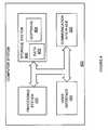
- FIG. 1is a block diagram illustrating a storage system.
- FIG. 2is an illustration of an I/O path.
- FIG. 3is a flowchart illustrating a method of operating a storage system.
- FIG. 4is a block diagram of a computer system.
- FIG. 1is a block diagram illustrating a storage system.
- storage system 100comprises host processor 110 , bus 120 , storage controller 130 , and storage devices 141 - 143 .
- Host processor 110includes driver 111 .
- Storage controller 130includes message unit 132 , processor 134 , I/O accelerator (IOA) 136 , serial attached SCSI (SAS) interface 138 , and circular buffer 139 .
- I/O acceleratorI/O accelerator
- SASserial attached SCSI
- Processor 134includes firmware 135 .
- Bus 120is operatively coupled to bus 120 .
- Bus 120may be, for example, a PCIe bus.
- Bus 120is operatively coupled to storage controller 130 .
- Storage controller 130may be, or include, a RAID controller.
- Message unit 132is operatively coupled to processor 134 and I/O accelerator 136 .
- I/O accelerator 136is operatively coupled to SAS interface 138 and processor 134 .
- Processor 134is operatively coupled to SAS interface 138 .
- SAS interface 138is operatively coupled to storage devices 141 - 143 .
- Storage devices 141 - 143may be, for example, physical disk drives, solid-state disk drives, or a combination thereof.
- Circular buffer 139can be established in storage controller 130 memory space. Circular buffer 139 can be accessible to driver 111 using bus 120 address space.
- Host processorruns (executes) driver 111 .
- Processor 134runs firmware 135 .
- Driver 111 and firmware 135may cooperate to provide storage and/or RAID functionality to host processor 110 .
- host processor 110may access one or more of storage devices 141 - 143 via storage controller 130 using driver 111 .
- Storage devices 141 - 143may be configured by storage controller 130 by running firmware 135 .
- Storage controller 130may operate one or more of storage devices 141 - 143 as a RAID array.
- Storage controller 130may operate one or more of storage devices 141 - 143 to appear to host process 100 as one or more virtual volumes (a.k.a., virtual disks).
- storage controller 130can support multiple paths for I/O transactions to proceed to/from host processor 110 to/from storage devices 141 - 143 . Some of these paths may have higher performance than others.
- message unit 132may be configured to receive an I/O transaction request from host processor 110 via bus 120 . Message unit 132 may process this I/O transaction request and then pass the I/O transaction request to processor 134 for further processing. This further processing may be controlled and/or instructed by firmware 135 .
- This further processingmay be or include processing to implement a RAID level on storage devices 141 - 143 .
- This further processingmay be or include processing to implement caching of data stored on one or more of storage devices 141 - 143 .
- Caching strategies that may be implementedare, for example, writeback, write-through, etc.
- RAID levelsthat may be implemented include, for example, RAID levels 0-6 (and combinations thereof), etc.
- message unit 132may be configured to receive I/O transaction requests from host processor 110 via bus 120 and pass these I/O requests to I/O accelerator 136 and then on to SAS interface 138 for passing to storage devices 141 - 143 without further processing by processor 134 and/or firmware 135 .
- Message unit 132 and/or I/O accelerator 136may be configured by driver 111 to pass I/O transaction requests directly to storage devices 141 - 143 without further processing by processor 134 and/or firmware 135 .
- Sending I/O transactions directly to storage devices 141 - 143 without processing by processor 134provides a high performance I/O transaction path from host 110 to storage devices 141 - 143 .
- driver 111can store, in circular buffer 139 , information about I/O transactions that are sent directly to storage devices 141 - 143 . This is illustrated in FIG. 2 by arrow 251 .
- Driver 111can continuously store information in buffer 139 about I/O transactions that have been sent directly to storage devices 141 - 143 .
- driver 111may also continuously store information in buffer 139 about I/O transactions that have not been sent directly to storage devices 141 - 143 .
- Driver 111may store include logical unit number (LUN), LBA, count, and operation performed (e.g., read or write).
- LUNlogical unit number
- LBAlogical unit number
- counte.g., count
- operation performede.g., read or write.
- Driver 111may place information in buffer 139 without acknowledgement that firmware 134 has or will, use the information in buffer 139 .
- Driver 111may place information in circular buffer 139 that overwrites information previously stored in buffer 139 .
- IOA 136can store, in circular buffer 139 , information about I/O transactions that are sent directly to storage devices 141 - 143 .
- IOA 136can continuously store information in buffer 139 about I/O transactions that have been sent directly to storage devices 141 - 143 .
- IOA 136may also continuously store information in buffer 139 about I/O transactions that have not been sent directly to storage devices 141 - 143 .
- Information that IOA 136may store include logical unit number (LUN), LBA, count, and operation performed (e.g., read or write).
- IOA 136may place information in buffer 139 without acknowledgement that firmware 134 has or will, use the information in buffer 139 .
- IOA 136may place information in circular buffer 139 that overwrites information previously stored in buffer 139 .
- Firmware 135 running on processor 134can read the information in circular buffer 139 .
- Firmware 135can use the information in circular buffer 139 to, for example, determine if certain storage locations should be pre-emptively cached.
- storage controller 130is configured with circular buffer 139 to receive information associated with I/O transactions that are not sent to processor 134 and/or firmware 135 .
- Host processor 110runs a storage driver 111 which is configured to send at least some I/O transactions directly to storage hardware 141 - 143 without sending these I/O transactions to be processed by storage controller firmware 135 .
- the storage driver 111is also configured to send information associated with these I/O transactions that are not processed by firmware 135 to the circular buffer 139 .
- the storage driveris also configured to send other I/O transactions, which are to be processed by firmware 135 , to be processed by storage controller firmware 135 .
- Storage controller 130can be configured to read the information associated with I/O transactions from the circular buffer 139 .
- the information associated with I/O transactions that are processed by firmware 135may not be sent to the circular buffer 139 .
- the information associated with I/O transactions that is stored in circular buffer 139can include a logical unit number (LUN) associated with each I/O transaction.
- the information associated with I/O transactions that is stored in circular buffer 139can include a logical block address (LBA) associated with each I/O transaction.
- LBAlogical block address
- the information associated with I/O transactions that is stored in circular buffer 139can include an indicator of an operation associated with each I/O transaction.
- FIG. 3is a flowchart illustrating a method of operating a storage system. The steps illustrated in FIG. 3 may be performed by one or more elements of storage system 100 .
- a first I/O transaction requestis sent to a storage controller for processing by firmware running on the storage controller ( 302 ).
- driver 111may send an I/O transaction request to storage controller 130 for processing by firmware 135 running on processor 134 .
- a second I/O transaction requestis sent to storage hardware without further processing by firmware running on the storage controller ( 304 ).
- driver 111may send an I/O request to storage controller 130 to be passed directly to storage device 141 - 143 , via IOA 136 , without further processing by firmware 135 .
- Information associated with the second I/O transactionis stored in a circular buffer ( 306 ).
- information associated with the second I/O transactioncan be stored by driver 111 in circular buffer 139 .
- IOA 136can store information associated with the second I/O transaction in circular buffer 139 .
- the information stored in circular buffer 139can include virtual disk index, LUN, LBA, operation, etc.
- the information associated with the second I/O transactionis read from the circular buffer ( 308 ).
- processor 134 and/or firmware 135may read information from circular buffer 139 . This information may be used by firmware 135 for statistical and/or informational purposes.
- driver 111may overwrite data stored in buffer 139 . However, if this information is used for only statistical and/or informational purposes, this overwriting will not cause functional or data integrity problems with the data processed by storage controller 130 and/or stored on storage devices 141 - 143 .
- the methods, systems, networks, devices, equipment, and functions described abovemay be implemented with or executed by one or more computer systems.
- the methods described abovemay also be stored on a computer readable medium.
- Elements of storage system 100may be, comprise, include, or be included in, computers systems. This includes, but is not limited to host processor 110 , processor 134 , and storage devices 141 - 143 .
- FIG. 4illustrates a block diagram of a computer system.
- Computer system 400includes communication interface 420 , processing system 430 , storage system 440 , and user interface 460 .
- Processing system 430is operatively coupled to storage system 440 .
- Storage system 440stores software 450 and data 470 .
- Processing system 430is operatively coupled to communication interface 420 and user interface 460 .
- Computer system 400may comprise a programmed general-purpose computer.
- Computer system 400may include a microprocessor.
- Computer system 400may comprise programmable or special purpose circuitry.
- Computer system 400may be distributed among multiple devices, processors, storage, and/or interfaces that together comprise elements 420 - 470 .
- Communication interface 420may comprise a network interface, modem, port, bus, link, transceiver, or other communication device. Communication interface 420 may be distributed among multiple communication devices.
- Processing system 430may comprise a microprocessor, microcontroller, logic circuit, or other processing device. Processing system 430 may be distributed among multiple processing devices.
- User interface 460may comprise a keyboard, mouse, voice recognition interface, microphone and speakers, graphical display, touch screen, or other type of user interface device. User interface 460 may be distributed among multiple interface devices.
- Storage system 440may comprise a disk, tape, integrated circuit, RAM, ROM, network storage, server, or other memory function. Storage system 440 may be a computer readable medium. Storage system 440 may be distributed among multiple memory devices.
- Processing system 430retrieves and executes software 450 from storage system 440 .
- Processing system 430may retrieve and store data 470 .
- Processing system 430may also retrieve and store data via communication interface 420 .
- Processing system 430may create or modify software 450 or data 470 to achieve a tangible result.
- Processing system 430may control communication interface 420 or user interface 460 to achieve a tangible result.
- Processing system 430may retrieve and execute remotely stored software via communication interface 420 .
- Software 450 and remotely stored softwaremay comprise an operating system, utilities, drivers, networking software, and other software typically executed by a computer system.
- Software 450may comprise an application program, applet, firmware, or other form of machine-readable processing instructions typically executed by a computer system.
- software 450 or remotely stored softwaremay direct computer system 400 to operate as described herein.
Landscapes
- Engineering & Computer Science (AREA)
- Theoretical Computer Science (AREA)
- Human Computer Interaction (AREA)
- Physics & Mathematics (AREA)
- General Engineering & Computer Science (AREA)
- General Physics & Mathematics (AREA)
- Information Retrieval, Db Structures And Fs Structures Therefor (AREA)
Abstract
Description
Claims (18)
Priority Applications (1)
| Application Number | Priority Date | Filing Date | Title |
|---|---|---|---|
| US13/927,343US9009375B2 (en) | 2013-06-11 | 2013-06-26 | Sharing of bypassed I/O transaction information |
Applications Claiming Priority (2)
| Application Number | Priority Date | Filing Date | Title |
|---|---|---|---|
| US201361833551P | 2013-06-11 | 2013-06-11 | |
| US13/927,343US9009375B2 (en) | 2013-06-11 | 2013-06-26 | Sharing of bypassed I/O transaction information |
Publications (2)
| Publication Number | Publication Date |
|---|---|
| US20140365692A1 US20140365692A1 (en) | 2014-12-11 |
| US9009375B2true US9009375B2 (en) | 2015-04-14 |
Family
ID=52006470
Family Applications (1)
| Application Number | Title | Priority Date | Filing Date |
|---|---|---|---|
| US13/927,343Expired - Fee RelatedUS9009375B2 (en) | 2013-06-11 | 2013-06-26 | Sharing of bypassed I/O transaction information |
Country Status (1)
| Country | Link |
|---|---|
| US (1) | US9009375B2 (en) |
Cited By (1)
| Publication number | Priority date | Publication date | Assignee | Title |
|---|---|---|---|---|
| US9734256B2 (en) | 2015-11-04 | 2017-08-15 | International Business Machines Corporation | Mapping data locations using data transmissions |
Families Citing this family (2)
| Publication number | Priority date | Publication date | Assignee | Title |
|---|---|---|---|---|
| US20150143027A1 (en)* | 2013-11-20 | 2015-05-21 | Sage Microelectronics Corp. | Solid state drive with raid functions |
| KR102659832B1 (en)* | 2019-03-05 | 2024-04-22 | 삼성전자주식회사 | Data storage device and system |
Citations (8)
| Publication number | Priority date | Publication date | Assignee | Title |
|---|---|---|---|---|
| US6633962B1 (en)* | 2000-03-21 | 2003-10-14 | International Business Machines Corporation | Method, system, program, and data structures for restricting host access to a storage space |
| US6754853B1 (en)* | 2000-12-07 | 2004-06-22 | Lsi Logic Corporation | Testing components of a computerized storage network system having a storage unit with multiple controllers |
| US6986015B2 (en) | 2001-12-10 | 2006-01-10 | Incipient, Inc. | Fast path caching |
| US20070067497A1 (en)* | 1998-08-28 | 2007-03-22 | Craft Peter K | Network interface device that fast-path processes solicited session layer read commands |
| US20110238913A1 (en)* | 2008-10-29 | 2011-09-29 | Takehiko Kurashige | Disk array control device and storage device |
| US8370447B2 (en) | 2007-10-23 | 2013-02-05 | International Business Machines Corporation | Providing a memory region or memory window access notification on a system area network |
| US20130054871A1 (en)* | 2011-08-26 | 2013-02-28 | Paul A. Lassa | Controller with extended status register and method of use therewith |
| US8412904B2 (en) | 2006-12-06 | 2013-04-02 | Fusion-Io, Inc. | Apparatus, system, and method for managing concurrent storage requests |
- 2013
- 2013-06-26USUS13/927,343patent/US9009375B2/ennot_activeExpired - Fee Related
Patent Citations (9)
| Publication number | Priority date | Publication date | Assignee | Title |
|---|---|---|---|---|
| US20070067497A1 (en)* | 1998-08-28 | 2007-03-22 | Craft Peter K | Network interface device that fast-path processes solicited session layer read commands |
| US6633962B1 (en)* | 2000-03-21 | 2003-10-14 | International Business Machines Corporation | Method, system, program, and data structures for restricting host access to a storage space |
| US6754853B1 (en)* | 2000-12-07 | 2004-06-22 | Lsi Logic Corporation | Testing components of a computerized storage network system having a storage unit with multiple controllers |
| US6986015B2 (en) | 2001-12-10 | 2006-01-10 | Incipient, Inc. | Fast path caching |
| US8412904B2 (en) | 2006-12-06 | 2013-04-02 | Fusion-Io, Inc. | Apparatus, system, and method for managing concurrent storage requests |
| US8370447B2 (en) | 2007-10-23 | 2013-02-05 | International Business Machines Corporation | Providing a memory region or memory window access notification on a system area network |
| US20110238913A1 (en)* | 2008-10-29 | 2011-09-29 | Takehiko Kurashige | Disk array control device and storage device |
| US8433882B2 (en) | 2008-10-29 | 2013-04-30 | Kabushiki Kaisha Toshiba | Disk array control device and storage device |
| US20130054871A1 (en)* | 2011-08-26 | 2013-02-28 | Paul A. Lassa | Controller with extended status register and method of use therewith |
Cited By (2)
| Publication number | Priority date | Publication date | Assignee | Title |
|---|---|---|---|---|
| US9734256B2 (en) | 2015-11-04 | 2017-08-15 | International Business Machines Corporation | Mapping data locations using data transmissions |
| US10019403B2 (en) | 2015-11-04 | 2018-07-10 | International Business Machines Corporation | Mapping data locations using data transmissions |
Also Published As
| Publication number | Publication date |
|---|---|
| US20140365692A1 (en) | 2014-12-11 |
Similar Documents
| Publication | Publication Date | Title |
|---|---|---|
| US11720283B2 (en) | Coherent access to persistent memory region range | |
| US9778986B2 (en) | Storage system | |
| US9323658B2 (en) | Multi-mapped flash RAID | |
| US10152423B2 (en) | Selective population of secondary cache employing heat metrics | |
| US20150081967A1 (en) | Management of storage read requests | |
| US11494266B2 (en) | Raid storage-device-assisted parity update data storage system | |
| US20180089088A1 (en) | Apparatus and method for persisting blocks of data and metadata in a non-volatile memory (nvm) cache | |
| CN105138469B (en) | A kind of data read-write method and mainboard | |
| US8595397B2 (en) | Storage array assist architecture | |
| US20210240564A1 (en) | Look-aside raid controller storage-device-assisted data update system | |
| US8914576B2 (en) | Buffer for RAID controller with disabled post write cache | |
| US11315028B2 (en) | Method and apparatus for increasing the accuracy of predicting future IO operations on a storage system | |
| US9058267B2 (en) | I/O path selection | |
| US11436086B2 (en) | Raid storage-device-assisted deferred parity data update system | |
| US10936420B1 (en) | RAID storage-device-assisted deferred Q data determination system | |
| US9009375B2 (en) | Sharing of bypassed I/O transaction information | |
| US11093329B1 (en) | RAID proxy storage-device-assisted data update system | |
| US11163501B2 (en) | Raid storage multi-step command system | |
| US20110154165A1 (en) | Storage apparatus and data transfer method | |
| US20160154743A1 (en) | Flushing dirty data from cache memory | |
| US11340989B2 (en) | RAID storage-device-assisted unavailable primary data/Q data rebuild system | |
| US11327683B2 (en) | RAID storage-device-assisted read-modify-write system | |
| US10459653B2 (en) | Storage system, storage device, and storage system control method for duplicating data with copy pair | |
| US11256435B2 (en) | Method and apparatus for performing data-accessing management in a storage server | |
| US20210096779A1 (en) | Raid storage multi-operation command system |
Legal Events
| Date | Code | Title | Description |
|---|---|---|---|
| AS | Assignment | Owner name:LSI CORPORATION, CALIFORNIA Free format text:ASSIGNMENT OF ASSIGNORS INTEREST;ASSIGNORS:SMITH, GERALD E.;RIZZO, JAMES A.;SHEFFIELD, ROBERT L.;AND OTHERS;SIGNING DATES FROM 20130612 TO 20130618;REEL/FRAME:030689/0668 | |
| AS | Assignment | Owner name:DEUTSCHE BANK AG NEW YORK BRANCH, AS COLLATERAL AG Free format text:PATENT SECURITY AGREEMENT;ASSIGNORS:LSI CORPORATION;AGERE SYSTEMS LLC;REEL/FRAME:032856/0031 Effective date:20140506 | |
| STCF | Information on status: patent grant | Free format text:PATENTED CASE | |
| AS | Assignment | Owner name:AVAGO TECHNOLOGIES GENERAL IP (SINGAPORE) PTE. LTD Free format text:ASSIGNMENT OF ASSIGNORS INTEREST;ASSIGNOR:LSI CORPORATION;REEL/FRAME:035390/0388 Effective date:20140814 | |
| AS | Assignment | Owner name:AGERE SYSTEMS LLC, PENNSYLVANIA Free format text:TERMINATION AND RELEASE OF SECURITY INTEREST IN PATENT RIGHTS (RELEASES RF 032856-0031);ASSIGNOR:DEUTSCHE BANK AG NEW YORK BRANCH, AS COLLATERAL AGENT;REEL/FRAME:037684/0039 Effective date:20160201 Owner name:LSI CORPORATION, CALIFORNIA Free format text:TERMINATION AND RELEASE OF SECURITY INTEREST IN PATENT RIGHTS (RELEASES RF 032856-0031);ASSIGNOR:DEUTSCHE BANK AG NEW YORK BRANCH, AS COLLATERAL AGENT;REEL/FRAME:037684/0039 Effective date:20160201 | |
| AS | Assignment | Owner name:BANK OF AMERICA, N.A., AS COLLATERAL AGENT, NORTH CAROLINA Free format text:PATENT SECURITY AGREEMENT;ASSIGNOR:AVAGO TECHNOLOGIES GENERAL IP (SINGAPORE) PTE. LTD.;REEL/FRAME:037808/0001 Effective date:20160201 Owner name:BANK OF AMERICA, N.A., AS COLLATERAL AGENT, NORTH Free format text:PATENT SECURITY AGREEMENT;ASSIGNOR:AVAGO TECHNOLOGIES GENERAL IP (SINGAPORE) PTE. LTD.;REEL/FRAME:037808/0001 Effective date:20160201 | |
| AS | Assignment | Owner name:AVAGO TECHNOLOGIES GENERAL IP (SINGAPORE) PTE. LTD., SINGAPORE Free format text:TERMINATION AND RELEASE OF SECURITY INTEREST IN PATENTS;ASSIGNOR:BANK OF AMERICA, N.A., AS COLLATERAL AGENT;REEL/FRAME:041710/0001 Effective date:20170119 Owner name:AVAGO TECHNOLOGIES GENERAL IP (SINGAPORE) PTE. LTD Free format text:TERMINATION AND RELEASE OF SECURITY INTEREST IN PATENTS;ASSIGNOR:BANK OF AMERICA, N.A., AS COLLATERAL AGENT;REEL/FRAME:041710/0001 Effective date:20170119 | |
| AS | Assignment | Owner name:AVAGO TECHNOLOGIES INTERNATIONAL SALES PTE. LIMITE Free format text:MERGER;ASSIGNOR:AVAGO TECHNOLOGIES GENERAL IP (SINGAPORE) PTE. LTD.;REEL/FRAME:047642/0417 Effective date:20180509 | |
| FEPP | Fee payment procedure | Free format text:MAINTENANCE FEE REMINDER MAILED (ORIGINAL EVENT CODE: REM.); ENTITY STATUS OF PATENT OWNER: LARGE ENTITY | |
| AS | Assignment | Owner name:AVAGO TECHNOLOGIES INTERNATIONAL SALES PTE. LIMITE Free format text:CORRECTIVE ASSIGNMENT TO CORRECT THE EXECUTION DATE OF THE MERGER PREVIOUSLY RECORDED ON REEL 047642 FRAME 0417. ASSIGNOR(S) HEREBY CONFIRMS THE ASSIGNMENT,;ASSIGNOR:AVAGO TECHNOLOGIES GENERAL IP (SINGAPORE) PTE. LTD.;REEL/FRAME:048521/0395 Effective date:20180905 | |
| LAPS | Lapse for failure to pay maintenance fees | Free format text:PATENT EXPIRED FOR FAILURE TO PAY MAINTENANCE FEES (ORIGINAL EVENT CODE: EXP.); ENTITY STATUS OF PATENT OWNER: LARGE ENTITY | |
| STCH | Information on status: patent discontinuation | Free format text:PATENT EXPIRED DUE TO NONPAYMENT OF MAINTENANCE FEES UNDER 37 CFR 1.362 | |
| FP | Lapsed due to failure to pay maintenance fee | Effective date:20190414 |