US9007342B2 - Dynamic mode switching for fast touch response - Google Patents
Dynamic mode switching for fast touch responseDownload PDFInfo
- Publication number
- US9007342B2 US9007342B2US13/950,672US201313950672AUS9007342B2US 9007342 B2US9007342 B2US 9007342B2US 201313950672 AUS201313950672 AUS 201313950672AUS 9007342 B2US9007342 B2US 9007342B2
- Authority
- US
- United States
- Prior art keywords
- scan
- electrodes
- touch
- sensing surface
- capacitance
- Prior art date
- Legal status (The legal status is an assumption and is not a legal conclusion. Google has not performed a legal analysis and makes no representation as to the accuracy of the status listed.)
- Active
Links
Images


Classifications
- G—PHYSICS
- G06—COMPUTING OR CALCULATING; COUNTING
- G06F—ELECTRIC DIGITAL DATA PROCESSING
- G06F3/00—Input arrangements for transferring data to be processed into a form capable of being handled by the computer; Output arrangements for transferring data from processing unit to output unit, e.g. interface arrangements
- G06F3/01—Input arrangements or combined input and output arrangements for interaction between user and computer
- G06F3/03—Arrangements for converting the position or the displacement of a member into a coded form
- G06F3/041—Digitisers, e.g. for touch screens or touch pads, characterised by the transducing means
- G06F3/0416—Control or interface arrangements specially adapted for digitisers
- G06F3/04166—Details of scanning methods, e.g. sampling time, grouping of sub areas or time sharing with display driving
- G06F3/041662—Details of scanning methods, e.g. sampling time, grouping of sub areas or time sharing with display driving using alternate mutual and self-capacitive scanning
- G—PHYSICS
- G06—COMPUTING OR CALCULATING; COUNTING
- G06F—ELECTRIC DIGITAL DATA PROCESSING
- G06F3/00—Input arrangements for transferring data to be processed into a form capable of being handled by the computer; Output arrangements for transferring data from processing unit to output unit, e.g. interface arrangements
- G06F3/01—Input arrangements or combined input and output arrangements for interaction between user and computer
- G06F3/03—Arrangements for converting the position or the displacement of a member into a coded form
- G06F3/041—Digitisers, e.g. for touch screens or touch pads, characterised by the transducing means
- G06F3/0416—Control or interface arrangements specially adapted for digitisers
- G—PHYSICS
- G06—COMPUTING OR CALCULATING; COUNTING
- G06F—ELECTRIC DIGITAL DATA PROCESSING
- G06F1/00—Details not covered by groups G06F3/00 - G06F13/00 and G06F21/00
- G06F1/26—Power supply means, e.g. regulation thereof
- G06F1/32—Means for saving power
- G06F1/3203—Power management, i.e. event-based initiation of a power-saving mode
- G06F1/3234—Power saving characterised by the action undertaken
- G06F1/325—Power saving in peripheral device
- G06F1/3262—Power saving in digitizer or tablet
- G—PHYSICS
- G06—COMPUTING OR CALCULATING; COUNTING
- G06F—ELECTRIC DIGITAL DATA PROCESSING
- G06F3/00—Input arrangements for transferring data to be processed into a form capable of being handled by the computer; Output arrangements for transferring data from processing unit to output unit, e.g. interface arrangements
- G06F3/01—Input arrangements or combined input and output arrangements for interaction between user and computer
- G06F3/03—Arrangements for converting the position or the displacement of a member into a coded form
- G06F3/033—Pointing devices displaced or positioned by the user, e.g. mice, trackballs, pens or joysticks; Accessories therefor
- G06F3/0354—Pointing devices displaced or positioned by the user, e.g. mice, trackballs, pens or joysticks; Accessories therefor with detection of 2D relative movements between the device, or an operating part thereof, and a plane or surface, e.g. 2D mice, trackballs, pens or pucks
- G—PHYSICS
- G06—COMPUTING OR CALCULATING; COUNTING
- G06F—ELECTRIC DIGITAL DATA PROCESSING
- G06F3/00—Input arrangements for transferring data to be processed into a form capable of being handled by the computer; Output arrangements for transferring data from processing unit to output unit, e.g. interface arrangements
- G06F3/01—Input arrangements or combined input and output arrangements for interaction between user and computer
- G06F3/03—Arrangements for converting the position or the displacement of a member into a coded form
- G06F3/041—Digitisers, e.g. for touch screens or touch pads, characterised by the transducing means
- G06F3/044—Digitisers, e.g. for touch screens or touch pads, characterised by the transducing means by capacitive means
- G06F3/0446—Digitisers, e.g. for touch screens or touch pads, characterised by the transducing means by capacitive means using a grid-like structure of electrodes in at least two directions, e.g. using row and column electrodes
- G—PHYSICS
- G06—COMPUTING OR CALCULATING; COUNTING
- G06F—ELECTRIC DIGITAL DATA PROCESSING
- G06F2203/00—Indexing scheme relating to G06F3/00 - G06F3/048
- G06F2203/048—Indexing scheme relating to G06F3/048
- G06F2203/04808—Several contacts: gestures triggering a specific function, e.g. scrolling, zooming, right-click, when the user establishes several contacts with the surface simultaneously; e.g. using several fingers or a combination of fingers and pen
Definitions
- This disclosurerelates to the field of touchscreen controllers and, in particular, to decreasing response time by using different sensing modes of a touchscreen controller.
- Computing devicessuch as notebook computers, personal data assistants (PDAs), kiosks, and mobile handsets, have user interface devices, which are also known as human interface devices (HID).
- user interface deviceswhich are also known as human interface devices (HID).
- One user interface device that has become more commonis a touch-sensor pad (also commonly referred to as a touchpad).
- a basic notebook computer touch-sensor pademulates the function of a personal computer (PC) mouse.
- a touch-sensor padis typically embedded into a PC notebook for built-in portability.
- a touch-sensor padreplicates mouse X/Y movement by using two defined axes which contain a collection of sensor elements that detect the position of one or more conductive objects, such as a finger.
- Mouse right/left button clickscan be replicated by two mechanical buttons, located in the vicinity of the touchpad, or by tapping commands on the touch-sensor pad itself.
- the touch-sensor padprovides a user interface device for performing such functions as positioning a pointer, or selecting an item on a display.
- These touch-sensor padsmay include multi-dimensional sensor arrays for detecting movement in multiple axes.
- the sensor arraymay include a one-dimensional sensor array, detecting movement in one axis.
- the sensor arraymay also be two dimensional, detecting movements in two axes.
- Touch screensalso known as touchscreens, touch windows, touch panels, or touchscreen panels
- transparent display overlayswhich are typically either pressure-sensitive (resistive or piezoelectric), electrically-sensitive (capacitive), acoustically-sensitive (surface acoustic wave (SAW)) or photo-sensitive (infra-red).
- SAWsurface acoustic wave
- the effect of such overlaysallows a display to be used as an input device, removing the keyboard and/or the mouse as the primary input device for interacting with the display's content.
- Such displayscan be attached to computers or, as terminals, to networks.
- Touch screenshave become familiar in retail settings, on point-of-sale systems, on ATMs, on mobile handsets, on kiosks, on game consoles, and on PDAs where a stylus is sometimes used to manipulate the graphical user interface (GUI) and to enter data.
- GUIgraphical user interface
- a usercan touch a touch screen or a touch-sensor pad to manipulate data. For example, a user can apply a single touch, by using a finger to touch the surface of a touchscreen, to select an item from a menu.
- FIG. 1is a block diagram illustrating an embodiment of an electronic system that processes touch sensor data.
- FIG. 2is a block diagram illustrating an embodiment of an electronic system that processes touch sensor data.
- FIG. 3Aillustrates a touchscreen controller and sensor array, according to an embodiment.
- FIG. 3Billustrates a touchscreen controller and sensor array, according to an embodiment.
- FIG. 4illustrates a touchscreen controller and sensor array, according to an embodiment.
- FIG. 5is a flow diagram illustrating a process for detecting and locating a conductive object at a touch-sensing surface, according to an embodiment.
- FIG. 6is a flow diagram illustrating a process for detecting and locating a conductive object at a touch-sensing surface, according to an embodiment.
- FIG. 7is a flow diagram illustrating a process for detecting and locating a conductive object at a touch-sensing surface, according to an embodiment.
- a contactmay be detected when a conductive object (e.g., a finger) physically touches the touch-sensing surface, or may be caused by a conductive object in proximity to the touch-sensing surface.
- a conductive objecte.g., a finger
- One method for scanning a touch-sensing surfacesuch as a touchpad or touchscreen involves scanning or measuring changes in self capacitance associated with each row or column sensor element in the touch-sensing surface.
- performing a scan of the entire touch-sensing surfacemay include taking a number of measurements equal to the sum of the number of row elements plus the number of column elements.
- All-points sensing of the touch-sensing surfacemay be performed using mutual capacitance measurements. Since mutual capacitance measurements are taken between a pair of sensor elements, such as a row sensor element and a column sensor element, the number of measurements for scanning the entire touch-sensing surface may be equal to the number of row elements multiplied by the number of column elements. As compared to the method for determining a contact location using self capacitance measurements, the mutual capacitance method for all-points detection uses more measurements and may have slower touch response. Since fewer measurements are performed when using self capacitance to determine a touch presence, it may also consume less power than using only mutual capacitance measurements, and thus provide benefits in hand-held or similar devices operating from battery-powered supplies.
- the first-touch response timeis the time between when a user initiates a contact with the touch-sensing surface, for example, by placing a finger or other object on the surface, and the time when a resolved location of the contact is reported to the system.
- the first-touch response timecan extend to as much as twice the duration of time for performing a full scan of the touch-sensing surface. The reason for this extended delay is that a contact occurring just after the full-panel scan has started may be missed by the measurements taken during the remaining portion of that first scan period. Such a contact would not be reported following the first scan, but would be detected by a second scan of the entire touch-sensing surface and reported to the system following the second scan.
- a touch-sensing systemcan reduce this first-touch response time to the duration of a full scan and processing of the touch-sensing surface plus some small additional duration.
- the touch sensing surfacemay operate in two different modes: a search mode and a tracking mode.
- search modeWhen operating in the search mode, the presence of at least one contact at the touch-sensing surface may be detected.
- the mode of operationswitches to the tracking mode, where the presence and location of the at least one contact, as well as the presences and locations of any other contacts at the touch-sensing surface, may be detected and reported to the system.
- the systemmay perform self-capacitance measurements while in search mode and mutual capacitance measurements while in tracking mode.
- FIG. 1illustrates a block diagram of one embodiment of an electronic system 100 including a processing device 110 that may be configured to operate using a search mode and a tracking mode.
- the electronic device 100includes a touch-sensing surface 116 (e.g., a touchscreen or a touch pad) coupled to a processing device 110 and a host 150 .
- the touch-sensing surface 116is a two-dimensional user interface that uses a sensor array 121 to detect touches on the surface 116 .
- the sensor array 121includes sensor elements 121 ( 1 )- 121 (N) (where N is a positive integer) that are disposed as a two-dimensional matrix (also referred to as an XY matrix).
- the sensor array 121is coupled to pins 113 ( 1 )- 113 (N) of the processing device 110 via one or more analog buses 115 transporting multiple signals.
- each sensor element 121 ( 1 )- 121 (N)is represented as a capacitor. The self capacitance of each sensor in the sensor array 121 is measured by a capacitance sensor 101 in the processing device 110 .
- the capacitance sensor 101may include a relaxation oscillator or other means to convert a capacitance into a measured value.
- the capacitance sensor 101may also include a counter or timer to measure the oscillator output.
- the capacitance sensor 101may further include software components to convert the count value (e.g., capacitance value) into a sensor element detection decision (also referred to as switch detection decision) or relative magnitude.
- a sensor element detection decisionalso referred to as switch detection decision
- switch detection decisione.g., switch detection decision
- the capacitance sensor 101may be evaluating other measurements to determine the user interaction. For example, in the capacitance sensor 101 having a sigma-delta modulator, the capacitance sensor 101 is evaluating the ratio of pulse widths of the output, instead of the raw counts being over or under a certain threshold.
- the processing device 110further includes processing logic 102 .
- Operations of the processing logic 102may be implemented in firmware; alternatively, it may be implemented in hardware or software.
- the processing logic 102may receive signals from the capacitance sensor 101 , and determine the state of the sensor array 121 , such as whether an object (e.g., a finger) is detected on or in proximity to the sensor array 121 (e.g., determining the presence of the object), where the object is detected on the sensor array (e.g., determining the location of the object), tracking the motion of the object, or other information related to an object detected at the touch sensor.
- an objecte.g., a finger
- the processing logic 102may receive signals from the capacitance sensor 101 , and determine the state of the sensor array 121 , such as whether an object (e.g., a finger) is detected on or in proximity to the sensor array 121 (e.g., determining the presence of the object), where the object is detected on the sensor array (e.g.,
- the processing device 110may send the raw data or partially-processed data to the host 150 .
- the host 150may include decision logic 151 that performs some or all of the operations of the processing logic 102 .
- Operations of the decision logic 151may be implemented in firmware, hardware, software, or a combination thereof.
- the host 150may include a high-level Application Programming Interface (API) in applications 152 that perform routines on the received data, such as compensating for sensitivity differences, other compensation algorithms, baseline update routines, start-up and/or initialization routines, interpolation operations, or scaling operations.
- APIApplication Programming Interface
- the operations described with respect to the processing logic 102may be implemented in the decision logic 151 , the applications 152 , or in other hardware, software, and/or firmware external to the processing device 110 .
- the processing device 110is the host 150 .
- the processing device 110may also include a non-sensing actions block 103 .
- This block 103may be used to process and/or receive/transmit data to and from the host 150 .
- additional componentsmay be implemented to operate with the processing device 110 along with the sensor array 121 (e.g., keyboard, keypad, mouse, trackball, LEDs, displays, or other peripheral devices).
- the processing device 110may reside on a common carrier substrate such as, for example, an integrated circuit (IC) die substrate, or a multi-chip module substrate.
- the components of the processing device 110may be one or more separate integrated circuits and/or discrete components.
- the processing device 110may be the Programmable System on the Chip (PSoC®) processing device, developed by Cypress Semiconductor Corporation, San Jose, Calif.
- the processing device 110may be one or more other processing devices known by those of ordinary skill in the art, such as a microprocessor or central processing unit, a controller, special-purpose processor, digital signal processor (DSP), an application specific integrated circuit (ASIC), a field programmable gate array (FPGA), or other programmable device.
- the processing device 110may be a network processor having multiple processors including a core unit and multiple micro-engines.
- the processing device 110may include any combination of general-purpose processing device(s) and special-purpose processing device(s).
- the electronic system 100is implemented in a device that includes the touch-sensing surface 116 as the user interface, such as handheld electronics, portable telephones, cellular telephones, notebook computers; personal computers, personal data assistants (PDAs), kiosks, keyboards, televisions, remote controls, monitors, handheld multi-media devices, handheld video players, gaming devices, control panels of a household or industrial appliances, or other computer peripheral or input devices.
- the electronic system 100may be used in other types of devices.
- the components of electronic system 100may include all the components described above.
- electronic system 100may include only some of the components described above, or include additional components not listed herein.
- FIG. 2is a block diagram illustrating one embodiment of a capacitive touch sensor array 121 and a capacitance sensor 101 that may be configured to operate using a search mode and a tracking mode.
- sensor array 220 and capacitance sensor 201are implemented in a system such as electronic system 100 .
- Sensor array 220includes a matrix 225 of N ⁇ M electrodes (N receive electrodes and M transmit electrodes), which further includes transmit (TX) electrode 222 and receive (RX) electrode 223 .
- Each of the electrodes in matrix 225is connected with capacitance sensor circuit 201 through demultiplexer 212 and multiplexer 213 .
- Capacitance sensor 201includes multiplexer control 211 , demultiplexer 212 , multiplexer 213 , clock generator 214 , signal generator 215 , demodulation circuit 216 , and analog to digital converter (ADC) 217 .
- ADC 217is further coupled with touch coordinate converter 218 .
- Touch coordinate converter 218outputs a signal that may be received by processing logic, such as processing logic 102 .
- Signal generator 215is further coupled to multiplexers 232 and 233 .
- Multiplexer 232is configured to selectively connect signal generator 215 with. either V TX or V REFHI
- multiplexer 233is configured to connect signal generator 215 with either ground or V REFLO .
- Demodulator circuit 216includes current conveyor (CCII) 230 , whose voltage-control node Yv is coupled to multiplexer 231 .
- Multiplexer 231may be configured to selectively connect CCII 230 with either a reference voltage V TX /2 or node 245 that can be switched between V REFHI and V REFLO .
- CCII current-control node X 1is further coupled to multiplexer 213 through RX signal 227 .
- CCII 230is further coupled through demodulation switches 243 and 244 to integration capacitors CiNT 241 and Ow 242 .
- These integration capacitorsmay be further connected through switches 246 and 247 to either a reference voltage V TX /2, where they may be preset, or to differential inputs of ADC 217 for measurement.
- multiplexer 231connects CCII 230 to node 245 , multiplexer 232 connects signal generator 215 to V REFLO , and multiplexer 233 connects signal generator 215 to V REFLO .
- the signal output from signal generator 215may thus be created to duplicate that generated by the CCII in demodulator block 216 .
- Such signalwhen applied to non-measured electrodes in matrix 225 , may serve as a shield signal and prevent asymmetric coupling of the measured electrode(s) relative to the adjacent non-measured electrodes.
- the capacitance sensorcan perform a self capacitance measurement on the sensor elements (such as electrodes 222 or 223 ) in the sensor array 220 .
- Performing a self-capacitance measurement of a sensor elementmay include switching node 245 alternately between V REFHI and V REFLO and applying the signal at node 245 to CCII 230 through multiplexer 231 .
- This signal alternating between V REFHI and V REFLOis applied to a voltage control node Yv of CCII 230 .
- the CCII 230is an amplifier with a feedback loop that drives its output so that the voltage present on its current control node matches that on its voltage control node.
- the current control nodeis connected through multiplexers 212 and 213 to a sensor element being sensed.
- multiplexers 212 and 213may be connected by a signal path 246 so that the current control node X 1 of CCII 230 can be connected to any of the row or column sensor elements of sensor array 220 .
- CCII 230can be connected to measure the self-capacitance of any row sensor element through multiplexer 213 or any column sensor element through multiplexer 213 , signal path 246 , and multiplexer 212 .
- multiplexers 212 and 213may also be connected by a signal path 246 so that the shield drive output of signal generator 215 can be connected to any of the row or column sensor elements of sensor array 220 .
- the CCII 230drives the sensor element to match the signal at the voltage control node of the CCII 230 .
- the self-capacitance of the sensor elementis thus charged and discharged by the CCII 230 , which drives the sensor element to match the signal generated at node 245 which switches between V REFHI and V REFLO .
- chargemay be presented at one or more outputs of CCII 230 and integrated on integration capacitors 241 and 242 .
- the capacitors 241 and 242are alternately connected in a non-overlapping manner to the output of CCII 230 , such that only one of the capacitors 241 or 242 is connected to CCI 230 at any given time.
- the capacitor 241is connected to CCI 230 during a negative portion of the cycle (when node 245 is connected to V REFLO ) and capacitor 242 is connected to CCI 230 during a positive portion of the cycle (when node 245 is connected to V REFLO ).
- the charge integrationthus causes differing voltages at capacitors 241 and 242 .
- switches 246 and 247may be changed to connect the integration capacitors to the differential inputs of ADC 217 .
- the voltage present on capacitors 241 and 242may be presented to ADC 217 through switches 246 and 247 respectively, and the voltage difference may be measured at a pair of differential inputs of ADC 217 .
- switches 246 and 247may connect the integration capacitors 241 and 242 to a reference voltage, for example V TX /2, to initialize them prior to the next integration operation.
- the initialize voltagemay be other than V TX /2.
- the initialization voltagemay be different for each of the integration capacitors 241 and 242 .
- the rate of charge integration at capacitors 241 and 242changes because the self-capacitance of the sensor element changes.
- ADC 217With the duration over which the integration takes place held constant, a potential difference between the capacitors 241 and 242 can be measured by ADC 217 and correlated to the location of the sensor element to determine the approximate location of the conductive object. According to this technique, the potential difference measured by ADC 217 changes depending on whether or not a conductive object is near the sensor element being sensed.
- noise coupling into the sensor element being measured, as well as asymmetries in measured signal due to adjacent non-measured sensors,may be reduced by using signal generator 215 .
- the multiplexer 232connects signal generator 215 to V REFHI while multiplexer 233 connects signal generator 215 to V REFHI .
- Signal generator 215switches between V REFHI and V REFLO in parallel with the switching of node 245 between V REFHI and V REFLO .
- the signalis replicated, and is applied to the sensor elements in sensor array 220 that are not being sensed by CCII 230 .
- the signal from signal generator 215may be applied to the sensor elements through demultiplexer 212 and/or signal path 246 and multiplexer 213 .
- the multiplexer 231connects the voltage control node of CCII 230 to a reference voltage with a value of V TX /2.
- Multiplexers 232 and 233may connect signal generator 215 to a voltage V TX and ground, respectively.
- the signal generator 215applies a TX signal to one or more of the sensor elements, and the demodulator 216 measures an RX signal 227 resulting from capacitive coupling between the sensor element to which the TX signal is applied and the sensor element at which the RX signal is measured, as selected by multiplexer 213 .
- the transmit and receive electrodes in the electrode matrix 225may be arranged so that each of the transmit electrodes overlap and cross each of the receive electrodes such as to form an intersection, while maintaining galvanic isolation from each other.
- each transmit electrodemay be capacitively coupled with each of the receive electrodes.
- transmit electrode 222is capacitively coupled with receive electrode 223 at the point where transmit electrode 222 and receive electrode 223 intersect.
- Clock generator 214supplies a clock signal to signal generator 215 , which produces a TX signal 224 to be supplied to the one or more enabled transmit electrodes of touch sensor 220 .
- the signal generator 215includes a set of switches that operate according to the clock signal from clock generator 214 .
- the switchesmay generate a TX signal 224 by periodically connecting the output of signal generator 215 to V TX and ground through multiplexers 232 and 233 , respectively.
- rx and groundmay be replaced by other voltage values.
- the output of signal generator 215is connected with demultiplexer 212 , which allows the TX signal 224 to be applied to any of the M transmit electrodes of touch sensor 220 .
- multiplexer control 211controls demultiplexer 212 so that the TX signal 224 is applied to each transmit electrode in a controlled sequence.
- Demultiplexer 212may also be used to ground, float, or connect an alternate signal to the other transmit electrodes to which the TX signal 224 is not currently being applied.
- the TX signal 224 applied to each transmit electrodeinduces a current within each of the receive electrodes. For instance, when the TX signal 224 is applied to transmit electrode 222 through demultiplexer 212 , the TX signal 224 induces an RX signal 227 on the receive electrodes in matrix 225 . The RX signal 227 on each of the receive electrodes can then be measured in sequence by using multiplexer 213 to connect each of the N receive electrodes to demodulation circuit 216 in sequence.
- the capacitance associated with each intersection between a TX electrode and an RX electrodecan be sensed by selecting every available combination of TX electrode and an RX electrode using demultiplexer 212 and multiplexer 213 .
- multiplexer 213may also be segmented to allow more than one of the receive electrodes in matrix 225 to be routed to additional demodulation circuits 216 . In an optimized configuration, wherein there is a 1-to-1 correspondence of instances of demodulation circuit 216 with receive electrodes, multiplexer 213 may not be present in the system.
- the objectWhen an object, such as a finger, approaches the electrode matrix 225 , the object causes a decrease in the mutual capacitance between only some of the electrodes. For example, if a finger is placed near the intersection of transmit electrode 222 and receive electrode 223 , the presence of the finger will decrease the mutual capacitance between the two electrodes 222 and 223 .
- the location of the finger on the touchpadmay be determined by identifying the one or more receive electrodes having a decreased mutual capacitance in addition to identifying the transmit electrode to which the TX signal 224 was applied at the time the decreased mutual capacitance was measured on the one or more receive electrodes.
- the locations of one or more contactsmay be determined. The determination may be sequential, in parallel, or may occur more frequently at commonly used electrodes.
- a finger or conductive objectmay be used where the finger or conductive object causes an increase in capacitance at one or more electrodes, which may be arranged in a grid or other pattern.
- a finger placed near an electrode of a capacitive sensormay introduce an additional capacitance to ground that increases the total capacitance between the electrode and ground.
- the location of the fingercan be determined from the locations of one or more electrodes at which an increased capacitance is detected.
- measuring the mutual capacitance at an intersectionincludes converting the induced current waveform 227 to a potential difference using demodulation circuit 216 .
- the voltage control node of CCII 230may be connected through multiplexer 231 to reference voltage V TX /2.
- the CC 1 I 230is an amplifier with a feedback loop that drives its output so that the voltage present on its current control node matches that on its voltage control node.
- CCII 230thus outputs a current to maintain its current control node near V TX /2.
- currentalternately flows into and out of the current control node of CCII 230 .
- the output of CCII 230is connected to integration capacitors 241 and 242 through switches 243 and 244 , respectively.
- switches 243 and 244operate in non-overlapping fashion so that capacitor 241 is connected when the output of signal generator 215 is at ground, and capacitor 242 is connected when the output of signal generator 215 is at V TX .
- the charge integrationthus results in different voltages at capacitors 241 and 242 , and the voltage difference between capacitors 241 and 242 may be measured at the differential inputs of ADC 217 and converted to a digital code.
- the digital codemay be converted to touch coordinates indicating a position of an input on touch sensor array 121 by touch coordinate converter 218 .
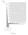
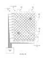
- FIG. 3Aillustrates a sensor array 300 that is connected to a controller 330 .
- sensor array 300may correspond to sensor array 121 in electronic system 100
- the controller 330may correspond to the processing device 110 .
- the controller 330is capable of measuring both self capacitances of sensor elements (between the sensor element and a reference node such as ground) and mutual capacitances between sensor elements.
- the controller 330may be used in a self-capacitance mode to determine a presence, but not necessarily a location, of a contact or a conductive object in proximity to the touch-sensing surface having a sensor array 300 .
- the controller 330may further be configured to, in response to detecting a presence of a contact using a self capacitance sense method in a search mode, switch to a mutual capacitance sense method to perform a scan in tracking mode of all or a portion of the intersections of sensor elements in the sensor array 300 to resolve the actual location of one or more contacts.
- the sensor array 300 illustrated in FIG. 3Ahas 10 row sensor elements 310 ( 1 )- 310 ( 10 ) and 8 column sensor elements 320 ( 1 )- 320 ( 8 ).
- the controller 330may scan each intersection of a row sensor element and a column sensor element. The controller thus performs 80 sense operations (10 row elements ⁇ 8 column elements) to scan the entire panel. Assuming that each sense operation takes 200 1-1S, a scan of the entire sensor array 300 in mutual capacitance mode would take at least 16 ms.
- the controller 330initially operates in self capacitance mode. Scanning of the entire sensor array 300 in a self-capacitance mode can be accomplished with 18 sense operations (10 rows+8 columns). Assuming a similar time (200 !As) per sense operation, a scan of the entire sensor array 300 would take 3.6 ms. This time can be further reduced if the purpose of the scan is to determine the presence of a contact without regard to the location of the contact. To determine the presence of a touch without regard to location, a set of sensor elements may be scanned, such as a subset including only the row elements or only the column elements. Alternatively, the scanned subset may include only alternate row or column elements, or may include only enough sensor elements such that a contact may be detected reliably.
- a sense channelincludes hardware capable of performing a single capacitance measurement at a given time. Assuming a similar time per sense operation of 200 ⁇ s the duration of such a scan could be reduced to as little as 1.6 ms when the sensors of only the vertical axis 320 ( 1 )- 320 ( 8 ) are measured individually.
- the controller 330 in self capacitance modedetermines that a contact is present at the touch-sensing surface if the measured self capacitance of any of the scanned sensor elements exceeds a threshold.
- the self capacitance scan timecan be decreased even more through the use of parallel sensing.
- a controller 330may include eight capacitive sensing channels operating in parallel, such as those found in the CY8CTMA300E, manufactured by Cypress Semiconductor Corporation of San Jose, Calif. With parallel sensing, capacitance sensing of the entire panel may be accomplished using 10 sense operations, since the column elements may be sensed simultaneously. This reduces the scanning overhead time and allows more time for computation intensive functions such as touch location resolution and finger tracking, and for sleep operations to conserve power.
- the controllerscans the sensor array 300 by performing self capacitance measurements on sensor elements of the sensor array 300 .
- the controller 330scans a set of sensor elements, such as all of the sensor elements or a subset of all the sensor elements in the sensor array 300 .
- the controller 330 operating in self capacitance modemay scan the row sensor elements 310 without scanning the column sensor elements 320 .
- the controllermay scan the column sensor elements 320 without scanning the row sensor elements 310 .
- the controllermay alternately scan the column sensor elements 320 and the row sensor elements 310 .
- the self capacitance scanmay be run repeatedly in a loop much faster than scanning the entire panel. Assuming similar measurement times for a single self capacitance measurement as for a mutual capacitance measurement, and that the computation time for the threshold analysis is simpler than the calculation of contact locations, the maximum first-touch delay may be significantly reduced. In one embodiment, the maximum first-touch response delay is changed from approximately twice the duration of a full mutual capacitance scan to the duration of a full scan plus the duration of one self-capacitance measurement. In one embodiment, when a contact is detected at the touch sensing surface, the controller 330 switches to operation in tracking mode, scanning the sensor elements of sensor array 300 using the mutual capacitance method to resolve the locations of the contacts.
- one or more contacts at the touch sensing surfacemay be located during a tracking mode resolve scan using a combination of data provided by a preceding self capacitance scan. For example, determining the locations of the one or more contacts while in tracking mode may include using information from a search scan performed using a self capacitance sense method to identify possible contact locations, then performing a resolve scan while in tracking mode to identify which of the possible contact locations may be actual contact locations.
- the resolve scanincludes a mutual capacitance scan of each of the possible contact locations.
- a complete scan of the sensor array 300 using a self capacitance methodwould include N+M self capacitance measurements for a matrix of N rows ⁇ M columns of sensor elements.
- a maximum of C 2 possible contact locationsmay be detected using a self capacitance scan.
- the possible contact locationscan be resolved to the C actual contact locations using a resolve scan.
- the resolve scanincludes a mutual capacitance measurement of each pair of sensor elements having intersections at all of the possible contact locations 351 - 354 .
- performing the tracking mode scans according to this methodcan significantly reduce the mutual capacitance scan times. For example, for a sensor array having 100 row sensor elements and 100 column sensor elements, five simultaneous contacts can be resolved using a maximum of 225 capacitance measurements, rather than the 10,000 capacitance measurements that may be used if every row and column intersection is measured using a mutual capacitance method.
- Sensor array 300illustrated in FIG. 3B , includes horizontal sensing elements 310 ( 1 )- 310 ( 10 ) and vertical sensing elements 320 ( 1 )- 320 ( 8 ).
- the touch sensing systemperforms an initial search scan of the sensor array 300 in self capacitance mode by taking measurements of each sensing element in a sequence.
- the search scanmay measure the capacitance at each of the sensing elements 310 ( 1 )- 310 ( 10 ) in a sequence, and then measure the capacitance at each of the sensing elements 320 ( 1 )- 320 ( 8 ) in a sequence.
- the search scanmay measure two or more of the sensing elements in parallel.
- the result of such a scanmay be a histogram 360 for the horizontal (X) axis and a similar histogram 340 for the vertical (Y) axis.
- the X axis histogram 360represents the capacitances measured at the vertical sensor elements 320 ( 1 )- 320 ( 8 ). Since contacts at the touch sensing surface affect these measured capacitances, the locations of such contacts along the X axis may be represented as peaks in the X axis histogram. For example, if two contacts 353 and 354 are applied to the touch sensing surface, the locations along the X axis of contact 353 and contact 354 are represented as peaks 361 and 362 , respectively, in histogram 360 . Similarly, the Y axis histogram 340 represents the capacitances measured at the horizontal sensor elements 310 ( 1 )- 310 ( 10 ). Thus, the locations of contacts 353 and 354 along the Y axis are represented as peaks 342 and 341 , respectively, in the Y axis histogram 340 .
- the systemmay determine the location of the single contact based on the X and Y search scan histograms, since the peak of each histogram indicates the row and column locations of the finger contact.
- the histogramsmay indicate a number of possible contact locations. For example, when the actual contacts 353 and 354 are applied to the touch sensing surface, the resulting peaks 361 , 362 , 341 , and 342 indicate additional possible touch locations 351 and 352 .
- the two contactsare at locations 351 and 352 , or whether the two contacts are at locations 353 and 354 , identical histograms may result.
- the number of possible contact locationsalso increases.
- the resulting histogramsmay indicate up to N 2 possible contact locations.
- the systemmay change to mutual capacitance sensing and perform an additional resolve scan.
- the systemmay perform a resolve scan of the intersections of horizontal and vertical sensor elements corresponding to one or more of the peaks, such as peaks 361 , 362 , 341 , or 342 , detected during the initial scan.
- the systembegins by performing a search mode scan of all row and column sensing elements sequentially or in parallel, using a self capacitance measurement technique. The system then performs a resolve scan measuring mutual capacitances when possible contact locations are detected. In one embodiment, if multiple peaks, such as peaks 361 and 362 , are detected in the X axis histogram and multiple peaks, such as peaks 341 and 342 , are detected in the Y axis histogram, the system performs the resolve scan.
- performing the resolve scanmay include performing a mutual capacitance measurement of all intersections of X and Y sensor elements where a possible touch may exist as indicated by the histogram peaks acquired from a search scan. Note that it is necessary to scan all such possible locations, because the histograms 340 and 360 could be generated by touch location combinations of a) 351 and 352 , b) 353 and 354 , c) 351 , 352 , and 353 , d) 351 , 352 , and 354 , e) 352 , 353 , and 354 , f) 351 , 353 , and 354 , and 351 , 352 , 353 , and 354 .
- the systemthus conducts a first mutual capacitance measurement of the intersection between sensor elements 320 ( 2 ) and 310 ( 3 ), a second mutual capacitance measurement of the intersection between sensor elements 320 ( 2 ) and 310 ( 8 ), a third mutual scan measurement of the intersection between sensor elements 320 ( 7 ) and 310 ( 3 ), and a fourth mutual scan measurement of the intersection between sensor elements 320 ( 7 ) and 310 ( 8 ).
- an ADC value measured from the first mutual capacitance measurement of an identified intersectione.g. 320 ( 2 ) and 310 ( 3 )
- when compared to a baseline value for that same intersectionwill be lower than a baseline value for that intersection.
- the ADC values measured from each of the resolve scansmay be compared to each other to determine the location of the actual contact.
- the resolve scan ADC valuesmay be compared with the ADC values measured from a baseline measurement of an intersection, taken when no contact is present at the intersection. The system can then determine the actual contact locations based on this comparison.
- the sensor arraymay be a capacitive sensor having enhanced sensitivity to changes in mutual capacitance between sensor elements, rather than to changes in self capacitance of each sensor element.
- an electronic systemsuch as system 100 may include a touch sensor array having N rows and M columns.
- Such an electronic systemmay include processing logic, such as processing logic 102 that is configured to detect multiple contacts at a touch sensing surface.
- a usermay place two fingers of the same hand to the touch sensing surface, and the system may detect the locations of the two fingers.
- the fingersmay contact the sensing surface at locations 353 and 354 , resulting in peaks 361 and 362 in the X axis histogram 360 and peaks 342 and 341 in the Y axis histogram 340 .
- the systemmay assess the data from the histograms to eliminate special cases where the resolve scan may not be needed. For example, if two contacts exist that are aligned in the X or Y directions, the resolve scan may not be performed. In this case, the two contacts result in only two possible contact locations because one of the histograms detects only one peak for both contacts. In response to detecting this case, the system may determine both of the possible contact locations to be actual contact locations.
- a controller 330can determine the possible locations of one or more contacts at the touch sensing surface when operating in the tracking mode.
- the controller 330may be reconfigured to revert to a search mode where it may look for the presence of contacts using a self capacitance mode.
- the delay between detecting that no contacts are present at the touch-sensing surface and switching to self capacitance search modemay be configurable.
- the switch from mutual capacitance tracking mode to self capacitance search modeoccurs immediately following a complete tracking mode scan of the sensor array 300 during which no contacts are detected.
- the axis with fewer sensor elementsis scanned during a search scan using the self capacitance method to reduce the time for completing the scan.
- controller 330may scan the eight column sensor elements 320 rather than the ten row sensor elements 310 .
- the self capacitance measurements for each of the sensor elements being scannedmay be taken simultaneously.
- sensor elements in the sensor array 300may be grouped together to reduce power consumption.
- the column sensor elements 320may be connected together and sensed using a single sense channel.
- power consumption during a search scanmay be reduced to that of a single sense channel. This method may be used to reduce overall power consumption when determining the presence of a contact at the touch-sensing surface in the search mode.
- the row elements 310when sensing the column elements 320 for self capacitance, the row elements 310 may be driven with a common shield drive signal. In this case, the signal to noise ratio may be improved because the charge may not be coupled through all the intersections in each column to rows that each column intersects. Thus, the change in coupled charge attributable to a contact at the touch-sensing surface may be increased.
- the sensor elements 310 and 320 of the sensor array 300may be divided into a number of zones.
- the sensor array 300may be divided into two zones, each including a subset of five row sensor elements.
- the presence of a contact at the touch-sensing surfacecan then be determined by a pair of sense operations, with one sense operation for each zone.
- the controller 330can be reconfigured to tracking mode to scan either the entire sensor array 300 to determine the locations of any contacts at the touch-sensing surface, or just that zone wherein a one or more contacts was detected.
- the zonesmay be interleaved so that the sensor elements of one zone are interleaved with the sensor elements of another zone.
- a first zonemay include the, odd numbered rows 310 ( 1 ), 310 ( 3 ), 310 ( 5 ), 310 ( 7 ), and 310 ( 9 ) of sensor array 300
- a second zonemay include the even numbered rows 310 ( 2 ), 310 ( 4 ), 310 ( 6 ), 310 ( 8 ), and 310 ( 10 ).
- the rowsare spaced sufficiently close together, a high probability exists that a finger or other object contacting the touch-sensing surface can be detected by a search scan of at least one of the zones.
- the search scanmay be performed repeatedly on a single zone, or alternatively, may alternate between two or more zones.
- the sensor array 300 matrixmay be reversed. For example, row elements that were previously driven with a shield signal can be configured to measure for self capacitance while the column elements previously configured to measure self capacitance are driven with a shield signal.
- FIG. 4illustrates the sensor array 300 connected with a controller 330 , which are also illustrated in FIGS. 3A and 3B .
- FIG. 4also illustrates a contact 340 at the intersection of row sensor element 310 ( 7 ) and column sensor element 320 ( 4 ).
- the controller 330performs a search scan to identify an initial location of the contact 340 , identifies a subset of active sensor elements based on the initial location of the contact 340 , then enters a tracking mode where the controller 330 scans the subset of active sensor elements using a mutual capacitance measurement method to track the movement of contact 340 .
- the controllermay measure intersections associated with a subset of active sensor elements including row sensor elements 310 ( 6 ), 310 ( 7 ), and 310 ( 8 ) and column sensor elements 320 ( 3 ), 320 ( 4 ), and 320 ( 5 ).
- a controller 330may detect the presence of the contact 340 using a self capacitance measurement method while in a search mode, as previously described. In response to determining the presence of the contact 340 , the controller 330 may transition to a tracking mode. The controller 330 may then identify a subset of sensor intersections wherein mutual capacitance should be measured based on the initial location of the contact 340 . In one embodiment, the initial row or column location of the contact 340 may be determined from a self capacitance scan performed while in search mode.
- the controller 330may identify an active subset of sensor elements where each of the sensor elements in the subset is adjacent to a sensor element over which the initial location of contact 340 lies. For example, each of the sensor elements 310 ( 6 ), 310 ( 7 ), 310 ( 8 ), 320 ( 3 ), 320 ( 4 ), and 320 ( 5 ) in the subset of sensor elements illustrated in FIG. 4 lies under contact 340 or is adjacent to a sensor element lying under contact 340 .
- the active subset of sensor elementsmay be chosen such that each sensor element in the active subset intersects another sensor element within a threshold radius of a centroid location calculated for the initial location of contact 340 .
- the active subsetis determined according to some other criteria indicating that certain sensor elements are likely to be affected by future movement of the contact 340 .
- the controller 330reduces the scan time for determining locations of contacts at the touch sensing surface by performing mutual capacitance measurements of intersections between the active sensor elements in the active subset while refraining from measuring intersections between inactive sensor elements. For example, a tracking scan may be performed using a mutual capacitance method that measures each of the intersections between row and column sensor elements in the active subset.
- measurementsare taken at all intersections of sensor elements in sensor array 300 , and used as a basis for calculating a centroid location of the contact 340 .
- sensor array 300includes 18 sensor elements: ten row sensor elements 310 and eight column sensor elements 320 .
- a mutual capacitance scan of every intersection of sensor elements in the sensor array 300would include 8 ⁇ 10, or 80, mutual capacitance measurements.
- the speed of the resolve scancan be increased by avoiding the measurement of intersections of the twelve inactive sensor elements. This can also reduce power consumption by the scanning operation. Assuming that six of the sensor elements, 310 ( 6 ), 310 ( 7 ), 310 ( 8 ), 320 ( 3 ), 320 ( 4 ), and 320 ( 5 ), of sensor array 300 are in the active subset, the mutual capacitance scan includes 9 intersections. This takes significantly less time than the full scan of all 80 intersections of the sensor elements.
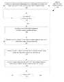
- FIG. 5is a flow diagram illustrating a process for detecting and locating at least one contact at a touch-sensing surface, according to an embodiment.
- Contact detection and location process 500may be performed by a controller such as controller 330 illustrated in FIGS. 3A , 3 B, and 4 .
- the contact detection and location process 500begins at block 502 .
- the controller 330performs a search scan of a first set of sensor elements of a touch-sensing surface to determine a presence of at least one contact that the touch sensing surface.
- the scan of block 502is performed while the controller 330 is operating in a search mode.
- the controller 330may perform a search scan of sensor array 300 , as illustrated in FIG. 4 .
- the search scanmay include self capacitance measurements of a set of sensor elements, which may include all or a subset of the sensor elements of sensor array 300 .
- each of the sensor elements in a scanned subsetmay be a row sensor element 310 .
- each of the sensor elements in the scanned subsetmay be a column sensor element 320 .
- the process 500continues at block 504 .
- the controllerdetermines whether a contact at the touch sensing surface was detected by the scan performed at block 502 . If no contact was detected by the scan of block 502 , the process 500 continues back to block 502 , where the search scan is repeated. Thus, blocks 502 and 504 may be repeated while the controller 330 is operating in search mode until a contact is detected. If at least one contact is detected by the scan of block 502 , the process continues at block 506 .
- the controller 330performs a tracking scan of a second set of sensor elements of the touch-sensing surface.
- the controllerperforms the tracking scan while operating in a tracking mode.
- the tracking scanmay include a mutual capacitance scan for each intersection of a row element 310 and a column element 320 of sensor array 300 .
- the tracking scanincludes identifying and scanning a subset of active sensor elements based on a last known location of the contact. For example, a subset of six active sensor elements 310 ( 6 ), 310 ( 7 ), 310 ( 8 ), 320 ( 3 ), 320 ( 4 ), and 320 ( 5 ) may be included in an active subset for a contact at location 340 .
- the tracking scanmay include a mutual capacitance resolve scan of all intersections of the sensor elements in the active subset to identify the actual contact locations from among a set of possible contact locations determined from the search scan. From block 506 , the process 500 continues at block 508 .
- the controller 330determines whether the contact is no longer present from the touch-sensing surface. If the contact is still present at the touch-sensing surface and has not been lost, the process 500 continues back to block 506 , where the tracking scan is repeated. Thus, the tracking scan may be repeated to continuously track the location of the one or more contacts until the contact is lost. If, at block 508 , the contact is lost, the process 500 continues back to block 502 , where the controller 330 transitions back to search mode.
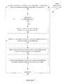
- FIG. 6is a flow diagram illustrating a process for detecting and locating at least one contact at a touch-sensing surface, according to an embodiment.
- Contact detection and location process 600may be performed by a controller such as controller 330 illustrated in FIGS. 3A , 3 B, and 4 .
- the contact detection and location process 600begins at block 602 .
- the controller 330performs a search scan of a zone of a touch-sensing surface to determine a presence of at least one contact that the touch sensing surface.
- the scan of block 602is performed while the controller 330 is operating in a search mode. From block 602 , the process 600 continues at block 604 .
- the controllerdetermines whether a contact at the touch sensing surface was detected by the scan performed at block 602 . If no contact was detected by the scan of block 602 , the process 600 continues back to block 602 , where the search scan is repeated on the next zone. Thus, blocks 602 and 604 may be repeated to scan each zone in sequence while the controller 330 is operating in search mode until a contact is detected. For example, if the sensor array 300 is divided into two zones, the controller 330 may alternately scan the first zone and the second zone. In one embodiment, the each zone includes sensor elements that are contiguous. Alternatively, each zone may include sensor elements that are interleaved with sensor elements of one or more other zones. If at least one contact is detected by the scan of block 602 , the process continues at block 606 .
- the controller 330performs a tracking scan of a second subset of sensor elements of the touch-sensing surface. In one embodiment, the controller performs the tracking scan while operating in a tracking mode. In one embodiment, the tracking scan according to block 606 may be similar to the tracking scan according to block 506 . From block 606 , the process 600 continues at block 608 .
- the controller 330determines whether a contact is present on the touch-sensing surface. If a contact is still present at the touch-sensing surface and has not been lost, the process 600 continues back to block 606 , where the tracking scan is repeated. Thus, the tracking scan may be repeated to continuously track the location of the one or more contacts until contact is lost. If, at block 608 , contact is lost, the process 600 continues back to block 602 , where the controller 330 transitions back to search mode.
- FIG. 7is a flow diagram illustrating a process for detecting and locating at least one contact at a touch-sensing surface, according to an embodiment.
- Contact detection and location process 700may be performed by a controller such as controller 330 illustrated in FIGS. 3A , 3 B, and 4 .
- Contact detection and location process 700begins at block 702 , where the controller 330 operates in search mode, performing a search scan of alternate rows to determine a presence of at least one contact at the touch-sensing surface.
- the search scanis performed by scanning all the rows, all the columns, alternating columns, or another subset of the sensor elements in the sensor array 300 .
- the controller 330scans a minimum number of sensor elements for a contact to be reliably detected. From block 702 , the process 700 continues at block 704 .
- the controller 330determines whether at least one contact is detected at the touch-sensing surface. If, at block 704 , at least one contact is not present at the touch-sensing surface, the process 700 continues back to block 702 , where the search scan is repeated. In one embodiment, if block 702 is entered from block 704 , the operation in block 704 may also be modified to sense elements other than those measured in the previous pass through block 702 . Thus, the search scan may be repeated until a contact is detected. If, at block 704 , the contact is detected at the touch-sensing surface, the process 700 continues at block 706
- the controller 330performs a scan of alternate columns to identify an active column element.
- the scanis performed by scanning a different subset of sensor elements, such as all the rows, alternating rows, or all the columns.
- the sensor elements scanned at block 706may be orthogonal or complementary to the subset of sensor elements scanned at block 702 . For example, if column elements are scanned at block 702 , then row elements may be scanned at block 706 . From block 706 , the process 700 continues at block 708 .
- the controller 330identifies an active subset of row sensor elements based on the row at which the contact was last detected. For example, the row at which the contact was last detected may have been scanned in accordance with block 702 or 706 . Based on the last known row location of the contact, the controller 330 may determine a subset of active sensor elements. In one embodiment, sensor elements adjacent to the row at which the contact was last detected are selected as active sensor elements. Alternatively, the active sensor elements may be sensor elements that intersect other sensor elements within a threshold distance from the last known contact location. In yet another embodiment, the active sensor elements are the sensor elements most likely to be affected by future movement of the contact. From block 708 , the process 700 continues at block 710 .
- the controller 330identifies an active subset of column sensor elements based on the column at which the contact was last detected.
- sensor elements adjacent to the column at which the contact was last detectedare selected as active sensor elements.
- the active sensor elementsmay be sensor elements that intersect other sensor elements within a threshold distance from the last known contact location.
- the active sensor elementsare the sensor elements most likely to be affected by future movement of the contact. From block 710 , the process 700 continues at block 712 .
- the controller 330scans the subset of active sensor elements to determine an updated location of the contact.
- the scanis a mutual capacitance scan of each intersection between sensor elements in the active subset of sensor elements. From block 712 , the process 700 continues at block 716 .
- the controllerdetermines whether a contact is still present at the touch-sensing surface. If a contact is still present at the touch-sensing surface, the process 700 continues back to block 708 , such that the controller 330 remains in tracking mode. If, at block 716 , contact is lost, the process 700 continues back to block 712 , such that the controller 330 transitions back to search mode.
- each of a number of contacts at the touch-sensing surfacemay be associated with an active subset of row and column elements, which may be scanned to track the location of the contact.
- Embodiments of the present inventioninclude various operations. These operations may be performed by hardware components, software, firmware, or a combination thereof.
- the term “coupled to”may mean coupled directly or indirectly through one or more intervening components. Any of the signals provided over various buses described herein may be time multiplexed with other signals and provided over one or more common buses. Additionally, the interconnection between circuit components or blocks may be shown as buses or as single signal lines. Each of the buses may alternatively be one or more single signal lines and each of the single signal lines may alternatively be buses.
- Certain embodimentsmay be implemented as a computer program product that may include instructions stored on a computer-readable medium. These instructions may be used to program a general-purpose or special-purpose processor to perform the described operations.
- a computer-readable mediumincludes any mechanism for storing or transmitting information in a form (e.g., software, processing application) readable by a machine (e.g., a computer).
- the computer-readable storage mediummay include, but is not limited to, magnetic storage medium (e.g., floppy diskette); optical storage medium (e.g., CD-ROM); magneto-optical storage medium; read-only memory (ROM); random-access memory (RAM); erasable programmable memory (e.g., EPROM and EEPROM); flash memory, or another type of medium suitable for storing electronic instructions.
- magnetic storage mediume.g., floppy diskette
- optical storage mediume.g., CD-ROM
- magneto-optical storage mediume.g., magneto-optical storage medium
- ROMread-only memory
- RAMrandom-access memory
- EPROM and EEPROMerasable programmable memory
- flash memoryor another type of medium suitable for storing electronic instructions.
- some embodimentsmay be practiced in distributed computing environments where the computer-readable medium is stored on and/or executed by more than one computer system.
- the information transferred between computer systemsmay either be pulled or pushed across the transmission medium connecting the computer systems.
Landscapes
- Engineering & Computer Science (AREA)
- Theoretical Computer Science (AREA)
- General Engineering & Computer Science (AREA)
- Physics & Mathematics (AREA)
- General Physics & Mathematics (AREA)
- Human Computer Interaction (AREA)
- Position Input By Displaying (AREA)
- Measurement Of Length, Angles, Or The Like Using Electric Or Magnetic Means (AREA)
Abstract
Description
Claims (18)
Priority Applications (1)
| Application Number | Priority Date | Filing Date | Title |
|---|---|---|---|
| US13/950,672US9007342B2 (en) | 2009-07-28 | 2013-07-25 | Dynamic mode switching for fast touch response |
Applications Claiming Priority (3)
| Application Number | Priority Date | Filing Date | Title |
|---|---|---|---|
| US22923609P | 2009-07-28 | 2009-07-28 | |
| US12/844,798US9069405B2 (en) | 2009-07-28 | 2010-07-27 | Dynamic mode switching for fast touch response |
| US13/950,672US9007342B2 (en) | 2009-07-28 | 2013-07-25 | Dynamic mode switching for fast touch response |
Related Parent Applications (1)
| Application Number | Title | Priority Date | Filing Date |
|---|---|---|---|
| US12/844,798ContinuationUS9069405B2 (en) | 2009-07-28 | 2010-07-27 | Dynamic mode switching for fast touch response |
Publications (2)
| Publication Number | Publication Date |
|---|---|
| US20130307823A1 US20130307823A1 (en) | 2013-11-21 |
| US9007342B2true US9007342B2 (en) | 2015-04-14 |
Family
ID=43526533
Family Applications (2)
| Application Number | Title | Priority Date | Filing Date |
|---|---|---|---|
| US12/844,798Active2031-01-17US9069405B2 (en) | 2009-07-28 | 2010-07-27 | Dynamic mode switching for fast touch response |
| US13/950,672ActiveUS9007342B2 (en) | 2009-07-28 | 2013-07-25 | Dynamic mode switching for fast touch response |
Family Applications Before (1)
| Application Number | Title | Priority Date | Filing Date |
|---|---|---|---|
| US12/844,798Active2031-01-17US9069405B2 (en) | 2009-07-28 | 2010-07-27 | Dynamic mode switching for fast touch response |
Country Status (6)
| Country | Link |
|---|---|
| US (2) | US9069405B2 (en) |
| EP (1) | EP2460064A4 (en) |
| KR (1) | KR20120085737A (en) |
| CN (1) | CN102576278B (en) |
| BR (1) | BR112012001958A2 (en) |
| WO (1) | WO2011014580A1 (en) |
Cited By (5)
| Publication number | Priority date | Publication date | Assignee | Title |
|---|---|---|---|---|
| US20140267146A1 (en)* | 2013-03-15 | 2014-09-18 | Novatek Microelectronics Corp. | Touching apparatus and touching detecting method thereof |
| US20140340351A1 (en)* | 2013-03-15 | 2014-11-20 | Clifton Forlines | Fast multi-touch noise reduction |
| US20160306466A1 (en)* | 2015-04-17 | 2016-10-20 | Japan Display Inc. | Touch control method, touch control device and display device having touch detection function |
| US10394368B2 (en) | 2016-05-31 | 2019-08-27 | Microsoft Technology Licensing, Llc | Touch-sensitive display device |
| US20220374126A1 (en)* | 2020-06-03 | 2022-11-24 | Beijing Boe Display Technology Co., Ltd. | Touch panel driving method and apparatus, and touch display device |
Families Citing this family (220)
| Publication number | Priority date | Publication date | Assignee | Title |
|---|---|---|---|---|
| US8144125B2 (en) | 2006-03-30 | 2012-03-27 | Cypress Semiconductor Corporation | Apparatus and method for reducing average scan rate to detect a conductive object on a sensing device |
| US8040142B1 (en) | 2006-03-31 | 2011-10-18 | Cypress Semiconductor Corporation | Touch detection techniques for capacitive touch sense systems |
| US8547114B2 (en) | 2006-11-14 | 2013-10-01 | Cypress Semiconductor Corporation | Capacitance to code converter with sigma-delta modulator |
| US8144126B2 (en) | 2007-05-07 | 2012-03-27 | Cypress Semiconductor Corporation | Reducing sleep current in a capacitance sensing system |
| US9500686B1 (en) | 2007-06-29 | 2016-11-22 | Cypress Semiconductor Corporation | Capacitance measurement system and methods |
| WO2009006557A1 (en)* | 2007-07-03 | 2009-01-08 | Cypress Semiconductor Corporation | Method for improving scan time and sensitivity in touch sensitive user interface device |
| US8089289B1 (en) | 2007-07-03 | 2012-01-03 | Cypress Semiconductor Corporation | Capacitive field sensor with sigma-delta modulator |
| US8570053B1 (en) | 2007-07-03 | 2013-10-29 | Cypress Semiconductor Corporation | Capacitive field sensor with sigma-delta modulator |
| US20090174676A1 (en) | 2008-01-04 | 2009-07-09 | Apple Inc. | Motion component dominance factors for motion locking of touch sensor data |
| US8525798B2 (en) | 2008-01-28 | 2013-09-03 | Cypress Semiconductor Corporation | Touch sensing |
| US8319505B1 (en) | 2008-10-24 | 2012-11-27 | Cypress Semiconductor Corporation | Methods and circuits for measuring mutual and self capacitance |
| JPWO2009107415A1 (en)* | 2008-02-27 | 2011-06-30 | セイコーインスツル株式会社 | Proximity detection device and proximity detection method |
| US8358142B2 (en)* | 2008-02-27 | 2013-01-22 | Cypress Semiconductor Corporation | Methods and circuits for measuring mutual and self capacitance |
| US20160209963A1 (en)* | 2008-03-19 | 2016-07-21 | Egalax_Empia Technology Inc. | Touch processor and method |
| US8321174B1 (en) | 2008-09-26 | 2012-11-27 | Cypress Semiconductor Corporation | System and method to measure capacitance of capacitive sensor array |
| US8487639B1 (en) | 2008-11-21 | 2013-07-16 | Cypress Semiconductor Corporation | Receive demodulator for capacitive sensing |
| US8922521B2 (en) | 2009-02-02 | 2014-12-30 | Apple Inc. | Switching circuitry for touch sensitive display |
| US8866500B2 (en) | 2009-03-26 | 2014-10-21 | Cypress Semiconductor Corporation | Multi-functional capacitance sensing circuit with a current conveyor |
| US8593410B2 (en) | 2009-04-10 | 2013-11-26 | Apple Inc. | Touch sensor panel design |
| US8355887B1 (en) | 2009-04-24 | 2013-01-15 | Cypress Semiconductor Corporation | Proximity based gesturing devices, systems and methods |
| US8957874B2 (en) | 2009-06-29 | 2015-02-17 | Apple Inc. | Touch sensor panel design |
| US9323398B2 (en) | 2009-07-10 | 2016-04-26 | Apple Inc. | Touch and hover sensing |
| US9069405B2 (en) | 2009-07-28 | 2015-06-30 | Cypress Semiconductor Corporation | Dynamic mode switching for fast touch response |
| US8723827B2 (en)* | 2009-07-28 | 2014-05-13 | Cypress Semiconductor Corporation | Predictive touch surface scanning |
| US8723825B2 (en) | 2009-07-28 | 2014-05-13 | Cypress Semiconductor Corporation | Predictive touch surface scanning |
| KR101851264B1 (en)* | 2010-01-06 | 2018-04-24 | 주식회사 셀루온 | System and Method for a Virtual Multi-touch Mouse and Stylus Apparatus |
| CN101840293B (en)* | 2010-01-21 | 2012-03-21 | 宸鸿科技(厦门)有限公司 | Scanning method for projected capacitive touch panels |
| TWI434207B (en)* | 2010-03-25 | 2014-04-11 | Novatek Microelectronics Corp | Touch sensing system, electronic touch apparatus, and touch sensing method |
| CN101840297B (en)* | 2010-04-07 | 2012-09-05 | 敦泰科技(深圳)有限公司 | Touch detection method and detection circuit of capacitance-type touch screen |
| US9766733B2 (en)* | 2010-04-16 | 2017-09-19 | Microchip Technology Germany Gmbh | TFT display, OLED interface and method for detecting the spatial position of extremities in a spatial region located in front of the display |
| US8624870B2 (en)* | 2010-04-22 | 2014-01-07 | Maxim Integrated Products, Inc. | System for and method of transferring charge to convert capacitance to voltage for touchscreen controllers |
| US8493356B2 (en) | 2010-04-22 | 2013-07-23 | Maxim Integrated Products, Inc. | Noise cancellation technique for capacitive touchscreen controller using differential sensing |
| US9391607B2 (en) | 2010-04-22 | 2016-07-12 | Qualcomm Technologies, Inc. | Use of random sampling technique to reduce finger-coupled noise |
| US9652088B2 (en) | 2010-07-30 | 2017-05-16 | Apple Inc. | Fabrication of touch sensor panel using laser ablation |
| TWI436244B (en)* | 2010-08-13 | 2014-05-01 | Raydium Semiconductor Corp | Touch input device and scanning method threrof |
| CN102576276B (en)* | 2010-08-23 | 2017-05-10 | 谱瑞科技股份有限公司 | Capacitive Scan Proximity Detection |
| US8729913B2 (en)* | 2010-08-24 | 2014-05-20 | Cypress Semiconductor Corporation | Capacitance sensing systems, circuits and methods that include current conveyor based oscillators |
| US9851829B2 (en) | 2010-08-27 | 2017-12-26 | Apple Inc. | Signal processing for touch and hover sensing display device |
| JP2012113485A (en)* | 2010-11-24 | 2012-06-14 | Sony Corp | Touch panel device and touch panel detection method |
| US20130285966A1 (en)* | 2010-12-28 | 2013-10-31 | Sharp Kabushiki Kaisha | Display apparatus |
| US9965094B2 (en) | 2011-01-24 | 2018-05-08 | Microsoft Technology Licensing, Llc | Contact geometry tests |
| US8988087B2 (en) | 2011-01-24 | 2015-03-24 | Microsoft Technology Licensing, Llc | Touchscreen testing |
| US8982061B2 (en) | 2011-02-12 | 2015-03-17 | Microsoft Technology Licensing, Llc | Angular contact geometry |
| US9542092B2 (en) | 2011-02-12 | 2017-01-10 | Microsoft Technology Licensing, Llc | Prediction-based touch contact tracking |
| US8773377B2 (en) | 2011-03-04 | 2014-07-08 | Microsoft Corporation | Multi-pass touch contact tracking |
| CN102722297B (en)* | 2011-03-30 | 2016-01-13 | 中兴通讯股份有限公司 | A kind of touch panel device and the method realized close to induction thereof |
| US9268441B2 (en)* | 2011-04-05 | 2016-02-23 | Parade Technologies, Ltd. | Active integrator for a capacitive sense array |
| US8847911B2 (en)* | 2011-04-05 | 2014-09-30 | Cypress Semiconductor Corporation | Circuit to provide signal to sense array |
| TWI469004B (en)* | 2011-04-08 | 2015-01-11 | Raydium Semiconductor Corp | Driving and sensing method for touch input device, and module using the same |
| DE102011017383A1 (en)* | 2011-04-18 | 2012-10-18 | Ident Technology Ag | OLED interface |
| US20120261199A1 (en)* | 2011-04-18 | 2012-10-18 | Silicon Integrated Systems Corp. | Hierarchical sensing method |
| US9377905B1 (en)* | 2011-05-31 | 2016-06-28 | Parade Technologies, Ltd. | Multiplexer for a TX/RX capacitance sensing panel |
| US8913019B2 (en) | 2011-07-14 | 2014-12-16 | Microsoft Corporation | Multi-finger detection and component resolution |
| US9285932B1 (en)* | 2011-07-28 | 2016-03-15 | Parade Technologies, Ltd. | Negative touch recovery for mutual capacitance scanning systems |
| CN102902392A (en)* | 2011-07-29 | 2013-01-30 | 矽统科技股份有限公司 | Hierarchical induction method |
| US9378389B2 (en) | 2011-09-09 | 2016-06-28 | Microsoft Technology Licensing, Llc | Shared item account selection |
| CN102999198B (en)* | 2011-09-16 | 2016-03-30 | 宸鸿科技(厦门)有限公司 | Touch panel edge holds detection method and the device of touch |
| US9612265B1 (en)* | 2011-09-23 | 2017-04-04 | Cypress Semiconductor Corporation | Methods and apparatus to detect a conductive object |
| US8903679B2 (en) | 2011-09-23 | 2014-12-02 | Cypress Semiconductor Corporation | Accuracy in a capacitive sense array |
| US9490804B2 (en)* | 2011-09-28 | 2016-11-08 | Cypress Semiconductor Corporation | Capacitance sensing circuits, methods and systems having conductive touch surface |
| US20130082936A1 (en)* | 2011-09-29 | 2013-04-04 | Sharp Kabushiki Kaisha | Sensor array with high linearity |
| US8810544B2 (en)* | 2011-10-13 | 2014-08-19 | Himax Technologies Limited | Touch sensing method and electronic apparatus using the same |
| FR2981765B1 (en)* | 2011-10-20 | 2013-12-27 | Stantum | METHOD FOR ACQUIRING DATA OF A MATRIX TOUCH SENSOR, IN PARTICULAR FOR A TOUCH SCREEN |
| US8797287B2 (en) | 2011-10-28 | 2014-08-05 | Atmel Corporation | Selective scan of touch-sensitive area for passive or active touch or proximity input |
| US20130106711A1 (en)* | 2011-10-31 | 2013-05-02 | Silicon Integrated Systems Corp. | Hierarchical sensing method |
| US9785281B2 (en) | 2011-11-09 | 2017-10-10 | Microsoft Technology Licensing, Llc. | Acoustic touch sensitive testing |
| US9634660B2 (en)* | 2011-12-20 | 2017-04-25 | Atmel Corporation | Touch sensor with reduced anti-touch effects |
| US9965105B2 (en) | 2011-12-28 | 2018-05-08 | Synaptics Incorporated | Systems and methods for detecting low ground mass conditions in sensor devices |
| CN103186298B (en)* | 2011-12-29 | 2016-06-22 | 旭曜科技股份有限公司 | Low standby power consumption driving method and device for capacitive multi-touch |
| US9310943B1 (en)* | 2012-01-17 | 2016-04-12 | Parade Technologies, Ltd. | Multi-stage stylus scanning |
| US8914254B2 (en) | 2012-01-31 | 2014-12-16 | Microsoft Corporation | Latency measurement |
| TW201335818A (en)* | 2012-02-16 | 2013-09-01 | Elan Microelectronics Corp | Scan method for capacitive touch panel |
| KR101898979B1 (en)* | 2012-02-16 | 2018-09-17 | 삼성디스플레이 주식회사 | Method of operating a touch panel, touch panel and display device |
| US8823664B2 (en)* | 2012-02-24 | 2014-09-02 | Cypress Semiconductor Corporation | Close touch detection and tracking |
| CN102662536B (en)* | 2012-03-07 | 2015-12-09 | 旭曜科技股份有限公司 | A switching mode driving method for capacitive multi-touch |
| US9218093B2 (en) | 2012-03-16 | 2015-12-22 | Parade Technologies, Ltd. | Touch sensor driver with selectable charge source |
| US20140267152A1 (en)* | 2013-03-12 | 2014-09-18 | Mircrochip Technology Incorporated | Force Sensing X-Y Touch Sensor |
| US9430107B2 (en)* | 2012-03-30 | 2016-08-30 | Microchip Technology Incorporated | Determining touch locations and forces thereto on a touch and force sensing surface |
| US9207820B2 (en)* | 2012-03-30 | 2015-12-08 | Microchip Technology Incorporated | Method and system for multi-touch decoding |
| TWI463386B (en)* | 2012-04-03 | 2014-12-01 | Elan Microelectronics Corp | A method and an apparatus for improving noise interference of a capacitive touch device |
| US9329723B2 (en) | 2012-04-16 | 2016-05-03 | Apple Inc. | Reconstruction of original touch image from differential touch image |
| KR101307227B1 (en)* | 2012-04-17 | 2013-09-11 | 주식회사 리딩유아이 | Multi-touch sensing device |
| JP2013222387A (en)* | 2012-04-18 | 2013-10-28 | Japan Display Inc | Display device |
| CN104603729B (en) | 2012-04-27 | 2018-02-02 | 阿尔申蒂斯有限责任公司 | Apparatus for determining touch input stimuli |
| US8913021B2 (en)* | 2012-04-30 | 2014-12-16 | Apple Inc. | Capacitance touch near-field—far field switching |
| US9086768B2 (en) | 2012-04-30 | 2015-07-21 | Apple Inc. | Mitigation of parasitic capacitance |
| US9201547B2 (en) | 2012-04-30 | 2015-12-01 | Apple Inc. | Wide dynamic range capacitive sensing |
| US9024643B2 (en)* | 2012-06-28 | 2015-05-05 | Synaptics Incorporated | Systems and methods for determining types of user input |
| US10754477B2 (en) | 2012-06-28 | 2020-08-25 | Texas Instruments Incorporated | Capacitive proximity detection system and method |
| US20140002406A1 (en)* | 2012-06-28 | 2014-01-02 | Texas Instruments Incorporated | Low-Power Capacitive Sensor Monitoring and Method |
| US9182432B2 (en) | 2012-07-18 | 2015-11-10 | Synaptics Incorporated | Capacitance measurement |
| KR20140017255A (en)* | 2012-07-31 | 2014-02-11 | 삼성전자주식회사 | Electric pen input recognition apparatus and method using c-type tsp |
| US9213052B2 (en)* | 2012-08-01 | 2015-12-15 | Parade Technologies, Ltd. | Peak detection schemes for touch position detection |
| US8917253B2 (en) | 2012-08-31 | 2014-12-23 | Blackberry Limited | Method and apparatus pertaining to the interlacing of finger-based and active-stylus-based input detection |
| EP2703966A1 (en)* | 2012-08-31 | 2014-03-05 | BlackBerry Limited | Method and apparatus pertaining to the interlacing of finger-based and active-stylus-based input detection |
| US8816985B1 (en)* | 2012-09-20 | 2014-08-26 | Cypress Semiconductor Corporation | Methods and apparatus to detect a touch pattern |
| US9310924B2 (en) | 2012-09-26 | 2016-04-12 | Atmel Corporation | Increasing the dynamic range of an integrator based mutual-capacitance measurement circuit |
| ITTO20120842A1 (en)* | 2012-09-27 | 2014-03-28 | St Microelectronics Srl | PROCEDURE AND SYSTEM FOR DETECTION DETECTION, RELATED SCREEN EQUIPMENT AND COMPUTER PRODUCT |
| ITTO20120864A1 (en)* | 2012-10-04 | 2014-04-05 | St Microelectronics Srl | PROCEDURE AND SYSTEM FOR RECOGNITION OF FORMS OF THE TOUCH, SCREEN EQUIPMENT AND ITS RELATED PRODUCT |
| US9317147B2 (en) | 2012-10-24 | 2016-04-19 | Microsoft Technology Licensing, Llc. | Input testing tool |
| JP2014102747A (en)* | 2012-11-21 | 2014-06-05 | Panasonic Liquid Crystal Display Co Ltd | Touch panel device and control method of touch panel device |
| CN102968235B (en)* | 2012-11-27 | 2015-12-02 | 深圳市汇顶科技股份有限公司 | The touch detecting method of touch sensor, system and touch control terminal |
| KR102143945B1 (en)* | 2012-11-30 | 2020-08-13 | 엘지디스플레이 주식회사 | Touch sensing system |
| KR101472203B1 (en)* | 2013-03-04 | 2014-12-12 | 주식회사 동부하이텍 | Signal processing circuit of a touch screen |
| US9110552B2 (en)* | 2013-03-11 | 2015-08-18 | Cypress Semiconductor Corporation | Eliminating common mode noise in otuch applications |
| US8810263B1 (en) | 2013-03-12 | 2014-08-19 | Cypress Semiconductor Corporation | Adaptive resolution circuit |
| US8779783B1 (en)* | 2013-03-12 | 2014-07-15 | Cypress Semiconductor Corporation | Mutual capacitance sensing using a self-capacitance sensing device |
| US9035906B2 (en) | 2013-03-13 | 2015-05-19 | Synaptics Incorporated | Proximity sensing |
| US9310457B2 (en) | 2013-03-13 | 2016-04-12 | Synaptics Incorporated | Baseline management for sensing device |
| US9652091B1 (en)* | 2013-03-15 | 2017-05-16 | Amazon Technologies, Inc. | Touch sensitive display utilizing mutual capacitance and self capacitance |
| CN104063096B (en)* | 2013-03-18 | 2017-05-24 | 原相科技股份有限公司 | capacitive touch device |
| JP5884770B2 (en)* | 2013-05-21 | 2016-03-15 | トヨタ自動車株式会社 | Contact detection device |
| CN103294323A (en)* | 2013-06-13 | 2013-09-11 | 敦泰科技有限公司 | Method and device for touch detection and touch screen system |
| US20140375594A1 (en)* | 2013-06-24 | 2014-12-25 | Texas Instruments Incorporated | Touch screen system and method |
| US9612677B2 (en)* | 2013-06-28 | 2017-04-04 | Atmel Corporation | Pseudo driven shield |
| US20150015528A1 (en)* | 2013-07-10 | 2015-01-15 | Synaptics Incorporated | Hybrid capacitive image determination and use |
| US9507472B2 (en) | 2013-07-10 | 2016-11-29 | Synaptics Incorporated | Hybrid capacitive baseline management |
| KR101307228B1 (en) | 2013-07-24 | 2013-09-11 | 주식회사 리딩유아이 | Multi-touch sensing device |
| KR20150014679A (en)* | 2013-07-30 | 2015-02-09 | 삼성전자주식회사 | Display apparatus and control method thereof |
| US9552089B2 (en) | 2013-08-07 | 2017-01-24 | Synaptics Incorporated | Capacitive sensing using a matrix electrode pattern |
| US9886141B2 (en)* | 2013-08-16 | 2018-02-06 | Apple Inc. | Mutual and self capacitance touch measurements in touch panel |
| CN105474154B (en)* | 2013-08-16 | 2019-05-14 | 苹果公司 | Touch Panel Electrode Structure for User Ground Correction |
| JP2015045909A (en)* | 2013-08-27 | 2015-03-12 | 株式会社東海理化電機製作所 | Operation input device |
| US8872526B1 (en)* | 2013-09-10 | 2014-10-28 | Cypress Semiconductor Corporation | Interleaving sense elements of a capacitive-sense array |
| US9495050B1 (en) | 2013-09-10 | 2016-11-15 | Monterey Research, Llc | Sensor pattern with signal-spreading electrodes |
| KR101486493B1 (en)* | 2013-09-25 | 2015-01-27 | 주식회사 애트랩 | Touch sensing apparatus using hybrid capacitance sensing operation and method thereof |
| US9274659B2 (en) | 2013-09-27 | 2016-03-01 | Synaptics Incorporated | Transcapacitive input object sensing |
| US10042489B2 (en)* | 2013-09-30 | 2018-08-07 | Synaptics Incorporated | Matrix sensor for image touch sensing |
| US20150091842A1 (en) | 2013-09-30 | 2015-04-02 | Synaptics Incorporated | Matrix sensor for image touch sensing |
| US9405415B2 (en) | 2013-10-01 | 2016-08-02 | Synaptics Incorporated | Targeted transcapacitance sensing for a matrix sensor |
| US8823399B1 (en)* | 2013-10-07 | 2014-09-02 | Cypress Semiconductor Corporation | Detect and differentiate touches from different size conductive objects on a capacitive button |
| KR20150042366A (en)* | 2013-10-10 | 2015-04-21 | 삼성전자주식회사 | Touch screen sensror integrated circuit, method thereof, and system having the same |
| CN103927042B (en)* | 2013-10-31 | 2017-02-01 | 上海中航光电子有限公司 | Touch point positioning method and device and electronic device |
| US9933879B2 (en) | 2013-11-25 | 2018-04-03 | Apple Inc. | Reconfigurable circuit topology for both self-capacitance and mutual capacitance sensing |
| US9304575B2 (en) | 2013-11-26 | 2016-04-05 | Apple Inc. | Reducing touch sensor panel power consumption |
| KR20160105465A (en) | 2014-01-03 | 2016-09-06 | 쓰리엠 이노베이티브 프로퍼티즈 컴파니 | Capacitive touch systems and methods using differential signal techniques |
| KR102313098B1 (en)* | 2014-02-18 | 2021-10-14 | 케임브리지 터치 테크놀로지스 리미티드 | Dynamic switching of power modes for touch screens using force touch |
| CN103823596A (en)* | 2014-02-19 | 2014-05-28 | 青岛海信电器股份有限公司 | Touch scanning method and device |
| TWI512585B (en)* | 2014-03-07 | 2015-12-11 | Elan Microelectronics Corp | Capacitive touch panel and manufacture method thereof |
| US9753570B2 (en) | 2014-03-14 | 2017-09-05 | Synaptics Incorporated | Combined capacitive sensing |
| US11093093B2 (en) | 2014-03-14 | 2021-08-17 | Synaptics Incorporated | Transcapacitive and absolute capacitive sensing profiles |
| US9582112B2 (en) | 2014-03-21 | 2017-02-28 | Synaptics Incorporated | Low ground mass artifact management |
| US9727181B2 (en) | 2014-03-28 | 2017-08-08 | Synaptics Incorporated | Method and system for low ground mass correction |
| US9939966B2 (en) | 2014-03-28 | 2018-04-10 | Synaptics Incorporated | Low ground mass correction mechanism |
| US9354743B2 (en)* | 2014-04-16 | 2016-05-31 | Microchip Technology Incorporated | Apparatus for improving signal-to-noise performance of projected capacitance touch screens and panels |
| WO2015178920A1 (en) | 2014-05-22 | 2015-11-26 | Onamp Research Llc | Panel bootstrapping architectures for in-cell self-capacitance |
| JP6400944B2 (en)* | 2014-05-26 | 2018-10-03 | シナプティクス・ジャパン合同会社 | Capacitance detection circuit, touch detection circuit, and semiconductor integrated circuit including the same |
| US9151792B1 (en) | 2014-05-29 | 2015-10-06 | Cyress Semiconductor Corporation | High-voltage, high-sensitivity self-capacitance sensing |
| CN104020908B (en)* | 2014-05-30 | 2017-03-01 | 京东方科技集团股份有限公司 | A kind of driving method of In-cell touch panel, device and display device |
| US9703431B2 (en) | 2014-06-03 | 2017-07-11 | Synaptics Incorporated | Noise detection and mitigation for capacitive sensing devices |
| US9753587B2 (en) | 2014-06-05 | 2017-09-05 | Synaptics Incorporated | Driving sensor electrodes for absolute capacitive sensing |
| US9417729B2 (en)* | 2014-06-09 | 2016-08-16 | Atmel Corporation | Charge compensation during touch sensing |
| US10289251B2 (en) | 2014-06-27 | 2019-05-14 | Apple Inc. | Reducing floating ground effects in pixelated self-capacitance touch screens |
| US9703430B2 (en)* | 2014-06-30 | 2017-07-11 | Synaptics Incorporated | Driving sensor electrodes for proximity sensing |
| US10429998B2 (en)* | 2014-07-23 | 2019-10-01 | Cypress Semiconductor Corporation | Generating a baseline compensation signal based on a capacitive circuit |
| US9746974B2 (en) | 2014-08-21 | 2017-08-29 | Cypress Semiconductor Corporation | Providing a baseline capacitance for a capacitance sensing channel |
| KR102417018B1 (en)* | 2014-08-26 | 2022-07-05 | 엘지디스플레이 주식회사 | Apparatus for driving of touch panel |
| US9880655B2 (en) | 2014-09-02 | 2018-01-30 | Apple Inc. | Method of disambiguating water from a finger touch on a touch sensor panel |
| WO2016048269A1 (en) | 2014-09-22 | 2016-03-31 | Onamp Research Llc | Ungrounded user signal compensation for pixelated self-capacitance touch sensor panel |
| CN105760026A (en)* | 2014-09-26 | 2016-07-13 | 义隆电子股份有限公司 | scanning method and device of single-layer capacitive touch panel |
| US9891763B2 (en) | 2014-09-30 | 2018-02-13 | Synaptics Incorporated | Current feedback techniques for capacitive sensing |
| US9857925B2 (en) | 2014-09-30 | 2018-01-02 | Synaptics Incorporated | Combining sensor electrodes in a matrix sensor |
| US9542051B2 (en)* | 2014-10-24 | 2017-01-10 | Microchip Technology Incorporated | Analog elimination of ungrounded conductive objects in capacitive sensing |
| EP3213173A4 (en)* | 2014-10-27 | 2018-06-06 | Apple Inc. | Pixelated self-capacitance water rejection |
| JP6366474B2 (en)* | 2014-11-10 | 2018-08-01 | キヤノン株式会社 | Electronic device, control method therefor, program, and recording medium |
| CN104461198B (en)* | 2014-12-03 | 2017-07-07 | 深圳市华星光电技术有限公司 | A kind of touch base plate and terminal |
| WO2016093127A1 (en)* | 2014-12-08 | 2016-06-16 | シャープ株式会社 | Display device, control method for display device, and control program |
| US9791970B2 (en) | 2014-12-22 | 2017-10-17 | Synaptics Incorporated | Method and system for dual node sensing |
| EP3457263A1 (en) | 2014-12-23 | 2019-03-20 | Cambridge Touch Technologies, Ltd. | Pressure-sensitive touch panel |
| GB2533667B (en) | 2014-12-23 | 2017-07-19 | Cambridge Touch Tech Ltd | Pressure-sensitive touch panel |
| CN104503643B (en)* | 2014-12-25 | 2017-10-10 | 上海天马微电子有限公司 | Touch structure, touch detection method and touch display device |
| US10191597B2 (en)* | 2015-06-30 | 2019-01-29 | Synaptics Incorporated | Modulating a reference voltage to preform capacitive sensing |
| US10795471B2 (en) | 2015-01-05 | 2020-10-06 | Synaptics Incorporated | Modulating a reference voltage to perform capacitive sensing |
| US10795488B2 (en) | 2015-02-02 | 2020-10-06 | Apple Inc. | Flexible self-capacitance and mutual capacitance touch sensing system architecture |
| US10037100B2 (en)* | 2015-03-02 | 2018-07-31 | Apple Inc. | SNR-aware active mode touch scans with electrode reallocation |
| US10488992B2 (en) | 2015-03-10 | 2019-11-26 | Apple Inc. | Multi-chip touch architecture for scalability |
| US9746975B2 (en) | 2015-03-27 | 2017-08-29 | Synaptics Incorporated | Capacitive measurement processing for mode changes |
| US9645633B2 (en) | 2015-03-31 | 2017-05-09 | Synaptics Incorporated | Single receiver superdoze mode |
| US9720541B2 (en) | 2015-06-30 | 2017-08-01 | Synaptics Incorporated | Arrangement of sensor pads and display driver pads for input device |
| US9715304B2 (en) | 2015-06-30 | 2017-07-25 | Synaptics Incorporated | Regular via pattern for sensor-based input device |
| US10261619B2 (en) | 2015-08-31 | 2019-04-16 | Synaptics Incorporated | Estimating force applied by an input object to a touch sensor |
| US10365773B2 (en) | 2015-09-30 | 2019-07-30 | Apple Inc. | Flexible scan plan using coarse mutual capacitance and fully-guarded measurements |
| JP6554013B2 (en)* | 2015-10-14 | 2019-07-31 | キヤノン株式会社 | INPUT DEVICE, METHOD OF CONTROLLING INPUT DEVICE, ELECTRONIC DEVICE PROVIDED WITH INPUT DEVICE, METHOD OF CONTROLLING ELECTRONIC DEVICE, PROGRAM, AND STORAGE MEDIUM |
| GB2544307B (en) | 2015-11-12 | 2018-02-07 | Cambridge Touch Tech Ltd | Processing signals from a touchscreen panel |
| JP6560971B2 (en)* | 2015-12-04 | 2019-08-14 | 株式会社ジャパンディスプレイ | Display device and input device |
| GB2544353B (en) | 2015-12-23 | 2018-02-21 | Cambridge Touch Tech Ltd | Pressure-sensitive touch panel |
| US10282046B2 (en) | 2015-12-23 | 2019-05-07 | Cambridge Touch Technologies Ltd. | Pressure-sensitive touch panel |
| KR101733893B1 (en)* | 2015-12-28 | 2017-05-08 | 한양대학교 산학협력단 | Driving circuit for a touch panel for achieving modes with one sensing circuit and method of sensing touch using the same |
| US10067587B2 (en) | 2015-12-29 | 2018-09-04 | Synaptics Incorporated | Routing conductors in an integrated display device and sensing device |
| GB2547031B (en) | 2016-02-05 | 2019-09-25 | Cambridge Touch Tech Ltd | Touchscreen panel signal processing |
| US10540043B2 (en) | 2016-03-02 | 2020-01-21 | Synaptics Incorporated | Hybrid in-cell sensor topology |
| US10146388B2 (en)* | 2016-03-08 | 2018-12-04 | Synaptics Incorporated | Capacitive sensing in an LED display |
| US10126892B2 (en) | 2016-03-16 | 2018-11-13 | Synaptics Incorporated | Moisture management |
| US10078406B2 (en)* | 2016-03-31 | 2018-09-18 | Synaptics Incorporated | Capacitive side position extrapolation |
| US10061415B2 (en) | 2016-06-30 | 2018-08-28 | Synaptics Incorporated | Input device receiver with delta-sigma modulator |
| US11402950B2 (en)* | 2016-07-29 | 2022-08-02 | Apple Inc. | Methodology and application of acoustic touch detection |
| AU2017208277B2 (en) | 2016-09-06 | 2018-12-20 | Apple Inc. | Back of cover touch sensors |
| US10540044B2 (en)* | 2016-12-14 | 2020-01-21 | Cypress Semiconductor Corporation | Capacitive sensing with multi-pattern scan |
| US10216322B2 (en) | 2017-02-01 | 2019-02-26 | Nxp Usa, Inc. | Capacitive touch sense unit computation power reduction using keypad electrodes crosstalk |
| US11487390B2 (en) | 2017-03-28 | 2022-11-01 | Sony Corporation | Information processing apparatus and control method of information processing apparatus |
| US10642418B2 (en) | 2017-04-20 | 2020-05-05 | Apple Inc. | Finger tracking in wet environment |
| CN107102776A (en)* | 2017-05-24 | 2017-08-29 | 努比亚技术有限公司 | A kind of touch-screen control method, device, mobile terminal and storage medium |
| CN107454950B (en)* | 2017-07-20 | 2021-10-19 | 深圳市汇顶科技股份有限公司 | Method for detecting touch point and touch controller |
| GB2565305A (en) | 2017-08-08 | 2019-02-13 | Cambridge Touch Tech Ltd | Device for processing signals from a pressure-sensing touch panel |
| US11093088B2 (en) | 2017-08-08 | 2021-08-17 | Cambridge Touch Technologies Ltd. | Device for processing signals from a pressure-sensing touch panel |
| KR102771451B1 (en) | 2017-08-15 | 2025-02-25 | 애플 인크. | Self-capacitance and mutual capacitance hybrid touch sensor panel architecture |
| WO2019068020A1 (en)* | 2017-09-29 | 2019-04-04 | Apple Inc. | Touch sensor panel architecture with multiple sensing mode capabilities |
| US10503312B2 (en)* | 2018-01-18 | 2019-12-10 | Elo Touch Solutions, Inc. | Large PCAP screen with multiple touch controller ASICS with interleaved receiver connections |
| CN110095664B (en)* | 2018-01-29 | 2021-05-18 | 华润微集成电路(无锡)有限公司 | High-precision touch detection circuit and high-precision touch detection system |
| CN108617051B (en)* | 2018-05-09 | 2020-04-07 | 新茂国际科技股份有限公司 | Touch sensing and LED control circuit for capacitive touch screen |
| US11079882B2 (en) | 2018-09-28 | 2021-08-03 | Apple Inc. | Diamond based touch sensor panel architectures |
| US10936119B2 (en)* | 2019-03-05 | 2021-03-02 | Stmicroelectronics Asia Pacific Pte Ltd | Self capacitance sensing based on tangent of phase shift of drive signal |
| JP7232098B2 (en)* | 2019-03-27 | 2023-03-02 | 株式会社ジャパンディスプレイ | detector |
| US11157109B1 (en) | 2019-09-06 | 2021-10-26 | Apple Inc. | Touch sensing with water rejection |
| KR102804954B1 (en)* | 2019-12-19 | 2025-05-09 | 주식회사 엘엑스세미콘 | Device and method for touch sensing |
| US11662867B1 (en) | 2020-05-30 | 2023-05-30 | Apple Inc. | Hover detection on a touch sensor panel |
| CN112684938B (en)* | 2020-12-31 | 2021-12-21 | 深圳贝特莱电子科技股份有限公司 | Touch screen scanning data adaptive noise control method and system |
| WO2022157417A1 (en)* | 2021-01-21 | 2022-07-28 | Lumineq Oy | Method for an electroluminescent touch display and an electroluminescent touch display |
| CN117294295A (en)* | 2022-06-17 | 2023-12-26 | 深圳贝特莱电子科技股份有限公司 | Structure and method for improving anti-interference performance of touch key and touch product |
| US11853497B1 (en)* | 2022-12-05 | 2023-12-26 | Lenovo (Singapore) Pte. Ltd. | Power management for input device |
Citations (116)
| Publication number | Priority date | Publication date | Assignee | Title |
|---|---|---|---|---|
| US3660801A (en) | 1971-01-11 | 1972-05-02 | Noma World Wide Inc | One-piece socket for decorative light |
| US3921167A (en) | 1974-06-14 | 1975-11-18 | Ibm | Capacitive circuitboard |
| US4686332A (en) | 1986-06-26 | 1987-08-11 | International Business Machines Corporation | Combined finger touch and stylus detection system for use on the viewing surface of a visual display device |
| US4918262A (en) | 1989-03-14 | 1990-04-17 | Ibm Corporation | Touch sensing display screen signal processing apparatus and method |
| US4935728A (en) | 1985-01-02 | 1990-06-19 | Altra Corporation | Computer control |
| US5239140A (en) | 1991-03-08 | 1993-08-24 | Pioneer Electronic Corporation | Pattern input apparatus |
| US5374787A (en) | 1992-06-08 | 1994-12-20 | Synaptics, Inc. | Object position detector |
| US5386584A (en) | 1990-06-14 | 1995-01-31 | Chips And Technologies, Inc. | Interrupt-generating keyboard scanner using an image RAM |
| US5412387A (en) | 1993-04-06 | 1995-05-02 | Analog Devices, Inc. | Error reduction in switched capacitor digital-to-analog converter systems by balanced sampling |
| US5642134A (en) | 1994-11-17 | 1997-06-24 | Nec Corporation | Integrated tablet device having position detecting function and image display function |
| US5825352A (en) | 1996-01-04 | 1998-10-20 | Logitech, Inc. | Multiple fingers contact sensing method for emulating mouse buttons and mouse operations on a touch sensor pad |
| US5872561A (en)* | 1997-03-31 | 1999-02-16 | Allen-Bradley Company, Llc | Fast scanning switch matrix |
| US5920309A (en) | 1996-01-04 | 1999-07-06 | Logitech, Inc. | Touch sensing method and apparatus |
| US6292173B1 (en) | 1998-09-11 | 2001-09-18 | Stmicroelectronics S.R.L. | Touchpad computer input system and method |
| WO2002003368A1 (en) | 2000-06-30 | 2002-01-10 | Bsquare Corporation | Method and apparatus for touch screen noise immunity improvement |
| US20020015024A1 (en) | 1998-01-26 | 2002-02-07 | University Of Delaware | Method and apparatus for integrating manual input |
| US6396484B1 (en) | 1999-09-29 | 2002-05-28 | Elo Touchsystems, Inc. | Adaptive frequency touchscreen controller using intermediate-frequency signal processing |
| US20030058053A1 (en) | 2001-09-25 | 2003-03-27 | Samsung Electronics Co., Ltd. | Phase locked loop for reducing electromagnetic interference |
| US20030161278A1 (en) | 2002-02-25 | 2003-08-28 | Nec Corporation | Symbol data converting circuit |
| US20030184065A1 (en) | 1992-05-05 | 2003-10-02 | Breed David S. | Rear view mirror monitor |
| US20030209893A1 (en) | 1992-05-05 | 2003-11-13 | Breed David S. | Occupant sensing system |
| US20040039298A1 (en) | 1996-09-04 | 2004-02-26 | Abreu Marcio Marc | Noninvasive measurement of chemical substances |
| US20040047110A1 (en) | 2000-11-17 | 2004-03-11 | Alain Friederich | Variable capacitance voltag-controlllable by use of coulomb barrier phenomenon |
| US20040129478A1 (en) | 1992-05-05 | 2004-07-08 | Breed David S. | Weight measuring systems and methods for vehicles |
| US6762752B2 (en) | 2001-11-29 | 2004-07-13 | N-Trig Ltd. | Dual function input device and method |
| US20040173028A1 (en) | 2001-04-27 | 2004-09-09 | Robert Rix | Electroconductive textile sensor |
| US20040209591A1 (en) | 2003-04-21 | 2004-10-21 | Quorum Systems, Inc. | Reconfigurable baseband filter |
| US20050068044A1 (en) | 2001-10-24 | 2005-03-31 | William Peine | Array sensor electronics |
| US20050129292A1 (en) | 2003-12-11 | 2005-06-16 | Smiths Heimann Biometrics Gmbh; | Method and arrangement for electronic recording of rolled fingerprints |
| US20050134292A1 (en) | 2003-12-23 | 2005-06-23 | Dialog Semiconductor Gmbh | Differential capacitance measurement |
| US20060012580A1 (en) | 2004-07-15 | 2006-01-19 | N-Trig Ltd. | Automatic switching for a dual mode digitizer |
| US20060012581A1 (en) | 2004-07-15 | 2006-01-19 | N-Trig Ltd. | Tracking window for a digitizer system |
| US7019672B2 (en) | 1998-12-24 | 2006-03-28 | Synaptics (Uk) Limited | Position sensor |
| US7036096B1 (en) | 2003-09-08 | 2006-04-25 | Sun Microsystems, Inc. | Estimating capacitances using information including feature sizes extracted from a netlist |
| US20060161871A1 (en) | 2004-07-30 | 2006-07-20 | Apple Computer, Inc. | Proximity detector in handheld device |
| US20060192690A1 (en) | 2002-07-12 | 2006-08-31 | Harald Philipp | Capacitive Keyboard with Non-Locking Reduced Keying Ambiguity |
| US7100430B2 (en) | 1994-12-22 | 2006-09-05 | Kla-Tencor Corporation | Dual stage instrument for scanning a specimen |
| US20060197752A1 (en) | 2005-02-17 | 2006-09-07 | Hurst G S | Multiple-touch sensor |
| US20060219692A1 (en) | 2005-02-25 | 2006-10-05 | Peter Unsworth | Pointer for interactive display system |
| US20060256090A1 (en) | 2005-05-12 | 2006-11-16 | Apple Computer, Inc. | Mechanical overlay |
| US20060273804A1 (en) | 2003-06-20 | 2006-12-07 | Commissariat A L'energie Atomique | Capacitive measuring sensor and associated ,measurement method |
| US20070008299A1 (en) | 2005-07-08 | 2007-01-11 | Harald Philipp | Two-Dimensional Position Sensor |
| US20070046299A1 (en) | 2005-06-03 | 2007-03-01 | Kirk Hargreaves | Methods and systems for detecting a capacitance using sigma-delta measurement techniques |
| US20070121959A1 (en) | 2005-09-30 | 2007-05-31 | Harald Philipp | Headset power management |
| US20070143667A1 (en) | 2002-07-22 | 2007-06-21 | Kenneth Deaton | Display system and method for displaying a multi-dimensional file visualizer and chooser |
| US20070152977A1 (en) | 2005-12-30 | 2007-07-05 | Apple Computer, Inc. | Illuminated touchpad |
| US20070182718A1 (en) | 2003-05-30 | 2007-08-09 | Hans-Peter Schoener | Operator control device |
| US20070188518A1 (en) | 2006-02-10 | 2007-08-16 | Microsoft Corporation | Variable orientation input mode |
| US20070229468A1 (en) | 2006-03-30 | 2007-10-04 | Cypress Semiconductor Corporation | Apparatus and method for reducing average scan rate to detect a conductive object on a sensing device |
| US20070229470A1 (en) | 2006-03-31 | 2007-10-04 | Warren Snyder | Capacitive touch sense device having polygonal shaped sensor elements |
| US20070235231A1 (en) | 2006-03-29 | 2007-10-11 | Tekscan, Inc. | Control circuit for sensor array and related methods |
| US20070273659A1 (en) | 2006-05-26 | 2007-11-29 | Xiaoping Jiang | Multi-function slider in touchpad |
| US20080007533A1 (en) | 2006-07-06 | 2008-01-10 | Apple Computer, Inc., A California Corporation | Capacitance sensing electrode with integrated I/O mechanism |
| US20080024455A1 (en) | 2006-07-25 | 2008-01-31 | Lee Mark R | Technique for increasing the sensitivity of capacitive sensor arrays |
| US20080048997A1 (en)* | 1992-06-08 | 2008-02-28 | Synaptics Incorporated | Object position detector with edge motion feature and gesture recognition |
| US20080062148A1 (en) | 2006-06-09 | 2008-03-13 | Hotelling Steve P | Touch screen liquid crystal display |
| US20080072192A1 (en) | 2006-09-18 | 2008-03-20 | Lenahan Terrence A | Capacitor network reduction |
| US20080079699A1 (en) | 2006-10-03 | 2008-04-03 | Bob Lee Mackey | Unambiguous capacitance sensing using shared inputs |
| US7375535B1 (en) | 2005-09-19 | 2008-05-20 | Cypress Semiconductor Corporation | Scan method and topology for capacitive sensing |
| US20080150906A1 (en)* | 2006-12-22 | 2008-06-26 | Grivna Edward L | Multi-axial touch-sensor device with multi-touch resolution |
| US20080158177A1 (en) | 2007-01-03 | 2008-07-03 | Apple Inc. | Master/slave mode for sensor processing devices |
| US20080158180A1 (en) | 2007-01-03 | 2008-07-03 | Apple Inc. | Scan sequence generator |
| US7406393B2 (en) | 2002-03-05 | 2008-07-29 | Synaptics (Uk) Limited | Position sensor |
| US20080180399A1 (en) | 2007-01-31 | 2008-07-31 | Tung Wan Cheng | Flexible Multi-touch Screen |
| US7428191B1 (en)* | 2006-05-01 | 2008-09-23 | Klein Dennis L | Electronic timepiece with inverted digital display |
| US20080246723A1 (en) | 2007-04-05 | 2008-10-09 | Baumbach Jason G | Integrated button activation sensing and proximity sensing |
| US20080277171A1 (en) | 2007-05-07 | 2008-11-13 | Wright David G | Reducing sleep current in a capacitance sensing system |
| US20080309634A1 (en) | 2007-01-05 | 2008-12-18 | Apple Inc. | Multi-touch skins spanning three dimensions |
| US20080309623A1 (en) | 2007-06-13 | 2008-12-18 | Apple Inc. | Touch screens with transparent conductive material resistors |
| US20090009485A1 (en)* | 2007-03-29 | 2009-01-08 | Bytheway Jared G | Driven shield for capacitive touchpads |
| US20090096757A1 (en)* | 2004-05-06 | 2009-04-16 | Steve Hotelling | Multipoint touchscreen |
| US20090128516A1 (en)* | 2007-11-07 | 2009-05-21 | N-Trig Ltd. | Multi-point detection on a single-point detection digitizer |
| US20090160787A1 (en)* | 2007-12-21 | 2009-06-25 | Apple Inc. | Negative pixel compensation |
| US20090273579A1 (en) | 2008-04-30 | 2009-11-05 | N-Trig Ltd. | Multi-touch detection |
| US20090284495A1 (en)* | 2008-05-14 | 2009-11-19 | 3M Innovative Properties Company | Systems and methods for assessing locations of multiple touch inputs |
| US20090309851A1 (en)* | 2008-06-17 | 2009-12-17 | Jeffrey Traer Bernstein | Capacitive Sensor Panel Having Dynamically Reconfigurable Sensor Size and Shape |
| US20100001973A1 (en) | 2008-07-03 | 2010-01-07 | Apple Inc. | Display with dual-function capacitive elements |
| US20100006350A1 (en) | 2008-07-11 | 2010-01-14 | Elias John G | Stylus Adapted For Low Resolution Touch Sensor Panels |
| US20100007631A1 (en)* | 2008-07-09 | 2010-01-14 | Egalax_Empia Technology Inc. | Touch Method and Device for Distinguishing True Touch |
| US20100039405A1 (en) | 2008-08-13 | 2010-02-18 | Au Optronics Corp. | Projective Capacitive Touch Apparatus, and Method for Identifying Distinctive Positions |
| US20100060608A1 (en) | 2008-09-10 | 2010-03-11 | Apple Inc. | Correction of parasitic capacitance effect in touch sensor panels |
| US20100073301A1 (en)* | 2008-09-19 | 2010-03-25 | Marduke Yousefpor | Correction of Parasitic Capacitance Effect in Touch Sensor Panels |
| US20100073318A1 (en) | 2008-09-24 | 2010-03-25 | Matsushita Electric Industrial Co., Ltd. | Multi-touch surface providing detection and tracking of multiple touch points |
| US20100097328A1 (en)* | 2008-10-21 | 2010-04-22 | Martin Simmons | Touch Finding Method and Apparatus |
| US20100098257A1 (en) | 2008-10-16 | 2010-04-22 | Entropic Communications, Inc. | Method and Apparatus for Performing Constellation Scrambling in a Multimedia Home Network |
| US20100117981A1 (en)* | 2008-11-07 | 2010-05-13 | National Chiao Tung University | Multipoint sensing method for capacitive touch panel |
| US20100155153A1 (en) | 2008-12-22 | 2010-06-24 | N-Trig Ltd. | Digitizer, stylus and method of synchronization therewith |
| US20100292945A1 (en) | 2009-05-13 | 2010-11-18 | Joseph Kurth Reynolds | Capacitive sensor device |
| US20100315375A1 (en) | 2009-04-30 | 2010-12-16 | Chimei Innolux Corporation | Image display system and method for determining input position thereon |
| US20100328262A1 (en) | 2009-06-25 | 2010-12-30 | Elan Microelectronics Corporation | Detector and detection method for a capacitive touchpad to identify a real touch point |
| US20100328256A1 (en) | 2009-06-29 | 2010-12-30 | Sony Corporation | Touch sensor, display and electronic unit |
| WO2011005977A2 (en) | 2009-07-10 | 2011-01-13 | Apple Inc. | Touch and hover sensing |
| US20110025629A1 (en) | 2009-07-28 | 2011-02-03 | Cypress Semiconductor Corporation | Dynamic Mode Switching for Fast Touch Response |
| US20110133815A1 (en) | 1999-01-19 | 2011-06-09 | Touchsensor Technologies, Llc | Touch switches and practical applications therefor |
| US7982723B2 (en)* | 2008-09-18 | 2011-07-19 | Stmicroelectronics Asia Pacific Pte. Ltd. | Multiple touch location in a three dimensional touch screen sensor |
| US20110234523A1 (en) | 2010-03-25 | 2011-09-29 | Novatek Microelectronics Corp. | Touch sensing system, electronic touch apparatus, and touch sensing method |
| US8120591B2 (en) | 2007-06-13 | 2012-02-21 | Apple Inc. | Detection of low noise frequencies for multiple frequency sensor panel stimulation |
| US20120043973A1 (en) | 2006-11-14 | 2012-02-23 | Viktor Kremin | Capacitance to code converter with sigma-delta modulator |
| US20120105362A1 (en) | 2010-10-28 | 2012-05-03 | Cypress Semiconductor Corporation | Synchronizing a stylus with a capacitive sense array |
| US20120154324A1 (en) | 2009-07-28 | 2012-06-21 | Cypress Semiconductor Corporation | Predictive Touch Surface Scanning |
| US20120162124A1 (en) | 2010-12-24 | 2012-06-28 | Ar-Jann Lin | Touch position detection apparatus and method using multistage scan |
| US20120242612A1 (en) | 2011-03-21 | 2012-09-27 | Ching-Yang Chang | Touch sensing device and scanning method thereof |
| US20120261199A1 (en) | 2011-04-18 | 2012-10-18 | Silicon Integrated Systems Corp. | Hierarchical sensing method |
| US20120268415A1 (en) | 2011-04-19 | 2012-10-25 | Anton Konovalov | Method and apparatus to improve noise immunity of a touch sense array |
| US8305357B2 (en) | 2008-10-09 | 2012-11-06 | Au Optronics Corp. | Method for detecting multiple touch positions on a touch panel |
| US20120280929A1 (en) | 2008-04-03 | 2012-11-08 | N-Trig Ltd. | Multi-touch and single touch detection |
| US8315832B1 (en) | 2007-07-03 | 2012-11-20 | Cypress Semiconductor Corporation | Normalizing capacitive sensor array signals |
| US20120327042A1 (en) | 2011-06-22 | 2012-12-27 | Harley Jonah A | Stylus orientation detection |
| US20120327041A1 (en) | 2011-06-22 | 2012-12-27 | Harley Jonah A | Active stylus |
| US8350826B2 (en) | 2009-05-14 | 2013-01-08 | Optrex Corporation | Capacitive touch panel device |
| US20130049771A1 (en) | 2011-08-24 | 2013-02-28 | Tao Peng | Edge accuracy in a capacitive sense array |
| US20130100071A1 (en) | 2009-07-28 | 2013-04-25 | Cypress Semiconductor Corporation | Predictive Touch Surface Scanning |
| US8436831B2 (en) | 2009-09-14 | 2013-05-07 | Au Optronics Corp. | Capacitive touch detection system and detection signal receiving and waveform shaping module |
| US8462127B2 (en) | 2008-08-05 | 2013-06-11 | Elan Microelectronics Corp. | Touch screen and method for positioning coordinate |
| US20130162585A1 (en) | 2011-12-22 | 2013-06-27 | Synaptics Incorporated | Systems and methods for determining user input using simultaneous transmission from multiple electrodes |
| US20130207906A1 (en) | 2012-02-15 | 2013-08-15 | Marduke Yousefpor | Quadrature demodulation for touch sensitive devices |
Family Cites Families (13)
| Publication number | Priority date | Publication date | Assignee | Title |
|---|---|---|---|---|
| US6563231B1 (en) | 1998-12-30 | 2003-05-13 | Automotive Systems Laboratory, Inc. | Occupant sensor |
| US6720777B2 (en) | 2002-02-15 | 2004-04-13 | Rosemount Inc. | Bridged capacitor sensor measurement circuit |
| JP4009953B2 (en) | 2003-05-14 | 2007-11-21 | オムロン株式会社 | Object detection sensor |
| US20060227115A1 (en) | 2005-03-31 | 2006-10-12 | Tyco Electronic Corporation | Method and apparatus for touch sensor with interference rejection |
| US20070040810A1 (en)* | 2005-08-18 | 2007-02-22 | Eastman Kodak Company | Touch controlled display device |
| US7307485B1 (en) | 2005-11-14 | 2007-12-11 | Cypress Semiconductor Corporation | Capacitance sensor using relaxation oscillators |
| US8067948B2 (en) | 2006-03-27 | 2011-11-29 | Cypress Semiconductor Corporation | Input/output multiplexer bus |
| US8054296B2 (en) | 2007-01-03 | 2011-11-08 | Apple Inc. | Storing baseline information in EEPROM |
| US20080316182A1 (en) | 2007-06-21 | 2008-12-25 | Mika Antila | Touch Sensor and Method for Operating a Touch Sensor |
| US8358142B2 (en) | 2008-02-27 | 2013-01-22 | Cypress Semiconductor Corporation | Methods and circuits for measuring mutual and self capacitance |
| US20100066567A1 (en) | 2008-09-18 | 2010-03-18 | Microsoft Corporation | Resistive switch matrix |
| US8866500B2 (en) | 2009-03-26 | 2014-10-21 | Cypress Semiconductor Corporation | Multi-functional capacitance sensing circuit with a current conveyor |
| US8115499B2 (en) | 2009-05-22 | 2012-02-14 | Freescale Semiconductor, Inc. | Device with proximity detection capability |
- 2010
- 2010-07-27USUS12/844,798patent/US9069405B2/enactiveActive
- 2010-07-28BRBR112012001958Apatent/BR112012001958A2/ennot_activeIP Right Cessation
- 2010-07-28EPEP10805001.4Apatent/EP2460064A4/ennot_activeWithdrawn
- 2010-07-28KRKR1020127005243Apatent/KR20120085737A/ennot_activeWithdrawn
- 2010-07-28WOPCT/US2010/043590patent/WO2011014580A1/enactiveApplication Filing
- 2010-07-28CNCN201080042141.XApatent/CN102576278B/enactiveActive
- 2013
- 2013-07-25USUS13/950,672patent/US9007342B2/enactiveActive
Patent Citations (121)
| Publication number | Priority date | Publication date | Assignee | Title |
|---|---|---|---|---|
| US3660801A (en) | 1971-01-11 | 1972-05-02 | Noma World Wide Inc | One-piece socket for decorative light |
| US3921167A (en) | 1974-06-14 | 1975-11-18 | Ibm | Capacitive circuitboard |
| US4935728A (en) | 1985-01-02 | 1990-06-19 | Altra Corporation | Computer control |
| US4686332A (en) | 1986-06-26 | 1987-08-11 | International Business Machines Corporation | Combined finger touch and stylus detection system for use on the viewing surface of a visual display device |
| US4918262A (en) | 1989-03-14 | 1990-04-17 | Ibm Corporation | Touch sensing display screen signal processing apparatus and method |
| US5386584A (en) | 1990-06-14 | 1995-01-31 | Chips And Technologies, Inc. | Interrupt-generating keyboard scanner using an image RAM |
| US5239140A (en) | 1991-03-08 | 1993-08-24 | Pioneer Electronic Corporation | Pattern input apparatus |
| US20030209893A1 (en) | 1992-05-05 | 2003-11-13 | Breed David S. | Occupant sensing system |
| US20030184065A1 (en) | 1992-05-05 | 2003-10-02 | Breed David S. | Rear view mirror monitor |
| US20040129478A1 (en) | 1992-05-05 | 2004-07-08 | Breed David S. | Weight measuring systems and methods for vehicles |
| US5495077A (en)* | 1992-06-08 | 1996-02-27 | Synaptics, Inc. | Object position and proximity detector |
| US5648642A (en) | 1992-06-08 | 1997-07-15 | Synaptics, Incorporated | Object position detector |
| US20080048997A1 (en)* | 1992-06-08 | 2008-02-28 | Synaptics Incorporated | Object position detector with edge motion feature and gesture recognition |
| US5841078A (en) | 1992-06-08 | 1998-11-24 | Synaptics, Inc. | Object position detector |
| US5374787A (en) | 1992-06-08 | 1994-12-20 | Synaptics, Inc. | Object position detector |
| US5412387A (en) | 1993-04-06 | 1995-05-02 | Analog Devices, Inc. | Error reduction in switched capacitor digital-to-analog converter systems by balanced sampling |
| US5642134A (en) | 1994-11-17 | 1997-06-24 | Nec Corporation | Integrated tablet device having position detecting function and image display function |
| US7100430B2 (en) | 1994-12-22 | 2006-09-05 | Kla-Tencor Corporation | Dual stage instrument for scanning a specimen |
| US5920309A (en) | 1996-01-04 | 1999-07-06 | Logitech, Inc. | Touch sensing method and apparatus |
| US5825352A (en) | 1996-01-04 | 1998-10-20 | Logitech, Inc. | Multiple fingers contact sensing method for emulating mouse buttons and mouse operations on a touch sensor pad |
| US20040039298A1 (en) | 1996-09-04 | 2004-02-26 | Abreu Marcio Marc | Noninvasive measurement of chemical substances |
| US5872561A (en)* | 1997-03-31 | 1999-02-16 | Allen-Bradley Company, Llc | Fast scanning switch matrix |
| US20020015024A1 (en) | 1998-01-26 | 2002-02-07 | University Of Delaware | Method and apparatus for integrating manual input |
| US6292173B1 (en) | 1998-09-11 | 2001-09-18 | Stmicroelectronics S.R.L. | Touchpad computer input system and method |
| US7019672B2 (en) | 1998-12-24 | 2006-03-28 | Synaptics (Uk) Limited | Position sensor |
| US20110133815A1 (en) | 1999-01-19 | 2011-06-09 | Touchsensor Technologies, Llc | Touch switches and practical applications therefor |
| US6396484B1 (en) | 1999-09-29 | 2002-05-28 | Elo Touchsystems, Inc. | Adaptive frequency touchscreen controller using intermediate-frequency signal processing |
| WO2002003368A1 (en) | 2000-06-30 | 2002-01-10 | Bsquare Corporation | Method and apparatus for touch screen noise immunity improvement |
| US20040047110A1 (en) | 2000-11-17 | 2004-03-11 | Alain Friederich | Variable capacitance voltag-controlllable by use of coulomb barrier phenomenon |
| US20040173028A1 (en) | 2001-04-27 | 2004-09-09 | Robert Rix | Electroconductive textile sensor |
| US20030058053A1 (en) | 2001-09-25 | 2003-03-27 | Samsung Electronics Co., Ltd. | Phase locked loop for reducing electromagnetic interference |
| US20050068044A1 (en) | 2001-10-24 | 2005-03-31 | William Peine | Array sensor electronics |
| US6762752B2 (en) | 2001-11-29 | 2004-07-13 | N-Trig Ltd. | Dual function input device and method |
| US20030161278A1 (en) | 2002-02-25 | 2003-08-28 | Nec Corporation | Symbol data converting circuit |
| US7406393B2 (en) | 2002-03-05 | 2008-07-29 | Synaptics (Uk) Limited | Position sensor |
| US20060192690A1 (en) | 2002-07-12 | 2006-08-31 | Harald Philipp | Capacitive Keyboard with Non-Locking Reduced Keying Ambiguity |
| US20070143667A1 (en) | 2002-07-22 | 2007-06-21 | Kenneth Deaton | Display system and method for displaying a multi-dimensional file visualizer and chooser |
| US20040209591A1 (en) | 2003-04-21 | 2004-10-21 | Quorum Systems, Inc. | Reconfigurable baseband filter |
| US20070182718A1 (en) | 2003-05-30 | 2007-08-09 | Hans-Peter Schoener | Operator control device |
| US20060273804A1 (en) | 2003-06-20 | 2006-12-07 | Commissariat A L'energie Atomique | Capacitive measuring sensor and associated ,measurement method |
| US7036096B1 (en) | 2003-09-08 | 2006-04-25 | Sun Microsystems, Inc. | Estimating capacitances using information including feature sizes extracted from a netlist |
| US20050129292A1 (en) | 2003-12-11 | 2005-06-16 | Smiths Heimann Biometrics Gmbh; | Method and arrangement for electronic recording of rolled fingerprints |
| US20050134292A1 (en) | 2003-12-23 | 2005-06-23 | Dialog Semiconductor Gmbh | Differential capacitance measurement |
| US7663607B2 (en) | 2004-05-06 | 2010-02-16 | Apple Inc. | Multipoint touchscreen |
| US20090096757A1 (en)* | 2004-05-06 | 2009-04-16 | Steve Hotelling | Multipoint touchscreen |
| US20060012580A1 (en) | 2004-07-15 | 2006-01-19 | N-Trig Ltd. | Automatic switching for a dual mode digitizer |
| US20060012581A1 (en) | 2004-07-15 | 2006-01-19 | N-Trig Ltd. | Tracking window for a digitizer system |
| US20060161871A1 (en) | 2004-07-30 | 2006-07-20 | Apple Computer, Inc. | Proximity detector in handheld device |
| US20060197752A1 (en) | 2005-02-17 | 2006-09-07 | Hurst G S | Multiple-touch sensor |
| US20060219692A1 (en) | 2005-02-25 | 2006-10-05 | Peter Unsworth | Pointer for interactive display system |
| US20060256090A1 (en) | 2005-05-12 | 2006-11-16 | Apple Computer, Inc. | Mechanical overlay |
| US7301350B2 (en) | 2005-06-03 | 2007-11-27 | Synaptics Incorporated | Methods and systems for detecting a capacitance using sigma-delta measurement techniques |
| US20070046299A1 (en) | 2005-06-03 | 2007-03-01 | Kirk Hargreaves | Methods and systems for detecting a capacitance using sigma-delta measurement techniques |
| US20070008299A1 (en) | 2005-07-08 | 2007-01-11 | Harald Philipp | Two-Dimensional Position Sensor |
| US7375535B1 (en) | 2005-09-19 | 2008-05-20 | Cypress Semiconductor Corporation | Scan method and topology for capacitive sensing |
| US20070121959A1 (en) | 2005-09-30 | 2007-05-31 | Harald Philipp | Headset power management |
| US20070152977A1 (en) | 2005-12-30 | 2007-07-05 | Apple Computer, Inc. | Illuminated touchpad |
| US20070188518A1 (en) | 2006-02-10 | 2007-08-16 | Microsoft Corporation | Variable orientation input mode |
| US20070235231A1 (en) | 2006-03-29 | 2007-10-11 | Tekscan, Inc. | Control circuit for sensor array and related methods |
| US20070229468A1 (en) | 2006-03-30 | 2007-10-04 | Cypress Semiconductor Corporation | Apparatus and method for reducing average scan rate to detect a conductive object on a sensing device |
| US20070229470A1 (en) | 2006-03-31 | 2007-10-04 | Warren Snyder | Capacitive touch sense device having polygonal shaped sensor elements |
| US7428191B1 (en)* | 2006-05-01 | 2008-09-23 | Klein Dennis L | Electronic timepiece with inverted digital display |
| US20070273659A1 (en) | 2006-05-26 | 2007-11-29 | Xiaoping Jiang | Multi-function slider in touchpad |
| US20080062148A1 (en) | 2006-06-09 | 2008-03-13 | Hotelling Steve P | Touch screen liquid crystal display |
| US20080007533A1 (en) | 2006-07-06 | 2008-01-10 | Apple Computer, Inc., A California Corporation | Capacitance sensing electrode with integrated I/O mechanism |
| US20080024455A1 (en) | 2006-07-25 | 2008-01-31 | Lee Mark R | Technique for increasing the sensitivity of capacitive sensor arrays |
| US20080072192A1 (en) | 2006-09-18 | 2008-03-20 | Lenahan Terrence A | Capacitor network reduction |
| US20080079699A1 (en) | 2006-10-03 | 2008-04-03 | Bob Lee Mackey | Unambiguous capacitance sensing using shared inputs |
| US20120043973A1 (en) | 2006-11-14 | 2012-02-23 | Viktor Kremin | Capacitance to code converter with sigma-delta modulator |
| US20080150906A1 (en)* | 2006-12-22 | 2008-06-26 | Grivna Edward L | Multi-axial touch-sensor device with multi-touch resolution |
| US20080158177A1 (en) | 2007-01-03 | 2008-07-03 | Apple Inc. | Master/slave mode for sensor processing devices |
| US20080158180A1 (en) | 2007-01-03 | 2008-07-03 | Apple Inc. | Scan sequence generator |
| US20080309634A1 (en) | 2007-01-05 | 2008-12-18 | Apple Inc. | Multi-touch skins spanning three dimensions |
| US20080180399A1 (en) | 2007-01-31 | 2008-07-31 | Tung Wan Cheng | Flexible Multi-touch Screen |
| US20090009485A1 (en)* | 2007-03-29 | 2009-01-08 | Bytheway Jared G | Driven shield for capacitive touchpads |
| US20080246723A1 (en) | 2007-04-05 | 2008-10-09 | Baumbach Jason G | Integrated button activation sensing and proximity sensing |
| US20080277171A1 (en) | 2007-05-07 | 2008-11-13 | Wright David G | Reducing sleep current in a capacitance sensing system |
| US8120591B2 (en) | 2007-06-13 | 2012-02-21 | Apple Inc. | Detection of low noise frequencies for multiple frequency sensor panel stimulation |
| US20080309623A1 (en) | 2007-06-13 | 2008-12-18 | Apple Inc. | Touch screens with transparent conductive material resistors |
| US8315832B1 (en) | 2007-07-03 | 2012-11-20 | Cypress Semiconductor Corporation | Normalizing capacitive sensor array signals |
| US20090128516A1 (en)* | 2007-11-07 | 2009-05-21 | N-Trig Ltd. | Multi-point detection on a single-point detection digitizer |
| US20090160787A1 (en)* | 2007-12-21 | 2009-06-25 | Apple Inc. | Negative pixel compensation |
| US20120280929A1 (en) | 2008-04-03 | 2012-11-08 | N-Trig Ltd. | Multi-touch and single touch detection |
| US20090273579A1 (en) | 2008-04-30 | 2009-11-05 | N-Trig Ltd. | Multi-touch detection |
| US20090284495A1 (en)* | 2008-05-14 | 2009-11-19 | 3M Innovative Properties Company | Systems and methods for assessing locations of multiple touch inputs |
| US20090309851A1 (en)* | 2008-06-17 | 2009-12-17 | Jeffrey Traer Bernstein | Capacitive Sensor Panel Having Dynamically Reconfigurable Sensor Size and Shape |
| US20100001973A1 (en) | 2008-07-03 | 2010-01-07 | Apple Inc. | Display with dual-function capacitive elements |
| US20100007631A1 (en)* | 2008-07-09 | 2010-01-14 | Egalax_Empia Technology Inc. | Touch Method and Device for Distinguishing True Touch |
| US20100006350A1 (en) | 2008-07-11 | 2010-01-14 | Elias John G | Stylus Adapted For Low Resolution Touch Sensor Panels |
| US8462127B2 (en) | 2008-08-05 | 2013-06-11 | Elan Microelectronics Corp. | Touch screen and method for positioning coordinate |
| US20100039405A1 (en) | 2008-08-13 | 2010-02-18 | Au Optronics Corp. | Projective Capacitive Touch Apparatus, and Method for Identifying Distinctive Positions |
| US20100060608A1 (en) | 2008-09-10 | 2010-03-11 | Apple Inc. | Correction of parasitic capacitance effect in touch sensor panels |
| US7982723B2 (en)* | 2008-09-18 | 2011-07-19 | Stmicroelectronics Asia Pacific Pte. Ltd. | Multiple touch location in a three dimensional touch screen sensor |
| US20100073301A1 (en)* | 2008-09-19 | 2010-03-25 | Marduke Yousefpor | Correction of Parasitic Capacitance Effect in Touch Sensor Panels |
| US20100073318A1 (en) | 2008-09-24 | 2010-03-25 | Matsushita Electric Industrial Co., Ltd. | Multi-touch surface providing detection and tracking of multiple touch points |
| US8305357B2 (en) | 2008-10-09 | 2012-11-06 | Au Optronics Corp. | Method for detecting multiple touch positions on a touch panel |
| US20100098257A1 (en) | 2008-10-16 | 2010-04-22 | Entropic Communications, Inc. | Method and Apparatus for Performing Constellation Scrambling in a Multimedia Home Network |
| US20100097328A1 (en)* | 2008-10-21 | 2010-04-22 | Martin Simmons | Touch Finding Method and Apparatus |
| US20100117981A1 (en)* | 2008-11-07 | 2010-05-13 | National Chiao Tung University | Multipoint sensing method for capacitive touch panel |
| US20100155153A1 (en) | 2008-12-22 | 2010-06-24 | N-Trig Ltd. | Digitizer, stylus and method of synchronization therewith |
| US20100315375A1 (en) | 2009-04-30 | 2010-12-16 | Chimei Innolux Corporation | Image display system and method for determining input position thereon |
| US20100292945A1 (en) | 2009-05-13 | 2010-11-18 | Joseph Kurth Reynolds | Capacitive sensor device |
| US8350826B2 (en) | 2009-05-14 | 2013-01-08 | Optrex Corporation | Capacitive touch panel device |
| US20100328262A1 (en) | 2009-06-25 | 2010-12-30 | Elan Microelectronics Corporation | Detector and detection method for a capacitive touchpad to identify a real touch point |
| US20100328256A1 (en) | 2009-06-29 | 2010-12-30 | Sony Corporation | Touch sensor, display and electronic unit |
| WO2011005977A2 (en) | 2009-07-10 | 2011-01-13 | Apple Inc. | Touch and hover sensing |
| US20130100071A1 (en) | 2009-07-28 | 2013-04-25 | Cypress Semiconductor Corporation | Predictive Touch Surface Scanning |
| US20110025629A1 (en) | 2009-07-28 | 2011-02-03 | Cypress Semiconductor Corporation | Dynamic Mode Switching for Fast Touch Response |
| US20120154324A1 (en) | 2009-07-28 | 2012-06-21 | Cypress Semiconductor Corporation | Predictive Touch Surface Scanning |
| US8436831B2 (en) | 2009-09-14 | 2013-05-07 | Au Optronics Corp. | Capacitive touch detection system and detection signal receiving and waveform shaping module |
| US20110234523A1 (en) | 2010-03-25 | 2011-09-29 | Novatek Microelectronics Corp. | Touch sensing system, electronic touch apparatus, and touch sensing method |
| US20120105362A1 (en) | 2010-10-28 | 2012-05-03 | Cypress Semiconductor Corporation | Synchronizing a stylus with a capacitive sense array |
| US20120162124A1 (en) | 2010-12-24 | 2012-06-28 | Ar-Jann Lin | Touch position detection apparatus and method using multistage scan |
| US20120242612A1 (en) | 2011-03-21 | 2012-09-27 | Ching-Yang Chang | Touch sensing device and scanning method thereof |
| US20120261199A1 (en) | 2011-04-18 | 2012-10-18 | Silicon Integrated Systems Corp. | Hierarchical sensing method |
| US20120268415A1 (en) | 2011-04-19 | 2012-10-25 | Anton Konovalov | Method and apparatus to improve noise immunity of a touch sense array |
| US20120327042A1 (en) | 2011-06-22 | 2012-12-27 | Harley Jonah A | Stylus orientation detection |
| US20120327041A1 (en) | 2011-06-22 | 2012-12-27 | Harley Jonah A | Active stylus |
| US20130049771A1 (en) | 2011-08-24 | 2013-02-28 | Tao Peng | Edge accuracy in a capacitive sense array |
| US20130162585A1 (en) | 2011-12-22 | 2013-06-27 | Synaptics Incorporated | Systems and methods for determining user input using simultaneous transmission from multiple electrodes |
| US20130207906A1 (en) | 2012-02-15 | 2013-08-15 | Marduke Yousefpor | Quadrature demodulation for touch sensitive devices |
Non-Patent Citations (82)
| Title |
|---|
| Application No. PCT/US08/69108 "Method for Improving Scan Time and Sensitivity in Touch Sensitive User Interface Device," Filed on Jul. 2, 2008; 44 pages. |
| European Search Report for European Application No. 12186513.3 dated Jun. 3, 2014; 9 pages. |
| International Search Report and Written Opinion of the European Patent Office Application No. 10805001.4, PCT/US2010043590 dated Apr. 10, 2014; 7 pages. |
| International Search Report for International Application No. PCT/US08/69108 dated Sep. 26, 2008; 2 pages. |
| International Search Report for International Application No. PCT/US10/43590 dated Sep. 27, 2010; 2 pages. |
| International Search Report for International Application No. PCT/US12/64222 dated Dec. 19, 2012; 4 pages. |
| SIPO Office Action for Application No. 201080042141. X dated Oct. 28, 2014; 6 pages. |
| SIPO Office Action for Application No. 201080042141.X dated Apr. 2, 2014; 6 pages. |
| U.S. Appl. No. 12/167,494: "Method for Improving Scan Time and Sensitivity in Touch Sensitive User Interface Device" Ryan D. Seguine et al., filed Jun. 3, 2008; 42 pages. |
| U.S. Appl. No. 13/250,379: "Predictive Touch Surface Scanning" David G. Wright et al., filed Sep. 30, 2011; 60 pages. |
| U.S. Appl. No. 13/360,296: "Multiplexer for a TX/RX Capacitance Sensing Panel" Edward Grivna et al., filed Jan. 27, 2012; 101 pages. |
| U.S. Appl. No. 13/591,145: "Predictive Touch Surface Scanning" David G. Wright et al., filed Aug. 21, 2012; 64 pages. |
| U.S. Appl. No. 13/664,421: "Methods and Circuits for Measuring Mutual and Self Capacitance" Andriy Maharyta et al., filed Oct. 31, 2012; 58 pages. |
| U.S. Appl. No. 13/720,861: "Methods and Circuits for Measuring Mutual and Self Capacitance" Andriy Maharyta et al., filed Dec. 19, 2012; 38 pages. |
| U.S. Appl. No. 13/741,090: "Multi-Stage Stylus Scanning," Ruslan Omelchuk, filed Jan. 14, 2013; 58 pages. |
| U.S. Appl. No. 13/741,145: "Multi-Stage Stylus Detection" Mykhaylo Krekhovetskyy et al., filed Jan. 14, 2013; 52 pages. |
| U.S. Appl. No. 13/917,528: "Capacitance to Code Converter With Sigma-Delta Modulator" Viktor Kremin, Lviv et al., filed Jun. 13, 2013; 78 pages. |
| U.S. Appl. No. 14/222,227: "Input/Output Multiplexer Bus" Dennis R. Seguine et al., filed Mar. 21, 2014; 32 pages. |
| U.S. Appl. No. 14/325,582: "Waterproof Scanning of a Capacitance Sense Array" Michael Patrick Hills et al., filed Jul. 8, 2014; 41 pages. |
| USPTO Advisory Action for U.S. Appl. No. 12/167,494 dated Aug. 10, 2012; 3 pages. |
| USPTO Advisory Action for U.S. Appl. No. 12/167,494 dated May 27, 2011; 3 pages. |
| USPTO Advisory Action for U.S. Appl. No. 12/844,798 dated Aug. 23, 2012; 3 pages. |
| USPTO Advisory Action for U.S. Appl. No. 12/844,798 dated Dec. 30, 2013; 3 pages. |
| USPTO Advisory Action for U.S. Appl. No. 12/844,798 dated May 9, 2013; 3 pages. |
| USPTO Advisory Action for U.S. Appl. No. 12/844/798 dated Apr. 10, 2013, 3pages. |
| USPTO Advisory Action for U.S. Appl. No. 13/250,379 dated Dec. 2, 2013; 3 pages. |
| USPTO Advisory Action for U.S. Appl. No. 13/250,379 dated Jun. 3, 2013; 3 pages. |
| USPTO Advisory Action for U.S. Appl. No. 13/591,145 dated Dec. 6, 2013; 3 pages. |
| USPTO Advisory Action for U.S. Appl. No. 13/591,145 dated Jul. 9, 2013; 3 pages. |
| USPTO Advisory Action for U.S. Appl. No. 13/591,145 dated Jun. 13, 2013; 3 pages. |
| USPTO Advisory Action for U.S. Appl. No. 13/720,861 dated Sep. 18, 2013; 3 pages. |
| USPTO Ex Parte Quayle Action for U.S. Appl. No. 13/664,421 dated Jan. 9, 2013; 6 pages. |
| USPTO Final Rejection for U.S. Appl. No. 12/167,494 dated Mar 30, 2012; 16pages. |
| USPTO Final Rejection for U.S. Appl. No. 12/167,494 dated Mar. 15, 2011; 15pages. |
| USPTO Final Rejection for U.S. Appl. No. 12/844,798 dated Feb. 13, 2013; 19 pages. |
| USPTO Final Rejection for U.S. Appl. No. 12/844,798 dated Oct. 7, 2013; 24 pages. |
| USPTO Final Rejection for U.S. Appl. No. 12/844/798 dated Jun. 18, 2012, 21pages. |
| USPTO Final Rejection for U.S. Appl. No. 13/250,379 dated Apr. 3, 2013; 19 pages. |
| USPTO Final Rejection for U.S. Appl. No. 13/250,379 dated Oct. 3, 2013; 22 pages. |
| USPTO Final Rejection for U.S. Appl. No. 13/591,145 dated Apr. 3, 2013; 17 pages. |
| USPTO Final Rejection for U.S. Appl. No. 13/591,145 dated Oct. 3, 2013; 16 pages. |
| USPTO Final Rejection for U.S. Appl. No. 13/720,861 dated Aug. 2, 2013; 9 pages. |
| USPTO Final Rejection for U.S. Appl. No. 13/720,861 dated May 14, 2013; 7 pages. |
| USPTO Final Rejection for U.S. Appl. No. 13/741,090 dated Jan. 22, 2015; 20 pages. |
| USPTO Final Rejection for U.S. Appl. No. 13/741,145 dated Jan. 7, 2015; 23 pages. |
| USPTO Final Rejection for U.S. Appl. No. 14/275,387 dated Jan. 12, 2015; 16 pages. |
| USPTO Non Final Rejection for U.S. Appl. No. 12/844,798 dated Feb. 4, 2014; 27 pages. |
| USPTO Non Final Rejection for U.S. Appl. No. 12/844,798 dated Jul. 11, 2013; 23 pages. |
| USPTO Non Final Rejection for U.S. Appl. No. 13/741,090 dated Oct. 28, 2014; 18 pages. |
| USPTO Non Final Rejection for U.S. Appl. No. 13/741,145 dated Oct. 29, 2014; 21 pages. |
| USPTO Non Final Rejection for U.S. Appl. No. 13/917,528 dated Nov. 15, 2013; 12 pages. |
| USPTO Non-Final Rejection for U.S. Appl. No. 12/167,494 (CD07184) dated Nov. 30, 2011; 17 pages. |
| USPTO Non-Final Rejection for U.S. Appl. No. 12/167,494 dated Nov. 15, 2012; 20 pages. |
| USPTO Non-Final Rejection for U.S. Appl. No. 12/844,798 dated Feb. 14, 2012; 18 pages. |
| USPTO Non-Final Rejection for U.S. Appl. No. 12/844,798 dated Oct. 10, 2012; 19 pages. |
| USPTO Non-Final Rejection for U.S. Appl. No. 13/250,379 dated Jul. 11, 2013; 20 pages. |
| USPTO Non-Final Rejection for U.S. Appl. No. 13/250,379 dated Oct. 16, 2012; 16 pages. |
| USPTO Non-Final Rejection for U.S. Appl. No. 13/591,145 dated Aug. 12, 2013; 16 pages. |
| USPTO Non-Final Rejection for U.S. Appl. No. 13/591,145 dated Oct. 17, 2012; 16 pages. |
| USPTO Non-Final Rejection for U.S. Appl. No. 13/720,861 dated Mar. 11, 2013; 9 pages. |
| USPTO Non-Final Rejection for U.S. Appl. No. 14/275,387 dated Sep. 22, 2014; 15 pages. |
| USPTO Non-Final Rejection for U.S. Appl. No. 2/167,494 dated Aug. 4, 2010; 12pages. |
| USPTO Notice of Allowance for U.S. Appl. No. 12/167,494 dated Apr. 12, 2013; 9 pages. |
| USPTO Notice of Allowance for U.S. Appl. No. 12/167,494 dated Jun. 24, 2013; 10 pages. |
| USPTO Notice of Allowance for U.S. Appl. No. 12/167,494 dated May 31, 2013; 16 pages. |
| USPTO Notice of Allowance for U.S. Appl. No. 12/844,798 dated Jun. 30, 2014; 8 pages. |
| USPTO Notice of Allowance for U.S. Appl. No. 12/844,798 dated May 15, 2014; 8 pages. |
| USPTO Notice of Allowance for U.S. Appl. No. 12/844,798 dated Oct. 7, 2014; 8 pages. |
| USPTO Notice of Allowance for U.S. Appl. No. 13/250,379 dated Jan. 6, 2014; 11 pages. |
| USPTO Notice of Allowance for U.S. Appl. No. 13/250,379 dated Mar. 11, 2014; 11 pages. |
| USPTO Notice of Allowance for U.S. Appl. No. 13/591,145 dated Jan. 6, 2014; 9 pages. |
| USPTO Notice of Allowance for U.S. Appl. No. 13/664,421 dated Aug. 20, 2013; 9 pages. |
| USPTO Notice of Allowance for U.S. Appl. No. 13/664,421 dated Feb. 21, 2013; 7 pages. |
| USPTO Notice of Allowance for U.S. Appl. No. 13/664,421 dated Jun. 14, 2013; 9 pages. |
| USPTO Notice of Allowance for U.S. Appl. No. 13/720,861 dated Dec. 3, 2013; 13 pages. |
| USPTO Notice of Allowance for U.S. Appl. No. 13/720,861 dated Jan. 30, 2014; 8 pages. |
| USPTO Notice of Allowance for U.S. Appl. No. 13/917,528 dated Apr. 16, 2014; 8 pages. |
| USPTO Notice of Allowance for U.S. Appl. No. 13/917,528 dated Jul. 7, 2014; 7 pages. |
| USPTO Notice of Allowance for U.S. Appl. No. 3/591,145 dated Feb. 28, 2014; 8 pages. |
| Written Opinion of the International Searching Authority for International Application No. PCT/US08/69108 dated Sep. 26, 2008; 4 pages. |
| Written Opinion of the International Searching Authority for International Application No. PCT/US10/43590 mailed Sep. 27, 2010; 5 pages. |
| Written Opinion of the International Searching Authority for International Application No. PCT/US12/64222 mailed Dec. 19, 2012; 7 pages. |
Cited By (10)
| Publication number | Priority date | Publication date | Assignee | Title |
|---|---|---|---|---|
| US20140267146A1 (en)* | 2013-03-15 | 2014-09-18 | Novatek Microelectronics Corp. | Touching apparatus and touching detecting method thereof |
| US20140340351A1 (en)* | 2013-03-15 | 2014-11-20 | Clifton Forlines | Fast multi-touch noise reduction |
| US9389738B2 (en)* | 2013-03-15 | 2016-07-12 | Novatek Microelectronics Corp. | Touching apparatus and touching detecting method thereof |
| US9811214B2 (en)* | 2013-03-15 | 2017-11-07 | Tactual Labs Co. | Fast multi-touch noise reduction |
| US10168849B2 (en) | 2013-03-15 | 2019-01-01 | Tactual Labs Co. | Fast multi-touch noise reduction |
| US20160306466A1 (en)* | 2015-04-17 | 2016-10-20 | Japan Display Inc. | Touch control method, touch control device and display device having touch detection function |
| US10048817B2 (en)* | 2015-04-17 | 2018-08-14 | Japan Display Inc. | Touch control method, touch control device and display device having touch detection function |
| US10394368B2 (en) | 2016-05-31 | 2019-08-27 | Microsoft Technology Licensing, Llc | Touch-sensitive display device |
| US20220374126A1 (en)* | 2020-06-03 | 2022-11-24 | Beijing Boe Display Technology Co., Ltd. | Touch panel driving method and apparatus, and touch display device |
| US11928282B2 (en)* | 2020-06-03 | 2024-03-12 | Beijing Boe Display Technology Co., Ltd. | Touch panel driving method and apparatus, and touch display device |
Also Published As
| Publication number | Publication date |
|---|---|
| CN102576278A (en) | 2012-07-11 |
| US20130307823A1 (en) | 2013-11-21 |
| US20110025629A1 (en) | 2011-02-03 |
| CN102576278B (en) | 2016-01-20 |
| EP2460064A4 (en) | 2014-05-14 |
| US9069405B2 (en) | 2015-06-30 |
| BR112012001958A2 (en) | 2016-03-15 |
| KR20120085737A (en) | 2012-08-01 |
| EP2460064A1 (en) | 2012-06-06 |
| WO2011014580A1 (en) | 2011-02-03 |
Similar Documents
| Publication | Publication Date | Title |
|---|---|---|
| US9007342B2 (en) | Dynamic mode switching for fast touch response | |
| US9417728B2 (en) | Predictive touch surface scanning | |
| US8723825B2 (en) | Predictive touch surface scanning | |
| US9310927B2 (en) | Touch identification for multi-touch technology | |
| US9645690B1 (en) | Method and apparatus to improve noise immunity of a touch sense array | |
| US9454274B1 (en) | All points addressable touch sensing surface | |
| US9575602B1 (en) | Multi-touch disambiguation | |
| US9268441B2 (en) | Active integrator for a capacitive sense array | |
| US9454268B2 (en) | Force sensing capacitive hybrid touch sensor | |
| US8410795B1 (en) | Serpentine touch sensor pattern | |
| US20170262094A1 (en) | Sensor Array with Edge Pattern | |
| US9705495B2 (en) | Asymmetric sensor pattern | |
| US9645672B2 (en) | Touch sensor driver with selectable charge source | |
| US9019220B1 (en) | Baseline charge compensation | |
| CN102736964A (en) | Noise detection for capacitance sensing panel | |
| WO2012050875A1 (en) | Force sensing capacitive hybrid touch sensor |
Legal Events
| Date | Code | Title | Description |
|---|---|---|---|
| AS | Assignment | Owner name:CYPRESS SEMICONDUCTOR CORPORATION, CALIFORNIA Free format text:ASSIGNMENT OF ASSIGNORS INTEREST;ASSIGNORS:GRIVNA, EDWARD;BAUMBACH, JASON;BORDUI, DAVID;AND OTHERS;SIGNING DATES FROM 20130612 TO 20130725;REEL/FRAME:030916/0378 | |
| AS | Assignment | Owner name:MORGAN STANLEY SENIOR FUNDING, INC., NEW YORK Free format text:PATENT SECURITY AGREEMENT;ASSIGNOR:CYPRESS SEMICONDUCTOR CORPORATION;REEL/FRAME:031636/0105 Effective date:20131104 | |
| AS | Assignment | Owner name:MORGAN STANLEY SENIOR FUNDING, INC., NEW YORK Free format text:SECURITY INTEREST;ASSIGNORS:CYPRESS SEMICONDUCTOR CORPORATION;SPANSION LLC;REEL/FRAME:035240/0429 Effective date:20150312 | |
| STCF | Information on status: patent grant | Free format text:PATENTED CASE | |
| AS | Assignment | Owner name:CYPRESS SEMICONDUCTOR CORPORATION, CALIFORNIA Free format text:PARTIAL RELEASE OF SECURITY INTEREST IN PATENTS AND TRADEMARKS;ASSIGNOR:MORGAN STANLEY SENIOR FUNDING, INC., AS COLLATERAL AGENT FOR THE SECURED PARTIES;REEL/FRAME:036264/0114 Effective date:20150803 | |
| AS | Assignment | Owner name:PARADE TECHNOLOGIES, LTD., CALIFORNIA Free format text:ASSIGNMENT OF ASSIGNORS INTEREST;ASSIGNOR:CYPRESS SEMICONDUCTOR CORPORATION;REEL/FRAME:036508/0284 Effective date:20150724 | |
| MAFP | Maintenance fee payment | Free format text:PAYMENT OF MAINTENANCE FEE, 4TH YEAR, LARGE ENTITY (ORIGINAL EVENT CODE: M1551); ENTITY STATUS OF PATENT OWNER: LARGE ENTITY Year of fee payment:4 | |
| AS | Assignment | Owner name:MORGAN STANLEY SENIOR FUNDING, INC., NEW YORK Free format text:CORRECTIVE ASSIGNMENT TO CORRECT THE 8647899 PREVIOUSLY RECORDED ON REEL 035240 FRAME 0429. ASSIGNOR(S) HEREBY CONFIRMS THE SECURITY INTERST;ASSIGNORS:CYPRESS SEMICONDUCTOR CORPORATION;SPANSION LLC;REEL/FRAME:058002/0470 Effective date:20150312 | |
| MAFP | Maintenance fee payment | Free format text:PAYMENT OF MAINTENANCE FEE, 8TH YEAR, LARGE ENTITY (ORIGINAL EVENT CODE: M1552); ENTITY STATUS OF PATENT OWNER: LARGE ENTITY Year of fee payment:8 |