US9007046B2 - Efficient high voltage bias regulation circuit - Google Patents
Efficient high voltage bias regulation circuitDownload PDFInfo
- Publication number
- US9007046B2 US9007046B2US13/929,197US201313929197AUS9007046B2US 9007046 B2US9007046 B2US 9007046B2US 201313929197 AUS201313929197 AUS 201313929197AUS 9007046 B2US9007046 B2US 9007046B2
- Authority
- US
- United States
- Prior art keywords
- voltage
- output
- regulation
- node
- pump
- Prior art date
- Legal status (The legal status is an assumption and is not a legal conclusion. Google has not performed a legal analysis and makes no representation as to the accuracy of the status listed.)
- Active, expires
Links
Images


Classifications
- H—ELECTRICITY
- H02—GENERATION; CONVERSION OR DISTRIBUTION OF ELECTRIC POWER
- H02M—APPARATUS FOR CONVERSION BETWEEN AC AND AC, BETWEEN AC AND DC, OR BETWEEN DC AND DC, AND FOR USE WITH MAINS OR SIMILAR POWER SUPPLY SYSTEMS; CONVERSION OF DC OR AC INPUT POWER INTO SURGE OUTPUT POWER; CONTROL OR REGULATION THEREOF
- H02M3/00—Conversion of DC power input into DC power output
- H02M3/02—Conversion of DC power input into DC power output without intermediate conversion into AC
- H02M3/04—Conversion of DC power input into DC power output without intermediate conversion into AC by static converters
- H02M3/06—Conversion of DC power input into DC power output without intermediate conversion into AC by static converters using resistors or capacitors, e.g. potential divider
- H02M3/07—Conversion of DC power input into DC power output without intermediate conversion into AC by static converters using resistors or capacitors, e.g. potential divider using capacitors charged and discharged alternately by semiconductor devices with control electrode, e.g. charge pumps
Definitions
- This inventionpertains generally to the field of DC-DC voltage converters and, more particularly, to techniques improving the power efficiency of maintaining a regulated output level.
- Charge pumpsuse a switching process to provide a DC output voltage larger or lower than its DC input voltage.
- a charge pumpwill have a capacitor coupled to switches between an input and an output.
- the charging half cyclethe capacitor couples in parallel to the input so as to charge up to the input voltage.
- the transfer half cyclethe charged capacitor couples in series with the input voltage so as to provide an output voltage twice the level of the input voltage.
- FIGS. 1 a and 1 bThis process is illustrated in FIGS. 1 a and 1 b.
- the capacitor 5is arranged in parallel with the input voltage V IN to illustrate the charging half cycle.
- the charged capacitor 5is arranged in series with the input voltage to illustrate the transfer half cycle.
- the positive terminal of the charged capacitor 5will thus be 2* V IN with respect to ground.
- Charge pumpsare used in many contexts. For example, they are used as peripheral circuits on flash and other non-volatile memories to generate many of the needed operating voltages, such as programming or erase voltages, from a lower power supply voltage.
- a number of charge pump designs, such as conventional Dickson-type pumps,are know in the art. But given the common reliance upon charge pumps, there is an on going need for improvements in pump design, particularly with respect to trying to save on current consumption and reduce the amount ripple in the output of the pump.
- a voltage conversion circuitprovides an output voltage at an output node and includes a charge pump circuit and regulation circuitry.
- the charge pump circuitis responsive to a pump enable signal to generate the output voltage.
- the output voltage from the charge pumpcan be provided by a first switch to the output node.
- the regulation circuitryincludes a voltage divider circuit connected between the output node and ground and a comparator connected to receive a first reference voltage at a first input, having a second input connected to a first node of the voltage divider circuit, and providing the pump enable signal as an output.
- the regulation circuitryalso includes an op-amp, where the op-amp is connected to receive a second reference voltage at a first input and having a second input connected to a second node of the voltage divider circuit, and a first capacitor connected between the output of the op-amp and the output node.
- the first switchis closed during a set-up phase when the voltage at the output node is ramping up and open during a regulation phase when the voltage level at the output node is being maintained.
- the first and second nodes of the voltage divider circuitare the same and the second input of the op-amp is connected to this node through a capacitor.
- FIG. 1 ais a simplified circuit diagram of the charging half cycle in a generic charge pump
- FIG. 1 bis a simplified circuit diagram of the transfer half cycle in a generic charge pump
- FIG. 2is a top-level block diagram for a regulated charge pump
- FIGS. 3A-Cillustrate a charge pump system using a capacitive voltage divider and some possible sources of leakage
- FIGS. 4A and Billustrate an exemplary embodiment of a charge pump system
- FIG. 5illustrates the power efficiency of a charge pump system for various load levels.
- FIG. 6is an example of a change pump system.
- FIG. 7illustrates the behavior of a charge pump system over time in driving a load.
- FIGS. 8A and 8Billustrate an exemplary embodiment during the setup phase and regulation phases, respectively.
- the pumpcan be based on a Dickson-type pump, voltage doubles, and so on. More detail on various pumps and pump system within which the following concepts can be applied can be found, for example, in “Charge Pump Circuit Design” by Pan and Samaddar, McGraw-Hill, 2006, or “Charge Pumps: An Overview”, Pylarinos and Rogers, Department of Electrical and Computer Engineering University of Toronto, available on the webpage “www.eecg.toronto.edu/ ⁇ kphang/ece1371/chargepumps.pdf”. Further information on various other charge pump aspects and designs can be found in U.S. Pat. Nos.
- FIG. 2is a top-level block diagram of a typical charge pump using an output voltage based regulation scheme.
- the pump 201has as inputs a clock signal and a voltage Vreg and provides an output Vout.
- the clock generation circuitis not explicitly shown in FIG. 2 , although it may be considered part of the charge pump system in some embodiments or taken as an external input.
- the high (Vdd) and low (ground) connectionsare also not explicitly shown.
- the voltage Vregis provided by the regulator 203 , which has as inputs a reference voltage Vref from an external voltage source and the output voltage Vout.
- the regulator block 203generates feedback control signal Vreg such that the desired value of Vout can be obtained.
- the pump section 201may have any of various designs for charge pumps, such as described in the various references cited above including charge doubler-type circuits with cross-coupled elements as well as the Dickson-type pumps described below for the exemplary embodiments.
- a charge pumpis typically taken to refer to both the pump portion 201 and the regulator 203 , when a regulator is included, although in some usages “charge pump” refers to just the pump section 201 .
- the terminology “charge pump system”will often be used to describe pump itself as well as any regulation or other peripheral elements.
- the regulator block 203typically compares the Vref to the Vout value by using a voltage divider circuit.
- the voltage dividercan be a resistive divider, a capacitive divider, or some combination (see, for example, U.S. Pat. No. 7,554,311).
- a capacitive feedback networkhas the advantage of having no DC current load to the output supply, something that is a particular advantage in low power applications.
- the feedback regulationis then based on the principle of charge conservation at the node of the capacitive divider.
- junction or sub-threshold voltage leakagemay inject or leak charge away from the divider's node, violating charge conservation over time. If the time of the operation exceeds the maximum allowed charge leakage and derived error on the regulated output voltage, the operation needs to be suspended and the nodes of the capacitors reset before resuming the operation.
- the refresh constraintcan limit the maximum pulse time of an erase operation, so that an erase operation would need to be broken down into multiple pulses.
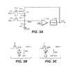
- FIG. 3Aschematically illustrates a charge pump system where a pump 301 supplies an output voltage Vout based upon the output of the comparator 303 .
- the comparatorhas a reference voltage VREF as one input and is connected to a node Nmid of a voltage divider connected to provide feedback from the Vout level.
- the voltage dividerhas a first capacitor C1 307 connected between the Vout level and the Nmid node and a second capacitor C2 305 connected between Nmid and ground.
- the level on Nmidis compared to Vref to control the pump's operation.
- FIGS. 3B and 3CSome of the sources of the leakage are illustrated in FIGS. 3B and 3C .
- FIG. 3Bshows the case of NMOS junction leakage, where a current Beak drains charge off of Nmid to ground for some exemplary values.
- FIG. 3Csimilarly illustrates PMOS junction leakage where the current flows on to Nmid. Due this leakage, the capacitors may eventually need refreshing. This refreshing can be accomplished by opening the switch 311 , connecting the Top node to ground through transistor 313 and the node Nmid to the level Bias through transistor 315 . Once the capacitors are reset, the nodes Top and Nmid can be disconnected from ground and Bias, the switch 311 closed, and the pump can resume operation.
- Vbiascan be taken as OV and Vref as 1.0-1.2V.
- Vbiascan be set at 1.0V-1.2V and Vref can be in the 0-0.2V range.
- the actual levels usedcan be based on the common mode input range of the comparator used in the design.
- FIGS. 4A and 4Billustrate an exemplary embodiment of a circuit to overcome these difficulties.
- FIG. 4Ashows the output of the pump 401 is governed by the output of a comparator 403 that has a reference value Vref at one input and feedback from the output at the other input.
- a comparator 403that has a reference value Vref at one input and feedback from the output at the other input.
- there are two sets of capacitive dividersone formed of capacitors C1 411 and capacitor C2 413 and the other formed of capacitors C3 421 and C4 423 .
- Each of the dividershas its own reset circuit, the switch SW1 415 and transistors 417 and 419 controlled by Vinitl for one and the switch SW2 425 and transistors 427 and 429 controlled by Vinit2 for the other.
- the feedback voltageis switched between the different dividers based on a signal SW supplied to the multiplex circuit 407 .
- the signals SW and well as Vint1, Vint2 and the signals controlling SW1 and SW2can be provided by control circuitry (not illustrated) based, for example, a multiple of some system clock. While one of the dividers is working, the other can be reset.
- the period of the switching (Tswitch)can be determined based on leakage calculations and capacitor size, and derived based on the allowable output error that the system is allowed to tolerate.
- FIG. 4Billustrates an example of the control siganls involved.
- the SW to the multiplex circuitalternates between high (when A is connected) and low (when B is connected) with a period Tswitch.
- the switch SW1 415is closed (SW1 low in FIG. 4B , SW1 is active low) to complete the feedback loop and the transistors 417 and 419 are turned off (Vint1 low).
- the bottom dividercan be reset by openning SW2 425 (SW2 high in FIG. 4B , SW2 is active low) and connecting the Top2 node to ground and Nmid2 to Bias by having Vint2 high.
- the singalsare then swapped to have the bottom loop at B active and the top loops capacitors can be reset.
- FIGS. 4A and 4Billustrate an example using a fairly simple, purely capacitive voltage divider, but the techniques can be applied to other feedback loops that can benefit from periodic refreshing, such as the sort of hybrid arrangement of U.S. Pat. No. 7,554,311.
- the describe approachallows for operations to continue with needing to stop for reset, allowing the systems output to continue under regulation without interruption. Consequently, there is no extra delay or power required for this reason.
- DC-DC convertersare typically optimized for power efficiency for the supplying large load currents. For example, on a non-volatile memory system this requirement is mainly related to AC capacitive current to needed charge up word lines.
- the efficiency of the systemmay drop to extremely low levels, less than 1% in some applications, after the capacitive load is charged up and the load current reduces to just what is needed due to leakage, as is the case during regulation to maintain word line voltages.
- performance requirementsare based on the charging-up period, the system will typically be operating under regulation for a greater amount of time. To improve overall power efficiency, the power efficiency during regulation needs to be improved since it accounts for a significant amount of total operation time.
- FIG. 5illustrates the efficiency of a charge pump system for various load levels.
- the DC-DC converteris optimized for power efficiency for the certain large load current levels, I AC , mainly related to the main task for the pump, such as AC capacitive current to charge up word lines in a memory circuit example.
- I ACload current
- the load currentwill reduce down to the leakage current, I leakage , and the efficiency drops significantly, to possibly even below 1%.
- I leakageis the level needed during regulation to maintain the word line voltage.
- power efficiency during regulationneeds to be improved since it accounts for a significant amount of total operation time. Previous approaches to deal with this problem include improving pump design, adding controls, and so on, but in the end the efficiency is still limited to the DC-DC converter bell shape curve illustrated in FIG. 5 .
- the systemuses an op-amp and AC capacitance to remove the constraints of low pump power efficiency.
- the arrangementuses low bandwidth op-amp feedback and open loop controls to achieve near 100% of power efficiency.
- the added low bandwidth OpAmp, capacitance and switchesare can be minimal in additional area and power consumption.
- the output current of op-ampcan be of the same order as leakage current or noise injection current attenuated by acceptable error in term of the voltage under regulation.
- FIG. 6looks at a fairly typical change pump system of a charge pump 601 connected to receive an oscillator signal OSC and an enable signal ENOSC and provide an output voltage at OUT.
- the ENOSC signalcomes from regulation circuit of a comparator 603 with a gain Av having inputs Vref and the level VMON taken from a node of the capacitive divider formed by the capacitors C1 605 and C3 607 connected between the output node and ground.
- Other forms of voltage dividerscan be used, but here a purely capacitive divider is used as much of the focus here is on reducing current/power consumption. Consequently, the arrangement of FIG. 6 is much the same as in FIG. 3A , but with the reset circuit suppressed.
- the outputis connected to drive a load here schematically represented by the capacitance C WL 611 corresponding the word line capacitance of the exemplary application) that would draw a current I AC and a PN junction 613 taken to represent the leakage component.
- the ratio (Vout/Vref) of the output voltage to the reference valueis given by (Av/(1+Av* ⁇ )), where Av is the gain of the op-amp and ⁇ is the ratio of (sc2) ⁇ 1 /((sc1) ⁇ 1 +(sc2) ⁇ 1 ), with c1, c2 respectively as the capacitances of C1 605, C2 607 and s the transform parameter.
- the load current componentsare taken as having I leakage ⁇ I AC .
- FIG. 7illustrates the behavior of the charge pump system over time in driving the load.
- the capacitive load C WL 611needs to be charged up and, as this is an important factor of device performance, the system is largely optimized for this purpose. This is the initial phase of FIG. 7 , where the I AC indicates this phase.
- the majority of operation for pumpis to maintain the low bandwidth leakage current I leakage .
- Power efficiencyis optimized to be high for the word line settling time, but is extremely low when maintaining the very low leakage current.
- FIGS. 8A and 8Billustrate an exemplary embodiment illustrating a number of the aspects of this section.
- the circuitagain includes the elements of FIG. 6 which are similarly numbered (pump 601 is now 801 and so on), but also includes a unity gain op-amp section.
- a switch SW1 809is added in between the load and charge pump circuits, which can be controlled by the pump comparator output and logic.
- the switch SW2 827is added in the feedback path of the op-amp 821 .
- FIG. 8Aillustrates the setup phase when both of SW1 809 and SW2 827 are closed.
- the low bandwidth op-amp 821 , a capacitor C AC 825 , and a capacitor C 3 823are inserted in the control loop.
- the total quiescent current of these elementsis typically of the same order as I leakage .
- the charge pumpis operating as usual to bring the output level up to the regulation point.
- the output node of the op-amp 821V AC , is biased at a metastable point before Vout reach the target regulation level, where the offset error is sampled into C 3 823 .
- FIG. 8Billustrates the leakage current compensation phase, when op-amp 821 is configured as a comparator.
- the switch SW1 809is opened and the pump related circuits can be turned off to cut off power consumption.
- Switch SW2 827 and the other elements added relative to FIG. 6 (op-amp 821 and capacitors C AC 825 and C 3 823 ) and the feedback network of C1 805 and C2 807maintain the Vout level during regulation and maintain the leakage current and noise injection.
- the comparator 821With the switches open, the comparator 821 will maintain the ratio of (Vout/Vref) as (Av/(1+Av* ⁇ )). As the pump can be disabled, the low pump efficiency during regulation is avoided.
- the op-amp 821is in a unity gain configuration while the pump 801 is ramping up the output the output voltage Vout until it hits the regulation level using the typical pump regulation.
- the switch SW2 827is turned off to configure the op-amp 821 into a comparator; and, as the pump is no longer being used, the switch SW1 809 is also turned off.
- the timing for the switches SW1 809 and SW2 827can be timer controlled, using a fixed amount of time with a margin based upon the design, for example. Alternately the switches can be enabled by the pump enable signal, so that SW1 809 and SW2 827 turn off when pump regulation flag indicates that the regulation level is reached.
- the output VAC of comparator 821will increase and inject I AC until Vout reach the original regulation target, at which point ⁇ Vx return to 0 V.
- VACwill drop and I AC will sink the injected current until Vout reaches the original regulation target.
- the comparator 821will be slewing C AC 825 to maintain Vout. All of the comparator tail current will flow through C AC 825 into Vout to compensate I leakage . In this case, 100% power efficiency can be achieved. If I leakage is smaller than worst case design target, then only a portion of comparator tail current is used to compensate for I leakage and the power efficiency will be correspondingly less than 100%. Consequently, relative to a more conventional DC-DC converter that has low power efficiency under low load current, the arrangement described with respect to FIGS. 8A and 8B can achieve near 100% power efficiency under nominal conditions.
- FIGS. 8A and 8Buse a capacitive divider (C1 805 and C2 807 ) for the feedback network to sample the output voltage as the focus here is on power saving, but other feedback networks can also be used as long the variation of the output signal can be sampled.
- C1 805 and C2 807capacitive divider
- a resistive or hybrid feedback networkexamples of which can be found in the references cited above, can also be used.
- an important aspect of this sectionis using the sampled voltage from output of regulated node with the op-amp 821 is reconfigured as a comparator.
- the comparator's/op-amp's 821 output VACis DC isolated from the charge pump's 801 output, while the AC coupling can be adjusted through the feedback loop to maintain the output voltage.
- the leakage current amplitude, C AC capacitance size, and range of the op-amp output swing rangedetermine the design for application. For example, if the system uses resistive feedback in the feedback network, the high voltage output has two currents going to DC ground, one is related to leakage and then also one due to the regulation current going through the resistor divider. In this case, with same output swing range of the op-amp, a larger C AC capacitor would be required due to the increased DC current through feedback network.
- the aspects presented in this sectioncan present significant improvements in power consumption.
- the use of bi-direction error correction during regulationcan be used for either leakage current or injection noise current. In this way, this arrangement significantly improves the power efficiency from ⁇ 1% using charge pump to near 100%.
- the regulation phasecan be a significant portion of operations in applications such as for read and program operations in NAND memory, the approach presented here can contribute significantly to power efficiency in such operations.
Landscapes
- Engineering & Computer Science (AREA)
- Power Engineering (AREA)
- Dc-Dc Converters (AREA)
Abstract
Description
Qnmid(initital)=Vbias (C1+C2)
while under regulation (assuming the loop gain of charge pump is high enough), Vnmid will be same as VREF. Then:
Qnmid(final)=C1*(Vref−Vout)+C2*Vref
Due to the charge conservation principle,
Vout=(C1+C2)*(Vref−Vbias)/C1.
For example, taking Vbias=0V, Vref=1V, C1=1 pF, and C2=2pF, this gives Vout=(1+2)*(1−0)/1=3V. If charge conservation is not held, then the regulation level on the output will deviate from this target value over time. Interrupting operations for a reset will impact performance. This will waste power as the circuits and voltages need to reset and the restart the system again will need all the voltages to ramp back up to regulation levels.
In the case that Vout is dropping due to Ileakage, then:
ΔVmon=βΔVout
ΔVx=ΔVmon.
The output VAC of
Claims (7)
Priority Applications (1)
| Application Number | Priority Date | Filing Date | Title |
|---|---|---|---|
| US13/929,197US9007046B2 (en) | 2013-06-27 | 2013-06-27 | Efficient high voltage bias regulation circuit |
Applications Claiming Priority (1)
| Application Number | Priority Date | Filing Date | Title |
|---|---|---|---|
| US13/929,197US9007046B2 (en) | 2013-06-27 | 2013-06-27 | Efficient high voltage bias regulation circuit |
Publications (2)
| Publication Number | Publication Date |
|---|---|
| US20150002118A1 US20150002118A1 (en) | 2015-01-01 |
| US9007046B2true US9007046B2 (en) | 2015-04-14 |
Family
ID=52114961
Family Applications (1)
| Application Number | Title | Priority Date | Filing Date |
|---|---|---|---|
| US13/929,197Active2033-11-22US9007046B2 (en) | 2013-06-27 | 2013-06-27 | Efficient high voltage bias regulation circuit |
Country Status (1)
| Country | Link |
|---|---|
| US (1) | US9007046B2 (en) |
Cited By (3)
| Publication number | Priority date | Publication date | Assignee | Title |
|---|---|---|---|---|
| CN110619900A (en)* | 2018-06-19 | 2019-12-27 | 南亚科技股份有限公司 | Pump circuit, dynamic random access memory and control method of overall pump current |
| KR20210085842A (en)* | 2019-12-31 | 2021-07-08 | 삼성전자주식회사 | Memory device |
| US11984156B2 (en) | 2021-05-07 | 2024-05-14 | Samsng Electronics Co., Ltd. | Nonvolatile memory devices having pumping circuits operable in multiple modes |
Families Citing this family (4)
| Publication number | Priority date | Publication date | Assignee | Title |
|---|---|---|---|---|
| US20160261261A1 (en)* | 2015-03-04 | 2016-09-08 | GLF Integrated Power, Inc. | Methods and Apparatus for a Burst Mode Charge Pump Load Switch |
| US10633506B2 (en)* | 2015-09-01 | 2020-04-28 | Stuart D. Frenkel | Reconstituted composite materials derived from waste made by solid state pulverization |
| CN107317570B (en)* | 2016-04-26 | 2023-08-01 | 成都锐成芯微科技股份有限公司 | Common mode level generating circuit |
| US12074577B2 (en)* | 2022-06-27 | 2024-08-27 | Renesas Design Technology Inc. | Active filter |
Citations (217)
| Publication number | Priority date | Publication date | Assignee | Title |
|---|---|---|---|---|
| US3697860A (en) | 1971-03-15 | 1972-10-10 | Westinghouse Electric Corp | Dc static switch circuit with a main switch device and a power sharing circuit portion |
| US4511811A (en) | 1982-02-08 | 1985-04-16 | Seeq Technology, Inc. | Charge pump for providing programming voltage to the word lines in a semiconductor memory array |
| US4583157A (en) | 1985-02-08 | 1986-04-15 | At&T Bell Laboratories | Integrated circuit having a variably boosted node |
| US4636748A (en) | 1985-06-26 | 1987-01-13 | Data General Corporation | Charge pump for use in a phase-locked loop |
| US4736121A (en) | 1985-09-10 | 1988-04-05 | Sos Microelettronica S.p.A. | Charge pump circuit for driving N-channel MOS transistors |
| US4888738A (en) | 1988-06-29 | 1989-12-19 | Seeq Technology | Current-regulated, voltage-regulated erase circuit for EEPROM memory |
| US5140182A (en) | 1989-06-09 | 1992-08-18 | Texas Instruments Incorporated | Plural stage voltage booster circuit with efficient electric charge transfer between successive stages |
| US5168174A (en) | 1991-07-12 | 1992-12-01 | Texas Instruments Incorporated | Negative-voltage charge pump with feedback control |
| US5175706A (en) | 1989-12-07 | 1992-12-29 | Sgs-Thomson Microelectronics S.A. | Programming voltage generator circuit for programmable memory |
| US5263000A (en) | 1992-10-22 | 1993-11-16 | Advanced Micro Devices, Inc. | Drain power supply |
| US5392205A (en) | 1991-11-07 | 1995-02-21 | Motorola, Inc. | Regulated charge pump and method therefor |
| US5436587A (en) | 1993-11-24 | 1995-07-25 | Sundisk Corporation | Charge pump circuit with exponetral multiplication |
| US5483434A (en) | 1992-01-14 | 1996-01-09 | Seesink; Petrus H. | High voltage generator having output current control |
| US5508971A (en) | 1994-10-17 | 1996-04-16 | Sandisk Corporation | Programmable power generation circuit for flash EEPROM memory systems |
| US5521547A (en) | 1992-06-24 | 1996-05-28 | Nec Corporation | Boost voltage generating circuit |
| US5539351A (en) | 1994-11-03 | 1996-07-23 | Gilsdorf; Ben | Circuit and method for reducing a gate volage of a transmission gate within a charge pump circuit |
| US5563779A (en) | 1994-12-05 | 1996-10-08 | Motorola, Inc. | Method and apparatus for a regulated supply on an integrated circuit |
| US5570315A (en) | 1993-09-21 | 1996-10-29 | Kabushiki Kaisha Toshiba | Multi-state EEPROM having write-verify control circuit |
| US5596532A (en) | 1995-10-18 | 1997-01-21 | Sandisk Corporation | Flash EEPROM self-adaptive voltage generation circuit operative within a continuous voltage source range |
| US5602794A (en) | 1995-09-29 | 1997-02-11 | Intel Corporation | Variable stage charge pump |
| US5625544A (en) | 1996-04-25 | 1997-04-29 | Programmable Microelectronics Corp. | Charge pump |
| US5734286A (en) | 1993-05-19 | 1998-03-31 | Kabushiki Kaisha Toshiba | Driving device of charge pump circuit and driving pulse generation method thereof |
| US5801987A (en) | 1997-03-17 | 1998-09-01 | Motorola, Inc. | Automatic transition charge pump for nonvolatile memories |
| US5818766A (en) | 1997-03-05 | 1998-10-06 | Integrated Silicon Solution Inc. | Drain voltage pump circuit for nonvolatile memory device |
| US5828596A (en) | 1996-09-26 | 1998-10-27 | Sharp Kabushiki Kaisha | Semiconductor memory device |
| US5903495A (en) | 1996-03-18 | 1999-05-11 | Kabushiki Kaisha Toshiba | Semiconductor device and memory system |
| US5943226A (en) | 1997-02-27 | 1999-08-24 | Lg Semicon Co., Ltd. | Bootstrap charge pump circuit |
| US5945870A (en) | 1996-07-18 | 1999-08-31 | Altera Corporation | Voltage ramp rate control circuit |
| US5969988A (en) | 1993-08-17 | 1999-10-19 | Kabushiki Kaisha Toshiba | Voltage multiplier circuit and nonvolatile semiconductor memory device having voltage multiplier |
| US5969565A (en) | 1996-05-17 | 1999-10-19 | Nec Corporation | Voltage booster circuit |
| US5973546A (en) | 1996-06-27 | 1999-10-26 | Advanced Micro Devices, Inc. | Charge pump circuit architecture |
| US5982222A (en) | 1995-12-30 | 1999-11-09 | Samsung Electronics, Co., Ltd. | High voltage generating circuit for a semiconductor memory device |
| US6008690A (en) | 1997-06-11 | 1999-12-28 | Nec Corporation | Booster circuit |
| US6018264A (en) | 1998-02-11 | 2000-01-25 | Lg Semicon Co., Ltd. | Pumping circuit with amplitude limited to prevent an over pumping for semiconductor device |
| US6023187A (en) | 1997-12-23 | 2000-02-08 | Mitsubishi Semiconductor America, Inc. | Voltage pump for integrated circuit and operating method thereof |
| US6026002A (en) | 1996-03-28 | 2000-02-15 | Siemens Aktiengesellschaft | Circuit configuration for supplying an electronic load circuit |
| US6104225A (en) | 1997-04-21 | 2000-08-15 | Fujitsu Limited | Semiconductor device using complementary clock and signal input state detection circuit used for the same |
| US6107862A (en) | 1997-02-28 | 2000-08-22 | Seiko Instruments Inc. | Charge pump circuit |
| US6134145A (en) | 1998-06-23 | 2000-10-17 | Sandisk Corporation | High data rate write process for non-volatile flash memories |
| US6147566A (en) | 1996-12-30 | 2000-11-14 | Sgs-Thomson Microelectronics S.A. | Oscillator and switch-over control circuit for a high-voltage generator |
| US6151229A (en) | 1999-06-30 | 2000-11-21 | Intel Corporation | Charge pump with gated pumped output diode at intermediate stage |
| US6154088A (en) | 1996-07-18 | 2000-11-28 | Micron Technology, Inc. | Clocking scheme and charge transfer switch for increasing the efficiency of a charge pump or other circuit |
| US6157242A (en) | 1998-03-19 | 2000-12-05 | Sharp Kabushiki Kaisha | Charge pump for operation at a wide range of power supply voltages |
| WO2001006336A1 (en) | 1999-07-15 | 2001-01-25 | Maxim Integrated Products, Inc. | Pulse frequency operation of regulated charge pumps |
| US6188590B1 (en) | 1996-12-18 | 2001-02-13 | Macronix International Co., Ltd. | Regulator system for charge pump circuits |
| US6198645B1 (en) | 1998-07-02 | 2001-03-06 | National Semiconductor Corporation | Buck and boost switched capacitor gain stage with optional shared rest state |
| US6208198B1 (en) | 1998-10-27 | 2001-03-27 | Hyundai Electronics Industries Co., Ltd. | Drain voltage pumping circuit |
| US6249898B1 (en) | 1998-06-30 | 2001-06-19 | Synopsys, Inc. | Method and system for reliability analysis of CMOS VLSI circuits based on stage partitioning and node activities |
| US6249445B1 (en) | 1999-02-15 | 2001-06-19 | Nec Corporation | Booster including charge pumping circuit with its electric power consumption reduced and method of operating the same |
| US6275096B1 (en) | 1999-12-14 | 2001-08-14 | International Business Machines Corporation | Charge pump system having multiple independently activated charge pumps and corresponding method |
| US6278294B1 (en) | 1997-05-01 | 2001-08-21 | Mitsubishi Denki Kabushiki Kaisha | Output buffer circuit |
| US6285622B1 (en) | 1999-10-29 | 2001-09-04 | Mitsubishi Denki Kabushiki Kaisha | Semiconductor device |
| US6297687B1 (en) | 1998-08-11 | 2001-10-02 | Oki Electric Industry Co., Ltd. | Drive control circuit of charged pump circuit |
| US6314025B1 (en) | 1998-06-23 | 2001-11-06 | Sandisk Corporation | High data rate write process for non-volatile flash memories |
| US6320428B1 (en) | 1997-02-26 | 2001-11-20 | Kabushiki Kaisha Toshiba | Semiconductor integrated circuit device |
| US6320796B1 (en) | 2000-11-10 | 2001-11-20 | Marvell International, Ltd. | Variable slope charge pump control |
| US6329869B1 (en) | 1999-05-19 | 2001-12-11 | Nec Corporation | Semiconductor device with less influence of noise |
| US20020008566A1 (en) | 2000-07-18 | 2002-01-24 | Mitsubishi Denki Kabushiki Kaisha And Mitsubishi Electric Engineering Company Limited | Internal Voltage generation circuit |
| US6344959B1 (en) | 1998-05-01 | 2002-02-05 | Unitrode Corporation | Method for sensing the output voltage of a charge pump circuit without applying a load to the output stage |
| US6344984B1 (en) | 1999-09-03 | 2002-02-05 | Nec Corporation | Voltage multiplier having an intermediate tap |
| US20020014908A1 (en) | 1998-12-21 | 2002-02-07 | Christl Lauterbach | Device for voltage multiplication with high efficiency, combination of the device with a battery-operated apparatus, and low-power loss generation of a programming voltage |
| US6356062B1 (en) | 2000-09-27 | 2002-03-12 | Intel Corporation | Degenerative load temperature correction for charge pumps |
| US6359798B1 (en) | 2000-12-08 | 2002-03-19 | Samsung Electronics Co., Ltd. | Charge pump voltage converter |
| US6369642B1 (en) | 2000-12-26 | 2002-04-09 | Intel Corporation | Output switch for charge pump reconfiguration |
| US6370075B1 (en) | 1998-06-30 | 2002-04-09 | Sandisk Corporation | Charge pump circuit adjustable in response to an external voltage source |
| US6385107B1 (en) | 1999-11-12 | 2002-05-07 | Stmicroelectronics S.R.L. | Architecture for handling internal voltages in a non-volatile memory, particularly in a single-voltage supply type of dual-work flash memory |
| US6400202B1 (en) | 2000-02-10 | 2002-06-04 | International Business Machines Corporation | Programmable delay element and synchronous DRAM using the same |
| US6404274B1 (en) | 1998-04-09 | 2002-06-11 | Kabushiki Kaisha Toshiba | Internal voltage generating circuit capable of generating variable multi-level voltages |
| US20020075706A1 (en) | 1990-04-06 | 2002-06-20 | Mosaid Technologies Incorporated | Boosted voltage supply |
| US20020075063A1 (en) | 2000-12-18 | 2002-06-20 | Hitachi America, Ltd. | Frequency adaptive negative voltage generator |
| US6411157B1 (en) | 2000-06-29 | 2002-06-25 | International Business Machines Corporation | Self-refresh on-chip voltage generator |
| US6424570B1 (en) | 2001-06-26 | 2002-07-23 | Advanced Micro Devices, Inc. | Modulated charge pump with uses an analog to digital converter to compensate for supply voltage variations |
| US6445243B2 (en) | 2000-05-10 | 2002-09-03 | Sanyo Electric Co., Ltd. | Charge-pump circuit and control method thereof |
| US20020130704A1 (en) | 2001-02-01 | 2002-09-19 | Takao Myono | Charge pump circuit |
| US20020130701A1 (en) | 2001-03-16 | 2002-09-19 | Matrix Semiconductor, Inc. | Multi-stage charge pump |
| US6456170B1 (en) | 1999-06-01 | 2002-09-24 | Fujitsu Limited | Comparator and voltage controlled oscillator circuit |
| US20020140463A1 (en) | 2001-03-15 | 2002-10-03 | Paul Cheung | Programmable soft-start control for charge pump |
| US6476666B1 (en) | 2001-05-30 | 2002-11-05 | Alliance Semiconductor Corporation | Bootstrapped charge pump |
| US6518830B2 (en) | 2000-08-22 | 2003-02-11 | Stmicroelectronics S.R.L. | High efficiency electronic circuit for generating and regulating a supply voltage |
| US6522191B1 (en) | 1997-04-21 | 2003-02-18 | Hynix Semiconductor, Inc. | Synchronized voltage generator for amplifying voltage inputs |
| US6525949B1 (en) | 2000-12-22 | 2003-02-25 | Matrix Semiconductor, Inc. | Charge pump circuit |
| US6525614B2 (en) | 2000-11-17 | 2003-02-25 | Sanyo Electric Co., Ltd. | Voltage boost system having feedback control |
| US6531792B2 (en) | 2001-04-10 | 2003-03-11 | Fujitsu Limited | DC-DC converter and storage apparatus |
| US6538930B2 (en) | 2001-01-09 | 2003-03-25 | Mitsubishi Denki Kabushiki Kaisha | Charge pump circuit for generating positive and negative voltage with reverse current prevention circuit and a nonvolatile memory using the same |
| US6545529B2 (en) | 2000-05-02 | 2003-04-08 | Hynix Semiconductor Inc. | High voltage generating circuit |
| US6577535B2 (en) | 2001-02-16 | 2003-06-10 | Sandisk Corporation | Method and system for distributed power generation in multi-chip memory systems |
| US20030128560A1 (en) | 2002-01-10 | 2003-07-10 | Saiki William John | High voltage generation and regulation system for digital multilevel nonvolatile memory |
| US6606267B2 (en) | 1998-06-23 | 2003-08-12 | Sandisk Corporation | High data rate write process for non-volatile flash memories |
| US20030214346A1 (en) | 2002-02-25 | 2003-11-20 | Stmicroelectronics S.R.I. | Charge pump for negative voltages |
| US6661682B2 (en) | 2001-02-16 | 2003-12-09 | Imec (Interuniversitair Microelectronica Centrum) | High voltage generating charge pump circuit |
| US6703891B2 (en) | 1999-05-17 | 2004-03-09 | Hitachi, Ltd. | Charge pump with improved reliability |
| US20040046603A1 (en) | 2002-09-06 | 2004-03-11 | Lorenzo Bedarida | Modular charge pump architecture |
| US6724241B1 (en) | 2002-10-25 | 2004-04-20 | Atmel Corporation | Variable charge pump circuit with dynamic load |
| US6734718B1 (en) | 2002-12-23 | 2004-05-11 | Sandisk Corporation | High voltage ripple reduction |
| US6737907B2 (en) | 2001-07-03 | 2004-05-18 | International Business Machines Corporation | Programmable DC voltage generator system |
| US6762640B2 (en) | 2002-04-24 | 2004-07-13 | Nec Electronics Corporation | Bias voltage generating circuit and semiconductor integrated circuit device |
| US6781440B2 (en) | 2002-02-18 | 2004-08-24 | Winbond Electronics Corp. | Charge pump circuit with voltage multiplier for boosting clock signal and method thereof |
| US6798274B2 (en) | 2002-03-27 | 2004-09-28 | Sanyo Electric Co., Ltd. | Booster and imaging device using booster |
| US6834001B2 (en) | 2001-09-26 | 2004-12-21 | Sanyo Electric Co., Ltd. | Multi-stage switched capacitor DC-DC converter |
| US20050024125A1 (en) | 2003-08-01 | 2005-02-03 | Mcnitt John L. | Highly efficient, high current drive, multi-phase voltage multiplier |
| US20050030088A1 (en) | 2003-08-07 | 2005-02-10 | Raul-Adrian Cernea | Area efficient charge pump |
| US6859091B1 (en) | 2003-09-18 | 2005-02-22 | Maxim Integrated Products, Inc. | Continuous linear regulated zero dropout charge pump with high efficiency load predictive clocking scheme |
| US6878981B2 (en) | 2003-03-20 | 2005-04-12 | Tower Semiconductor Ltd. | Triple-well charge pump stage with no threshold voltage back-bias effect |
| US20050093614A1 (en) | 2003-10-30 | 2005-05-05 | Dong-Uk Lee | Multi stage voltage pump circuit |
| US6891764B2 (en) | 2003-04-11 | 2005-05-10 | Intel Corporation | Apparatus and method to read a nonvolatile memory |
| US6894554B2 (en) | 2002-01-17 | 2005-05-17 | Seiko Epson Corporation | Step-up circuits |
| US6927441B2 (en) | 2001-03-20 | 2005-08-09 | Stmicroelectronics S.R.L. | Variable stage charge pump |
| US6933768B2 (en) | 2002-06-20 | 2005-08-23 | Infineon Technologies Ag | Method for increasing the input voltage of an integrated circuit with a two-stage charge pump, and integrated circuit |
| US20050195017A1 (en) | 2004-03-03 | 2005-09-08 | Tien-Tzu Chen | High efficiency charge pump with prevention from reverse current |
| US6954386B2 (en) | 2002-02-21 | 2005-10-11 | Elpida Memory, Inc. | Boosted potential generation circuit and control method |
| US20050248386A1 (en) | 2004-05-10 | 2005-11-10 | Sandisk Corporation | Four phase charge pump operable without phase overlap with improved efficiency |
| US6975135B1 (en) | 2002-12-10 | 2005-12-13 | Altera Corporation | Universally programmable output buffer |
| US6985397B2 (en) | 2003-03-26 | 2006-01-10 | Sharp Kabushiki Kaisha | Semiconductor storage device and portable electronic equipment having the same |
| US6990031B2 (en) | 2001-09-03 | 2006-01-24 | Elpida Memory, Inc. | Semiconductor memory device control method and semiconductor memory device |
| US7002381B1 (en) | 2001-12-11 | 2006-02-21 | Advanced Micro Devices, Inc. | Switched-capacitor controller to control the rise times of on-chip generated high voltages |
| US7023260B2 (en) | 2003-06-30 | 2006-04-04 | Matrix Semiconductor, Inc. | Charge pump circuit incorporating corresponding parallel charge pump stages and method therefor |
| US20060114053A1 (en) | 2004-11-30 | 2006-06-01 | Renesas Technology Corp. | Charge-pump-type power supply circuit |
| US20060119393A1 (en) | 2004-12-02 | 2006-06-08 | National Chiao Tung University | Power gating structure having data retention and intermediate modes |
| US7092263B2 (en) | 2004-04-02 | 2006-08-15 | Au Optronics Corp. | DC-DC converter for converting an input voltage to a first output voltage |
| US7116154B2 (en) | 2003-08-06 | 2006-10-03 | Spansion Llc | Low power charge pump |
| US7120051B2 (en) | 2004-12-14 | 2006-10-10 | Sandisk Corporation | Pipelined programming of non-volatile memories using early data |
| US7123078B2 (en) | 2002-10-07 | 2006-10-17 | Hynix Semiconductor Inc. | Boosting voltage control circuit |
| US7129759B2 (en) | 2004-02-03 | 2006-10-31 | Nec Electronics Corporation | Integrated circuit including an overvoltage protection circuit |
| US20060244518A1 (en) | 2005-04-29 | 2006-11-02 | Hynix Semiconductor Inc. | Internal voltage generator |
| US20060250177A1 (en) | 2005-05-09 | 2006-11-09 | Thorp Tyler J | Methods and apparatus for dynamically reconfiguring a charge pump during output transients |
| US7135911B2 (en) | 2000-05-24 | 2006-11-14 | Kabushiki Kaisha Toshiba | Potential detector and semiconductor integrated circuit |
| US7135910B2 (en) | 2002-09-27 | 2006-11-14 | Sandisk Corporation | Charge pump with fibonacci number multiplication |
| US20070001745A1 (en) | 2005-06-29 | 2007-01-04 | Chih-Jen Yen | Charge pump for generating arbitrary voltage levels |
| JP2007020268A (en) | 2005-07-06 | 2007-01-25 | Casio Comput Co Ltd | Power circuit |
| WO2006132757A3 (en) | 2005-06-03 | 2007-02-22 | Atmel Corp | High efficiency bi-directional charge pump circuit |
| US20070053216A1 (en) | 2005-09-02 | 2007-03-08 | Texas Instruments Incorporated | Three-phase low noise charge pump and method |
| US20070069805A1 (en) | 2005-09-29 | 2007-03-29 | Hynix Semiconductor Inc. | Internal voltage generating circuit |
| US7205682B2 (en) | 2003-03-14 | 2007-04-17 | Oki Electric Industry Co., Ltd. | Internal power supply circuit |
| US7208996B2 (en) | 2004-03-26 | 2007-04-24 | Sanyo Electric Co., Ltd. | Charge pump circuit |
| US7215179B2 (en) | 2002-11-18 | 2007-05-08 | Renesas Technology Corp. | Booster circuit |
| US7224591B2 (en) | 2005-02-24 | 2007-05-29 | Sharp Kabushiki Kaisha | Charge pump DC/DC converter circuit |
| US7227780B2 (en) | 2004-11-30 | 2007-06-05 | Spansion Llc | Semiconductor device and control method thereof |
| US20070126494A1 (en) | 2005-12-06 | 2007-06-07 | Sandisk Corporation | Charge pump having shunt diode for improved operating efficiency |
| US20070139100A1 (en) | 2005-12-16 | 2007-06-21 | Sandisk Corporation | Voltage regulation with active supplemental current for output stabilization |
| US20070139099A1 (en)* | 2005-12-16 | 2007-06-21 | Sandisk Corporation | Charge pump regulation control for improved power efficiency |
| US7239192B2 (en) | 2003-08-06 | 2007-07-03 | Stmicroelectronics Sa | Self-reparable device to generate a high voltage, and method for repairing a device to generate a high voltage |
| US7253676B2 (en) | 2003-12-25 | 2007-08-07 | Kabushiki Kaisha Toshiba | Semiconductor device and driving method of semiconductor device |
| US7253675B2 (en) | 2005-03-08 | 2007-08-07 | Texas Instruments Incorporated | Bootstrapping circuit capable of sampling inputs beyond supply voltage |
| US7259612B2 (en) | 2005-06-28 | 2007-08-21 | Atmel Corporation | Efficient charge pump for a wide range of supply voltages |
| US20070211502A1 (en) | 2006-03-07 | 2007-09-13 | Kunihiro Komiya | Voltage step-up circuit and electric appliance therewith |
| US20070210853A1 (en) | 2006-03-13 | 2007-09-13 | Kabushiki Kaisha Toshiba | Voltage generation circuit and semiconductor memory using the same |
| US20070222498A1 (en) | 2006-03-24 | 2007-09-27 | Freescale Semiconductor Inc. | Slew rate control of a charge pump |
| US7276960B2 (en) | 2005-07-18 | 2007-10-02 | Dialog Semiconductor Gmbh | Voltage regulated charge pump with regulated charge current into the flying capacitor |
| US20070229149A1 (en) | 2006-03-30 | 2007-10-04 | Sandisk Corporation | Voltage regulator having high voltage protection |
| US20080024096A1 (en)* | 2006-07-31 | 2008-01-31 | Sandisk Corporation | Hybrid charge pump regulation |
| US20080024198A1 (en) | 2006-07-28 | 2008-01-31 | Stmicroelectronics S.R.I. | Voltage booster |
| US20080068067A1 (en)* | 2006-09-19 | 2008-03-20 | Sandisk Corporation | Implementation of output floating scheme for hv charge pumps |
| US20080111604A1 (en) | 2005-03-17 | 2008-05-15 | Boerstler David W | Digital circuit to measure and/or correct duty cycles |
| US20080116963A1 (en) | 2006-11-20 | 2008-05-22 | Hynix Semiconductor Inc. | Clock control circuit and voltage pumping device using the same |
| US20080136500A1 (en) | 2006-12-11 | 2008-06-12 | Atmel Corporation | Charge pump for generation of multiple output-voltage levels |
| US20080157852A1 (en) | 2006-12-29 | 2008-07-03 | Sandisk Corporation | Unified voltage generation apparatus with improved power efficiency |
| US20080157731A1 (en)* | 2007-01-01 | 2008-07-03 | Sandisk Corp. | Generation of Analog Voltage Using Self-Biased Capacitive Feedback Stage |
| DE102007026290A1 (en) | 2006-12-28 | 2008-07-03 | Samsung Electronics Co., Ltd., Suwon | High voltage generating circuit, has regulator generating high voltage measuring current for measuring high voltage depending on level of high voltage, for controlling control signal, and for generating activation signal |
| US20080157859A1 (en) | 2006-12-29 | 2008-07-03 | Sandisk Corporation | Unified voltage generation method with improved power efficiency |
| US7397677B1 (en) | 2006-02-08 | 2008-07-08 | National Semiconductor Corporation | Apparatus and method for charge pump control with adjustable series resistance |
| US20080218134A1 (en) | 2007-03-08 | 2008-09-11 | Matsushita Electric Industrial Co., Ltd. | Power supply apparatus |
| US20080239856A1 (en) | 2007-03-30 | 2008-10-02 | Tyler Thorp | Method for Load-Based Voltage Generation |
| US20080239802A1 (en) | 2007-03-30 | 2008-10-02 | Tyler Thorp | Device with Load-Based Voltage Generation |
| US20080278222A1 (en) | 2006-07-19 | 2008-11-13 | Stmicroelectronics S.R.I. | Charge pump circuit |
| US20080307342A1 (en) | 2007-06-08 | 2008-12-11 | Apple Inc. | Rendering Semi-Transparent User Interface Elements |
| US7468628B2 (en) | 2004-11-08 | 2008-12-23 | Hynix Semiconductor Inc. | Internal voltage generators for semiconductor memory device |
| US20090033306A1 (en) | 2007-08-02 | 2009-02-05 | Toru Tanzawa | Voltage trimming |
| US7495500B2 (en) | 2006-12-31 | 2009-02-24 | Sandisk 3D Llc | Method for using a multiple polarity reversible charge pump circuit |
| US20090051413A1 (en) | 2007-08-20 | 2009-02-26 | Taiwan Semiconductor Manufacturing Company, Ltd. | Apparatus and method for increasing charge pump efficiency |
| US20090058507A1 (en) | 2007-08-28 | 2009-03-05 | Prajit Nandi | Bottom Plate Regulated Charge Pump |
| US20090058506A1 (en) | 2007-08-28 | 2009-03-05 | Prajit Nandi | Bottom Plate Regulation of Charge Pumps |
| US20090091366A1 (en) | 2007-10-09 | 2009-04-09 | Hynix Semiconductor, Inc. | Voltage generator of semiconductor integrated circuit |
| US7521978B2 (en) | 2005-11-02 | 2009-04-21 | Hynix Semiconductor Inc. | Clock driver |
| US20090121780A1 (en) | 2007-11-12 | 2009-05-14 | Macronix International Co., Ltd. | Multiple-stage charge pump with charge recycle circuit |
| US20090153231A1 (en) | 2007-12-12 | 2009-06-18 | Feng Pan | Diode Connected Regulation of Charge Pumps |
| US20090153230A1 (en) | 2007-12-12 | 2009-06-18 | Feng Pan | Low Voltage Charge Pump with Regulation |
| US20090153232A1 (en) | 2007-05-25 | 2009-06-18 | Atmel Corporation | Low voltage charge pump |
| US20090167418A1 (en) | 2007-10-24 | 2009-07-02 | Vijay Raghavan | Supply Regulated Charge Pump System |
| US20090174441A1 (en) | 2008-01-08 | 2009-07-09 | Gebara Fadi H | Peak Power Reduction Methods in Distributed Charge Pump Systems |
| US20090184697A1 (en) | 2008-01-23 | 2009-07-23 | Micron Technology, Inc. | System, apparatus, and method for selectable voltage regulation |
| US7579903B2 (en) | 2005-08-03 | 2009-08-25 | Nec Electronics Corporation | Power-source potential control circuit and method of trimming power-source potential |
| US20090219077A1 (en) | 2008-02-29 | 2009-09-03 | Stefano Pietri | Voltage multiplier with improved efficiency |
| US20090315616A1 (en) | 2008-06-24 | 2009-12-24 | Qui Vi Nguyen | Clock Generator Circuit for a Charge Pump |
| US20090322413A1 (en) | 2008-06-25 | 2009-12-31 | Huynh Jonathan H | Techniques of Ripple Reduction for Charge Pumps |
| US20100019832A1 (en) | 2008-06-09 | 2010-01-28 | Feng Pan | Self-Adaptive Multi-Stage Charge Pump |
| US20100033232A1 (en) | 2008-08-11 | 2010-02-11 | Micron Technology, Inc. | Variable stage charge pump and method for providing boosted output voltage |
| US7667529B2 (en) | 2007-11-07 | 2010-02-23 | Orlando Consuelo | Charge pump warm-up current reduction |
| US7671572B2 (en) | 2006-04-07 | 2010-03-02 | Samsung Electronics Co. Ltd. | Voltage boost circuit and voltage boosting method using voltage boost clock signal with varying frequency |
| US20100074034A1 (en) | 2008-09-23 | 2010-03-25 | Marco Cazzaniga | Voltage regulator with reduced sensitivity of output voltage to change in load current |
| US20100085794A1 (en) | 2008-10-06 | 2010-04-08 | Yingchang Chen | Set and reset detection circuits for reversible resistance switching memory material |
| US7696812B2 (en) | 2006-12-31 | 2010-04-13 | Sandisk 3D Llc | Cooperative charge pump circuit and method |
| US7795952B2 (en) | 2008-12-17 | 2010-09-14 | Sandisk Corporation | Regulation of recovery rates in charge pumps |
| US20100244935A1 (en) | 2007-11-05 | 2010-09-30 | Electronics And Telecommunications Research Institute | High-voltage cmos charge pump |
| US7830203B2 (en) | 2007-10-05 | 2010-11-09 | Industrial Technology Research Institute | System-on-a-chip and power gating circuit thereof |
| US20100302877A1 (en) | 2009-05-29 | 2010-12-02 | Samsung Electronics Co., Ltd. | Memory device having reduced standby current and memory system including same |
| US20110026329A1 (en) | 2009-08-03 | 2011-02-03 | Renesas Electronics Corporation | Semiconductor device using charge pump circuit |
| US7928796B2 (en) | 2008-06-23 | 2011-04-19 | Kabushiki Kaisha Toshiba | Constant voltage boost power supply |
| US7944277B1 (en) | 2008-01-04 | 2011-05-17 | Marvell International Ltd. | Circuit and methods of adaptive charge-pump regulation |
| US7956675B2 (en) | 2008-09-08 | 2011-06-07 | Rohm Co., Ltd. | Control circuit and control method for charge pump circuit |
| US20110133821A1 (en) | 2009-12-04 | 2011-06-09 | Renesas Electronics Corporation | Charge pump circuit |
| US20110156803A1 (en) | 2009-12-31 | 2011-06-30 | Stmicroelectronics Asia Pacific Pte Ltd. | Method for generating multiple incremental output voltages using a single charge pump chain |
| US7973592B2 (en)* | 2009-07-21 | 2011-07-05 | Sandisk Corporation | Charge pump with current based regulation |
| US20110254615A1 (en) | 2010-04-20 | 2011-10-20 | Qualcomm Incorporated | Pll charge pump with reduced coupling to bias nodes |
| US8093953B2 (en) | 2009-03-20 | 2012-01-10 | Analog Devices, Inc. | Amplifier system with digital adaptive power boost |
| US8159091B2 (en) | 2009-04-01 | 2012-04-17 | Chimei Innolux Corporation | Switch circuit of DC/DC converter configured to conduct various modes for charging/discharging |
| US8193853B2 (en)* | 2009-06-22 | 2012-06-05 | Richtek Technology Corp. | Efficiency and thermal improvement of a charge pump by mixing different input voltages |
| US8242834B2 (en) | 2009-07-14 | 2012-08-14 | Novatek Microelectronics Corp. | Charge pump circuit |
| US20120230071A1 (en) | 2011-03-10 | 2012-09-13 | Semiconductor Components Industries, Llc | Power supply circuit system |
| US20120274394A1 (en)* | 2011-04-27 | 2012-11-01 | Realtek Semiconductor Corp. | Charge pump feedback control device and method using the same |
| US8339183B2 (en) | 2009-07-24 | 2012-12-25 | Sandisk Technologies Inc. | Charge pump with reduced energy consumption through charge sharing and clock boosting suitable for high voltage word line in flash memories |
| US8395440B2 (en) | 2010-11-23 | 2013-03-12 | Arm Limited | Apparatus and method for controlling power gating in an integrated circuit |
| US8400212B1 (en)* | 2011-09-22 | 2013-03-19 | Sandisk Technologies Inc. | High voltage charge pump regulation system with fine step adjustment |
| US20130181521A1 (en)* | 2010-09-29 | 2013-07-18 | Rf Micro Devices, Inc | Single +82 c-buckboost converter with multiple regulated supply outputs |
| US8604868B2 (en) | 2011-04-01 | 2013-12-10 | Stmicroelectronics S.R.L. | Dynamic biasing circuit for a protection stage using low voltage transistors |
| US8643358B2 (en) | 2010-07-09 | 2014-02-04 | Hynix Semiconductor Inc. | Oscillator |
| US20140085985A1 (en)* | 2012-09-27 | 2014-03-27 | Sandisk Technologies Inc. | Sigma Delta Over-Sampling Charge Pump Analog-To-Digital Converter |
| US20140375293A1 (en)* | 2013-06-25 | 2014-12-25 | Sandisk Technologies Inc. | Capacitive Regulation of Charge Pumps Without Refresh Operation Interruption |
- 2013
- 2013-06-27USUS13/929,197patent/US9007046B2/enactiveActive
Patent Citations (248)
| Publication number | Priority date | Publication date | Assignee | Title |
|---|---|---|---|---|
| US3697860A (en) | 1971-03-15 | 1972-10-10 | Westinghouse Electric Corp | Dc static switch circuit with a main switch device and a power sharing circuit portion |
| US4511811A (en) | 1982-02-08 | 1985-04-16 | Seeq Technology, Inc. | Charge pump for providing programming voltage to the word lines in a semiconductor memory array |
| US4583157A (en) | 1985-02-08 | 1986-04-15 | At&T Bell Laboratories | Integrated circuit having a variably boosted node |
| US4636748A (en) | 1985-06-26 | 1987-01-13 | Data General Corporation | Charge pump for use in a phase-locked loop |
| US4736121A (en) | 1985-09-10 | 1988-04-05 | Sos Microelettronica S.p.A. | Charge pump circuit for driving N-channel MOS transistors |
| US4888738A (en) | 1988-06-29 | 1989-12-19 | Seeq Technology | Current-regulated, voltage-regulated erase circuit for EEPROM memory |
| US5140182A (en) | 1989-06-09 | 1992-08-18 | Texas Instruments Incorporated | Plural stage voltage booster circuit with efficient electric charge transfer between successive stages |
| US5175706A (en) | 1989-12-07 | 1992-12-29 | Sgs-Thomson Microelectronics S.A. | Programming voltage generator circuit for programmable memory |
| US20020075706A1 (en) | 1990-04-06 | 2002-06-20 | Mosaid Technologies Incorporated | Boosted voltage supply |
| US5168174A (en) | 1991-07-12 | 1992-12-01 | Texas Instruments Incorporated | Negative-voltage charge pump with feedback control |
| US5392205A (en) | 1991-11-07 | 1995-02-21 | Motorola, Inc. | Regulated charge pump and method therefor |
| US5483434A (en) | 1992-01-14 | 1996-01-09 | Seesink; Petrus H. | High voltage generator having output current control |
| US5521547A (en) | 1992-06-24 | 1996-05-28 | Nec Corporation | Boost voltage generating circuit |
| US5263000A (en) | 1992-10-22 | 1993-11-16 | Advanced Micro Devices, Inc. | Drain power supply |
| US5734286A (en) | 1993-05-19 | 1998-03-31 | Kabushiki Kaisha Toshiba | Driving device of charge pump circuit and driving pulse generation method thereof |
| US5969988A (en) | 1993-08-17 | 1999-10-19 | Kabushiki Kaisha Toshiba | Voltage multiplier circuit and nonvolatile semiconductor memory device having voltage multiplier |
| US5570315A (en) | 1993-09-21 | 1996-10-29 | Kabushiki Kaisha Toshiba | Multi-state EEPROM having write-verify control circuit |
| US5436587A (en) | 1993-11-24 | 1995-07-25 | Sundisk Corporation | Charge pump circuit with exponetral multiplication |
| US5693570A (en) | 1994-10-17 | 1997-12-02 | Sandisk Corporation | Process for manufacturing a programmable power generation circuit for flash EEPROM memory systems |
| US5592420A (en) | 1994-10-17 | 1997-01-07 | Sandisk Corporation | Programmable power generation circuit for flash EEPROM memory systems |
| US5563825A (en) | 1994-10-17 | 1996-10-08 | Sandisk Corporation | Programmable power generation circuit for flash eeprom memory systems |
| US5568424A (en) | 1994-10-17 | 1996-10-22 | Sandisk Corporation | Programmable power generation circuit for flash EEPROM memory systems |
| US5621685A (en) | 1994-10-17 | 1997-04-15 | Sandisk Corporation | Programmable power generation circuit for flash EEPROM memory systems |
| US5508971A (en) | 1994-10-17 | 1996-04-16 | Sandisk Corporation | Programmable power generation circuit for flash EEPROM memory systems |
| US5539351A (en) | 1994-11-03 | 1996-07-23 | Gilsdorf; Ben | Circuit and method for reducing a gate volage of a transmission gate within a charge pump circuit |
| US5563779A (en) | 1994-12-05 | 1996-10-08 | Motorola, Inc. | Method and apparatus for a regulated supply on an integrated circuit |
| US5732039A (en) | 1995-09-29 | 1998-03-24 | Intel Corporation | Variable stage charge pump |
| US5767735A (en) | 1995-09-29 | 1998-06-16 | Intel Corporation | Variable stage charge pump |
| US5781473A (en) | 1995-09-29 | 1998-07-14 | Intel Corporation | Variable stage charge pump |
| US5602794A (en) | 1995-09-29 | 1997-02-11 | Intel Corporation | Variable stage charge pump |
| US5596532A (en) | 1995-10-18 | 1997-01-21 | Sandisk Corporation | Flash EEPROM self-adaptive voltage generation circuit operative within a continuous voltage source range |
| US5982222A (en) | 1995-12-30 | 1999-11-09 | Samsung Electronics, Co., Ltd. | High voltage generating circuit for a semiconductor memory device |
| US6046935A (en) | 1996-03-18 | 2000-04-04 | Kabushiki Kaisha Toshiba | Semiconductor device and memory system |
| US5903495A (en) | 1996-03-18 | 1999-05-11 | Kabushiki Kaisha Toshiba | Semiconductor device and memory system |
| US6026002A (en) | 1996-03-28 | 2000-02-15 | Siemens Aktiengesellschaft | Circuit configuration for supplying an electronic load circuit |
| US5625544A (en) | 1996-04-25 | 1997-04-29 | Programmable Microelectronics Corp. | Charge pump |
| US5969565A (en) | 1996-05-17 | 1999-10-19 | Nec Corporation | Voltage booster circuit |
| US5973546A (en) | 1996-06-27 | 1999-10-26 | Advanced Micro Devices, Inc. | Charge pump circuit architecture |
| US5945870A (en) | 1996-07-18 | 1999-08-31 | Altera Corporation | Voltage ramp rate control circuit |
| US6307425B1 (en) | 1996-07-18 | 2001-10-23 | Micron Technology, Inc. | Clocking scheme and charge transfer switch for increasing the efficiency of a charge pump or other circuit |
| US6154088A (en) | 1996-07-18 | 2000-11-28 | Micron Technology, Inc. | Clocking scheme and charge transfer switch for increasing the efficiency of a charge pump or other circuit |
| US5828596A (en) | 1996-09-26 | 1998-10-27 | Sharp Kabushiki Kaisha | Semiconductor memory device |
| US6188590B1 (en) | 1996-12-18 | 2001-02-13 | Macronix International Co., Ltd. | Regulator system for charge pump circuits |
| US6147566A (en) | 1996-12-30 | 2000-11-14 | Sgs-Thomson Microelectronics S.A. | Oscillator and switch-over control circuit for a high-voltage generator |
| US6320428B1 (en) | 1997-02-26 | 2001-11-20 | Kabushiki Kaisha Toshiba | Semiconductor integrated circuit device |
| US5943226A (en) | 1997-02-27 | 1999-08-24 | Lg Semicon Co., Ltd. | Bootstrap charge pump circuit |
| US6107862A (en) | 1997-02-28 | 2000-08-22 | Seiko Instruments Inc. | Charge pump circuit |
| US5818766A (en) | 1997-03-05 | 1998-10-06 | Integrated Silicon Solution Inc. | Drain voltage pump circuit for nonvolatile memory device |
| US5801987A (en) | 1997-03-17 | 1998-09-01 | Motorola, Inc. | Automatic transition charge pump for nonvolatile memories |
| US6104225A (en) | 1997-04-21 | 2000-08-15 | Fujitsu Limited | Semiconductor device using complementary clock and signal input state detection circuit used for the same |
| US6522191B1 (en) | 1997-04-21 | 2003-02-18 | Hynix Semiconductor, Inc. | Synchronized voltage generator for amplifying voltage inputs |
| US6278294B1 (en) | 1997-05-01 | 2001-08-21 | Mitsubishi Denki Kabushiki Kaisha | Output buffer circuit |
| US6008690A (en) | 1997-06-11 | 1999-12-28 | Nec Corporation | Booster circuit |
| US6023187A (en) | 1997-12-23 | 2000-02-08 | Mitsubishi Semiconductor America, Inc. | Voltage pump for integrated circuit and operating method thereof |
| US6018264A (en) | 1998-02-11 | 2000-01-25 | Lg Semicon Co., Ltd. | Pumping circuit with amplitude limited to prevent an over pumping for semiconductor device |
| US6157242A (en) | 1998-03-19 | 2000-12-05 | Sharp Kabushiki Kaisha | Charge pump for operation at a wide range of power supply voltages |
| US6404274B1 (en) | 1998-04-09 | 2002-06-11 | Kabushiki Kaisha Toshiba | Internal voltage generating circuit capable of generating variable multi-level voltages |
| US6344959B1 (en) | 1998-05-01 | 2002-02-05 | Unitrode Corporation | Method for sensing the output voltage of a charge pump circuit without applying a load to the output stage |
| US6314025B1 (en) | 1998-06-23 | 2001-11-06 | Sandisk Corporation | High data rate write process for non-volatile flash memories |
| US6606267B2 (en) | 1998-06-23 | 2003-08-12 | Sandisk Corporation | High data rate write process for non-volatile flash memories |
| US6944058B2 (en) | 1998-06-23 | 2005-09-13 | Sandisk Corporation | High data rate write process for non-volatile flash memories |
| US6134145A (en) | 1998-06-23 | 2000-10-17 | Sandisk Corporation | High data rate write process for non-volatile flash memories |
| US6556465B2 (en) | 1998-06-30 | 2003-04-29 | Sandisk Corporation | Adjustable circuits for analog or multi-level memory |
| US6760262B2 (en) | 1998-06-30 | 2004-07-06 | Sandisk Corporation | Charge pump circuit adjustable in response to an external voltage source |
| US6370075B1 (en) | 1998-06-30 | 2002-04-09 | Sandisk Corporation | Charge pump circuit adjustable in response to an external voltage source |
| US6249898B1 (en) | 1998-06-30 | 2001-06-19 | Synopsys, Inc. | Method and system for reliability analysis of CMOS VLSI circuits based on stage partitioning and node activities |
| US6198645B1 (en) | 1998-07-02 | 2001-03-06 | National Semiconductor Corporation | Buck and boost switched capacitor gain stage with optional shared rest state |
| US6297687B1 (en) | 1998-08-11 | 2001-10-02 | Oki Electric Industry Co., Ltd. | Drive control circuit of charged pump circuit |
| US6456154B2 (en) | 1998-08-11 | 2002-09-24 | Oki Electric Industry Co., Ltd. | Drive control circuit of charged pump circuit |
| US6208198B1 (en) | 1998-10-27 | 2001-03-27 | Hyundai Electronics Industries Co., Ltd. | Drain voltage pumping circuit |
| US20020014908A1 (en) | 1998-12-21 | 2002-02-07 | Christl Lauterbach | Device for voltage multiplication with high efficiency, combination of the device with a battery-operated apparatus, and low-power loss generation of a programming voltage |
| US6249445B1 (en) | 1999-02-15 | 2001-06-19 | Nec Corporation | Booster including charge pumping circuit with its electric power consumption reduced and method of operating the same |
| US6703891B2 (en) | 1999-05-17 | 2004-03-09 | Hitachi, Ltd. | Charge pump with improved reliability |
| US6329869B1 (en) | 1999-05-19 | 2001-12-11 | Nec Corporation | Semiconductor device with less influence of noise |
| US6456170B1 (en) | 1999-06-01 | 2002-09-24 | Fujitsu Limited | Comparator and voltage controlled oscillator circuit |
| US6151229A (en) | 1999-06-30 | 2000-11-21 | Intel Corporation | Charge pump with gated pumped output diode at intermediate stage |
| WO2001006336A1 (en) | 1999-07-15 | 2001-01-25 | Maxim Integrated Products, Inc. | Pulse frequency operation of regulated charge pumps |
| US6344984B1 (en) | 1999-09-03 | 2002-02-05 | Nec Corporation | Voltage multiplier having an intermediate tap |
| US6285622B1 (en) | 1999-10-29 | 2001-09-04 | Mitsubishi Denki Kabushiki Kaisha | Semiconductor device |
| US6385107B1 (en) | 1999-11-12 | 2002-05-07 | Stmicroelectronics S.R.L. | Architecture for handling internal voltages in a non-volatile memory, particularly in a single-voltage supply type of dual-work flash memory |
| US6275096B1 (en) | 1999-12-14 | 2001-08-14 | International Business Machines Corporation | Charge pump system having multiple independently activated charge pumps and corresponding method |
| US6400202B1 (en) | 2000-02-10 | 2002-06-04 | International Business Machines Corporation | Programmable delay element and synchronous DRAM using the same |
| US6545529B2 (en) | 2000-05-02 | 2003-04-08 | Hynix Semiconductor Inc. | High voltage generating circuit |
| US6445243B2 (en) | 2000-05-10 | 2002-09-03 | Sanyo Electric Co., Ltd. | Charge-pump circuit and control method thereof |
| US7135911B2 (en) | 2000-05-24 | 2006-11-14 | Kabushiki Kaisha Toshiba | Potential detector and semiconductor integrated circuit |
| US6411157B1 (en) | 2000-06-29 | 2002-06-25 | International Business Machines Corporation | Self-refresh on-chip voltage generator |
| US20020008566A1 (en) | 2000-07-18 | 2002-01-24 | Mitsubishi Denki Kabushiki Kaisha And Mitsubishi Electric Engineering Company Limited | Internal Voltage generation circuit |
| US6518830B2 (en) | 2000-08-22 | 2003-02-11 | Stmicroelectronics S.R.L. | High efficiency electronic circuit for generating and regulating a supply voltage |
| US6356062B1 (en) | 2000-09-27 | 2002-03-12 | Intel Corporation | Degenerative load temperature correction for charge pumps |
| US6320796B1 (en) | 2000-11-10 | 2001-11-20 | Marvell International, Ltd. | Variable slope charge pump control |
| US6525614B2 (en) | 2000-11-17 | 2003-02-25 | Sanyo Electric Co., Ltd. | Voltage boost system having feedback control |
| US6359798B1 (en) | 2000-12-08 | 2002-03-19 | Samsung Electronics Co., Ltd. | Charge pump voltage converter |
| US20020075063A1 (en) | 2000-12-18 | 2002-06-20 | Hitachi America, Ltd. | Frequency adaptive negative voltage generator |
| US6525949B1 (en) | 2000-12-22 | 2003-02-25 | Matrix Semiconductor, Inc. | Charge pump circuit |
| US6369642B1 (en) | 2000-12-26 | 2002-04-09 | Intel Corporation | Output switch for charge pump reconfiguration |
| US6538930B2 (en) | 2001-01-09 | 2003-03-25 | Mitsubishi Denki Kabushiki Kaisha | Charge pump circuit for generating positive and negative voltage with reverse current prevention circuit and a nonvolatile memory using the same |
| US20020130704A1 (en) | 2001-02-01 | 2002-09-19 | Takao Myono | Charge pump circuit |
| US6577535B2 (en) | 2001-02-16 | 2003-06-10 | Sandisk Corporation | Method and system for distributed power generation in multi-chip memory systems |
| US6661682B2 (en) | 2001-02-16 | 2003-12-09 | Imec (Interuniversitair Microelectronica Centrum) | High voltage generating charge pump circuit |
| US20020140463A1 (en) | 2001-03-15 | 2002-10-03 | Paul Cheung | Programmable soft-start control for charge pump |
| US6486728B2 (en) | 2001-03-16 | 2002-11-26 | Matrix Semiconductor, Inc. | Multi-stage charge pump |
| US20020130701A1 (en) | 2001-03-16 | 2002-09-19 | Matrix Semiconductor, Inc. | Multi-stage charge pump |
| US6927441B2 (en) | 2001-03-20 | 2005-08-09 | Stmicroelectronics S.R.L. | Variable stage charge pump |
| US6531792B2 (en) | 2001-04-10 | 2003-03-11 | Fujitsu Limited | DC-DC converter and storage apparatus |
| US6476666B1 (en) | 2001-05-30 | 2002-11-05 | Alliance Semiconductor Corporation | Bootstrapped charge pump |
| US6424570B1 (en) | 2001-06-26 | 2002-07-23 | Advanced Micro Devices, Inc. | Modulated charge pump with uses an analog to digital converter to compensate for supply voltage variations |
| US6737907B2 (en) | 2001-07-03 | 2004-05-18 | International Business Machines Corporation | Programmable DC voltage generator system |
| US6990031B2 (en) | 2001-09-03 | 2006-01-24 | Elpida Memory, Inc. | Semiconductor memory device control method and semiconductor memory device |
| US6834001B2 (en) | 2001-09-26 | 2004-12-21 | Sanyo Electric Co., Ltd. | Multi-stage switched capacitor DC-DC converter |
| US7002381B1 (en) | 2001-12-11 | 2006-02-21 | Advanced Micro Devices, Inc. | Switched-capacitor controller to control the rise times of on-chip generated high voltages |
| US20030128560A1 (en) | 2002-01-10 | 2003-07-10 | Saiki William John | High voltage generation and regulation system for digital multilevel nonvolatile memory |
| US6894554B2 (en) | 2002-01-17 | 2005-05-17 | Seiko Epson Corporation | Step-up circuits |
| US6781440B2 (en) | 2002-02-18 | 2004-08-24 | Winbond Electronics Corp. | Charge pump circuit with voltage multiplier for boosting clock signal and method thereof |
| US6954386B2 (en) | 2002-02-21 | 2005-10-11 | Elpida Memory, Inc. | Boosted potential generation circuit and control method |
| US6819162B2 (en) | 2002-02-25 | 2004-11-16 | Stmicroelectronics S.R.L. | Charge pump for negative voltages |
| US20030214346A1 (en) | 2002-02-25 | 2003-11-20 | Stmicroelectronics S.R.I. | Charge pump for negative voltages |
| US6798274B2 (en) | 2002-03-27 | 2004-09-28 | Sanyo Electric Co., Ltd. | Booster and imaging device using booster |
| US6762640B2 (en) | 2002-04-24 | 2004-07-13 | Nec Electronics Corporation | Bias voltage generating circuit and semiconductor integrated circuit device |
| US6933768B2 (en) | 2002-06-20 | 2005-08-23 | Infineon Technologies Ag | Method for increasing the input voltage of an integrated circuit with a two-stage charge pump, and integrated circuit |
| US20040046603A1 (en) | 2002-09-06 | 2004-03-11 | Lorenzo Bedarida | Modular charge pump architecture |
| US7135910B2 (en) | 2002-09-27 | 2006-11-14 | Sandisk Corporation | Charge pump with fibonacci number multiplication |
| US7123078B2 (en) | 2002-10-07 | 2006-10-17 | Hynix Semiconductor Inc. | Boosting voltage control circuit |
| US6724241B1 (en) | 2002-10-25 | 2004-04-20 | Atmel Corporation | Variable charge pump circuit with dynamic load |
| US7215179B2 (en) | 2002-11-18 | 2007-05-08 | Renesas Technology Corp. | Booster circuit |
| US6975135B1 (en) | 2002-12-10 | 2005-12-13 | Altera Corporation | Universally programmable output buffer |
| US7116155B2 (en) | 2002-12-23 | 2006-10-03 | Sandisk Corporation | High voltage ripple reduction and substrate protection |
| US6734718B1 (en) | 2002-12-23 | 2004-05-11 | Sandisk Corporation | High voltage ripple reduction |
| US7205682B2 (en) | 2003-03-14 | 2007-04-17 | Oki Electric Industry Co., Ltd. | Internal power supply circuit |
| US6878981B2 (en) | 2003-03-20 | 2005-04-12 | Tower Semiconductor Ltd. | Triple-well charge pump stage with no threshold voltage back-bias effect |
| US6985397B2 (en) | 2003-03-26 | 2006-01-10 | Sharp Kabushiki Kaisha | Semiconductor storage device and portable electronic equipment having the same |
| US6891764B2 (en) | 2003-04-11 | 2005-05-10 | Intel Corporation | Apparatus and method to read a nonvolatile memory |
| US7023260B2 (en) | 2003-06-30 | 2006-04-04 | Matrix Semiconductor, Inc. | Charge pump circuit incorporating corresponding parallel charge pump stages and method therefor |
| US20050024125A1 (en) | 2003-08-01 | 2005-02-03 | Mcnitt John L. | Highly efficient, high current drive, multi-phase voltage multiplier |
| US7116154B2 (en) | 2003-08-06 | 2006-10-03 | Spansion Llc | Low power charge pump |
| US7239192B2 (en) | 2003-08-06 | 2007-07-03 | Stmicroelectronics Sa | Self-reparable device to generate a high voltage, and method for repairing a device to generate a high voltage |
| US20050237103A1 (en) | 2003-08-07 | 2005-10-27 | Raul-Adrian Cernea | Area efficient charge pump |
| US20050030088A1 (en) | 2003-08-07 | 2005-02-10 | Raul-Adrian Cernea | Area efficient charge pump |
| US6922096B2 (en) | 2003-08-07 | 2005-07-26 | Sandisk Corporation | Area efficient charge pump |
| US7113023B2 (en) | 2003-08-07 | 2006-09-26 | Sandisk Corporation | Area efficient charge pump |
| US6859091B1 (en) | 2003-09-18 | 2005-02-22 | Maxim Integrated Products, Inc. | Continuous linear regulated zero dropout charge pump with high efficiency load predictive clocking scheme |
| US20050093614A1 (en) | 2003-10-30 | 2005-05-05 | Dong-Uk Lee | Multi stage voltage pump circuit |
| US7253676B2 (en) | 2003-12-25 | 2007-08-07 | Kabushiki Kaisha Toshiba | Semiconductor device and driving method of semiconductor device |
| US7129759B2 (en) | 2004-02-03 | 2006-10-31 | Nec Electronics Corporation | Integrated circuit including an overvoltage protection circuit |
| US20050195017A1 (en) | 2004-03-03 | 2005-09-08 | Tien-Tzu Chen | High efficiency charge pump with prevention from reverse current |
| US6995603B2 (en) | 2004-03-03 | 2006-02-07 | Aimtron Technology Corp. | High efficiency charge pump with prevention from reverse current |
| US7208996B2 (en) | 2004-03-26 | 2007-04-24 | Sanyo Electric Co., Ltd. | Charge pump circuit |
| US7092263B2 (en) | 2004-04-02 | 2006-08-15 | Au Optronics Corp. | DC-DC converter for converting an input voltage to a first output voltage |
| US20050248386A1 (en) | 2004-05-10 | 2005-11-10 | Sandisk Corporation | Four phase charge pump operable without phase overlap with improved efficiency |
| US7030683B2 (en) | 2004-05-10 | 2006-04-18 | Sandisk Corporation | Four phase charge pump operable without phase overlap with improved efficiency |
| US7468628B2 (en) | 2004-11-08 | 2008-12-23 | Hynix Semiconductor Inc. | Internal voltage generators for semiconductor memory device |
| US20060114053A1 (en) | 2004-11-30 | 2006-06-01 | Renesas Technology Corp. | Charge-pump-type power supply circuit |
| US7227780B2 (en) | 2004-11-30 | 2007-06-05 | Spansion Llc | Semiconductor device and control method thereof |
| US20060119393A1 (en) | 2004-12-02 | 2006-06-08 | National Chiao Tung University | Power gating structure having data retention and intermediate modes |
| US7345928B2 (en) | 2004-12-14 | 2008-03-18 | Sandisk Corporation | Data recovery methods in multi-state memory after program fail |
| US7120051B2 (en) | 2004-12-14 | 2006-10-10 | Sandisk Corporation | Pipelined programming of non-volatile memories using early data |
| US7224591B2 (en) | 2005-02-24 | 2007-05-29 | Sharp Kabushiki Kaisha | Charge pump DC/DC converter circuit |
| US7253675B2 (en) | 2005-03-08 | 2007-08-07 | Texas Instruments Incorporated | Bootstrapping circuit capable of sampling inputs beyond supply voltage |
| US20080111604A1 (en) | 2005-03-17 | 2008-05-15 | Boerstler David W | Digital circuit to measure and/or correct duty cycles |
| US20060244518A1 (en) | 2005-04-29 | 2006-11-02 | Hynix Semiconductor Inc. | Internal voltage generator |
| US20060250177A1 (en) | 2005-05-09 | 2006-11-09 | Thorp Tyler J | Methods and apparatus for dynamically reconfiguring a charge pump during output transients |
| WO2006132757A3 (en) | 2005-06-03 | 2007-02-22 | Atmel Corp | High efficiency bi-directional charge pump circuit |
| US20080042731A1 (en) | 2005-06-03 | 2008-02-21 | Atmel Corporation | High efficiency bi-directional charge pump circuit |
| US7259612B2 (en) | 2005-06-28 | 2007-08-21 | Atmel Corporation | Efficient charge pump for a wide range of supply voltages |
| US20070001745A1 (en) | 2005-06-29 | 2007-01-04 | Chih-Jen Yen | Charge pump for generating arbitrary voltage levels |
| US7279957B2 (en) | 2005-06-29 | 2007-10-09 | Novatek Microelectronics Corp. | Charge pump for generating arbitrary voltage levels |
| JP2007020268A (en) | 2005-07-06 | 2007-01-25 | Casio Comput Co Ltd | Power circuit |
| US7276960B2 (en) | 2005-07-18 | 2007-10-02 | Dialog Semiconductor Gmbh | Voltage regulated charge pump with regulated charge current into the flying capacitor |
| US7579903B2 (en) | 2005-08-03 | 2009-08-25 | Nec Electronics Corporation | Power-source potential control circuit and method of trimming power-source potential |
| US20070053216A1 (en) | 2005-09-02 | 2007-03-08 | Texas Instruments Incorporated | Three-phase low noise charge pump and method |
| US20070069805A1 (en) | 2005-09-29 | 2007-03-29 | Hynix Semiconductor Inc. | Internal voltage generating circuit |
| US7521978B2 (en) | 2005-11-02 | 2009-04-21 | Hynix Semiconductor Inc. | Clock driver |
| US20070126494A1 (en) | 2005-12-06 | 2007-06-07 | Sandisk Corporation | Charge pump having shunt diode for improved operating efficiency |
| US20070139099A1 (en)* | 2005-12-16 | 2007-06-21 | Sandisk Corporation | Charge pump regulation control for improved power efficiency |
| US20070139100A1 (en) | 2005-12-16 | 2007-06-21 | Sandisk Corporation | Voltage regulation with active supplemental current for output stabilization |
| US7397677B1 (en) | 2006-02-08 | 2008-07-08 | National Semiconductor Corporation | Apparatus and method for charge pump control with adjustable series resistance |
| US20070211502A1 (en) | 2006-03-07 | 2007-09-13 | Kunihiro Komiya | Voltage step-up circuit and electric appliance therewith |
| US20070210853A1 (en) | 2006-03-13 | 2007-09-13 | Kabushiki Kaisha Toshiba | Voltage generation circuit and semiconductor memory using the same |
| US20070222498A1 (en) | 2006-03-24 | 2007-09-27 | Freescale Semiconductor Inc. | Slew rate control of a charge pump |
| US20070229149A1 (en) | 2006-03-30 | 2007-10-04 | Sandisk Corporation | Voltage regulator having high voltage protection |
| US7671572B2 (en) | 2006-04-07 | 2010-03-02 | Samsung Electronics Co. Ltd. | Voltage boost circuit and voltage boosting method using voltage boost clock signal with varying frequency |
| US20080278222A1 (en) | 2006-07-19 | 2008-11-13 | Stmicroelectronics S.R.I. | Charge pump circuit |
| US20080024198A1 (en) | 2006-07-28 | 2008-01-31 | Stmicroelectronics S.R.I. | Voltage booster |
| US20080024096A1 (en)* | 2006-07-31 | 2008-01-31 | Sandisk Corporation | Hybrid charge pump regulation |
| US7554311B2 (en) | 2006-07-31 | 2009-06-30 | Sandisk Corporation | Hybrid charge pump regulation |
| US7368979B2 (en) | 2006-09-19 | 2008-05-06 | Sandisk Corporation | Implementation of output floating scheme for hv charge pumps |
| US20080068067A1 (en)* | 2006-09-19 | 2008-03-20 | Sandisk Corporation | Implementation of output floating scheme for hv charge pumps |
| US7772914B2 (en) | 2006-11-20 | 2010-08-10 | Hynix Semiconductor Inc. | Clock control circuit and voltage pumping device using the same |
| US20080116963A1 (en) | 2006-11-20 | 2008-05-22 | Hynix Semiconductor Inc. | Clock control circuit and voltage pumping device using the same |
| US7579902B2 (en) | 2006-12-11 | 2009-08-25 | Atmel Corporation | Charge pump for generation of multiple output-voltage levels |
| US20080136500A1 (en) | 2006-12-11 | 2008-06-12 | Atmel Corporation | Charge pump for generation of multiple output-voltage levels |
| DE102007026290A1 (en) | 2006-12-28 | 2008-07-03 | Samsung Electronics Co., Ltd., Suwon | High voltage generating circuit, has regulator generating high voltage measuring current for measuring high voltage depending on level of high voltage, for controlling control signal, and for generating activation signal |
| US20080157859A1 (en) | 2006-12-29 | 2008-07-03 | Sandisk Corporation | Unified voltage generation method with improved power efficiency |
| US20080157852A1 (en) | 2006-12-29 | 2008-07-03 | Sandisk Corporation | Unified voltage generation apparatus with improved power efficiency |
| US7495500B2 (en) | 2006-12-31 | 2009-02-24 | Sandisk 3D Llc | Method for using a multiple polarity reversible charge pump circuit |
| US7696812B2 (en) | 2006-12-31 | 2010-04-13 | Sandisk 3D Llc | Cooperative charge pump circuit and method |
| US20080157731A1 (en)* | 2007-01-01 | 2008-07-03 | Sandisk Corp. | Generation of Analog Voltage Using Self-Biased Capacitive Feedback Stage |
| US20080218134A1 (en) | 2007-03-08 | 2008-09-11 | Matsushita Electric Industrial Co., Ltd. | Power supply apparatus |
| US20080239802A1 (en) | 2007-03-30 | 2008-10-02 | Tyler Thorp | Device with Load-Based Voltage Generation |
| US20080239856A1 (en) | 2007-03-30 | 2008-10-02 | Tyler Thorp | Method for Load-Based Voltage Generation |
| US20090153232A1 (en) | 2007-05-25 | 2009-06-18 | Atmel Corporation | Low voltage charge pump |
| US20080307342A1 (en) | 2007-06-08 | 2008-12-11 | Apple Inc. | Rendering Semi-Transparent User Interface Elements |
| US20090033306A1 (en) | 2007-08-02 | 2009-02-05 | Toru Tanzawa | Voltage trimming |
| US20090051413A1 (en) | 2007-08-20 | 2009-02-26 | Taiwan Semiconductor Manufacturing Company, Ltd. | Apparatus and method for increasing charge pump efficiency |
| US20090058507A1 (en) | 2007-08-28 | 2009-03-05 | Prajit Nandi | Bottom Plate Regulated Charge Pump |
| US20090058506A1 (en) | 2007-08-28 | 2009-03-05 | Prajit Nandi | Bottom Plate Regulation of Charge Pumps |
| US7830203B2 (en) | 2007-10-05 | 2010-11-09 | Industrial Technology Research Institute | System-on-a-chip and power gating circuit thereof |
| US20090091366A1 (en) | 2007-10-09 | 2009-04-09 | Hynix Semiconductor, Inc. | Voltage generator of semiconductor integrated circuit |
| US20090167418A1 (en) | 2007-10-24 | 2009-07-02 | Vijay Raghavan | Supply Regulated Charge Pump System |
| US20100244935A1 (en) | 2007-11-05 | 2010-09-30 | Electronics And Telecommunications Research Institute | High-voltage cmos charge pump |
| US7667529B2 (en) | 2007-11-07 | 2010-02-23 | Orlando Consuelo | Charge pump warm-up current reduction |
| US20090121780A1 (en) | 2007-11-12 | 2009-05-14 | Macronix International Co., Ltd. | Multiple-stage charge pump with charge recycle circuit |
| US20090153231A1 (en) | 2007-12-12 | 2009-06-18 | Feng Pan | Diode Connected Regulation of Charge Pumps |
| US20090153230A1 (en) | 2007-12-12 | 2009-06-18 | Feng Pan | Low Voltage Charge Pump with Regulation |
| US7944277B1 (en) | 2008-01-04 | 2011-05-17 | Marvell International Ltd. | Circuit and methods of adaptive charge-pump regulation |
| US20090174441A1 (en) | 2008-01-08 | 2009-07-09 | Gebara Fadi H | Peak Power Reduction Methods in Distributed Charge Pump Systems |
| US20090184697A1 (en) | 2008-01-23 | 2009-07-23 | Micron Technology, Inc. | System, apparatus, and method for selectable voltage regulation |
| US20090219077A1 (en) | 2008-02-29 | 2009-09-03 | Stefano Pietri | Voltage multiplier with improved efficiency |
| US7602233B2 (en) | 2008-02-29 | 2009-10-13 | Freescale Semiconductor, Inc. | Voltage multiplier with improved efficiency |
| US20100019832A1 (en) | 2008-06-09 | 2010-01-28 | Feng Pan | Self-Adaptive Multi-Stage Charge Pump |
| US7928796B2 (en) | 2008-06-23 | 2011-04-19 | Kabushiki Kaisha Toshiba | Constant voltage boost power supply |
| US20090315616A1 (en) | 2008-06-24 | 2009-12-24 | Qui Vi Nguyen | Clock Generator Circuit for a Charge Pump |
| US20090322413A1 (en) | 2008-06-25 | 2009-12-31 | Huynh Jonathan H | Techniques of Ripple Reduction for Charge Pumps |
| US20100033232A1 (en) | 2008-08-11 | 2010-02-11 | Micron Technology, Inc. | Variable stage charge pump and method for providing boosted output voltage |
| US7956675B2 (en) | 2008-09-08 | 2011-06-07 | Rohm Co., Ltd. | Control circuit and control method for charge pump circuit |
| US20100074034A1 (en) | 2008-09-23 | 2010-03-25 | Marco Cazzaniga | Voltage regulator with reduced sensitivity of output voltage to change in load current |
| US20100085794A1 (en) | 2008-10-06 | 2010-04-08 | Yingchang Chen | Set and reset detection circuits for reversible resistance switching memory material |
| US7795952B2 (en) | 2008-12-17 | 2010-09-14 | Sandisk Corporation | Regulation of recovery rates in charge pumps |
| US8093953B2 (en) | 2009-03-20 | 2012-01-10 | Analog Devices, Inc. | Amplifier system with digital adaptive power boost |
| US8159091B2 (en) | 2009-04-01 | 2012-04-17 | Chimei Innolux Corporation | Switch circuit of DC/DC converter configured to conduct various modes for charging/discharging |
| US20100302877A1 (en) | 2009-05-29 | 2010-12-02 | Samsung Electronics Co., Ltd. | Memory device having reduced standby current and memory system including same |
| US8193853B2 (en)* | 2009-06-22 | 2012-06-05 | Richtek Technology Corp. | Efficiency and thermal improvement of a charge pump by mixing different input voltages |
| US8242834B2 (en) | 2009-07-14 | 2012-08-14 | Novatek Microelectronics Corp. | Charge pump circuit |
| US7973592B2 (en)* | 2009-07-21 | 2011-07-05 | Sandisk Corporation | Charge pump with current based regulation |
| US8339183B2 (en) | 2009-07-24 | 2012-12-25 | Sandisk Technologies Inc. | Charge pump with reduced energy consumption through charge sharing and clock boosting suitable for high voltage word line in flash memories |
| US20110026329A1 (en) | 2009-08-03 | 2011-02-03 | Renesas Electronics Corporation | Semiconductor device using charge pump circuit |
| US20110133821A1 (en) | 2009-12-04 | 2011-06-09 | Renesas Electronics Corporation | Charge pump circuit |
| US20110156803A1 (en) | 2009-12-31 | 2011-06-30 | Stmicroelectronics Asia Pacific Pte Ltd. | Method for generating multiple incremental output voltages using a single charge pump chain |
| US20110254615A1 (en) | 2010-04-20 | 2011-10-20 | Qualcomm Incorporated | Pll charge pump with reduced coupling to bias nodes |
| US8643358B2 (en) | 2010-07-09 | 2014-02-04 | Hynix Semiconductor Inc. | Oscillator |
| US20130181521A1 (en)* | 2010-09-29 | 2013-07-18 | Rf Micro Devices, Inc | Single +82 c-buckboost converter with multiple regulated supply outputs |
| US8395440B2 (en) | 2010-11-23 | 2013-03-12 | Arm Limited | Apparatus and method for controlling power gating in an integrated circuit |
| US20120230071A1 (en) | 2011-03-10 | 2012-09-13 | Semiconductor Components Industries, Llc | Power supply circuit system |
| US8604868B2 (en) | 2011-04-01 | 2013-12-10 | Stmicroelectronics S.R.L. | Dynamic biasing circuit for a protection stage using low voltage transistors |
| US20120274394A1 (en)* | 2011-04-27 | 2012-11-01 | Realtek Semiconductor Corp. | Charge pump feedback control device and method using the same |
| US20130162229A1 (en) | 2011-04-27 | 2013-06-27 | Realtek Semiconductor Corp. | Charge pump feedback control device and method using the same |
| US8400212B1 (en)* | 2011-09-22 | 2013-03-19 | Sandisk Technologies Inc. | High voltage charge pump regulation system with fine step adjustment |
| US20140085985A1 (en)* | 2012-09-27 | 2014-03-27 | Sandisk Technologies Inc. | Sigma Delta Over-Sampling Charge Pump Analog-To-Digital Converter |
| US20140375293A1 (en)* | 2013-06-25 | 2014-12-25 | Sandisk Technologies Inc. | Capacitive Regulation of Charge Pumps Without Refresh Operation Interruption |
Non-Patent Citations (4)
| Title |
|---|
| Ang et al., "An On-Chip Voltage Regulator Using Switched Decoupling Capacitors," 2000 IEEE International Solid-State Circuits Conference, 2 pages. |
| Feng Pan et al., "Charge Pump Circuit Design", McGraw-Hill, 2006, 26 pages. |
| U.S. Appl. No. 12/506,998 entitled "Charge Pump with Current Based Regulation" filed Jul. 21, 2009, 21 pages. |
| U.S. Appl. No. 12/634,385 entitled "Multi-Stage Charge Pump with Variable Number of Boosting Stages" filed Dec. 9, 2009, 33 pages. |
Cited By (6)
| Publication number | Priority date | Publication date | Assignee | Title |
|---|---|---|---|---|
| CN110619900A (en)* | 2018-06-19 | 2019-12-27 | 南亚科技股份有限公司 | Pump circuit, dynamic random access memory and control method of overall pump current |
| CN110619900B (en)* | 2018-06-19 | 2021-08-27 | 南亚科技股份有限公司 | Pump circuit, dynamic random access memory and control method of overall pump current |
| KR20210085842A (en)* | 2019-12-31 | 2021-07-08 | 삼성전자주식회사 | Memory device |
| US11127474B2 (en) | 2019-12-31 | 2021-09-21 | Samsung Electronics Co., Ltd. | Memory device |
| US11636901B2 (en) | 2019-12-31 | 2023-04-25 | Samsung Electronics Co., Ltd. | Memory device |
| US11984156B2 (en) | 2021-05-07 | 2024-05-14 | Samsng Electronics Co., Ltd. | Nonvolatile memory devices having pumping circuits operable in multiple modes |
Also Published As
| Publication number | Publication date |
|---|---|
| US20150002118A1 (en) | 2015-01-01 |
Similar Documents
| Publication | Publication Date | Title |
|---|---|---|
| US9077238B2 (en) | Capacitive regulation of charge pumps without refresh operation interruption | |
| US9007046B2 (en) | Efficient high voltage bias regulation circuit | |
| US20240223077A1 (en) | Start-up of step-up power converter with switched-capacitor network | |
| CN102043417B (en) | Low dropout voltage regulator, DC-to-DC converter, and method for low dropout voltage regulation | |
| US9444340B2 (en) | Circuits and methods for providing current to a load | |
| US8098089B2 (en) | Voltage booster | |
| CN113346742B (en) | Device for providing low-power charge pump for integrated circuit | |
| US8248150B2 (en) | Passive bootstrapped charge pump for NMOS power device based regulators | |
| US9013229B2 (en) | Charge pump circuit | |
| US6617832B1 (en) | Low ripple scalable DC-to-DC converter circuit | |
| US7940118B1 (en) | Dying gasp charge controller | |
| US7990205B2 (en) | Semiconductor integrated circuit with switching variable resistance device | |
| US9680371B2 (en) | Charge pumps having variable gain and variable frequency | |
| US9154027B2 (en) | Dynamic load matching charge pump for reduced current consumption | |
| CN211046760U (en) | Charge pump circuit and nonvolatile memory device | |
| US11616440B2 (en) | DC/DC voltage converter and method | |
| US20160261261A1 (en) | Methods and Apparatus for a Burst Mode Charge Pump Load Switch | |
| CN101951144A (en) | Efficient charge pump and working method thereof | |
| US9548656B1 (en) | Low voltage ripple charge pump with shared capacitor oscillator | |
| CN111465910B (en) | Voltage regulator with voltage slope detector and method thereof | |
| Racape et al. | A PMOS-switch based charge pump, allowing lost cost implementation on a CMOS standard process | |
| US10338619B2 (en) | Voltage regulator with performance compensation | |
| KR102291175B1 (en) | Charge pump circuit, semiconductor device, and semiconductor memory device | |
| US12046987B2 (en) | Voltage regulator circuit for a switching circuit load | |
| JP2005204366A (en) | Dc-dc converter |
Legal Events
| Date | Code | Title | Description |
|---|---|---|---|
| AS | Assignment | Owner name:SANDISK TECHNOLOGIES INC., TEXAS Free format text:ASSIGNMENT OF ASSIGNORS INTEREST;ASSIGNOR:PAN, FENG;REEL/FRAME:030726/0853 Effective date:20130627 | |
| STCF | Information on status: patent grant | Free format text:PATENTED CASE | |
| AS | Assignment | Owner name:SANDISK TECHNOLOGIES LLC, TEXAS Free format text:CHANGE OF NAME;ASSIGNOR:SANDISK TECHNOLOGIES INC;REEL/FRAME:038807/0948 Effective date:20160516 | |
| MAFP | Maintenance fee payment | Free format text:PAYMENT OF MAINTENANCE FEE, 4TH YEAR, LARGE ENTITY (ORIGINAL EVENT CODE: M1551); ENTITY STATUS OF PATENT OWNER: LARGE ENTITY Year of fee payment:4 | |
| MAFP | Maintenance fee payment | Free format text:PAYMENT OF MAINTENANCE FEE, 8TH YEAR, LARGE ENTITY (ORIGINAL EVENT CODE: M1552); ENTITY STATUS OF PATENT OWNER: LARGE ENTITY Year of fee payment:8 | |
| AS | Assignment | Owner name:SANDISK TECHNOLOGIES, INC., CALIFORNIA Free format text:ASSIGNMENT OF ASSIGNORS INTEREST;ASSIGNOR:SANDISK TECHNOLOGIES LLC;REEL/FRAME:069796/0423 Effective date:20241227 | |
| AS | Assignment | Owner name:SANDISK TECHNOLOGIES, INC., CALIFORNIA Free format text:PARTIAL RELEASE OF SECURITY INTERESTS;ASSIGNOR:JPMORGAN CHASE BANK, N.A., AS AGENT;REEL/FRAME:071382/0001 Effective date:20250424 Owner name:JPMORGAN CHASE BANK, N.A., AS COLLATERAL AGENT, ILLINOIS Free format text:SECURITY AGREEMENT;ASSIGNOR:SANDISK TECHNOLOGIES, INC.;REEL/FRAME:071050/0001 Effective date:20250424 |