US9006060B2 - N-type field effect transistors, arrays comprising N-type vertically-oriented transistors, methods of forming an N-type field effect transistor, and methods of forming an array comprising vertically-oriented N-type transistors - Google Patents
N-type field effect transistors, arrays comprising N-type vertically-oriented transistors, methods of forming an N-type field effect transistor, and methods of forming an array comprising vertically-oriented N-type transistorsDownload PDFInfo
- Publication number
- US9006060B2 US9006060B2US13/591,073US201213591073AUS9006060B2US 9006060 B2US9006060 B2US 9006060B2US 201213591073 AUS201213591073 AUS 201213591073AUS 9006060 B2US9006060 B2US 9006060B2
- Authority
- US
- United States
- Prior art keywords
- silicon
- semiconductor material
- conductivity
- source
- drain region
- Prior art date
- Legal status (The legal status is an assumption and is not a legal conclusion. Google has not performed a legal analysis and makes no representation as to the accuracy of the status listed.)
- Active, expires
Links
- 238000000034methodMethods0.000titleclaimsabstractdescription69
- 230000005669field effectEffects0.000titleclaimsabstractdescription33
- 238000003491arrayMethods0.000titledescription14
- 239000002019doping agentSubstances0.000claimsabstractdescription153
- 239000000463materialSubstances0.000claimsabstractdescription135
- 239000004065semiconductorSubstances0.000claimsabstractdescription129
- 229910052785arsenicInorganic materials0.000claimsabstractdescription42
- 229910052698phosphorusInorganic materials0.000claimsabstractdescription42
- 238000010276constructionMethods0.000claimsabstractdescription23
- 238000010438heat treatmentMethods0.000claimsdescription34
- 238000009792diffusion processMethods0.000claimsdescription20
- 238000003860storageMethods0.000claimsdescription8
- 238000005468ion implantationMethods0.000claimsdescription6
- 229910052717sulfurInorganic materials0.000claimsdescription5
- 229910052760oxygenInorganic materials0.000claimsdescription3
- 230000007935neutral effectEffects0.000claimsdescription2
- 239000000758substrateSubstances0.000description27
- 239000012634fragmentSubstances0.000description19
- 150000002500ionsChemical class0.000description9
- 238000005530etchingMethods0.000description6
- 239000012535impuritySubstances0.000description5
- 229910052751metalInorganic materials0.000description5
- 239000002184metalSubstances0.000description5
- 125000004429atomChemical group0.000description4
- 239000003989dielectric materialSubstances0.000description4
- 239000007943implantSubstances0.000description4
- 239000000203mixtureSubstances0.000description4
- 230000002093peripheral effectEffects0.000description4
- XUIMIQQOPSSXEZ-UHFFFAOYSA-NSiliconChemical compound[Si]XUIMIQQOPSSXEZ-UHFFFAOYSA-N0.000description3
- 239000003990capacitorSubstances0.000description3
- 125000005843halogen groupChemical group0.000description3
- 238000004519manufacturing processMethods0.000description3
- 229910052710siliconInorganic materials0.000description3
- 239000010703siliconSubstances0.000description3
- VYPSYNLAJGMNEJ-UHFFFAOYSA-NSilicium dioxideChemical compoundO=[Si]=OVYPSYNLAJGMNEJ-UHFFFAOYSA-N0.000description2
- 230000015572biosynthetic processEffects0.000description2
- 150000001875compoundsChemical class0.000description2
- 230000000873masking effectEffects0.000description2
- 150000002739metalsChemical class0.000description2
- 229910021421monocrystalline siliconInorganic materials0.000description2
- 239000002210silicon-based materialSubstances0.000description2
- 241000894007speciesSpecies0.000description2
- ZOXJGFHDIHLPTG-UHFFFAOYSA-NBoronChemical compound[B]ZOXJGFHDIHLPTG-UHFFFAOYSA-N0.000description1
- 229910052581Si3N4Inorganic materials0.000description1
- 230000003213activating effectEffects0.000description1
- 230000004913activationEffects0.000description1
- 229910045601alloyInorganic materials0.000description1
- 239000000956alloySubstances0.000description1
- 229910002056binary alloyInorganic materials0.000description1
- 229910052796boronInorganic materials0.000description1
- 229910052799carbonInorganic materials0.000description1
- 239000002131composite materialSubstances0.000description1
- 239000004020conductorSubstances0.000description1
- 230000006870functionEffects0.000description1
- 229910000078germaneInorganic materials0.000description1
- 230000012447hatchingEffects0.000description1
- BHEPBYXIRTUNPN-UHFFFAOYSA-Nhydridophosphorus(.) (triplet)Chemical compound[PH]BHEPBYXIRTUNPN-UHFFFAOYSA-N0.000description1
- 239000012212insulatorSubstances0.000description1
- 230000010354integrationEffects0.000description1
- 150000002736metal compoundsChemical class0.000description1
- 230000003071parasitic effectEffects0.000description1
- -1regionsSubstances0.000description1
- 239000000377silicon dioxideSubstances0.000description1
- 235000012239silicon dioxideNutrition0.000description1
- HQVNEWCFYHHQES-UHFFFAOYSA-Nsilicon nitrideChemical compoundN12[Si]34N5[Si]62N3[Si]51N64HQVNEWCFYHHQES-UHFFFAOYSA-N0.000description1
Images


Classifications
- H—ELECTRICITY
- H01—ELECTRIC ELEMENTS
- H01L—SEMICONDUCTOR DEVICES NOT COVERED BY CLASS H10
- H01L21/00—Processes or apparatus adapted for the manufacture or treatment of semiconductor or solid state devices or of parts thereof
- H01L21/02—Manufacture or treatment of semiconductor devices or of parts thereof
- H01L21/04—Manufacture or treatment of semiconductor devices or of parts thereof the devices having potential barriers, e.g. a PN junction, depletion layer or carrier concentration layer
- H01L21/18—Manufacture or treatment of semiconductor devices or of parts thereof the devices having potential barriers, e.g. a PN junction, depletion layer or carrier concentration layer the devices having semiconductor bodies comprising elements of Group IV of the Periodic Table or AIIIBV compounds with or without impurities, e.g. doping materials
- H01L21/26—Bombardment with radiation
- H01L21/263—Bombardment with radiation with high-energy radiation
- H01L21/265—Bombardment with radiation with high-energy radiation producing ion implantation
- H01L21/26506—Bombardment with radiation with high-energy radiation producing ion implantation in group IV semiconductors
- H—ELECTRICITY
- H10—SEMICONDUCTOR DEVICES; ELECTRIC SOLID-STATE DEVICES NOT OTHERWISE PROVIDED FOR
- H10D—INORGANIC ELECTRIC SEMICONDUCTOR DEVICES
- H10D30/00—Field-effect transistors [FET]
- H10D30/60—Insulated-gate field-effect transistors [IGFET]
- H10D30/63—Vertical IGFETs
- H—ELECTRICITY
- H01—ELECTRIC ELEMENTS
- H01L—SEMICONDUCTOR DEVICES NOT COVERED BY CLASS H10
- H01L21/00—Processes or apparatus adapted for the manufacture or treatment of semiconductor or solid state devices or of parts thereof
- H01L21/02—Manufacture or treatment of semiconductor devices or of parts thereof
- H01L21/04—Manufacture or treatment of semiconductor devices or of parts thereof the devices having potential barriers, e.g. a PN junction, depletion layer or carrier concentration layer
- H01L21/18—Manufacture or treatment of semiconductor devices or of parts thereof the devices having potential barriers, e.g. a PN junction, depletion layer or carrier concentration layer the devices having semiconductor bodies comprising elements of Group IV of the Periodic Table or AIIIBV compounds with or without impurities, e.g. doping materials
- H01L21/26—Bombardment with radiation
- H01L21/263—Bombardment with radiation with high-energy radiation
- H01L21/265—Bombardment with radiation with high-energy radiation producing ion implantation
- H01L21/26506—Bombardment with radiation with high-energy radiation producing ion implantation in group IV semiconductors
- H01L21/26513—Bombardment with radiation with high-energy radiation producing ion implantation in group IV semiconductors of electrically active species
- H01L29/161—
- H01L29/167—
- H01L29/66666—
- H01L29/7827—
- H—ELECTRICITY
- H10—SEMICONDUCTOR DEVICES; ELECTRIC SOLID-STATE DEVICES NOT OTHERWISE PROVIDED FOR
- H10B—ELECTRONIC MEMORY DEVICES
- H10B12/00—Dynamic random access memory [DRAM] devices
- H—ELECTRICITY
- H10—SEMICONDUCTOR DEVICES; ELECTRIC SOLID-STATE DEVICES NOT OTHERWISE PROVIDED FOR
- H10D—INORGANIC ELECTRIC SEMICONDUCTOR DEVICES
- H10D30/00—Field-effect transistors [FET]
- H10D30/01—Manufacture or treatment
- H10D30/021—Manufacture or treatment of FETs having insulated gates [IGFET]
- H10D30/025—Manufacture or treatment of FETs having insulated gates [IGFET] of vertical IGFETs
- H—ELECTRICITY
- H10—SEMICONDUCTOR DEVICES; ELECTRIC SOLID-STATE DEVICES NOT OTHERWISE PROVIDED FOR
- H10D—INORGANIC ELECTRIC SEMICONDUCTOR DEVICES
- H10D62/00—Semiconductor bodies, or regions thereof, of devices having potential barriers
- H10D62/60—Impurity distributions or concentrations
- H—ELECTRICITY
- H10—SEMICONDUCTOR DEVICES; ELECTRIC SOLID-STATE DEVICES NOT OTHERWISE PROVIDED FOR
- H10D—INORGANIC ELECTRIC SEMICONDUCTOR DEVICES
- H10D62/00—Semiconductor bodies, or regions thereof, of devices having potential barriers
- H10D62/80—Semiconductor bodies, or regions thereof, of devices having potential barriers characterised by the materials
- H10D62/83—Semiconductor bodies, or regions thereof, of devices having potential barriers characterised by the materials being Group IV materials, e.g. B-doped Si or undoped Ge
- H10D62/832—Semiconductor bodies, or regions thereof, of devices having potential barriers characterised by the materials being Group IV materials, e.g. B-doped Si or undoped Ge being Group IV materials comprising two or more elements, e.g. SiGe
- H—ELECTRICITY
- H10—SEMICONDUCTOR DEVICES; ELECTRIC SOLID-STATE DEVICES NOT OTHERWISE PROVIDED FOR
- H10D—INORGANIC ELECTRIC SEMICONDUCTOR DEVICES
- H10D62/00—Semiconductor bodies, or regions thereof, of devices having potential barriers
- H10D62/80—Semiconductor bodies, or regions thereof, of devices having potential barriers characterised by the materials
- H10D62/83—Semiconductor bodies, or regions thereof, of devices having potential barriers characterised by the materials being Group IV materials, e.g. B-doped Si or undoped Ge
- H10D62/834—Semiconductor bodies, or regions thereof, of devices having potential barriers characterised by the materials being Group IV materials, e.g. B-doped Si or undoped Ge further characterised by the dopants
- H01L27/10873—
- H01L27/10882—
- H—ELECTRICITY
- H10—SEMICONDUCTOR DEVICES; ELECTRIC SOLID-STATE DEVICES NOT OTHERWISE PROVIDED FOR
- H10B—ELECTRONIC MEMORY DEVICES
- H10B12/00—Dynamic random access memory [DRAM] devices
- H10B12/01—Manufacture or treatment
- H10B12/02—Manufacture or treatment for one transistor one-capacitor [1T-1C] memory cells
- H10B12/05—Making the transistor
- H—ELECTRICITY
- H10—SEMICONDUCTOR DEVICES; ELECTRIC SOLID-STATE DEVICES NOT OTHERWISE PROVIDED FOR
- H10B—ELECTRONIC MEMORY DEVICES
- H10B12/00—Dynamic random access memory [DRAM] devices
- H10B12/30—DRAM devices comprising one-transistor - one-capacitor [1T-1C] memory cells
- H10B12/48—Data lines or contacts therefor
Definitions
- Embodiments disclosed hereinpertain to n-type field effect transistors, to arrays comprising n-type vertically-oriented transistors, to methods of forming an n-type field effect transistor, and to methods of forming an array comprising vertically-oriented n-type transistors.
- Memoryis one type of integrated circuitry, and is used in computer systems for storing data.
- Memorymay be fabricated in one or more arrays of individual memory cells.
- Memory cellsmay be written to, or read from, using digit lines (which may also be referred to as bit lines, data lines, sense lines, or data/sense lines) and access lines (which may also be referred to as word lines).
- the digit linesmay conductively interconnect memory cells along columns of the array, and the access lines may conductively interconnect memory cells along rows of the array.
- Each memory cellmay be uniquely addressed through the combination of a digit line and an access line.
- Memory cellsmay be volatile or non-volatile.
- Non-volatile memory cellscan store data for extended periods of time, in many instances including when the computer is turned off. Volatile memory dissipates and therefore requires being refreshed/rewritten, in many instances multiple times per second. Regardless, memory cells are configured to retain or store memory in at least two different selectable states. In a binary system, the states are considered as either a “0” or a “1”. In other systems, at least some individual memory cells may be configured to store more than two levels or states of information.
- a field effect transistoris one type of electronic component that may be used in a memory cell. These transistors comprise a pair of conductive source/drain regions having a semiconductive channel region there-between. A conductive gate is adjacent the channel region and separated there-from by a thin dielectric. Application of a suitable voltage to the gate allows current to flow from one of the source/drain regions to the other through the channel region. When the voltage is removed from the gate, current is largely prevented from flowing through the channel region.
- Field-effect transistorsmay also include additional structure, for example reversibly programmable charge storage regions as part of the gate construction. Transistors other than field-effect transistors, for example bipolar transistors, may additionally or alternately be used in memory cells.
- DRAMdynamic random access memory
- Some DRAM memory cellsmay comprise a field effect transistor coupled with a charge-storage device, such as a capacitor.
- Other example memory cellsmay lack capacitors, and instead may use electrically floating transistor bodies.
- Memory which uses electrically floating transistor bodies to store datamay be referred to as zero-capacitor-one-transistor (0C1T) memory, as capacitor-less memory, or as ZRAMTM (zero capacitance DRAM), and may be formed to much higher levels of integration than DRAM.
- the gates of the transistorsmay interconnect along rows of the memory cells and form the access lines.
- the digit or data/sense linesmay interconnect with one of the source/drains of each transistor along columns of the memory cells.
- the data/sense linesmay comprise conductively-doped semiconductor material that is continuous between and through one of the source/drain regions of the transistors.
- the data/sense linesmay connect with individual sense amplifiers outside of the memory array.
- Access lines and data/sense linesmay be used in memory arrays wherein the individual memory cells include transistors in addition to or other than field effect transistors. Regardless, it is desirable that the data/sense lines be of high conductivity. Further, it is desirable to minimize parasitic capacitance and cross-talk between immediately adjacent data/sense lines.
- Transistorsmay be used in memory other than DRAM and in other than volatile memory. Further, transistors may be formed in arrays other than memory.
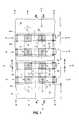
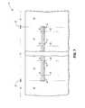
- FIG. 1is a diagrammatic, fragmented, hybrid top plan and schematic view of a substrate fragment comprising an array in accordance with an embodiment of the invention, and which comprises vertically-oriented transistors.
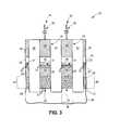
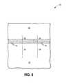
- FIG. 2is a hybrid schematic and structural cross-sectional view taken through line 2 - 2 in FIG. 1 .
- FIG. 3is a hybrid schematic and structural cross-sectional view taken through line 3 - 3 in FIG. 1 .
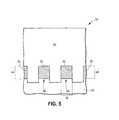
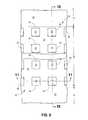
- FIG. 4is a structural cross-sectional view taken through line 4 - 4 in FIG. 1 .
- FIG. 5is a structural cross-sectional view taken through line 5 - 5 in FIG. 5 .
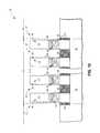
- FIG. 6is a diagrammatic top plan view of a substrate fragment in process in accordance with an embodiment of the invention.
- FIG. 7is a cross-sectional view taken through line 7 - 7 in FIG. 6 .
- FIG. 8is a cross-sectional view taken through line 8 - 8 in FIG. 6 .
- FIG. 9is a view of the FIG. 6 substrate fragment at a processing step subsequent to that shown by FIG. 6 .
- FIG. 10is a cross-sectional view taken through line 10 - 10 in FIG. 9 .
- FIG. 11is a cross-sectional view taken through line 11 - 11 in FIG. 9 .
- FIG. 12is a view of the FIG. 10 substrate fragment at a processing step subsequent to that shown by FIG. 10 , and corresponds in processing sequence to that of FIG. 13 .
- FIG. 13is a view of the FIG. 11 substrate fragment at a processing step subsequent to that shown by FIG. 11 , and corresponds in processing sequence to that of FIG. 12 .
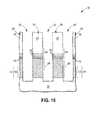
- FIG. 14is a view of the FIG. 12 substrate fragment at a processing step subsequent to that shown by FIG. 12 , and corresponds in processing sequence to that of FIG. 15 .
- FIG. 15is a view of the FIG. 13 substrate fragment at a processing step subsequent to that shown by FIG. 13 , and corresponds in processing sequence to that of FIG. 14 .
- FIG. 16is a view of an alternate embodiment substrate fragment, and corresponds in position to the cross-section of the FIG. 14 substrate fragment.
- FIG. 17is a view of the FIG. 16 substrate fragment, and corresponds in position to the cross-section of the FIG. 15 substrate fragment.
- FIG. 18is a view of a predecessor substrate fragment to that of FIG. 16 .
- FIG. 19is a view of the predecessor substrate fragment positionally corresponding to the FIG. 17 cut.
- Structure embodiments of the inventioninclude n-type field effect transistors and arrays comprising vertically-oriented transistors.
- Example embodimentsare initially described with reference to FIGS. 1-5 .
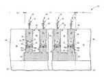
- Suchshow a substrate fragment 10 , for example a semiconductor substrate, comprising an array or sub-array area 12 and circuitry area 14 peripheral to array/sub-array area 12 .
- Array 12includes an array of vertically-oriented transistors 16 .
- verticalis a direction generally orthogonal to a primary surface relative to which the substrate is processed during fabrication and which may be considered to define a generally horizontal direction.
- vertical and “horizontal” as used hereinare generally perpendicular directions relative one another independent of orientation of the substrate in three-dimensional space.
- Circuitrymay be fabricated outside of array 12 (e.g., in area 14 ) for operating vertically-oriented transistors 16 .
- Control and/or other peripheral circuitry for operating vertically-oriented transistors 16may or may not wholly or partially be received within array 12 , with an example array as a minimum encompassing all of the vertically-oriented transistors (e.g., which may include memory cells) of a given array/sub-array.
- multiple sub-arraysmay also be fabricated and operated independently, in tandem, or otherwise relative one another.
- a “sub-array”may also be considered as an array.
- the arraycomprises memory, for example comprising a plurality of individual memory cells which include a generally vertically-oriented transistor.
- memoryfor example is DRAM, although other existing or yet-to-be-developed volatile and non-volatile memory is contemplated.
- FIGS. 1-5by way of example show array 12 as comprising a plurality of memory cells 18 which individually include a transistor 16 and a charge storage device 15 (shown schematically in FIGS. 2 and 3 ).
- Charge storage device 15is shown as being a capacitor, although other storage devices or techniques may be used and which may be formed within and/or above substrate fragment 10 .
- Substrate fragment 10comprises substrate material 22 which may be homogenous or non-homogenous, and may comprise multiple different composition materials, regions, and/or layers.
- Example materialsinclude semiconductor material, for example bulk monocrystalline silicon lightly background doped with a p-type conductivity-modifying impurity. Other semiconductor materials, including semiconductor-on-insulator substrates, may also be used.
- vertically-oriented transistors 16are field-effect transistors.
- FIGS. 1-3show individual transistors 16 as including semiconductor-comprising pedestals 24 having an elevationally outer source/drain region 30 , an elevationally inner source/drain region 28 , and a channel region 26 received elevationally between inner source/drain region 28 and outer source/drain region 30 .
- Eachmay be homogenous or non-homogenous, with suitably doped semiconductor material (e.g., monocrystalline silicon) being examples.
- inner and outer source/drain regions 28 , 30may comprise highest-doped concentration portions which are suitably conductively-doped with one type of conductivity-modifying impurity, wherein channel region 26 may be doped with a lower concentration of an opposite type impurity.
- Each region 28 and/or 30may include one or more of same-type lightly doped regions (e.g., LDD) and of opposite-type doped halo regions (neither of which is specifically designated nor shown). Regardless, individual charge storage devices 15 may electrically couple to respective outer source/drain regions 30 .
- Inner source/drain regions 28may be considered as having opposing laterally outer sides 32 ( FIG. 3 ). Further, channel regions 26 may be considered as having opposing laterally outer sides 34 ( FIG. 2 ), and in one embodiment which are transversely oriented relative to sides 32 of inner source/drain regions 28 .
- Array 12includes rows 36 of access lines and columns 38 of data/sense lines ( FIG. 1 ).
- Use of “rows” and “columns” in this documentis for convenience in distinguishing a series of access lines from a series of data/sense lines. Accordingly, “rows” and “columns” are intended to be synonymous with a series of access lines and a series of data/sense lines, respectively.
- the rowsmay be straight and/or curved and/or parallel and/or unparallel relative one another, as may be the columns. Further, the rows and columns may intersect relative one another at 90° or at one or more other angles. In the depicted example, each of the rows and columns are shown as being individually straight and angling relative one another at 90°.
- FIGS. 1-4show individual rows 36 as comprising a pair of access lines 40 a , 40 b .
- the access linesalso form gates for individual field effect transistors, and therefore in some embodiments comprise access gate lines.
- One of the pair of access lines 40 a , 40 bis operatively laterally over one of laterally outer sides 34 of channel region 26 , with the other of the pair of gate lines 40 a , 40 b being operatively laterally over the other of laterally outer sides 34 of channel region 26 .
- a gate dielectric 42is provided laterally between individual access gate lines 40 a , 40 b and respective channel regions 26 .
- Access lines 40 a , 40 bmay be homogenous or non-homogenous, may be of the same composition or of different compositions relative one another, and will comprise any suitably conductive material(s), for example any one or more of elemental metals, an alloy of elemental metals, a conductive metal compound, and conductively-doped semiconductor material(s).
- Access lines 40 a , 40 bare shown to be rectangular in cross section, although any shape may be used. Further, each need not be of the same shape relative the other.
- Access lines 40 a , 40 b and gate dielectric 42are shown as being laterally recessed relative to laterally outermost sides of source/drain regions 28 , 30 .
- access lines 40 a , 40 b and gate dielectric 42may be received laterally outward of the sides of source/drain regions 28 , 30 , for example which might simplify fabrication and/or be used to impact operation of transistors 16 .
- Access lines 40 a , 40 b within individual rows 36may be electrically coupled relative one another, for example as shown schematically via respective interconnects 41 ( FIG. 1 ).
- gate dielectricmay be received circumferentially about the channel regions (not shown), with the access line in a single row encircling that gate dielectric and running continuously as a single access line in the individual rows (not shown).
- Individual columnscomprise an inner data/sense line elevationally inward of the access lines and which interconnects transistors in that column.
- One data/sense line or multiple data/sense linesmay be used elevationally inward of the access lines for interconnecting transistors in that column.
- FIGS. 1-5show individual columns 38 as comprising a data/sense line 44 elevationally inward of access lines 40 a , 40 b .
- the elevationally inner source/drain regions 28are continuously connected in individual columns 38 to comprise at least part of the data/sense line 44 in that column ( FIG. 2 ).
- At least inner/source drain regions 28are conductively doped n-type with at least one of As and P.
- Data/sense lines 44comprise silicon-comprising semiconductor material between the transistors in that column that is conductively-doped n-type (e.g., with at least one of As and P). Ideally, source/drain regions 28 at least where connected with data/sense lines 44 are of the same composition as data/sense lines 44 and may thereby comprise a portion thereof.
- the As and/or P dopingis indicated in the figures with stippling.
- Example total As and/or P n-type dopant concentration for the highest conductive portions of inner source source/drain regions 28 and data/sense lines 44is at least 5 ⁇ 10 19 atoms/cm 3 .
- Example p-type dopant concentration for channel region 26is about 1 ⁇ 10 18 atoms/cm 3 .
- Data/sense lines 44may individually include one or more additional conductive lines (not shown), for example which may be formed of material of greater conductivity than the conductively-doped silicon-comprising material of lines 44 .
- one or more metal linesmay be formed against opposing laterally outer sides 32 of inner source/drain regions 28 .
- Example materials for such linesinclude those described above for access lines 40 a , 40 b .
- the data/sense linesmay only include one or more such metal lines wherein conductively-doped semiconductor material is not received between adjacent inner source/drain regions 28 .
- individual columnsmay comprise one or more outer data/sense lines (not shown) elevationally outward of the access lines and which electrically couple(s) to the inner date/sense line in that column, for example as disclosed in U.S. patent application Ser. No. 13/413,402 filed on Mar. 6, 2012 (now U.S. Patent Publication No. 2013/0235642), naming Lars P. Heineck and Jonathan T. Doebler as inventors, and entitled “Arrays Of Vertically-Oriented Transistors, Memory Arrays Including Vertically-Oriented Transistors, And Memory Cells”.
- Such constructionsmay lower the overall resistance of the data/sense lines to sense amplifiers external of the array. Additionally, such constructions may lower the ratio of data/sense line-to-data/sense line capacitance to data/sense line-to-world capacitance, thus perhaps improving the final signal delivered to individual sense amplifiers.
- Dielectric material 50is received about transistors 16 , including access lines 40 a , 40 b , data/sense lines 44 , and semiconductor-comprising pedestals 24 .
- Dielectric material 50may be homogenous or non-homogenous, with silicon nitride and boron and/or phosphorous doped silicon dioxide being examples.
- Access gate lines 40 a , 40 bare shown with diagonal hatching for distinguishing clarity in FIG. 1 , although such are received within dielectric material 50 as shown in FIGS. 2-4 .
- Semiconductor-comprising pedestals 24 and data/sense lines 44are diagrammatically shown as having vertical, straight, and aligned sidewalls. However, such may not be so-provided and may for example include arcuate and/or angled portions which may or may not align.
- Silicon-comprising semiconductor material 22comprises a conductivity-neutral dopant in at least one of channel region 26 and inner source/drain 28 .
- a “conductivity-neutral dopant”is conductivity-neutral to semiconductor properties in silicon and provided at a concentration that is insufficient to appreciably form a stoichiometric compound with silicon if such dopant is even capable of forming a stoichiometric compound with silicon.
- the conductivity-neutral dopantis at a concentration of about 1 ⁇ 10 19 atoms/cm 3 to about 1 ⁇ 10 22 atoms/cm 3 where received in the silicon-comprising semiconductor material.
- the conductivity-neutral dopantis provided to be substantially horizontally homogenous where received in the channel region and/or inner source/drain region.
- Example conductivity-neutral dopantsinclude N, O, S, and C. Regardless, the conductivity-neutral dopant may have no function in operation in the final circuitry construction of the transistors. However, conductivity-neutral dopants will have required attributes in method embodiments as described below.
- the n-type dopantcomprises P and the conductivity-neutral dopant comprises N. In one embodiment, the n-type dopant comprises P and the conductivity-neutral dopant comprises C.
- the conductivity-neutral dopantis provided in the inner source/drain region, and in one embodiment only in the inner source/drain region. Regardless, when so-provided the conductivity-neutral dopant may be provided in all or less than all of the inner source/drain region. In one embodiment, the conductivity-neutral dopant is provided in the channel region, and in one embodiment only in the channel region. Regardless, when so-provided the conductivity-neutral dopant may be provided in all or less than all of the channel region.
- the conductivity-neutral dopantis provided both in the channel region and in the inner source/drain region. In one embodiment when so provided, the conductivity-neutral dopant may be provided across an interface of the channel region and the inner source/drain region.
- FIGS. 2 and 3show conductivity-neutral dopant 75 provided across an interface 31 of channel region 26 and inner source/drain region 28 .
- Conductivity-neutral dopant 21may also be provided across an interface of channel region 26 and outer source/drain region 30 (not shown), or otherwise with respect to outer source/drain region 30 as described above with respect to inner source/drain region 28 .
- Embodiments of the inventionalso include an n-type field effect transistor regardless of orientation.
- a transistorincludes silicon-comprising semiconductor material which comprises a pair of source/drain regions having a channel region there-between. At least one of the source/drain regions is conductively doped n-type with at least one of As and P.
- the silicon-comprising semiconductor materialcomprises a conductivity-neutral dopant in at least one of the channel region and the at least one source/drain. Such conductivity-neutral dopant is as described above.
- a gate constructionis provided operatively proximate the channel region.
- Such an n-type field effect transistormay have any of the other constructional attributes described above in connection with the FIGS. 1-5 embodiments.
- Structures in accordance with embodiments of the inventionmay be fabricated using any existing or yet-to-be-developed techniques. For example, processing may occur at least in part as described in any one or more of U.S. patent application Ser. No. 12/917,346 filed on Nov. 1, 2010 (now U.S. Pat. No. 8,361,856), naming Lars P. Heineck and Jaydip Guha as inventors, and entitled “Memory Cells, Arrays Of Memory Cells, And Methods Of Forming Memory Cells”; U.S. patent application Ser. No. 13/031,829 filed on Feb. 22, 2011 (now U.S. Pat. No. 8,450,175), naming Jaydip Guha, Shyam Surthi, Suraj J.
- embodiments of the inventioninclude methods of forming an array comprising vertically-oriented transistors. Additionally, embodiments of the invention include methods of forming an n-type field effect transistor of any orientation. Further, aspects of the structure embodiments are not limited by the method embodiments, or vice versa.
- FIGS. 6-15Example method embodiments of the invention are next described with reference to FIGS. 6-15 , for example in fabricating the largely finished-construction circuitry of FIGS. 1-5 . Accordingly, like numerals from FIGS. 1-5 for the same components or materials are also used in FIGS. 6-15 .
- FIGS. 6-8show a predecessor substrate fragment 10 that includes silicon-comprising semiconductor material 22 . Array 12 and peripheral regions 14 are shown, although such may not yet be distinguishable relative the other.
- Conductivity-neutral dopant 75has been ion implanted into silicon-comprising semiconductor material in at least one of a location of the channel region and a location of the inner source/drain region of individual of the vertically-oriented transistors being formed.
- FIGS. 6-8show conductivity-neutral dopant 75 as being within both of channel region locations 26 and inner source/drain locations 28 for fabrication of the example construction of FIGS. 1-5 .
- conductivity-neutral dopant in accordance with method embodimentsis selected to restrict diffusion of the at least one of As and P in silicon-comprising semiconductor material 22 from inner source/drain region location 28 to channel region location 26 under a set of heating conditions than would otherwise occur under the set of heating conditions in the absence of the conductivity-neutral dopant.
- Examplesinclude N, O, and S for each of As and P, with N of such group being ideal.
- the conductivity-neutral dopantmay comprise C. The artisan can select suitable implant energy and dose to achieve desired depth, elevational spread, and resultant concentration of the implant specie/species.
- the conductivity-neutral dopantis ion implanted blanketly across a single continuous horizontal area of the silicon-comprising semiconductor material, for example the horizontal area that would be bounded between lines 27 ( FIGS. 6 and 7 ).
- FIGS. 6-8also show an example embodiment wherein the conductivity-neutral dopant has not largely been provided throughout peripheral region 14 . Alternately, such may be so provided, for example in either patterned or blanket manners.
- the conductivity-neutral dopantis provided to be substantially horizontally homogenous where received in the silicon-comprising semiconductor material.
- An example thickness range for the region comprising conductivity-neutral dopantis from about 50 Angstroms to about 2,000 Angstroms.
- Example conductivity-neutral dopant concentrationsare as described above with respect to dopant 75 in the example finished-circuitry construction of FIGS. 1-5 .
- opening/openings 37have been formed through silicon-comprising semiconductor material 22 .
- An upper portion of individual locations 28are shown as having been doped n-type, for example to constitute lightly-doped drain (LDD) regions.
- LDDlightly-doped drain
- an example techniqueis by ion implantation, and which may occur earlier or later in the process than shown by FIGS. 10 and 11 .
- LDD implantmay be conducted into material 22 before or after etching to form some or all of opening/openings 37 .
- LDD regionsmay be formed in whole or in part by out-diffusion of As and/or P that has been provided in areas remote from the upper portions of locations 28 , as will be described below.
- FIGS. 9-11show semiconductor-comprising pedestals 24 have been partially formed whereby openings 37 appear as a single continuous opening in FIG. 9 .
- only parallel trenchesmay be etched into material 22 at this point in the process.
- parallel trenchesmay be etched into silicon-comprising semiconductor material 22 between columns 38 in FIG. 1 , thereby forming rails (not shown) of silicon-comprising semiconductor material 22 between such trenches.
- those trenchesmay initially only be etched into material 22 to have bases that are proximate the uppermost portions of locations 28 , and perhaps followed by an LDD and/or halo implant.
- those trenchescould be etched deeper to the depth shown in FIGS. 9 and 11 .
- such trenchescould be initially etched to the depth shown regardless of when or if LDD and/or halo regions are ever formed.
- trenches orthogonal theretomay be etched to form pedestals 24 .
- pedestals 24 as shown in FIGS. 9-11may not be formed at this point in the process. Accordingly and regardless, opening/openings 37 and/or trenches may be formed in one or more etching and/or masking steps.
- Semiconductor-comprising pedestals 24 in FIGS. 9-11are diagrammatically shown as having vertical, straight, and aligned sidewalls. However, such may not be so-provided and may for example include arcuate and/or angled portions regardless of any alignment. Further, silicon-comprising semiconductor material 22 of the pedestals or trenches may be lined with one or more dielectric materials during processing (not shown), and which may comprise a portion of dielectric 50 in the finished-circuitry construction.
- FIGS. 10 and 11show ion implanting having been conducted of at least one n-type impurity into an elevational region 23 laterally adjacent locations 28 where inner source/drain regions will be formed (shown by darker stippling).
- opening/openings 37are formed in two separate orthogonal trench masking steps as described above, the conductively-doped n-type regions may solely extend in parallel lines at this point in the process, for example along lines between column lines 38 of FIG. 1 (not shown in FIGS. 10 and 11 ). Regardless, that n-type dopant impurity will ultimately diffuse into adjacent locations 28 .
- the n-type dopant provided in the implanted regionsis provided at a concentration that is sufficient to ultimately render the silicon-comprising semiconductor material within which the dopant is received electrically conductive, and to render at least the lowest-most portions of regions 28 electrically conductive after the n-type dopant diffuses therein. Regardless, at least one of As and P are ultimately provided into the silicon-comprising semiconductor material in the inner source/drain regions locations to at least partially form the inner source/drain regions.
- the silicon-comprising semiconductor material 22 within which conductivity-neutral dopant 75 is receivedhas been subjected to the set of heating conditions.
- the conductivity-neutral dopantrestricts diffusion of the As and/or P in the silicon-comprising semiconductor material from inner source/drain region locations 28 to channel region locations 26 than would otherwise occur under the set of heating conditions in the absence of the conductivity-neutral dopant.
- Example conditionsinclude subjecting the substrate to 900° C. for about 30 minutes in an inert atmosphere.
- the set of conditionsis sufficient to act as a dopant activation anneal for activating the As, P, and/or other n-type dopant(s).
- the set of conditionsmay be used to diffuse As, P, and/or other n-type dopant(s) in forming LDD regions proximate channel regions 26 as part of inner source/drain regions 28 particularly where such are not provided separately by ion implantation or other manner. Precluding, or at least reducing, As and/or P diffusion from inner source/drain regions 28 into channel regions 26 may improve access device sub-threshold slope.
- the set of heating conditionsmay interconnect the laterally-spaced conductively-doped n-type regions (as shown in FIGS. 10 and 11 ) within region 23 as is shown in FIGS. 12 and 13 .
- forming the data/sense linesincludes etching deeper into silicon-comprising semiconductor material 22 , and in one embodiment etching through region 23 . For example as shown in FIGS. 14 and 15 , region 23 has been etched through to form data/sense lines 44 .
- silicon-comprising material 22might be etched first to form the lines (not shown) and then the substrate subjected to the set of heating conditions to interconnect laterally-spaced conductively-doped n-type regions.
- data/sense linesmay be formed that only include one or more buried metal lines (not shown) wherein conductively-doped semiconductor material is not received between adjacent inner source/drain regions 28 .
- pedestals 24may be so formed by etching orthogonally oriented parallel trenches after the example FIGS. 14 and 15 etching has been conducted.
- Processingmay continue in forming a structure as shown and described relative to FIGS. 1-5 , or otherwise, and is not germane to invention herein.
- Conductivity-neutral dopantmay be provided within the silicon-comprising semiconductor material using techniques other than ion implantation in the above and other embodiments. Further and regardless, the FIGS. 6-15 processing shows formation of conductivity-neutral dopant within the silicon-comprising semiconductor material before the n-type dopant is so provided. This relationship may be reversed whereby the n-type dopant which comprises part of the inner source/drain regions is formed in the silicon-comprising semiconductor material before the conductivity-neutral dopant is provided in the silicon-comprising semiconductor material.
- FIGS. 16 and 17show example additional processing having been conducted with respect to the FIGS. 14 and 15 substrate either prior to or thereafter, but regardless prior to subjecting the silicon-comprising semiconductor material to the set of heating conditions as shown by FIGS. 12 and 13 .
- conductivity-neutral dopant 75has also been provided into silicon-comprising semiconductor material 22 that is immediately elevationally inward of location of region 23 .
- Such conductivity-neutral dopant 75has the same attributes as described in the above method embodiments regarding restricting diffusion of at least one of As and P in silicon-comprising semiconductor material, although may not necessarily be the same composition dopant(s). Providing a region of silicon-comprising semiconductor material containing at least one of As and P that is bounded on different sides (e.g., top and bottom) by conductivity-neutral dopant 75 would restrict diffusion of As and/or P in two different (e.g., opposite) directions.
- FIGS. 18 and 19show but one example processing of a predecessor substrate fragment 10 a to that of FIGS. 16 and 17 , respectively.
- FIGS. 18 and 19correspond in processing sequence to that of FIGS. 7 and 8 , and show conductivity-neutral dopant 75 having also been provided into silicon-comprising semiconductor material 22 that is immediately elevationally inward of location of region 23 prior to providing at least one of As and P into the silicon-comprising semiconductor material in inner source/drain region locations 28 .
- Embodiments of the inventionalso include a method of forming an n-type field effect transistor independent of whether fabricated in connection with formation of vertically-oriented transistors, and even if so independent of the above described structures.
- Such a methodincludes providing a conductivity-neutral dopant in silicon-comprising semiconductor material in at least one of a channel region location and a first source/drain region location of a field effect transistor being formed.
- N-type dopantis provided in the silicon-comprising semiconductor material in a second source/drain region location and in the first source/drain region location.
- the n-type dopant at least in the first source/drain region locationcomprises at least one of As and P.
- the silicon-comprising semiconductor materialis subjected to a set of heating conditions.
- the conductivity-neutral dopantrestricts diffusion of the As and/or P in the silicon-comprising semiconductor material from the first source/drain region location to the channel region location than would otherwise occur under the set of heating conditions in the absence of the conductivity-neutral dopant.
- a channel regionis ultimately formed, as is a gate construction operatively proximate the channel region.
- One or both of the providing of the n-type and conductivity-neutral dopantsmay occur by ion implantation or other technique and/or otherwise as described above. Further either may be provided within the silicon-comprising semiconductor material before or after the other. Any other attribute as described above may be used in such methods of forming transistors.
- a method of forming an n-type field effect transistorcomprises providing a conductivity-neutral dopant in silicon-comprising semiconductor material in at least one of a channel region location and a first source/drain region location of a field effect transistor being formed.
- N-type dopantis provided in the silicon-comprising semiconductor material in a second source/drain region location and in the first source/drain region location.
- the n-type dopant at least in the first source/drain region locationcomprises at least one of As and P.
- the silicon-comprising semiconductor materialis subjected to a set of heating conditions.
- the conductivity-neutral dopantrestricts diffusion of the at least one of As and P in the silicon-comprising semiconductor material from the first source/drain region location to the channel region location than would otherwise occur under the set of heating conditions in the absence of the conductivity-neutral dopant.
- a channel regionis formed and a gate construction is formed operatively proximate the channel region.
- a methodincludes forming an array comprising vertically-oriented n-type transistors.
- the transistorsindividually comprise an elevationally outer source/drain region, an elevationally inner source/drain region comprising silicon-comprising semiconductor material that is conductively-doped n-type with at least one of As and P, and a silicon-comprising semiconductor material channel region elevationally between the inner and outer source/drain regions.
- a conductivity-neutral dopantis ion implanted into silicon-comprising semiconductor material in at least one of a location of the channel region and a location of the inner source/drain region of individual of the vertically-oriented transistors being formed.
- At least one of As and Pis provided into the silicon-comprising semiconductor material in the inner source/drain region locations to at least partially form the inner source/drain regions.
- the silicon-comprising semiconductor materialis subjected to a set of heating conditions.
- the conductivity-neutral dopantrestricts diffusion of the at least one of As and P in the silicon-comprising semiconductor material from the inner source/drain region locations to the channel region locations than would otherwise occur under the set of heating conditions in the absence of the conductivity-neutral dopant.
- the channel regionis formed as is a gate construction operatively proximate the channel region.
- an n-type field effect transistorincludes silicon-comprising semiconductor material comprising a pair of source/drain regions having a channel region there-between. At least one of the source/drain regions is conductively doped n-type with at least one of As and P. A conductivity-neutral dopant is in the silicon-comprising semiconductor material in at least one of the channel region and the at least one source/drain region. A gate construction is operatively proximate the channel region.
- an arraycomprises n-type vertically-oriented transistors, including rows of access lines and columns of data/sense lines.
- Individual vertically-oriented transistorscomprise silicon-comprising semiconductor material comprising an elevationally outer source/drain region, an elevationally inner source/drain region, and a channel region elevationally between the inner and outer source/drain regions. At least the inner source/drain region is conductively doped n-type with at least one of As and P.
- a conductivity-neutral dopantis in the silicon-comprising semiconductor material in at least one of the channel region and the inner source/drain region.
- Individual of the rowscomprise an access line interconnecting transistors in that row.
- Individual of the columnscomprise a data/sense line interconnecting transistors in that column.
- a method of forming an array comprising vertically-oriented n-type transistorsincludes transistors individually comprising an elevationally outer source/drain region, an elevationally inner source/drain region comprising silicon-comprising semiconductor material that is conductively-doped n-type with at least one of As and P, and a silicon-comprising semiconductor material channel region elevationally between the inner and outer source/drain regions.
- Gates of the vertically-oriented transistorscomprise rows of access lines. Individual of the rows comprising an access line interconnecting transistors in that row. Columns of data/sense lines are provided. Individual of the columns comprise a data/sense line interconnecting transistors in that column.
- Individual of the data/sense linescomprise continuously running conductively As-doped and/or P-doped silicon-comprising semiconductor material.
- the methodcomprises ion implanting a conductivity-neutral dopant into silicon-comprising semiconductor material in at least one of a location of the channel region and a location of the inner source/drain region of individual of the vertically-oriented transistors being formed.
- a conductivity-neutral dopantis ion implanted into silicon-comprising semiconductor material that is immediately elevationally inward of a location of the continuously running conductively As and/or P doped silicon-comprising semiconductor material.
- At least one of As and Pis provided into the silicon-comprising semiconductor material in the inner source/drain region locations to at least partially form the inner source/drain regions.
- the silicon-comprising semiconductor materialis subjected to a set of heating conditions.
- the conductivity-neutral dopant that is in at least one of a location of the channel region and a location of the inner source/drain region of individual of the vertically-oriented transistors being formedrestricts diffusion of the at least one of As and P in the silicon-comprising semiconductor material from the inner source/drain region locations to the channel region locations than would otherwise occur under the set of heating conditions in the absence of the conductivity-neutral dopant.
- the conductivity-neutral dopant that is in said immediately elevationally inward silicon-comprising semiconductor materialrestricting diffusion of the at least one of As and P in the continuously running conductively As and/or P doped silicon-comprising semiconductor material, into said immediately elevationally inward silicon-comprising semiconductor material than would otherwise occur under the set of heating conditions in the absence of the conductivity-neutral dopant in said immediately elevationally inward silicon-comprising semiconductor material.
- the channel regionis formed, as is a gate construction operatively proximate the channel region.
Landscapes
- Physics & Mathematics (AREA)
- High Energy & Nuclear Physics (AREA)
- Engineering & Computer Science (AREA)
- Health & Medical Sciences (AREA)
- Toxicology (AREA)
- Condensed Matter Physics & Semiconductors (AREA)
- General Physics & Mathematics (AREA)
- Manufacturing & Machinery (AREA)
- Computer Hardware Design (AREA)
- Microelectronics & Electronic Packaging (AREA)
- Power Engineering (AREA)
- Insulated Gate Type Field-Effect Transistor (AREA)
Abstract
Description
Claims (32)
Priority Applications (2)
| Application Number | Priority Date | Filing Date | Title |
|---|---|---|---|
| US13/591,073US9006060B2 (en) | 2012-08-21 | 2012-08-21 | N-type field effect transistors, arrays comprising N-type vertically-oriented transistors, methods of forming an N-type field effect transistor, and methods of forming an array comprising vertically-oriented N-type transistors |
| US14/679,703US9472663B2 (en) | 2012-08-21 | 2015-04-06 | N-type field effect transistors, arrays comprising N-type vertically-oriented transistors, methods of forming an N-type field effect transistor, and methods of forming an array comprising vertically-oriented N-type transistors |
Applications Claiming Priority (1)
| Application Number | Priority Date | Filing Date | Title |
|---|---|---|---|
| US13/591,073US9006060B2 (en) | 2012-08-21 | 2012-08-21 | N-type field effect transistors, arrays comprising N-type vertically-oriented transistors, methods of forming an N-type field effect transistor, and methods of forming an array comprising vertically-oriented N-type transistors |
Related Child Applications (1)
| Application Number | Title | Priority Date | Filing Date |
|---|---|---|---|
| US14/679,703DivisionUS9472663B2 (en) | 2012-08-21 | 2015-04-06 | N-type field effect transistors, arrays comprising N-type vertically-oriented transistors, methods of forming an N-type field effect transistor, and methods of forming an array comprising vertically-oriented N-type transistors |
Publications (2)
| Publication Number | Publication Date |
|---|---|
| US20140054678A1 US20140054678A1 (en) | 2014-02-27 |
| US9006060B2true US9006060B2 (en) | 2015-04-14 |
Family
ID=50147243
Family Applications (2)
| Application Number | Title | Priority Date | Filing Date |
|---|---|---|---|
| US13/591,073Active2033-01-11US9006060B2 (en) | 2012-08-21 | 2012-08-21 | N-type field effect transistors, arrays comprising N-type vertically-oriented transistors, methods of forming an N-type field effect transistor, and methods of forming an array comprising vertically-oriented N-type transistors |
| US14/679,703ActiveUS9472663B2 (en) | 2012-08-21 | 2015-04-06 | N-type field effect transistors, arrays comprising N-type vertically-oriented transistors, methods of forming an N-type field effect transistor, and methods of forming an array comprising vertically-oriented N-type transistors |
Family Applications After (1)
| Application Number | Title | Priority Date | Filing Date |
|---|---|---|---|
| US14/679,703ActiveUS9472663B2 (en) | 2012-08-21 | 2015-04-06 | N-type field effect transistors, arrays comprising N-type vertically-oriented transistors, methods of forming an N-type field effect transistor, and methods of forming an array comprising vertically-oriented N-type transistors |
Country Status (1)
| Country | Link |
|---|---|
| US (2) | US9006060B2 (en) |
Families Citing this family (9)
| Publication number | Priority date | Publication date | Assignee | Title |
|---|---|---|---|---|
| US10014305B2 (en) | 2016-11-01 | 2018-07-03 | Micron Technology, Inc. | Methods of forming an array comprising pairs of vertically opposed capacitors and arrays comprising pairs of vertically opposed capacitors |
| US9761580B1 (en) | 2016-11-01 | 2017-09-12 | Micron Technology, Inc. | Methods of forming an array comprising pairs of vertically opposed capacitors and arrays comprising pairs of vertically opposed capacitors |
| US10062745B2 (en) | 2017-01-09 | 2018-08-28 | Micron Technology, Inc. | Methods of forming an array of capacitors, methods of forming an array of memory cells individually comprising a capacitor and a transistor, arrays of capacitors, and arrays of memory cells individually comprising a capacitor and a transistor |
| US9837420B1 (en) | 2017-01-10 | 2017-12-05 | Micron Technology, Inc. | Arrays of memory cells individually comprising a capacitor and an elevationally-extending transistor, methods of forming a tier of an array of memory cells, and methods of forming an array of memory cells individually comprising a capacitor and an elevationally-extending transistor |
| US9935114B1 (en) | 2017-01-10 | 2018-04-03 | Micron Technology, Inc. | Methods of forming an array comprising pairs of vertically opposed capacitors and arrays comprising pairs of vertically opposed capacitors |
| US9842839B1 (en) | 2017-01-12 | 2017-12-12 | Micron Technology, Inc. | Memory cell, an array of memory cells individually comprising a capacitor and a transistor with the array comprising rows of access lines and columns of digit lines, a 2T-1C memory cell, and methods of forming an array of capacitors and access transistors there-above |
| US10388658B1 (en) | 2018-04-27 | 2019-08-20 | Micron Technology, Inc. | Transistors, arrays of transistors, arrays of memory cells individually comprising a capacitor and an elevationally-extending transistor, and methods of forming an array of transistors |
| US11348932B2 (en)* | 2019-03-06 | 2022-05-31 | Micron Technology, Inc. | Integrated assemblies having transistor body regions coupled to carrier-sink-structures; and methods of forming integrated assemblies |
| US11038027B2 (en)* | 2019-03-06 | 2021-06-15 | Micron Technology, Inc. | Integrated assemblies having polycrystalline first semiconductor material adjacent conductively-doped second semiconductor material |
Citations (76)
| Publication number | Priority date | Publication date | Assignee | Title |
|---|---|---|---|---|
| US3562022A (en) | 1967-12-26 | 1971-02-09 | Hughes Aircraft Co | Method of doping semiconductor bodies by indirection implantation |
| US3865624A (en) | 1970-06-29 | 1975-02-11 | Bell Telephone Labor Inc | Interconnection of electrical devices |
| US4673962A (en) | 1985-03-21 | 1987-06-16 | Texas Instruments Incorporated | Vertical DRAM cell and method |
| US4764394A (en) | 1987-01-20 | 1988-08-16 | Wisconsin Alumni Research Foundation | Method and apparatus for plasma source ion implantation |
| US4920390A (en) | 1985-07-02 | 1990-04-24 | Matsushita Electric Industrial Co., Ltd. | Semiconductor memory device and method of fabricating the same |
| US5374456A (en) | 1992-12-23 | 1994-12-20 | Hughes Aircraft Company | Surface potential control in plasma processing of materials |
| US5508212A (en) | 1995-04-27 | 1996-04-16 | Taiwan Semiconductor Manufacturing Co. | Salicide process for a MOS semiconductor device using nitrogen implant of titanium |
| US5627390A (en) | 1994-05-26 | 1997-05-06 | Mitsubishi Denki Kabushiki Kaisha | Semiconductor device with columns |
| US5672541A (en) | 1995-06-14 | 1997-09-30 | Wisconsin Alumni Research Foundation | Ultra-shallow junction semiconductor device fabrication |
| US5828094A (en) | 1994-03-17 | 1998-10-27 | Samsung Electronics Co., Ltd. | Memory cell structure having a vertically arranged transistors and capacitors |
| US5897363A (en) | 1996-05-29 | 1999-04-27 | Micron Technology, Inc. | Shallow junction formation using multiple implant sources |
| US6137713A (en) | 1998-10-20 | 2000-10-24 | Matsushita Electric Industrial Co., Ltd. | Semiconductor storage device |
| US6221724B1 (en)* | 1998-11-06 | 2001-04-24 | Advanced Micro Devices, Inc. | Method of fabricating an integrated circuit having punch-through suppression |
| US6225151B1 (en) | 1997-06-09 | 2001-05-01 | Advanced Micro Devices, Inc. | Nitrogen liner beneath transistor source/drain regions to retard dopant diffusion |
| US6329686B1 (en) | 1999-11-12 | 2001-12-11 | Micron Technology, Inc. | Method of fabricating conductive straps to interconnect contacts to corresponding digit lines by employing an angled sidewall implant and semiconductor devices fabricated thereby |
| US6417040B2 (en) | 1997-04-25 | 2002-07-09 | Micron Technology, Inc. | Method for forming memory array having a digit line buried in an isolation region |
| US20020110039A1 (en) | 2001-02-09 | 2002-08-15 | Micron Technology, Inc. | Memory address and decode circuits with ultra thin body transistors |
| US6492245B1 (en) | 2001-10-16 | 2002-12-10 | Taiwan Semiconductor Manufacturing Company | Method of forming air gap isolation between a bit line contact structure and a capacitor under bit line structure |
| US6504201B1 (en) | 1997-07-08 | 2003-01-07 | Micron Technology, Inc. | Memory cell having a vertical transistor with buried source/drain and dual gates |
| US6563162B2 (en) | 2001-03-21 | 2003-05-13 | Samsung Electronics Co., Ltd. | Semiconductor memory device for reducing parasitic bit line capacitance and method of fabricating the same |
| US20030096490A1 (en) | 2001-11-16 | 2003-05-22 | John Borland | Method of forming ultra shallow junctions |
| US20030107911A1 (en) | 2001-12-12 | 2003-06-12 | Ryuji Nishihara | Semiconductor memory device |
| US6582998B2 (en) | 2000-04-21 | 2003-06-24 | Matsushita Electric Industrial Co., Ltd. | Method for fabricating nonvolatile semiconductor memory device |
| US6593612B2 (en) | 2000-12-05 | 2003-07-15 | Infineon Technologies Ag | Structure and method for forming a body contact for vertical transistor cells |
| US20030186519A1 (en) | 2002-04-01 | 2003-10-02 | Downey Daniel F. | Dopant diffusion and activation control with athermal annealing |
| US6639846B2 (en) | 2001-04-02 | 2003-10-28 | Infineon Technologies Ag | Method and circuit configuration for a memory for reducing parasitic coupling capacitances |
| US6689660B1 (en) | 1997-07-08 | 2004-02-10 | Micron Technology, Inc. | 4 F2 folded bit line DRAM cell structure having buried bit and word lines |
| US6716727B2 (en) | 2001-10-26 | 2004-04-06 | Varian Semiconductor Equipment Associates, Inc. | Methods and apparatus for plasma doping and ion implantation in an integrated processing system |
| KR20040055142A (en) | 2002-12-20 | 2004-06-26 | 주식회사 하이닉스반도체 | Structure of DRAM cell array |
| US20040132232A1 (en) | 1998-02-24 | 2004-07-08 | Micron Technology, Inc. | Vertical gain cell and array for a dynamic random access memory and method for forming the same |
| US20040195594A1 (en) | 1997-04-22 | 2004-10-07 | Micron Technology, Inc. | Method of forming integrated circuitry |
| US20050017281A1 (en) | 1999-09-02 | 2005-01-27 | Lowrey Tyler A. | Methods of fabricating buried digit lines and semiconductor devices including same |
| US20050079721A1 (en) | 1994-08-15 | 2005-04-14 | Buerger Walter Richard | Vertically wired integrated circuit and method of fabrication |
| US20050260838A1 (en) | 2002-05-10 | 2005-11-24 | Varian Semiconductor Equipment Associates, Inc. | Methods and systems for dopant profiling |
| US6977417B2 (en)* | 2002-06-24 | 2005-12-20 | Fujitsu Limited | Semiconductor device and method of fabricating the same |
| US20060017088A1 (en) | 2004-07-20 | 2006-01-26 | Abbott Todd R | DRAM layout with vertical FETS and method of formation |
| US6992349B2 (en) | 2000-08-14 | 2006-01-31 | Matrix Semiconductor, Inc. | Rail stack array of charge storage devices and method of making same |
| US20060059449A1 (en) | 2004-09-15 | 2006-03-16 | Samsung Electronics Co., Ltd. | Line layout structure of semiconductor memory devices |
| US7015091B1 (en) | 2004-11-18 | 2006-03-21 | Promos Technologies, Inc. | Integration of silicon carbide into DRAM cell to improve retention characteristics |
| US20060081884A1 (en) | 2004-03-11 | 2006-04-20 | Micron Technology, Inc. | Semiconductor constructions |
| US7052941B2 (en) | 2003-06-24 | 2006-05-30 | Sang-Yun Lee | Method for making a three-dimensional integrated circuit structure |
| US7074656B2 (en) | 2003-04-29 | 2006-07-11 | Taiwan Semiconductor Manufacturing Company, Ltd. | Doping of semiconductor fin devices |
| US7099174B2 (en) | 2001-03-15 | 2006-08-29 | Micron Technology, Inc. | Metal wiring pattern for memory devices |
| US20060249770A1 (en) | 2005-05-03 | 2006-11-09 | Samsung Electronics Co., Ltd. | Single Transistor Floating-Body DRAM Devices Having Vertical Channel Transistor Structures and Methods of Fabricating the Same |
| US7166479B2 (en) | 1999-05-25 | 2007-01-23 | Micron Technology, Inc. | Methods of forming magnetic shielding for a thin-film memory element |
| US20070087574A1 (en) | 2005-10-13 | 2007-04-19 | Varian Semiconductor Equipment Associates, Inc. | Conformal doping apparatus and method |
| US20070171742A1 (en) | 2006-01-25 | 2007-07-26 | Yi Chul-Woo | Semiconductor memory device having an open bit line structure, and method of testing the same |
| US20070243680A1 (en) | 2006-04-13 | 2007-10-18 | Eliyahou Harari | Methods of Making Flash Memory Cell Arrays Having Dual Control Gates Per Memory Cell Charge Storage Element |
| US7365384B2 (en) | 2002-11-15 | 2008-04-29 | Micron Technology, Inc. | Trench buried bit line memory devices and methods thereof |
| US20080142931A1 (en) | 2004-03-25 | 2008-06-19 | Matsushita Electric Industrial Co., Ltd. | Method of Impurity Introduction, Impurity Introduction Apparatus and Semiconductor Device Produced with Use of the Method |
| US20080217655A1 (en) | 2007-02-10 | 2008-09-11 | Qimonda Ag | Integrated circuit with buried control line structures |
| US20080268628A1 (en) | 2007-04-25 | 2008-10-30 | Puneet Kohli | N-type semiconductor component with improved dopant implantation profile and method of forming same |
| US20080277738A1 (en) | 2007-05-08 | 2008-11-13 | Venkat Ananthan | Memory cells, memory banks, memory arrays, and electronic systems |
| US7456068B2 (en) | 2006-06-08 | 2008-11-25 | Intel Corporation | Forming ultra-shallow junctions |
| US7491641B2 (en) | 2004-08-23 | 2009-02-17 | Micron Technology, Inc. | Method of forming a conductive line and a method of forming a conductive contact adjacent to and insulated from a conductive line |
| US7501676B2 (en) | 2005-03-25 | 2009-03-10 | Micron Technology, Inc. | High density semiconductor memory |
| US20090121268A1 (en) | 2007-11-09 | 2009-05-14 | Samsung Electronics Co., Ltd. | Semiconductor Memory Devices Having Vertical Channel Transistors and Related Methods |
| US7592212B2 (en) | 2007-04-06 | 2009-09-22 | Micron Technology, Inc. | Methods for determining a dose of an impurity implanted in a semiconductor substrate |
| US20090256187A1 (en) | 2008-04-10 | 2009-10-15 | Kyung Do Kim | Semiconductor device having vertical pillar transistors and method for manufacturing the same |
| US20100038709A1 (en) | 2008-08-15 | 2010-02-18 | Nanya Technology Corporation | Vertical transistor and array with vertical transistors |
| US7713823B2 (en) | 2007-11-02 | 2010-05-11 | Hynix Semiconductor Inc. | Semiconductor device with vertical channel transistor and method for fabricating the same |
| US7737010B2 (en) | 2006-04-14 | 2010-06-15 | Micron Technology, Inc. | Method of photoresist strip for plasma doping process of semiconductor manufacturing |
| US7768073B2 (en) | 2005-01-14 | 2010-08-03 | Micron Technology, Inc. | Memory array buried digit line |
| US20100237423A1 (en) | 2006-06-09 | 2010-09-23 | Samsung Electronics Co., Ltd. | Semiconductor devices including buried bit lines |
| US20110019486A1 (en) | 2009-07-22 | 2011-01-27 | Samsung Electronics Co., Ltd. | Semiconductor memory device and programming method thereof |
| US7939409B2 (en) | 2005-09-01 | 2011-05-10 | Micron Technology, Inc. | Peripheral gate stacks and recessed array gates |
| US7948064B2 (en) | 2008-09-30 | 2011-05-24 | Infineon Technologies Ag | System on a chip with on-chip RF shield |
| US7956402B2 (en) | 2002-08-29 | 2011-06-07 | Micron Technology, Inc. | Double-doped polysilicon floating gate |
| US8008158B2 (en) | 2008-07-10 | 2011-08-30 | Taiwan Semiconductor Manufacturing Co., Ltd. | Dopant implantation method using multi-step implants |
| US20110215408A1 (en) | 2010-03-02 | 2011-09-08 | Micron Technology, Inc. | Floating body cell structures, devices including same, and methods for forming same |
| US20110215391A1 (en) | 2010-03-08 | 2011-09-08 | Elpida Memory, Inc. | Semiconductor device and method of manufacturing the same |
| US20110220994A1 (en) | 2010-03-10 | 2011-09-15 | Micron Technology, Inc. | Method of Forming a DRAM Array of Devices with Vertically Integrated Recessed Access Device and Digitline |
| US20120104491A1 (en) | 2010-11-01 | 2012-05-03 | Lars Heineck | Memory Cells, Arrays Of Memory Cells, And Methods Of Forming Memory Cells |
| US20120214285A1 (en) | 2011-02-22 | 2012-08-23 | Jaydip Guha | Methods Of Forming A Vertical Transistor And At Least A Conductive Line Electrically Coupled Therewith, Methods Of Forming Memory Cells, And Methods Of Forming Arrays Of Memory Cells |
| US20130168757A1 (en) | 2011-12-28 | 2013-07-04 | Young-Ok HONG | Nonvolatile memory device and method for fabricating the same |
| WO2014035568A1 (en) | 2012-08-27 | 2014-03-06 | Micron Technology, Inc. | Arrays of vertically-oriented transistors, and memory arrays including vertically-oriented transistors |
Family Cites Families (6)
| Publication number | Priority date | Publication date | Assignee | Title |
|---|---|---|---|---|
| US4829018A (en) | 1986-06-27 | 1989-05-09 | Wahlstrom Sven E | Multilevel integrated circuits employing fused oxide layers |
| US7012021B2 (en) | 2004-01-29 | 2006-03-14 | Taiwan Semiconductor Mfg | Method for end point detection polysilicon chemical mechanical polishing in an anti-fuse memory device |
| US7365385B2 (en) | 2004-08-30 | 2008-04-29 | Micron Technology, Inc. | DRAM layout with vertical FETs and method of formation |
| KR100725370B1 (en) | 2006-01-05 | 2007-06-07 | 삼성전자주식회사 | Method of manufacturing semiconductor device and semiconductor device manufactured thereby |
| KR100979360B1 (en) | 2008-03-13 | 2010-08-31 | 주식회사 하이닉스반도체 | Semiconductor device and manufacturing method thereof |
| KR101669261B1 (en) | 2010-06-14 | 2016-10-25 | 삼성전자주식회사 | Semiconductor device having vertical channel transistor and method for manufacturing the same |
- 2012
- 2012-08-21USUS13/591,073patent/US9006060B2/enactiveActive
- 2015
- 2015-04-06USUS14/679,703patent/US9472663B2/enactiveActive
Patent Citations (81)
| Publication number | Priority date | Publication date | Assignee | Title |
|---|---|---|---|---|
| US3562022A (en) | 1967-12-26 | 1971-02-09 | Hughes Aircraft Co | Method of doping semiconductor bodies by indirection implantation |
| US3865624A (en) | 1970-06-29 | 1975-02-11 | Bell Telephone Labor Inc | Interconnection of electrical devices |
| US4673962A (en) | 1985-03-21 | 1987-06-16 | Texas Instruments Incorporated | Vertical DRAM cell and method |
| US4920390A (en) | 1985-07-02 | 1990-04-24 | Matsushita Electric Industrial Co., Ltd. | Semiconductor memory device and method of fabricating the same |
| US4764394A (en) | 1987-01-20 | 1988-08-16 | Wisconsin Alumni Research Foundation | Method and apparatus for plasma source ion implantation |
| US5374456A (en) | 1992-12-23 | 1994-12-20 | Hughes Aircraft Company | Surface potential control in plasma processing of materials |
| US5828094A (en) | 1994-03-17 | 1998-10-27 | Samsung Electronics Co., Ltd. | Memory cell structure having a vertically arranged transistors and capacitors |
| US5627390A (en) | 1994-05-26 | 1997-05-06 | Mitsubishi Denki Kabushiki Kaisha | Semiconductor device with columns |
| US20050079721A1 (en) | 1994-08-15 | 2005-04-14 | Buerger Walter Richard | Vertically wired integrated circuit and method of fabrication |
| US5508212A (en) | 1995-04-27 | 1996-04-16 | Taiwan Semiconductor Manufacturing Co. | Salicide process for a MOS semiconductor device using nitrogen implant of titanium |
| US5672541A (en) | 1995-06-14 | 1997-09-30 | Wisconsin Alumni Research Foundation | Ultra-shallow junction semiconductor device fabrication |
| US5897363A (en) | 1996-05-29 | 1999-04-27 | Micron Technology, Inc. | Shallow junction formation using multiple implant sources |
| US7179703B2 (en) | 1996-05-29 | 2007-02-20 | Micron Technology, Inc. | Method of forming shallow doped junctions having a variable profile gradation of dopants |
| US20040195594A1 (en) | 1997-04-22 | 2004-10-07 | Micron Technology, Inc. | Method of forming integrated circuitry |
| US6417040B2 (en) | 1997-04-25 | 2002-07-09 | Micron Technology, Inc. | Method for forming memory array having a digit line buried in an isolation region |
| US6225151B1 (en) | 1997-06-09 | 2001-05-01 | Advanced Micro Devices, Inc. | Nitrogen liner beneath transistor source/drain regions to retard dopant diffusion |
| US6689660B1 (en) | 1997-07-08 | 2004-02-10 | Micron Technology, Inc. | 4 F2 folded bit line DRAM cell structure having buried bit and word lines |
| US6504201B1 (en) | 1997-07-08 | 2003-01-07 | Micron Technology, Inc. | Memory cell having a vertical transistor with buried source/drain and dual gates |
| US20040132232A1 (en) | 1998-02-24 | 2004-07-08 | Micron Technology, Inc. | Vertical gain cell and array for a dynamic random access memory and method for forming the same |
| US6137713A (en) | 1998-10-20 | 2000-10-24 | Matsushita Electric Industrial Co., Ltd. | Semiconductor storage device |
| US6221724B1 (en)* | 1998-11-06 | 2001-04-24 | Advanced Micro Devices, Inc. | Method of fabricating an integrated circuit having punch-through suppression |
| US7166479B2 (en) | 1999-05-25 | 2007-01-23 | Micron Technology, Inc. | Methods of forming magnetic shielding for a thin-film memory element |
| US20050017281A1 (en) | 1999-09-02 | 2005-01-27 | Lowrey Tyler A. | Methods of fabricating buried digit lines and semiconductor devices including same |
| US6600191B2 (en) | 1999-11-12 | 2003-07-29 | Micron Technology, Inc. | Method of fabricating conductive straps to interconnect contacts to corresponding digit lines by employing an angled sidewall implant and semiconductor devices fabricated thereby |
| US6329686B1 (en) | 1999-11-12 | 2001-12-11 | Micron Technology, Inc. | Method of fabricating conductive straps to interconnect contacts to corresponding digit lines by employing an angled sidewall implant and semiconductor devices fabricated thereby |
| US6582998B2 (en) | 2000-04-21 | 2003-06-24 | Matsushita Electric Industrial Co., Ltd. | Method for fabricating nonvolatile semiconductor memory device |
| US7129538B2 (en) | 2000-08-14 | 2006-10-31 | Sandisk 3D Llc | Dense arrays and charge storage devices |
| US6992349B2 (en) | 2000-08-14 | 2006-01-31 | Matrix Semiconductor, Inc. | Rail stack array of charge storage devices and method of making same |
| US6593612B2 (en) | 2000-12-05 | 2003-07-15 | Infineon Technologies Ag | Structure and method for forming a body contact for vertical transistor cells |
| US20020110039A1 (en) | 2001-02-09 | 2002-08-15 | Micron Technology, Inc. | Memory address and decode circuits with ultra thin body transistors |
| US7099174B2 (en) | 2001-03-15 | 2006-08-29 | Micron Technology, Inc. | Metal wiring pattern for memory devices |
| US6563162B2 (en) | 2001-03-21 | 2003-05-13 | Samsung Electronics Co., Ltd. | Semiconductor memory device for reducing parasitic bit line capacitance and method of fabricating the same |
| US6639846B2 (en) | 2001-04-02 | 2003-10-28 | Infineon Technologies Ag | Method and circuit configuration for a memory for reducing parasitic coupling capacitances |
| US6492245B1 (en) | 2001-10-16 | 2002-12-10 | Taiwan Semiconductor Manufacturing Company | Method of forming air gap isolation between a bit line contact structure and a capacitor under bit line structure |
| US6716727B2 (en) | 2001-10-26 | 2004-04-06 | Varian Semiconductor Equipment Associates, Inc. | Methods and apparatus for plasma doping and ion implantation in an integrated processing system |
| US20030096490A1 (en) | 2001-11-16 | 2003-05-22 | John Borland | Method of forming ultra shallow junctions |
| US20030107911A1 (en) | 2001-12-12 | 2003-06-12 | Ryuji Nishihara | Semiconductor memory device |
| US20030186519A1 (en) | 2002-04-01 | 2003-10-02 | Downey Daniel F. | Dopant diffusion and activation control with athermal annealing |
| US20050260838A1 (en) | 2002-05-10 | 2005-11-24 | Varian Semiconductor Equipment Associates, Inc. | Methods and systems for dopant profiling |
| US6977417B2 (en)* | 2002-06-24 | 2005-12-20 | Fujitsu Limited | Semiconductor device and method of fabricating the same |
| US7956402B2 (en) | 2002-08-29 | 2011-06-07 | Micron Technology, Inc. | Double-doped polysilicon floating gate |
| US7365384B2 (en) | 2002-11-15 | 2008-04-29 | Micron Technology, Inc. | Trench buried bit line memory devices and methods thereof |
| KR20040055142A (en) | 2002-12-20 | 2004-06-26 | 주식회사 하이닉스반도체 | Structure of DRAM cell array |
| US7074656B2 (en) | 2003-04-29 | 2006-07-11 | Taiwan Semiconductor Manufacturing Company, Ltd. | Doping of semiconductor fin devices |
| US7052941B2 (en) | 2003-06-24 | 2006-05-30 | Sang-Yun Lee | Method for making a three-dimensional integrated circuit structure |
| US20060081884A1 (en) | 2004-03-11 | 2006-04-20 | Micron Technology, Inc. | Semiconductor constructions |
| US20080142931A1 (en) | 2004-03-25 | 2008-06-19 | Matsushita Electric Industrial Co., Ltd. | Method of Impurity Introduction, Impurity Introduction Apparatus and Semiconductor Device Produced with Use of the Method |
| US20060017088A1 (en) | 2004-07-20 | 2006-01-26 | Abbott Todd R | DRAM layout with vertical FETS and method of formation |
| US7736969B2 (en) | 2004-07-20 | 2010-06-15 | Micron Technology, Inc. | DRAM layout with vertical FETS and method of formation |
| US7518182B2 (en) | 2004-07-20 | 2009-04-14 | Micron Technology, Inc. | DRAM layout with vertical FETs and method of formation |
| US7491641B2 (en) | 2004-08-23 | 2009-02-17 | Micron Technology, Inc. | Method of forming a conductive line and a method of forming a conductive contact adjacent to and insulated from a conductive line |
| US20060059449A1 (en) | 2004-09-15 | 2006-03-16 | Samsung Electronics Co., Ltd. | Line layout structure of semiconductor memory devices |
| US7015091B1 (en) | 2004-11-18 | 2006-03-21 | Promos Technologies, Inc. | Integration of silicon carbide into DRAM cell to improve retention characteristics |
| US7768073B2 (en) | 2005-01-14 | 2010-08-03 | Micron Technology, Inc. | Memory array buried digit line |
| US7501676B2 (en) | 2005-03-25 | 2009-03-10 | Micron Technology, Inc. | High density semiconductor memory |
| US20060249770A1 (en) | 2005-05-03 | 2006-11-09 | Samsung Electronics Co., Ltd. | Single Transistor Floating-Body DRAM Devices Having Vertical Channel Transistor Structures and Methods of Fabricating the Same |
| US7939409B2 (en) | 2005-09-01 | 2011-05-10 | Micron Technology, Inc. | Peripheral gate stacks and recessed array gates |
| US20070087574A1 (en) | 2005-10-13 | 2007-04-19 | Varian Semiconductor Equipment Associates, Inc. | Conformal doping apparatus and method |
| US20070171742A1 (en) | 2006-01-25 | 2007-07-26 | Yi Chul-Woo | Semiconductor memory device having an open bit line structure, and method of testing the same |
| US20070243680A1 (en) | 2006-04-13 | 2007-10-18 | Eliyahou Harari | Methods of Making Flash Memory Cell Arrays Having Dual Control Gates Per Memory Cell Charge Storage Element |
| US7737010B2 (en) | 2006-04-14 | 2010-06-15 | Micron Technology, Inc. | Method of photoresist strip for plasma doping process of semiconductor manufacturing |
| US7456068B2 (en) | 2006-06-08 | 2008-11-25 | Intel Corporation | Forming ultra-shallow junctions |
| US20100237423A1 (en) | 2006-06-09 | 2010-09-23 | Samsung Electronics Co., Ltd. | Semiconductor devices including buried bit lines |
| US20080217655A1 (en) | 2007-02-10 | 2008-09-11 | Qimonda Ag | Integrated circuit with buried control line structures |
| US7592212B2 (en) | 2007-04-06 | 2009-09-22 | Micron Technology, Inc. | Methods for determining a dose of an impurity implanted in a semiconductor substrate |
| US20080268628A1 (en) | 2007-04-25 | 2008-10-30 | Puneet Kohli | N-type semiconductor component with improved dopant implantation profile and method of forming same |
| US20080277738A1 (en) | 2007-05-08 | 2008-11-13 | Venkat Ananthan | Memory cells, memory banks, memory arrays, and electronic systems |
| US7713823B2 (en) | 2007-11-02 | 2010-05-11 | Hynix Semiconductor Inc. | Semiconductor device with vertical channel transistor and method for fabricating the same |
| US20090121268A1 (en) | 2007-11-09 | 2009-05-14 | Samsung Electronics Co., Ltd. | Semiconductor Memory Devices Having Vertical Channel Transistors and Related Methods |
| US20090256187A1 (en) | 2008-04-10 | 2009-10-15 | Kyung Do Kim | Semiconductor device having vertical pillar transistors and method for manufacturing the same |
| US8008158B2 (en) | 2008-07-10 | 2011-08-30 | Taiwan Semiconductor Manufacturing Co., Ltd. | Dopant implantation method using multi-step implants |
| US20100038709A1 (en) | 2008-08-15 | 2010-02-18 | Nanya Technology Corporation | Vertical transistor and array with vertical transistors |
| US7948064B2 (en) | 2008-09-30 | 2011-05-24 | Infineon Technologies Ag | System on a chip with on-chip RF shield |
| US20110019486A1 (en) | 2009-07-22 | 2011-01-27 | Samsung Electronics Co., Ltd. | Semiconductor memory device and programming method thereof |
| US20110215408A1 (en) | 2010-03-02 | 2011-09-08 | Micron Technology, Inc. | Floating body cell structures, devices including same, and methods for forming same |
| US20110215391A1 (en) | 2010-03-08 | 2011-09-08 | Elpida Memory, Inc. | Semiconductor device and method of manufacturing the same |
| US20110220994A1 (en) | 2010-03-10 | 2011-09-15 | Micron Technology, Inc. | Method of Forming a DRAM Array of Devices with Vertically Integrated Recessed Access Device and Digitline |
| US20120104491A1 (en) | 2010-11-01 | 2012-05-03 | Lars Heineck | Memory Cells, Arrays Of Memory Cells, And Methods Of Forming Memory Cells |
| US20120214285A1 (en) | 2011-02-22 | 2012-08-23 | Jaydip Guha | Methods Of Forming A Vertical Transistor And At Least A Conductive Line Electrically Coupled Therewith, Methods Of Forming Memory Cells, And Methods Of Forming Arrays Of Memory Cells |
| US20130168757A1 (en) | 2011-12-28 | 2013-07-04 | Young-Ok HONG | Nonvolatile memory device and method for fabricating the same |
| WO2014035568A1 (en) | 2012-08-27 | 2014-03-06 | Micron Technology, Inc. | Arrays of vertically-oriented transistors, and memory arrays including vertically-oriented transistors |
Non-Patent Citations (5)
| Title |
|---|
| Bernstein et al., Effects of Dopant Deposition on p+/n and n+/p Shallow Junctions formed by Plasma Immersion Ion Implanation, IEEE, 2000, 464-467. |
| Dopant Diffusion in C-Doped and Si and SiGe: Physical Model and Experimental Verification; Rucker et al.; Institute for Semiconductor Physics; 1999; 4 pp. |
| Gras-Marti, "Recoil Implanatation Yields and Depth Profiles", Phys. Stat. Sol. (1) 76, 621-627, 1983. |
| Oh et al., "Characterization of B2H6 Plasma doping for converted p+ Poly-Si Gate", Ion Imiplantation Technology, 2006 American Institute of Physics, pp. 25-28. |
| Qin et al., "Comparative Study of Self-Sputtering Effects of Different Boron-Based Low-Energy DopingTechniques", IEEE, vol. 37, No, 9, Sep. 2009, pp. 1760-1766. |
Also Published As
| Publication number | Publication date |
|---|---|
| US9472663B2 (en) | 2016-10-18 |
| US20140054678A1 (en) | 2014-02-27 |
| US20150214363A1 (en) | 2015-07-30 |
Similar Documents
| Publication | Publication Date | Title |
|---|---|---|
| US9472663B2 (en) | N-type field effect transistors, arrays comprising N-type vertically-oriented transistors, methods of forming an N-type field effect transistor, and methods of forming an array comprising vertically-oriented N-type transistors | |
| US9129896B2 (en) | Arrays comprising vertically-oriented transistors, integrated circuitry comprising a conductive line buried in silicon-comprising semiconductor material, methods of forming a plurality of conductive lines buried in silicon-comprising semiconductor material, and methods of forming an array comprising vertically-oriented transistors | |
| US9054216B2 (en) | Methods of forming a vertical transistor | |
| US9478550B2 (en) | Arrays of vertically-oriented transistors, and memory arrays including vertically-oriented transistors | |
| US9036391B2 (en) | Arrays of vertically-oriented transistors, memory arrays including vertically-oriented transistors, and memory cells | |
| US9401363B2 (en) | Vertical transistor devices, memory arrays, and methods of forming vertical transistor devices | |
| US6586798B1 (en) | High voltage MOS-gated power device | |
| US7767525B2 (en) | Methods of forming vertical transistor structures | |
| US20130001666A1 (en) | Memory Cells, Arrays Of Memory Cells, And Methods Of Forming Memory Cells | |
| US11683927B2 (en) | Integrated circuitry, DRAM circuitry | |
| US20220246622A1 (en) | Integrated Circuitry, Memory Circuitry, Method Used In Forming Integrated Circuitry, And Method Used In Forming Memory Circuitry | |
| US10886278B2 (en) | Method of forming an array of capacitors, a method of forming DRAM circuitry, and a method of forming an elevationally-elongated conductive structure of integrated circuitry | |
| US6949783B2 (en) | Memory cell transistor having different source/drain junction profiles connected to DC node and BC node and manufacturing method thereof | |
| KR20040010405A (en) | Semiconductor memory device and method of manufacturing the same | |
| US7259060B2 (en) | Method for fabricating a semiconductor structure | |
| US12363888B2 (en) | Memory circuitry and method used in forming memory circuitry | |
| US10847446B2 (en) | Construction of integrated circuitry and a method of forming an elevationally-elongated conductive via to a diffusion region in semiconductive material |
Legal Events
| Date | Code | Title | Description |
|---|---|---|---|
| AS | Assignment | Owner name:MICRON TECHNOLOGY, INC., IDAHO Free format text:ASSIGNMENT OF ASSIGNORS INTEREST;ASSIGNORS:HU, YONGJUN JEFF;MCTEER, ALLEN;SIGNING DATES FROM 20120801 TO 20120806;REEL/FRAME:028826/0804 | |
| FEPP | Fee payment procedure | Free format text:PAYOR NUMBER ASSIGNED (ORIGINAL EVENT CODE: ASPN); ENTITY STATUS OF PATENT OWNER: LARGE ENTITY | |
| STCF | Information on status: patent grant | Free format text:PATENTED CASE | |
| AS | Assignment | Owner name:U.S. BANK NATIONAL ASSOCIATION, AS COLLATERAL AGENT, CALIFORNIA Free format text:SECURITY INTEREST;ASSIGNOR:MICRON TECHNOLOGY, INC.;REEL/FRAME:038669/0001 Effective date:20160426 Owner name:U.S. BANK NATIONAL ASSOCIATION, AS COLLATERAL AGEN Free format text:SECURITY INTEREST;ASSIGNOR:MICRON TECHNOLOGY, INC.;REEL/FRAME:038669/0001 Effective date:20160426 | |
| AS | Assignment | Owner name:MORGAN STANLEY SENIOR FUNDING, INC., AS COLLATERAL AGENT, MARYLAND Free format text:PATENT SECURITY AGREEMENT;ASSIGNOR:MICRON TECHNOLOGY, INC.;REEL/FRAME:038954/0001 Effective date:20160426 Owner name:MORGAN STANLEY SENIOR FUNDING, INC., AS COLLATERAL Free format text:PATENT SECURITY AGREEMENT;ASSIGNOR:MICRON TECHNOLOGY, INC.;REEL/FRAME:038954/0001 Effective date:20160426 | |
| AS | Assignment | Owner name:U.S. BANK NATIONAL ASSOCIATION, AS COLLATERAL AGENT, CALIFORNIA Free format text:CORRECTIVE ASSIGNMENT TO CORRECT THE REPLACE ERRONEOUSLY FILED PATENT #7358718 WITH THE CORRECT PATENT #7358178 PREVIOUSLY RECORDED ON REEL 038669 FRAME 0001. ASSIGNOR(S) HEREBY CONFIRMS THE SECURITY INTEREST;ASSIGNOR:MICRON TECHNOLOGY, INC.;REEL/FRAME:043079/0001 Effective date:20160426 Owner name:U.S. BANK NATIONAL ASSOCIATION, AS COLLATERAL AGEN Free format text:CORRECTIVE ASSIGNMENT TO CORRECT THE REPLACE ERRONEOUSLY FILED PATENT #7358718 WITH THE CORRECT PATENT #7358178 PREVIOUSLY RECORDED ON REEL 038669 FRAME 0001. ASSIGNOR(S) HEREBY CONFIRMS THE SECURITY INTEREST;ASSIGNOR:MICRON TECHNOLOGY, INC.;REEL/FRAME:043079/0001 Effective date:20160426 | |
| AS | Assignment | Owner name:JPMORGAN CHASE BANK, N.A., AS COLLATERAL AGENT, ILLINOIS Free format text:SECURITY INTEREST;ASSIGNORS:MICRON TECHNOLOGY, INC.;MICRON SEMICONDUCTOR PRODUCTS, INC.;REEL/FRAME:047540/0001 Effective date:20180703 Owner name:JPMORGAN CHASE BANK, N.A., AS COLLATERAL AGENT, IL Free format text:SECURITY INTEREST;ASSIGNORS:MICRON TECHNOLOGY, INC.;MICRON SEMICONDUCTOR PRODUCTS, INC.;REEL/FRAME:047540/0001 Effective date:20180703 | |
| AS | Assignment | Owner name:MICRON TECHNOLOGY, INC., IDAHO Free format text:RELEASE BY SECURED PARTY;ASSIGNOR:U.S. BANK NATIONAL ASSOCIATION, AS COLLATERAL AGENT;REEL/FRAME:047243/0001 Effective date:20180629 | |
| MAFP | Maintenance fee payment | Free format text:PAYMENT OF MAINTENANCE FEE, 4TH YEAR, LARGE ENTITY (ORIGINAL EVENT CODE: M1551); ENTITY STATUS OF PATENT OWNER: LARGE ENTITY Year of fee payment:4 | |
| AS | Assignment | Owner name:MICRON TECHNOLOGY, INC., IDAHO Free format text:RELEASE BY SECURED PARTY;ASSIGNOR:MORGAN STANLEY SENIOR FUNDING, INC., AS COLLATERAL AGENT;REEL/FRAME:050937/0001 Effective date:20190731 | |
| AS | Assignment | Owner name:MICRON TECHNOLOGY, INC., IDAHO Free format text:RELEASE BY SECURED PARTY;ASSIGNOR:JPMORGAN CHASE BANK, N.A., AS COLLATERAL AGENT;REEL/FRAME:051028/0001 Effective date:20190731 Owner name:MICRON SEMICONDUCTOR PRODUCTS, INC., IDAHO Free format text:RELEASE BY SECURED PARTY;ASSIGNOR:JPMORGAN CHASE BANK, N.A., AS COLLATERAL AGENT;REEL/FRAME:051028/0001 Effective date:20190731 | |
| MAFP | Maintenance fee payment | Free format text:PAYMENT OF MAINTENANCE FEE, 8TH YEAR, LARGE ENTITY (ORIGINAL EVENT CODE: M1552); ENTITY STATUS OF PATENT OWNER: LARGE ENTITY Year of fee payment:8 |