US9001486B2 - Internally overlapped conditioners - Google Patents
Internally overlapped conditionersDownload PDFInfo
- Publication number
- US9001486B2 US9001486B2US14/042,637US201314042637AUS9001486B2US 9001486 B2US9001486 B2US 9001486B2US 201314042637 AUS201314042637 AUS 201314042637AUS 9001486 B2US9001486 B2US 9001486B2
- Authority
- US
- United States
- Prior art keywords
- conductive
- conductive layer
- plate
- structural plate
- plates
- Prior art date
- Legal status (The legal status is an assumption and is not a legal conclusion. Google has not performed a legal analysis and makes no representation as to the accuracy of the status listed.)
- Expired - Fee Related
Links
- 239000004020conductorSubstances0.000claimsdescription23
- 230000000712assemblyEffects0.000abstractdescription2
- 238000000429assemblyMethods0.000abstractdescription2
- 230000010354integrationEffects0.000description26
- 239000003989dielectric materialSubstances0.000description16
- 229910000679solderInorganic materials0.000description13
- 239000003990capacitorSubstances0.000description11
- 239000000463materialSubstances0.000description4
- 239000002243precursorSubstances0.000description4
- 230000008901benefitEffects0.000description3
- 230000001419dependent effectEffects0.000description3
- 230000001788irregularEffects0.000description3
- 238000000034methodMethods0.000description3
- 239000004065semiconductorSubstances0.000description3
- 230000015572biosynthetic processEffects0.000description2
- 230000006870functionEffects0.000description2
- 230000003750conditioning effectEffects0.000description1
- 230000001627detrimental effectEffects0.000description1
- 238000010586diagramMethods0.000description1
- 230000000694effectsEffects0.000description1
- 238000010304firingMethods0.000description1
- 238000012986modificationMethods0.000description1
- 230000004048modificationEffects0.000description1
- 230000001902propagating effectEffects0.000description1
- 125000006850spacer groupChemical group0.000description1
Images


Classifications
- H—ELECTRICITY
- H10—SEMICONDUCTOR DEVICES; ELECTRIC SOLID-STATE DEVICES NOT OTHERWISE PROVIDED FOR
- H10D—INORGANIC ELECTRIC SEMICONDUCTOR DEVICES
- H10D84/00—Integrated devices formed in or on semiconductor substrates that comprise only semiconducting layers, e.g. on Si wafers or on GaAs-on-Si wafers
- H—ELECTRICITY
- H01—ELECTRIC ELEMENTS
- H01G—CAPACITORS; CAPACITORS, RECTIFIERS, DETECTORS, SWITCHING DEVICES, LIGHT-SENSITIVE OR TEMPERATURE-SENSITIVE DEVICES OF THE ELECTROLYTIC TYPE
- H01G4/00—Fixed capacitors; Processes of their manufacture
- H01G4/35—Feed-through capacitors or anti-noise capacitors
- G—PHYSICS
- G11—INFORMATION STORAGE
- G11C—STATIC STORES
- G11C5/00—Details of stores covered by group G11C11/00
- G11C5/14—Power supply arrangements, e.g. power down, chip selection or deselection, layout of wirings or power grids, or multiple supply levels
- H—ELECTRICITY
- H01—ELECTRIC ELEMENTS
- H01G—CAPACITORS; CAPACITORS, RECTIFIERS, DETECTORS, SWITCHING DEVICES, LIGHT-SENSITIVE OR TEMPERATURE-SENSITIVE DEVICES OF THE ELECTROLYTIC TYPE
- H01G4/00—Fixed capacitors; Processes of their manufacture
- H01G4/002—Details
- H01G4/005—Electrodes
- H—ELECTRICITY
- H01—ELECTRIC ELEMENTS
- H01G—CAPACITORS; CAPACITORS, RECTIFIERS, DETECTORS, SWITCHING DEVICES, LIGHT-SENSITIVE OR TEMPERATURE-SENSITIVE DEVICES OF THE ELECTROLYTIC TYPE
- H01G4/00—Fixed capacitors; Processes of their manufacture
- H01G4/002—Details
- H01G4/228—Terminals
- H01G4/232—Terminals electrically connecting two or more layers of a stacked or rolled capacitor
- H—ELECTRICITY
- H01—ELECTRIC ELEMENTS
- H01G—CAPACITORS; CAPACITORS, RECTIFIERS, DETECTORS, SWITCHING DEVICES, LIGHT-SENSITIVE OR TEMPERATURE-SENSITIVE DEVICES OF THE ELECTROLYTIC TYPE
- H01G4/00—Fixed capacitors; Processes of their manufacture
- H01G4/30—Stacked capacitors
- H—ELECTRICITY
- H01—ELECTRIC ELEMENTS
- H01G—CAPACITORS; CAPACITORS, RECTIFIERS, DETECTORS, SWITCHING DEVICES, LIGHT-SENSITIVE OR TEMPERATURE-SENSITIVE DEVICES OF THE ELECTROLYTIC TYPE
- H01G4/00—Fixed capacitors; Processes of their manufacture
- H01G4/40—Structural combinations of fixed capacitors with other electric elements, the structure mainly consisting of a capacitor, e.g. RC combinations
- H—ELECTRICITY
- H02—GENERATION; CONVERSION OR DISTRIBUTION OF ELECTRIC POWER
- H02H—EMERGENCY PROTECTIVE CIRCUIT ARRANGEMENTS
- H02H9/00—Emergency protective circuit arrangements for limiting excess current or voltage without disconnection
- H02H9/04—Emergency protective circuit arrangements for limiting excess current or voltage without disconnection responsive to excess voltage
- H02H9/06—Emergency protective circuit arrangements for limiting excess current or voltage without disconnection responsive to excess voltage using spark-gap arresters
- H—ELECTRICITY
- H05—ELECTRIC TECHNIQUES NOT OTHERWISE PROVIDED FOR
- H05K—PRINTED CIRCUITS; CASINGS OR CONSTRUCTIONAL DETAILS OF ELECTRIC APPARATUS; MANUFACTURE OF ASSEMBLAGES OF ELECTRICAL COMPONENTS
- H05K1/00—Printed circuits
- H05K1/02—Details
- H05K1/0213—Electrical arrangements not otherwise provided for
- H05K1/0216—Reduction of cross-talk, noise or electromagnetic interference
- H05K1/023—Reduction of cross-talk, noise or electromagnetic interference using auxiliary mounted passive components or auxiliary substances
- H05K1/0231—Capacitors or dielectric substances
- H—ELECTRICITY
- H05—ELECTRIC TECHNIQUES NOT OTHERWISE PROVIDED FOR
- H05K—PRINTED CIRCUITS; CASINGS OR CONSTRUCTIONAL DETAILS OF ELECTRIC APPARATUS; MANUFACTURE OF ASSEMBLAGES OF ELECTRICAL COMPONENTS
- H05K1/00—Printed circuits
- H05K1/02—Details
- H05K1/11—Printed elements for providing electric connections to or between printed circuits
- H05K1/111—Pads for surface mounting, e.g. lay-out
- H05K1/112—Pads for surface mounting, e.g. lay-out directly combined with via connections
- H05K1/113—Via provided in pad; Pad over filled via
- H—ELECTRICITY
- H05—ELECTRIC TECHNIQUES NOT OTHERWISE PROVIDED FOR
- H05K—PRINTED CIRCUITS; CASINGS OR CONSTRUCTIONAL DETAILS OF ELECTRIC APPARATUS; MANUFACTURE OF ASSEMBLAGES OF ELECTRICAL COMPONENTS
- H05K1/00—Printed circuits
- H05K1/02—Details
- H05K1/11—Printed elements for providing electric connections to or between printed circuits
- H05K1/111—Pads for surface mounting, e.g. lay-out
- H05K1/112—Pads for surface mounting, e.g. lay-out directly combined with via connections
- H05K1/114—Pad being close to via, but not surrounding the via
- H—ELECTRICITY
- H05—ELECTRIC TECHNIQUES NOT OTHERWISE PROVIDED FOR
- H05K—PRINTED CIRCUITS; CASINGS OR CONSTRUCTIONAL DETAILS OF ELECTRIC APPARATUS; MANUFACTURE OF ASSEMBLAGES OF ELECTRICAL COMPONENTS
- H05K2201/00—Indexing scheme relating to printed circuits covered by H05K1/00
- H05K2201/09—Shape and layout
- H05K2201/09209—Shape and layout details of conductors
- H05K2201/09654—Shape and layout details of conductors covering at least two types of conductors provided for in H05K2201/09218 - H05K2201/095
- H05K2201/0979—Redundant conductors or connections, i.e. more than one current path between two points
- H—ELECTRICITY
- H05—ELECTRIC TECHNIQUES NOT OTHERWISE PROVIDED FOR
- H05K—PRINTED CIRCUITS; CASINGS OR CONSTRUCTIONAL DETAILS OF ELECTRIC APPARATUS; MANUFACTURE OF ASSEMBLAGES OF ELECTRICAL COMPONENTS
- H05K2201/00—Indexing scheme relating to printed circuits covered by H05K1/00
- H05K2201/10—Details of components or other objects attached to or integrated in a printed circuit board
- H05K2201/10613—Details of electrical connections of non-printed components, e.g. special leads
- H05K2201/10621—Components characterised by their electrical contacts
- H05K2201/10636—Leadless chip, e.g. chip capacitor or resistor
- Y—GENERAL TAGGING OF NEW TECHNOLOGICAL DEVELOPMENTS; GENERAL TAGGING OF CROSS-SECTIONAL TECHNOLOGIES SPANNING OVER SEVERAL SECTIONS OF THE IPC; TECHNICAL SUBJECTS COVERED BY FORMER USPC CROSS-REFERENCE ART COLLECTIONS [XRACs] AND DIGESTS
- Y02—TECHNOLOGIES OR APPLICATIONS FOR MITIGATION OR ADAPTATION AGAINST CLIMATE CHANGE
- Y02P—CLIMATE CHANGE MITIGATION TECHNOLOGIES IN THE PRODUCTION OR PROCESSING OF GOODS
- Y02P70/00—Climate change mitigation technologies in the production process for final industrial or consumer products
- Y02P70/50—Manufacturing or production processes characterised by the final manufactured product
- Y—GENERAL TAGGING OF NEW TECHNOLOGICAL DEVELOPMENTS; GENERAL TAGGING OF CROSS-SECTIONAL TECHNOLOGIES SPANNING OVER SEVERAL SECTIONS OF THE IPC; TECHNICAL SUBJECTS COVERED BY FORMER USPC CROSS-REFERENCE ART COLLECTIONS [XRACs] AND DIGESTS
- Y10—TECHNICAL SUBJECTS COVERED BY FORMER USPC
- Y10T—TECHNICAL SUBJECTS COVERED BY FORMER US CLASSIFICATION
- Y10T29/00—Metal working
- Y10T29/43—Electric condenser making
- Y—GENERAL TAGGING OF NEW TECHNOLOGICAL DEVELOPMENTS; GENERAL TAGGING OF CROSS-SECTIONAL TECHNOLOGIES SPANNING OVER SEVERAL SECTIONS OF THE IPC; TECHNICAL SUBJECTS COVERED BY FORMER USPC CROSS-REFERENCE ART COLLECTIONS [XRACs] AND DIGESTS
- Y10—TECHNICAL SUBJECTS COVERED BY FORMER USPC
- Y10T—TECHNICAL SUBJECTS COVERED BY FORMER US CLASSIFICATION
- Y10T29/00—Metal working
- Y10T29/49—Method of mechanical manufacture
- Y10T29/49002—Electrical device making
Definitions
- This inventionrelates to energy conditioning.
- capacitorshave been used to condition the electrical power propagating to and from devices.
- One type of device in which capacitors have been used to condition electrical poweris an active circuitry. Capacitors have been used to in active circuitry to decouple noise from the power lines.
- LSI or VLSIVery Large Scale Integration
- ICsIntegrated Circuits
- multiple rows of capacitorsare arrayed on a PC board as close as feasible to the location of the IC in the PC board, given design constraints. This arrangement provides sufficient decoupling of the power and ground from the IC's active circuitry.
- bypassand “decoupling” are used interchangeable herein.
- This applicationdiscloses novel energy conditioner structures and novel combinations of the connections of the energy conditioners on other structures, such as PC board structures, and novel circuit arrangements of the energy conditioners with structures, such as PC boards, described herein, generally provide improved decoupling, per conditioner, and require less conditioners and related structure, such as vias, to provide sufficient decoupling.
- the structures to which the novel conditioners and the novel combination of the connections of the energy conditioners may be appliedinclude first level interconnects and semiconductor chips, including for example ASIC, FPGA, CPU, memory, transceiver, computer on a chip, and the like.
- this applicationdiscloses and claims energy conditioner internal structures and external structures, connection structure, and circuits including energy conditioners having A, B, and G master electrodes.
- the claimsdefine an internal structure of an energy conditioner:
- said internal structurehas a left side surface, a right side surface, an upper side surface, a lower side surface, a top side surface, and a bottom side surface;
- said internal structurecomprises a dielectric material and a conductive material
- surfaces of said dielectric material and surfaces of said conductive materialdefine said left side surface, said right side surface, said upper side surface, said lower side surface, said top side surface, and said bottom side surface;
- said conductive materialcomprises a first A conductive layer and a first B conductive layer in a first plane
- first A conductive layer and said first B conductive layerare electrically isolated from one another in said structure;
- said first A conductive layercomprises at least one first A conductive layer first tab and a first A conductive layer main body portion;
- said first B conductivecomprises at least one first B conductive layer first tab and a first B conductive layer main body portion;
- said first A conductive layer main body portiondoes not extend to any one of said left side, right side, upper side, and lower side;
- said first B conductive layer main body portiondoes not extend to any one of said left side, right side, upper side, and lower side;
- said at least one first A conductive layer first tabextends to said left side surface, said upper side surface, and said lower side surface;
- said at least one first B conductive layer first tabextends to at least portions of said right side surface, said upper side surface, and said lower side surface.
- the claimsdefine wherein said first A conductive layer main body portion extends to a region closer to said right side surface than said left side surface and closer to said upper side surface than said lower side surface, and wherein said first B conductive layer main body portion extends to a region closer to said left side surface than said right side surface and closer to said lower side surface than said upper side surface; wherein said at least one first A conductive layer first tab comprises a single tab extending across all of said left side, extending to a left side end of said upper side surface, and extending to a left side end of said lower side surface; wherein said at least one first A conductive layer first tab comprises at least two tabs; wherein said conductive material further comprises a first G conductive layer; wherein conductive material further comprises a first G conductive layer between said first A conductive layer and said first B conductive layer; wherein conductive material further comprises a first G conductive layer in a second plane parallel to said first plane, and said G conductive layer has a G conductive layer main
- said conductive materialcomprises a second A conductive layer in a second plane and a second B conductive layer in said second plane;
- said second A conductive layercomprises at least one second A conductive layer first tab and a second A conductive layer main body portion;
- said second B conductive layercomprises at least one second B conductive layer first tab and a second B conductive layer main body portion;
- said second A conductive layer main body portiondoes not extend to any one of said left side surface, said right side surface, said upper side surface, and said lower side surface;
- said second B conductive layer main body portiondoes not extend to any one of said left side surface, said right side surface, said upper side surface, and said lower side surface;
- At least one second A conductive layer first tabextends to at least portions of said left side surface, said upper side surface, and said lower side surface;
- said at least one second B conductive layer first tabextends to at least portions of said right side surface, said upper side surface, and said lower side surface;
- said second A conductive layer main body portionextends to a region closer to said right side surface than said left side surface and closer to said lower side surface than said upper side surface, and wherein said second B conductive layer main body portion extends to a region closer to said left side surface than said right side surface and closer to said upper side surface than said lower side surface;
- said conductive materialfurther comprises a first G conductive layer, and wherein said first G conductive layer comprises a main body portion having a substantial overlap with both said first region and said second region; wherein said first G conductive layer is in a third plane between said first plane and said second plane; wherein said conductive material further comprises:
- a second G conductive layerin said second plane between said second A conductive layer and said second B conductive layer and electrically isolated in said structure from said second A conductive layer and said second B conductive layer; wherein said conductive material further comprises a second G conductive layer, and wherein said second G conductive layer comprises a main body portion having a substantial overlap with both said first region and said second region; and wherein said first G conductive layer is in a third plane between said first plane and said second plane.
- the claimsdefine an assembly comprising said internal structure and an external structure of an energy conditioner, wherein said external structure comprises: a first conductive integration region that extends along at least one of said left side surface, said upper side surface, and said lower side surface and contacts there at, at least one of said at least one first A conductive layer first tab; and a second conductive integration region that extends along at least one of said right side surface, said upper side surface, and said lower side surface and contacts thereat at least one of said at least one first B conductive layer first tab.
- said internal structurefurther comprises a G conductive layer including a G conductive layer main body portion, a G conductive layer first tab, and a G conductive layer second tab
- said external structurefurther comprises a third conductive integration region that extends along at least one side surface of said internal structure and contacts thereat said G conductive layer first tab
- said external structurefurther comprises a fourth conductive integration region that extends along at least one side surface of said internal structure opposite the one side surface of said internal structure along which said third conductive integration region extends where at said fourth conductive integration region contacts said G conductive layer second tab
- at least one of said first conductive integration region, said second conductive integration region, said third conductive integration region, and said fourth conductive integration regionare formed from solder
- at least one of said first conductive integration region, said second conductive integration region, said third conductive integration region, and said fourth conductive integration regioncomprise a conductive band
- the claimsdefine a circuit comprising an internal structure of an energy conditioner having A and B layers in the same plane and tabs extending to at least three side surfaces; a source, and a load, wherein said internal structure is connected in said circuit in a circuit 1 configuration; a circuit comprising an internal structure of an energy conditioner having A and B layers in the same plane and tabs extending to at least three side surfaces, a source, and a load, wherein said internal structure is connected in said circuit in a circuit 2 configuration; a circuit comprising an internal structure of an energy conditioner having A, B, and G master electrode components, a source, and a load, wherein said internal structure is connected in said circuit in a circuit 3 configuration; a circuit comprising an internal structure of an energy conditioner having A, B, and G master electrode components, a first source, a second source, a first load, and a second load, wherein said internal structure is connected in said circuit in a circuit 4 configuration; a circuit comprising an internal structure of an energy conditioner having A, B, and G
- the inventioncomprises an assembly having an energy conditioner having an internal structure, a mounting structure; and wherein said internal structure is mounted on said mounting structure; wherein said mounting structure comprises no more than three separate conductive elements; an assembly comprising: an energy conditioner having an internal structure including components of A, B, and G master electrodes, and an external structure comprising conductive regions that conductively connect components of the A master electrode to one another, components of the B master electrode to one another, and components of the G master electrode to one another; a mounting structure; wherein said internal structure is mounted on said mounting structure; wherein said mounting structure consists of only a first conductive region, a second conductive region, and a third conductive region; and wherein said A master electrode contacts said first conductive region, said B master electrode contacts said second conductive region, and said G master electrode contacts said third conductive region.
- said G master electrodeincludes a first G conductive integration region that and a second G conductive integration region spatially separated and not contacting said first G conductive integration region, wherein both said a first G conductive integration region and said second G conductive integration region contact said third conductive region.
- the claimsdefine an internal structure of an energy conditioner: wherein said internal structure has a left side surface, a right side surface, an upper side surface, a lower side surface, a top side surface, and a bottom side surface; wherein said internal structure comprises a dielectric material and a conductive material; wherein surfaces of said dielectric material and surfaces of said conductive material define said left side surface, said right side surface, said upper side surface, said lower side surface, said top side surface, and said bottom side surface; wherein said conductive material comprises a stack of at least seven conductive layers in the following order from top to bottom: A1; G1; B1; G1; A1; G1; and B1; wherein each A1 conductive layer has an A1 first tab that extends to said upper side surface near said left side surface and an A2 tab that extends to said lower side surface near said left side surface; wherein each G1 conductive layer has a G1 first tab that extends to said left side surface and a G2 tab that extends to said right side surface near;
- FIG. 1Ais a plan view of a conventional digital circuit board, also called a PC board, for a conventional high speed VLSI IC (Very Large Scale Integration Integrated Circuit) chip;
- VLSI ICVery Large Scale Integration Integrated Circuit
- FIG. 1Bis schematic partial edge side sectional view of the conventional board of FIG. 1A ;
- FIG. 2Ais a partial side sectional view of a structure including a more than two terminal energy conditioner mounted via pads to a board, showing vias connecting the conditioner and conductive planes in the board;
- FIGS. 3A to 3Kare perspective views of exterior surfaces of novel energy conditioners disclosed herein, particularly showing surfaces of conductive band structures, C, and surfaces of dielectric material, D;
- FIGS. 4A-Oare plan views each showing arrangements of conductive elements of mounting surface structure, including conductive pad and/or via structure to which novel discrete component energy conditioners disclosed herein may be mounted;
- FIGS. 5A and 5Bare plan views showing geometric relationships of vias
- FIG. 6Ais a schematic view showing a novel combination of a novel energy conditioner on an arrangement of mounting surface structure elements including conductive pads and vias, with two vias per pad;
- FIG. 6Bis a schematic view showing a novel combination of a novel energy conditioner on an arrangement of mounting surface structure elements including conductive pads and vias, with two vias per pad, and a central pad that extends further than the outer two pads such that the central pad contacts conductive terminals, caps, or bands on left and right hand sides of the energy conditioner;
- FIG. 6Cis a top plan view showing a novel combination of a novel energy conditioner on an arrangement of mounting surface structure elements including conductive pads and vias showing overlap of terminals of the conditioner with vias;
- FIG. 7is a partial schematic of circuit one for use with an energy conditioner having A, B, and G master electrodes;
- FIG. 8is a partial schematic of circuit two for use with an energy conditioner having A, B, and G master electrodes;
- FIG. 9is a partial schematic of circuit three for use with an energy conditioner having A, B, and G master electrodes;
- FIG. 10is a partial schematic of a circuit four for use with an energy conditioner having A, B, and G master electrodes;
- FIG. 11is a partial schematic of a circuit five for use with an energy conditioner having A, B, and G master electrodes;
- FIG. 12is a partial schematic of a circuit six for use with an energy conditioner having A, B, and G master electrodes;
- FIG. 13is an exploded view of a stack of four plates internal to a novel energy conditioner in which the plate elements have been displaced laterally in the page;
- FIG. 14is a schematic plan view of an assembly of the plates of FIG. 13 ;
- FIG. 15is an exploded view of a stack of three plates internal to a novel energy conditioner in which the plate elements have been displaced laterally in the page;
- FIG. 16is an exploded view of a stack of three plates internal to a novel energy conditioner in which the plate elements have been displaced laterally in the page;
- FIG. 17is an exploded view of a stack of three plates internal to a novel energy conditioner in which the plate elements have been displaced laterally in the page;
- FIG. 18is an exploded view of a stack of three plates internal to a novel energy conditioner in which the plate elements have been displaced laterally in the page;
- FIG. 19is an exploded view of a stack of three plates internal to a novel energy conditioner in which the plate elements have been displaced laterally in the page;
- FIG. 20is an exploded view of a stack of three plates internal to a novel energy conditioner in which the plate elements have been displaced laterally in the page;
- FIG. 21is an exploded view of a stack of four plates internal to a novel energy conditioner in which the plate elements have been displaced laterally in the page;
- FIG. 22is a set of exploded views of stacks 22 A- 22 H of plates of novel energy conditioners in which the plates of each stack have been displaced vertically in the page;
- FIG. 23is a set of exploded views of stacks 23 A- 23 C of plates of novel energy conditioners in which the plates of each stack have been displaced vertically in the page;
- FIG. 24is an exploded view of a stack of plates of a novel energy conditioner in which the plates have been displaced vertically in the page;
- FIG. 25is an exploded view of a set of two plates of a novel energy conditioner in which the plates have been displaced vertically in the page;
- FIG. 26is a perspective view of an exterior surface of a novel energy conditioner including the stack of two plates shown in FIG. 25 ;
- FIG. 27is an exploded view of a set of two plates of a novel energy conditioner in which the plates have been displaced vertically in the page;
- FIG. 28is a perspective view of an exterior surface of a novel energy conditioner including the stack of two plates shown in FIG. 27 ;
- FIG. 29is an exploded view of a set of two plates of a novel energy conditioner in which the plates have been displaced vertically in the page;
- FIG. 30is a perspective view of an exterior surface of a novel energy conditioner including the stack of two plates shown in FIG. 29 ;
- FIG. 31is an exploded view of a set of two plates of a novel energy conditioner in which the plates have been displaced vertically in the page;
- FIG. 32is a perspective view of an exterior surface of a novel energy conditioner including the stack of two plates shown in FIG. 31 ;
- FIG. 33is an exploded view of a stack of 8 plates of a novel energy conditioner in which the plates have been displaced vertically in the page.
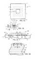
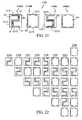
- FIG. 1Ashows PC board 1 having sides 2 , 3 , 4 , and 5 , top surface 6 , array 7 of structure for mounting discrete capacitors, and region 8 for mounting an IC.
- Each side of array 7defines plural rows, such as rows 9 and 10 .
- Each element of array 7represents mounting structure for mounting a discrete capacitor.
- Conventional PC boardsoften have an array including at least two rows of structure for mounting capacitors. Each row may have several to tens of array elements for mounting capacitors.
- the boardis designed so that capacitors mounted to the elements of array 7 sufficiently decouple the power to the IC from active circuitry so that the IC and any other coupled circuit elements functions as intended.
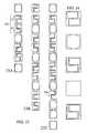
- FIG. 1Bshows a portion of board 1 , a source of electrical power 11 , a ground 12 , mounting structure 13 corresponding to one element of array 7 , mounting structure 14 corresponding to another element of array 7 , power plane 15 , and ground plane 16 .
- FIG. 1Bshows three vias extend down from each mounting structure element, such as vias 17 , 18 , 19 below mounting structure 13 . Use of more than two vias enables mounting unconventional devices, such as 3 terminal energy conditioners.
- power source 11distributes electrical power to circuit elements mounted to board 1 via conductive connection of power source 11 to power plane 15 .
- Ground plane 16conductively connects to ground 12 .
- Vias 17 and 19conductively connect to power plane 15 .
- Via 18does not conductively connect to power plane 15 and instead passes through an aperture in power plane 15 to ground plane 16 .
- Power plane 15is above ground plane 16 .
- FIG. 2Ashows assembly 200 including energy conditioner 201 mounted on board 1 .
- Board 1includes pads 202 , 203 , 204 that separate conditioner 201 from board surface 6 by a distance 205 as indicated by the distance between facing arrows 206 .
- Vias 17 , 18 , 19have a width 207 as indicated by the distance between facing arrows 209 .
- FIG. 2Bshows additional structure underneath conditioner 201 including additional power, ground, and/or signal planes 208 , 209 , 210 , and aperture 211 through which the conductive path in via 18 passes without shorting to power plane 15 .
- Additional power, ground and/or signal planesmay exist in any particular board.
- power feed from source 11 through one or more power planesprovides power for active circuitry in the IC mounted in region 8 to operate.
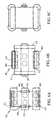
- FIG. 3Ashows conductive bands C
- FIG. 3Gshows conductive bands C, for purpose of discussion with energy conditioner internal structure disclosed herein below.
- FIG. 4A-4Oeach show one arrangement of conductive elements of mounting structure for mounting a single one of the novel discrete energy conditioners. These arrangements are also referred to as land patterns.
- the mounting surfacemay be a surface of a PC board, first level interconnect, or semiconductor chip.
- FIG. 4Ashows an arrangement 4 A of mounting surface structure including a set of three generally rectangularly shaped conductive pads 401 , 402 , 403 .
- Conductive pads 401 , 402 , 403have relatively long sides (unnumbered) and relatively short sides. The relatively short sides are labeled 401 A, 402 A, 403 A. Relatively short sides 401 A, 402 A, 403 A are aligned with one another such that a straight line segment could contact substantially all of short sides 401 A, 402 A, 403 A.
- Conductive pad 401contains vias 401 V 1 , 401 V 2 .
- Conductive pad 402contains vias 402 V 1 , 402 V 2 .
- Conductive pad 403contains vias 403 V 1 , 403 V 2 .
- Vias 401 V 1 , 402 V 1 , and 403 V 1are aligned such that a single line segment could intersect them.
- Vias 401 V 2 , 402 V 2 , and 403 V 2are aligned such that a single line segment could intersect them.
- padsmay have different sizes, lengths, or widths from one another.
- pad 402may be shorter than pads 401 , 403 .
- outer pads 401 , 403may have a different shape than central pad 402 .
- outer pads 401 , 403may include convex central regions and/or flared end regions.
- outer pads 401 , 403may be the same length as one another but shorter or longer than central pad 402 .
- certain viasmay have a diameter larger than the width or length of the pad to which they are attached such that the via is not entirely contained within the footprint of a conductive pad.
- a via diametermay be equal to a width of a conductive pad, 1.5, 2, or 3 times a width of the conductive pad.
- certain viasmay have different cross-sectional diameters from one.
- cross-section diameters of vias connecting to the central pad 402may be 1 ⁇ 3, 1 ⁇ 2, 1, 1.5, 2, or 3 times the cross-sectional diameter of vias connecting to outer pads 401 , 403 .
- vias 402 V 1 , 402 V 2may be spaced from one another by more than or less than the spacing between vias 401 V 1 , 401 V 2 and the spacing between 403 V 1 , 403 V 2 .
- each conductive padmay contain one, two, three, or more vias.
- each conductive pad 401 , 402 , 403may contain a single via.
- pads 401 and 403may contain 2 or 3 vias and pad 402 may contain one via.
- pads 401 and 403may contain 1 via and pad 402 may contain 2 or 3 vias.
- the padsmay not exist in which case just conductive vias exist in one of the foregoing arrangements. For example, two parallel rows of three vias.
- central pad 402may contain 1, 2, 3, or more vias and outer pads 401 , 403 may contain no vias.
- central pad 402may contain no vias and each outer pad 401 , 403 , may contain 1, 2, 3, or more vias.
- the cross-sections of viasmay not be circular, such as elliptical, elongated, or irregular.
- FIGS. 4B-4Lshow various arrangements of the alternatives discussed above.
- FIG. 4Bshows arrangement 4 B of mounting structure having vias of pad 402 more widely spaced from one another than the spacing between vias of either pad 401 or pad 403 .
- FIG. 4Cshows arrangement 4 C of mounting structure having vias having elongated elliptical cross-sections.
- FIG. 4Dshows arrangement 4 D of mounting structure having a single via in each one of pads 401 , 402 , 403 .
- FIG. 4Eshows arrangement 4 E of mounting structure having outer pads 401 , 403 having one centrally located via.
- FIG. 4Fshows arrangement 4 F of mounting structure having pads 401 , 402 , 403 having no vias.
- conductive linesmay radiate along the surface of the structure from each pad.
- FIG. 4Gshows arrangement 4 G of mounting structure having pads 401 , 402 , 403 each having three vias, each via in each pad aligned with one via in each one of the other two pads.
- FIG. 4Hshows arrangement 4 H of mounting structure having a single via in each pad, and in which the central pad 402 is short than the outer pads 401 , 403 .
- FIG. 4Ishows arrangement 4 I of mounting surface structure having equal length pads 401 , 402 , 403 , and in which the central pad 402 connects to only one via whereas the outer pads 401 , 402 connect to 2 vias.
- FIG. 4Jshows arrangement 4 J of mounting structure having three pairs of vias, and no pads.
- FIG. 4Kshows arrangement 4 K of mounting structure having outer pads 401 , 403 connecting to two vias and central pad 402 connecting to three vias.
- FIG. 4Lshows arrangement 4 L of mounting structure having central pad 402 connecting to one via and outer pads 401 , 403 having no vias.
- FIG. 4Mshows mounting structure 4 M having central pad 402 extending further than pads 401 , 403 , and vias in central pad 402 .
- FIG. 4Nshows mounting structure 4 N having via 501 having a larger diameter than via 502 . Moreover, larger via 501 is more centrally located than the other smaller diameter vias. That is, FIG. 5N contemplates benefits from conductively filled or lined vias of different dimensions from one another, and in which the larger vias are more centrally located relative to the energy conditioner to which they connect.
- FIG. 4Oshows mounting structure 4 O having central pad 402 extending symmetrically further than pads 401 , 403 .
- vias in each padare spaced symmetrically on either side of the center of the pad.
- the arrangement of viasis symmetric about the center point of central pad 402 .
- the inventorscontemplate all variations of arrangements of mounting structures (pads and vias combinations, sizes, and shapes) and energy conditioners mounted therein that provide conductive connection between the conductive elements of the mounting structure and A, B, and G master electrodes (defined herein below) internal to the energy conditioner.
- the A, B, and G master electrodeseither have regions forming part of the surface of the energy conditioner or internally physically contact conductive bands (outer electrodes) forming part of the surface of the energy conditioner.
- conductive band structures and mounting structurethat provide suitable connection to the A, B, and G master electrodes are contemplated.
- the inventorscontemplate all variations of energy conditioners lacking conductive band (outer electrodes) that can be mounted on and soldered (or conductively pasted) to the board thereby conductively connecting the A, B, and G master electrodes to the conductive regions of the mounting structure.
- conductive integration regionmeans either a conductive band or equivalent solder providing the contact to tabs of layers of a master electrode thereby conductively integrating those conductive layers to one master electrode.
- Tabsmean those portions of conductive layers of an internal structure of an energy conditioner that extend to the upper, lower, left or right side surfaces of the internal structure.
- Main body portions of conductive layers of an internal structuremeans those portions of the conductive layers that do not extend to the upper, lower, left or right side surfaces of the internal structure.
- the inventorscontemplate all combinations of the mounting structure configurations for mounting a conditioner to a surface and (1) either conductive band configurations or exposed A, B, and G master electrodes surfaces of energy conditioners that provide suitable connections for the A, B, and G master electrodes.
- novel energy conditioner and surface mounting structureprovide (1) a first conductive and mechanical contact, such as a solder connection, to at least one and more preferably all conductive bands connected to one side of the A and B master electrodes, (2) a second conductive and mechanical contact, such as a solder contact, to at least one and preferably all conductive bands connected to the opposite side of the A and B master electrodes, and (3) a third conductive contact to at least one and preferably all bands connected to both of the opposite ends of the G master electrode.
- the foregoing reference to electrical contactincludes situations where DC current is blocked, such as where a dielectric cap or layer exists somewhere along a via.
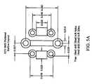
- FIG. 5Ashows geometric values and dimensions for one currently preferred mounting structure.
- FIG. 5Bshows geometric values and dimensions for another currently preferred mounting structure.
- 0603 X2Y type capacitorshave a capacitance of 1 to 100 nano farads, and nominal length, width, and thickness and height of 0.8, 0.6, 0.6, and 0.4 millimeters, respectively, as indicated for example by the URL:
- FIGS. 6A-6Beach schematically show a combination of a novel energy conditioner having a certain exterior surface structure in operable location on mounting structure.
- FIG. 6Ashows an arrangement 6 A of energy conditioner 601 on mounting structure 4 A.
- Conditioner 601had exterior surface structure 3 A.
- Conductive band C1is on top of conductive pad 401 .
- Part of conductive band C2is on top (since its ends extend beyond) of a first end of conductive pad 402 .
- Conductive band C3is on top of pad 403 .
- Conductive band C4is on top of a second end of conductive pad 402 .
- the first and second ends of conductive pad 402are on opposite sides of energy conditioner 601 from one another. Vias and portions of pads hidden from view are shown in dashed lines.
- FIG. 6Bshows arrangement 6 B of energy conditioner 602 mounted on arrangement 4 O of FIG. 4O .
- Conditioner 602also has exterior surface structure 3 A.
- Conductive band C1, C3contact near opposite ends of conductive pad 402 .
- Conductive bands C4, C2contact respectively to conductive pads 401 , 403 .
- FIG. 6Cshows arrangement 6 C of energy conditioner 603 mounted on mounting structure 4 J showing alignment of conductive bands of conditioner 603 , and also solder, on vias of mounting structure 4 J.
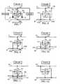
- FIGS. 7-12show circuits including an energy conditioner having A, B, and G master electrodes, which relate to the special properties of such conditioners.
- the inventorshave determined that connection of the G master electrode at at least two points, preferably at two points on opposite sides from one another, provides significant advantages. This is in spite of the fact that the G master electrode is a single conductive structure wherein location of connection would not be relevant in a lumped circuit representation.
- Circuit diagramsrely upon a lumped circuit model for accuracy of representation. In order to represent this geometric requirement relating to distributed circuit design in lumped circuit figures, the inventors schematically represent the energy conditioners as devices having at least 3 terminal device, with A, B, G terminals.
- More terminalsmay exist for each master electrode, and additional master electrodes may be integrated into the same component.
- the inventorshave also determined that relative locations of A, B, and G electrode terminals relative to the A, B, and G master electrode structures, may affect performance of the energy conditioners.
- FIG. 7-12therefore show circuits peculiar to this type of energy conditioner.
- external terminal Aconductively connects to the A master electrode
- external terminal Bconductively connects to the B master electrode
- external terminal G1conductively connects to the G master electrode. More specifically as used in FIGS. 7-12 , embodiments having at least 2 G external terminals, such as a G1 and G2, a first side of the G master electrode, and external terminal G2 conductively connects to a different side of the G master electrode.
- FIGS. 7-12each show conditioner 700 , and external terminals A, B, G1, and G2.
- the G master electrodesis represented by portions 702 , 705
- the A and B master electrodesare represented respective by flat plate elements 703 , 704 .
- the G master electrodeis spaced between or acts to shield the effects of charge buildup on the A master electrode from the B master electrode. This is schematically represented by the portion 702 of the G master electrode extending between the flat plate elements 703 , 704 of the A and B master electrodes.
- G master electrode portion 705schematically represents shielding by the G master electrode of the A and B master electrodes relative to space outside conditioner 700 .
- FIG. 7show a circuit 1 configuration for a conditioner 700 having A, B, and G master electrodes.
- external terminal Aconductively connects to node AS of conductive path S between a source of electrical power, SOURCE, and a load, LOAD.
- external terminal Bconductively connects to node BR of a return conductive path R between LOAD and SOURCE.
- external G1 and G2 terminalsboth conductively connect to a source of ground/constant potential P. Arrows above and below conductive paths between SOURCE and LOAD indicate that current flows in a loop.
- FIG. 8shows a circuit 2 configuration wherein external terminal A is tied to node AS on path S, external terminal B is tied to node BS also on path S, external terminal G1 is tied to node G1R on path R, and external terminal G2 is tied to node G2R also on path R.
- FIG. 9shows a circuit 3 configuration wherein external terminal A is tied to node AS on path S, external terminal B is tied to node BR on path R, external terminal G1 is tied to node G1R on path R, and external terminal G2 is tied to node G2R on path R.
- FIG. 10shows a circuit 4 configuration wherein external terminal A is tied to a node on path S, and external terminals G1, B, and G2 are tied to nodes on path R.
- FIG. 11shows a circuit 5 configuration wherein external terminal A is tied to a node on source path S1 from a source to a first load, L1, external terminal B is tied to a node S2 on a path from a source to a second load L2, and external terminals G1 and G2 are tied to a common return path CR.
- FIG. 12shows a circuit 6 configuration wherein external terminal A is tied to a node on path R (see element R in FIG. 7 ), external terminal B is tied to a node on path R, and external terminals G1 and G2 are tied to nodes on path S (see element S in FIG. 7 ).
- FIGS. 13-33generally show structure internal to the external surface 3 A to 3 K of FIGS. 3A-3K .
- the configuration of conductive layers of FIGS. 13-33can be arranged relative to the external surfaces 3 A to 3 K so that the conductive layers of the A master electrode contact the same conductive band or bands as one, the conductive layers of the B master electrode contact the same conductive band or bands as one, and the conductive layers of the G master electrode contact the same conductive band or bands as one.
- solder applied to the sides of the conditionersmay conductively contact the conductive layers of the A master electrode to one another, the conductive layers of the B master electrode to one another, and the conductive layers of the G master electrode to one another.
- the same solder contactsmay also contact corresponding conductive regions of the mounting structures shown in FIGS. 4A to 4O .
- plateherein generally is used to simplify explanation by defining a combination of a dielectric under layer with none, one, or more than one distinct conductive over layers.
- the relevant structureis the sequence of conductive layers separated by dielectric material.
- the hidden surface of the structures referred as plates in the following figuresrepresents a dielectric surface; that is, dielectric material vertically separating the defined conductive layers from one another.
- the structureare often formed by layering dielectric precursor material (green material) with conductive layer precursor material (conductive paste or the like), firing that layered structure at temperatures sufficient to convert the dielectric precursor to a desired structurally rigid dielectric material and to convert the conductive precursor layer to a high relatively conductivity (low resistivity) conductive layer.
- interconnects and semiconductor structureswould use different techniques, including conventional lithographic techniques, to fabricate equivalent or corresponding structures to those shown in FIGS. 13-25 , 27 , 29 , 31 , and 33 .
- the conductive bands and solder connections for stacked layers discussed herein belowwould in many cases be replaced by an array of conductively filled or lined vias selectively connecting conductive layers of the same master electrode to one another.
- those viaswould be spaced to selectively contact the tab regions of the A, B, and G layers discussed herein.
- a master electroderefers to the conductive layers or regions internal to an energy conditioner and the structure internal to the energy conditioner physically contacting those conductive layers or regions so that they form one integral conductive structure.
- Internal structure of energy conditionersincludes conductive layers or regions spaces by dielectric material from other conductive layers or regions.
- the conductive layers or regionseach have tab regions that extend to an edge or periphery of the dielectric material.
- An edge of each tab region of each conductive layeris contacted to external surface conductive structure.
- the external surface conductive structuremay be either conductive bands integral to the discrete energy conditioner or by solder employed also to mount the energy conditioner internal structure to mounting structure.
- tabs of those conductive layers or regionsare vertically aligned in the stack of layers so that a single conductive tab may conductively connect those conductive layers or regions to thereby form a master electrode.
- conductively filled or lined viasmay selectively connect to the same conductive layers or regions.
- Each one of the internal structures of energy conditioners shown in FIGS. 13-25 , 27 , 29 , 31 , and 33may reside in each one of external surface 3 A to 3 K of FIGS. 3A-3K in two distinct configurations.
- a first set of tabs of a G conductive layer of the G master electrodeare on the left and right sides (as shown in FIGS. 3A to 3K ) of the external surfaces 3 A to 3 K.
- the same first set of tabs of that same G conductive layer of the G master electrodeare on the upper and lower sides (as shown in FIGS. 3A to 3K ) of the external surfaces 3 A to 3 K.
- FIGS. 3A to 3KIn each configuration of the internal structures of energy conditioners shown in FIGS.
- the conductive layers of the A and B master electrodeseach have a region that extends into contact with at least one conductive band (or solder, when solder is applied) of the corresponding one of external surfaces 3 A to 3 K.
- the conductive layer or layers of the A master electrodedo not contact the same conductive band on external surfaces 3 A to 3 K as the conductive layer or layers of the B master electrode.
- the conductive layer or layers of the A master electrodedo not contact the same conductive band on external surfaces 3 A to 3 K as the conductive layer or layers of the G master electrode.
- the conductive layer or layers of the B master electrodedo not contact the same conductive band on external surfaces 3 A to 3 K as the conductive layer or layers of the G master electrode.
- FIGS. 13-33all show structures wherein a G master electrode has at least two distinct tabs.
- tabdoes not require a narrowing or necking compared to a body. Instead, it requires only extension to an edge of a dielectric structure.
- many of the conductive layers of G master electrodes shown in FIGS. 13-33include tab regions that are narrowed or necked compared to the region of the same conductive layer not adjacent the edge of dielectric structure.
- FIGS. 13-16 , 21 , 22 , 23show conductive layers of an A master electrode and conductive layers of a B master electrode that each have only have one distinct tab.
- FIGS. 17 , 18 , 19 , 24 , 25 , 27 , 29 , 31 , and 33show conductive layers of an A master electrode and conductive layers of a B master electrode that each have two distinct tabs.
- FIG. 20shows conductive layers of an A master electrode and conductive layers of a B master electrode that each have three distinct tabs.
- FIGS. 13 , 16 , 17 , 18 , 19 , 20 , 21 , 22 , 23 , and 24show plates having conductive layers of A and B master electrodes that extend to portions of at least three edges of their plate.
- FIGS. 13-25 , 27 , 29 , 31 , and 33show internal structure of novel energy conditioners.
- FIGS. 28 , 30 , and 32show external structure of novel energy conditioner embodiments of FIGS. 27 , 29 , and 31 , respectively;
- FIGS. 13-25 , 27 , 29 , and 31show plates that each have a conductive layer of an A master electrode and a conductive layer of a B master electrode in the same plate.
- FIGS. 13-24show stacks of plates that each have a conductive layer of an A master electrode and a conductive layer of a B master electrode in the same plate, and wherein two such plates are mirror images of one another about a line of symmetry extending vertically or horizontally in the plane of the paper of each figure.
- FIGS. 13-24show both (1) structures that each have a conductive layer of an A master electrode and a conductive layer of a B master electrode in the same plate and (2) stacks of plates wherein a conductive layer of an A master electrode on one plate has a region of substantial overlap with a conductive layer of a B master electrode on another plate.
- FIGS. 13-24show structures that include stacks of plates wherein (1) a first plate has a surface including a conductive layer of an A master electrode and a conductive layer of a B master electrode, (2) a second plate also has a surface including a conductive layer of an A master electrode and a conductive layer of a B master electrode, the conductive layer of the A master electrode in the first plate and the conductive layer of the B master electrode in the second plate have a region of substantial overlap, and (3) a third plate resides between the first two plates and has a conductive layer of a G master electrode extending throughout the region of substantial overlap.
- FIGS. 25 , 27 , and stacks 22 A and 22 B of FIG. 22show structures including only a single plate having a surface including a conductive layer of an A master electrode and a conductive layer of a B master electrode, and a single plate having a surface including a conductive layer of a G master electrode.
- FIGS. 29 and 31show structures including only a two plate each having a surface including a conductive layer of an A master electrode and a conductive layer of a B master electrode, and a single plate there between having a surface including a conductive layer of a G master electrode.
- FIGS. 21 , 22 , and 23show structures including at least one plate having a surface including a conductive layer of an A master electrode, a conductive layer of a B master electrode and a conductive layer of a G master electrode between the aforementioned conductive layers of the A and B master electrodes.
- FIG. 22 stacks 22 E and 22 G, and FIG. 23 stacks 23 A, 23 B, and 23 Ceach show structures including plates having a substantial region of a conductive layer of an A master electrode opposing a corresponding region of a conductive layer of a B master electrode on another plate having no intervening conductive layer of a G master electrode there between.
- FIG. 22 stack 22 H and FIG. 23 stack 23 Cshow structures in which the outermost conductive layers on one or both ends of the stack have a sequence of two or three conductive layers.
- FIG. 33shows a structure including a stack of plates wherein: (1) each plate has a surface including a conductive layer of only one master electrode, the sequence of conductive layers follows the pattern A, G, B, G, A, G, B; (2) conductive layers of the A and B master electrodes substantially overlap; (3) conductive layers of the G master electrode extend substantially throughout the area of overlap; (4) each conductive layer of the A master electrode has A tabs extends to front and back edges of the corresponding plate; (5) each conductive layer of the B master electrode has B tabs extends to front and back edges of the corresponding plate without overlapping any of the A tabs; and (6) each conductive layer of the G master electrode extends to left and right side edges of the corresponding plate.
- plates of a stack shown displaced horizontally or vertically in the pageexist in the stack in the sequence as expanded horizontally or vertically in the page.
- Each stackincludes a top and a bottom spaced from one another in a direction perpendicular to the face of the paper of the figures.
- each plate of each stackis shown in the figures as having in the plane of the paper a left side LS, right side RS, upper side US, and lower side LLS.
- FIG. 13shows stack 1300 of plates 1300 A, 1300 B, and 1300 C.
- Plate 1300 Aincludes dielectric material uniformly extending to the LS, RS, US, and LLS of stack 1300 .
- Conductive layer A1 designed to be part of the A master electrode and conductive layer B1 designed to be part of the B master electrodereside on the surface of dielectric material of plate 1300 A.
- Conductive layers A1 and B1are separated from one another by exposed dielectric surface D.
- Conductive layer A1has a tab A1T extending to the entire LS, and also the far left sides of the US and LLS.
- Conductive layer B1has a tab B1T extending to the entire RS, and also to the far right sides of the US and LLS.
- Conductive layer A1has a main body portion A1M extending the majority of the distance from the LS to the RS on the upper half of plate 1300 A.
- Conductive layer B1has a main body portion B1M extending the majority of the distance from the RS to the LS on the lower half of plate 1300 A.
- Plate 1300 Bincludes dielectric material on which resides conductive layer G1.
- Conductive layer G1has tab G1T1 extending to a central region of the US.
- Conductive layer G1has tab G1T2 extending to a central region of the LS.
- Conductive layer G1has a main body portion B1M between tabs G1T1 and G1T2.
- Plate 1300 Cincludes conductive layer A2 for the A master electrode, conductive layer B2 for the B master electrode. Conductive layers A2 and B2 are separated from one another by exposed dielectric surface D. Conductive layer A2 has a tab A2T extending to the entire LS, and also the far left sides of the US and LLS. Conductive layer B2 has a tab B2T extending to the entire RS, and also to the far right sides of the US and LLS. Conductive layer A2 has a main body portion A2M extending the majority of the distance from the LS to the RS on the lower half of plate 1300 A. Conductive layer B2 has a main body portion B2M extending the majority of the distance from the RS to the LS on the upper half of plate 1300 A.
- FIG. 14schematically shows the stack of layers 1300 C, 1300 B, 1300 A wherein main bodies A1M and B2M have a region of substantial overlap, and main bodies A2 and B1M have a region of substantial overlap, and conductive layer G1M extends over a substantial portion of the regions of overlap.
- the regions of overlapoccupy at least 20, more preferably at least 40 and more preferably at least 60 percent of the area of the A1M conductive layer.
- the G1M layerextends over at least 40, and more preferably at least 60 percent of the areas of overlap.
- FIGS. 13 and 14may be mounted to mounting structure on a PC board or interconnect, and soldered in place to complete the connections of the A, B, and G master electrodes.
- the structure of FIGS. 13 and 14may be fabricated with conductive bands forming a portion of the external structure thereby completing formation of the A, B, and G master electrodes.
- FIGS. 13 and 14are only exemplary of a sequence of layers forming an energy conditioner using the plates 1300 A, 1300 B, 1300 C.
- a stackmay have an integral number of repeats of the sequence 1300 A, 1300 B, 1300 C.
- a stackmay have the sequence 1300 A, 1300 B, 1300 C followed by any integral number of repeats of either the sequence 1300 B, 1300 C or the sequence 1300 A, 1300 B.
- one, two, or more than two 1300 B platesmay reside at either or both of the top and the bottom of a stack.
- FIGS. 15-20show alternative shapes for conductive layers of A, B, and G master electrodes wherein each plate having an conductive layer for an A master electrode also has a conductive layer for a B master electrode.
- the same alternatives and methods of assembly just noted for the FIGS. 13 and 14 embodimentapply to the FIGS. 15-20 stack embodiments.
- FIG. 15shows conductive layer A1M having tab A1T extending over only a portion of LS and over no other side.
- FIG. 16is identical to FIG. 13 .
- FIG. 17shows a stack of plates including plates 1700 A, 1700 B, and 1700 C.
- Plate 1700 Ahaving conductive layer A1M having tabs A1T1 and A1T2 separated by exposed dielectric D at the center of the LS.
- Plate 1700 Bincludes conductive layer of a G master electrode include main body portion G1M, and tab portions G1T1, G1T2, G1T3, and G1T4 in each side edge.
- Plate 1700 Cincludes conductive layers A2 and B2 for the A and B master electrodes respectively. Tabs of the A1 and A2 plated, the B1 and B2 plates in the stack are vertically aligned. Dielectric surface is exposed at the center of each side of plate 1700 A and 1700 C.
- the existence of exposed dielectric surfaces vertically aligned in the stack of plates, and existing on each side of the plates having conductive layers for the A and B electrodes,enables the existence of G tabs aligned on each side of the stack to be contacted by a conductive connecting material (conductive band or solder) without shorting the G tabs to the A or B tabs.
- the G1 layerhas only two tabs that extend to either the US and LLS or the LS and RS.
- FIG. 18shows a stack of plates wherein the conductive layers for the A master electrode each have two tabs, and those tabs are not completely aligned with one another.
- FIG. 18shows layer A1 and A2 having tabs A1T1 and A2T1 that only partially align at the left side of the US. Similarly the remaining tabs for the A and B layers have partial overlap.
- FIG. 19shows a stack similar to that shown in FIG. 18 except that extent of the tabs of the A1, B1, A2, and B2 layers is reduced so that the exposed dielectric D extends over the center of the LS and RS, and the G1 layer has four tabs two of which extend to the center of the LS and RS.
- the G1 layerhas only two tabs that extend to either the US and LLS or the LS and RS.
- FIG. 20shows a stack wherein the A1 layer has tabs that extend to portions of the LS, US, and LLS, but not to any corner, and not to the center of the LS.
- This configurationenables up to three separate conductive connections on the side of the stack to the A layer, and likewise to the B layer, for example with the external structure 3 K's left side and right side conductive bands connecting to the A and B layers.
- FIG. 21shows a stack 2100 including plates 2100 A, 2100 B, 2100 C, and 2100 D.
- Each one of plates 2100 A and 2100 Ccontain conductive layers for the A, B, and G master electrodes separated by dielectric D.
- Plate 2100 Aincludes conductive layer A1 that includes tab A1T1 extending over the entire LS and portions of the left end of the US and LLS.
- Plate 2100 Aalso includes conductive layer B1 that includes tab B1 extending over the entire RS and portions of the right end of the US and LLS.
- conductive layer G1that winds between the main body portions of A1 and B1 to tabs G1T1 and G1T2 in the center of the US and LLS.
- Plate 2100 Bincludes layer G2 having tabs G2T1 and G2T2 in the center of the US and LLS.
- Plate 2100 Cincludes layers A2, B2, and G3, and it is a mirror image of plate 2100 A.
- Plate 2100 Dis identical to plate 2100 B.
- the stack 2100has all tabs for the G layers aligned in the center of the US and LLS so that the G layers between A and B layers as well as the G layers above or below A and B layers are integrated into the G master electrode.
- stack sequencesare feasible, including the plate sequence 2100 A, 2100 B, 2100 C, and 2100 D followed or preceded by any number of repetitions of either 2100 C, 2100 D or 2100 A, 2100 B; by including 2 or more of plates of the form of 2100 B/ 2100 D instead of single plates, and not including the central G conductive layer in one, or alternating ones of the plates of the form 2100 A/ 2100 C, and including one, two, or more plates of the form of 2100 B/ 2100 D at one or both ends of the stack.
- FIG. 22shows stacks, 22 A to 22 H each including additional alternative stacks of the plates 2100 A to 2100 D. Note in particular that stacks 22 A, 22 B, and 22 C have less than 4 plates; one, two, and three plates or layers, respectively.
- FIG. 23shows stacks 23 A, 23 B, and 23 C which employ the same plates 2100 A, 2100 B, 2100 C, 2100 D as the stack of FIG. 21 .
- FIG. 23 's sequencediffers from the sequences in FIGS. 21 and 22 in that there are adjacent pair 2301 of mirror image layers M, M′ where overlap regions of conductive surfaces for A1 and B1 layers oppose one another without an intervening conductive layer for the G master electrode, like layers G2 and G4 of FIG. 21 .
- G conductive layerslike layers G2 and G4 do bracket a layer in which A, B, and G conductive layers reside, like plate 2302 .
- FIG. 23shows paired layers M, M′.
- stack sequencesmay include any number of repeats of the pair of M, M′ adjacent to one another with or without any of the layers having a single G layer, like layers G2 and G4 of FIG. 21 .
- FIG. 24shows a stack containing plates having various shapes from the preceding embodiments (a top plate having the same conductive pattern as the left side plate in FIG. 18 , a second from top plate having the conductive pattern of G1 in FIG. 13 , a third plate having the conductive pattern of a plate from FIG. 19 , a fourth plate representing a dielectric spacer region, and a fifth plate like the third plate) showing the plates of different shapes and sizes and of non-uniform spacings may exist in stacks contemplated by the inventors. All such modifications and variations of layers are within the scope contemplated.
- FIGS. 25-28are views of energy conditioners including conductive layers on only two planes and various external structures.
- FIG. 25shows stack 25 A containing plate 2500 A and 2500 B.
- An upper surface of plate 2500 Ais formed from surfaces of conductive layer A1, conductive layer B1, and exposed dielectric material D.
- An upper surface of plate 2500 Bis formed from conductive layer G1 and exposed dielectric material D.
- A1has tabs A1T1 near the left hand end of the US and A1T2 at near lower left hand end of the LLS.
- G1has tabs G1T1 in the middle of the US and G1T2 in the middle of the LLS.
- A1does not extent to the RS, and B1 does not extend to the LS.
- A1has main body portion AIM.
- B1has main body portion BIM.
- A1Mextends to a location closer to the US and RS than the LLS and LS.
- B1Mextends to a location closer to the LS and LLS than the US and RS.
- FIG. 26schematically shows an energy conditioner defined by one arrangement of (1) stack 25 A and (2) external structure 3 A of FIG. 3A .
- tabs A1T1 and A2T2contact internal surfaces of conductive band C1
- tabs G1T1 and G1T2respectively contact internal surfaces of bands C2 and C4
- tabs B1T1 and B1T2contact internal surfaces of conductive band C3.
- the third conductive integration structure and the fourth conductive integration structureform a single conductive band around the outer surface of said energy conditioner.
- FIGS. 28 , 30 , and 32The same alternative applies to FIGS. 28 , 30 , and 32 .
- FIG. 27shows stack 27 A including plates 2500 A and 2700 B.
- Plate 2700 Bdiffers from plate 2500 B in that the tabs G1T1 and G1T2 of layer G1 are in the LS and RS as opposed to the US and LLS.
- FIG. 28schematically shows an energy conditioner defined by one arrangement of (1) stack 27 A and (2) external structure 3 A of FIG. 3A .
- Tabs A1T1 and B1T1contact the internal surface of conductive band C3
- tabs A1 T2 and B1T2contact the internal surface of conductive band C1
- tab G1T1contacts the internal surface of conductive band C2
- tab G1T2contacts the internal surface of conductive band C4.
- the A and B master electrodesare conductively tied together at the edges of the tabs by conductive bands C1, C3.
- FIGS. 29-32are views of energy conditioners including conductive layers on three planes and various external structures.
- FIG. 29shows stack 29 A including plates 2500 A and 2500 B.
- Stack 29 Aalso includes another plate 2500 C (not shown) having the same layered pattern as plate 2500 A and on an opposite side of plate 2500 A relative to plate 2500 B.
- Plate 2500 Chas elements A2T1, A2T2, B2T1, B2T2, A2M, and B2M aligned with corresponding elements of plate 2500 A.
- Plate 2500 Chas conductive layers A2 and B2 having tabs aligned with corresponding tabs of plate 2500 A, including tab A2T1, A2T2, B2T1, and B2T2.
- plate 2500 Chas A1M and B1M as shown in FIG. 25 .
- plate 2500 Cmay be replaced by a plate having a conductive pattern that is a mirror image of the conductive pattern on plate 2500 A, the mirror defined by a vertical line passing through the center of conductive plate 2500 A.
- conductive tabs A1T1 and A2T2are still vertically aligned and conductively connected by contacts to the inner surface of conductive band C1.
- A1Mhas a substantial overlap with B2M
- A2Mhas a substantial overlap with B1M.
- FIG. 30schematically shows an energy conditioner defined by one arrangement of (1) stack 29 A and (2) external structure 3 A of FIG. 3A .
- tabs for conductive layers of the same master electrodeare aligned in the stack and contact conductive band structure.
- tabs A1T1 and A2T1are aligned and contact the internal surface of conductive band C1.
- A1Mhas a substantial overlap with B2M
- A2Mhas a substantial overlap with B1M.
- additional alternatives stacksinclude a repeating sequences of the three plates of layers of stack 29 A, and irregular sequences of 2500 A, 2500 B, and 2500 C, and the alternative to 2500 C noted above.
- FIG. 31shows stack 31 A including plates 2500 A and 2500 B.
- Stack 31 Aalso includes a second plate 2500 C having the same layered pattern as plate 2500 A and on an opposite side of plate 2500 A relative to plate 2500 B.
- Plate 2500 Chas conductive layers A2 and B2 having tabs aligned with corresponding tabs of plate 2500 A, including tab A2T1, A2T2, B2T1, and B2T2.
- FIG. 32schematically shows an energy conditioner defined by one arrangement of (1) stack 31 A and (2) external structure 3 A of FIG. 3A .
- tabs for conductive layers of the same master electrodeare aligned in the stack and contact conductive band structure.
- tabs A1T1 and A2T1are aligned and contact the internal surface of conductive band C1.
- plate 2500 Cmay be replaced by a plate having a conductive pattern that is a mirror image of the conductive pattern on plate 2500 A, the mirror defined by a vertical line passing through the center of conductive plate 2500 A.
- conductive tabs A1T1 and A2T2are still vertically aligned and conductively connected by contacts to the inner surface of conductive band C1.
- additional alternatives stacksinclude a repeating sequences of the three plates of layers of stack 29 A, and irregular sequences of 2500 A, 2500 B, and 2500 C, and the alternative to 2500 C noted above.
- FIG. 33shows stack 33 A including a sequence of plates 3300 A, 3300 B, 3300 C, 3300 B, 3300 A, 3300 B, 3300 C.
- Plates 3300 Aeach have an upper surface that consists of a surface of conductive layer A1 and exposed dielectric surface D.
- Conductive layer A1consists of tabs A1T1, A1T2, and main body portion AMB.
- Conductive layer A1is part of an A master electrode.
- Tab A1T1extends to the US near the LS.
- Tab A1T2extends to the LLS near the LS.
- AMBextends from tabs A1T1 and A1T2 towards the LS.
- Plates 3300 Beach have an upper surface that consists of a surface of conductive layer G1 and exposed dielectric surface D.
- Conductive layer G1consists of tabs G1T1, G1T2, and main body portion GMB.
- Tab G1T1extends to the middle of the LS.
- Tab G1T2extends to the middle of the RS.
- Plates 3300 Ceach have an upper surface that consists of a surface of conductive layer B1 and exposed dielectric surface D.
- Conductive layer B1consists of tabs B1T1, B1T2, and main body portion BMB.
- Conductive layer B1is part of a B master electrode.
- Tab B1T1extends to the US near the LS.
- Tab A1T2extends to the LLS near the LS.
- AMBextends from both tabs A1T1 and A1T2 towards the center.
- Stack 33 Aalso shows a dielectric plate having no conductive layers thereon at the top of the stack.
- the dielectric coverrepresents the condition that the conductive layers not be shorted to external conductive material, as might happen if they were otherwise uncovered.
- stack 33 Aincludes one or more repetitions of the sequence of plates 3300 A, 3300 B, 3300 C, 3300 B, 3300 A, 3300 B, 3300 C, and one or more repetitions of the sequence of plates 3300 A, 3300 B, 3300 C added to the top or the bottom of the sequence of plates 3300 A, 3300 B, 3300 C, 3300 B, 3300 A, 3300 B, 3300 C.
- Stack 33 Amay be assembled in a variety of external structures to provide various connections.
- one assembly of stack 33 A and external structure 3 I of FIG. 3Iresults in tabs A1T2 of the A1 conductive layers in contact with the internal surface of band C4, tabs A1T1 in contact with the internal surface of band C2, tabs B1T2 in contact with the internal surface of band C6, tabs B1T1 in contact with the internal surface of band C5, tabs G1T1 in contact with the internal surface of the LS of band C1, and tabs G1T2 in contact with the internal surface of the RS of band C3.
- stack 33 Ais assembled with either external structure 3 A or 3 G wherein the tabs of the G conductive layer contact internal surfaces of bands C2 and C4.
- band C1contacts to tabs at opposite ends of contact A conductive layer thereby forming two parallel conductive paths from tab A1T1 to tab A1T2; one directly between the tabs and the other through the connecting structure of band C1.
- two parallel conductive pathsare formed from B tabs of the same B layer by band C3.
Landscapes
- Engineering & Computer Science (AREA)
- Power Engineering (AREA)
- Microelectronics & Electronic Packaging (AREA)
- Manufacturing & Machinery (AREA)
- Physics & Mathematics (AREA)
- Electromagnetism (AREA)
- Structure Of Printed Boards (AREA)
- Connection Of Batteries Or Terminals (AREA)
- Battery Mounting, Suspending (AREA)
- Ceramic Capacitors (AREA)
- Battery Electrode And Active Subsutance (AREA)
- Secondary Cells (AREA)
- Inverter Devices (AREA)
- Dc-Dc Converters (AREA)
- Combinations Of Printed Boards (AREA)
- Fixed Capacitors And Capacitor Manufacturing Machines (AREA)
Abstract
Description
This application is a continuation of application Ser. No. 13/175,918, filed Jul. 4, 2011, which is a continuation of application Ser. No. 12/861,811, filed Aug. 23, 2010, now issued as U.S. Pat. No. 7,974,062, which is a continuation of application Ser. No. 11/817,634, filed Aug. 31, 2007, now issued as U.S. Pat. No. 7,782,587, which is a U.S. National Stage application of International Application PCT/US06/06607, filed Feb. 27, 2006, which claims the benefit of provisional Application No. 60/656,910, filed Mar. 1, 2005, provisional Application No. 60/661,002, filed Mar. 14, 2005, provisional Application No. 60/668,992, filed Apr. 7, 2005, provisional Application No. 60/671,107, filed Apr. 14, 2005, provisional Application No. 60/671,532, filed Apr. 15, 2005, provisional Application No. 60/674,284, filed Apr. 25, 2005, and provisional Application No. 60/751,273, filed Dec. 19, 2005.
The following applications are each incorporated by reference herein: application Ser. No. 13/175,918, filed Jul. 4, 2011, application Ser. No. 12/861,811, filed Aug. 23, 2010, application Ser. No. 11/817,634, filed Aug. 31, 2007, International Application PCT/US06/06607, filed Feb. 27, 2006, provisional Application No. 60/656,910, filed Mar. 1, 2005, provisional Application No. 60/661,002, filed Mar. 14, 2005, provisional Application No. 60/668,992, filed Apr. 7, 2005, provisional Application No. 60/671,107, filed Apr. 14, 2005, provisional Application No. 60/671,532, filed Apr. 15, 2005, provisional Application No. 60/674,284, filed Apr. 25, 2005, and provisional Application No. 60/751,273, filed Dec. 19, 2005.
This invention relates to energy conditioning.
Electrical circuits using low frequency electrical power generate noise that is coupled through the power distribution system. That noise is generally detrimental. In the past, capacitors have been used to condition the electrical power propagating to and from devices. One type of device in which capacitors have been used to condition electrical power is an active circuitry. Capacitors have been used to in active circuitry to decouple noise from the power lines. Typically, in applications involving Large or Very Large Scale Integration (LSI or VLSI) Integrated Circuits (ICs), multiple rows of capacitors are arrayed on a PC board as close as feasible to the location of the IC in the PC board, given design constraints. This arrangement provides sufficient decoupling of the power and ground from the IC's active circuitry. The terms “bypass” and “decoupling” are used interchangeable herein.
This application discloses novel energy conditioner structures and novel combinations of the connections of the energy conditioners on other structures, such as PC board structures, and novel circuit arrangements of the energy conditioners with structures, such as PC boards, described herein, generally provide improved decoupling, per conditioner, and require less conditioners and related structure, such as vias, to provide sufficient decoupling. Similarly to PC boards, the structures to which the novel conditioners and the novel combination of the connections of the energy conditioners may be applied include first level interconnects and semiconductor chips, including for example ASIC, FPGA, CPU, memory, transceiver, computer on a chip, and the like.
More particularly, this application discloses and claims energy conditioner internal structures and external structures, connection structure, and circuits including energy conditioners having A, B, and G master electrodes.
In one aspect, the claims define an internal structure of an energy conditioner:
wherein said internal structure has a left side surface, a right side surface, an upper side surface, a lower side surface, a top side surface, and a bottom side surface;
wherein said internal structure comprises a dielectric material and a conductive material;
wherein surfaces of said dielectric material and surfaces of said conductive material define said left side surface, said right side surface, said upper side surface, said lower side surface, said top side surface, and said bottom side surface;
wherein said conductive material comprises a first A conductive layer and a first B conductive layer in a first plane;
wherein said first A conductive layer and said first B conductive layer are electrically isolated from one another in said structure;
wherein said first A conductive layer comprises at least one first A conductive layer first tab and a first A conductive layer main body portion;
wherein said first B conductive comprises at least one first B conductive layer first tab and a first B conductive layer main body portion;
wherein said first A conductive layer main body portion does not extend to any one of said left side, right side, upper side, and lower side;
wherein said first B conductive layer main body portion does not extend to any one of said left side, right side, upper side, and lower side;
wherein said at least one first A conductive layer first tab extends to said left side surface, said upper side surface, and said lower side surface; and
wherein said at least one first B conductive layer first tab extends to at least portions of said right side surface, said upper side surface, and said lower side surface.
In aspects dependent upon the foregoing, the claims define wherein said first A conductive layer main body portion extends to a region closer to said right side surface than said left side surface and closer to said upper side surface than said lower side surface, and wherein said first B conductive layer main body portion extends to a region closer to said left side surface than said right side surface and closer to said lower side surface than said upper side surface; wherein said at least one first A conductive layer first tab comprises a single tab extending across all of said left side, extending to a left side end of said upper side surface, and extending to a left side end of said lower side surface; wherein said at least one first A conductive layer first tab comprises at least two tabs; wherein said conductive material further comprises a first G conductive layer; wherein conductive material further comprises a first G conductive layer between said first A conductive layer and said first B conductive layer; wherein conductive material further comprises a first G conductive layer in a second plane parallel to said first plane, and said G conductive layer has a G conductive layer main body portion having a region opposing at least a portion of said first A conductive layer A main body portion and a portion of said first B conductive layer main body portion;
wherein said conductive material comprises a second A conductive layer in a second plane and a second B conductive layer in said second plane;
wherein said second A conductive layer and said second B conductive layer are electrically isolated from one another in said structure;
wherein said second A conductive layer comprises at least one second A conductive layer first tab and a second A conductive layer main body portion;
wherein said second B conductive layer comprises at least one second B conductive layer first tab and a second B conductive layer main body portion;
wherein said second A conductive layer main body portion does not extend to any one of said left side surface, said right side surface, said upper side surface, and said lower side surface;
wherein said second B conductive layer main body portion does not extend to any one of said left side surface, said right side surface, said upper side surface, and said lower side surface;
wherein said at least one second A conductive layer first tab extends to at least portions of said left side surface, said upper side surface, and said lower side surface;
wherein said at least one second B conductive layer first tab extends to at least portions of said right side surface, said upper side surface, and said lower side surface;
wherein said second A conductive layer main body portion extends to a region closer to said right side surface than said left side surface and closer to said lower side surface than said upper side surface, and wherein said second B conductive layer main body portion extends to a region closer to said left side surface than said right side surface and closer to said upper side surface than said lower side surface;
whereby said first A conductive layer main body portion and said second B conductive layer main body portion have a first region of substantial overlap and said second A conductive layer main body portion and said first B conductive layer main body portion have a second region of substantial overlap; wherein said conductive material further comprises a first G conductive layer, and wherein said first G conductive layer comprises a main body portion having a substantial overlap with both said first region and said second region; wherein said first G conductive layer is in a third plane between said first plane and said second plane; wherein said conductive material further comprises:
a first G conductive layer in said first plane between said first A conductive layer and said first B conductive layer and electrically isolated in said structure from said first A conductive layer and said first B conductive layer; and
a second G conductive layer in said second plane between said second A conductive layer and said second B conductive layer and electrically isolated in said structure from said second A conductive layer and said second B conductive layer; wherein said conductive material further comprises a second G conductive layer, and wherein said second G conductive layer comprises a main body portion having a substantial overlap with both said first region and said second region; and wherein said first G conductive layer is in a third plane between said first plane and said second plane.
In a second aspect the claims define an assembly comprising said internal structure and an external structure of an energy conditioner, wherein said external structure comprises: a first conductive integration region that extends along at least one of said left side surface, said upper side surface, and said lower side surface and contacts there at, at least one of said at least one first A conductive layer first tab; and a second conductive integration region that extends along at least one of said right side surface, said upper side surface, and said lower side surface and contacts thereat at least one of said at least one first B conductive layer first tab.
Dependent upon the second aspect, the claims define wherein said internal structure further comprises a G conductive layer including a G conductive layer main body portion, a G conductive layer first tab, and a G conductive layer second tab, and wherein said external structure further comprises a third conductive integration region that extends along at least one side surface of said internal structure and contacts thereat said G conductive layer first tab; wherein said external structure further comprises a fourth conductive integration region that extends along at least one side surface of said internal structure opposite the one side surface of said internal structure along which said third conductive integration region extends where at said fourth conductive integration region contacts said G conductive layer second tab; wherein at least one of said first conductive integration region, said second conductive integration region, said third conductive integration region, and said fourth conductive integration region are formed from solder; wherein at least one of said first conductive integration region, said second conductive integration region, said third conductive integration region, and said fourth conductive integration region comprise a conductive band; further comprising a mounting structure to which said external structure is mounted, wherein said mounting structure consists of only a first conductive regions, a second conductive region, and a third conductive region; wherein said first conductive region comprises conductive material in a first via, said second conductive region comprises conductive material in a second via, and said third conductive region comprises conductive material in a third via.
In a third aspect the claims define a circuit comprising an internal structure of an energy conditioner having A and B layers in the same plane and tabs extending to at least three side surfaces; a source, and a load, wherein said internal structure is connected in said circuit in acircuit 1 configuration; a circuit comprising an internal structure of an energy conditioner having A and B layers in the same plane and tabs extending to at least three side surfaces, a source, and a load, wherein said internal structure is connected in said circuit in acircuit 2 configuration; a circuit comprising an internal structure of an energy conditioner having A, B, and G master electrode components, a source, and a load, wherein said internal structure is connected in said circuit in acircuit 3 configuration; a circuit comprising an internal structure of an energy conditioner having A, B, and G master electrode components, a first source, a second source, a first load, and a second load, wherein said internal structure is connected in said circuit in acircuit 4 configuration; a circuit comprising an internal structure of an energy conditioner having A, B, and G master electrode components, a first source, a first load, and a second load, wherein said internal structure is connected in said circuit in acircuit 5 configuration; a circuit comprising said internal structure of an energy conditioner having A, B, and G master electrode components, a first source, a first load, and a second load, wherein said internal structure is connected in said circuit in acircuit 6 configuration.
In additional aspects, the invention comprises an assembly having an energy conditioner having an internal structure, a mounting structure; and wherein said internal structure is mounted on said mounting structure; wherein said mounting structure comprises no more than three separate conductive elements; an assembly comprising: an energy conditioner having an internal structure including components of A, B, and G master electrodes, and an external structure comprising conductive regions that conductively connect components of the A master electrode to one another, components of the B master electrode to one another, and components of the G master electrode to one another; a mounting structure; wherein said internal structure is mounted on said mounting structure; wherein said mounting structure consists of only a first conductive region, a second conductive region, and a third conductive region; and wherein said A master electrode contacts said first conductive region, said B master electrode contacts said second conductive region, and said G master electrode contacts said third conductive region.
In additional aspects, the claims define that said G master electrode includes a first G conductive integration region that and a second G conductive integration region spatially separated and not contacting said first G conductive integration region, wherein both said a first G conductive integration region and said second G conductive integration region contact said third conductive region.
In another aspect, the claims define an internal structure of an energy conditioner: wherein said internal structure has a left side surface, a right side surface, an upper side surface, a lower side surface, a top side surface, and a bottom side surface; wherein said internal structure comprises a dielectric material and a conductive material; wherein surfaces of said dielectric material and surfaces of said conductive material define said left side surface, said right side surface, said upper side surface, said lower side surface, said top side surface, and said bottom side surface; wherein said conductive material comprises a stack of at least seven conductive layers in the following order from top to bottom: A1; G1; B1; G1; A1; G1; and B1; wherein each A1 conductive layer has an A1 first tab that extends to said upper side surface near said left side surface and an A2 tab that extends to said lower side surface near said left side surface; wherein each G1 conductive layer has a G1 first tab that extends to said left side surface and a G2 tab that extends to said right side surface near; and wherein each B1 conductive layer has a B1 first tab that extends to said upper side surface near said right side surface and a B2 tab that extends to said lower side surface near said right side surface. In dependent aspects, each tab of the same type has a vertical overlap with all other tabs of the same type, and conductive integration regions conductively connect layers of the same type only to one another; and wherein additional conductive layers exist within the seven layer sequence.
The figures show elements of embodiments of the inventions. The same reference number in different figures refers to identical elements or elements with similar structure or function.
Conventional capacitors are two terminal discrete devices.
In operation,power source 11 distributes electrical power to circuit elements mounted toboard 1 via conductive connection ofpower source 11 topower plane 15.Ground plane 16 conductively connects to ground12.Vias power plane 15. Via18 does not conductively connect topower plane 15 and instead passes through an aperture inpower plane 15 toground plane 16.Power plane 15 is aboveground plane 16.
In operation, power feed fromsource 11 through one or more power planes provides power for active circuitry in the IC mounted inregion 8 to operate. Conditioners mounted to the elements ofarray 7, one conditioner per array element, decouple transients otherwise induced in power due to switching and the like in the active circuitry of the IC.
In alternatives toarrangement 4A, pads may have different sizes, lengths, or widths from one another. For example, pad402 may be shorter thanpads
In another alternative toarrangement 4A,outer pads central pad 402. For example,outer pads outer pads central pad 402.
In another alternative toarrangement 4A, certain vias may have a diameter larger than the width or length of the pad to which they are attached such that the via is not entirely contained within the footprint of a conductive pad. For example, a via diameter may be equal to a width of a conductive pad, 1.5, 2, or 3 times a width of the conductive pad.
In another alternative toarrangement 4A, certain vias may have different cross-sectional diameters from one. For example, cross-section diameters of vias connecting to thecentral pad 402 may be ⅓, ½, 1, 1.5, 2, or 3 times the cross-sectional diameter of vias connecting toouter pads
In another alternative toarrangement 4A, vias402V1,402V2 may be spaced from one another by more than or less than the spacing between vias401V1,401V2 and the spacing between403V1,403V2.
In another alternative toarrangement 4A, each conductive pad may contain one, two, three, or more vias. For example, eachconductive pad pads pad 402 may contain one via. For example,pads pad 402 may contain 2 or 3 vias.
In another alternative toarrangement 4A, the pads may not exist in which case just conductive vias exist in one of the foregoing arrangements. For example, two parallel rows of three vias.
In another alternative toarrangement 4A, some pads may have connected vias and some may not. For example,central pad 402 may contain 1, 2, 3, or more vias andouter pads central pad 402 may contain no vias and eachouter pad
In another alternative toarrangement 4A, the cross-sections of vias may not be circular, such as elliptical, elongated, or irregular.
Preferably, vias in each pad are spaced symmetrically on either side of the center of the pad. Preferably, the arrangement of vias is symmetric about the center point ofcentral pad 402.
The inventors contemplate all variations of arrangements of mounting structures (pads and vias combinations, sizes, and shapes) and energy conditioners mounted therein that provide conductive connection between the conductive elements of the mounting structure and A, B, and G master electrodes (defined herein below) internal to the energy conditioner. The A, B, and G master electrodes either have regions forming part of the surface of the energy conditioner or internally physically contact conductive bands (outer electrodes) forming part of the surface of the energy conditioner. Thus, all variations of the conductive band structures and mounting structure that provide suitable connection to the A, B, and G master electrodes are contemplated. In addition, the inventors contemplate all variations of energy conditioners lacking conductive band (outer electrodes) that can be mounted on and soldered (or conductively pasted) to the board thereby conductively connecting the A, B, and G master electrodes to the conductive regions of the mounting structure.
Herein, conductive integration region, means either a conductive band or equivalent solder providing the contact to tabs of layers of a master electrode thereby conductively integrating those conductive layers to one master electrode. Tabs mean those portions of conductive layers of an internal structure of an energy conditioner that extend to the upper, lower, left or right side surfaces of the internal structure. Main body portions of conductive layers of an internal structure means those portions of the conductive layers that do not extend to the upper, lower, left or right side surfaces of the internal structure.
Thus, the inventors contemplate all combinations of the mounting structure configurations for mounting a conditioner to a surface and (1) either conductive band configurations or exposed A, B, and G master electrodes surfaces of energy conditioners that provide suitable connections for the A, B, and G master electrodes.
Some combinations of novel energy conditioner and surface mounting structure provide (1) a first conductive and mechanical contact, such as a solder connection, to at least one and more preferably all conductive bands connected to one side of the A and B master electrodes, (2) a second conductive and mechanical contact, such as a solder contact, to at least one and preferably all conductive bands connected to the opposite side of the A and B master electrodes, and (3) a third conductive contact to at least one and preferably all bands connected to both of the opposite ends of the G master electrode. The foregoing reference to electrical contact includes situations where DC current is blocked, such as where a dielectric cap or layer exists somewhere along a via.
It has been determined by numerical calculations that the values shown inFIGS. 5A and 5B provided superior decoupling when 0603 X2Y type energy conditioners are mounted thereto. 0603 X2Y type capacitors have a capacitance of 1 to 100 nano farads, and nominal length, width, and thickness and height of 0.8, 0.6, 0.6, and 0.4 millimeters, respectively, as indicated for example by the URL:
http://www.yageo.com/pdf/X2Y_series—10.pdf?5423212=EE8DCCAFD2263EBA74A64 43AF7A8BC75&4620207=.
InFIGS. 7-12 , external terminal A conductively connects to the A master electrode, external terminal B conductively connects to the B master electrode, external terminal G1 conductively connects to the G master electrode. More specifically as used inFIGS. 7-12 , embodiments having at least 2 G external terminals, such as a G1 and G2, a first side of the G master electrode, and external terminal G2 conductively connects to a different side of the G master electrode.
Relation of Internal Structure to External Structure of Energy Conditioners
Meaning of “Plate”, and Interconnector and IC Alternative Embodiments
The term “plate” herein generally is used to simplify explanation by defining a combination of a dielectric under layer with none, one, or more than one distinct conductive over layers. However, the relevant structure is the sequence of conductive layers separated by dielectric material. The hidden surface of the structures referred as plates in the following figures represents a dielectric surface; that is, dielectric material vertically separating the defined conductive layers from one another. In discrete energy conditioner component embodiments, the structure are often formed by layering dielectric precursor material (green material) with conductive layer precursor material (conductive paste or the like), firing that layered structure at temperatures sufficient to convert the dielectric precursor to a desired structurally rigid dielectric material and to convert the conductive precursor layer to a high relatively conductivity (low resistivity) conductive layer. However, embodiments formed in interconnects and semiconductor structures would use different techniques, including conventional lithographic techniques, to fabricate equivalent or corresponding structures to those shown inFIGS. 13-25 ,27,29,31, and33. Importantly, the conductive bands and solder connections for stacked layers discussed herein below would in many cases be replaced by an array of conductively filled or lined vias selectively connecting conductive layers of the same master electrode to one another. Preferably, those vias would be spaced to selectively contact the tab regions of the A, B, and G layers discussed herein.
Regardless of the mechanism of formation, it is the existence of the master electrodes' morphologies, assembly with external conductive structure, assembly with mounting structure, and integration into circuits 1-6 that are functionally important for decoupling.
Common Features of Internal Structure of Energy Conditioners
A master electrode refers to the conductive layers or regions internal to an energy conditioner and the structure internal to the energy conditioner physically contacting those conductive layers or regions so that they form one integral conductive structure.
Internal structure of energy conditioners includes conductive layers or regions spaces by dielectric material from other conductive layers or regions. The conductive layers or regions each have tab regions that extend to an edge or periphery of the dielectric material. An edge of each tab region of each conductive layer is contacted to external surface conductive structure. The external surface conductive structure may be either conductive bands integral to the discrete energy conditioner or by solder employed also to mount the energy conditioner internal structure to mounting structure. In energy conditioner internal structures having a plurality of conductive layers or regions designed to form a single master electrode, tabs of those conductive layers or regions are vertically aligned in the stack of layers so that a single conductive tab may conductively connect those conductive layers or regions to thereby form a master electrode.
Alternatively, or in addition to conductive bands or solder connecting to externally exposed edges of conductive layers or regions of a master electrode, conductively filled or lined vias may selectively connect to the same conductive layers or regions.
Relationship Between Internal Structures of Energy Conditioners and External Structure of Energy Conditioners
Each one of the internal structures of energy conditioners shown inFIGS. 13-25 ,27,29,31, and33 may reside in each one ofexternal surface 3A to3K ofFIGS. 3A-3K in two distinct configurations. In one configuration, a first set of tabs of a G conductive layer of the G master electrode are on the left and right sides (as shown inFIGS. 3A to 3K ) of theexternal surfaces 3A to3K. In the other configuration, the same first set of tabs of that same G conductive layer of the G master electrode are on the upper and lower sides (as shown inFIGS. 3A to 3K ) of theexternal surfaces 3A to3K. In each configuration of the internal structures of energy conditioners shown inFIGS. 13-25 ,27,29,31, and33 andexternal surfaces 3A to3K, the conductive layers of the A and B master electrodes each have a region that extends into contact with at least one conductive band (or solder, when solder is applied) of the corresponding one ofexternal surfaces 3A to3K.
Relationship Between Internal Structures of Energy Conditioners, External Structure of Energy Conditioners, and Circuits 1-6
At least in circuits wherein the A and B master electrode are not tied to the same conductive path of the circuit (circuits FIGS. 7-12 ), the conductive layer or layers of the A master electrode do not contact the same conductive band onexternal surfaces 3A to3K as the conductive layer or layers of the B master electrode.
At least in circuits wherein the A master electrode is not tied to the same conductive path of the circuit as the G master electrode (circuits 1-6; seeFIGS. 7-12 ), the conductive layer or layers of the A master electrode do not contact the same conductive band onexternal surfaces 3A to3K as the conductive layer or layers of the G master electrode.
At least in circuits wherein the B master electrode is not tied to the same conductive path of the circuit as the G master electrode (circuits FIGS. 7-12 ), the conductive layer or layers of the B master electrode do not contact the same conductive band onexternal surfaces 3A to3K as the conductive layer or layers of the G master electrode.
Features Common to Various Internal Structures Shown inFIGS. 13-33 .
In the following figures, plates of a stack shown displaced horizontally or vertically in the page exist in the stack in the sequence as expanded horizontally or vertically in the page. Each stack includes a top and a bottom spaced from one another in a direction perpendicular to the face of the paper of the figures. In addition, each plate of each stack is shown in the figures as having in the plane of the paper a left side LS, right side RS, upper side US, and lower side LLS.
The stack ofFIGS. 13 and 14 , once formed, may be mounted to mounting structure on a PC board or interconnect, and soldered in place to complete the connections of the A, B, and G master electrodes. Alternatively, the structure ofFIGS. 13 and 14 may be fabricated with conductive bands forming a portion of the external structure thereby completing formation of the A, B, and G master electrodes.
In one alternative external structure, the third conductive integration structure and the fourth conductive integration structure form a single conductive band around the outer surface of said energy conditioner. The same alternative applies toFIGS. 28 ,30, and32.
Alternatively, forFIG. 29 , and stack29A, plate2500C may be replaced by a plate having a conductive pattern that is a mirror image of the conductive pattern onplate 2500A, the mirror defined by a vertical line passing through the center ofconductive plate 2500A. In this alternative, conductive tabs A1T1 and A2T2, for example, are still vertically aligned and conductively connected by contacts to the inner surface of conductive band C1. However, in this alternative, A1M has a substantial overlap with B2M, and A2M has a substantial overlap with B1M.
Alternatively, forFIG. 31 , plate2500C may be replaced by a plate having a conductive pattern that is a mirror image of the conductive pattern onplate 2500A, the mirror defined by a vertical line passing through the center ofconductive plate 2500A. In this alternative, conductive tabs A1T1 and A2T2, for example, are still vertically aligned and conductively connected by contacts to the inner surface of conductive band C1. As with other embodiments, additional alternatives stacks include a repeating sequences of the three plates of layers ofstack 29A, and irregular sequences of2500A,2500B, and2500C, and the alternative to2500C noted above.
Alternatives to stack33A include one or more repetitions of the sequence ofplates plates plates
In alternatives assemblies,stack 33A is assembled with eitherexternal structure
The foregoing describe embodiments and alternatives within the scope of the novel concepts disclosed herein. The following claims define the scope of protection sought.
Claims (1)
1. A conductive structure, comprising:
[A] a plurality of aligned structural plates that are positioned and stacked in a vertical alignment with one another, and wherein each one of the aligned structural plates in the plurality has
1) substantially the same width and length, and
2) a left side, a right side, an upper side, and a lower side, and has a left side, a right side, an upper side, and a lower side;
[B] an upper structural plate of the plurality comprising an upper layer of dielectric and an upper layer of conductive material;
[C] a first structural plate of the plurality, comprising a first support layer of dielectric and a first layer of conductive material that includes
1) a first-shaped electrode layer area including a left region and an upper region, and wherein the left region extends along, but not beyond, the left side of the first structural plate, and
2) a second-shaped electrode layer including a right region and a lower region, and wherein the right region extends along, but not beyond, the right side of the first structural plate;
[D] an center structural plate of the plurality comprising an center layer of dielectric and a center layer of conductive material;
[E] a second structural plate of the plurality, comprising a second support layer of dielectric and an second layer of conductive material that includes
1) a first-shaped electrode layer area including a left region and an upper region, and wherein the left region extends along, but not beyond, the left side of the second structural plate, and
2) a second-shaped electrode layer including a right region and a lower region, and wherein the right region extends along, but not beyond, the right side of the second structural plate;
[F] an lower structural plate of the plurality comprising an lower layer of dielectric and a lower layer of conductive material;
wherein
(a) the first and second structural plates are parallel with one another,
(b) the first and second-shaped electrode layers of the first structural plate are co-planar and electrically isolated from each other,
(c) the first and second-shaped electrode layers of the second structural plate are co-planar and electrically isolated from each other,
(d) the upper structural plate and the center structural plate sandwich the first structural plate,
(e) the center structural plate and the lower structural plate sandwich the second structural plate,
(f) the upper structural plate and the lower structural plate sandwich the first structural plate, the central structural plate and the second structural plate therebetween, and
(g) within the plurality of aligned structural plates, the orientation of the first and second-shaped electrode layers of the first structural plate is 180 degrees opposite the orientation of the first and second-shaped electrode layers of the second structural plate.
Priority Applications (1)
| Application Number | Priority Date | Filing Date | Title |
|---|---|---|---|
| US14/042,637US9001486B2 (en) | 2005-03-01 | 2013-09-30 | Internally overlapped conditioners |
Applications Claiming Priority (12)
| Application Number | Priority Date | Filing Date | Title |
|---|---|---|---|
| US65691005P | 2005-03-01 | 2005-03-01 | |
| US66100205P | 2005-03-14 | 2005-03-14 | |
| US66899205P | 2005-04-07 | 2005-04-07 | |
| US67110705P | 2005-04-14 | 2005-04-14 | |
| US67153205P | 2005-04-15 | 2005-04-15 | |
| US67428405P | 2005-04-25 | 2005-04-25 | |
| US75127305P | 2005-12-19 | 2005-12-19 | |
| PCT/US2006/006607WO2006093830A2 (en) | 2005-03-01 | 2006-02-27 | Internally overlapped conditioners |
| US81763407A | 2007-08-31 | 2007-08-31 | |
| US12/861,811US7974062B2 (en) | 2005-03-01 | 2010-08-23 | Internally overlapped conditioners |
| US13/175,918US8547677B2 (en) | 2005-03-01 | 2011-07-04 | Method for making internally overlapped conditioners |
| US14/042,637US9001486B2 (en) | 2005-03-01 | 2013-09-30 | Internally overlapped conditioners |
Related Parent Applications (1)
| Application Number | Title | Priority Date | Filing Date |
|---|---|---|---|
| US13/175,918ContinuationUS8547677B2 (en) | 2005-03-01 | 2011-07-04 | Method for making internally overlapped conditioners |
Publications (2)
| Publication Number | Publication Date |
|---|---|
| US20140104747A1 US20140104747A1 (en) | 2014-04-17 |
| US9001486B2true US9001486B2 (en) | 2015-04-07 |
Family
ID=36941668
Family Applications (5)
| Application Number | Title | Priority Date | Filing Date |
|---|---|---|---|
| US11/817,639Expired - Fee RelatedUS7630188B2 (en) | 2005-03-01 | 2006-02-27 | Conditioner with coplanar conductors |
| US11/817,634Expired - Fee RelatedUS7782587B2 (en) | 2005-03-01 | 2006-02-27 | Internally overlapped conditioners |
| US12/861,811Expired - Fee RelatedUS7974062B2 (en) | 2005-03-01 | 2010-08-23 | Internally overlapped conditioners |
| US13/175,918Expired - Fee RelatedUS8547677B2 (en) | 2005-03-01 | 2011-07-04 | Method for making internally overlapped conditioners |
| US14/042,637Expired - Fee RelatedUS9001486B2 (en) | 2005-03-01 | 2013-09-30 | Internally overlapped conditioners |
Family Applications Before (4)
| Application Number | Title | Priority Date | Filing Date |
|---|---|---|---|
| US11/817,639Expired - Fee RelatedUS7630188B2 (en) | 2005-03-01 | 2006-02-27 | Conditioner with coplanar conductors |
| US11/817,634Expired - Fee RelatedUS7782587B2 (en) | 2005-03-01 | 2006-02-27 | Internally overlapped conditioners |
| US12/861,811Expired - Fee RelatedUS7974062B2 (en) | 2005-03-01 | 2010-08-23 | Internally overlapped conditioners |
| US13/175,918Expired - Fee RelatedUS8547677B2 (en) | 2005-03-01 | 2011-07-04 | Method for making internally overlapped conditioners |
Country Status (5)
| Country | Link |
|---|---|
| US (5) | US7630188B2 (en) |
| JP (2) | JP2008535207A (en) |
| KR (2) | KR20070107747A (en) |
| GB (2) | GB2439861A (en) |
| WO (2) | WO2006093830A2 (en) |
Cited By (5)
| Publication number | Priority date | Publication date | Assignee | Title |
|---|---|---|---|---|
| US10431388B2 (en) | 2015-12-08 | 2019-10-01 | Avx Corporation | Voltage tunable multilayer capacitor |
| US10607777B2 (en) | 2017-02-06 | 2020-03-31 | Avx Corporation | Integrated capacitor filter and integrated capacitor filter with varistor function |
| US10840027B2 (en) | 2017-09-08 | 2020-11-17 | Avx Corporation | High voltage tunable multilayer capacitor |
| US10943741B2 (en) | 2017-10-02 | 2021-03-09 | Avx Corporation | High capacitance tunable multilayer capacitor and array |
| US11295899B2 (en) | 2018-12-26 | 2022-04-05 | KYOCERA AVX Components Corporation | System and method for controlling a voltage tunable multilayer capacitor |
Families Citing this family (20)
| Publication number | Priority date | Publication date | Assignee | Title |
|---|---|---|---|---|
| US7321485B2 (en) | 1997-04-08 | 2008-01-22 | X2Y Attenuators, Llc | Arrangement for energy conditioning |
| US6603646B2 (en) | 1997-04-08 | 2003-08-05 | X2Y Attenuators, Llc | Multi-functional energy conditioner |
| US9054094B2 (en) | 1997-04-08 | 2015-06-09 | X2Y Attenuators, Llc | Energy conditioning circuit arrangement for integrated circuit |
| US7301748B2 (en) | 1997-04-08 | 2007-11-27 | Anthony Anthony A | Universal energy conditioning interposer with circuit architecture |
| US7336468B2 (en)* | 1997-04-08 | 2008-02-26 | X2Y Attenuators, Llc | Arrangement for energy conditioning |
| WO2006093831A2 (en) | 2005-03-01 | 2006-09-08 | X2Y Attenuators, Llc | Energy conditioner with tied through electrodes |
| JP2008535207A (en) | 2005-03-01 | 2008-08-28 | エックストゥーワイ アテニュエイターズ,エルエルシー | Regulator with coplanar conductor |
| WO2006099297A2 (en) | 2005-03-14 | 2006-09-21 | X2Y Attenuators, Llc | Conditioner with coplanar conductors |
| WO2007103965A1 (en)* | 2006-03-07 | 2007-09-13 | X2Y Attenuators, Llc | Energy conditioner structures |
| JP5605342B2 (en)* | 2010-11-09 | 2014-10-15 | 株式会社村田製作所 | Electronic components and board modules |
| TW201316895A (en)* | 2011-10-14 | 2013-04-16 | Hon Hai Prec Ind Co Ltd | Printed circuit board capable of preventing electromagnetic interface |
| US9146888B2 (en)* | 2012-07-05 | 2015-09-29 | Apple Inc. | Techniques for monitoring contacts in a connector |
| JP2015049986A (en)* | 2013-08-30 | 2015-03-16 | 富士通株式会社 | Connector and manufacturing method therefor |
| JP5958479B2 (en)* | 2014-01-31 | 2016-08-02 | 株式会社村田製作所 | Electronic component mounting structure |
| US20150223323A1 (en)* | 2014-02-05 | 2015-08-06 | Colin Patrick O'Flynn | Footprint for Prototyping High Frequency Printed Circuit Boards |
| JP2016127262A (en)* | 2014-12-26 | 2016-07-11 | 太陽誘電株式会社 | Through-type multilayer ceramic capacitors |
| JP2016149479A (en)* | 2015-02-13 | 2016-08-18 | 株式会社村田製作所 | Multilayer capacitor |
| JP2022530506A (en) | 2019-05-01 | 2022-06-29 | バード・アクセス・システムズ,インコーポレーテッド | Puncture devices, puncture systems including puncture devices, and their methods |
| JP2021103730A (en)* | 2019-12-25 | 2021-07-15 | 太陽誘電株式会社 | Ceramic electronic component and mounting board |
| WO2021187409A1 (en)* | 2020-03-19 | 2021-09-23 | ローム株式会社 | Semiconductor device |
Citations (860)
| Publication number | Priority date | Publication date | Assignee | Title |
|---|---|---|---|---|
| US676185A (en) | 1896-03-28 | 1901-06-11 | Franz Gattinger | Lightning-protector for electrical apparatus. |
| US3104363A (en) | 1960-07-25 | 1963-09-17 | Sanders Associates Inc | Strip transmission line crossover having reduced impedance discontinuity |
| US3240621A (en) | 1960-11-14 | 1966-03-15 | Dictaphone Corp | High viscosity dispersions of magnetic pigments |
| US3273027A (en) | 1962-09-19 | 1966-09-13 | Johnson Matthey & Mallory Ltd | Three-terminal electrolytic device |
| CA747079A (en) | 1966-11-22 | P. Halverson Richard | Magnetic thin film memory system | |
| US3343034A (en) | 1961-06-21 | 1967-09-19 | Energy Conversion Devices Inc | Transient suppressor |
| US3379943A (en) | 1966-01-17 | 1968-04-23 | American Lava Corp | Multilayered electrical capacitor |
| US3381244A (en) | 1966-02-09 | 1968-04-30 | Bell Telephone Labor Inc | Microwave directional coupler having ohmically joined output ports d.c. isolated from ohmically joined input and terminated ports |
| US3488528A (en) | 1966-05-06 | 1970-01-06 | Philips Corp | Integrated circuit |
| US3496434A (en) | 1968-11-22 | 1970-02-17 | Sprague Electric Co | High voltage ceramic capacitor |
| US3519959A (en) | 1966-03-24 | 1970-07-07 | Burroughs Corp | Integral electrical power distribution network and component mounting plane |
| US3534301A (en) | 1967-06-12 | 1970-10-13 | Bell Telephone Labor Inc | Temperature compensated integrated circuit type narrowband stripline filter |
| US3568000A (en) | 1967-11-22 | 1971-03-02 | Comp Generale Electricite | Multilayer printed circuit |
| US3573677A (en) | 1967-02-23 | 1971-04-06 | Litton Systems Inc | Connector with provision for minimizing electromagnetic interference |
| US3652941A (en) | 1970-02-24 | 1972-03-28 | Rhg Electronics Lab Inc | Double balanced microwave mixer using balanced microstrip baluns |
| US3680005A (en) | 1966-03-24 | 1972-07-25 | Burroughs Corp | Integral electrical power distribution network having stacked plural circuit planes of differing characteristic impedance with intermediate ground plane for separating circuit planes |
| US3681612A (en) | 1970-06-19 | 1972-08-01 | Siemens Ag | Device for eliminating interference between conductors of high frequency signals |
| US3688361A (en) | 1971-06-18 | 1972-09-05 | Gulton Ind Inc | Method of making a trimmable monolithic capacitor |
| US3691563A (en) | 1970-12-11 | 1972-09-12 | Motorola Inc | Dual band stripline antenna |
| US3701958A (en) | 1969-12-17 | 1972-10-31 | Saba Gmbh | Multisection bandpass filter from small signal circuits |
| US3736471A (en) | 1970-11-18 | 1973-05-29 | I Honeywell Bull Soc | Assemblage element for functional unit with card connector means |
| US3740678A (en) | 1971-03-19 | 1973-06-19 | Ibm | Strip transmission line structures |
| US3742420A (en) | 1971-10-21 | 1973-06-26 | J Harnden | Protective electrical feed through assemblies for enclosures for electrical devices |
| US3764727A (en) | 1972-06-12 | 1973-10-09 | Western Electric Co | Electrically conductive flat cable structures |
| US3790858A (en) | 1973-01-29 | 1974-02-05 | Itt | Electrical connector with component grounding plate |
| US3842374A (en) | 1973-03-09 | 1974-10-15 | Allen Bradley Co | Feedthrough filter with non-linear resistive dielectric |
| US3880493A (en) | 1973-12-28 | 1975-04-29 | Burroughs Corp | Capacitor socket for a dual-in-line package |
| US3896354A (en) | 1974-07-02 | 1975-07-22 | Sprague Electric Co | Monolithic ceramic capacitor |
| US3898541A (en) | 1973-12-17 | 1975-08-05 | Vitramon Inc | Capacitors and method of adjustment |
| US3921041A (en) | 1975-02-24 | 1975-11-18 | American Radionic | Dual capacitor |
| US4023071A (en) | 1975-06-09 | 1977-05-10 | Fussell Gerald W | Transient and surge protection apparatus |
| US4030190A (en) | 1976-03-30 | 1977-06-21 | International Business Machines Corporation | Method for forming a multilayer printed circuit board |
| US4071878A (en) | 1975-02-18 | 1978-01-31 | N L Industries, Inc. | Method for producing capacitors and ceramic body therefore |
| US4081770A (en) | 1973-10-29 | 1978-03-28 | Ferdy Mayer | Capacitive electric filter |
| US4119084A (en) | 1977-05-11 | 1978-10-10 | Eckels Robert E | Building with passive solar energy conditioning |
| US4135132A (en) | 1976-02-27 | 1979-01-16 | Telefonaktiebolaget L M Ericsson | Passive filter compensation network |
| US4139783A (en) | 1975-09-02 | 1979-02-13 | General Electric Company | Single phase signal processing system utilizing charge transfer devices |
| US4148003A (en) | 1977-07-08 | 1979-04-03 | Globe-Union Inc. | Series feed-through capacitor |
| US4160220A (en) | 1978-01-23 | 1979-07-03 | Rca Corporation | Precision microwave delay circuit and method |
| US4191986A (en) | 1978-05-12 | 1980-03-04 | The United States Of America As Represented By The Secretary Of The Navy | Power line transient suppressors |
| US4198613A (en) | 1978-05-17 | 1980-04-15 | Bunker Ramo Corporation | Filter contact |
| US4237522A (en) | 1979-06-29 | 1980-12-02 | International Business Machines Corporation | Chip package with high capacitance, stacked vlsi/power sheets extending through slots in substrate |
| US4259604A (en) | 1977-09-17 | 1981-03-31 | Canon Kabushiki Kaisha | DC rotary machine |
| US4262317A (en) | 1979-03-22 | 1981-04-14 | Reliable Electric Company | Line protector for a communications circuit |
| US4275945A (en) | 1979-08-31 | 1981-06-30 | The Bendix Corporation | Filter connector with compound filter elements |
| US4290041A (en) | 1978-02-10 | 1981-09-15 | Nippon Electric Co., Ltd. | Voltage dependent nonlinear resistor |
| US4292558A (en) | 1979-08-15 | 1981-09-29 | Westinghouse Electric Corp. | Support structure for dynamoelectric machine stators spiral pancake winding |
| US4308509A (en) | 1979-01-26 | 1981-12-29 | Sony Corporation | Filter circuit utilizing charge transfer device |
| US4312023A (en) | 1979-03-23 | 1982-01-19 | L.C.C.-C.I.C.E. Compagnie Europeenne De Composants Electroniques | Ceramic power capacitor |
| US4312026A (en) | 1979-04-11 | 1982-01-19 | Tdk Electronics Co., Ltd. | Chip ceramic capacitor |
| US4320364A (en) | 1979-06-11 | 1982-03-16 | Murata Manufacturing Co., Ltd. | Capacitor arrangement |
| US4322698A (en) | 1978-12-28 | 1982-03-30 | Tetsuo Takahashi | Laminated electronic parts and process for making the same |
| US4328530A (en) | 1980-06-30 | 1982-05-04 | International Business Machines Corporation | Multiple layer, ceramic carrier for high switching speed VLSI chips |
| US4328531A (en) | 1979-03-30 | 1982-05-04 | Hitachi, Ltd. | Thick film multilayer substrate |
| US4335417A (en) | 1978-09-05 | 1982-06-15 | General Electric Company | Heat sink thermal transfer system for zinc oxide varistors |
| US4342143A (en) | 1974-02-04 | 1982-08-03 | Jennings Thomas A | Method of making multiple electrical components in integrated microminiature form |
| US4349862A (en) | 1980-08-11 | 1982-09-14 | International Business Machines Corporation | Capacitive chip carrier and multilayer ceramic capacitors |
| US4353044A (en) | 1980-01-21 | 1982-10-05 | Siemens Aktiengesellschaft | Switched-capacitor filter circuit having at least one simulated inductor and having a resonance frequency which is one-sixth of the sampling frequency |
| US4353040A (en) | 1979-10-06 | 1982-10-05 | International Business Machines Corporation | Multi-layer module with constant characteristic impedance |
| JPS57172130U (en) | 1981-04-24 | 1982-10-29 | ||
| US4366456A (en) | 1979-06-14 | 1982-12-28 | Fujitsu Limited | Switched-capacitor filter |
| US4374368A (en) | 1980-12-29 | 1983-02-15 | Sperry Corporation | Multilevel stripline transition |
| US4375053A (en) | 1980-12-29 | 1983-02-22 | Sperry Corporation | Interlevel stripline coupler |
| FR2496970B1 (en) | 1980-12-18 | 1983-04-15 | Eurofarad | |
| US4384263A (en) | 1981-04-02 | 1983-05-17 | Corcom, Inc. | Leadless filter |
| US4394639A (en) | 1978-12-18 | 1983-07-19 | Mcgalliard James D | Printed circuit fuse assembly |
| US4412146A (en) | 1974-07-13 | 1983-10-25 | Fuetterer Bodo | Electric motor control |
| US4424552A (en) | 1981-06-05 | 1984-01-03 | L.C.C.-C.I.C.E. Compagnie Europeene De Composants Electroniques | Condenser block and voltage multiplier comprising such a condenser block |
| US4441088A (en) | 1981-12-31 | 1984-04-03 | International Business Machines Corporation | Stripline cable with reduced crosstalk |
| US4494083A (en) | 1981-06-30 | 1985-01-15 | Telefonaktiebolaget L M Ericsson | Impedance matching stripline transition for microwave signals |
| US4494092A (en) | 1982-07-12 | 1985-01-15 | The Deutsch Company Electronic Components Division | Filter pin electrical connector |
| US4498122A (en) | 1982-12-29 | 1985-02-05 | At&T Bell Laboratories | High-speed, high pin-out LSI chip package |
| US4533931A (en) | 1983-02-07 | 1985-08-06 | Murata Manufacturing Co., Ltd. | Reduction reoxidation type semiconductor ceramic condenser |
| US4541035A (en) | 1984-07-30 | 1985-09-10 | General Electric Company | Low loss, multilevel silicon circuit board |
| US4551746A (en) | 1982-10-05 | 1985-11-05 | Mayo Foundation | Leadless chip carrier apparatus providing an improved transmission line environment and improved heat dissipation |
| US4551747A (en) | 1982-10-05 | 1985-11-05 | Mayo Foundation | Leadless chip carrier apparatus providing for a transmission line environment and improved heat dissipation |
| US4553114A (en) | 1983-08-29 | 1985-11-12 | Amp Incorporated | Encapsulated printed circuit board filter |
| US4556929A (en) | 1983-07-08 | 1985-12-03 | Murata Manufacturing Co. Ltd. | Multi-layer ceramic capacitor |
| US4560962A (en) | 1983-08-30 | 1985-12-24 | Burroughs Corporation | Multilayered printed circuit board with controlled 100 ohm impedance |
| US4563659A (en) | 1982-07-28 | 1986-01-07 | Murata Manufacturing Co., Ltd. | Noise filter |
| US4577214A (en) | 1981-05-06 | 1986-03-18 | At&T Bell Laboratories | Low-inductance power/ground distribution in a package for a semiconductor chip |
| US4586104A (en) | 1983-12-12 | 1986-04-29 | Rit Research Corp. | Passive overvoltage protection devices, especially for protection of computer equipment connected to data lines |
| US4587589A (en) | 1983-03-21 | 1986-05-06 | Bbc Brown, Boveri & Company, Limited | Voltage limiting feed-through unit |
| US4590537A (en) | 1983-09-11 | 1986-05-20 | Murata Manufacturing Co., Ltd. | Laminated capacitor of feed-through type |
| US4592606A (en) | 1984-09-20 | 1986-06-03 | Zenith Electronics Corporation | Breakaway jumper edge connector |
| US4597029A (en) | 1984-03-19 | 1986-06-24 | Trilogy Computer Development Partners, Ltd. | Signal connection system for semiconductor chip |
| US4612140A (en) | 1983-04-08 | 1986-09-16 | Murata Manufacturing Co., Ltd. | Non-linear electrical resistor having varistor characteristics |
| US4612497A (en) | 1985-09-13 | 1986-09-16 | Motorola, Inc. | MOS current limiting output circuit |
| US4626958A (en) | 1985-01-22 | 1986-12-02 | Rogers Corporation | Decoupling capacitor for Pin Grid Array package |
| US4628411A (en) | 1984-03-12 | 1986-12-09 | International Business Machines Corporation | Apparatus for directly powering a multi-chip module from a power distribution bus |
| US4633368A (en) | 1985-10-31 | 1986-12-30 | Integrated Power Components | Multiple function integrated capacitor |
| US4636752A (en) | 1984-06-08 | 1987-01-13 | Murata Manufacturing Co., Ltd. | Noise filter |
| US4639826A (en) | 1983-06-03 | 1987-01-27 | Compagnie D'informatique Militaire, Spatiale Et Aeronautique | Radiation-hardened casing for an electronic component |
| US4654694A (en) | 1983-07-29 | 1987-03-31 | Compagnie D'informatique Militaire Spatiale Et Aeronautique | Electronic component box supplied with a capacitor |
| US4658334A (en) | 1986-03-19 | 1987-04-14 | Rca Corporation | RF signal shielding enclosure of electronic systems |
| US4665465A (en) | 1985-01-30 | 1987-05-12 | Murata Manufacturing Co., Ltd. | Feed-through type multilayer capacitor |
| US4667267A (en) | 1985-01-22 | 1987-05-19 | Rogers Corporation | Decoupling capacitor for pin grid array package |
| US4675644A (en) | 1985-01-17 | 1987-06-23 | Siemens Aktiengesellschaft | Voltage-dependent resistor |
| US4682129A (en) | 1983-03-30 | 1987-07-21 | E. I. Du Pont De Nemours And Company | Thick film planar filter connector having separate ground plane shield |
| US4685025A (en) | 1985-03-14 | 1987-08-04 | Raychem Corporation | Conductive polymer circuit protection devices having improved electrodes |
| US4688151A (en) | 1986-03-10 | 1987-08-18 | International Business Machines Corporation | Multilayered interposer board for powering high current chip modules |
| US4694265A (en) | 1983-07-14 | 1987-09-15 | U.S. Philips Corporation | Device for filtering a high-frequency conductor susceptible to electromagnetic interference of a high-frequency space |
| US4698721A (en) | 1983-11-07 | 1987-10-06 | Puroflow Corp. | Power line filter for transient and continuous noise suppression |
| US4703386A (en) | 1984-06-08 | 1987-10-27 | Steelcase, Inc. | Power receptacle and associated filter |
| US4706162A (en) | 1985-01-22 | 1987-11-10 | Rogers Corporation | Multilayer capacitor elements |
| US4707671A (en) | 1985-05-31 | 1987-11-17 | Junkosha Co., Ltd. | Electrical transmission line |
| US4710854A (en) | 1985-03-27 | 1987-12-01 | Hitachi, Ltd. | Hybrid multilayer wiring board |
| US4712062A (en) | 1984-12-20 | 1987-12-08 | Hughes Aircraft Company | Ground shield apparatus for giga-hertz test jig |
| US4712540A (en) | 1985-05-16 | 1987-12-15 | Jobst Institute | Cervical collar |
| US4713540A (en) | 1985-07-16 | 1987-12-15 | The Foxboro Company | Method and apparatus for sensing a measurand |
| US4720690A (en) | 1986-07-14 | 1988-01-19 | Harris Corporation | Sculptured stripline interface conductor |
| US4720760A (en) | 1984-07-24 | 1988-01-19 | Bowthorpe Emp Limited | Electrical surge protection |
| US4725878A (en) | 1985-03-30 | 1988-02-16 | Fujitsu Limited | Semiconductor device |
| US4729058A (en) | 1986-12-11 | 1988-03-01 | Aluminum Company Of America | Self-limiting capacitor formed using a plurality of thin film semiconductor ceramic layers |
| US4734818A (en) | 1985-01-22 | 1988-03-29 | Rogers Corporation | Decoupling capacitor for surface mounted leadless chip carriers, surface mounted leaded chip carriers and Pin Grid Array packages |
| US4734819A (en) | 1985-12-20 | 1988-03-29 | Rogers Corporation | Decoupling capacitor for surface mounted leadless chip carrier, surface mounted leaded chip carrier and pin grid array package |
| US4739448A (en) | 1984-06-25 | 1988-04-19 | Magnavox Government And Industrial Electronics Company | Microwave multiport multilayered integrated circuit chip carrier |
| US4746557A (en) | 1985-12-09 | 1988-05-24 | Murata Manufacturing Co., Ltd. | LC composite component |
| CA1237534A (en) | 1986-03-24 | 1988-05-31 | Binneg Y. Lao | Coplanar and stripline probe card apparatus |
| US4752752A (en) | 1986-10-07 | 1988-06-21 | Murata Manufacturing Co., Ltd. | Noise filter |
| US4755910A (en) | 1985-12-17 | 1988-07-05 | Cimsa Sintra | Housing for encapsulating an electronic circuit |
| US4760485A (en) | 1985-01-15 | 1988-07-26 | Bbc Brown, Boveri & Company, Ltd. | Zine oxide surge arresters |
| US4772225A (en) | 1987-11-19 | 1988-09-20 | Amp Inc | Electrical terminal having means for mounting electrical circuit components in series thereon and connector for same |
| US4777460A (en) | 1986-04-25 | 1988-10-11 | Murata Manufacturing Co., Ltd. | Three-terminal type noise filter |
| US4780598A (en) | 1984-07-10 | 1988-10-25 | Raychem Corporation | Composite circuit protection devices |
| US4782311A (en) | 1986-06-03 | 1988-11-01 | Murata Manufacturing Co., Ltd. | Three terminal filter |
| JPS63269509A (en) | 1987-04-28 | 1988-11-07 | Matsushita Electric Ind Co Ltd | Feedthrough high voltage capacitor |
| US4785135A (en) | 1987-07-13 | 1988-11-15 | International Business Machines Corporation | De-coupled printed circuits |
| US4785271A (en) | 1987-11-24 | 1988-11-15 | Motorola, Inc. | Stripline filter with improved resonator structure |
| US4789847A (en) | 1986-03-05 | 1988-12-06 | Murata Manufacturing Co., Ltd. | Filter connector |
| EP0295948A2 (en) | 1987-06-17 | 1988-12-21 | Tandem Computers Incorporated | Improved VLSI package having multiple power planes |
| US4793058A (en) | 1985-04-04 | 1988-12-27 | Aries Electronics, Inc. | Method of making an electrical connector |
| US4794485A (en) | 1987-07-14 | 1988-12-27 | Maida Development Company | Voltage surge protector |
| US4794499A (en) | 1988-02-16 | 1988-12-27 | Ott John N | Grounding device for lamp with shielded electrodes |
| US4795658A (en) | 1986-03-05 | 1989-01-03 | Murata Manufacturing Co., Ltd. | Method of metallizing ceramic material |
| US4799070A (en) | 1986-03-26 | 1989-01-17 | Olympus Optical Co., Ltd. | Ion flow electrostatic recording process and apparatus |
| US4799128A (en) | 1985-12-20 | 1989-01-17 | Ncr Corporation | Multilayer printed circuit board with domain partitioning |
| US4801904A (en) | 1986-01-14 | 1989-01-31 | Murata Manufacturing Co., Ltd. | Chip-like LC filter |
| US4814941A (en) | 1984-06-08 | 1989-03-21 | Steelcase Inc. | Power receptacle and nested line conditioner arrangement |
| US4814938A (en) | 1986-08-13 | 1989-03-21 | Murata Manufacturing Co., Ltd. | High voltage capacitor |
| US4814295A (en) | 1986-11-26 | 1989-03-21 | Northern Telecom Limited | Mounting of semiconductor chips on a plastic substrate |
| US4819126A (en) | 1988-05-19 | 1989-04-04 | Pacific Bell | Piezoelectic relay module to be utilized in an appliance or the like |
| US4827327A (en) | 1985-04-13 | 1989-05-02 | Fujitsu Limited | Integrated circuit device having stacked conductive layers connecting circuit elements therethrough |
| US4845606A (en) | 1988-04-29 | 1989-07-04 | Fmtt, Inc. | High frequency matrix transformer |
| US4847730A (en) | 1986-09-18 | 1989-07-11 | Tdk Corporation | Composite-type circuit component and its manufacturing method |
| US4856102A (en) | 1988-12-19 | 1989-08-08 | American Technical Ceramics Corporation | Adjustable multilayered capacitor |
| JPH0127251Y2 (en) | 1980-02-16 | 1989-08-15 | ||
| JPH01120805U (en) | 1988-02-08 | 1989-08-16 | ||
| JPH01212415A (en) | 1988-02-19 | 1989-08-25 | Matsushita Electric Ind Co Ltd | Composite inductance element and composite electronic parts using the same |
| US4864465A (en) | 1988-05-10 | 1989-09-05 | The United States Of America | Viad chip capacitor and method for making same |
| US4875087A (en) | 1985-04-13 | 1989-10-17 | Fujitsu Limited | Integrated circuit device having strip line structure therein |
| US4884170A (en) | 1982-04-16 | 1989-11-28 | Hitachi, Ltd. | Multilayer printed circuit board and method of producing the same |
| US4891616A (en) | 1988-06-01 | 1990-01-02 | Honeywell Inc. | Parallel planar signal transmission system |
| US4891686A (en) | 1988-04-08 | 1990-01-02 | Directed Energy, Inc. | Semiconductor packaging with ground plane conductor arrangement |
| US4901039A (en) | 1989-03-06 | 1990-02-13 | The United States Of America As Represented By The Secretary Of The Navy | Coupled strip line circuit |
| US4904967A (en) | 1988-01-27 | 1990-02-27 | Murata Manufacturing Co., Ltd. | LC composite component |
| US4908590A (en) | 1986-01-14 | 1990-03-13 | Murata Manufacturing Co., Ltd. | Chip-like LC filter |
| US4908586A (en) | 1987-09-30 | 1990-03-13 | Amp Incorporated | Compact encapsulated filter assembly for printed circuit boards and method of manufacture thereof |
| US4909909A (en) | 1988-04-14 | 1990-03-20 | Alcatel N.V. | Method for fabricating a fully shielded signal line |
| US4916576A (en) | 1989-02-27 | 1990-04-10 | Fmtt, Inc. | Matrix capacitor |
| US4924340A (en) | 1986-09-26 | 1990-05-08 | Raychem Limited | Circuit protection device |
| WO1990007785A1 (en) | 1988-12-29 | 1990-07-12 | Rogers Corporation | High dielectric multilayer capacitor |
| US4942353A (en) | 1989-09-29 | 1990-07-17 | Fmtt, Inc. | High frequency matrix transformer power converter module |
| US4945399A (en) | 1986-09-30 | 1990-07-31 | International Business Machines Corporation | Electronic package with integrated distributed decoupling capacitors |
| US4947286A (en) | 1988-08-11 | 1990-08-07 | Murata Manufacturing Co., Ltd. | Multilayer capacitor device |
| US4949217A (en) | 1989-06-23 | 1990-08-14 | General Electric Company | Multilayer capacitor suitable for substrate integration and multimegahertz filtering |
| US4954929A (en) | 1989-08-22 | 1990-09-04 | Ast Research, Inc. | Multi-layer circuit board that suppresses radio frequency interference from high frequency signals |
| US4967315A (en) | 1990-01-02 | 1990-10-30 | General Electric Company | Metallized ceramic circuit package |
| JPH02267879A (en) | 1989-04-07 | 1990-11-01 | Fujitsu Ltd | Connector |
| US4975761A (en) | 1989-09-05 | 1990-12-04 | Advanced Micro Devices, Inc. | High performance plastic encapsulated package for integrated circuit die |
| US4978906A (en) | 1989-03-29 | 1990-12-18 | Fmtt, Inc. | Picture frame matrix transformer |
| US4982311A (en) | 1987-09-29 | 1991-01-01 | Bull S.A. | Package for very large scale integrated circuit |
| US4989117A (en) | 1990-02-12 | 1991-01-29 | Rogers Corporation | Molded integrated circuit package incorporating thin decoupling capacitor |
| US4990202A (en) | 1985-07-04 | 1991-02-05 | Murata Manufacturing Co., Ltd. | Method of manufacturing an LC composite component |
| US4994936A (en) | 1990-02-12 | 1991-02-19 | Rogers Corporation | Molded integrated circuit package incorporating decoupling capacitor |
| US4999595A (en) | 1988-01-22 | 1991-03-12 | Murata Manufacturing Co., Ltd. | LC filter structure |
| JPH0318112Y2 (en) | 1985-07-05 | 1991-04-17 | ||
| FR2606207B1 (en) | 1987-01-30 | 1991-04-26 | Eurofarad | ELECTRONIC FILTER ASSEMBLY WITH DISCRETE CAPACITIVE ELEMENTS |
| US5012386A (en) | 1989-10-27 | 1991-04-30 | Motorola, Inc. | High performance overmolded electronic package |
| US5018047A (en) | 1990-07-20 | 1991-05-21 | American Technical Ceramics Corporation | Adjustable multilayer capacitor |
| US5027253A (en) | 1990-04-09 | 1991-06-25 | Ibm Corporation | Printed circuit boards and cards having buried thin film capacitors and processing techniques for fabricating said boards and cards |
| US5029062A (en) | 1989-04-14 | 1991-07-02 | Alcatel Espace | Electrical regulation and energy transfer circuit |
| US5034709A (en) | 1988-11-17 | 1991-07-23 | Murata Manufacturing Co., Ltd. | Composite electronic component |
| US5034850A (en) | 1990-02-12 | 1991-07-23 | Rogers Corporation | Thin decoupling capacitor for mounting under integrated circuit package |
| US5034851A (en) | 1990-05-23 | 1991-07-23 | American Technical Ceramics Corporation | Miniature monolithic multilayered capacitors and method for trimming |
| US5034710A (en) | 1987-07-22 | 1991-07-23 | Murata Manufacturing Co., Ltd. | LC filter device having magnetic resin encapsulating material |
| GB2217136B (en) | 1988-04-07 | 1991-07-31 | Delco Prod Overseas | Radio interference suppression |
| US5040093A (en) | 1989-03-03 | 1991-08-13 | U.S. Philips Corp. | Capacitor and method of manufacturing same |
| US5040092A (en) | 1989-07-20 | 1991-08-13 | Murata Manufacturing Co., Ltd. | Multilayer capacitor |
| US5041899A (en) | 1988-06-08 | 1991-08-20 | Fujitsu Limited | Integrated circuit device having an improved package structure |
| US5051712A (en) | 1989-03-23 | 1991-09-24 | Murata Manufacturing Co., Ltd. | LC filter |
| WO1991015046A1 (en) | 1990-03-28 | 1991-10-03 | Anthony A Anthony | Power line filter and surge protection circuit components and circuits |
| US5059140A (en) | 1984-01-16 | 1991-10-22 | Stewart Stamping Corporation | Shielded plug and jack connector |
| US5065284A (en) | 1988-08-01 | 1991-11-12 | Rogers Corporation | Multilayer printed wiring board |
| JPH0371614B2 (en) | 1985-12-19 | 1991-11-13 | Mitsubishi Electric Corp | |
| US5073523A (en) | 1989-09-07 | 1991-12-17 | Murata Mfg. Co. | Dielectric ceramic composition |
| US5075665A (en) | 1988-09-08 | 1991-12-24 | Murata Manufacturing Co., Ltd. | Laminated varistor |
| US5079223A (en) | 1988-12-19 | 1992-01-07 | Arch Development Corporation | Method of bonding metals to ceramics |
| US5079069A (en) | 1989-08-23 | 1992-01-07 | Zycon Corporation | Capacitor laminate for use in capacitive printed circuit boards and methods of manufacture |
| US5079669A (en) | 1989-04-10 | 1992-01-07 | Williams Bruce T | Electrophotographic charging system and method |
| US5083101A (en) | 1990-01-03 | 1992-01-21 | Integrated Power Components | Integrated electromagnetic interference filter |
| US5089881A (en) | 1988-11-03 | 1992-02-18 | Micro Substrates, Inc. | Fine-pitch chip carrier |
| US5089688A (en) | 1984-07-10 | 1992-02-18 | Raychem Corporation | Composite circuit protection devices |
| US5089880A (en) | 1989-06-07 | 1992-02-18 | Amdahl Corporation | Pressurized interconnection system for semiconductor chips |
| US5095402A (en) | 1990-10-02 | 1992-03-10 | Rogers Corporation | Internally decoupled integrated circuit package |
| US5099387A (en) | 1990-01-19 | 1992-03-24 | Murata Manufacturing Co., Ltd. | Multilayer capacitor |
| US5105333A (en) | 1990-03-26 | 1992-04-14 | Murata Mfg. Co., Ltd. | Temperature compensating ceramic dielectric |
| US5107394A (en) | 1990-03-26 | 1992-04-21 | Murata Manufacturing Co., Ltd. | Ceramic electronic part and producing method thereof |
| US5109206A (en) | 1991-02-07 | 1992-04-28 | Ungermann-Bass, Inc. | Balanced low-pass common mode filter |
| US5115221A (en) | 1990-03-16 | 1992-05-19 | Ecco Limited | Varistor structures |
| US5119062A (en) | 1989-11-21 | 1992-06-02 | Murata Manufacturing Co., Ltd. | Monolithic type varistor |
| US5140496A (en) | 1991-01-02 | 1992-08-18 | Honeywell, Inc. | Direct microcircuit decoupling |
| US5140297A (en) | 1981-04-02 | 1992-08-18 | Raychem Corporation | PTC conductive polymer compositions |
| US5140497A (en) | 1990-05-17 | 1992-08-18 | Murata Manufacturing Co., Ltd. | Composite electronic component and frequency adjustment method of the same |
| US5142352A (en) | 1989-07-11 | 1992-08-25 | Oxley Developments Company Limited | Ceramic package component having one quarter wavelength spaced conductive grounding vias |
| US5146191A (en) | 1990-06-13 | 1992-09-08 | Murata Manufacturing Co., Ltd. | Delay line device and a method for producing the same |
| US5148005A (en) | 1984-07-10 | 1992-09-15 | Raychem Corporation | Composite circuit protection devices |
| US5150088A (en) | 1991-03-27 | 1992-09-22 | Hughes Aircraft Company | Stripline shielding techniques in low temperature co-fired ceramic |
| US5151770A (en) | 1989-11-24 | 1992-09-29 | Mitsubishi Denki Kabushiki Kaisha | Shielded semiconductor device |
| US5153379A (en) | 1990-10-09 | 1992-10-06 | Motorola, Inc. | Shielded low-profile electronic component assembly |
| US5155464A (en) | 1990-03-16 | 1992-10-13 | Ecco Limited | Varistor of generally cylindrical configuration |
| US5155655A (en) | 1989-08-23 | 1992-10-13 | Zycon Corporation | Capacitor laminate for use in capacitive printed circuit boards and methods of manufacture |
| US5159750A (en) | 1989-12-20 | 1992-11-03 | National Semiconductor Corporation | Method of connecting an IC component with another electrical component |
| US5161086A (en) | 1989-08-23 | 1992-11-03 | Zycon Corporation | Capacitor laminate for use in capacitive printed circuit boards and methods of manufacture |
| US5162977A (en) | 1991-08-27 | 1992-11-10 | Storage Technology Corporation | Printed circuit board having an integrated decoupling capacitive element |
| US5165055A (en) | 1991-06-28 | 1992-11-17 | Digital Equipment Corporation | Method and apparatus for a PCB and I/O integrated electromagnetic containment |
| US5166772A (en) | 1991-02-22 | 1992-11-24 | Motorola, Inc. | Transfer molded semiconductor device package with integral shield |
| US5167483A (en) | 1990-12-24 | 1992-12-01 | Gardiner Samuel W | Method for utilizing angular momentum in energy conversion devices and an apparatus therefore |
| US5170317A (en) | 1990-01-09 | 1992-12-08 | Murata Manufacturing Co., Ltd. | Multilayer capacitor |
| US5172299A (en) | 1990-04-26 | 1992-12-15 | Murata Manufacturing Co., Inc. | Multilayer capacitor |
| US5173670A (en) | 1989-04-12 | 1992-12-22 | Murata Manufacturing Co., Ltd. | Designing method of π type LC filter |
| US5173767A (en) | 1990-05-28 | 1992-12-22 | Siemens Aktiengesellschaft | Integrated circuit housing composed of three coated, dielectric plates |
| US5177670A (en) | 1991-02-08 | 1993-01-05 | Hitachi, Ltd. | Capacitor-carrying semiconductor module |
| US5177594A (en) | 1991-01-09 | 1993-01-05 | International Business Machines Corporation | Semiconductor chip interposer module with engineering change wiring and distributed decoupling capacitance |
| US5177663A (en) | 1990-05-03 | 1993-01-05 | Oxley Developments Company Limited | Multilayer discoidal capacitors |
| US5179362A (en) | 1989-12-15 | 1993-01-12 | Kabushiki Kaisha Toshiba | Power line filter |
| US5181859A (en) | 1991-04-29 | 1993-01-26 | Trw Inc. | Electrical connector circuit wafer |
| US5184210A (en) | 1990-03-20 | 1993-02-02 | Digital Equipment Corporation | Structure for controlling impedance and cross-talk in a printed circuit substrate |
| US5186647A (en) | 1992-02-24 | 1993-02-16 | At&T Bell Laboratories | High frequency electrical connector |
| US5187455A (en) | 1990-06-13 | 1993-02-16 | Murata Manufacturing Co., Ltd. | Delay line device with adjustable time delay |
| US5206786A (en) | 1990-11-28 | 1993-04-27 | Samsung Electro-Mechanics Co., Ltd. | Through type condenser |
| US5208502A (en) | 1991-02-28 | 1993-05-04 | Hitachi, Ltd. | Sliding current collector made of ceramics |
| US5212402A (en) | 1992-02-14 | 1993-05-18 | Motorola, Inc. | Semiconductor device with integral decoupling capacitor |
| US5216278A (en) | 1990-12-04 | 1993-06-01 | Motorola, Inc. | Semiconductor device having a pad array carrier package |
| US5218230A (en) | 1990-09-28 | 1993-06-08 | Fujitsu Limited | Ic package with electric conductor lines in dielectric package body |
| US5220483A (en) | 1992-01-16 | 1993-06-15 | Crystal Semiconductor | Tri-level capacitor structure in switched-capacitor filter |
| US5220480A (en) | 1990-10-16 | 1993-06-15 | Cooper Power Systems, Inc. | Low voltage, high energy surge arrester for secondary applications |
| US5219812A (en) | 1990-10-31 | 1993-06-15 | Murata Manufacturing Co., Ltd. | Dielectric ceramic composition |
| US5223741A (en) | 1989-09-01 | 1993-06-29 | Tactical Fabs, Inc. | Package for an integrated circuit structure |
| US5225709A (en) | 1990-06-15 | 1993-07-06 | Hitachi, Ltd. | Package having a structure for stabilizing and/or impedance-matching a semiconductor IC device accommodated therein |
| US5227951A (en) | 1992-08-04 | 1993-07-13 | Murata Erie North America, Inc. | Composite multilayer capacitive device and method for fabricating the same |
| US5235208A (en) | 1991-02-07 | 1993-08-10 | Mitsubishi Denki Kabushiki Kaisha | Package for microwave integrated circuit |
| JPH05205966A (en) | 1992-01-24 | 1993-08-13 | Murata Mfg Co Ltd | Multilayer capacitor |
| US5236376A (en) | 1991-03-04 | 1993-08-17 | Amir Cohen | Connector |
| US5237204A (en) | 1984-05-25 | 1993-08-17 | Compagnie D'informatique Militaire Spatiale Et Aeronautique | Electric potential distribution device and an electronic component case incorporating such a device |
| US5243308A (en) | 1992-04-03 | 1993-09-07 | Digital Equipment Corporation | Combined differential-mode and common-mode noise filter |
| US5251092A (en) | 1991-11-27 | 1993-10-05 | Protek Devices, Lp | Receptacle assembly with both insulation displacement connector bussing and friction connector coupling of power conductors to surge suppressor circuit |
| JPH05283284A (en) | 1992-03-31 | 1993-10-29 | Matsushita Electric Ind Co Ltd | Chip type noise suppression filter and manufacturing method thereof |
| US5257950A (en) | 1991-07-17 | 1993-11-02 | The Whitaker Corporation | Filtered electrical connector |
| JPH05299292A (en) | 1992-04-22 | 1993-11-12 | Murata Mfg Co Ltd | Noise filter |
| US5262611A (en) | 1990-06-26 | 1993-11-16 | Hauzer Holding Bv | Apparatus for ion-plasma machining workpiece surfaces including improved decelerating system |
| US5261153A (en) | 1992-04-06 | 1993-11-16 | Zycon Corporation | In situ method for forming a capacitive PCB |
| US5264983A (en) | 1991-09-19 | 1993-11-23 | Johanson Dielectrics, Inc. | Monolithic capacitor with variable capacitance |
| US5268810A (en) | 1993-01-08 | 1993-12-07 | Honeywell Inc. | Electrical connector incorporating EMI filter |
| US5272590A (en) | 1990-02-12 | 1993-12-21 | Hernandez Jorge M | Integrated circuit package having an internal cavity for incorporating decoupling capacitor |
| US5278524A (en) | 1992-05-11 | 1994-01-11 | Mullen Urban E | Multi-layered printed circuit board with transmission line capabilities |
| US5283717A (en) | 1992-12-04 | 1994-02-01 | Sgs-Thomson Microelectronics, Inc. | Circuit assembly having interposer lead frame |
| US5294751A (en) | 1990-11-15 | 1994-03-15 | Hitachi Ltd. | High frequency signal transmission line structure having shielding conductor unit |
| US5294826A (en) | 1993-04-16 | 1994-03-15 | Northern Telecom Limited | Integrated circuit package and assembly thereof for thermal and EMI management |
| US5299956A (en) | 1992-03-23 | 1994-04-05 | Superior Modular Products, Inc. | Low cross talk electrical connector system |
| US5300760A (en) | 1989-03-13 | 1994-04-05 | Raychem Corporation | Method of making an electrical device comprising a conductive polymer |
| US5303419A (en) | 1992-05-29 | 1994-04-12 | Her Majesty The Queen In Right Of Canada As Represented By The Minister Of Communications | Aperture-coupled line Magic-Tee and mixer formed therefrom |
| JPH06120704A (en) | 1992-10-06 | 1994-04-28 | Ngk Insulators Ltd | Lamination type dielectric filter |
| US5309121A (en) | 1990-05-14 | 1994-05-03 | Sony Corporation | Signal transfer line having a din connector |
| US5309024A (en) | 1991-06-06 | 1994-05-03 | Kabushiki Kaisha Toshiba | Multilayer package |
| US5311408A (en) | 1991-08-09 | 1994-05-10 | Tandem Computers, Incorporated | Electronic assembly with improved grounding and EMI shielding |
| US5313176A (en) | 1992-10-30 | 1994-05-17 | Motorola Lighting, Inc. | Integrated common mode and differential mode inductor device |
| JPH06151245A (en) | 1992-11-06 | 1994-05-31 | Mitsubishi Materials Corp | Noise filter |
| JPH06151244A (en) | 1992-11-06 | 1994-05-31 | Mitsubishi Materials Corp | Noise filter |
| JPH06151014A (en) | 1992-11-06 | 1994-05-31 | Mitsubishi Materials Corp | Connector with noise filter |
| JPH0620870Y2 (en) | 1987-05-21 | 1994-06-01 | 株式会社ナブコ | Pulley mounting structure for curved door sliding door |
| US5319525A (en) | 1991-05-10 | 1994-06-07 | Nokia Mobile Phones (U.K.) Ltd. | Circuit assembly |
| US5321573A (en) | 1992-07-16 | 1994-06-14 | Dale Electronics, Inc. | Monolythic surge suppressor |
| US5326284A (en) | 1992-06-25 | 1994-07-05 | Northern Telecom Limited | Circuit assemblies of printed circuit boards and telecommunications connectors |
| US5331505A (en) | 1993-01-08 | 1994-07-19 | Honeywell Inc. | Multi-coplanar capacitor for electrical connector |
| JPH0653075B2 (en) | 1984-02-24 | 1994-07-20 | 大日本印刷株式会社 | Glucose detection ink composition and test body formed using the same |
| JPH0653048B2 (en) | 1986-03-20 | 1994-07-20 | 新光製糖株式会社 | Manufacturing method of low-calorie sugar containing stevia sweetener |
| JPH0653049B2 (en) | 1987-03-13 | 1994-07-20 | 寳酒造株式会社 | Method for producing aroma component precursor for food and drink |
| JPH0653077B2 (en) | 1986-09-12 | 1994-07-20 | 東洋紡績株式会社 | Standard composition for measuring bound sialic acid |
| JPH0653078B2 (en) | 1986-12-08 | 1994-07-20 | 三光純薬株式会社 | Method for measuring inorganic phosphorus |
| US5333095A (en) | 1993-05-03 | 1994-07-26 | Maxwell Laboratories, Inc., Sierra Capacitor Filter Division | Feedthrough filter capacitor assembly for human implant |
| US5337028A (en) | 1992-05-27 | 1994-08-09 | Sundstrand Corporation | Multilayered distributed filter |
| US5338970A (en) | 1993-03-24 | 1994-08-16 | Intergraph Corporation | Multi-layered integrated circuit package with improved high frequency performance |
| JPH06231995A (en) | 1992-12-10 | 1994-08-19 | Tdk Corp | Lamination electronic part |
| JPH06251981A (en) | 1993-02-26 | 1994-09-09 | Mitsubishi Materials Corp | Multilayer chip capacitor provided with discharge |
| US5349314A (en) | 1992-04-30 | 1994-09-20 | Ngk Spark Plug Co., Ltd. | Stripline filter device having a coupling dielectric layer between two stripline resonators |
| EP0279769B1 (en) | 1987-02-17 | 1994-09-21 | Rogers Corporation | Electrical substrate material, multilayer circuit and integrated circuit chip carrier package comprising said material |
| JPH06267790A (en) | 1992-06-30 | 1994-09-22 | Mitsubishi Materials Corp | Laminated lead-through capacitor array |
| JPH06275463A (en) | 1993-03-19 | 1994-09-30 | Murata Mfg Co Ltd | Multilayer feed-through capacitor array |
| US5353202A (en) | 1990-07-20 | 1994-10-04 | International Business Machines Corp. | Personal computer with shielding of input/output signals |
| US5353189A (en) | 1992-11-02 | 1994-10-04 | Tomlinson John C | Surge protector for vehicular traffic monitoring equipment |
| US5355016A (en) | 1993-05-03 | 1994-10-11 | Motorola, Inc. | Shielded EPROM package |
| US5357568A (en) | 1992-06-08 | 1994-10-18 | Oneac Corporation | Telephone line overvoltage protection method and apparatus |
| JPH0684695B2 (en) | 1990-03-07 | 1994-10-26 | 日精株式会社 | Vertical circulation parking equipment |
| JPH06302471A (en) | 1993-04-15 | 1994-10-28 | Tokin Corp | Bandpass filter |
| US5362249A (en) | 1993-05-04 | 1994-11-08 | Apple Computer, Inc. | Shielded electrical connectors |
| US5362254A (en) | 1992-12-18 | 1994-11-08 | The Siemon Company | Electrically balanced connector assembly |
| US5365203A (en) | 1992-11-06 | 1994-11-15 | Susumu Co., Ltd. | Delay line device and method of manufacturing the same |
| US5367430A (en) | 1992-10-21 | 1994-11-22 | Presidio Components, Inc. | Monolithic multiple capacitor |
| JPH06325977A (en) | 1993-05-14 | 1994-11-25 | Mitsubishi Materials Corp | Pi lc filter and pi lc filter array |
| US5369379A (en) | 1991-12-09 | 1994-11-29 | Murata Mfg., Co., Ltd. | Chip type directional coupler comprising a laminated structure |
| US5369390A (en) | 1993-03-23 | 1994-11-29 | Industrial Technology Research Institute | Multilayer ZnO varistor |
| US5369545A (en) | 1993-06-30 | 1994-11-29 | Intel Corporation | De-coupling capacitor on the top of the silicon die by eutectic flip bonding |
| US5371653A (en) | 1989-01-13 | 1994-12-06 | Hitachi, Ltd. | Circuit board, electronic circuit chip-mounted circuit board and circuit board apparatus |
| US5374909A (en) | 1992-02-28 | 1994-12-20 | Ngk Insulators, Ltd. | Stripline filter having internal ground electrodes |
| US5376759A (en) | 1993-06-24 | 1994-12-27 | Northern Telecom Limited | Multiple layer printed circuit board |
| US5378407A (en) | 1992-06-05 | 1995-01-03 | Raychem Corporation | Conductive polymer composition |
| US5382938A (en) | 1990-10-30 | 1995-01-17 | Asea Brown Boveri Ab | PTC element |
| US5382928A (en) | 1993-01-22 | 1995-01-17 | The Whitaker Corporation | RF filter having composite dielectric layer and method of manufacture |
| US5386335A (en) | 1991-07-18 | 1995-01-31 | Murata Manufacturing Co., Ltd. | Surge absorber |
| US5386627A (en) | 1992-09-29 | 1995-02-07 | International Business Machines Corporation | Method of fabricating a multi-layer integrated circuit chip interposer |
| US5396397A (en) | 1992-09-24 | 1995-03-07 | Hughes Aircraft Company | Field control and stability enhancement in multi-layer, 3-dimensional structures |
| US5396201A (en) | 1991-04-24 | 1995-03-07 | Matsushita Electric Industrial Co., Ltd. | Dielectric filter having inter-resonator coupling including both magnetic and electric coupling |
| US5399898A (en) | 1992-07-17 | 1995-03-21 | Lsi Logic Corporation | Multi-chip semiconductor arrangements using flip chip dies |
| US5401952A (en) | 1991-10-25 | 1995-03-28 | Canon Kabushiki Kaisha | Signal processor having avalanche photodiodes |
| US5402318A (en) | 1992-09-07 | 1995-03-28 | Hitachi, Ltd. | Semiconductor integrated circuit device |
| US5405466A (en) | 1992-09-11 | 1995-04-11 | Murata Manufacturing Co., Ltd. | Method of manufacturing multilayer ceramic electronic component |
| US5414393A (en) | 1992-08-20 | 1995-05-09 | Hubbell Incorporated | Telecommunication connector with feedback |
| US5414299A (en) | 1993-09-24 | 1995-05-09 | Vlsi Technology, Inc. | Semi-conductor device interconnect package assembly for improved package performance |
| US5414587A (en) | 1991-04-29 | 1995-05-09 | Trw Inc. | Surge suppression device |
| JPH0722757Y2 (en) | 1990-11-28 | 1995-05-24 | 船井電機株式会社 | Disc player |
| US5420553A (en) | 1991-01-16 | 1995-05-30 | Murata Manufacturing Co., Ltd. | Noise filter |
| US5426560A (en) | 1992-11-19 | 1995-06-20 | Murata Manufacturing Co., Ltd. | Electronic component |
| JPH07161568A (en) | 1993-12-08 | 1995-06-23 | Tdk Corp | Multilayer capacitor array |
| US5430605A (en) | 1992-08-04 | 1995-07-04 | Murata Erie North America, Inc. | Composite multilayer capacitive device and method for fabricating the same |
| US5428885A (en) | 1989-01-14 | 1995-07-04 | Tdk Corporation | Method of making a multilayer hybrid circuit |
| US5432484A (en) | 1992-08-20 | 1995-07-11 | Hubbell Incorporated | Connector for communication systems with cancelled crosstalk |
| JPH07202477A (en) | 1993-12-28 | 1995-08-04 | Nec Corp | Printed board for improving electromagnetic wave interference |
| JPH07201651A (en) | 1993-12-28 | 1995-08-04 | Sumitomo Metal Ind Ltd | Multilayer capacitor |
| US5446625A (en) | 1993-11-10 | 1995-08-29 | Motorola, Inc. | Chip carrier having copper pattern plated with gold on one surface and devoid of gold on another surface |
| JPH07235862A (en) | 1993-11-29 | 1995-09-05 | Lexmark Internatl Inc | Extended spectrum clock generator and related method |
| US5448445A (en) | 1993-03-05 | 1995-09-05 | Matsushita Electric Industrial Co., Ltd. | Three-terminal capacitor and assembly |
| JPH07235852A (en) | 1994-02-23 | 1995-09-05 | Mitsubishi Materials Corp | Pi type filter |
| JPH07235406A (en) | 1994-02-25 | 1995-09-05 | Mitsubishi Materials Corp | Chip capacitive varistor |
| JPH07240651A (en) | 1994-02-25 | 1995-09-12 | Mitsubishi Materials Corp | Pie filter |
| US5450278A (en) | 1991-12-30 | 1995-09-12 | Electronics And Telecommunications Research Institute | Chip type capacitor for removing radio frequency noise |
| US5451919A (en) | 1993-06-29 | 1995-09-19 | Raychem Corporation | Electrical device comprising a conductive polymer composition |
| US5455734A (en) | 1991-04-29 | 1995-10-03 | Trw Inc. | Insert device for electrical relays, solenoids, motors, controllers, and the like |
| US5457340A (en) | 1992-12-07 | 1995-10-10 | Integrated Device Technology, Inc. | Leadframe with power and ground planes |
| JPH07263871A (en) | 1994-03-18 | 1995-10-13 | Fujitsu Ltd | Printed wiring board |
| JPH07263280A (en) | 1994-03-25 | 1995-10-13 | Mitsubishi Materials Corp | Chip-shaped lc composite component |
| USRE35064E (en) | 1988-08-01 | 1995-10-17 | Circuit Components, Incorporated | Multilayer printed wiring board |
| US5461351A (en) | 1994-06-06 | 1995-10-24 | Shusterman; Boris | Common-mode filtering attachment for power line connectors |
| US5463232A (en) | 1991-02-05 | 1995-10-31 | Kabushiki Kaisha Toshiba | Solid-state imaging device with internal smear eliminator |
| US5467064A (en) | 1994-01-28 | 1995-11-14 | Motorola, Inc. | Embedded ground plane for providing shielded layers in low volume multilayer transmission line devices |
| US5468997A (en) | 1991-06-10 | 1995-11-21 | Ngk Spark Plug Co., Ltd. | Integrated circuit package having a multilayered wiring portion formed on an insulating substrate |
| US5471181A (en) | 1994-03-08 | 1995-11-28 | Hughes Missile Systems Company | Interconnection between layers of striplines or microstrip through cavity backed slot |
| US5471027A (en) | 1994-07-22 | 1995-11-28 | International Business Machines Corporation | Method for forming chip carrier with a single protective encapsulant |
| US5471035A (en) | 1993-10-22 | 1995-11-28 | Eaton Corporation | Sandwich construction for current limiting positive temperature coefficient protective device |
| US5474458A (en) | 1993-07-13 | 1995-12-12 | Fujitsu Limited | Interconnect carriers having high-density vertical connectors and methods for making the same |
| US5475606A (en) | 1993-03-05 | 1995-12-12 | International Business Machines Corporation | Faraday cage for a printed circuit card |
| US5475262A (en) | 1992-08-07 | 1995-12-12 | Fujitsu Limited | Functional substrates for packaging semiconductor chips |
| US5473813A (en) | 1993-04-22 | 1995-12-12 | International Business Machines Corporation | Methods of forming electronic multi-layer printed circuit boards and/or cards and electronic packages including said boards or cards |
| US5475565A (en) | 1994-06-03 | 1995-12-12 | Intel Corporation | Power distribution lid for IC package |
| JPH07122757B2 (en) | 1986-10-14 | 1995-12-25 | ミノルタ株式会社 | Photoreceptor and manufacturing method thereof |
| US5477933A (en) | 1994-10-24 | 1995-12-26 | At&T Corp. | Electronic device interconnection techniques |
| US5481238A (en) | 1994-04-19 | 1996-01-02 | Argus Technologies Ltd. | Compound inductors for use in switching regulators |
| US5483407A (en) | 1992-09-23 | 1996-01-09 | The Whitaker Corporation | Electrical overstress protection apparatus and method |
| US5483413A (en) | 1991-02-28 | 1996-01-09 | Hewlett-Packard Company | Apparatus for controlling electromagnetic interference from multi-layered circuit boards |
| US5488540A (en) | 1993-01-19 | 1996-01-30 | Nippondenso Co., Ltd. | Printed circuit board for reducing noise |
| US5489882A (en) | 1994-03-15 | 1996-02-06 | Alps Electric Co., Ltd. | Balanced-type dielectric filter and high frequency circuit using balanced-type dielectric filter |
| US5491301A (en) | 1992-12-28 | 1996-02-13 | Hitachi, Ltd. | Shielding method and circuit board employing the same |
| US5491299A (en) | 1994-06-03 | 1996-02-13 | Siemens Medical Systems, Inc. | Flexible multi-parameter cable |
| US5493259A (en) | 1992-10-13 | 1996-02-20 | The Whitaker Corporation | High voltage, low pass filtering connector with multiple ground planes |
| US5493260A (en) | 1992-10-23 | 1996-02-20 | Samsung Electro-Mechanics Co. Ltd. | Three-terminal noise filter having M-shaped lead |
| US5495180A (en) | 1994-02-04 | 1996-02-27 | The United States Of America As Represented By The Secretary Of The Air Force | DC biasing and AC loading of high gain frequency transistors |
| US5500789A (en) | 1994-12-12 | 1996-03-19 | Dell Usa, L.P. | Printed circuit board EMI shielding apparatus and associated methods |
| US5500629A (en) | 1993-09-10 | 1996-03-19 | Meyer Dennis R | Noise suppressor |
| US5500785A (en) | 1993-02-24 | 1996-03-19 | Fuji Xerox Co., Ltd. | Circuit board having improved thermal radiation |
| US5506755A (en) | 1992-03-11 | 1996-04-09 | Kabushiki Kaisha Toshiba | Multi-layer substrate |
| JPH0897328A (en) | 1994-09-21 | 1996-04-12 | Taiyo Yuden Co Ltd | Laminated electronic part |
| US5508938A (en) | 1992-08-13 | 1996-04-16 | Fujitsu Limited | Special interconnect layer employing offset trace layout for advanced multi-chip module packages |
| US5512196A (en) | 1992-07-20 | 1996-04-30 | General Motors Corporation | Ferroelectric-ferromagnetic composite materials |
| JPH08124795A (en) | 1994-10-26 | 1996-05-17 | Mitsubishi Materials Corp | Multilayered capacitor |
| US5519650A (en) | 1993-09-29 | 1996-05-21 | Mitsubishi Electric Engineering Co., Ltd. | Semiconductor device having an improved immunity to a short-circuit at a power supply line |
| US5528083A (en) | 1994-10-04 | 1996-06-18 | Sun Microsystems, Inc. | Thin film chip capacitor for electrical noise reduction in integrated circuits |
| JPH08163122A (en) | 1994-12-08 | 1996-06-21 | Hitachi Ltd | Remote conference method |
| US5530288A (en) | 1994-10-12 | 1996-06-25 | International Business Machines Corporation | Passive interposer including at least one passive electronic component |
| US5531003A (en) | 1993-03-29 | 1996-07-02 | Medtronic, Inc. | Fabricating a combination feedthrough/capacitor including a metallized tantalum or niobium pin |
| JPH08172025A (en) | 1994-12-16 | 1996-07-02 | Mitsubishi Materials Corp | Chip capacitor |
| US5534837A (en) | 1994-07-28 | 1996-07-09 | Rockwell International | Orthogonal-field electrically variable magnetic device |
| US5535101A (en) | 1992-11-03 | 1996-07-09 | Motorola, Inc. | Leadless integrated circuit package |
| JPH08181035A (en) | 1994-12-26 | 1996-07-12 | Sumitomo Metal Ind Ltd | Multilayer chip capacitor |
| US5536978A (en) | 1994-11-01 | 1996-07-16 | Electric Power Research Institute, Inc. | Net current control device |
| WO1996022008A1 (en) | 1995-01-10 | 1996-07-18 | Hitachi, Ltd. | Low-emi electronic apparatus, low-emi circuit board, and method of manufacturing the low-emi circuit board |
| US5541482A (en) | 1992-05-20 | 1996-07-30 | Diablo Research Corporation | Electrodeless discharge lamp including impedance matching and filter network |
| US5544002A (en) | 1991-08-27 | 1996-08-06 | Tdk Corporation | High voltage capacitor and magnetron |
| US5546058A (en) | 1993-12-24 | 1996-08-13 | Murata Manufacturing Co., Ltd. | Feedthrough LC filter with a deformation preventing spring |
| US5548255A (en) | 1995-06-23 | 1996-08-20 | Microphase Corporation | Compact diplexer connection circuit |
| US5555150A (en) | 1995-04-19 | 1996-09-10 | Lutron Electronics Co., Inc. | Surge suppression system |
| US5557142A (en) | 1991-02-04 | 1996-09-17 | Motorola, Inc. | Shielded semiconductor device package |
| US5556811A (en) | 1993-12-21 | 1996-09-17 | Intel Corporation | Method of optimizing operating parameters of an integrated circuit package having a voltage regulator mounted thereon |
| US5566040A (en) | 1994-05-18 | 1996-10-15 | Societe Nationale D'etude Et De Construction De Moteurs D'aviation | Protection arrangement for an electronic device sensitive to electromagnetic radiation |
| JPH08273973A (en) | 1995-03-29 | 1996-10-18 | Murata Mfg Co Ltd | Method for manufacturing laminated ceramic electronic component |
| US5570278A (en) | 1994-02-25 | 1996-10-29 | Astec International, Ltd. | Clamped continuous flyback power converter |
| US5574630A (en) | 1995-05-11 | 1996-11-12 | International Business Machines Corporation | Laminated electronic package including a power/ground assembly |
| US5583470A (en) | 1993-07-02 | 1996-12-10 | Murata Manufacturing Co. Ltd. | Laminated inductor array comprising a crosstalk inhibiting layer |
| US5583738A (en) | 1993-03-29 | 1996-12-10 | Murata Manufacturing Co., Ltd. | Capacitor array |
| US5583359A (en) | 1995-03-03 | 1996-12-10 | Northern Telecom Limited | Capacitor structure for an integrated circuit |
| US5583739A (en) | 1991-12-31 | 1996-12-10 | Intel Corporation | Capacitor fabricated on a substrate containing electronic circuitry |
| US5586011A (en) | 1994-08-29 | 1996-12-17 | At&T Global Information Solutions Company | Side plated electromagnetic interference shield strip for a printed circuit board |
| WO1996041376A1 (en) | 1995-06-07 | 1996-12-19 | International Business Machines Corporation | Mesh planes for multilayer module |
| US5587333A (en) | 1992-07-06 | 1996-12-24 | Telefonaktiebolaget Lm Ericsson | Capacitor in an integrated function block or an integrated circuit having high capacitance, a method for manufacturing said capacitor and utilizing of said capacitor as an integrated decoupling capacitor |
| US5590016A (en) | 1993-12-16 | 1996-12-31 | Tdk Corporation | Multilayer through type capacitor array |
| US5604668A (en) | 1995-12-06 | 1997-02-18 | Motorola, Inc. | Apparatus for shielding electronic circuit boards |
| US5610796A (en) | 1993-02-19 | 1997-03-11 | Electronic Concepts, Inc. | Metallized capacitor having increased dielectric breakdown voltage and method for making the same |
| US5612657A (en) | 1992-08-19 | 1997-03-18 | Micron Technology, Inc. | Inherently impedance matched integrated circuit socket |
| EP0763867A1 (en) | 1995-09-15 | 1997-03-19 | Siemens Aktiengesellschaft | Device for signal transmission over triplate lines |
| US5614881A (en) | 1995-08-11 | 1997-03-25 | General Electric Company | Current limiting device |
| US5619079A (en) | 1995-07-28 | 1997-04-08 | The United States Of America As Represented By The Secretary Of The Navy | EMI line filter |
| US5618185A (en) | 1995-03-15 | 1997-04-08 | Hubbell Incorporated | Crosstalk noise reduction connector for telecommunication system |
| US5623160A (en) | 1995-09-14 | 1997-04-22 | Liberkowski; Janusz B. | Signal-routing or interconnect substrate, structure and apparatus |
| US5625166A (en) | 1994-11-01 | 1997-04-29 | Intel Corporation | Structure of a thermally and electrically enhanced plastic pin grid array (PPGA) package for high performance devices with wire bond interconnect |
| US5624592A (en) | 1994-10-19 | 1997-04-29 | Cerberus Institute For Research And Development, Inc. | Microwave facilitated atmospheric energy projection system |
| US5625225A (en) | 1993-12-22 | 1997-04-29 | Vlsi Technology, Inc. | Multi-layered, integrated circuit package having reduced parasitic noise characteristics |
| US5633479A (en) | 1994-07-26 | 1997-05-27 | Kabushiki Kaisha Toshiba | Multilayer wiring structure for attaining high-speed signal propagation |
| US5635669A (en) | 1992-07-27 | 1997-06-03 | Murata Manufacturing Co., Ltd. | Multilayer electronic component |
| US5635767A (en) | 1995-06-02 | 1997-06-03 | Motorola, Inc. | Semiconductor device having built-in high frequency bypass capacitor |
| US5635775A (en) | 1995-04-14 | 1997-06-03 | Colburn; Richard H. | Printed circuit board mount electro-magnetic interference suppressor |
| US5634268A (en) | 1995-06-07 | 1997-06-03 | International Business Machines Corporation | Method for making direct chip attach circuit card |
| WO1997020332A1 (en) | 1995-11-27 | 1997-06-05 | Maxwell Laboratories, Inc. | Emi filter for human implantable heart defibrillators and pacemakers |
| US5640048A (en) | 1994-07-11 | 1997-06-17 | Sun Microsystems, Inc. | Ball grid array package for a integrated circuit |
| US5644468A (en) | 1995-03-23 | 1997-07-01 | Eichhoff Gmbh | Metallized wound-dielectricalization condenser X-Y multiple capacitances |
| US5645746A (en) | 1993-08-23 | 1997-07-08 | Raychem Corporation | Use of PTC devices |
| US5647767A (en) | 1995-02-06 | 1997-07-15 | The Whitaker Corporation | Electrical connector jack assembly for signal transmission |
| US5647766A (en) | 1995-05-26 | 1997-07-15 | The Whitaker Corporation | Modular connector assembly having removable contacts |
| US5659455A (en) | 1995-03-28 | 1997-08-19 | Herbert; Edward | Packaging for electronic circuits using a capacitor as a structural member |
| JPH09232185A (en) | 1996-02-26 | 1997-09-05 | Nitsuko Corp | Surface-mount metallized film capacitor |
| US5668511A (en) | 1994-03-29 | 1997-09-16 | Murata Manufacturing Co., Ltd. | Low-pass filter |
| US5672911A (en) | 1996-05-30 | 1997-09-30 | Lsi Logic Corporation | Apparatus to decouple core circuits power supply from input-output circuits power supply in a semiconductor device package |
| JPH09266130A (en) | 1996-03-27 | 1997-10-07 | Taiyo Yuden Co Ltd | Multilayer capacitor |
| JPH09275145A (en) | 1996-04-02 | 1997-10-21 | Hitachi Ltd | Semiconductor device |
| US5682303A (en) | 1993-12-08 | 1997-10-28 | International Powersystems | Reconfigurable thin-profile switched-mode power conversion array and method of operating the same |
| JPH09284078A (en) | 1996-04-15 | 1997-10-31 | Matsushita Electric Ind Co Ltd | Terminal noise filter |
| JPH09284076A (en) | 1995-09-29 | 1997-10-31 | Nippon Baa Braun Kk | Differential filter circuit and its integrate circuiut structure |
| JPH09284077A (en) | 1996-04-15 | 1997-10-31 | Matsushita Electric Ind Co Ltd | Terminal noise filter |
| JPH09293987A (en) | 1996-04-25 | 1997-11-11 | Nec Corp | Hybrid integrated circuit package |
| JPH09294041A (en) | 1996-04-24 | 1997-11-11 | Murata Mfg Co Ltd | Lamination type noise filter |
| WO1997043786A1 (en) | 1996-05-14 | 1997-11-20 | Stratedge Corporation | High frequency microelectronics package |
| US5692298A (en) | 1993-10-08 | 1997-12-02 | Stratedge Corporation | Method of making ceramic microwave electronic package |
| US5700167A (en) | 1996-09-06 | 1997-12-23 | Lucent Technologies | Connector cross-talk compensation |
| US5708553A (en) | 1996-07-18 | 1998-01-13 | Hung; Je | Automatic switching-off structure for protecting electronic device from burning |
| US5708296A (en) | 1996-06-24 | 1998-01-13 | Intel Corporation | Power-ground plane for a C4 flip-chip substrate |
| JPH1012490A (en) | 1996-06-20 | 1998-01-16 | Murata Mfg Co Ltd | Through-type layer-built capacitor array |
| US5717249A (en) | 1995-04-05 | 1998-02-10 | Matsushita Electronics Corporation | RF power amplifying circuit device |
| JPH1041677A (en) | 1996-07-26 | 1998-02-13 | Oki Electric Ind Co Ltd | Electromagnetic interference shield type printed wiring board and manufacture thereof |
| JPH1041637A (en) | 1996-07-23 | 1998-02-13 | Nec Corp | High-density multilayer wiring board |
| US5719750A (en) | 1994-02-21 | 1998-02-17 | Mitsubishi Denki Kabushiki Kaisha | Multilayer printed wiring board with plurality of ground layers forming separate ground planes |
| US5719440A (en) | 1995-12-19 | 1998-02-17 | Micron Technology, Inc. | Flip chip adaptor package for bare die |
| US5719450A (en) | 1994-10-17 | 1998-02-17 | Vora; Pramod | Touch responsive electric power controller |
| US5719477A (en) | 1993-07-01 | 1998-02-17 | Nec Corporation | Electron gun for cathode ray tube |
| US5726612A (en) | 1992-12-01 | 1998-03-10 | Murata Manufacturing Co., Ltd. | Chip-type electronic component |
| US5731960A (en) | 1996-09-19 | 1998-03-24 | Bay Networks, Inc. | Low inductance decoupling capacitor arrangement |
| US5734198A (en) | 1994-11-10 | 1998-03-31 | Micron Technology, Inc. | Multi-layer lead frame for a semiconductor device |
| US5742210A (en) | 1997-02-12 | 1998-04-21 | Motorola Inc. | Narrow-band overcoupled directional coupler in multilayer package |
| US5742470A (en) | 1995-07-20 | 1998-04-21 | U. S. Philips Corporation | Circuit arrangement including an EHT cascade circuit |
| US5745333A (en) | 1994-11-21 | 1998-04-28 | International Business Machines Corporation | Laminar stackable circuit board structure with capacitor |
| US5751539A (en) | 1996-04-30 | 1998-05-12 | Maxwell Laboratories, Inc. | EMI filter for human implantable heart defibrillators and pacemakers |
| US5756380A (en) | 1995-11-02 | 1998-05-26 | Motorola, Inc. | Method for making a moisture resistant semiconductor device having an organic substrate |
| US5757252A (en) | 1995-08-31 | 1998-05-26 | Itt Industries, Inc. | Wide frequency band transition between via RF transmission lines and planar transmission lines |
| US5761049A (en) | 1994-09-19 | 1998-06-02 | Hitachi, Ltd. | Inductance cancelled condenser implemented apparatus |
| EP0563873B1 (en) | 1992-04-03 | 1998-06-03 | Matsushita Electric Industrial Co., Ltd. | High frequency ceramic multi-layer substrate |
| US5764489A (en) | 1996-07-18 | 1998-06-09 | Compaq Computer Corporation | Apparatus for controlling the impedance of high speed signals on a printed circuit board |
| US5767446A (en) | 1995-10-27 | 1998-06-16 | Anam Industrial Co., Ltd. | Printed circuit board having epoxy barrier around a throughout slot and ball grid array semiconductor package |
| US5777383A (en) | 1996-05-09 | 1998-07-07 | Lsi Logic Corporation | Semiconductor chip package with interconnect layers and routing and testing methods |
| US5786238A (en) | 1997-02-13 | 1998-07-28 | Generyal Dynamics Information Systems, Inc. | Laminated multilayer substrates |
| US5786630A (en) | 1996-08-07 | 1998-07-28 | Intel Corporation | Multi-layer C4 flip-chip substrate |
| US5790368A (en) | 1995-06-27 | 1998-08-04 | Murata Manufacturing Co., Ltd. | Capacitor and manufacturing method thereof |
| US5789999A (en) | 1996-11-01 | 1998-08-04 | Hewlett-Packard Company | Distributed lossy capacitive circuit element with two resistive layers |
| US5796595A (en) | 1994-02-25 | 1998-08-18 | Astec International Limited | Interleaved continuous flyback power converter system |
| US5796568A (en) | 1994-11-19 | 1998-08-18 | Asea Brown Boveri Ag | Current limiter device |
| US5796170A (en) | 1996-02-15 | 1998-08-18 | Northern Telecom Limited | Ball grid array (BGA) integrated circuit packages |
| JPH10223470A (en) | 1997-02-03 | 1998-08-21 | Matsushita Electric Ind Co Ltd | Multilayer ceramic capacitors |
| US5797770A (en) | 1996-08-21 | 1998-08-25 | The Whitaker Corporation | Shielded electrical connector |
| US5801579A (en) | 1997-02-28 | 1998-09-01 | Advanced Micro Devices, Inc. | High voltage NMOS pass gate for integrated circuit with high voltage generator |
| US5801597A (en) | 1997-02-05 | 1998-09-01 | Lucent Technologies Inc. | Printed-circuit board-mountable ferrite EMI filter |
| US5808873A (en) | 1997-05-30 | 1998-09-15 | Motorola, Inc. | Electronic component assembly having an encapsulation material and method of forming the same |
| US5815373A (en) | 1994-08-22 | 1998-09-29 | Telefonaktiebolaget Lm Ericsson | Coupling device presenting and/or dominating a capacitance belonging to a board with a printed circuit |
| US5815050A (en) | 1996-12-27 | 1998-09-29 | Thin Film Technology Corp. | Differential delay line |
| US5818313A (en) | 1997-01-31 | 1998-10-06 | Motorola Inc. | Multilayer lowpass filter with single point ground plane configuration |
| US5817130A (en) | 1996-05-03 | 1998-10-06 | Sulzer Intermedics Inc. | Implantable cardiac cardioverter/defibrillator with EMI suppression filter with independent ground connection |
| US5822174A (en) | 1995-07-21 | 1998-10-13 | Matsushita Electric Industrial Co., Ltd. | Multilayer feedthrough capacitor |
| WO1998045921A1 (en) | 1997-04-08 | 1998-10-15 | X2Y Attenuators, L.L.C. | Paired multi-layered dielectric independent passive component architecture resulting in differential and common mode filtering with surge protection in one integrated package |
| US5825628A (en) | 1996-10-03 | 1998-10-20 | International Business Machines Corporation | Electronic package with enhanced pad design |
| US5825084A (en) | 1996-08-22 | 1998-10-20 | Express Packaging Systems, Inc. | Single-core two-side substrate with u-strip and co-planar signal traces, and power and ground planes through split-wrap-around (SWA) or split-via-connections (SVC) for packaging IC devices |
| US5828093A (en) | 1993-06-29 | 1998-10-27 | Murata Manufacturing Co., Ltd. | Ceramic capacitor and semiconductor device in which the ceramic capacitor is mounted |
| US5827382A (en) | 1995-07-05 | 1998-10-27 | Murata Manufacturing Co., Ltd. | Method of manufacturing a multilayer capacitor |
| US5828272A (en) | 1995-04-20 | 1998-10-27 | J. E. Thomas Specialties Limited | Transmission line for distribution network housing |
| US5828555A (en) | 1996-07-25 | 1998-10-27 | Fujitsu Limited | Multilayer printed circuit board and high-frequency circuit device using the same |
| US5831489A (en) | 1996-09-19 | 1998-11-03 | Trw Inc. | Compact magnetic shielding enclosure with high frequency feeds for cryogenic high frequency electronic apparatus |
| US5835338A (en) | 1995-10-03 | 1998-11-10 | Tdk Corporation | Multilayer ceramic capacitor |
| US5834992A (en) | 1995-12-28 | 1998-11-10 | Murata Manufacturing Co., Ltd. | LC resonant part with a via hole inductor directly connected to the ground electrode |
| US5838551A (en) | 1996-08-01 | 1998-11-17 | Northern Telecom Limited | Electronic package carrying an electronic component and assembly of mother board and electronic package |
| US5838216A (en) | 1996-09-06 | 1998-11-17 | Sunstrand Corporation | Common-mode EMI filter |
| US5847936A (en) | 1997-06-20 | 1998-12-08 | Sun Microsystems, Inc. | Optimized routing scheme for an integrated circuit/printed circuit board |
| US5854534A (en) | 1992-08-05 | 1998-12-29 | Fujitsu Limited | Controlled impedence interposer substrate |
| DE19728692A1 (en) | 1997-07-04 | 1999-01-07 | Siemens Ag | IC module |
| US5864089A (en) | 1995-06-15 | 1999-01-26 | Lucent Technologies Inc. | Low-crosstalk modular electrical connector assembly |
| JPH1121456A (en) | 1997-07-04 | 1999-01-26 | Polyplastics Co | Polyarylene sulfide resin molded product with good adhesion to polycarbonate film, and composite molded product of polyarylene sulfide resin molded product and polycarbonate film |
| WO1999004457A1 (en) | 1997-07-21 | 1999-01-28 | Rambus Incorporated | Multi-position connector with integral transmission line bus |
| US5867361A (en) | 1997-05-06 | 1999-02-02 | Medtronic Inc. | Adhesively-bonded capacitive filter feedthrough for implantable medical device |
| US5870273A (en) | 1996-10-18 | 1999-02-09 | Tdk Corporation | Multi-functional multilayer device and method for making |
| US5872695A (en) | 1997-02-26 | 1999-02-16 | International Business Machines Corporation | Integrated electronic components having conductive filled through holes |
| US5875099A (en) | 1996-05-09 | 1999-02-23 | Murata Manufacturing Co., Ltd. | Electronic component |
| US5880925A (en) | 1997-06-27 | 1999-03-09 | Avx Corporation | Surface mount multilayer capacitor |
| US5889445A (en) | 1997-07-22 | 1999-03-30 | Avx Corporation | Multilayer ceramic RC device |
| US5892415A (en) | 1995-11-20 | 1999-04-06 | Murata Manufacturing Co., Ltd. | Laminated resonator and laminated band pass filter using same |
| JPH1197291A (en) | 1997-09-19 | 1999-04-09 | Murata Mfg Co Ltd | Laminated electronic component |
| US5894252A (en) | 1994-04-04 | 1999-04-13 | Murata Manufacturing Co., Ltd. | Laminated ceramic electronic component with a quadrangular inner conductor and a method for manufacturing the same |
| JPH11102839A (en) | 1997-09-26 | 1999-04-13 | Murata Mfg Co Ltd | Electronic component |
| US5895990A (en) | 1996-07-10 | 1999-04-20 | Johnson Electric S.A. | Miniature motor |
| WO1999019982A1 (en) | 1997-10-15 | 1999-04-22 | Avx Corporation | Surface mount lc filter with polymer layers |
| US5898562A (en) | 1997-05-09 | 1999-04-27 | Avx Corporation | Integrated dual frequency noise attenuator |
| US5898403A (en) | 1994-05-20 | 1999-04-27 | Murata Manufacturing Co., Ltd. | Antenna formed of multiple dielectric substrates including shielded LC filter |
| US5898576A (en) | 1996-11-12 | 1999-04-27 | Bay Networks Inc. | Printed circuit board including a terminated power plane and method of manufacturing the same |
| US5900350A (en) | 1996-06-06 | 1999-05-04 | Velcro Industries B.V. | Molding methods, molds and products |
| US5905627A (en) | 1997-09-10 | 1999-05-18 | Maxwell Energy Products, Inc. | Internally grounded feedthrough filter capacitor |
| US5907265A (en) | 1996-09-13 | 1999-05-25 | Matsushita Electric Industrial Co., Ltd. | High-frequency circuit board trace crossing and electronic component therefor |
| US5908151A (en) | 1996-06-03 | 1999-06-01 | Pacesetter, Inc. | Capacitor for an implantable cardiac defibrillator |
| US5909350A (en) | 1997-04-08 | 1999-06-01 | X2Y Attenuators, L.L.C. | Paired multi-layered dielectric independent passive component architecture resulting in differential and common mode filtering with surge protection in one integrated package |
| US5909155A (en) | 1996-12-06 | 1999-06-01 | Adc Telecommunications, Inc. | RF splitter/combiner module |
| US5910755A (en) | 1993-03-19 | 1999-06-08 | Fujitsu Limited | Laminate circuit board with selectable connections between wiring layers |
| US5910879A (en) | 1996-06-27 | 1999-06-08 | Herbert; Edward | 3- and 4-terminal capacitors with "Faraday-shielded" connections |
| US5912809A (en) | 1997-01-21 | 1999-06-15 | Dell Usa, L.P. | Printed circuit board (PCB) including channeled capacitive plane structure |
| US5917388A (en) | 1996-04-04 | 1999-06-29 | Alcatel Espace | Compact microwave module |
| US5923523A (en) | 1996-04-30 | 1999-07-13 | Herbert; Edward | High current, low inductance capacitor packages |
| US5923540A (en) | 1993-11-30 | 1999-07-13 | Fujitsu Limited | Semiconductor unit having semiconductor device and multilayer substrate, in which grounding conductors surround conductors used for signal and power |
| US5925925A (en) | 1996-04-03 | 1999-07-20 | Bull, S.A. | Three-dimensional integrated circuit package having conductors at different fixed potentials |
| US5926377A (en) | 1997-03-31 | 1999-07-20 | Fujitsu Limited | Multilayer printed board |
| WO1999037008A1 (en) | 1998-01-19 | 1999-07-22 | X2Y Attenuators, L.L.C. | Paired multi-layered dielectric independent passive component architecture resulting in differential and common mode filtering with surge protection in one integrated package |
| US5929729A (en) | 1997-10-24 | 1999-07-27 | Com Dev Limited | Printed lumped element stripline circuit ground-signal-ground structure |
| US5928076A (en) | 1997-09-25 | 1999-07-27 | Hewlett Packard Company | EMI-attenuating air ventilation panel |
| JPH11214256A (en) | 1998-01-28 | 1999-08-06 | Murata Mfg Co Ltd | Multilayer three-terminal capacitor array |
| JPH11214244A (en) | 1998-01-28 | 1999-08-06 | Murata Mfg Co Ltd | Monolithic ceramic capacitor |
| JPH11219824A (en) | 1998-02-03 | 1999-08-10 | Ngk Spark Plug Co Ltd | Surface mounting type balun transformer |
| JPH11223396A (en) | 1998-02-09 | 1999-08-17 | Sanyo Electric Co Ltd | Multi-stage compression refrigerating unit |
| US5955930A (en) | 1996-12-06 | 1999-09-21 | Adc Telecommunications, Inc. | RF directional coupler module |
| US5959846A (en) | 1996-12-26 | 1999-09-28 | Citizen Electronics, Co., Ltd. | Modular surface mount circuit device and a manufacturing method thereof |
| US5959829A (en) | 1998-02-18 | 1999-09-28 | Maxwell Energy Products, Inc. | Chip capacitor electromagnetic interference filter |
| WO1999052210A1 (en) | 1998-04-07 | 1999-10-14 | X2Y Attenuators, L.L.C. | Component carrier |
| US5969461A (en) | 1998-04-08 | 1999-10-19 | Cts Corporation | Surface acoustic wave device package and method |
| US5969583A (en) | 1996-12-23 | 1999-10-19 | Acuson Corporation | Common-mode EMI filter with a separately wound ground winding |
| US5973928A (en) | 1998-08-18 | 1999-10-26 | International Business Machines Corporation | Multi-layer ceramic substrate decoupling |
| US5973906A (en) | 1998-03-17 | 1999-10-26 | Maxwell Energy Products, Inc. | Chip capacitors and chip capacitor electromagnetic interference filters |
| JPH11294908A (en) | 1998-04-15 | 1999-10-29 | William Ames Ian | Steam drive steam exhaust type ice heat-storing device |
| US5978231A (en) | 1997-05-22 | 1999-11-02 | Nec Corporation | Printed wiring board with integrated coil inductor |
| US5977845A (en) | 1996-10-14 | 1999-11-02 | Mitsubishi Materials Corporation | LC composite part with no adverse magnetic field in the capacitor |
| JPH11305302A (en) | 1998-04-20 | 1999-11-05 | Nikon Corp | Film moving device |
| US5980718A (en) | 1998-05-04 | 1999-11-09 | The Regents Of The University Of California | Means for limiting and ameliorating electrode shorting |
| US5982018A (en) | 1997-05-23 | 1999-11-09 | Micron Technology, Inc. | Thin film capacitor coupons for memory modules and multi-chip modules |
| US5986340A (en) | 1996-05-02 | 1999-11-16 | National Semiconductor Corporation | Ball grid array package with enhanced thermal and electrical characteristics and electronic device incorporating same |
| JPH11319222A (en) | 1999-03-23 | 1999-11-24 | Sophia Co Ltd | Game machine |
| US5995352A (en) | 1994-11-29 | 1999-11-30 | Erico Lightning Technologies Pty. Ltd. | Ignition apparatus and method |
| US5995591A (en) | 1996-10-25 | 1999-11-30 | Nortel Networks Corporation | Connecting arrangement for reducing induced noise |
| US5999067A (en) | 1998-01-26 | 1999-12-07 | D'ostilio; James Phillip | High performance RF/microwave filters for surface mount technology with a shielding metal bracket |
| US5999398A (en) | 1998-06-24 | 1999-12-07 | Avx Corporation | Feed-through filter assembly having varistor and capacitor structure |
| JPH11345273A (en) | 1998-06-02 | 1999-12-14 | Dainippon Printing Co Ltd | Fortune pulling system |
| US6004752A (en) | 1997-07-29 | 1999-12-21 | Sarnoff Corporation | Solid support with attached molecules |
| US6013957A (en) | 1994-09-13 | 2000-01-11 | Alcatel | Arrangement for reducing the electromagnetic field created by power electronic equipment |
| US6016095A (en) | 1998-07-06 | 2000-01-18 | Herbert; Edward | Snubber for electric circuits |
| US6023210A (en) | 1998-03-03 | 2000-02-08 | California Institute Of Technology | Interlayer stripline transition |
| US6021564A (en) | 1996-11-08 | 2000-02-08 | W. L. Gore & Associates, Inc. | Method for reducing via inductance in an electronic assembly and article |
| US6023406A (en) | 1997-03-10 | 2000-02-08 | Murata Manufacturing Co., Ltd. | LC composite component with variable capacitor and inductor |
| DE19857043C1 (en) | 1998-12-10 | 2000-03-02 | Siemens Ag | Circuit arrangement for suppressing integrated circuits |
| US6034576A (en) | 1997-09-22 | 2000-03-07 | Siemens Aktiengesellschaft | Line coupling assembly guiding electrical signals into a high-frequency shielded area |
| US6034864A (en) | 1997-11-14 | 2000-03-07 | Murata Manufacturing Co., Ltd. | Multilayer capacitor |
| US6037846A (en) | 1998-10-09 | 2000-03-14 | Nortel Networks Corporation | Surface mount EMI gasket filter |
| US6038121A (en) | 1998-10-06 | 2000-03-14 | Murata Manufacturing Co., Ltd. | Monolithic capacitor |
| GB2310967B (en) | 1996-03-05 | 2000-03-15 | Motorola Inc | Multi-port radio frequency signal transformation network |
| WO2000016446A1 (en) | 1998-09-10 | 2000-03-23 | Siemens Aktiengesellschaft | Printed circuit board arrangement with a multipole plug-in connector |
| US6042685A (en) | 1995-05-26 | 2000-03-28 | Hitachi Chemical Company, Ltd. | Multiple wire printed circuit board and process for making the same |
| GB2341980A (en) | 1998-09-25 | 2000-03-29 | Itron | Circuit board connection device |
| US6046898A (en) | 1996-03-06 | 2000-04-04 | Central Research Laboratories Limited | Apparatus for blocking a D.C. component of a signal |
| US6052272A (en) | 1997-03-19 | 2000-04-18 | Murata Manufacturing Co., Ltd. | Laminated capacitor |
| US6052038A (en) | 1997-08-01 | 2000-04-18 | Lucent Technologies Inc. | Crosstalk reduction in parsitically coupled circuits |
| US6054754A (en) | 1997-06-06 | 2000-04-25 | Micron Technology, Inc. | Multi-capacitance lead frame decoupling device |
| US6054758A (en) | 1996-12-18 | 2000-04-25 | Texas Instruments Incorporated | Differential pair geometry for integrated circuit chip packages |
| US6061228A (en) | 1998-04-28 | 2000-05-09 | Harris Corporation | Multi-chip module having an integral capacitor element |
| US6061227A (en) | 1997-06-30 | 2000-05-09 | Taiyo Yuden Co., Ltd. | Multilayer LC complex component |
| US6064286A (en) | 1998-07-31 | 2000-05-16 | The Whitaker Corporation | Millimeter wave module with an interconnect from an interior cavity |
| US6069786A (en) | 1997-02-24 | 2000-05-30 | Taiyo Yuden Co., Ltd. | Laminated capacitor and trimming method thereof |
| US6072690A (en) | 1998-01-15 | 2000-06-06 | International Business Machines Corporation | High k dielectric capacitor with low k sheathed signal vias |
| US6072687A (en) | 1997-11-10 | 2000-06-06 | Murata Manufacturing Co., Ltd. | Multilayer capacitor |
| US6075285A (en) | 1997-12-15 | 2000-06-13 | Intel Corporation | Semiconductor package substrate with power die |
| US6075211A (en) | 1995-09-14 | 2000-06-13 | Nec Corporation | Multi-layered printed wiring board |
| US6078117A (en) | 1997-08-27 | 2000-06-20 | Nartron Corporation | End cap assembly and electrical motor utilizing same |
| US6078229A (en) | 1997-08-05 | 2000-06-20 | Nec Corporation | Surface acoustic wave device mounted with a resin film and method of making same |
| JP2000188218A (en) | 1998-12-22 | 2000-07-04 | Tdk Corp | Laminated type balun transformer |
| US6084779A (en) | 1998-10-02 | 2000-07-04 | Sigrity, Inc. | Ground and power patches on printed circuit board signal planes in the areas of integrated circuit chips |
| US6088235A (en) | 1997-10-27 | 2000-07-11 | Quantum Corporation | EMI noise cancellation in disk drive having MR read head and single-ended preamplifier |
| US6091310A (en) | 1997-03-26 | 2000-07-18 | Nec Corporation | Multi-layer printed board with an inductor providing a high impedance at high frequency |
| US6094339A (en) | 1998-12-04 | 2000-07-25 | Evans Capacitor Company Incorporated | Capacitor with spiral anode and planar cathode |
| US6092269A (en) | 1996-04-04 | 2000-07-25 | Sigma Laboratories Of Arizona, Inc. | High energy density capacitor |
| US6097581A (en) | 1997-04-08 | 2000-08-01 | X2Y Attenuators, Llc | Paired multi-layered dielectric independent passive component architecture resulting in differential and common mode filtering with surge protection in one integrated package |
| US6097260A (en) | 1998-01-22 | 2000-08-01 | Harris Corporation | Distributed ground pads for shielding cross-overs of mutually overlapping stripline signal transmission networks |
| EP1024507A1 (en) | 1999-01-29 | 2000-08-02 | Murata Manufacturing Co., Ltd. | Ceramic electronic part |
| US6104599A (en) | 1997-03-19 | 2000-08-15 | Tdk Corporation | Chip type laminated ceramic capacitor |
| US6104258A (en) | 1998-05-19 | 2000-08-15 | Sun Microsystems, Inc. | System and method for edge termination of parallel conductive planes in an electrical interconnecting apparatus |
| US6108448A (en) | 1997-06-12 | 2000-08-22 | International Business Machines Corporation | System and method for extracting spatially reduced image sequences in a motion compensated compressed format |
| US6111479A (en) | 1997-03-03 | 2000-08-29 | Nec Corporation | Laminate printed circuit board with a magnetic layer |
| JP2000243646A (en) | 1999-02-17 | 2000-09-08 | Matsushita Electric Ind Co Ltd | Multi-layer type multilayer ceramic capacitor |
| US6120326A (en) | 1999-10-21 | 2000-09-19 | Amphenol Corporation | Planar-tubular composite capacitor array and electrical connector |
| US6121761A (en) | 1998-07-06 | 2000-09-19 | Herbert; Edward | Fast transition power supply |
| US6125044A (en) | 1999-03-23 | 2000-09-26 | Hewlett-Packard Company | Suppressing EMI with PCB mounted ferrite attenuator |
| US6130585A (en) | 1998-01-22 | 2000-10-10 | Harris Corporation | Cross-over distribution scheme for canceling mutually coupled signals between adjacent stripline signal distribution networks |
| JP2000286665A (en) | 1999-03-29 | 2000-10-13 | Murata Mfg Co Ltd | Piezoelectric resonant parts |
| US6133805A (en) | 1996-10-31 | 2000-10-17 | The Whitaker Corporation | Isolation in multi-layer structures |
| FR2765417B1 (en) | 1997-06-30 | 2000-10-20 | Hyundai Electronics Ind | ANALOG DOUBLE SAMPLING LOW PASS FILTER |
| US6137161A (en) | 1999-09-14 | 2000-10-24 | International Business Machines Corporation | Interposer array module for capacitive decoupling and filtering |
| US6137392A (en) | 1998-10-05 | 2000-10-24 | Herbert; Edward | Transformer for switched mode power supplies and similar applications |
| WO2000065740A1 (en) | 1999-04-28 | 2000-11-02 | X2Y Attenuators, L.L.C. | Energy conditioning circuit assembly |
| US6142831A (en) | 1999-02-01 | 2000-11-07 | Aux Corporation | Multifunction connector assembly |
| US6144547A (en) | 1997-11-24 | 2000-11-07 | Avx Corporation | Miniature surface mount capacitor and method of making same |
| US6147587A (en) | 1997-12-25 | 2000-11-14 | Murata Manufacturing Co., Ltd. | Laminated-type varistor |
| US6150895A (en) | 1999-01-25 | 2000-11-21 | Dell Usa, L.P. | Circuit board voltage plane impedance matching |
| US6157528A (en) | 1999-01-28 | 2000-12-05 | X2Y Attenuators, L.L.C. | Polymer fuse and filter apparatus |
| US6157547A (en) | 1998-05-28 | 2000-12-05 | 3Com Corporation | Electromagnetic interference shielding filter apparatus and method |
| WO2000074197A1 (en) | 1999-05-28 | 2000-12-07 | X2Y Attenuators, L.L.C. | A multi-functional energy conditioner |
| US6160705A (en) | 1997-05-09 | 2000-12-12 | Texas Instruments Incorporated | Ball grid array package and method using enhanced power and ground distribution circuitry |
| US6163456A (en) | 1998-01-30 | 2000-12-19 | Taiyo Yuden, Co., Ltd. | Hybrid module and methods for manufacturing and mounting thereof |
| US6163454A (en) | 1999-02-22 | 2000-12-19 | Hewlett-Packard Company | Electromagnetic interference (EMI) shield for electrical components, an internal EMI barrier, and a storage enclosure for electrical/electronic components |
| US6175287B1 (en) | 1997-05-28 | 2001-01-16 | Raytheon Company | Direct backside interconnect for multiple chip assemblies |
| WO2001006631A1 (en) | 1999-07-14 | 2001-01-25 | Siemens Milltronics Process Instruments Inc. | An intrinsically safe universal switching power supply |
| US6180588B1 (en) | 1996-06-04 | 2001-01-30 | Tracey Dalton | Device for removing stains from swimming pool walls and concrete and the method of making the same |
| US6181004B1 (en) | 1999-01-22 | 2001-01-30 | Jerry D. Koontz | Digital signal processing assembly and test method |
| US6181231B1 (en) | 1998-04-06 | 2001-01-30 | Silicon Graphics, Inc. | Diamond-based transformers and power convertors |
| US6183685B1 (en) | 1990-06-26 | 2001-02-06 | Littlefuse Inc. | Varistor manufacturing method |
| US6185091B1 (en) | 1998-02-09 | 2001-02-06 | Matsushita Electric Industrial Co., Ltd. | Four-terminal capacitor |
| US6184477B1 (en) | 1998-12-02 | 2001-02-06 | Kyocera Corporation | Multi-layer circuit substrate having orthogonal grid ground and power planes |
| US6184769B1 (en) | 1998-03-26 | 2001-02-06 | Murata Manufacturing Co., Ltd. | Monolithic varistor |
| WO2001010000A1 (en) | 1999-08-03 | 2001-02-08 | X2Y Attenuators, L.L.C. | Universal energy conditioning interposer with circuit architecture |
| US6191669B1 (en) | 1998-01-20 | 2001-02-20 | Matsushita Electric Industrial Co., Ltd. | Laminated filter |
| US6191472B1 (en) | 1999-01-05 | 2001-02-20 | Intel Corporation | Hole geometry of a semiconductor package substrate |
| US6191475B1 (en) | 1997-11-26 | 2001-02-20 | Intel Corporation | Substrate for reducing electromagnetic interference and enclosure |
| US6191933B1 (en) | 1998-01-07 | 2001-02-20 | Tdk Corporation | Ceramic capacitor |
| US6191479B1 (en) | 1999-02-13 | 2001-02-20 | Advanced Micro Devices, Inc. | Decoupling capacitor configuration for integrated circuit chip |
| US6191932B1 (en) | 1998-05-21 | 2001-02-20 | Murata Manfacturing Co., Ltd. | Monolithic capacitor |
| US6195269B1 (en) | 1998-06-12 | 2001-02-27 | I-Pex Co., Ltd | Noise suppressing apparatus |
| US6198123B1 (en) | 1997-08-29 | 2001-03-06 | Cardiac Pacemakers, Inc. | Shielded integrated circuit capacitor connected to a lateral transistor |
| US6198362B1 (en) | 1998-03-16 | 2001-03-06 | Nec Corporation | Printed circuit board with capacitors connected between ground layer and power layer patterns |
| US6204448B1 (en) | 1998-12-04 | 2001-03-20 | Kyocera America, Inc. | High frequency microwave packaging having a dielectric gap |
| US6205014B1 (en) | 1998-05-01 | 2001-03-20 | Taiyo Yudan Co., Ltd. | Multilayer ceramic capacitor |
| US6208503B1 (en) | 1997-06-06 | 2001-03-27 | Nippon Chemi-Con Corporation | Solid electrolytic capacitor and process for producing the same |
| US6208494B1 (en) | 1998-04-20 | 2001-03-27 | Mitsubishi Denki Kabushiki Kaisha | Semiconductor integrated circuit device including electrostatic protection circuit accommodating drive by plurality of power supplies and effectively removing various types of surge |
| US6208495B1 (en) | 1997-12-19 | 2001-03-27 | Rockwell Technologies, Llc | Method and apparatus for interrupting a current carrying path in a multiphase circuit |
| US6208525B1 (en) | 1997-03-27 | 2001-03-27 | Hitachi, Ltd. | Process for mounting electronic device and semiconductor device |
| US6208502B1 (en) | 1998-07-06 | 2001-03-27 | Aerovox, Inc. | Non-symmetric capacitor |
| US6208226B1 (en) | 1997-11-06 | 2001-03-27 | Industrial Technology Research Institute | Planar comb(-)line filters with minimum adjacent capacitive(-) coupling effect |
| US6208501B1 (en) | 1999-06-14 | 2001-03-27 | Dielectric Laboratories, Inc. | Standing axial-leaded surface mount capacitor |
| US6208225B1 (en) | 1999-02-25 | 2001-03-27 | Formfactor, Inc. | Filter structures for integrated circuit interfaces |
| US6208063B1 (en) | 1998-11-10 | 2001-03-27 | Murata Manufacturing Co., Ltd. | Surface acoustic wave device having polycrystalline piezoelectric ceramic layers |
| US6208521B1 (en) | 1997-05-19 | 2001-03-27 | Nitto Denko Corporation | Film carrier and laminate type mounting structure using same |
| US6207081B1 (en) | 1998-07-17 | 2001-03-27 | Murata Manufacturing Co., Ltd. | Method for producing conductive composition and conductive composition |
| US6212078B1 (en) | 1999-10-27 | 2001-04-03 | Microcoating Technologies | Nanolaminated thin film circuitry materials |
| US6211754B1 (en) | 1997-06-04 | 2001-04-03 | Sanyo Electric Co., Ltd, | Integrated resonance circuit consisting of a parallel connection of a microstrip line and a capacitor |
| US6212060B1 (en) | 1999-03-31 | 2001-04-03 | Krypton Isolation, Inc. | Multi-capacitor device |
| US6215373B1 (en) | 1998-05-19 | 2001-04-10 | Sun Microsystems, Inc. | Method for edge termination of parallel conductive planes including estimating the characteristic impedance of the structure |
| US6215649B1 (en) | 1998-11-05 | 2001-04-10 | International Business Machines Corporation | Printed circuit board capacitor structure and method |
| US6219240B1 (en) | 1998-07-02 | 2001-04-17 | R-Amtech International, Inc. | Three-dimensional electronic module and a method of its fabrication and repair |
| US6218631B1 (en) | 1998-05-13 | 2001-04-17 | International Business Machines Corporation | Structure for reducing cross-talk in VLSI circuits and method of making same using filled channels to minimize cross-talk |
| US6222431B1 (en) | 1998-02-27 | 2001-04-24 | Matsushita Electric Industrial Co., Ltd. | Balanced dielectric filter |
| US6222427B1 (en) | 1995-07-19 | 2001-04-24 | Murata Manufacturing Co., Ltd. | Inductor built-in electronic parts using via holes |
| US6226182B1 (en) | 1999-05-12 | 2001-05-01 | Matsushita Electric Industrial Co., Ltd. | Cooling structure of electronic appliance |
| US6225876B1 (en) | 1998-03-20 | 2001-05-01 | Electromagnetic Compatibility Research Laboratories Co., Ltd. | Feed-through EMI filter with a metal flake composite magnetic material |
| US6229226B1 (en) | 1999-03-26 | 2001-05-08 | Donnelly Corporation | Vehicular exterior rear view mirror actuator with emission suppression |
| US6236572B1 (en) | 1999-02-04 | 2001-05-22 | Dell Usa, L.P. | Controlled impedance bus and method for a computer system |
| US20010001989A1 (en) | 1996-05-02 | 2001-05-31 | Smith John W. | Microelectronic connections with liquid conductive elements |
| US20010002105A1 (en) | 1998-07-24 | 2001-05-31 | Alexander Brandelik | Moisture sensor for layers |
| US6240621B1 (en) | 1997-08-05 | 2001-06-05 | U.S. Philips Corporation | Method of manufacturing a plurality of electronic components |
| US20010002624A1 (en) | 1993-11-16 | 2001-06-07 | Igor Y. Khandros | Tip structures. |
| US6249047B1 (en) | 1999-09-02 | 2001-06-19 | Micron Technology, Inc. | Ball array layout |
| US6249439B1 (en) | 1999-10-21 | 2001-06-19 | Hughes Electronics Corporation | Millimeter wave multilayer assembly |
| US6252761B1 (en) | 1999-09-15 | 2001-06-26 | National Semiconductor Corporation | Embedded multi-layer ceramic capacitor in a low-temperature con-fired ceramic (LTCC) substrate |
| US6252161B1 (en) | 1999-11-22 | 2001-06-26 | Dell Usa, L.P. | EMI shielding ventilation structure |
| US6262895B1 (en) | 2000-01-13 | 2001-07-17 | John A. Forthun | Stackable chip package with flex carrier |
| US20010008509A1 (en) | 1999-12-20 | 2001-07-19 | Funai Electric Co., Ltd. | Optical disk apparatus |
| US20010008478A1 (en) | 1998-03-10 | 2001-07-19 | Mcintosh Robert B. | Linear capacitance measurement circuit |
| US20010008288A1 (en) | 1988-01-08 | 2001-07-19 | Hitachi, Ltd. | Semiconductor integrated circuit device having memory cells |
| US20010008302A1 (en) | 1988-09-20 | 2001-07-19 | Gen Murakami | Semiconductor device |
| US6266228B1 (en) | 1997-11-10 | 2001-07-24 | Murata Manufacturing Co., Ltd | Multilayer capacitor |
| US6266229B1 (en) | 1997-11-10 | 2001-07-24 | Murata Manufacturing Co., Ltd | Multilayer capacitor |
| US20010009496A1 (en) | 1998-09-30 | 2001-07-26 | Kappel Mark A. | Electromagnetic operator for an electrical contactor and method for controlling same |
| US20010010444A1 (en) | 1995-12-21 | 2001-08-02 | Siemens Matsushita Components Gmbh & Co. Kg | Method of producing a surface acoustic wave component |
| US6272003B1 (en) | 1996-04-09 | 2001-08-07 | The Board Of Trustees Of The University Of Arkansas | Floating plate capacitor with extremely wide band low impedance |
| US20010011763A1 (en) | 1999-12-10 | 2001-08-09 | Toshihiro Ushijima | Tab type semiconductor device |
| US20010011937A1 (en) | 1993-10-12 | 2001-08-09 | Matsushita Electric Industrial Col. Ltd. | Dielectric resonator, dielectric notch filter, and dielectric filter |
| US20010011934A1 (en) | 1999-12-14 | 2001-08-09 | Murata Manufacturing Co., Ltd. | Ladder filter |
| US20010013626A1 (en) | 2000-02-14 | 2001-08-16 | Hiroki Fujii | Semiconductor device |
| US20010015643A1 (en) | 1995-08-25 | 2001-08-23 | Jentek Sensors, Inc. | Apparatus for measuring bulk materials and surface conditions for flat and curved parts |
| US20010015683A1 (en) | 1998-04-03 | 2001-08-23 | Shigeyuki Mikami | Dielectric resonator device |
| US6281704B2 (en) | 1998-01-21 | 2001-08-28 | Altera Corporation | High-performance interconnect |
| US6282079B1 (en) | 1998-11-30 | 2001-08-28 | Kyocera Corporation | Capacitor |
| EP1128434A2 (en) | 2000-02-23 | 2001-08-29 | Telephus Inc. | Multi-layered multi-chip module for high frequencies |
| US20010017579A1 (en) | 1999-04-22 | 2001-08-30 | Hitoyoshi Kurata | Magnetostatic wave device |
| US20010017576A1 (en) | 1999-07-29 | 2001-08-30 | Tdk Corporation | Isolator device with built-in power amplifier |
| US6285109B1 (en) | 1997-08-12 | 2001-09-04 | Kabushiki Kaisha Sankyo Seiki Seisakusho | Small motor with improved connecting structure between coil, riser and varistor |
| US6285542B1 (en) | 1999-04-16 | 2001-09-04 | Avx Corporation | Ultra-small resistor-capacitor thin film network for inverted mounting to a surface |
| US20010019869A1 (en) | 1998-11-18 | 2001-09-06 | Hsu Sheng Teng | Asymmetrical MOS channel structure with drain extension |
| US6288906B1 (en) | 1998-12-18 | 2001-09-11 | Intel Corporation | Multiple layer printed circuit board having power planes on outer layers |
| US6288344B1 (en) | 1999-08-20 | 2001-09-11 | Cardiac Pacemakers, Inc. | Integrated EMI shield utilizing a hybrid edge |
| US20010020879A1 (en) | 1998-06-02 | 2001-09-13 | Kazuaki Takahashi | Millimeter wave module and radio apparatus |
| US20010021097A1 (en) | 2000-02-28 | 2001-09-13 | Masako Ohya | Electric double layer capacitor |
| US6292351B1 (en) | 1999-11-17 | 2001-09-18 | Tdk Corporation | Multilayer ceramic capacitor for three-dimensional mounting |
| US6292350B1 (en) | 1997-11-10 | 2001-09-18 | Murata Manufacturing, Co., Ltd | Multilayer capacitor |
| US20010022547A1 (en) | 2000-03-10 | 2001-09-20 | Satoshi Murata | Multilayer inductor |
| WO2001071908A1 (en) | 2000-03-22 | 2001-09-27 | Xy2 Attenuators, L.L.C. | Isolating energy conditioning shield assembly |
| US20010024148A1 (en) | 2000-03-21 | 2001-09-27 | Diehl Avionik Gmbh | Filter arrangement |
| US20010023983A1 (en) | 2000-02-28 | 2001-09-27 | Toshiyuki Kobayashi | Semiconductor devices |
| US6300846B1 (en) | 1999-03-18 | 2001-10-09 | Molex Incorporated | Flat flexible cable with ground conductors |
| US20010028581A1 (en) | 2000-04-06 | 2001-10-11 | Hitachi, Ltd. | Semiconductor device |
| US20010031191A1 (en) | 2000-02-18 | 2001-10-18 | Nobushige Korenaga | Supporting system in exposure apparatus |
| US20010029648A1 (en) | 2000-03-15 | 2001-10-18 | Murata Manufacturing Co., Ltd. | Method of manufacturing surface acoustic wave apparatuses |
| US20010033664A1 (en) | 2000-03-13 | 2001-10-25 | Songbird Hearing, Inc. | Hearing aid format selector |
| US6310286B1 (en) | 1996-09-16 | 2001-10-30 | Sony Corporation | Quad cable construction for IEEE 1394 data transmission |
| US6309245B1 (en) | 2000-12-18 | 2001-10-30 | Powerwave Technologies, Inc. | RF amplifier assembly with reliable RF pallet ground |
| US20010035805A1 (en) | 2000-04-20 | 2001-11-01 | Alps Electric Co., Ltd. | Radio frequency amplifier with small distortion and superior isolation |
| US20010035802A1 (en) | 2000-04-26 | 2001-11-01 | Murata Manufacturing Co., Ltd. | Surface acoustic wave filter, duplexer, and communication device |
| US20010035801A1 (en) | 2000-03-17 | 2001-11-01 | Gilbert Roland A. | Reconfigurable diplexer for communications applications |
| US6313584B1 (en) | 1998-09-17 | 2001-11-06 | Tokyo Electron Limited | Electrical impedance matching system and method |
| US20010037680A1 (en) | 2000-02-22 | 2001-11-08 | Bernd Buck | Capacitive fill level measurment device |
| WO2001075916A8 (en) | 2000-03-30 | 2001-11-08 | Avx Corp | Multiple array and method of making a multiple array |
| US20010041305A1 (en) | 1999-12-09 | 2001-11-15 | Hirokazu Sawada | Planographic printing plate |
| US20010040484A1 (en) | 1999-12-16 | 2001-11-15 | Samsung Electro-Mechanics Co., Ltd | Isolator |
| US20010039834A1 (en) | 2000-03-17 | 2001-11-15 | Hsu Ying W. | Method of canceling quadrature error in an angular rate sensor |
| US20010040487A1 (en) | 2000-05-10 | 2001-11-15 | Fujitsu Limited | Duplexer device |
| WO2001086774A1 (en) | 2000-02-03 | 2001-11-15 | X2Y Attenuators, L.L.C. | Passive electrostatic shielding structure for electrical circuitry and energy conditioning with outer partial-shielded energy pathways |
| US20010040488A1 (en) | 1999-08-24 | 2001-11-15 | Gould Jerry M. | Electronic filter assembly |
| US6320547B1 (en) | 1998-08-07 | 2001-11-20 | Sarnoff Corporation | Switch structure for antennas formed on multilayer ceramic substrates |
| US20010043100A1 (en) | 1998-10-20 | 2001-11-22 | Hiroyoshi Tomita | Integrated circuit device incorporating dll circuit |
| US20010043129A1 (en) | 1999-12-28 | 2001-11-22 | Seiji Hidaka | Resonator, filter, duplexer, and communication device |
| US20010043453A1 (en) | 1999-12-30 | 2001-11-22 | Narwankar Pravin K. | Method of forming metal electrodes |
| US20010043450A1 (en) | 1997-06-26 | 2001-11-22 | Venture Scientifics, Llc | System and method for servo control of nonlinear electromagnetic actuators |
| US6324048B1 (en) | 1998-03-04 | 2001-11-27 | Avx Corporation | Ultra-small capacitor array |
| US6324047B1 (en) | 2000-06-06 | 2001-11-27 | Avx Corporation | Symmetrical feed-thru |
| US20010045810A1 (en) | 1999-12-23 | 2001-11-29 | Poon Alex Ka Tim | High performance stage assembly |
| US6327137B1 (en) | 1999-09-09 | 2001-12-04 | Honda Giken Kogyo Kabushiki Kaisha | Electric double layer capacitor apparatus |
| US6327134B1 (en) | 1999-10-18 | 2001-12-04 | Murata Manufacturing Co., Ltd. | Multi-layer capacitor, wiring board, and high-frequency circuit |
| US6325672B1 (en) | 1999-10-16 | 2001-12-04 | Berg Technology, Inc. | Electrical connector with internal shield and filter |
| US20010048906A1 (en) | 1998-11-05 | 2001-12-06 | Sharper Image Corporation | Electrode self-cleaning mechanism for electro-kinetic air transporter-conditioner devices |
| US20010048593A1 (en) | 1996-06-28 | 2001-12-06 | Miyoshi Yamauchi | Tuner structure and cable modem tuner using the same |
| US20010048581A1 (en) | 1997-04-08 | 2001-12-06 | X2Y Attenuators, L.L.C. | Predetermined symmetrically balanced amalgam with complementary paired portions comprising shielding electrodes and shielded electrodes and other predetermined element portions for symmetrically balanced and complementary energy portion conditioning |
| US20010050550A1 (en) | 2000-02-29 | 2001-12-13 | Norio Yoshida | High frequency component, communication apparatus, and method for measuring characteristics of high frequency component |
| US20010050837A1 (en) | 1997-11-13 | 2001-12-13 | Stevenson Robert A. | EMI filter feedthrough terminal assembly having a capture flange to facilitate automated assembly |
| US20010050600A1 (en) | 2000-03-22 | 2001-12-13 | X2Y Attenuators, Llc | Isolating energy conditioning shield assembly |
| US6331930B1 (en) | 1999-05-10 | 2001-12-18 | Murata Manufacturing Co., Ltd. | Multilayer capacitor, electronic device and high frequency circuit using the same |
| US20010052833A1 (en) | 2000-06-15 | 2001-12-20 | Akira Enokihara | Resonator and high-frequency filter |
| US20010054734A1 (en) | 2000-06-27 | 2001-12-27 | Koh Gwan-Byeob | Methods of forming integrated circuits using masks to provide ion implantation shielding to portions of a substrate adjacent to an isolation region therein and integrated circuits formed using same |
| US20010054936A1 (en) | 1997-09-17 | 2001-12-27 | Takekazu Okada | Nonreciprocal circuit device |
| US20010054756A1 (en) | 2000-06-21 | 2001-12-27 | Michio Horiuchi | Multi-layered semiconductor device and method for producing the same |
| US20020000821A1 (en) | 2000-06-01 | 2002-01-03 | Tsuyoshi Haga | Contact probe and fabrication method thereof |
| US20020000583A1 (en) | 1995-11-09 | 2002-01-03 | Goro Kitsukawa | System with meshed power and signal buses on cell array |
| US20020000521A1 (en) | 2000-04-19 | 2002-01-03 | Karl Brown | Method and apparatus for conditioning an electrostatic chuck |
| US20020000895A1 (en) | 1997-06-30 | 2002-01-03 | Yoshiro Takahashi | Electronic component utilizing face-down mounting |
| US20020000893A1 (en) | 2000-06-26 | 2002-01-03 | Murata Manufacturing Co., Ltd. | Resonator, filter, duplexer, and communication device |
| US20020003454A1 (en) | 1998-12-17 | 2002-01-10 | Richael Emil Sweeney | Balun assembly with reliable coaxial connection |
| US20020005880A1 (en) | 1996-04-23 | 2002-01-17 | Xaar Technology Limited | Droplet deposition apparatus |
| US6342681B1 (en) | 1997-10-15 | 2002-01-29 | Avx Corporation | Surface mount coupler device |
| EP0735606B1 (en) | 1995-03-27 | 2002-01-30 | Murata Manufacturing Co., Ltd. | Superconducting multilayer electrode and method of producing same |
| US6344961B1 (en) | 1999-11-19 | 2002-02-05 | Murata Manufacturing Co., Ltd | Multi-layer capacitator, wiring substrate, decoupling circuit, and high-frequency circuit |
| WO2002011160A1 (en) | 2000-08-01 | 2002-02-07 | Avx Corporation | Integrated dual frequency noise attenuator and transient suppressor |
| US6346743B1 (en) | 2000-06-30 | 2002-02-12 | Intel Corp. | Embedded capacitor assembly in a package |
| WO2002015360A1 (en) | 2000-08-15 | 2002-02-21 | X2Y Attenuators, L.L.C. | An electrode arrangement for circuit energy conditioning |
| WO2001041232A3 (en) | 1999-12-06 | 2002-02-21 | Avx Corp | Ultra-thin electromechanical energy storage devices |
| US6351369B1 (en) | 1999-11-19 | 2002-02-26 | Murata Manufacturing Co., Ltd | Multi-layer capacitor, wiring substrate, decoupling circuit, and high-frequency circuit |
| US6352914B2 (en) | 1998-06-11 | 2002-03-05 | Intel Corporation | Interleaved signal trace routing |
| US6365828B1 (en) | 1999-10-22 | 2002-04-02 | Nec Corporation | Electromagnetic interference suppressing device and circuit |
| US6370010B1 (en) | 1999-10-18 | 2002-04-09 | Murata Manufacturing Co., Ltd | Multi-layer capacitor, wiring board, and high-frequency circuit |
| US6373673B1 (en) | 1997-04-08 | 2002-04-16 | X2Y Attenuators, Llc | Multi-functional energy conditioner |
| US20020044401A1 (en) | 1997-04-08 | 2002-04-18 | X2Y Attenuators, L.L.C. | Multi-functional energy conditioner |
| US6377439B1 (en) | 1999-07-15 | 2002-04-23 | Murata Manufacturing, Co. | Electronic multilayer ceramic component |
| US6381153B1 (en) | 1999-04-20 | 2002-04-30 | Hill-Rom Services, Inc. | Method and apparatus of EMI filtering that eliminates the need for an inductor |
| US6388207B1 (en) | 2000-12-29 | 2002-05-14 | Intel Corporation | Electronic assembly with trench structures and methods of manufacture |
| US6388865B1 (en) | 1997-11-18 | 2002-05-14 | Matsushita Electric Industrial Co., Ltd. | Laminate and capacitor |
| WO2001045119A3 (en) | 1999-12-15 | 2002-05-16 | Fraunhofer Ges Forschung | Tunable high-frequency capacitor |
| US6395996B1 (en) | 2000-05-16 | 2002-05-28 | Silicon Integrated Systems Corporation | Multi-layered substrate with a built-in capacitor design |
| US6407906B1 (en) | 1999-12-06 | 2002-06-18 | Tdk Corporation | Multiterminal-multilayer ceramic capacitor |
| US20020075096A1 (en) | 1997-04-08 | 2002-06-20 | X2Y Attenuators, L.L.C. | Component carrier |
| US20020079116A1 (en) | 2000-10-17 | 2002-06-27 | X2Y Attenuators, Llc | Amalgam of shielding and shielded energy pathways and other elements for single or multiple circuitries with common reference node |
| FR2808135B1 (en) | 2000-03-30 | 2002-07-05 | Valeo Systemes Dessuyage | FILTERING AND ANTI-INTERFERENCE DEVICE OF AN ELECTRIC MOTOR |
| US20020089812A1 (en) | 2000-11-15 | 2002-07-11 | X2Y Attenuators, Llc | Energy pathway arrangement |
| WO2001084581B1 (en) | 2000-04-28 | 2002-08-01 | X2Y Attenuators Llc | Predetermined symmetrically balanced amalgam with complementary paired portions comprising shielding electrodes and shielded electrodes and other predetermined element portions for symmetrically balanced and complementary energy portion conditioning |
| WO2001041233A9 (en) | 1999-12-06 | 2002-08-08 | Avx Corp | Electrochemical energy storage device having improved enclosure arrangement |
| US20020113663A1 (en) | 1998-04-07 | 2002-08-22 | X2Y Attenuators, Llc | Energy conditioning circuit assembly |
| EP0933871A3 (en) | 1998-02-03 | 2002-09-04 | Texas Instruments Incorporated | Linearized charge sharing circuits with nonlinear capacitors |
| US20020122286A1 (en) | 2000-10-17 | 2002-09-05 | X2Y Attenuators, Llc | Energy pathway arrangement |
| US6448873B1 (en) | 1998-01-09 | 2002-09-10 | Texas Instruments Incorporated | LC filter with suspended printed inductor and compensating interdigital capacitor |
| US20020131231A1 (en) | 2000-10-17 | 2002-09-19 | X2Y Attenuators, Llc | Energy pathway arrangements for energy conditioning |
| US6456481B1 (en) | 2001-05-31 | 2002-09-24 | Greatbatch-Sierra, Inc. | Integrated EMI filter-DC blocking capacitor |
| WO2002080330A1 (en) | 2001-04-02 | 2002-10-10 | X2Y Attenuators, Llc | Offset pathway arrangements for energy conditioning |
| US6473292B1 (en) | 1998-12-28 | 2002-10-29 | Murata Manufacturing Co., Ltd. | Monolithic ceramic electronic component |
| US20020158515A1 (en) | 1997-04-08 | 2002-10-31 | Anthony Anthony A. | Offset pathway arrangements for energy conditioning |
| US6477034B1 (en) | 2001-10-03 | 2002-11-05 | Intel Corporation | Interposer substrate with low inductance capacitive paths |
| US6498710B1 (en) | 1997-04-08 | 2002-12-24 | X2Y Attenuators, Llc | Paired multi-layered dielectric independent passive component architecture resulting in differential and common mode filtering with surge protection in one integrated package |
| US6504451B1 (en) | 1999-11-26 | 2003-01-07 | Murata Manufacturing Co., Ltd. | Multi-layered LC composite with a connecting pattern capacitively coupling inductors to ground |
| US6509640B1 (en) | 2000-09-29 | 2003-01-21 | Intel Corporation | Integral capacitor using embedded enclosure for effective electromagnetic radiation reduction |
| US6509807B1 (en) | 1997-04-08 | 2003-01-21 | X2Y Attenuators, Llc | Energy conditioning circuit assembly |
| US6510038B1 (en) | 1996-11-19 | 2003-01-21 | Tdk Corporation | High-voltage feedthrough capacitor |
| US20030029635A1 (en) | 1997-04-08 | 2003-02-13 | Anthony Anthony A. | Pathway arrangement |
| US20030029632A1 (en) | 1997-04-08 | 2003-02-13 | Anthony Anthony A. | Arrangement for energy conditioning |
| US6525628B1 (en) | 1999-06-18 | 2003-02-25 | Avx Corporation | Surface mount RC array with narrow tab portions on each of the electrode plates |
| US6532143B2 (en) | 2000-12-29 | 2003-03-11 | Intel Corporation | Multiple tier array capacitor |
| WO2002065606A3 (en) | 2000-12-15 | 2003-03-13 | X2Y Attenuators Llc | Energy pathway arrangements for energy conditioning |
| US20030067730A1 (en) | 1997-04-08 | 2003-04-10 | Anthony Anthony A. | Universial energy conditioning interposer with circuit architecture |
| US6549395B1 (en) | 1997-11-14 | 2003-04-15 | Murata Manufacturing Co., Ltd | Multilayer capacitor |
| US6559484B1 (en) | 2000-09-29 | 2003-05-06 | Intel Corporation | Embedded enclosure for effective electromagnetic radiation reduction |
| WO2003005541A3 (en) | 2001-07-02 | 2003-05-22 | X2Y Attenuators Llc | Arrangement for energy conditioning |
| US6587327B1 (en) | 2002-05-17 | 2003-07-01 | Daniel Devoe | Integrated broadband ceramic capacitor array |
| US6603372B1 (en) | 1999-11-29 | 2003-08-05 | Matsushita Electric Industrial Co., Ltd. | Laminated notch filter and cellular phone using the same |
| US6606237B1 (en) | 2002-06-27 | 2003-08-12 | Murata Manufacturing Co., Ltd. | Multilayer capacitor, wiring board, decoupling circuit, and high frequency circuit incorporating the same |
| US6608538B2 (en) | 2001-02-22 | 2003-08-19 | Industrial Technology Research Institute | Small size cross-coupled trisection filter |
| US6611419B1 (en) | 2000-07-31 | 2003-08-26 | Intel Corporation | Electronic assembly comprising substrate with embedded capacitors |
| US20030161086A1 (en) | 2000-07-18 | 2003-08-28 | X2Y Attenuators, Llc | Paired multi-layered dielectric independent passive component architecture resulting in differential and common mode filtering with surge protection in one integrated package |
| US6618268B2 (en) | 1999-07-15 | 2003-09-09 | Incep Technologies, Inc. | Apparatus for delivering power to high performance electronic assemblies |
| US6636406B1 (en) | 1997-04-08 | 2003-10-21 | X2Y Attenuators, Llc | Universal multi-functional common conductive shield structure for electrical circuitry and energy conditioning |
| US20030202312A1 (en) | 2000-04-28 | 2003-10-30 | Anthony Anthony A. | Predetermined symmetrically balanced amalgam with complementary paired portions comprising shielding electrodes and shielded electrodes and other predetermined element portions for symmetrically balanced and complementary energy portion conditioning |
| US20030231456A1 (en) | 2000-03-22 | 2003-12-18 | Anthony Anthony | Energy conditioning structure |
| US6687108B1 (en) | 1997-04-08 | 2004-02-03 | X2Y Attenuators, Llc | Passive electrostatic shielding structure for electrical circuitry and energy conditioning with outer partial shielded energy pathways |
| US6696952B2 (en) | 2000-08-04 | 2004-02-24 | Hei, Inc. | Structures and assembly methods for radio-frequency-identification modules |
| US6700181B1 (en) | 2002-11-19 | 2004-03-02 | Inphi Corporation | Method and system for broadband transition from IC package to motherboard |
| EP0776016B1 (en) | 1995-11-27 | 2004-03-03 | Greatbatch-Sierra, Inc. | Feedthrough capacitor assembly |
| US6707685B2 (en) | 2001-04-26 | 2004-03-16 | Kyocera Corporation | Multi-layer wiring board |
| US20040054426A1 (en) | 2000-10-17 | 2004-03-18 | Anthony William M. | Energy pathway arrangement |
| US6738249B1 (en) | 1997-04-08 | 2004-05-18 | X2Y Attenuators, Llc | Universal energy conditioning interposer with circuit architecture |
| US20040105205A1 (en) | 2000-10-17 | 2004-06-03 | Anthony William M. | Energy pathway arrangement |
| US20040130840A1 (en) | 2000-12-15 | 2004-07-08 | Anthony William M. | Energy pathway arrangements for energy conditioning |
| US6768630B2 (en) | 2002-06-11 | 2004-07-27 | Tdk Corporation | Multilayer feedthrough capacitor |
| US6794961B2 (en) | 2001-10-25 | 2004-09-21 | Hitachi, Ltd. | High frequency circuit module |
| US6801422B2 (en) | 1999-12-28 | 2004-10-05 | Intel Corporation | High performance capacitor |
| WO2000077907A9 (en) | 1999-06-15 | 2004-10-07 | X2Y Attenuators Llc | Universal multi-functional common conductive shield structure for electrical circuitry and energy conditioning |
| US20040218332A1 (en) | 1997-04-08 | 2004-11-04 | Anthony Anthony A | Arrangement for energy conditioning |
| US20040226733A1 (en) | 2003-01-31 | 2004-11-18 | David Anthony | Shielded energy conditioner |
| US6828666B1 (en) | 1998-03-21 | 2004-12-07 | Advanced Micro Devices, Inc. | Low inductance power distribution system for an integrated circuit chip |
| US20050018374A1 (en) | 1997-04-08 | 2005-01-27 | Anthony Anthony | Filter assembly |
| WO2005002018A3 (en) | 2003-05-29 | 2005-04-21 | X2Y Attenuators Llc | Connector related structures including an energy |
| US6980414B1 (en) | 2004-06-16 | 2005-12-27 | Marvell International, Ltd. | Capacitor structure in a semiconductor device |
| US20050286198A1 (en) | 1997-04-08 | 2005-12-29 | Anthony Anthony A | Universal energy conditioning interposer with circuit architecture |
| EP0872888B1 (en) | 1997-04-16 | 2006-01-25 | International Business Machines Corporation | Ball grid array module |
| US6995983B1 (en) | 1997-04-08 | 2006-02-07 | X2Y Attenuators, Llc | Component carrier |
| WO2005065097A3 (en) | 2003-12-22 | 2006-02-16 | X2Y Attenuators Llc | Internally shielded energy conditioner |
| US20060139837A1 (en) | 1997-04-08 | 2006-06-29 | Anthony Anthony A | Arrangement for energy conditioning |
| US20060193051A1 (en) | 1998-04-07 | 2006-08-31 | Anthony Anthony | Component carrier |
| WO2006093831A2 (en) | 2005-03-01 | 2006-09-08 | X2Y Attenuators, Llc | Energy conditioner with tied through electrodes |
| WO2006093830A2 (en) | 2005-03-01 | 2006-09-08 | X2Y Attenuators, Llc | Internally overlapped conditioners |
| US20060202414A1 (en) | 2005-03-14 | 2006-09-14 | Chien-Yeh Chen | Table hockey |
| US20060203414A1 (en) | 2005-03-14 | 2006-09-14 | Anthony William M | Conditioner with coplanar conductors |
| US7109569B2 (en) | 2002-02-01 | 2006-09-19 | Intel Corporation | Dual referenced microstrip |
| US20070057359A1 (en) | 1997-04-08 | 2007-03-15 | Anthony Anthony A | Energy conditioning circuit assembly and component carrier |
| WO2007103965A1 (en) | 2006-03-07 | 2007-09-13 | X2Y Attenuators, Llc | Energy conditioner structures |
| EP1873872A3 (en) | 1998-04-07 | 2008-07-16 | X2Y Attenuators, L.L.C. | Component carrier |
| US20120034774A1 (en) | 1997-04-08 | 2012-02-09 | Anthony Anthony A | Energy Conditioning Circuit Arrangement for Integrated Circuit |
Family Cites Families (2)
| Publication number | Priority date | Publication date | Assignee | Title |
|---|---|---|---|---|
| US6872513B2 (en) | 2002-11-26 | 2005-03-29 | Intel Corporation | Photoresist edge correction |
| JP5283284B2 (en) | 2010-04-21 | 2013-09-04 | サミー株式会社 | Ball channel unit and game machine |
- 2006
- 2006-02-27JPJP2007558084Apatent/JP2008535207A/enactivePending
- 2006-02-27KRKR1020077020148Apatent/KR20070107747A/ennot_activeWithdrawn
- 2006-02-27USUS11/817,639patent/US7630188B2/ennot_activeExpired - Fee Related
- 2006-02-27GBGB0718917Apatent/GB2439861A/ennot_activeWithdrawn
- 2006-02-27WOPCT/US2006/006607patent/WO2006093830A2/enactiveApplication Filing
- 2006-02-27JPJP2007558083Apatent/JP2008537843A/enactivePending
- 2006-02-27KRKR1020077020145Apatent/KR20070107746A/ennot_activeWithdrawn
- 2006-02-27WOPCT/US2006/006609patent/WO2006104613A2/enactiveApplication Filing
- 2006-02-27USUS11/817,634patent/US7782587B2/ennot_activeExpired - Fee Related
- 2006-02-27GBGB0718919Apatent/GB2439862A/ennot_activeWithdrawn
- 2010
- 2010-08-23USUS12/861,811patent/US7974062B2/ennot_activeExpired - Fee Related
- 2011
- 2011-07-04USUS13/175,918patent/US8547677B2/ennot_activeExpired - Fee Related
- 2013
- 2013-09-30USUS14/042,637patent/US9001486B2/ennot_activeExpired - Fee Related
Patent Citations (1063)
| Publication number | Priority date | Publication date | Assignee | Title |
|---|---|---|---|---|
| CA747079A (en) | 1966-11-22 | P. Halverson Richard | Magnetic thin film memory system | |
| US676185A (en) | 1896-03-28 | 1901-06-11 | Franz Gattinger | Lightning-protector for electrical apparatus. |
| US3104363A (en) | 1960-07-25 | 1963-09-17 | Sanders Associates Inc | Strip transmission line crossover having reduced impedance discontinuity |
| US3240621A (en) | 1960-11-14 | 1966-03-15 | Dictaphone Corp | High viscosity dispersions of magnetic pigments |
| US3343034A (en) | 1961-06-21 | 1967-09-19 | Energy Conversion Devices Inc | Transient suppressor |
| US3273027A (en) | 1962-09-19 | 1966-09-13 | Johnson Matthey & Mallory Ltd | Three-terminal electrolytic device |
| US3379943A (en) | 1966-01-17 | 1968-04-23 | American Lava Corp | Multilayered electrical capacitor |
| US3381244A (en) | 1966-02-09 | 1968-04-30 | Bell Telephone Labor Inc | Microwave directional coupler having ohmically joined output ports d.c. isolated from ohmically joined input and terminated ports |
| US3680005A (en) | 1966-03-24 | 1972-07-25 | Burroughs Corp | Integral electrical power distribution network having stacked plural circuit planes of differing characteristic impedance with intermediate ground plane for separating circuit planes |
| US3519959A (en) | 1966-03-24 | 1970-07-07 | Burroughs Corp | Integral electrical power distribution network and component mounting plane |
| US3488528A (en) | 1966-05-06 | 1970-01-06 | Philips Corp | Integrated circuit |
| US3573677A (en) | 1967-02-23 | 1971-04-06 | Litton Systems Inc | Connector with provision for minimizing electromagnetic interference |
| US3534301A (en) | 1967-06-12 | 1970-10-13 | Bell Telephone Labor Inc | Temperature compensated integrated circuit type narrowband stripline filter |
| US3568000A (en) | 1967-11-22 | 1971-03-02 | Comp Generale Electricite | Multilayer printed circuit |
| US3496434A (en) | 1968-11-22 | 1970-02-17 | Sprague Electric Co | High voltage ceramic capacitor |
| US3701958A (en) | 1969-12-17 | 1972-10-31 | Saba Gmbh | Multisection bandpass filter from small signal circuits |
| US3652941A (en) | 1970-02-24 | 1972-03-28 | Rhg Electronics Lab Inc | Double balanced microwave mixer using balanced microstrip baluns |
| US3681612A (en) | 1970-06-19 | 1972-08-01 | Siemens Ag | Device for eliminating interference between conductors of high frequency signals |
| US3736471A (en) | 1970-11-18 | 1973-05-29 | I Honeywell Bull Soc | Assemblage element for functional unit with card connector means |
| US3691563A (en) | 1970-12-11 | 1972-09-12 | Motorola Inc | Dual band stripline antenna |
| US3740678A (en) | 1971-03-19 | 1973-06-19 | Ibm | Strip transmission line structures |
| US3688361A (en) | 1971-06-18 | 1972-09-05 | Gulton Ind Inc | Method of making a trimmable monolithic capacitor |
| US3742420A (en) | 1971-10-21 | 1973-06-26 | J Harnden | Protective electrical feed through assemblies for enclosures for electrical devices |
| US3764727A (en) | 1972-06-12 | 1973-10-09 | Western Electric Co | Electrically conductive flat cable structures |
| US3790858A (en) | 1973-01-29 | 1974-02-05 | Itt | Electrical connector with component grounding plate |
| US3842374A (en) | 1973-03-09 | 1974-10-15 | Allen Bradley Co | Feedthrough filter with non-linear resistive dielectric |
| US4081770A (en) | 1973-10-29 | 1978-03-28 | Ferdy Mayer | Capacitive electric filter |
| US3898541A (en) | 1973-12-17 | 1975-08-05 | Vitramon Inc | Capacitors and method of adjustment |
| US3880493A (en) | 1973-12-28 | 1975-04-29 | Burroughs Corp | Capacitor socket for a dual-in-line package |
| US4342143A (en) | 1974-02-04 | 1982-08-03 | Jennings Thomas A | Method of making multiple electrical components in integrated microminiature form |
| US3896354A (en) | 1974-07-02 | 1975-07-22 | Sprague Electric Co | Monolithic ceramic capacitor |
| US4412146A (en) | 1974-07-13 | 1983-10-25 | Fuetterer Bodo | Electric motor control |
| US4071878A (en) | 1975-02-18 | 1978-01-31 | N L Industries, Inc. | Method for producing capacitors and ceramic body therefore |
| US3921041A (en) | 1975-02-24 | 1975-11-18 | American Radionic | Dual capacitor |
| US4023071A (en) | 1975-06-09 | 1977-05-10 | Fussell Gerald W | Transient and surge protection apparatus |
| US4139783A (en) | 1975-09-02 | 1979-02-13 | General Electric Company | Single phase signal processing system utilizing charge transfer devices |
| US4135132A (en) | 1976-02-27 | 1979-01-16 | Telefonaktiebolaget L M Ericsson | Passive filter compensation network |
| US4030190A (en) | 1976-03-30 | 1977-06-21 | International Business Machines Corporation | Method for forming a multilayer printed circuit board |
| US4119084A (en) | 1977-05-11 | 1978-10-10 | Eckels Robert E | Building with passive solar energy conditioning |
| US4148003A (en) | 1977-07-08 | 1979-04-03 | Globe-Union Inc. | Series feed-through capacitor |
| US4259604A (en) | 1977-09-17 | 1981-03-31 | Canon Kabushiki Kaisha | DC rotary machine |
| US4160220A (en) | 1978-01-23 | 1979-07-03 | Rca Corporation | Precision microwave delay circuit and method |
| US4290041A (en) | 1978-02-10 | 1981-09-15 | Nippon Electric Co., Ltd. | Voltage dependent nonlinear resistor |
| US4191986A (en) | 1978-05-12 | 1980-03-04 | The United States Of America As Represented By The Secretary Of The Navy | Power line transient suppressors |
| US4198613A (en) | 1978-05-17 | 1980-04-15 | Bunker Ramo Corporation | Filter contact |
| US4335417A (en) | 1978-09-05 | 1982-06-15 | General Electric Company | Heat sink thermal transfer system for zinc oxide varistors |
| US4394639A (en) | 1978-12-18 | 1983-07-19 | Mcgalliard James D | Printed circuit fuse assembly |
| US4322698A (en) | 1978-12-28 | 1982-03-30 | Tetsuo Takahashi | Laminated electronic parts and process for making the same |
| US4308509A (en) | 1979-01-26 | 1981-12-29 | Sony Corporation | Filter circuit utilizing charge transfer device |
| US4262317A (en) | 1979-03-22 | 1981-04-14 | Reliable Electric Company | Line protector for a communications circuit |
| US4312023A (en) | 1979-03-23 | 1982-01-19 | L.C.C.-C.I.C.E. Compagnie Europeenne De Composants Electroniques | Ceramic power capacitor |
| US4328531A (en) | 1979-03-30 | 1982-05-04 | Hitachi, Ltd. | Thick film multilayer substrate |
| US4312026A (en) | 1979-04-11 | 1982-01-19 | Tdk Electronics Co., Ltd. | Chip ceramic capacitor |
| US4320364A (en) | 1979-06-11 | 1982-03-16 | Murata Manufacturing Co., Ltd. | Capacitor arrangement |
| US4366456A (en) | 1979-06-14 | 1982-12-28 | Fujitsu Limited | Switched-capacitor filter |
| US4237522A (en) | 1979-06-29 | 1980-12-02 | International Business Machines Corporation | Chip package with high capacitance, stacked vlsi/power sheets extending through slots in substrate |
| US4292558A (en) | 1979-08-15 | 1981-09-29 | Westinghouse Electric Corp. | Support structure for dynamoelectric machine stators spiral pancake winding |
| US4275945A (en) | 1979-08-31 | 1981-06-30 | The Bendix Corporation | Filter connector with compound filter elements |
| US4353040A (en) | 1979-10-06 | 1982-10-05 | International Business Machines Corporation | Multi-layer module with constant characteristic impedance |
| US4353044A (en) | 1980-01-21 | 1982-10-05 | Siemens Aktiengesellschaft | Switched-capacitor filter circuit having at least one simulated inductor and having a resonance frequency which is one-sixth of the sampling frequency |
| JPH0127251Y2 (en) | 1980-02-16 | 1989-08-15 | ||
| US4328530A (en) | 1980-06-30 | 1982-05-04 | International Business Machines Corporation | Multiple layer, ceramic carrier for high switching speed VLSI chips |
| US4349862A (en) | 1980-08-11 | 1982-09-14 | International Business Machines Corporation | Capacitive chip carrier and multilayer ceramic capacitors |
| FR2496970B1 (en) | 1980-12-18 | 1983-04-15 | Eurofarad | |
| US4375053A (en) | 1980-12-29 | 1983-02-22 | Sperry Corporation | Interlevel stripline coupler |
| US4374368A (en) | 1980-12-29 | 1983-02-15 | Sperry Corporation | Multilevel stripline transition |
| US4384263A (en) | 1981-04-02 | 1983-05-17 | Corcom, Inc. | Leadless filter |
| US5140297A (en) | 1981-04-02 | 1992-08-18 | Raychem Corporation | PTC conductive polymer compositions |
| JPS57172130U (en) | 1981-04-24 | 1982-10-29 | ||
| US4577214A (en) | 1981-05-06 | 1986-03-18 | At&T Bell Laboratories | Low-inductance power/ground distribution in a package for a semiconductor chip |
| US4424552A (en) | 1981-06-05 | 1984-01-03 | L.C.C.-C.I.C.E. Compagnie Europeene De Composants Electroniques | Condenser block and voltage multiplier comprising such a condenser block |
| US4494083A (en) | 1981-06-30 | 1985-01-15 | Telefonaktiebolaget L M Ericsson | Impedance matching stripline transition for microwave signals |
| US4441088A (en) | 1981-12-31 | 1984-04-03 | International Business Machines Corporation | Stripline cable with reduced crosstalk |
| US4884170A (en) | 1982-04-16 | 1989-11-28 | Hitachi, Ltd. | Multilayer printed circuit board and method of producing the same |
| US4494092A (en) | 1982-07-12 | 1985-01-15 | The Deutsch Company Electronic Components Division | Filter pin electrical connector |
| US4563659A (en) | 1982-07-28 | 1986-01-07 | Murata Manufacturing Co., Ltd. | Noise filter |
| US4551746A (en) | 1982-10-05 | 1985-11-05 | Mayo Foundation | Leadless chip carrier apparatus providing an improved transmission line environment and improved heat dissipation |
| US4551747A (en) | 1982-10-05 | 1985-11-05 | Mayo Foundation | Leadless chip carrier apparatus providing for a transmission line environment and improved heat dissipation |
| US4498122A (en) | 1982-12-29 | 1985-02-05 | At&T Bell Laboratories | High-speed, high pin-out LSI chip package |
| US4533931A (en) | 1983-02-07 | 1985-08-06 | Murata Manufacturing Co., Ltd. | Reduction reoxidation type semiconductor ceramic condenser |
| US4587589A (en) | 1983-03-21 | 1986-05-06 | Bbc Brown, Boveri & Company, Limited | Voltage limiting feed-through unit |
| US4682129A (en) | 1983-03-30 | 1987-07-21 | E. I. Du Pont De Nemours And Company | Thick film planar filter connector having separate ground plane shield |
| US4612140A (en) | 1983-04-08 | 1986-09-16 | Murata Manufacturing Co., Ltd. | Non-linear electrical resistor having varistor characteristics |
| US4639826A (en) | 1983-06-03 | 1987-01-27 | Compagnie D'informatique Militaire, Spatiale Et Aeronautique | Radiation-hardened casing for an electronic component |
| US4556929A (en) | 1983-07-08 | 1985-12-03 | Murata Manufacturing Co. Ltd. | Multi-layer ceramic capacitor |
| US4694265A (en) | 1983-07-14 | 1987-09-15 | U.S. Philips Corporation | Device for filtering a high-frequency conductor susceptible to electromagnetic interference of a high-frequency space |
| US4654694A (en) | 1983-07-29 | 1987-03-31 | Compagnie D'informatique Militaire Spatiale Et Aeronautique | Electronic component box supplied with a capacitor |
| US4553114A (en) | 1983-08-29 | 1985-11-12 | Amp Incorporated | Encapsulated printed circuit board filter |
| US4560962A (en) | 1983-08-30 | 1985-12-24 | Burroughs Corporation | Multilayered printed circuit board with controlled 100 ohm impedance |
| US4590537A (en) | 1983-09-11 | 1986-05-20 | Murata Manufacturing Co., Ltd. | Laminated capacitor of feed-through type |
| US4698721A (en) | 1983-11-07 | 1987-10-06 | Puroflow Corp. | Power line filter for transient and continuous noise suppression |
| US4586104A (en) | 1983-12-12 | 1986-04-29 | Rit Research Corp. | Passive overvoltage protection devices, especially for protection of computer equipment connected to data lines |
| US5059140A (en) | 1984-01-16 | 1991-10-22 | Stewart Stamping Corporation | Shielded plug and jack connector |
| JPH0653075B2 (en) | 1984-02-24 | 1994-07-20 | 大日本印刷株式会社 | Glucose detection ink composition and test body formed using the same |
| US4628411A (en) | 1984-03-12 | 1986-12-09 | International Business Machines Corporation | Apparatus for directly powering a multi-chip module from a power distribution bus |
| US4597029A (en) | 1984-03-19 | 1986-06-24 | Trilogy Computer Development Partners, Ltd. | Signal connection system for semiconductor chip |
| US5237204A (en) | 1984-05-25 | 1993-08-17 | Compagnie D'informatique Militaire Spatiale Et Aeronautique | Electric potential distribution device and an electronic component case incorporating such a device |
| US4636752A (en) | 1984-06-08 | 1987-01-13 | Murata Manufacturing Co., Ltd. | Noise filter |
| US4703386A (en) | 1984-06-08 | 1987-10-27 | Steelcase, Inc. | Power receptacle and associated filter |
| US4814941A (en) | 1984-06-08 | 1989-03-21 | Steelcase Inc. | Power receptacle and nested line conditioner arrangement |
| US4739448A (en) | 1984-06-25 | 1988-04-19 | Magnavox Government And Industrial Electronics Company | Microwave multiport multilayered integrated circuit chip carrier |
| US4780598A (en) | 1984-07-10 | 1988-10-25 | Raychem Corporation | Composite circuit protection devices |
| US5089688A (en) | 1984-07-10 | 1992-02-18 | Raychem Corporation | Composite circuit protection devices |
| US5148005A (en) | 1984-07-10 | 1992-09-15 | Raychem Corporation | Composite circuit protection devices |
| US4720760A (en) | 1984-07-24 | 1988-01-19 | Bowthorpe Emp Limited | Electrical surge protection |
| US4541035A (en) | 1984-07-30 | 1985-09-10 | General Electric Company | Low loss, multilevel silicon circuit board |
| US4592606A (en) | 1984-09-20 | 1986-06-03 | Zenith Electronics Corporation | Breakaway jumper edge connector |
| US4712062A (en) | 1984-12-20 | 1987-12-08 | Hughes Aircraft Company | Ground shield apparatus for giga-hertz test jig |
| US4760485A (en) | 1985-01-15 | 1988-07-26 | Bbc Brown, Boveri & Company, Ltd. | Zine oxide surge arresters |
| US4675644A (en) | 1985-01-17 | 1987-06-23 | Siemens Aktiengesellschaft | Voltage-dependent resistor |
| US4626958A (en) | 1985-01-22 | 1986-12-02 | Rogers Corporation | Decoupling capacitor for Pin Grid Array package |
| US4706162A (en) | 1985-01-22 | 1987-11-10 | Rogers Corporation | Multilayer capacitor elements |
| US4734818A (en) | 1985-01-22 | 1988-03-29 | Rogers Corporation | Decoupling capacitor for surface mounted leadless chip carriers, surface mounted leaded chip carriers and Pin Grid Array packages |
| US4667267A (en) | 1985-01-22 | 1987-05-19 | Rogers Corporation | Decoupling capacitor for pin grid array package |
| US4665465A (en) | 1985-01-30 | 1987-05-12 | Murata Manufacturing Co., Ltd. | Feed-through type multilayer capacitor |
| US4685025A (en) | 1985-03-14 | 1987-08-04 | Raychem Corporation | Conductive polymer circuit protection devices having improved electrodes |
| US4710854A (en) | 1985-03-27 | 1987-12-01 | Hitachi, Ltd. | Hybrid multilayer wiring board |
| US4725878A (en) | 1985-03-30 | 1988-02-16 | Fujitsu Limited | Semiconductor device |
| US4793058A (en) | 1985-04-04 | 1988-12-27 | Aries Electronics, Inc. | Method of making an electrical connector |
| US4827327A (en) | 1985-04-13 | 1989-05-02 | Fujitsu Limited | Integrated circuit device having stacked conductive layers connecting circuit elements therethrough |
| US4875087A (en) | 1985-04-13 | 1989-10-17 | Fujitsu Limited | Integrated circuit device having strip line structure therein |
| US4712540A (en) | 1985-05-16 | 1987-12-15 | Jobst Institute | Cervical collar |
| US4707671A (en) | 1985-05-31 | 1987-11-17 | Junkosha Co., Ltd. | Electrical transmission line |
| US4990202A (en) | 1985-07-04 | 1991-02-05 | Murata Manufacturing Co., Ltd. | Method of manufacturing an LC composite component |
| JPH0318112Y2 (en) | 1985-07-05 | 1991-04-17 | ||
| US4713540A (en) | 1985-07-16 | 1987-12-15 | The Foxboro Company | Method and apparatus for sensing a measurand |
| US4612497A (en) | 1985-09-13 | 1986-09-16 | Motorola, Inc. | MOS current limiting output circuit |
| US4633368A (en) | 1985-10-31 | 1986-12-30 | Integrated Power Components | Multiple function integrated capacitor |
| US4746557A (en) | 1985-12-09 | 1988-05-24 | Murata Manufacturing Co., Ltd. | LC composite component |
| US4755910A (en) | 1985-12-17 | 1988-07-05 | Cimsa Sintra | Housing for encapsulating an electronic circuit |
| JPH0371614B2 (en) | 1985-12-19 | 1991-11-13 | Mitsubishi Electric Corp | |
| US4734819A (en) | 1985-12-20 | 1988-03-29 | Rogers Corporation | Decoupling capacitor for surface mounted leadless chip carrier, surface mounted leaded chip carrier and pin grid array package |
| US4799128A (en) | 1985-12-20 | 1989-01-17 | Ncr Corporation | Multilayer printed circuit board with domain partitioning |
| US4908590A (en) | 1986-01-14 | 1990-03-13 | Murata Manufacturing Co., Ltd. | Chip-like LC filter |
| US4801904A (en) | 1986-01-14 | 1989-01-31 | Murata Manufacturing Co., Ltd. | Chip-like LC filter |
| US4795658A (en) | 1986-03-05 | 1989-01-03 | Murata Manufacturing Co., Ltd. | Method of metallizing ceramic material |
| US4789847A (en) | 1986-03-05 | 1988-12-06 | Murata Manufacturing Co., Ltd. | Filter connector |
| US4688151A (en) | 1986-03-10 | 1987-08-18 | International Business Machines Corporation | Multilayered interposer board for powering high current chip modules |
| US4658334A (en) | 1986-03-19 | 1987-04-14 | Rca Corporation | RF signal shielding enclosure of electronic systems |
| JPH0653048B2 (en) | 1986-03-20 | 1994-07-20 | 新光製糖株式会社 | Manufacturing method of low-calorie sugar containing stevia sweetener |
| CA1237534A (en) | 1986-03-24 | 1988-05-31 | Binneg Y. Lao | Coplanar and stripline probe card apparatus |
| US4799070A (en) | 1986-03-26 | 1989-01-17 | Olympus Optical Co., Ltd. | Ion flow electrostatic recording process and apparatus |
| US4777460A (en) | 1986-04-25 | 1988-10-11 | Murata Manufacturing Co., Ltd. | Three-terminal type noise filter |
| US4782311A (en) | 1986-06-03 | 1988-11-01 | Murata Manufacturing Co., Ltd. | Three terminal filter |
| US4720690A (en) | 1986-07-14 | 1988-01-19 | Harris Corporation | Sculptured stripline interface conductor |
| US4814938A (en) | 1986-08-13 | 1989-03-21 | Murata Manufacturing Co., Ltd. | High voltage capacitor |
| JPH0653077B2 (en) | 1986-09-12 | 1994-07-20 | 東洋紡績株式会社 | Standard composition for measuring bound sialic acid |
| US4847730A (en) | 1986-09-18 | 1989-07-11 | Tdk Corporation | Composite-type circuit component and its manufacturing method |
| US4924340A (en) | 1986-09-26 | 1990-05-08 | Raychem Limited | Circuit protection device |
| US4945399A (en) | 1986-09-30 | 1990-07-31 | International Business Machines Corporation | Electronic package with integrated distributed decoupling capacitors |
| US4752752A (en) | 1986-10-07 | 1988-06-21 | Murata Manufacturing Co., Ltd. | Noise filter |
| JPH07122757B2 (en) | 1986-10-14 | 1995-12-25 | ミノルタ株式会社 | Photoreceptor and manufacturing method thereof |
| US4814295A (en) | 1986-11-26 | 1989-03-21 | Northern Telecom Limited | Mounting of semiconductor chips on a plastic substrate |
| JPH0653078B2 (en) | 1986-12-08 | 1994-07-20 | 三光純薬株式会社 | Method for measuring inorganic phosphorus |
| US4729058A (en) | 1986-12-11 | 1988-03-01 | Aluminum Company Of America | Self-limiting capacitor formed using a plurality of thin film semiconductor ceramic layers |
| FR2606207B1 (en) | 1987-01-30 | 1991-04-26 | Eurofarad | ELECTRONIC FILTER ASSEMBLY WITH DISCRETE CAPACITIVE ELEMENTS |
| EP0279769B1 (en) | 1987-02-17 | 1994-09-21 | Rogers Corporation | Electrical substrate material, multilayer circuit and integrated circuit chip carrier package comprising said material |
| JPH0653049B2 (en) | 1987-03-13 | 1994-07-20 | 寳酒造株式会社 | Method for producing aroma component precursor for food and drink |
| JPS63269509A (en) | 1987-04-28 | 1988-11-07 | Matsushita Electric Ind Co Ltd | Feedthrough high voltage capacitor |
| JPH0620870Y2 (en) | 1987-05-21 | 1994-06-01 | 株式会社ナブコ | Pulley mounting structure for curved door sliding door |
| EP0295948A2 (en) | 1987-06-17 | 1988-12-21 | Tandem Computers Incorporated | Improved VLSI package having multiple power planes |
| US4785135A (en) | 1987-07-13 | 1988-11-15 | International Business Machines Corporation | De-coupled printed circuits |
| US4794485A (en) | 1987-07-14 | 1988-12-27 | Maida Development Company | Voltage surge protector |
| US5034710A (en) | 1987-07-22 | 1991-07-23 | Murata Manufacturing Co., Ltd. | LC filter device having magnetic resin encapsulating material |
| US4982311A (en) | 1987-09-29 | 1991-01-01 | Bull S.A. | Package for very large scale integrated circuit |
| US4908586A (en) | 1987-09-30 | 1990-03-13 | Amp Incorporated | Compact encapsulated filter assembly for printed circuit boards and method of manufacture thereof |
| US4772225A (en) | 1987-11-19 | 1988-09-20 | Amp Inc | Electrical terminal having means for mounting electrical circuit components in series thereon and connector for same |
| US4785271A (en) | 1987-11-24 | 1988-11-15 | Motorola, Inc. | Stripline filter with improved resonator structure |
| US20010008288A1 (en) | 1988-01-08 | 2001-07-19 | Hitachi, Ltd. | Semiconductor integrated circuit device having memory cells |
| US4999595A (en) | 1988-01-22 | 1991-03-12 | Murata Manufacturing Co., Ltd. | LC filter structure |
| US4904967A (en) | 1988-01-27 | 1990-02-27 | Murata Manufacturing Co., Ltd. | LC composite component |
| JPH01120805U (en) | 1988-02-08 | 1989-08-16 | ||
| US4794499A (en) | 1988-02-16 | 1988-12-27 | Ott John N | Grounding device for lamp with shielded electrodes |
| JPH01212415A (en) | 1988-02-19 | 1989-08-25 | Matsushita Electric Ind Co Ltd | Composite inductance element and composite electronic parts using the same |
| GB2217136B (en) | 1988-04-07 | 1991-07-31 | Delco Prod Overseas | Radio interference suppression |
| US4891686A (en) | 1988-04-08 | 1990-01-02 | Directed Energy, Inc. | Semiconductor packaging with ground plane conductor arrangement |
| US4909909A (en) | 1988-04-14 | 1990-03-20 | Alcatel N.V. | Method for fabricating a fully shielded signal line |
| US4845606A (en) | 1988-04-29 | 1989-07-04 | Fmtt, Inc. | High frequency matrix transformer |
| US4864465A (en) | 1988-05-10 | 1989-09-05 | The United States Of America | Viad chip capacitor and method for making same |
| US4819126A (en) | 1988-05-19 | 1989-04-04 | Pacific Bell | Piezoelectic relay module to be utilized in an appliance or the like |
| US4891616A (en) | 1988-06-01 | 1990-01-02 | Honeywell Inc. | Parallel planar signal transmission system |
| US5041899A (en) | 1988-06-08 | 1991-08-20 | Fujitsu Limited | Integrated circuit device having an improved package structure |
| USRE35064E (en) | 1988-08-01 | 1995-10-17 | Circuit Components, Incorporated | Multilayer printed wiring board |
| US5065284A (en) | 1988-08-01 | 1991-11-12 | Rogers Corporation | Multilayer printed wiring board |
| US4947286A (en) | 1988-08-11 | 1990-08-07 | Murata Manufacturing Co., Ltd. | Multilayer capacitor device |
| US5075665A (en) | 1988-09-08 | 1991-12-24 | Murata Manufacturing Co., Ltd. | Laminated varistor |
| US20010008302A1 (en) | 1988-09-20 | 2001-07-19 | Gen Murakami | Semiconductor device |
| US5089881A (en) | 1988-11-03 | 1992-02-18 | Micro Substrates, Inc. | Fine-pitch chip carrier |
| US5034709A (en) | 1988-11-17 | 1991-07-23 | Murata Manufacturing Co., Ltd. | Composite electronic component |
| US4856102A (en) | 1988-12-19 | 1989-08-08 | American Technical Ceramics Corporation | Adjustable multilayered capacitor |
| US5079223A (en) | 1988-12-19 | 1992-01-07 | Arch Development Corporation | Method of bonding metals to ceramics |
| WO1990007785A1 (en) | 1988-12-29 | 1990-07-12 | Rogers Corporation | High dielectric multilayer capacitor |
| US5371653A (en) | 1989-01-13 | 1994-12-06 | Hitachi, Ltd. | Circuit board, electronic circuit chip-mounted circuit board and circuit board apparatus |
| US5590030A (en) | 1989-01-13 | 1996-12-31 | Hitachi, Ltd. | Circuit board capable of efficiently conducting heat through an inside thereof using thermal lands surrounding through-hole connections |
| US5428885A (en) | 1989-01-14 | 1995-07-04 | Tdk Corporation | Method of making a multilayer hybrid circuit |
| US4916576A (en) | 1989-02-27 | 1990-04-10 | Fmtt, Inc. | Matrix capacitor |
| US5040093A (en) | 1989-03-03 | 1991-08-13 | U.S. Philips Corp. | Capacitor and method of manufacturing same |
| US4901039A (en) | 1989-03-06 | 1990-02-13 | The United States Of America As Represented By The Secretary Of The Navy | Coupled strip line circuit |
| US5300760A (en) | 1989-03-13 | 1994-04-05 | Raychem Corporation | Method of making an electrical device comprising a conductive polymer |
| US5051712A (en) | 1989-03-23 | 1991-09-24 | Murata Manufacturing Co., Ltd. | LC filter |
| US4978906A (en) | 1989-03-29 | 1990-12-18 | Fmtt, Inc. | Picture frame matrix transformer |
| JPH02267879A (en) | 1989-04-07 | 1990-11-01 | Fujitsu Ltd | Connector |
| US5079669A (en) | 1989-04-10 | 1992-01-07 | Williams Bruce T | Electrophotographic charging system and method |
| US5173670A (en) | 1989-04-12 | 1992-12-22 | Murata Manufacturing Co., Ltd. | Designing method of π type LC filter |
| US5029062A (en) | 1989-04-14 | 1991-07-02 | Alcatel Espace | Electrical regulation and energy transfer circuit |
| US5089880A (en) | 1989-06-07 | 1992-02-18 | Amdahl Corporation | Pressurized interconnection system for semiconductor chips |
| US4949217A (en) | 1989-06-23 | 1990-08-14 | General Electric Company | Multilayer capacitor suitable for substrate integration and multimegahertz filtering |
| US5142352A (en) | 1989-07-11 | 1992-08-25 | Oxley Developments Company Limited | Ceramic package component having one quarter wavelength spaced conductive grounding vias |
| US5040092A (en) | 1989-07-20 | 1991-08-13 | Murata Manufacturing Co., Ltd. | Multilayer capacitor |
| US4954929A (en) | 1989-08-22 | 1990-09-04 | Ast Research, Inc. | Multi-layer circuit board that suppresses radio frequency interference from high frequency signals |
| US5155655A (en) | 1989-08-23 | 1992-10-13 | Zycon Corporation | Capacitor laminate for use in capacitive printed circuit boards and methods of manufacture |
| US5079069A (en) | 1989-08-23 | 1992-01-07 | Zycon Corporation | Capacitor laminate for use in capacitive printed circuit boards and methods of manufacture |
| US5161086A (en) | 1989-08-23 | 1992-11-03 | Zycon Corporation | Capacitor laminate for use in capacitive printed circuit boards and methods of manufacture |
| US5223741A (en) | 1989-09-01 | 1993-06-29 | Tactical Fabs, Inc. | Package for an integrated circuit structure |
| US4975761A (en) | 1989-09-05 | 1990-12-04 | Advanced Micro Devices, Inc. | High performance plastic encapsulated package for integrated circuit die |
| US5073523A (en) | 1989-09-07 | 1991-12-17 | Murata Mfg. Co. | Dielectric ceramic composition |
| US4942353A (en) | 1989-09-29 | 1990-07-17 | Fmtt, Inc. | High frequency matrix transformer power converter module |
| US5012386A (en) | 1989-10-27 | 1991-04-30 | Motorola, Inc. | High performance overmolded electronic package |
| US5119062A (en) | 1989-11-21 | 1992-06-02 | Murata Manufacturing Co., Ltd. | Monolithic type varistor |
| US5151770A (en) | 1989-11-24 | 1992-09-29 | Mitsubishi Denki Kabushiki Kaisha | Shielded semiconductor device |
| US5179362A (en) | 1989-12-15 | 1993-01-12 | Kabushiki Kaisha Toshiba | Power line filter |
| US5159750A (en) | 1989-12-20 | 1992-11-03 | National Semiconductor Corporation | Method of connecting an IC component with another electrical component |
| US4967315A (en) | 1990-01-02 | 1990-10-30 | General Electric Company | Metallized ceramic circuit package |
| US5083101A (en) | 1990-01-03 | 1992-01-21 | Integrated Power Components | Integrated electromagnetic interference filter |
| US5170317A (en) | 1990-01-09 | 1992-12-08 | Murata Manufacturing Co., Ltd. | Multilayer capacitor |
| US5099387A (en) | 1990-01-19 | 1992-03-24 | Murata Manufacturing Co., Ltd. | Multilayer capacitor |
| US4994936A (en) | 1990-02-12 | 1991-02-19 | Rogers Corporation | Molded integrated circuit package incorporating decoupling capacitor |
| US5272590A (en) | 1990-02-12 | 1993-12-21 | Hernandez Jorge M | Integrated circuit package having an internal cavity for incorporating decoupling capacitor |
| US5034850A (en) | 1990-02-12 | 1991-07-23 | Rogers Corporation | Thin decoupling capacitor for mounting under integrated circuit package |
| US4989117A (en) | 1990-02-12 | 1991-01-29 | Rogers Corporation | Molded integrated circuit package incorporating thin decoupling capacitor |
| JPH0684695B2 (en) | 1990-03-07 | 1994-10-26 | 日精株式会社 | Vertical circulation parking equipment |
| US5115221A (en) | 1990-03-16 | 1992-05-19 | Ecco Limited | Varistor structures |
| US5155464A (en) | 1990-03-16 | 1992-10-13 | Ecco Limited | Varistor of generally cylindrical configuration |
| US5184210A (en) | 1990-03-20 | 1993-02-02 | Digital Equipment Corporation | Structure for controlling impedance and cross-talk in a printed circuit substrate |
| US5107394A (en) | 1990-03-26 | 1992-04-21 | Murata Manufacturing Co., Ltd. | Ceramic electronic part and producing method thereof |
| US5105333A (en) | 1990-03-26 | 1992-04-14 | Murata Mfg. Co., Ltd. | Temperature compensating ceramic dielectric |
| US5142430A (en) | 1990-03-28 | 1992-08-25 | Anthony Anthony A | Power line filter and surge protection circuit components and circuits |
| WO1991015046A1 (en) | 1990-03-28 | 1991-10-03 | Anthony A Anthony | Power line filter and surge protection circuit components and circuits |
| US5027253A (en) | 1990-04-09 | 1991-06-25 | Ibm Corporation | Printed circuit boards and cards having buried thin film capacitors and processing techniques for fabricating said boards and cards |
| US5172299A (en) | 1990-04-26 | 1992-12-15 | Murata Manufacturing Co., Inc. | Multilayer capacitor |
| US5177663A (en) | 1990-05-03 | 1993-01-05 | Oxley Developments Company Limited | Multilayer discoidal capacitors |
| US5309121A (en) | 1990-05-14 | 1994-05-03 | Sony Corporation | Signal transfer line having a din connector |
| US5140497A (en) | 1990-05-17 | 1992-08-18 | Murata Manufacturing Co., Ltd. | Composite electronic component and frequency adjustment method of the same |
| US5034851A (en) | 1990-05-23 | 1991-07-23 | American Technical Ceramics Corporation | Miniature monolithic multilayered capacitors and method for trimming |
| US5173767A (en) | 1990-05-28 | 1992-12-22 | Siemens Aktiengesellschaft | Integrated circuit housing composed of three coated, dielectric plates |
| US5187455A (en) | 1990-06-13 | 1993-02-16 | Murata Manufacturing Co., Ltd. | Delay line device with adjustable time delay |
| US5146191A (en) | 1990-06-13 | 1992-09-08 | Murata Manufacturing Co., Ltd. | Delay line device and a method for producing the same |
| US5225709A (en) | 1990-06-15 | 1993-07-06 | Hitachi, Ltd. | Package having a structure for stabilizing and/or impedance-matching a semiconductor IC device accommodated therein |
| US6183685B1 (en) | 1990-06-26 | 2001-02-06 | Littlefuse Inc. | Varistor manufacturing method |
| US5262611A (en) | 1990-06-26 | 1993-11-16 | Hauzer Holding Bv | Apparatus for ion-plasma machining workpiece surfaces including improved decelerating system |
| US5018047A (en) | 1990-07-20 | 1991-05-21 | American Technical Ceramics Corporation | Adjustable multilayer capacitor |
| US5353202A (en) | 1990-07-20 | 1994-10-04 | International Business Machines Corp. | Personal computer with shielding of input/output signals |
| US5218230A (en) | 1990-09-28 | 1993-06-08 | Fujitsu Limited | Ic package with electric conductor lines in dielectric package body |
| US5095402A (en) | 1990-10-02 | 1992-03-10 | Rogers Corporation | Internally decoupled integrated circuit package |
| US5153379A (en) | 1990-10-09 | 1992-10-06 | Motorola, Inc. | Shielded low-profile electronic component assembly |
| US5220480A (en) | 1990-10-16 | 1993-06-15 | Cooper Power Systems, Inc. | Low voltage, high energy surge arrester for secondary applications |
| US5382938A (en) | 1990-10-30 | 1995-01-17 | Asea Brown Boveri Ab | PTC element |
| US5219812A (en) | 1990-10-31 | 1993-06-15 | Murata Manufacturing Co., Ltd. | Dielectric ceramic composition |
| US5294751A (en) | 1990-11-15 | 1994-03-15 | Hitachi Ltd. | High frequency signal transmission line structure having shielding conductor unit |
| US5206786A (en) | 1990-11-28 | 1993-04-27 | Samsung Electro-Mechanics Co., Ltd. | Through type condenser |
| JPH0722757Y2 (en) | 1990-11-28 | 1995-05-24 | 船井電機株式会社 | Disc player |
| US5216278A (en) | 1990-12-04 | 1993-06-01 | Motorola, Inc. | Semiconductor device having a pad array carrier package |
| US5167483A (en) | 1990-12-24 | 1992-12-01 | Gardiner Samuel W | Method for utilizing angular momentum in energy conversion devices and an apparatus therefore |
| US5140496A (en) | 1991-01-02 | 1992-08-18 | Honeywell, Inc. | Direct microcircuit decoupling |
| US5177594A (en) | 1991-01-09 | 1993-01-05 | International Business Machines Corporation | Semiconductor chip interposer module with engineering change wiring and distributed decoupling capacitance |
| US5420553A (en) | 1991-01-16 | 1995-05-30 | Murata Manufacturing Co., Ltd. | Noise filter |
| US5557142A (en) | 1991-02-04 | 1996-09-17 | Motorola, Inc. | Shielded semiconductor device package |
| US5463232A (en) | 1991-02-05 | 1995-10-31 | Kabushiki Kaisha Toshiba | Solid-state imaging device with internal smear eliminator |
| US5109206A (en) | 1991-02-07 | 1992-04-28 | Ungermann-Bass, Inc. | Balanced low-pass common mode filter |
| US5235208A (en) | 1991-02-07 | 1993-08-10 | Mitsubishi Denki Kabushiki Kaisha | Package for microwave integrated circuit |
| US5177670A (en) | 1991-02-08 | 1993-01-05 | Hitachi, Ltd. | Capacitor-carrying semiconductor module |
| US5166772A (en) | 1991-02-22 | 1992-11-24 | Motorola, Inc. | Transfer molded semiconductor device package with integral shield |
| US5483413A (en) | 1991-02-28 | 1996-01-09 | Hewlett-Packard Company | Apparatus for controlling electromagnetic interference from multi-layered circuit boards |
| US5208502A (en) | 1991-02-28 | 1993-05-04 | Hitachi, Ltd. | Sliding current collector made of ceramics |
| US5236376A (en) | 1991-03-04 | 1993-08-17 | Amir Cohen | Connector |
| US5150088A (en) | 1991-03-27 | 1992-09-22 | Hughes Aircraft Company | Stripline shielding techniques in low temperature co-fired ceramic |
| US5396201A (en) | 1991-04-24 | 1995-03-07 | Matsushita Electric Industrial Co., Ltd. | Dielectric filter having inter-resonator coupling including both magnetic and electric coupling |
| US5455734A (en) | 1991-04-29 | 1995-10-03 | Trw Inc. | Insert device for electrical relays, solenoids, motors, controllers, and the like |
| US5181859A (en) | 1991-04-29 | 1993-01-26 | Trw Inc. | Electrical connector circuit wafer |
| US5290191A (en) | 1991-04-29 | 1994-03-01 | Foreman Kevin G | Interface conditioning insert wafer |
| US5414587A (en) | 1991-04-29 | 1995-05-09 | Trw Inc. | Surge suppression device |
| US5568348A (en) | 1991-04-29 | 1996-10-22 | Trw Inc. | Insert device for electrical relays, solenoids, motors, controllers, and the like |
| US5319525A (en) | 1991-05-10 | 1994-06-07 | Nokia Mobile Phones (U.K.) Ltd. | Circuit assembly |
| US5309024A (en) | 1991-06-06 | 1994-05-03 | Kabushiki Kaisha Toshiba | Multilayer package |
| US5468997A (en) | 1991-06-10 | 1995-11-21 | Ngk Spark Plug Co., Ltd. | Integrated circuit package having a multilayered wiring portion formed on an insulating substrate |
| US5165055A (en) | 1991-06-28 | 1992-11-17 | Digital Equipment Corporation | Method and apparatus for a PCB and I/O integrated electromagnetic containment |
| US5257950A (en) | 1991-07-17 | 1993-11-02 | The Whitaker Corporation | Filtered electrical connector |
| US5386335A (en) | 1991-07-18 | 1995-01-31 | Murata Manufacturing Co., Ltd. | Surge absorber |
| US5311408A (en) | 1991-08-09 | 1994-05-10 | Tandem Computers, Incorporated | Electronic assembly with improved grounding and EMI shielding |
| US5162977A (en) | 1991-08-27 | 1992-11-10 | Storage Technology Corporation | Printed circuit board having an integrated decoupling capacitive element |
| US5544002A (en) | 1991-08-27 | 1996-08-06 | Tdk Corporation | High voltage capacitor and magnetron |
| US5264983A (en) | 1991-09-19 | 1993-11-23 | Johanson Dielectrics, Inc. | Monolithic capacitor with variable capacitance |
| US5401952A (en) | 1991-10-25 | 1995-03-28 | Canon Kabushiki Kaisha | Signal processor having avalanche photodiodes |
| US5251092A (en) | 1991-11-27 | 1993-10-05 | Protek Devices, Lp | Receptacle assembly with both insulation displacement connector bussing and friction connector coupling of power conductors to surge suppressor circuit |
| US5369379A (en) | 1991-12-09 | 1994-11-29 | Murata Mfg., Co., Ltd. | Chip type directional coupler comprising a laminated structure |
| US5450278A (en) | 1991-12-30 | 1995-09-12 | Electronics And Telecommunications Research Institute | Chip type capacitor for removing radio frequency noise |
| US5583739A (en) | 1991-12-31 | 1996-12-10 | Intel Corporation | Capacitor fabricated on a substrate containing electronic circuitry |
| US5220483A (en) | 1992-01-16 | 1993-06-15 | Crystal Semiconductor | Tri-level capacitor structure in switched-capacitor filter |
| JPH05205966A (en) | 1992-01-24 | 1993-08-13 | Murata Mfg Co Ltd | Multilayer capacitor |
| US5212402A (en) | 1992-02-14 | 1993-05-18 | Motorola, Inc. | Semiconductor device with integral decoupling capacitor |
| US5186647A (en) | 1992-02-24 | 1993-02-16 | At&T Bell Laboratories | High frequency electrical connector |
| US5374909A (en) | 1992-02-28 | 1994-12-20 | Ngk Insulators, Ltd. | Stripline filter having internal ground electrodes |
| US5506755A (en) | 1992-03-11 | 1996-04-09 | Kabushiki Kaisha Toshiba | Multi-layer substrate |
| US5310363A (en) | 1992-03-23 | 1994-05-10 | Superior Modular Products Incorporated | Impedance matched reduced cross talk electrical connector system |
| US5299956B1 (en) | 1992-03-23 | 1995-10-24 | Superior Modular Prod Inc | Low cross talk electrical connector system |
| US5299956A (en) | 1992-03-23 | 1994-04-05 | Superior Modular Products, Inc. | Low cross talk electrical connector system |
| JPH05283284A (en) | 1992-03-31 | 1993-10-29 | Matsushita Electric Ind Co Ltd | Chip type noise suppression filter and manufacturing method thereof |
| EP0563873B1 (en) | 1992-04-03 | 1998-06-03 | Matsushita Electric Industrial Co., Ltd. | High frequency ceramic multi-layer substrate |
| US5321373A (en) | 1992-04-03 | 1994-06-14 | Digital Equipment Corporation | Combined differential-mode common-mode noise filter |
| US5243308A (en) | 1992-04-03 | 1993-09-07 | Digital Equipment Corporation | Combined differential-mode and common-mode noise filter |
| US5261153A (en) | 1992-04-06 | 1993-11-16 | Zycon Corporation | In situ method for forming a capacitive PCB |
| JPH05299292A (en) | 1992-04-22 | 1993-11-12 | Murata Mfg Co Ltd | Noise filter |
| US5349314A (en) | 1992-04-30 | 1994-09-20 | Ngk Spark Plug Co., Ltd. | Stripline filter device having a coupling dielectric layer between two stripline resonators |
| US5278524A (en) | 1992-05-11 | 1994-01-11 | Mullen Urban E | Multi-layered printed circuit board with transmission line capabilities |
| US5541482A (en) | 1992-05-20 | 1996-07-30 | Diablo Research Corporation | Electrodeless discharge lamp including impedance matching and filter network |
| US5337028A (en) | 1992-05-27 | 1994-08-09 | Sundstrand Corporation | Multilayered distributed filter |
| US5303419A (en) | 1992-05-29 | 1994-04-12 | Her Majesty The Queen In Right Of Canada As Represented By The Minister Of Communications | Aperture-coupled line Magic-Tee and mixer formed therefrom |
| US5378407A (en) | 1992-06-05 | 1995-01-03 | Raychem Corporation | Conductive polymer composition |
| US5357568A (en) | 1992-06-08 | 1994-10-18 | Oneac Corporation | Telephone line overvoltage protection method and apparatus |
| US5326284A (en) | 1992-06-25 | 1994-07-05 | Northern Telecom Limited | Circuit assemblies of printed circuit boards and telecommunications connectors |
| JPH06267790A (en) | 1992-06-30 | 1994-09-22 | Mitsubishi Materials Corp | Laminated lead-through capacitor array |
| US5587333A (en) | 1992-07-06 | 1996-12-24 | Telefonaktiebolaget Lm Ericsson | Capacitor in an integrated function block or an integrated circuit having high capacitance, a method for manufacturing said capacitor and utilizing of said capacitor as an integrated decoupling capacitor |
| US5321573A (en) | 1992-07-16 | 1994-06-14 | Dale Electronics, Inc. | Monolythic surge suppressor |
| US5399898A (en) | 1992-07-17 | 1995-03-21 | Lsi Logic Corporation | Multi-chip semiconductor arrangements using flip chip dies |
| US5512196A (en) | 1992-07-20 | 1996-04-30 | General Motors Corporation | Ferroelectric-ferromagnetic composite materials |
| US5635669A (en) | 1992-07-27 | 1997-06-03 | Murata Manufacturing Co., Ltd. | Multilayer electronic component |
| US5227951A (en) | 1992-08-04 | 1993-07-13 | Murata Erie North America, Inc. | Composite multilayer capacitive device and method for fabricating the same |
| US5430605A (en) | 1992-08-04 | 1995-07-04 | Murata Erie North America, Inc. | Composite multilayer capacitive device and method for fabricating the same |
| US5854534A (en) | 1992-08-05 | 1998-12-29 | Fujitsu Limited | Controlled impedence interposer substrate |
| US5475262A (en) | 1992-08-07 | 1995-12-12 | Fujitsu Limited | Functional substrates for packaging semiconductor chips |
| US5508938A (en) | 1992-08-13 | 1996-04-16 | Fujitsu Limited | Special interconnect layer employing offset trace layout for advanced multi-chip module packages |
| US5612657A (en) | 1992-08-19 | 1997-03-18 | Micron Technology, Inc. | Inherently impedance matched integrated circuit socket |
| US5432484A (en) | 1992-08-20 | 1995-07-11 | Hubbell Incorporated | Connector for communication systems with cancelled crosstalk |
| US5414393A (en) | 1992-08-20 | 1995-05-09 | Hubbell Incorporated | Telecommunication connector with feedback |
| US5402318A (en) | 1992-09-07 | 1995-03-28 | Hitachi, Ltd. | Semiconductor integrated circuit device |
| US5405466A (en) | 1992-09-11 | 1995-04-11 | Murata Manufacturing Co., Ltd. | Method of manufacturing multilayer ceramic electronic component |
| US5483407A (en) | 1992-09-23 | 1996-01-09 | The Whitaker Corporation | Electrical overstress protection apparatus and method |
| US5396397A (en) | 1992-09-24 | 1995-03-07 | Hughes Aircraft Company | Field control and stability enhancement in multi-layer, 3-dimensional structures |
| US5404044A (en) | 1992-09-29 | 1995-04-04 | International Business Machines Corporation | Parallel process interposer (PPI) |
| US5386627A (en) | 1992-09-29 | 1995-02-07 | International Business Machines Corporation | Method of fabricating a multi-layer integrated circuit chip interposer |
| JPH06120704A (en) | 1992-10-06 | 1994-04-28 | Ngk Insulators Ltd | Lamination type dielectric filter |
| US5493259A (en) | 1992-10-13 | 1996-02-20 | The Whitaker Corporation | High voltage, low pass filtering connector with multiple ground planes |
| US5367430A (en) | 1992-10-21 | 1994-11-22 | Presidio Components, Inc. | Monolithic multiple capacitor |
| US5493260A (en) | 1992-10-23 | 1996-02-20 | Samsung Electro-Mechanics Co. Ltd. | Three-terminal noise filter having M-shaped lead |
| US5313176A (en) | 1992-10-30 | 1994-05-17 | Motorola Lighting, Inc. | Integrated common mode and differential mode inductor device |
| US5353189A (en) | 1992-11-02 | 1994-10-04 | Tomlinson John C | Surge protector for vehicular traffic monitoring equipment |
| US5535101A (en) | 1992-11-03 | 1996-07-09 | Motorola, Inc. | Leadless integrated circuit package |
| JPH06151014A (en) | 1992-11-06 | 1994-05-31 | Mitsubishi Materials Corp | Connector with noise filter |
| JPH06151244A (en) | 1992-11-06 | 1994-05-31 | Mitsubishi Materials Corp | Noise filter |
| JPH06151245A (en) | 1992-11-06 | 1994-05-31 | Mitsubishi Materials Corp | Noise filter |
| US5365203A (en) | 1992-11-06 | 1994-11-15 | Susumu Co., Ltd. | Delay line device and method of manufacturing the same |
| US5426560A (en) | 1992-11-19 | 1995-06-20 | Murata Manufacturing Co., Ltd. | Electronic component |
| US5726612A (en) | 1992-12-01 | 1998-03-10 | Murata Manufacturing Co., Ltd. | Chip-type electronic component |
| US5283717A (en) | 1992-12-04 | 1994-02-01 | Sgs-Thomson Microelectronics, Inc. | Circuit assembly having interposer lead frame |
| US5457340A (en) | 1992-12-07 | 1995-10-10 | Integrated Device Technology, Inc. | Leadframe with power and ground planes |
| JPH06231995A (en) | 1992-12-10 | 1994-08-19 | Tdk Corp | Lamination electronic part |
| US5362254A (en) | 1992-12-18 | 1994-11-08 | The Siemon Company | Electrically balanced connector assembly |
| US5491301A (en) | 1992-12-28 | 1996-02-13 | Hitachi, Ltd. | Shielding method and circuit board employing the same |
| US5268810A (en) | 1993-01-08 | 1993-12-07 | Honeywell Inc. | Electrical connector incorporating EMI filter |
| US5331505A (en) | 1993-01-08 | 1994-07-19 | Honeywell Inc. | Multi-coplanar capacitor for electrical connector |
| US5488540A (en) | 1993-01-19 | 1996-01-30 | Nippondenso Co., Ltd. | Printed circuit board for reducing noise |
| US5382928A (en) | 1993-01-22 | 1995-01-17 | The Whitaker Corporation | RF filter having composite dielectric layer and method of manufacture |
| US5610796A (en) | 1993-02-19 | 1997-03-11 | Electronic Concepts, Inc. | Metallized capacitor having increased dielectric breakdown voltage and method for making the same |
| US5614111A (en) | 1993-02-19 | 1997-03-25 | Electronic Concepts, Inc. | Method for making metallized capacitor having increased dielectric breakdown voltage |
| US5586007A (en) | 1993-02-24 | 1996-12-17 | Fuji Xerox Co., Ltd. | Circuit board having improved thermal radiation |
| US5500785A (en) | 1993-02-24 | 1996-03-19 | Fuji Xerox Co., Ltd. | Circuit board having improved thermal radiation |
| JPH06251981A (en) | 1993-02-26 | 1994-09-09 | Mitsubishi Materials Corp | Multilayer chip capacitor provided with discharge |
| US5587920A (en) | 1993-03-05 | 1996-12-24 | International Business Machines Corporation | Computer including a Faraday cage on printed circuit board |
| US5448445A (en) | 1993-03-05 | 1995-09-05 | Matsushita Electric Industrial Co., Ltd. | Three-terminal capacitor and assembly |
| US5475606A (en) | 1993-03-05 | 1995-12-12 | International Business Machines Corporation | Faraday cage for a printed circuit card |
| US5592391A (en) | 1993-03-05 | 1997-01-07 | International Business Machines Corporation | Faraday cage for a printed circuit card |
| US5910755A (en) | 1993-03-19 | 1999-06-08 | Fujitsu Limited | Laminate circuit board with selectable connections between wiring layers |
| JPH06275463A (en) | 1993-03-19 | 1994-09-30 | Murata Mfg Co Ltd | Multilayer feed-through capacitor array |
| US5369390A (en) | 1993-03-23 | 1994-11-29 | Industrial Technology Research Institute | Multilayer ZnO varistor |
| US5338970A (en) | 1993-03-24 | 1994-08-16 | Intergraph Corporation | Multi-layered integrated circuit package with improved high frequency performance |
| US5499445A (en) | 1993-03-24 | 1996-03-19 | Intergraph Corporation | Method of making a multi-layer to package |
| US5531003A (en) | 1993-03-29 | 1996-07-02 | Medtronic, Inc. | Fabricating a combination feedthrough/capacitor including a metallized tantalum or niobium pin |
| US5583738A (en) | 1993-03-29 | 1996-12-10 | Murata Manufacturing Co., Ltd. | Capacitor array |
| JPH06302471A (en) | 1993-04-15 | 1994-10-28 | Tokin Corp | Bandpass filter |
| US5294826A (en) | 1993-04-16 | 1994-03-15 | Northern Telecom Limited | Integrated circuit package and assembly thereof for thermal and EMI management |
| US5473813A (en) | 1993-04-22 | 1995-12-12 | International Business Machines Corporation | Methods of forming electronic multi-layer printed circuit boards and/or cards and electronic packages including said boards or cards |
| EP0623363B1 (en) | 1993-05-03 | 2002-09-11 | Maxwell Electronic Components Group, Inc. | Feed-through filter capacitor assembly for human implant |
| US5355016A (en) | 1993-05-03 | 1994-10-11 | Motorola, Inc. | Shielded EPROM package |
| US5333095A (en) | 1993-05-03 | 1994-07-26 | Maxwell Laboratories, Inc., Sierra Capacitor Filter Division | Feedthrough filter capacitor assembly for human implant |
| US5362249A (en) | 1993-05-04 | 1994-11-08 | Apple Computer, Inc. | Shielded electrical connectors |
| JPH06325977A (en) | 1993-05-14 | 1994-11-25 | Mitsubishi Materials Corp | Pi lc filter and pi lc filter array |
| US5376759A (en) | 1993-06-24 | 1994-12-27 | Northern Telecom Limited | Multiple layer printed circuit board |
| US5828093A (en) | 1993-06-29 | 1998-10-27 | Murata Manufacturing Co., Ltd. | Ceramic capacitor and semiconductor device in which the ceramic capacitor is mounted |
| US5451919A (en) | 1993-06-29 | 1995-09-19 | Raychem Corporation | Electrical device comprising a conductive polymer composition |
| US5369545A (en) | 1993-06-30 | 1994-11-29 | Intel Corporation | De-coupling capacitor on the top of the silicon die by eutectic flip bonding |
| US5719477A (en) | 1993-07-01 | 1998-02-17 | Nec Corporation | Electron gun for cathode ray tube |
| US5583470A (en) | 1993-07-02 | 1996-12-10 | Murata Manufacturing Co. Ltd. | Laminated inductor array comprising a crosstalk inhibiting layer |
| US5474458A (en) | 1993-07-13 | 1995-12-12 | Fujitsu Limited | Interconnect carriers having high-density vertical connectors and methods for making the same |
| US5645746A (en) | 1993-08-23 | 1997-07-08 | Raychem Corporation | Use of PTC devices |
| US5500629A (en) | 1993-09-10 | 1996-03-19 | Meyer Dennis R | Noise suppressor |
| US5414299A (en) | 1993-09-24 | 1995-05-09 | Vlsi Technology, Inc. | Semi-conductor device interconnect package assembly for improved package performance |
| US5519650A (en) | 1993-09-29 | 1996-05-21 | Mitsubishi Electric Engineering Co., Ltd. | Semiconductor device having an improved immunity to a short-circuit at a power supply line |
| US5692298A (en) | 1993-10-08 | 1997-12-02 | Stratedge Corporation | Method of making ceramic microwave electronic package |
| US6414572B2 (en) | 1993-10-12 | 2002-07-02 | Matsushita Electric Industrial Co., Ltd. | Dielectric resonator having a frequency tuning member spirally engaged with the cavity |
| US20010011937A1 (en) | 1993-10-12 | 2001-08-09 | Matsushita Electric Industrial Col. Ltd. | Dielectric resonator, dielectric notch filter, and dielectric filter |
| US5471035A (en) | 1993-10-22 | 1995-11-28 | Eaton Corporation | Sandwich construction for current limiting positive temperature coefficient protective device |
| US5446625A (en) | 1993-11-10 | 1995-08-29 | Motorola, Inc. | Chip carrier having copper pattern plated with gold on one surface and devoid of gold on another surface |
| US6956174B2 (en) | 1993-11-16 | 2005-10-18 | Formfactor, Inc. | Tip structures |
| US20010002624A1 (en) | 1993-11-16 | 2001-06-07 | Igor Y. Khandros | Tip structures. |
| JPH07235862A (en) | 1993-11-29 | 1995-09-05 | Lexmark Internatl Inc | Extended spectrum clock generator and related method |
| US5923540A (en) | 1993-11-30 | 1999-07-13 | Fujitsu Limited | Semiconductor unit having semiconductor device and multilayer substrate, in which grounding conductors surround conductors used for signal and power |
| JPH07161568A (en) | 1993-12-08 | 1995-06-23 | Tdk Corp | Multilayer capacitor array |
| US5682303A (en) | 1993-12-08 | 1997-10-28 | International Powersystems | Reconfigurable thin-profile switched-mode power conversion array and method of operating the same |
| US5590016A (en) | 1993-12-16 | 1996-12-31 | Tdk Corporation | Multilayer through type capacitor array |
| US5556811A (en) | 1993-12-21 | 1996-09-17 | Intel Corporation | Method of optimizing operating parameters of an integrated circuit package having a voltage regulator mounted thereon |
| US5641988A (en) | 1993-12-22 | 1997-06-24 | Vlsi Technology, Inc. | Multi-layered, integrated circuit package having reduced parasitic noise characteristics |
| US5625225A (en) | 1993-12-22 | 1997-04-29 | Vlsi Technology, Inc. | Multi-layered, integrated circuit package having reduced parasitic noise characteristics |
| US5546058A (en) | 1993-12-24 | 1996-08-13 | Murata Manufacturing Co., Ltd. | Feedthrough LC filter with a deformation preventing spring |
| JPH07202477A (en) | 1993-12-28 | 1995-08-04 | Nec Corp | Printed board for improving electromagnetic wave interference |
| JPH07201651A (en) | 1993-12-28 | 1995-08-04 | Sumitomo Metal Ind Ltd | Multilayer capacitor |
| US5467064A (en) | 1994-01-28 | 1995-11-14 | Motorola, Inc. | Embedded ground plane for providing shielded layers in low volume multilayer transmission line devices |
| US5495180A (en) | 1994-02-04 | 1996-02-27 | The United States Of America As Represented By The Secretary Of The Air Force | DC biasing and AC loading of high gain frequency transistors |
| US5719750A (en) | 1994-02-21 | 1998-02-17 | Mitsubishi Denki Kabushiki Kaisha | Multilayer printed wiring board with plurality of ground layers forming separate ground planes |
| JPH07235852A (en) | 1994-02-23 | 1995-09-05 | Mitsubishi Materials Corp | Pi type filter |
| US5796595A (en) | 1994-02-25 | 1998-08-18 | Astec International Limited | Interleaved continuous flyback power converter system |
| JPH07235406A (en) | 1994-02-25 | 1995-09-05 | Mitsubishi Materials Corp | Chip capacitive varistor |
| JPH07240651A (en) | 1994-02-25 | 1995-09-12 | Mitsubishi Materials Corp | Pie filter |
| US5570278A (en) | 1994-02-25 | 1996-10-29 | Astec International, Ltd. | Clamped continuous flyback power converter |
| US5471181A (en) | 1994-03-08 | 1995-11-28 | Hughes Missile Systems Company | Interconnection between layers of striplines or microstrip through cavity backed slot |
| US5489882A (en) | 1994-03-15 | 1996-02-06 | Alps Electric Co., Ltd. | Balanced-type dielectric filter and high frequency circuit using balanced-type dielectric filter |
| JPH07263871A (en) | 1994-03-18 | 1995-10-13 | Fujitsu Ltd | Printed wiring board |
| JPH07263280A (en) | 1994-03-25 | 1995-10-13 | Mitsubishi Materials Corp | Chip-shaped lc composite component |
| US5668511A (en) | 1994-03-29 | 1997-09-16 | Murata Manufacturing Co., Ltd. | Low-pass filter |
| US5894252A (en) | 1994-04-04 | 1999-04-13 | Murata Manufacturing Co., Ltd. | Laminated ceramic electronic component with a quadrangular inner conductor and a method for manufacturing the same |
| US5481238A (en) | 1994-04-19 | 1996-01-02 | Argus Technologies Ltd. | Compound inductors for use in switching regulators |
| US5566040A (en) | 1994-05-18 | 1996-10-15 | Societe Nationale D'etude Et De Construction De Moteurs D'aviation | Protection arrangement for an electronic device sensitive to electromagnetic radiation |
| US5898403A (en) | 1994-05-20 | 1999-04-27 | Murata Manufacturing Co., Ltd. | Antenna formed of multiple dielectric substrates including shielded LC filter |
| US5475565A (en) | 1994-06-03 | 1995-12-12 | Intel Corporation | Power distribution lid for IC package |
| US5491299A (en) | 1994-06-03 | 1996-02-13 | Siemens Medical Systems, Inc. | Flexible multi-parameter cable |
| US5461351A (en) | 1994-06-06 | 1995-10-24 | Shusterman; Boris | Common-mode filtering attachment for power line connectors |
| US5640048A (en) | 1994-07-11 | 1997-06-17 | Sun Microsystems, Inc. | Ball grid array package for a integrated circuit |
| US5741729A (en) | 1994-07-11 | 1998-04-21 | Sun Microsystems, Inc. | Ball grid array package for an integrated circuit |
| US5471027A (en) | 1994-07-22 | 1995-11-28 | International Business Machines Corporation | Method for forming chip carrier with a single protective encapsulant |
| US5633479A (en) | 1994-07-26 | 1997-05-27 | Kabushiki Kaisha Toshiba | Multilayer wiring structure for attaining high-speed signal propagation |
| US5534837A (en) | 1994-07-28 | 1996-07-09 | Rockwell International | Orthogonal-field electrically variable magnetic device |
| US5815373A (en) | 1994-08-22 | 1998-09-29 | Telefonaktiebolaget Lm Ericsson | Coupling device presenting and/or dominating a capacitance belonging to a board with a printed circuit |
| US5586011A (en) | 1994-08-29 | 1996-12-17 | At&T Global Information Solutions Company | Side plated electromagnetic interference shield strip for a printed circuit board |
| US6013957A (en) | 1994-09-13 | 2000-01-11 | Alcatel | Arrangement for reducing the electromagnetic field created by power electronic equipment |
| US5761049A (en) | 1994-09-19 | 1998-06-02 | Hitachi, Ltd. | Inductance cancelled condenser implemented apparatus |
| JPH0897328A (en) | 1994-09-21 | 1996-04-12 | Taiyo Yuden Co Ltd | Laminated electronic part |
| US5528083A (en) | 1994-10-04 | 1996-06-18 | Sun Microsystems, Inc. | Thin film chip capacitor for electrical noise reduction in integrated circuits |
| US5530288A (en) | 1994-10-12 | 1996-06-25 | International Business Machines Corporation | Passive interposer including at least one passive electronic component |
| US5770476A (en) | 1994-10-12 | 1998-06-23 | International Business Machines Corporation | Passive interposer including at least one passive electronic component |
| US5719450A (en) | 1994-10-17 | 1998-02-17 | Vora; Pramod | Touch responsive electric power controller |
| US5624592A (en) | 1994-10-19 | 1997-04-29 | Cerberus Institute For Research And Development, Inc. | Microwave facilitated atmospheric energy projection system |
| US5477933A (en) | 1994-10-24 | 1995-12-26 | At&T Corp. | Electronic device interconnection techniques |
| JPH08124795A (en) | 1994-10-26 | 1996-05-17 | Mitsubishi Materials Corp | Multilayered capacitor |
| US5536978A (en) | 1994-11-01 | 1996-07-16 | Electric Power Research Institute, Inc. | Net current control device |
| US5625166A (en) | 1994-11-01 | 1997-04-29 | Intel Corporation | Structure of a thermally and electrically enhanced plastic pin grid array (PPGA) package for high performance devices with wire bond interconnect |
| US5734198A (en) | 1994-11-10 | 1998-03-31 | Micron Technology, Inc. | Multi-layer lead frame for a semiconductor device |
| US5796568A (en) | 1994-11-19 | 1998-08-18 | Asea Brown Boveri Ag | Current limiter device |
| US5745333A (en) | 1994-11-21 | 1998-04-28 | International Business Machines Corporation | Laminar stackable circuit board structure with capacitor |
| US5995352A (en) | 1994-11-29 | 1999-11-30 | Erico Lightning Technologies Pty. Ltd. | Ignition apparatus and method |
| JPH08163122A (en) | 1994-12-08 | 1996-06-21 | Hitachi Ltd | Remote conference method |
| US5500789A (en) | 1994-12-12 | 1996-03-19 | Dell Usa, L.P. | Printed circuit board EMI shielding apparatus and associated methods |
| JPH08172025A (en) | 1994-12-16 | 1996-07-02 | Mitsubishi Materials Corp | Chip capacitor |
| JPH08181035A (en) | 1994-12-26 | 1996-07-12 | Sumitomo Metal Ind Ltd | Multilayer chip capacitor |
| US6353540B1 (en) | 1995-01-10 | 2002-03-05 | Hitachi, Ltd. | Low-EMI electronic apparatus, low-EMI circuit board, and method of manufacturing the low-EMI circuit board. |
| WO1996022008A1 (en) | 1995-01-10 | 1996-07-18 | Hitachi, Ltd. | Low-emi electronic apparatus, low-emi circuit board, and method of manufacturing the low-emi circuit board |
| US5647767A (en) | 1995-02-06 | 1997-07-15 | The Whitaker Corporation | Electrical connector jack assembly for signal transmission |
| US5583359A (en) | 1995-03-03 | 1996-12-10 | Northern Telecom Limited | Capacitor structure for an integrated circuit |
| US5618185A (en) | 1995-03-15 | 1997-04-08 | Hubbell Incorporated | Crosstalk noise reduction connector for telecommunication system |
| US5644468A (en) | 1995-03-23 | 1997-07-01 | Eichhoff Gmbh | Metallized wound-dielectricalization condenser X-Y multiple capacitances |
| EP0735606B1 (en) | 1995-03-27 | 2002-01-30 | Murata Manufacturing Co., Ltd. | Superconducting multilayer electrode and method of producing same |
| US5659455A (en) | 1995-03-28 | 1997-08-19 | Herbert; Edward | Packaging for electronic circuits using a capacitor as a structural member |
| JPH08273973A (en) | 1995-03-29 | 1996-10-18 | Murata Mfg Co Ltd | Method for manufacturing laminated ceramic electronic component |
| US5717249A (en) | 1995-04-05 | 1998-02-10 | Matsushita Electronics Corporation | RF power amplifying circuit device |
| US5635775A (en) | 1995-04-14 | 1997-06-03 | Colburn; Richard H. | Printed circuit board mount electro-magnetic interference suppressor |
| US5555150A (en) | 1995-04-19 | 1996-09-10 | Lutron Electronics Co., Inc. | Surge suppression system |
| US5828272A (en) | 1995-04-20 | 1998-10-27 | J. E. Thomas Specialties Limited | Transmission line for distribution network housing |
| US5574630A (en) | 1995-05-11 | 1996-11-12 | International Business Machines Corporation | Laminated electronic package including a power/ground assembly |
| US6042685A (en) | 1995-05-26 | 2000-03-28 | Hitachi Chemical Company, Ltd. | Multiple wire printed circuit board and process for making the same |
| US5647766A (en) | 1995-05-26 | 1997-07-15 | The Whitaker Corporation | Modular connector assembly having removable contacts |
| US5635767A (en) | 1995-06-02 | 1997-06-03 | Motorola, Inc. | Semiconductor device having built-in high frequency bypass capacitor |
| US5812380A (en) | 1995-06-07 | 1998-09-22 | International Business Machines Corporation | Mesh planes for multilayer module |
| US5634268A (en) | 1995-06-07 | 1997-06-03 | International Business Machines Corporation | Method for making direct chip attach circuit card |
| WO1996041376A1 (en) | 1995-06-07 | 1996-12-19 | International Business Machines Corporation | Mesh planes for multilayer module |
| US5864089A (en) | 1995-06-15 | 1999-01-26 | Lucent Technologies Inc. | Low-crosstalk modular electrical connector assembly |
| US5548255A (en) | 1995-06-23 | 1996-08-20 | Microphase Corporation | Compact diplexer connection circuit |
| US5790368A (en) | 1995-06-27 | 1998-08-04 | Murata Manufacturing Co., Ltd. | Capacitor and manufacturing method thereof |
| US5827382A (en) | 1995-07-05 | 1998-10-27 | Murata Manufacturing Co., Ltd. | Method of manufacturing a multilayer capacitor |
| US6222427B1 (en) | 1995-07-19 | 2001-04-24 | Murata Manufacturing Co., Ltd. | Inductor built-in electronic parts using via holes |
| US5742470A (en) | 1995-07-20 | 1998-04-21 | U. S. Philips Corporation | Circuit arrangement including an EHT cascade circuit |
| US5822174A (en) | 1995-07-21 | 1998-10-13 | Matsushita Electric Industrial Co., Ltd. | Multilayer feedthrough capacitor |
| US5619079A (en) | 1995-07-28 | 1997-04-08 | The United States Of America As Represented By The Secretary Of The Navy | EMI line filter |
| US5614881A (en) | 1995-08-11 | 1997-03-25 | General Electric Company | Current limiting device |
| US6351120B2 (en) | 1995-08-25 | 2002-02-26 | Jentek Sensors, Inc. | Test circuit on flexible membrane with adhesive |
| US20010015643A1 (en) | 1995-08-25 | 2001-08-23 | Jentek Sensors, Inc. | Apparatus for measuring bulk materials and surface conditions for flat and curved parts |
| US5757252A (en) | 1995-08-31 | 1998-05-26 | Itt Industries, Inc. | Wide frequency band transition between via RF transmission lines and planar transmission lines |
| US5623160A (en) | 1995-09-14 | 1997-04-22 | Liberkowski; Janusz B. | Signal-routing or interconnect substrate, structure and apparatus |
| US6075211A (en) | 1995-09-14 | 2000-06-13 | Nec Corporation | Multi-layered printed wiring board |
| EP0763867A1 (en) | 1995-09-15 | 1997-03-19 | Siemens Aktiengesellschaft | Device for signal transmission over triplate lines |
| JPH09284076A (en) | 1995-09-29 | 1997-10-31 | Nippon Baa Braun Kk | Differential filter circuit and its integrate circuiut structure |
| US5815051A (en) | 1995-09-29 | 1998-09-29 | Burr-Brown Corporation | Differential filter circuit and integrated circuit structure therefor |
| US5835338A (en) | 1995-10-03 | 1998-11-10 | Tdk Corporation | Multilayer ceramic capacitor |
| US5767446A (en) | 1995-10-27 | 1998-06-16 | Anam Industrial Co., Ltd. | Printed circuit board having epoxy barrier around a throughout slot and ball grid array semiconductor package |
| US5756380A (en) | 1995-11-02 | 1998-05-26 | Motorola, Inc. | Method for making a moisture resistant semiconductor device having an organic substrate |
| US20020000583A1 (en) | 1995-11-09 | 2002-01-03 | Goro Kitsukawa | System with meshed power and signal buses on cell array |
| US6396088B2 (en) | 1995-11-09 | 2002-05-28 | Hitachi, Ltd. | System with meshed power and signal buses on cell array |
| US5892415A (en) | 1995-11-20 | 1999-04-06 | Murata Manufacturing Co., Ltd. | Laminated resonator and laminated band pass filter using same |
| EP0776016B1 (en) | 1995-11-27 | 2004-03-03 | Greatbatch-Sierra, Inc. | Feedthrough capacitor assembly |
| WO1997020332A1 (en) | 1995-11-27 | 1997-06-05 | Maxwell Laboratories, Inc. | Emi filter for human implantable heart defibrillators and pacemakers |
| US5604668A (en) | 1995-12-06 | 1997-02-18 | Motorola, Inc. | Apparatus for shielding electronic circuit boards |
| US5719440A (en) | 1995-12-19 | 1998-02-17 | Micron Technology, Inc. | Flip chip adaptor package for bare die |
| US20010010444A1 (en) | 1995-12-21 | 2001-08-02 | Siemens Matsushita Components Gmbh & Co. Kg | Method of producing a surface acoustic wave component |
| US6449828B2 (en) | 1995-12-21 | 2002-09-17 | Siemens Matsushita Components Gmbh & Co. Kg | Method of producing a surface acoustic wave component |
| US5834992A (en) | 1995-12-28 | 1998-11-10 | Murata Manufacturing Co., Ltd. | LC resonant part with a via hole inductor directly connected to the ground electrode |
| US5796170A (en) | 1996-02-15 | 1998-08-18 | Northern Telecom Limited | Ball grid array (BGA) integrated circuit packages |
| JPH09232185A (en) | 1996-02-26 | 1997-09-05 | Nitsuko Corp | Surface-mount metallized film capacitor |
| GB2310967B (en) | 1996-03-05 | 2000-03-15 | Motorola Inc | Multi-port radio frequency signal transformation network |
| US6046898A (en) | 1996-03-06 | 2000-04-04 | Central Research Laboratories Limited | Apparatus for blocking a D.C. component of a signal |
| JPH09266130A (en) | 1996-03-27 | 1997-10-07 | Taiyo Yuden Co Ltd | Multilayer capacitor |
| JPH09275145A (en) | 1996-04-02 | 1997-10-21 | Hitachi Ltd | Semiconductor device |
| US5925925A (en) | 1996-04-03 | 1999-07-20 | Bull, S.A. | Three-dimensional integrated circuit package having conductors at different fixed potentials |
| US6092269A (en) | 1996-04-04 | 2000-07-25 | Sigma Laboratories Of Arizona, Inc. | High energy density capacitor |
| US5917388A (en) | 1996-04-04 | 1999-06-29 | Alcatel Espace | Compact microwave module |
| US6272003B1 (en) | 1996-04-09 | 2001-08-07 | The Board Of Trustees Of The University Of Arkansas | Floating plate capacitor with extremely wide band low impedance |
| JPH09284078A (en) | 1996-04-15 | 1997-10-31 | Matsushita Electric Ind Co Ltd | Terminal noise filter |
| JPH09284077A (en) | 1996-04-15 | 1997-10-31 | Matsushita Electric Ind Co Ltd | Terminal noise filter |
| US20020005880A1 (en) | 1996-04-23 | 2002-01-17 | Xaar Technology Limited | Droplet deposition apparatus |
| US6618943B2 (en) | 1996-04-23 | 2003-09-16 | Xaar Technology Limited | Method of manufacturing a droplet deposition apparatus |
| JPH09294041A (en) | 1996-04-24 | 1997-11-11 | Murata Mfg Co Ltd | Lamination type noise filter |
| JPH09293987A (en) | 1996-04-25 | 1997-11-11 | Nec Corp | Hybrid integrated circuit package |
| US5923523A (en) | 1996-04-30 | 1999-07-13 | Herbert; Edward | High current, low inductance capacitor packages |
| US5751539A (en) | 1996-04-30 | 1998-05-12 | Maxwell Laboratories, Inc. | EMI filter for human implantable heart defibrillators and pacemakers |
| US20010001989A1 (en) | 1996-05-02 | 2001-05-31 | Smith John W. | Microelectronic connections with liquid conductive elements |
| US6437240B2 (en) | 1996-05-02 | 2002-08-20 | Tessera, Inc. | Microelectronic connections with liquid conductive elements |
| US5986340A (en) | 1996-05-02 | 1999-11-16 | National Semiconductor Corporation | Ball grid array package with enhanced thermal and electrical characteristics and electronic device incorporating same |
| US5817130A (en) | 1996-05-03 | 1998-10-06 | Sulzer Intermedics Inc. | Implantable cardiac cardioverter/defibrillator with EMI suppression filter with independent ground connection |
| US5777383A (en) | 1996-05-09 | 1998-07-07 | Lsi Logic Corporation | Semiconductor chip package with interconnect layers and routing and testing methods |
| US5875099A (en) | 1996-05-09 | 1999-02-23 | Murata Manufacturing Co., Ltd. | Electronic component |
| WO1997043786A1 (en) | 1996-05-14 | 1997-11-20 | Stratedge Corporation | High frequency microelectronics package |
| US5672911A (en) | 1996-05-30 | 1997-09-30 | Lsi Logic Corporation | Apparatus to decouple core circuits power supply from input-output circuits power supply in a semiconductor device package |
| US5908151A (en) | 1996-06-03 | 1999-06-01 | Pacesetter, Inc. | Capacitor for an implantable cardiac defibrillator |
| US6180588B1 (en) | 1996-06-04 | 2001-01-30 | Tracey Dalton | Device for removing stains from swimming pool walls and concrete and the method of making the same |
| US5900350A (en) | 1996-06-06 | 1999-05-04 | Velcro Industries B.V. | Molding methods, molds and products |
| JPH1012490A (en) | 1996-06-20 | 1998-01-16 | Murata Mfg Co Ltd | Through-type layer-built capacitor array |
| US5708296A (en) | 1996-06-24 | 1998-01-13 | Intel Corporation | Power-ground plane for a C4 flip-chip substrate |
| US5910879A (en) | 1996-06-27 | 1999-06-08 | Herbert; Edward | 3- and 4-terminal capacitors with "Faraday-shielded" connections |
| US6373711B2 (en) | 1996-06-28 | 2002-04-16 | Sharp Kabushiki Kaisha | Tuner structure and cable modem tuner using the same |
| US20010048593A1 (en) | 1996-06-28 | 2001-12-06 | Miyoshi Yamauchi | Tuner structure and cable modem tuner using the same |
| US5895990A (en) | 1996-07-10 | 1999-04-20 | Johnson Electric S.A. | Miniature motor |
| US5764489A (en) | 1996-07-18 | 1998-06-09 | Compaq Computer Corporation | Apparatus for controlling the impedance of high speed signals on a printed circuit board |
| US5708553A (en) | 1996-07-18 | 1998-01-13 | Hung; Je | Automatic switching-off structure for protecting electronic device from burning |
| JPH1041637A (en) | 1996-07-23 | 1998-02-13 | Nec Corp | High-density multilayer wiring board |
| US5828555A (en) | 1996-07-25 | 1998-10-27 | Fujitsu Limited | Multilayer printed circuit board and high-frequency circuit device using the same |
| JPH1041677A (en) | 1996-07-26 | 1998-02-13 | Oki Electric Ind Co Ltd | Electromagnetic interference shield type printed wiring board and manufacture thereof |
| US5838551A (en) | 1996-08-01 | 1998-11-17 | Northern Telecom Limited | Electronic package carrying an electronic component and assembly of mother board and electronic package |
| US5786630A (en) | 1996-08-07 | 1998-07-28 | Intel Corporation | Multi-layer C4 flip-chip substrate |
| US5797770A (en) | 1996-08-21 | 1998-08-25 | The Whitaker Corporation | Shielded electrical connector |
| US5825084A (en) | 1996-08-22 | 1998-10-20 | Express Packaging Systems, Inc. | Single-core two-side substrate with u-strip and co-planar signal traces, and power and ground planes through split-wrap-around (SWA) or split-via-connections (SVC) for packaging IC devices |
| US5838216A (en) | 1996-09-06 | 1998-11-17 | Sunstrand Corporation | Common-mode EMI filter |
| US5700167A (en) | 1996-09-06 | 1997-12-23 | Lucent Technologies | Connector cross-talk compensation |
| US5907265A (en) | 1996-09-13 | 1999-05-25 | Matsushita Electric Industrial Co., Ltd. | High-frequency circuit board trace crossing and electronic component therefor |
| US6310286B1 (en) | 1996-09-16 | 2001-10-30 | Sony Corporation | Quad cable construction for IEEE 1394 data transmission |
| US5831489A (en) | 1996-09-19 | 1998-11-03 | Trw Inc. | Compact magnetic shielding enclosure with high frequency feeds for cryogenic high frequency electronic apparatus |
| US5731960A (en) | 1996-09-19 | 1998-03-24 | Bay Networks, Inc. | Low inductance decoupling capacitor arrangement |
| US5825628A (en) | 1996-10-03 | 1998-10-20 | International Business Machines Corporation | Electronic package with enhanced pad design |
| US5977845A (en) | 1996-10-14 | 1999-11-02 | Mitsubishi Materials Corporation | LC composite part with no adverse magnetic field in the capacitor |
| US5870273A (en) | 1996-10-18 | 1999-02-09 | Tdk Corporation | Multi-functional multilayer device and method for making |
| US5995591A (en) | 1996-10-25 | 1999-11-30 | Nortel Networks Corporation | Connecting arrangement for reducing induced noise |
| US6133805A (en) | 1996-10-31 | 2000-10-17 | The Whitaker Corporation | Isolation in multi-layer structures |
| US5789999A (en) | 1996-11-01 | 1998-08-04 | Hewlett-Packard Company | Distributed lossy capacitive circuit element with two resistive layers |
| US6021564A (en) | 1996-11-08 | 2000-02-08 | W. L. Gore & Associates, Inc. | Method for reducing via inductance in an electronic assembly and article |
| US5898576A (en) | 1996-11-12 | 1999-04-27 | Bay Networks Inc. | Printed circuit board including a terminated power plane and method of manufacturing the same |
| US6510038B1 (en) | 1996-11-19 | 2003-01-21 | Tdk Corporation | High-voltage feedthrough capacitor |
| US5955930A (en) | 1996-12-06 | 1999-09-21 | Adc Telecommunications, Inc. | RF directional coupler module |
| US5909155A (en) | 1996-12-06 | 1999-06-01 | Adc Telecommunications, Inc. | RF splitter/combiner module |
| US6054758A (en) | 1996-12-18 | 2000-04-25 | Texas Instruments Incorporated | Differential pair geometry for integrated circuit chip packages |
| US6323116B1 (en) | 1996-12-18 | 2001-11-27 | Texas Instruments Incorporated | Differential pair geometry for integrated circuit chip packages |
| US5969583A (en) | 1996-12-23 | 1999-10-19 | Acuson Corporation | Common-mode EMI filter with a separately wound ground winding |
| US5959846A (en) | 1996-12-26 | 1999-09-28 | Citizen Electronics, Co., Ltd. | Modular surface mount circuit device and a manufacturing method thereof |
| US5815050A (en) | 1996-12-27 | 1998-09-29 | Thin Film Technology Corp. | Differential delay line |
| US5912809A (en) | 1997-01-21 | 1999-06-15 | Dell Usa, L.P. | Printed circuit board (PCB) including channeled capacitive plane structure |
| US5818313A (en) | 1997-01-31 | 1998-10-06 | Motorola Inc. | Multilayer lowpass filter with single point ground plane configuration |
| JPH10223470A (en) | 1997-02-03 | 1998-08-21 | Matsushita Electric Ind Co Ltd | Multilayer ceramic capacitors |
| US5801597A (en) | 1997-02-05 | 1998-09-01 | Lucent Technologies Inc. | Printed-circuit board-mountable ferrite EMI filter |
| US5742210A (en) | 1997-02-12 | 1998-04-21 | Motorola Inc. | Narrow-band overcoupled directional coupler in multilayer package |
| US5786238A (en) | 1997-02-13 | 1998-07-28 | Generyal Dynamics Information Systems, Inc. | Laminated multilayer substrates |
| US6069786A (en) | 1997-02-24 | 2000-05-30 | Taiyo Yuden Co., Ltd. | Laminated capacitor and trimming method thereof |
| US5872695A (en) | 1997-02-26 | 1999-02-16 | International Business Machines Corporation | Integrated electronic components having conductive filled through holes |
| US5801579A (en) | 1997-02-28 | 1998-09-01 | Advanced Micro Devices, Inc. | High voltage NMOS pass gate for integrated circuit with high voltage generator |
| US6111479A (en) | 1997-03-03 | 2000-08-29 | Nec Corporation | Laminate printed circuit board with a magnetic layer |
| US6023406A (en) | 1997-03-10 | 2000-02-08 | Murata Manufacturing Co., Ltd. | LC composite component with variable capacitor and inductor |
| US6052272A (en) | 1997-03-19 | 2000-04-18 | Murata Manufacturing Co., Ltd. | Laminated capacitor |
| US6104599A (en) | 1997-03-19 | 2000-08-15 | Tdk Corporation | Chip type laminated ceramic capacitor |
| US6091310A (en) | 1997-03-26 | 2000-07-18 | Nec Corporation | Multi-layer printed board with an inductor providing a high impedance at high frequency |
| US6208525B1 (en) | 1997-03-27 | 2001-03-27 | Hitachi, Ltd. | Process for mounting electronic device and semiconductor device |
| US5926377A (en) | 1997-03-31 | 1999-07-20 | Fujitsu Limited | Multilayer printed board |
| US20050016761A9 (en) | 1997-04-08 | 2005-01-27 | Anthony Anthony A. | Arrangement for energy conditioning |
| US7106570B2 (en) | 1997-04-08 | 2006-09-12 | Xzy Altenuators, Llc | Pathway arrangement |
| US5909350A (en) | 1997-04-08 | 1999-06-01 | X2Y Attenuators, L.L.C. | Paired multi-layered dielectric independent passive component architecture resulting in differential and common mode filtering with surge protection in one integrated package |
| US8018706B2 (en) | 1997-04-08 | 2011-09-13 | X2Y Attenuators, Llc | Arrangement for energy conditioning |
| US8004812B2 (en) | 1997-04-08 | 2011-08-23 | X2Y Attenuators, Llc | Energy conditioning circuit arrangement for integrated circuit |
| US20010048581A1 (en) | 1997-04-08 | 2001-12-06 | X2Y Attenuators, L.L.C. | Predetermined symmetrically balanced amalgam with complementary paired portions comprising shielding electrodes and shielded electrodes and other predetermined element portions for symmetrically balanced and complementary energy portion conditioning |
| US20110192642A1 (en) | 1997-04-08 | 2011-08-11 | Anthony Anthony A | Arrangement for Energy Conditioning |
| US20110174523A1 (en) | 1997-04-08 | 2011-07-21 | Anthony Anthony A | Arrangement for Energy Conditioning |
| US7920367B2 (en) | 1997-04-08 | 2011-04-05 | X2Y Attenuators, Llc | Method for making arrangement for energy conditioning |
| US6331926B1 (en) | 1997-04-08 | 2001-12-18 | Anthony A. Anthony | Paired multi-layered dielectric independent passive component architecture resulting in differential and common mode filtering with surge protection in one integrated package |
| US8023241B2 (en) | 1997-04-08 | 2011-09-20 | X2Y Attenuators, Llc | Arrangement for energy conditioning |
| US8587915B2 (en) | 1997-04-08 | 2013-11-19 | X2Y Attenuators, Llc | Arrangement for energy conditioning |
| US6738249B1 (en) | 1997-04-08 | 2004-05-18 | X2Y Attenuators, Llc | Universal energy conditioning interposer with circuit architecture |
| US7916444B2 (en) | 1997-04-08 | 2011-03-29 | X2Y Attenuators, Llc | Arrangement for energy conditioning |
| US20100307810A1 (en) | 1997-04-08 | 2010-12-09 | Anthony Anthony A | Energy conditioning circuit arrangement for integrated circuit |
| US20020027760A1 (en) | 1997-04-08 | 2002-03-07 | X2Y Attenuators, L.L.C. | Paired multi-layered dielectric independent passive component architecture resulting in differential and common mode filtering with surge protection in one integrated package |
| US20100294555A1 (en) | 1997-04-08 | 2010-11-25 | Anthony Anthony A | Arrangement for Energy Conditioning |
| US7768763B2 (en) | 1997-04-08 | 2010-08-03 | X2Y Attenuators, Llc | Arrangement for energy conditioning |
| US6373673B1 (en) | 1997-04-08 | 2002-04-16 | X2Y Attenuators, Llc | Multi-functional energy conditioner |
| US20020044401A1 (en) | 1997-04-08 | 2002-04-18 | X2Y Attenuators, L.L.C. | Multi-functional energy conditioner |
| US20020075096A1 (en) | 1997-04-08 | 2002-06-20 | X2Y Attenuators, L.L.C. | Component carrier |
| US20020158515A1 (en) | 1997-04-08 | 2002-10-31 | Anthony Anthony A. | Offset pathway arrangements for energy conditioning |
| US6498710B1 (en) | 1997-04-08 | 2002-12-24 | X2Y Attenuators, Llc | Paired multi-layered dielectric independent passive component architecture resulting in differential and common mode filtering with surge protection in one integrated package |
| US6509807B1 (en) | 1997-04-08 | 2003-01-21 | X2Y Attenuators, Llc | Energy conditioning circuit assembly |
| US20100180438A1 (en) | 1997-04-08 | 2010-07-22 | Anthony Anthony A | Method for Making Arrangement for Energy Conditioning |
| US7733621B2 (en) | 1997-04-08 | 2010-06-08 | X2Y Attenuators, Llc | Energy conditioning circuit arrangement for integrated circuit |
| US20030029635A1 (en) | 1997-04-08 | 2003-02-13 | Anthony Anthony A. | Pathway arrangement |
| US20030029632A1 (en) | 1997-04-08 | 2003-02-13 | Anthony Anthony A. | Arrangement for energy conditioning |
| US20030067730A1 (en) | 1997-04-08 | 2003-04-10 | Anthony Anthony A. | Universial energy conditioning interposer with circuit architecture |
| US20100078199A1 (en) | 1997-04-08 | 2010-04-01 | Anthony Anthony A | Energy conditioning circuit arrangement for integrated circuit |
| US7688565B2 (en) | 1997-04-08 | 2010-03-30 | X2Y Attenuators, Llc | Arrangements for energy conditioning |
| US6097581A (en) | 1997-04-08 | 2000-08-01 | X2Y Attenuators, Llc | Paired multi-layered dielectric independent passive component architecture resulting in differential and common mode filtering with surge protection in one integrated package |
| US6580595B2 (en) | 1997-04-08 | 2003-06-17 | X2Y Attenuators, Llc | Predetermined symmetrically balanced amalgam with complementary paired portions comprising shielding electrodes and shielded electrodes and other predetermined element portions for symmetrically balanced and complementary energy portion conditioning |
| US20090321127A1 (en) | 1997-04-08 | 2009-12-31 | Anthony Anthony A | Arrangement for Energy Conditioning |
| US20120023741A1 (en) | 1997-04-08 | 2012-02-02 | Anthony Anthony A | Arrangement for Energy Conditioning |
| US7609501B2 (en) | 1997-04-08 | 2009-10-27 | X2Y Attenuators, Llc | Manufacture including shield structure |
| US6594128B2 (en) | 1997-04-08 | 2003-07-15 | X2Y Attenuators, Llc | Paired multi-layered dielectric independent passive component architecture resulting in differential and common mode filtering with surge protection in one integrated package |
| US20120023742A1 (en) | 1997-04-08 | 2012-02-02 | Anthony Anthony A | Arrangement for Energy Conditioning |
| US7609500B2 (en) | 1997-04-08 | 2009-10-27 | X2Y Attenuators, Llc | Universal energy conditioning interposer with circuit architecture |
| US7593208B2 (en) | 1997-04-08 | 2009-09-22 | X2Y Attenuators, Llc | Multi-functional energy conditioner |
| US20040218332A1 (en) | 1997-04-08 | 2004-11-04 | Anthony Anthony A | Arrangement for energy conditioning |
| US7423860B2 (en) | 1997-04-08 | 2008-09-09 | X2Y Attenuators, Llc | Multi-functional energy conditioner |
| US6603646B2 (en) | 1997-04-08 | 2003-08-05 | X2Y Attenuators, Llc | Multi-functional energy conditioner |
| US20080160681A1 (en) | 1997-04-08 | 2008-07-03 | Anthony Anthony A | Manufacture including shield structure |
| US7336468B2 (en) | 1997-04-08 | 2008-02-26 | X2Y Attenuators, Llc | Arrangement for energy conditioning |
| WO1998045921A1 (en) | 1997-04-08 | 1998-10-15 | X2Y Attenuators, L.L.C. | Paired multi-layered dielectric independent passive component architecture resulting in differential and common mode filtering with surge protection in one integrated package |
| US7321485B2 (en) | 1997-04-08 | 2008-01-22 | X2Y Attenuators, Llc | Arrangement for energy conditioning |
| US7301748B2 (en) | 1997-04-08 | 2007-11-27 | Anthony Anthony A | Universal energy conditioning interposer with circuit architecture |
| US20070057359A1 (en) | 1997-04-08 | 2007-03-15 | Anthony Anthony A | Energy conditioning circuit assembly and component carrier |
| US20070019352A1 (en) | 1997-04-08 | 2007-01-25 | Anthony Anthony A | Paired multi-layered dielectric independent passive component architecture resulting in differential and common mode filtering with surge protection in one integrated package |
| US6636406B1 (en) | 1997-04-08 | 2003-10-21 | X2Y Attenuators, Llc | Universal multi-functional common conductive shield structure for electrical circuitry and energy conditioning |
| US20030206388A9 (en) | 1997-04-08 | 2003-11-06 | Anthony Anthony A. | Universial energy conditioning interposer with circuit architecture |
| US7110227B2 (en) | 1997-04-08 | 2006-09-19 | X2Y Attenuators, Llc | Universial energy conditioning interposer with circuit architecture |
| US7110235B2 (en) | 1997-04-08 | 2006-09-19 | Xzy Altenuators, Llc | Arrangement for energy conditioning |
| US6650525B2 (en) | 1997-04-08 | 2003-11-18 | X2Y Attenuators, Llc | Component carrier |
| US20060139837A1 (en) | 1997-04-08 | 2006-06-29 | Anthony Anthony A | Arrangement for energy conditioning |
| US20030231451A1 (en) | 1997-04-08 | 2003-12-18 | Anthony Anthony A. | Component carrier |
| US20040008466A1 (en) | 1997-04-08 | 2004-01-15 | Anthony Anthony A. | Multi-functional energy conditioner |
| US7050284B2 (en) | 1997-04-08 | 2006-05-23 | X2Y Attenuators, Llc | Component carrier |
| US6687108B1 (en) | 1997-04-08 | 2004-02-03 | X2Y Attenuators, Llc | Passive electrostatic shielding structure for electrical circuitry and energy conditioning with outer partial shielded energy pathways |
| US20040027771A1 (en) | 1997-04-08 | 2004-02-12 | Anthony Anthony A. | Paired multi-layered dielectric independent passive component architecture resulting in differential and common mode filtering with surge protection in one integrated package |
| US6995983B1 (en) | 1997-04-08 | 2006-02-07 | X2Y Attenuators, Llc | Component carrier |
| US20060023385A9 (en) | 1997-04-08 | 2006-02-02 | Anthony Anthony A | Multi-functional energy conditioner |
| US20120034774A1 (en) | 1997-04-08 | 2012-02-09 | Anthony Anthony A | Energy Conditioning Circuit Arrangement for Integrated Circuit |
| US20050286198A1 (en) | 1997-04-08 | 2005-12-29 | Anthony Anthony A | Universal energy conditioning interposer with circuit architecture |
| US6018448A (en) | 1997-04-08 | 2000-01-25 | X2Y Attenuators, L.L.C. | Paired multi-layered dielectric independent passive component architecture resulting in differential and common mode filtering with surge protection in one integrated package |
| US7443647B2 (en) | 1997-04-08 | 2008-10-28 | X2Y Attenuators, Llc | Paired multi-layered dielectric independent passive component architecture resulting in differential and common mode filtering with surge protection in one integrated package |
| US6954346B2 (en) | 1997-04-08 | 2005-10-11 | Xzy Attenuators, Llc | Filter assembly |
| US6950293B2 (en) | 1997-04-08 | 2005-09-27 | X2Y Attenuators, Llc | Paired multi-layered dielectric independent passive component architecture resulting in differential and common mode filtering with surge protection in one integrated package |
| US20050018374A1 (en) | 1997-04-08 | 2005-01-27 | Anthony Anthony | Filter assembly |
| US20050063127A1 (en) | 1997-04-08 | 2005-03-24 | Anthony Anthony A. | Paired multi-layered dielectric independent passive component architecture resulting in differential and common mode filtering with surge protection in one integrated package |
| US6873513B2 (en) | 1997-04-08 | 2005-03-29 | X2Y Attenuators, Llc | Paired multi-layered dielectric independent passive component architecture resulting in differential and common mode filtering with surge protection in one integrated package |
| US6894884B2 (en) | 1997-04-08 | 2005-05-17 | Xzy Attenuators, Llc | Offset pathway arrangements for energy conditioning |
| EP0872888B1 (en) | 1997-04-16 | 2006-01-25 | International Business Machines Corporation | Ball grid array module |
| US5870272A (en) | 1997-05-06 | 1999-02-09 | Medtronic Inc. | Capacitive filter feedthrough for implantable medical device |
| US6031710A (en) | 1997-05-06 | 2000-02-29 | Medtronic, Inc. | Adhesively- and solder-bonded capacitive filter feedthrough for implantable medical devices |
| US5867361A (en) | 1997-05-06 | 1999-02-02 | Medtronic Inc. | Adhesively-bonded capacitive filter feedthrough for implantable medical device |
| US6160705A (en) | 1997-05-09 | 2000-12-12 | Texas Instruments Incorporated | Ball grid array package and method using enhanced power and ground distribution circuitry |
| US5898562A (en) | 1997-05-09 | 1999-04-27 | Avx Corporation | Integrated dual frequency noise attenuator |
| US6208521B1 (en) | 1997-05-19 | 2001-03-27 | Nitto Denko Corporation | Film carrier and laminate type mounting structure using same |
| US5978231A (en) | 1997-05-22 | 1999-11-02 | Nec Corporation | Printed wiring board with integrated coil inductor |
| US6165814A (en) | 1997-05-23 | 2000-12-26 | Micron Technology, Inc. | Thin film capacitor coupons for memory modules and multi-chip modules |
| US5982018A (en) | 1997-05-23 | 1999-11-09 | Micron Technology, Inc. | Thin film capacitor coupons for memory modules and multi-chip modules |
| US6175287B1 (en) | 1997-05-28 | 2001-01-16 | Raytheon Company | Direct backside interconnect for multiple chip assemblies |
| US5808873A (en) | 1997-05-30 | 1998-09-15 | Motorola, Inc. | Electronic component assembly having an encapsulation material and method of forming the same |
| US6211754B1 (en) | 1997-06-04 | 2001-04-03 | Sanyo Electric Co., Ltd, | Integrated resonance circuit consisting of a parallel connection of a microstrip line and a capacitor |
| US6208503B1 (en) | 1997-06-06 | 2001-03-27 | Nippon Chemi-Con Corporation | Solid electrolytic capacitor and process for producing the same |
| US6054754A (en) | 1997-06-06 | 2000-04-25 | Micron Technology, Inc. | Multi-capacitance lead frame decoupling device |
| US6108448A (en) | 1997-06-12 | 2000-08-22 | International Business Machines Corporation | System and method for extracting spatially reduced image sequences in a motion compensated compressed format |
| US5847936A (en) | 1997-06-20 | 1998-12-08 | Sun Microsystems, Inc. | Optimized routing scheme for an integrated circuit/printed circuit board |
| US20010043450A1 (en) | 1997-06-26 | 2001-11-22 | Venture Scientifics, Llc | System and method for servo control of nonlinear electromagnetic actuators |
| US6942469B2 (en) | 1997-06-26 | 2005-09-13 | Crystal Investments, Inc. | Solenoid cassette pump with servo controlled volume detection |
| US5880925A (en) | 1997-06-27 | 1999-03-09 | Avx Corporation | Surface mount multilayer capacitor |
| US6310759B2 (en) | 1997-06-27 | 2001-10-30 | Tdk Corporation | Ceramic capacitor |
| US6243253B1 (en) | 1997-06-27 | 2001-06-05 | Avx Corporation | Surface mount multilayer capacitor |
| US6061227A (en) | 1997-06-30 | 2000-05-09 | Taiyo Yuden Co., Ltd. | Multilayer LC complex component |
| US6351194B2 (en) | 1997-06-30 | 2002-02-26 | Oki Electric Industry Co., Ltd. | Electronic component utilizing face-down mounting |
| FR2765417B1 (en) | 1997-06-30 | 2000-10-20 | Hyundai Electronics Ind | ANALOG DOUBLE SAMPLING LOW PASS FILTER |
| US20020000895A1 (en) | 1997-06-30 | 2002-01-03 | Yoshiro Takahashi | Electronic component utilizing face-down mounting |
| JPH1121456A (en) | 1997-07-04 | 1999-01-26 | Polyplastics Co | Polyarylene sulfide resin molded product with good adhesion to polycarbonate film, and composite molded product of polyarylene sulfide resin molded product and polycarbonate film |
| DE19728692A1 (en) | 1997-07-04 | 1999-01-07 | Siemens Ag | IC module |
| WO1999004457A1 (en) | 1997-07-21 | 1999-01-28 | Rambus Incorporated | Multi-position connector with integral transmission line bus |
| US5889445A (en) | 1997-07-22 | 1999-03-30 | Avx Corporation | Multilayer ceramic RC device |
| US6004752A (en) | 1997-07-29 | 1999-12-21 | Sarnoff Corporation | Solid support with attached molecules |
| US6052038A (en) | 1997-08-01 | 2000-04-18 | Lucent Technologies Inc. | Crosstalk reduction in parsitically coupled circuits |
| US6240621B1 (en) | 1997-08-05 | 2001-06-05 | U.S. Philips Corporation | Method of manufacturing a plurality of electronic components |
| US6078229A (en) | 1997-08-05 | 2000-06-20 | Nec Corporation | Surface acoustic wave device mounted with a resin film and method of making same |
| US6285109B1 (en) | 1997-08-12 | 2001-09-04 | Kabushiki Kaisha Sankyo Seiki Seisakusho | Small motor with improved connecting structure between coil, riser and varistor |
| US6078117A (en) | 1997-08-27 | 2000-06-20 | Nartron Corporation | End cap assembly and electrical motor utilizing same |
| US6198123B1 (en) | 1997-08-29 | 2001-03-06 | Cardiac Pacemakers, Inc. | Shielded integrated circuit capacitor connected to a lateral transistor |
| US5905627A (en) | 1997-09-10 | 1999-05-18 | Maxwell Energy Products, Inc. | Internally grounded feedthrough filter capacitor |
| US20010054936A1 (en) | 1997-09-17 | 2001-12-27 | Takekazu Okada | Nonreciprocal circuit device |
| US6420941B2 (en) | 1997-09-17 | 2002-07-16 | Murata Manufacturing Co., Ltd. | Nonreciprocal circuit device |
| JPH1197291A (en) | 1997-09-19 | 1999-04-09 | Murata Mfg Co Ltd | Laminated electronic component |
| US6034576A (en) | 1997-09-22 | 2000-03-07 | Siemens Aktiengesellschaft | Line coupling assembly guiding electrical signals into a high-frequency shielded area |
| US5928076C1 (en) | 1997-09-25 | 2001-04-24 | Hewlett Packard Co | Emi-attenuating air ventilation panel |
| US5928076A (en) | 1997-09-25 | 1999-07-27 | Hewlett Packard Company | EMI-attenuating air ventilation panel |
| JPH11102839A (en) | 1997-09-26 | 1999-04-13 | Murata Mfg Co Ltd | Electronic component |
| US6094112A (en) | 1997-10-15 | 2000-07-25 | Avx Corporation | Surface mount filter device |
| US6342681B1 (en) | 1997-10-15 | 2002-01-29 | Avx Corporation | Surface mount coupler device |
| WO1999019982A1 (en) | 1997-10-15 | 1999-04-22 | Avx Corporation | Surface mount lc filter with polymer layers |
| US5929729A (en) | 1997-10-24 | 1999-07-27 | Com Dev Limited | Printed lumped element stripline circuit ground-signal-ground structure |
| US6088235A (en) | 1997-10-27 | 2000-07-11 | Quantum Corporation | EMI noise cancellation in disk drive having MR read head and single-ended preamplifier |
| US6208226B1 (en) | 1997-11-06 | 2001-03-27 | Industrial Technology Research Institute | Planar comb(-)line filters with minimum adjacent capacitive(-) coupling effect |
| US6292350B1 (en) | 1997-11-10 | 2001-09-18 | Murata Manufacturing, Co., Ltd | Multilayer capacitor |
| US6266229B1 (en) | 1997-11-10 | 2001-07-24 | Murata Manufacturing Co., Ltd | Multilayer capacitor |
| US6188565B1 (en) | 1997-11-10 | 2001-02-13 | Murata Manufacturing Co., Ltd. | Multilayer capacitor |
| US6266228B1 (en) | 1997-11-10 | 2001-07-24 | Murata Manufacturing Co., Ltd | Multilayer capacitor |
| US6215647B1 (en) | 1997-11-10 | 2001-04-10 | Murata Manufacturing Co., Ltd. | Multilayer capacitor |
| US6226169B1 (en) | 1997-11-10 | 2001-05-01 | Murata Manufacturing Co., Ltd. | Multilayer capacitor |
| US6430025B2 (en) | 1997-11-10 | 2002-08-06 | Murata Manufacturing Co., Ltd. | Multilayer capacitor |
| US6072687A (en) | 1997-11-10 | 2000-06-06 | Murata Manufacturing Co., Ltd. | Multilayer capacitor |
| US20010050837A1 (en) | 1997-11-13 | 2001-12-13 | Stevenson Robert A. | EMI filter feedthrough terminal assembly having a capture flange to facilitate automated assembly |
| US6643903B2 (en) | 1997-11-13 | 2003-11-11 | Greatbatch-Sierra, Inc. | Process for manufacturing an EMI filter feedthrough terminal assembly |
| US6549395B1 (en) | 1997-11-14 | 2003-04-15 | Murata Manufacturing Co., Ltd | Multilayer capacitor |
| US6034864A (en) | 1997-11-14 | 2000-03-07 | Murata Manufacturing Co., Ltd. | Multilayer capacitor |
| US6370011B1 (en) | 1997-11-14 | 2002-04-09 | Murata Manufacturing Co., Ltd | Multilayer capacitor |
| US6496354B2 (en) | 1997-11-14 | 2002-12-17 | Murata Manufacturing Co., Ltd. | Multilayer capacitor |
| US6462932B1 (en) | 1997-11-14 | 2002-10-08 | Murata Manufacturing Co., Ltd | Multilayer Capacitor |
| US6704190B2 (en) | 1997-11-18 | 2004-03-09 | Matsushita Electric Industrial Co., Ltd. | Layered product and capacitor |
| US6388865B1 (en) | 1997-11-18 | 2002-05-14 | Matsushita Electric Industrial Co., Ltd. | Laminate and capacitor |
| US6879481B2 (en) | 1997-11-18 | 2005-04-12 | Matsushita Electric Industrial Co., Ltd. | Layered product and capacitor |
| US6710997B2 (en) | 1997-11-18 | 2004-03-23 | Matsushita Electric Industrial Co., Ltd. | Layered product and capacitor |
| US6577493B2 (en) | 1997-11-18 | 2003-06-10 | Matsushita Electric Industrial Co., Ltd. | Layered product and capacitor |
| US6144547A (en) | 1997-11-24 | 2000-11-07 | Avx Corporation | Miniature surface mount capacitor and method of making same |
| US6191475B1 (en) | 1997-11-26 | 2001-02-20 | Intel Corporation | Substrate for reducing electromagnetic interference and enclosure |
| US6075285A (en) | 1997-12-15 | 2000-06-13 | Intel Corporation | Semiconductor package substrate with power die |
| US6208495B1 (en) | 1997-12-19 | 2001-03-27 | Rockwell Technologies, Llc | Method and apparatus for interrupting a current carrying path in a multiphase circuit |
| US6147587A (en) | 1997-12-25 | 2000-11-14 | Murata Manufacturing Co., Ltd. | Laminated-type varistor |
| US6191933B1 (en) | 1998-01-07 | 2001-02-20 | Tdk Corporation | Ceramic capacitor |
| US6448873B1 (en) | 1998-01-09 | 2002-09-10 | Texas Instruments Incorporated | LC filter with suspended printed inductor and compensating interdigital capacitor |
| US6072690A (en) | 1998-01-15 | 2000-06-06 | International Business Machines Corporation | High k dielectric capacitor with low k sheathed signal vias |
| US6200400B1 (en) | 1998-01-15 | 2001-03-13 | International Business Machines Corp. | Method for making high k dielectric material with low k dielectric sheathed signal vias |
| US6430030B2 (en) | 1998-01-15 | 2002-08-06 | International Business Machines Corporation | High k dielectric material with low k dielectric sheathed signal vias |
| WO1999037008A1 (en) | 1998-01-19 | 1999-07-22 | X2Y Attenuators, L.L.C. | Paired multi-layered dielectric independent passive component architecture resulting in differential and common mode filtering with surge protection in one integrated package |
| US6191669B1 (en) | 1998-01-20 | 2001-02-20 | Matsushita Electric Industrial Co., Ltd. | Laminated filter |
| US6281704B2 (en) | 1998-01-21 | 2001-08-28 | Altera Corporation | High-performance interconnect |
| US6097260A (en) | 1998-01-22 | 2000-08-01 | Harris Corporation | Distributed ground pads for shielding cross-overs of mutually overlapping stripline signal transmission networks |
| US6130585A (en) | 1998-01-22 | 2000-10-10 | Harris Corporation | Cross-over distribution scheme for canceling mutually coupled signals between adjacent stripline signal distribution networks |
| US5999067A (en) | 1998-01-26 | 1999-12-07 | D'ostilio; James Phillip | High performance RF/microwave filters for surface mount technology with a shielding metal bracket |
| JPH11214244A (en) | 1998-01-28 | 1999-08-06 | Murata Mfg Co Ltd | Monolithic ceramic capacitor |
| JPH11214256A (en) | 1998-01-28 | 1999-08-06 | Murata Mfg Co Ltd | Multilayer three-terminal capacitor array |
| US6163456A (en) | 1998-01-30 | 2000-12-19 | Taiyo Yuden, Co., Ltd. | Hybrid module and methods for manufacturing and mounting thereof |
| JPH11219824A (en) | 1998-02-03 | 1999-08-10 | Ngk Spark Plug Co Ltd | Surface mounting type balun transformer |
| EP0933871A3 (en) | 1998-02-03 | 2002-09-04 | Texas Instruments Incorporated | Linearized charge sharing circuits with nonlinear capacitors |
| JPH11223396A (en) | 1998-02-09 | 1999-08-17 | Sanyo Electric Co Ltd | Multi-stage compression refrigerating unit |
| US6185091B1 (en) | 1998-02-09 | 2001-02-06 | Matsushita Electric Industrial Co., Ltd. | Four-terminal capacitor |
| US5959829A (en) | 1998-02-18 | 1999-09-28 | Maxwell Energy Products, Inc. | Chip capacitor electromagnetic interference filter |
| US6222431B1 (en) | 1998-02-27 | 2001-04-24 | Matsushita Electric Industrial Co., Ltd. | Balanced dielectric filter |
| US6023210A (en) | 1998-03-03 | 2000-02-08 | California Institute Of Technology | Interlayer stripline transition |
| US6324048B1 (en) | 1998-03-04 | 2001-11-27 | Avx Corporation | Ultra-small capacitor array |
| US20010008478A1 (en) | 1998-03-10 | 2001-07-19 | Mcintosh Robert B. | Linear capacitance measurement circuit |
| US6198362B1 (en) | 1998-03-16 | 2001-03-06 | Nec Corporation | Printed circuit board with capacitors connected between ground layer and power layer patterns |
| US5973906A (en) | 1998-03-17 | 1999-10-26 | Maxwell Energy Products, Inc. | Chip capacitors and chip capacitor electromagnetic interference filters |
| US6225876B1 (en) | 1998-03-20 | 2001-05-01 | Electromagnetic Compatibility Research Laboratories Co., Ltd. | Feed-through EMI filter with a metal flake composite magnetic material |
| US6828666B1 (en) | 1998-03-21 | 2004-12-07 | Advanced Micro Devices, Inc. | Low inductance power distribution system for an integrated circuit chip |
| US6184769B1 (en) | 1998-03-26 | 2001-02-06 | Murata Manufacturing Co., Ltd. | Monolithic varistor |
| US20010015683A1 (en) | 1998-04-03 | 2001-08-23 | Shigeyuki Mikami | Dielectric resonator device |
| US6331808B2 (en) | 1998-04-03 | 2001-12-18 | Murata Manufacturing Co., Ltd. | Dielectric resonator device |
| US6181231B1 (en) | 1998-04-06 | 2001-01-30 | Silicon Graphics, Inc. | Diamond-based transformers and power convertors |
| US7042303B2 (en) | 1998-04-07 | 2006-05-09 | X2Y Attenuators, Llc | Energy conditioning circuit assembly |
| US20040124949A1 (en) | 1998-04-07 | 2004-07-01 | Anthony Anthony | Component carrier |
| US20060193051A1 (en) | 1998-04-07 | 2006-08-31 | Anthony Anthony | Component carrier |
| US20040032304A1 (en) | 1998-04-07 | 2004-02-19 | Anthony Anthony A. | Energy conditioning circuit assembly |
| EP1873872A3 (en) | 1998-04-07 | 2008-07-16 | X2Y Attenuators, L.L.C. | Component carrier |
| US7141899B2 (en) | 1998-04-07 | 2006-11-28 | X2Y Attenuators, Llc | Component carrier |
| US20020113663A1 (en) | 1998-04-07 | 2002-08-22 | X2Y Attenuators, Llc | Energy conditioning circuit assembly |
| US6606011B2 (en) | 1998-04-07 | 2003-08-12 | X2Y Attenuators, Llc | Energy conditioning circuit assembly |
| WO1999052210A1 (en) | 1998-04-07 | 1999-10-14 | X2Y Attenuators, L.L.C. | Component carrier |
| US5969461A (en) | 1998-04-08 | 1999-10-19 | Cts Corporation | Surface acoustic wave device package and method |
| JPH11294908A (en) | 1998-04-15 | 1999-10-29 | William Ames Ian | Steam drive steam exhaust type ice heat-storing device |
| JPH11305302A (en) | 1998-04-20 | 1999-11-05 | Nikon Corp | Film moving device |
| US6208494B1 (en) | 1998-04-20 | 2001-03-27 | Mitsubishi Denki Kabushiki Kaisha | Semiconductor integrated circuit device including electrostatic protection circuit accommodating drive by plurality of power supplies and effectively removing various types of surge |
| US6061228A (en) | 1998-04-28 | 2000-05-09 | Harris Corporation | Multi-chip module having an integral capacitor element |
| US6205014B1 (en) | 1998-05-01 | 2001-03-20 | Taiyo Yudan Co., Ltd. | Multilayer ceramic capacitor |
| US5980718A (en) | 1998-05-04 | 1999-11-09 | The Regents Of The University Of California | Means for limiting and ameliorating electrode shorting |
| US6218631B1 (en) | 1998-05-13 | 2001-04-17 | International Business Machines Corporation | Structure for reducing cross-talk in VLSI circuits and method of making same using filled channels to minimize cross-talk |
| US6215373B1 (en) | 1998-05-19 | 2001-04-10 | Sun Microsystems, Inc. | Method for edge termination of parallel conductive planes including estimating the characteristic impedance of the structure |
| US6104258A (en) | 1998-05-19 | 2000-08-15 | Sun Microsystems, Inc. | System and method for edge termination of parallel conductive planes in an electrical interconnecting apparatus |
| US6191932B1 (en) | 1998-05-21 | 2001-02-20 | Murata Manfacturing Co., Ltd. | Monolithic capacitor |
| US6157547A (en) | 1998-05-28 | 2000-12-05 | 3Com Corporation | Electromagnetic interference shielding filter apparatus and method |
| US6307450B2 (en) | 1998-06-02 | 2001-10-23 | Matsushita Electric Industrial Co., Ltd. | Millimeter wave module and radio apparatus |
| JPH11345273A (en) | 1998-06-02 | 1999-12-14 | Dainippon Printing Co Ltd | Fortune pulling system |
| US20010020879A1 (en) | 1998-06-02 | 2001-09-13 | Kazuaki Takahashi | Millimeter wave module and radio apparatus |
| US6352914B2 (en) | 1998-06-11 | 2002-03-05 | Intel Corporation | Interleaved signal trace routing |
| US6195269B1 (en) | 1998-06-12 | 2001-02-27 | I-Pex Co., Ltd | Noise suppressing apparatus |
| US5999398A (en) | 1998-06-24 | 1999-12-07 | Avx Corporation | Feed-through filter assembly having varistor and capacitor structure |
| US6219240B1 (en) | 1998-07-02 | 2001-04-17 | R-Amtech International, Inc. | Three-dimensional electronic module and a method of its fabrication and repair |
| US6016095A (en) | 1998-07-06 | 2000-01-18 | Herbert; Edward | Snubber for electric circuits |
| US6121761A (en) | 1998-07-06 | 2000-09-19 | Herbert; Edward | Fast transition power supply |
| US6208502B1 (en) | 1998-07-06 | 2001-03-27 | Aerovox, Inc. | Non-symmetric capacitor |
| US6207081B1 (en) | 1998-07-17 | 2001-03-27 | Murata Manufacturing Co., Ltd. | Method for producing conductive composition and conductive composition |
| US6507200B2 (en) | 1998-07-24 | 2003-01-14 | Forschungszentrum Karlsruhe Gmbh | Moisture sensor for layers |
| US20010002105A1 (en) | 1998-07-24 | 2001-05-31 | Alexander Brandelik | Moisture sensor for layers |
| US6064286A (en) | 1998-07-31 | 2000-05-16 | The Whitaker Corporation | Millimeter wave module with an interconnect from an interior cavity |
| US6320547B1 (en) | 1998-08-07 | 2001-11-20 | Sarnoff Corporation | Switch structure for antennas formed on multilayer ceramic substrates |
| US5973928A (en) | 1998-08-18 | 1999-10-26 | International Business Machines Corporation | Multi-layer ceramic substrate decoupling |
| US6812411B2 (en) | 1998-09-10 | 2004-11-02 | Siemens Aktiengesellschaft | Printed circuit board configuration with a multipole plug-in connector |
| US20010054512A1 (en) | 1998-09-10 | 2001-12-27 | Horst Belau | Printed circuit board configuration with a multipole plug-in connector |
| WO2000016446A1 (en) | 1998-09-10 | 2000-03-23 | Siemens Aktiengesellschaft | Printed circuit board arrangement with a multipole plug-in connector |
| US6313584B1 (en) | 1998-09-17 | 2001-11-06 | Tokyo Electron Limited | Electrical impedance matching system and method |
| GB2341980A (en) | 1998-09-25 | 2000-03-29 | Itron | Circuit board connection device |
| US6493202B2 (en) | 1998-09-30 | 2002-12-10 | Rockwell Automation Technologies, Inc. | Electromagnetic operator for an electrical contactor and method for controlling same |
| US20010009496A1 (en) | 1998-09-30 | 2001-07-26 | Kappel Mark A. | Electromagnetic operator for an electrical contactor and method for controlling same |
| US6084779A (en) | 1998-10-02 | 2000-07-04 | Sigrity, Inc. | Ground and power patches on printed circuit board signal planes in the areas of integrated circuit chips |
| US6137392A (en) | 1998-10-05 | 2000-10-24 | Herbert; Edward | Transformer for switched mode power supplies and similar applications |
| US6038121A (en) | 1998-10-06 | 2000-03-14 | Murata Manufacturing Co., Ltd. | Monolithic capacitor |
| US6037846A (en) | 1998-10-09 | 2000-03-14 | Nortel Networks Corporation | Surface mount EMI gasket filter |
| US20010043100A1 (en) | 1998-10-20 | 2001-11-22 | Hiroyoshi Tomita | Integrated circuit device incorporating dll circuit |
| US6522182B2 (en) | 1998-10-20 | 2003-02-18 | Fujitsu Limited | Integrated circuit device incorporating DLL circuit |
| US6215649B1 (en) | 1998-11-05 | 2001-04-10 | International Business Machines Corporation | Printed circuit board capacitor structure and method |
| US20010048906A1 (en) | 1998-11-05 | 2001-12-06 | Sharper Image Corporation | Electrode self-cleaning mechanism for electro-kinetic air transporter-conditioner devices |
| US6208063B1 (en) | 1998-11-10 | 2001-03-27 | Murata Manufacturing Co., Ltd. | Surface acoustic wave device having polycrystalline piezoelectric ceramic layers |
| US6534787B2 (en) | 1998-11-18 | 2003-03-18 | Sharp Laboratories Of America, Inc. | Asymmetrical MOS channel structure with drain extension |
| US20010019869A1 (en) | 1998-11-18 | 2001-09-06 | Hsu Sheng Teng | Asymmetrical MOS channel structure with drain extension |
| US6282079B1 (en) | 1998-11-30 | 2001-08-28 | Kyocera Corporation | Capacitor |
| US6184477B1 (en) | 1998-12-02 | 2001-02-06 | Kyocera Corporation | Multi-layer circuit substrate having orthogonal grid ground and power planes |
| US6204448B1 (en) | 1998-12-04 | 2001-03-20 | Kyocera America, Inc. | High frequency microwave packaging having a dielectric gap |
| US6094339A (en) | 1998-12-04 | 2000-07-25 | Evans Capacitor Company Incorporated | Capacitor with spiral anode and planar cathode |
| DE19857043C1 (en) | 1998-12-10 | 2000-03-02 | Siemens Ag | Circuit arrangement for suppressing integrated circuits |
| US6392502B2 (en) | 1998-12-17 | 2002-05-21 | The Whitaker Corporation | Balun assembly with reliable coaxial connection |
| US20020003454A1 (en) | 1998-12-17 | 2002-01-10 | Richael Emil Sweeney | Balun assembly with reliable coaxial connection |
| US6288906B1 (en) | 1998-12-18 | 2001-09-11 | Intel Corporation | Multiple layer printed circuit board having power planes on outer layers |
| JP2000188218A (en) | 1998-12-22 | 2000-07-04 | Tdk Corp | Laminated type balun transformer |
| EP1022751B1 (en) | 1998-12-28 | 2010-03-03 | Murata Manufacturing Co., Ltd. | Monolithic ceramic electronic component |
| US6473292B1 (en) | 1998-12-28 | 2002-10-29 | Murata Manufacturing Co., Ltd. | Monolithic ceramic electronic component |
| US6191472B1 (en) | 1999-01-05 | 2001-02-20 | Intel Corporation | Hole geometry of a semiconductor package substrate |
| US6181004B1 (en) | 1999-01-22 | 2001-01-30 | Jerry D. Koontz | Digital signal processing assembly and test method |
| US6150895A (en) | 1999-01-25 | 2000-11-21 | Dell Usa, L.P. | Circuit board voltage plane impedance matching |
| US6388856B1 (en) | 1999-01-28 | 2002-05-14 | X2Y Attenuators, Llc | Polymer fuse and filter apparatus |
| US6806806B2 (en) | 1999-01-28 | 2004-10-19 | X2Y Attenuators, Llc | Polymer fuse and filter apparatus |
| US20020149900A1 (en) | 1999-01-28 | 2002-10-17 | X2Y Attenuators, Llc | Polymer fuse and filter apparatus |
| US20030210125A1 (en) | 1999-01-28 | 2003-11-13 | X2Y Attenuators, Llc | Polymer fuse and filter apparatus |
| US6157528A (en) | 1999-01-28 | 2000-12-05 | X2Y Attenuators, L.L.C. | Polymer fuse and filter apparatus |
| US20020024787A1 (en) | 1999-01-28 | 2002-02-28 | X2Y Attenuators, L.L.C. | Polymer fuse and filter apparatus |
| US6282074B1 (en) | 1999-01-28 | 2001-08-28 | X2Y Attenuators, L.L.C. | Polymer fuse and filter apparatus |
| US6522516B2 (en) | 1999-01-28 | 2003-02-18 | X2Y Attenuators, Llc | Polymer fuse and filter apparatus |
| EP1024507A1 (en) | 1999-01-29 | 2000-08-02 | Murata Manufacturing Co., Ltd. | Ceramic electronic part |
| US6142831A (en) | 1999-02-01 | 2000-11-07 | Aux Corporation | Multifunction connector assembly |
| US6236572B1 (en) | 1999-02-04 | 2001-05-22 | Dell Usa, L.P. | Controlled impedance bus and method for a computer system |
| US6191479B1 (en) | 1999-02-13 | 2001-02-20 | Advanced Micro Devices, Inc. | Decoupling capacitor configuration for integrated circuit chip |
| JP2000243646A (en) | 1999-02-17 | 2000-09-08 | Matsushita Electric Ind Co Ltd | Multi-layer type multilayer ceramic capacitor |
| US6163454A (en) | 1999-02-22 | 2000-12-19 | Hewlett-Packard Company | Electromagnetic interference (EMI) shield for electrical components, an internal EMI barrier, and a storage enclosure for electrical/electronic components |
| US6208225B1 (en) | 1999-02-25 | 2001-03-27 | Formfactor, Inc. | Filter structures for integrated circuit interfaces |
| US6300846B1 (en) | 1999-03-18 | 2001-10-09 | Molex Incorporated | Flat flexible cable with ground conductors |
| US6125044A (en) | 1999-03-23 | 2000-09-26 | Hewlett-Packard Company | Suppressing EMI with PCB mounted ferrite attenuator |
| JPH11319222A (en) | 1999-03-23 | 1999-11-24 | Sophia Co Ltd | Game machine |
| US6229226B1 (en) | 1999-03-26 | 2001-05-08 | Donnelly Corporation | Vehicular exterior rear view mirror actuator with emission suppression |
| JP2000286665A (en) | 1999-03-29 | 2000-10-13 | Murata Mfg Co Ltd | Piezoelectric resonant parts |
| US6212060B1 (en) | 1999-03-31 | 2001-04-03 | Krypton Isolation, Inc. | Multi-capacitor device |
| US6285542B1 (en) | 1999-04-16 | 2001-09-04 | Avx Corporation | Ultra-small resistor-capacitor thin film network for inverted mounting to a surface |
| US6381153B1 (en) | 1999-04-20 | 2002-04-30 | Hill-Rom Services, Inc. | Method and apparatus of EMI filtering that eliminates the need for an inductor |
| US6353375B2 (en) | 1999-04-22 | 2002-03-05 | Tdk Corporation | Magnetostatic wave device |
| US20010017579A1 (en) | 1999-04-22 | 2001-08-30 | Hitoyoshi Kurata | Magnetostatic wave device |
| WO2000065740A1 (en) | 1999-04-28 | 2000-11-02 | X2Y Attenuators, L.L.C. | Energy conditioning circuit assembly |
| US6331930B1 (en) | 1999-05-10 | 2001-12-18 | Murata Manufacturing Co., Ltd. | Multilayer capacitor, electronic device and high frequency circuit using the same |
| US6226182B1 (en) | 1999-05-12 | 2001-05-01 | Matsushita Electric Industrial Co., Ltd. | Cooling structure of electronic appliance |
| WO2000074197A1 (en) | 1999-05-28 | 2000-12-07 | X2Y Attenuators, L.L.C. | A multi-functional energy conditioner |
| US6208501B1 (en) | 1999-06-14 | 2001-03-27 | Dielectric Laboratories, Inc. | Standing axial-leaded surface mount capacitor |
| WO2000077907A9 (en) | 1999-06-15 | 2004-10-07 | X2Y Attenuators Llc | Universal multi-functional common conductive shield structure for electrical circuitry and energy conditioning |
| EP1061535A3 (en) | 1999-06-18 | 2005-06-15 | Avx Corporation | Surface mount rc device |
| US6525628B1 (en) | 1999-06-18 | 2003-02-25 | Avx Corporation | Surface mount RC array with narrow tab portions on each of the electrode plates |
| WO2001006631A1 (en) | 1999-07-14 | 2001-01-25 | Siemens Milltronics Process Instruments Inc. | An intrinsically safe universal switching power supply |
| US6618268B2 (en) | 1999-07-15 | 2003-09-09 | Incep Technologies, Inc. | Apparatus for delivering power to high performance electronic assemblies |
| US6377439B1 (en) | 1999-07-15 | 2002-04-23 | Murata Manufacturing, Co. | Electronic multilayer ceramic component |
| US20010017576A1 (en) | 1999-07-29 | 2001-08-30 | Tdk Corporation | Isolator device with built-in power amplifier |
| US6462628B2 (en) | 1999-07-29 | 2002-10-08 | Tdk Corporation | Isolator device with built-in power amplifier and embedded substrate capacitor |
| WO2001010000A1 (en) | 1999-08-03 | 2001-02-08 | X2Y Attenuators, L.L.C. | Universal energy conditioning interposer with circuit architecture |
| US6288344B1 (en) | 1999-08-20 | 2001-09-11 | Cardiac Pacemakers, Inc. | Integrated EMI shield utilizing a hybrid edge |
| US20010040488A1 (en) | 1999-08-24 | 2001-11-15 | Gould Jerry M. | Electronic filter assembly |
| US6674343B2 (en) | 1999-08-24 | 2004-01-06 | Tresness Irrevocable Patent Trust | Electronic filter assembly |
| US6249047B1 (en) | 1999-09-02 | 2001-06-19 | Micron Technology, Inc. | Ball array layout |
| US6327137B1 (en) | 1999-09-09 | 2001-12-04 | Honda Giken Kogyo Kabushiki Kaisha | Electric double layer capacitor apparatus |
| US6137161A (en) | 1999-09-14 | 2000-10-24 | International Business Machines Corporation | Interposer array module for capacitive decoupling and filtering |
| US6252761B1 (en) | 1999-09-15 | 2001-06-26 | National Semiconductor Corporation | Embedded multi-layer ceramic capacitor in a low-temperature con-fired ceramic (LTCC) substrate |
| US6325672B1 (en) | 1999-10-16 | 2001-12-04 | Berg Technology, Inc. | Electrical connector with internal shield and filter |
| US6909593B2 (en) | 1999-10-18 | 2005-06-21 | Murata Manufacturing Co., Ltd. | Multi-layer capacitor, wiring board, and high-frequency circuit |
| US6594136B2 (en) | 1999-10-18 | 2003-07-15 | Murata Manufacturing Co., Ltd. | Multi-layer capacitor, wiring board, and high-frequency circuit |
| US6370010B1 (en) | 1999-10-18 | 2002-04-09 | Murata Manufacturing Co., Ltd | Multi-layer capacitor, wiring board, and high-frequency circuit |
| US6327134B1 (en) | 1999-10-18 | 2001-12-04 | Murata Manufacturing Co., Ltd. | Multi-layer capacitor, wiring board, and high-frequency circuit |
| US6120326A (en) | 1999-10-21 | 2000-09-19 | Amphenol Corporation | Planar-tubular composite capacitor array and electrical connector |
| US6249439B1 (en) | 1999-10-21 | 2001-06-19 | Hughes Electronics Corporation | Millimeter wave multilayer assembly |
| US6365828B1 (en) | 1999-10-22 | 2002-04-02 | Nec Corporation | Electromagnetic interference suppressing device and circuit |
| US6212078B1 (en) | 1999-10-27 | 2001-04-03 | Microcoating Technologies | Nanolaminated thin film circuitry materials |
| US6292351B1 (en) | 1999-11-17 | 2001-09-18 | Tdk Corporation | Multilayer ceramic capacitor for three-dimensional mounting |
| US6344961B1 (en) | 1999-11-19 | 2002-02-05 | Murata Manufacturing Co., Ltd | Multi-layer capacitator, wiring substrate, decoupling circuit, and high-frequency circuit |
| US6351369B1 (en) | 1999-11-19 | 2002-02-26 | Murata Manufacturing Co., Ltd | Multi-layer capacitor, wiring substrate, decoupling circuit, and high-frequency circuit |
| US6252161B1 (en) | 1999-11-22 | 2001-06-26 | Dell Usa, L.P. | EMI shielding ventilation structure |
| US6504451B1 (en) | 1999-11-26 | 2003-01-07 | Murata Manufacturing Co., Ltd. | Multi-layered LC composite with a connecting pattern capacitively coupling inductors to ground |
| US6603372B1 (en) | 1999-11-29 | 2003-08-05 | Matsushita Electric Industrial Co., Ltd. | Laminated notch filter and cellular phone using the same |
| US6407906B1 (en) | 1999-12-06 | 2002-06-18 | Tdk Corporation | Multiterminal-multilayer ceramic capacitor |
| WO2001041232A3 (en) | 1999-12-06 | 2002-02-21 | Avx Corp | Ultra-thin electromechanical energy storage devices |
| WO2001041233A9 (en) | 1999-12-06 | 2002-08-08 | Avx Corp | Electrochemical energy storage device having improved enclosure arrangement |
| US20010041305A1 (en) | 1999-12-09 | 2001-11-15 | Hirokazu Sawada | Planographic printing plate |
| US6638686B2 (en) | 1999-12-09 | 2003-10-28 | Fuji Photo Film Co., Ltd. | Planographic printing plate |
| US20010011763A1 (en) | 1999-12-10 | 2001-08-09 | Toshihiro Ushijima | Tab type semiconductor device |
| US6466107B2 (en) | 1999-12-14 | 2002-10-15 | Murata Manufacturing Co., Ltd. | Ladder filter comprising stacked piezoelectric resonators |
| US20010011934A1 (en) | 1999-12-14 | 2001-08-09 | Murata Manufacturing Co., Ltd. | Ladder filter |
| WO2001045119A3 (en) | 1999-12-15 | 2002-05-16 | Fraunhofer Ges Forschung | Tunable high-frequency capacitor |
| US6483394B2 (en) | 1999-12-16 | 2002-11-19 | Samsung Electro-Mechanics Co., Ltd. | Isolator with capacitors and chip resistors located outside of the housing |
| US20010040484A1 (en) | 1999-12-16 | 2001-11-15 | Samsung Electro-Mechanics Co., Ltd | Isolator |
| US20010008509A1 (en) | 1999-12-20 | 2001-07-19 | Funai Electric Co., Ltd. | Optical disk apparatus |
| US6633528B2 (en) | 1999-12-20 | 2003-10-14 | Funai Electric Co., Ltd. | Optical disk apparatus |
| US20010045810A1 (en) | 1999-12-23 | 2001-11-29 | Poon Alex Ka Tim | High performance stage assembly |
| US20010043129A1 (en) | 1999-12-28 | 2001-11-22 | Seiji Hidaka | Resonator, filter, duplexer, and communication device |
| US6538527B2 (en) | 1999-12-28 | 2003-03-25 | Murata Manufacturing Co. Ltd. | Resonator, filter, duplexer, and communication device |
| US6801422B2 (en) | 1999-12-28 | 2004-10-05 | Intel Corporation | High performance capacitor |
| US6475854B2 (en) | 1999-12-30 | 2002-11-05 | Applied Materials, Inc. | Method of forming metal electrodes |
| US20010043453A1 (en) | 1999-12-30 | 2001-11-22 | Narwankar Pravin K. | Method of forming metal electrodes |
| US6262895B1 (en) | 2000-01-13 | 2001-07-17 | John A. Forthun | Stackable chip package with flex carrier |
| WO2001086774A1 (en) | 2000-02-03 | 2001-11-15 | X2Y Attenuators, L.L.C. | Passive electrostatic shielding structure for electrical circuitry and energy conditioning with outer partial-shielded energy pathways |
| US20010013626A1 (en) | 2000-02-14 | 2001-08-16 | Hiroki Fujii | Semiconductor device |
| US6437409B2 (en) | 2000-02-14 | 2002-08-20 | Nec Corporation | Semiconductor device |
| US6665053B2 (en) | 2000-02-18 | 2003-12-16 | Canon Kabushiki Kaisha | Supporting system in exposure apparatus |
| US20010031191A1 (en) | 2000-02-18 | 2001-10-18 | Nobushige Korenaga | Supporting system in exposure apparatus |
| US20010037680A1 (en) | 2000-02-22 | 2001-11-08 | Bernd Buck | Capacitive fill level measurment device |
| US6823730B2 (en) | 2000-02-22 | 2004-11-30 | I F M Electronic Gmbh | Capacitive fill level measurement device |
| EP1128434A2 (en) | 2000-02-23 | 2001-08-29 | Telephus Inc. | Multi-layered multi-chip module for high frequencies |
| US6710263B2 (en) | 2000-02-28 | 2004-03-23 | Renesas Technology Corporation | Semiconductor devices |
| US20010021097A1 (en) | 2000-02-28 | 2001-09-13 | Masako Ohya | Electric double layer capacitor |
| US6392868B2 (en) | 2000-02-28 | 2002-05-21 | Nec Corporation | Electric double layer capacitor |
| US20010023983A1 (en) | 2000-02-28 | 2001-09-27 | Toshiyuki Kobayashi | Semiconductor devices |
| US20010050550A1 (en) | 2000-02-29 | 2001-12-13 | Norio Yoshida | High frequency component, communication apparatus, and method for measuring characteristics of high frequency component |
| US6525635B2 (en) | 2000-03-10 | 2003-02-25 | Murata Manufacturing Co., Ltd. | Multilayer inductor |
| US20010022547A1 (en) | 2000-03-10 | 2001-09-20 | Satoshi Murata | Multilayer inductor |
| US20010033664A1 (en) | 2000-03-13 | 2001-10-25 | Songbird Hearing, Inc. | Hearing aid format selector |
| US6367133B2 (en) | 2000-03-15 | 2002-04-09 | Murata Manufacturing Co., Ltd. | Method of manufacturing surface acoustic wave apparatus |
| US20010029648A1 (en) | 2000-03-15 | 2001-10-18 | Murata Manufacturing Co., Ltd. | Method of manufacturing surface acoustic wave apparatuses |
| US6370937B2 (en) | 2000-03-17 | 2002-04-16 | Microsensors, Inc. | Method of canceling quadrature error in an angular rate sensor |
| US6373349B2 (en) | 2000-03-17 | 2002-04-16 | Bae Systems Information And Electronic Systems Integration Inc. | Reconfigurable diplexer for communications applications |
| US20010039834A1 (en) | 2000-03-17 | 2001-11-15 | Hsu Ying W. | Method of canceling quadrature error in an angular rate sensor |
| US20010035801A1 (en) | 2000-03-17 | 2001-11-01 | Gilbert Roland A. | Reconfigurable diplexer for communications applications |
| US6650203B2 (en) | 2000-03-21 | 2003-11-18 | Diehl Avionik Gmbh | Filter arrangement |
| US20010024148A1 (en) | 2000-03-21 | 2001-09-27 | Diehl Avionik Gmbh | Filter arrangement |
| US6563688B2 (en) | 2000-03-22 | 2003-05-13 | X2Y Attenuators, Llc | Isolating energy conditioning shield assembly |
| US20020186100A1 (en) | 2000-03-22 | 2002-12-12 | X2Y Attenuators, Llc | Isolating energy conditioning shield assembly |
| WO2001071908A1 (en) | 2000-03-22 | 2001-09-27 | Xy2 Attenuators, L.L.C. | Isolating energy conditioning shield assembly |
| US20010050600A1 (en) | 2000-03-22 | 2001-12-13 | X2Y Attenuators, Llc | Isolating energy conditioning shield assembly |
| US7042703B2 (en) | 2000-03-22 | 2006-05-09 | X2Y Attenuators, Llc | Energy conditioning structure |
| US6469595B2 (en) | 2000-03-22 | 2002-10-22 | X2Y Attenuators, Llc | Isolating energy conditioning shield assembly |
| US20030231456A1 (en) | 2000-03-22 | 2003-12-18 | Anthony Anthony | Energy conditioning structure |
| US20030048029A1 (en) | 2000-03-30 | 2003-03-13 | Dedaran Francois | Filtering and interference suppressing device for an electric motor |
| FR2808135B1 (en) | 2000-03-30 | 2002-07-05 | Valeo Systemes Dessuyage | FILTERING AND ANTI-INTERFERENCE DEVICE OF AN ELECTRIC MOTOR |
| WO2001075916A8 (en) | 2000-03-30 | 2001-11-08 | Avx Corp | Multiple array and method of making a multiple array |
| US6717301B2 (en) | 2000-03-30 | 2004-04-06 | Valeo Systemes D'essuyage | Filtering and interference suppressing device for an electric motor |
| US20010028581A1 (en) | 2000-04-06 | 2001-10-11 | Hitachi, Ltd. | Semiconductor device |
| US6480425B2 (en) | 2000-04-06 | 2002-11-12 | Hitachi, Ltd. | Semiconductor device |
| US20020000521A1 (en) | 2000-04-19 | 2002-01-03 | Karl Brown | Method and apparatus for conditioning an electrostatic chuck |
| US6567257B2 (en) | 2000-04-19 | 2003-05-20 | Applied Materials, Inc. | Method and apparatus for conditioning an electrostatic chuck |
| US6624692B2 (en) | 2000-04-20 | 2003-09-23 | Alps Electric Co., Ltd. | Radio frequency amplifier with a waveguide filter for isolating amplifying elements |
| US20010035805A1 (en) | 2000-04-20 | 2001-11-01 | Alps Electric Co., Ltd. | Radio frequency amplifier with small distortion and superior isolation |
| US6587016B2 (en) | 2000-04-26 | 2003-07-01 | Murata Manufacturing Co., Ltd. | Surface acoustic wave filter with angled reflection by piezoelectric substrate reflection edges, duplexer, and communication device |
| US20010035802A1 (en) | 2000-04-26 | 2001-11-01 | Murata Manufacturing Co., Ltd. | Surface acoustic wave filter, duplexer, and communication device |
| US20030202312A1 (en) | 2000-04-28 | 2003-10-30 | Anthony Anthony A. | Predetermined symmetrically balanced amalgam with complementary paired portions comprising shielding electrodes and shielded electrodes and other predetermined element portions for symmetrically balanced and complementary energy portion conditioning |
| WO2001084581B1 (en) | 2000-04-28 | 2002-08-01 | X2Y Attenuators Llc | Predetermined symmetrically balanced amalgam with complementary paired portions comprising shielding electrodes and shielded electrodes and other predetermined element portions for symmetrically balanced and complementary energy portion conditioning |
| US7113383B2 (en) | 2000-04-28 | 2006-09-26 | X2Y Attenuators, Llc | Predetermined symmetrically balanced amalgam with complementary paired portions comprising shielding electrodes and shielded electrodes and other predetermined element portions for symmetrically balanced and complementary energy portion conditioning |
| US20010040487A1 (en) | 2000-05-10 | 2001-11-15 | Fujitsu Limited | Duplexer device |
| US6501344B2 (en) | 2000-05-10 | 2002-12-31 | Fujitsu Limited | Duplexer device |
| US6395996B1 (en) | 2000-05-16 | 2002-05-28 | Silicon Integrated Systems Corporation | Multi-layered substrate with a built-in capacitor design |
| US20020000821A1 (en) | 2000-06-01 | 2002-01-03 | Tsuyoshi Haga | Contact probe and fabrication method thereof |
| US6324047B1 (en) | 2000-06-06 | 2001-11-27 | Avx Corporation | Symmetrical feed-thru |
| US20010052833A1 (en) | 2000-06-15 | 2001-12-20 | Akira Enokihara | Resonator and high-frequency filter |
| US6750739B2 (en) | 2000-06-15 | 2004-06-15 | Matsushita Electric Industrial Co., Ltd. | Resonator and high-frequency filter |
| US20010054756A1 (en) | 2000-06-21 | 2001-12-27 | Michio Horiuchi | Multi-layered semiconductor device and method for producing the same |
| US6849945B2 (en) | 2000-06-21 | 2005-02-01 | Shinko Electric Industries Co., Ltd | Multi-layered semiconductor device and method for producing the same |
| US6573805B2 (en) | 2000-06-26 | 2003-06-03 | Murata Manufacturing Co., Ltd. | Resonator, filter, duplexer, and communication device |
| US20020000893A1 (en) | 2000-06-26 | 2002-01-03 | Murata Manufacturing Co., Ltd. | Resonator, filter, duplexer, and communication device |
| US20010054734A1 (en) | 2000-06-27 | 2001-12-27 | Koh Gwan-Byeob | Methods of forming integrated circuits using masks to provide ion implantation shielding to portions of a substrate adjacent to an isolation region therein and integrated circuits formed using same |
| US6767787B2 (en) | 2000-06-27 | 2004-07-27 | Samsung Electronics Co., Ltd. | Methods of forming integrated circuits using masks to provide ion implantation shielding to portions of a substrate adjacent to an isolation region therein |
| US6346743B1 (en) | 2000-06-30 | 2002-02-12 | Intel Corp. | Embedded capacitor assembly in a package |
| US20030161086A1 (en) | 2000-07-18 | 2003-08-28 | X2Y Attenuators, Llc | Paired multi-layered dielectric independent passive component architecture resulting in differential and common mode filtering with surge protection in one integrated package |
| US6611419B1 (en) | 2000-07-31 | 2003-08-26 | Intel Corporation | Electronic assembly comprising substrate with embedded capacitors |
| WO2002011160A1 (en) | 2000-08-01 | 2002-02-07 | Avx Corporation | Integrated dual frequency noise attenuator and transient suppressor |
| US6696952B2 (en) | 2000-08-04 | 2004-02-24 | Hei, Inc. | Structures and assembly methods for radio-frequency-identification modules |
| US7262949B2 (en) | 2000-08-15 | 2007-08-28 | X2Y Attenuators, Llc | Electrode arrangement for circuit energy conditioning |
| US20040004802A1 (en) | 2000-08-15 | 2004-01-08 | Anthony Anthony A. | Electrode arrangement for circuit energy conditioning |
| WO2002015360A1 (en) | 2000-08-15 | 2002-02-21 | X2Y Attenuators, L.L.C. | An electrode arrangement for circuit energy conditioning |
| US20020027263A1 (en) | 2000-08-15 | 2002-03-07 | X2Y Attenuators, L.L.C. | Electrode arrangement for circuit energy conditioning |
| US6549389B2 (en) | 2000-08-15 | 2003-04-15 | X2Y Attenuators, Llc | Electrode arrangement for circuit energy conditioning |
| WO2002027794A3 (en) | 2000-09-29 | 2003-05-08 | Intel Corp | Integral capacitor with electromagnetic radiation reduction |
| US6559484B1 (en) | 2000-09-29 | 2003-05-06 | Intel Corporation | Embedded enclosure for effective electromagnetic radiation reduction |
| US6509640B1 (en) | 2000-09-29 | 2003-01-21 | Intel Corporation | Integral capacitor using embedded enclosure for effective electromagnetic radiation reduction |
| US20020131231A1 (en) | 2000-10-17 | 2002-09-19 | X2Y Attenuators, Llc | Energy pathway arrangements for energy conditioning |
| US20040105205A1 (en) | 2000-10-17 | 2004-06-03 | Anthony William M. | Energy pathway arrangement |
| WO2002033798B1 (en) | 2000-10-17 | 2002-07-11 | X2Y Attenuators Llc | Amalgam of shielding and shielded energy pathways and other elements for single or multiple circuitries with common reference node |
| US20020079116A1 (en) | 2000-10-17 | 2002-06-27 | X2Y Attenuators, Llc | Amalgam of shielding and shielded energy pathways and other elements for single or multiple circuitries with common reference node |
| US20020122286A1 (en) | 2000-10-17 | 2002-09-05 | X2Y Attenuators, Llc | Energy pathway arrangement |
| US20050248900A1 (en) | 2000-10-17 | 2005-11-10 | Anthony William M | Amalgam of shielding and shielded energy pathways and other elements for single or multiple circuitries with common reference node |
| US7433168B2 (en) | 2000-10-17 | 2008-10-07 | X2Y Attenuators, Llc | Amalgam of shielding and shielded energy pathways and other elements for single or multiple circuitries with common reference node |
| US7428134B2 (en) | 2000-10-17 | 2008-09-23 | X2Y Attenuators, Llc | Energy pathway arrangements for energy conditioning |
| US20070047177A1 (en) | 2000-10-17 | 2007-03-01 | Anthony William M | Energy pathway arrangements for energy conditioning |
| US20040054426A1 (en) | 2000-10-17 | 2004-03-18 | Anthony William M. | Energy pathway arrangement |
| US7193831B2 (en) | 2000-10-17 | 2007-03-20 | X2Y Attenuators, Llc | Energy pathway arrangement |
| US20040085699A1 (en) | 2000-10-17 | 2004-05-06 | Anthony William M. | Amalgam of shielding and shielded energy pathways and other elements for single or multiiple circuitries with common reference node |
| US7336467B2 (en) | 2000-10-17 | 2008-02-26 | X2Y Attenuators, Llc | Energy pathway arrangement |
| US7224564B2 (en) | 2000-10-17 | 2007-05-29 | X2Y Attenuators, Llc | Amalgam of shielding and shielded energy pathways and other elements for single or multiple circuitries with common reference node |
| WO2002045233B1 (en) | 2000-11-15 | 2003-01-30 | X2Y Attenuators Llc | Energy pathway arrangement |
| US20020089812A1 (en) | 2000-11-15 | 2002-07-11 | X2Y Attenuators, Llc | Energy pathway arrangement |
| WO2002059401A8 (en) | 2000-11-29 | 2002-09-26 | X2Y Attenuators Llc | Energy pathway arrangement |
| US7274549B2 (en) | 2000-12-15 | 2007-09-25 | X2Y Attenuators, Llc | Energy pathway arrangements for energy conditioning |
| US20040130840A1 (en) | 2000-12-15 | 2004-07-08 | Anthony William M. | Energy pathway arrangements for energy conditioning |
| WO2002065606A3 (en) | 2000-12-15 | 2003-03-13 | X2Y Attenuators Llc | Energy pathway arrangements for energy conditioning |
| US6309245B1 (en) | 2000-12-18 | 2001-10-30 | Powerwave Technologies, Inc. | RF amplifier assembly with reliable RF pallet ground |
| US6532143B2 (en) | 2000-12-29 | 2003-03-11 | Intel Corporation | Multiple tier array capacitor |
| US6388207B1 (en) | 2000-12-29 | 2002-05-14 | Intel Corporation | Electronic assembly with trench structures and methods of manufacture |
| US6608538B2 (en) | 2001-02-22 | 2003-08-19 | Industrial Technology Research Institute | Small size cross-coupled trisection filter |
| WO2002080330A1 (en) | 2001-04-02 | 2002-10-10 | X2Y Attenuators, Llc | Offset pathway arrangements for energy conditioning |
| US6707685B2 (en) | 2001-04-26 | 2004-03-16 | Kyocera Corporation | Multi-layer wiring board |
| US6456481B1 (en) | 2001-05-31 | 2002-09-24 | Greatbatch-Sierra, Inc. | Integrated EMI filter-DC blocking capacitor |
| WO2003005541A3 (en) | 2001-07-02 | 2003-05-22 | X2Y Attenuators Llc | Arrangement for energy conditioning |
| US6477034B1 (en) | 2001-10-03 | 2002-11-05 | Intel Corporation | Interposer substrate with low inductance capacitive paths |
| US6794961B2 (en) | 2001-10-25 | 2004-09-21 | Hitachi, Ltd. | High frequency circuit module |
| US7109569B2 (en) | 2002-02-01 | 2006-09-19 | Intel Corporation | Dual referenced microstrip |
| US6587327B1 (en) | 2002-05-17 | 2003-07-01 | Daniel Devoe | Integrated broadband ceramic capacitor array |
| US6768630B2 (en) | 2002-06-11 | 2004-07-27 | Tdk Corporation | Multilayer feedthrough capacitor |
| US6606237B1 (en) | 2002-06-27 | 2003-08-12 | Murata Manufacturing Co., Ltd. | Multilayer capacitor, wiring board, decoupling circuit, and high frequency circuit incorporating the same |
| US6700181B1 (en) | 2002-11-19 | 2004-03-02 | Inphi Corporation | Method and system for broadband transition from IC package to motherboard |
| WO2004070905A3 (en) | 2003-01-31 | 2005-03-24 | X2Y Attenuators Llc | Shielded energy conditioner |
| US7180718B2 (en) | 2003-01-31 | 2007-02-20 | X2Y Attenuators, Llc | Shielded energy conditioner |
| US20070103839A1 (en) | 2003-01-31 | 2007-05-10 | David Anthony | Shielded Energy Conditioner |
| US20040226733A1 (en) | 2003-01-31 | 2004-11-18 | David Anthony | Shielded energy conditioner |
| US7440252B2 (en) | 2003-05-29 | 2008-10-21 | X2Y Attenuators, Llc | Connector related structures including an energy conditioner |
| US20060139836A1 (en) | 2003-05-29 | 2006-06-29 | Anthony Anthony | Connector related structures including an energy |
| WO2005002018A3 (en) | 2003-05-29 | 2005-04-21 | X2Y Attenuators Llc | Connector related structures including an energy |
| WO2005015719A3 (en) | 2003-07-21 | 2005-06-02 | X2Y Attenuators Llc | Filter assembly |
| US7675729B2 (en) | 2003-12-22 | 2010-03-09 | X2Y Attenuators, Llc | Internally shielded energy conditioner |
| US20070109709A1 (en) | 2003-12-22 | 2007-05-17 | David Anthony | Internally shielded energy conditioner |
| WO2005065097A3 (en) | 2003-12-22 | 2006-02-16 | X2Y Attenuators Llc | Internally shielded energy conditioner |
| US6980414B1 (en) | 2004-06-16 | 2005-12-27 | Marvell International, Ltd. | Capacitor structure in a semiconductor device |
| US20110141653A1 (en) | 2005-03-01 | 2011-06-16 | Anthony William M | Energy conditioner with tied through electrodes |
| US7782587B2 (en) | 2005-03-01 | 2010-08-24 | X2Y Attenuators, Llc | Internally overlapped conditioners |
| US7894176B1 (en) | 2005-03-01 | 2011-02-22 | X2Y Attenuators, Llc | Energy conditioner with tied through electrodes |
| WO2006104613A3 (en) | 2005-03-01 | 2007-12-27 | X2Y Attenuators Llc | Conditioner with coplanar conductors |
| US7630188B2 (en) | 2005-03-01 | 2009-12-08 | X2Y Attenuators, Llc | Conditioner with coplanar conductors |
| US20100319978A1 (en) | 2005-03-01 | 2010-12-23 | Anthony William M | Internally Overlapped Conditioners |
| US7974062B2 (en) | 2005-03-01 | 2011-07-05 | X2Y Attenuators, Llc | Internally overlapped conditioners |
| US8547677B2 (en) | 2005-03-01 | 2013-10-01 | X2Y Attenuators, Llc | Method for making internally overlapped conditioners |
| US7817397B2 (en) | 2005-03-01 | 2010-10-19 | X2Y Attenuators, Llc | Energy conditioner with tied through electrodes |
| US20110032657A1 (en) | 2005-03-01 | 2011-02-10 | Anthony William M | Energy Conditioner With Tied Through Electrodes |
| US8014119B2 (en) | 2005-03-01 | 2011-09-06 | X2Y Attenuators, Llc | Energy conditioner with tied through electrodes |
| WO2006093831A2 (en) | 2005-03-01 | 2006-09-08 | X2Y Attenuators, Llc | Energy conditioner with tied through electrodes |
| WO2006093830A2 (en) | 2005-03-01 | 2006-09-08 | X2Y Attenuators, Llc | Internally overlapped conditioners |
| US20120000045A1 (en) | 2005-03-01 | 2012-01-05 | Anthony William M | Method for Making Internally Overlapped Conditioners |
| US20060202414A1 (en) | 2005-03-14 | 2006-09-14 | Chien-Yeh Chen | Table hockey |
| US20060203414A1 (en) | 2005-03-14 | 2006-09-14 | Anthony William M | Conditioner with coplanar conductors |
| US7586728B2 (en) | 2005-03-14 | 2009-09-08 | X2Y Attenuators, Llc | Conditioner with coplanar conductors |
| WO2006099297A3 (en) | 2005-03-14 | 2009-04-16 | X2Y Attenuators Llc | Conditioner with coplanar conductors |
| US8026777B2 (en) | 2006-03-07 | 2011-09-27 | X2Y Attenuators, Llc | Energy conditioner structures |
| WO2007103965A1 (en) | 2006-03-07 | 2007-09-13 | X2Y Attenuators, Llc | Energy conditioner structures |
Non-Patent Citations (299)
| Title |
|---|
| "EMC Design for Brush Commutated DC Electric Motors," Sep. 15, 1997, pp. 1-2. |
| "Johanson Dielectrics, Inc. Licenses X2Y Circuit Conditioning Technology," Press Release, Dec. 16, 1998, 1 page. |
| "Tomorrow's Capacitors," Components, Apr. 1, 1996, No. 4, p. 3. |
| Aguirre et al., "Numerical Investigation of Radiated Emissions Mechanisms in Single-Chip Packages", IEEE Proceedings of 46th Electronic Components and Technology Conference, May 1, 1996, pp. 996-1001. |
| Anthony Anthony et al., Pending specification, claims, figures for U.S. Appl. No. 09/632,048, Claims 1-20; filed Aug. 3, 2000. |
| Anthony Anthony et al., Pending specification, claims, figures for U.S. Appl. No. 09/647,648, Claims 1-48; filed Nov. 17, 2000. |
| Anthony Anthony et al., Pending specification, claims, figures for U.S. Appl. No. 09/996,355, Claims 1-73; filed Nov. 29, 2001. |
| Anthony Anthony et al., Pending specification, claims, figures for U.S. Appl. No. 10/115,159, Claims 1-31; filed Apr. 2, 2002. |
| Anthony Anthony et al., Pending specification, claims, figures for U.S. Appl. No. 10/189,338, Claims 1-69; filed Jul. 2, 2002. |
| Anthony Anthony et al., Pending specification, claims, figures for U.S. Appl. No. 10/189,339, Claims 1-41; filed Jul. 2, 2002. |
| Anthony Anthony et al., Pending specification, claims, figures for U.S. Appl. No. 10/237,079, Claims 21-81; filed Sep. 9, 2002. |
| Anthony Anthony et al., Pending specification, claims, figures for U.S. Appl. No. 10/432,840, Claims 1-39; filed May 28, 2003. |
| Anthony Anthony et al., Pending specification, claims, figures for U.S. Appl. No. 10/435,199, Claims 1-32; filed May 12, 2003. |
| Anthony Anthony et al., Pending specification, claims, figures for U.S. Appl. No. 10/443,778, Claims 1; 21-59; filed May 23, 2003. |
| Anthony Anthony et al., Pending specification, claims, figures for U.S. Appl. No. 10/460,361, Claims 1-16; filed Jun. 13, 2003. |
| Anthony Anthony et al., Pending specification, claims, figures for U.S. Appl. No. 10/479,506, Claims 1-46; filed Dec. 10, 2003. |
| Anthony Anthony et al., Pending specification, claims, figures for U.S. Appl. No. 10/705,962, Claims 19-33; filed May 25, 2005. |
| Anthony Anthony, Pending specification, claims, figures for U.S. Appl. No. 10/328,942, Claims 1-20; filed Dec. 23, 2002. |
| Anthony Anthony, Pending specification, claims, figures for U.S. Appl. No. 10/369,335, Claims 1-20; Feb. 18, 2003. |
| Anthony Anthony, Pending specification, claims, figures for U.S. Appl. No. 10/443,764, Claims 26-40; filed Sep. 16, 2003. |
| Anthony Anthony, Pending specification, claims, figures for U.S. Appl. No. 10/443,788, Claims 1-20; filed May 23, 2003. |
| Anthony Anthony, Pending specification, claims, figures for U.S. Appl. No. 10/443,792, Claims 1-41; May 23, 2003. |
| Apr. 1, 1985, King, Texas Instruments Design Group Electromagnetic Compatibility Design Guide, pp. 1-98. |
| Apr. 1, 1989, Jessen, "VXIbus: A New Interconnection Standard for Modular Instruments", Hewlett-Packard Journal, vol. 40.2, pp. 91-95. |
| Apr. 1, 1989, Jessen, "VXIbux Product Development Tools", Hewlett-Packard Journal, vol. 40.2, 96-97. |
| Apr. 1, 1992, Carey, "Trends in Low Cost, High-Performance Substrate Technology", IEEE Micro, pp. 19-27. |
| Apr. 1, 1992, DesJardin, "VXIbus: A Standard for Test and Measurement System Architecture", Hewlett-Packard Journal, vol. 43.2, pp. 6-14. |
| Apr. 1, 1994, Light et al., "Integrated Flex: Rigid-Flex Capability in a High Performance MCM", MCM '94 Proceedings, pp. 430-442. |
| Apr. 1, 1995, Bass et al., "The PA 7100LC Microprocessor: A Case Study of 1C Design Decisions in a Competitive Environment", Hewlett-Packard Journal, vol. 46.2, 12-22. |
| Apr. 1, 1995, Edmondson et al., "Superscalar Instruction Execution in the 21164 Alpha Microprocessor", IEEE Micro, vol. 15.2, 33-43. |
| Apr. 1, 1995, Lee, "Accelerating Multimedia with Enhanced Microprocessors", IEEE Micro, vol. 15.2, p. 22-32. |
| Apr. 1, 1995, Pearson, "A Low-Cost, High-Performance PA-RISC Workstation with Built-in Graphics Multimedia, and Networking Capabilities", Hewlett-Packard Journal, vol. 46.2, pp. 6-11. |
| Apr. 11, 2005, PCT International Search Report for PCT/US04/18938. |
| Apr. 19, 1999, PCT International Search Report for PCT/US99/01040. |
| Apr. 25, 2002, Pending claims 1-40 and figures (3 pages) for U.S. Appl. No. 10/399,590. |
| Apr. 26, 1996, Bauer, "BGA and Flip-Chip Technologies: A to Z", SEMICON/Test, Assembly & Packaging 96. |
| Apr. 26, 2012, Andreas Cangellaris, Expert Report of Andreas Cangellaris, Ph.D. Regarding Invalidity of U.S. Patent Nos. 6,738,249, 7,110,227, 7,609,500, 7,733,621, 7,916,444, and 8,023,241. |
| Apr. 26, 2012, Dean P. Neikirk, Opening Expert Report of Dean P. Neikirk, PhD, Regarding X2Y's Patent Portfolio and Claim Construction, Infringement, and Domestic Industry Technical Prong, for United States Patent Nos. 6,738,249, 7,110,227, 7,609,500, 7,733,621, 7,916,444, and 8,023,241, vol. 1. |
| Apr. 26, 2012, Stanley Shanfield, Expert Report of Stanley Shanfield, Ph.D Regarding Invalidity of U.S. Patent Nos. 6,738,249, 7,110,227, 7,609,500, 7,773,621, 7,916,444, and 8,203,241. |
| Apr. 26, 2012, Swigget of Prismark Partners LLC, "Product Teardown Report", filed in ITC Investigation No. 337-TA-781. |
| Apr. 26, 2012, Vivek Subramanian, Initial Expert Report of Vivek Subramanian, Ph.D. |
| Aug. 1, 1989, King et al., Michael King Lecture Notes, pp. 1-14. |
| Aug. 1, 1992, Frink et al., "High-Performance Designs for the Low-Cost PA-RISC Desktop", Hewlett-Packard Journal, vol. 43.4, pp. 55-63. |
| Aug. 1, 1992, Gleason et al., "VLSI Circuits for Low-End and Midrange PA-RISC Computers", Hewlett-Packard Journal, vol. 43.4, pp. 12-22. |
| Aug. 1, 1992, Lettang, "ECL Clocks for High-Performance RISC Workstations", Hewlett-Packard Journal, vol. 43.4, pp. 23-25. |
| Aug. 1, 1992, Pan et al., "The Simulation of High-Speed, High-Density Digital Interconnects in Single Chip Packages and Multichip Modules", IEEE Transactions on Components, Hybrids, and Manufacturing Technology, vol. 15, No. 4, pp. 465-477. |
| Aug. 1, 1993, Downing et al., "Decoupling Capacitor Effects on Switching Noise", IEEE Transactions on Components, Hybrids, and Manufacturing Technology, vol. 16.5, pp. 484-489. |
| Aug. 1, 1998, Kaires, "Radiated Emissions from Printed Circuit Board Traces Including the Effect of Vias, as a Function of Source, Termination and Board Characteristics", IEEE International Symposium on Electromagnetic Compatibility 1998, vol. 2, pp. 872-877. |
| Aug. 1, 1999, Armstrong, "PCB Design Techniques for Lowest-Cost EMC Compliance: Part 1", Electronics & Communication Engineering Journal, pp. 218-226. |
| Aug. 1, 2000, Li et al., "Design and Performance Evaluation of Microprocessor Packaging Capcitors Using Integrated Capcitor-Via-Plane Model", IEEE Transactions on Advanced Packaging, vol. 23.3, pp. 361-367. |
| Aug. 1, 2000, Lii et al., "Flip-Chip Technology on Organic Pin Grid Array Packages", Intel Technology Journal, vol. 4.3, pp. 1-9. |
| Aug. 1, 2000, Mahajan et al., "The Evolution of Microprocessor Packaging", Intel Technology Journal, vol. 4.3, pp. 1-10. |
| Aug. 1, 2000, Mencinger, "A Mechanism-Based Methodology for Processor Package Reliability Assessments", Intel Technology Journal, vol. 4.3, pp. 1-8. |
| Aug. 1, 2001, Shim et al., "20-H Rule Modeling and Measurements", IEEE International Symposium on Electromagnetic Compatibility 2001, vol. 2, pp. 939-942. |
| Aug. 1, 2004, Sanders, A Better Approach to of Record DC Power Filtering. |
| Aug. 19, 1998, PCT International Search Report for PCT/US98/06962. |
| Aug. 19, 2002, PCT International Search Report for PCT/US02/10302. |
| Becker et al., "Finite-Difference Time-Domain Modeling of Currents in Multi-Layered Computer Chip Packages", IEEE Electrical Performance of Electronic Packaging, Oct. 1, 1993, pp. 181-184. |
| Becker et al., "Power Distribution Modelling of High Performance First Level Computer Packages", IEEE Electrical Performance of Electronic Packaging, Jan. 1, 1993, pp. 202-205. |
| Becker et al., "Time domain Electromagnetic Analysis of a Via in a Multilayer Computer Chip Package", Microwave Symposium Digest, Jan. 1, 1992, IEEE MTT-S International, pp. 1229-1232. |
| Beyne et al., "PSGA-an innovative IC package for single and multichip designs," Components, Mar. 1, 1997, pp. 6-9. |
| Carpenter, Jr. et al., "A New Approach to TVSS Design," Power Quality Assurance, Sep./Oct. 1996 p. 60-63. |
| Center for Electronic Packaging Research, "Simultaneous Switching Noise: Influence of Plane-Plane and Plane-Signal Trace Coupling", Electronic Components and Technology Conference, Jan. 1, 1994. Proceedings, 44th, pp. 957-961. |
| Daijavad et al., "Methodology for Evaluating Practical EMI Design Guidelines Using EM Analysis Programs", IEEE International Symposium on Electromagnetic Compatibility, Aug. 1, 1992, pp. 30-34. |
| David Anthony et al., Pending specification, claims, figures for U.S. Appl. No. 10/766,000, Claims 1-63; filed Jan. 29, 2004. |
| Dec. 1, 1985, Watari et al., "Packaging Technology for the NEC SX Supercomputer", IEEE Transactions on Components, Packaging, and Manufacturing Technology, vol. 8.4 pp. 462-467. |
| Dec. 1, 1992, Matta, "Advances in Integrated Circuit Packaging: Demountable TAB", Hewlett-Packard Journal, vol. 43.6, pp. 62-77. |
| Dec. 1, 1992, Thomas et al., "Software for the HP EISA SCSI Card", Hewlett-Packard Journal, vol. 43.6, pp. 97-108. |
| Dec. 1, 1993, Intel, "AP-125: Designing Microcontroller Systems for Electrically Noisy Environments", pp. 1-21. |
| Dec. 1, 1994, IEEE Standards Board, IEEE Standard for Medical Device Communications—Physical Layer Interface—Cable Connected. |
| Dec. 1, 1995, Huang et al., "A Packaging System for Built-in Microcircuits in Multilayer Substrates", 1995 Japan IEMT Symposium: Proceedings of 1995 International Electronic Manufacturing Technology Symposium, pp. 460-463. |
| Dec. 1, 1995, IEEE Standards Board, IEEE Standard for a High Performance Serial Bus. |
| Dec. 1, 1996, Slater, "The Microprocessor Today", IEEE Micro, vol. 16.6, pp. 32-44. |
| Dec. 1, 1996, Yu, The Future of Microprocessors, IEEE Micro, vol. 16.6, pp. 46-53. |
| Dec. 28, 2000, PCT International Search Report for PCT/US00/21178. |
| Dec. 28, 2001, PCT International Search Report for PCT/US01/41720. |
| Dec. 9, 2005, PCT ISR for PCT/US04/39777. |
| DeHaven and Dietz, "Controlled Collapse Chip Connection (C4)—an Enabling Technology", IEEE Proceedings of 44th Electronic Components and Technology Conference, May 1, 1994, pp. 1-6. |
| Dimos et al., "Thin-Film Decoupling Capacitors for Multichip Modules", Electronic Components and Technology Conference, Jan. 1, 1994. Proceedings, 44th, pp. 894-899. |
| Erdin et al., "Mixed Circuit/Electromagnetic Analysis of Field Coupling to High Speed Interconnects in Inhomogenous Medium", IEEE International Symposium on Electromagnetic Compatibility, Aug. 1, 1999, vol. 1, pp. 446-449. |
| Fang et al., "Reduction of Power and Ground Noise Coupling in Mixed Signal Modules", IEEE 5th Topical Meeting on Electrical Performance of Electronic Packaging, Oct. 1, 1996, pp. 90-92. |
| Feb. 1, 1991, Henke et al., "A Checklist for EMC-Controlled Printed Circuit Board Designs", Printed Circuit Design, vol. 8.2. |
| Feb. 1, 1991, Tomlinson, "Bringing Board Layout Up to Speed", Printed Circuit Design, vol. 8.2, pp. 6-10. |
| Feb. 1, 1992, Teener, "A Bus on a Diet—The Serial Bus Alternative—An Introduction to the P1394 High Performance Serial Bus", IEEE Digest of Papers of 37th Computer Society International Conference, Compcon Spring 1992, pp. 316-321. |
| Feb. 1, 1992, Wyatt, "EMC Design of the HP 54600 Series Oscilloscopes", Hewlett-Packard Journal, vol. 43.1, pp. 41-45. |
| Feb. 1, 1993, IEEE, IEEE Std 1155-1992: IEEE Standard for VMEbus Extensions for Instrumentation: VXIbus, pp. 1-199. |
| Feb. 1, 1993, Jouppi et al., "A 300MHz 115W 32b Bipolar ECL Microprocessor with On-Chip Caches", IEEE 40th International Solid-State Circuits Conference, 1993 Digest of Papers, pp. 84-85. |
| Feb. 1, 1995, Kambe, et al., "MCM Substrate with High Capacitance", IEEE Transactions on Components, Packaging, and Manufacturing Technology—Part B, vol. 18.1, pp. 23-27. |
| Feb. 1, 1995, Light et al., "Integrated Flex: Rigid-Flex Capability in a High Performance MCM", IEEE Transactions on Components, Packaging, and Manufacturing Technology, Part B, vol. 18.1, pp. 47-52. |
| Feb. 1, 1995, Sarfaraz et al., "Electrical Design of an MCM Package for a Multi-Processor Digital System", IEEE Transactions on Components, Packaging, and Manufacturing Technology, Part B. vol. 18, No. 1, pp. 127-143. |
| Feb. 1, 1995, Yamanaka et al., "320 Gb/s High-speed ATM Switching System Hardware Technologies Based on Copper-Polyimide MCM", IEEE Transactions on Components, Packaging, and Manufacturing Technology—Part B: Advanced Packaging, vol. 18.1, pp. 83-91. |
| Feb. 1, 1996, Bryg et al., "A High-Performance, Low-Cost Multiprocessor Bus for Workstations and Midrange Servers", Hewlett-Packard Journal, vol. 47.1, pp. 18-24. |
| Feb. 1, 1996, Chan et al., "Design of the HP PA 7200 CPU", Hewlett-Packard Journal, vol. 47.1, pp. 25-33. |
| Feb. 1, 1996, Fessler et al., "The Effectiveness of an Image Plane in Reducing Radiated Emissions", IEEE Transactions on Electromagnetic Compatibility, vol. 38.1, pp. 51-61. |
| Feb. 1, 1996, Harline et al., "Symmetric Multiprocessing Workstations and Servers System—Designed for High Performance and Low Cost", Hewlett-Packard Journal, vol. 47.1, pp. 8-17. |
| Feb. 1, 1996, Hotchkiss et al., "A New Memory System Design for Commercial and Technical Computing Products", Hewlett-Packard Journal, vol. 47.1, pp. 44-51. |
| Feb. 1, 1996, Intel, AP-711: EMI Design Techniques for Microcontrollers in Automotive Applications, pp. 1-21. |
| Feb. 1, 1996, Kromann et al. "A Hi-Density C4/CBGA Interconnect Technology for a CMOS Microprocessor", IEEE Transactions on Components, Packaging, and Manufacturing Technology, Part B: Advanced Packaging, vol. 19.1, pp. 166-173. |
| Feb. 1, 1998, Deutsch, "Electrical Characteristics of Interconnections for High-Performance Systems", Proceedings of the IEEE, vol. 86.2, pp. 315-355. |
| Feb. 1, 1998, Institute for Interconnecting and Packaging Electronic Circuits, IPC-2221: Generic Standard on Printed Board Design, pp. 1-97. |
| Feb. 1, 1998, Vichot et al., "Numerical Modeling of a Clock Distribution Network for a Superconducting Multichip Module", IEEE Transactions on Components, Packaging, and Manufacturing Technology—Part B, vol. 21, No. 1, pp. 98-104. |
| Feb. 1, 1999, Intel Corporatio, AP-589: Design for EMI, pp. 1-14. |
| Feb. 11, 2005, PCT International Search Report for PCT/US04/00218. |
| Feb. 18, 2005, PCT International Search Report for PCT/US04/14539. |
| Feb. 22, 2012, X2Y Attenuators, LLC, Complainant X2Y Attenuators, LLC's Responses and Objections to Respondents' Eighth Set of Interrogatories (No. 109-148). |
| Feb. 28, 2003, PCT International Search Report for PCT/US02/21238. |
| Garg et al., "Thermal Design of an Advanced Multichip Module for a RISC Processor", IEEE International Conference on Computer Design: LVSI in Computers and Processors, Oct. 1, 1994, pp. 608-611. |
| Greb, "An Intuitive Approach to EM Coupling," EMC Test & Design, Dec. 1, 1993, pp. 20-25. |
| Greb, "An Intuitive Approach to EM Fields," EMC Test & Design, Jan. 1, 1994, pp. 30-33. |
| Hirano et al., "Characterization and Reduction of Simultaneous Switching Noise for a Multilayer Package", IEEE Proceedings of 44th Electronic Components and Technology Conference, Jan. 1, 1994, pp. 949-956. |
| Huang et al., "CBGA Package Design for C4 PowerPC Microprocessor Chips: Trade-off Between Substrate Routability and Performance", Electronic Components and Technology Conference, Jan. 1, 1994. Proceedings, 44th, pp. 88-93. |
| Intel Corp, Intel Corp Form 10-K for period ending Dec. 17, 2008. |
| Intel Corp, Intel Corp Form 10-K for period ending Dec. 29, 2007. |
| Iqbal et al., "Design Tradeoffs Among MCM-C, MCM-D and MCM-D/C Technologies", Multi-Chip Module Conference, Jan. 1, 1993. MCMC-93, Proceedings, 1993 IEEE, pp. 12-18. |
| Jan. 1, 1974, Howe, Stripline Circuit Design, pp. 1-308. |
| Jan. 1, 1983, Wilson et al., "Theoretical and Experimental Analysis of Coupling Characteristics of Dual TEM Cells", IEEE 1983 International Symposium on Electromagnetic Compatibility, pp. 513-517. |
| Jan. 1, 1985, Keenan, Decoupling and Layout of Digital Printed Circuits, 1.0 to A4-4. |
| Jan. 1, 1988, Chao et al., "Multilayer Thin-Film Substrate for Multichip Packaging", Electronic Components Conference, Proceedings of the 38th, pp. 276-281. |
| Jan. 1, 1989, AMS International, Electronic Materials Handbook: Packaging, vol. 1, pp. 18-34; 76-88; 127-141; 597-610. |
| Jan. 1, 1989, Bhat et al., Stripline-Like Transmission Lines for Microwave Integrated Circuits, pp. 1-695. |
| Jan. 1, 1989, Hnatek et al., "Quality Issues of High Pin Count Fine Pitch VLSI Packages", IEEE International Test Conference, pp. 397-421. |
| Jan. 1, 1989, Liang et al., "High-Performance VLSI Through Package-Level Interconnects", IEEE Proceedings 39th Electronic Components Conference, pp. 518-523. |
| Jan. 1, 1989, Quint et al., "Electrical Design Methodology of a 407 Pin Multi-Layer Ceramic Package", Electronic Components Conference, Proceedings of the 39th, pp. 392-397. |
| Jan. 1, 1989, Seraphim et al., "Principles of Electronic Packaging", McGraw-Hill series in electrical engineering. |
| Jan. 1, 1990, Akihiro et al., "Packaging Technology for the NEC SX-3/SX Supercomputer", IEEE Electronic Components and Technology Conference, pp. 525-533. |
| Jan. 1, 1990, Mielke et al., "High-Speed Fixture Interconnects for Mixed-Signal IC Testing", IEEE International Test Conference, pp. 891-895. |
| Jan. 1, 1990, Walker, Capacitance, Inductance and Crosstalk Analysis, pp. 1-231. |
| Jan. 1, 1991, Fluke, Controlling Conducted Emissions by Design, pp. 1-334. |
| Jan. 1, 1991, Institue for Interconnecting and Packaging Electronic Circuits, IPC-D-275: Design Standard for Rigid Printed Boards and Rigid Printed Board Assemblies, pp. 1-97. |
| Jan. 1, 1991, Tummala et al., "Packaging Technology for IBM's Latest Mainframe Computers (S/390/ES9000)", IEEE, pp. 682-688. |
| Jan. 1, 1992, Murano et al., "Packaging Technology for the NEC SX-3 Supercomputer", IEEE Transaction on Components, Hybrids, and Manufacturing Technology, pp. 411-417. |
| Jan. 1, 1992, Wu, "Resistance Computations for Multilayer Packaging Structures by Applying the Boundary Element Method", IEEE Transactions on Components, Packaging, and Manufacturing Technology, vol. 15.1, pp. 87-96. |
| Jan. 1, 1993, "Finite-Difference Time-Domain Modeling of Noise in Computer Packages", IEEE, pp. 123-127. |
| Jan. 1, 1993, Institute for Interconnecting and Packaging Electronic Circuits, IPC-T-50: Terms and Definitions Interconnecting and Packaging Electronic Circuits, pp. 1-71. |
| Jan. 1, 1993, Rao et al., "Manufacture of Advanced Cu-PI Multi Chip Modules", IEEE Proceedings 43rd Electronic Components and Technology Conference, pp. 920-934. |
| Jan. 1, 1994, AT&T, Carrierless AM/PM (CAP) Host-DSL Transceiver Layout Guide, pp. 1-24. |
| Jan. 1, 1994, Fang et al., "Effects of Losses in Power Planes in the Simulation of Simultaneous Switching Noise", Proceedings of the 3rd Topical Meeting on Electrical Performance of Electronic Packaging, pp. 110-112. |
| Jan. 1, 1994, Hannemann et al., Semiconductor Packaging A Multidisciplinary Approach, pp. 1-886. |
| Jan. 1, 1994, Ida et al., "An L-Band Power Amplifier Multi-Chip-Module Using Multi-Layered Planar Circuits", IEEE MTT-S International Microwave Symposium Digest 1994, vol. 3, pp. 1649-1652. |
| Jan. 1, 1994, Iqbal et al., "Design Tradeoffs Among MCM-C, MCM-D and MCM-D/C Technologies", IEEE Transactions on Components, Packaging, and Manufacturing Technology—Part B: Advanced Packaging, pp. 22-29. |
| Jan. 1, 1994, Jastech, Advanced EMC Printed Circuit Board Design, pp. 1 to 8-15. |
| Jan. 1, 1994, Kambe et al., "MCM Substrate with High Capacitance", Proceedings of the 1994 International Conference on Multichip Modules, pp. 136-141. |
| Jan. 1, 1994, Swaminathan et al., "Electrical Design of an MCM for a Multiprocessor System", MCM '94 Proceedings, pp. 480-486. |
| Jan. 1, 1995, Institute for Interconnecting and Packaging Electronic Circuits, IPC-D-317A: Design Guidelines for Electronic Packaging Utilizing High-Speed Techniques, pp. 1-70. |
| Jan. 1, 1995, Lester et al., "Low Cost Miniaturized EHF Satcom Transceiver Featuring HEMT MMICS and LTCC Multilayer Packaging", IEEE 1995 Microwave and Millimeter-Wave Monolithic Circuits Symposium, pp. 35-38. |
| Jan. 1, 1995, Vaidyanath et al., "Simultaneous Switching Noise: Influence of Plane-Plane and Plane-Signal Trace Coupling", IEEE Transactions on Components, Packaging, and Manufacturing Technology—Part B, vol. 18.3, pp. 496-502. |
| Jan. 1, 1995, Wu et al., "Precise CMOS Current Sample/Hold Circuits Using Differential Clock Feedthrough Attenuation Techniques", IEEE Journal of Solid-State Circuitry, vol. 30.1, pp. 76-80. |
| Jan. 1, 1996, Institute for Interconnecting and Packaging Electronic Circuits, IPC-T-50: Terms and Definitions Interconnecting and Packaging Electronic Circuits, pp. 1-101. |
| Jan. 1, 1996, Libous et al., "Measurement, Modeling and Simulation of Flip-Chip CMOS ASIC Simultaneous Switching Noise on a Multi-Layer Ceramic BGA", IEEE, pp. 120-122. |
| Jan. 1, 1996, Montrose, Printed Circuit Board Design Techniques for EMC Compliance, pp. 1-238. |
| Jan. 1, 1997, Allan et al., "A Low-Cost Workstation with Enhanced Performance and I/O Capabilities", Hewlett-Packard Journal, vol. 48.3, pp. 82-88. |
| Jan. 1, 1997, Konsowski et al., Electronic Packaging of High Speed Circuitry, pp. 1-417. |
| Jan. 1, 1998, Lau et al., Electronic Packaging Design, Materials, Process, and Reliability, pp. 1-482. |
| Jan. 1, 1998, Low et al., "Via Design Optimisation for High Speed Device Packaging", IEEE/CPMT Electronics Packaging Technology Conference, pp. 112-118. |
| Jan. 1, 1998, Martens, High-Frequency Characterization of Electronic Packaging, pp. 1-155. |
| Jan. 1, 1998, Petefish et al., "High Density Organic Flip Chip Package Substrate Technology", IEEE 1998 Electronic Components and Technology Conference, pp. 1089-1097. |
| Jan. 1, 1999, Li et al., "Validation of Integrated Capacitor-Via-Planes Model", IEEE, pp. 121-124. |
| Jan. 1, 1999, Montrose, EMC and the Printed Circuit Board—Design, Theory, and Layout Made Simple, pp. 1-325. |
| Jan. 1, 1999, Yew et al., "Design and Performance Evaluation of Chip Capacitors on Microprocessor Packaging", IEEE 8th Topical Meeting on Electrical Performance of Electronic Packaging, pp. 175-178. |
| Jan. 1, 2000, Chen, "Effects of 20-H Rule and Shielding Vias on Electromagnetic Radiation From Printed Circuit Boards", IEEE, pp. 193-196. |
| Jan. 1, 2000, Dory et al., "Simultaneous Chip-Join and Underfill Assembly Technology for Flip-Chip Packaging", Intel Technology Journal. |
| Jan. 1, 2000, Grayeli, "Microprocessor Packaging: Evolution and Future Challenges", Intel Technology Journal. |
| Jan. 1, 2000, Ilavarasan et al., "Current and Future EMI Challenges at Intel and How to Manage Them", IEEE, pp. 281-283. |
| Jan. 1, 2000, Tadayon, "Thermal Challenges During Microprocessor Testing", Intel Technology Journal. |
| Jan. 1, 2000, Viswanath et al., "Thermal Performance Challenges From Silicon to Systems", Intel Technology Journal. |
| Jan. 1, 2001, Ye et al., "EMI Mitigation with Multilayer Power-Bus Stacks and Via Stitching of Reference Planes", IEEE Transactions on Electromagnetic Compatibility, vol. 43.4, pp. 538-548. |
| Jan. 1, 2001, zilog.com, Product Update for Z86CO2/E02/L02, Z86C04/E04/L04, Z86C08/E08/L08 to Clarify the Output Drive in Low-EMI Mode. |
| Jan. 1, 2002, He et al., "Study of Package EMI Reduction for GHz Microprocessors", IEEE, pp. 271-274. |
| Jan. 1, 2003, Muccioli et al., "A Microwave Test Fixture for Measuring Four-Terminal Passive Components from DC to 10 GHz", Interference Technology. |
| Jan. 1, 2005, Weir, et al., "DesignCon 2005, High Performance FPGA Bypass Networks". |
| Jan. 2, 2003, PCT International Search Report for PCT/US01/44681. |
| Jan. 24, 1995, Patent Abstracts of Japan, English translation of abstract for JP 07-022757. |
| Jul. 1, 1992, de Vreede, et al., "A High Frequency Model Based on the Physical Structure of the Ceramic Multilayer Capacitor", IEEE Transactions on Microwave Theory and Techniques, vol. 40.7, pp. 1584-1587. |
| Jul. 1, 1994, Schwab et al., "Multilayer Suspended Stripline and Coplanar Line Filters", IEEE Transactions on Microwave Theory and Techniques, vol. 42.7, pp. 1403-1407. |
| Jul. 1, 1996, Ommodt et al., "Vertical Interconnects for Phased Array Packaging", IEEE Antennas and Propagation Society International Symposium, vol. 2, pp. 1334-1337. |
| Jul. 1, 2000, Benedict, "PCB Design for EMI/EMC Compliance", WEMPEC Seminar. |
| Jul. 16, 1991, PCT International Search Report for PCT/US91/02150. |
| Jul. 19, 1999, PCT International Search Report for PCT/US99/07653. |
| Jun. 1, 1987, Palusinski et al., "Electrical Modeling of Interconnections in Multilayer Packaging Structures", IEEE Transactions on Components, Hybrids, and Manufacturing Technology, vol. 10.2, pp. 217-223. |
| Jun. 1, 1993, Asprey et al., "Performance Features of the PA7100 Microprocessor", IEEE Micro, vol. 13.3, pp. 22-35. |
| Jun. 1, 1993, McLellan, "The alpha AXP Architecture and 21064 Processor", IEEE Micro, vol. 13.3, pp. 36-47. |
| Jun. 12, 2008, PCT International Search Report PCT/US06/06607. |
| Jun. 12, 2008, PCT International Search Report PCT/US06/06608. |
| Jun. 12, 2008, PCT Written Opinion of the International Search Authority PCT/US06/06607. |
| Jun. 12, 2008, PCT Written Opinion of the International Search Authority PCT/US06/06608. |
| Jun. 13, 2001, PCT International Search Report for PCT/US01/09185. |
| Jun. 17, 2008, PCT International Search Report PCT/US06/08901. |
| Jun. 17, 2008, PCT Written Opinion of the International Search Authority PCT/US06/08901. |
| Jun. 28, 2001, PCT International Search Report for PCT/US01/03792. |
| Jun. 6, 2008, European Search Report EP 07 01 9451. |
| Liaw, "Simulation and Modeling of Mode Conversion at Vias in Multilayer Interconnections", IEEE Proceedings of the 45th Electronic Components and Technology Conference, Jan. 1, 1995, pp. 361-367. |
| Light et al., "Process Considerations in the Fabrication of Teflon Printed Circuit Boards", IEEE Proceedings of the Electronic Components and Technology Conference, May 1, 1994, pp. 542-549. |
| Madhavan et al., "A Novel High Speed Low Skew Clock Distribution Scheme in 0.8 Micron CMOS", 1996 IEEE International Symposium on Circuits and Systems, May 1, 1996. ISCAS '96., Connecting the World, vol. 4, pp. 149-152. |
| Mar. 1, 1995, Dimos et al., "Thin-Film Decoupling Capacitors for Multichip Modules", IEEE Transactions on Components, Packaging, and Manufacturing Technology, Part A, vol. 18.1, pp. 174-179. |
| Mar. 1, 1995, Hunt, "Advanced Performance Features of the 64-bit PA-8000", Compcon '95, ‘Technologies for the Information Superhighway’, Digest of Papers, pp. 123-128. |
| Mar. 1, 1996, Intel, AP-524: Pentium® Pro Processor GTL+ Guidelines, pp. 1-26. |
| Mar. 13, 2002, PCT International Search Report for PCT/US01/32480. |
| Mar. 18, 2002, PCT International Search Report for PCT/US01/13911. |
| Mar. 21, 1996, IEEE Standards Board, IEEE Standard for Low-Voltage Differential Signals (LVDS) for Scalable Coherent Interface (SCI), pp. 1-29. |
| Mar. 21, 2005, Sanders et al., "The Quantitative Measurement of the Effectiveness of Decoupling Capacitors in Controlling Switching Transients from Microprocessors", 25th Annual Passive Components Conference CARTS 2005 , pp. 1-16. |
| Mar. 24, 2005, Australian Patent Office Examination Report for SG 200303041-8; Neifeld Ref: X2YA0025UPCT-SG. |
| Mason, "Valor-Understanding Common Mode Noise," Mar. 30, 1998, pp. 1-7. |
| May 1, 1969, Goldmann, "Geometric Optimization of Controlled Collapse Interconnections", IBM Journal of Research and Development, vol. 13.3, pp. 251-265. |
| May 1, 1971, Hines, "Reciprocal and Nonreciprocal Modes of Propagation in Ferrite Stripline and Microstrip Devices", IEEE Transactions on Mircowave Theory and Techniques, vol. MTT-19.5, pp. 442-451. |
| May 1, 1982, Bonner et al., "Advanced Printed-Circuit Board Design for High Performance Computer Applications", IBM Journal of Research and Development, vol. 26.3, pp. 297-305. |
| May 1, 1989, Jayaraj et al., "Performance of Low Loss, High Speed Interconnects for Multi-GHz Digital Systems", IEEE Proceedings of the Aerospace and Electronics Conference, vol. 4, pp. 1674-1681. |
| May 1, 1989, Paul, "A Comparison of the Contributions of Common-mode and Differential Mode Currents in Radiated Emissions", IEEE Transactions on Electromagnetic Compatability, vol. 31.2, pp. 189-193. |
| May 1, 1990, Prymak, "Advanced Decoupling Using Ceramic MLC Capacitors", 40th Electronic Components and Technology Conference, pp. 1014-1023. |
| May 1, 1992, Gravelle et al., "EMI/EMC in Printed Circuit Boards—a Literature Review", IEEE Transactions on Electromagnetic Compatibility, vol. 34.2, pp. 109-116. |
| May 1, 1994, Yamanak et al., "320 Gb/s High-Speed ATM Switching System Hardware Technologies Based on Copper-Polymide MCM", IEEE 44th Electronic Components and Technology Conference, pp. 776-785. |
| May 1, 1995, Hussein, "FDTD Applications to Electromagnetic Interference and Shielding, WESCANEX 95. Communications, Power, and Computing", Conference Proceedings. IEEE, pp. 478-482. |
| May 1, 2005, Montrose et al., "Analysis on the Effectiveness of the 20-H Rule for Printed-Circuit-Board Layout to Reduce Edge-Radiated Coupling", IEEE Transactions on Electromagnetic Compatibility, vol. 47.2, pp. 227-233. |
| May 1, 2008, Ikami et al., "Practical analysis on 20H Rule for PCB", 2008 Asia-Pacific Symposium on Electromagentic Compatibility, pp. 180-183. |
| May 10, 2002, PCT International Search Report for PCT/US01/43418. |
| May 11, 2012, Dean P. Neikirk, Rebuttal Expert Report of Dean P. Neikirk, PhD, Regarding Claim Construction, Validity, and Other Matters Relating to United States Patent Nos. 6,738,249, 7,110,227, 7,609,500, 7,733,621, 7,916,444, and 8,023,241, vol. 1. |
| May 11, 2012, Dean P. Neikirk, Rebuttal Expert Report of Dean P. Neikirk, PhD, vol. 10. |
| May 11, 2012, Dean P. Neikirk, Rebuttal Expert Report of Dean P. Neikirk, PhD, vol. 11. |
| May 11, 2012, Dean P. Neikirk, Rebuttal Expert Report of Dean P. Neikirk, PhD, vol. 12. |
| May 11, 2012, Dean P. Neikirk, Rebuttal Expert Report of Dean P. Neikirk, PhD, vol. 13. |
| May 11, 2012, Dean P. Neikirk, Rebuttal Expert Report of Dean P. Neikirk, PhD, vol. 14. |
| May 11, 2012, Dean P. Neikirk, Rebuttal Expert Report of Dean P. Neikirk, PhD, vol. 15. |
| May 11, 2012, Dean P. Neikirk, Rebuttal Expert Report of Dean P. Neikirk, PhD, vol. 2. |
| May 11, 2012, Dean P. Neikirk, Rebuttal Expert Report of Dean P. Neikirk, PhD, vol. 8. |
| May 11, 2012, Dean P. Neikirk, Rebuttal Expert Report of Dean P. Neikirk, PhD, vol. 9. |
| May 11, 2012, Vivek Subramanian, Rebuttal Expert Report of Vivek Subramanian, Ph.D. |
| May 21, 2012, Intel Corporation, Apple Inc., and Hewlett-Packard Company, Respondents' Motion for Summary Determination of Indefiniteness of Asserted Claims of the '621, '444, and'241 Patents. |
| May 31, 2012, X2Y Attenuators, LLC, X2Y's Memorandum of Law in Opposition to Respondents' Motion for Summary Determination of Indefiniteness of Asserted Claims of the 621, 444, and 241 Patents. |
| May 8, 2006, EP Examination Report for 99916477.5-2215. |
| Miyoshi, "Surface Mounted Distributed Constant Type Noise Filter," IEEE, Jan. 1, 1999, pp. 157-160. |
| Montrose, "Analysis on Loop Area Trace Radiated Emissions from Decoupling Capacitor Placement on Printed Circuit Boards," IEEE, Jan. 1, 1999, pp. 423-428. |
| Montrose, "Overview on Design Techniques for Printed Circuit Board Layout Used in High Technology Products", IEEE International Symposium on Electromagentic Compatibility, Aug. 1, 1991, pp. 61-66. |
| Nov. 1, 1960, Cohn, "Characteristic Impedances of Broadside-Coupled Strip Transmission Lines", IRE Transactions on Microwave Theory and Techniques, vol. 8.6, 633-637. |
| Nov. 1, 1989, Gisin, "Minimizing Electromagnetic Interference Through Proper Printed Circuit Board Layout Techniques", Wescon/89 Conference Record, pp. 352-354. |
| Nov. 1, 1992, Bussmann, "Active Compensation of Interconnection Losses for Multi-GHz Clock Distribution Networks", IEEE Transactions on Circuits and Systems II: Analog and Digital Signal Processing, vol. 39.11, pp. 790-798. |
| Nov. 1, 1993, Blennemann et al., "High Aspect Ratio Lines as Low Distortion High Frequency Off-Chip Interconnects", IEEE Transactions on Components, Hybrids, and Manufacturing Technology, vol. 16.7, pp. 692-698. |
| Nov. 1, 1995, Lee et al., "Modeling and Analysis of Multichip Module Power Supply Planes", IEEE Transactions on Components, Packaging, and Manufacturing Technology, Part B: Advanced Packaging, vol. 18.4, pp. 628-639. |
| Nov. 1, 1997, Koike et al., "High-speed Signal Transmission at the Front of a Bookshelf Packaging System", IEEE Transactions on Components, Packaging, and Manufacturing Technology, Part B. vol. 20, No. 4, pp. 353-360. |
| Nov. 2000, Muccioli, "EMC Society Seattle and Oregon Chapters-New X2Y Filter Technology Emerges as Singles Component Solution for Noise Suppression". |
| Nov. 6, 1995, Miskell, "Avoid EMI Woes in Power-Bus Layouts", Electronic Design, vol. 43.23, pp. 147-150. |
| Nov. 8, 2000, PCT International Search Report for PCT/US00/16518. |
| Nov. 8, 2005, Supplementary Partial European Search Report EP 99916477. |
| Nov. 9, 2005, Various, Various, Intel Technology Journal. |
| Oct. 1, 1990, Quint et al., "Measurement of R, L, and C Parameters in VLSI Packages", Hewlett-Packard Journal, vol. 41.5, pp. 73-77. |
| Oct. 1, 1992, Foss et al., "Fast Interfaces for DRAMs", IEEE Spectrum, vol. 29.10. |
| Oct. 1, 1995, Cohn, "Shielded Coupled-Strip Transmission Line", IRE Transactions on Microwave Theory and Techniques, vol. 3.5, pp. 29-38. |
| Oct. 1, 1996, Lei et al., "Power Distribution Noise Suppression Using Transmission Line Termination Techniques", Proceedings of the 5th Topical Meeting on the Electrical Performance of Electrical Packaging, pp. 100-102. |
| Oct. 1, 1997, Pillai, "Coax Via—A Technique to Reduce Crosstalk and Enhance Impedance Match at Vias in High-Frequency Multilayer Packages Verified by FDTD and MoM Modeling", IEEE Transaction on Microwave Theory and Techniques, vol. 45, No. 10, pp. 1981-1985. |
| Oct. 1, 1998, Brown, Advanced Electronic Packaging with Emphasis on Multichip Modules, pp. 1-791. |
| Oct. 1, 1999, Armstrong, "PCB Design Techniques for Lowest-Cost EMC Compliance: Part 2", Electronics & Communication Engineering Journal, pp. 185-194. |
| Oct. 1, 2002, PCT International Search Report for PCT/US01/48861. |
| Oct. 13, 1999, IPER for PCT/US99/07653. |
| Oct. 13, 2000, Patent Abstracts of Japan, English translation of abstract for JP 2000-28665. |
| Oct. 27, 2005, Supplementary European Search Report EP 98915364. |
| Oct. 31, 2007, PCT International Search Report PCT/US06/06609. |
| Oct. 31, 2007, PCT Written Opinion of the International Search Authority PCT/US06/06609. |
| Ogasawara et al., "High Isolation Analog 4×4 Matrix Switch LSI for Centralized Control Microcell Radio Systems", 5th IEEE International Symposium on Personal, Indoor and Mobile Radio Communications, Sep. 1, 1994. Wireless Networks—Catching the Mobile Future, vol. 1, pp. 369-371. |
| Panicker et al., "Low-Cost Ceramic Thin-Film Ball Grid Arrays", IEEE Proceedings 44th Electronic Components and Technology Conference, May 1, 1994, pp. 29-31. |
| Papsioannou et al., "Generic Design Rules for High-Speed MCM's", IEMT 12th International Electronic Manufacturing Technology Symposium, Jan. 1, 1992, pp. 237-244. |
| PCT International Search Report, PCT/US2007/063463. |
| PCT Written Opinion of the International Search Authority, PCT/US2007/063463. |
| Polka et al., "Package-Level Interconnect Design for Optimum Electrical Performance," Intel Technology Journal Q3, Jul. 1, 2000, pp. 1-17. |
| Raychem, "Polyswitch Resettable Fuses," Circuit Protection Databook, Jan. 1, 1996, pp. 11-18. |
| Sakamoto, "Noiseproof Power Supplies: What's Important in EMI Removal Filters?" JEE, Jun. 1, 1986, pp. 80-85. |
| Sanders et al., "Comparison of MLCC and X2Y Technology for Use in Decoupling Circuits", CARTS 2004: 24th Annual Capacitor and Resistor Technology Symposium, Mar. 29-Apr. 1. |
| Schaper et al., "Electrical Characterization of the Interconnected Mesh Power System (IMPS) MCM Topology", IEEE Proceedings 44th Electronic Components and Technology Conference, Jan. 1, 1994, pp. 791-795. |
| Sep. 1, 1976, Coda et al., "Design Considerations for High-Frequency Ceramic Chip Capacitors", IEEE, vol. PHP-12.3, pp. 206-212. |
| Sep. 1, 1987, Kwon et al., "Closely Packed Microstrip Lines as Very High-Speed Chip-to-Chip Interconnects", IEEE Transactions on Components, Hybrids, and Manufacturing Technology, vol. 10.3, pp. 314-320. |
| Sep. 1, 1987, Mangelsdorf et al., "A VLSI Processor for HP Precision Architecture", Hewlett-Packard Journal, vol. 38.9, pp. 4-11. |
| Sep. 1, 1987, Robinson et al., "A Midrange VLSI Hewlett-Packard Precision Architecture Computer", Hewlett-Packard Journal, vol. 38.9, pp. 26-37. |
| Sep. 1, 1990, Moresco, "Electronic System Packaging: The Search for Manufacturing the Optimum in a Sea of Constraints", IEEE Transactions on Components, Hybrids, and Manufacturing Technology, vol. 13.3, pp. 494-508. |
| Sep. 1, 1991, Nghiem et al., "A General Analysis of Propagation Along Multi-Layer Superconducting Stripline and Microstrip Transmission Lines", IEEE Transactions on Microwave Theory and Techniques, vol. 39.9, pp. 1553-1565. |
| Sep. 1, 1992, Davidson et al., "Physical and electrical design features of the IBM Enterprise System/9000 circuit Module", IBM J. Res. Develop. vol. 36, No. 5, pp. 877-888. |
| Sep. 1, 1995, Murphy et al., "High Frequency Performance of Multilayer Capacitors", IEEE Transactions on Microwave Theory and Techniques, vol. 43, No. 9, 2007-2015. |
| Sep. 1, 2001, Gisin et al., "Minimizing EMI Caused by Radially Propagating Waves Inside High Speed Digital Logic PCBs", TELSIKS 2001, pp. 624-631. |
| Sep. 13, 2000, PCT International Search Report for PCT/US00/14626. |
| Sep. 18, 2000, PCT International Search Report for PCT/US00/11409. |
| Sep. 18, 2008, PCT Written Opinion of the International Search Authority PCT/US07/063463. |
| Sep. 25, 2008, European Search Report EP 01 90 8876. |
| Sep. 25, 2008, European Search Report EP 01 92 2559. |
| Sep. 25, 2008, European Search Report EP 01 98 1731. |
| Sep. 25, 2008, European Search Report EP 01 99 0677. |
| Sep. 25, 2008, European Search Report EP 01 99 4116. |
| Sep. 25, 2008, European Search Report EP 01 99 9170. |
| Sep. 27, 2005, PCT Corrected IPER of Record for PCT/US04/00218. |
| Shigeta et al., "Improved EMI Performance by Use of a Three-Terminal-Capacitor Applied to an IC Power Line", IEEE International Symposium on Electromagnetic Compatibility, Jan. 1, 1999, vol. 1, pp. 161-164. |
| Shigeta et al., "Improved EMI Performance by Use of a Three-Terminal-Capacitor Applied to an IC Power Line," IEEE, Jan. 1, 1999, pp. 161-164. |
| Shimada et al., "Large Scale Multilayer Glass-Ceramic Substrate for Supercomputer", IEEE 40th Electronic Components and Technology Conference, Jan. 1, 1990, vol. 1, pp. 76-83. |
| Smith and Savara, "High-Speed Characteristics of Multilayer Ceramic Packages and Test Fixtures", Gallium Arsenide Integrated Circuit (GaAs IC) Symposium, Jan. 1, 1990. Technical Digest 1990, 12th Annual, pp. 203-206. |
| Sudo, "Present and Future Directions for Multichip Module Technologies", IEEE Symposium on VLSI Circuits, Jun. 1, 1994. Digest of Technical Papers, pp. 51-54. |
| U.S. Appl. No. 10/189,339, Claims 1-41 from Preliminary Amendment filed Oct. 28, 2003. |
| U.S. Appl. No. 10/443,792, Claims 1-41 from Preliminary Amendment filed Oct. 28, 2003. |
| U.S. Appl. No. 10/479,506, Claims 1-46 from Preliminary Amendment filed Dec. 10, 2003. |
| U.S. Appl. No. 60/033,673, filed Dec. 18, 1996, Lamson. |
| William Anthony, Pending specification, claims, figures for U.S. Appl. No. 10/399,630, Claims 1-35; filed Aug. 27, 2003. |
| William Anthony, Pending specification, claims, figures for U.S. Appl. No. 10/443,482, Claims 1-25; filed Jun. 12, 2003. |
| Willian Anthony , Pending specification, claims, figures for U.S. Appl. No. 10/023,467, Claims 1-20; filed Dec. 17, 2001. |
| Wu et al., "1.2V CMOS Switched-Capacitor Circuits", IEEE 42nd International Solid-State Circuits Conference, Feb. 1, 1996, pp. 388-389, 479. |
| Wu et al., "Modeling and Simulation of Integral Decoupling Capacitors in Single and Multichip Module Electronics Packaging", IEEE Proceedings 44th Electronic Components and Technology Conference, May 1, 1994, pp. 945-948. |
| Yamaguchi et al., "Packaging Technology for High-Speed Multichip Module Using Copper-Polyimide Thin Film Multilayer Substrate [for B-ISDN]", Electronic Manufacturing Technology Symposium, Oct. 1, 1993, Fifteenth IEEE/CHMT International, pp. 406-410. |
Cited By (7)
| Publication number | Priority date | Publication date | Assignee | Title |
|---|---|---|---|---|
| US10431388B2 (en) | 2015-12-08 | 2019-10-01 | Avx Corporation | Voltage tunable multilayer capacitor |
| US10903016B2 (en) | 2015-12-08 | 2021-01-26 | Avx Corporation | Voltage tunable multilayer capacitor |
| US10607777B2 (en) | 2017-02-06 | 2020-03-31 | Avx Corporation | Integrated capacitor filter and integrated capacitor filter with varistor function |
| US11295895B2 (en) | 2017-02-06 | 2022-04-05 | KYOCERA AVX Components Corporation | Integrated capacitor filter and integrated capacitor filter with varistor function |
| US10840027B2 (en) | 2017-09-08 | 2020-11-17 | Avx Corporation | High voltage tunable multilayer capacitor |
| US10943741B2 (en) | 2017-10-02 | 2021-03-09 | Avx Corporation | High capacitance tunable multilayer capacitor and array |
| US11295899B2 (en) | 2018-12-26 | 2022-04-05 | KYOCERA AVX Components Corporation | System and method for controlling a voltage tunable multilayer capacitor |
Also Published As
| Publication number | Publication date |
|---|---|
| WO2006093830A3 (en) | 2009-04-23 |
| US7630188B2 (en) | 2009-12-08 |
| US7974062B2 (en) | 2011-07-05 |
| US7782587B2 (en) | 2010-08-24 |
| US20120000045A1 (en) | 2012-01-05 |
| US20140104747A1 (en) | 2014-04-17 |
| GB0718919D0 (en) | 2007-11-07 |
| US20080266741A1 (en) | 2008-10-30 |
| JP2008535207A (en) | 2008-08-28 |
| WO2006104613A3 (en) | 2007-12-27 |
| WO2006104613A2 (en) | 2006-10-05 |
| GB2439862A (en) | 2008-01-09 |
| GB0718917D0 (en) | 2007-11-07 |
| KR20070107746A (en) | 2007-11-07 |
| GB2439861A (en) | 2008-01-09 |
| JP2008537843A (en) | 2008-09-25 |
| US20080248687A1 (en) | 2008-10-09 |
| US8547677B2 (en) | 2013-10-01 |
| US20100319978A1 (en) | 2010-12-23 |
| KR20070107747A (en) | 2007-11-07 |
| WO2006093830A2 (en) | 2006-09-08 |
Similar Documents
| Publication | Publication Date | Title |
|---|---|---|
| US9001486B2 (en) | Internally overlapped conditioners | |
| US7586728B2 (en) | Conditioner with coplanar conductors | |
| US6266228B1 (en) | Multilayer capacitor | |
| US6266229B1 (en) | Multilayer capacitor | |
| US6292350B1 (en) | Multilayer capacitor | |
| US6909593B2 (en) | Multi-layer capacitor, wiring board, and high-frequency circuit | |
| US6188565B1 (en) | Multilayer capacitor | |
| US6483714B1 (en) | Multilayered wiring board | |
| US6657130B2 (en) | Electrical and physical design integration method and apparatus for providing interconnections on first level ceramic chip carrier packages | |
| US7817397B2 (en) | Energy conditioner with tied through electrodes | |
| US7292430B2 (en) | Multi-layer chip capacitor | |
| US7411775B2 (en) | Feedthrough multilayer capacitor array | |
| CA2395900A1 (en) | Matched vertical capacitors | |
| JP2002359450A (en) | Method of arranging decoupling capacitor | |
| EP1075026A2 (en) | Multilayer circuit board layout | |
| CN100578785C (en) | Integrated circuit with multi-terminal capacitor | |
| EP1714530B1 (en) | Method for increasing a routing density for a circuit board and such a circuit board | |
| US6479319B1 (en) | Contact escape pattern | |
| US7286368B2 (en) | System to control effective series resistance of decoupling capacitor | |
| JP2007173669A (en) | Multilayered circuit board and integrated circuit package | |
| CN101278455A (en) | Conditioner with coplanar conductors |
Legal Events
| Date | Code | Title | Description |
|---|---|---|---|
| AS | Assignment | Owner name:X2Y ATTENUATORS, LLC, PENNSYLVANIA Free format text:ASSIGNMENT OF ASSIGNORS INTEREST;ASSIGNORS:ANTHONY, WILLIAM M.;ANTHONY, DAVID;ANTHONY, ANTHONY;REEL/FRAME:031910/0001 Effective date:20140107 | |
| STCF | Information on status: patent grant | Free format text:PATENTED CASE | |
| FEPP | Fee payment procedure | Free format text:MAINTENANCE FEE REMINDER MAILED (ORIGINAL EVENT CODE: REM.); ENTITY STATUS OF PATENT OWNER: LARGE ENTITY | |
| LAPS | Lapse for failure to pay maintenance fees | Free format text:PATENT EXPIRED FOR FAILURE TO PAY MAINTENANCE FEES (ORIGINAL EVENT CODE: EXP.); ENTITY STATUS OF PATENT OWNER: LARGE ENTITY | |
| STCH | Information on status: patent discontinuation | Free format text:PATENT EXPIRED DUE TO NONPAYMENT OF MAINTENANCE FEES UNDER 37 CFR 1.362 | |
| FP | Lapsed due to failure to pay maintenance fee | Effective date:20190407 |