US9000863B2 - Coaxial transmission line microstructure with a portion of increased transverse dimension and method of formation thereof - Google Patents
Coaxial transmission line microstructure with a portion of increased transverse dimension and method of formation thereofDownload PDFInfo
- Publication number
- US9000863B2 US9000863B2US14/029,252US201314029252AUS9000863B2US 9000863 B2US9000863 B2US 9000863B2US 201314029252 AUS201314029252 AUS 201314029252AUS 9000863 B2US9000863 B2US 9000863B2
- Authority
- US
- United States
- Prior art keywords
- transmission line
- center conductor
- outer conductor
- conductor
- microstructure
- Prior art date
- Legal status (The legal status is an assumption and is not a legal conclusion. Google has not performed a legal analysis and makes no representation as to the accuracy of the status listed.)
- Active
Links
Images


Classifications
- H—ELECTRICITY
- H01—ELECTRIC ELEMENTS
- H01P—WAVEGUIDES; RESONATORS, LINES, OR OTHER DEVICES OF THE WAVEGUIDE TYPE
- H01P5/00—Coupling devices of the waveguide type
- H01P5/02—Coupling devices of the waveguide type with invariable factor of coupling
- H01P5/022—Transitions between lines of the same kind and shape, but with different dimensions
- H01P5/026—Transitions between lines of the same kind and shape, but with different dimensions between coaxial lines
- H—ELECTRICITY
- H01—ELECTRIC ELEMENTS
- H01P—WAVEGUIDES; RESONATORS, LINES, OR OTHER DEVICES OF THE WAVEGUIDE TYPE
- H01P1/00—Auxiliary devices
- H01P1/04—Fixed joints
- H01P1/045—Coaxial joints
- H—ELECTRICITY
- H01—ELECTRIC ELEMENTS
- H01P—WAVEGUIDES; RESONATORS, LINES, OR OTHER DEVICES OF THE WAVEGUIDE TYPE
- H01P11/00—Apparatus or processes specially adapted for manufacturing waveguides or resonators, lines, or other devices of the waveguide type
- H01P11/001—Manufacturing waveguides or transmission lines of the waveguide type
- H01P11/005—Manufacturing coaxial lines
- H—ELECTRICITY
- H01—ELECTRIC ELEMENTS
- H01P—WAVEGUIDES; RESONATORS, LINES, OR OTHER DEVICES OF THE WAVEGUIDE TYPE
- H01P3/00—Waveguides; Transmission lines of the waveguide type
- H01P3/02—Waveguides; Transmission lines of the waveguide type with two longitudinal conductors
- H01P3/06—Coaxial lines
- Y—GENERAL TAGGING OF NEW TECHNOLOGICAL DEVELOPMENTS; GENERAL TAGGING OF CROSS-SECTIONAL TECHNOLOGIES SPANNING OVER SEVERAL SECTIONS OF THE IPC; TECHNICAL SUBJECTS COVERED BY FORMER USPC CROSS-REFERENCE ART COLLECTIONS [XRACs] AND DIGESTS
- Y10—TECHNICAL SUBJECTS COVERED BY FORMER USPC
- Y10T—TECHNICAL SUBJECTS COVERED BY FORMER US CLASSIFICATION
- Y10T29/00—Metal working
- Y10T29/49—Method of mechanical manufacture
- Y10T29/49002—Electrical device making
- Y10T29/49016—Antenna or wave energy "plumbing" making
- Y—GENERAL TAGGING OF NEW TECHNOLOGICAL DEVELOPMENTS; GENERAL TAGGING OF CROSS-SECTIONAL TECHNOLOGIES SPANNING OVER SEVERAL SECTIONS OF THE IPC; TECHNICAL SUBJECTS COVERED BY FORMER USPC CROSS-REFERENCE ART COLLECTIONS [XRACs] AND DIGESTS
- Y10—TECHNICAL SUBJECTS COVERED BY FORMER USPC
- Y10T—TECHNICAL SUBJECTS COVERED BY FORMER US CLASSIFICATION
- Y10T29/00—Metal working
- Y10T29/49—Method of mechanical manufacture
- Y10T29/49002—Electrical device making
- Y10T29/49117—Conductor or circuit manufacturing
- Y10T29/49123—Co-axial cable
Definitions
- This inventionrelates generally to microfabrication technology and, more specifically, to coaxial transmission line microstructures and to methods of forming such microstructures using a sequential build process.
- the inventionhas particular applicability to devices for transmitting electromagnetic energy and other electronic signals.
- the formation of three-dimensional microstructures by sequential build processeshas been described, for example, in U.S. Pat. No. 7,012,489, to Sherrer et al (the '489 patent).
- the '489 patentdiscloses a coaxial transmission line microstructure formed by a sequential build process.
- the microstructureis formed on a substrate and includes an outer conductor, a center conductor and one or more dielectric support members which support the center conductor.
- the volume between the inner and outer conductorsis gaseous or vacuous, formed by removal of a sacrificial material from the structure which previously filled such volume.
- the transmission linemay, for example, be connected to a radio frequency (RF) or direct current (DC) cable, which in turn may be connected to another RF or DC cable, an RF module, an RF or DC source, a sub-system, a system and the like.
- RFradio frequency
- DCdirect current
- the term “RF”should be understood to mean any frequency being propagated, specifically including microwave and millimeter wave frequencies.
- the process of connecting an external element to a coaxial transmission line microstructureis fraught with problems.
- the microstructures and standard connector terminationsdiffer significantly in size.
- the inner diameter of the outer conductor and outer diameter of the center conductor of a coaxial transmission line microstructureare typically on the order of 100 to 1000 microns and 25 to 400 microns, respectively.
- the inner diameter of the outer conductor of a standard connectorsuch as a 3.5 mm, 2.4 mm, 1 mm, GPPO (Corning Inc.), Subminature A (SMA), K (Anritsu Co.), or W (Anritsu Co.) connector is generally on the order of 1 mm or more, with the outer diameter of the inner conductor being determined by the impedance of the connector.
- microfabricated coaxial transmission lineshave dimensions that may be from two to more than ten times smaller than the smallest of these standard connectors. Given the rather large difference in size between the microstructure and connector, a simple joining of the two structures is not possible.
- Such a junctiontypically produces attenuation, radiation, and reflection of the propagating waves to a degree that is not acceptable for most applications.
- a microfabricated transition structureallowing mechanical joining of the two structures while preserving the desired transmission properties, such as low insertion loss and low return reflections over the operating frequencies would thus be desired.
- microstructure connectivityis the relatively delicate nature of the microstructures when considering the forces typically exerted on such connectors.
- the microstructuresare formed from a number of relatively thin layers, with the center conductor being suspended in a gaseous or vacuous core volume within the outer conductor.
- periodic dielectric membersare provided in the described microstructures to support the center conductor along its length, the microstructures are still susceptible to breakage and failure caused by excessive mechanical stresses. Such stresses would be expected to result from external forces applied to the microstructures during connection with large external components such as repeated mating with standard connectors.
- coaxial transmission line microstructuresformed by a sequential build process.
- the microstructuresinclude: a center conductor; an outer conductor disposed around the center conductor; a non-solid volume between the center conductor and the outer conductor; and a transition structure for transitioning between the coaxial transmission line and an electrical connector.
- the transition structuremay include an end portion of the center conductor, wherein the end portion has an increased dimension along an axis thereof, and an enlarged region of the outer conductor adapted to attach to the electrical connector, the end portion of the center conductor being disposed in the enlarged region of the outer conductor.
- the non-solid volumeis typically vacuum, air or other gas.
- the coaxial transmission line microstructureis typically formed over a substrate which may form part of the microstructure.
- the microstructuremay be removed from a substrate on which it is formed. Such removed microstructure may be disposed on a different substrate.
- the coaxial transmission line microstructuremay further include a support member in contact with the end portion of the center conductor for supporting the end portion.
- the support membermay be formed of or include a dielectric material.
- the support membermay be formed of a metal pedestal electrically isolating the center conductor and outer conductor by one or more intervening dielectric layers.
- the support membermay take the form of a pedestal disposed beneath the end portion of the center conductor. At least a portion of the coaxial transmission line may have a rectangular coaxial (rectacoax) structure.
- connectorized coaxial transmission line microstructuresare provided. Such microstructures include a coaxial transmission line microstructure as described above, and an electric connector connected to the center conductor and the outer conductor.
- the connectorized microstructuresmay further include a rigid member to which the connector is attached.
- a coaxial transmission line microstructureIn accordance with a further aspect of the invention, provided are methods of forming a coaxial transmission line microstructure.
- the methodsinclude: disposing a plurality of layers over a substrate, wherein the layers comprise one or more of dielectric, conductive and sacrificial materials; and forming from the layers a center conductor, an outer conductor disposed around the center conductor, a non-solid volume between the center conductor and the outer conductor and a transition structure for transitioning between the coaxial transmission line and an electric connector.
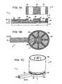
- FIG. 1A-1Crespectively illustrates side-sectional, top-sectional and perspective views of an exemplary coaxial transmission line microstructure in accordance with the invention
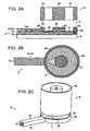
- FIG. 2A-2Crespectively illustrates side-sectional, top-sectional and perspective views of an exemplary coaxial transmission line microstructure in accordance with a further aspect of the invention
- FIG. 3A-3Brespectively illustrates side- and top-sectional views of an exemplary coaxial transmission line microstructure in accordance with a further aspect of the invention
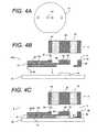
- FIG. 4A-4Cillustrates the joining to a substrate of an exemplary released coaxial transmission line microstructure in accordance with a further aspect of the invention
- FIG. 5A-5Cillustrates a frame for supporting a connectorized coaxial transmission line microstructure in accordance with a further aspect of the invention
- FIG. 6A-6Mrespectively illustrates side- and top-sectional views of an exemplary three-dimensional microstructure with transition structure at various stages of formation in accordance with the invention.
- FIG. 7illustrates a perspective view of an exemplary coaxial transmission line microstructure in accordance with a further aspect of the invention.
- FIGS. 8A-8Brespectively illustrates side- and perspective views of a stacked arrangement of the exemplary coaxial transmission line microstructure illustrated in FIG. 7 .
- microstructurerefers to structures formed by microfabrication processes, typically on a wafer or grid-level.
- sequential build processes of the inventiona microstructure is formed by sequentially layering and processing various materials and in a predetermined manner.
- film formation, lithographic patterning, deposition, etching and other optional processessuch as planarization techniques, a flexible method to form a variety of three-dimensional microstructures is provided.
- the sequential build processis generally accomplished through processes including various combinations of: (a) metal, sacrificial material (e.g., photoresist) and dielectric coating processes; (b) surface planarization; (c) photolithography; and (d) etching or planarization or other removal processes.
- metale.g., sacrificial material
- surface planarizatione.g., photoresist
- photolithographye.g., photolithography
- etching or planarization or other removal processese.g., etching or planarization or other removal processes.
- plating techniquesare particularly useful, although other metal deposition techniques such as physical vapor deposition (PVD), screen printing and chemical vapor deposition (CVD) techniques may be used, the choice dependent on the dimensions of the coaxial structures, and the materials deployed.
- PVDphysical vapor deposition
- CVDchemical vapor deposition
- transition structuresfor allowing electric and/or electromagnetic connection between coaxial transmission line microstructures and external components.
- Such a structurefinds application, for example, in the telecommunications and data communications industry, in chip to chip and interchip interconnect and passive components, in radar systems, and in microwave and millimeter-wave devices and subsystems.
- microdevicessuch as in pressure sensors, rollover sensors, mass spectrometers, filters, microfluidic devices, heat sinks, hermetic packages, surgical instruments, blood pressure sensors, air flow sensors, hearing aid sensors, micromechanical sensors, image stabilizers, altitude sensors and autofocus sensors.
- the inventioncan be used as a general method for fabricating transitions between microstructural elements for transmission of electric and/or electromagnetic signals and power with external components through a connector, for example, a microwave connector.
- the exemplified coaxial transmission line microstructures and related waveguidesare useful for propagation of electromagnetic energy having a frequency, for example, of from several MHz to 200 GHz or more, including radio frequency waves, millimeter waves and microwaves.
- the described transmission linesfind further use in providing a simultaneous DC or lower frequency voltage, for example, in providing a bias to integrated or attached semiconductor devices.
- FIG. 1A-1Cillustrates side-sectional, top-sectional and perspective views, respectively, of an exemplary coaxial transmission line microstructure 2 with a transition structure 4 and electric and/or electromagnetic connector (hereafter, electrical connector or connector) 6 , for example illustrated at least in FIG. 1A and FIG. 1C in accordance with one aspect of the invention.
- the exemplified microstructure 2is formed by a sequential build process, and includes a substrate 8 ( FIG. 1A ), a center conductor 10 , an outer conductor 12 disposed around and coaxial with the center conductor and one or more dielectric support members 14 a , 14 b for supporting the center conductor, for example illustrated in an aspect of embodiments at least in FIG.
- the outer conductor 12includes a conductive base layer 16 forming a lower wall, plural conductive layers forming the sidewalls, and conductive layer 24 forming an upper wall of the outer conductor, for example illustrated in an aspect of embodiments at least in FIG. 1A and FIG. 1C .
- the conductive layers forming the lower wall 16 and upper wall 24may optionally be provided as part of a conductive substrate or a conductive layer on a substrate.
- the volume 26for example illustrated in an aspect of embodiments at least in FIG. 1A , between the center conductor and the outer conductor is a non-solid, for example, a gas such as air or sulfur hexafluoride, vacuous or a liquid.
- the non-solid volumemay be of a porous material such as a porous dielectric material formed, for example, from a dielectric material containing volatile porogens which may be removed with heating.
- the transition structure 4 of the microstructure 2provides a larger geometry and lends mechanical support to the microstructure allowing for coupling to an electrical connector 6 ( FIGS. 1A & 1C ) without damaging the microstructure.
- the transitionadditionally minimizes or eliminates unwanted signal reflection between the transmission line microstructure 2 and electrical connector 6 .
- standard off-the-shelf surface mountable connectorsmay be coupled to the microstructures of the invention.
- the connector 6has a coaxial conductor structure including a center conductor 28 and an outer conductor 30 .
- the illustrated connectorhas a uniform geometry throughout its height.
- the connectoris to be joined to the microstructure 2 at a first end 32 , for example illustrated in an aspect of embodiments at least in FIG.
- Suitable connectorsinclude, for example, surface mount technology (SMT) versions of connectors such as 1 mm, 2.4 mm, 3.5 mm, Subminature A (SMA), K (Anritsu Co.), W (Anritsu Co.), Gilbert Push-On (GPO) and GPPO (Corning Inc.) connectors, and other standard connectors such as those designed to mate to coplanar waveguides.
- SMTsurface mount technology
- the transition structure 4can take various forms. Persons skilled in the art, given the exemplary structures and description herein, will understand that other designs may be employed. As shown, both the center conductor 10 and outer conductor 12 have an increased dimension at respective end portions 36 , 38 so as to be complementary in geometry to the center conductor 28 and outer conductor 30 of the electrical connector with which connection is to be made. For the center conductor, this increase in dimension is typically in the form of an increase in width, achieved by tapering the end portion of the center conductor from that of the transmission line standard width to that of the connector center conductor 28 . In this case, the exemplified center conductor end portion 36 also has an increase in the height dimension such that its height is the same as the outer conductor in the transition structure for purposes of bonding to the connector.
- solder layers 39may be disposed on the center and outer conductor in the transition structure to allow bonding with the connector.
- the height of the center conductor mating surface 40is equal to that of the mating surface 42 of the outer conductor in the transition region.
- the upper wall 24 of the outer conductor transition structureis open, thereby exposing the center conductor end portion 36 .
- the center conductoris suspended in the transition structure with a support structure.
- the load of the transmission line in the transition structurecan be significantly greater than that in other regions of the transmission line.
- the design of a suitable support structure for the center conductor end portion 36will generally differ from that of the dielectric support members 14 a used in the main regions of the transmission line.
- the design of the support structure for the end portion 36may take various forms and will depend on the mechanical loads and stresses as a result of its mass and environment, as well as the added mechanical forces it may be subject to as a result of the attachment and use of the connector structure, particularly those associated with the center conductor 28 .
- the support structure for the end portiontakes the form of plural dielectric support members 14 b , which may be in the form of straps as illustrated in FIGS. 1B & 1C .
- the dielectric support members 14 b as illustratedextend across the diameter of the outer conductor in the transition structure and are arranged in a spoke pattern.
- the dielectric support members 14 bare embedded in the outer conductor 38 . While the dielectric support members as illustrated extend below the center conductor end portion 36 , it should be clear that they may be embedded in the end portion 36 .
- FIG. 2A-2CA further design for a suitable support structure for the center conductor end portion 36 is illustrated in FIG. 2A-2C , which respectively shows side-sectional, top-sectional and perspective views of a further exemplary coaxial transmission line microstructure. Except as otherwise described, the description with respect to the exemplary structures of FIG. 1A-1C is generally applicable to the structures shown in FIG. 2A and FIG. 2C , as well as the additional exemplary structures to be described.
- the support structuretakes the form of a dielectric sheet 41 which supports the end portion 36 from below. As shown, the dielectric sheet 41 can be disposed across the entire transition structure or, alternatively, over a portion thereof.
- FIGS. 3A-3Brespectively illustrates side- and top-sectional views of such an exemplary support structure which includes a support pedestal 43 disposed below and in supporting contact with the center conductor end portion.
- the pedestalis formed at least in part from a dielectric material layer 44 so as to electrically isolate the center conductor from the outer conductor and substrate.
- An advantage of this pedestal-type support structure over the previously described embodimentsis its ability to withstand greater forces during connection with the connector and in normal use.
- the support structureincludes a dielectric material 44 , for example illustrated in an aspect of embodiments at least in FIG.
- the exemplified structureincludes a dielectric layer 44 such as a silicon nitride or silicon oxide layer on the surface of substrate 8 , for example illustrated in an aspect of embodiments at least in FIG. 3A .
- An opening 46 in the base layer 16 of the outer conductormay be provided in the transition structure to reduce capacitive coupling of the center and outer conductors.
- the pedestal 43is built up to a height such that the center conductor end portion 36 is directly supported thereby.
- the pedestalmay include one or more additional layers of the same or a different material, including dielectric and/or conductive materials.
- a conductive layer 47for example illustrated in an aspect of embodiments at least in FIG. 3A , of the same material as the outer conductor is provided over the dielectric layer 44 .
- the coaxial transmission line microstructuremay be released from the substrate on which it is formed.
- the released microstructure 48for example illustrated in an aspect of embodiments at least in FIG. 4B , may be joined to a separate substrate 50 on which is provided one or more support pedestals 43 for supporting the center conductor end portion 36 , for example illustrated in an aspect of embodiments at least in FIG. 4B , of the released microstructure.
- the connector 6for example illustrated in an aspect of embodiments at least in FIG. 4B , may then be connected to the pedestal-supported microstructure.
- the support pedestals 43may take the form, for example, of a printed circuit board, a ceramic, or a semiconductor, such as silicon, the post being formed on or as a part of the surface of the substrate 50 which itself may be of the same material.
- the pedestal 43may be formed by machining or etching the substrate 50 surface.
- the support pedestalmay be formed from a dielectric material, for example, a photoimageable dielectric material such as photosensitive-benzocyclobutene (Photo-BCB) resins such as those sold under the tradename Cyclotene (Dow Chemical Co.) and SU-8 resist (MicroChem. Corp.).
- the support pedestals 43may be formed and adhered to the released structure 48 rather than formed on the substrate 50 .
- the exemplary connector frame 52includes a rigid, durable member 54 , for example illustrated in an aspect of embodiments at least in FIG. 5A and FIG. 5C , constructed of, for example, a metal or metal alloy such as aluminum, stainless steel or a zinc alloy, or a dielectric material such as a ceramic material, for example, aluminum nitride or alumina, or a plastic.
- a metal or metal alloysuch as aluminum, stainless steel or a zinc alloy
- a dielectric materialsuch as a ceramic material, for example, aluminum nitride or alumina, or a plastic.
- the member 54has one or more apertures 56 , for example illustrated in an aspect of embodiments at least in FIG. 5A , extending therethrough having a geometry complementary to the connectors 6 , for example illustrated in an aspect of embodiments at least in FIG. 5C , such that the outside diameter of the connectors fit within the apertures.
- the connectorsmay be fixed in place by pressure fit and/or preferably by use of an appropriate adhesive or solder around the external surface of the connector.
- the frame 52provides a rigid structure to facilitate handling and connection and mating of cables or other hardware to the connectors attached in the frame that are mated to the microstructures 2 as shown in FIG. 5C . Thus, connection can easily be conducted by handling the frame instead of the individual connectors.
- the framemay further include a ring-, rectangular- or other-shaped structure 57 , for example illustrated in an aspect of embodiments at least in FIG. 5A and FIG. 5C , complementary in shape to the substrate 8 , for example illustrated in an aspect of embodiments at least in FIG. 5C , if any, on which the microstructures are disposed.
- the ring-shaped structuremay include a recess as shown by the dashed line for receiving the microstructure support or substrate.
- the componentsmay, for example, include a metal structural support in which they are embedded, for example, a released metal layer from the original substrate which may also form the bottom wall of the outer conductor or a metal open honeycomb structure.
- Such structurescan be formed at the same time and using the same process as used to make the micro-coaxial and/or waveguiding structures shown in the build sequence discussed with reference to FIGS. 6A-6M , where such an open structure is used to fill empty regions between the various coaxial members.
- the framemay optionally include a similar ring-shaped structure 59 , for example illustrated in an aspect of embodiments at least in FIG. 5B , with or without connectors, over the reverse surface of the microstructure substrate in a clam-shell configuration.
- Such a structurewould be useful to provide support for the center conductor as shown in FIGS. 3A-3B and FIGS. 4A-4C for those cases where the coaxial microstructures are released from their substrate. Release from the substrate is particularly useful where devices such as antennae and connectors are disposed and/or formed on opposite sides of the coaxial microstructures.
- the transmission lineis formed on a substrate 8 as shown in FIG. 6A , which may take various forms.
- the substratemay, for example, be constructed of a ceramic, a dielectric such as aluminum nitride, a semiconductor such as silicon, silicon-germanium or gallium arsenide, a metal such as copper or stainless steel, a polymer or a combination thereof.
- the substratecan take the form, for example, of an electronic substrate such as a printed wiring board or a semiconductor substrate, such as a silicon, silicon germanium, or gallium arsenide wafer. Such substrate wafers may contain active devices and/or other electronics elements.
- the substratemay be selected to have an expansion coefficient similar to the materials used in forming the transmission line, and should be selected so as to maintain its integrity during formation of the transmission line.
- the surface of the substrate on which the transmission line is to be formedis typically substantially planar.
- the substrate surfacemay, for example, be ground, lapped and/or polished to achieve a high degree of planarity.
- a conductive sacrificial layermay be deposited on the substrate. This can, for example, be a vapor deposited seed layer such as chrome and gold. Any of the methods of depositing conductive base layers for subsequent electroplating can be used.
- a first layer 60 a of a sacrificial photosensitive materialfor example, a photoresist, may next be deposited over the substrate 8 , and is exposed and developed to form a pattern 62 for subsequent deposition of the bottom wall of the transmission line outer conductor in both the transmission line main region and transition structure.
- the pattern 62includes a channel in the sacrificial material, exposing the top surface of the substrate 8 . Conventional photolithography steps and materials can be used for this purpose.
- the sacrificial photosensitive materialcan be, for example, a negative photoresist such as Shipley BPRTM 100 or PHOTOPOSITTM SN, and LAMINARTM dry films, commercially available from Rohm and Haas Electronic Materials LLC. Particularly suitable photosensitive materials are described in U.S. Pat. No. 6,054,252.
- Suitable binders for the sacrificial photosensitive materialinclude, for example: binder polymers prepared by free radical polymerization of acrylic acid and/or methacrylic acid with one or more monomers chosen from acrylate monomers, methacrylate monomers and vinyl aromatic monomers (acrylate polymers); acrylate polymers esterified with alcohols bearing (meth)acrylic groups, such as 2-hydroxyethyl(meth)acrylate, SB495B (Sartomer), Tone M-100 (Dow Chemical) or Tone M-210 (Dow Chemical); copolymers of styrene and maleic anhydride which have been converted to the half ester by reaction with an alcohol; copolymers of styrene and maleic anhydride which have been converted to the half ester by reaction with alcohols bearing (meth)acrylic groups, such as 2-hydroxyethyl methacrylate, SB495B (Sartomer), Tone M-100 (Dow Chemical) or Tone M-210 (Dow Chemical
- binder polymersinclude: copolymers of butyl acrylate, methyl methacrylate and methacrylic acid and copolymers of ethyl acrylate, methyl methacrylate and methacrylic acid; copolymers of butyl acrylate, methyl methacrylate and methacrylic acid and copolymers of ethyl acrylate, methyl methacrylate and methacrylic acid esterified with alcohols bearing methacrylic groups, such as 2-hydroxyethyl(meth)acrylate, SB495B (Sartomer), Tone M-100 (Dow Chemical) or Tone M-210 (Dow Chemical); copolymers of styrene and maleic anhydride such as SMA 1000F or SMA 3000F (Sartomer) that have been converted to the half ester by reaction with alcohols such as 2-hydroxyethyl methacrylate, SB495B (Sartomer), Tone M-100 (Dow Chemical) or Ton
- Suitable photoinitiator systems for the sacrificial photosensitive compositionsinclude Irgacure 184, Duracur 1173, Irgacure 651, Irgacure 907, Duracur ITX (all of Ciba Specialty Chemicals) and combinations thereof.
- the photosensitive compositionsmay include additional components, such as dyes, for example, methylene blue, leuco crystal violet, or Oil Blue N; additives to improve adhesion such as benzotriazole, benzimidazole, or benzoxizole; and surfactants such as Fluorad® FC-4430 (3M), Silwet L-7604 (GE), and Zonyl FSG (DuPont).
- the thickness of the sacrificial photosensitive material layers in this and other stepswill depend on the dimensions of the structures being fabricated, but are typically from 1 to 250 microns per layer, and in the case of the embodiments shown are more typically from 20 to 100 microns per strata or layer.
- TMAH developerssuch as the MicropositTM family of developers (Rohm and Haas Electronic Materials) such as Microposit MF-312, MF-26A, MF-321, MF-326W and MF-CD26 developers.
- a conductive base layer 16is formed over the substrate 8 and forms a lower wall of the outer conductor in the final structure for both the transmission line main region and transition structure.
- the base layer 16is typically formed of a material having high conductivity, such as a metal or metal-alloy (collectively referred to as “metal”), for example copper, silver, nickel, iron, aluminum, chromium, gold, titanium, alloys thereof, a doped semiconductor material, or combinations thereof, for example, multiple layers and/or multiple coatings of such materials in various combinations.
- metalmetal or metal-alloy
- the base layermay be deposited by a conventional process, for example, by plating such as electrolytic or electroless, or immersion plating, physical vapor deposition (PVD) such as sputtering or evaporation, or chemical vapor deposition (CVD).
- Plated coppermay, for example, be particularly suitable as the base layer material, with such techniques being well understood in the art.
- the platingcan be, for example, an electroless process using a copper salt and a reducing agent. Suitable materials are commercially available and include, for example, CIRCUPOSITTM electroless copper, available from Rohm and Haas Electronic Materials LLC, Marlborough, Mass. Alternatively, the material can be plated by coating an electrically conductive seed layer on top of or below the photoresist.
- the seed layermay be deposited by PVD over the substrate prior to coating of the sacrificial material, for example a first layer 60 a of a sacrificial photosensitive material.
- the use of an activated catalyst followed by electroless and/or electrolytic depositionmay be used.
- the base layer (and subsequent layers)may be patterned into arbitrary geometries to realize a desired device structure through the methods outlined.
- the thickness of the base layer 16is selected to provide mechanical stability to the microstructure and to provide sufficient conductivity of the transmission line to provide sufficiently low loss. At microwave frequencies and beyond, structural influences become more pronounced, as the skin depth will typically be less than 1 ⁇ m. The thickness thus will depend, for example, on the specific base layer material, the particular frequency to be propagated and the intended application. In instances in which the final structure is to be removed from the substrate, it may be beneficial to employ a relatively thick base layer, for example, from about 20 to 150 ⁇ m or from 20 to 80 ⁇ m, for structural integrity. Where the final structure is to remain intact with the substrate, it may be desired to employ a relatively thin base layer which may be determined by the skin depth requirements of the frequencies used.
- a material with suitable mechanical propertiesmay be chosen for the structure, and then it can be overcoated with a highly conductive material for its electrical properties.
- nickel base structurescan be overcoated with gold or silver using an electrolytic or more typically an electroless plating process.
- the base structuremay be overcoated with materials for other desired surface properties.
- coppermay be overcoated with electroless nickel and gold, or electroless silver, to help prevent oxidation.
- Other methods and materials for overcoatingmay be employed as are known in the art to obtain, for example, one or more of the target mechanical, chemical, electrical and corrosion-protective properties.
- Appropriate materials and techniques for forming the sidewallsare the same as those mentioned above with respect to the base layer.
- the sidewallsare typically formed of the same material used in forming the base layer 16 , although different materials may be employed.
- the application of a seed layer or plating basemay be omitted as here when metal in a subsequent step will only be applied directly over a previously formed, exposed metal region. It should be clear, however, that the exemplified structures shown in the figures typically make up only a small area of a particular device, and metallization of these and other structures may be started on any layer in the process sequence, in which case seed layers are typically used.
- CMPchemical-mechanical-polishing
- lappingor a combination of these methods are typically used.
- Other known planarization or mechanical forming techniquesfor example, mechanical finishing such as mechanical machining, diamond turning, plasma etching, laser ablation, and the like, may additionally or alternatively be used.
- CMP processcan be used to planarize the metal and the sacrificial material to the same level. This may be followed, for example, by a lapping process, which slowly removes metal, sacrificial material, and any dielectric at the same rate, allowing for greater control of the final thickness of the layer.
- a second layer 60 b of the sacrificial photosensitive materialis deposited over the base layer 16 and first sacrificial layer 60 a , and is exposed and developed to form a pattern 64 for subsequent deposition of lower sidewall portions of the transmission line outer conductor in the transmission line main region and transition structure.
- the pattern 64includes a channel exposing the top surface of the base layer 16 where the outer conductor sidewalls are to be formed.
- lower sidewall portions 18 of the transmission line outer conductor for the transmission line main region and transition structureare next formed.
- Appropriate materials and techniques for forming the sidewallsare the same as those mentioned above with respect to the base layer 16 although different materials may be employed.
- the application of a seed layer or plating basemay be omitted as here when metal in a subsequent step will only be applied directly over a previously formed, exposed metal region. Surface planarization as described above may be conducted at this stage.
- a layer 14 of a dielectric materialis next deposited over the second sacrificial layer 60 b and the lower sidewall portions 18 , as shown in FIG. 6E .
- support structuresare patterned from the dielectric layer to support the transmission line's center conductor to be formed in both the main region and the transition structure.
- the dielectric support layer 14should be formed from a material which will not create excessive losses for the signals to be transmitted through the transmission line.
- the materialshould also be capable of providing the mechanical strength necessary to support the center conductor along its length, including the end region in the transition structure.
- the materialshould further be relatively insoluble in the solvent used to remove the sacrificial material from the final transmission line structure.
- the materialis typically a dielectric material selected from photosensitive-benzocyclobutene (Photo-BCB) resins such as those sold under the tradename Cyclotene (Dow Chemical Co.), SU-8 resist (MicroChem. Corp.), inorganic materials, such as silicas and silicon oxides, SOL gels, various glasses, silicon nitride (Si 3 N 4 ), aluminum oxides such as alumina (Al 2 O 3 ), aluminum nitride (AlN), and magnesium oxide (MgO); organic materials such as polyethylene, polyester, polycarbonate, cellulose acetate, polypropylene, polyvinyl chloride, polyvinylidene chloride, polystyrene, polyamide, and polyimide; organic-inorganic hybrid materials such as organic silsesquioxane materials; a photodefinable dielectric such as a negative acting photoresist or photoepoxy which is not attacked by the sacrificial material removal process to be conducted.
- combinations of these materialsincluding composites and nano-composites of inorganic materials such as silica powders that are loaded into polymer materials may be used, for example to improve mechanical or chemical properties.
- SU-8 2015 resistis typical. It is advantageous to use materials which can be easily deposited, for example, by spin-coating, roller coating, squeegee coating, spray coating, chemical vapor deposition (CVD) or lamination.
- the dielectric material layer 14is deposited to a thickness that provides for the requisite support of the center conductor without cracking or breakage. In addition, the thickness should not severely impact subsequent application of sacrificial material layers from the standpoint of planarity. While the thickness of the dielectric support layer will depend on the dimensions and materials of the other elements of the microstructure, the thickness is typically from 1 to 100 microns, for example, about 20 microns.
- the dielectric material layer 14( FIG. 6E ) is next patterned using standard photolithography and developing techniques in the case of a photoimageable material to provide one or more first dielectric support members 14 a for supporting the center conductor in the main region of the transmission line and second dielectric support members 14 b in the transition structure.
- the dielectric support members 14 aextend from a first side of the outer conductor to an opposite side of the outer conductor.
- the dielectric support membersmay extend from the outer conductor and terminate at the center conductor.
- each of the support members 14 ais formed over one or the other lower sidewall portion 18 and the opposite end extends to a position over the sacrificial layer 60 b between the lower sidewall portions.
- the support members 14 aare spaced apart from one another, typically at a fixed distance.
- the number, shape, and pattern of arrangement of the dielectric support members 14 ashould be sufficient to provide support to the center conductor while also preventing excessive signal loss and dispersion.
- the dielectric support members 14 a and 14 bmay be patterned with geometries allowing for the elements of the microstructure to be maintained in mechanically locked engagement with each other, reducing the possibility of their pulling away from the outer conductor.
- the dielectric support members 14 aare patterned in the form of a “T” shape at each end (or an “I” shape) during the patterning process.
- such a structuremay optionally be used for the transition dielectric support members 14 b .
- the top portions 66 of the T structuresbecome embedded in the wall of the outer conductor and function to anchor the support members therein, rendering them more resistant to separation from the outer conductor.
- the illustrated structureincludes an anchor-type locking structure at each end of the dielectric support members 14 a , it should be clear that such a structure may be used at a single end thereof.
- the dielectric support membersmay optionally include an anchor portion on a single end in an alternating pattern. Reentrant profiles and other geometries providing an increase in cross-sectional geometry in the depthwise direction are typical.
- open structures, such as vias, in the central region of the dielectric patternmay be used to allow mechanical interlocking with subsequent metal regions to be formed.
- a third sacrificial photosensitive layer 60 cis coated over the substrate, and is exposed and developed to form patterns 68 , 70 for formation of middle sidewall portions of the transmission line outer conductor and the center conductor in the transition line main region and transition structure.
- the pattern 68 for the middle sidewall portionis coextensive with the lower sidewall portions 18 .
- the lower sidewall portions 18 and the end of the dielectric support members 14 a , 14 b overlying the lower sidewall portionsare exposed by pattern 68 .
- the pattern 70 for the center conductoris a channel along the length of the microstructure which tapers out at the transition structure.
- the pattern 70exposes supporting portions of the center conductor support members 14 a and 14 b .
- Conventional photolithography techniques and materials, such as those described above,can be used for this purpose.
- the center conductor 10 and middle sidewall portions 20 of the outer conductorare formed by depositing a suitable metal material into the channels formed in the third sacrificial material layer 60 c .
- a suitable metal materialfor forming the middle sidewall portions and center conductor are the same as those mentioned above with respect to the base layer 16 and lower sidewall portions 18 , although different materials and/or techniques may be employed.
- Surface planarizationmay optionally be performed at this stage to remove any unwanted metal deposited on the top surface of the sacrificial material in addition to providing a flat surface for subsequent processing, as has been previously described and optionally applied at any stage.
- a fourth sacrificial material layer 60 dis deposited over the substrate, and is exposed and developed to form pattern 72 for subsequent deposition of upper sidewall portions of the outer conductor for the transmission line main region and transition structure.
- the pattern 72 for the upper sidewall portionincludes a channel coextensive with and exposing the middle sidewall portion 20 .
- pattern 74is formed for subsequent deposition of a conductive layer on that portion of the center conductor end portion which is to be joined to the electrical connector.
- Such conductive layerallows for a coplanar center and outer conductor contact surface in the transition structure. Conventional photolithography steps and materials as described above can be used for this purpose.
- upper sidewall portions 22 of the outer conductor in the transmission line main region and transition structure, and an additional layer 76 on the center conductor end portion,are next formed by depositing a suitable material into the channels formed in the fourth sacrificial layer 60 d .
- a suitable materialfor forming these structures are the same as those mentioned above with respect to the base layer and other sidewall and center conductor portions.
- the upper sidewall portions 22 and center conductor end portion layer 76are typically formed with the same materials and techniques used in forming the base layer and other sidewalls and center conductor portions, although different materials and/or techniques may be employed. Surface planarization can optionally be performed at this stage to remove any unwanted metal deposited on the top surface of the sacrificial material in addition to providing a flat surface for subsequent processing.
- a fifth photosensitive sacrificial layer 60 eis deposited over the substrate, and is exposed and developed to form patterns 78 , 80 for subsequent deposition of the top wall of the transmission line outer conductor and a conductive layer on the previously formed layer of the center conductor end portion.
- the pattern 78 for the top wallexposes the upper sidewall portions 22 and the fourth sacrificial material layer 60 d therebetween.
- the pattern 80 for the center conductor end portionexposes the previously formed center conductor end portion layer 76 .
- openings in the outer conductor top wallfacilitating removal of the sacrificial material from the microstructure.
- openingsare represented as circles 82 , but may be squares, rectangles or other shapes. Further, while such openings are shown in the top layer, they may be included in any layer to improve the flow of solution to aid in removal of the sacrificial material later in the process.
- the shape, size and locationsare chosen based on design principles that include maintaining the desired mechanical integrity, maintaining sufficiently low radiation and scattering losses for the intended frequencies of operation, based on where the electrical fields are the lowest if being designed for low loss propagation, which is typically the corners of the coaxial structure, and based on sufficient fluid flow to remove the sacrificial material
- the upper wall 24 of the outer conductoris next formed by depositing a suitable material into the exposed region over and between the upper sidewall portions 22 of the transmission line main region.
- a further conductive layer 84is formed on the end portion of the center conductor over layer 76 .
- These layersare formed by depositing a suitable material into the channels formed in the fifth sacrificial layer 60 e .
- Metallizationis prevented at least in the volume occupied by the sacrificial material regions 82 , for example illustrated in an aspect of embodiments at least in FIG. 6K .
- Appropriate materials and techniques for forming these conductive structuresare the same as those mentioned above with respect to the base layer and other sidewall and center conductor layers, although different materials and/or techniques may be employed. Surface planarization can optionally be performed at this stage.
- solderable layers 39may be formed on the bonding surfaces of the transition structure as shown in FIG. 1A .
- the solderable layermay be formed in the same manner described above for the other conductive layers, using a further patterned layer of the sacrificial material followed by metallization, or other metallization technique such as by vapor deposition of the solder and use of a lift-off resist or shadow mask or by use of selective deposition.
- the solderable layermay include, for example, an Au--Sn solder or other solder material. The thickness of the solderable layers will depend on the particular materials involved, as well as the dimensions of the microstructure and of the connector.
- additional layersmay be added, for example, to create additional transmission lines or waveguides that may be interconnected to the first exemplary layer.
- Other layerssuch as the solders may optionally be added.
- the sacrificial material remaining in the structuremay next be removed.
- the sacrificial materialmay be removed by known strippers based on the type of material used. Suitable strippers include, for example: commercial stripping solutions such as SurfacestripTM 406-1, SurfacestripTM.
- aqueous solutions of strong basessuch as sodium hydroxide, potassium hydroxide, or tetramethylammonium hydroxide
- aqueous solutions of strong bases containing ethanol or monoethanolamineaqueous solutions of strong bases containing ethanol or monoethanolamine and a strong solvent such as N-methylpyrrolidone or N,N-dimethylformamide
- aqueous solutions of tetramethylammonium hydroxide, N-methylpyrrolidone and monoethanolamine or ethanolaqueous solutions of strong bases such as sodium hydroxide, potassium hydroxide, or tetramethylammonium hydroxide
- strong basessuch as sodium hydroxide, potassium hydroxide, or tetramethylammonium hydroxide
- aqueous solutions of strong bases containing ethanol or monoethanolamineaqueous solutions of strong bases containing ethanol or monoethanolamine
- a strong solventsuch as N-methylpyrrolidone or N,N-dimethylformamide
- the stripperis brought into contact with the sacrificial material.
- the sacrificial materialmay be exposed at the end faces of the transmission line structure. Additional openings in the transmission line such as described above may be provided to facilitate contact between the stripper and sacrificial material throughout the structure.
- Other structures for allowing contact between the sacrificial material and stripperare envisioned.
- openingscan be formed in the transmission line sidewalls during the patterning process.
- the dimensions of these openingsmay be selected to minimize interference with, scattering or leakage of the guided wave.
- the dimensionscan, for example, be selected to be less than 1 ⁇ 8, 1/10 or 1/20 of the wavelength of the highest frequency used.
- the impact of such openingscan readily be calculated and can be optimized using software such as HFSS made by Ansoft, Inc.
- the final transmission line microstructure 2 after removal of the sacrificial resistis shown in FIG. 6M .
- the volume previously occupied by the sacrificial material in and within the outer walls of the transmission lineforms apertures 88 in the outer conductor and forms the transmission line core 26 .
- the core volumeis typically occupied by a gas such as air. It is envisioned that a gas having better dielectric properties than air, for example, sulfur hexafluoride, may be used in the core.
- a vacuumcan be created in the core, for example, when the structure forms part of a hermetic package. As a result, a reduction in absorption from water vapor that may otherwise adsorb to the surfaces of the transmission lines can be realized. It is further envisioned that a liquid can occupy the core volume 26 between the center conductor and outer conductor, for example for cooling.
- the connector 6may next be attached to the transition structure 4 .
- Such attachmentmay be conducted by aligning the center and outer conductor mating surfaces of the connector with the corresponding structures of the transition structure, and forming a solder joint by heating.
- a solder film or solder ballcan be applied to either or both of the connector and microstructure mating surfaces.
- a thin film soldersuch as Au—Sn (80:20) solder may be used to join the parts.
- a solder flow wick-stop layermay be applied to the microstructure surrounding the region where solder will be applied for attachment.
- An inner wetting layeris patterned on the nickel, for example, a gold layer.
- the gold layerallows the solder to wet to where it is patterned.
- the surrounding nickel filmwill, however, prevent the solder from flowing onto other regions of the microstructure due to the formation of nickel oxides.
- Other methods of stopping the solder from wickingmay be employed.
- formation of a surrounding dielectric ringsuch as a permanent photopolymer as described with reference to the dielectric support layer may be employed.
- Other methods to control the flow of solderare known in the art.
- Bonding of the connector to the transition structuremay optionally be conducted with the use of a conductive adhesive, for example, a silver-filled epoxy or nano-sized metal particle paste.
- Conductive adhesivesare also available as an anisotropic conductive film or paste, wherein the conductive particle film or paste conduct only in one direction. The direction is determined by, for example, application of pressure or a magnetic field. This approach allows an easier method to align the connector and the microstructure as overflow of the material into surrounding regions will not produce electrical shorting.
- the final transmission line microstructuremay be separated from the substrate to which it is attached. This may be done prior to or after attachment of the connector. Release of the transmission line microstructure would allow for coupling to another substrate, for example, a gallium arsenide die such as a monolithic microwave integrated circuits or other devices. Such release also allows structures such as connectors and antennae to be on opposite sides of the microstructure without the need to machine through a substrate material. As shown previously in FIG. 4A-4C , released microstructures 48 can be joined to a separate substrate 50 , for example illustrated in an aspect of embodiments at least in FIG. 4C , designed to provide additional support to the transition structure in the form of a pedestal.
- a released microstructure with connectorscan offer other advantages, such as smaller thickness profiles, application of the completed microstructure to separately made die or wafers of active devices, and connectorization of both opposing surfaces of the microstructure.
- Release of the structure from the substratemay be accomplished by various techniques, for example, by use of a sacrificial layer between the substrate and the base layer which can be removed upon completion of the structure in a suitable solvent or etchant that does not attack or is sufficiently selective to the structural materials chosen.
- Suitable materials for the sacrificial layerinclude, for example, photoresists, selectively etchable metals such as chrome or titanium, high temperature waxes, and various salts.
- the exemplified transmission linesinclude a center conductor formed over the dielectric support members 14 a , 14 b , it is envisioned that they can be disposed within the center conductor such as in a split center conductor using a geometry such as a plus (+)-shape, a T-shape or a box.
- the support members 14 amay be formed over the center conductor in addition or as an alternative to the underlying dielectric support members. Further, the support members 14 a , 14 b may take the form of a pedestal, providing support from any of the surrounding surfaces when placed between a center conductor and a surrounding surface.
- FIGS. 7 and 8 A- 8 Bshow alternative exemplary embodiments of the transmission line microstructure of the invention.
- the transition structure 4is interfaced to a microwave connector 6 on the same axis rather than perpendicular to each other.
- a similar low loss transition region from the coaxial transmission linethat includes transmission line center conductor 10 and outer conductor 12 ) dimensions up to the dimensions of the connector center conductor 28 can be made.
- the transition structureis designed to either stop in-line with and adjacent to the center conductor 28 of the connector, allowing a wedge bond or wire bond interface, or allowing a solder or conductive epoxy connection.
- the center conductor transition of the coaxial waveguidemay be formed into a mating structure to receive the connector's center conductor where it may be attached with solder or conductive adhesive.
- the outer conductor 30 of the connectoris held either in a housing such as a metal block, or may be housed directly in a structured sidewall of the microstructure using the same basic processes that form the coaxial waveguide microstructure.
- the outer conductor of the connectormay be attached using solder or conductive epoxy. It may also be retained by creating a clam-shell two piece construction that mechanically retains the connector in the housing. Other approaches known in the art may be used to attach and retain the in-line connector.
- the transmission lines of the inventiontypically are square in cross-section. Other shapes, however, are envisioned. For example, other rectangular transmission lines can be obtained in the same manner the square transmission lines are formed, except making the width and height of the transmission lines different.
- Rounded transmission linesfor example, circular or partially rounded transmission lines can be formed by use of gray-scale patterning. Such rounded transmission lines can, for example, be created through conventional lithography for vertical transitions and might be used to more readily interface with external micro-coaxial conductors, to make connector interfaces, etc.
- a plurality of transmission lines as described abovemay be formed in a stacked arrangement, FIGS. 8A-8B , with the understanding that the transition structure 4 would typically be disposed so that the connector structure 6 can make electrical contact with the transition structure 4 .
- the stacked arrangementcan be achieved by continuation of the sequential build process through each stack, or by preforming the transmission lines on individual substrates, separating transmission line structures from their respective substrates using a release layer, and stacking the structures. Such stacked structures can be joined by thin layers of solders or conductive adhesives. In theory, there is not a limit on the number of transmission lines that can be stacked using the process steps discussed herein.
- the number of layerswill be limited by the ability to manage the thicknesses and stresses and, if they are built monolithically, the resist removal associated with each additional layer. While coaxial waveguide microstructures have been shown in the exemplified devices, the structures such as hollow-core waveguides, antenna elements, cavities, and so forth can also be constructed using the described methods and may be interspersed with the connector shown.
- transmission line microstructuresshow a single transmission line and connector, it should be clear that a plurality of such transmission lines each to be joined to a plurality of connectors are typical. Further, such structures are typically manufactured on a wafer- or grid-level as a plurality of die.
- microstructures and methods of the inventionfind use, for example, in: microwave and millimeter wave active and passive components and subsystems, in microwave amplifiers, in satellite communications, in data and telecommunications such as point to point data links, in microwave and millimeter wave filters and couplers; in aerospace and military applications, in radar and collision avoidance systems, and communications systems; in automotive pressure and/or rollover sensors; chemistry in mass spectrometers and filters; biotechnology and biomedical in filters, in wafer or grid level electrical probing, in gyroscopes and accelerometers, in microfluidic devices, in surgical instruments and blood pressure sensing, in air flow and hearing aid sensors; and consumer electronics such as in image stabilizers, altitude sensors, and autofocus sensors.
Landscapes
- Engineering & Computer Science (AREA)
- Manufacturing & Machinery (AREA)
- Waveguides (AREA)
- Multi-Conductor Connections (AREA)
Abstract
Description
Claims (11)
Priority Applications (4)
| Application Number | Priority Date | Filing Date | Title |
|---|---|---|---|
| US14/029,252US9000863B2 (en) | 2007-03-20 | 2013-09-17 | Coaxial transmission line microstructure with a portion of increased transverse dimension and method of formation thereof |
| US14/680,345US9570789B2 (en) | 2007-03-20 | 2015-04-07 | Transition structure between a rectangular coaxial microstructure and a cylindrical coaxial cable using step changes in center conductors thereof |
| US15/405,799US10135109B2 (en) | 2007-03-20 | 2017-01-13 | Method of forming a coaxial line microstructure having an enlarged region on a substrate and removing the coaxial line microstructure from the substrate for mounting on a mounting substrate |
| US16/170,896US20190067790A1 (en) | 2007-03-20 | 2018-10-25 | Coaxial transmission line microstructures and methods of formation thereof |
Applications Claiming Priority (4)
| Application Number | Priority Date | Filing Date | Title |
|---|---|---|---|
| US91912407P | 2007-03-20 | 2007-03-20 | |
| US12/077,546US7898356B2 (en) | 2007-03-20 | 2008-03-20 | Coaxial transmission line microstructures and methods of formation thereof |
| US13/015,671US8542079B2 (en) | 2007-03-20 | 2011-01-28 | Coaxial transmission line microstructure including an enlarged coaxial structure for transitioning to an electrical connector |
| US14/029,252US9000863B2 (en) | 2007-03-20 | 2013-09-17 | Coaxial transmission line microstructure with a portion of increased transverse dimension and method of formation thereof |
Related Parent Applications (1)
| Application Number | Title | Priority Date | Filing Date |
|---|---|---|---|
| US13/015,671ContinuationUS8542079B2 (en) | 2007-03-20 | 2011-01-28 | Coaxial transmission line microstructure including an enlarged coaxial structure for transitioning to an electrical connector |
Related Child Applications (1)
| Application Number | Title | Priority Date | Filing Date |
|---|---|---|---|
| US14/680,345ContinuationUS9570789B2 (en) | 2007-03-20 | 2015-04-07 | Transition structure between a rectangular coaxial microstructure and a cylindrical coaxial cable using step changes in center conductors thereof |
Publications (2)
| Publication Number | Publication Date |
|---|---|
| US20140015623A1 US20140015623A1 (en) | 2014-01-16 |
| US9000863B2true US9000863B2 (en) | 2015-04-07 |
Family
ID=39563288
Family Applications (6)
| Application Number | Title | Priority Date | Filing Date |
|---|---|---|---|
| US12/077,546ActiveUS7898356B2 (en) | 2007-03-20 | 2008-03-20 | Coaxial transmission line microstructures and methods of formation thereof |
| US13/015,671ActiveUS8542079B2 (en) | 2007-03-20 | 2011-01-28 | Coaxial transmission line microstructure including an enlarged coaxial structure for transitioning to an electrical connector |
| US14/029,252ActiveUS9000863B2 (en) | 2007-03-20 | 2013-09-17 | Coaxial transmission line microstructure with a portion of increased transverse dimension and method of formation thereof |
| US14/680,345ActiveUS9570789B2 (en) | 2007-03-20 | 2015-04-07 | Transition structure between a rectangular coaxial microstructure and a cylindrical coaxial cable using step changes in center conductors thereof |
| US15/405,799Expired - Fee RelatedUS10135109B2 (en) | 2007-03-20 | 2017-01-13 | Method of forming a coaxial line microstructure having an enlarged region on a substrate and removing the coaxial line microstructure from the substrate for mounting on a mounting substrate |
| US16/170,896AbandonedUS20190067790A1 (en) | 2007-03-20 | 2018-10-25 | Coaxial transmission line microstructures and methods of formation thereof |
Family Applications Before (2)
| Application Number | Title | Priority Date | Filing Date |
|---|---|---|---|
| US12/077,546ActiveUS7898356B2 (en) | 2007-03-20 | 2008-03-20 | Coaxial transmission line microstructures and methods of formation thereof |
| US13/015,671ActiveUS8542079B2 (en) | 2007-03-20 | 2011-01-28 | Coaxial transmission line microstructure including an enlarged coaxial structure for transitioning to an electrical connector |
Family Applications After (3)
| Application Number | Title | Priority Date | Filing Date |
|---|---|---|---|
| US14/680,345ActiveUS9570789B2 (en) | 2007-03-20 | 2015-04-07 | Transition structure between a rectangular coaxial microstructure and a cylindrical coaxial cable using step changes in center conductors thereof |
| US15/405,799Expired - Fee RelatedUS10135109B2 (en) | 2007-03-20 | 2017-01-13 | Method of forming a coaxial line microstructure having an enlarged region on a substrate and removing the coaxial line microstructure from the substrate for mounting on a mounting substrate |
| US16/170,896AbandonedUS20190067790A1 (en) | 2007-03-20 | 2018-10-25 | Coaxial transmission line microstructures and methods of formation thereof |
Country Status (4)
| Country | Link |
|---|---|
| US (6) | US7898356B2 (en) |
| EP (1) | EP1973189B1 (en) |
| JP (1) | JP2009005335A (en) |
| KR (1) | KR101472134B1 (en) |
Cited By (16)
| Publication number | Priority date | Publication date | Assignee | Title |
|---|---|---|---|---|
| US20140327439A1 (en)* | 2013-05-01 | 2014-11-06 | Massachusetts Institute Of Technology | Stable three-axis nuclear spin gyroscope |
| US20160072171A1 (en)* | 2007-03-20 | 2016-03-10 | Nuvotronics, Llc | Coaxial transmission line microstructures and methods of formation thereof |
| US9505613B2 (en) | 2011-06-05 | 2016-11-29 | Nuvotronics, Inc. | Devices and methods for solder flow control in three-dimensional microstructures |
| US9515364B1 (en) | 2006-12-30 | 2016-12-06 | Nuvotronics, Inc. | Three-dimensional microstructure having a first dielectric element and a second multi-layer metal element configured to define a non-solid volume |
| US9583856B2 (en) | 2011-06-06 | 2017-02-28 | Nuvotronics, Inc. | Batch fabricated microconnectors |
| US9608303B2 (en) | 2013-01-26 | 2017-03-28 | Nuvotronics, Inc. | Multi-layer digital elliptic filter and method |
| US9888600B2 (en) | 2013-03-15 | 2018-02-06 | Nuvotronics, Inc | Substrate-free interconnected electronic mechanical structural systems |
| US10002818B2 (en) | 2007-03-20 | 2018-06-19 | Nuvotronics, Inc. | Integrated electronic components and methods of formation thereof |
| US10074885B2 (en) | 2003-03-04 | 2018-09-11 | Nuvotronics, Inc | Coaxial waveguide microstructures having conductors formed by plural conductive layers |
| US10158200B2 (en)* | 2016-11-28 | 2018-12-18 | Hirose Electric Co., Ltd. | Coaxial electrical connector and manufacturing method thereof |
| US10193203B2 (en) | 2013-03-15 | 2019-01-29 | Nuvotronics, Inc | Structures and methods for interconnects and associated alignment and assembly mechanisms for and between chips, components, and 3D systems |
| US10310009B2 (en) | 2014-01-17 | 2019-06-04 | Nuvotronics, Inc | Wafer scale test interface unit and contactors |
| US10319654B1 (en) | 2017-12-01 | 2019-06-11 | Cubic Corporation | Integrated chip scale packages |
| US10497511B2 (en) | 2009-11-23 | 2019-12-03 | Cubic Corporation | Multilayer build processes and devices thereof |
| US10511073B2 (en) | 2014-12-03 | 2019-12-17 | Cubic Corporation | Systems and methods for manufacturing stacked circuits and transmission lines |
| US10847469B2 (en) | 2016-04-26 | 2020-11-24 | Cubic Corporation | CTE compensation for wafer-level and chip-scale packages and assemblies |
Families Citing this family (59)
| Publication number | Priority date | Publication date | Assignee | Title |
|---|---|---|---|---|
| US9614266B2 (en)* | 2001-12-03 | 2017-04-04 | Microfabrica Inc. | Miniature RF and microwave components and methods for fabricating such components |
| TWI360912B (en)* | 2008-04-25 | 2012-03-21 | Univ Nat Chiao Tung | Vertical transition structure |
| US8659371B2 (en)* | 2009-03-03 | 2014-02-25 | Bae Systems Information And Electronic Systems Integration Inc. | Three-dimensional matrix structure for defining a coaxial transmission line channel |
| KR101917052B1 (en) | 2010-01-22 | 2019-01-30 | 누보트로닉스, 인크. | Thermal management |
| US8917150B2 (en) | 2010-01-22 | 2014-12-23 | Nuvotronics, Llc | Waveguide balun having waveguide structures disposed over a ground plane and having probes located in channels |
| US8597040B2 (en)* | 2010-03-03 | 2013-12-03 | Thomas & Betts International, Inc. | Device having an electrical connector and a sacrificial cap |
| US8616908B2 (en)* | 2010-03-03 | 2013-12-31 | Thomas & Betts International, Inc. | Electrical connector with a cap with a sacrificial conductor |
| US8172596B2 (en)* | 2010-03-03 | 2012-05-08 | Thomas & Betts International, Inc. | Electrical connector with sacrificial appendage |
| DE102010019447A1 (en)* | 2010-05-05 | 2011-11-10 | Eos Gmbh Electro Optical Systems | A method for generatively producing a three-dimensional object with reamers and method for creating a corresponding dataset |
| KR101902558B1 (en) | 2010-07-02 | 2018-10-01 | 누보트로닉스, 인크. | Three-dimensional microstructures |
| JP5248578B2 (en)* | 2010-11-19 | 2013-07-31 | 株式会社東芝 | Coaxial connector, substrate having coaxial connector, method of manufacturing substrate having coaxial connector, and coaxial connector assembly |
| US9200883B2 (en)* | 2011-05-05 | 2015-12-01 | International Business Machines Corporation | Transferable probe tips |
| WO2013010108A1 (en) | 2011-07-13 | 2013-01-17 | Nuvotronics, Llc | Methods of fabricating electronic and mechanical structures |
| US9142497B2 (en) | 2011-10-05 | 2015-09-22 | Harris Corporation | Method for making electrical structure with air dielectric and related electrical structures |
| US9065163B1 (en) | 2011-12-23 | 2015-06-23 | Nuvotronics, Llc | High frequency power combiner/divider |
| CN103733427B (en)* | 2012-02-03 | 2015-08-26 | 株式会社村田制作所 | High frequency signal transmission line and electronic equipment |
| GB2512982B (en)* | 2012-02-03 | 2018-06-13 | Murata Manufacturing Co | High-frequency signal transmission line and electronic device |
| US8952770B2 (en)* | 2012-06-21 | 2015-02-10 | Oml, Inc. | Self keying and orientation system for a repeatable waveguide calibration and connection |
| US20140055215A1 (en) | 2012-08-23 | 2014-02-27 | Harris Corporation | Distributed element filters for ultra-broadband communications |
| WO2014031920A1 (en) | 2012-08-23 | 2014-02-27 | Harris Corporation | Switches for use in microelectromechanical and other systems, and processes for making same |
| US9165723B2 (en)* | 2012-08-23 | 2015-10-20 | Harris Corporation | Switches for use in microelectromechanical and other systems, and processes for making same |
| US9053874B2 (en) | 2012-09-20 | 2015-06-09 | Harris Corporation | MEMS switches and other miniaturized devices having encapsulating enclosures, and processes for fabricating same |
| US9053873B2 (en) | 2012-09-20 | 2015-06-09 | Harris Corporation | Switches for use in microelectromechanical and other systems, and processes for making same |
| US8907849B2 (en) | 2012-10-12 | 2014-12-09 | Harris Corporation | Wafer-level RF transmission and radiation devices |
| US9203133B2 (en) | 2012-10-18 | 2015-12-01 | Harris Corporation | Directional couplers with variable frequency response |
| US9090459B2 (en) | 2012-11-30 | 2015-07-28 | Harris Corporation | Control circuitry routing configuration for MEMS devices |
| US9148111B2 (en) | 2012-11-30 | 2015-09-29 | Harris Corporation | Phase shifters and tuning elements |
| US9185820B2 (en) | 2012-12-11 | 2015-11-10 | Harris Corporation | Monolithically integrated RF system and method of making same |
| US8952752B1 (en) | 2012-12-12 | 2015-02-10 | Nuvotronics, Llc | Smart power combiner |
| US9660336B2 (en)* | 2013-02-07 | 2017-05-23 | Kevan ANDERSON | Systems, devices and methods for transmitting electrical signals through a faraday cage |
| JP5967290B2 (en)* | 2013-07-09 | 2016-08-10 | 株式会社村田製作所 | High frequency transmission line |
| US9281624B2 (en) | 2013-08-16 | 2016-03-08 | Tyco Electronics Corporation | Electrical connector with signal pathways and a system having the same |
| US9136822B2 (en) | 2013-08-19 | 2015-09-15 | Harris Corporation | Microelectromechanical system with a micro-scale spring suspension system and methods for making the same |
| US9172352B2 (en) | 2013-08-19 | 2015-10-27 | Harris Corporation | Integrated microelectromechanical system devices and methods for making the same |
| US9093975B2 (en) | 2013-08-19 | 2015-07-28 | Harris Corporation | Microelectromechanical systems comprising differential inductors and methods for making the same |
| CN104459855A (en)* | 2013-09-22 | 2015-03-25 | 清华大学 | Preparation method of metal grating |
| CN104459852B (en)* | 2013-09-22 | 2017-02-01 | 清华大学 | Preparation method of metal grating |
| CN104459854B (en)* | 2013-09-22 | 2017-12-01 | 清华大学 | The preparation method of metal grating |
| US9123493B2 (en) | 2014-01-23 | 2015-09-01 | Harris Corporation | Microelectromechanical switches for steering of RF signals |
| US9123738B1 (en) | 2014-05-16 | 2015-09-01 | Xilinx, Inc. | Transmission line via structure |
| US9972880B2 (en) | 2014-07-16 | 2018-05-15 | Keysight Technologies, Inc. | Method for building a connection between a coaxial RF cable and hybrid package using 3D printing and a connection receptacle |
| US9478494B1 (en) | 2015-05-12 | 2016-10-25 | Harris Corporation | Digital data device interconnects |
| US9437911B1 (en)* | 2015-05-21 | 2016-09-06 | Harris Corporation | Compliant high speed interconnects |
| WO2017091903A1 (en) | 2015-12-03 | 2017-06-08 | Innovere Medical Inc. | Systems, devices and methods for wireless transmission of signals through a faraday cage |
| KR101962936B1 (en)* | 2016-03-24 | 2019-03-28 | (주)유니드 | Organic and inorganic composite thin film |
| JP7252630B2 (en) | 2017-05-09 | 2023-04-05 | イノベア メディカル インコーポレーテッド | Systems and devices for wireless communication through electromagnetically shielded windows |
| CN111033888B (en)* | 2017-07-11 | 2021-12-28 | 康普技术有限责任公司 | Device for power combining |
| US11426818B2 (en) | 2018-08-10 | 2022-08-30 | The Research Foundation for the State University | Additive manufacturing processes and additively manufactured products |
| US11257771B2 (en)* | 2019-01-02 | 2022-02-22 | Keysight Technologies, Inc. | High-performance integrated circuit packaging platform compatible with surface mount assembly |
| US11605583B2 (en) | 2019-01-02 | 2023-03-14 | Keysight Technologies, Inc. | High-performance integrated circuit packaging platform compatible with surface mount assembly |
| FR3092588B1 (en)* | 2019-02-11 | 2022-01-21 | Radiall Sa | Anti-multipactor coating deposited on an RF or MW metal component, Process for producing such a coating by laser texturing. |
| KR102321330B1 (en)* | 2019-05-31 | 2021-11-04 | 한국전자기술연구원 | Half coaxial transmission line, semiconductor package including the same, and manufacturing method thereof |
| DE102019115307A1 (en) | 2019-06-06 | 2020-12-10 | Infineon Technologies Ag | Semi-conductor devices with planar waveguide transmission lines |
| US11350520B2 (en)* | 2019-08-08 | 2022-05-31 | At&S Austria Technologie & Systemtechnik Aktiengesellschaft | Component carrier and method of manufacturing the same |
| CN110449332A (en)* | 2019-08-13 | 2019-11-15 | 上海金铎禹辰水环境工程有限公司 | A kind of composite construction diamond thin and preparation method thereof |
| US11367948B2 (en) | 2019-09-09 | 2022-06-21 | Cubic Corporation | Multi-element antenna conformed to a conical surface |
| US11456227B2 (en)* | 2019-12-17 | 2022-09-27 | Nxp Usa, Inc. | Topside heatsinking antenna launcher for an integrated circuit package |
| CN113540915A (en)* | 2021-07-19 | 2021-10-22 | 赛莱克斯微系统科技(北京)有限公司 | Micro-coaxial radio frequency transmission line and GSG (ground satellite System) adapter thereof |
| SE545405C2 (en)* | 2021-10-21 | 2023-08-01 | Gapwaves Ab | A coaxial transition arrangement |
Citations (149)
| Publication number | Priority date | Publication date | Assignee | Title |
|---|---|---|---|---|
| US2812501A (en) | 1954-03-04 | 1957-11-05 | Sanders Associates Inc | Transmission line |
| US2914766A (en) | 1955-06-06 | 1959-11-24 | Sanders Associates Inc | Three conductor planar antenna |
| US2997519A (en) | 1959-10-08 | 1961-08-22 | Bell Telephone Labor Inc | Multicoaxial line cables |
| US3309632A (en) | 1965-04-13 | 1967-03-14 | Kollmorgen Corp | Microwave contactless coaxial connector |
| US3311966A (en) | 1962-09-24 | 1967-04-04 | North American Aviation Inc | Method of fabricating multilayer printed-wiring boards |
| US3335489A (en) | 1962-09-24 | 1967-08-15 | North American Aviation Inc | Interconnecting circuits with a gallium and indium eutectic |
| US3352730A (en) | 1964-08-24 | 1967-11-14 | Sanders Associates Inc | Method of making multilayer circuit boards |
| US3464855A (en) | 1966-09-06 | 1969-09-02 | North American Rockwell | Process for forming interconnections in a multilayer circuit board |
| US3560896A (en) | 1967-07-06 | 1971-02-02 | Telefunken Patent | Inner conductor support for shielded microwave strip lines |
| FR2086327A1 (en) | 1970-04-24 | 1971-12-31 | Spinner Gmbh Elektrotech | |
| US3775844A (en) | 1970-06-25 | 1973-12-04 | Bunker Ramo | Method of fabricating a multiwafer electrical circuit structure |
| US3789129A (en) | 1972-06-06 | 1974-01-29 | Felten & Guilleaume Ag | Air-insulated coaxial high-frequency cable |
| US3791858A (en) | 1971-12-13 | 1974-02-12 | Ibm | Method of forming multi-layer circuit panels |
| US3963999A (en) | 1975-05-29 | 1976-06-15 | The Furukawa Electric Co., Ltd. | Ultra-high-frequency leaky coaxial cable |
| US4021789A (en) | 1975-09-29 | 1977-05-03 | International Business Machines Corporation | Self-aligned integrated circuits |
| US4075757A (en) | 1975-12-17 | 1978-02-28 | Perstorp Ab | Process in the production of a multilayer printed board |
| US4275944A (en) | 1979-07-09 | 1981-06-30 | Sochor Jerzy R | Miniature connector receptacles employing contacts with bowed tines and parallel mounting arms |
| US4348253A (en) | 1981-11-12 | 1982-09-07 | Rca Corporation | Method for fabricating via holes in a semiconductor wafer |
| US4365222A (en) | 1981-04-06 | 1982-12-21 | Bell Telephone Laboratories, Incorporated | Stripline support assembly |
| US4414424A (en) | 1980-10-20 | 1983-11-08 | Tokyo Shibaura Denki Kabushiki Kaisha | Gas-insulated bus bar |
| US4417393A (en) | 1981-04-01 | 1983-11-29 | General Electric Company | Method of fabricating high density electronic circuits having very narrow conductors |
| US4437074A (en) | 1980-12-18 | 1984-03-13 | Thomson-Csf | Ultrahigh-frequency transmission line of the three-plate air type and uses thereof |
| US4521755A (en) | 1982-06-14 | 1985-06-04 | At&T Bell Laboratories | Symmetrical low-loss suspended substrate stripline |
| US4581301A (en) | 1984-04-10 | 1986-04-08 | Michaelson Henry W | Additive adhesive based process for the manufacture of printed circuit boards |
| US4591411A (en) | 1982-05-05 | 1986-05-27 | Hughes Aircraft Company | Method for forming a high density printed wiring board |
| US4641140A (en) | 1983-09-26 | 1987-02-03 | Harris Corporation | Miniaturized microwave transmission link |
| US4663497A (en) | 1982-05-05 | 1987-05-05 | Hughes Aircraft Company | High density printed wiring board |
| US4673904A (en) | 1984-11-14 | 1987-06-16 | Itt Corporation | Micro-coaxial substrate |
| US4700159A (en) | 1985-03-29 | 1987-10-13 | Weinschel Engineering Co., Inc. | Support structure for coaxial transmission line using spaced dielectric balls |
| DE3623093A1 (en) | 1986-07-09 | 1988-01-21 | Standard Elektrik Lorenz Ag | Method for producing through-connections in printed circuit boards or multilayer printed circuit boards having inorganic or organic/inorganic insulating layers |
| US4771294A (en) | 1986-09-10 | 1988-09-13 | Harris Corporation | Modular interface for monolithic millimeter wave antenna array |
| US4808273A (en) | 1988-05-10 | 1989-02-28 | Avantek, Inc. | Method of forming completely metallized via holes in semiconductors |
| US4853656A (en) | 1987-08-03 | 1989-08-01 | Aerospatiale Societe Nationale Industrielle | Device for connecting together two ultra-high frequency structures which are coaxial and of different diameters |
| US4856184A (en) | 1988-06-06 | 1989-08-15 | Tektronix, Inc. | Method of fabricating a circuit board |
| US4857418A (en) | 1986-12-08 | 1989-08-15 | Honeywell Inc. | Resistive overlayer for magnetic films |
| US4876322A (en) | 1984-08-10 | 1989-10-24 | Siemens Aktiengesselschaft | Irradiation cross-linkable thermostable polymer system, for microelectronic applications |
| US4880684A (en) | 1988-03-11 | 1989-11-14 | International Business Machines Corporation | Sealing and stress relief layers and use thereof |
| JPH027587A (en) | 1988-06-27 | 1990-01-11 | Yokogawa Electric Corp | Variable frequency light source |
| US4969979A (en) | 1989-05-08 | 1990-11-13 | International Business Machines Corporation | Direct electroplating of through holes |
| US4975142A (en) | 1989-11-07 | 1990-12-04 | General Electric Company | Fabrication method for printed circuit board |
| US5069749A (en) | 1986-07-29 | 1991-12-03 | Digital Equipment Corporation | Method of fabricating interconnect layers on an integrated circuit chip using seed-grown conductors |
| US5072201A (en) | 1988-12-06 | 1991-12-10 | Thomson-Csf | Support for microwave transmission line, notably of the symmetrical strip line type |
| US5100501A (en) | 1989-06-30 | 1992-03-31 | Texas Instruments Incorporated | Process for selectively depositing a metal in vias and contacts by using a sacrificial layer |
| CA2055116A1 (en) | 1990-11-13 | 1992-05-14 | Jurg Buhler | Automatic analysis apparatus |
| US5119049A (en) | 1991-04-12 | 1992-06-02 | Ail Systems, Inc. | Ultraminiature low loss coaxial delay line |
| US5227013A (en) | 1991-07-25 | 1993-07-13 | Microelectronics And Computer Technology Corporation | Forming via holes in a multilevel substrate in a single step |
| JPH0685510A (en) | 1992-03-31 | 1994-03-25 | Yokogawa Electric Corp | Multi-chip module |
| US5334956A (en) | 1992-03-30 | 1994-08-02 | Motorola, Inc. | Coaxial cable having an impedance matched terminating end |
| US5381157A (en) | 1991-05-02 | 1995-01-10 | Sumitomo Electric Industries, Ltd. | Monolithic microwave integrated circuit receiving device having a space between antenna element and substrate |
| US5406423A (en) | 1990-10-01 | 1995-04-11 | Asahi Kogaku Kogyo Kabushiki Kaisha | Apparatus and method for retrieving audio signals from a recording medium |
| US5406235A (en) | 1990-12-26 | 1995-04-11 | Tdk Corporation | High frequency device |
| US5430257A (en) | 1992-08-12 | 1995-07-04 | Trw Inc. | Low stress waveguide window/feedthrough assembly |
| US5454161A (en) | 1993-04-29 | 1995-10-03 | Fujitsu Limited | Through hole interconnect substrate fabrication process |
| US5622895A (en) | 1994-05-09 | 1997-04-22 | Lucent Technologies Inc. | Metallization for polymer-dielectric multichip modules |
| US5633615A (en) | 1995-12-26 | 1997-05-27 | Hughes Electronics | Vertical right angle solderless interconnects from suspended stripline to three-wire lines on MIC substrates |
| US5682062A (en) | 1995-06-05 | 1997-10-28 | Harris Corporation | System for interconnecting stacked integrated circuits |
| US5682124A (en) | 1993-02-02 | 1997-10-28 | Ast Research, Inc. | Technique for increasing the range of impedances for circuit board transmission lines |
| US5712607A (en) | 1996-04-12 | 1998-01-27 | Dittmer; Timothy W. | Air-dielectric stripline |
| US5724012A (en) | 1994-02-03 | 1998-03-03 | Hollandse Signaalapparaten B.V. | Transmission-line network |
| US5746868A (en) | 1994-07-21 | 1998-05-05 | Fujitsu Limited | Method of manufacturing multilayer circuit substrate |
| US5793272A (en) | 1996-08-23 | 1998-08-11 | International Business Machines Corporation | Integrated circuit toroidal inductor |
| US5814889A (en) | 1995-06-05 | 1998-09-29 | Harris Corporation | Intergrated circuit with coaxial isolation and method |
| US5860812A (en) | 1997-01-23 | 1999-01-19 | Litton Systems, Inc. | One piece molded RF/microwave coaxial connector |
| US5872399A (en) | 1996-04-01 | 1999-02-16 | Anam Semiconductor, Inc. | Solder ball land metal structure of ball grid semiconductor package |
| US5925206A (en) | 1997-04-21 | 1999-07-20 | International Business Machines Corporation | Practical method to make blind vias in circuit boards and other substrates |
| US5961347A (en) | 1996-09-26 | 1999-10-05 | Hon Hai Precision Ind. Co., Ltd. | Micro connector |
| US5977842A (en) | 1998-07-01 | 1999-11-02 | Raytheon Company | High power broadband coaxial balun |
| US5990768A (en) | 1996-11-28 | 1999-11-23 | Matsushita Electric Industrial Co., Ltd. | Millimeter waveguide and a circuit apparatus using the same |
| US6008102A (en) | 1998-04-09 | 1999-12-28 | Motorola, Inc. | Method of forming a three-dimensional integrated inductor |
| US6027630A (en) | 1997-04-04 | 2000-02-22 | University Of Southern California | Method for electrochemical fabrication |
| JP3027587B2 (en) | 1989-11-07 | 2000-04-04 | 株式会社リコー | Facsimile machine |
| US6054252A (en) | 1998-12-11 | 2000-04-25 | Morton International, Inc. | Photoimageable compositions having improved chemical resistance and stripping ability |
| WO2000007218A3 (en) | 1998-07-28 | 2000-05-04 | Korea Advanced Inst Sci & Tech | Method for manufacturing a semiconductor device having a metal layer floating over a substrate |
| WO2000039854A1 (en) | 1998-12-28 | 2000-07-06 | Telephus, Inc. | Coaxial type signal line and manufacturing method thereof |
| US6180261B1 (en) | 1997-10-21 | 2001-01-30 | Nitto Denko Corporation | Low thermal expansion circuit board and multilayer wiring circuit board |
| US6210221B1 (en) | 1999-10-13 | 2001-04-03 | Maury Microwave, Inc. | Microwave quick connect/disconnect coaxial connectors |
| US6228466B1 (en) | 1997-04-11 | 2001-05-08 | Ibiden Co. Ltd. | Printed wiring board and method for manufacturing the same |
| EP0911903A3 (en) | 1997-10-22 | 2001-06-06 | Nokia Mobile Phones Ltd. | Coaxcial cable, method for manufacturing a coaxial cable, and wireless communication device |
| US6294965B1 (en) | 1999-03-11 | 2001-09-25 | Anaren Microwave, Inc. | Stripline balun |
| US6350633B1 (en) | 2000-08-22 | 2002-02-26 | Charles W. C. Lin | Semiconductor chip assembly with simultaneously electroplated contact terminal and connection joint |
| US6388198B1 (en) | 1999-03-09 | 2002-05-14 | International Business Machines Corporation | Coaxial wiring within SOI semiconductor, PCB to system for high speed operation and signal quality |
| WO2002006152B1 (en) | 2000-07-14 | 2002-08-08 | Zyvex Corp | System and method for constraining totally released microcomponents |
| US6457979B1 (en) | 2001-10-29 | 2002-10-01 | Agilent Technologies, Inc. | Shielded attachment of coaxial RF connector to thick film integrally shielded transmission line on a substrate |
| WO2002080279A1 (en) | 2001-03-29 | 2002-10-10 | Korea Advanced Institute Of Science And Technology | Three-dimensional metal devices highly suspended above semiconductor substrate, their circuit model, and method for manufacturing the same |
| US6465747B2 (en) | 1998-03-25 | 2002-10-15 | Tessera, Inc. | Microelectronic assemblies having solder-wettable pads and conductive elements |
| US6514845B1 (en) | 1998-10-15 | 2003-02-04 | Texas Instruments Incorporated | Solder ball contact and method |
| US20030029729A1 (en) | 2001-08-10 | 2003-02-13 | Jao-Chin Cheng | Method of fabricating inter-layer solid conductive rods |
| US6535088B1 (en) | 2000-04-13 | 2003-03-18 | Raytheon Company | Suspended transmission line and method |
| US20030052755A1 (en) | 2002-10-10 | 2003-03-20 | Barnes Heidi L. | Shielded surface mount coaxial connector |
| US20030117237A1 (en) | 2001-12-20 | 2003-06-26 | Feng Niu | Reduced size, low loss MEMS torsional hinges and MEMS resonators employing such hinges |
| US6589594B1 (en) | 2000-08-31 | 2003-07-08 | Micron Technology, Inc. | Method for filling a wafer through-via with a conductive material |
| US6600395B1 (en) | 2000-12-28 | 2003-07-29 | Nortel Networks Limited | Embedded shielded stripline (ESS) structure using air channels within the ESS structure |
| US6603376B1 (en) | 2000-12-28 | 2003-08-05 | Nortel Networks Limited | Suspended stripline structures to reduce skin effect and dielectric loss to provide low loss transmission of signals with high data rates or high frequencies |
| US6648653B2 (en) | 2002-01-04 | 2003-11-18 | Insert Enterprise Co., Ltd. | Super mini coaxial microwave connector |
| US20030222738A1 (en) | 2001-12-03 | 2003-12-04 | Memgen Corporation | Miniature RF and microwave components and methods for fabricating such components |
| US20030221968A1 (en) | 2002-03-13 | 2003-12-04 | Memgen Corporation | Electrochemical fabrication method and apparatus for producing three-dimensional structures having improved surface finish |
| US6662443B2 (en) | 1999-03-24 | 2003-12-16 | Fujitsu Limited | Method of fabricating a substrate with a via connection |
| WO2004000406A1 (en) | 2002-06-24 | 2003-12-31 | Coopersurgical, Inc. | Preformed nasal septum skin barrier device |
| US20040004061A1 (en) | 2002-07-03 | 2004-01-08 | Merdan Kenneth M. | Tubular cutting process and system |
| WO2004004061A1 (en) | 2002-06-27 | 2004-01-08 | Memgen Corporation | Miniature rf and microwave components and methods for fabricating such components |
| US20040007468A1 (en) | 2002-05-07 | 2004-01-15 | Memgen Corporation | Multistep release method for electrochemically fabricated structures |
| US20040007470A1 (en) | 2002-05-07 | 2004-01-15 | Memgen Corporation | Methods of and apparatus for electrochemically fabricating structures via interlaced layers or via selective etching and filling of voids |
| US20040038586A1 (en) | 2002-08-22 | 2004-02-26 | Hall Richard D. | High frequency, blind mate, coaxial interconnect |
| US20040076806A1 (en) | 2001-02-08 | 2004-04-22 | Michimasa Miyanaga | Porous ceramics and method for preparation thereof, and microstrip substrate |
| US6800555B2 (en) | 2000-03-24 | 2004-10-05 | Texas Instruments Incorporated | Wire bonding process for copper-metallized integrated circuits |
| US20040196112A1 (en) | 2003-04-02 | 2004-10-07 | Sun Microsystems, Inc. | Circuit board including isolated signal transmission channels |
| US20040263290A1 (en) | 2003-03-04 | 2004-12-30 | Rohm And Haas Electronic Materials, L.L.C. | Coaxial waveguide microstructures and methods of formation thereof |
| US20050030124A1 (en) | 2003-06-30 | 2005-02-10 | Okamoto Douglas Seiji | Transmission line transition |
| US20050045484A1 (en) | 2003-05-07 | 2005-03-03 | Microfabrica Inc. | Electrochemical fabrication process using directly patterned masks |
| US6888427B2 (en) | 2003-01-13 | 2005-05-03 | Xandex, Inc. | Flex-circuit-based high speed transmission line |
| US20050156693A1 (en) | 2004-01-20 | 2005-07-21 | Dove Lewis R. | Quasi-coax transmission lines |
| US20050230145A1 (en) | 2002-08-06 | 2005-10-20 | Toku Ishii | Thin-diameter coaxial cable and method of producing the same |
| US20050250253A1 (en) | 2002-10-23 | 2005-11-10 | Cheung Kin P | Processes for hermetically packaging wafer level microscopic structures |
| TWI244799B (en) | 2003-06-06 | 2005-12-01 | Microfabrica Inc | Miniature RF and microwave components and methods for fabricating such components |
| US6971913B1 (en) | 2004-07-01 | 2005-12-06 | Speed Tech Corp. | Micro coaxial connector |
| US6981414B2 (en) | 2001-06-19 | 2006-01-03 | Honeywell International Inc. | Coupled micromachined structure |
| US7005750B2 (en) | 2003-08-01 | 2006-02-28 | Advanced Semiconductor Engineering, Inc. | Substrate with reinforced contact pad structure |
| US7064449B2 (en) | 2004-07-06 | 2006-06-20 | Himax Technologies, Inc. | Bonding pad and chip structure |
| US7077697B2 (en) | 2004-09-09 | 2006-07-18 | Corning Gilbert Inc. | Snap-in float-mount electrical connector |
| USD530674S1 (en) | 2005-08-11 | 2006-10-24 | Hon Hai Precision Ind. Co., Ltd. | Micro coaxial connector |
| US7129163B2 (en) | 2003-09-15 | 2006-10-31 | Rohm And Haas Electronic Materials Llc | Device package and method for the fabrication and testing thereof |
| US7148141B2 (en) | 2003-12-17 | 2006-12-12 | Samsung Electronics Co., Ltd. | Method for manufacturing metal structure having different heights |
| US7148722B1 (en) | 1997-02-20 | 2006-12-12 | Altera Corporation | PCI-compatible programmable logic devices |
| US7165974B2 (en) | 2004-10-14 | 2007-01-23 | Corning Gilbert Inc. | Multiple-position push-on electrical connector |
| US7217156B2 (en) | 2005-01-19 | 2007-05-15 | Insert Enterprise Co., Ltd. | RF microwave connector for telecommunication |
| US7222420B2 (en) | 2000-07-27 | 2007-05-29 | Fujitsu Limited | Method for making a front and back conductive substrate |
| US7239219B2 (en) | 2001-12-03 | 2007-07-03 | Microfabrica Inc. | Miniature RF and microwave components and methods for fabricating such components |
| US7400222B2 (en) | 2003-09-15 | 2008-07-15 | Korea Advanced Institute Of Science & Technology | Grooved coaxial-type transmission line, manufacturing method and packaging method thereof |
| US20080191817A1 (en) | 2006-12-30 | 2008-08-14 | Rohm And Haas Electronic Materials Llc | Three-dimensional microstructures and methods of formation thereof |
| US20080199656A1 (en) | 2006-12-30 | 2008-08-21 | Rohm And Haas Electronic Materials Llc | Three-dimensional microstructures and methods of formation thereof |
| US20080240656A1 (en) | 2007-03-20 | 2008-10-02 | Rohm And Haas Electronic Materials Llc | Integrated electronic components and methods of formation thereof |
| US7478475B2 (en) | 2004-06-14 | 2009-01-20 | Corning Gilbert Inc. | Method of assembling coaxial connector |
| US20090154972A1 (en) | 2007-12-13 | 2009-06-18 | Fuji Xerox Co., Ltd. | Collected developer conveying device and image forming apparatus |
| US7575474B1 (en) | 2008-06-10 | 2009-08-18 | Harris Corporation | Surface mount right angle connector including strain relief and associated methods |
| US7602059B2 (en) | 2005-10-18 | 2009-10-13 | Nec Systems Technologies, Ltd. | Lead pin, circuit, semiconductor device, and method of forming lead pin |
| US20100015850A1 (en) | 2008-07-15 | 2010-01-21 | Casey Roy Stein | Low-profile mounted push-on connector |
| US7656256B2 (en) | 2006-12-30 | 2010-02-02 | Nuvotronics, PLLC | Three-dimensional microstructures having an embedded support member with an aperture therein and method of formation thereof |
| US7658831B2 (en) | 2005-12-21 | 2010-02-09 | Formfactor, Inc | Three dimensional microstructures and methods for making three dimensional microstructures |
| US7705456B2 (en) | 2007-11-26 | 2010-04-27 | Phoenix Precision Technology Corporation | Semiconductor package substrate |
| US7898356B2 (en) | 2007-03-20 | 2011-03-01 | Nuvotronics, Llc | Coaxial transmission line microstructures and methods of formation thereof |
| US20110123783A1 (en) | 2009-11-23 | 2011-05-26 | David Sherrer | Multilayer build processses and devices thereof |
| US20110181376A1 (en) | 2010-01-22 | 2011-07-28 | Kenneth Vanhille | Waveguide structures and processes thereof |
| US20110181377A1 (en) | 2010-01-22 | 2011-07-28 | Kenneth Vanhille | Thermal management |
| US8011959B1 (en) | 2010-05-19 | 2011-09-06 | Advanced Connectek Inc. | High frequency micro connector |
| US8304666B2 (en) | 2008-12-31 | 2012-11-06 | Industrial Technology Research Institute | Structure of multiple coaxial leads within single via in substrate and manufacturing method thereof |
| US8339232B2 (en) | 2007-09-10 | 2012-12-25 | Enpirion, Inc. | Micromagnetic device and method of forming the same |
| US20130050055A1 (en) | 2011-08-30 | 2013-02-28 | Harris Corporation | Phased array antenna module and method of making same |
| US8441118B2 (en) | 2005-06-30 | 2013-05-14 | Intel Corporation | Electromigration-resistant and compliant wire interconnects, nano-sized solder compositions, systems made thereof, and methods of assembling soldered packages |
| US8522430B2 (en) | 2008-01-27 | 2013-09-03 | International Business Macines Corporation | Clustered stacked vias for reliable electronic substrates |
Family Cites Families (85)
| Publication number | Priority date | Publication date | Assignee | Title |
|---|---|---|---|---|
| GB693969A (en) | 1950-04-18 | 1953-07-08 | Standard Telephones Cables Ltd | Improvements in or relating to joints for coaxial cable |
| US3157847A (en) | 1961-07-11 | 1964-11-17 | Robert M Williams | Multilayered waveguide circuitry formed by stacking plates having surface grooves |
| US3526867A (en) | 1967-07-17 | 1970-09-01 | Keeler Brass Co | Interlocking electrical connector |
| US3598107A (en) | 1968-07-25 | 1971-08-10 | Hamamatsu T V Co Ltd | Pupillary motion observing apparatus |
| US3537043A (en) | 1968-08-06 | 1970-10-27 | Us Air Force | Lightweight microwave components and wave guides |
| US3577105A (en) | 1969-05-29 | 1971-05-04 | Us Army | Method and apparatus for joining plated dielectric-form waveguide components |
| US3884549A (en) | 1973-04-30 | 1975-05-20 | Univ California | Two demensional distributed feedback devices and lasers |
| US3925883A (en) | 1974-03-22 | 1975-12-16 | Varian Associates | Method for making waveguide components |
| US4539534A (en) | 1983-02-23 | 1985-09-03 | Hughes Aircraft Company | Square conductor coaxial coupler |
| FR2543746B1 (en) | 1983-03-28 | 1985-12-27 | Commissariat Energie Atomique | HIGH DENSITY CONTACT MICROCONNECTOR |
| US4647878A (en) | 1984-11-14 | 1987-03-03 | Itt Corporation | Coaxial shielded directional microwave coupler |
| US4729510A (en) | 1984-11-14 | 1988-03-08 | Itt Corporation | Coaxial shielded helical delay line and process |
| US4915983A (en) | 1985-06-10 | 1990-04-10 | The Foxboro Company | Multilayer circuit board fabrication process |
| US4677393A (en) | 1985-10-21 | 1987-06-30 | Rca Corporation | Phase-corrected waveguide power combiner/splitter and power amplifier |
| CA1278080C (en) | 1986-08-20 | 1990-12-18 | Yasuo Yamagishi | Projection-type multi-color liquid crystal display device |
| DE3812414A1 (en) | 1988-04-14 | 1989-10-26 | Standard Elektrik Lorenz Ag | METHOD FOR PRODUCING AN ALL-SIDED SHIELDED SIGNAL LINE |
| US4859806A (en) | 1988-05-17 | 1989-08-22 | Microelectronics And Computer Technology Corporation | Discretionary interconnect |
| US5089880A (en) | 1989-06-07 | 1992-02-18 | Amdahl Corporation | Pressurized interconnection system for semiconductor chips |
| JPH041710A (en) | 1990-04-19 | 1992-01-07 | Matsushita Electric Ind Co Ltd | Lens adjusting device |
| DE4027994A1 (en) | 1990-09-04 | 1992-03-05 | Gw Elektronik Gmbh | HF MAGNETIC COIL ARRANGEMENT AND METHOD FOR THEIR PRODUCTION |
| US5312456A (en) | 1991-01-31 | 1994-05-17 | Carnegie Mellon University | Micromechanical barb and method for making the same |
| JPH04256203A (en) | 1991-02-07 | 1992-09-10 | Mitsubishi Electric Corp | Package for microwave band IC |
| JP3177746B2 (en) | 1991-03-20 | 2001-06-18 | 株式会社日立製作所 | Data processing system and method |
| US5274484A (en) | 1991-04-12 | 1993-12-28 | Fujitsu Limited | Gradation methods for driving phase transition liquid crystal using a holding signal |
| JPH0760844B2 (en) | 1991-05-15 | 1995-06-28 | 株式会社駒ヶ根電化 | How to recycle used probe cards |
| US5299939A (en) | 1992-03-05 | 1994-04-05 | International Business Machines Corporation | Spring array connector |
| US5213511A (en) | 1992-03-27 | 1993-05-25 | Hughes Aircraft Company | Dimple interconnect for flat cables and printed wiring boards |
| DE4309917A1 (en) | 1992-03-30 | 1993-10-07 | Awa Microelectronics | Process for the production of silicon microstructures and silicon microstructure |
| JPH06302964A (en)* | 1993-04-16 | 1994-10-28 | Oki Electric Ind Co Ltd | Circuit board for high-speed signal transmission |
| JPH07235803A (en) | 1994-02-25 | 1995-09-05 | Nec Corp | Coaxial high power low pass filter |
| US5529504A (en) | 1995-04-18 | 1996-06-25 | Hewlett-Packard Company | Electrically anisotropic elastomeric structure with mechanical compliance and scrub |
| US5903059A (en) | 1995-11-21 | 1999-05-11 | International Business Machines Corporation | Microconnectors |
| US5940674A (en) | 1997-04-09 | 1999-08-17 | Massachusetts Institute Of Technology | Three-dimensional product manufacture using masks |
| US6101705A (en) | 1997-11-18 | 2000-08-15 | Raytheon Company | Methods of fabricating true-time-delay continuous transverse stub array antennas |
| US6441315B1 (en) | 1998-11-10 | 2002-08-27 | Formfactor, Inc. | Contact structures with blades having a wiping motion |
| US6207901B1 (en) | 1999-04-01 | 2001-03-27 | Trw Inc. | Low loss thermal block RF cable and method for forming RF cable |
| US6183268B1 (en) | 1999-04-27 | 2001-02-06 | The Whitaker Corporation | High-density electrical connectors and electrical receptacle contacts therefor |
| US6799976B1 (en) | 1999-07-28 | 2004-10-05 | Nanonexus, Inc. | Construction structures and manufacturing processes for integrated circuit wafer probe card assemblies |
| DE60030743T2 (en) | 1999-07-12 | 2007-09-06 | Ibiden Co., Ltd., Ogaki | Method for producing a printed circuit board |
| US6232669B1 (en) | 1999-10-12 | 2001-05-15 | Advantest Corp. | Contact structure having silicon finger contactors and total stack-up structure using same |
| US6690081B2 (en) | 2000-11-18 | 2004-02-10 | Georgia Tech Research Corporation | Compliant wafer-level packaging devices and methods of fabrication |
| KR100367474B1 (en) | 2001-06-12 | 2003-01-10 | 그랜드디스플레이 주식회사 | Flat neon sign device using flat electrode and lower plate structure |
| JP2003032007A (en) | 2001-07-19 | 2003-01-31 | Nippon Dengyo Kosaku Co Ltd | Coaxial feeding tube |
| US6914513B1 (en) | 2001-11-08 | 2005-07-05 | Electro-Science Laboratories, Inc. | Materials system for low cost, non wire-wound, miniature, multilayer magnetic circuit components |
| DE60229675D1 (en) | 2001-11-09 | 2008-12-11 | Wispry Inc | Three-layer beam MEMS device and related methods |
| JP3969523B2 (en) | 2002-02-25 | 2007-09-05 | 独立行政法人産業技術総合研究所 | Method for manufacturing printed wiring board |
| US6987307B2 (en) | 2002-06-26 | 2006-01-17 | Georgia Tech Research Corporation | Stand-alone organic-based passive devices |
| US6735009B2 (en) | 2002-07-16 | 2004-05-11 | Motorola, Inc. | Electroptic device |
| JP2004200227A (en) | 2002-12-16 | 2004-07-15 | Alps Electric Co Ltd | Printed inductor |
| US6975267B2 (en) | 2003-02-05 | 2005-12-13 | Northrop Grumman Corporation | Low profile active electronically scanned antenna (AESA) for Ka-band radar systems |
| US7628617B2 (en) | 2003-06-11 | 2009-12-08 | Neoconix, Inc. | Structure and process for a contact grid array formed in a circuitized substrate |
| US6915054B2 (en) | 2003-07-15 | 2005-07-05 | Agilent Technologies, Inc. | Methods for producing waveguides |
| US7612443B1 (en) | 2003-09-04 | 2009-11-03 | University Of Notre Dame Du Lac | Inter-chip communication |
| US7116190B2 (en) | 2003-12-24 | 2006-10-03 | Molex Incorporated | Slot transmission line patch connector |
| US7030712B2 (en) | 2004-03-01 | 2006-04-18 | Belair Networks Inc. | Radio frequency (RF) circuit board topology |
| WO2005091998A2 (en) | 2004-03-19 | 2005-10-06 | Neoconix, Inc. | Electrical connector in a flexible host |
| US7005371B2 (en) | 2004-04-29 | 2006-02-28 | International Business Machines Corporation | Method of forming suspended transmission line structures in back end of line processing |
| US7084722B2 (en) | 2004-07-22 | 2006-08-01 | Northrop Grumman Corp. | Switched filterbank and method of making the same |
| TWI287634B (en) | 2004-12-31 | 2007-10-01 | Wen-Chang Dung | Micro-electromechanical probe circuit film, method for making the same and applications thereof |
| US7555309B2 (en) | 2005-04-15 | 2009-06-30 | Evertz Microsystems Ltd. | Radio frequency router |
| JP4527646B2 (en) | 2005-10-19 | 2010-08-18 | 日本電気株式会社 | Electronic equipment |
| CN101390176B (en) | 2006-01-31 | 2012-06-13 | 日立金属株式会社 | Laminated component and module using same |
| JP4901253B2 (en) | 2006-03-20 | 2012-03-21 | 独立行政法人理化学研究所 | Manufacturing method of three-dimensional metal microstructure |
| JP2008211159A (en) | 2007-01-30 | 2008-09-11 | Kyocera Corp | WIRING BOARD AND ELECTRONIC DEVICE USING THE SAME |
| US7532163B2 (en) | 2007-02-13 | 2009-05-12 | Raytheon Company | Conformal electronically scanned phased array antenna and communication system for helmets and other platforms |
| US7683842B1 (en) | 2007-05-30 | 2010-03-23 | Advanced Testing Technologies, Inc. | Distributed built-in test and performance monitoring system for electronic surveillance |
| US20090004385A1 (en) | 2007-06-29 | 2009-01-01 | Blackwell James M | Copper precursors for deposition processes |
| EP2664443B1 (en) | 2007-07-25 | 2021-08-25 | Stratasys Ltd. | Solid freeform fabrication using a plurality of modeling materials |
| US8264297B2 (en) | 2007-08-29 | 2012-09-11 | Skyworks Solutions, Inc. | Balun signal splitter |
| US7741853B2 (en) | 2007-09-28 | 2010-06-22 | Rockwell Automation Technologies, Inc. | Differential-mode-current-sensing method and apparatus |
| US7584533B2 (en) | 2007-10-10 | 2009-09-08 | National Semiconductor Corporation | Method of fabricating an inductor structure on an integrated circuit structure |
| US8188932B2 (en) | 2007-12-12 | 2012-05-29 | The Boeing Company | Phased array antenna with lattice transformation |
| US7619441B1 (en) | 2008-03-03 | 2009-11-17 | Xilinx, Inc. | Apparatus for interconnecting stacked dice on a programmable integrated circuit |
| US8319344B2 (en) | 2008-07-14 | 2012-11-27 | Infineon Technologies Ag | Electrical device with protruding contact elements and overhang regions over a cavity |
| CN102164734B (en) | 2008-07-25 | 2014-06-11 | 康奈尔大学 | Apparatus and methods for digital manufacturing |
| US9190201B2 (en) | 2009-03-04 | 2015-11-17 | Qualcomm Incorporated | Magnetic film enhanced inductor |
| US8207261B2 (en) | 2009-03-25 | 2012-06-26 | E.I. Du Pont De Nemours And Company | Plastic articles, optionally with partial metal coating |
| EP2244291A1 (en) | 2009-04-20 | 2010-10-27 | Nxp B.V. | Multilevel interconnection system |
| FR2965063B1 (en) | 2010-09-21 | 2012-10-12 | Thales Sa | METHOD FOR EXTENDING THE TIME OF ILLUMINATION OF TARGETS BY SECONDARY RADAR |
| US8866300B1 (en) | 2011-06-05 | 2014-10-21 | Nuvotronics, Llc | Devices and methods for solder flow control in three-dimensional microstructures |
| US8814601B1 (en) | 2011-06-06 | 2014-08-26 | Nuvotronics, Llc | Batch fabricated microconnectors |
| US8641428B2 (en) | 2011-12-02 | 2014-02-04 | Neoconix, Inc. | Electrical connector and method of making it |
| US9325044B2 (en) | 2013-01-26 | 2016-04-26 | Nuvotronics, Inc. | Multi-layer digital elliptic filter and method |
| US9306254B1 (en) | 2013-03-15 | 2016-04-05 | Nuvotronics, Inc. | Substrate-free mechanical interconnection of electronic sub-systems using a spring configuration |
| US9778314B2 (en) | 2014-08-25 | 2017-10-03 | Teradyne, Inc. | Capacitive opens testing of low profile components |
- 2008
- 2008-03-20KRKR1020080026080Apatent/KR101472134B1/ennot_activeExpired - Fee Related
- 2008-03-20EPEP08153138Apatent/EP1973189B1/ennot_activeCeased
- 2008-03-20USUS12/077,546patent/US7898356B2/enactiveActive
- 2008-03-21JPJP2008073894Apatent/JP2009005335A/enactivePending
- 2011
- 2011-01-28USUS13/015,671patent/US8542079B2/enactiveActive
- 2013
- 2013-09-17USUS14/029,252patent/US9000863B2/enactiveActive
- 2015
- 2015-04-07USUS14/680,345patent/US9570789B2/enactiveActive
- 2017
- 2017-01-13USUS15/405,799patent/US10135109B2/ennot_activeExpired - Fee Related
- 2018
- 2018-10-25USUS16/170,896patent/US20190067790A1/ennot_activeAbandoned
Patent Citations (182)
| Publication number | Priority date | Publication date | Assignee | Title |
|---|---|---|---|---|
| US2812501A (en) | 1954-03-04 | 1957-11-05 | Sanders Associates Inc | Transmission line |
| US2914766A (en) | 1955-06-06 | 1959-11-24 | Sanders Associates Inc | Three conductor planar antenna |
| US2997519A (en) | 1959-10-08 | 1961-08-22 | Bell Telephone Labor Inc | Multicoaxial line cables |
| US3311966A (en) | 1962-09-24 | 1967-04-04 | North American Aviation Inc | Method of fabricating multilayer printed-wiring boards |
| US3335489A (en) | 1962-09-24 | 1967-08-15 | North American Aviation Inc | Interconnecting circuits with a gallium and indium eutectic |
| US3352730A (en) | 1964-08-24 | 1967-11-14 | Sanders Associates Inc | Method of making multilayer circuit boards |
| US3309632A (en) | 1965-04-13 | 1967-03-14 | Kollmorgen Corp | Microwave contactless coaxial connector |
| US3464855A (en) | 1966-09-06 | 1969-09-02 | North American Rockwell | Process for forming interconnections in a multilayer circuit board |
| US3560896A (en) | 1967-07-06 | 1971-02-02 | Telefunken Patent | Inner conductor support for shielded microwave strip lines |
| US3760306A (en) | 1970-04-24 | 1973-09-18 | G Spinner | Dielectric support for high frequency coaxial lines |
| FR2086327B1 (en) | 1970-04-24 | 1974-05-31 | Spinner Gmbh Elektrotech | |
| FR2086327A1 (en) | 1970-04-24 | 1971-12-31 | Spinner Gmbh Elektrotech | |
| US3775844A (en) | 1970-06-25 | 1973-12-04 | Bunker Ramo | Method of fabricating a multiwafer electrical circuit structure |
| US3791858A (en) | 1971-12-13 | 1974-02-12 | Ibm | Method of forming multi-layer circuit panels |
| US3789129A (en) | 1972-06-06 | 1974-01-29 | Felten & Guilleaume Ag | Air-insulated coaxial high-frequency cable |
| US3963999A (en) | 1975-05-29 | 1976-06-15 | The Furukawa Electric Co., Ltd. | Ultra-high-frequency leaky coaxial cable |
| US4021789A (en) | 1975-09-29 | 1977-05-03 | International Business Machines Corporation | Self-aligned integrated circuits |
| US4075757A (en) | 1975-12-17 | 1978-02-28 | Perstorp Ab | Process in the production of a multilayer printed board |
| US4275944A (en) | 1979-07-09 | 1981-06-30 | Sochor Jerzy R | Miniature connector receptacles employing contacts with bowed tines and parallel mounting arms |
| US4414424A (en) | 1980-10-20 | 1983-11-08 | Tokyo Shibaura Denki Kabushiki Kaisha | Gas-insulated bus bar |
| US4437074A (en) | 1980-12-18 | 1984-03-13 | Thomson-Csf | Ultrahigh-frequency transmission line of the three-plate air type and uses thereof |
| US4417393A (en) | 1981-04-01 | 1983-11-29 | General Electric Company | Method of fabricating high density electronic circuits having very narrow conductors |
| US4365222A (en) | 1981-04-06 | 1982-12-21 | Bell Telephone Laboratories, Incorporated | Stripline support assembly |
| US4348253A (en) | 1981-11-12 | 1982-09-07 | Rca Corporation | Method for fabricating via holes in a semiconductor wafer |
| US4591411A (en) | 1982-05-05 | 1986-05-27 | Hughes Aircraft Company | Method for forming a high density printed wiring board |
| US4663497A (en) | 1982-05-05 | 1987-05-05 | Hughes Aircraft Company | High density printed wiring board |
| US4521755A (en) | 1982-06-14 | 1985-06-04 | At&T Bell Laboratories | Symmetrical low-loss suspended substrate stripline |
| US4641140A (en) | 1983-09-26 | 1987-02-03 | Harris Corporation | Miniaturized microwave transmission link |
| US4581301A (en) | 1984-04-10 | 1986-04-08 | Michaelson Henry W | Additive adhesive based process for the manufacture of printed circuit boards |
| US4876322A (en) | 1984-08-10 | 1989-10-24 | Siemens Aktiengesselschaft | Irradiation cross-linkable thermostable polymer system, for microelectronic applications |
| US4673904A (en) | 1984-11-14 | 1987-06-16 | Itt Corporation | Micro-coaxial substrate |
| US4700159A (en) | 1985-03-29 | 1987-10-13 | Weinschel Engineering Co., Inc. | Support structure for coaxial transmission line using spaced dielectric balls |
| DE3623093A1 (en) | 1986-07-09 | 1988-01-21 | Standard Elektrik Lorenz Ag | Method for producing through-connections in printed circuit boards or multilayer printed circuit boards having inorganic or organic/inorganic insulating layers |
| US5069749A (en) | 1986-07-29 | 1991-12-03 | Digital Equipment Corporation | Method of fabricating interconnect layers on an integrated circuit chip using seed-grown conductors |
| US4771294A (en) | 1986-09-10 | 1988-09-13 | Harris Corporation | Modular interface for monolithic millimeter wave antenna array |
| US4857418A (en) | 1986-12-08 | 1989-08-15 | Honeywell Inc. | Resistive overlayer for magnetic films |
| US4853656A (en) | 1987-08-03 | 1989-08-01 | Aerospatiale Societe Nationale Industrielle | Device for connecting together two ultra-high frequency structures which are coaxial and of different diameters |
| US4880684A (en) | 1988-03-11 | 1989-11-14 | International Business Machines Corporation | Sealing and stress relief layers and use thereof |
| US4808273A (en) | 1988-05-10 | 1989-02-28 | Avantek, Inc. | Method of forming completely metallized via holes in semiconductors |
| US4856184A (en) | 1988-06-06 | 1989-08-15 | Tektronix, Inc. | Method of fabricating a circuit board |
| JPH027587A (en) | 1988-06-27 | 1990-01-11 | Yokogawa Electric Corp | Variable frequency light source |
| US5072201A (en) | 1988-12-06 | 1991-12-10 | Thomson-Csf | Support for microwave transmission line, notably of the symmetrical strip line type |
| EP0398019A1 (en) | 1989-05-08 | 1990-11-22 | International Business Machines Corporation | Direct electroplating of through-holes |
| EP0398019B1 (en) | 1989-05-08 | 1995-07-12 | International Business Machines Corporation | Direct electroplating of through-holes |
| US4969979A (en) | 1989-05-08 | 1990-11-13 | International Business Machines Corporation | Direct electroplating of through holes |
| US5100501A (en) | 1989-06-30 | 1992-03-31 | Texas Instruments Incorporated | Process for selectively depositing a metal in vias and contacts by using a sacrificial layer |
| US4975142A (en) | 1989-11-07 | 1990-12-04 | General Electric Company | Fabrication method for printed circuit board |
| JP3027587B2 (en) | 1989-11-07 | 2000-04-04 | 株式会社リコー | Facsimile machine |
| US5406423A (en) | 1990-10-01 | 1995-04-11 | Asahi Kogaku Kogyo Kabushiki Kaisha | Apparatus and method for retrieving audio signals from a recording medium |
| CA2055116A1 (en) | 1990-11-13 | 1992-05-14 | Jurg Buhler | Automatic analysis apparatus |
| EP0485831A1 (en) | 1990-11-13 | 1992-05-20 | F. Hoffmann-La Roche Ag | Automatic analyser |
| US5406235A (en) | 1990-12-26 | 1995-04-11 | Tdk Corporation | High frequency device |
| US5119049A (en) | 1991-04-12 | 1992-06-02 | Ail Systems, Inc. | Ultraminiature low loss coaxial delay line |
| US5381157A (en) | 1991-05-02 | 1995-01-10 | Sumitomo Electric Industries, Ltd. | Monolithic microwave integrated circuit receiving device having a space between antenna element and substrate |
| US5227013A (en) | 1991-07-25 | 1993-07-13 | Microelectronics And Computer Technology Corporation | Forming via holes in a multilevel substrate in a single step |
| US5334956A (en) | 1992-03-30 | 1994-08-02 | Motorola, Inc. | Coaxial cable having an impedance matched terminating end |
| JPH0685510A (en) | 1992-03-31 | 1994-03-25 | Yokogawa Electric Corp | Multi-chip module |
| US5430257A (en) | 1992-08-12 | 1995-07-04 | Trw Inc. | Low stress waveguide window/feedthrough assembly |
| US5682124A (en) | 1993-02-02 | 1997-10-28 | Ast Research, Inc. | Technique for increasing the range of impedances for circuit board transmission lines |
| US5454161A (en) | 1993-04-29 | 1995-10-03 | Fujitsu Limited | Through hole interconnect substrate fabrication process |
| US5724012A (en) | 1994-02-03 | 1998-03-03 | Hollandse Signaalapparaten B.V. | Transmission-line network |
| US5622895A (en) | 1994-05-09 | 1997-04-22 | Lucent Technologies Inc. | Metallization for polymer-dielectric multichip modules |
| US5746868A (en) | 1994-07-21 | 1998-05-05 | Fujitsu Limited | Method of manufacturing multilayer circuit substrate |
| US5814889A (en) | 1995-06-05 | 1998-09-29 | Harris Corporation | Intergrated circuit with coaxial isolation and method |
| US5682062A (en) | 1995-06-05 | 1997-10-28 | Harris Corporation | System for interconnecting stacked integrated circuits |
| US5633615A (en) | 1995-12-26 | 1997-05-27 | Hughes Electronics | Vertical right angle solderless interconnects from suspended stripline to three-wire lines on MIC substrates |
| US5872399A (en) | 1996-04-01 | 1999-02-16 | Anam Semiconductor, Inc. | Solder ball land metal structure of ball grid semiconductor package |
| US5712607A (en) | 1996-04-12 | 1998-01-27 | Dittmer; Timothy W. | Air-dielectric stripline |
| US5793272A (en) | 1996-08-23 | 1998-08-11 | International Business Machines Corporation | Integrated circuit toroidal inductor |
| US5961347A (en) | 1996-09-26 | 1999-10-05 | Hon Hai Precision Ind. Co., Ltd. | Micro connector |
| EP0845831B1 (en) | 1996-11-28 | 2005-04-27 | Matsushita Electric Industrial Co., Ltd. | A millimeter waveguide and a circuit apparatus using the same |
| US5990768A (en) | 1996-11-28 | 1999-11-23 | Matsushita Electric Industrial Co., Ltd. | Millimeter waveguide and a circuit apparatus using the same |
| US5860812A (en) | 1997-01-23 | 1999-01-19 | Litton Systems, Inc. | One piece molded RF/microwave coaxial connector |
| US7148722B1 (en) | 1997-02-20 | 2006-12-12 | Altera Corporation | PCI-compatible programmable logic devices |
| US6027630A (en) | 1997-04-04 | 2000-02-22 | University Of Southern California | Method for electrochemical fabrication |
| US6228466B1 (en) | 1997-04-11 | 2001-05-08 | Ibiden Co. Ltd. | Printed wiring board and method for manufacturing the same |
| US5925206A (en) | 1997-04-21 | 1999-07-20 | International Business Machines Corporation | Practical method to make blind vias in circuit boards and other substrates |
| US6180261B1 (en) | 1997-10-21 | 2001-01-30 | Nitto Denko Corporation | Low thermal expansion circuit board and multilayer wiring circuit board |
| EP0911903A3 (en) | 1997-10-22 | 2001-06-06 | Nokia Mobile Phones Ltd. | Coaxcial cable, method for manufacturing a coaxial cable, and wireless communication device |
| US6465747B2 (en) | 1998-03-25 | 2002-10-15 | Tessera, Inc. | Microelectronic assemblies having solder-wettable pads and conductive elements |
| US6008102A (en) | 1998-04-09 | 1999-12-28 | Motorola, Inc. | Method of forming a three-dimensional integrated inductor |
| US5977842A (en) | 1998-07-01 | 1999-11-02 | Raytheon Company | High power broadband coaxial balun |
| WO2000007218A3 (en) | 1998-07-28 | 2000-05-04 | Korea Advanced Inst Sci & Tech | Method for manufacturing a semiconductor device having a metal layer floating over a substrate |
| US6518165B1 (en) | 1998-07-28 | 2003-02-11 | Korea Advanced Institute Of Science And Technology | Method for manufacturing a semiconductor device having a metal layer floating over a substrate |
| US6514845B1 (en) | 1998-10-15 | 2003-02-04 | Texas Instruments Incorporated | Solder ball contact and method |
| US6054252A (en) | 1998-12-11 | 2000-04-25 | Morton International, Inc. | Photoimageable compositions having improved chemical resistance and stripping ability |
| US6466112B1 (en) | 1998-12-28 | 2002-10-15 | Dynamic Solutions International, Inc. | Coaxial type signal line and manufacturing method thereof |
| US20020075104A1 (en) | 1998-12-28 | 2002-06-20 | Dynamic Solutions International, Inc. A Seoul, Republic Of Korea Corporation | Coaxial type signal line and manufacturing method thereof |
| US6677248B2 (en) | 1998-12-28 | 2004-01-13 | Dynamic Solutions International, Inc. | Coaxial type signal line and manufacturing method thereof |
| WO2000039854A1 (en) | 1998-12-28 | 2000-07-06 | Telephus, Inc. | Coaxial type signal line and manufacturing method thereof |
| US6943452B2 (en) | 1999-03-09 | 2005-09-13 | International Business Machines Corporation | Coaxial wiring within SOI semiconductor, PCB to system for high speed operation and signal quality |
| US6388198B1 (en) | 1999-03-09 | 2002-05-14 | International Business Machines Corporation | Coaxial wiring within SOI semiconductor, PCB to system for high speed operation and signal quality |
| US6294965B1 (en) | 1999-03-11 | 2001-09-25 | Anaren Microwave, Inc. | Stripline balun |
| US6662443B2 (en) | 1999-03-24 | 2003-12-16 | Fujitsu Limited | Method of fabricating a substrate with a via connection |
| US6210221B1 (en) | 1999-10-13 | 2001-04-03 | Maury Microwave, Inc. | Microwave quick connect/disconnect coaxial connectors |
| US6800555B2 (en) | 2000-03-24 | 2004-10-05 | Texas Instruments Incorporated | Wire bonding process for copper-metallized integrated circuits |
| US6535088B1 (en) | 2000-04-13 | 2003-03-18 | Raytheon Company | Suspended transmission line and method |
| WO2002006152B1 (en) | 2000-07-14 | 2002-08-08 | Zyvex Corp | System and method for constraining totally released microcomponents |
| US7222420B2 (en) | 2000-07-27 | 2007-05-29 | Fujitsu Limited | Method for making a front and back conductive substrate |
| US7579553B2 (en) | 2000-07-27 | 2009-08-25 | Fujitsu Limited | Front-and-back electrically conductive substrate |
| US6350633B1 (en) | 2000-08-22 | 2002-02-26 | Charles W. C. Lin | Semiconductor chip assembly with simultaneously electroplated contact terminal and connection joint |
| US6589594B1 (en) | 2000-08-31 | 2003-07-08 | Micron Technology, Inc. | Method for filling a wafer through-via with a conductive material |
| US6850084B2 (en) | 2000-08-31 | 2005-02-01 | Micron Technology, Inc. | Assembly for testing silicon wafers which have a through-via |
| US6600395B1 (en) | 2000-12-28 | 2003-07-29 | Nortel Networks Limited | Embedded shielded stripline (ESS) structure using air channels within the ESS structure |
| US6603376B1 (en) | 2000-12-28 | 2003-08-05 | Nortel Networks Limited | Suspended stripline structures to reduce skin effect and dielectric loss to provide low loss transmission of signals with high data rates or high frequencies |
| US6800360B2 (en) | 2001-02-08 | 2004-10-05 | Sumitomo Electric Industries, Ltd. | Porous ceramics and method of preparing the same as well as microstrip substrate |
| US20040076806A1 (en) | 2001-02-08 | 2004-04-22 | Michimasa Miyanaga | Porous ceramics and method for preparation thereof, and microstrip substrate |
| WO2002080279A1 (en) | 2001-03-29 | 2002-10-10 | Korea Advanced Institute Of Science And Technology | Three-dimensional metal devices highly suspended above semiconductor substrate, their circuit model, and method for manufacturing the same |
| US6981414B2 (en) | 2001-06-19 | 2006-01-03 | Honeywell International Inc. | Coupled micromachined structure |
| US20030029729A1 (en) | 2001-08-10 | 2003-02-13 | Jao-Chin Cheng | Method of fabricating inter-layer solid conductive rods |
| US6749737B2 (en) | 2001-08-10 | 2004-06-15 | Unimicron Taiwan Corp. | Method of fabricating inter-layer solid conductive rods |
| US6457979B1 (en) | 2001-10-29 | 2002-10-01 | Agilent Technologies, Inc. | Shielded attachment of coaxial RF connector to thick film integrally shielded transmission line on a substrate |
| US7239219B2 (en) | 2001-12-03 | 2007-07-03 | Microfabrica Inc. | Miniature RF and microwave components and methods for fabricating such components |
| US20030222738A1 (en) | 2001-12-03 | 2003-12-04 | Memgen Corporation | Miniature RF and microwave components and methods for fabricating such components |
| US7259640B2 (en) | 2001-12-03 | 2007-08-21 | Microfabrica | Miniature RF and microwave components and methods for fabricating such components |
| US20030117237A1 (en) | 2001-12-20 | 2003-06-26 | Feng Niu | Reduced size, low loss MEMS torsional hinges and MEMS resonators employing such hinges |
| US6648653B2 (en) | 2002-01-04 | 2003-11-18 | Insert Enterprise Co., Ltd. | Super mini coaxial microwave connector |
| US20030221968A1 (en) | 2002-03-13 | 2003-12-04 | Memgen Corporation | Electrochemical fabrication method and apparatus for producing three-dimensional structures having improved surface finish |
| US7252861B2 (en) | 2002-05-07 | 2007-08-07 | Microfabrica Inc. | Methods of and apparatus for electrochemically fabricating structures via interlaced layers or via selective etching and filling of voids |
| US20040007470A1 (en) | 2002-05-07 | 2004-01-15 | Memgen Corporation | Methods of and apparatus for electrochemically fabricating structures via interlaced layers or via selective etching and filling of voids |
| US20040007468A1 (en) | 2002-05-07 | 2004-01-15 | Memgen Corporation | Multistep release method for electrochemically fabricated structures |
| WO2004000406A1 (en) | 2002-06-24 | 2003-12-31 | Coopersurgical, Inc. | Preformed nasal septum skin barrier device |
| WO2004004061A1 (en) | 2002-06-27 | 2004-01-08 | Memgen Corporation | Miniature rf and microwave components and methods for fabricating such components |
| US20040004061A1 (en) | 2002-07-03 | 2004-01-08 | Merdan Kenneth M. | Tubular cutting process and system |
| US20050230145A1 (en) | 2002-08-06 | 2005-10-20 | Toku Ishii | Thin-diameter coaxial cable and method of producing the same |
| US6827608B2 (en) | 2002-08-22 | 2004-12-07 | Corning Gilbert Inc. | High frequency, blind mate, coaxial interconnect |
| US20040038586A1 (en) | 2002-08-22 | 2004-02-26 | Hall Richard D. | High frequency, blind mate, coaxial interconnect |
| US20030052755A1 (en) | 2002-10-10 | 2003-03-20 | Barnes Heidi L. | Shielded surface mount coaxial connector |
| US20050250253A1 (en) | 2002-10-23 | 2005-11-10 | Cheung Kin P | Processes for hermetically packaging wafer level microscopic structures |
| US6888427B2 (en) | 2003-01-13 | 2005-05-03 | Xandex, Inc. | Flex-circuit-based high speed transmission line |
| US20040263290A1 (en) | 2003-03-04 | 2004-12-30 | Rohm And Haas Electronic Materials, L.L.C. | Coaxial waveguide microstructures and methods of formation thereof |
| US7148772B2 (en) | 2003-03-04 | 2006-12-12 | Rohm And Haas Electronic Materials Llc | Coaxial waveguide microstructures having an active device and methods of formation thereof |
| US7012489B2 (en) | 2003-03-04 | 2006-03-14 | Rohm And Haas Electronic Materials Llc | Coaxial waveguide microstructures and methods of formation thereof |
| US7405638B2 (en) | 2003-03-04 | 2008-07-29 | Rohm And Haas Electronic Materials Llc | Coaxial waveguide microstructures having an active device and methods of formation thereof |
| US20110210807A1 (en) | 2003-03-04 | 2011-09-01 | Sherrer David W | Coaxial waveguide microstructures and methods of formation thereof |
| US7948335B2 (en) | 2003-03-04 | 2011-05-24 | Nuvotronics, Llc | Coaxial waveguide microstructure having conductive and insulation materials defining voids therein |
| US20040196112A1 (en) | 2003-04-02 | 2004-10-07 | Sun Microsystems, Inc. | Circuit board including isolated signal transmission channels |
| US20050045484A1 (en) | 2003-05-07 | 2005-03-03 | Microfabrica Inc. | Electrochemical fabrication process using directly patterned masks |
| TWI244799B (en) | 2003-06-06 | 2005-12-01 | Microfabrica Inc | Miniature RF and microwave components and methods for fabricating such components |
| US20050030124A1 (en) | 2003-06-30 | 2005-02-10 | Okamoto Douglas Seiji | Transmission line transition |
| US7005750B2 (en) | 2003-08-01 | 2006-02-28 | Advanced Semiconductor Engineering, Inc. | Substrate with reinforced contact pad structure |
| US7508065B2 (en) | 2003-09-15 | 2009-03-24 | Nuvotronics, Llc | Device package and methods for the fabrication and testing thereof |
| US7129163B2 (en) | 2003-09-15 | 2006-10-31 | Rohm And Haas Electronic Materials Llc | Device package and method for the fabrication and testing thereof |
| US7449784B2 (en) | 2003-09-15 | 2008-11-11 | Nuvotronics, Llc | Device package and methods for the fabrication and testing thereof |
| US7400222B2 (en) | 2003-09-15 | 2008-07-15 | Korea Advanced Institute Of Science & Technology | Grooved coaxial-type transmission line, manufacturing method and packaging method thereof |
| US7148141B2 (en) | 2003-12-17 | 2006-12-12 | Samsung Electronics Co., Ltd. | Method for manufacturing metal structure having different heights |
| US20050156693A1 (en) | 2004-01-20 | 2005-07-21 | Dove Lewis R. | Quasi-coax transmission lines |
| US7478475B2 (en) | 2004-06-14 | 2009-01-20 | Corning Gilbert Inc. | Method of assembling coaxial connector |
| US6971913B1 (en) | 2004-07-01 | 2005-12-06 | Speed Tech Corp. | Micro coaxial connector |
| US7064449B2 (en) | 2004-07-06 | 2006-06-20 | Himax Technologies, Inc. | Bonding pad and chip structure |
| US7077697B2 (en) | 2004-09-09 | 2006-07-18 | Corning Gilbert Inc. | Snap-in float-mount electrical connector |
| US7165974B2 (en) | 2004-10-14 | 2007-01-23 | Corning Gilbert Inc. | Multiple-position push-on electrical connector |
| US7217156B2 (en) | 2005-01-19 | 2007-05-15 | Insert Enterprise Co., Ltd. | RF microwave connector for telecommunication |
| US8441118B2 (en) | 2005-06-30 | 2013-05-14 | Intel Corporation | Electromigration-resistant and compliant wire interconnects, nano-sized solder compositions, systems made thereof, and methods of assembling soldered packages |
| USD530674S1 (en) | 2005-08-11 | 2006-10-24 | Hon Hai Precision Ind. Co., Ltd. | Micro coaxial connector |
| US7602059B2 (en) | 2005-10-18 | 2009-10-13 | Nec Systems Technologies, Ltd. | Lead pin, circuit, semiconductor device, and method of forming lead pin |
| US7658831B2 (en) | 2005-12-21 | 2010-02-09 | Formfactor, Inc | Three dimensional microstructures and methods for making three dimensional microstructures |
| US20080191817A1 (en) | 2006-12-30 | 2008-08-14 | Rohm And Haas Electronic Materials Llc | Three-dimensional microstructures and methods of formation thereof |
| US8031037B2 (en) | 2006-12-30 | 2011-10-04 | Nuvotronics, Llc | Three-dimensional microstructures and methods of formation thereof |
| US20100109819A1 (en) | 2006-12-30 | 2010-05-06 | Houck William D | Three-dimensional microstructures and methods of formation thereof |
| US7649432B2 (en) | 2006-12-30 | 2010-01-19 | Nuvotornics, LLC | Three-dimensional microstructures having an embedded and mechanically locked support member and method of formation thereof |
| US20080199656A1 (en) | 2006-12-30 | 2008-08-21 | Rohm And Haas Electronic Materials Llc | Three-dimensional microstructures and methods of formation thereof |
| US7656256B2 (en) | 2006-12-30 | 2010-02-02 | Nuvotronics, PLLC | Three-dimensional microstructures having an embedded support member with an aperture therein and method of formation thereof |
| US7898356B2 (en) | 2007-03-20 | 2011-03-01 | Nuvotronics, Llc | Coaxial transmission line microstructures and methods of formation thereof |
| US20110273241A1 (en) | 2007-03-20 | 2011-11-10 | Sherrer David W | Coaxial transmission line microstructures and methods of formation thereof |
| US20100296252A1 (en) | 2007-03-20 | 2010-11-25 | Rollin Jean-Marc | Integrated electronic components and methods of formation thereof |
| US20080240656A1 (en) | 2007-03-20 | 2008-10-02 | Rohm And Haas Electronic Materials Llc | Integrated electronic components and methods of formation thereof |
| US7755174B2 (en) | 2007-03-20 | 2010-07-13 | Nuvotonics, LLC | Integrated electronic components and methods of formation thereof |
| US8542079B2 (en) | 2007-03-20 | 2013-09-24 | Nuvotronics, Llc | Coaxial transmission line microstructure including an enlarged coaxial structure for transitioning to an electrical connector |
| US8339232B2 (en) | 2007-09-10 | 2012-12-25 | Enpirion, Inc. | Micromagnetic device and method of forming the same |
| US20130127577A1 (en) | 2007-09-10 | 2013-05-23 | Enpirion, Inc. | Micromagnetic Device and Method of Forming the Same |
| US7705456B2 (en) | 2007-11-26 | 2010-04-27 | Phoenix Precision Technology Corporation | Semiconductor package substrate |
| US20090154972A1 (en) | 2007-12-13 | 2009-06-18 | Fuji Xerox Co., Ltd. | Collected developer conveying device and image forming apparatus |
| US8522430B2 (en) | 2008-01-27 | 2013-09-03 | International Business Macines Corporation | Clustered stacked vias for reliable electronic substrates |
| US7575474B1 (en) | 2008-06-10 | 2009-08-18 | Harris Corporation | Surface mount right angle connector including strain relief and associated methods |
| US20100015850A1 (en) | 2008-07-15 | 2010-01-21 | Casey Roy Stein | Low-profile mounted push-on connector |
| US8304666B2 (en) | 2008-12-31 | 2012-11-06 | Industrial Technology Research Institute | Structure of multiple coaxial leads within single via in substrate and manufacturing method thereof |
| US20110123783A1 (en) | 2009-11-23 | 2011-05-26 | David Sherrer | Multilayer build processses and devices thereof |
| US20110181377A1 (en) | 2010-01-22 | 2011-07-28 | Kenneth Vanhille | Thermal management |
| US20110181376A1 (en) | 2010-01-22 | 2011-07-28 | Kenneth Vanhille | Waveguide structures and processes thereof |
| US8011959B1 (en) | 2010-05-19 | 2011-09-06 | Advanced Connectek Inc. | High frequency micro connector |
| US20130050055A1 (en) | 2011-08-30 | 2013-02-28 | Harris Corporation | Phased array antenna module and method of making same |
Non-Patent Citations (72)
| Title |
|---|
| Ali Darwish et al.; Vertical Balun and Wilkinson Divider; 2002 IEEE MTT-S Digest; pp. 109-112. |
| Brown et al., "A Low-Loss Ka-Band Filter in Rectangular Coax Made by Electrochemical Fabrication", submitted to Microwave and Wireless Components Letters, date unknown (downloaded from www.memgen.com, 2004). |
| Chance, G.I. et al., "A suspended-membrane balanced frequency doubler at 200GHz," 29th International Conference on Infrared and Millimeter Waves and Terahertz Electronics, pp. 321-322, Karlsrube, 2004. |
| Chwomnawang et al., "On-chip 3D Air Core Micro-Inductor for High-Frequency Applications Using Deformation of Sacrificial Polymer", Proc. SPIE, vol. 4334, pp. 54-62, Mar. 2001. |
| Colantonio, P., et al., "High Efficiency RF and Microwave Solid State Power Amplifiers," pp. 380-395, 2009. |
| Cole, B.E., et al., Micromachined Pixel Arrays Integrated with CMOS for Infrared Applications, pp. 64-64 (2000). |
| De Los Santos, H.J., Introduction to Microelectromechanical (MEM) Microwave Systems (pp. 4, 7-8, 13) (1999). |
| Deyong, C., et al., A Microstructure Semiconductor Thermocouple for Microwave Power Sensors, 1997 Asia Pacific Microwave Conference, pp. 917-919. |
| Ehsan, N. et al., "Microcoaxial lines for active hybrid-monolithic circuits," 2009 IEEE MTT-S Int. Microwave.Symp. Boston, MA, Jun. 2009. |
| Ehsan, N., "Broadband Microwave Litographic 3D Components," Dissertation 2009. |
| Elliott Brown/MEMGen Corporation, "RF Applications of EFAB Technology", MTT-S IMS 2003, pp. 1-15. |
| Engelmann et al., 'Fabrication of High Depth-to-Width Aspect Ratio Microstructures', IEEE Micro Electro Mechanical Systems (Feb. 1992), pp. 93-98. |
| European Examination Report dated Mar. 21, 2013 for EP Application No. 07150463.3. |
| European Examination Report of corresponding European Patent Application No. 08 15 3144 dated Apr. 6, 2010. |
| European Examination Report of corresponding European Patent Application No. 08 15 3144 dated Feb. 22, 2012. |
| European Examination Report of corresponding European Patent Application No. 08 15 3144 dated Nov. 10, 2008. |
| European Search Report for corresponding EP Application No. 07150463.3 dated Apr. 23, 2012. |
| European Search Report of Corresponding European Application No. 07 15 0467 mailed Apr. 28, 2008. |
| European Search Report of corresponding European Application No. 08 15 3138 mailed Jul. 15, 2008. |
| European Search Report of corresponding European Application No. 08 15 3138 mailed Jul. 4, 2008. |
| European Search Report of corresponding European Application No. 08153138.6 dated Jul. 15, 2008. |
| European Search Report of corresponding European Patent Application No. 08 15 3144 dated Jul. 2, 2008. |
| Filipovic, D. et al., "Monolithic rectangular coaxial lines. Components and systems for commercial and defense applications," Presented at 2008 IASTED Antennas, Radar, and Wave Propagation Conferences, Baltimore, MD, USA, Apr. 2008. |
| Filipovic, D.S., "Design of microfabricated rectangular coaxial lines and components for mm-wave applications," Microwave Review, vol. 12, No. 2, Nov. 2006, pp. 11-16. |
| Filipovic, et al., "Modeling, Design, Fabrication, and Performance of Rectangular u-Coaxial Lines and Components"; Microwave Symposium Digest, 2006, IEEE; Jun. 1, 2006; pp. 1393-1396. |
| Franssila, S., Introduction to Microfabrication, (pp. 8) (2004). |
| Frazier et al., "Metallic Microstructures Fabricated Using Photosensitive Polyimide Electroplating Molds", Journal of Microelectromechanical Systems, vol. 2, No. 2, Jun. 1993, pp. 87-94. |
| Ghodisian, B., et al., Fabrication of Affordable Metallic Microstructures by Electroplating and Photoresist Molds, 1996, pp. 68-71. |
| H. Guckel, "High-Aspect-Ratio Micromachining Via Deep X-Ray Lithography", Proc. Of IEEE, vol. 86, No. 8 (Aug. 1998), pp. 1586-1593. |
| Hawkins, C.F., The Microelectronics Failure Analysis, Desk Reference Edition (2004). |
| Immorlica, Jr., T. et al., "Miniature 3D micro-machined solid state power amplifiers," COMCAS 2008. |
| Ingram, D.L. et al., "A 427 mW 20% compact W-band InP HEMT MMIC power amplifier," IEEE RFIC Symp. Digest 1999, pp. 95-98. |
| International Preliminary Report on Patentability dated Jul. 24, 2012 for corresponding PCT/US2011/022173. |
| International Preliminary Report on Patentability dated May 19, 2006 on corresponding PCT/US04/06665. |
| International Search Report dated Aug. 29, 2005 on corresponding PCT/ US04/06665. |
| Jeong, I., et al., "High Performance Air-Gap Transmission Lines and Inductors for Milimeter-Wave Applications", Transactions on Microwave Theory and Techniques, vol. 50, No. 12, Dec. 2002. |
| Jeong, Inho et al., "High-Performance Air-Gap Transmission Lines and Inductors for Millimeter-Wave Applications", IEEE Transactions on Microwave Theory and Techniques, Dec. 2002, pp. 2850-2855, vol. 50, No. 12. |
| Katehi et al., "MEMS and Si Micromachined Circuits for High-Frequency Applications", IEEE Transactions on Microwave Theory and Techniques, vol. 50, No. 3, Mar. 2002, pp. 858-866. |
| Kenneth J. Vanhille et al.; Micro-Coaxial Imedance Transformers; Journal of Latex Class Files; vol. 6; No. 1; Jan. 2007. |
| Kwok, P.Y., et al., Fluid Effects in Vibrating Micromachined Structures, Journal of Microelectromechanical Systems, vol. 14, No. 4, Aug. 2005, pp. 770-781. |
| Lee et al., "Micromachining Applications of a High Resolution Ultrathick Photoresist", J. Vac. Sci. Technol. B 13 (6), Nov./Dec. 1995, pp. 3012-3016. |
| Loechel et al., "Application of Ultraviolet Depth Lithography for Surface Micromachining", J. Vac. Sci. Technol. B 13 (6), Nov./Dec. 1995, pp. 2934-2939. |
| Lukic, M. et al., "Surface-micromachined dual Ka-band cavity backed patch antennas," IEEE Trans. AtennasPropag., vol. 55, pp. 2107-2110, Jul. 2007. |
| Madou, M.J., Fundamentals of Microfabrication: The Science of Miniaturization, 2d Ed., 2002 (Roadmap; pp. 615-668). |
| Oliver, J.M. et al., "A 3-D micromachined W-band cavity backed patch antenna array with integrated rectacoax transition to wave guide," 2009 Proc. IEEE International Microwave Symposium, Boston, MA 2009. |
| Park et al., "Electroplated Micro-Inductors and Micro-Transformers for Wireless application", IMAPS 2002, Denver, CO, Sep. 2002. |
| PwrSoC Update 2012: Technology, Challenges, and Opportunities for Power Supply on Chip, Presentation (Mar. 18, 2013). |
| Rollin, J.M. et al., "A membrane planar diode for 200GHz mixing applications," 29th International Conference on Infrared and Millimeter Waves and Terahertz Electronics, pp. 205-206, Karlsrube, 2004. |
| Rollin, J.M. et al., "Integrated Schottky diode for a sub-harmonic mixer at millimetre wavelengths," 31st International Conference on Infrared and Millimeter Waves and Terahertz Electronics, Paris, 2006. |
| Saito et al., "Analysis and design of monolithic rectangular coaxial lines for minimum coupling," IEEE Trans. Microwave Theory Tech., vol. 55, pp. 2521-2530, Dec. 2007. |
| Saito, Y., Fontaine, D., Rollin, J-M., Filipovic, D., 'Micro-Coaxial Ka-Band Gysel Power Dividers,' Microwave Opt Technol Lett 52: 474-478, 2010, Feb. 2010. |
| Sedky, S., Post-Processing Techniques for Integrated MEMS (pp. 9, 11, 164) (2006). |
| Sherrer, D, Vanhille, K, Rollin, J.M., 'PolyStrata Technology: A Disruptive Approach for 3D Microwave Components and Modules,' Presentation (Apr. 23, 2010). |
| Tummala et al.; "Microelectronics Packaging Handbook"; Jan. 1, 1989; XP002477031; pp. 710-714. |
| Vanhille, K. et al., "Balanced low-loss Ka-band mu-coaxial hybrids," IEEE MTT-S Dig., Honolulu, Hawaii, Jun. 2007. |
| Vanhille, K. et al., "Balanced low-loss Ka-band μ-coaxial hybrids," IEEE MTT-S Dig., Honolulu, Hawaii, Jun. 2007. |
| Vanhille, K. et al., "Ka-Band surface mount directional coupler fabricated using micro-rectangular coaxial transmission lines," 2008 Proc. IEEE International Microwave Symposium, 2008. |
| Vanhille, K., "Design and Characterization of Microfabricated Three-Dimensional Millimeter-Wave Components," Dissertation, 2007. |
| Vanhille, K.J. et al., "Ka-band miniaturized quasi-planar high-Q resonators," IEEE Trans. Microwave Theory Tech., vol. 55, No. 6, pp. 1272-1279, Jun. 2007. |
| Vyas R. et al., "Liquid Crystal Polymer (LCP): The ultimate solution for low-cost RF flexible electronics and antennas," Antennas and Propagation Society, International Symposium, p. 1729-1732 (2007). |
| Wang, H. et al., "Design of a low integrated sub-harmonic mixer at 183GHz using European Schottky diode technology," From Proceedings of the 4th ESA workshop on Millimetre-Wave Technology and Applications, pp. 249-252, Espoo, Finland, Feb. 2006. |
| Wang, H. et al., "Power-amplifier modules covering 70-113 GHz using MMICs," IEEE Trans Microwave Theory and Tech., vol. 39, pp. 9-16, Jan. 2001. |
| Written Opinion of the International Searching Authority dated Aug. 29, 2005 on corresponding PCT/US04/06665. |
| Yeh, J.L., et al., Copper-Encapsulated Silicon Micromachined Structures, Journal of Microelectromechanical Systems, vol. 9, No. 3, Sep. 2000, pp. 281-287. |
| Yoon et al., "3-D Lithography and Metal Surface Micromachining for RF and Microwave MEMs" IEEE MEMS 2002 Conference, Las Vegas, NV, Jan. 2002, pp. 673-676. |
| Yoon et al., "CMOS-Compatible Surface Micromachined Suspended-Spiral Inductors for Multi-GHz Sillicon RF Ics", IEEE Electron Device Letters, vol. 23, No. 10, Oct. 2002, pp. 591-593. |
| Yoon et al., "High-Performance Electroplated Solenoid-Type Integrated Inductor (S12) for RF Applications Using Simple 3D Surface Micromachining Technology", Int'l Election Devices Meeting, 1998, San Francisco, CA, Dec. 6-9, 1998, pp. 544-547. |
| Yoon et al., "High-Performance Electroplated Solenoid-Type Integrated Inductor (SI2) for RF Applications Using Simple 3D Surface Micromachining Technology", Int'l Election Devices Meeting, 1998, San Francisco, CA, Dec. 6-9, 1998, pp. 544-547. |
| Yoon et al., "High-Performance Three-Dimensional On-Chip Inductors Fabricated by Novel Micromahining Technology for RF MMIC", 1999 IEEE MTT-S Int'l Microwave Symposium Digest., vol. 4, Jun. 13-19, 1999, Anaheim, California, pp. 1523-1526. |
| Yoon et al., "Monolithic High-Q Overhang Inductors Fabricated on Silicon and Glass Substrates", International Electron Devices Meeting, Washington D.C. (Dec. 1999), pp. 753-756. |
| Yoon et al., "Monolithic Integration of 3-D Electroplated Microstructures with Unlimited Number of Levels Using Planarization with a Sacrificial Metallic Mole (PSMm)", Twelfth IEEE Int'l Conf. on Micro Electro mechanical systems, Orlando Florida, Jan. 1999, pp. 624-629. |
| Yoon et al., "Multilevel Microstructure Fabrication Using Single-Step 3D Photolithography and Single-Step Electroplating", Proc. Of SPIE, vol. 3512, (Sep. 1998), pp. 358-366. |
Cited By (22)
| Publication number | Priority date | Publication date | Assignee | Title |
|---|---|---|---|---|
| US10074885B2 (en) | 2003-03-04 | 2018-09-11 | Nuvotronics, Inc | Coaxial waveguide microstructures having conductors formed by plural conductive layers |
| US9515364B1 (en) | 2006-12-30 | 2016-12-06 | Nuvotronics, Inc. | Three-dimensional microstructure having a first dielectric element and a second multi-layer metal element configured to define a non-solid volume |
| US9570789B2 (en)* | 2007-03-20 | 2017-02-14 | Nuvotronics, Inc | Transition structure between a rectangular coaxial microstructure and a cylindrical coaxial cable using step changes in center conductors thereof |
| US10002818B2 (en) | 2007-03-20 | 2018-06-19 | Nuvotronics, Inc. | Integrated electronic components and methods of formation thereof |
| US10431521B2 (en) | 2007-03-20 | 2019-10-01 | Cubic Corporation | Integrated electronic components and methods of formation thereof |
| US20160072171A1 (en)* | 2007-03-20 | 2016-03-10 | Nuvotronics, Llc | Coaxial transmission line microstructures and methods of formation thereof |
| US10497511B2 (en) | 2009-11-23 | 2019-12-03 | Cubic Corporation | Multilayer build processes and devices thereof |
| US9505613B2 (en) | 2011-06-05 | 2016-11-29 | Nuvotronics, Inc. | Devices and methods for solder flow control in three-dimensional microstructures |
| US9583856B2 (en) | 2011-06-06 | 2017-02-28 | Nuvotronics, Inc. | Batch fabricated microconnectors |
| US9608303B2 (en) | 2013-01-26 | 2017-03-28 | Nuvotronics, Inc. | Multi-layer digital elliptic filter and method |
| US9888600B2 (en) | 2013-03-15 | 2018-02-06 | Nuvotronics, Inc | Substrate-free interconnected electronic mechanical structural systems |
| US10193203B2 (en) | 2013-03-15 | 2019-01-29 | Nuvotronics, Inc | Structures and methods for interconnects and associated alignment and assembly mechanisms for and between chips, components, and 3D systems |
| US10257951B2 (en) | 2013-03-15 | 2019-04-09 | Nuvotronics, Inc | Substrate-free interconnected electronic mechanical structural systems |
| US10361471B2 (en) | 2013-03-15 | 2019-07-23 | Nuvotronics, Inc | Structures and methods for interconnects and associated alignment and assembly mechanisms for and between chips, components, and 3D systems |
| US20140327439A1 (en)* | 2013-05-01 | 2014-11-06 | Massachusetts Institute Of Technology | Stable three-axis nuclear spin gyroscope |
| US9417068B2 (en)* | 2013-05-01 | 2016-08-16 | Massachusetts Institute Of Technology | Stable three-axis nuclear spin gyroscope |
| US10310009B2 (en) | 2014-01-17 | 2019-06-04 | Nuvotronics, Inc | Wafer scale test interface unit and contactors |
| US10511073B2 (en) | 2014-12-03 | 2019-12-17 | Cubic Corporation | Systems and methods for manufacturing stacked circuits and transmission lines |
| US10847469B2 (en) | 2016-04-26 | 2020-11-24 | Cubic Corporation | CTE compensation for wafer-level and chip-scale packages and assemblies |
| US10158200B2 (en)* | 2016-11-28 | 2018-12-18 | Hirose Electric Co., Ltd. | Coaxial electrical connector and manufacturing method thereof |
| US10553511B2 (en) | 2017-12-01 | 2020-02-04 | Cubic Corporation | Integrated chip scale packages |
| US10319654B1 (en) | 2017-12-01 | 2019-06-11 | Cubic Corporation | Integrated chip scale packages |
Also Published As
| Publication number | Publication date |
|---|---|
| US8542079B2 (en) | 2013-09-24 |
| US20190067790A1 (en) | 2019-02-28 |
| EP1973189B1 (en) | 2012-12-05 |
| US20170200999A1 (en) | 2017-07-13 |
| KR101472134B1 (en) | 2014-12-15 |
| US9570789B2 (en) | 2017-02-14 |
| US20080246562A1 (en) | 2008-10-09 |
| KR20080085791A (en) | 2008-09-24 |
| US7898356B2 (en) | 2011-03-01 |
| US10135109B2 (en) | 2018-11-20 |
| US20110273241A1 (en) | 2011-11-10 |
| JP2009005335A (en) | 2009-01-08 |
| US20140015623A1 (en) | 2014-01-16 |
| EP1973189A1 (en) | 2008-09-24 |
| US20160072171A1 (en) | 2016-03-10 |
Similar Documents
| Publication | Publication Date | Title |
|---|---|---|
| US10135109B2 (en) | Method of forming a coaxial line microstructure having an enlarged region on a substrate and removing the coaxial line microstructure from the substrate for mounting on a mounting substrate | |
| US10431521B2 (en) | Integrated electronic components and methods of formation thereof | |
| EP2395598B1 (en) | Coaxial waveguide microstructures and methods of formation |
Legal Events
| Date | Code | Title | Description |
|---|---|---|---|
| AS | Assignment | Owner name:ROHM & HAAS ELECTRONIC MATERIALS LLC, MASSACHUSETT Free format text:ASSIGNMENT OF ASSIGNORS INTEREST;ASSIGNORS:SHERRER, DAVID W.;ROLLIN, JEAN-MARC;REEL/FRAME:031996/0250 Effective date:20080610 Owner name:NUVOTRONICS, LLC., VIRGINIA Free format text:ASSIGNMENT OF ASSIGNORS INTEREST;ASSIGNOR:ROHM AND HAAS ELECTRONIC MATERIALS LLC;REEL/FRAME:031996/0277 Effective date:20080708 | |
| FEPP | Fee payment procedure | Free format text:PAYOR NUMBER ASSIGNED (ORIGINAL EVENT CODE: ASPN); ENTITY STATUS OF PATENT OWNER: LARGE ENTITY | |
| STCF | Information on status: patent grant | Free format text:PATENTED CASE | |
| AS | Assignment | Owner name:NUVOTRONICS, INC., VIRGINIA Free format text:CHANGE OF NAME;ASSIGNOR:NUVOTRONICS, LLC;REEL/FRAME:036851/0027 Effective date:20150630 | |
| MAFP | Maintenance fee payment | Free format text:PAYMENT OF MAINTENANCE FEE, 4TH YEAR, LARGE ENTITY (ORIGINAL EVENT CODE: M1551); ENTITY STATUS OF PATENT OWNER: LARGE ENTITY Year of fee payment:4 | |
| AS | Assignment | Owner name:CUBIC CORPORATION, CALIFORNIA Free format text:ASSIGNMENT OF ASSIGNORS INTEREST;ASSIGNOR:NUVOTRONICS, INC.;REEL/FRAME:048698/0301 Effective date:20190314 | |
| AS | Assignment | Owner name:CUBIC CORPORATION, CALIFORNIA Free format text:CORRECTIVE ASSIGNMENT TO CORRECT THE EFFECTIVE DATE INSIDE THE ASSIGNMENT DOCUMENTATION PREVIOUSLY RECORDED AT REEL: 048698 FRAME: 0301. ASSIGNOR(S) HEREBY CONFIRMS THE ASSIGNMENT;ASSIGNOR:NUVOTRONICS, INC.;REEL/FRAME:048843/0801 Effective date:20190314 | |
| AS | Assignment | Owner name:BARCLAYS BANK PLC, NEW YORK Free format text:FIRST LIEN SECURITY AGREEMENT;ASSIGNORS:CUBIC CORPORATION;PIXIA CORP.;NUVOTRONICS, INC.;REEL/FRAME:056393/0281 Effective date:20210525 Owner name:ALTER DOMUS (US) LLC, ILLINOIS Free format text:SECOND LIEN SECURITY AGREEMENT;ASSIGNORS:CUBIC CORPORATION;PIXIA CORP.;NUVOTRONICS, INC.;REEL/FRAME:056393/0314 Effective date:20210525 | |
| MAFP | Maintenance fee payment | Free format text:PAYMENT OF MAINTENANCE FEE, 8TH YEAR, LARGE ENTITY (ORIGINAL EVENT CODE: M1552); ENTITY STATUS OF PATENT OWNER: LARGE ENTITY Year of fee payment:8 | |
| AS | Assignment | Owner name:ALTER DOMUS (US) LLC, ILLINOIS Free format text:SECURITY INTEREST;ASSIGNORS:CUBIC DEFENSE APPLICATIONS, INC.;CUBIC DIGITAL INTELLIGENCE, INC.;REEL/FRAME:071161/0299 Effective date:20250502 | |
| AS | Assignment | Owner name:NUVOTRONICS, INC., NORTH CAROLINA Free format text:ASSIGNMENT OF ASSIGNORS INTEREST;ASSIGNOR:CUBIC CORPORATION;REEL/FRAME:071255/0309 Effective date:20250505 | |
| AS | Assignment | Owner name:CUBIC CORPORATION, CALIFORNIA Free format text:RELEASE OF SECURITY INTEREST AT REEL/FRAME 056393/0281;ASSIGNOR:BARCLAYS BANK PLC, AS ADMINISTRATIVE AGENT;REEL/FRAME:072282/0124 Effective date:20250725 Owner name:CUBIC DEFENSE APPLICATIONS, INC., CALIFORNIA Free format text:RELEASE OF SECURITY INTEREST AT REEL/FRAME 056393/0281;ASSIGNOR:BARCLAYS BANK PLC, AS ADMINISTRATIVE AGENT;REEL/FRAME:072282/0124 Effective date:20250725 Owner name:CUBIC DIGITAL SOLUTIONS LLC (FORMERLY PIXIA CORP.), VIRGINIA Free format text:RELEASE OF SECURITY INTEREST AT REEL/FRAME 056393/0281;ASSIGNOR:BARCLAYS BANK PLC, AS ADMINISTRATIVE AGENT;REEL/FRAME:072282/0124 Effective date:20250725 | |
| AS | Assignment | Owner name:CUBIC CORPORATION, NEW YORK Free format text:RELEASE BY SECURED PARTY;ASSIGNOR:ALTER DOMUS (US) LLC;REEL/FRAME:072278/0272 Effective date:20250725 Owner name:CUBIC DEFENSE APPLICATIONS, INC., NEW YORK Free format text:RELEASE BY SECURED PARTY;ASSIGNOR:ALTER DOMUS (US) LLC;REEL/FRAME:072278/0272 Effective date:20250725 Owner name:CUBIC DIGITAL INTELLIGENCE, INC., NEW YORK Free format text:RELEASE BY SECURED PARTY;ASSIGNOR:ALTER DOMUS (US) LLC;REEL/FRAME:072278/0272 Effective date:20250725 Owner name:CUBIC CORPORATION, NEW YORK Free format text:RELEASE BY SECURED PARTY;ASSIGNOR:ALTER DOMUS (US) LLC;REEL/FRAME:072281/0176 Effective date:20250725 Owner name:CUBIC DIGITAL SOLUTIONS LLC, NEW YORK Free format text:RELEASE BY SECURED PARTY;ASSIGNOR:ALTER DOMUS (US) LLC;REEL/FRAME:072281/0176 Effective date:20250725 Owner name:NUVOTRONICS, INC., NEW YORK Free format text:RELEASE BY SECURED PARTY;ASSIGNOR:ALTER DOMUS (US) LLC;REEL/FRAME:072281/0176 Effective date:20250725 |