US9000353B2 - Light absorption and filtering properties of vertically oriented semiconductor nano wires - Google Patents
Light absorption and filtering properties of vertically oriented semiconductor nano wiresDownload PDFInfo
- Publication number
- US9000353B2 US9000353B2US12/910,664US91066410AUS9000353B2US 9000353 B2US9000353 B2US 9000353B2US 91066410 AUS91066410 AUS 91066410AUS 9000353 B2US9000353 B2US 9000353B2
- Authority
- US
- United States
- Prior art keywords
- nanowires
- nanowire
- nanowire array
- substrate
- array
- Prior art date
- Legal status (The legal status is an assumption and is not a legal conclusion. Google has not performed a legal analysis and makes no representation as to the accuracy of the status listed.)
- Expired - Fee Related, expires
Links
- 239000002070nanowireSubstances0.000titleclaimsabstractdescription387
- 239000004065semiconductorSubstances0.000titleclaimsdescription7
- 238000001914filtrationMethods0.000titledescription2
- 230000031700light absorptionEffects0.000titledescription2
- 239000000758substrateSubstances0.000claimsabstractdescription100
- 239000000126substanceSubstances0.000claimsabstractdescription16
- 238000005253claddingMethods0.000claimsabstractdescription12
- 230000003068static effectEffects0.000claimsabstractdescription6
- 238000000985reflectance spectrumMethods0.000claimsdescription40
- 238000000034methodMethods0.000claimsdescription28
- 239000000463materialSubstances0.000claimsdescription19
- 239000000203mixtureSubstances0.000claimsdescription13
- 229910052710siliconInorganic materials0.000claimsdescription10
- VYPSYNLAJGMNEJ-UHFFFAOYSA-NSilicium dioxideChemical compoundO=[Si]=OVYPSYNLAJGMNEJ-UHFFFAOYSA-N0.000claimsdescription8
- 238000001312dry etchingMethods0.000claimsdescription7
- 238000001459lithographyMethods0.000claimsdescription7
- 238000000151depositionMethods0.000claimsdescription5
- 238000005286illuminationMethods0.000claimsdescription5
- 238000004519manufacturing processMethods0.000claimsdescription5
- 229910001218Gallium arsenideInorganic materials0.000claimsdescription4
- 229910052581Si3N4Inorganic materials0.000claimsdescription4
- 239000011248coating agentSubstances0.000claimsdescription4
- 238000000576coating methodMethods0.000claimsdescription4
- 229910052681coesiteInorganic materials0.000claimsdescription4
- 229910052906cristobaliteInorganic materials0.000claimsdescription4
- 239000012777electrically insulating materialSubstances0.000claimsdescription4
- 238000005530etchingMethods0.000claimsdescription4
- 239000000377silicon dioxideSubstances0.000claimsdescription4
- 229910052682stishoviteInorganic materials0.000claimsdescription4
- 229910052905tridymiteInorganic materials0.000claimsdescription4
- 229910002601GaNInorganic materials0.000claimsdescription3
- 229910052732germaniumInorganic materials0.000claimsdescription3
- 230000003247decreasing effectEffects0.000claimsdescription2
- 238000003491arrayMethods0.000description19
- 239000011295pitchSubstances0.000description16
- 230000006870functionEffects0.000description11
- 239000002086nanomaterialSubstances0.000description10
- 230000003287optical effectEffects0.000description8
- XUIMIQQOPSSXEZ-UHFFFAOYSA-NSiliconChemical compound[Si]XUIMIQQOPSSXEZ-UHFFFAOYSA-N0.000description7
- 238000000862absorption spectrumMethods0.000description7
- 230000000737periodic effectEffects0.000description7
- 239000010703siliconSubstances0.000description7
- 229920002120photoresistant polymerPolymers0.000description6
- 238000000206photolithographyMethods0.000description5
- 238000013459approachMethods0.000description4
- 239000003086colorantSubstances0.000description4
- 238000009826distributionMethods0.000description4
- 238000000609electron-beam lithographyMethods0.000description4
- 238000000025interference lithographyMethods0.000description4
- 230000003595spectral effectEffects0.000description4
- 229910052782aluminiumInorganic materials0.000description3
- 230000001808coupling effectEffects0.000description3
- 239000013078crystalSubstances0.000description3
- 230000008569processEffects0.000description3
- 238000001878scanning electron micrographMethods0.000description3
- 238000004088simulationMethods0.000description3
- -1which can be vacuumSubstances0.000description3
- 238000010521absorption reactionMethods0.000description2
- XAGFODPZIPBFFR-UHFFFAOYSA-NaluminiumChemical group[Al]XAGFODPZIPBFFR-UHFFFAOYSA-N0.000description2
- 230000008859changeEffects0.000description2
- 239000004020conductorSubstances0.000description2
- 230000008878couplingEffects0.000description2
- 238000010168coupling processMethods0.000description2
- 238000005859coupling reactionMethods0.000description2
- 239000006185dispersionSubstances0.000description2
- 238000005516engineering processMethods0.000description2
- 230000003993interactionEffects0.000description2
- 238000005259measurementMethods0.000description2
- 230000037361pathwayEffects0.000description2
- 238000012545processingMethods0.000description2
- 229910052709silverInorganic materials0.000description2
- 238000003786synthesis reactionMethods0.000description2
- 238000012546transferMethods0.000description2
- 240000005020Acaciella glaucaSpecies0.000description1
- OAICVXFJPJFONN-UHFFFAOYSA-NPhosphorusChemical compound[P]OAICVXFJPJFONN-UHFFFAOYSA-N0.000description1
- BQCADISMDOOEFD-UHFFFAOYSA-NSilverChemical compound[Ag]BQCADISMDOOEFD-UHFFFAOYSA-N0.000description1
- 239000002253acidSubstances0.000description1
- 239000002585baseSubstances0.000description1
- 239000013590bulk materialSubstances0.000description1
- 229910052804chromiumInorganic materials0.000description1
- 230000001427coherent effectEffects0.000description1
- 229910021419crystalline siliconInorganic materials0.000description1
- 230000007423decreaseEffects0.000description1
- 230000008021depositionEffects0.000description1
- 230000003292diminished effectEffects0.000description1
- 230000000694effectsEffects0.000description1
- 230000002708enhancing effectEffects0.000description1
- 230000008020evaporationEffects0.000description1
- 238000001704evaporationMethods0.000description1
- 239000010408filmSubstances0.000description1
- 230000004907fluxEffects0.000description1
- 239000007789gasSubstances0.000description1
- 229910052737goldInorganic materials0.000description1
- 238000001093holographyMethods0.000description1
- 238000005305interferometryMethods0.000description1
- 239000007788liquidSubstances0.000description1
- 230000005693optoelectronicsEffects0.000description1
- 239000003960organic solventSubstances0.000description1
- 238000000059patterningMethods0.000description1
- 230000000704physical effectEffects0.000description1
- 229920003229poly(methyl methacrylate)Polymers0.000description1
- 229920000642polymerPolymers0.000description1
- 239000004926polymethyl methacrylateSubstances0.000description1
- 239000002243precursorSubstances0.000description1
- 230000005855radiationEffects0.000description1
- 235000003499redwoodNutrition0.000description1
- 238000002310reflectometryMethods0.000description1
- 238000011160researchMethods0.000description1
- 235000012239silicon dioxideNutrition0.000description1
- 239000004332silverSubstances0.000description1
- 150000003384small moleculesChemical class0.000description1
- 239000002904solventSubstances0.000description1
- 238000001228spectrumMethods0.000description1
- 238000004544sputter depositionMethods0.000description1
- 230000009897systematic effectEffects0.000description1
- 238000002207thermal evaporationMethods0.000description1
- 239000010409thin filmSubstances0.000description1
- 238000011282treatmentMethods0.000description1
- 238000001429visible spectrumMethods0.000description1
- 230000016776visual perceptionEffects0.000description1
- XLYOFNOQVPJJNP-UHFFFAOYSA-NwaterSubstancesOXLYOFNOQVPJJNP-UHFFFAOYSA-N0.000description1
Images


Classifications
- H—ELECTRICITY
- H10—SEMICONDUCTOR DEVICES; ELECTRIC SOLID-STATE DEVICES NOT OTHERWISE PROVIDED FOR
- H10F—INORGANIC SEMICONDUCTOR DEVICES SENSITIVE TO INFRARED RADIATION, LIGHT, ELECTROMAGNETIC RADIATION OF SHORTER WAVELENGTH OR CORPUSCULAR RADIATION
- H10F39/00—Integrated devices, or assemblies of multiple devices, comprising at least one element covered by group H10F30/00, e.g. radiation detectors comprising photodiode arrays
- H10F39/80—Constructional details of image sensors
- H10F39/802—Geometry or disposition of elements in pixels, e.g. address-lines or gate electrodes
- H10F39/8027—Geometry of the photosensitive area
- B—PERFORMING OPERATIONS; TRANSPORTING
- B82—NANOTECHNOLOGY
- B82Y—SPECIFIC USES OR APPLICATIONS OF NANOSTRUCTURES; MEASUREMENT OR ANALYSIS OF NANOSTRUCTURES; MANUFACTURE OR TREATMENT OF NANOSTRUCTURES
- B82Y30/00—Nanotechnology for materials or surface science, e.g. nanocomposites
- B—PERFORMING OPERATIONS; TRANSPORTING
- B82—NANOTECHNOLOGY
- B82B—NANOSTRUCTURES FORMED BY MANIPULATION OF INDIVIDUAL ATOMS, MOLECULES, OR LIMITED COLLECTIONS OF ATOMS OR MOLECULES AS DISCRETE UNITS; MANUFACTURE OR TREATMENT THEREOF
- B82B1/00—Nanostructures formed by manipulation of individual atoms or molecules, or limited collections of atoms or molecules as discrete units
- B—PERFORMING OPERATIONS; TRANSPORTING
- B82—NANOTECHNOLOGY
- B82Y—SPECIFIC USES OR APPLICATIONS OF NANOSTRUCTURES; MEASUREMENT OR ANALYSIS OF NANOSTRUCTURES; MANUFACTURE OR TREATMENT OF NANOSTRUCTURES
- B82Y20/00—Nanooptics, e.g. quantum optics or photonic crystals
- B—PERFORMING OPERATIONS; TRANSPORTING
- B82—NANOTECHNOLOGY
- B82Y—SPECIFIC USES OR APPLICATIONS OF NANOSTRUCTURES; MEASUREMENT OR ANALYSIS OF NANOSTRUCTURES; MANUFACTURE OR TREATMENT OF NANOSTRUCTURES
- B82Y40/00—Manufacture or treatment of nanostructures
- F—MECHANICAL ENGINEERING; LIGHTING; HEATING; WEAPONS; BLASTING
- F21—LIGHTING
- F21V—FUNCTIONAL FEATURES OR DETAILS OF LIGHTING DEVICES OR SYSTEMS THEREOF; STRUCTURAL COMBINATIONS OF LIGHTING DEVICES WITH OTHER ARTICLES, NOT OTHERWISE PROVIDED FOR
- F21V9/00—Elements for modifying spectral properties, polarisation or intensity of the light emitted, e.g. filters
- F21V9/08—Elements for modifying spectral properties, polarisation or intensity of the light emitted, e.g. filters for producing coloured light, e.g. monochromatic; for reducing intensity of light
- G—PHYSICS
- G02—OPTICS
- G02B—OPTICAL ELEMENTS, SYSTEMS OR APPARATUS
- G02B5/00—Optical elements other than lenses
- G02B5/20—Filters
- G—PHYSICS
- G02—OPTICS
- G02B—OPTICAL ELEMENTS, SYSTEMS OR APPARATUS
- G02B5/00—Optical elements other than lenses
- G02B5/20—Filters
- G02B5/22—Absorbing filters
- G—PHYSICS
- G09—EDUCATION; CRYPTOGRAPHY; DISPLAY; ADVERTISING; SEALS
- G09F—DISPLAYING; ADVERTISING; SIGNS; LABELS OR NAME-PLATES; SEALS
- G09F13/00—Illuminated signs; Luminous advertising
- H01L27/14629—
- H01L31/035227—
- H—ELECTRICITY
- H10—SEMICONDUCTOR DEVICES; ELECTRIC SOLID-STATE DEVICES NOT OTHERWISE PROVIDED FOR
- H10F—INORGANIC SEMICONDUCTOR DEVICES SENSITIVE TO INFRARED RADIATION, LIGHT, ELECTROMAGNETIC RADIATION OF SHORTER WAVELENGTH OR CORPUSCULAR RADIATION
- H10F30/00—Individual radiation-sensitive semiconductor devices in which radiation controls the flow of current through the devices, e.g. photodetectors
- H10F30/20—Individual radiation-sensitive semiconductor devices in which radiation controls the flow of current through the devices, e.g. photodetectors the devices having potential barriers, e.g. phototransistors
- H10F30/21—Individual radiation-sensitive semiconductor devices in which radiation controls the flow of current through the devices, e.g. photodetectors the devices having potential barriers, e.g. phototransistors the devices being sensitive to infrared, visible or ultraviolet radiation
- H10F30/22—Individual radiation-sensitive semiconductor devices in which radiation controls the flow of current through the devices, e.g. photodetectors the devices having potential barriers, e.g. phototransistors the devices being sensitive to infrared, visible or ultraviolet radiation the devices having only one potential barrier, e.g. photodiodes
- H10F30/225—Individual radiation-sensitive semiconductor devices in which radiation controls the flow of current through the devices, e.g. photodetectors the devices having potential barriers, e.g. phototransistors the devices being sensitive to infrared, visible or ultraviolet radiation the devices having only one potential barrier, e.g. photodiodes the potential barrier working in avalanche mode, e.g. avalanche photodiodes
- H—ELECTRICITY
- H10—SEMICONDUCTOR DEVICES; ELECTRIC SOLID-STATE DEVICES NOT OTHERWISE PROVIDED FOR
- H10F—INORGANIC SEMICONDUCTOR DEVICES SENSITIVE TO INFRARED RADIATION, LIGHT, ELECTROMAGNETIC RADIATION OF SHORTER WAVELENGTH OR CORPUSCULAR RADIATION
- H10F39/00—Integrated devices, or assemblies of multiple devices, comprising at least one element covered by group H10F30/00, e.g. radiation detectors comprising photodiode arrays
- H10F39/011—Manufacture or treatment of image sensors covered by group H10F39/12
- H10F39/016—Manufacture or treatment of image sensors covered by group H10F39/12 of thin-film-based image sensors
- H—ELECTRICITY
- H10—SEMICONDUCTOR DEVICES; ELECTRIC SOLID-STATE DEVICES NOT OTHERWISE PROVIDED FOR
- H10F—INORGANIC SEMICONDUCTOR DEVICES SENSITIVE TO INFRARED RADIATION, LIGHT, ELECTROMAGNETIC RADIATION OF SHORTER WAVELENGTH OR CORPUSCULAR RADIATION
- H10F39/00—Integrated devices, or assemblies of multiple devices, comprising at least one element covered by group H10F30/00, e.g. radiation detectors comprising photodiode arrays
- H10F39/10—Integrated devices
- H10F39/107—Integrated devices having multiple elements covered by H10F30/00 in a repetitive configuration, e.g. radiation detectors comprising photodiode arrays
- H—ELECTRICITY
- H10—SEMICONDUCTOR DEVICES; ELECTRIC SOLID-STATE DEVICES NOT OTHERWISE PROVIDED FOR
- H10F—INORGANIC SEMICONDUCTOR DEVICES SENSITIVE TO INFRARED RADIATION, LIGHT, ELECTROMAGNETIC RADIATION OF SHORTER WAVELENGTH OR CORPUSCULAR RADIATION
- H10F39/00—Integrated devices, or assemblies of multiple devices, comprising at least one element covered by group H10F30/00, e.g. radiation detectors comprising photodiode arrays
- H10F39/80—Constructional details of image sensors
- H10F39/802—Geometry or disposition of elements in pixels, e.g. address-lines or gate electrodes
- H—ELECTRICITY
- H10—SEMICONDUCTOR DEVICES; ELECTRIC SOLID-STATE DEVICES NOT OTHERWISE PROVIDED FOR
- H10F—INORGANIC SEMICONDUCTOR DEVICES SENSITIVE TO INFRARED RADIATION, LIGHT, ELECTROMAGNETIC RADIATION OF SHORTER WAVELENGTH OR CORPUSCULAR RADIATION
- H10F39/00—Integrated devices, or assemblies of multiple devices, comprising at least one element covered by group H10F30/00, e.g. radiation detectors comprising photodiode arrays
- H10F39/80—Constructional details of image sensors
- H10F39/806—Optical elements or arrangements associated with the image sensors
- H10F39/8067—Reflectors
- H—ELECTRICITY
- H10—SEMICONDUCTOR DEVICES; ELECTRIC SOLID-STATE DEVICES NOT OTHERWISE PROVIDED FOR
- H10F—INORGANIC SEMICONDUCTOR DEVICES SENSITIVE TO INFRARED RADIATION, LIGHT, ELECTROMAGNETIC RADIATION OF SHORTER WAVELENGTH OR CORPUSCULAR RADIATION
- H10F71/00—Manufacture or treatment of devices covered by this subclass
- H—ELECTRICITY
- H10—SEMICONDUCTOR DEVICES; ELECTRIC SOLID-STATE DEVICES NOT OTHERWISE PROVIDED FOR
- H10F—INORGANIC SEMICONDUCTOR DEVICES SENSITIVE TO INFRARED RADIATION, LIGHT, ELECTROMAGNETIC RADIATION OF SHORTER WAVELENGTH OR CORPUSCULAR RADIATION
- H10F77/00—Constructional details of devices covered by this subclass
- H10F77/10—Semiconductor bodies
- H10F77/14—Shape of semiconductor bodies; Shapes, relative sizes or dispositions of semiconductor regions within semiconductor bodies
- H10F77/143—Shape of semiconductor bodies; Shapes, relative sizes or dispositions of semiconductor regions within semiconductor bodies comprising quantum structures
- H10F77/1437—Quantum wires or nanorods
- B—PERFORMING OPERATIONS; TRANSPORTING
- B82—NANOTECHNOLOGY
- B82Y—SPECIFIC USES OR APPLICATIONS OF NANOSTRUCTURES; MEASUREMENT OR ANALYSIS OF NANOSTRUCTURES; MANUFACTURE OR TREATMENT OF NANOSTRUCTURES
- B82Y99/00—Subject matter not provided for in other groups of this subclass
- Y—GENERAL TAGGING OF NEW TECHNOLOGICAL DEVELOPMENTS; GENERAL TAGGING OF CROSS-SECTIONAL TECHNOLOGIES SPANNING OVER SEVERAL SECTIONS OF THE IPC; TECHNICAL SUBJECTS COVERED BY FORMER USPC CROSS-REFERENCE ART COLLECTIONS [XRACs] AND DIGESTS
- Y10—TECHNICAL SUBJECTS COVERED BY FORMER USPC
- Y10S—TECHNICAL SUBJECTS COVERED BY FORMER USPC CROSS-REFERENCE ART COLLECTIONS [XRACs] AND DIGESTS
- Y10S977/00—Nanotechnology
- Y10S977/70—Nanostructure
- Y10S977/762—Nanowire or quantum wire, i.e. axially elongated structure having two dimensions of 100 nm or less
- Y—GENERAL TAGGING OF NEW TECHNOLOGICAL DEVELOPMENTS; GENERAL TAGGING OF CROSS-SECTIONAL TECHNOLOGIES SPANNING OVER SEVERAL SECTIONS OF THE IPC; TECHNICAL SUBJECTS COVERED BY FORMER USPC CROSS-REFERENCE ART COLLECTIONS [XRACs] AND DIGESTS
- Y10—TECHNICAL SUBJECTS COVERED BY FORMER USPC
- Y10S—TECHNICAL SUBJECTS COVERED BY FORMER USPC CROSS-REFERENCE ART COLLECTIONS [XRACs] AND DIGESTS
- Y10S977/00—Nanotechnology
- Y10S977/84—Manufacture, treatment, or detection of nanostructure
- Y10S977/888—Shaping or removal of materials, e.g. etching
- Y—GENERAL TAGGING OF NEW TECHNOLOGICAL DEVELOPMENTS; GENERAL TAGGING OF CROSS-SECTIONAL TECHNOLOGIES SPANNING OVER SEVERAL SECTIONS OF THE IPC; TECHNICAL SUBJECTS COVERED BY FORMER USPC CROSS-REFERENCE ART COLLECTIONS [XRACs] AND DIGESTS
- Y10—TECHNICAL SUBJECTS COVERED BY FORMER USPC
- Y10S—TECHNICAL SUBJECTS COVERED BY FORMER USPC CROSS-REFERENCE ART COLLECTIONS [XRACs] AND DIGESTS
- Y10S977/00—Nanotechnology
- Y10S977/902—Specified use of nanostructure
- Y10S977/932—Specified use of nanostructure for electronic or optoelectronic application
- Y10S977/953—Detector using nanostructure
- Y10S977/954—Of radiant energy
- Y—GENERAL TAGGING OF NEW TECHNOLOGICAL DEVELOPMENTS; GENERAL TAGGING OF CROSS-SECTIONAL TECHNOLOGIES SPANNING OVER SEVERAL SECTIONS OF THE IPC; TECHNICAL SUBJECTS COVERED BY FORMER USPC CROSS-REFERENCE ART COLLECTIONS [XRACs] AND DIGESTS
- Y10—TECHNICAL SUBJECTS COVERED BY FORMER USPC
- Y10T—TECHNICAL SUBJECTS COVERED BY FORMER US CLASSIFICATION
- Y10T428/00—Stock material or miscellaneous articles
- Y10T428/24—Structurally defined web or sheet [e.g., overall dimension, etc.]
- Y10T428/24174—Structurally defined web or sheet [e.g., overall dimension, etc.] including sheet or component perpendicular to plane of web or sheet
- Y—GENERAL TAGGING OF NEW TECHNOLOGICAL DEVELOPMENTS; GENERAL TAGGING OF CROSS-SECTIONAL TECHNOLOGIES SPANNING OVER SEVERAL SECTIONS OF THE IPC; TECHNICAL SUBJECTS COVERED BY FORMER USPC CROSS-REFERENCE ART COLLECTIONS [XRACs] AND DIGESTS
- Y10—TECHNICAL SUBJECTS COVERED BY FORMER USPC
- Y10T—TECHNICAL SUBJECTS COVERED BY FORMER US CLASSIFICATION
- Y10T428/00—Stock material or miscellaneous articles
- Y10T428/24—Structurally defined web or sheet [e.g., overall dimension, etc.]
- Y10T428/24802—Discontinuous or differential coating, impregnation or bond [e.g., artwork, printing, retouched photograph, etc.]
- Y10T428/24893—Discontinuous or differential coating, impregnation or bond [e.g., artwork, printing, retouched photograph, etc.] including particulate material
Definitions
- Nanostructuresoften exhibit spectacular physical properties not present in their bulk counterparts. Optical properties of nanostructures have been one of the recent research focuses. Tuning optical properties of nanostructures would facilitate their applications in the semiconductor, optics, and consumer electronics industry.
- optical properties of nanostructurescan be controlled by their chemical composition. Chemical doping can change electronic structures of the materials semiconductor nanostructures are composed of, which in turn changes their interaction with light.
- arranging nanostructures into a regular latticecan yield optical properties individual nanostructures lack.
- these conventional approachesoften require complex chemical synthesis or post-synthesis manipulation, and thus are less robust against minute variations of conditions and cannot easily and accurately position nanostructures in a functional device.
- the approach described hereinovercomes these problems of the conventional approaches by harnessing small physical sizes of nanostructures and a top-down fabrication process (i.e., part of a piece of bulk material is removed until desired nanostructures are achieved).
- a nanowire arraycomprising a substrate and a plurality of nanowires extending essentially perpendicularly from the substrate; wherein: a refractive index of the nanowires is at least two times of a refractive index of a cladding of the nanowires. Preferably a number density of the nanowires is at most about 1.8/ ⁇ m 2 .
- the nanowire arraycan be fabricated using a method comprising: (a) coating the substrate with a resist layer; (b) generating a pattern of dots in the resist layer using a lithography technique; (c) developing the pattern in the resist layer; (d) depositing a mask layer; (e) lifting off the resist layer; (f) forming the nanowires by dry etching the substrate; (g) optionally removing the mask player; wherein shapes and sizes of the dots determine the cross-sectional shapes and sizes of the nanowires.
- the nanowire arraycan be used as a photodetector, a submicron color filter, a static color display or a dynamic color display.
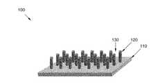
- FIG. 1Ashows a perspective schematic of a nanowire array.
- FIG. 1Bshows a cross sectional schematic of the nanowire array of FIG. 1A .
- FIGS. 2A-2Dare SEM images of an exemplary nanowire array.
- FIG. 3Ashows measured reflectance spectra of nanowire arrays with nanowires of a series of different radii.
- FIG. 3Bshows simulated reflectance spectra of the nanowire arrays of FIG. 3A .
- FIG. 3Cshows dip positions in measured and simulated reflectance spectra of nanowire arrays, as functions of the radii of the nanowires thereon.
- FIG. 4A-4Cshow a major transverse component of the H 1,1 mode at different wavelengths, near a nanowire in an nanowire array.
- FIG. 4Dshows a schematic illustration of possible pathways of white light normally incident on the nanowire array.
- FIG. 5Ashows simulated effective refractive indexes (n eff ) of the H 1,1 modes, as a function of wavelength, of three nanowire arrays with different nanowire radii.
- FIG. 5Bshows simulated absorption spectra of the nanowire arrays of FIG. 5A .
- FIG. 5Ccompares a simulated absorption spectrum of the substrate in a nanowire array, a simulated absorption spectrum of the nanowires (of 45 nm radius) in the nanowire array, and a simulated reflectance spectrum of the entire nanowire array.
- FIG. 6shows a schematic top view of four pixels of the dynamic color display comprising a nanowire array according to an embodiment.
- FIGS. 7A and 7Bshow schematics of two exemplary apparatuses for measuring reflectance spectra of the nanowire array.
- a nanowire arraycomprising a substrate and a plurality of nanowires extending essentially perpendicularly from the substrate; wherein a refractive index of the nanowires is at least two times of a refractive index of a cladding of the nanowires.
- a number density of the nanowirespreferably is at most about 1.8/ ⁇ m 2 .
- a nanowire arraycomprises a substrate and a plurality of nanowires extending essentially perpendicularly from the substrate; wherein the nanowire array is operable as a submicron color filter.
- a “submicron color filter” as used hereinmeans that an optical filter that allows light of certain wavelengths to pass through and optical elements in the filter are less than a micron at least in one dimension.
- a nanowire arraycomprises a substrate and a plurality of nanowires extending essentially perpendicularly from the substrate; wherein the nanowires do not substantially couple.
- substantially couplemeans the nanowires collectively interact with incident light such that spectral properties (e.g., reflectance spectrum) of the nanowire array are distinct from spectral properties of individual nanowire in the nanowire array.
- the nanowires do not substantially couplemeans one nanowire does not affect the properties of a neighboring nanowire. For example, when the pitch of the nanowires is changed and there is no color change of the light absorbed or reflected by the nanowire, then the nanowires do not substantially couple.
- a nanowire arraycomprises a substrate and a plurality of nanowires extending essentially perpendicularly from the substrate; the nanowire array does not appear black to naked eye.
- naked eyeas used herein means human visual perception that is unaided by enhancing equipment.
- the nanowire array does not appear black to naked eyeas used herein means that the reflected visible light from the nanowire is substantially zero, which could happen under certain conditions based on the nanowire length, radius and pitch, as well as the optical properties of the substrate.
- a nanowire as used hereinmeans a structure that has a size constrained to at most 1000 nm in two dimensions and unconstrained in the other dimension.
- An array as used hereinmeans a systematic arrangement of objects such as a grid.
- the term “nanowires extending essentially perpendicularly from the substrate” as used hereinmeans that angles between the nanowires and the substrate are from 85° to 90°.
- Cladding as used hereinmeans a substance surrounding the nanowires, which can be vacuum, air, water, etc.
- a refractive index of the nanowires as used hereinmeans a ratio of the speed of light in vacuum relative to that in the nanowires.
- a number density of the nanowires as used hereinmeans that an average number of nanowires per unit area of the substrate.
- each of the nanowires in the nanowire arrayhas an essentially uniform chemical composition from one end of the nanowire to an opposite end of the nanowire in a longitudinal direction of the nanowire.
- chemical composition of the nanowires as used hereinmeans the simplest whole number ratio of atoms of each element present in the nanowires.
- the term “essentially uniform chemical composition” as used hereinmeans that the ratio of atoms varies at most 3%, preferably at most 1%.
- a longitudinal direction of the nanowire as used hereinmeans a direction pointing from one end of the nanowire farthest from the substrate to one end of the nanowire nearest to the substrate.
- each of the nanowires in the nanowire arrayis single crystalline, multi-crystalline or amorphous. That the nanowire is single crystalline as used herein means that the crystal lattice of the entire nanowire is continuous and unbroken throughout the entire nanowire, with no grain boundaries therein. That the nanowire is multi-crystalline as used herein means that the nanowire comprises grains of crystals separated by grain boundaries. That the nanowire is amorphous as used herein means that the nanowire has a disordered atomic structure.
- the nanowires in the nanowire arrayare composed of a semiconductor or an electrically insulating material.
- a conductorcan be a material with essentially zero band gap. The electrical conductivity of a conductor is generally above 10 3 S/cm.
- a semiconductorcan be a material with a finite band gap up to about 3 eV and general has an electrical conductivity in the range of 10 3 to 10 8 S/cm.
- An electrically insulating materialcan be a material with a band gap greater than about 3 eV and generally has an electrical conductivity below 10 8 S/cm.
- the nanowires in the nanowire arraycomprise one or more materials selected from the group consisting of Si, Ge, GaN, GaAs, SiO 2 , and Si 3 N 4 .
- radii of the nanowires in the nanowire arrayare from 10 to 1000 nm; lengths of the nanowires are from 0.01 to 10 ⁇ m.
- the nanowires and the substrate in the nanowire arrayhave substantially the same chemical composition.
- standard chemical compositionas used herein means that the substrate and the nanowires are identical materials.
- substantially samehere means the chemical composition differs by no more than 3%, preferably by no more than 1%.
- the nanowires and the substrate in the nanowire arrayare single crystalline and the lattices of the nanowires and the lattice of the substrate are continuous at interfaces therebetween. Namely, there is no grain boundary at the interfaces between the nanowires and the substrate.
- the nanowires in the nanowire arrayare arranged in a predetermined pattern such as a rectangular grid, a square grid, concentric circle, hexagonal grid.
- a distance of a nanowire to a nearest neighbor of the nanowire along a direction parallel to the substrateis at least 800 nm, preferably at most 10000 nm.
- a reflectance spectrum of the nanowire arrayhas a dip; the dip position shifts to shorter wavelength with decreasing radii of the nanowires; and the dip position is independent from a distance of a nanowire to a nearest neighbor of the nanowire along a direction parallel to the substrate.
- a reflectance spectrum as used hereinmeans a ratio of the intensity of reflected light at a certain wavelength to the intensity of incident light at the same wavelength, as a function of wavelength.
- a “dip” in a reflectance spectrum as used hereinmeans that a region in the reflectance spectrum wherein the reflectance is smaller than the reflectance in surrounding regions of the reflectance spectrum.
- the “dip position” as used hereinmeans the wavelength in the dip at which the reflectance is a minimum.
- a reflectance spectrum of the nanowire arrayis independent from incident angles of illumination.
- an incident angleas used herein means the angle between a ray of light incident on the substrate and the line perpendicular to the substrate at the point of incidence.
- a method of fabricating the nanowire arraycomprises: (a) coating the substrate with a resist layer; (b) generating a pattern of dots in the resist layer using a lithography technique; (c) developing the pattern in the resist layer; (d) depositing a mask layer; (e) lifting off the resist layer; (f) forming the nanowires by dry etching the substrate; (g) optionally removing the mask player; wherein shapes and sizes of the dots determine the cross-sectional shapes and sizes of the nanowires.
- a resist layer as used hereinmeans a thin layer used to transfer a pattern to the substrate which the resist layer is deposited upon.
- a resist layercan be patterned via lithography to form a (sub)micrometer-scale, temporary mask that protects selected areas of the underlying substrate during subsequent processing steps.
- the resistis generally proprietary mixtures of a polymer or its precursor and other small molecules (e.g. photoacid generators) that have been specially formulated for a given lithography technology. Resists used during photolithography are called photoresists. Resists used during e-beam lithography are called e-beam resists. “Dots” as used herein means discrete regions.
- a lithography techniquecan be photolithography, e-beam lithography, holographic lithography.
- Photolithographyis a process used in microfabrication to selectively remove parts of a thin film or the bulk of a substrate. It uses light to transfer a geometric pattern from a photo mask to a light-sensitive chemical photo resist, or simply “resist,” on the substrate. A series of chemical treatments then engraves the exposure pattern into the material underneath the photo resist. In complex integrated circuits, for example a modern CMOS, a wafer will go through the photolithographic cycle up to 50 times.
- E-beam lithographyis the practice of scanning a beam of electrons in a patterned fashion across a surface covered with a film (called the resist), (“exposing” the resist) and of selectively removing either exposed or non-exposed regions of the resist (“developing”).
- the purpose, as with photolithography,is to create very small structures in the resist that can subsequently be transferred to the substrate material, often by etching. It was developed for manufacturing integrated circuits, and is also used for creating nanotechnology artifacts.
- Holographic lithographyalso known as Interference lithography
- the basic principleis the same as in interferometry or holography.
- An interference pattern between two or more coherent light wavesis set up and recorded in a recording layer (photoresist).
- This interference patternconsists of a periodic series of fringes representing intensity minima and maxima.
- a photoresist pattern corresponding to the periodic intensity patternemerges.
- a mask layeras used herein means a layer that protects an underlying portion of the substrate from being etched.
- “Dry etching” as used hereinmeans an etching technique without using a liquid etchant.
- a method using the nanowire array 1 as a photodetectorcomprises: shining light on the nanowire array; measuring photocurrent on the nanowires; measuring photocurrent on the substrate; comparing the photocurrent on the nanowires to the photocurrent on the substrate.
- a photodetector as used hereinmeans a sensor of light.
- a method using the nanowire array as a static color displaycomprises: determining locations and radii of the nanowires from an image to be displayed; fabricating the nanowires with the determined radii at the determined locations on the substrate; shining white light on the nanowire array.
- a dynamic color displaycomprises the nanowire array, an array of independently addressable white light sources on a side of the substrate opposite the nanowires, wherein each white light source corresponds to and is aligned in the substrate plane with one of the nanowires.
- Independently addressable white light sourcesas used herein mean that each source can be controlled, adjusted, turned on or off, independently from other sources.
- White lightas used herein means a combination of visible light of different wavelengths in equal proportions.
- the white light sources in the dynamic color displayare white LEDs.
- LEDsare also known as light-emitting diodes.
- a first group of the nanowireshave a first radius
- a second group of the nanowireshave a second radius
- a third group of the nanowireshave a third radius
- the first group of the nanowiresonly allow red light to pass
- the second group of the nanowiresonly allow green light to pass
- the third group of the nanowiresonly allow blue light to pass.
- a submicron color filtercomprising the nanowire array, wherein each nanowire is placed on a photodetector, wherein only incident light with wavelengths in a dip of a reflectance spectrum of each nanowire is allowed reach the photodetector below.
- a method using the submicron color filtercomprises shining white light on the nanowire array, detecting transmitted light below the nanowires.
- a ratio of a radius of the nanowires to a pitch of the nanowiresis at most 0.5.
- FIGS. 1A and 1Bshow schematics of a nanowire array 100 , according to an embodiment.
- the nanowire array 100comprises a substrate 110 and a plurality of nanowires 120 extending essentially vertically from the substrate 110 (e.g. angles between the nanowires 120 and the substrate 110 are from 85° to 90°).
- Each nanowire 120preferably has uniform chemical composition along its entire length.
- Each nanowire 120is single crystalline, multi-crystalline or amorphous.
- the nanowires 120preferably are made of a suitable semiconductor or an electrically insulating materials, examples of which include Si, Ge, GaN, GaAs, SiO2, Si 3 N 4 , etc.
- a ratio of the refractive index (i.e., refractive index contrast) of the nanowires 120 and the refractive index of a cladding 130 (i.e., materials surround the nanowires 120 )is preferably at least 2, more preferably at least 3.
- Radii of the nanowires 120preferably are from 10 to 1000 nm, more preferably from 20 to 80 nm, most preferably from 45 to 75 nm.
- Lengths of the nanowires 120are preferably from 0.01 to 10 ⁇ m, more preferably 0.1 to 5 ⁇ m.
- the nanowires 120 and the substrate 110preferably have substantially the same chemical composition.
- Crystal lattices of the nanowires 120 and the substrate 110are preferably continuous at interfaces therebetween.
- the nanowires 120can have the same or different shape and size.
- the nanowires 120can be arranged in any suitable pattern, examples of which include a rectangular grid, a square grid, a hexagonal grid, concentric rings, etc.
- a distance between a nanowire 120 of the nanowire array 100 to a nearest neighbor nanowire of the nanowire array 100 along a direction parallel to the substrateis also known as “pitch” or “pitch distance”.
- a ratio of the radius of the nanowires 120 to the pitchshould not be too high, i.e., preferably at most 0.5, more preferably at most 0.1.
- the nanowires 120substantially couple to each other (i.e., the nanowires 120 collectively interact with incident light such that spectral properties (e.g., reflectance spectrum) of the nanowire array 100 are distinct from spectral properties of individual nanowire 120 in the nanowire array 100 ) and the nanowire array 100 appears black to naked eyes and cannot function as color filters or displays.
- the number density of the nanowires 120(average number of nanowires 120 per unit area on the substrate 110 ) is thus at most about 1.8/ ⁇ m 2 .
- the pitch of the nanowires 120is at least 500 nm.
- FIGS. 2A-2Dshow exemplary scanning electron microscope (SEM) images of the nanowire array 100 .
- SEMscanning electron microscope
- 10,000 nanowires 120 consisting of siliconare arranged in a 100 ⁇ m ⁇ 100 ⁇ m square grid on the substrate 110 consisting of silicon, wherein a distance of one nanowire to a nearest neighbor nanowire of the nanowire array 100 along a direction parallel to the substrate is about 1 ⁇ m.
- the length of the nanowires 120are about 1 ⁇ m.
- the radius of the nanowires 120is about 45 nm.
- FIG. 3Ashows measured reflectance spectra of five nanowire arrays 100 , each of which consists 10,000 nanowires 120 consisting of silicon arranged in a 100 ⁇ m ⁇ 100 ⁇ m square grid on the substrate 110 consisting of silicon, wherein the pitch of these nanowire arrays 100 and the length of the nanowires 120 are about 1 ⁇ m.
- These five nanowire arrays 100are identical except that the nanowires 120 thereof have uniform radii of 45 nm, 50 nm, 55 nm, 60 nm, 65 nm and 70 nm, respectively. Under white light illumination, these nanowire arrays 100 appear to be different colors (e.g., red, green, blue, cyan, etc.) to naked eyes.
- each of these nanowire arrays 100shows one dip, i.e., incident light at wavelengths within the dip is reflected at a lesser proportion compared to incident light at wavelengths outside the dip.
- Positions of the dipdictates the apparent colors of the nanowire arrays 100 . For example, if the position of the dip is between 700 and 635 nm, the nanowire array 100 appears cyan; if the position of the dip is between 560 and 490 nm, the nanowire array 100 appears magenta; if the position of the dip is between 490 and 450 nm, the nanowire 100 appears yellow.
- Position of the dipprogressively shifts to shorter wavelength from about 770 nm in the nanowire array 100 with the largest nanowires 120 (70 nm in radius) to about 550 nm in the nanowire array 100 with the smallest nanowires 120 (45 nm in radius).
- the positions of the dips in these five nanowire arrays 100range across the entire visible spectrum.
- the position of the dipis independent from the pitch of the nanowire array 100 , which indicates that the dips are not due to diffractive or coupling effects. Although diffractive and coupling effects are not required, the nanowire array 100 can function when such effects are present.
- the nanowire array 100preferably has a pitch greater than 800 nm so that diffractive and coupling effects do not dominate.
- FIG. 3Aalso illustrates that magnitudes of the dips increase with the positions of the dips in wavelength, due to strong material dispersion of the substrate material above its bandgap (i.e., the refractive index of the substrate 110 increases at wavelengths above the bandgap of the material thereof while the effective refractive index of a guided mode in the nanowires 120 remains close to the refractive index of air, which leads to higher refractive index contrast between the guided mode and the substrate 110 and thus stronger reflectance in the dip, i.e., smaller magnitude of the dip, at shorter wavelengths).
- more than one dipmay be present in its reflectance spectrum and the nanowire array may appear in a combination of colors.
- the reflectance spectracan be measured with focused or collimated incident illumination.
- An iris 840is used at the image plane of the objective lens 830 to reject any light other than light reflected by the nanowire array 100 .
- An iris 840is used at the image plane of the objective lens 830 to reject any light other than light reflected by the nanowire array 100 .
- incident white light from a light source 815is collimated by a lens 835 and directed to the nanowire array 100 through a beam splitter 825 ; reflected light is collected by a 10 ⁇ objective lens 865 to a spectrometer 855 .
- An iris 845is used at the image plane of the objective lens 865 to reject any light other than light reflected by the nanowire array 100 .
- a silver mirrorcan used to measure absolute intensity of reflected light, which is used to calculate (i.e., normalize) the reflectance spectra. The reflectance spectra are found to be essentially independent from the incident angle, which indicates that the reflectance spectra are dominated by coupling dynamics between normal component of the incident light and the nanowire array 100 .
- FIG. 3Bshows simulated reflectance spectra of the five nanowire arrays 100 in FIG. 3A using the finite difference time domain (FDTD) method.
- the FDTD methodis a method of numerically simulating propagation of light in a structure and can be used to predict detailed characteristics of the propagation.
- the simulated reflectance spectraare quantitatively in good agreement with the measured reflectance spectra of FIG. 3A , with respect to the dip position as a function of nanowire radius.
- simulated spectrahave shallower dips, which could be due to a reflectivity difference between roughened substrate surface in actual nanowire arrays and ideally flat substrate surface presumed in the simulation.
- Lumerical's (Lumerical Solutions, Inc.) FDTD and MODE solverswere used to perform the simulation. Two dimensional models were constructed in MODE solver by simply specifying nanowire radius, pitch and material properties. A periodic boundary condition is then imposed in the substrate plane. These modes were used to study the evolution of the fundamental mode of the nanowires 120 as a function of wavelength. Full three dimensional models were constructed in Lumerical's FDTD solver by specifying complete nanowire geometry along with pitch and material properties. Periodic boundary conditions in the substrate plane and absorbing boundary conditions along the z axis (normal direction of the substrate 110 ) were imposed. A plane wave pulse source of the appropriate bandwidth was launched along the z axis and monitors placed to compute the total absorbed, transmitted and reflected fluxes as a function of wavelength. The nanowires 120 and the substrate 110 were assumed to be silicon in the simulation.
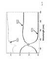
- FIG. 3Cshows the positions of the dips as a function of radii of the nanowires 120 in both of the measured and simulated reflectance spectra, which shows an essentially linear dependence on the nanowire radii.
- the essentially linear dependenceindicates a strong correlation or agreement between the measured and simulated reflectance spectra.
- Wavelength selective reflection of the nanowire array 100 as shown in FIGS. 3A and 3Boriginates from strong wavelength dependence of field distribution of the fundamental guided mode (HE 1,1 mode) of each nanowire 120 .
- the fundamental guided mode as used hereinmeans the guided mode with the lowest frequency.
- the guided mode of a nanowire 120 as used hereinmeans a mode whose field decays monotonically in the transverse direction (directions parallel to the substrate 110 ) everywhere external to the nanowire 120 and which does not lose power to radiation. Symmetry prevents efficient interaction between the nanowire 120 and other guided mode, and the nanowire 120 is too small to support higher order HE 1,m modes (guided modes with higher frequency).
- FIGS. 4A-4Cshow a major transverse component (e.g.
- E y(a field component perpendicular to the direction of propagation of the mode) of the H 1,1 mode at different wavelengths.
- the field distribution of the HE 1,1 mode of each nanowire 120is characterized by a transverse field that is partially contained in the nanowire 120 and partially extends into the cladding 130 , as shown in FIG. 4A .
- Incident light at these wavelengthscan efficiently excite the HE 1,1 mode and be guided by the nanowire 120 to the substrate 110 or be absorbed by the nanowire 120 .
- the large refractive index contrast between the nanowire 120 and the claddingleads to non-negligible longitudinal field component (E z ) (i.e., field component parallel to the direction of propagation of the mode) which has significant overlap with the nanowire 120 ; since the modal absorption is proportional to the spatial density of electromagnetic energy, which includes E z , incident light at these wavelengths can both efficiently couple to (i.e., a significant portion of the incident light propagates inside the nanowire 120 ) and be absorbed by the nanowire 120 .
- E zlongitudinal field component
- the field distribution of the HE 1,1 mode of each nanowire 120is characterized by a transverse field essentially confined in the nanowire 120 due to large refractive index contrast between the nanowire 120 and the cladding, as shown in FIG. 4B .
- Incident light at these wavelengthscannot efficiently excite the HE 1,1 mode and thus cannot be efficiently guided or absorbed by the nanowire 120 ; incident light at these wavelengths is substantially reflected by an interface of the substrate 110 and the cladding 130 .
- the field distribution of the HE 1,1 mode of each nanowire 120is characterized by a transverse field essentially expelled from the nanowire 120 , as shown in FIG. 4C .
- Incident light at these wavelengthscan efficiently excite the HE 1,1 mode but the HE 1,1 mode at these wavelengths cannot be efficiently guided or absorbed by the nanowire 120 ; incident light at these wavelengths is substantially reflected by an interface of the substrate 110 and the cladding.
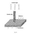
- FIG. 4Dshows schematic illustration of possible pathways of white light normally incident on the nanowire array 100 . Light of wavelengths beyond the dip in the reflectance spectrum is reflected by the substrate 110 ; light of wavelengths in the dip is guided by the nanowire 120 to transmitted through the substrate 110 or absorbed by the nanowire 120 .
- FIG. 5Ashows simulated effective refractive indexes (n eff ) of the H 1,1 modes, as a function of wavelength, of three nanowire arrays 100 with different nanowire radii (45 nm, 55 nm and 70 nm in traces 501 , 502 and 503 , respectively), wherein n eff are obtained by the FDTD method over a 1 ⁇ m by 1 ⁇ am unit cell under periodic boundary conditions, the material of the nanowire arrays 100 is assumed to be silicon, the cladding is assumed to be air, and length of the nanowires 120 is assumed to be 1 ⁇ m.
- a periodic boundary conditionis a set of boundary conditions that are often used to model a large system as an infinite periodic tile of a small unit cell.
- n effincreases sharply and approaches n Si (refractive index of silicon) for wavelengths shorter than the corresponding dip position in FIG. 3A .
- the dipoccurs where n eff asymptotes to n air (refractive index of air).
- n eff as a function of wavelengthalso called a dispersion curve
- FIG. 5Bshows simulated absorption spectra (obtained by the FDTD method) of the nanowire arrays 100 of FIG. 5A (traces 511 , 512 and 513 corresponding to nanowire arrays with nanowires of 45 nm, 55 nm and 70 nm radii, respectively).
- traces 511 , 512 and 513corresponding to nanowire arrays with nanowires of 45 nm, 55 nm and 70 nm radii, respectively.
- 5Ccompares a simulated absorption spectrum 521 of the substrate 110 in the nanowire array 100 with nanowires 120 of 45 nm radius (corresponding to traces 501 and 511 ), a simulated absorption spectrum 523 of the nanowires 120 of 45 nm radius in this nanowire array 100 , and a simulated reflectance spectrum 522 of this nanowire array 100 .
- the dip in the reflectance spectrum 522is slightly redshifted relative to the peak in the absorption spectrum 523 of the nanowires 120 , which indicates that the long wavelength edge of the dip arises more from coupling to the substrate 110 .
- the guided lightis in fact absorbed in the nanowires 120 , and so the shape of the reflectance spectrum 523 and the amount of light absorbed in the nanowires 120 can be controlled by altering the length thereof.
- the light absorbed by the substrate 110can be enhanced or diminished by the nanowires 120 relative to light absorption of a planar substrate, depending on whether the nanowires 120 absorb or merely couple to the substrate 110 .
- the fact that the filtering characteristics of the nanowire array 100 are related to absorption in different parts thereofcan lead to useful applications in optoelectronic devices.
- a method of fabricating the nanowire array 100includes (a) coating the substrate 110 with a resist layer (e.g. e-beam resist, photo resist, etc.); (b) generating a pattern of dots in the resist layer using a lithography technique (e.g. photolithography, e-beam lithography, holographic lithography, etc.); (c) developing the pattern in the resist layer; (d) depositing a mask layer (e.g.
- a resist layere.g. e-beam resist, photo resist, etc.
- a lithography techniquee.g. photolithography, e-beam lithography, holographic lithography, etc.
- the resistcan be poly(methyl methacrylate) (available from MicroChem located in Newton, Mass.).
- the mask layercan be aluminum deposited by a suitable technique such as e-beam evaporation, thermal evaporation, sputtering, etc. The mask layer can be about 40 nm thick.
- the substrate 110can be a single crystalline silicon wafer.
- Dry etchingcan be conducted in an inductively coupled plasma-reactive ion etcher (such as those available from Surface Technology Systems, located at Redwood City, Calif.).
- An exemplary dry etching processincludes alternating etch and deposition steps at room temperature, wherein 60 sccm of SF 6 and 160 sccm of C 4 F 8 gases were used therein, respectively.
- the mask layercan be removed using a suitable etchant (e.g. Type A aluminum etchant available from Transene Company Inc. located in Danvers, Mass.) or solvent (e.g. acid, base, or organic solvent).
- SEM imagescan be taken in an SEM such as Zeiss Ultra55 available from Carl Zeiss NTS located at Peabody, Mass.
- a method using the nanowire array 100 as a photodetectorcomprises shining light on the nanowire array 100 ; measuring photocurrent on the nanowires 120 ; measuring photocurrent on the substrate 110 ; comparing the photocurrent on the nanowires 120 to the photocurrent on the substrate 110 .
- the nanowire array 100can also be used as a submicron color filter.
- each of the nanowires 120 in the nanowire array 100can be placed on a photodetector. Only incident light with wavelengths in the dip of the reflectance spectrum of a nanowire can reach the photodetector below this nanowire.
- a method using the nanowire array 100 as a submicron color filtercomprises shining white light on the nanowire array 100 , detecting transmitted light below the nanowires 120 .
- a method using the nanowire array 100 as a static color displaycomprises: determining locations and radii of nanowires from an image to be displayed; fabricating the nanowires with the determined radii at the determined locations on the substrate; shining white light on the nanowire array.
- the word “static” heremeans that the display can only show one fixed image.
- the nanowire arraycan also be used in a dynamic color display.
- the word “dynamic” heremeans that the display can display different images at different times.
- the dynamic color displaycomprises the nanowire array 100 , an array of independently addressable white light sources on a side of the substrate 110 opposite the nanowires 120 , wherein each white light source corresponds to and is aligned in the substrate plane with one of the nanowires 120 .
- the nanowires 120can have predetermined radii and thus only allow light of desired wavelengths from the light sources to pass. For example, FIG. 6 shows a schematic top view of four pixels of the dynamic color display.
- Nanowires 715 , 725 , 735 and 745respectively correspond to and are aligned with white light sources 710 , 720 , 730 and 740 .
- the white light sourcescan be white LEDs.
- the nanowire 715has a radius of about 45 nm and only allows red light to pass.
- the nanowires 725 and 735have a radius of about 60 nm and only allows green light to pass.
- the nanowire 745has a radius of about 70 nm and only allows blue light to pass.
- the independently addressable white light sourcescan be replaced by a scanning white light beam.
Landscapes
- Engineering & Computer Science (AREA)
- Chemical & Material Sciences (AREA)
- Nanotechnology (AREA)
- Physics & Mathematics (AREA)
- General Physics & Mathematics (AREA)
- Crystallography & Structural Chemistry (AREA)
- Optics & Photonics (AREA)
- Condensed Matter Physics & Semiconductors (AREA)
- Materials Engineering (AREA)
- Manufacturing & Machinery (AREA)
- Life Sciences & Earth Sciences (AREA)
- Biophysics (AREA)
- Composite Materials (AREA)
- Spectroscopy & Molecular Physics (AREA)
- General Engineering & Computer Science (AREA)
- Theoretical Computer Science (AREA)
- Light Receiving Elements (AREA)
- Optical Filters (AREA)
- Polarising Elements (AREA)
- Thin Film Transistor (AREA)
- Diffracting Gratings Or Hologram Optical Elements (AREA)
Abstract
Description
Claims (35)
Priority Applications (19)
| Application Number | Priority Date | Filing Date | Title |
|---|---|---|---|
| US12/910,664US9000353B2 (en) | 2010-06-22 | 2010-10-22 | Light absorption and filtering properties of vertically oriented semiconductor nano wires |
| US12/945,492US9515218B2 (en) | 2008-09-04 | 2010-11-12 | Vertical pillar structured photovoltaic devices with mirrors and optical claddings |
| KR1020137011820AKR101377795B1 (en) | 2010-10-22 | 2011-10-21 | Light absorption and filtering properties of vertically oriented semiconductor nano wires |
| PCT/US2011/057325WO2012094047A2 (en) | 2010-10-22 | 2011-10-21 | Light absorption and filtering properties of vertically oriented semiconductor nano wires |
| CN201180051048.XACN103168360B (en) | 2010-10-22 | 2011-10-21 | The light of the semiconductor nanowires of vertical orientation absorbs and filtering feature |
| TW100138526ATW201231381A (en) | 2010-10-22 | 2011-10-24 | Light absorption and filtering properties of vertically oriented semiconductor nano wires |
| US13/925,429US9304035B2 (en) | 2008-09-04 | 2013-06-24 | Vertical waveguides with various functionality on integrated circuits |
| US14/503,598US9410843B2 (en) | 2008-09-04 | 2014-10-01 | Nanowire arrays comprising fluorescent nanowires and substrate |
| US14/516,162US20160111562A1 (en) | 2008-09-04 | 2014-10-16 | Multispectral and polarization-selective detector |
| US14/516,402US20160111460A1 (en) | 2008-09-04 | 2014-10-16 | Back-lit photodetector |
| US14/632,739US9601529B2 (en) | 2008-09-04 | 2015-02-26 | Light absorption and filtering properties of vertically oriented semiconductor nano wires |
| US14/704,143US20150303333A1 (en) | 2008-09-04 | 2015-05-05 | Passivated upstanding nanostructures and methods of making the same |
| US14/705,380US9337220B2 (en) | 2008-09-04 | 2015-05-06 | Solar blind ultra violet (UV) detector and fabrication methods of the same |
| US15/057,153US20160178840A1 (en) | 2008-09-04 | 2016-03-01 | Optical waveguides in image sensors |
| US15/082,514US20160211394A1 (en) | 2008-11-13 | 2016-03-28 | Nano wire array based solar energy harvesting device |
| US15/090,155US20160216523A1 (en) | 2008-09-04 | 2016-04-04 | Vertical waveguides with various functionality on integrated circuits |
| US15/093,928US20160225811A1 (en) | 2008-09-04 | 2016-04-08 | Nanowire structured color filter arrays and fabrication method of the same |
| US15/149,252US20160254301A1 (en) | 2008-09-04 | 2016-05-09 | Solar blind ultra violet (uv) detector and fabrication methods of the same |
| US15/225,264US20160344964A1 (en) | 2008-09-04 | 2016-08-01 | Methods for fabricating and using nanowires |
Applications Claiming Priority (2)
| Application Number | Priority Date | Filing Date | Title |
|---|---|---|---|
| US35742910P | 2010-06-22 | 2010-06-22 | |
| US12/910,664US9000353B2 (en) | 2010-06-22 | 2010-10-22 | Light absorption and filtering properties of vertically oriented semiconductor nano wires |
Related Child Applications (1)
| Application Number | Title | Priority Date | Filing Date |
|---|---|---|---|
| US14/632,739ContinuationUS9601529B2 (en) | 2008-09-04 | 2015-02-26 | Light absorption and filtering properties of vertically oriented semiconductor nano wires |
Publications (2)
| Publication Number | Publication Date |
|---|---|
| US20110309237A1 US20110309237A1 (en) | 2011-12-22 |
| US9000353B2true US9000353B2 (en) | 2015-04-07 |
Family
ID=46489528
Family Applications (4)
| Application Number | Title | Priority Date | Filing Date |
|---|---|---|---|
| US12/910,664Expired - Fee RelatedUS9000353B2 (en) | 2008-09-04 | 2010-10-22 | Light absorption and filtering properties of vertically oriented semiconductor nano wires |
| US14/632,739Expired - Fee RelatedUS9601529B2 (en) | 2008-09-04 | 2015-02-26 | Light absorption and filtering properties of vertically oriented semiconductor nano wires |
| US14/705,380Expired - Fee RelatedUS9337220B2 (en) | 2008-09-04 | 2015-05-06 | Solar blind ultra violet (UV) detector and fabrication methods of the same |
| US15/149,252AbandonedUS20160254301A1 (en) | 2008-09-04 | 2016-05-09 | Solar blind ultra violet (uv) detector and fabrication methods of the same |
Family Applications After (3)
| Application Number | Title | Priority Date | Filing Date |
|---|---|---|---|
| US14/632,739Expired - Fee RelatedUS9601529B2 (en) | 2008-09-04 | 2015-02-26 | Light absorption and filtering properties of vertically oriented semiconductor nano wires |
| US14/705,380Expired - Fee RelatedUS9337220B2 (en) | 2008-09-04 | 2015-05-06 | Solar blind ultra violet (UV) detector and fabrication methods of the same |
| US15/149,252AbandonedUS20160254301A1 (en) | 2008-09-04 | 2016-05-09 | Solar blind ultra violet (uv) detector and fabrication methods of the same |
Country Status (5)
| Country | Link |
|---|---|
| US (4) | US9000353B2 (en) |
| KR (1) | KR101377795B1 (en) |
| CN (1) | CN103168360B (en) |
| TW (1) | TW201231381A (en) |
| WO (1) | WO2012094047A2 (en) |
Cited By (177)
| Publication number | Priority date | Publication date | Assignee | Title |
|---|---|---|---|---|
| US9154966B2 (en) | 2013-11-06 | 2015-10-06 | At&T Intellectual Property I, Lp | Surface-wave communications and methods thereof |
| US9209902B2 (en) | 2013-12-10 | 2015-12-08 | At&T Intellectual Property I, L.P. | Quasi-optical coupler |
| US9299866B2 (en) | 2010-12-30 | 2016-03-29 | Zena Technologies, Inc. | Nanowire array based solar energy harvesting device |
| US9304035B2 (en) | 2008-09-04 | 2016-04-05 | Zena Technologies, Inc. | Vertical waveguides with various functionality on integrated circuits |
| US9312919B1 (en) | 2014-10-21 | 2016-04-12 | At&T Intellectual Property I, Lp | Transmission device with impairment compensation and methods for use therewith |
| US9337220B2 (en) | 2008-09-04 | 2016-05-10 | Zena Technologies, Inc. | Solar blind ultra violet (UV) detector and fabrication methods of the same |
| US9343490B2 (en) | 2013-08-09 | 2016-05-17 | Zena Technologies, Inc. | Nanowire structured color filter arrays and fabrication method of the same |
| US9406709B2 (en) | 2010-06-22 | 2016-08-02 | President And Fellows Of Harvard College | Methods for fabricating and using nanowires |
| US9412614B2 (en) | 2014-05-29 | 2016-08-09 | Taiwan Semiconductor Manufacturing Company, Ltd. | Nano wire structure and method for fabricating the same |
| US9410843B2 (en) | 2008-09-04 | 2016-08-09 | Zena Technologies, Inc. | Nanowire arrays comprising fluorescent nanowires and substrate |
| US9461706B1 (en) | 2015-07-31 | 2016-10-04 | At&T Intellectual Property I, Lp | Method and apparatus for exchanging communication signals |
| US9478685B2 (en) | 2014-06-23 | 2016-10-25 | Zena Technologies, Inc. | Vertical pillar structured infrared detector and fabrication method for the same |
| US9490283B2 (en) | 2009-11-19 | 2016-11-08 | Zena Technologies, Inc. | Active pixel sensor with nanowire structured photodetectors |
| US9490869B1 (en) | 2015-05-14 | 2016-11-08 | At&T Intellectual Property I, L.P. | Transmission medium having multiple cores and methods for use therewith |
| US9503189B2 (en) | 2014-10-10 | 2016-11-22 | At&T Intellectual Property I, L.P. | Method and apparatus for arranging communication sessions in a communication system |
| US9509415B1 (en) | 2015-06-25 | 2016-11-29 | At&T Intellectual Property I, L.P. | Methods and apparatus for inducing a fundamental wave mode on a transmission medium |
| US9515218B2 (en) | 2008-09-04 | 2016-12-06 | Zena Technologies, Inc. | Vertical pillar structured photovoltaic devices with mirrors and optical claddings |
| US9520945B2 (en) | 2014-10-21 | 2016-12-13 | At&T Intellectual Property I, L.P. | Apparatus for providing communication services and methods thereof |
| US9525524B2 (en) | 2013-05-31 | 2016-12-20 | At&T Intellectual Property I, L.P. | Remote distributed antenna system |
| US9525210B2 (en) | 2014-10-21 | 2016-12-20 | At&T Intellectual Property I, L.P. | Guided-wave transmission device with non-fundamental mode propagation and methods for use therewith |
| US9531427B2 (en) | 2014-11-20 | 2016-12-27 | At&T Intellectual Property I, L.P. | Transmission device with mode division multiplexing and methods for use therewith |
| US9543458B2 (en) | 2010-12-14 | 2017-01-10 | Zena Technologies, Inc. | Full color single pixel including doublet or quadruplet Si nanowires for image sensors |
| US9564947B2 (en) | 2014-10-21 | 2017-02-07 | At&T Intellectual Property I, L.P. | Guided-wave transmission device with diversity and methods for use therewith |
| US9577307B2 (en) | 2014-10-21 | 2017-02-21 | At&T Intellectual Property I, L.P. | Guided-wave transmission device and methods for use therewith |
| US9608692B2 (en) | 2015-06-11 | 2017-03-28 | At&T Intellectual Property I, L.P. | Repeater and methods for use therewith |
| US9608740B2 (en) | 2015-07-15 | 2017-03-28 | At&T Intellectual Property I, L.P. | Method and apparatus for launching a wave mode that mitigates interference |
| US9615269B2 (en) | 2014-10-02 | 2017-04-04 | At&T Intellectual Property I, L.P. | Method and apparatus that provides fault tolerance in a communication network |
| US9628854B2 (en) | 2014-09-29 | 2017-04-18 | At&T Intellectual Property I, L.P. | Method and apparatus for distributing content in a communication network |
| US9628116B2 (en) | 2015-07-14 | 2017-04-18 | At&T Intellectual Property I, L.P. | Apparatus and methods for transmitting wireless signals |
| US9640850B2 (en) | 2015-06-25 | 2017-05-02 | At&T Intellectual Property I, L.P. | Methods and apparatus for inducing a non-fundamental wave mode on a transmission medium |
| US9654173B2 (en) | 2014-11-20 | 2017-05-16 | At&T Intellectual Property I, L.P. | Apparatus for powering a communication device and methods thereof |
| US9653770B2 (en) | 2014-10-21 | 2017-05-16 | At&T Intellectual Property I, L.P. | Guided wave coupler, coupling module and methods for use therewith |
| US9667317B2 (en) | 2015-06-15 | 2017-05-30 | At&T Intellectual Property I, L.P. | Method and apparatus for providing security using network traffic adjustments |
| US9680670B2 (en) | 2014-11-20 | 2017-06-13 | At&T Intellectual Property I, L.P. | Transmission device with channel equalization and control and methods for use therewith |
| US20170170220A1 (en)* | 2015-12-14 | 2017-06-15 | Samsung Electronics Co., Ltd. | Image sensor having hybrid color filter |
| US9685992B2 (en) | 2014-10-03 | 2017-06-20 | At&T Intellectual Property I, L.P. | Circuit panel network and methods thereof |
| US9692101B2 (en) | 2014-08-26 | 2017-06-27 | At&T Intellectual Property I, L.P. | Guided wave couplers for coupling electromagnetic waves between a waveguide surface and a surface of a wire |
| US9699785B2 (en) | 2012-12-05 | 2017-07-04 | At&T Intellectual Property I, L.P. | Backhaul link for distributed antenna system |
| US9705571B2 (en) | 2015-09-16 | 2017-07-11 | At&T Intellectual Property I, L.P. | Method and apparatus for use with a radio distributed antenna system |
| US9705561B2 (en) | 2015-04-24 | 2017-07-11 | At&T Intellectual Property I, L.P. | Directional coupling device and methods for use therewith |
| US9722318B2 (en) | 2015-07-14 | 2017-08-01 | At&T Intellectual Property I, L.P. | Method and apparatus for coupling an antenna to a device |
| US9729197B2 (en) | 2015-10-01 | 2017-08-08 | At&T Intellectual Property I, L.P. | Method and apparatus for communicating network management traffic over a network |
| US9735833B2 (en) | 2015-07-31 | 2017-08-15 | At&T Intellectual Property I, L.P. | Method and apparatus for communications management in a neighborhood network |
| US9742462B2 (en) | 2014-12-04 | 2017-08-22 | At&T Intellectual Property I, L.P. | Transmission medium and communication interfaces and methods for use therewith |
| US9749013B2 (en) | 2015-03-17 | 2017-08-29 | At&T Intellectual Property I, L.P. | Method and apparatus for reducing attenuation of electromagnetic waves guided by a transmission medium |
| US9748626B2 (en) | 2015-05-14 | 2017-08-29 | At&T Intellectual Property I, L.P. | Plurality of cables having different cross-sectional shapes which are bundled together to form a transmission medium |
| US9749053B2 (en) | 2015-07-23 | 2017-08-29 | At&T Intellectual Property I, L.P. | Node device, repeater and methods for use therewith |
| US9755697B2 (en) | 2014-09-15 | 2017-09-05 | At&T Intellectual Property I, L.P. | Method and apparatus for sensing a condition in a transmission medium of electromagnetic waves |
| US9762289B2 (en) | 2014-10-14 | 2017-09-12 | At&T Intellectual Property I, L.P. | Method and apparatus for transmitting or receiving signals in a transportation system |
| US9769128B2 (en) | 2015-09-28 | 2017-09-19 | At&T Intellectual Property I, L.P. | Method and apparatus for encryption of communications over a network |
| US9769020B2 (en) | 2014-10-21 | 2017-09-19 | At&T Intellectual Property I, L.P. | Method and apparatus for responding to events affecting communications in a communication network |
| US9780834B2 (en) | 2014-10-21 | 2017-10-03 | At&T Intellectual Property I, L.P. | Method and apparatus for transmitting electromagnetic waves |
| US9793951B2 (en) | 2015-07-15 | 2017-10-17 | At&T Intellectual Property I, L.P. | Method and apparatus for launching a wave mode that mitigates interference |
| US9793954B2 (en) | 2015-04-28 | 2017-10-17 | At&T Intellectual Property I, L.P. | Magnetic coupling device and methods for use therewith |
| US9793955B2 (en) | 2015-04-24 | 2017-10-17 | At&T Intellectual Property I, Lp | Passive electrical coupling device and methods for use therewith |
| US9800327B2 (en) | 2014-11-20 | 2017-10-24 | At&T Intellectual Property I, L.P. | Apparatus for controlling operations of a communication device and methods thereof |
| US9820146B2 (en) | 2015-06-12 | 2017-11-14 | At&T Intellectual Property I, L.P. | Method and apparatus for authentication and identity management of communicating devices |
| US9838896B1 (en) | 2016-12-09 | 2017-12-05 | At&T Intellectual Property I, L.P. | Method and apparatus for assessing network coverage |
| US9836957B2 (en) | 2015-07-14 | 2017-12-05 | At&T Intellectual Property I, L.P. | Method and apparatus for communicating with premises equipment |
| US9847566B2 (en) | 2015-07-14 | 2017-12-19 | At&T Intellectual Property I, L.P. | Method and apparatus for adjusting a field of a signal to mitigate interference |
| US9847850B2 (en) | 2014-10-14 | 2017-12-19 | At&T Intellectual Property I, L.P. | Method and apparatus for adjusting a mode of communication in a communication network |
| US9853342B2 (en) | 2015-07-14 | 2017-12-26 | At&T Intellectual Property I, L.P. | Dielectric transmission medium connector and methods for use therewith |
| US9860075B1 (en) | 2016-08-26 | 2018-01-02 | At&T Intellectual Property I, L.P. | Method and communication node for broadband distribution |
| US9865911B2 (en) | 2015-06-25 | 2018-01-09 | At&T Intellectual Property I, L.P. | Waveguide system for slot radiating first electromagnetic waves that are combined into a non-fundamental wave mode second electromagnetic wave on a transmission medium |
| US9866309B2 (en) | 2015-06-03 | 2018-01-09 | At&T Intellectual Property I, Lp | Host node device and methods for use therewith |
| US9871283B2 (en) | 2015-07-23 | 2018-01-16 | At&T Intellectual Property I, Lp | Transmission medium having a dielectric core comprised of plural members connected by a ball and socket configuration |
| US9871282B2 (en) | 2015-05-14 | 2018-01-16 | At&T Intellectual Property I, L.P. | At least one transmission medium having a dielectric surface that is covered at least in part by a second dielectric |
| US9876264B2 (en) | 2015-10-02 | 2018-01-23 | At&T Intellectual Property I, Lp | Communication system, guided wave switch and methods for use therewith |
| US9876571B2 (en) | 2015-02-20 | 2018-01-23 | At&T Intellectual Property I, Lp | Guided-wave transmission device with non-fundamental mode propagation and methods for use therewith |
| US9876605B1 (en) | 2016-10-21 | 2018-01-23 | At&T Intellectual Property I, L.P. | Launcher and coupling system to support desired guided wave mode |
| US9882277B2 (en) | 2015-10-02 | 2018-01-30 | At&T Intellectual Property I, Lp | Communication device and antenna assembly with actuated gimbal mount |
| US9882257B2 (en) | 2015-07-14 | 2018-01-30 | At&T Intellectual Property I, L.P. | Method and apparatus for launching a wave mode that mitigates interference |
| US9893795B1 (en) | 2016-12-07 | 2018-02-13 | At&T Intellectual Property I, Lp | Method and repeater for broadband distribution |
| US9906269B2 (en) | 2014-09-17 | 2018-02-27 | At&T Intellectual Property I, L.P. | Monitoring and mitigating conditions in a communication network |
| US9904535B2 (en) | 2015-09-14 | 2018-02-27 | At&T Intellectual Property I, L.P. | Method and apparatus for distributing software |
| US9912382B2 (en) | 2015-06-03 | 2018-03-06 | At&T Intellectual Property I, Lp | Network termination and methods for use therewith |
| US9913139B2 (en) | 2015-06-09 | 2018-03-06 | At&T Intellectual Property I, L.P. | Signal fingerprinting for authentication of communicating devices |
| US9911020B1 (en) | 2016-12-08 | 2018-03-06 | At&T Intellectual Property I, L.P. | Method and apparatus for tracking via a radio frequency identification device |
| US9912419B1 (en) | 2016-08-24 | 2018-03-06 | At&T Intellectual Property I, L.P. | Method and apparatus for managing a fault in a distributed antenna system |
| US9912027B2 (en) | 2015-07-23 | 2018-03-06 | At&T Intellectual Property I, L.P. | Method and apparatus for exchanging communication signals |
| US9917341B2 (en) | 2015-05-27 | 2018-03-13 | At&T Intellectual Property I, L.P. | Apparatus and method for launching electromagnetic waves and for modifying radial dimensions of the propagating electromagnetic waves |
| US9927517B1 (en) | 2016-12-06 | 2018-03-27 | At&T Intellectual Property I, L.P. | Apparatus and methods for sensing rainfall |
| US9948354B2 (en) | 2015-04-28 | 2018-04-17 | At&T Intellectual Property I, L.P. | Magnetic coupling device with reflective plate and methods for use therewith |
| US9948333B2 (en) | 2015-07-23 | 2018-04-17 | At&T Intellectual Property I, L.P. | Method and apparatus for wireless communications to mitigate interference |
| US9954287B2 (en) | 2014-11-20 | 2018-04-24 | At&T Intellectual Property I, L.P. | Apparatus for converting wireless signals and electromagnetic waves and methods thereof |
| US9967173B2 (en) | 2015-07-31 | 2018-05-08 | At&T Intellectual Property I, L.P. | Method and apparatus for authentication and identity management of communicating devices |
| US9973940B1 (en) | 2017-02-27 | 2018-05-15 | At&T Intellectual Property I, L.P. | Apparatus and methods for dynamic impedance matching of a guided wave launcher |
| US9991580B2 (en) | 2016-10-21 | 2018-06-05 | At&T Intellectual Property I, L.P. | Launcher and coupling system for guided wave mode cancellation |
| US9998870B1 (en) | 2016-12-08 | 2018-06-12 | At&T Intellectual Property I, L.P. | Method and apparatus for proximity sensing |
| US9997819B2 (en) | 2015-06-09 | 2018-06-12 | At&T Intellectual Property I, L.P. | Transmission medium and method for facilitating propagation of electromagnetic waves via a core |
| US9999038B2 (en) | 2013-05-31 | 2018-06-12 | At&T Intellectual Property I, L.P. | Remote distributed antenna system |
| US10009063B2 (en) | 2015-09-16 | 2018-06-26 | At&T Intellectual Property I, L.P. | Method and apparatus for use with a radio distributed antenna system having an out-of-band reference signal |
| US10009901B2 (en) | 2015-09-16 | 2018-06-26 | At&T Intellectual Property I, L.P. | Method, apparatus, and computer-readable storage medium for managing utilization of wireless resources between base stations |
| US10009067B2 (en) | 2014-12-04 | 2018-06-26 | At&T Intellectual Property I, L.P. | Method and apparatus for configuring a communication interface |
| US10009065B2 (en) | 2012-12-05 | 2018-06-26 | At&T Intellectual Property I, L.P. | Backhaul link for distributed antenna system |
| US10020587B2 (en) | 2015-07-31 | 2018-07-10 | At&T Intellectual Property I, L.P. | Radial antenna and methods for use therewith |
| US10020844B2 (en) | 2016-12-06 | 2018-07-10 | T&T Intellectual Property I, L.P. | Method and apparatus for broadcast communication via guided waves |
| US10027397B2 (en) | 2016-12-07 | 2018-07-17 | At&T Intellectual Property I, L.P. | Distributed antenna system and methods for use therewith |
| US10033107B2 (en) | 2015-07-14 | 2018-07-24 | At&T Intellectual Property I, L.P. | Method and apparatus for coupling an antenna to a device |
| US10033108B2 (en) | 2015-07-14 | 2018-07-24 | At&T Intellectual Property I, L.P. | Apparatus and methods for generating an electromagnetic wave having a wave mode that mitigates interference |
| US10044409B2 (en) | 2015-07-14 | 2018-08-07 | At&T Intellectual Property I, L.P. | Transmission medium and methods for use therewith |
| US10051483B2 (en) | 2015-10-16 | 2018-08-14 | At&T Intellectual Property I, L.P. | Method and apparatus for directing wireless signals |
| US10051629B2 (en) | 2015-09-16 | 2018-08-14 | At&T Intellectual Property I, L.P. | Method and apparatus for use with a radio distributed antenna system having an in-band reference signal |
| US10069535B2 (en) | 2016-12-08 | 2018-09-04 | At&T Intellectual Property I, L.P. | Apparatus and methods for launching electromagnetic waves having a certain electric field structure |
| US10074890B2 (en) | 2015-10-02 | 2018-09-11 | At&T Intellectual Property I, L.P. | Communication device and antenna with integrated light assembly |
| US10079661B2 (en) | 2015-09-16 | 2018-09-18 | At&T Intellectual Property I, L.P. | Method and apparatus for use with a radio distributed antenna system having a clock reference |
| US10090594B2 (en) | 2016-11-23 | 2018-10-02 | At&T Intellectual Property I, L.P. | Antenna system having structural configurations for assembly |
| US10090606B2 (en) | 2015-07-15 | 2018-10-02 | At&T Intellectual Property I, L.P. | Antenna system with dielectric array and methods for use therewith |
| US10103422B2 (en) | 2016-12-08 | 2018-10-16 | At&T Intellectual Property I, L.P. | Method and apparatus for mounting network devices |
| US10103801B2 (en) | 2015-06-03 | 2018-10-16 | At&T Intellectual Property I, L.P. | Host node device and methods for use therewith |
| US10135145B2 (en) | 2016-12-06 | 2018-11-20 | At&T Intellectual Property I, L.P. | Apparatus and methods for generating an electromagnetic wave along a transmission medium |
| US10135147B2 (en) | 2016-10-18 | 2018-11-20 | At&T Intellectual Property I, L.P. | Apparatus and methods for launching guided waves via an antenna |
| US10136434B2 (en) | 2015-09-16 | 2018-11-20 | At&T Intellectual Property I, L.P. | Method and apparatus for use with a radio distributed antenna system having an ultra-wideband control channel |
| US10135146B2 (en) | 2016-10-18 | 2018-11-20 | At&T Intellectual Property I, L.P. | Apparatus and methods for launching guided waves via circuits |
| US10139820B2 (en) | 2016-12-07 | 2018-11-27 | At&T Intellectual Property I, L.P. | Method and apparatus for deploying equipment of a communication system |
| US10142086B2 (en) | 2015-06-11 | 2018-11-27 | At&T Intellectual Property I, L.P. | Repeater and methods for use therewith |
| US10144036B2 (en) | 2015-01-30 | 2018-12-04 | At&T Intellectual Property I, L.P. | Method and apparatus for mitigating interference affecting a propagation of electromagnetic waves guided by a transmission medium |
| US10148016B2 (en) | 2015-07-14 | 2018-12-04 | At&T Intellectual Property I, L.P. | Apparatus and methods for communicating utilizing an antenna array |
| US10154493B2 (en) | 2015-06-03 | 2018-12-11 | At&T Intellectual Property I, L.P. | Network termination and methods for use therewith |
| US10168695B2 (en) | 2016-12-07 | 2019-01-01 | At&T Intellectual Property I, L.P. | Method and apparatus for controlling an unmanned aircraft |
| US10170840B2 (en) | 2015-07-14 | 2019-01-01 | At&T Intellectual Property I, L.P. | Apparatus and methods for sending or receiving electromagnetic signals |
| US10178445B2 (en) | 2016-11-23 | 2019-01-08 | At&T Intellectual Property I, L.P. | Methods, devices, and systems for load balancing between a plurality of waveguides |
| US10205655B2 (en) | 2015-07-14 | 2019-02-12 | At&T Intellectual Property I, L.P. | Apparatus and methods for communicating utilizing an antenna array and multiple communication paths |
| US10224634B2 (en) | 2016-11-03 | 2019-03-05 | At&T Intellectual Property I, L.P. | Methods and apparatus for adjusting an operational characteristic of an antenna |
| US10225025B2 (en) | 2016-11-03 | 2019-03-05 | At&T Intellectual Property I, L.P. | Method and apparatus for detecting a fault in a communication system |
| US10243784B2 (en) | 2014-11-20 | 2019-03-26 | At&T Intellectual Property I, L.P. | System for generating topology information and methods thereof |
| US10243270B2 (en) | 2016-12-07 | 2019-03-26 | At&T Intellectual Property I, L.P. | Beam adaptive multi-feed dielectric antenna system and methods for use therewith |
| US10264586B2 (en) | 2016-12-09 | 2019-04-16 | At&T Mobility Ii Llc | Cloud-based packet controller and methods for use therewith |
| US10291311B2 (en) | 2016-09-09 | 2019-05-14 | At&T Intellectual Property I, L.P. | Method and apparatus for mitigating a fault in a distributed antenna system |
| US10291334B2 (en) | 2016-11-03 | 2019-05-14 | At&T Intellectual Property I, L.P. | System for detecting a fault in a communication system |
| US10298293B2 (en) | 2017-03-13 | 2019-05-21 | At&T Intellectual Property I, L.P. | Apparatus of communication utilizing wireless network devices |
| US10305190B2 (en) | 2016-12-01 | 2019-05-28 | At&T Intellectual Property I, L.P. | Reflecting dielectric antenna system and methods for use therewith |
| US10312567B2 (en) | 2016-10-26 | 2019-06-04 | At&T Intellectual Property I, L.P. | Launcher with planar strip antenna and methods for use therewith |
| US10320586B2 (en) | 2015-07-14 | 2019-06-11 | At&T Intellectual Property I, L.P. | Apparatus and methods for generating non-interfering electromagnetic waves on an insulated transmission medium |
| US10326494B2 (en) | 2016-12-06 | 2019-06-18 | At&T Intellectual Property I, L.P. | Apparatus for measurement de-embedding and methods for use therewith |
| US10326689B2 (en) | 2016-12-08 | 2019-06-18 | At&T Intellectual Property I, L.P. | Method and system for providing alternative communication paths |
| US10340601B2 (en) | 2016-11-23 | 2019-07-02 | At&T Intellectual Property I, L.P. | Multi-antenna system and methods for use therewith |
| US10340983B2 (en) | 2016-12-09 | 2019-07-02 | At&T Intellectual Property I, L.P. | Method and apparatus for surveying remote sites via guided wave communications |
| US10340573B2 (en) | 2016-10-26 | 2019-07-02 | At&T Intellectual Property I, L.P. | Launcher with cylindrical coupling device and methods for use therewith |
| US10340600B2 (en) | 2016-10-18 | 2019-07-02 | At&T Intellectual Property I, L.P. | Apparatus and methods for launching guided waves via plural waveguide systems |
| US10340603B2 (en) | 2016-11-23 | 2019-07-02 | At&T Intellectual Property I, L.P. | Antenna system having shielded structural configurations for assembly |
| US10341142B2 (en) | 2015-07-14 | 2019-07-02 | At&T Intellectual Property I, L.P. | Apparatus and methods for generating non-interfering electromagnetic waves on an uninsulated conductor |
| US10348391B2 (en) | 2015-06-03 | 2019-07-09 | At&T Intellectual Property I, L.P. | Client node device with frequency conversion and methods for use therewith |
| US10355367B2 (en) | 2015-10-16 | 2019-07-16 | At&T Intellectual Property I, L.P. | Antenna structure for exchanging wireless signals |
| US10361489B2 (en) | 2016-12-01 | 2019-07-23 | At&T Intellectual Property I, L.P. | Dielectric dish antenna system and methods for use therewith |
| US10359749B2 (en) | 2016-12-07 | 2019-07-23 | At&T Intellectual Property I, L.P. | Method and apparatus for utilities management via guided wave communication |
| US10374316B2 (en) | 2016-10-21 | 2019-08-06 | At&T Intellectual Property I, L.P. | System and dielectric antenna with non-uniform dielectric |
| US10382976B2 (en) | 2016-12-06 | 2019-08-13 | At&T Intellectual Property I, L.P. | Method and apparatus for managing wireless communications based on communication paths and network device positions |
| US10389037B2 (en) | 2016-12-08 | 2019-08-20 | At&T Intellectual Property I, L.P. | Apparatus and methods for selecting sections of an antenna array and use therewith |
| US10389029B2 (en) | 2016-12-07 | 2019-08-20 | At&T Intellectual Property I, L.P. | Multi-feed dielectric antenna system with core selection and methods for use therewith |
| US10396887B2 (en) | 2015-06-03 | 2019-08-27 | At&T Intellectual Property I, L.P. | Client node device and methods for use therewith |
| US10411356B2 (en) | 2016-12-08 | 2019-09-10 | At&T Intellectual Property I, L.P. | Apparatus and methods for selectively targeting communication devices with an antenna array |
| US10439675B2 (en) | 2016-12-06 | 2019-10-08 | At&T Intellectual Property I, L.P. | Method and apparatus for repeating guided wave communication signals |
| US10446936B2 (en) | 2016-12-07 | 2019-10-15 | At&T Intellectual Property I, L.P. | Multi-feed dielectric antenna system and methods for use therewith |
| US10498044B2 (en) | 2016-11-03 | 2019-12-03 | At&T Intellectual Property I, L.P. | Apparatus for configuring a surface of an antenna |
| US10530505B2 (en) | 2016-12-08 | 2020-01-07 | At&T Intellectual Property I, L.P. | Apparatus and methods for launching electromagnetic waves along a transmission medium |
| US10535928B2 (en) | 2016-11-23 | 2020-01-14 | At&T Intellectual Property I, L.P. | Antenna system and methods for use therewith |
| US10547348B2 (en) | 2016-12-07 | 2020-01-28 | At&T Intellectual Property I, L.P. | Method and apparatus for switching transmission mediums in a communication system |
| US10601494B2 (en) | 2016-12-08 | 2020-03-24 | At&T Intellectual Property I, L.P. | Dual-band communication device and method for use therewith |
| US10637149B2 (en) | 2016-12-06 | 2020-04-28 | At&T Intellectual Property I, L.P. | Injection molded dielectric antenna and methods for use therewith |
| US10650940B2 (en) | 2015-05-15 | 2020-05-12 | At&T Intellectual Property I, L.P. | Transmission medium having a conductive material and methods for use therewith |
| US10665942B2 (en) | 2015-10-16 | 2020-05-26 | At&T Intellectual Property I, L.P. | Method and apparatus for adjusting wireless communications |
| US10679767B2 (en) | 2015-05-15 | 2020-06-09 | At&T Intellectual Property I, L.P. | Transmission medium having a conductive material and methods for use therewith |
| US10694379B2 (en) | 2016-12-06 | 2020-06-23 | At&T Intellectual Property I, L.P. | Waveguide system with device-based authentication and methods for use therewith |
| US10727599B2 (en) | 2016-12-06 | 2020-07-28 | At&T Intellectual Property I, L.P. | Launcher with slot antenna and methods for use therewith |
| US10739188B2 (en) | 2016-03-10 | 2020-08-11 | Samsung Electronics Co., Ltd. | Color filter array having color filters, and image sensor and display device including the color filter array |
| US10755542B2 (en) | 2016-12-06 | 2020-08-25 | At&T Intellectual Property I, L.P. | Method and apparatus for surveillance via guided wave communication |
| US10777873B2 (en) | 2016-12-08 | 2020-09-15 | At&T Intellectual Property I, L.P. | Method and apparatus for mounting network devices |
| US10784670B2 (en) | 2015-07-23 | 2020-09-22 | At&T Intellectual Property I, L.P. | Antenna support for aligning an antenna |
| US10811767B2 (en) | 2016-10-21 | 2020-10-20 | At&T Intellectual Property I, L.P. | System and dielectric antenna with convex dielectric radome |
| US10819035B2 (en) | 2016-12-06 | 2020-10-27 | At&T Intellectual Property I, L.P. | Launcher with helical antenna and methods for use therewith |
| US10916969B2 (en) | 2016-12-08 | 2021-02-09 | At&T Intellectual Property I, L.P. | Method and apparatus for providing power using an inductive coupling |
| US10938108B2 (en) | 2016-12-08 | 2021-03-02 | At&T Intellectual Property I, L.P. | Frequency selective multi-feed dielectric antenna system and methods for use therewith |
| US11032819B2 (en) | 2016-09-15 | 2021-06-08 | At&T Intellectual Property I, L.P. | Method and apparatus for use with a radio distributed antenna system having a control channel reference signal |
| US11329174B2 (en)* | 2019-10-24 | 2022-05-10 | Samsung Electronics Co., Ltd. | Meta optical devices and methods of manufacturing the same |
| US20240332423A1 (en)* | 2018-04-22 | 2024-10-03 | Epinovatech Ab | Reinforced thin-film device |
| US12395027B2 (en) | 2020-05-07 | 2025-08-19 | Epinovatech Ab | Induction machine |
Families Citing this family (48)
| Publication number | Priority date | Publication date | Assignee | Title |
|---|---|---|---|---|
| US8890271B2 (en)* | 2010-06-30 | 2014-11-18 | Zena Technologies, Inc. | Silicon nitride light pipes for image sensors |
| US20160111562A1 (en)* | 2008-09-04 | 2016-04-21 | Zena Technologies, Inc. | Multispectral and polarization-selective detector |
| US8269985B2 (en) | 2009-05-26 | 2012-09-18 | Zena Technologies, Inc. | Determination of optimal diameters for nanowires |
| US8546742B2 (en) | 2009-06-04 | 2013-10-01 | Zena Technologies, Inc. | Array of nanowires in a single cavity with anti-reflective coating on substrate |
| US8791470B2 (en) | 2009-10-05 | 2014-07-29 | Zena Technologies, Inc. | Nano structured LEDs |
| US8835831B2 (en) | 2010-06-22 | 2014-09-16 | Zena Technologies, Inc. | Polarized light detecting device and fabrication methods of the same |
| US8507840B2 (en) | 2010-12-21 | 2013-08-13 | Zena Technologies, Inc. | Vertically structured passive pixel arrays and methods for fabricating the same |
| US9082673B2 (en) | 2009-10-05 | 2015-07-14 | Zena Technologies, Inc. | Passivated upstanding nanostructures and methods of making the same |
| US8889455B2 (en) | 2009-12-08 | 2014-11-18 | Zena Technologies, Inc. | Manufacturing nanowire photo-detector grown on a back-side illuminated image sensor |
| US8735797B2 (en) | 2009-12-08 | 2014-05-27 | Zena Technologies, Inc. | Nanowire photo-detector grown on a back-side illuminated image sensor |
| US8519379B2 (en) | 2009-12-08 | 2013-08-27 | Zena Technologies, Inc. | Nanowire structured photodiode with a surrounding epitaxially grown P or N layer |
| US8229255B2 (en) | 2008-09-04 | 2012-07-24 | Zena Technologies, Inc. | Optical waveguides in image sensors |
| US9304132B2 (en) | 2009-04-16 | 2016-04-05 | President And Fellows Of Harvard College | Molecular delivery with nanowires |
| CN102184923B (en)* | 2011-04-11 | 2012-10-10 | 北京大学 | Preparation method of silicon nanowire transistor device programmable array |
| US20120273662A1 (en)* | 2011-04-26 | 2012-11-01 | Caldwell Joshua D | Three-dimensional coherent plasmonic nanowire arrays for enhancement of optical processes |
| JP5789847B2 (en)* | 2011-10-12 | 2015-10-07 | 東洋インキScホールディングス株式会社 | Coloring composition for color filter, and color filter |
| WO2014028380A2 (en)* | 2012-08-13 | 2014-02-20 | President And Fellows Of Harvard College | Multispectral imaging using silicon nanowires |
| WO2014031172A1 (en)* | 2012-08-22 | 2014-02-27 | President And Fellows Of Harvard College | Fabrication of nanowire arrays |
| KR101878754B1 (en) | 2012-09-13 | 2018-07-17 | 삼성전자주식회사 | Method of manufacturing large area gallium nitride substrate |
| CN103213933B (en)* | 2013-03-27 | 2016-03-09 | 厦门大学 | A kind of silicon based three-dimensional micro cell nano pole structure |
| WO2015057922A1 (en)* | 2013-10-16 | 2015-04-23 | The Arizona Board Of Regents On Behalf Of The University Of Arizona | Multispectral imaging based on computational imaging and a narrow-band absorptive filter array |
| KR20160021314A (en) | 2014-08-14 | 2016-02-25 | 삼성디스플레이 주식회사 | Method for manufacturing nanowires |
| WO2016112315A2 (en) | 2015-01-09 | 2016-07-14 | President And Fellows Of Harvard College | Nanowire arrays for neurotechnology and other applications |
| WO2016198619A1 (en) | 2015-06-12 | 2016-12-15 | Dev Choudhury Bikash | An optical transmission filter |
| CN106338500B (en)* | 2015-07-10 | 2019-11-01 | 北京纳米能源与系统研究所 | Measuring device, measurement method and the preparation method of cell tractive force |
| US11089286B2 (en)* | 2015-07-29 | 2021-08-10 | Samsung Electronics Co., Ltd. | Image sensor |
| US10782184B2 (en) | 2016-09-06 | 2020-09-22 | Advanced Semiconductor Engineering, Inc. | Optical device and method of manufacturing the same |
| US10121811B1 (en)* | 2017-08-25 | 2018-11-06 | Taiwan Semiconductor Manufacturing Co., Ltd. | Method of high-aspect ratio pattern formation with submicron pixel pitch |
| CN108872151B (en)* | 2017-09-29 | 2023-06-16 | 郑州大学 | An optical sensor based on T-shaped pair and nanowire pair |
| WO2019126656A2 (en)* | 2017-12-22 | 2019-06-27 | Arizona Board Of Regents On Behalf Of Arizona State University | On-chip polarization detection and polarimetric imaging |
| CN108511469B (en)* | 2017-12-29 | 2021-08-27 | 郑纪元 | Integrated imaging sensor and preparation method thereof |
| CN108279522B (en)* | 2018-02-02 | 2021-02-02 | 京东方科技集团股份有限公司 | Reflective device, pixel unit, display device and manufacturing method thereof |
| CN108831898A (en)* | 2018-05-08 | 2018-11-16 | 苏州解光语半导体科技有限公司 | A solid-state multispectral sensor |
| CN109160483B (en)* | 2018-08-01 | 2021-04-27 | 中国科学院微电子研究所 | A kind of nano-pillar sensor, refractive index detection device and method |
| CN109696718A (en)* | 2019-03-12 | 2019-04-30 | 江南大学 | A kind of super structure surface texture chromatic filter of mechanical adjustable |
| CN110676283B (en)* | 2019-10-16 | 2022-03-25 | 福州大学 | Nanowire-based mu LED display design method |
| CN110862088B (en)* | 2019-10-30 | 2020-11-13 | 南京大学 | Preparation method of silicon nanoneedle array with ultra-high depth-to-width ratio |
| US11652121B2 (en) | 2019-11-28 | 2023-05-16 | Samsung Electronics Co., Ltd. | Color separation element and image sensor including the same |
| US11843350B2 (en) | 2020-01-21 | 2023-12-12 | Arizona Board Of Regents On Behalf Of Arizona State University | Autonomous solar field and receiver inspections based on polarimetric-enhanced imaging |
| US11487051B2 (en) | 2020-01-24 | 2022-11-01 | Arizona Board Of Regents On Behalf Of Arizona State University | Polarization filters having nanograting pattern and plasmonic structure oriented at nonzero angle |
| US11309347B2 (en) | 2020-02-11 | 2022-04-19 | Taiwan Semiconductor Manufacturing Co., Ltd. | Integrated circuit photodetector |
| US11733552B2 (en) | 2020-03-31 | 2023-08-22 | Arizona Board Of Regents On Behalf Of Arizona State University | Ultra-fast optical modulation and ultra-short pulse generation based on tunable graphene-plasmonic hybrid metasurfaces |
| CN112885922B (en)* | 2021-01-18 | 2022-09-27 | 西安工业大学 | Photodetector based on PtSe2 and silicon nanopillar array and preparation method thereof |
| CN113284973B (en)* | 2021-05-14 | 2022-07-05 | 长春理工大学 | Avalanche photodiode structure with high responsivity |
| CN113517363B (en)* | 2021-05-19 | 2022-11-11 | 西安电子科技大学 | Infrared photoelectric detector and manufacturing method thereof |
| CN113359221B (en)* | 2021-06-10 | 2022-04-19 | 浙江大学 | Spectral filter insensitive to incident angle based on dielectric dipole and application |
| KR102650663B1 (en) | 2021-09-15 | 2024-03-25 | 삼성전자주식회사 | Image sensor and electronic apparatus including the image sensor |
| CN117782317B (en)* | 2023-12-26 | 2024-09-24 | 北京信息科技大学 | Medium-wave multi-spectral imaging device with nanowire metasurface structure and preparation method thereof |
Citations (425)
| Publication number | Priority date | Publication date | Assignee | Title |
|---|---|---|---|---|
| US1918848A (en) | 1929-04-26 | 1933-07-18 | Norwich Res Inc | Polarizing refracting bodies |
| US3903427A (en) | 1973-12-28 | 1975-09-02 | Hughes Aircraft Co | Solar cell connections |
| US4017332A (en) | 1975-02-27 | 1977-04-12 | Varian Associates | Solar cells employing stacked opposite conductivity layers |
| US4357415A (en) | 1980-03-06 | 1982-11-02 | Eastman Kodak Company | Method of making a solid-state color imaging device having a color filter array using a photocrosslinkable barrier |
| US4387265A (en) | 1981-07-17 | 1983-06-07 | University Of Delaware | Tandem junction amorphous semiconductor photovoltaic cell |
| US4400221A (en) | 1981-07-08 | 1983-08-23 | The United States Of America As Represented By The Secretary Of The Air Force | Fabrication of gallium arsenide-germanium heteroface junction device |
| US4443890A (en) | 1980-12-02 | 1984-04-17 | Thomson-Csf | Optical-connection direct-light modulation information transmission system with a passband extended towards the low frequencies and continuous waves |
| US4513168A (en) | 1984-04-19 | 1985-04-23 | Varian Associates, Inc. | Three-terminal solar cell circuit |
| WO1986003347A1 (en) | 1984-11-20 | 1986-06-05 | Hughes Aircraft Company | Solid state laser employing diamond having color centers as a laser active material |
| US4620237A (en) | 1984-10-22 | 1986-10-28 | Xerox Corporation | Fast scan jitter measuring system for raster scanners |
| US4678772A (en) | 1983-02-28 | 1987-07-07 | Yissum Research Development Company Of The Hebrew University Of Jerusalem | Compositions containing glycyrrhizin |
| US4827335A (en) | 1986-08-29 | 1989-05-02 | Kabushiki Kaisha Toshiba | Color image reading apparatus with two color separation filters each having two filter elements |
| US4846556A (en) | 1987-05-14 | 1989-07-11 | Toppan Printing Co., Ltd. | Color filter and method of manufacturing the same |
| US4880613A (en) | 1987-01-12 | 1989-11-14 | Sumitomo Electric Industries, Ltd. | Light emitting element comprising diamond and method for producing the same |
| US4896941A (en) | 1985-04-27 | 1990-01-30 | Doryokuro Kakunenryo Kaihatsu Jigyodan | Image-transmitting fiber |
| US4950625A (en) | 1988-06-13 | 1990-08-21 | Sumitomo Electric Industries, Ltd. | Diamond laser crystal and method manufacturing the same |
| US4971928A (en) | 1990-01-16 | 1990-11-20 | General Motors Corporation | Method of making a light emitting semiconductor having a rear reflecting surface |
| US4972244A (en) | 1988-06-16 | 1990-11-20 | Commissariat A L'energie Atomique | Photodiode and photodiode array on a II-VI material and processes for the production thereof |
| US5071490A (en) | 1988-03-18 | 1991-12-10 | Sharp Kabushiki Kaisha | Tandem stacked amorphous solar cell device |
| US5081049A (en) | 1988-07-18 | 1992-01-14 | Unisearch Limited | Sculpted solar cell surfaces |
| US5096520A (en) | 1990-08-01 | 1992-03-17 | Faris Sades M | Method for producing high efficiency polarizing filters |
| US5124543A (en) | 1989-08-09 | 1992-06-23 | Ricoh Company, Ltd. | Light emitting element, image sensor and light receiving element with linearly varying waveguide index |
| US5247349A (en) | 1982-11-16 | 1993-09-21 | Stauffer Chemical Company | Passivation and insulation of III-V devices with pnictides, particularly amorphous pnictides having a layer-like structure |
| US5272518A (en) | 1990-12-17 | 1993-12-21 | Hewlett-Packard Company | Colorimeter and calibration system |
| US5311047A (en) | 1988-11-16 | 1994-05-10 | National Science Council | Amorphous SI/SIC heterojunction color-sensitive phototransistor |
| US5347147A (en) | 1990-11-28 | 1994-09-13 | Jones Barbara L | Light emitting diamond device |
| US5362972A (en) | 1990-04-20 | 1994-11-08 | Hitachi, Ltd. | Semiconductor device using whiskers |
| US5374841A (en) | 1991-12-18 | 1994-12-20 | Texas Instruments Incorporated | HgCdTe S-I-S two color infrared detector |
| US5391896A (en) | 1992-09-02 | 1995-02-21 | Midwest Research Institute | Monolithic multi-color light emission/detection device |
| US5401968A (en) | 1989-12-29 | 1995-03-28 | Honeywell Inc. | Binary optical microlens detector array |
| US5449626A (en) | 1991-12-27 | 1995-09-12 | Hezel; Rudolf | Method for manufacture of a solar cell |
| US5468652A (en) | 1993-07-14 | 1995-11-21 | Sandia Corporation | Method of making a back contacted solar cell |
| US5602661A (en) | 1993-02-17 | 1997-02-11 | Hoffmann-La Roche Inc. | Optical component |
| US5612780A (en) | 1996-06-05 | 1997-03-18 | Harris Corporation | Device for detecting light emission from optical fiber |
| US5671914A (en) | 1995-11-06 | 1997-09-30 | Spire Corporation | Multi-band spectroscopic photodetector array |
| US5696863A (en) | 1982-08-06 | 1997-12-09 | Kleinerman; Marcos Y. | Distributed fiber optic temperature sensors and systems |
| US5723945A (en) | 1996-04-09 | 1998-03-03 | Electro Plasma, Inc. | Flat-panel display |
| US5747796A (en) | 1995-07-13 | 1998-05-05 | Sharp Kabushiki Kaisha | Waveguide type compact optical scanner and manufacturing method thereof |
| US5767507A (en) | 1996-07-15 | 1998-06-16 | Trustees Of Boston University | Polarization sensitive photodetectors and detector arrays |
| US5798535A (en) | 1996-12-20 | 1998-08-25 | Motorola, Inc. | Monolithic integration of complementary transistors and an LED array |
| US5844290A (en) | 1996-06-27 | 1998-12-01 | Nec Corporation | Solid state image pick-up device and method for manufacturing the same |
| US5853446A (en) | 1996-04-16 | 1998-12-29 | Corning Incorporated | Method for forming glass rib structures |
| US5857053A (en) | 1997-06-17 | 1999-01-05 | Lucent Technologies Inc. | Optical fiber filter |
| US5877492A (en) | 1995-09-14 | 1999-03-02 | Nec Corporation | Contact type image sensor comprising a plurality of microlenses |
| US5880495A (en) | 1998-01-08 | 1999-03-09 | Omnivision Technologies, Inc. | Active pixel with a pinned photodiode |
| US5885881A (en) | 1996-04-24 | 1999-03-23 | Northern Telecom Limited | Planar wave guide cladding |
| US5900623A (en) | 1997-08-11 | 1999-05-04 | Chrontel, Inc. | Active pixel sensor using CMOS technology with reverse biased photodiodes |
| US5943463A (en) | 1996-06-17 | 1999-08-24 | Sharp Kabushiki Kaisha | Color image sensor and a production method of an optical waveguide array for use therein |
| US5968528A (en) | 1997-05-23 | 1999-10-19 | The Procter & Gamble Company | Skin care compositions |
| WO2000002379A1 (en) | 1998-07-01 | 2000-01-13 | Cmos Sensor, Inc. | Silicon butting contact image sensor chip with line transfer and pixel readout (ltpr) structure |
| US6033582A (en) | 1996-01-22 | 2000-03-07 | Etex Corporation | Surface modification of medical implants |
| US6037243A (en) | 1997-11-06 | 2000-03-14 | Electronics And Telecommunications Research Institute | Method for manufacturing silicon nanometer structure using silicon nitride film |
| US6046466A (en) | 1997-09-12 | 2000-04-04 | Nikon Corporation | Solid-state imaging device |
| US6074892A (en) | 1996-05-07 | 2000-06-13 | Ciena Corporation | Semiconductor hetero-interface photodetector |
| US6100551A (en) | 1995-04-13 | 2000-08-08 | Eastman Kodak Company | Active pixel sensor integrated with a pinned photodiode |
| GB2348399A (en) | 1999-03-31 | 2000-10-04 | Univ Glasgow | Reactive ion etching with control of etch gas flow rate, pressure and rf power |
| JP2000324396A (en) | 1999-05-06 | 2000-11-24 | Olympus Optical Co Ltd | Solid image pickup element and method for driving the same |
| US6270548B1 (en) | 1997-04-17 | 2001-08-07 | James Wilbert Campbell | Sintering process for diamond and diamond growth |
| US6301420B1 (en) | 1998-05-01 | 2001-10-09 | The Secretary Of State For Defence In Her Britannic Majesty's Government Of The United Kingdom Of Great Britain And Northern Ireland | Multicore optical fibre |
| US6326649B1 (en) | 1999-01-13 | 2001-12-04 | Agere Systems, Inc. | Pin photodiode having a wide bandwidth |
| US20020003201A1 (en) | 1998-02-02 | 2002-01-10 | Gang Yu | Image sensors made from organic semiconductors |
| US20020020846A1 (en) | 2000-04-20 | 2002-02-21 | Bo Pi | Backside illuminated photodiode array |
| US20020021879A1 (en) | 2000-07-10 | 2002-02-21 | Lee Kevin K. | Graded index waveguide |
| US6388648B1 (en) | 1996-11-05 | 2002-05-14 | Clarity Visual Systems, Inc. | Color gamut and luminance matching techniques for image display systems |
| US6388243B1 (en) | 1999-03-01 | 2002-05-14 | Photobit Corporation | Active pixel sensor with fully-depleted buried photoreceptor |
| JP2002151715A (en) | 2000-11-08 | 2002-05-24 | Sharp Corp | Thin film solar cell |
| US20020071468A1 (en) | 1999-09-27 | 2002-06-13 | Sandstrom Richard L. | Injection seeded F2 laser with pre-injection filter |
| US6407439B1 (en) | 1999-08-19 | 2002-06-18 | Epitaxial Technologies, Llc | Programmable multi-wavelength detector array |
| US20020104821A1 (en) | 1996-10-04 | 2002-08-08 | Michael Bazylenko | Reactive ion etching of silica structures |
| US20020109082A1 (en) | 2001-02-13 | 2002-08-15 | Yoshikazu Nakayama And Daiken Chemical Co., Ltd. | Light receiving and emitting probe and light receiving and emitting probe apparatus |
| US20020117675A1 (en) | 2001-02-09 | 2002-08-29 | Angelo Mascarenhas | Isoelectronic co-doping |
| US20020130311A1 (en) | 2000-08-22 | 2002-09-19 | Lieber Charles M. | Doped elongated semiconductors, growing such semiconductors, devices including such semiconductors and fabricating such devices |
| US6459034B2 (en) | 2000-06-01 | 2002-10-01 | Sharp Kabushiki Kaisha | Multi-junction solar cell |
| US6463204B1 (en) | 1998-12-18 | 2002-10-08 | Fujitsu Network Communications, Inc. | Modular lightpipe system |
| US20020172820A1 (en) | 2001-03-30 | 2002-11-21 | The Regents Of The University Of California | Methods of fabricating nanostructures and nanowires and devices fabricated therefrom |
| US20030003300A1 (en) | 2001-07-02 | 2003-01-02 | Korgel Brian A. | Light-emitting nanoparticles and method of making same |
| US20030006363A1 (en) | 2001-04-27 | 2003-01-09 | Campbell Scott Patrick | Optimization of alignment between elements in an image sensor |
| US6542231B1 (en) | 2000-08-22 | 2003-04-01 | Thermo Finnegan Llc | Fiber-coupled liquid sample analyzer with liquid flow cell |
| US20030077907A1 (en) | 1999-08-06 | 2003-04-24 | Kao David Y. | Method for forming an etch mask during the manufacture of a semiconductor device |
| US6563995B2 (en) | 2001-04-02 | 2003-05-13 | Lightwave Electronics | Optical wavelength filtering apparatus with depressed-index claddings |
| US20030089899A1 (en) | 2000-08-22 | 2003-05-15 | Lieber Charles M. | Nanoscale wires and related devices |
| US6566723B1 (en) | 2002-01-10 | 2003-05-20 | Agilent Technologies, Inc. | Digital color image sensor with elevated two-color photo-detector and related circuitry |
| US20030103744A1 (en) | 2001-02-28 | 2003-06-05 | Yoshimi Koyama | Image input device |
| US20030132480A1 (en) | 2002-01-16 | 2003-07-17 | Duc Chau | Self-aligned trench mosfets and methods for making the same |
| US20030160176A1 (en) | 2000-06-26 | 2003-08-28 | Ratnakar Vispute | Mgzno based uv detectors |
| US20030189202A1 (en) | 2002-04-05 | 2003-10-09 | Jun Li | Nanowire devices and methods of fabrication |
| US20030227090A1 (en) | 2002-05-31 | 2003-12-11 | Ichiro Okabe | Dual damascene semiconductor devices |
| WO2003107439A1 (en) | 2002-06-12 | 2003-12-24 | Rwe Schott Solar, Inc. | Photovoltaic module with light reflecting backskin |
| US6680216B2 (en) | 2000-03-09 | 2004-01-20 | General Electric Company | Method of making imager structure |
| US20040021062A1 (en) | 2001-11-16 | 2004-02-05 | Zaidi Saleem H. | Enhanced optical absorption and radiation tolerance in thin-film solar cells and photodetectors |
| US20040026684A1 (en) | 2002-04-02 | 2004-02-12 | Nanosys, Inc. | Nanowire heterostructures for encoding information |
| US6709929B2 (en) | 2001-06-25 | 2004-03-23 | North Carolina State University | Methods of forming nano-scale electronic and optoelectronic devices using non-photolithographically defined nano-channel templates |
| US20040058058A1 (en) | 2000-04-12 | 2004-03-25 | Shchegolikhin Alexander Nikitovich | Raman-active taggants and thier recognition |
| US20040065362A1 (en) | 2001-01-31 | 2004-04-08 | Takenori Watabe | Solar cell and method for producing the same |
| US6720594B2 (en) | 2002-01-07 | 2004-04-13 | Xerox Corporation | Image sensor array with reduced pixel crosstalk |
| US20040075464A1 (en) | 2002-07-08 | 2004-04-22 | Btg International Limited | Nanostructures and methods for manufacturing the same |
| US20040095658A1 (en) | 2002-09-05 | 2004-05-20 | Nanosys, Inc. | Nanocomposites |
| US20040109666A1 (en) | 2002-12-10 | 2004-06-10 | John Kim | Optoelectronic devices employing fibers for light collection and emission |
| US20040114847A1 (en) | 2002-08-19 | 2004-06-17 | Jan-Malte Fischer | Method of efficient carrier generation in silicon waveguide systems for switching/modulating purposes using parallel pump and signal waveguides |
| US20040118337A1 (en) | 2002-09-30 | 2004-06-24 | Canon Kabushiki Kaisha | Method for growing silicon film, method for manufacturing solar cell, semiconductor substrate, and solar cell |
| US20040122328A1 (en) | 2000-06-19 | 2004-06-24 | University Of Washington | Integrated optical scanning image acquisition and display |
| US20040118377A1 (en) | 2002-12-19 | 2004-06-24 | Bloms Jason K. | Fuel allocation at idle or light engine load |
| US20040124366A1 (en) | 2002-10-02 | 2004-07-01 | Haishan Zeng | Apparatus and methods relating to high speed spectroscopy and excitation-emission matrices |
| US6771314B1 (en) | 1998-03-31 | 2004-08-03 | Intel Corporation | Orange-green-blue (OGB) color system for digital image sensor applications |
| US20040155247A1 (en) | 2000-12-21 | 2004-08-12 | Stephan Benthien | Image sensor device comprising central locking |
| US20040156610A1 (en) | 1997-05-16 | 2004-08-12 | Btg International Limited | Optical devices and methods of fabrication thereof |
| US20040180461A1 (en) | 2003-03-12 | 2004-09-16 | Taiwan Semiconductor Manufacturing Company | Light guide for image sensor |
| US6805139B1 (en) | 1999-10-20 | 2004-10-19 | Mattson Technology, Inc. | Systems and methods for photoresist strip and residue treatment in integrated circuit manufacturing |
| US20040213307A1 (en) | 2002-07-19 | 2004-10-28 | President And Fellows Of Harvard College | Nanoscale coherent optical components |
| US6812473B1 (en) | 1999-06-30 | 2004-11-02 | Hoya Corporation | Electron beam drawing mask blank, electron beam drawing mask, and method of manufacturing the same |
| US20040217086A1 (en) | 2002-09-11 | 2004-11-04 | Matsushita Electric Industrial Co., Ltd. | Pattern formation method |
| US20040223681A1 (en) | 2003-04-23 | 2004-11-11 | Block Bruce A. | On-chip optical signal routing |
| US20040241965A1 (en) | 2003-05-28 | 2004-12-02 | Charles Merritt | High aspect ratio microelectrode arrays |
| US20040252957A1 (en) | 2003-06-16 | 2004-12-16 | The Regents Of The University Of California | Apparatus for optical measurements on low-index non-solid materials based on arrow waveguides |
| US20040261840A1 (en) | 2003-06-30 | 2004-12-30 | Advent Solar, Inc. | Emitter wrap-through back contact solar cells on thin silicon wafers |
| US20050009224A1 (en) | 2003-06-20 | 2005-01-13 | The Regents Of The University Of California | Nanowire array and nanowire solar cells and methods for forming the same |
| US20050035381A1 (en) | 2003-08-13 | 2005-02-17 | Holm Paige M. | Vertically integrated photosensor for CMOS imagers |
| TWI228782B (en) | 2004-01-19 | 2005-03-01 | Toppoly Optoelectronics Corp | Method of fabricating display panel |
| US20050082676A1 (en) | 2003-10-17 | 2005-04-21 | International Business Machines Corporation | Silicon chip carrier with through-vias using laser assisted chemical vapor deposition of conductor |
| US20050087601A1 (en) | 2003-10-24 | 2005-04-28 | Gerst Carl W.Iii | Light pipe illumination system and method |
| US20050095699A1 (en) | 2002-10-30 | 2005-05-05 | Akihiro Miyauchi | Functioning substrate with a group of columnar micro pillars and its manufacturing method |
| US20050116271A1 (en) | 2003-12-02 | 2005-06-02 | Yoshiaki Kato | Solid-state imaging device and manufacturing method thereof |
| US20050133476A1 (en) | 2003-12-17 | 2005-06-23 | Islam M. S. | Methods of bridging lateral nanowires and device using same |
| WO2005064337A1 (en) | 2003-12-22 | 2005-07-14 | Koninklijke Philips Electronics N.V. | Optical nanowire biosensor based on energy transfer |
| US20050164514A1 (en) | 2004-01-28 | 2005-07-28 | Shahid Rauf | Method for etching a quartz layer in a photoresistless semiconductor mask |
| US6927145B1 (en) | 2004-02-02 | 2005-08-09 | Advanced Micro Devices, Inc. | Bitline hard mask spacer flow for memory cell scaling |
| US20050190453A1 (en) | 2004-03-01 | 2005-09-01 | Hideki Dobashi | Image sensor |
| JP2005252210A (en) | 2004-02-03 | 2005-09-15 | Sharp Corp | Solar cell |
| US20050201704A1 (en) | 2004-02-12 | 2005-09-15 | Panorama Flat Ltd. | Apparatus, method, and computer program product for transverse waveguided display system |
| US20050218468A1 (en) | 2004-03-18 | 2005-10-06 | Owen Mark D | Micro-reflectors on a substrate for high-density LED array |
| US20050224707A1 (en) | 2002-06-25 | 2005-10-13 | Commissariat A A'energie Atomique | Imager |
| US6960526B1 (en) | 2003-10-10 | 2005-11-01 | The United States Of America As Represented By The Secretary Of The Army | Method of fabricating sub-100 nanometer field emitter tips comprising group III-nitride semiconductors |
| US20050242409A1 (en) | 2004-04-28 | 2005-11-03 | Advanced Chip Engineering Technology Inc. | Imagine sensor with a protection layer |
| US6967120B2 (en) | 2002-07-19 | 2005-11-22 | Dongbu Anam Semiconductor | Pinned photodiode for a CMOS image sensor and fabricating method thereof |
| US6969899B2 (en) | 2003-12-08 | 2005-11-29 | Taiwan Semiconductor Manufacturing Co., Ltd. | Image sensor with light guides |
| US20050284517A1 (en) | 2004-06-29 | 2005-12-29 | Sanyo Electric Co., Ltd. | Photovoltaic cell, photovoltaic cell module, method of fabricating photovoltaic cell and method of repairing photovoltaic cell |
| US6987258B2 (en) | 2001-12-19 | 2006-01-17 | Intel Corporation | Integrated circuit-based compound eye image sensor using a light pipe bundle |
| US20060011362A1 (en) | 2002-01-14 | 2006-01-19 | China Petroleum & Chemical Corporation | Power transmission unit of an impactor, a hydraulic jet impactor and the application thereof |
| US20060027071A1 (en) | 2004-08-06 | 2006-02-09 | Barnett Ronald J | Tensegrity musical structures |
| US20060038990A1 (en) | 2004-08-20 | 2006-02-23 | Habib Youssef M | Nanowire optical sensor system and methods for making and using same |
| US7052927B1 (en) | 2004-01-27 | 2006-05-30 | Raytheon Company | Pin detector apparatus and method of fabrication |
| US20060115230A1 (en) | 2002-12-13 | 2006-06-01 | Tetsuya Komoguchi | Solid-state imaging device and production method therefor |
| US20060113622A1 (en) | 2004-11-30 | 2006-06-01 | International Business Machines Corporation | A damascene copper wiring image sensor |
| US20060121371A1 (en) | 2004-12-03 | 2006-06-08 | Innolux Display Corp. | Color filter having nanoparticles for liquid crystal display |
| US7064372B2 (en) | 2002-09-30 | 2006-06-20 | Nanosys, Inc. | Large-area nanoenabled macroelectronic substrates and uses therefor |
| US20060146323A1 (en) | 2005-01-06 | 2006-07-06 | Alexandre Bratkovski | Nanowires for surface-enhanced raman scattering molecular sensors |
| US20060162766A1 (en) | 2003-06-26 | 2006-07-27 | Advent Solar, Inc. | Back-contacted solar cells with integral conductive vias and method of making |
| EP0809303B1 (en) | 1996-05-22 | 2006-09-06 | Eastman Kodak Company | A color active pixel sensor with electronic shuttering, anti-blooming and low cross-talk |
| US7105428B2 (en) | 2004-04-30 | 2006-09-12 | Nanosys, Inc. | Systems and methods for nanowire growth and harvesting |
| US7106938B2 (en) | 2004-03-16 | 2006-09-12 | Regents Of The University Of Minnesota | Self assembled three-dimensional photonic crystal |
| US20060257071A1 (en) | 2005-05-11 | 2006-11-16 | Fitel Usa Corp. | Optical fiber filter for suppression of amplified spontaneous emission |
| US20060260674A1 (en) | 2004-04-06 | 2006-11-23 | Tran Bao Q | Nano ic |
| US20060273389A1 (en) | 2005-05-23 | 2006-12-07 | International Business Machines Corporation | Vertical FET with nanowire channels and a silicided bottom contact |
| US20060273262A1 (en) | 2000-12-20 | 2006-12-07 | Michel Sayag | Light stimulating and collecting methods and apparatus for storage-phosphor image plates |
| US20060284118A1 (en) | 2005-06-15 | 2006-12-21 | Board Of Trustees Of Michigan State University | Process and apparatus for modifying a surface in a work region |
| US7153720B2 (en) | 2002-12-09 | 2006-12-26 | Quantum Semiconductor Llc | CMOS image sensor |
| US7163659B2 (en) | 2002-12-03 | 2007-01-16 | Hewlett-Packard Development Company, L.P. | Free-standing nanowire sensor and method for detecting an analyte in a fluid |
| US20070012985A1 (en) | 2004-03-23 | 2007-01-18 | Nanosys, Inc. | Nanowire capacitor and methods of making same |
| US20070012980A1 (en) | 2002-09-30 | 2007-01-18 | Nanosys, Inc. | Large-area nanoenabled macroelectronic substrates and uses therefor |
| US20070025504A1 (en) | 2003-06-20 | 2007-02-01 | Tumer Tumay O | System for molecular imaging |
| US20070023799A1 (en) | 2005-08-01 | 2007-02-01 | Micro Technology, Inc. | Structure and method for building a light tunnel for use with imaging devices |
| US20070029545A1 (en) | 2003-02-24 | 2007-02-08 | Ignis Innovation Inc | Pixel having an organic light emitting diode and method of fabricating the pixel |
| JP2007042115A (en) | 2001-11-02 | 2007-02-15 | Nec Corp | Switching method, device and program |
| US20070052050A1 (en) | 2005-09-07 | 2007-03-08 | Bart Dierickx | Backside thinned image sensor with integrated lens stack |
| US7192533B2 (en) | 2002-03-28 | 2007-03-20 | Koninklijke Philips Electronics N.V. | Method of manufacturing nanowires and electronic device |
| US20070076481A1 (en) | 2005-10-03 | 2007-04-05 | Rockwell Scientific Licensing, Llc | Multimode focal plane array with electrically isolated commons for independent sub-array biasing |
| US20070082255A1 (en) | 2005-10-06 | 2007-04-12 | Gongquan Sun | Fuel cells and fuel cell catalysts incorporating a nanoring support |
| US7208783B2 (en) | 2004-11-09 | 2007-04-24 | Micron Technology, Inc. | Optical enhancement of integrated circuit photodetectors |
| US20070099292A1 (en) | 2001-04-10 | 2007-05-03 | Bioprocessors Corp. | Reactor systems having a light-interacting component |
| US20070104441A1 (en) | 2005-11-08 | 2007-05-10 | Massachusetts Institute Of Technology | Laterally-integrated waveguide photodetector apparatus and related coupling methods |
| US20070108371A1 (en) | 2005-11-16 | 2007-05-17 | Eastman Kodak Company | PMOS pixel structure with low cross talk for active pixel image sensors |
| JP2007134562A (en) | 2005-11-11 | 2007-05-31 | Sharp Corp | Solid-state imaging device and manufacturing method thereof |
| US20070120254A1 (en) | 2003-12-23 | 2007-05-31 | Koninklijke Philips Electronics N.C. | Semiconductor device comprising a pn-heterojunction |
| US20070126037A1 (en) | 2005-12-06 | 2007-06-07 | Sotomitsu Ikeda | Electric device having nanowires, manufacturing method thereof, and electric device assembly |
| US20070138459A1 (en) | 2005-10-13 | 2007-06-21 | Wong Stanislaus S | Ternary oxide nanostructures and methods of making same |
| JP2007152548A (en) | 2005-12-01 | 2007-06-21 | Samsung Electronics Co Ltd | Method for producing nanowire using porous template and nanowire structure |
| US20070139740A1 (en) | 2005-12-20 | 2007-06-21 | Fujitsu Limited | Image processing circuit and image processing method |
| US20070140638A1 (en) | 2004-05-13 | 2007-06-21 | The Regents Of The University Of California | Nanowires and nanoribbons as subwavelength optical waveguides and their use as components in photonic circuits and devices |
| US20070137697A1 (en) | 2005-08-24 | 2007-06-21 | The Trustees Of Boston College | Apparatus and methods for solar energy conversion using nanoscale cometal structures |
| US20070138376A1 (en) | 2005-08-24 | 2007-06-21 | The Trustees Of Boston College | Nanoscale optical microscope |
| US20070138380A1 (en) | 2005-12-16 | 2007-06-21 | Adkisson James W | Funneled light pipe for pixel sensors |
| US7235475B2 (en) | 2004-12-23 | 2007-06-26 | Hewlett-Packard Development Company, L.P. | Semiconductor nanowire fluid sensor and method for fabricating the same |
| US20070145512A1 (en) | 2004-09-27 | 2007-06-28 | Rhodes Howard E | Photogate stack with nitride insulating cap over conductive layer |
| US20070148599A1 (en) | 2005-09-13 | 2007-06-28 | Randall True | Multiple step printing methods for microbarcodes |
| US20070152248A1 (en) | 2006-01-05 | 2007-07-05 | Korea Advanced Institute Of Science & Technology | Complementary metal oxide semiconductor image sensor and method for fabricating the same |
| US20070155025A1 (en) | 2006-01-04 | 2007-07-05 | Anping Zhang | Nanowire structures and devices for use in large-area electronics and methods of making the same |
| US7241434B2 (en) | 2000-08-11 | 2007-07-10 | Bellataire International, Llc | High pressure and high temperature production of diamonds |
| US20070170418A1 (en) | 2005-12-02 | 2007-07-26 | Bowers Michael J | Broad-emission nanocrystals and methods of making and using same |
| US20070172623A1 (en) | 2003-12-18 | 2007-07-26 | Tesa Ag | Optical data store with several storage layers |
| JP2007520877A (en) | 2003-12-23 | 2007-07-26 | コーニンクレッカ フィリップス エレクトロニクス エヌ ヴィ | Semiconductor device with heterojunction |
| JP2007201091A (en) | 2006-01-25 | 2007-08-09 | Fujifilm Corp | Manufacturing method of solid-state imaging device |
| US20070187787A1 (en) | 2006-02-16 | 2007-08-16 | Ackerson Kristin M | Pixel sensor structure including light pipe and method for fabrication thereof |
| US7262400B2 (en) | 2005-12-02 | 2007-08-28 | Taiwan Semiconductor Manufacturing Co., Ltd. | Image sensor device having an active layer overlying a substrate and an isolating region in the active layer |
| US20070200054A1 (en) | 2006-02-24 | 2007-08-30 | Tower Semiconductor Ltd. | Via wave guide with curved light concentrator for image sensing devices |
| US7265328B2 (en) | 2005-08-22 | 2007-09-04 | Micron Technology, Inc. | Method and apparatus providing an optical guide for an imager pixel having a ring of air-filled spaced slots around a photosensor |
| US20070205483A1 (en) | 2006-01-27 | 2007-09-06 | Williams R S | Mixed-scale electronic interface |
| US20070217754A1 (en) | 2005-10-07 | 2007-09-20 | Takashi Sasaki | Optical fiber, optical transmission line, optical module and optical transmission system |
| US20070228421A1 (en) | 2005-12-06 | 2007-10-04 | Shunsuke Shioya | Semiconductor device using semiconductor nanowire and display apparatus and image pick-up apparatus using the same |
| US20070238265A1 (en) | 2005-04-05 | 2007-10-11 | Keiichi Kurashina | Plating apparatus and plating method |
| US20070238285A1 (en) | 2006-03-31 | 2007-10-11 | Applied Materials, Inc. | Method for making an improved thin film solar cell interconnect using etch and deposition process |
| US20070241260A1 (en) | 2004-09-30 | 2007-10-18 | Osram Opto Semiconductors Gmbh | Radiation detector with an epitaxially grown semiconductor body |
| US7285812B2 (en) | 2004-09-02 | 2007-10-23 | Micron Technology, Inc. | Vertical transistors |
| US20070246689A1 (en) | 2006-04-11 | 2007-10-25 | Jiaxin Ge | Transparent thin polythiophene films having improved conduction through use of nanomaterials |
| US20070248958A1 (en) | 2004-09-15 | 2007-10-25 | Microchip Biotechnologies, Inc. | Microfluidic devices |
| US20070272828A1 (en) | 2006-05-24 | 2007-11-29 | Micron Technology, Inc. | Method and apparatus providing dark current reduction in an active pixel sensor |
| US20070278500A1 (en) | 2006-04-25 | 2007-12-06 | Gigno Technology Co., Ltd. | Package module of light emitting diode |
| JP2007317961A (en) | 2006-05-26 | 2007-12-06 | Sharp Corp | Integrated circuit device, method for manufacturing the same, and display device |
| US7306963B2 (en) | 2004-11-30 | 2007-12-11 | Spire Corporation | Precision synthesis of quantum dot nanostructures for fluorescent and optoelectronic devices |
| US7307327B2 (en) | 2005-08-04 | 2007-12-11 | Micron Technology, Inc. | Reduced crosstalk CMOS image sensors |
| US20070285378A1 (en) | 2006-06-09 | 2007-12-13 | Philips Lumileds Lighting Company, Llc | LED Backlight for LCD with Color Uniformity Recalibration Over Lifetime |
| US20070290265A1 (en) | 2001-10-12 | 2007-12-20 | Augusto Carlos J | Method of Fabricating Heterojunction Photodiodes with CMOS |
| US20070290193A1 (en) | 2006-01-18 | 2007-12-20 | The Board Of Trustees Of The University Of Illinois | Field effect transistor devices and methods |
| US7311889B2 (en) | 2002-06-19 | 2007-12-25 | Fujitsu Limited | Carbon nanotubes, process for their production, and catalyst for production of carbon nanotubes |
| US20080001498A1 (en) | 2005-07-18 | 2008-01-03 | Fritz Muller | Driving apparatus for a linear motion of elongated bodies |
| US20080006319A1 (en) | 2006-06-05 | 2008-01-10 | Martin Bettge | Photovoltaic and photosensing devices based on arrays of aligned nanostructures |
| US20080029701A1 (en) | 2006-07-25 | 2008-02-07 | Matsushita Electric Industrial Co. Ltd. | Night-vision imaging apparatus, control method of the same, and headlight module |
| US7330404B2 (en) | 2003-10-10 | 2008-02-12 | Seagate Technology Llc | Near-field optical transducers for thermal assisted magnetic and optical data storage |
| US20080036038A1 (en) | 2006-03-10 | 2008-02-14 | Hersee Stephen D | PULSED GROWTH OF CATALYST-FREE GROWITH OF GaN NANOWIRES AND APPLICATION IN GROUP III NITRIDE SEMICONDUCTOR BULK MATERIAL |
| TW200810100A (en) | 2006-08-11 | 2008-02-16 | United Microelectronics Corp | Image sensor and the method for manufacturing the same |
| US20080044984A1 (en) | 2006-08-16 | 2008-02-21 | Taiwan Semiconductor Manufacturing Co., Ltd. | Methods of avoiding wafer breakage during manufacture of backside illuminated image sensors |
| US7335962B2 (en) | 2004-07-08 | 2008-02-26 | Micron Technology, Inc. | Photonic crystal-based lens elements for use in an image sensor |
| US7336860B2 (en) | 2003-04-07 | 2008-02-26 | Eksigent Technologies, Llc | Microfluidic detection device having reduced dispersion and method for making same |
| US20080047604A1 (en) | 2006-08-25 | 2008-02-28 | General Electric Company | Nanowires in thin-film silicon solar cells |
| US20080047601A1 (en) | 2006-08-22 | 2008-02-28 | Somnath Nag | High Efficiency Solar Cells and Manufacturing Methods |
| US20080055451A1 (en) | 2006-08-29 | 2008-03-06 | Sony Corporation | Solid-state imaging device and imaging apparatus |
| US20080073742A1 (en) | 2006-09-26 | 2008-03-27 | Adkisson James W | Stacked image package |
| US20080079076A1 (en) | 2006-09-29 | 2008-04-03 | Dong Sun Sheen | Semiconductor device having reduced standby leakage current and increased driving current and method for manufacturing the same |
| US20080079022A1 (en) | 2006-09-29 | 2008-04-03 | Kazushige Yamamoto | Optical device having photoelectric conversion layer |
| US20080083963A1 (en) | 2006-10-04 | 2008-04-10 | International Business Machines Corporation | P-i-n semiconductor diodes and methods of forming the same |
| US20080090401A1 (en) | 2006-10-17 | 2008-04-17 | Alexandre Bratkovski | Independently addressable interdigitated nanowires |
| US20080096308A1 (en) | 2006-10-13 | 2008-04-24 | Charles Santori | Methods for coupling diamond structures to photonic devices |
| US20080108170A1 (en) | 2004-12-23 | 2008-05-08 | International Business Machines Corporation | Cmos imager with cu wiring and method of eliminating high reflectivity interfaces therefrom |
| US20080116537A1 (en) | 2006-11-17 | 2008-05-22 | Adkisson James W | Cmos imager array with recessed dielectric |
| US7381966B2 (en) | 2006-04-13 | 2008-06-03 | Integrated Micro Sensors, Inc. | Single-chip monolithic dual-band visible- or solar-blind photodetector |
| US20080128760A1 (en) | 2006-12-04 | 2008-06-05 | Electronics And Telecommunications Research Institute | Schottky barrier nanowire field effect transistor and method for fabricating the same |
| WO2008069565A1 (en) | 2006-12-05 | 2008-06-12 | Lg Chem, Ltd. | Method for high resolution ink-jet print using pre-patterned substrate and conductive substrate manufactured using the same |
| US7388147B2 (en) | 2003-04-10 | 2008-06-17 | Sunpower Corporation | Metal contact structure for solar cell and method of manufacture |
| US20080149914A1 (en) | 2006-12-22 | 2008-06-26 | Qunano Ab | Nanoelectronic structure and method of producing such |
| US20080149944A1 (en) | 2006-12-22 | 2008-06-26 | Qunano Ab | Led with upstanding nanowire structure and method of producing such |
| US20080157253A1 (en) | 2006-04-13 | 2008-07-03 | Integrated Micro Sensors Inc. | Single-Chip Monolithic Dual-Band Visible- or Solar-Blind Photodetector |
| WO2008079076A1 (en) | 2006-12-22 | 2008-07-03 | Qunano Ab | Led with upstanding nanowire structure and method of producing such |
| US20080166883A1 (en) | 2006-01-04 | 2008-07-10 | Taiwan Semiconductor Manufacturing Co., Ltd. | Hemi-spherical structure and method for fabricating the same |
| US20080169019A1 (en) | 2007-01-11 | 2008-07-17 | General Electric Company | Nanowall Solar Cells and Optoelectronic Devices |
| US20080169017A1 (en) | 2007-01-11 | 2008-07-17 | General Electric Company | Multilayered Film-Nanowire Composite, Bifacial, and Tandem Solar Cells |
| US20080173615A1 (en) | 2006-12-04 | 2008-07-24 | Jin Wuk Kim | Etch resist solution, method of fabricating thin film pattern using the same and method of fabricating an LCD device using the same |
| US20080178924A1 (en) | 2007-01-30 | 2008-07-31 | Solasta, Inc. | Photovoltaic cell and method of making thereof |
| US20080188029A1 (en) | 2003-07-02 | 2008-08-07 | Rhodes Howard E | Pinned photodiode structure and method of formation |
| US20080191298A1 (en) | 2007-02-09 | 2008-08-14 | Intersil Americas Inc. | Ambient light detectors using conventional cmos image sensor process |
| US20080191278A1 (en) | 2004-03-26 | 2008-08-14 | Semiconductor Energy Laboratory Co., Ltd. | Semiconductor device, method for manufacturing the same, liquid crystal television, and EL television |
| US7416911B2 (en) | 2003-06-24 | 2008-08-26 | California Institute Of Technology | Electrochemical method for attaching molecular and biomolecular structures to semiconductor microstructures and nanostructures |
| US20080211945A1 (en) | 2007-01-10 | 2008-09-04 | Jong-Wook Hong | Image sensor with extended dynamic range |
| US20080218740A1 (en) | 2006-04-28 | 2008-09-11 | Williams R Stanley | Nanowire-based photonic devices |
| US20080224115A1 (en) | 2003-12-22 | 2008-09-18 | Erik Petrus Antonius Maria Bakkers | Fabricating a Set of Semiconducting Nanowires, and Electric Device Comprising a Set of Nanowires |
| US20080225140A1 (en) | 2007-03-16 | 2008-09-18 | Stmicroelectronics (Research & Development) Limited | Image sensors |
| US20080233280A1 (en) | 2007-03-22 | 2008-09-25 | Graciela Beatriz Blanchet | Method to form a pattern of functional material on a substrate by treating a surface of a stamp |
| US20080237568A1 (en) | 2007-04-02 | 2008-10-02 | Nobuhiko Kobayashi | Methods of making nano-scale structures having controlled size, nanowire structures and methods of making the nanowire structures |
| US20080246123A1 (en) | 2007-04-09 | 2008-10-09 | Kamins Theodore I | Methods for controlling catalyst nanoparticle positioning and apparatus for growing a nanowire |
| US20080248304A1 (en) | 2003-07-08 | 2008-10-09 | Brian Korgel | Growth of single crystal nanowires |
| US20080246020A1 (en) | 2006-06-20 | 2008-10-09 | Takahiro Kawashima | Nanowire, method for fabricating the same, and device having nanowires |
| US20080251780A1 (en) | 2007-04-11 | 2008-10-16 | General Electric Company | Light-emitting device and article |
| US20080260225A1 (en) | 2004-10-06 | 2008-10-23 | Harold Szu | Infrared Multi-Spectral Camera and Process of Using Infrared Multi-Spectral Camera |
| US20080258747A1 (en) | 2007-04-19 | 2008-10-23 | Oc Oerlikon Balzers Ag | Test equipment for automated quality control of thin film solar modules |
| US20080266556A1 (en) | 2007-04-25 | 2008-10-30 | Kamins Theodore I | Nanowire configured to couple electromagnetic radiation to selected guided wave, devices using same, and methods of fabricating same |
| WO2008131313A2 (en) | 2007-04-18 | 2008-10-30 | Invisage Technologies, Inc. | Materials systems and methods for optoelectronic devices |
| US20080264478A1 (en) | 2007-02-26 | 2008-10-30 | Lg Electronics Inc. | Thin-film solar cell and method of manufacturing the same |
| US20080271783A1 (en) | 2003-11-05 | 2008-11-06 | Canon Kabushiki Kaisha | Photovoltaic device and manufacturing method thereof |
| US20080277646A1 (en) | 2005-03-28 | 2008-11-13 | Samsung Electronics Co., Ltd. | Vertical Type Nanotube Semiconductor Device |
| WO2008135905A2 (en) | 2007-05-07 | 2008-11-13 | Nxp B.V. | A photosensitive device and a method of manufacturing a photosensitive device |
| TW200845402A (en) | 2006-10-26 | 2008-11-16 | Omnivision Tech Inc | Image sensor having curved micro-mirrors over the sensing photodiode and method for fabricating |
| US20080283883A1 (en) | 2007-05-16 | 2008-11-20 | Cheon Man Shim | Image Sensor and Method for Manufacturing the Same |
| US20080283728A1 (en) | 2007-05-15 | 2008-11-20 | Sony Corporation | Solid-state image pickup device and a method of manufacturing the same, and image pickup apparatus |
| WO2008143727A2 (en) | 2007-02-27 | 2008-11-27 | The Regents Of The University Of California | Nanowire photodetector and image sensor with internal gain |
| US20080297281A1 (en) | 2007-06-01 | 2008-12-04 | Georgia Tech Research Corporation | Piezo-on-diamond resonators and resonator systems |
| US7462774B2 (en) | 2003-05-21 | 2008-12-09 | Nanosolar, Inc. | Photovoltaic devices fabricated from insulating nanostructured template |
| US20080311712A1 (en) | 2005-08-18 | 2008-12-18 | Anwar Abul F | Insulated gate silicon nanowire transistor and method of manufacture |
| US20080311693A1 (en) | 2005-06-03 | 2008-12-18 | Graeme Douglas Maxwell | Method of Aligning Optical Components With Waveguides |
| US7471428B2 (en) | 2004-03-12 | 2008-12-30 | Seiko Epson Corporation | Contact image sensor module and image reading device equipped with the same |
| US20090001498A1 (en) | 2007-06-26 | 2009-01-01 | Shih-Yuan Wang | Nanowire photodiodes and methods of making nanowire photodiodes |
| US20090020150A1 (en) | 2007-07-19 | 2009-01-22 | Atwater Harry A | Structures of ordered arrays of semiconductors |
| US20090032687A1 (en) | 2007-08-01 | 2009-02-05 | Silverbrook Research Pty Ltd | Two dimensional contact image sensor with frontlighting |
| US7491269B2 (en) | 2001-12-04 | 2009-02-17 | Thales | Method for catalytic growth of nanotubes or nanofibers comprising a NiSi alloy diffusion barrier |
| US20090046749A1 (en) | 2004-08-04 | 2009-02-19 | Kiminori Mizuuchi | Coherent light source |
| US20090046362A1 (en) | 2007-04-10 | 2009-02-19 | Lingjie Jay Guo | Roll to roll nanoimprint lithography |
| US20090050204A1 (en) | 2007-08-03 | 2009-02-26 | Illuminex Corporation. | Photovoltaic device using nanostructured material |
| US20090057650A1 (en) | 2000-08-22 | 2009-03-05 | President And Fellows Of Harvard College | Nanoscale wires and related devices |
| US20090072145A1 (en) | 2007-09-13 | 2009-03-19 | Honeywell International Inc. | Nanowire multispectral imaging array |
| US7507293B2 (en) | 2002-10-28 | 2009-03-24 | Hewlett-Packard Development Company, L.P. | Photonic crystals with nanowire-based fabrication |
| TW200915551A (en) | 2007-05-10 | 2009-04-01 | Koninkl Philips Electronics Nv | Spectrum detector and manufacturing method therefore |
| US20090120498A1 (en) | 2007-11-09 | 2009-05-14 | Semiconductor Energy Laboratory Co., Ltd. | Photoelectric conversion device and method for manufacturing the same |
| US20090121136A1 (en) | 2007-11-12 | 2009-05-14 | Commissariat A L'energie Atomique | Electromagnetic radiation detector with nanowire thermometer and method for producing same |
| US20090127442A1 (en) | 2007-11-20 | 2009-05-21 | Hong-Wei Lee | Anti-resonant reflecting optical waveguide for imager light pipe |
| US20090146198A1 (en) | 2007-12-11 | 2009-06-11 | Samsung Electronics Co., Ltd | Photodiodes, image sensing devices and image sensors |
| US20090151782A1 (en) | 2007-12-18 | 2009-06-18 | Lg Electronics Inc. | Hetero-junction silicon solar cell and fabrication method thereof |
| US20090153961A1 (en) | 2005-07-22 | 2009-06-18 | Zeon Corporation | Grid Polarizer and Method for Manufacturing the Same |
| US20090165844A1 (en) | 2007-12-31 | 2009-07-02 | Banpil Photonics Inc. | Hybrid photovoltaic device |
| US20090173976A1 (en) | 2002-09-19 | 2009-07-09 | Augusto Carlos J R P | Light-Sensing Device for Multi-Spectral Imaging |
| US20090179225A1 (en) | 2008-01-14 | 2009-07-16 | International Business Machines Corporation | Photo detector device |
| US20090179289A1 (en) | 2004-11-29 | 2009-07-16 | Samsung Electronics Co., Ltd. | Image sensor microlens structures and methods of forming the same |
| US20090189145A1 (en) | 2008-01-30 | 2009-07-30 | Shih-Yuan Wang | Photodetectors, Photovoltaic Devices And Methods Of Making The Same |
| US20090188552A1 (en) | 2008-01-30 | 2009-07-30 | Shih-Yuan Wang | Nanowire-Based Photovoltaic Cells And Methods For Fabricating The Same |
| US20090189144A1 (en) | 2008-01-29 | 2009-07-30 | Nathaniel Quitoriano | Device For Absorbing Or Emitting Light And Methods Of Making The Same |
| US20090194160A1 (en) | 2008-02-03 | 2009-08-06 | Alan Hap Chin | Thin-film photovoltaic devices and related manufacturing methods |
| US20090201400A1 (en) | 2008-02-08 | 2009-08-13 | Omnivision Technologies, Inc. | Backside illuminated image sensor with global shutter and storage capacitor |
| US20090199597A1 (en) | 2008-02-07 | 2009-08-13 | Danley Jeffrey D | Systems and methods for collapsing air lines in nanostructured optical fibers |
| US20090206405A1 (en) | 2008-02-15 | 2009-08-20 | Doyle Brian S | Fin field effect transistor structures having two dielectric thicknesses |
| US7582857B2 (en) | 2006-04-18 | 2009-09-01 | The Trustees Of The University Of Pennsylvania | Sensor and polarimetric filters for real-time extraction of polarimetric information at the focal plane |
| US20090224245A1 (en) | 2006-09-29 | 2009-09-10 | Semiconductor Energy Laboratory Co., Ltd. | Display device |
| US20090224349A1 (en) | 2006-11-15 | 2009-09-10 | International Business Machines Corporation | Image sensor including spatially different active and dark pixel interconnect patterns |
| US20090230039A1 (en) | 2008-03-14 | 2009-09-17 | Albonia Innovative Technologies Ltd. | Electrostatic Desalination And Water Purification |
| US20090233445A1 (en) | 2008-03-12 | 2009-09-17 | City University Of Hong Kong | Method of making diamond nanopillars |
| WO2009116018A2 (en) | 2008-03-21 | 2009-09-24 | Oerlikon Trading Ag, Trübbach | Photovoltaic cell and methods for producing a photovoltaic cell |
| US20090243016A1 (en) | 2008-03-27 | 2009-10-01 | Texas Instruments Incorporated | Semiconductor device |
| US20090244514A1 (en) | 2008-03-26 | 2009-10-01 | Samsung Electronics Co., Ltd. | Distance measuring sensors including vertical photogate and three-dimensional color image sensors including distance measuring sensors |
| US20090242018A1 (en) | 2006-04-12 | 2009-10-01 | Seh-Won Ahn | Thin-film solar cell and fabrication method thereof |
| US7598482B1 (en) | 2005-07-29 | 2009-10-06 | Imec | Wavelength-sensitive detector with elongate nanostructures |
| US20090261438A1 (en) | 2008-04-17 | 2009-10-22 | Choi Kyoung Jin | Visible-range semiconductor nanowire-based photosensor and method for manufacturing the same |
| US20090260687A1 (en) | 2008-04-03 | 2009-10-22 | Samsung Electronics Co., Ltd. | Solar cell |
| US20090266418A1 (en) | 2008-02-18 | 2009-10-29 | Board Of Regents, The University Of Texas System | Photovoltaic devices based on nanostructured polymer films molded from porous template |
| US20090272423A1 (en) | 2003-06-26 | 2009-11-05 | Kyocera Corporation | Multi-Junction Type Solar Cell Device |
| US20090278998A1 (en) | 2007-09-27 | 2009-11-12 | Ostendo Technologies, Inc. | Quantum Photonic Imagers and Methods of Fabrication Thereof |
| WO2009137241A2 (en) | 2008-04-14 | 2009-11-12 | Bandgap Engineering, Inc. | Process for fabricating nanowire arrays |
| US7622367B1 (en) | 2004-06-04 | 2009-11-24 | The Board Of Trustees Of The University Of Illinois | Methods and devices for fabricating and assembling printable semiconductor elements |
| US20090289320A1 (en) | 2008-05-21 | 2009-11-26 | International Business Machines Corporation | Fast p-i-n photodetector with high responsitivity |
| US7646943B1 (en) | 2008-09-04 | 2010-01-12 | Zena Technologies, Inc. | Optical waveguides in image sensors |
| US7646138B2 (en) | 2006-11-21 | 2010-01-12 | Interuniversitair Microelektronica Centrum (Imec) | Diamond enhanced thickness shear mode resonator |
| US20100006817A1 (en) | 2008-07-09 | 2010-01-14 | Qunano Ab | Optoelectronic semiconductor device |
| US7647695B2 (en) | 2003-12-30 | 2010-01-19 | Lockheed Martin Corporation | Method of matching harnesses of conductors with apertures in connectors |
| US7649665B2 (en) | 2005-08-24 | 2010-01-19 | The Trustees Of Boston College | Apparatus and methods for optical switching using nanoscale optics |
| US20100019296A1 (en) | 2008-07-24 | 2010-01-28 | Cha Dae-Kil | Image sensor having nanodot |
| US20100019355A1 (en) | 2008-07-25 | 2010-01-28 | Theodore I Kamins | Multi-Level Nanowire Structure And Method Of Making The Same |
| US20100019252A1 (en) | 2008-07-24 | 2010-01-28 | Alexandre Bratkovski | Nanowire-Based Light-Emitting Diodes and Light-Detection Devices With Nanocrystalline Outer Surface |
| US7655860B2 (en) | 2005-04-01 | 2010-02-02 | North Carolina State University | Nano-structured photovoltaic solar cell and related methods |
| US20100025710A1 (en) | 2008-08-01 | 2010-02-04 | Oki Semiconductor Co., Ltd. | Semiconductor device and fabrication method thereof |
| WO2010019887A1 (en) | 2008-08-14 | 2010-02-18 | Brookhaven Science Associates | Structured pillar electrodes |
| US20100078055A1 (en) | 2005-08-22 | 2010-04-01 | Ruxandra Vidu | Nanostructure and photovoltaic cell implementing same |
| US7692860B2 (en) | 2006-12-07 | 2010-04-06 | Cheil Industries, Inc. | Wire grid polarizer and method of manufacturing the same |
| WO2010039631A1 (en) | 2008-09-30 | 2010-04-08 | The Regents Of The University Of California | Photonic crystal solar cell |
| US20100090341A1 (en) | 2008-10-14 | 2010-04-15 | Molecular Imprints, Inc. | Nano-patterned active layers formed by nano-imprint lithography |
| US7704806B2 (en) | 2005-04-07 | 2010-04-27 | Lg Display Co., Ltd. | Thin film transistor having silicon nanowire and method of fabricating the same |
| US20100101633A1 (en) | 2008-10-23 | 2010-04-29 | Min Park | Photovoltaic device and method for manufacturing the same |
| US20100104494A1 (en) | 2008-10-24 | 2010-04-29 | Meng Yu-Fei | Enhanced Optical Properties of Chemical Vapor Deposited Single Crystal Diamond by Low-Pressure/High-Temperature Annealing |
| US20100110433A1 (en) | 2008-10-24 | 2010-05-06 | Thales | Polarimetric imaging device optimized for polarization contrast |
| US7713779B2 (en) | 2004-07-21 | 2010-05-11 | Commissariat A L'energie Atomique | Photoactive nanocomposite and method for the production thereof |
| US20100116976A1 (en) | 2008-11-13 | 2010-05-13 | Zena Technologies, Inc. | Vertical waveguides with various functionality on integrated circuits |
| US7719688B2 (en) | 2007-04-24 | 2010-05-18 | Hewlett-Packard Development Company, L.P. | Optical device and method of making the same |
| US20100132779A1 (en) | 2007-05-30 | 2010-06-03 | Jusung Engineering Co., Ltd. | Solar cell and method of fabricating the same |
| US20100136721A1 (en) | 2005-08-14 | 2010-06-03 | Samsung Electronics Co., Ltd. | Nitride-based white light emitting device and manufacturing method thereof |
| US20100133986A1 (en) | 2008-12-03 | 2010-06-03 | Yoon-Jin Kim | Light emission device and display device using same as light source |
| US7732839B2 (en) | 2005-10-26 | 2010-06-08 | Panasonic Corporation | Semiconductor device and method for fabricating the same |
| US7732769B2 (en) | 2005-11-08 | 2010-06-08 | General Atomics | Apparatus and methods for use in flash detection |
| US7736954B2 (en) | 2005-08-26 | 2010-06-15 | Sematech, Inc. | Methods for nanoscale feature imprint molding |
| US20100148221A1 (en) | 2008-11-13 | 2010-06-17 | Zena Technologies, Inc. | Vertical photogate (vpg) pixel structure with nanowires |
| US7740824B2 (en) | 2002-11-21 | 2010-06-22 | Herman Philip Godfried | Optical quality diamond material |
| US20100163714A1 (en) | 2008-09-04 | 2010-07-01 | Zena Technologies, Inc. | Optical waveguides in image sensors |
| US20100163941A1 (en) | 2008-12-30 | 2010-07-01 | Seung-Man Jung | Image sensor and method for manufacturing the same |
| US20100178018A1 (en) | 2007-09-06 | 2010-07-15 | Augusto Carlos J R P | Photonic Via Waveguide for Pixel Arrays |
| US20100186809A1 (en) | 2007-06-19 | 2010-07-29 | Lars Samuelson | Nanowire- based solar cell structure |
| US20100200065A1 (en) | 2009-02-12 | 2010-08-12 | Kyu Hyun Choi | Photovoltaic Cell and Fabrication Method Thereof |
| US20100207103A1 (en) | 2007-06-20 | 2010-08-19 | New Jersey Institute Of Technology | Method of Forming Nanotube Vertical Field Effect Transistor |
| US20100218816A1 (en) | 2009-11-19 | 2010-09-02 | International Business Machines Corporation | Grid-line-free contact for a photovoltaic cell |
| US7790495B2 (en) | 2007-10-26 | 2010-09-07 | International Business Machines Corporation | Optoelectronic device with germanium photodetector |
| US20100229939A1 (en) | 2009-03-13 | 2010-09-16 | Shen Kuo-Hung | Thin-film solar cell |
| US20100230653A1 (en) | 2009-03-16 | 2010-09-16 | Industrial Technology Research Institute | Phase-change memory element and method for fabricating the same |
| US20100237454A1 (en) | 2006-09-07 | 2010-09-23 | Sony Corporation | Light-receiving device and method for manufacturing light-receiving device |
| US20100249877A1 (en) | 2007-11-21 | 2010-09-30 | The Trustees Of Boston College | Apparatus and Methods for Visual Perception Using an Array of Nanoscale Waveguides |
| US20100244108A1 (en) | 2009-03-31 | 2010-09-30 | Glenn Eric Kohnke | Cmos image sensor on a semiconductor-on-insulator substrate and process for making same |
| US20100244169A1 (en) | 2009-03-31 | 2010-09-30 | Sony Corporation | Solid-state imaging device, fabrication method thereof, imaging apparatus, and fabrication method of anti-reflection structure |
| US20100258184A1 (en) | 2009-04-09 | 2010-10-14 | E. I. Du Pont De Nemours And Company | Glass compositions used in conductors for photovoltaic cells |
| US20100277607A1 (en) | 2007-09-28 | 2010-11-04 | Regents Of The University Of Minnesota | Image sensor with high dynamic range imaging and integrated motion detection |
| US20100276572A1 (en) | 2005-06-02 | 2010-11-04 | Sony Corporation | Semiconductor image sensor module and method of manufacturing the same |
| US20100282314A1 (en) | 2009-05-06 | 2010-11-11 | Thinsilicion Corporation | Photovoltaic cells and methods to enhance light trapping in semiconductor layer stacks |
| US20100302440A1 (en) | 2009-05-26 | 2010-12-02 | Zena Technologies, Inc. | Determination of optimal diameters for nanowires |
| US20100304061A1 (en) | 2009-05-26 | 2010-12-02 | Zena Technologies, Inc. | Fabrication of high aspect ratio features in a glass layer by etching |
| US20100308214A1 (en) | 2009-06-04 | 2010-12-09 | Zena Technologies, Inc. | Array of nanowires in a single cavity with anti-reflective coating on substrate |
| US20100313952A1 (en) | 2009-06-10 | 2010-12-16 | Thinsilicion Corporation | Photovoltaic modules and methods of manufacturing photovoltaic modules having multiple semiconductor layer stacks |
| US20100320444A1 (en) | 2009-06-22 | 2010-12-23 | Banpil Photonics, Inc. | Integrated Image Sensor System on Common Substrate |
| US20110018424A1 (en) | 2008-07-25 | 2011-01-27 | Hiroshi Takada | Transparent electrode and production method of same |
| US20110036396A1 (en) | 2008-04-30 | 2011-02-17 | The Regents Of The University Of California | Method and apparatus for fabricating optoelectromechanical devices by structural transfer using re-usable substrate |
| US20110037133A1 (en) | 2009-08-17 | 2011-02-17 | Tzung-I Su | Semiconductor Photodetector Structure and the Fabrication Method Thereof |
| US20110050042A1 (en) | 2009-08-25 | 2011-03-03 | Samsung Electronics Co., Ltd. | Apparatus for generating electrical energy and method for manufacturing the same |
| US20110080508A1 (en) | 2006-03-24 | 2011-04-07 | Panasonic Corporation | Solid-state image pickup device |
| US20110084212A1 (en) | 2009-09-22 | 2011-04-14 | Irvine Sensors Corporation | Multi-layer photon counting electronic module |
| US7948555B2 (en) | 2007-11-12 | 2011-05-24 | Samsung Electronics Co., Ltd. | Camera module and electronic apparatus having the same |
| US20110127490A1 (en) | 2009-11-30 | 2011-06-02 | The Royal Institution For The Advancement Of Learning / Mcgill University | Method of Growing Uniform Semiconductor Nanowires without Foreign Metal Catalyst and Devices Thereof |
| US20110133060A1 (en) | 2009-12-08 | 2011-06-09 | Zena Technologies, Inc. | Active pixel sensor with nanowire structured photodetectors |
| US20110133160A1 (en) | 2009-12-08 | 2011-06-09 | Zena Technologies, Inc. | Nanowire structured photodiode with a surrounding epitaxially grown p or n layer |
| US20110139176A1 (en) | 2009-12-11 | 2011-06-16 | David Cheung | Low damage photoresist strip method for low-k dielectrics |
| US20110147870A1 (en) | 2008-02-15 | 2011-06-23 | Kah Wee Ang | Photodetector with valence-mending adsorbate region and a method of fabrication thereof |
| US20110146771A1 (en) | 2009-05-27 | 2011-06-23 | The Regents Of The University Of California | Nanoneedle plasmonic photodetectors and solar cells |
| US20110180894A1 (en) | 2008-09-04 | 2011-07-28 | Qunano Ab | Nanostructured photodiode |
| US20110195577A1 (en) | 2010-02-05 | 2011-08-11 | Tokyo Electron Limited | Semiconductor device manufacturing method and plasma etching apparatus |
| US20110226937A1 (en) | 2008-09-04 | 2011-09-22 | Zena Technologies, Inc. | Vertical pillar structured photovoltaic devices with mirrors and optical claddings |
| US8035184B1 (en) | 2008-09-25 | 2011-10-11 | Banpil Photonics, Inc. | Broadband imaging device |
| US20110249322A1 (en) | 2007-04-25 | 2011-10-13 | Shih-Yuan Wang | Nanowire-based opto-electronic device |
| US20110249219A1 (en) | 2010-04-13 | 2011-10-13 | Allan Evans | Integrated display and photovoltaic element |
| US20110253982A1 (en) | 2008-10-28 | 2011-10-20 | The Regents Of The University Of California | Vertical group iii-v nanowires on si, heterostructures, flexible arrays and fabrication |
| US20110272014A1 (en) | 2008-12-19 | 2011-11-10 | Mathai Sagi V | Photovoltaic Structure And Method Of Fabication Employing Nanowire In Stub |
| US8063450B2 (en) | 2006-09-19 | 2011-11-22 | Qunano Ab | Assembly of nanoscaled field effect transistors |
| US20110297214A1 (en)* | 2010-06-08 | 2011-12-08 | Sundiode Inc. | Multi-junction solar cell having sidewall bi-layer electrical interconnect |
| US20110309237A1 (en) | 2010-06-22 | 2011-12-22 | President And Fellows Of Harvard College | Light absorption and filtering properties of vertically oriented semiconductor nano wires |
| US8084728B2 (en) | 2005-07-06 | 2011-12-27 | Capella Microsystems, Corp. | Optical sensing device |
| US20110316106A1 (en) | 2010-06-29 | 2011-12-29 | Himax Imaging, Inc. | Light pipe etch control for cmos fabrication |
| US20110315988A1 (en) | 2009-10-05 | 2011-12-29 | Zena Technologies, Inc. | Passivated upstanding nanostructures and methods of making the same |
| US8093675B2 (en) | 2007-08-31 | 2012-01-10 | Sharp Kabushiki Kaisha | Photoelectric conversion element, photoelectric conversion element assembly and photoelectric conversion module |
| US20120009714A1 (en) | 2004-07-08 | 2012-01-12 | Chandra Mouli | Deuterated structures for image sensors and methods for forming the same |
| US20120014837A1 (en) | 2010-02-19 | 2012-01-19 | Pacific Biosciences Of California, Inc. | Illumination of integrated analytical systems |
| US20120029328A1 (en) | 2009-04-13 | 2012-02-02 | Terumo Kabushiki Kaisha | Fluorescence sensor, needle-type fluorescence sensor, and method for measuring analyte |
| US8118170B2 (en)* | 2006-01-06 | 2012-02-21 | Fujitsu Limited | Particulate size classification apparatus and method |
| US8143658B2 (en) | 2007-03-27 | 2012-03-27 | Qunano Ab | Charge storage nanostructure |
| US20120075513A1 (en) | 2009-06-11 | 2012-03-29 | Chipman Russell A | Microgrid imaging polarimeters with frequency domain reconstruction |
| US8154127B1 (en) | 2007-07-30 | 2012-04-10 | Hewlett-Packard Development Company, L.P. | Optical device and method of making the same |
| US8193524B2 (en) | 2008-09-24 | 2012-06-05 | International Business Machines Corporation | Nanoelectronic device |
| US8208776B2 (en) | 2007-01-10 | 2012-06-26 | Nec Corporation | Optical control device |
| US8212138B2 (en) | 2003-05-16 | 2012-07-03 | The United States Of America As Represented By The Administrator Of National Aeronautics And Space Administration | Reverse bias protected solar array with integrated bypass battery |
| US8222705B2 (en) | 2009-05-29 | 2012-07-17 | Sony Corporation | Solid-state image pickup device, method of manufacturing the same and electronic apparatus |
| US20120196383A1 (en) | 2009-06-01 | 2012-08-02 | Arthur Nitkowski | Integrated optofluidic system using microspheres |
| US20120196401A1 (en) | 2009-06-08 | 2012-08-02 | International Business Machines Corporation | Nano/Microwire Solar Cell Fabricated by Nano/Microsphere Lithography |
| US8242353B2 (en) | 2009-03-16 | 2012-08-14 | International Business Machines Corporation | Nanowire multijunction solar cell |
| US20120298843A1 (en) | 2009-12-08 | 2012-11-29 | Zena Technologies, Inc. | Nanowire photo-detector grown on a back-side illuminated imager sensor |
| US20120322164A1 (en) | 2009-10-16 | 2012-12-20 | Cornell University | Nanowire array structures for sensing, solar cell and other applications |
| US20120318336A1 (en) | 2011-06-17 | 2012-12-20 | International Business Machines Corporation | Contact for silicon heterojunction solar cells |
| US8384007B2 (en) | 2009-10-07 | 2013-02-26 | Zena Technologies, Inc. | Nano wire based passive pixel image sensor |
| US20130112256A1 (en) | 2011-11-03 | 2013-05-09 | Young-June Yu | Vertical pillar structured photovoltaic devices with wavelength-selective mirrors |
| US20130220406A1 (en) | 2012-02-27 | 2013-08-29 | Sharp Kabushiki Kaisha | Vertical junction solar cell structure and method |
| US20140045209A1 (en) | 2010-05-21 | 2014-02-13 | The Trustees Of Princeton University | Structures for Enhancement of Local Electric Field, Light Absorption, Light Radiation, Material Detection and Methods for Making and Using of the Same |
Family Cites Families (69)
| Publication number | Priority date | Publication date | Assignee | Title |
|---|---|---|---|---|
| US4292512A (en) | 1978-06-19 | 1981-09-29 | Bell Telephone Laboratories, Incorporated | Optical monitoring photodiode system |
| US4316048A (en) | 1980-06-20 | 1982-02-16 | International Business Machines Corporation | Energy conversion |
| US4394571A (en) | 1981-05-18 | 1983-07-19 | Honeywell Inc. | Optically enhanced Schottky barrier IR detector |
| US4531055A (en) | 1983-01-05 | 1985-07-23 | The United States Of America As Represented By The Secretary Of The Air Force | Self-guarding Schottky barrier infrared detector array |
| USH1939H1 (en)* | 1986-09-02 | 2001-02-06 | The United States Of America As Represented By The Secretary Of The Navy | Large spectral bandwidth, U.V. solar blind detector |
| US4857973A (en) | 1987-05-14 | 1989-08-15 | The United States Of America As Represented By The Secretary Of The Air Force | Silicon waveguide with monolithically integrated Schottky barrier photodetector |
| US4876586A (en) | 1987-12-21 | 1989-10-24 | Sangamo-Weston, Incorporated | Grooved Schottky barrier photodiode for infrared sensing |
| US4990988A (en) | 1989-06-09 | 1991-02-05 | The United States Of America As Represented By The Administrator Of The National Aeronautics And Space Administration | Laterally stacked Schottky diodes for infrared sensor applications |
| JP2809826B2 (en) | 1990-06-29 | 1998-10-15 | 三菱電機株式会社 | Method for manufacturing semiconductor device |
| US5471515A (en) | 1994-01-28 | 1995-11-28 | California Institute Of Technology | Active pixel sensor with intra-pixel charge transfer |
| JP3859259B2 (en)* | 1995-07-13 | 2006-12-20 | 三星電子株式会社 | UV irradiation equipment |
| US6013871A (en) | 1997-07-02 | 2000-01-11 | Curtin; Lawrence F. | Method of preparing a photovoltaic device |
| US6992298B2 (en)* | 2001-11-21 | 2006-01-31 | The Board Of Trustees Of The University Of Illinois | Coated spherical silicon nanoparticle thin film UV detector with UV response and method of making |
| US7253017B1 (en) | 2002-06-22 | 2007-08-07 | Nanosolar, Inc. | Molding technique for fabrication of optoelectronic devices |
| US6794671B2 (en) | 2002-07-17 | 2004-09-21 | Particle Sizing Systems, Inc. | Sensors and methods for high-sensitivity optical particle counting and sizing |
| DE60322233D1 (en)* | 2002-09-19 | 2008-08-28 | Quantum Semiconductor Llc | LIGHT-DETECTING DEVICE |
| JP4144378B2 (en) | 2003-02-28 | 2008-09-03 | ソニー株式会社 | Image processing apparatus and method, recording medium, and program |
| US7339110B1 (en) | 2003-04-10 | 2008-03-04 | Sunpower Corporation | Solar cell and method of manufacture |
| TWI320235B (en) | 2003-06-30 | 2010-02-01 | Emitter wrap-through back contact solar cells on thin silicon wafers | |
| TWI244159B (en) | 2004-04-16 | 2005-11-21 | Ind Tech Res Inst | Metal nanoline process and its application on aligned growth of carbon nanotube or silicon nanowire |
| JP4449565B2 (en) | 2004-05-12 | 2010-04-14 | ソニー株式会社 | Semiconductor device for physical quantity distribution detection |
| US7842432B2 (en)* | 2004-12-09 | 2010-11-30 | Nanosys, Inc. | Nanowire structures comprising carbon |
| US8115093B2 (en) | 2005-02-15 | 2012-02-14 | General Electric Company | Layer-to-layer interconnects for photoelectric devices and methods of fabricating the same |
| JP2006261235A (en) | 2005-03-15 | 2006-09-28 | Toshiba Corp | Semiconductor device |
| US7326915B2 (en) | 2005-04-01 | 2008-02-05 | Em4, Inc. | Wavelength stabilization for broadband light sources |
| US7923674B2 (en) | 2005-06-29 | 2011-04-12 | National University Corporation NARA Institute of Science and Technology | Solid-state image sensor having a voltage applier and signal readout method thereof |
| US20070107773A1 (en) | 2005-11-17 | 2007-05-17 | Palo Alto Research Center Incorporated | Bifacial cell with extruded gridline metallization |
| JP2007184566A (en) | 2005-12-06 | 2007-07-19 | Canon Inc | Semiconductor device using semiconductor nanowire, display device and imaging device using the same |
| CN101405864B (en)* | 2006-02-27 | 2011-04-27 | 洛斯阿拉莫斯国家安全有限责任公司 | Optoelectronic devices utilizing materials with enhanced electronic transitions |
| US8599301B2 (en) | 2006-04-17 | 2013-12-03 | Omnivision Technologies, Inc. | Arrayed imaging systems having improved alignment and associated methods |
| CN101140637A (en) | 2006-09-08 | 2008-03-12 | 鸿富锦精密工业(深圳)有限公司 | System and method for converting electronic order to work order |
| EP2082436B1 (en) | 2006-10-12 | 2019-08-28 | Cambrios Film Solutions Corporation | Nanowire-based transparent conductors and method of making them |
| WO2008147431A2 (en) | 2006-10-12 | 2008-12-04 | Cambrios Technologies Corporation | Functional films formed by highly oriented deposition of nanowires |
| US20090104160A1 (en) | 2007-02-01 | 2009-04-23 | Moraga Biotechnology Corporation | Mobilization of Stem Cells After Trauma and Methods Therefor |
| WO2008112764A1 (en) | 2007-03-12 | 2008-09-18 | Nantero, Inc. | Electromagnetic and thermal sensors using carbon nanotubes and methods of making same |
| US7586077B2 (en) | 2007-07-18 | 2009-09-08 | Mesa Imaging Ag | Reference pixel array with varying sensitivities for time of flight (TOF) sensor |
| FR2923651A1 (en) | 2007-11-13 | 2009-05-15 | Commissariat Energie Atomique | PN junction forming method for nanowire of e.g. LED, involves polarizing conductor element such that regions are created in nanowire, where regions comprise conductivity carriers provided with PN junction between them |
| US8283140B2 (en) | 2007-12-19 | 2012-10-09 | Fpinnovations | Conversion of knot rejects from chemical pulping |
| US9009573B2 (en) | 2008-02-01 | 2015-04-14 | Qualcomm Incorporated | Method and apparatus for facilitating concatenated codes for beacon channels |
| CN101527327B (en) | 2008-03-07 | 2012-09-19 | 清华大学 | Solar battery |
| CN102112901B (en) | 2008-07-31 | 2014-08-06 | 惠普开发有限公司 | Nano-wire optical block devices for amplifying, modulating, and detecting optical signals |
| US8866065B2 (en) | 2010-12-13 | 2014-10-21 | Zena Technologies, Inc. | Nanowire arrays comprising fluorescent nanowires |
| US8748799B2 (en) | 2010-12-14 | 2014-06-10 | Zena Technologies, Inc. | Full color single pixel including doublet or quadruplet si nanowires for image sensors |
| US8791470B2 (en) | 2009-10-05 | 2014-07-29 | Zena Technologies, Inc. | Nano structured LEDs |
| US8507840B2 (en) | 2010-12-21 | 2013-08-13 | Zena Technologies, Inc. | Vertically structured passive pixel arrays and methods for fabricating the same |
| US8835831B2 (en) | 2010-06-22 | 2014-09-16 | Zena Technologies, Inc. | Polarized light detecting device and fabrication methods of the same |
| EP2332175B1 (en) | 2008-09-09 | 2015-08-26 | Vanguard Solar, Inc. | Solar cells and photodetectors with semiconducting nanostructures |
| WO2010062991A1 (en) | 2008-11-26 | 2010-06-03 | Microlink Devices, Inc. | Solar cell with a backside via to contact the emitter layer |
| WO2010067958A2 (en) | 2008-12-10 | 2010-06-17 | 한양대학교 산학협력단 | Solar battery with a reusable substrate, and manufacturing method thereof |
| US8389388B2 (en) | 2009-04-30 | 2013-03-05 | Hewlett-Packard Development Company, L.P. | Photonic device and method of making the same |
| KR101139458B1 (en) | 2009-06-18 | 2012-04-30 | 엘지전자 주식회사 | Sollar Cell And Fabrication Method Thereof |
| US8319309B2 (en) | 2009-08-28 | 2012-11-27 | Samsung Electro-Mechanics Co., Ltd. | Semiconductor device and method for manufacturing of the same |
| KR101058593B1 (en) | 2009-09-08 | 2011-08-22 | 삼성전기주식회사 | Semiconductor device and manufacturing method thereof |
| KR101051578B1 (en) | 2009-09-08 | 2011-07-22 | 삼성전기주식회사 | Semiconductor device and manufacturing method thereof |
| KR101067114B1 (en) | 2009-09-08 | 2011-09-22 | 삼성전기주식회사 | Semiconductor device and manufacturing method thereof |
| US20120006390A1 (en) | 2009-12-08 | 2012-01-12 | Yijie Huo | Nano-wire solar cell or detector |
| CN102652366A (en) | 2009-12-15 | 2012-08-29 | 索尼公司 | Photoelectric conversion device and method for manufacturing photoelectric conversion device |
| JP5464458B2 (en) | 2010-02-25 | 2014-04-09 | 国立大学法人北海道大学 | Semiconductor device and manufacturing method of semiconductor device |
| US9263612B2 (en) | 2010-03-23 | 2016-02-16 | California Institute Of Technology | Heterojunction wire array solar cells |
| US20130037100A1 (en) | 2010-04-09 | 2013-02-14 | Charlotte PLATZER BJÖRKMAN | Thin Film Photovoltaic Solar Cells |
| TWI409963B (en) | 2010-05-07 | 2013-09-21 | Huang Chung Cheng | Coaxial nanowire solar cell structure |
| US8878055B2 (en) | 2010-08-09 | 2014-11-04 | International Business Machines Corporation | Efficient nanoscale solar cell and fabrication method |
| US9231133B2 (en) | 2010-09-10 | 2016-01-05 | International Business Machines Corporation | Nanowires formed by employing solder nanodots |
| JP5884486B2 (en) | 2010-09-30 | 2016-03-15 | 三菱マテリアル株式会社 | Composition for antireflection film for solar cell, antireflection film for solar cell, method for producing antireflection film for solar cell, and solar cell |
| US20140096816A1 (en) | 2010-12-22 | 2014-04-10 | Harry A. Atwater | Heterojunction microwire array semiconductor devices |
| SG185248A1 (en) | 2011-05-05 | 2012-11-29 | Agency Science Tech & Res | A photodetector and a method of forming the same |
| US9331220B2 (en) | 2011-06-30 | 2016-05-03 | International Business Machines Corporation | Three-dimensional conductive electrode for solar cell |
| US9406824B2 (en) | 2011-11-23 | 2016-08-02 | Quswami, Inc. | Nanopillar tunneling photovoltaic cell |
| JP6353845B2 (en) | 2012-10-26 | 2018-07-04 | グロ アーベーGlo Ab | Manufacturing method of nanowire LED structure |
- 2010
- 2010-10-22USUS12/910,664patent/US9000353B2/ennot_activeExpired - Fee Related
- 2011
- 2011-10-21KRKR1020137011820Apatent/KR101377795B1/ennot_activeExpired - Fee Related
- 2011-10-21WOPCT/US2011/057325patent/WO2012094047A2/enactiveApplication Filing
- 2011-10-21CNCN201180051048.XApatent/CN103168360B/ennot_activeExpired - Fee Related
- 2011-10-24TWTW100138526Apatent/TW201231381A/enunknown
- 2015
- 2015-02-26USUS14/632,739patent/US9601529B2/ennot_activeExpired - Fee Related
- 2015-05-06USUS14/705,380patent/US9337220B2/ennot_activeExpired - Fee Related
- 2016
- 2016-05-09USUS15/149,252patent/US20160254301A1/ennot_activeAbandoned
Patent Citations (471)
| Publication number | Priority date | Publication date | Assignee | Title |
|---|---|---|---|---|
| US1918848A (en) | 1929-04-26 | 1933-07-18 | Norwich Res Inc | Polarizing refracting bodies |
| US3903427A (en) | 1973-12-28 | 1975-09-02 | Hughes Aircraft Co | Solar cell connections |
| US4017332A (en) | 1975-02-27 | 1977-04-12 | Varian Associates | Solar cells employing stacked opposite conductivity layers |
| US4357415A (en) | 1980-03-06 | 1982-11-02 | Eastman Kodak Company | Method of making a solid-state color imaging device having a color filter array using a photocrosslinkable barrier |
| US4443890A (en) | 1980-12-02 | 1984-04-17 | Thomson-Csf | Optical-connection direct-light modulation information transmission system with a passband extended towards the low frequencies and continuous waves |
| US4400221A (en) | 1981-07-08 | 1983-08-23 | The United States Of America As Represented By The Secretary Of The Air Force | Fabrication of gallium arsenide-germanium heteroface junction device |
| US4387265A (en) | 1981-07-17 | 1983-06-07 | University Of Delaware | Tandem junction amorphous semiconductor photovoltaic cell |
| US5696863A (en) | 1982-08-06 | 1997-12-09 | Kleinerman; Marcos Y. | Distributed fiber optic temperature sensors and systems |
| US5247349A (en) | 1982-11-16 | 1993-09-21 | Stauffer Chemical Company | Passivation and insulation of III-V devices with pnictides, particularly amorphous pnictides having a layer-like structure |
| US4678772A (en) | 1983-02-28 | 1987-07-07 | Yissum Research Development Company Of The Hebrew University Of Jerusalem | Compositions containing glycyrrhizin |
| US4513168A (en) | 1984-04-19 | 1985-04-23 | Varian Associates, Inc. | Three-terminal solar cell circuit |
| US4620237A (en) | 1984-10-22 | 1986-10-28 | Xerox Corporation | Fast scan jitter measuring system for raster scanners |
| WO1986003347A1 (en) | 1984-11-20 | 1986-06-05 | Hughes Aircraft Company | Solid state laser employing diamond having color centers as a laser active material |
| US4896941A (en) | 1985-04-27 | 1990-01-30 | Doryokuro Kakunenryo Kaihatsu Jigyodan | Image-transmitting fiber |
| US4827335A (en) | 1986-08-29 | 1989-05-02 | Kabushiki Kaisha Toshiba | Color image reading apparatus with two color separation filters each having two filter elements |
| US4880613A (en) | 1987-01-12 | 1989-11-14 | Sumitomo Electric Industries, Ltd. | Light emitting element comprising diamond and method for producing the same |
| US4846556A (en) | 1987-05-14 | 1989-07-11 | Toppan Printing Co., Ltd. | Color filter and method of manufacturing the same |
| US5071490A (en) | 1988-03-18 | 1991-12-10 | Sharp Kabushiki Kaisha | Tandem stacked amorphous solar cell device |
| US4950625A (en) | 1988-06-13 | 1990-08-21 | Sumitomo Electric Industries, Ltd. | Diamond laser crystal and method manufacturing the same |
| US4972244A (en) | 1988-06-16 | 1990-11-20 | Commissariat A L'energie Atomique | Photodiode and photodiode array on a II-VI material and processes for the production thereof |
| US5081049A (en) | 1988-07-18 | 1992-01-14 | Unisearch Limited | Sculpted solar cell surfaces |
| US5311047A (en) | 1988-11-16 | 1994-05-10 | National Science Council | Amorphous SI/SIC heterojunction color-sensitive phototransistor |
| US5124543A (en) | 1989-08-09 | 1992-06-23 | Ricoh Company, Ltd. | Light emitting element, image sensor and light receiving element with linearly varying waveguide index |
| US5401968A (en) | 1989-12-29 | 1995-03-28 | Honeywell Inc. | Binary optical microlens detector array |
| US4971928A (en) | 1990-01-16 | 1990-11-20 | General Motors Corporation | Method of making a light emitting semiconductor having a rear reflecting surface |
| US5362972A (en) | 1990-04-20 | 1994-11-08 | Hitachi, Ltd. | Semiconductor device using whiskers |
| US5096520A (en) | 1990-08-01 | 1992-03-17 | Faris Sades M | Method for producing high efficiency polarizing filters |
| US5347147A (en) | 1990-11-28 | 1994-09-13 | Jones Barbara L | Light emitting diamond device |
| US5272518A (en) | 1990-12-17 | 1993-12-21 | Hewlett-Packard Company | Colorimeter and calibration system |
| US5374841A (en) | 1991-12-18 | 1994-12-20 | Texas Instruments Incorporated | HgCdTe S-I-S two color infrared detector |
| US5449626A (en) | 1991-12-27 | 1995-09-12 | Hezel; Rudolf | Method for manufacture of a solar cell |
| US5391896A (en) | 1992-09-02 | 1995-02-21 | Midwest Research Institute | Monolithic multi-color light emission/detection device |
| US5602661A (en) | 1993-02-17 | 1997-02-11 | Hoffmann-La Roche Inc. | Optical component |
| US5468652A (en) | 1993-07-14 | 1995-11-21 | Sandia Corporation | Method of making a back contacted solar cell |
| US6100551A (en) | 1995-04-13 | 2000-08-08 | Eastman Kodak Company | Active pixel sensor integrated with a pinned photodiode |
| US5747796A (en) | 1995-07-13 | 1998-05-05 | Sharp Kabushiki Kaisha | Waveguide type compact optical scanner and manufacturing method thereof |
| US5877492A (en) | 1995-09-14 | 1999-03-02 | Nec Corporation | Contact type image sensor comprising a plurality of microlenses |
| US5671914A (en) | 1995-11-06 | 1997-09-30 | Spire Corporation | Multi-band spectroscopic photodetector array |
| US6033582A (en) | 1996-01-22 | 2000-03-07 | Etex Corporation | Surface modification of medical implants |
| US5723945A (en) | 1996-04-09 | 1998-03-03 | Electro Plasma, Inc. | Flat-panel display |
| US5853446A (en) | 1996-04-16 | 1998-12-29 | Corning Incorporated | Method for forming glass rib structures |
| US5885881A (en) | 1996-04-24 | 1999-03-23 | Northern Telecom Limited | Planar wave guide cladding |
| US6074892A (en) | 1996-05-07 | 2000-06-13 | Ciena Corporation | Semiconductor hetero-interface photodetector |
| EP0809303B1 (en) | 1996-05-22 | 2006-09-06 | Eastman Kodak Company | A color active pixel sensor with electronic shuttering, anti-blooming and low cross-talk |
| US5612780A (en) | 1996-06-05 | 1997-03-18 | Harris Corporation | Device for detecting light emission from optical fiber |
| US5943463A (en) | 1996-06-17 | 1999-08-24 | Sharp Kabushiki Kaisha | Color image sensor and a production method of an optical waveguide array for use therein |
| US5844290A (en) | 1996-06-27 | 1998-12-01 | Nec Corporation | Solid state image pick-up device and method for manufacturing the same |
| US5767507A (en) | 1996-07-15 | 1998-06-16 | Trustees Of Boston University | Polarization sensitive photodetectors and detector arrays |
| US20020104821A1 (en) | 1996-10-04 | 2002-08-08 | Michael Bazylenko | Reactive ion etching of silica structures |
| US6388648B1 (en) | 1996-11-05 | 2002-05-14 | Clarity Visual Systems, Inc. | Color gamut and luminance matching techniques for image display systems |
| US5798535A (en) | 1996-12-20 | 1998-08-25 | Motorola, Inc. | Monolithic integration of complementary transistors and an LED array |
| US6270548B1 (en) | 1997-04-17 | 2001-08-07 | James Wilbert Campbell | Sintering process for diamond and diamond growth |
| US20040156610A1 (en) | 1997-05-16 | 2004-08-12 | Btg International Limited | Optical devices and methods of fabrication thereof |
| US5968528A (en) | 1997-05-23 | 1999-10-19 | The Procter & Gamble Company | Skin care compositions |
| US5857053A (en) | 1997-06-17 | 1999-01-05 | Lucent Technologies Inc. | Optical fiber filter |
| US5900623A (en) | 1997-08-11 | 1999-05-04 | Chrontel, Inc. | Active pixel sensor using CMOS technology with reverse biased photodiodes |
| US6046466A (en) | 1997-09-12 | 2000-04-04 | Nikon Corporation | Solid-state imaging device |
| US6037243A (en) | 1997-11-06 | 2000-03-14 | Electronics And Telecommunications Research Institute | Method for manufacturing silicon nanometer structure using silicon nitride film |
| US5880495A (en) | 1998-01-08 | 1999-03-09 | Omnivision Technologies, Inc. | Active pixel with a pinned photodiode |
| US20020003201A1 (en) | 1998-02-02 | 2002-01-10 | Gang Yu | Image sensors made from organic semiconductors |
| US6771314B1 (en) | 1998-03-31 | 2004-08-03 | Intel Corporation | Orange-green-blue (OGB) color system for digital image sensor applications |
| US6301420B1 (en) | 1998-05-01 | 2001-10-09 | The Secretary Of State For Defence In Her Britannic Majesty's Government Of The United Kingdom Of Great Britain And Northern Ireland | Multicore optical fibre |
| WO2000002379A1 (en) | 1998-07-01 | 2000-01-13 | Cmos Sensor, Inc. | Silicon butting contact image sensor chip with line transfer and pixel readout (ltpr) structure |
| US6463204B1 (en) | 1998-12-18 | 2002-10-08 | Fujitsu Network Communications, Inc. | Modular lightpipe system |
| US6326649B1 (en) | 1999-01-13 | 2001-12-04 | Agere Systems, Inc. | Pin photodiode having a wide bandwidth |
| US6388243B1 (en) | 1999-03-01 | 2002-05-14 | Photobit Corporation | Active pixel sensor with fully-depleted buried photoreceptor |
| GB2348399A (en) | 1999-03-31 | 2000-10-04 | Univ Glasgow | Reactive ion etching with control of etch gas flow rate, pressure and rf power |
| JP2000324396A (en) | 1999-05-06 | 2000-11-24 | Olympus Optical Co Ltd | Solid image pickup element and method for driving the same |
| US6812473B1 (en) | 1999-06-30 | 2004-11-02 | Hoya Corporation | Electron beam drawing mask blank, electron beam drawing mask, and method of manufacturing the same |
| US20030077907A1 (en) | 1999-08-06 | 2003-04-24 | Kao David Y. | Method for forming an etch mask during the manufacture of a semiconductor device |
| US6407439B1 (en) | 1999-08-19 | 2002-06-18 | Epitaxial Technologies, Llc | Programmable multi-wavelength detector array |
| US20020071468A1 (en) | 1999-09-27 | 2002-06-13 | Sandstrom Richard L. | Injection seeded F2 laser with pre-injection filter |
| US6805139B1 (en) | 1999-10-20 | 2004-10-19 | Mattson Technology, Inc. | Systems and methods for photoresist strip and residue treatment in integrated circuit manufacturing |
| US6680216B2 (en) | 2000-03-09 | 2004-01-20 | General Electric Company | Method of making imager structure |
| US20040058058A1 (en) | 2000-04-12 | 2004-03-25 | Shchegolikhin Alexander Nikitovich | Raman-active taggants and thier recognition |
| US20020020846A1 (en) | 2000-04-20 | 2002-02-21 | Bo Pi | Backside illuminated photodiode array |
| US6459034B2 (en) | 2000-06-01 | 2002-10-01 | Sharp Kabushiki Kaisha | Multi-junction solar cell |
| US20040122328A1 (en) | 2000-06-19 | 2004-06-24 | University Of Washington | Integrated optical scanning image acquisition and display |
| US20030160176A1 (en) | 2000-06-26 | 2003-08-28 | Ratnakar Vispute | Mgzno based uv detectors |
| US20020021879A1 (en) | 2000-07-10 | 2002-02-21 | Lee Kevin K. | Graded index waveguide |
| US7241434B2 (en) | 2000-08-11 | 2007-07-10 | Bellataire International, Llc | High pressure and high temperature production of diamonds |
| US20030089899A1 (en) | 2000-08-22 | 2003-05-15 | Lieber Charles M. | Nanoscale wires and related devices |
| US20020130311A1 (en) | 2000-08-22 | 2002-09-19 | Lieber Charles M. | Doped elongated semiconductors, growing such semiconductors, devices including such semiconductors and fabricating such devices |
| US6542231B1 (en) | 2000-08-22 | 2003-04-01 | Thermo Finnegan Llc | Fiber-coupled liquid sample analyzer with liquid flow cell |
| US20090057650A1 (en) | 2000-08-22 | 2009-03-05 | President And Fellows Of Harvard College | Nanoscale wires and related devices |
| JP2002151715A (en) | 2000-11-08 | 2002-05-24 | Sharp Corp | Thin film solar cell |
| US20060273262A1 (en) | 2000-12-20 | 2006-12-07 | Michel Sayag | Light stimulating and collecting methods and apparatus for storage-phosphor image plates |
| US20040155247A1 (en) | 2000-12-21 | 2004-08-12 | Stephan Benthien | Image sensor device comprising central locking |
| US20040065362A1 (en) | 2001-01-31 | 2004-04-08 | Takenori Watabe | Solar cell and method for producing the same |
| US20020117675A1 (en) | 2001-02-09 | 2002-08-29 | Angelo Mascarenhas | Isoelectronic co-doping |
| US20020109082A1 (en) | 2001-02-13 | 2002-08-15 | Yoshikazu Nakayama And Daiken Chemical Co., Ltd. | Light receiving and emitting probe and light receiving and emitting probe apparatus |
| US20030103744A1 (en) | 2001-02-28 | 2003-06-05 | Yoshimi Koyama | Image input device |
| US20070164270A1 (en) | 2001-03-30 | 2007-07-19 | Arun Majumdar | Methods of fabricating nanostructures and nanowires and devices fabricated therefrom |
| US20080092938A1 (en) | 2001-03-30 | 2008-04-24 | Arun Majumdar | Methods of fabricating nanostructures and nanowires and devices fabricated therefrom |
| US20020172820A1 (en) | 2001-03-30 | 2002-11-21 | The Regents Of The University Of California | Methods of fabricating nanostructures and nanowires and devices fabricated therefrom |
| US20050161662A1 (en) | 2001-03-30 | 2005-07-28 | Arun Majumdar | Methods of fabricating nanostructures and nanowires and devices fabricated therefrom |
| US6996147B2 (en) | 2001-03-30 | 2006-02-07 | The Regents Of The University Of California | Methods of fabricating nanostructures and nanowires and devices fabricated therefrom |
| US6563995B2 (en) | 2001-04-02 | 2003-05-13 | Lightwave Electronics | Optical wavelength filtering apparatus with depressed-index claddings |
| US20070099292A1 (en) | 2001-04-10 | 2007-05-03 | Bioprocessors Corp. | Reactor systems having a light-interacting component |
| US20030006363A1 (en) | 2001-04-27 | 2003-01-09 | Campbell Scott Patrick | Optimization of alignment between elements in an image sensor |
| US6709929B2 (en) | 2001-06-25 | 2004-03-23 | North Carolina State University | Methods of forming nano-scale electronic and optoelectronic devices using non-photolithographically defined nano-channel templates |
| US20030003300A1 (en) | 2001-07-02 | 2003-01-02 | Korgel Brian A. | Light-emitting nanoparticles and method of making same |
| US20070290265A1 (en) | 2001-10-12 | 2007-12-20 | Augusto Carlos J | Method of Fabricating Heterojunction Photodiodes with CMOS |
| JP2007042115A (en) | 2001-11-02 | 2007-02-15 | Nec Corp | Switching method, device and program |
| US7109517B2 (en) | 2001-11-16 | 2006-09-19 | Zaidi Saleem H | Method of making an enhanced optical absorption and radiation tolerance in thin-film solar cells and photodetectors |
| US20040021062A1 (en) | 2001-11-16 | 2004-02-05 | Zaidi Saleem H. | Enhanced optical absorption and radiation tolerance in thin-film solar cells and photodetectors |
| US7491269B2 (en) | 2001-12-04 | 2009-02-17 | Thales | Method for catalytic growth of nanotubes or nanofibers comprising a NiSi alloy diffusion barrier |
| US6987258B2 (en) | 2001-12-19 | 2006-01-17 | Intel Corporation | Integrated circuit-based compound eye image sensor using a light pipe bundle |
| US6720594B2 (en) | 2002-01-07 | 2004-04-13 | Xerox Corporation | Image sensor array with reduced pixel crosstalk |
| US6566723B1 (en) | 2002-01-10 | 2003-05-20 | Agilent Technologies, Inc. | Digital color image sensor with elevated two-color photo-detector and related circuitry |
| US20060011362A1 (en) | 2002-01-14 | 2006-01-19 | China Petroleum & Chemical Corporation | Power transmission unit of an impactor, a hydraulic jet impactor and the application thereof |
| US20030132480A1 (en) | 2002-01-16 | 2003-07-17 | Duc Chau | Self-aligned trench mosfets and methods for making the same |
| US7192533B2 (en) | 2002-03-28 | 2007-03-20 | Koninklijke Philips Electronics N.V. | Method of manufacturing nanowires and electronic device |
| US20040026684A1 (en) | 2002-04-02 | 2004-02-12 | Nanosys, Inc. | Nanowire heterostructures for encoding information |
| US20030189202A1 (en) | 2002-04-05 | 2003-10-09 | Jun Li | Nanowire devices and methods of fabrication |
| US20030227090A1 (en) | 2002-05-31 | 2003-12-11 | Ichiro Okabe | Dual damascene semiconductor devices |
| WO2003107439A1 (en) | 2002-06-12 | 2003-12-24 | Rwe Schott Solar, Inc. | Photovoltaic module with light reflecting backskin |
| US7311889B2 (en) | 2002-06-19 | 2007-12-25 | Fujitsu Limited | Carbon nanotubes, process for their production, and catalyst for production of carbon nanotubes |
| US20050224707A1 (en) | 2002-06-25 | 2005-10-13 | Commissariat A A'energie Atomique | Imager |
| US20040075464A1 (en) | 2002-07-08 | 2004-04-22 | Btg International Limited | Nanostructures and methods for manufacturing the same |
| US7254151B2 (en) | 2002-07-19 | 2007-08-07 | President & Fellows Of Harvard College | Nanoscale coherent optical components |
| US6967120B2 (en) | 2002-07-19 | 2005-11-22 | Dongbu Anam Semiconductor | Pinned photodiode for a CMOS image sensor and fabricating method thereof |
| US20040213307A1 (en) | 2002-07-19 | 2004-10-28 | President And Fellows Of Harvard College | Nanoscale coherent optical components |
| US6904187B2 (en) | 2002-08-19 | 2005-06-07 | Massachusetts Institute Of Technology | Method of efficient carrier generation in silicon waveguide systems for switching/modulating purposes using parallel pump and signal waveguides |
| US20040114847A1 (en) | 2002-08-19 | 2004-06-17 | Jan-Malte Fischer | Method of efficient carrier generation in silicon waveguide systems for switching/modulating purposes using parallel pump and signal waveguides |
| US20040095658A1 (en) | 2002-09-05 | 2004-05-20 | Nanosys, Inc. | Nanocomposites |
| US20040217086A1 (en) | 2002-09-11 | 2004-11-04 | Matsushita Electric Industrial Co., Ltd. | Pattern formation method |
| US20090173976A1 (en) | 2002-09-19 | 2009-07-09 | Augusto Carlos J R P | Light-Sensing Device for Multi-Spectral Imaging |
| US7064372B2 (en) | 2002-09-30 | 2006-06-20 | Nanosys, Inc. | Large-area nanoenabled macroelectronic substrates and uses therefor |
| US20040118337A1 (en) | 2002-09-30 | 2004-06-24 | Canon Kabushiki Kaisha | Method for growing silicon film, method for manufacturing solar cell, semiconductor substrate, and solar cell |
| US20070012980A1 (en) | 2002-09-30 | 2007-01-18 | Nanosys, Inc. | Large-area nanoenabled macroelectronic substrates and uses therefor |
| US20040124366A1 (en) | 2002-10-02 | 2004-07-01 | Haishan Zeng | Apparatus and methods relating to high speed spectroscopy and excitation-emission matrices |
| US7507293B2 (en) | 2002-10-28 | 2009-03-24 | Hewlett-Packard Development Company, L.P. | Photonic crystals with nanowire-based fabrication |
| US20050095699A1 (en) | 2002-10-30 | 2005-05-05 | Akihiro Miyauchi | Functioning substrate with a group of columnar micro pillars and its manufacturing method |
| US20110135814A1 (en) | 2002-10-30 | 2011-06-09 | Akihiro Miyauchi | Functioning substrate with a group of columnar micro pillars and its manufacturing method |
| US7740824B2 (en) | 2002-11-21 | 2010-06-22 | Herman Philip Godfried | Optical quality diamond material |
| US7163659B2 (en) | 2002-12-03 | 2007-01-16 | Hewlett-Packard Development Company, L.P. | Free-standing nanowire sensor and method for detecting an analyte in a fluid |
| US7153720B2 (en) | 2002-12-09 | 2006-12-26 | Quantum Semiconductor Llc | CMOS image sensor |
| US20040109666A1 (en) | 2002-12-10 | 2004-06-10 | John Kim | Optoelectronic devices employing fibers for light collection and emission |
| US20060115230A1 (en) | 2002-12-13 | 2006-06-01 | Tetsuya Komoguchi | Solid-state imaging device and production method therefor |
| US20040118377A1 (en) | 2002-12-19 | 2004-06-24 | Bloms Jason K. | Fuel allocation at idle or light engine load |
| US20070029545A1 (en) | 2003-02-24 | 2007-02-08 | Ignis Innovation Inc | Pixel having an organic light emitting diode and method of fabricating the pixel |
| US20040180461A1 (en) | 2003-03-12 | 2004-09-16 | Taiwan Semiconductor Manufacturing Company | Light guide for image sensor |
| US7336860B2 (en) | 2003-04-07 | 2008-02-26 | Eksigent Technologies, Llc | Microfluidic detection device having reduced dispersion and method for making same |
| US7388147B2 (en) | 2003-04-10 | 2008-06-17 | Sunpower Corporation | Metal contact structure for solar cell and method of manufacture |
| US20040223681A1 (en) | 2003-04-23 | 2004-11-11 | Block Bruce A. | On-chip optical signal routing |
| US8212138B2 (en) | 2003-05-16 | 2012-07-03 | The United States Of America As Represented By The Administrator Of National Aeronautics And Space Administration | Reverse bias protected solar array with integrated bypass battery |
| US7462774B2 (en) | 2003-05-21 | 2008-12-09 | Nanosolar, Inc. | Photovoltaic devices fabricated from insulating nanostructured template |
| US20040241965A1 (en) | 2003-05-28 | 2004-12-02 | Charles Merritt | High aspect ratio microelectrode arrays |
| US20040252957A1 (en) | 2003-06-16 | 2004-12-16 | The Regents Of The University Of California | Apparatus for optical measurements on low-index non-solid materials based on arrow waveguides |
| US20050009224A1 (en) | 2003-06-20 | 2005-01-13 | The Regents Of The University Of California | Nanowire array and nanowire solar cells and methods for forming the same |
| US20070025504A1 (en) | 2003-06-20 | 2007-02-01 | Tumer Tumay O | System for molecular imaging |
| US7416911B2 (en) | 2003-06-24 | 2008-08-26 | California Institute Of Technology | Electrochemical method for attaching molecular and biomolecular structures to semiconductor microstructures and nanostructures |
| US20060162766A1 (en) | 2003-06-26 | 2006-07-27 | Advent Solar, Inc. | Back-contacted solar cells with integral conductive vias and method of making |
| US20090272423A1 (en) | 2003-06-26 | 2009-11-05 | Kyocera Corporation | Multi-Junction Type Solar Cell Device |
| US20040261840A1 (en) | 2003-06-30 | 2004-12-30 | Advent Solar, Inc. | Emitter wrap-through back contact solar cells on thin silicon wafers |
| US20080188029A1 (en) | 2003-07-02 | 2008-08-07 | Rhodes Howard E | Pinned photodiode structure and method of formation |
| US20080248304A1 (en) | 2003-07-08 | 2008-10-09 | Brian Korgel | Growth of single crystal nanowires |
| US20050035381A1 (en) | 2003-08-13 | 2005-02-17 | Holm Paige M. | Vertically integrated photosensor for CMOS imagers |
| US7330404B2 (en) | 2003-10-10 | 2008-02-12 | Seagate Technology Llc | Near-field optical transducers for thermal assisted magnetic and optical data storage |
| US6960526B1 (en) | 2003-10-10 | 2005-11-01 | The United States Of America As Represented By The Secretary Of The Army | Method of fabricating sub-100 nanometer field emitter tips comprising group III-nitride semiconductors |
| US20050082676A1 (en) | 2003-10-17 | 2005-04-21 | International Business Machines Corporation | Silicon chip carrier with through-vias using laser assisted chemical vapor deposition of conductor |
| US20050087601A1 (en) | 2003-10-24 | 2005-04-28 | Gerst Carl W.Iii | Light pipe illumination system and method |
| US20080271783A1 (en) | 2003-11-05 | 2008-11-06 | Canon Kabushiki Kaisha | Photovoltaic device and manufacturing method thereof |
| US20050116271A1 (en) | 2003-12-02 | 2005-06-02 | Yoshiaki Kato | Solid-state imaging device and manufacturing method thereof |
| US6969899B2 (en) | 2003-12-08 | 2005-11-29 | Taiwan Semiconductor Manufacturing Co., Ltd. | Image sensor with light guides |
| US20050133476A1 (en) | 2003-12-17 | 2005-06-23 | Islam M. S. | Methods of bridging lateral nanowires and device using same |
| US20070172623A1 (en) | 2003-12-18 | 2007-07-26 | Tesa Ag | Optical data store with several storage layers |
| US20080224115A1 (en) | 2003-12-22 | 2008-09-18 | Erik Petrus Antonius Maria Bakkers | Fabricating a Set of Semiconducting Nanowires, and Electric Device Comprising a Set of Nanowires |
| US20070196239A1 (en) | 2003-12-22 | 2007-08-23 | Koninklijke Philips Electronics N.V. | Optical nanowire biosensor based on energy transfer |
| WO2005064337A1 (en) | 2003-12-22 | 2005-07-14 | Koninklijke Philips Electronics N.V. | Optical nanowire biosensor based on energy transfer |
| JP2007520877A (en) | 2003-12-23 | 2007-07-26 | コーニンクレッカ フィリップス エレクトロニクス エヌ ヴィ | Semiconductor device with heterojunction |
| US20070120254A1 (en) | 2003-12-23 | 2007-05-31 | Koninklijke Philips Electronics N.C. | Semiconductor device comprising a pn-heterojunction |
| US7647695B2 (en) | 2003-12-30 | 2010-01-19 | Lockheed Martin Corporation | Method of matching harnesses of conductors with apertures in connectors |
| TWI228782B (en) | 2004-01-19 | 2005-03-01 | Toppoly Optoelectronics Corp | Method of fabricating display panel |
| US7052927B1 (en) | 2004-01-27 | 2006-05-30 | Raytheon Company | Pin detector apparatus and method of fabrication |
| US20050164514A1 (en) | 2004-01-28 | 2005-07-28 | Shahid Rauf | Method for etching a quartz layer in a photoresistless semiconductor mask |
| US6927145B1 (en) | 2004-02-02 | 2005-08-09 | Advanced Micro Devices, Inc. | Bitline hard mask spacer flow for memory cell scaling |
| JP2005252210A (en) | 2004-02-03 | 2005-09-15 | Sharp Corp | Solar cell |
| US20050201704A1 (en) | 2004-02-12 | 2005-09-15 | Panorama Flat Ltd. | Apparatus, method, and computer program product for transverse waveguided display system |
| US20050190453A1 (en) | 2004-03-01 | 2005-09-01 | Hideki Dobashi | Image sensor |
| US7471428B2 (en) | 2004-03-12 | 2008-12-30 | Seiko Epson Corporation | Contact image sensor module and image reading device equipped with the same |
| US7106938B2 (en) | 2004-03-16 | 2006-09-12 | Regents Of The University Of Minnesota | Self assembled three-dimensional photonic crystal |
| US20050218468A1 (en) | 2004-03-18 | 2005-10-06 | Owen Mark D | Micro-reflectors on a substrate for high-density LED array |
| US20070012985A1 (en) | 2004-03-23 | 2007-01-18 | Nanosys, Inc. | Nanowire capacitor and methods of making same |
| US20080191278A1 (en) | 2004-03-26 | 2008-08-14 | Semiconductor Energy Laboratory Co., Ltd. | Semiconductor device, method for manufacturing the same, liquid crystal television, and EL television |
| US20060260674A1 (en) | 2004-04-06 | 2006-11-23 | Tran Bao Q | Nano ic |
| US20050242409A1 (en) | 2004-04-28 | 2005-11-03 | Advanced Chip Engineering Technology Inc. | Imagine sensor with a protection layer |
| US7105428B2 (en) | 2004-04-30 | 2006-09-12 | Nanosys, Inc. | Systems and methods for nanowire growth and harvesting |
| US20070140638A1 (en) | 2004-05-13 | 2007-06-21 | The Regents Of The University Of California | Nanowires and nanoribbons as subwavelength optical waveguides and their use as components in photonic circuits and devices |
| US7622367B1 (en) | 2004-06-04 | 2009-11-24 | The Board Of Trustees Of The University Of Illinois | Methods and devices for fabricating and assembling printable semiconductor elements |
| US20050284517A1 (en) | 2004-06-29 | 2005-12-29 | Sanyo Electric Co., Ltd. | Photovoltaic cell, photovoltaic cell module, method of fabricating photovoltaic cell and method of repairing photovoltaic cell |
| US20120009714A1 (en) | 2004-07-08 | 2012-01-12 | Chandra Mouli | Deuterated structures for image sensors and methods for forming the same |
| US7335962B2 (en) | 2004-07-08 | 2008-02-26 | Micron Technology, Inc. | Photonic crystal-based lens elements for use in an image sensor |
| US7713779B2 (en) | 2004-07-21 | 2010-05-11 | Commissariat A L'energie Atomique | Photoactive nanocomposite and method for the production thereof |
| US20090046749A1 (en) | 2004-08-04 | 2009-02-19 | Kiminori Mizuuchi | Coherent light source |
| US20060027071A1 (en) | 2004-08-06 | 2006-02-09 | Barnett Ronald J | Tensegrity musical structures |
| US20060038990A1 (en) | 2004-08-20 | 2006-02-23 | Habib Youssef M | Nanowire optical sensor system and methods for making and using same |
| US7521322B2 (en) | 2004-09-02 | 2009-04-21 | Micron Technology, Inc. | Vertical transistors |
| US7285812B2 (en) | 2004-09-02 | 2007-10-23 | Micron Technology, Inc. | Vertical transistors |
| US20070248958A1 (en) | 2004-09-15 | 2007-10-25 | Microchip Biotechnologies, Inc. | Microfluidic devices |
| US20070145512A1 (en) | 2004-09-27 | 2007-06-28 | Rhodes Howard E | Photogate stack with nitride insulating cap over conductive layer |
| US20070241260A1 (en) | 2004-09-30 | 2007-10-18 | Osram Opto Semiconductors Gmbh | Radiation detector with an epitaxially grown semiconductor body |
| US20080260225A1 (en) | 2004-10-06 | 2008-10-23 | Harold Szu | Infrared Multi-Spectral Camera and Process of Using Infrared Multi-Spectral Camera |
| US7208783B2 (en) | 2004-11-09 | 2007-04-24 | Micron Technology, Inc. | Optical enhancement of integrated circuit photodetectors |
| US20090179289A1 (en) | 2004-11-29 | 2009-07-16 | Samsung Electronics Co., Ltd. | Image sensor microlens structures and methods of forming the same |
| US7306963B2 (en) | 2004-11-30 | 2007-12-11 | Spire Corporation | Precision synthesis of quantum dot nanostructures for fluorescent and optoelectronic devices |
| US20060113622A1 (en) | 2004-11-30 | 2006-06-01 | International Business Machines Corporation | A damascene copper wiring image sensor |
| US20070114622A1 (en) | 2004-11-30 | 2007-05-24 | International Business Machines Corporation | Damascene copper wiring optical image sensor |
| US20060121371A1 (en) | 2004-12-03 | 2006-06-08 | Innolux Display Corp. | Color filter having nanoparticles for liquid crystal display |
| US20080108170A1 (en) | 2004-12-23 | 2008-05-08 | International Business Machines Corporation | Cmos imager with cu wiring and method of eliminating high reflectivity interfaces therefrom |
| US7235475B2 (en) | 2004-12-23 | 2007-06-26 | Hewlett-Packard Development Company, L.P. | Semiconductor nanowire fluid sensor and method for fabricating the same |
| US20060146323A1 (en) | 2005-01-06 | 2006-07-06 | Alexandre Bratkovski | Nanowires for surface-enhanced raman scattering molecular sensors |
| US20080277646A1 (en) | 2005-03-28 | 2008-11-13 | Samsung Electronics Co., Ltd. | Vertical Type Nanotube Semiconductor Device |
| US7655860B2 (en) | 2005-04-01 | 2010-02-02 | North Carolina State University | Nano-structured photovoltaic solar cell and related methods |
| US20070238265A1 (en) | 2005-04-05 | 2007-10-11 | Keiichi Kurashina | Plating apparatus and plating method |
| US7704806B2 (en) | 2005-04-07 | 2010-04-27 | Lg Display Co., Ltd. | Thin film transistor having silicon nanowire and method of fabricating the same |
| US7272287B2 (en) | 2005-05-11 | 2007-09-18 | Fitel Usa Corp | Optical fiber filter for suppression of amplified spontaneous emission |
| US20060257071A1 (en) | 2005-05-11 | 2006-11-16 | Fitel Usa Corp. | Optical fiber filter for suppression of amplified spontaneous emission |
| US20060273389A1 (en) | 2005-05-23 | 2006-12-07 | International Business Machines Corporation | Vertical FET with nanowire channels and a silicided bottom contact |
| US7446025B2 (en) | 2005-05-23 | 2008-11-04 | International Business Machines Corporation | Method of forming vertical FET with nanowire channels and a silicided bottom contact |
| US7230286B2 (en) | 2005-05-23 | 2007-06-12 | International Business Machines Corporation | Vertical FET with nanowire channels and a silicided bottom contact |
| US20100276572A1 (en) | 2005-06-02 | 2010-11-04 | Sony Corporation | Semiconductor image sensor module and method of manufacturing the same |
| US20080311693A1 (en) | 2005-06-03 | 2008-12-18 | Graeme Douglas Maxwell | Method of Aligning Optical Components With Waveguides |
| US20060284118A1 (en) | 2005-06-15 | 2006-12-21 | Board Of Trustees Of Michigan State University | Process and apparatus for modifying a surface in a work region |
| US8084728B2 (en) | 2005-07-06 | 2011-12-27 | Capella Microsystems, Corp. | Optical sensing device |
| US20080001498A1 (en) | 2005-07-18 | 2008-01-03 | Fritz Muller | Driving apparatus for a linear motion of elongated bodies |
| US20090153961A1 (en) | 2005-07-22 | 2009-06-18 | Zeon Corporation | Grid Polarizer and Method for Manufacturing the Same |
| US20090266974A1 (en)* | 2005-07-29 | 2009-10-29 | Anne Verhulst | Wavelength-sensitive detector with elongate nanostructures |
| US7598482B1 (en) | 2005-07-29 | 2009-10-06 | Imec | Wavelength-sensitive detector with elongate nanostructures |
| US20070023799A1 (en) | 2005-08-01 | 2007-02-01 | Micro Technology, Inc. | Structure and method for building a light tunnel for use with imaging devices |
| US7307327B2 (en) | 2005-08-04 | 2007-12-11 | Micron Technology, Inc. | Reduced crosstalk CMOS image sensors |
| US20100136721A1 (en) | 2005-08-14 | 2010-06-03 | Samsung Electronics Co., Ltd. | Nitride-based white light emitting device and manufacturing method thereof |
| US20080311712A1 (en) | 2005-08-18 | 2008-12-18 | Anwar Abul F | Insulated gate silicon nanowire transistor and method of manufacture |
| US20100078055A1 (en) | 2005-08-22 | 2010-04-01 | Ruxandra Vidu | Nanostructure and photovoltaic cell implementing same |
| US7265328B2 (en) | 2005-08-22 | 2007-09-04 | Micron Technology, Inc. | Method and apparatus providing an optical guide for an imager pixel having a ring of air-filled spaced slots around a photosensor |
| US7649665B2 (en) | 2005-08-24 | 2010-01-19 | The Trustees Of Boston College | Apparatus and methods for optical switching using nanoscale optics |
| JP2009506546A (en) | 2005-08-24 | 2009-02-12 | ザ トラスティーズ オブ ボストン カレッジ | Apparatus and method for solar energy conversion using nanoscale co-metallic structures |
| US20070137697A1 (en) | 2005-08-24 | 2007-06-21 | The Trustees Of Boston College | Apparatus and methods for solar energy conversion using nanoscale cometal structures |
| US20070138376A1 (en) | 2005-08-24 | 2007-06-21 | The Trustees Of Boston College | Nanoscale optical microscope |
| US7736954B2 (en) | 2005-08-26 | 2010-06-15 | Sematech, Inc. | Methods for nanoscale feature imprint molding |
| US20070052050A1 (en) | 2005-09-07 | 2007-03-08 | Bart Dierickx | Backside thinned image sensor with integrated lens stack |
| US20070148599A1 (en) | 2005-09-13 | 2007-06-28 | Randall True | Multiple step printing methods for microbarcodes |
| US20070076481A1 (en) | 2005-10-03 | 2007-04-05 | Rockwell Scientific Licensing, Llc | Multimode focal plane array with electrically isolated commons for independent sub-array biasing |
| US20070082255A1 (en) | 2005-10-06 | 2007-04-12 | Gongquan Sun | Fuel cells and fuel cell catalysts incorporating a nanoring support |
| US20070217754A1 (en) | 2005-10-07 | 2007-09-20 | Takashi Sasaki | Optical fiber, optical transmission line, optical module and optical transmission system |
| US20070138459A1 (en) | 2005-10-13 | 2007-06-21 | Wong Stanislaus S | Ternary oxide nanostructures and methods of making same |
| US7732839B2 (en) | 2005-10-26 | 2010-06-08 | Panasonic Corporation | Semiconductor device and method for fabricating the same |
| US7732769B2 (en) | 2005-11-08 | 2010-06-08 | General Atomics | Apparatus and methods for use in flash detection |
| US20070104441A1 (en) | 2005-11-08 | 2007-05-10 | Massachusetts Institute Of Technology | Laterally-integrated waveguide photodetector apparatus and related coupling methods |
| JP2007134562A (en) | 2005-11-11 | 2007-05-31 | Sharp Corp | Solid-state imaging device and manufacturing method thereof |
| US20070108371A1 (en) | 2005-11-16 | 2007-05-17 | Eastman Kodak Company | PMOS pixel structure with low cross talk for active pixel image sensors |
| JP2007152548A (en) | 2005-12-01 | 2007-06-21 | Samsung Electronics Co Ltd | Method for producing nanowire using porous template and nanowire structure |
| US7262400B2 (en) | 2005-12-02 | 2007-08-28 | Taiwan Semiconductor Manufacturing Co., Ltd. | Image sensor device having an active layer overlying a substrate and an isolating region in the active layer |
| US20070170418A1 (en) | 2005-12-02 | 2007-07-26 | Bowers Michael J | Broad-emission nanocrystals and methods of making and using same |
| US20070228421A1 (en) | 2005-12-06 | 2007-10-04 | Shunsuke Shioya | Semiconductor device using semiconductor nanowire and display apparatus and image pick-up apparatus using the same |
| US20070126037A1 (en) | 2005-12-06 | 2007-06-07 | Sotomitsu Ikeda | Electric device having nanowires, manufacturing method thereof, and electric device assembly |
| US7524694B2 (en) | 2005-12-16 | 2009-04-28 | International Business Machines Corporation | Funneled light pipe for pixel sensors |
| US20070138380A1 (en) | 2005-12-16 | 2007-06-21 | Adkisson James W | Funneled light pipe for pixel sensors |
| US20070139740A1 (en) | 2005-12-20 | 2007-06-21 | Fujitsu Limited | Image processing circuit and image processing method |
| US20080166883A1 (en) | 2006-01-04 | 2008-07-10 | Taiwan Semiconductor Manufacturing Co., Ltd. | Hemi-spherical structure and method for fabricating the same |
| US20070155025A1 (en) | 2006-01-04 | 2007-07-05 | Anping Zhang | Nanowire structures and devices for use in large-area electronics and methods of making the same |
| US20070152248A1 (en) | 2006-01-05 | 2007-07-05 | Korea Advanced Institute Of Science & Technology | Complementary metal oxide semiconductor image sensor and method for fabricating the same |
| US8118170B2 (en)* | 2006-01-06 | 2012-02-21 | Fujitsu Limited | Particulate size classification apparatus and method |
| US20070290193A1 (en) | 2006-01-18 | 2007-12-20 | The Board Of Trustees Of The University Of Illinois | Field effect transistor devices and methods |
| JP2007201091A (en) | 2006-01-25 | 2007-08-09 | Fujifilm Corp | Manufacturing method of solid-state imaging device |
| US20070205483A1 (en) | 2006-01-27 | 2007-09-06 | Williams R S | Mixed-scale electronic interface |
| US20070187787A1 (en) | 2006-02-16 | 2007-08-16 | Ackerson Kristin M | Pixel sensor structure including light pipe and method for fabrication thereof |
| US20070200054A1 (en) | 2006-02-24 | 2007-08-30 | Tower Semiconductor Ltd. | Via wave guide with curved light concentrator for image sensing devices |
| US20080145965A1 (en) | 2006-02-24 | 2008-06-19 | Tower Semiconductor Ltd. | Via Wave Guide With Curved Light Concentrator For Image Sensing Devices |
| US7358583B2 (en) | 2006-02-24 | 2008-04-15 | Tower Semiconductor Ltd. | Via wave guide with curved light concentrator for image sensing devices |
| US20080036038A1 (en) | 2006-03-10 | 2008-02-14 | Hersee Stephen D | PULSED GROWTH OF CATALYST-FREE GROWITH OF GaN NANOWIRES AND APPLICATION IN GROUP III NITRIDE SEMICONDUCTOR BULK MATERIAL |
| US20110080508A1 (en) | 2006-03-24 | 2011-04-07 | Panasonic Corporation | Solid-state image pickup device |
| US20070238285A1 (en) | 2006-03-31 | 2007-10-11 | Applied Materials, Inc. | Method for making an improved thin film solar cell interconnect using etch and deposition process |
| US20070246689A1 (en) | 2006-04-11 | 2007-10-25 | Jiaxin Ge | Transparent thin polythiophene films having improved conduction through use of nanomaterials |
| US20090242018A1 (en) | 2006-04-12 | 2009-10-01 | Seh-Won Ahn | Thin-film solar cell and fabrication method thereof |
| US20080157253A1 (en) | 2006-04-13 | 2008-07-03 | Integrated Micro Sensors Inc. | Single-Chip Monolithic Dual-Band Visible- or Solar-Blind Photodetector |
| US7381966B2 (en) | 2006-04-13 | 2008-06-03 | Integrated Micro Sensors, Inc. | Single-chip monolithic dual-band visible- or solar-blind photodetector |
| US7582857B2 (en) | 2006-04-18 | 2009-09-01 | The Trustees Of The University Of Pennsylvania | Sensor and polarimetric filters for real-time extraction of polarimetric information at the focal plane |
| US20070278500A1 (en) | 2006-04-25 | 2007-12-06 | Gigno Technology Co., Ltd. | Package module of light emitting diode |
| US20080218740A1 (en) | 2006-04-28 | 2008-09-11 | Williams R Stanley | Nanowire-based photonic devices |
| US20070272828A1 (en) | 2006-05-24 | 2007-11-29 | Micron Technology, Inc. | Method and apparatus providing dark current reduction in an active pixel sensor |
| JP2007317961A (en) | 2006-05-26 | 2007-12-06 | Sharp Corp | Integrated circuit device, method for manufacturing the same, and display device |
| US20080006319A1 (en) | 2006-06-05 | 2008-01-10 | Martin Bettge | Photovoltaic and photosensing devices based on arrays of aligned nanostructures |
| US20070285378A1 (en) | 2006-06-09 | 2007-12-13 | Philips Lumileds Lighting Company, Llc | LED Backlight for LCD with Color Uniformity Recalibration Over Lifetime |
| US20080246020A1 (en) | 2006-06-20 | 2008-10-09 | Takahiro Kawashima | Nanowire, method for fabricating the same, and device having nanowires |
| US20080029701A1 (en) | 2006-07-25 | 2008-02-07 | Matsushita Electric Industrial Co. Ltd. | Night-vision imaging apparatus, control method of the same, and headlight module |
| TW200810100A (en) | 2006-08-11 | 2008-02-16 | United Microelectronics Corp | Image sensor and the method for manufacturing the same |
| US20080044984A1 (en) | 2006-08-16 | 2008-02-21 | Taiwan Semiconductor Manufacturing Co., Ltd. | Methods of avoiding wafer breakage during manufacture of backside illuminated image sensors |
| US20080047601A1 (en) | 2006-08-22 | 2008-02-28 | Somnath Nag | High Efficiency Solar Cells and Manufacturing Methods |
| US20080047604A1 (en) | 2006-08-25 | 2008-02-28 | General Electric Company | Nanowires in thin-film silicon solar cells |
| US20080055451A1 (en) | 2006-08-29 | 2008-03-06 | Sony Corporation | Solid-state imaging device and imaging apparatus |
| US20100237454A1 (en) | 2006-09-07 | 2010-09-23 | Sony Corporation | Light-receiving device and method for manufacturing light-receiving device |
| US8063450B2 (en) | 2006-09-19 | 2011-11-22 | Qunano Ab | Assembly of nanoscaled field effect transistors |
| US20080073742A1 (en) | 2006-09-26 | 2008-03-27 | Adkisson James W | Stacked image package |
| US20080088014A1 (en) | 2006-09-26 | 2008-04-17 | Adkisson James W | Stacked imager package |
| US20080079076A1 (en) | 2006-09-29 | 2008-04-03 | Dong Sun Sheen | Semiconductor device having reduced standby leakage current and increased driving current and method for manufacturing the same |
| US20080079022A1 (en) | 2006-09-29 | 2008-04-03 | Kazushige Yamamoto | Optical device having photoelectric conversion layer |
| US20090224245A1 (en) | 2006-09-29 | 2009-09-10 | Semiconductor Energy Laboratory Co., Ltd. | Display device |
| CN100568516C (en) | 2006-10-04 | 2009-12-09 | 国际商业机器公司 | P-I-N semiconductor diode and method of forming same |
| US20080083963A1 (en) | 2006-10-04 | 2008-04-10 | International Business Machines Corporation | P-i-n semiconductor diodes and methods of forming the same |
| US20080096308A1 (en) | 2006-10-13 | 2008-04-24 | Charles Santori | Methods for coupling diamond structures to photonic devices |
| US20080090401A1 (en) | 2006-10-17 | 2008-04-17 | Alexandre Bratkovski | Independently addressable interdigitated nanowires |
| TW200845402A (en) | 2006-10-26 | 2008-11-16 | Omnivision Tech Inc | Image sensor having curved micro-mirrors over the sensing photodiode and method for fabricating |
| US20090224349A1 (en) | 2006-11-15 | 2009-09-10 | International Business Machines Corporation | Image sensor including spatially different active and dark pixel interconnect patterns |
| US20080116537A1 (en) | 2006-11-17 | 2008-05-22 | Adkisson James W | Cmos imager array with recessed dielectric |
| US7646138B2 (en) | 2006-11-21 | 2010-01-12 | Interuniversitair Microelektronica Centrum (Imec) | Diamond enhanced thickness shear mode resonator |
| US20080173615A1 (en) | 2006-12-04 | 2008-07-24 | Jin Wuk Kim | Etch resist solution, method of fabricating thin film pattern using the same and method of fabricating an LCD device using the same |
| US20080128760A1 (en) | 2006-12-04 | 2008-06-05 | Electronics And Telecommunications Research Institute | Schottky barrier nanowire field effect transistor and method for fabricating the same |
| WO2008069565A1 (en) | 2006-12-05 | 2008-06-12 | Lg Chem, Ltd. | Method for high resolution ink-jet print using pre-patterned substrate and conductive substrate manufactured using the same |
| US7692860B2 (en) | 2006-12-07 | 2010-04-06 | Cheil Industries, Inc. | Wire grid polarizer and method of manufacturing the same |
| US20080149944A1 (en) | 2006-12-22 | 2008-06-26 | Qunano Ab | Led with upstanding nanowire structure and method of producing such |
| US8067299B2 (en) | 2006-12-22 | 2011-11-29 | Qunano Ab | Nanoelectronic structure and method of producing such |
| WO2008079076A1 (en) | 2006-12-22 | 2008-07-03 | Qunano Ab | Led with upstanding nanowire structure and method of producing such |
| US20080149914A1 (en) | 2006-12-22 | 2008-06-26 | Qunano Ab | Nanoelectronic structure and method of producing such |
| US8455857B2 (en) | 2006-12-22 | 2013-06-04 | Qunano Ab | Nanoelectronic structure and method of producing such |
| US8049203B2 (en) | 2006-12-22 | 2011-11-01 | Qunano Ab | Nanoelectronic structure and method of producing such |
| US20080211945A1 (en) | 2007-01-10 | 2008-09-04 | Jong-Wook Hong | Image sensor with extended dynamic range |
| US8208776B2 (en) | 2007-01-10 | 2012-06-26 | Nec Corporation | Optical control device |
| US20080169019A1 (en) | 2007-01-11 | 2008-07-17 | General Electric Company | Nanowall Solar Cells and Optoelectronic Devices |
| US20080169017A1 (en) | 2007-01-11 | 2008-07-17 | General Electric Company | Multilayered Film-Nanowire Composite, Bifacial, and Tandem Solar Cells |
| US20080178924A1 (en) | 2007-01-30 | 2008-07-31 | Solasta, Inc. | Photovoltaic cell and method of making thereof |
| US20080191298A1 (en) | 2007-02-09 | 2008-08-14 | Intersil Americas Inc. | Ambient light detectors using conventional cmos image sensor process |
| US20080264478A1 (en) | 2007-02-26 | 2008-10-30 | Lg Electronics Inc. | Thin-film solar cell and method of manufacturing the same |
| WO2008143727A2 (en) | 2007-02-27 | 2008-11-27 | The Regents Of The University Of California | Nanowire photodetector and image sensor with internal gain |
| US20100295019A1 (en) | 2007-02-27 | 2010-11-25 | The Regents Of The University Of California | Nanowire photodetector and image sensor with internal gain |
| US20080225140A1 (en) | 2007-03-16 | 2008-09-18 | Stmicroelectronics (Research & Development) Limited | Image sensors |
| US20080233280A1 (en) | 2007-03-22 | 2008-09-25 | Graciela Beatriz Blanchet | Method to form a pattern of functional material on a substrate by treating a surface of a stamp |
| US8143658B2 (en) | 2007-03-27 | 2012-03-27 | Qunano Ab | Charge storage nanostructure |
| US20080237568A1 (en) | 2007-04-02 | 2008-10-02 | Nobuhiko Kobayashi | Methods of making nano-scale structures having controlled size, nanowire structures and methods of making the nanowire structures |
| US20080246123A1 (en) | 2007-04-09 | 2008-10-09 | Kamins Theodore I | Methods for controlling catalyst nanoparticle positioning and apparatus for growing a nanowire |
| US20090046362A1 (en) | 2007-04-10 | 2009-02-19 | Lingjie Jay Guo | Roll to roll nanoimprint lithography |
| US20080251780A1 (en) | 2007-04-11 | 2008-10-16 | General Electric Company | Light-emitting device and article |
| US20100187404A1 (en) | 2007-04-18 | 2010-07-29 | Ethan Jacob Dukenfield Klem | Materials, systems and methods for optoelectronic devices |
| US20090152664A1 (en) | 2007-04-18 | 2009-06-18 | Ethan Jacob Dukenfield Klem | Materials, Systems and Methods for Optoelectronic Devices |
| WO2008131313A2 (en) | 2007-04-18 | 2008-10-30 | Invisage Technologies, Inc. | Materials systems and methods for optoelectronic devices |
| US20080258747A1 (en) | 2007-04-19 | 2008-10-23 | Oc Oerlikon Balzers Ag | Test equipment for automated quality control of thin film solar modules |
| US7719688B2 (en) | 2007-04-24 | 2010-05-18 | Hewlett-Packard Development Company, L.P. | Optical device and method of making the same |
| US7719678B2 (en) | 2007-04-25 | 2010-05-18 | Hewlett-Packard Development Company, L.P. | Nanowire configured to couple electromagnetic radiation to selected guided wave, devices using same, and methods of fabricating same |
| US20110249322A1 (en) | 2007-04-25 | 2011-10-13 | Shih-Yuan Wang | Nanowire-based opto-electronic device |
| US20080266556A1 (en) | 2007-04-25 | 2008-10-30 | Kamins Theodore I | Nanowire configured to couple electromagnetic radiation to selected guided wave, devices using same, and methods of fabricating same |
| US20100127153A1 (en) | 2007-05-07 | 2010-05-27 | Nxp B.V. | Photosensitive device and a method of manufacturing a photosensitive device |
| US8330090B2 (en)* | 2007-05-07 | 2012-12-11 | Nxp, B.V. | Photosensitive device and method of manufacturing a photosensitive device using nanowire diodes |
| WO2008135905A2 (en) | 2007-05-07 | 2008-11-13 | Nxp B.V. | A photosensitive device and a method of manufacturing a photosensitive device |
| WO2008135905A3 (en) | 2007-05-07 | 2009-03-12 | Nxp Bv | A photosensitive device and a method of manufacturing a photosensitive device |
| TW200915551A (en) | 2007-05-10 | 2009-04-01 | Koninkl Philips Electronics Nv | Spectrum detector and manufacturing method therefore |
| US20080283728A1 (en) | 2007-05-15 | 2008-11-20 | Sony Corporation | Solid-state image pickup device and a method of manufacturing the same, and image pickup apparatus |
| JP2008288585A (en) | 2007-05-16 | 2008-11-27 | Dongbu Hitek Co Ltd | Image sensor and manufacturing method thereof |
| US20080283883A1 (en) | 2007-05-16 | 2008-11-20 | Cheon Man Shim | Image Sensor and Method for Manufacturing the Same |
| US20100132779A1 (en) | 2007-05-30 | 2010-06-03 | Jusung Engineering Co., Ltd. | Solar cell and method of fabricating the same |
| US20080297281A1 (en) | 2007-06-01 | 2008-12-04 | Georgia Tech Research Corporation | Piezo-on-diamond resonators and resonator systems |
| US20100186809A1 (en) | 2007-06-19 | 2010-07-29 | Lars Samuelson | Nanowire- based solar cell structure |
| US20100207103A1 (en) | 2007-06-20 | 2010-08-19 | New Jersey Institute Of Technology | Method of Forming Nanotube Vertical Field Effect Transistor |
| US7663202B2 (en) | 2007-06-26 | 2010-02-16 | Hewlett-Packard Development Company, L.P. | Nanowire photodiodes and methods of making nanowire photodiodes |
| US20090001498A1 (en) | 2007-06-26 | 2009-01-01 | Shih-Yuan Wang | Nanowire photodiodes and methods of making nanowire photodiodes |
| US20090020150A1 (en) | 2007-07-19 | 2009-01-22 | Atwater Harry A | Structures of ordered arrays of semiconductors |
| US8154127B1 (en) | 2007-07-30 | 2012-04-10 | Hewlett-Packard Development Company, L.P. | Optical device and method of making the same |
| US20090032687A1 (en) | 2007-08-01 | 2009-02-05 | Silverbrook Research Pty Ltd | Two dimensional contact image sensor with frontlighting |
| US20090050204A1 (en) | 2007-08-03 | 2009-02-26 | Illuminex Corporation. | Photovoltaic device using nanostructured material |
| US8093675B2 (en) | 2007-08-31 | 2012-01-10 | Sharp Kabushiki Kaisha | Photoelectric conversion element, photoelectric conversion element assembly and photoelectric conversion module |
| US20100178018A1 (en) | 2007-09-06 | 2010-07-15 | Augusto Carlos J R P | Photonic Via Waveguide for Pixel Arrays |
| US20090072145A1 (en) | 2007-09-13 | 2009-03-19 | Honeywell International Inc. | Nanowire multispectral imaging array |
| US20090278998A1 (en) | 2007-09-27 | 2009-11-12 | Ostendo Technologies, Inc. | Quantum Photonic Imagers and Methods of Fabrication Thereof |
| US20100277607A1 (en) | 2007-09-28 | 2010-11-04 | Regents Of The University Of Minnesota | Image sensor with high dynamic range imaging and integrated motion detection |
| US7790495B2 (en) | 2007-10-26 | 2010-09-07 | International Business Machines Corporation | Optoelectronic device with germanium photodetector |
| US20090120498A1 (en) | 2007-11-09 | 2009-05-14 | Semiconductor Energy Laboratory Co., Ltd. | Photoelectric conversion device and method for manufacturing the same |
| US20090121136A1 (en) | 2007-11-12 | 2009-05-14 | Commissariat A L'energie Atomique | Electromagnetic radiation detector with nanowire thermometer and method for producing same |
| US7948555B2 (en) | 2007-11-12 | 2011-05-24 | Samsung Electronics Co., Ltd. | Camera module and electronic apparatus having the same |
| US20090127442A1 (en) | 2007-11-20 | 2009-05-21 | Hong-Wei Lee | Anti-resonant reflecting optical waveguide for imager light pipe |
| US20100249877A1 (en) | 2007-11-21 | 2010-09-30 | The Trustees Of Boston College | Apparatus and Methods for Visual Perception Using an Array of Nanoscale Waveguides |
| US20090146198A1 (en) | 2007-12-11 | 2009-06-11 | Samsung Electronics Co., Ltd | Photodiodes, image sensing devices and image sensors |
| US20090151782A1 (en) | 2007-12-18 | 2009-06-18 | Lg Electronics Inc. | Hetero-junction silicon solar cell and fabrication method thereof |
| US20090165844A1 (en) | 2007-12-31 | 2009-07-02 | Banpil Photonics Inc. | Hybrid photovoltaic device |
| US20090179225A1 (en) | 2008-01-14 | 2009-07-16 | International Business Machines Corporation | Photo detector device |
| US8030729B2 (en) | 2008-01-29 | 2011-10-04 | Hewlett-Packard Development Company, L.P. | Device for absorbing or emitting light and methods of making the same |
| US20090189144A1 (en) | 2008-01-29 | 2009-07-30 | Nathaniel Quitoriano | Device For Absorbing Or Emitting Light And Methods Of Making The Same |
| US20090188552A1 (en) | 2008-01-30 | 2009-07-30 | Shih-Yuan Wang | Nanowire-Based Photovoltaic Cells And Methods For Fabricating The Same |
| US20090189145A1 (en) | 2008-01-30 | 2009-07-30 | Shih-Yuan Wang | Photodetectors, Photovoltaic Devices And Methods Of Making The Same |
| US20090194160A1 (en) | 2008-02-03 | 2009-08-06 | Alan Hap Chin | Thin-film photovoltaic devices and related manufacturing methods |
| US20090199597A1 (en) | 2008-02-07 | 2009-08-13 | Danley Jeffrey D | Systems and methods for collapsing air lines in nanostructured optical fibers |
| US20090201400A1 (en) | 2008-02-08 | 2009-08-13 | Omnivision Technologies, Inc. | Backside illuminated image sensor with global shutter and storage capacitor |
| US20110147870A1 (en) | 2008-02-15 | 2011-06-23 | Kah Wee Ang | Photodetector with valence-mending adsorbate region and a method of fabrication thereof |
| US20090206405A1 (en) | 2008-02-15 | 2009-08-20 | Doyle Brian S | Fin field effect transistor structures having two dielectric thicknesses |
| US20090266418A1 (en) | 2008-02-18 | 2009-10-29 | Board Of Regents, The University Of Texas System | Photovoltaic devices based on nanostructured polymer films molded from porous template |
| US20090233445A1 (en) | 2008-03-12 | 2009-09-17 | City University Of Hong Kong | Method of making diamond nanopillars |
| US20090230039A1 (en) | 2008-03-14 | 2009-09-17 | Albonia Innovative Technologies Ltd. | Electrostatic Desalination And Water Purification |
| WO2009116018A2 (en) | 2008-03-21 | 2009-09-24 | Oerlikon Trading Ag, Trübbach | Photovoltaic cell and methods for producing a photovoltaic cell |
| US7626685B2 (en) | 2008-03-26 | 2009-12-01 | Samsung Electronics Co., Ltd. | Distance measuring sensors including vertical photogate and three-dimensional color image sensors including distance measuring sensors |
| US20090244514A1 (en) | 2008-03-26 | 2009-10-01 | Samsung Electronics Co., Ltd. | Distance measuring sensors including vertical photogate and three-dimensional color image sensors including distance measuring sensors |
| US20090243016A1 (en) | 2008-03-27 | 2009-10-01 | Texas Instruments Incorporated | Semiconductor device |
| US20090260687A1 (en) | 2008-04-03 | 2009-10-22 | Samsung Electronics Co., Ltd. | Solar cell |
| WO2009137241A2 (en) | 2008-04-14 | 2009-11-12 | Bandgap Engineering, Inc. | Process for fabricating nanowire arrays |
| US20090261438A1 (en) | 2008-04-17 | 2009-10-22 | Choi Kyoung Jin | Visible-range semiconductor nanowire-based photosensor and method for manufacturing the same |
| US20110036396A1 (en) | 2008-04-30 | 2011-02-17 | The Regents Of The University Of California | Method and apparatus for fabricating optoelectromechanical devices by structural transfer using re-usable substrate |
| US7902540B2 (en) | 2008-05-21 | 2011-03-08 | International Business Machines Corporation | Fast P-I-N photodetector with high responsitivity |
| US20090305454A1 (en) | 2008-05-21 | 2009-12-10 | International Business Machines Corporation | Fast p-i-n photodetector with high responsitivity |
| US20090289320A1 (en) | 2008-05-21 | 2009-11-26 | International Business Machines Corporation | Fast p-i-n photodetector with high responsitivity |
| US20100006817A1 (en) | 2008-07-09 | 2010-01-14 | Qunano Ab | Optoelectronic semiconductor device |
| US20100019252A1 (en) | 2008-07-24 | 2010-01-28 | Alexandre Bratkovski | Nanowire-Based Light-Emitting Diodes and Light-Detection Devices With Nanocrystalline Outer Surface |
| US20100019296A1 (en) | 2008-07-24 | 2010-01-28 | Cha Dae-Kil | Image sensor having nanodot |
| US20110018424A1 (en) | 2008-07-25 | 2011-01-27 | Hiroshi Takada | Transparent electrode and production method of same |
| US20100019355A1 (en) | 2008-07-25 | 2010-01-28 | Theodore I Kamins | Multi-Level Nanowire Structure And Method Of Making The Same |
| US20100025710A1 (en) | 2008-08-01 | 2010-02-04 | Oki Semiconductor Co., Ltd. | Semiconductor device and fabrication method thereof |
| WO2010019887A1 (en) | 2008-08-14 | 2010-02-18 | Brookhaven Science Associates | Structured pillar electrodes |
| US20110248315A1 (en) | 2008-08-14 | 2011-10-13 | Brookhaven Science Associates | Structured pillar electrodes |
| US20130020620A1 (en) | 2008-09-04 | 2013-01-24 | Zena Technologies, Inc. | Optical waveguides in image sensors |
| US7646943B1 (en) | 2008-09-04 | 2010-01-12 | Zena Technologies, Inc. | Optical waveguides in image sensors |
| US20110226937A1 (en) | 2008-09-04 | 2011-09-22 | Zena Technologies, Inc. | Vertical pillar structured photovoltaic devices with mirrors and optical claddings |
| US20110180894A1 (en) | 2008-09-04 | 2011-07-28 | Qunano Ab | Nanostructured photodiode |
| US20100163714A1 (en) | 2008-09-04 | 2010-07-01 | Zena Technologies, Inc. | Optical waveguides in image sensors |
| US8193524B2 (en) | 2008-09-24 | 2012-06-05 | International Business Machines Corporation | Nanoelectronic device |
| US8035184B1 (en) | 2008-09-25 | 2011-10-11 | Banpil Photonics, Inc. | Broadband imaging device |
| WO2010039631A1 (en) | 2008-09-30 | 2010-04-08 | The Regents Of The University Of California | Photonic crystal solar cell |
| US20100090341A1 (en) | 2008-10-14 | 2010-04-15 | Molecular Imprints, Inc. | Nano-patterned active layers formed by nano-imprint lithography |
| US20100101633A1 (en) | 2008-10-23 | 2010-04-29 | Min Park | Photovoltaic device and method for manufacturing the same |
| US20100110433A1 (en) | 2008-10-24 | 2010-05-06 | Thales | Polarimetric imaging device optimized for polarization contrast |
| US20100104494A1 (en) | 2008-10-24 | 2010-04-29 | Meng Yu-Fei | Enhanced Optical Properties of Chemical Vapor Deposited Single Crystal Diamond by Low-Pressure/High-Temperature Annealing |
| US20110253982A1 (en) | 2008-10-28 | 2011-10-20 | The Regents Of The University Of California | Vertical group iii-v nanowires on si, heterostructures, flexible arrays and fabrication |
| US20100116976A1 (en) | 2008-11-13 | 2010-05-13 | Zena Technologies, Inc. | Vertical waveguides with various functionality on integrated circuits |
| US20100148221A1 (en) | 2008-11-13 | 2010-06-17 | Zena Technologies, Inc. | Vertical photogate (vpg) pixel structure with nanowires |
| US8471190B2 (en) | 2008-11-13 | 2013-06-25 | Zena Technologies, Inc. | Vertical waveguides with various functionality on integrated circuits |
| US8274039B2 (en) | 2008-11-13 | 2012-09-25 | Zena Technologies, Inc. | Vertical waveguides with various functionality on integrated circuits |
| US20100133986A1 (en) | 2008-12-03 | 2010-06-03 | Yoon-Jin Kim | Light emission device and display device using same as light source |
| US20110272014A1 (en) | 2008-12-19 | 2011-11-10 | Mathai Sagi V | Photovoltaic Structure And Method Of Fabication Employing Nanowire In Stub |
| US20100163941A1 (en) | 2008-12-30 | 2010-07-01 | Seung-Man Jung | Image sensor and method for manufacturing the same |
| US20100200065A1 (en) | 2009-02-12 | 2010-08-12 | Kyu Hyun Choi | Photovoltaic Cell and Fabrication Method Thereof |
| US20100229939A1 (en) | 2009-03-13 | 2010-09-16 | Shen Kuo-Hung | Thin-film solar cell |
| US7888155B2 (en) | 2009-03-16 | 2011-02-15 | Industrial Technology Research Institute | Phase-change memory element and method for fabricating the same |
| US8242353B2 (en) | 2009-03-16 | 2012-08-14 | International Business Machines Corporation | Nanowire multijunction solar cell |
| US20100230653A1 (en) | 2009-03-16 | 2010-09-16 | Industrial Technology Research Institute | Phase-change memory element and method for fabricating the same |
| US20100244108A1 (en) | 2009-03-31 | 2010-09-30 | Glenn Eric Kohnke | Cmos image sensor on a semiconductor-on-insulator substrate and process for making same |
| US20100244169A1 (en) | 2009-03-31 | 2010-09-30 | Sony Corporation | Solid-state imaging device, fabrication method thereof, imaging apparatus, and fabrication method of anti-reflection structure |
| US20100258184A1 (en) | 2009-04-09 | 2010-10-14 | E. I. Du Pont De Nemours And Company | Glass compositions used in conductors for photovoltaic cells |
| US20120029328A1 (en) | 2009-04-13 | 2012-02-02 | Terumo Kabushiki Kaisha | Fluorescence sensor, needle-type fluorescence sensor, and method for measuring analyte |
| US20100282314A1 (en) | 2009-05-06 | 2010-11-11 | Thinsilicion Corporation | Photovoltaic cells and methods to enhance light trapping in semiconductor layer stacks |
| US8269985B2 (en) | 2009-05-26 | 2012-09-18 | Zena Technologies, Inc. | Determination of optimal diameters for nanowires |
| US20100302440A1 (en) | 2009-05-26 | 2010-12-02 | Zena Technologies, Inc. | Determination of optimal diameters for nanowires |
| US20100304061A1 (en) | 2009-05-26 | 2010-12-02 | Zena Technologies, Inc. | Fabrication of high aspect ratio features in a glass layer by etching |
| US20110146771A1 (en) | 2009-05-27 | 2011-06-23 | The Regents Of The University Of California | Nanoneedle plasmonic photodetectors and solar cells |
| US20120258563A1 (en) | 2009-05-29 | 2012-10-11 | Sony Corporation | Solid-state image pickup device, method of manufacturing the same and electronic apparatus |
| US8222705B2 (en) | 2009-05-29 | 2012-07-17 | Sony Corporation | Solid-state image pickup device, method of manufacturing the same and electronic apparatus |
| US20120196383A1 (en) | 2009-06-01 | 2012-08-02 | Arthur Nitkowski | Integrated optofluidic system using microspheres |
| US8546742B2 (en) | 2009-06-04 | 2013-10-01 | Zena Technologies, Inc. | Array of nanowires in a single cavity with anti-reflective coating on substrate |
| US20100308214A1 (en) | 2009-06-04 | 2010-12-09 | Zena Technologies, Inc. | Array of nanowires in a single cavity with anti-reflective coating on substrate |
| US20120196401A1 (en) | 2009-06-08 | 2012-08-02 | International Business Machines Corporation | Nano/Microwire Solar Cell Fabricated by Nano/Microsphere Lithography |
| US20100313952A1 (en) | 2009-06-10 | 2010-12-16 | Thinsilicion Corporation | Photovoltaic modules and methods of manufacturing photovoltaic modules having multiple semiconductor layer stacks |
| US20120075513A1 (en) | 2009-06-11 | 2012-03-29 | Chipman Russell A | Microgrid imaging polarimeters with frequency domain reconstruction |
| US20100320444A1 (en) | 2009-06-22 | 2010-12-23 | Banpil Photonics, Inc. | Integrated Image Sensor System on Common Substrate |
| US20110037133A1 (en) | 2009-08-17 | 2011-02-17 | Tzung-I Su | Semiconductor Photodetector Structure and the Fabrication Method Thereof |
| US20110050042A1 (en) | 2009-08-25 | 2011-03-03 | Samsung Electronics Co., Ltd. | Apparatus for generating electrical energy and method for manufacturing the same |
| US20110084212A1 (en) | 2009-09-22 | 2011-04-14 | Irvine Sensors Corporation | Multi-layer photon counting electronic module |
| US20110315988A1 (en) | 2009-10-05 | 2011-12-29 | Zena Technologies, Inc. | Passivated upstanding nanostructures and methods of making the same |
| US8384007B2 (en) | 2009-10-07 | 2013-02-26 | Zena Technologies, Inc. | Nano wire based passive pixel image sensor |
| US20120322164A1 (en) | 2009-10-16 | 2012-12-20 | Cornell University | Nanowire array structures for sensing, solar cell and other applications |
| US20100218816A1 (en) | 2009-11-19 | 2010-09-02 | International Business Machines Corporation | Grid-line-free contact for a photovoltaic cell |
| US20110127490A1 (en) | 2009-11-30 | 2011-06-02 | The Royal Institution For The Advancement Of Learning / Mcgill University | Method of Growing Uniform Semiconductor Nanowires without Foreign Metal Catalyst and Devices Thereof |
| US20110133160A1 (en) | 2009-12-08 | 2011-06-09 | Zena Technologies, Inc. | Nanowire structured photodiode with a surrounding epitaxially grown p or n layer |
| US8299472B2 (en) | 2009-12-08 | 2012-10-30 | Young-June Yu | Active pixel sensor with nanowire structured photodetectors |
| US20120298843A1 (en) | 2009-12-08 | 2012-11-29 | Zena Technologies, Inc. | Nanowire photo-detector grown on a back-side illuminated imager sensor |
| US20110133060A1 (en) | 2009-12-08 | 2011-06-09 | Zena Technologies, Inc. | Active pixel sensor with nanowire structured photodetectors |
| US20110139176A1 (en) | 2009-12-11 | 2011-06-16 | David Cheung | Low damage photoresist strip method for low-k dielectrics |
| US20110195577A1 (en) | 2010-02-05 | 2011-08-11 | Tokyo Electron Limited | Semiconductor device manufacturing method and plasma etching apparatus |
| US20120014837A1 (en) | 2010-02-19 | 2012-01-19 | Pacific Biosciences Of California, Inc. | Illumination of integrated analytical systems |
| US20110249219A1 (en) | 2010-04-13 | 2011-10-13 | Allan Evans | Integrated display and photovoltaic element |
| US20140045209A1 (en) | 2010-05-21 | 2014-02-13 | The Trustees Of Princeton University | Structures for Enhancement of Local Electric Field, Light Absorption, Light Radiation, Material Detection and Methods for Making and Using of the Same |
| US20110297214A1 (en)* | 2010-06-08 | 2011-12-08 | Sundiode Inc. | Multi-junction solar cell having sidewall bi-layer electrical interconnect |
| US20110309237A1 (en) | 2010-06-22 | 2011-12-22 | President And Fellows Of Harvard College | Light absorption and filtering properties of vertically oriented semiconductor nano wires |
| US20110316106A1 (en) | 2010-06-29 | 2011-12-29 | Himax Imaging, Inc. | Light pipe etch control for cmos fabrication |
| US20120318336A1 (en) | 2011-06-17 | 2012-12-20 | International Business Machines Corporation | Contact for silicon heterojunction solar cells |
| US20130112256A1 (en) | 2011-11-03 | 2013-05-09 | Young-June Yu | Vertical pillar structured photovoltaic devices with wavelength-selective mirrors |
| US20130220406A1 (en) | 2012-02-27 | 2013-08-29 | Sharp Kabushiki Kaisha | Vertical junction solar cell structure and method |
Non-Patent Citations (163)
| Title |
|---|
| "CMOS image sensor pixel optical efficiency and optical crosstalk optimization using FDTD Solutions" www.lumerical.com/fdtd-microlens/cmos-image-sensor-pixel-microlens.php, Mar. 19, 2009. |
| "CMOS image sensor pixel optical efficiency and optical crosstalk optimization using FDTD Solutions" www.lumerical.com/fdtd—microlens/cmos—image—sensor—pixel—microlens.php, Mar. 19, 2009. |
| Adler, Nanowire Lawns Make for Sheets of Image Sensors, NewScientist.com, Jul. 28, 2008. |
| Babinec et al., High-Flux, Low-Power Diamond Nanowire Single-Photon Source Arrays: An Enabling Material for Optical and Quantum Computing and Cryptography, obtained on Jul. 22, 2010 at URL: . |
| Babinec et al., High-Flux, Low-Power Diamond Nanowire Single-Photon Source Arrays: An Enabling Material for Optical and Quantum Computing and Cryptography, obtained on Jul. 22, 2010 at URL: <http://otd.harvard.edu/technologies/tech.php?case=3702>. |
| Baillie et al., ‘Zero-space microlenses for CMOS image sensors: optical modeling and lithographic process development’, Publication Date May 2004, http://adsabs.harvard.edu/abs/2004SPIE.5377..953B, pp. 1-2.vbTab. |
| Baillie et al., 'Zero-space microlenses for CMOS image sensors: optical modeling and lithographic process development', Publication Date May 2004, http://adsabs.harvard.edu/abs/2004SPIE.5377..953B, pp. 1-2.vbTab. |
| Baomin Wang and Paul W. Leu, Nanotechology 23 (2012) 194003, 7 pages. |
| Barclay et al., Chip-Based Microcavities Coupled to NV Centers in Single Crystal Diamond, Applied Physics Letters, Nov. 12, 2009, vol. 95, Issue 19. |
| Berstein et al., "Modern Physics", Chapter 14, Section 6, pp. 420-421, 2000, Prentice-Hall, Inc. |
| Brouri et al., Photon Antibunching in the Flurescence of Individual Colored Centers in Diamond, Optics Letters, Sep. 1, 2000, vol. 25, Issue 17. |
| Canadian Office Action of Canadian Application No. 3,676,376, dated Oct. 11, 2013. |
| Catrysse, et al., An Integrated Color Pixel in 0.18pm CMOS Technology, Proceedings IEDM 2001, pp. 559-562. |
| Choi et al., Optimization of sidewall roughness in silica waveguides to reduce propagation losses, May 2001, Lasers and Electro-Optics, 2001. CLEO '01. Technical Digest. Summaries of papers presented at the Conference on, pp. 175-176. |
| Chung, Sung-Wook et al. Silicon Nanowire Devices. Applied Physics Letters, vol. 76, No. 15 (Apr. 10, 2000), pp. 2068-2070. |
| CMOS image sensor pixel microlens array optimization using FDTD Solutions, http://www.lumerical-com/ fdtd-microlens/cmos-image-sensor-pixel-microlens.php, pp. 1-2, Jun. 25, 2008. |
| CMOS image sensor pixel microlens array optimization using FDTD Solutions, http://www.lumerical—com/ fdtd—microlens/cmos—image—sensor—pixel—microlens.php, pp. 1-2, Jun. 25, 2008. |
| CMOS image sensor pixel microlens array optimization using FDTD Solutions, http://www.lumerical-com/fdtd-microlens/cmos-image-sensor-pixel-microlens.php, pp. 1-2, Jun. 25, 2008. |
| CMOS image sensor pixel microlens array optimization using FDTD Solutions, http://www.lumerical—com/fdtd—microlens/cmos—image—sensor—pixel—microlens.php, pp. 1-2, Jun. 25, 2008. |
| Corrected Notice of Allowability issued on Oct. 14, 2014 in U.S. Appl. No. 12/966,535. |
| Deptuch et al., Vertically Integrated Circuits at Fermilab, IEEE Transactions on Nuclear Science, Aug. 2010, vol. 54, Issue 4, pp. 2178-2186. |
| Ekroll, On the Nature of Simultaneous Color Contrast, Dissertation, University of Kiel, 2005. |
| Fan et al., Large-Scale, Heterogeneous Integration of Nanowire Arrays for Image Sensor Circuitry, Proceedings of the National Academy of Sciences (PNAS) of the United States of America, Aug. 12, 2008, vol. 105, No. 32. |
| Fang et al., Fabrication of Slantingly-Aligned Silicon Nanowire Arrays for Solar Cell Applications, Nanotechnology, 2008, vol. 19, No. 25. |
| Furumiya, et al. "High-sensitivity and no-crosstalk pixel technology for embedded CMOS image sensor"; IEEE Electron Device Letters, vol. 48, No. 10, Oct. 2001. |
| Gadelrab et al., The Source-Gated Amorphous Silicon Photo-Transistor, IEEE Transactions on Electron Devices, Oct. 1997, vol. 44, No. 10, pp. 1789-1794. |
| Gambino et al., ‘CMOS Imager with Copper Wiring and Lightpipe,’ Electron Devices Meeting, 2006. IEDM '06, International Publication Date: Dec. 11-13, 2006, pp. 1-4. |
| Gambino et al., 'CMOS Imager with Copper Wiring and Lightpipe,' Electron Devices Meeting, 2006. IEDM'06, International Publication Date: Dec. 11-13, 2006, pp. 1-4. |
| Garnett et al., Light Trapping in Silicon Nanowire Solar Cells, Nanoletters, Jan. 28, 2010, vol. 10, No. 3, pp. 1082-1087. |
| Ge et al., Orientation-Controlled Growth of Single-Crystal Silicon-Nanowire Arrays, Advanced Materials, Jan. 18, 2005, vol. 17, No. 1, pp. 56-61. |
| Geyer et al., Model for the Mass Transport during Metal-Assisted Chemical Etching with Contiguous Metal Films as Catalysts, J. Phys. Chem. C 2012, 116, 13446-13451. |
| Guillaumée, et al., Polarization Sensitive Silicon Photodiodes Using Nanostructured Metallic Grids, Applied Physics Letters 94, 2009. |
| Hanrath et al., Nucleation and Growth of Germanium Nanowires Seeded by Organic Monolayer-Coated Gold Nanocrystals, J. Am. Chem. Soc., Feb. 20, 2002, vol. 124, No. 7, pp. 1424-1429. |
| Hanrath et al., Supercritical Fluid-Liquid-Solid (SFLS) Synthesis of Si and Ge Nanowires Seeded by Colloidal Metal Nanocrystals, Advanced Materials, Mar. 4, 2003, vol. 15, No. 5, pp. 437-440. |
| Hochbaum et al., Controlled Growth of Si Nanowire Arrays for Device Integration, Nano Letters, Mar. 2005, vol. 5, No. 3, pp. 457-460. |
| Holmes et al., Control of Thickness and Orientation of Solution-Grown Silicon Nanowires, Science, Feb. 25, 2000, vol. 287, No. 5457, pp. 1471-1473. |
| Hopkins, Addressing sidewall roughness using dry etching silicon and Si02, Jul. 1, 2004, ElectrolQ, vol. 47, Issue 7. |
| International Preliminary Report and Written Opinion re PCT/US2010/059468, mailed Jun. 21, 2012. |
| International Preliminary Report and Written Opinion re PCT/US2010/059491, mailed Jun. 21, 2012. |
| International Preliminary Report and Written Opinion re PCT/US2010/059496, mailed Jun. 21, 2012. |
| International Preliminary Report and Written Opinion re PCT/US2010/059504, mailed Jun. 21, 2012. |
| International Preliminary Report on Patentability for PCT International Application No. PCT/US2010/035722, mailed Nov. 3, 2011. |
| International Preliminary Report on Patentability for PCT International Patent Application No. PCT/U62009/055963, mailed Mar. 17, 2011. |
| International Preliminary Search Report on Patentability of PCT/US201-057325, mailed May 2, 2013 (9 pages). |
| International Preliminary Search Report on Patentability of PCT/US2011/057325, mailed May 2, 2013 (9 pages). |
| International Search Report and Written Opinion for International Application No. PCT/US2014/050544 mailed Jan. 9, 2015. |
| International Search Report and Written Opinion for International Application No. PCT/US2014/056558 mailed Dec. 12, 2014. |
| International Search Report and Written Opinion for PCT International Application No. PCT/US2010/035722, mailed Jul. 20, 2010. |
| International Search Report and Written Opinion for PCT International Application No. PCT/US2010/035726, mailed Jul. 21, 2010. |
| International Search Report and Written Opinion for PCT International Application No. PCT/US2010/057227, mailed Jan. 26, 2011. |
| International Search Report and Written Opinion for PCT International Patent Application No. PCT/US2009/055963, mailed Oct. 15, 2009.vbTab. |
| International Search Report and Written Opinion for PCT International Patent Application No. PCT/US2009/063592, mailed Jan. 13, 2010. |
| International Search Report and Written Opinion for PCT International Patent Application No. PCT/US2010/035727, mailed Sep. 27, 2010. |
| International Search Report and Written Opinion for PCT International Patent Application No. PCT/US2010/051435, mailed Dec. 3, 2010. |
| International Search Report and Written Opinion for PCT International Patent Application No. PCT/US2010/051446, mailed Jan. 3, 2011. |
| International Search Report and Written Opinion for PCT International Patent Application No. PCT/US2010/059468, mailed Feb. 11, 2011. |
| International Search Report and Written Opinion for PCT International Patent Application No. PCT/US2010/059491, mailed Feb. 9, 2011. |
| International Search Report and Written Opinion for PCT International Patent Application No. PCT/US2010/059501, mailed Feb. 15, 2011. |
| International Search Report and Written Opinion for PCT International Patent Application No. PCT/US2010/059504, mailed Apr. 7, 2011. |
| International Search Report and Written Opinion for PCT International Patent Application No. PCT/US2011/060348, mailed Mar. 9, 2012. |
| International Search Report and Written Opinion for PCT International Patent Application No. PCT/US2011/064635, mailed Apr. 13, 2012. |
| International Search Report and Written Opinion for PCT International Patent Application No. PCT/US2011/066097, mailed Mar. 12, 2012. |
| International Search Report and Written Opinion for PCT International Patent Application No. PCT/US2011/067712, mailed May 3, 2012. |
| International Search Report and Written Opinion re PCT/US2011/57325, mailed Jun. 22, 2012. |
| Jin-Kon Kim; ‘New Functional Nanomaterials Based on Block Copolymers’ http://www.ziu.edu.cn/adver/subjectizyhd/jz0707061313.html, Jul. 7, 2011. |
| Jin-Kon Kim; ‘New Functional Nanomaterials Based on Block Copolymers’ http://www.ziu.edu.cn/adver/subjectizyhd/jz0707061313.html. |
| Jin-Kon Kim; 'New Functional Nanomaterials Based on Block Copolymers' http://www.ziu.edu.cn/adver/subjectizyhd/jz0707061313.html, Jul. 7, 2011. |
| Jin-Kon Kim; 'New Functional Nanomaterials Based on Block Copolymers' http://www.ziu.edu.cn/adver/subjectizyhd/jz0707061313.html. |
| Juan et al., High Aspect Ratio Polymide Etching Using an Oxygen Plasma Generated by Electron Cyclotron Resonance Source, Journal of Vacuum Science and Technology, Jan./Feb. 1994, vol. 12, No. 1., pp. 422-426. |
| Junger, et. al., Polarization- and wavelength-sensitive sub-wavelength structures fabricated in the metal layers of deep submicron CMOS processes, Proc. of SPIE, vol. 7712, 2010. |
| Kalkofen et al., Atomic Layer Deposition of Boron Oxide As Dopant Source for Shallow Doping of Silicon, Meeting Abstract 943, 217th ECS Meeting, MA Jan. 2010, Apr. 25-30, 2010, Vancouver Canada, El-Advanced Gate Stack, Source/Drain, and Channel Engineering for Si-Based CMOS 6: New Materials, Processes, and Equipmen. |
| Kalkofen et al., Atomic Layer Deposition of Boron Oxide As Dopant Source for Shallow Doping of Silicon, Meeting Abstract 943, 217th ECS Meeting, MA Jan. 2010, Apr. 25-30, 2010, Vancouver Canada, El—Advanced Gate Stack, Source/Drain, and Channel Engineering for Si-Based CMOS 6: New Materials, Processes, and Equipmen. |
| Kalkofen et al., Atomic Layer Deposition of Boron Oxide As Dopant Source for Shallow Doping of Silicon, Meeting Abstract 943, 217th ECS Meeting, MA Jan. 2010, Apr. 25-30, 2010, Vancouver Canada, El—Advanced Gate Stack, Source/Drain, and Channel Engineering for Si-Based CMOS 6: New Materials, Processes, and Equipment. |
| Kane, Why Nanowires Make Great Photodetectors, EurekAlert.com article, Apr. 25, 2007. |
| Kempa, Thomas J. et al. Single and Tandem Axial p-i-n Nanowire Photovoltaic Devices. Nano Letters. 2008, vol. 8, No. 10, 3456-3460. |
| Kempa, Thomas J. et al. Single and Tandem Axial p-i-n. Nanowire Photovoltaic Devices. Nano Letters. 2008, vol. 8, No. 10, 3456-3460. |
| Kim et al., Electronic Structure of Vertically Aligned Mn-Doped CoFe2O4 Nanowires and Their Application as Humidity Sensors and Photodetectors, Journal of Physical Chemistry C, Apr. 7, 2009. |
| Law, et al., ‘Semiconductor Nanowires and Nanotubes’; Annu. Rev. Mater. Res. 2004, 34:83-122. |
| Lee et al., Vertical Pillar-Superlattice Array and Graphene Hybrid Light Emitting Diodes, Nano Letters, 2010, vol. 10, pp. 2783-2788. |
| Lin et al., Fabrication of Nanowire Anisotropic Conductive Film for Ultra-fine Pitch Flip Chip Interconnection, Electronic Components and Technology Conference, Jun. 20, 2005, 55th Proceedings, pp. 66-70. |
| Lin et al., Reducing Dark Current in a High-Speed Si-Based Interdigitated Trench-Electrode MSM Photodetector, IEEE Transactions on Electron Devices, May 2003, vol. 50, No. 5, pp. 1306-1313. |
| Loncar et al., Diamond Nanotechnology, SPIE Newsroom, May 18, 2010, obtained at url: <http://spie.org/x40194.xml?ArticleID=x40194>. |
| Loose et al., CMOS Detector Technology, Scientific Detector Workshop, Sicily, 2005, Experimental Astronomy, vol. 19, Issue 1-3, pp. 111-134. |
| Lu et al., Growth of Single Crystal Silicon Nanowires in Supercritical Solution from Tethered Gold Particles on a Silicon Substrate, NanoLetters, Jan. 2003, vol. 3, No. 1, pp. 93-99. |
| Lugstein et al., Ga/Au Alloy Catalyst for Single Crystal Silicon-Nanowire Epitaxy, Applied Physics Letters, Jan. 8, 2007, vol. 90, No. 2, pp. 023109-1-023109-3. |
| Madou, Properties and Growth of Silicon, Including Crystalline Silicon, Fundamentals of Microfabrication, 2nd Ed., CRC Press, 2002, pp. 125-204. |
| Makarova et al., Fabrication of High Density, High-Aspect-Ratio Polyimide Nanofilters, Journal of Vacuum Science and Technology, Nov./Dec. 2009, vol. 27, No. 6., pp. 2585-2587. |
| Mei-Ling Kuo et al. "Realization of a near-perfect antireflection coating for silicon solar energy utilization" (Nov. 1, 2008, vol. 33, No. 21, Optics Letters). |
| Morales et al., A Laser Ablation Method for the Synthesis of Crystalline Semiconductor Nanowires, Science, Jan. 9, 1998, vol. 279, pp. 208-211. |
| Mukhopadhyay, When PDMS Isn't the Best, American Chemical Society, May 1, 2007. |
| N. L. Dmitruk, et al.; ‘Modeling and Measurement of Optical Response of 1D Array of Metallic Nanowires for Sensing and Detection Application’; 26th International Conference on Microelectronics (MIEL 2008), NIS, SERBIA, May 11-14, 2008. |
| N. L. Dmitruk, et al.; 'Modeling and Measurement of Optical Response of 1D Array of Metallic Nanowires for Sensing and Detection Application'; 26th International Conference on Microelectronics (MIEL 2008), NIS, SERBIA, May 11-14, 2008. |
| N.L. Dmitruk, et al.; ‘Modeling and Measurement of Optical Response of 1D Array of Metallic Nanowires for Sensing and Detection Application’; 26th International Conference on Microelectronics (MIEL 2008), NIS, SERBIA, May 11-14, 2008. |
| Nguyen et al., Deep Reactive Ion etching of Polyimide for Microfluidic Applications, Journal of the Korean Physical Society, Sep. 2007, vol. 51, No. 3, pp. 984-988. |
| Notice of Allowance issued Jan. 30, 2015 in U.S. Appl. No. 14/487,375. |
| Office Action for U.S. Appl. No. 12/945,492 mailed Jan. 16, 2015. |
| Office Action for U.S. Appl. No. 12/982,269, mailed Jan. 15, 2015. |
| Office Action issued on Jan. 16, 2015 in Chinese Application No. 201180054442.9. |
| Office Action issued on Jan. 28, 2014 in Taiwanese Application No. 100146327. |
| Office Action issued on Jun. 19, 2014 in Taiwanese Application No. 099133891. |
| Office Action issued on Mar. 17, 2014 in Korean Application No. 10-2013-7018243. |
| Office Action issued on Nov. 11, 2014 in Taiwanese Application No. 098129911. |
| Office Action issued on Oct. 29, 2014 in Korean Application No. 10-2013-7020107. |
| Ozgur Yavuzcetin, et al.; ‘Index-tuned Anti-reflective Coating using a Nanostructured Metamaterial’; http://www.umass.edu/research/rld/bioportal/vuewtech.php?tid=40, Feb. 28, 2007. |
| Ozgur Yavuzcetin, et al.; ‘Index-tuned Anti-reflective Coating using a Nanostructured Metamaterial’; http://www.umass.edu/research/rld/bioportal/vuewtech.php?tid=40. |
| Ozgur Yavuzcetin, et al.; 'Index-tuned Anti-reflective Coating using a Nanostructured Metamaterial'; http://www.umass.edu/research/rld/bioportal/vuewtech.php?tid=40, Feb. 28, 2007. |
| Ozgur Yavuzcetin, et al.; 'Index-tuned Anti-reflective Coating using a Nanostructured Metamaterial'; http://www.umass.edu/research/rld/bioportal/vuewtech.php?tid=40. |
| Pain et al., A Back-Illuminated Megapixel CMOS Image Sensor, IEEE Workshop on Charge-Coupled Devices and Advanced Image Sensors, Karuizawa, Japan, Jun. 9-11, 2005, Jet Propulsion Laboratory, National Aeronautics and Space Administration, Pasadena California. |
| Parraga et al., Color and Luminance Information In Natural Scenes, Journal of Optical Society of America A, Optics, Image, Science and Vision, Jun. 1998, vol. 15, No. 6. |
| Reynard Corporation; ‘Anti-Reflection Coatings (AR)’, http://www.reynardcorp.com/coating—anti—reflection.php, undated. |
| Reynard Corporation; ‘Anti-Reflection Coatings (AR)’, http://www.reynardcorp.com/coating—anti—reflection.php. |
| Reynard Corporation; 'Anti-Reflection Coatings (AR)', http://www.reynardcorp.com/coating-anti-reflection.php, undated. |
| Reynard Corporation; 'Anti-Reflection Coatings (AR)', http://www.reynardcorp.com/coating-anti-reflection.php. |
| Rosfjord et al., Nanowire Single-Photon Detector with an Integrated Optical Cavity and Anti-Reflection Coating, Optics Express: The International Electronic Journal of Optics, Jan. 23, 2006, vol. 14, No. 2, pp. 527-534. |
| Rugani, First All-Nanowire Sensor, Technology Review, Aug. 13, 2008, Published by MIT. |
| Rutter, Diamond-Based Nanowire Devices Advance Quantum Science, SEAS Communications, Feb. 14, 2010, obtained at url:<http://news.harvard.edu/gazette/story/2010/02/digging-deep-into-diamonds/>. |
| Sangmoo Jeon, et al., Nano Lett. 2012, 12, 2971-2976. |
| Sangmoo Jeong et al., J. Vac. Sci. Technol. A 30(6), Nov./Dec. 2012. |
| Sarkar et. al., Integrated polarization-analyzing CMOS image sensor for detecting incoming light ray direction, Sensors Application Symposium (SAS) p. 194-199, 1010 IEEE. |
| Sarkar et. al., Integrated polarization-analyzing CMOS image sensor for detecting incoming light ray direction, Sensors Application Symposium (SAS), Mar. 29, 2012, p. 194-199, 1010 IEEE. |
| Schmidt et al., Realization of a Silicon Nanowire Vertical Surround-Gate Field-Effect Effect Transistor, Small, Jan. 2006, vol. 2, No. 1, pp. 85-88. |
| Schmidt et al., Realization of a Silicon Nanowire Vertical Surround-Gate Field-Effect Transistor, Small, Jan. 2006, vol. 2, No. 1, pp. 85-88. |
| Seo, et. al., "Multicolored vertical silicon nanowires," Nano Letters, vol. 11, issue 4, pp. 1851-6, 2010. |
| Shimizu et al., Homoepitaxial Growth of Vertical Si Nanowires on Si(100) Substrate using Anodic Aluminum Oxide Template, (abstract only), Materials Research Society, Fall 2007. |
| Shimizu et al., Homoepitaxial Growth of Vertical Si Nanowires on Si(100) Substrate using Anodic Aluminum Oxide Template, (abstract only), Materials Research Society. |
| Song et al., Vertically Standing Ge Nanowires on GaAs(110) Substrates, Nanotechnology 19, Feb. 21, 2008. |
| T. H. Hsu, et al. ‘Light Guide for Pixel Crosstalk Improvement in Deep Submicron CMOS Image Sensor’; IEEE Electron Device Letters, vol. 25, No. 1, Jan. 2004. |
| Taiwanese Office Action of Taiwan Patent Application No. 099116881, issued Jul. 18, 2013 (8 pages). |
| Thelander et al., Nanowire-Based One-Dimensional Electronics, Materials Today, Oct. 2006, vol. 9, No. 10, pp. 28-35. |
| Trentler, Timothy J. et al. Solution-Liquid-Solid Growth of Cyrstalline III-V Semiconductors: An Analogy to Vapor Liquid-Solid Growth. vol. 270(5243), Dec. 15, 1995, pp. 1791-1794. |
| Tseng, et al. ‘Crosstalk improvement technology applicable to 0.14μm CMOS image sensor’; IEEE International Electron Devices Meeting, Dec. 13-15, 2004; IEDM Technical Digest, pp. 997-1000.vbTab. |
| U.S. Final Office Action for U.S. Appl. No. 12/966,514, mailed Mar. 19, 2013, 50 pages. |
| U.S. Final Office Action for U.S. Appl. No. 13/494,661, mailed Mar. 7, 2013, 10 pages. |
| U.S. Office Action for U.S. Appl. No. 12/573,582, dated Jun. 28, 2012. |
| U.S. Office Action for U.S. Appl. No. 12/633,313 mailed Aug. 1, 2014. |
| U.S. Office Action for U.S. Appl. No. 12/633,313, dated Aug. 1, 2013, 20 pages. |
| U.S. Office Action for U.S. Appl. No. 12/910,664, mailed Feb. 26, 2014. |
| U.S. Office Action for U.S. Appl. No. 12/945,492 mailed May 13, 2014. |
| U.S. Office Action for U.S. Appl. No. 12/966,514 mailed Sep. 23, 2014. |
| U.S. Office Action for U.S. Appl. No. 12/966,514, dated Aug. 15, 2013, 17 pages. |
| U.S. Office Action for U.S. Appl. No. 12/966,514, mailed Feb. 25, 2014. |
| U.S. Office Action for U.S. Appl. No. 12/966,535, mailed Jun. 14, 2013, 22 pages. |
| U.S. Office Action for U.S. Appl. No. 12/966,573, dated Aug. 6, 2013, 13 pages. |
| U.S. Office Action for U.S. Appl. No. 12/982,269 mailed Jun. 11, 2014. |
| U.S. Office Action for U.S. Appl. No. 13/048,635, mailed Jun. 6, 2013, 24 pages. |
| U.S. Office Action for U.S. Appl. No. 13/106,851 mailed May 29, 2014. |
| U.S. Office Action for U.S. Appl. No. 13/494,661 by Examiner Thanh X. Luu, notification date Nov. 7, 2012. |
| U.S. Office Action for U.S. Appl. No. 13/543,307 mailed Dec. 24, 2014. |
| U.S. Office Action for U.S. Appl. No. 13/556,041 mailed Jun. 12, 2014. |
| U.S. Office Action for U.S. Appl. No. 13/693,207 mailed Oct. 9, 2014. |
| U.S. Office Action for U.S. Appl. No. 13/925,429 mailed Nov. 4, 2014. |
| U.S. Office Action for U.S. Appl. No. 14/274,448 mailed Dec. 5, 2014. |
| University of California San Diego, Class ECE 183 Lab 1, 2013. |
| Verheijen, Marcel A. et al. Growth Kinetics of Heterostructured GaP-GaAs Nanowires. J. Am. Chem. Soc. 2006, 128, 1353-1359. |
| Wagner, R.S. and Ellis, W.C. Vapor-Liquid-Solid Mechanism of Single Crystal Growth. Applied Physics Letters. vol. 4, No. 5 (Mar. 1, 1964), pp. 89-90. |
| Wang, Introduction to Nanotechnology-Where Opportunities arise & Great Future Being Built from Small Things, Fall 2008. |
| Wang, Introduction to Nanotechnology—Where Opportunities arise & Great Future Being Built from Small Things, Fall 2008. |
| Wang, Introduction to Nanotechnology-Where Opportunities arise & Great Future Being Built from Small Things. |
| Wang, Introduction to Nanotechnology—Where Opportunities arise & Great Future Being Built from Small Things. |
| William Shockley and H. Queisser, Detailed Balance Limit of Efficiency of p-n. Junction Solar Cells, J. of Appl. Physics, 1961, March 32(3). |
| Wong et al., Lateral Nanoconcentrator Nanowire Multijunction Photovoltaic Cells, GCEP Progress report, Apr. 20, 2009, pp. 1-18. |
| Ye et al., Fabrication Techniques of High Aspect Ratio Vertical Lightpipes Using a Dielectric Photo Mask, SPIE, Proceedings, Feb. 2010, vol. 7591. |
| Zhang et al., Ultrahigh Responsivity Visible and Infrared Detection Using Silicon Nanowire Phototransistors, Nanoletters, May 14, 2010, vol. 10, No. 6, pp. 2117-2120. |
Cited By (244)
| Publication number | Priority date | Publication date | Assignee | Title |
|---|---|---|---|---|
| US9337220B2 (en) | 2008-09-04 | 2016-05-10 | Zena Technologies, Inc. | Solar blind ultra violet (UV) detector and fabrication methods of the same |
| US9515218B2 (en) | 2008-09-04 | 2016-12-06 | Zena Technologies, Inc. | Vertical pillar structured photovoltaic devices with mirrors and optical claddings |
| US9304035B2 (en) | 2008-09-04 | 2016-04-05 | Zena Technologies, Inc. | Vertical waveguides with various functionality on integrated circuits |
| US9410843B2 (en) | 2008-09-04 | 2016-08-09 | Zena Technologies, Inc. | Nanowire arrays comprising fluorescent nanowires and substrate |
| US9490283B2 (en) | 2009-11-19 | 2016-11-08 | Zena Technologies, Inc. | Active pixel sensor with nanowire structured photodetectors |
| US9406709B2 (en) | 2010-06-22 | 2016-08-02 | President And Fellows Of Harvard College | Methods for fabricating and using nanowires |
| US9543458B2 (en) | 2010-12-14 | 2017-01-10 | Zena Technologies, Inc. | Full color single pixel including doublet or quadruplet Si nanowires for image sensors |
| US9299866B2 (en) | 2010-12-30 | 2016-03-29 | Zena Technologies, Inc. | Nanowire array based solar energy harvesting device |
| US10194437B2 (en) | 2012-12-05 | 2019-01-29 | At&T Intellectual Property I, L.P. | Backhaul link for distributed antenna system |
| US10009065B2 (en) | 2012-12-05 | 2018-06-26 | At&T Intellectual Property I, L.P. | Backhaul link for distributed antenna system |
| US9788326B2 (en) | 2012-12-05 | 2017-10-10 | At&T Intellectual Property I, L.P. | Backhaul link for distributed antenna system |
| US9699785B2 (en) | 2012-12-05 | 2017-07-04 | At&T Intellectual Property I, L.P. | Backhaul link for distributed antenna system |
| US10091787B2 (en) | 2013-05-31 | 2018-10-02 | At&T Intellectual Property I, L.P. | Remote distributed antenna system |
| US10051630B2 (en) | 2013-05-31 | 2018-08-14 | At&T Intellectual Property I, L.P. | Remote distributed antenna system |
| US9525524B2 (en) | 2013-05-31 | 2016-12-20 | At&T Intellectual Property I, L.P. | Remote distributed antenna system |
| US9930668B2 (en) | 2013-05-31 | 2018-03-27 | At&T Intellectual Property I, L.P. | Remote distributed antenna system |
| US9999038B2 (en) | 2013-05-31 | 2018-06-12 | At&T Intellectual Property I, L.P. | Remote distributed antenna system |
| US9343490B2 (en) | 2013-08-09 | 2016-05-17 | Zena Technologies, Inc. | Nanowire structured color filter arrays and fabrication method of the same |
| US9154966B2 (en) | 2013-11-06 | 2015-10-06 | At&T Intellectual Property I, Lp | Surface-wave communications and methods thereof |
| US9674711B2 (en) | 2013-11-06 | 2017-06-06 | At&T Intellectual Property I, L.P. | Surface-wave communications and methods thereof |
| US9661505B2 (en) | 2013-11-06 | 2017-05-23 | At&T Intellectual Property I, L.P. | Surface-wave communications and methods thereof |
| US9467870B2 (en) | 2013-11-06 | 2016-10-11 | At&T Intellectual Property I, L.P. | Surface-wave communications and methods thereof |
| US9209902B2 (en) | 2013-12-10 | 2015-12-08 | At&T Intellectual Property I, L.P. | Quasi-optical coupler |
| US9876584B2 (en) | 2013-12-10 | 2018-01-23 | At&T Intellectual Property I, L.P. | Quasi-optical coupler |
| US9794003B2 (en) | 2013-12-10 | 2017-10-17 | At&T Intellectual Property I, L.P. | Quasi-optical coupler |
| US9479266B2 (en) | 2013-12-10 | 2016-10-25 | At&T Intellectual Property I, L.P. | Quasi-optical coupler |
| US9911661B2 (en) | 2014-05-29 | 2018-03-06 | Taiwan Semiconductor Manufacturing Company, Ltd. | Nano wire structure and method for fabricating the same |
| US9741621B2 (en) | 2014-05-29 | 2017-08-22 | Taiwan Semiconductor Manufacturing Company, Ltd. | Nano wire structure and method for fabricating the same |
| US9570358B2 (en) | 2014-05-29 | 2017-02-14 | Taiwan Semiconductor Manufacturing Company, Ltd. | Nano wire structure and method for fabricating the same |
| US9412614B2 (en) | 2014-05-29 | 2016-08-09 | Taiwan Semiconductor Manufacturing Company, Ltd. | Nano wire structure and method for fabricating the same |
| US9478685B2 (en) | 2014-06-23 | 2016-10-25 | Zena Technologies, Inc. | Vertical pillar structured infrared detector and fabrication method for the same |
| US10096881B2 (en) | 2014-08-26 | 2018-10-09 | At&T Intellectual Property I, L.P. | Guided wave couplers for coupling electromagnetic waves to an outer surface of a transmission medium |
| US9692101B2 (en) | 2014-08-26 | 2017-06-27 | At&T Intellectual Property I, L.P. | Guided wave couplers for coupling electromagnetic waves between a waveguide surface and a surface of a wire |
| US9768833B2 (en) | 2014-09-15 | 2017-09-19 | At&T Intellectual Property I, L.P. | Method and apparatus for sensing a condition in a transmission medium of electromagnetic waves |
| US9755697B2 (en) | 2014-09-15 | 2017-09-05 | At&T Intellectual Property I, L.P. | Method and apparatus for sensing a condition in a transmission medium of electromagnetic waves |
| US10063280B2 (en) | 2014-09-17 | 2018-08-28 | At&T Intellectual Property I, L.P. | Monitoring and mitigating conditions in a communication network |
| US9906269B2 (en) | 2014-09-17 | 2018-02-27 | At&T Intellectual Property I, L.P. | Monitoring and mitigating conditions in a communication network |
| US9628854B2 (en) | 2014-09-29 | 2017-04-18 | At&T Intellectual Property I, L.P. | Method and apparatus for distributing content in a communication network |
| US9615269B2 (en) | 2014-10-02 | 2017-04-04 | At&T Intellectual Property I, L.P. | Method and apparatus that provides fault tolerance in a communication network |
| US9973416B2 (en) | 2014-10-02 | 2018-05-15 | At&T Intellectual Property I, L.P. | Method and apparatus that provides fault tolerance in a communication network |
| US9998932B2 (en) | 2014-10-02 | 2018-06-12 | At&T Intellectual Property I, L.P. | Method and apparatus that provides fault tolerance in a communication network |
| US9685992B2 (en) | 2014-10-03 | 2017-06-20 | At&T Intellectual Property I, L.P. | Circuit panel network and methods thereof |
| US9503189B2 (en) | 2014-10-10 | 2016-11-22 | At&T Intellectual Property I, L.P. | Method and apparatus for arranging communication sessions in a communication system |
| US9866276B2 (en) | 2014-10-10 | 2018-01-09 | At&T Intellectual Property I, L.P. | Method and apparatus for arranging communication sessions in a communication system |
| US9973299B2 (en) | 2014-10-14 | 2018-05-15 | At&T Intellectual Property I, L.P. | Method and apparatus for adjusting a mode of communication in a communication network |
| US9847850B2 (en) | 2014-10-14 | 2017-12-19 | At&T Intellectual Property I, L.P. | Method and apparatus for adjusting a mode of communication in a communication network |
| US9762289B2 (en) | 2014-10-14 | 2017-09-12 | At&T Intellectual Property I, L.P. | Method and apparatus for transmitting or receiving signals in a transportation system |
| US9564947B2 (en) | 2014-10-21 | 2017-02-07 | At&T Intellectual Property I, L.P. | Guided-wave transmission device with diversity and methods for use therewith |
| US9520945B2 (en) | 2014-10-21 | 2016-12-13 | At&T Intellectual Property I, L.P. | Apparatus for providing communication services and methods thereof |
| US9705610B2 (en) | 2014-10-21 | 2017-07-11 | At&T Intellectual Property I, L.P. | Transmission device with impairment compensation and methods for use therewith |
| US9948355B2 (en) | 2014-10-21 | 2018-04-17 | At&T Intellectual Property I, L.P. | Apparatus for providing communication services and methods thereof |
| US9912033B2 (en) | 2014-10-21 | 2018-03-06 | At&T Intellectual Property I, Lp | Guided wave coupler, coupling module and methods for use therewith |
| US9954286B2 (en) | 2014-10-21 | 2018-04-24 | At&T Intellectual Property I, L.P. | Guided-wave transmission device with non-fundamental mode propagation and methods for use therewith |
| US9876587B2 (en) | 2014-10-21 | 2018-01-23 | At&T Intellectual Property I, L.P. | Transmission device with impairment compensation and methods for use therewith |
| US9525210B2 (en) | 2014-10-21 | 2016-12-20 | At&T Intellectual Property I, L.P. | Guided-wave transmission device with non-fundamental mode propagation and methods for use therewith |
| US9871558B2 (en) | 2014-10-21 | 2018-01-16 | At&T Intellectual Property I, L.P. | Guided-wave transmission device and methods for use therewith |
| US9571209B2 (en) | 2014-10-21 | 2017-02-14 | At&T Intellectual Property I, L.P. | Transmission device with impairment compensation and methods for use therewith |
| US9577307B2 (en) | 2014-10-21 | 2017-02-21 | At&T Intellectual Property I, L.P. | Guided-wave transmission device and methods for use therewith |
| US9960808B2 (en) | 2014-10-21 | 2018-05-01 | At&T Intellectual Property I, L.P. | Guided-wave transmission device and methods for use therewith |
| US9577306B2 (en) | 2014-10-21 | 2017-02-21 | At&T Intellectual Property I, L.P. | Guided-wave transmission device and methods for use therewith |
| US9769020B2 (en) | 2014-10-21 | 2017-09-19 | At&T Intellectual Property I, L.P. | Method and apparatus for responding to events affecting communications in a communication network |
| US9312919B1 (en) | 2014-10-21 | 2016-04-12 | At&T Intellectual Property I, Lp | Transmission device with impairment compensation and methods for use therewith |
| US9653770B2 (en) | 2014-10-21 | 2017-05-16 | At&T Intellectual Property I, L.P. | Guided wave coupler, coupling module and methods for use therewith |
| US9627768B2 (en) | 2014-10-21 | 2017-04-18 | At&T Intellectual Property I, L.P. | Guided-wave transmission device with non-fundamental mode propagation and methods for use therewith |
| US9596001B2 (en) | 2014-10-21 | 2017-03-14 | At&T Intellectual Property I, L.P. | Apparatus for providing communication services and methods thereof |
| US9780834B2 (en) | 2014-10-21 | 2017-10-03 | At&T Intellectual Property I, L.P. | Method and apparatus for transmitting electromagnetic waves |
| US9749083B2 (en) | 2014-11-20 | 2017-08-29 | At&T Intellectual Property I, L.P. | Transmission device with mode division multiplexing and methods for use therewith |
| US10243784B2 (en) | 2014-11-20 | 2019-03-26 | At&T Intellectual Property I, L.P. | System for generating topology information and methods thereof |
| US9680670B2 (en) | 2014-11-20 | 2017-06-13 | At&T Intellectual Property I, L.P. | Transmission device with channel equalization and control and methods for use therewith |
| US9954287B2 (en) | 2014-11-20 | 2018-04-24 | At&T Intellectual Property I, L.P. | Apparatus for converting wireless signals and electromagnetic waves and methods thereof |
| US9654173B2 (en) | 2014-11-20 | 2017-05-16 | At&T Intellectual Property I, L.P. | Apparatus for powering a communication device and methods thereof |
| US9742521B2 (en) | 2014-11-20 | 2017-08-22 | At&T Intellectual Property I, L.P. | Transmission device with mode division multiplexing and methods for use therewith |
| US9531427B2 (en) | 2014-11-20 | 2016-12-27 | At&T Intellectual Property I, L.P. | Transmission device with mode division multiplexing and methods for use therewith |
| US9544006B2 (en) | 2014-11-20 | 2017-01-10 | At&T Intellectual Property I, L.P. | Transmission device with mode division multiplexing and methods for use therewith |
| US9800327B2 (en) | 2014-11-20 | 2017-10-24 | At&T Intellectual Property I, L.P. | Apparatus for controlling operations of a communication device and methods thereof |
| US9712350B2 (en) | 2014-11-20 | 2017-07-18 | At&T Intellectual Property I, L.P. | Transmission device with channel equalization and control and methods for use therewith |
| US10009067B2 (en) | 2014-12-04 | 2018-06-26 | At&T Intellectual Property I, L.P. | Method and apparatus for configuring a communication interface |
| US9742462B2 (en) | 2014-12-04 | 2017-08-22 | At&T Intellectual Property I, L.P. | Transmission medium and communication interfaces and methods for use therewith |
| US10144036B2 (en) | 2015-01-30 | 2018-12-04 | At&T Intellectual Property I, L.P. | Method and apparatus for mitigating interference affecting a propagation of electromagnetic waves guided by a transmission medium |
| US9876571B2 (en) | 2015-02-20 | 2018-01-23 | At&T Intellectual Property I, Lp | Guided-wave transmission device with non-fundamental mode propagation and methods for use therewith |
| US9876570B2 (en) | 2015-02-20 | 2018-01-23 | At&T Intellectual Property I, Lp | Guided-wave transmission device with non-fundamental mode propagation and methods for use therewith |
| US9749013B2 (en) | 2015-03-17 | 2017-08-29 | At&T Intellectual Property I, L.P. | Method and apparatus for reducing attenuation of electromagnetic waves guided by a transmission medium |
| US9793955B2 (en) | 2015-04-24 | 2017-10-17 | At&T Intellectual Property I, Lp | Passive electrical coupling device and methods for use therewith |
| US9831912B2 (en) | 2015-04-24 | 2017-11-28 | At&T Intellectual Property I, Lp | Directional coupling device and methods for use therewith |
| US9705561B2 (en) | 2015-04-24 | 2017-07-11 | At&T Intellectual Property I, L.P. | Directional coupling device and methods for use therewith |
| US10224981B2 (en) | 2015-04-24 | 2019-03-05 | At&T Intellectual Property I, Lp | Passive electrical coupling device and methods for use therewith |
| US9793954B2 (en) | 2015-04-28 | 2017-10-17 | At&T Intellectual Property I, L.P. | Magnetic coupling device and methods for use therewith |
| US9948354B2 (en) | 2015-04-28 | 2018-04-17 | At&T Intellectual Property I, L.P. | Magnetic coupling device with reflective plate and methods for use therewith |
| US9748626B2 (en) | 2015-05-14 | 2017-08-29 | At&T Intellectual Property I, L.P. | Plurality of cables having different cross-sectional shapes which are bundled together to form a transmission medium |
| US9490869B1 (en) | 2015-05-14 | 2016-11-08 | At&T Intellectual Property I, L.P. | Transmission medium having multiple cores and methods for use therewith |
| US9871282B2 (en) | 2015-05-14 | 2018-01-16 | At&T Intellectual Property I, L.P. | At least one transmission medium having a dielectric surface that is covered at least in part by a second dielectric |
| US9887447B2 (en) | 2015-05-14 | 2018-02-06 | At&T Intellectual Property I, L.P. | Transmission medium having multiple cores and methods for use therewith |
| US10679767B2 (en) | 2015-05-15 | 2020-06-09 | At&T Intellectual Property I, L.P. | Transmission medium having a conductive material and methods for use therewith |
| US10650940B2 (en) | 2015-05-15 | 2020-05-12 | At&T Intellectual Property I, L.P. | Transmission medium having a conductive material and methods for use therewith |
| US9917341B2 (en) | 2015-05-27 | 2018-03-13 | At&T Intellectual Property I, L.P. | Apparatus and method for launching electromagnetic waves and for modifying radial dimensions of the propagating electromagnetic waves |
| US10103801B2 (en) | 2015-06-03 | 2018-10-16 | At&T Intellectual Property I, L.P. | Host node device and methods for use therewith |
| US10050697B2 (en) | 2015-06-03 | 2018-08-14 | At&T Intellectual Property I, L.P. | Host node device and methods for use therewith |
| US9967002B2 (en) | 2015-06-03 | 2018-05-08 | At&T Intellectual I, Lp | Network termination and methods for use therewith |
| US10812174B2 (en) | 2015-06-03 | 2020-10-20 | At&T Intellectual Property I, L.P. | Client node device and methods for use therewith |
| US10797781B2 (en) | 2015-06-03 | 2020-10-06 | At&T Intellectual Property I, L.P. | Client node device and methods for use therewith |
| US9935703B2 (en) | 2015-06-03 | 2018-04-03 | At&T Intellectual Property I, L.P. | Host node device and methods for use therewith |
| US10396887B2 (en) | 2015-06-03 | 2019-08-27 | At&T Intellectual Property I, L.P. | Client node device and methods for use therewith |
| US9866309B2 (en) | 2015-06-03 | 2018-01-09 | At&T Intellectual Property I, Lp | Host node device and methods for use therewith |
| US10348391B2 (en) | 2015-06-03 | 2019-07-09 | At&T Intellectual Property I, L.P. | Client node device with frequency conversion and methods for use therewith |
| US9912382B2 (en) | 2015-06-03 | 2018-03-06 | At&T Intellectual Property I, Lp | Network termination and methods for use therewith |
| US9912381B2 (en) | 2015-06-03 | 2018-03-06 | At&T Intellectual Property I, Lp | Network termination and methods for use therewith |
| US10154493B2 (en) | 2015-06-03 | 2018-12-11 | At&T Intellectual Property I, L.P. | Network termination and methods for use therewith |
| US9913139B2 (en) | 2015-06-09 | 2018-03-06 | At&T Intellectual Property I, L.P. | Signal fingerprinting for authentication of communicating devices |
| US9997819B2 (en) | 2015-06-09 | 2018-06-12 | At&T Intellectual Property I, L.P. | Transmission medium and method for facilitating propagation of electromagnetic waves via a core |
| US10142010B2 (en) | 2015-06-11 | 2018-11-27 | At&T Intellectual Property I, L.P. | Repeater and methods for use therewith |
| US10027398B2 (en) | 2015-06-11 | 2018-07-17 | At&T Intellectual Property I, Lp | Repeater and methods for use therewith |
| US10142086B2 (en) | 2015-06-11 | 2018-11-27 | At&T Intellectual Property I, L.P. | Repeater and methods for use therewith |
| US9608692B2 (en) | 2015-06-11 | 2017-03-28 | At&T Intellectual Property I, L.P. | Repeater and methods for use therewith |
| US9820146B2 (en) | 2015-06-12 | 2017-11-14 | At&T Intellectual Property I, L.P. | Method and apparatus for authentication and identity management of communicating devices |
| US9667317B2 (en) | 2015-06-15 | 2017-05-30 | At&T Intellectual Property I, L.P. | Method and apparatus for providing security using network traffic adjustments |
| US10069185B2 (en) | 2015-06-25 | 2018-09-04 | At&T Intellectual Property I, L.P. | Methods and apparatus for inducing a non-fundamental wave mode on a transmission medium |
| US9640850B2 (en) | 2015-06-25 | 2017-05-02 | At&T Intellectual Property I, L.P. | Methods and apparatus for inducing a non-fundamental wave mode on a transmission medium |
| US9865911B2 (en) | 2015-06-25 | 2018-01-09 | At&T Intellectual Property I, L.P. | Waveguide system for slot radiating first electromagnetic waves that are combined into a non-fundamental wave mode second electromagnetic wave on a transmission medium |
| US10090601B2 (en) | 2015-06-25 | 2018-10-02 | At&T Intellectual Property I, L.P. | Waveguide system and methods for inducing a non-fundamental wave mode on a transmission medium |
| US9509415B1 (en) | 2015-06-25 | 2016-11-29 | At&T Intellectual Property I, L.P. | Methods and apparatus for inducing a fundamental wave mode on a transmission medium |
| US9882657B2 (en) | 2015-06-25 | 2018-01-30 | At&T Intellectual Property I, L.P. | Methods and apparatus for inducing a fundamental wave mode on a transmission medium |
| US9787412B2 (en) | 2015-06-25 | 2017-10-10 | At&T Intellectual Property I, L.P. | Methods and apparatus for inducing a fundamental wave mode on a transmission medium |
| US10341142B2 (en) | 2015-07-14 | 2019-07-02 | At&T Intellectual Property I, L.P. | Apparatus and methods for generating non-interfering electromagnetic waves on an uninsulated conductor |
| US10170840B2 (en) | 2015-07-14 | 2019-01-01 | At&T Intellectual Property I, L.P. | Apparatus and methods for sending or receiving electromagnetic signals |
| US9882257B2 (en) | 2015-07-14 | 2018-01-30 | At&T Intellectual Property I, L.P. | Method and apparatus for launching a wave mode that mitigates interference |
| US9722318B2 (en) | 2015-07-14 | 2017-08-01 | At&T Intellectual Property I, L.P. | Method and apparatus for coupling an antenna to a device |
| US9947982B2 (en) | 2015-07-14 | 2018-04-17 | At&T Intellectual Property I, Lp | Dielectric transmission medium connector and methods for use therewith |
| US9836957B2 (en) | 2015-07-14 | 2017-12-05 | At&T Intellectual Property I, L.P. | Method and apparatus for communicating with premises equipment |
| US9929755B2 (en) | 2015-07-14 | 2018-03-27 | At&T Intellectual Property I, L.P. | Method and apparatus for coupling an antenna to a device |
| US10320586B2 (en) | 2015-07-14 | 2019-06-11 | At&T Intellectual Property I, L.P. | Apparatus and methods for generating non-interfering electromagnetic waves on an insulated transmission medium |
| US10148016B2 (en) | 2015-07-14 | 2018-12-04 | At&T Intellectual Property I, L.P. | Apparatus and methods for communicating utilizing an antenna array |
| US9847566B2 (en) | 2015-07-14 | 2017-12-19 | At&T Intellectual Property I, L.P. | Method and apparatus for adjusting a field of a signal to mitigate interference |
| US9628116B2 (en) | 2015-07-14 | 2017-04-18 | At&T Intellectual Property I, L.P. | Apparatus and methods for transmitting wireless signals |
| US10044409B2 (en) | 2015-07-14 | 2018-08-07 | At&T Intellectual Property I, L.P. | Transmission medium and methods for use therewith |
| US9853342B2 (en) | 2015-07-14 | 2017-12-26 | At&T Intellectual Property I, L.P. | Dielectric transmission medium connector and methods for use therewith |
| US10205655B2 (en) | 2015-07-14 | 2019-02-12 | At&T Intellectual Property I, L.P. | Apparatus and methods for communicating utilizing an antenna array and multiple communication paths |
| US10033108B2 (en) | 2015-07-14 | 2018-07-24 | At&T Intellectual Property I, L.P. | Apparatus and methods for generating an electromagnetic wave having a wave mode that mitigates interference |
| US10033107B2 (en) | 2015-07-14 | 2018-07-24 | At&T Intellectual Property I, L.P. | Method and apparatus for coupling an antenna to a device |
| US10560145B2 (en) | 2015-07-15 | 2020-02-11 | At&T Intellectual Property I, L.P. | Method and apparatus for launching a wave mode that mitigates interference |
| US9793951B2 (en) | 2015-07-15 | 2017-10-17 | At&T Intellectual Property I, L.P. | Method and apparatus for launching a wave mode that mitigates interference |
| US10090606B2 (en) | 2015-07-15 | 2018-10-02 | At&T Intellectual Property I, L.P. | Antenna system with dielectric array and methods for use therewith |
| US9608740B2 (en) | 2015-07-15 | 2017-03-28 | At&T Intellectual Property I, L.P. | Method and apparatus for launching a wave mode that mitigates interference |
| US10312964B2 (en) | 2015-07-15 | 2019-06-04 | At&T Intellectual Property I, L.P. | Method and apparatus for launching a wave mode that mitigates interference |
| US10804960B2 (en) | 2015-07-15 | 2020-10-13 | At&T Intellectual Property I, L.P. | Method and apparatus for launching a wave mode that mitigates interference |
| US9749053B2 (en) | 2015-07-23 | 2017-08-29 | At&T Intellectual Property I, L.P. | Node device, repeater and methods for use therewith |
| US10784670B2 (en) | 2015-07-23 | 2020-09-22 | At&T Intellectual Property I, L.P. | Antenna support for aligning an antenna |
| US9912027B2 (en) | 2015-07-23 | 2018-03-06 | At&T Intellectual Property I, L.P. | Method and apparatus for exchanging communication signals |
| US9806818B2 (en) | 2015-07-23 | 2017-10-31 | At&T Intellectual Property I, Lp | Node device, repeater and methods for use therewith |
| US10074886B2 (en) | 2015-07-23 | 2018-09-11 | At&T Intellectual Property I, L.P. | Dielectric transmission medium comprising a plurality of rigid dielectric members coupled together in a ball and socket configuration |
| US9871283B2 (en) | 2015-07-23 | 2018-01-16 | At&T Intellectual Property I, Lp | Transmission medium having a dielectric core comprised of plural members connected by a ball and socket configuration |
| US9948333B2 (en) | 2015-07-23 | 2018-04-17 | At&T Intellectual Property I, L.P. | Method and apparatus for wireless communications to mitigate interference |
| US9461706B1 (en) | 2015-07-31 | 2016-10-04 | At&T Intellectual Property I, Lp | Method and apparatus for exchanging communication signals |
| US9735833B2 (en) | 2015-07-31 | 2017-08-15 | At&T Intellectual Property I, L.P. | Method and apparatus for communications management in a neighborhood network |
| US9838078B2 (en) | 2015-07-31 | 2017-12-05 | At&T Intellectual Property I, L.P. | Method and apparatus for exchanging communication signals |
| US9967173B2 (en) | 2015-07-31 | 2018-05-08 | At&T Intellectual Property I, L.P. | Method and apparatus for authentication and identity management of communicating devices |
| US10020587B2 (en) | 2015-07-31 | 2018-07-10 | At&T Intellectual Property I, L.P. | Radial antenna and methods for use therewith |
| US9904535B2 (en) | 2015-09-14 | 2018-02-27 | At&T Intellectual Property I, L.P. | Method and apparatus for distributing software |
| US10225842B2 (en) | 2015-09-16 | 2019-03-05 | At&T Intellectual Property I, L.P. | Method, device and storage medium for communications using a modulated signal and a reference signal |
| US9705571B2 (en) | 2015-09-16 | 2017-07-11 | At&T Intellectual Property I, L.P. | Method and apparatus for use with a radio distributed antenna system |
| US10349418B2 (en) | 2015-09-16 | 2019-07-09 | At&T Intellectual Property I, L.P. | Method and apparatus for managing utilization of wireless resources via use of a reference signal to reduce distortion |
| US10079661B2 (en) | 2015-09-16 | 2018-09-18 | At&T Intellectual Property I, L.P. | Method and apparatus for use with a radio distributed antenna system having a clock reference |
| US10009063B2 (en) | 2015-09-16 | 2018-06-26 | At&T Intellectual Property I, L.P. | Method and apparatus for use with a radio distributed antenna system having an out-of-band reference signal |
| US10136434B2 (en) | 2015-09-16 | 2018-11-20 | At&T Intellectual Property I, L.P. | Method and apparatus for use with a radio distributed antenna system having an ultra-wideband control channel |
| US10009901B2 (en) | 2015-09-16 | 2018-06-26 | At&T Intellectual Property I, L.P. | Method, apparatus, and computer-readable storage medium for managing utilization of wireless resources between base stations |
| US10051629B2 (en) | 2015-09-16 | 2018-08-14 | At&T Intellectual Property I, L.P. | Method and apparatus for use with a radio distributed antenna system having an in-band reference signal |
| US9769128B2 (en) | 2015-09-28 | 2017-09-19 | At&T Intellectual Property I, L.P. | Method and apparatus for encryption of communications over a network |
| US9729197B2 (en) | 2015-10-01 | 2017-08-08 | At&T Intellectual Property I, L.P. | Method and apparatus for communicating network management traffic over a network |
| US9876264B2 (en) | 2015-10-02 | 2018-01-23 | At&T Intellectual Property I, Lp | Communication system, guided wave switch and methods for use therewith |
| US9882277B2 (en) | 2015-10-02 | 2018-01-30 | At&T Intellectual Property I, Lp | Communication device and antenna assembly with actuated gimbal mount |
| US10074890B2 (en) | 2015-10-02 | 2018-09-11 | At&T Intellectual Property I, L.P. | Communication device and antenna with integrated light assembly |
| US10665942B2 (en) | 2015-10-16 | 2020-05-26 | At&T Intellectual Property I, L.P. | Method and apparatus for adjusting wireless communications |
| US10051483B2 (en) | 2015-10-16 | 2018-08-14 | At&T Intellectual Property I, L.P. | Method and apparatus for directing wireless signals |
| US10355367B2 (en) | 2015-10-16 | 2019-07-16 | At&T Intellectual Property I, L.P. | Antenna structure for exchanging wireless signals |
| US20170170220A1 (en)* | 2015-12-14 | 2017-06-15 | Samsung Electronics Co., Ltd. | Image sensor having hybrid color filter |
| US10739188B2 (en) | 2016-03-10 | 2020-08-11 | Samsung Electronics Co., Ltd. | Color filter array having color filters, and image sensor and display device including the color filter array |
| US12066323B2 (en) | 2016-03-10 | 2024-08-20 | Samsung Electronics Co., Ltd. | Color filter array having color filters, and image sensor and display device including the color filter array |
| US11754441B2 (en) | 2016-03-10 | 2023-09-12 | Samsung Electronics Co., Ltd. | Color filter array having color filters, and image sensor and display device including the color filter array |
| US11650097B2 (en) | 2016-03-10 | 2023-05-16 | Samsung Electronics Co., Ltd. | Color filter array having color filters, and image sensor and display device including the color filter array |
| US9912419B1 (en) | 2016-08-24 | 2018-03-06 | At&T Intellectual Property I, L.P. | Method and apparatus for managing a fault in a distributed antenna system |
| US9860075B1 (en) | 2016-08-26 | 2018-01-02 | At&T Intellectual Property I, L.P. | Method and communication node for broadband distribution |
| US10291311B2 (en) | 2016-09-09 | 2019-05-14 | At&T Intellectual Property I, L.P. | Method and apparatus for mitigating a fault in a distributed antenna system |
| US11032819B2 (en) | 2016-09-15 | 2021-06-08 | At&T Intellectual Property I, L.P. | Method and apparatus for use with a radio distributed antenna system having a control channel reference signal |
| US10340600B2 (en) | 2016-10-18 | 2019-07-02 | At&T Intellectual Property I, L.P. | Apparatus and methods for launching guided waves via plural waveguide systems |
| US10135147B2 (en) | 2016-10-18 | 2018-11-20 | At&T Intellectual Property I, L.P. | Apparatus and methods for launching guided waves via an antenna |
| US10135146B2 (en) | 2016-10-18 | 2018-11-20 | At&T Intellectual Property I, L.P. | Apparatus and methods for launching guided waves via circuits |
| US10811767B2 (en) | 2016-10-21 | 2020-10-20 | At&T Intellectual Property I, L.P. | System and dielectric antenna with convex dielectric radome |
| US10374316B2 (en) | 2016-10-21 | 2019-08-06 | At&T Intellectual Property I, L.P. | System and dielectric antenna with non-uniform dielectric |
| US9991580B2 (en) | 2016-10-21 | 2018-06-05 | At&T Intellectual Property I, L.P. | Launcher and coupling system for guided wave mode cancellation |
| US9876605B1 (en) | 2016-10-21 | 2018-01-23 | At&T Intellectual Property I, L.P. | Launcher and coupling system to support desired guided wave mode |
| US10312567B2 (en) | 2016-10-26 | 2019-06-04 | At&T Intellectual Property I, L.P. | Launcher with planar strip antenna and methods for use therewith |
| US10340573B2 (en) | 2016-10-26 | 2019-07-02 | At&T Intellectual Property I, L.P. | Launcher with cylindrical coupling device and methods for use therewith |
| US10291334B2 (en) | 2016-11-03 | 2019-05-14 | At&T Intellectual Property I, L.P. | System for detecting a fault in a communication system |
| US10498044B2 (en) | 2016-11-03 | 2019-12-03 | At&T Intellectual Property I, L.P. | Apparatus for configuring a surface of an antenna |
| US10225025B2 (en) | 2016-11-03 | 2019-03-05 | At&T Intellectual Property I, L.P. | Method and apparatus for detecting a fault in a communication system |
| US10224634B2 (en) | 2016-11-03 | 2019-03-05 | At&T Intellectual Property I, L.P. | Methods and apparatus for adjusting an operational characteristic of an antenna |
| US10535928B2 (en) | 2016-11-23 | 2020-01-14 | At&T Intellectual Property I, L.P. | Antenna system and methods for use therewith |
| US10340603B2 (en) | 2016-11-23 | 2019-07-02 | At&T Intellectual Property I, L.P. | Antenna system having shielded structural configurations for assembly |
| US10340601B2 (en) | 2016-11-23 | 2019-07-02 | At&T Intellectual Property I, L.P. | Multi-antenna system and methods for use therewith |
| US10090594B2 (en) | 2016-11-23 | 2018-10-02 | At&T Intellectual Property I, L.P. | Antenna system having structural configurations for assembly |
| US10178445B2 (en) | 2016-11-23 | 2019-01-08 | At&T Intellectual Property I, L.P. | Methods, devices, and systems for load balancing between a plurality of waveguides |
| US10361489B2 (en) | 2016-12-01 | 2019-07-23 | At&T Intellectual Property I, L.P. | Dielectric dish antenna system and methods for use therewith |
| US10305190B2 (en) | 2016-12-01 | 2019-05-28 | At&T Intellectual Property I, L.P. | Reflecting dielectric antenna system and methods for use therewith |
| US10819035B2 (en) | 2016-12-06 | 2020-10-27 | At&T Intellectual Property I, L.P. | Launcher with helical antenna and methods for use therewith |
| US10020844B2 (en) | 2016-12-06 | 2018-07-10 | T&T Intellectual Property I, L.P. | Method and apparatus for broadcast communication via guided waves |
| US10326494B2 (en) | 2016-12-06 | 2019-06-18 | At&T Intellectual Property I, L.P. | Apparatus for measurement de-embedding and methods for use therewith |
| US10382976B2 (en) | 2016-12-06 | 2019-08-13 | At&T Intellectual Property I, L.P. | Method and apparatus for managing wireless communications based on communication paths and network device positions |
| US9927517B1 (en) | 2016-12-06 | 2018-03-27 | At&T Intellectual Property I, L.P. | Apparatus and methods for sensing rainfall |
| US10755542B2 (en) | 2016-12-06 | 2020-08-25 | At&T Intellectual Property I, L.P. | Method and apparatus for surveillance via guided wave communication |
| US10727599B2 (en) | 2016-12-06 | 2020-07-28 | At&T Intellectual Property I, L.P. | Launcher with slot antenna and methods for use therewith |
| US10694379B2 (en) | 2016-12-06 | 2020-06-23 | At&T Intellectual Property I, L.P. | Waveguide system with device-based authentication and methods for use therewith |
| US10439675B2 (en) | 2016-12-06 | 2019-10-08 | At&T Intellectual Property I, L.P. | Method and apparatus for repeating guided wave communication signals |
| US10135145B2 (en) | 2016-12-06 | 2018-11-20 | At&T Intellectual Property I, L.P. | Apparatus and methods for generating an electromagnetic wave along a transmission medium |
| US10637149B2 (en) | 2016-12-06 | 2020-04-28 | At&T Intellectual Property I, L.P. | Injection molded dielectric antenna and methods for use therewith |
| US10139820B2 (en) | 2016-12-07 | 2018-11-27 | At&T Intellectual Property I, L.P. | Method and apparatus for deploying equipment of a communication system |
| US9893795B1 (en) | 2016-12-07 | 2018-02-13 | At&T Intellectual Property I, Lp | Method and repeater for broadband distribution |
| US10547348B2 (en) | 2016-12-07 | 2020-01-28 | At&T Intellectual Property I, L.P. | Method and apparatus for switching transmission mediums in a communication system |
| US10359749B2 (en) | 2016-12-07 | 2019-07-23 | At&T Intellectual Property I, L.P. | Method and apparatus for utilities management via guided wave communication |
| US10027397B2 (en) | 2016-12-07 | 2018-07-17 | At&T Intellectual Property I, L.P. | Distributed antenna system and methods for use therewith |
| US10243270B2 (en) | 2016-12-07 | 2019-03-26 | At&T Intellectual Property I, L.P. | Beam adaptive multi-feed dielectric antenna system and methods for use therewith |
| US10168695B2 (en) | 2016-12-07 | 2019-01-01 | At&T Intellectual Property I, L.P. | Method and apparatus for controlling an unmanned aircraft |
| US10389029B2 (en) | 2016-12-07 | 2019-08-20 | At&T Intellectual Property I, L.P. | Multi-feed dielectric antenna system with core selection and methods for use therewith |
| US10446936B2 (en) | 2016-12-07 | 2019-10-15 | At&T Intellectual Property I, L.P. | Multi-feed dielectric antenna system and methods for use therewith |
| US10326689B2 (en) | 2016-12-08 | 2019-06-18 | At&T Intellectual Property I, L.P. | Method and system for providing alternative communication paths |
| US10601494B2 (en) | 2016-12-08 | 2020-03-24 | At&T Intellectual Property I, L.P. | Dual-band communication device and method for use therewith |
| US10103422B2 (en) | 2016-12-08 | 2018-10-16 | At&T Intellectual Property I, L.P. | Method and apparatus for mounting network devices |
| US9998870B1 (en) | 2016-12-08 | 2018-06-12 | At&T Intellectual Property I, L.P. | Method and apparatus for proximity sensing |
| US10777873B2 (en) | 2016-12-08 | 2020-09-15 | At&T Intellectual Property I, L.P. | Method and apparatus for mounting network devices |
| US10389037B2 (en) | 2016-12-08 | 2019-08-20 | At&T Intellectual Property I, L.P. | Apparatus and methods for selecting sections of an antenna array and use therewith |
| US10411356B2 (en) | 2016-12-08 | 2019-09-10 | At&T Intellectual Property I, L.P. | Apparatus and methods for selectively targeting communication devices with an antenna array |
| US10069535B2 (en) | 2016-12-08 | 2018-09-04 | At&T Intellectual Property I, L.P. | Apparatus and methods for launching electromagnetic waves having a certain electric field structure |
| US9911020B1 (en) | 2016-12-08 | 2018-03-06 | At&T Intellectual Property I, L.P. | Method and apparatus for tracking via a radio frequency identification device |
| US10938108B2 (en) | 2016-12-08 | 2021-03-02 | At&T Intellectual Property I, L.P. | Frequency selective multi-feed dielectric antenna system and methods for use therewith |
| US10530505B2 (en) | 2016-12-08 | 2020-01-07 | At&T Intellectual Property I, L.P. | Apparatus and methods for launching electromagnetic waves along a transmission medium |
| US10916969B2 (en) | 2016-12-08 | 2021-02-09 | At&T Intellectual Property I, L.P. | Method and apparatus for providing power using an inductive coupling |
| US10264586B2 (en) | 2016-12-09 | 2019-04-16 | At&T Mobility Ii Llc | Cloud-based packet controller and methods for use therewith |
| US9838896B1 (en) | 2016-12-09 | 2017-12-05 | At&T Intellectual Property I, L.P. | Method and apparatus for assessing network coverage |
| US10340983B2 (en) | 2016-12-09 | 2019-07-02 | At&T Intellectual Property I, L.P. | Method and apparatus for surveying remote sites via guided wave communications |
| US9973940B1 (en) | 2017-02-27 | 2018-05-15 | At&T Intellectual Property I, L.P. | Apparatus and methods for dynamic impedance matching of a guided wave launcher |
| US10298293B2 (en) | 2017-03-13 | 2019-05-21 | At&T Intellectual Property I, L.P. | Apparatus of communication utilizing wireless network devices |
| US20240332423A1 (en)* | 2018-04-22 | 2024-10-03 | Epinovatech Ab | Reinforced thin-film device |
| US12382656B2 (en)* | 2018-04-22 | 2025-08-05 | Epinovatech Ab | Reinforced thin-film device |
| US11329174B2 (en)* | 2019-10-24 | 2022-05-10 | Samsung Electronics Co., Ltd. | Meta optical devices and methods of manufacturing the same |
| US11677036B2 (en) | 2019-10-24 | 2023-06-13 | Samsung Electronics Co., Ltd. | Meta optical devices and methods of manufacturing the same |
| US12395027B2 (en) | 2020-05-07 | 2025-08-19 | Epinovatech Ab | Induction machine |
Also Published As
| Publication number | Publication date |
|---|---|
| US9337220B2 (en) | 2016-05-10 |
| US20160254301A1 (en) | 2016-09-01 |
| US20150171244A1 (en) | 2015-06-18 |
| CN103168360A (en) | 2013-06-19 |
| CN103168360B (en) | 2016-10-26 |
| WO2012094047A2 (en) | 2012-07-12 |
| WO2012094047A3 (en) | 2012-08-30 |
| US9601529B2 (en) | 2017-03-21 |
| US20110309237A1 (en) | 2011-12-22 |
| US20150236059A1 (en) | 2015-08-20 |
| KR20130099988A (en) | 2013-09-06 |
| KR101377795B1 (en) | 2014-03-27 |
| TW201231381A (en) | 2012-08-01 |
Similar Documents
| Publication | Publication Date | Title |
|---|---|---|
| US9601529B2 (en) | Light absorption and filtering properties of vertically oriented semiconductor nano wires | |
| WO2013130027A1 (en) | Light absorption and filtering properties of vertically oriented semiconductor nano wires | |
| TWI484234B (en) | Optical component, waveguide coupler and optoelectronic device based on sub-wavelength grating | |
| US20100020400A1 (en) | Diffractive optical element, method for manufacturing diffractive optical element, and laser beam machining method | |
| US20150118124A1 (en) | Structural colorimetric sensor | |
| US11719575B2 (en) | Transmission guided-mode resonant grating integrated spectroscopy device and method for manufacturing same | |
| US9366877B2 (en) | Planar diffractive optical element lens and method for producing same | |
| JP6631639B2 (en) | Substrate, optical element, mold, organic light emitting element, organic thin film solar cell, and method of manufacturing substrate | |
| Boden et al. | Moth-eye antireflective structures | |
| JP2009175707A5 (en) | ||
| JP2004061905A (en) | Optical element and device using the optical element | |
| US9377542B1 (en) | Radiation sensor having photonic crystal structure and fabrication method thereof | |
| Bidney et al. | Micropyramidal Si Photonics–A Versatile Platform for Detector and Emitter Applications | |
| CN114858340A (en) | A kind of pressure sensor and preparation method thereof | |
| US12094899B2 (en) | Metasurfaces for high-efficient IR photodetectors | |
| CN113659037B (en) | Film photocell design method based on associated random photon crystal design | |
| Hu et al. | Efficient infrared sunlight absorbers based on gold-covered, inverted silicon pyramid arrays | |
| TWI826644B (en) | Large area high resolution feature reduction lithography technique | |
| US8842265B2 (en) | Configurable grating based on collapsing nano-fingers | |
| CN114912601A (en) | Optical artificial neural network environment-friendly monitoring chip and preparation method thereof | |
| US20250244198A1 (en) | Optical test structure and application thereof | |
| US20240310286A1 (en) | Ordered nanotrees for sensing applications | |
| Yi | Broadband Light Absorption Based on Nanostructured Resonators and Multimodal Photodetectors | |
| Shan et al. | A simple fabrication method of germanium-based metasurfaces | |
| Lin | Nanophotonic light management in thin film silicon photovoltaics |
Legal Events
| Date | Code | Title | Description |
|---|---|---|---|
| AS | Assignment | Owner name:UNITED STATE DEPARTMENT OF ENERGY, DISTRICT OF COL Free format text:CONFIRMATORY LICENSE;ASSIGNOR:HARVARD UNIVERSITY;REEL/FRAME:026189/0114 Effective date:20101123 | |
| AS | Assignment | Owner name:ZENA TECHNOLOGIES, INC., MASSACHUSETTS Free format text:ASSIGNMENT OF ASSIGNORS INTEREST;ASSIGNOR:WOBER, MUNIB;REEL/FRAME:026426/0966 Effective date:20110603 Owner name:PRESIDENT AND FELLOWS OF HARVARD COLLEGE, MASSACHU Free format text:ASSIGNMENT OF ASSIGNORS INTEREST;ASSIGNORS:SEO, KWANYONG;STEINVURZEL, PAUL;SCHONBRUN, ETHAN;AND OTHERS;SIGNING DATES FROM 20110519 TO 20110607;REEL/FRAME:026427/0131 | |
| FEPP | Fee payment procedure | Free format text:PAYOR NUMBER ASSIGNED (ORIGINAL EVENT CODE: ASPN); ENTITY STATUS OF PATENT OWNER: LARGE ENTITY | |
| STCF | Information on status: patent grant | Free format text:PATENTED CASE | |
| AS | Assignment | Owner name:WU, XIANHONG, CALIFORNIA Free format text:SECURITY INTEREST;ASSIGNOR:ZENA TECHNOLOGIES, INC.;REEL/FRAME:041901/0038 Effective date:20151015 | |
| AS | Assignment | Owner name:HABBAL, FAWWAZ, MASSACHUSETTS Free format text:SECURITY INTEREST;ASSIGNOR:ZENA TECHNOLOGIES, INC.;REEL/FRAME:041941/0895 Effective date:20161230 | |
| AS | Assignment | Owner name:PILLSBURY WINTHROP SHAW PITTMAN LLP, VIRGINIA Free format text:SECURITY INTEREST;ASSIGNOR:ZENA TECHNOLOGIES, INC.;REEL/FRAME:042107/0543 Effective date:20170320 | |
| CC | Certificate of correction | ||
| FEPP | Fee payment procedure | Free format text:MAINTENANCE FEE REMINDER MAILED (ORIGINAL EVENT CODE: REM.); ENTITY STATUS OF PATENT OWNER: LARGE ENTITY | |
| LAPS | Lapse for failure to pay maintenance fees | Free format text:PATENT EXPIRED FOR FAILURE TO PAY MAINTENANCE FEES (ORIGINAL EVENT CODE: EXP.); ENTITY STATUS OF PATENT OWNER: LARGE ENTITY | |
| STCH | Information on status: patent discontinuation | Free format text:PATENT EXPIRED DUE TO NONPAYMENT OF MAINTENANCE FEES UNDER 37 CFR 1.362 | |
| FP | Lapsed due to failure to pay maintenance fee | Effective date:20190407 | |
| AS | Assignment | Owner name:UNITED STATES DEPARTMENT OF ENERGY, DISTRICT OF COLUMBIA Free format text:CONFIRMATORY LICENSE;ASSIGNOR:HARVARD UNIVERSITY;REEL/FRAME:053286/0837 Effective date:20101123 |