US8999616B2 - Taggent flakes for covert security applications having a selected shape - Google Patents
Taggent flakes for covert security applications having a selected shapeDownload PDFInfo
- Publication number
- US8999616B2 US8999616B2US14/151,511US201414151511AUS8999616B2US 8999616 B2US8999616 B2US 8999616B2US 201414151511 AUS201414151511 AUS 201414151511AUS 8999616 B2US8999616 B2US 8999616B2
- Authority
- US
- United States
- Prior art keywords
- flakes
- flake
- composition
- magnification
- covert
- Prior art date
- Legal status (The legal status is an assumption and is not a legal conclusion. Google has not performed a legal analysis and makes no representation as to the accuracy of the status listed.)
- Expired - Lifetime
Links
- 238000000034methodMethods0.000claimsabstractdescription36
- 238000000227grindingMethods0.000claimsabstractdescription11
- 239000010410layerSubstances0.000claimsdescription102
- 239000000203mixtureSubstances0.000claimsdescription60
- 125000006850spacer groupChemical group0.000claimsdescription12
- 239000006096absorbing agentSubstances0.000claimsdescription10
- 239000002356single layerSubstances0.000claimsdescription10
- 239000011230binding agentSubstances0.000claimsdescription4
- 239000003973paintSubstances0.000abstractdescription12
- 239000011888foilSubstances0.000abstractdescription4
- 239000000049pigmentSubstances0.000description117
- 239000000758substrateSubstances0.000description61
- -1polyethylene terephthalatePolymers0.000description35
- 239000010409thin filmSubstances0.000description32
- 239000000463materialSubstances0.000description25
- 238000000151depositionMethods0.000description24
- 230000008021depositionEffects0.000description22
- 230000003287optical effectEffects0.000description20
- 239000000976inkSubstances0.000description19
- 239000010445micaSubstances0.000description14
- 229910052618mica groupInorganic materials0.000description14
- 239000011248coating agentSubstances0.000description11
- 238000000576coating methodMethods0.000description11
- GWEVSGVZZGPLCZ-UHFFFAOYSA-NTitan oxideChemical compoundO=[Ti]=OGWEVSGVZZGPLCZ-UHFFFAOYSA-N0.000description10
- 229910052751metalInorganic materials0.000description10
- 239000002184metalSubstances0.000description10
- 239000002245particleSubstances0.000description10
- 238000004519manufacturing processMethods0.000description9
- 229920000139polyethylene terephthalatePolymers0.000description9
- 239000005020polyethylene terephthalateSubstances0.000description9
- 239000002966varnishSubstances0.000description9
- 229910052782aluminiumInorganic materials0.000description8
- XAGFODPZIPBFFR-UHFFFAOYSA-NaluminiumChemical compound[Al]XAGFODPZIPBFFR-UHFFFAOYSA-N0.000description8
- 238000004049embossingMethods0.000description8
- BASFCYQUMIYNBI-UHFFFAOYSA-NplatinumChemical compound[Pt]BASFCYQUMIYNBI-UHFFFAOYSA-N0.000description8
- 238000013461designMethods0.000description7
- 229910003460diamondInorganic materials0.000description7
- 239000010432diamondSubstances0.000description7
- 229910001635magnesium fluorideInorganic materials0.000description7
- VYPSYNLAJGMNEJ-UHFFFAOYSA-NSilicium dioxideChemical compoundO=[Si]=OVYPSYNLAJGMNEJ-UHFFFAOYSA-N0.000description6
- 239000003989dielectric materialSubstances0.000description6
- 238000012545processingMethods0.000description6
- 229910052709silverInorganic materials0.000description6
- 239000004332silverSubstances0.000description6
- 230000000007visual effectEffects0.000description6
- 239000008199coating compositionSubstances0.000description5
- 230000000694effectsEffects0.000description5
- 238000004458analytical methodMethods0.000description4
- 230000008901benefitEffects0.000description4
- 239000011651chromiumSubstances0.000description4
- 238000007689inspectionMethods0.000description4
- 238000004806packaging method and processMethods0.000description4
- 229910052697platinumInorganic materials0.000description4
- 229920000307polymer substratePolymers0.000description4
- 238000012360testing methodMethods0.000description4
- 229920002799BoPETPolymers0.000description3
- RYGMFSIKBFXOCR-UHFFFAOYSA-NCopperChemical compound[Cu]RYGMFSIKBFXOCR-UHFFFAOYSA-N0.000description3
- 238000013459approachMethods0.000description3
- 229910052681coesiteInorganic materials0.000description3
- 229910052802copperInorganic materials0.000description3
- 239000010949copperSubstances0.000description3
- 229910052906cristobaliteInorganic materials0.000description3
- 238000009826distributionMethods0.000description3
- 238000000921elemental analysisMethods0.000description3
- PCHJSUWPFVWCPO-UHFFFAOYSA-NgoldChemical compound[Au]PCHJSUWPFVWCPO-UHFFFAOYSA-N0.000description3
- 229910052737goldInorganic materials0.000description3
- 239000010931goldSubstances0.000description3
- 229920000642polymerPolymers0.000description3
- 239000000377silicon dioxideSubstances0.000description3
- 238000001228spectrumMethods0.000description3
- 229910052682stishoviteInorganic materials0.000description3
- 229910052905tridymiteInorganic materials0.000description3
- VYZAMTAEIAYCRO-UHFFFAOYSA-NChromiumChemical compound[Cr]VYZAMTAEIAYCRO-UHFFFAOYSA-N0.000description2
- 239000004593EpoxySubstances0.000description2
- XEEYBQQBJWHFJM-UHFFFAOYSA-NIronChemical compound[Fe]XEEYBQQBJWHFJM-UHFFFAOYSA-N0.000description2
- PNEYBMLMFCGWSK-UHFFFAOYSA-Naluminium oxideInorganic materials[O-2].[O-2].[O-2].[Al+3].[Al+3]PNEYBMLMFCGWSK-UHFFFAOYSA-N0.000description2
- 239000000969carrierSubstances0.000description2
- 229910052804chromiumInorganic materials0.000description2
- 239000003086colorantSubstances0.000description2
- 229910052593corundumInorganic materials0.000description2
- 238000005520cutting processMethods0.000description2
- 238000001514detection methodMethods0.000description2
- 238000010790dilutionMethods0.000description2
- 239000012895dilutionSubstances0.000description2
- 238000005530etchingMethods0.000description2
- 238000009432framingMethods0.000description2
- 229910010272inorganic materialInorganic materials0.000description2
- 239000011147inorganic materialSubstances0.000description2
- 230000001788irregularEffects0.000description2
- ZKATWMILCYLAPD-UHFFFAOYSA-Nniobium pentoxideChemical compoundO=[Nb](=O)O[Nb](=O)=OZKATWMILCYLAPD-UHFFFAOYSA-N0.000description2
- 229920006254polymer filmPolymers0.000description2
- 238000005204segregationMethods0.000description2
- 238000000926separation methodMethods0.000description2
- 239000002904solventSubstances0.000description2
- 238000001771vacuum depositionMethods0.000description2
- 229910001845yogo sapphireInorganic materials0.000description2
- 244000215068Acacia senegalSpecies0.000description1
- OKTJSMMVPCPJKN-UHFFFAOYSA-NCarbonChemical compound[C]OKTJSMMVPCPJKN-UHFFFAOYSA-N0.000description1
- 229920000084Gum arabicPolymers0.000description1
- 244000043261Hevea brasiliensisSpecies0.000description1
- 239000004354Hydroxyethyl celluloseSubstances0.000description1
- 229920000663Hydroxyethyl cellulosePolymers0.000description1
- 229920002319Poly(methyl acrylate)Polymers0.000description1
- 239000005062PolybutadieneSubstances0.000description1
- 239000004698PolyethyleneSubstances0.000description1
- 239000004372Polyvinyl alcoholSubstances0.000description1
- BQCADISMDOOEFD-UHFFFAOYSA-NSilverChemical compound[Ag]BQCADISMDOOEFD-UHFFFAOYSA-N0.000description1
- 239000000205acacia gumSubstances0.000description1
- 235000010489acacia gumNutrition0.000description1
- 239000002253acidSubstances0.000description1
- 230000015572biosynthetic processEffects0.000description1
- 229910052799carbonInorganic materials0.000description1
- 229920002301cellulose acetatePolymers0.000description1
- 229910017052cobaltInorganic materials0.000description1
- 239000010941cobaltSubstances0.000description1
- GUTLYIVDDKVIGB-UHFFFAOYSA-Ncobalt atomChemical compound[Co]GUTLYIVDDKVIGB-UHFFFAOYSA-N0.000description1
- 150000001875compoundsChemical class0.000description1
- 238000009833condensationMethods0.000description1
- 230000005494condensationEffects0.000description1
- 238000007796conventional methodMethods0.000description1
- 238000005137deposition processMethods0.000description1
- 230000001627detrimental effectEffects0.000description1
- 230000007613environmental effectEffects0.000description1
- 239000002360explosiveSubstances0.000description1
- 239000010408filmSubstances0.000description1
- 239000012530fluidSubstances0.000description1
- 239000001056green pigmentSubstances0.000description1
- 235000019447hydroxyethyl celluloseNutrition0.000description1
- 229910052500inorganic mineralInorganic materials0.000description1
- 229910052741iridiumInorganic materials0.000description1
- GKOZUEZYRPOHIO-UHFFFAOYSA-Niridium atomChemical compound[Ir]GKOZUEZYRPOHIO-UHFFFAOYSA-N0.000description1
- 229910052742ironInorganic materials0.000description1
- 238000000608laser ablationMethods0.000description1
- 238000001000micrographMethods0.000description1
- 239000011707mineralSubstances0.000description1
- 238000012986modificationMethods0.000description1
- 230000004048modificationEffects0.000description1
- 238000012544monitoring processMethods0.000description1
- 229920003052natural elastomerPolymers0.000description1
- 229920001194natural rubberPolymers0.000description1
- 229910052762osmiumInorganic materials0.000description1
- SYQBFIAQOQZEGI-UHFFFAOYSA-Nosmium atomChemical compound[Os]SYQBFIAQOQZEGI-UHFFFAOYSA-N0.000description1
- 238000000059patterningMethods0.000description1
- 239000001814pectinSubstances0.000description1
- 235000010987pectinNutrition0.000description1
- 229920001277pectinPolymers0.000description1
- 230000002085persistent effectEffects0.000description1
- 229910000498pewterInorganic materials0.000description1
- 239000010957pewterSubstances0.000description1
- 229920000141poly(maleic anhydride)Polymers0.000description1
- 229920003229poly(methyl methacrylate)Polymers0.000description1
- 229920002037poly(vinyl butyral) polymerPolymers0.000description1
- 229920002401polyacrylamidePolymers0.000description1
- 229920002857polybutadienePolymers0.000description1
- 229920000728polyesterPolymers0.000description1
- 229920000573polyethylenePolymers0.000description1
- 239000004926polymethyl methacrylateSubstances0.000description1
- 229920002223polystyrenePolymers0.000description1
- 229920002635polyurethanePolymers0.000description1
- 229920002689polyvinyl acetatePolymers0.000description1
- 239000011118polyvinyl acetateSubstances0.000description1
- 229920002451polyvinyl alcoholPolymers0.000description1
- 229920000915polyvinyl chloridePolymers0.000description1
- 239000004800polyvinyl chlorideSubstances0.000description1
- 229920000036polyvinylpyrrolidonePolymers0.000description1
- 239000001267polyvinylpyrrolidoneSubstances0.000description1
- 235000013855polyvinylpyrrolidoneNutrition0.000description1
- 238000002310reflectometryMethods0.000description1
- 229920005989resinPolymers0.000description1
- 239000011347resinSubstances0.000description1
- 239000011369resultant mixtureSubstances0.000description1
- 238000005096rolling processMethods0.000description1
- 229920006395saturated elastomerPolymers0.000description1
- 238000001004secondary ion mass spectrometryMethods0.000description1
- 238000007493shaping processMethods0.000description1
- 229910052950sphaleriteInorganic materials0.000description1
- 239000000126substanceSubstances0.000description1
- PBCFLUZVCVVTBY-UHFFFAOYSA-Ntantalum pentoxideInorganic materialsO=[Ta](=O)O[Ta](=O)=OPBCFLUZVCVVTBY-UHFFFAOYSA-N0.000description1
- WFKWXMTUELFFGS-UHFFFAOYSA-NtungstenChemical compound[W]WFKWXMTUELFFGS-UHFFFAOYSA-N0.000description1
- 229910052721tungstenInorganic materials0.000description1
- 239000010937tungstenSubstances0.000description1
- 229910052720vanadiumInorganic materials0.000description1
- GPPXJZIENCGNKB-UHFFFAOYSA-NvanadiumChemical compound[V]#[V]GPPXJZIENCGNKB-UHFFFAOYSA-N0.000description1
- 229920002554vinyl polymerPolymers0.000description1
- 238000001429visible spectrumMethods0.000description1
- 229910052984zinc sulfideInorganic materials0.000description1
Images


Classifications
- C—CHEMISTRY; METALLURGY
- C09—DYES; PAINTS; POLISHES; NATURAL RESINS; ADHESIVES; COMPOSITIONS NOT OTHERWISE PROVIDED FOR; APPLICATIONS OF MATERIALS NOT OTHERWISE PROVIDED FOR
- C09C—TREATMENT OF INORGANIC MATERIALS, OTHER THAN FIBROUS FILLERS, TO ENHANCE THEIR PIGMENTING OR FILLING PROPERTIES ; PREPARATION OF CARBON BLACK ; PREPARATION OF INORGANIC MATERIALS WHICH ARE NO SINGLE CHEMICAL COMPOUNDS AND WHICH ARE MAINLY USED AS PIGMENTS OR FILLERS
- C09C1/00—Treatment of specific inorganic materials other than fibrous fillers; Preparation of carbon black
- C09C1/0015—Pigments exhibiting interference colours, e.g. transparent platelets of appropriate thinness or flaky substrates, e.g. mica, bearing appropriate thin transparent coatings
- C—CHEMISTRY; METALLURGY
- C09—DYES; PAINTS; POLISHES; NATURAL RESINS; ADHESIVES; COMPOSITIONS NOT OTHERWISE PROVIDED FOR; APPLICATIONS OF MATERIALS NOT OTHERWISE PROVIDED FOR
- C09D—COATING COMPOSITIONS, e.g. PAINTS, VARNISHES OR LACQUERS; FILLING PASTES; CHEMICAL PAINT OR INK REMOVERS; INKS; CORRECTING FLUIDS; WOODSTAINS; PASTES OR SOLIDS FOR COLOURING OR PRINTING; USE OF MATERIALS THEREFOR
- C09D11/00—Inks
- C09D11/30—Inkjet printing inks
- C09D11/32—Inkjet printing inks characterised by colouring agents
- C09D11/322—Pigment inks
- G—PHYSICS
- G03—PHOTOGRAPHY; CINEMATOGRAPHY; ANALOGOUS TECHNIQUES USING WAVES OTHER THAN OPTICAL WAVES; ELECTROGRAPHY; HOLOGRAPHY
- G03G—ELECTROGRAPHY; ELECTROPHOTOGRAPHY; MAGNETOGRAPHY
- G03G9/00—Developers
- G03G9/08—Developers with toner particles
- G03G9/0825—Developers with toner particles characterised by their structure; characterised by non-homogenuous distribution of components
- G—PHYSICS
- G03—PHOTOGRAPHY; CINEMATOGRAPHY; ANALOGOUS TECHNIQUES USING WAVES OTHER THAN OPTICAL WAVES; ELECTROGRAPHY; HOLOGRAPHY
- G03G—ELECTROGRAPHY; ELECTROPHOTOGRAPHY; MAGNETOGRAPHY
- G03G9/00—Developers
- G03G9/08—Developers with toner particles
- G03G9/083—Magnetic toner particles
- G03G9/0837—Structural characteristics of the magnetic components, e.g. shape, crystallographic structure
- G—PHYSICS
- G03—PHOTOGRAPHY; CINEMATOGRAPHY; ANALOGOUS TECHNIQUES USING WAVES OTHER THAN OPTICAL WAVES; ELECTROGRAPHY; HOLOGRAPHY
- G03G—ELECTROGRAPHY; ELECTROPHOTOGRAPHY; MAGNETOGRAPHY
- G03G9/00—Developers
- G03G9/08—Developers with toner particles
- G03G9/087—Binders for toner particles
- G03G9/08784—Macromolecular material not specially provided for in a single one of groups G03G9/08702 - G03G9/08775
- G03G9/08795—Macromolecular material not specially provided for in a single one of groups G03G9/08702 - G03G9/08775 characterised by their chemical properties, e.g. acidity, molecular weight, sensitivity to reactants
- G—PHYSICS
- G03—PHOTOGRAPHY; CINEMATOGRAPHY; ANALOGOUS TECHNIQUES USING WAVES OTHER THAN OPTICAL WAVES; ELECTROGRAPHY; HOLOGRAPHY
- G03G—ELECTROGRAPHY; ELECTROPHOTOGRAPHY; MAGNETOGRAPHY
- G03G9/00—Developers
- G03G9/08—Developers with toner particles
- G03G9/087—Binders for toner particles
- G03G9/08784—Macromolecular material not specially provided for in a single one of groups G03G9/08702 - G03G9/08775
- G03G9/08797—Macromolecular material not specially provided for in a single one of groups G03G9/08702 - G03G9/08775 characterised by their physical properties, e.g. viscosity, solubility, melting temperature, softening temperature, glass transition temperature
- G—PHYSICS
- G03—PHOTOGRAPHY; CINEMATOGRAPHY; ANALOGOUS TECHNIQUES USING WAVES OTHER THAN OPTICAL WAVES; ELECTROGRAPHY; HOLOGRAPHY
- G03G—ELECTROGRAPHY; ELECTROPHOTOGRAPHY; MAGNETOGRAPHY
- G03G9/00—Developers
- G03G9/08—Developers with toner particles
- G03G9/09—Colouring agents for toner particles
- G03G9/0902—Inorganic compounds
- G—PHYSICS
- G03—PHOTOGRAPHY; CINEMATOGRAPHY; ANALOGOUS TECHNIQUES USING WAVES OTHER THAN OPTICAL WAVES; ELECTROGRAPHY; HOLOGRAPHY
- G03G—ELECTROGRAPHY; ELECTROPHOTOGRAPHY; MAGNETOGRAPHY
- G03G9/00—Developers
- G03G9/08—Developers with toner particles
- G03G9/09—Colouring agents for toner particles
- G03G9/0926—Colouring agents for toner particles characterised by physical or chemical properties
- G—PHYSICS
- G03—PHOTOGRAPHY; CINEMATOGRAPHY; ANALOGOUS TECHNIQUES USING WAVES OTHER THAN OPTICAL WAVES; ELECTROGRAPHY; HOLOGRAPHY
- G03G—ELECTROGRAPHY; ELECTROPHOTOGRAPHY; MAGNETOGRAPHY
- G03G9/00—Developers
- G03G9/08—Developers with toner particles
- G03G9/097—Plasticisers; Charge controlling agents
- G03G9/09708—Inorganic compounds
- G03G9/09716—Inorganic compounds treated with organic compounds
- C—CHEMISTRY; METALLURGY
- C01—INORGANIC CHEMISTRY
- C01P—INDEXING SCHEME RELATING TO STRUCTURAL AND PHYSICAL ASPECTS OF SOLID INORGANIC COMPOUNDS
- C01P2004/00—Particle morphology
- C01P2004/01—Particle morphology depicted by an image
- C01P2004/03—Particle morphology depicted by an image obtained by SEM
- C—CHEMISTRY; METALLURGY
- C01—INORGANIC CHEMISTRY
- C01P—INDEXING SCHEME RELATING TO STRUCTURAL AND PHYSICAL ASPECTS OF SOLID INORGANIC COMPOUNDS
- C01P2004/00—Particle morphology
- C01P2004/60—Particles characterised by their size
- C01P2004/61—Micrometer sized, i.e. from 1-100 micrometer
- C—CHEMISTRY; METALLURGY
- C01—INORGANIC CHEMISTRY
- C01P—INDEXING SCHEME RELATING TO STRUCTURAL AND PHYSICAL ASPECTS OF SOLID INORGANIC COMPOUNDS
- C01P2004/00—Particle morphology
- C01P2004/60—Particles characterised by their size
- C01P2004/62—Submicrometer sized, i.e. from 0.1-1 micrometer
- C—CHEMISTRY; METALLURGY
- C01—INORGANIC CHEMISTRY
- C01P—INDEXING SCHEME RELATING TO STRUCTURAL AND PHYSICAL ASPECTS OF SOLID INORGANIC COMPOUNDS
- C01P2006/00—Physical properties of inorganic compounds
- C01P2006/60—Optical properties, e.g. expressed in CIELAB-values
- C—CHEMISTRY; METALLURGY
- C09—DYES; PAINTS; POLISHES; NATURAL RESINS; ADHESIVES; COMPOSITIONS NOT OTHERWISE PROVIDED FOR; APPLICATIONS OF MATERIALS NOT OTHERWISE PROVIDED FOR
- C09C—TREATMENT OF INORGANIC MATERIALS, OTHER THAN FIBROUS FILLERS, TO ENHANCE THEIR PIGMENTING OR FILLING PROPERTIES ; PREPARATION OF CARBON BLACK ; PREPARATION OF INORGANIC MATERIALS WHICH ARE NO SINGLE CHEMICAL COMPOUNDS AND WHICH ARE MAINLY USED AS PIGMENTS OR FILLERS
- C09C2210/00—Special effects or uses of interference pigments
- C09C2210/60—Interference with laser-light, laser markable pigments
- Y—GENERAL TAGGING OF NEW TECHNOLOGICAL DEVELOPMENTS; GENERAL TAGGING OF CROSS-SECTIONAL TECHNOLOGIES SPANNING OVER SEVERAL SECTIONS OF THE IPC; TECHNICAL SUBJECTS COVERED BY FORMER USPC CROSS-REFERENCE ART COLLECTIONS [XRACs] AND DIGESTS
- Y10—TECHNICAL SUBJECTS COVERED BY FORMER USPC
- Y10T—TECHNICAL SUBJECTS COVERED BY FORMER US CLASSIFICATION
- Y10T428/00—Stock material or miscellaneous articles
- Y10T428/29—Coated or structually defined flake, particle, cell, strand, strand portion, rod, filament, macroscopic fiber or mass thereof
- Y10T428/2982—Particulate matter [e.g., sphere, flake, etc.]
Definitions
- U.S. patent application Ser. No. 13/284,689 filed Oct. 28, 2011is a continuation-in-part of U.S. patent application Ser. No. 12/463,114 filed May 8, 2009, claims priority from U.S. provisional patent application No. 61/051,463 filed May 8, 2008, and is a continuation-in-part of U.S. patent application Ser. No. 11/243,122 filed Oct. 4, 2005, now issued U.S. Pat. No. 7,645,510, which claims priority from U.S. Patent Application No. 60/696,593 filed Jul. 5, 2005, and is a continuation-in-part of U.S. patent application Ser. No. 10/762,158 filed Jan. 20, 2004, now issued U.S. Pat. No.
- the present inventionrelates generally to thin-film pigment flakes having one or more layers, and more particularly to the manufacture of shaped taggent flakes having a predetermined selected shape for use in a coating composition.
- Specialty pigmentshave been developed for use in security applications, such as anti-counterfeiting devices printed on banknotes, packaging of high-value items, seals for containers, and even for direct application to commercial items.
- security applicationssuch as anti-counterfeiting devices printed on banknotes, packaging of high-value items, seals for containers, and even for direct application to commercial items.
- U.S. twenty-dollar Federal Reserve Notecurrently uses optically variable ink.
- the number “20” printed in the lower-right corner of the face of the notechanges color as the viewing angle changes. This is an overt anti-counterfeiting device.
- the color-shifting effectis not reproducible by ordinary color photocopiers, and someone receiving a note can observe whether it has the color-shifting security feature to determine the note's authenticity.
- iridescent pigments or diffractive pigmentsare used in paints and inks that are applied directly to an article, such as a stock certificate, passport, original product packaging, or to seals that are applied to an article.
- Security features that are more difficult to counterfeitare desirable as counterfeiters continue to become more sophisticated.
- the multi-layer color-shifting pigment flakesgenerally include a Fabry Perot-type structure having an absorbing layer separated from a reflective layer by a spacer layer.
- the reflective layeris typically a layer of metal, which renders the pigment flake essentially opaque. If a large portion of these types of pigment flakes are mixed with other pigment, the resultant color might be significantly different from the pigment, and if too few of these flakes are mixed with other pigment, they might be difficult to find.
- PETpolyethylene terephthalate
- a reflective layeris deposited on a roll of PET, and then the PET is cut into pieces.
- the flakesare coated or encapsulated with epoxy to improve the durability of the reflective layer.
- These flakesare available in a variety of shapes, such as square, rectangle, hexagon, and “apostrophe,” and a selection of reflective metallic tints, such as silver, pewter, gold, and copper.
- the epoxy layer and the relatively thick PET substrate(which typically has a minimum thickness of about 13 microns (0.5 mils) for use in vacuum deposition processes) result in a relatively thick flake, typically greater than 14 microns.
- One aspect of this inventionrelates to providing polygonal shaped flakes wherein a plurality of flakes has a same shape.
- flakesthat are regular polygon shaped flakes, such as square shaped, rectangular shaped or triangular shaped.
- a particularly important aspectwould be to have flakes with approximately the same shape.
- a plurality of flakesare formed by breaking or grinding a substrate into regular polygon shaped flakes, where all sides are of a substantially equal length and all angles forming the regular polygon are substantially equal.
- Another aspect of this inventionrelates to providing flakes which have taggents or covert symbols stamped or embossed or etched therein by mechanical means or formed by laser means, wherein the covert symbols can be seen with a microscope.
- a frameis provided around all of or part of covert symbols so that when the individual flakes are removed from the support structure they are deposited on, the majority of flakes break along the frame lines provided instead of breaking in a less controlled unpredictable manner wherein break lines would otherwise occur with greater frequency through and about the symbols.
- parallel frame linesmay be provided so that the flakes break into a ribbon; in a preferred embodiment of this invention, flakes and more particularly one or more symbols within a flake will have a framed grooved border on four or fewer sides about the one or more symbols, so that the flakes break in uniform squares or rectangles along the fame lines.
- triangular or hexagonal flakesmay be provided as well in this manner, by pre-framing symbols on three sides, prior to removing the flakes from their backing.
- a conventional release layeris provided so that the flakes can easily be removed from their backing or support layer and so that upon removal, the flakes break up along the faming lines.
- Framescan be made in a similar manner in which the symbols are made; using a laser, etching or stamping of the film that is upon the substrate; in a preferred embodiment, the frames are provided in the same process along with the formation of the symbols.
- the indiciacan be damaged by way of the flake breaking along or through the indicia. This is shown in FIG. 6 and FIG. 8a of EP 0978373 in the name of Muller et al.
- this inventionrelates to a method of producing flakes having covert symbols therein, wherein convert symbols within the flakes are substantially preserved in the process of removing the flakes from their temporary support backing.
- a plurality of shaped covert flakesare provided which may carry a symbol or indicia thereon which cannot be seen without magnification.
- the flakesare broken or ground so as to provide preferred shaped flakes, remnants of frames, or walls are present due to breaking up the foil into individual flakes.
- this methodand by providing a structure around the flake region such as a frame or border, there also exists enough control so that the flakes have predetermined polygon shapes.
- these remnantsare evidence of a coarse breaking or grinding process however, the cost benefit of producing flakes in this manner over the resultant remnants being present makes this process desirable commercially.
- each flakehas a same general polygonal shape, each flake having a thickness greater or equal to 0.01 and less than or equal to 10 microns, and wherein each flake has a remnant in the form of a protruding wall segment on one side of each of the flake wherein the remnant is result of breaking or grinding to form the shaped flakes, and wherein a width of the remnant is less than 20% of a major dimension of the flake so that the general polygonal shape of each flake is distinguishable.
- a method for producing flakes having indicia thereoncomprising the steps of: providing a substrate coated with a release layer; providing an optical coating of one or more layers upon the release layer; inscribing indicia in the form of one or more symbols in a plurality of regions upon the optical coating; inscribing a frame about the indicia, in each region; removing the optical coating from the release layer such that the coating is broken into flakes in the form framed indicia.
- flakesare provided which have at least one symbol thereon, wherein the flakes were separated from adjacent flakes by separating along frames or borders etched, lasered or embossed into the sheet prior to their removal.
- a foilcomprising a substrate having a releasable material deposited thereon in the form of one or more thin film layers for forming flakes once removed from the substrate, the one or more thin film layers having a plurality of symbols formed therein at least some of the symbols having frames surrounding the symbols.
- a coating compositioncomprising: a carrier; and a plurality of single-layer inorganic dielectric covert taggent flakes dispersed in the carrier, wherein the flakes have indicia thereon are surrounded by a frame.
- a plurality of covert flakeshaving frames about indicia disposed on each flake for providing lines about which the flakes will break upon removal from a substrate onto which they were backed.
- a coating compositionincludes covert opaque flakes less than about 10 microns thick with identifying indicia.
- identifying indiciainclude selected flake shape(s) and/or compositions.
- the covert flakesare typically dispersed in a carrier, such as a varnish base, paint vehicle or ink vehicle, to form a coating composition.
- the covert flakesare dispersed in sufficiently dilute concentration so that the covert flakes are not easily detectable in the coating composition by casual observation and are colored to match the color of a base pigment or have a different optical characteristic, such as being highly reflective (“bright” or “silver”).
- the shapes of selectively shaped covert flakesare not discerned by unaided human vision, but can be seen under about 50 ⁇ to 300 ⁇ magnification.
- the covert flakesappear to be essentially identical to base pigment flakes in the composition, but are made of different thin-film layers that are detectable using standard analytical methods.
- the covert flakesare a single layer of a shaped inorganic dielectric material, such as ZnS.
- the thickness of the single layer of inorganic dielectric materialis selected to provide a covert flake that has color to match mica-based nacreous base pigment.
- a composition according to an embodiment of the present inventionis applied to an object to provide a covert security feature.
- a pigmented compositionmay be used to print a field (e.g. an image) on the object, and a varnish composition with a low concentration of opaque security flakes may be used to overprint an existing image on the object.
- covert flakeis mixed with base pigment to provide a covert security feature to images printed with the composition that look substantially similar to images printed with only the base pigment.
- FIG. 1is a plan view of a portion of a document with a security feature according to an embodiment of the present invention.
- FIG. 2Ais a simplified view of a portion of a deposition substrate having an embossed portion and a non-embossed portion.
- FIG. 2Bis a simplified view of a portion of another deposition substrate 11 ′ having an embossed portion 13 ′ and a non-embossed portion 15 ′.
- FIG. 3Bis a simplified cross section of a bright pigment flake 20 according to an embodiment of the present invention.
- FIG. 3Cis a simplified cross section of a bright flake 20 ′ providing an elemental fingerprint.
- FIG. 4is a cross section of a varnish with opaque covert flakes dispersed in a carrier according to an embodiment of the present invention.
- FIG. 5is a cross section of base flakes and opaque covert flakes dispersed in a binder according to another embodiment of the present invention.
- FIG. 7is a photograph of a sheet bearing a plurality of Euro symbols each framed by a square frame or border embossed into the substrate.
- FIG. 8is a photograph of a plurality of Mg-Gn color shifting flakes each bearing the Euro symbol and most having a full or partial frame surrounding the symbol.
- FIG. 9is a photograph of a plurality of Mg-Gn ⁇ symbols on flakes wherein the flakes have broken randomly preserving some symbols and destroying others due to the fracture lines as a result of the absence of frames.
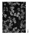
- FIG. 10is a photograph of a plurality of framed symbols within a greater number of flakes absent any covert symbols or frames where a ratio of framed symbols to other flakes is 1:10.
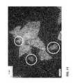
- FIG. 11is a photograph of a plurality of ⁇ symbols some of which are cracked through the symbols and some of which have plural symbols on a single flake; the great distribution in particle size is evidenced here in this photograph due to the absence of providing frames or borders about the symbols.
- FIG. 12is an embodiment in accordance with this invention wherein a flake has color shifting properties, magnetic properties, and bears a covert feature within the flake.
- FIG. 13is a photograph of security features wherein covert flakes are aligned to provide an overt security feature bearing the covert feature within flakes.
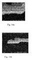
- FIGS. 14 a and 14 bare micro-photographs of a cross section of a flake having a frame with a thinner cross-section in one region as shown.
- FIGS. 15 a , 15 b and 15 care illustrations of flakes having different forms of remnants on more than on edge as a result of a breaking or grinding process.
- Flakes for covert security applicationsare not typically seen by casual observation.
- Some sort of inspection techniquesuch as inspection under a microscope or analytical technique, such as elemental analysis, is used.
- opaque flakes containing indiciasuch as a particular shape, substantially match the visual characteristics of a bulk pigment or other substance they are mixed with.
- a single-layer inorganic opaque flake having a selected shapeis mixed with an iridescent mica-based flake or other base pigment.
- a “single layer” of inorganic materialincludes multiple layers of the same inorganic material built up upon each other.
- bulk pigment particlesincluding bulk pigment flakes
- the covert flakesare distinguishable from bulk pigment flakes by their shape.
- bulk pigment flakeshave a first selected shape, and the covert flakes have a second selected shape.
- Production of shaped pigment flakesis accomplished by a variety of techniques, such as using a patterned substrate to deposit the flake material on the substrate and then separating the flake from the substrate to obtain the pattern such as a frame or border.
- the selected shape of the covert flakesmay be associated with a manufacturing facility, date of manufacture, or other aspect of the document 10 , or ink used in producing the document, for example.
- a roll coateris one type of apparatus that can be used to produce selectively shaped or randomly shaped covert flakes according to embodiments of the invention.
- a roll of a sheet of polymer substrate materialalso known as a “web” is passed through a deposition zone(s) and coated with one or more thin film layers. Multiple passes of the roll of polymer substrate back and forth through the deposition zone(s) may be made. The thin film layer(s) is then separated from the polymer substrate and processed into flake. Other apparatus and techniques may be used.
- PETis one type of polymer film substrate used in roll coaters, and the PET film substrate is usually at least about 13 microns thick. Thinner PET film tends to thermally deform during vacuum deposition processes. Both the heat in the deposition zone and the heat of condensation of the deposited thin-film layer(s) increase the temperature of the polymer substrate as it passes through a deposition zone. Thus, the minimum thickness of flake cut from and incorporating PET film is about 13 microns.
- the covert flakespreferably include a one or more symbols, other forms of indicia within and bordered by the frames, and/or a grating pattern.
- the grating patternis embossed on a substrate used in a roll coater prior to depositing thin film layers that are processed into flakes, or otherwise formed.
- a selected amount (percentage) of the deposition substrate surface areais embossed with a grating pattern or shape pattern to obtain a selected amount of covert flakes when the thin film layers are stripped from the deposition substrate and processed into flakes.
- FIG. 2Bis a simplified view of a portion of another deposition substrate 11 ′ having an embossed portion 13 ′ and a non-embossed portion 15 ′.
- covert pigment flakesare readily identifiable in compositions having 5-10 weight % covert pigment flakes and 95-90 weight % base pigment flakes having similar appearance (e.g. color and/or color travel). Often, shaped opaque covert flakes are easily identifiable in the field using hand-held microscopes (e.g. “shirt-pocket” microscopes), and require less magnification to identify than similar sized flakes having symbols.
- hand-held microscopese.g. “shirt-pocket” microscopes
- “diamond” shaped) bright flake in colored base pigmentscan be added without causing a noticeable change in color, but are still easily identifiable under illuminated magnification of about 50 ⁇ (i.e. 50 times magnification). Under illuminated magnification, both the shape and high brightness of the flake distinguish it from the base flake. When less than about 0.25% of shaped bright flake is used the covert flakes become difficult to detect because dilution with the base flake results in fewer shaped bright flakes in the field of view.
- the base pigment particles 16are illustrated as being irregularly shaped flakes.
- base pigment flakeshave a selected (i.e. regular) shape.
- the covert pigment flake 18could have a grating. The addition of a grating further increases the difficulty of counterfeiting.
- the covert pigment flake 18has generally the same optical characteristics as the base pigment particles.
- the covert pigment flake 18has different optical characteristics as the base pigment particles but is present in sufficiently small quantities so as not to disturb the visual appearance of a composition made with the base pigment particles.
- the “diamond-shaped” covert flakeswere bright flakes about 25 microns by 35 microns across.
- the shaped flakeswere made by embossing a diamond pattern into a roll of PET deposition substrate material, and then depositing a standard thin-film design for bright flake (e.g. about 100-60 nm of Al between layers of MgF 2 that are each about 400 nm thick).
- the total thickness for this bright flakeis about 900 nm, which is about one micron.
- the embossed patternis also known as a “frame” (as opposed to a grating which is intended to produce a pattern in or on the flake), and is positive in some embodiments and negative in other embodiments.
- the diamond-shaped flakesmay be embossed with additional covert symbols, thereby providing two levels of covert features available to protect a device.
- metal-dielectric and dielectric-metal-dielectric flake having a total thickness of between about 0.5 microns and about 3 micronsprovides a good combination of ductile and brittle characteristics that result in good patterning of the flake when it is removed from the substrate and processed.
- shaped bright flake having a total thickness of about one micron of a ductile metal layer between brittle dielectric layersyielded about 90% diamond-shaped flakes from an embossed deposition substrate.
- the base pigment particlesare flakes of mica coated with a layer of TiO 2 or other dielectric material.
- the coating materialtypically has a relatively high index of refraction.
- Micais a naturally occurring mineral that is relatively inexpensive and easily processed into flake substrate.
- a nacreous pigment flakeis obtained.
- Mica flake substratecan be coated with several alternative materials using a variety of processes.
- Such pigmentsare commonly known as “mica-based” pigments. A photocopy of an image printed with such nacreous pigment does not look like the original, thus mica-based pigment flakes are desirable for use to provide overt security features.
- Covert flake according to an embodiment of the present inventionis mixed with the mica-based pigment to enable a covert security feature to be included in images printed with mica-based pigment flakes.
- Shaped pigment flakes made of a single layer of inorganic dielectric material, such as TiO 2 or ZnS,have an appearance similar to a mica-based pigment if the covert pigment flake has a thickness about five times the quarter-wave optical thickness (“QWOT”) at a wavelength in the visible spectrum.
- QWOTquarter-wave optical thickness
- a single-layer covert flake of ZnS intended to match the appearance of a mica-based pigmenthas a thickness of about 60 nm to about 600 nm. Processing all-dielectric flake from a deposition substrate having an embossed diamond-shaped pattern tends to have a lower yield than a counterpart metal-dielectric flake.
- FIG. 3Bis a simplified cross section of a bright pigment flake 20 according to an embodiment of the present invention.
- a reflective layer 22is between two dielectric thin-film layers 24 , 26 .
- the dielectric thin-film layers 24 , 26provide stiffness to the bright pigment flake 20 and facilitate removal of the pigment flake from the roll coater substrate. It is desirable to keep the bright pigment flake less than 10 microns thick to provide a composition that dries or cures to a smooth surface.
- the thickness of the flakeis between about 1 micron and about 3 microns. Thinner flakes tend to be more difficult to process and handle because they weigh so little, and thicker flakes are stronger, and hence more difficult to break along the frame pattern.
- the reflective layer 22is typically a thin-film layer of a highly reflective metal such as aluminum, platinum, gold, silver, or copper, or a moderately reflective metal, such as iron or chromium.
- the reflective layer 22is sufficiently thick to be opaque (reflective) in the visible portion of the spectrum, but not so thick as to interfere with separation of the thin-film layers from the substrate and subsequent processing into flake. In other words, a metal reflective layer that was too thick would provide a ductile layer between the relatively brittle dielectric layers 24 , 26 and tend to interfere with processing the deposited layers into flakes.
- Suitable materials for the dielectric layersinclude ZnS, MgF 2 , SiO 2 , Al 2 O 3 , TiO 2 , Nb 2 O 5 , and Ta 2 O 5 , among others.
- the dielectric thin-film layers 24 , 26also provide environmental protection for the reflective layer 22 .
- FIG. 3Cis a simplified cross section of a bright flake 20 ′ with an elemental indicator layer 28 .
- the bright flake 20 ′has reflective layers 22 ′, 22 ′′ between dielectric layers 24 ′, 26 ′, and a layer 28 providing an elemental indicator.
- the elemental indicator layer 28is a layer of material that is not found in a base pigment that the bright flake will be used with, and that is readily detectable using elemental analysis techniques, such as secondary ion mass spectrometry (“SIMS”), energy dispersive X-ray (“EDX”) and Auger analysis.
- SIMSsecondary ion mass spectrometry
- EDXenergy dispersive X-ray
- Auger analysisAuger analysis.
- the elemental indicatoris present in the covert flake but not in the base flake, and micro-SIMS, micro-EDX or micro-Auger analysis easily detects this difference.
- adding the indicating element to the pigment mixturee.g. adding a small amount of a
- the elemental indicator layer 28is not optically active because it is between the two opaque reflective layers 22 ′, 22 ′′.
- the reflective layers 22 ′, 22 ′′are selected to be of the same material used in the base flake, such as aluminum. Suitable materials for an elemental indicator include platinum, iridium, osmium, vanadium, cobalt, and tungsten, among others. Those of skill in the art appreciate that the elemental indicator material chosen depends on the base pigment it will be used with.
- the reflective layer of bright pigmentis of an elemental indicator material (see FIG. 3B , ref. num. 22 ). For example, covert bright or colored pigment flake using platinum as the reflective layer is mixed with base bright flake or colored pigment flake using aluminum as the reflective layer.
- FIG. 3Dis a simplified cross section of a color-shifting pigment flake 30 according to another embodiment of the present invention.
- the color-shifting pigment flake 30is generally known as a symmetrical 5-layer Fabry-Perot interference flake.
- a thin film stack 32includes a reflective metal layer 34 , two spacer layers 36 A, 36 B, and two absorber layers 38 A, 38 B.
- the absorber layersare typically very thin, semi-opaque layers of chromium, carbon, or other material.
- the reflector, spacer, and absorber layersare all optically active, that is, they contribute to the optical performance of the color-shifting pigment flake.
- the color-shifting pigment flakeis an all-dielectric pigment flake or a 3 layer flake such as an absorber/dielectric/absorber.
- the color and color travel of the color-shifting pigment flakeis determined by the optical design of the flake, namely the material and thicknesses of the layers in the thin film stack 32 , as is well-known in the art of optically variable pigments.
- the optical design of the color-shifting pigment flake 30is typically chosen to match the optical properties of the base pigment flake that it will be mixed with.
- the color-shifting pigment flake 30is shaped (see FIG. 3A , ref num. 18 ), and optionally or alternatively includes other indicia, such as a surface grating pattern and/or elemental indicator.
- the reflective layerincludes an elemental indicator, either a reflective metal that is different than the base pigment flakes, or includes an additional elemental indicator layer(s), which may or may not be optically active (see FIG. 3C , ref num. 28 ).
- the spacer layers 36 A, 36 B and/or the absorber layers 38 A, 38 Binclude an elemental indicator.
- the base pigment flakeuses MgF 2 , SiO 2 , or Al 2 O 3 as a spacer layer material
- the covert pigment flake 30uses different spacer layer material, such as TiO 2 or ZnS. Spacer and/or absorber indicator materials include elements that are easily detected using elemental analysis.
- a different spacer material and/or reflector materialresults in a covert pigment flake 30 that has different optical properties than the base flake. For example, even if the covert and base flakes have similar color at normal incidence, the color travel might be different. Generally, low-index spacer materials (such as MgF 2 and SiO 2 ) provide more color travel (“fast shifting” pigments) than high-index spacer materials (such as ZnS and TiO 2 ). However, such covert flakes can be added in relatively high concentrations to the base pigment flake, even if the color travel does not precisely match that of the base flake, because most casual observers cannot detect the difference between a mixture according to an embodiment of the invention and 100% base flake.
- low-index spacer materialssuch as MgF 2 and SiO 2
- high-index spacer materialssuch as ZnS and TiO 2
- FIG. 4is a cross section of a varnish 40 with covert flakes 42 dispersed in a carrier 44 according to an embodiment of the present invention.
- the carrieris clear or tinted, and the covert flakes 42 are at a concentration selected to avoid casual visual detection.
- An optional color coat or bright (e.g. “chromed”) coating 46has been applied to an object 48 underneath the varnish 40 .
- the varnish 40provides a covert security feature to the object without disturbing its appearance.
- the optional color coat 46is an image printed with nacreous or color-shifting pigment to provide an overt security feature to the object.
- the objectis a document, product, packaging, or seal, for example.
- the varnish 40enables providing a covert security feature to an object that already has a covert security feature without significantly altering the appearance of the object. For example, if stock certificates have been printed with overt security features and it subsequently becomes desirable to provide a covert security feature to the stock certificates, the overt security feature is over-printed with the varnish 40 or a similar ink composition (i.e. an essentially clear ink composition containing covert flakes). In another embodiment, an additional covert security feature is provided to an object already having one or more covert security features. In a particular embodiment, the covert flakes make up not more than 2% of the varnish.
- FIG. 5is a cross section of a composition 50 (e.g. ink or paint) including base pigment flakes 16 and shaped covert flakes 18 dispersed in a binder or carrier 52 according to another embodiment of the present invention.
- the covert flakes 18have a selected shape or other indicia, such as an elemental indicator or a surface grating pattern.
- the composition 50has been applied to an object 48 , such as a label, product packaging, bank note, or consumer item.
- a test standard using 100% magenta-to-green optically variable intaglio (“OVI”) pigment flakewas produced and measured.
- Both bright and optically variable taggent sampleshad a grating pattern of 2000 lines/mm, which made the taggent flakes easier to distinguish from the base pigment flake (i.e. locate) and more difficult to counterfeit.
- the grating patternwas clearly visible at about 400 ⁇ , and did not induce visible diffractive properties to images printed with the test compositions. It is believed that the low portion of the taggent flakes in combination with not being well oriented to the viewer avoided a diffractive effect from occurring.
- a finer grating patternis included on shaped taggent flakes.
- the shapesare identifiable under a microscope at a first magnification, but the grating pattern is not easily seen at this first magnification.
- the grating patternis seen at a higher magnification. It is believed that including such a grating pattern to taggent flake having a selected shape or symbol further enhances the covert nature of the taggent flake because a counterfeiter might see the shape or a symbol under microscopic examination, but not see the grating pattern, and hence not include it in a counterfeit article.
- the first test sample(“sample 1”) contained 90% (by weight) of the conventional (base) magenta-to-green pigment flake mixed with 10% magenta-to-green OVI pigment flake with a grating (“taggent flake”).
- the taggent flakeswere easy to detect by routine microscopic inspection, and the color performance of the mixture was the same as the test standard because the color of the taggent flake was well matched to the color of the base flake. Close color matching involves careful monitoring of the production of the taggent flake and a new optical design for each color of taggent flake would generally be used to match each color of base flake.
- Another approachis to use a standard taggent flake design that can be used with many different colors of base flake.
- Bright taggent flake using an aluminum reflector layergiving the flake a “silver” appearance was also evaluated. Fabrication of bright flake is relatively simple and these flakes were very easy to detect at a concentration of 5% when mixed with colored base pigment flakes.
- Bright taggent flakesare used with many colors of base pigment to provide covet security features. The amount of bright taggent flakes in the composition depends on the desired result.
- the color performance of an intaglio blend containing 5% bright taggent flake mixed with the magenta-to-green OVI baseis distinguishable in a side-by-side comparison from a composition of 100% magenta-to-green OVI flake.
- a composition essentially indistinguishable from 100% magenta-to-green OVI flakeuses less than 5% bright flake, such as compositions with concentrations between about 0.25 weight % and 3 weight % of bright taggent flake in magenta-to-green OVI flake. It is believed that bright flake in concentrations greater than 5% may be added to pigment flake providing lighter or less saturated color without noticeably changing the appearance of the composition.
- Bright taggent flakesare easy to detect under modest magnification, even at concentrations below 1%, because of the combination of having a selected shape and of being a different color (e.g. “silver” instead of magenta).
- FIG. 6is a flow chart of a method 600 of making pigment flake according to an embodiment of the present invention.
- a roll substrate having a non-embossed (“smooth”) portion and an embossed portion in a selected ratio of the deposition surface area of the roll substrateis provided (step 602 ).
- the embossed portionis embossed with a frame for producing flakes having a selected shape.
- the embossed portionis embossed with a grating pattern or symbol.
- the substrateis patterned using a process other than embossing, such as laser ablation.
- At least one thin film layeris deposited on the roll substrate (step 604 ), and the deposited thin film layer(s) is processed into flake (step 606 ) to result in a flake mixture having a selected amount of taggent flakes.
- the yield of taggent flakedepends on factors such as the type of thin-film layers being processed, the nature of the frame, grating pattern, or symbol, and processing parameters.
- a yield of approximately 10% taggent flake having the grating pattern or symbolis expected. If 10% of the surface of the roll substrate is embossed with a diamond-shaped frame, then a yield of about 9% is expected for dielectric-metal-dielectric flake because of the 10% yield loss processing the patterned portion of the thin film stack into shaped flakes. Similarly, a yield of about 5% is expected for shaped all-dielectric flake because of the 50% yield loss processing the patterned portion of the thin film stack into shaped flakes.
- an embodiment of this inventionwhich offers significant advantages is the aspect of using frames or borders framing symbols or indicia framed by these borders on a substrate material used to form a coating upon.
- FIG. 7a photograph is shown of sheet bearing a plurality of Euro symbols wherein each symbol on the sheet has an embossed border around it. This is generally accomplished by embossing an organic substrate, such as a PET substrate with the framed symbols, and subsequently coating the substrate with a removable coating.
- FIG. 8is a photograph of the flakes after separation from their backing or substrate. This photograph clearly shows most of the symbols to be intact with few cracks appearing into or through the symbols. By using this invention, a very small portion of the flakes in the figure are broken in such a manner as to obscure the symbol. However what is shown is that the frames are not present along all sides of all flakes after the flakes break apart from the substrate they were deposited on.
- flakeshave no borders and others may have one and up to four borders. However, this is understandable. Since a frame border separates the flake from its nearest neighbour, when the flakes separate the border generally remains attached to one flake an not its adjacent flake on the other side of that frame border. However the existence of the frame or border results in most of the flakes breaking upon frame lines, on one side of the frame or the other providing relatively uniform flakes with relatively straight edges. More often than not, each flake bearing a symbol will have at least one border or frame segment attached to it after separating from the web or substrate it was deposited on.
- FIGS. 7 to 13were filed in color as part of U.S. Ser. No. 11/243,122 filed Oct. 4, 2005, now issued as U.S. Pat. No. 7,645,510, of which the present application claims priority.
- FIG. 9is a photograph of a plurality of Mg-Gn flakes bearing ⁇ symbols wherein the flakes have broken randomly preserving some symbols and destroying others, due to stress cracks and resulting apparently random fracture lines as a result of the absence of frames.
- FIG. 9illustrates stress cracks throughout the flakes causing the flakes to separate as a function of these cracks. Furthermore, cracks continue to appear within flakes thereby obscuring symbols.
- the provision of frames in accordance with this inventiondoes not entirely prevent stress cracks, however provides a means in which these cracks can be controlled to a greater extent, so as to occur or be preferentially routed along the frame lines.
- the embodiment of this invention shown in conjunction with FIGS. 7 and 8offers a manner in which the flakes can be separated along predetermined borders thereby preserving the shape and integrity of the symbols on the flakes to a much higher degree and generally does obscure the covert symbol within the flake.
- the cracks that do appear in the non-framed symbolsappear and propagate in the more fragile, glass-like, dielectric material but are stopped and rerouted to continue their propagation along the frame lines provided in the sheet of framed symbols shown in FIG. 7 .
- the provision of framesproduces the preferential rupture of the flakes along frame lines.
- Most of the cracks observed in the flakes of FIG. 8do not go all the way through the total thickness of the flakes, but are stopped at the level of the more elastic metallic core (Al/Ni/Al) of the flakes producing a shadowing effect detrimental to the readability of the originally embossed symbols.
- the flakes in both FIGS. 8 and 9are about 1300 nm or 1.3 microns in thickness and have a layer structure of 10 nm Cr/480 nm MgF2/80 nm Al/50 nm Ni/80 nm Al 480 nm MgF2/10 nm Cr. Ni is present to provide the magnetic layer for overt features.
- FIG. 10is a photograph of a plurality of framed symbols within a greater number of flakes absent any covert symbols or frames where a ratio of framed symbols to other flakes is 1:10.
- a ratio of framed symbols to other flakesis 1:10.
- On a first level of detectionone, equipped with a 100 ⁇ hand held microscope can detect the presence of covert flakes with a Euro symbol thereon, and furthermore, one can also quickly approximate that the ratio of covert to non-covert symbols is about 1:10. Yet still further, one can compare the ratio of square symbols to randomly shaped flakes to provide some measure of authentication. Therefore, shape, distribution, and identification of the symbols within framed shapes can be used to determine if the coating is authentic within some range of assurance.
- FIG. 11is a close-up detailed photograph of a plurality of ⁇ symbols some of which are cracked through the symbols and some of which have plural symbols on a single flake; the great distribution in particle size is evidenced here in this photograph due to the absence of providing frames or borders about the symbols.
- FIG. 12illustrates an embodiment in accordance with this invention wherein a flake has color shifting properties, magnetic properties, and bears a covert feature within the flake.
- the flakeis also bordered by a frame to preserve its shape.
- FIG. 12a pigment flake is shown having a magnetic layer sandwiched between two aluminum reflective layers.
- Each of the aluminum layersin addition to an absorber and dielectric layer provide color shifting layers on each side.
- Within the flakeis stamped a covert “euro” symbol thereon which can be seen with suitable magnification.
- the embodiment shown in FIG. 13utilizes a plurality of the flakes shown in FIG. 12 to provide a security features that are both covert and overt.
- the covert and overt featuresare illustrated in the photograph which is a compilation of 3 photographs depicted by FIG. 13 where a large Euro symbol and a map of the continents are shown on the upper right in the photograph and wherein a globe is shown on the upper left of the photograph printed by silk screen in the presence of magnetic fields to create different visual contrasts (rolling bar effect) in addition to the standard green to magenta color shifting.
- covert framed square flakes of about 30 microns in sizebear a Euro symbol about 17 microns across.
- optically variable, special magnetically alignable, and covert featurecan be provided within a same security device.
- FIGS. 14 a and 14 ba cross section of a flake having a frame is shown wherein a thinner region with a bend has a thinner cross-section than the rest of the flake.
- the flaketends to break where the cross-section is thinner than the average cross-section of the flake, as this thinner region facilitates breakage.
- shaped flakescan be made by other methods that are similar in one respect to the provision of frames, but which provide useful manufacturing alternatives.
- U.S. patent application Ser. No. 11/931,816 now published U.S. Application 20080107856 from which this application claims priorityteaches the provision of forming a substrate or stamping a substrate so as to be frameless but to have walls which facilitate flakes breaking along predetermined boundaries.
- U.S. patent application Ser. No. 12/463,114 now published U.S. Application 20090217842 from which this application claims priorityteaches the provision of a stamped substrate that has a postage-stamp like embossing that facilitates breakage of the flake along predetermined boundaries.
- the selected shaped flakesare recognizable as being a same selected shape, however upon closer inspection and with significantly higher magnification, differences are seen along edges of different flakes, and often even edges of the same flake vary from one another. Due to the thinning of the edge, and forces applied in breaking the flakes, the break lines may appear slightly jagged or have a cleaved appearance. In almost all cases there will also be a remnant of a wall remaining.
- FIG. 15a substantially planar flakes having at least one planar side are show, wherein a flake has remnants 150 a of a frame shown along two edges.
- a flakehas remnants 150 a of a frame shown along two edges.
- the provisional of a framefacilitates breakage. Notwithstanding, due to the grinding and breaking process almost all shaped flakes will have some remnants of the frame wall.
- a remnant 150 bis shown in the form of an upstanding wall that was provided to facilitate breakage of the flake about or along the wall edge.
- the breakage of the coating on the substratewill provide shaped flakes of a preselected shape, however in most instances there will be one or more remnants of a wall along one or more edges of the flake.
- 15 cillustrates a shaped flake that was made using the postage-stamp method described heretofore.
- a remnant of a wall 150 cis present along two edges, as shown. Fortunately, these remnants are so small, that when just enough magnification is used to see the shaped flake, these remnants are barely visible and don't significantly detract from the appearance of the shaped flake. Since the remnants are of different forms, depending on the particular feature provided to facilitate breakage, one can identify the flakes in accordance with the feature. For example another way in which security is added to the flake, is that one can identify if it was made by using frames, or walls or the postage stamp like feature to facilitate breakage. These remnants form a type of recognizable signature.
Landscapes
- Physics & Mathematics (AREA)
- General Physics & Mathematics (AREA)
- Chemical & Material Sciences (AREA)
- Inorganic Chemistry (AREA)
- Spectroscopy & Molecular Physics (AREA)
- Organic Chemistry (AREA)
- Crystallography & Structural Chemistry (AREA)
- Engineering & Computer Science (AREA)
- Wood Science & Technology (AREA)
- Materials Engineering (AREA)
- Life Sciences & Earth Sciences (AREA)
- Developing Agents For Electrophotography (AREA)
- Inks, Pencil-Leads, Or Crayons (AREA)
- Pigments, Carbon Blacks, Or Wood Stains (AREA)
- Cleaning In Electrography (AREA)
- Thermal Transfer Or Thermal Recording In General (AREA)
Abstract
Description

Claims (22)
Priority Applications (1)
| Application Number | Priority Date | Filing Date | Title |
|---|---|---|---|
| US14/151,511US8999616B2 (en) | 2002-09-13 | 2014-01-09 | Taggent flakes for covert security applications having a selected shape |
Applications Claiming Priority (14)
| Application Number | Priority Date | Filing Date | Title |
|---|---|---|---|
| US10/243,111US6902807B1 (en) | 2002-09-13 | 2002-09-13 | Alignable diffractive pigment flakes |
| US10/641,695US7258915B2 (en) | 2003-08-14 | 2003-08-14 | Flake for covert security applications |
| US10/762,158US7241489B2 (en) | 2002-09-13 | 2004-01-20 | Opaque flake for covert security applications |
| US69659305P | 2005-07-05 | 2005-07-05 | |
| US11/243,122US7645510B2 (en) | 2002-09-13 | 2005-10-04 | Provision of frames or borders around opaque flakes for covert security applications |
| US11/931,816US9164575B2 (en) | 2002-09-13 | 2007-10-31 | Provision of frames or borders around pigment flakes for covert security applications |
| US2844208P | 2008-02-13 | 2008-02-13 | |
| US5146308P | 2008-05-08 | 2008-05-08 | |
| US12/378,371US20090202932A1 (en) | 2008-02-13 | 2009-02-13 | Medium for laser printing including optical special effect flakes |
| US12/463,114US9458324B2 (en) | 2002-09-13 | 2009-05-08 | Flakes with undulate borders and method of forming thereof |
| US25766409P | 2009-11-03 | 2009-11-03 | |
| US12/938,304US8323542B2 (en) | 2009-11-03 | 2010-11-02 | Substrate and method of manufacturing polygon flakes |
| US13/284,689US8658280B2 (en) | 2002-09-13 | 2011-10-28 | Taggent flakes for covert security applications having a selected shape |
| US14/151,511US8999616B2 (en) | 2002-09-13 | 2014-01-09 | Taggent flakes for covert security applications having a selected shape |
Related Parent Applications (1)
| Application Number | Title | Priority Date | Filing Date |
|---|---|---|---|
| US13/284,689DivisionUS8658280B2 (en) | 2002-09-13 | 2011-10-28 | Taggent flakes for covert security applications having a selected shape |
Publications (2)
| Publication Number | Publication Date |
|---|---|
| US20140127622A1 US20140127622A1 (en) | 2014-05-08 |
| US8999616B2true US8999616B2 (en) | 2015-04-07 |
Family
ID=40718756
Family Applications (3)
| Application Number | Title | Priority Date | Filing Date |
|---|---|---|---|
| US12/378,371AbandonedUS20090202932A1 (en) | 2002-09-13 | 2009-02-13 | Medium for laser printing including optical special effect flakes |
| US13/284,689Expired - LifetimeUS8658280B2 (en) | 2002-09-13 | 2011-10-28 | Taggent flakes for covert security applications having a selected shape |
| US14/151,511Expired - LifetimeUS8999616B2 (en) | 2002-09-13 | 2014-01-09 | Taggent flakes for covert security applications having a selected shape |
Family Applications Before (2)
| Application Number | Title | Priority Date | Filing Date |
|---|---|---|---|
| US12/378,371AbandonedUS20090202932A1 (en) | 2002-09-13 | 2009-02-13 | Medium for laser printing including optical special effect flakes |
| US13/284,689Expired - LifetimeUS8658280B2 (en) | 2002-09-13 | 2011-10-28 | Taggent flakes for covert security applications having a selected shape |
Country Status (4)
| Country | Link |
|---|---|
| US (3) | US20090202932A1 (en) |
| EP (1) | EP2090935A1 (en) |
| JP (1) | JP2009193069A (en) |
| CN (1) | CN101515124A (en) |
Families Citing this family (25)
| Publication number | Priority date | Publication date | Assignee | Title |
|---|---|---|---|---|
| WO2012011323A1 (en)* | 2010-07-23 | 2012-01-26 | 日本電気株式会社 | Laser light source module |
| JP2012121173A (en)* | 2010-12-06 | 2012-06-28 | Dainippon Printing Co Ltd | Taggant particle group, anti-counterfeit ink comprising the same, anti-counterfeit toner, anti-counterfeit sheet, and anti-counterfeit medium |
| JP5589939B2 (en) | 2011-04-12 | 2014-09-17 | 大日本印刷株式会社 | Fine particles, particle group, anti-counterfeit ink, anti-counterfeit toner, anti-counterfeit sheet and anti-counterfeit medium |
| JP5824878B2 (en)* | 2011-05-31 | 2015-12-02 | 大日本印刷株式会社 | Method for producing anti-counterfeit particles |
| JP5729140B2 (en)* | 2011-05-31 | 2015-06-03 | 大日本印刷株式会社 | Method for producing anti-counterfeit resin particles, method for producing anti-counterfeit ink, method for producing anti-counterfeit sheet |
| KR101857160B1 (en)* | 2011-12-16 | 2018-05-15 | 한국전자통신연구원 | Semiconductor LASER and method of fabricating the same |
| JP6312664B2 (en)* | 2012-06-26 | 2018-04-18 | ケーエルエー−テンカー コーポレイション | Near field measurement |
| JP5532172B1 (en)* | 2013-06-03 | 2014-06-25 | 富士ゼロックス株式会社 | Image forming apparatus |
| TWI641660B (en)* | 2013-08-05 | 2018-11-21 | 瑞士商西克帕控股有限公司 | Magnetic or magnetizable pigment particles and optical effect layers |
| FR3016054B1 (en)* | 2013-12-27 | 2017-05-19 | Oreal | COSMETIC LASER PRINTER |
| FR3015872B1 (en) | 2013-12-27 | 2017-03-24 | Oreal | MAKE-UP DEVICE COMPRISING A PLURALITY OF COSMETIC INKS |
| FR3015889B1 (en) | 2013-12-27 | 2016-02-05 | Oreal | DEVICE FOR MAKE-UP BY TRANSFERRING KERATINIC MATERIALS |
| FR3015887B1 (en) | 2013-12-27 | 2017-03-24 | Oreal | DEVICE AND METHOD FOR MAKE-UP BY TRANSFERRING KERATINIC MATERIALS |
| FR3015870B1 (en) | 2013-12-27 | 2016-02-05 | Oreal | DEVICE FOR MAKE-UP BY TRANSFERRING KERATINIC MATERIALS. |
| FR3015890B1 (en) | 2013-12-27 | 2016-02-05 | Oreal | DEVICE FOR MAKE-UP BY TRANSFERRING KERATINIC MATERIALS |
| FR3015927A1 (en) | 2013-12-27 | 2015-07-03 | Oreal | TRANSFER MAKEUP METHOD AND ASSOCIATED DEVICE. |
| FR3015888B1 (en) | 2013-12-27 | 2017-03-31 | Oreal | DEVICE FOR MAKE-UP BY TRANSFERRING KERATINIC MATERIALS |
| EP2993208A1 (en)* | 2014-09-08 | 2016-03-09 | Constantia Flexibles International GmbH | Varnish |
| JP5880653B2 (en)* | 2014-09-29 | 2016-03-09 | 大日本印刷株式会社 | Method for producing fine particle-containing sheet |
| US9628662B1 (en) | 2015-10-15 | 2017-04-18 | Xerox Corporation | Security feature in graphic documents |
| FR3059897B1 (en) | 2016-12-09 | 2019-05-24 | L'oreal | PROCESS FOR PRODUCING A COSMETIC ARTICLE |
| US10642179B2 (en)* | 2018-01-24 | 2020-05-05 | Xerox Corporation | Security toner and process using thereof |
| US10495996B1 (en)* | 2018-10-02 | 2019-12-03 | Xerox Corporation | Surface additive infrared taggant toner |
| JPWO2024009703A1 (en) | 2022-07-08 | 2024-01-11 | ||
| AR130228A1 (en) | 2022-08-23 | 2024-11-20 | Sicpa Holding Sa | SECURITY INK COMPOSITION AND MACHINE-READABLE SECURITY FEATURE DERIVED THEREFROM |
Citations (198)
| Publication number | Priority date | Publication date | Assignee | Title |
|---|---|---|---|---|
| US2570856A (en) | 1947-03-25 | 1951-10-09 | Du Pont | Process for obtaining pigmented films |
| DE1696245U (en) | 1955-02-14 | 1955-04-07 | Willy Bucke | LETTER CLIP. |
| US3011383A (en) | 1957-04-30 | 1961-12-05 | Carpenter L E Co | Decorative optical material |
| US3123490A (en) | 1961-05-04 | 1964-03-03 | Nacreous pigment and method for preparing same | |
| US3338730A (en) | 1964-02-18 | 1967-08-29 | Little Inc A | Method of treating reflective surfaces to make them multihued and resulting product |
| GB1107395A (en) | 1964-06-05 | 1968-03-27 | Agfa Ag | Printing method and rotary duplicator for use therein |
| GB1131038A (en) | 1965-04-15 | 1968-10-16 | Tefal Sa | Procedure for producing a pattern of particles in a polytetrafluoroethylene matrix |
| US3610721A (en) | 1969-10-29 | 1971-10-05 | Du Pont | Magnetic holograms |
| US3627580A (en) | 1969-02-24 | 1971-12-14 | Eastman Kodak Co | Manufacture of magnetically sensitized webs |
| US3633720A (en) | 1969-09-25 | 1972-01-11 | Honeywell Inc | Alphanumeric printing device employing magnetically positionable particles |
| US3676273A (en) | 1970-07-30 | 1972-07-11 | Du Pont | Films containing superimposed curved configurations of magnetically orientated pigment |
| US3790407A (en) | 1970-12-28 | 1974-02-05 | Ibm | Recording media and method of making |
| US3791864A (en) | 1970-11-07 | 1974-02-12 | Magnetfab Bonn Gmbh | Method of ornamenting articles by means of magnetically oriented particles |
| US3845499A (en) | 1969-09-25 | 1974-10-29 | Honeywell Inc | Apparatus for orienting magnetic particles having a fixed and varying magnetic field component |
| US3853676A (en) | 1970-07-30 | 1974-12-10 | Du Pont | Reference points on films containing curved configurations of magnetically oriented pigment |
| US3873975A (en) | 1973-05-02 | 1975-03-25 | Minnesota Mining & Mfg | System and method for authenticating and interrogating a magnetic record medium |
| AU488652B2 (en) | 1973-09-26 | 1976-04-01 | Commonwealth Scientific And Industrial Research Organisation | Improvements in or relating to security tokens |
| US4011009A (en) | 1975-05-27 | 1977-03-08 | Xerox Corporation | Reflection diffraction grating having a controllable blaze angle |
| US4053433A (en) | 1975-02-19 | 1977-10-11 | Minnesota Mining And Manufacturing Company | Method of tagging with color-coded microparticles |
| US4054922A (en) | 1975-05-09 | 1977-10-18 | Kienzle Apparate Gmbh | Apparatus for forming an erasable record of the value of a measured quantity |
| US4066280A (en) | 1976-06-08 | 1978-01-03 | American Bank Note Company | Documents of value printed to prevent counterfeiting |
| US4099838A (en) | 1976-06-07 | 1978-07-11 | Minnesota Mining And Manufacturing Company | Reflective sheet material |
| US4126373A (en) | 1975-12-22 | 1978-11-21 | Hoechst Aktiengesellschaft | Holographic identification elements and method and apparatus for manufacture thereof |
| US4155627A (en) | 1976-02-02 | 1979-05-22 | Rca Corporation | Color diffractive subtractive filter master recording comprising a plurality of superposed two-level relief patterns on the surface of a substrate |
| US4168983A (en) | 1978-04-13 | 1979-09-25 | Vittands Walter A | Phosphate coating composition |
| US4174170A (en) | 1976-12-16 | 1979-11-13 | Minolta Camera Kabushiki Kaisha | Conductive toner transfer photocopying machine |
| US4197563A (en) | 1977-11-10 | 1980-04-08 | Transac - Compagnie Pour Le Developpement Des Transactions Automatiques | Method and device for orientating and fixing in a determined direction magnetic particles contained in a polymerizable ink |
| US4244998A (en) | 1976-12-06 | 1981-01-13 | E M I Limited | Patterned layers including magnetizable material |
| US4271782A (en) | 1978-06-05 | 1981-06-09 | International Business Machines Corporation | Apparatus for disorienting magnetic particles |
| US4310584A (en) | 1979-12-26 | 1982-01-12 | The Mearl Corporation | Multilayer light-reflecting film |
| US4394477A (en) | 1980-10-30 | 1983-07-19 | Screeton James B | Coating composition |
| US4398798A (en) | 1980-12-18 | 1983-08-16 | Sperry Corporation | Image rotating diffraction grating |
| US4434010A (en) | 1979-12-28 | 1984-02-28 | Optical Coating Laboratory, Inc. | Article and method for forming thin film flakes and coatings |
| US4543551A (en) | 1984-07-02 | 1985-09-24 | Polaroid Corporation | Apparatus for orienting magnetic particles in recording media |
| US4652395A (en) | 1985-10-21 | 1987-03-24 | The W. W. Henry Company | Taggant composition |
| US4685793A (en) | 1984-07-26 | 1987-08-11 | Canon Kabushiki Kaisha | Image forming apparatus |
| US4705300A (en) | 1984-07-13 | 1987-11-10 | Optical Coating Laboratory, Inc. | Thin film optically variable article and method having gold to green color shift for currency authentication |
| US4705356A (en) | 1984-07-13 | 1987-11-10 | Optical Coating Laboratory, Inc. | Thin film optical variable article having substantial color shift with angle and method |
| US4721217A (en) | 1986-08-07 | 1988-01-26 | Optical Coating Laboratory, Inc. | Tamper evident optically variable device and article utilizing the same |
| US4756771A (en) | 1985-01-03 | 1988-07-12 | Henkel Kommanditgesellschaft Auf Aktien | Colorless sealing layers for anodized aluminum surfaces |
| WO1988007214A1 (en) | 1987-03-10 | 1988-09-22 | Precis (549) Limited | Light reflective materials |
| US4779898A (en) | 1986-11-21 | 1988-10-25 | Optical Coating Laboratory, Inc. | Thin film optically variable article and method having gold to green color shift for currency authentication |
| EP0138194B1 (en) | 1983-10-14 | 1988-11-09 | The Dow Chemical Company | Coextruded multi-layered articles |
| JPS63172279U (en) | 1987-04-27 | 1988-11-09 | ||
| US4788116A (en) | 1986-03-31 | 1988-11-29 | Xerox Corporation | Full color images using multiple diffraction gratings and masking techniques |
| US4838648A (en) | 1988-05-03 | 1989-06-13 | Optical Coating Laboratory, Inc. | Thin film structure having magnetic and color shifting properties |
| US4847652A (en) | 1986-09-19 | 1989-07-11 | Sharp Kabushiki Kaisha | Image transfer device |
| US4867793A (en) | 1986-05-23 | 1989-09-19 | Merck Patent Gesellschaft Mit Beschrankter Haftung | Nacreous pigments |
| US4930866A (en) | 1986-11-21 | 1990-06-05 | Flex Products, Inc. | Thin film optical variable article and method having gold to green color shift for currency authentication |
| US4931309A (en) | 1988-01-18 | 1990-06-05 | Fuji Photo Film Co., Ltd. | Method and apparatus for producing magnetic recording medium |
| EP0185396B1 (en) | 1984-12-21 | 1990-08-08 | GAO Gesellschaft für Automation und Organisation mbH | Security document incorporating a security thread, and process for manufacturing and checking the authenticity of the security document |
| US5002312A (en) | 1988-05-03 | 1991-03-26 | Flex Products, Inc. | Pre-imaged high resolution hot stamp transfer foil, article and method |
| US5009486A (en) | 1984-06-08 | 1991-04-23 | Canadian Patents And Development Limited/Societe Canadienne Des Brevets Et D'exploitation Limitee | Form depicting, optical interference authenticating device |
| US5059245A (en) | 1979-12-28 | 1991-10-22 | Flex Products, Inc. | Ink incorporating optically variable thin film flakes |
| US5079058A (en) | 1989-03-03 | 1992-01-07 | Kansai Paint Co., Ltd. | Patterned film forming laminated sheet |
| US5079085A (en) | 1988-10-05 | 1992-01-07 | Fuji Photo Film Co., Ltd. | Magnetic recording medium containing a binder which is chemically bonded to crosslinked resin fine particles contained in the magnetic layer |
| US5084351A (en) | 1979-12-28 | 1992-01-28 | Flex Products, Inc. | Optically variable multilayer thin film interference stack on flexible insoluble web |
| US5106125A (en) | 1989-12-01 | 1992-04-21 | Landis & Gyr Betriebs Ag | Arrangement to improve forgery protection of credit documents |
| EP0453131A3 (en) | 1990-04-12 | 1992-04-29 | James River Corporation | Security paper and method of manufacturing same |
| US5128779A (en) | 1988-02-12 | 1992-07-07 | American Banknote Holographics, Inc. | Non-continuous holograms, methods of making them and articles incorporating them |
| US5135812A (en) | 1979-12-28 | 1992-08-04 | Flex Products, Inc. | Optically variable thin film flake and collection of the same |
| US5142383A (en) | 1990-01-25 | 1992-08-25 | American Banknote Holographics, Inc. | Holograms with discontinuous metallization including alpha-numeric shapes |
| US5171363A (en) | 1979-12-28 | 1992-12-15 | Flex Products, Inc. | Optically variable printing ink |
| US5177344A (en) | 1990-10-05 | 1993-01-05 | Rand Mcnally & Company | Method and appparatus for enhancing a randomly varying security characteristic |
| US5186787A (en) | 1988-05-03 | 1993-02-16 | Phillips Roger W | Pre-imaged high resolution hot stamp transfer foil, article and method |
| US5192611A (en) | 1989-03-03 | 1993-03-09 | Kansai Paint Co., Ltd. | Patterned film forming laminated sheet |
| US5208630A (en) | 1991-11-04 | 1993-05-04 | Xerox Corporation | Process for the authentication of documents utilizing encapsulated toners |
| US5214530A (en) | 1990-08-16 | 1993-05-25 | Flex Products, Inc. | Optically variable interference device with peak suppression and method |
| US5223360A (en) | 1989-11-16 | 1993-06-29 | Merck Patent Gesellschaft Mit Beschrankter Haftung | Materials coated with plate-like pigments |
| US5254390A (en) | 1990-11-15 | 1993-10-19 | Minnesota Mining And Manufacturing Company | Plano-convex base sheet for retroreflective articles and method for making same |
| WO1993023251A1 (en) | 1992-05-11 | 1993-11-25 | Avery Dennison Corporation | Method of enhancing the visibility of diffraction pattern surface embossment |
| US5278590A (en) | 1989-04-26 | 1994-01-11 | Flex Products, Inc. | Transparent optically variable device |
| US5339737A (en) | 1992-07-20 | 1994-08-23 | Presstek, Inc. | Lithographic printing plates for use with laser-discharge imaging apparatus |
| US5354374A (en) | 1991-11-16 | 1994-10-11 | Merck Patent Gesellschaft Mit Beschrankter Haftung | Iron oxide pigments |
| US5364467A (en) | 1992-05-27 | 1994-11-15 | Basf Aktiengesellschaft | Luster pigments based on multiply coated plateletlike metalic substrates |
| US5364689A (en) | 1992-02-21 | 1994-11-15 | Hashimoto Forming Industry Co., Ltd. | Painting with magnetically formed pattern and painted product with magnetically formed pattern |
| US5368898A (en) | 1992-09-09 | 1994-11-29 | Agency Of Industrial Science & Technology | Method of generating micro-topography on a surface |
| EP0406667B1 (en) | 1989-06-27 | 1995-01-11 | Nippon Paint Co., Ltd. | Forming method of patterned coating |
| US5411296A (en) | 1988-02-12 | 1995-05-02 | American Banknote Holographics, Inc. | Non-continuous holograms, methods of making them and articles incorporating them |
| WO1995013569A1 (en) | 1993-11-08 | 1995-05-18 | E.I. Du Pont De Nemours And Company | Holographic flake pigment |
| US5424119A (en) | 1994-02-04 | 1995-06-13 | Flex Products, Inc. | Polymeric sheet having oriented multilayer interference thin film flakes therein, product using the same and method |
| DE4343387A1 (en) | 1993-12-18 | 1995-06-29 | Kurz Leonhard Fa | Visually identifiable, optical security element for documents of value |
| WO1995017475A1 (en) | 1993-12-23 | 1995-06-29 | Basf Corporation | Coating composition containing optically-variable dichroic pigment and interference mica pigment |
| US5437931A (en) | 1993-10-20 | 1995-08-01 | Industrial Technology Research Institute | Optically variable multilayer film and optically variable pigment obtained therefrom |
| US5447335A (en) | 1990-11-22 | 1995-09-05 | Thomas De La Rue Limited | Security device and authenticatable item |
| US5464710A (en) | 1993-12-10 | 1995-11-07 | Deposition Technologies, Inc. | Enhancement of optically variable images |
| US5474814A (en) | 1992-03-13 | 1995-12-12 | Fuji Photo Film Co., Ltd. | Magnetic recording medium and method for producing the same |
| EP0710508A1 (en) | 1994-11-04 | 1996-05-08 | Basf Aktiengesellschaft | Process for making coatings having three dimensional optical effects |
| DE4212290C2 (en) | 1992-02-29 | 1996-08-01 | Kurz Leonhard Fa | value document |
| US5549953A (en) | 1993-04-29 | 1996-08-27 | National Research Council Of Canada | Optical recording media having optically-variable security properties |
| US5571624A (en) | 1979-12-28 | 1996-11-05 | Flex Products, Inc. | High chroma multilayer interference platelets |
| US5591527A (en) | 1994-11-02 | 1997-01-07 | Minnesota Mining And Manufacturing Company | Optical security articles and methods for making same |
| EP0756945A1 (en) | 1995-07-31 | 1997-02-05 | National Bank Of Belgium | Colour copy protection of security documents |
| US5613022A (en) | 1993-07-16 | 1997-03-18 | Luckoff Display Corporation | Diffractive display and method utilizing reflective or transmissive light yielding single pixel full color capability |
| US5624076A (en) | 1992-05-11 | 1997-04-29 | Avery Dennison Corporation | Process for making embossed metallic leafing pigments |
| US5627663A (en) | 1993-08-31 | 1997-05-06 | Control Module Inc. | Secure optical identification method and means |
| USRE35512E (en) | 1992-07-20 | 1997-05-20 | Presstek, Inc. | Lithographic printing members for use with laser-discharge imaging |
| WO1997019820A1 (en) | 1995-11-28 | 1997-06-05 | Electrowatt Technology Innovation Ag | Optical information carrier |
| US5653792A (en) | 1979-12-28 | 1997-08-05 | Flex Products, Inc. | Optically variable flakes paint and article |
| DE19611383A1 (en) | 1996-03-22 | 1997-09-25 | Giesecke & Devrient Gmbh | Data carrier with optically variable element |
| US5700550A (en) | 1993-12-27 | 1997-12-23 | Toppan Printing Co., Ltd. | Transparent hologram seal |
| WO1998012583A1 (en) | 1996-09-23 | 1998-03-26 | The Secretary Of State For Defence | Multi layer interference coatings |
| US5742411A (en) | 1996-04-23 | 1998-04-21 | Advanced Deposition Technologies, Inc. | Security hologram with covert messaging |
| US5744223A (en) | 1993-10-16 | 1998-04-28 | Mercedes Benz Ag | Marking of vehicles to hinder theft and/or unauthorized sale |
| US5753392A (en) | 1995-08-24 | 1998-05-19 | Minnesota Mining And Manufacturing Company | Method of electrostatically printing image-enhancing particles and said particles |
| US5763086A (en) | 1995-10-14 | 1998-06-09 | Basf Aktiengesellschaft | Goniochromatic luster pigments with silicon-containing coating |
| US5811775A (en) | 1993-04-06 | 1998-09-22 | Commonwealth Scientific And Industrial Research Organisation | Optical data element including a diffraction zone with a multiplicity of diffraction gratings |
| US5815292A (en) | 1996-02-21 | 1998-09-29 | Advanced Deposition Technologies, Inc. | Low cost diffraction images for high security application |
| US5814367A (en) | 1993-08-13 | 1998-09-29 | General Atomics | Broadband infrared and signature control materials and methods of producing the same |
| US5856048A (en) | 1992-07-27 | 1999-01-05 | Dai Nippon Printing Co., Ltd. | Information-recorded media and methods for reading the information |
| US5858078A (en) | 1996-05-09 | 1999-01-12 | Merck Patent Gesellschaft Mit Beschrankter Haftung | Platelet-shaped titanium dioxide pigment |
| JPH1110771A (en) | 1997-06-20 | 1999-01-19 | Toppan Printing Co Ltd | Forgery prevention film and forgery prevention transfer foil |
| DE19731968A1 (en) | 1997-07-24 | 1999-01-28 | Giesecke & Devrient Gmbh | Security document |
| EP0420261B1 (en) | 1989-09-28 | 1999-03-24 | GAO Gesellschaft für Automation und Organisation mbH | Record carrier with an optical variable element and method of producing it |
| DE19744953A1 (en) | 1997-10-10 | 1999-04-15 | Giesecke & Devrient Gmbh | Security element with an auxiliary inorganic layer |
| US5907436A (en) | 1995-09-29 | 1999-05-25 | The Regents Of The University Of California | Multilayer dielectric diffraction gratings |
| US5912767A (en) | 1993-11-23 | 1999-06-15 | Commonwealth Scientific And Industrial Research Organisation | Diffractive indicia for a surface |
| EP0953937A1 (en) | 1998-04-30 | 1999-11-03 | Securency Pty. Ltd. | Security element to prevent counterfeiting of value documents |
| US5989626A (en) | 1995-05-09 | 1999-11-23 | Flex Products, Inc. | Mixed oxide high index optical coating material and method |
| US5991078A (en) | 1992-08-19 | 1999-11-23 | Dai Nippon Printing Co., Ltd. | Display medium employing diffraction grating and method of producing diffraction grating assembly |
| US6013370A (en) | 1998-01-09 | 2000-01-11 | Flex Products, Inc. | Bright metal flake |
| WO2000008596A1 (en) | 1998-08-06 | 2000-02-17 | Sicpa Holding S.A. | Inorganic sheet carrying symbols for making pigments |
| US6031457A (en) | 1998-06-09 | 2000-02-29 | Flex Products, Inc. | Conductive security article and method of manufacture |
| US6033782A (en) | 1993-08-13 | 2000-03-07 | General Atomics | Low volume lightweight magnetodielectric materials |
| US6043936A (en) | 1995-12-06 | 2000-03-28 | De La Rue International Limited | Diffractive structure on inclined facets |
| US6045230A (en) | 1998-02-05 | 2000-04-04 | 3M Innovative Properties Company | Modulating retroreflective article |
| US6071665A (en) | 1995-05-26 | 2000-06-06 | Xerox Corporation | Toner processes with surface additives |
| US6103361A (en) | 1997-09-08 | 2000-08-15 | E. I. Du Pont De Nemours And Company | Patterned release finish |
| US6112388A (en) | 1997-07-07 | 2000-09-05 | Toyota Jidosha Kabushiki Kaisha | Embossed metallic flakelets and method for producing the same |
| US6114018A (en) | 1995-06-06 | 2000-09-05 | Flex Products, Inc. | Paired optically variable article with paired optical structures and ink, paint and foil incorporating the same and method |
| US6150022A (en) | 1998-12-07 | 2000-11-21 | Flex Products, Inc. | Bright metal flake based pigments |
| US6157489A (en) | 1998-11-24 | 2000-12-05 | Flex Products, Inc. | Color shifting thin film pigments |
| US6168100B1 (en) | 1997-10-23 | 2001-01-02 | Toyota Jidosha Kabushiki Kaisha | Method for producing embossed metallic flakelets |
| EP0698256B2 (en) | 1993-05-11 | 2001-01-17 | De La Rue International Limited | Security device |
| WO2001003945A1 (en) | 1999-07-08 | 2001-01-18 | Flex Products, Inc. | Diffractive surfaces with color shifting backgrounds |
| US6235105B1 (en) | 1994-12-06 | 2001-05-22 | General Atomics | Thin film pigmented optical coating compositions |
| US6242510B1 (en) | 1999-04-02 | 2001-06-05 | Green Bay Packaging, Inc. | Label adhesive with dispersed refractive particles |
| US6241858B1 (en) | 1999-09-03 | 2001-06-05 | Flex Products, Inc. | Methods and apparatus for producing enhanced interference pigments |
| WO2001053113A1 (en) | 2000-01-21 | 2001-07-26 | Flex Products, Inc. | Optically variable security devices |
| EP0741370B2 (en) | 1995-05-05 | 2001-11-14 | OVD Kinegram AG | Method for applying a security element on a substrate |
| WO2002000446A1 (en) | 2000-06-28 | 2002-01-03 | De La Rue International Limited | A security device |
| WO2002004234A1 (en) | 2000-07-10 | 2002-01-17 | De La Rue International Limited | Method of providing an image on a substrate, and an ink for use therein |
| US20020021003A1 (en) | 1998-12-31 | 2002-02-21 | Mcgrew Stephen P. | Quantum dot security device and method |
| US6376018B1 (en) | 1998-06-17 | 2002-04-23 | Wilfred C. Kittler, Jr. | Method for the production of unsupported thin film particles |
| WO2002040600A1 (en) | 2000-11-17 | 2002-05-23 | Flex Products, Inc. | Color-shifting pigments and foils with luminescent coatings |
| WO2002040599A1 (en) | 2000-11-17 | 2002-05-23 | Flex Products, Inc. | Luminescent pigments and foils with color-shifting properties |
| US6403169B1 (en) | 1997-06-11 | 2002-06-11 | Securency Pty Ltd. | Method of producing a security document |
| WO2002053677A1 (en) | 2001-01-05 | 2002-07-11 | Biocrystal, Ltd. | Fluorescent ink compositions comprising functionalized fluorescent nanocrystals |
| US20020097832A1 (en) | 2001-01-19 | 2002-07-25 | Kaiser Bruce J. | Methods for identification and verification |
| EP1239307A1 (en) | 2001-03-09 | 2002-09-11 | Sicpa Holding S.A. | Magnetic thin film interference device |
| US20020182383A1 (en) | 2001-05-07 | 2002-12-05 | Flex Products, Inc. | Methods for producing imaged coated articles by using magnetic pigments |
| US20020192585A1 (en) | 2001-05-18 | 2002-12-19 | Merck Patent Gmbh | Electrophotographic dry toner comprising angle-dependent luster pigments |
| US20030058491A1 (en) | 2000-06-28 | 2003-03-27 | Holmes Brian William | Optically variable security device |
| US6549131B1 (en) | 1999-10-07 | 2003-04-15 | Crane & Co., Inc. | Security device with foil camouflaged magnetic regions and methods of making same |
| US20030087070A1 (en) | 2000-05-03 | 2003-05-08 | Hologram Industries (S.A.) | Apparatus for maintaining the security of a substrate |
| US20030104206A1 (en) | 2001-07-31 | 2003-06-05 | Flex Products, Inc. | Diffractive pigment flakes and compositions |
| US6586098B1 (en) | 2000-07-27 | 2003-07-01 | Flex Products, Inc. | Composite reflective flake based pigments comprising reflector layers on bothside of a support layer |
| US6589331B2 (en) | 2001-03-23 | 2003-07-08 | Eckart Gmbh & Co. Kg | Soft iron pigments |
| US20030177949A1 (en) | 2000-03-31 | 2003-09-25 | Flex Products, Inc. | Methods for producing enhanced interference pigments |
| US20030185972A1 (en) | 2000-03-16 | 2003-10-02 | Klaus Rieck | Method for removing minor lacquer imperfections |
| US6630018B2 (en) | 1991-10-18 | 2003-10-07 | MERCK Patent Gesellschaft mit beschränkter Haftung | Colored and coated plateletlike pigments |
| US20030190473A1 (en) | 2002-04-05 | 2003-10-09 | Flex Products, Inc. | Chromatic diffractive pigments and foils |
| DE19639165C2 (en) | 1996-09-24 | 2003-10-16 | Wacker Chemie Gmbh | Process for obtaining new color effects using pigments with a color that depends on the viewing angle |
| US6643001B1 (en) | 1998-11-20 | 2003-11-04 | Revco, Inc. | Patterned platelets |
| US6649256B1 (en) | 2000-01-24 | 2003-11-18 | General Electric Company | Article including particles oriented generally along an article surface and method for making |
| US20030224164A1 (en) | 2002-05-31 | 2003-12-04 | Flex Products, Inc., A Jds Uniphase Company | All-dielectric optical diffractive pigments |
| US20040009309A1 (en) | 2002-07-15 | 2004-01-15 | Flex Products, Inc., A Jds Uniphase Company | Magnetic planarization of pigment flakes |
| EP1174278B1 (en) | 2000-07-11 | 2004-01-28 | Oji Paper Co., Ltd. | Antifalsification recording paper and paper support therefor |
| US6686027B1 (en) | 2000-09-25 | 2004-02-03 | Agra Vadeko Inc. | Security substrate for documents of value |
| US20040051297A1 (en) | 2002-07-15 | 2004-03-18 | Flex Products, Inc., A Jds Uniphase Company | Method and apparatus for orienting magnetic flakes |
| US6712399B1 (en) | 1999-07-23 | 2004-03-30 | De La Rue International Limited | Security device |
| WO2004024836A3 (en) | 2002-09-13 | 2004-06-03 | Flex Products Inc | Alignable diffractive pigment flakes |
| US6749936B2 (en) | 2001-12-20 | 2004-06-15 | Flex Products, Inc. | Achromatic multilayer diffractive pigments and foils |
| US6751022B2 (en) | 1999-10-20 | 2004-06-15 | Flex Products, Inc. | Color shifting carbon-containing interference pigments and foils |
| US20040151827A1 (en) | 2002-09-13 | 2004-08-05 | Flex Products, Inc., A Jds Uniphase Company | Opaque flake for covert security applications |
| US6818299B2 (en) | 2001-04-27 | 2004-11-16 | Flex Products, Inc. | Multi-layered magnetic pigments and foils |
| EP1498545A1 (en) | 2003-07-14 | 2005-01-19 | Flex Products, Inc. a JDS Uniphase Company | Security thread comprising an optically variable structure |
| US20050037192A1 (en) | 2003-08-14 | 2005-02-17 | Flex Prodcuts, Inc., A Jds Uniphase Company | Flake for covert security applications |
| EP1516957A1 (en) | 2003-09-17 | 2005-03-23 | Hueck Folien Ges.m.b.H | Security element with colored indicia |
| US20050063067A1 (en) | 2003-09-18 | 2005-03-24 | Phillips Roger W. | Patterned reflective optical structures |
| EP1529653A1 (en) | 2003-11-07 | 2005-05-11 | Sicpa Holding S.A. | Security document, method for producing a security document and the use of a security document |
| US20050106367A1 (en) | 2002-07-15 | 2005-05-19 | Jds Uniphase Corporation | Method and apparatus for orienting magnetic flakes |
| US20050189060A1 (en) | 2004-02-26 | 2005-09-01 | Film Technologies International, Inc. | Method for manufacturing spandrel glass film with metal flakes |
| US20050277704A1 (en) | 2004-06-14 | 2005-12-15 | Edwards Robert D | Composite flakes and methods for making and using the same |
| US20060035080A1 (en) | 2002-09-13 | 2006-02-16 | Jds Uniphase Corporation | Provision of frames or borders around opaque flakes for covert security applications |
| US20060077496A1 (en) | 1999-07-08 | 2006-04-13 | Jds Uniphase Corporation | Patterned structures with optically variable effects |
| US7029525B1 (en) | 2003-10-21 | 2006-04-18 | The Standard Register Company | Optically variable water-based inks |
| EP1719636A1 (en) | 2005-05-04 | 2006-11-08 | Sicpa Holding S.A. | Black-to-color shifting security element |
| EP1760118A2 (en) | 2005-08-31 | 2007-03-07 | JDS Uniphase Corporation | Alignable diffractive pigment flakes and method for their alignment |
| US20070058227A1 (en) | 1999-07-08 | 2007-03-15 | Jds Uniphase Corporation | Patterned Optical Structures With Enhanced Security Feature |
| US20080069979A1 (en) | 2006-04-11 | 2008-03-20 | Jds Uniphase Corporation | Security image coated with a single coating having visually distinct regions |
| US20080107856A1 (en) | 2002-09-13 | 2008-05-08 | Jds Uniphase Corporation | Provision of Frames Or Borders Around Pigment Flakes For Covert Security Applications |
| US7396401B2 (en) | 2003-07-21 | 2008-07-08 | Merck Patent Gmbh | Effect pigments of uniform shape and size |
| US20080236447A1 (en) | 2002-09-13 | 2008-10-02 | Jds Uniphase Corporation | Flake For Covert Security Applications |
| US20090072185A1 (en) | 2001-07-31 | 2009-03-19 | Jds Uniphase Corporation | Anisotropic Magnetic Flakes |
| US7550197B2 (en) | 2003-08-14 | 2009-06-23 | Jds Uniphase Corporation | Non-toxic flakes for authentication of pharmaceutical articles |
| EP1674282B1 (en) | 2004-12-22 | 2013-06-12 | JDS Uniphase Corporation | Kinematic images formed by orienting alignable pigment flakes |
| EP1745940B1 (en) | 2005-07-20 | 2013-12-25 | JDS Uniphase Corporation | A two-step method of coating an article for security printing |
Family Cites Families (1)
| Publication number | Priority date | Publication date | Assignee | Title |
|---|---|---|---|---|
| GB1127043A (en) | 1967-01-26 | 1968-09-11 | Portals Ltd | Security papers |
- 2009
- 2009-02-11JPJP2009029195Apatent/JP2009193069A/ennot_activeWithdrawn
- 2009-02-12EPEP20090152720patent/EP2090935A1/ennot_activeWithdrawn
- 2009-02-13USUS12/378,371patent/US20090202932A1/ennot_activeAbandoned
- 2009-02-13CNCNA2009100089442Apatent/CN101515124A/enactivePending
- 2011
- 2011-10-28USUS13/284,689patent/US8658280B2/ennot_activeExpired - Lifetime
- 2014
- 2014-01-09USUS14/151,511patent/US8999616B2/ennot_activeExpired - Lifetime
Patent Citations (246)
| Publication number | Priority date | Publication date | Assignee | Title |
|---|---|---|---|---|
| US2570856A (en) | 1947-03-25 | 1951-10-09 | Du Pont | Process for obtaining pigmented films |
| DE1696245U (en) | 1955-02-14 | 1955-04-07 | Willy Bucke | LETTER CLIP. |
| US3011383A (en) | 1957-04-30 | 1961-12-05 | Carpenter L E Co | Decorative optical material |
| US3123490A (en) | 1961-05-04 | 1964-03-03 | Nacreous pigment and method for preparing same | |
| US3338730A (en) | 1964-02-18 | 1967-08-29 | Little Inc A | Method of treating reflective surfaces to make them multihued and resulting product |
| GB1107395A (en) | 1964-06-05 | 1968-03-27 | Agfa Ag | Printing method and rotary duplicator for use therein |
| GB1131038A (en) | 1965-04-15 | 1968-10-16 | Tefal Sa | Procedure for producing a pattern of particles in a polytetrafluoroethylene matrix |
| US3627580A (en) | 1969-02-24 | 1971-12-14 | Eastman Kodak Co | Manufacture of magnetically sensitized webs |
| US3633720A (en) | 1969-09-25 | 1972-01-11 | Honeywell Inc | Alphanumeric printing device employing magnetically positionable particles |
| US3845499A (en) | 1969-09-25 | 1974-10-29 | Honeywell Inc | Apparatus for orienting magnetic particles having a fixed and varying magnetic field component |
| US3610721A (en) | 1969-10-29 | 1971-10-05 | Du Pont | Magnetic holograms |
| US3676273A (en) | 1970-07-30 | 1972-07-11 | Du Pont | Films containing superimposed curved configurations of magnetically orientated pigment |
| US3853676A (en) | 1970-07-30 | 1974-12-10 | Du Pont | Reference points on films containing curved configurations of magnetically oriented pigment |
| US3791864A (en) | 1970-11-07 | 1974-02-12 | Magnetfab Bonn Gmbh | Method of ornamenting articles by means of magnetically oriented particles |
| US3790407A (en) | 1970-12-28 | 1974-02-05 | Ibm | Recording media and method of making |
| US3873975A (en) | 1973-05-02 | 1975-03-25 | Minnesota Mining & Mfg | System and method for authenticating and interrogating a magnetic record medium |
| AU488652B2 (en) | 1973-09-26 | 1976-04-01 | Commonwealth Scientific And Industrial Research Organisation | Improvements in or relating to security tokens |
| US4053433A (en) | 1975-02-19 | 1977-10-11 | Minnesota Mining And Manufacturing Company | Method of tagging with color-coded microparticles |
| US4054922A (en) | 1975-05-09 | 1977-10-18 | Kienzle Apparate Gmbh | Apparatus for forming an erasable record of the value of a measured quantity |
| US4011009A (en) | 1975-05-27 | 1977-03-08 | Xerox Corporation | Reflection diffraction grating having a controllable blaze angle |
| US4126373A (en) | 1975-12-22 | 1978-11-21 | Hoechst Aktiengesellschaft | Holographic identification elements and method and apparatus for manufacture thereof |
| US4155627A (en) | 1976-02-02 | 1979-05-22 | Rca Corporation | Color diffractive subtractive filter master recording comprising a plurality of superposed two-level relief patterns on the surface of a substrate |
| US4099838A (en) | 1976-06-07 | 1978-07-11 | Minnesota Mining And Manufacturing Company | Reflective sheet material |
| US4066280A (en) | 1976-06-08 | 1978-01-03 | American Bank Note Company | Documents of value printed to prevent counterfeiting |
| US4244998A (en) | 1976-12-06 | 1981-01-13 | E M I Limited | Patterned layers including magnetizable material |
| US4174170A (en) | 1976-12-16 | 1979-11-13 | Minolta Camera Kabushiki Kaisha | Conductive toner transfer photocopying machine |
| US4197563A (en) | 1977-11-10 | 1980-04-08 | Transac - Compagnie Pour Le Developpement Des Transactions Automatiques | Method and device for orientating and fixing in a determined direction magnetic particles contained in a polymerizable ink |
| US4168983A (en) | 1978-04-13 | 1979-09-25 | Vittands Walter A | Phosphate coating composition |
| US4271782A (en) | 1978-06-05 | 1981-06-09 | International Business Machines Corporation | Apparatus for disorienting magnetic particles |
| US4310584A (en) | 1979-12-26 | 1982-01-12 | The Mearl Corporation | Multilayer light-reflecting film |
| US5279657A (en) | 1979-12-28 | 1994-01-18 | Flex Products, Inc. | Optically variable printing ink |
| US5171363A (en) | 1979-12-28 | 1992-12-15 | Flex Products, Inc. | Optically variable printing ink |
| US4434010A (en) | 1979-12-28 | 1984-02-28 | Optical Coating Laboratory, Inc. | Article and method for forming thin film flakes and coatings |
| US5648165A (en) | 1979-12-28 | 1997-07-15 | Flex Products, Inc. | Hot stamp article for applying optically variable coating to substrates |
| US5135812A (en) | 1979-12-28 | 1992-08-04 | Flex Products, Inc. | Optically variable thin film flake and collection of the same |
| US5059245A (en) | 1979-12-28 | 1991-10-22 | Flex Products, Inc. | Ink incorporating optically variable thin film flakes |
| US5571624A (en) | 1979-12-28 | 1996-11-05 | Flex Products, Inc. | High chroma multilayer interference platelets |
| US5084351A (en) | 1979-12-28 | 1992-01-28 | Flex Products, Inc. | Optically variable multilayer thin film interference stack on flexible insoluble web |
| US5653792A (en) | 1979-12-28 | 1997-08-05 | Flex Products, Inc. | Optically variable flakes paint and article |
| US4394477A (en) | 1980-10-30 | 1983-07-19 | Screeton James B | Coating composition |
| US4398798A (en) | 1980-12-18 | 1983-08-16 | Sperry Corporation | Image rotating diffraction grating |
| EP0138194B1 (en) | 1983-10-14 | 1988-11-09 | The Dow Chemical Company | Coextruded multi-layered articles |
| US5009486A (en) | 1984-06-08 | 1991-04-23 | Canadian Patents And Development Limited/Societe Canadienne Des Brevets Et D'exploitation Limitee | Form depicting, optical interference authenticating device |
| US4543551A (en) | 1984-07-02 | 1985-09-24 | Polaroid Corporation | Apparatus for orienting magnetic particles in recording media |
| EP0170439B2 (en) | 1984-07-13 | 1995-04-05 | Flex Products, Inc. | Thin film optical variable article having substantial color shift with angle and method |
| US4705356A (en) | 1984-07-13 | 1987-11-10 | Optical Coating Laboratory, Inc. | Thin film optical variable article having substantial color shift with angle and method |
| US4705300A (en) | 1984-07-13 | 1987-11-10 | Optical Coating Laboratory, Inc. | Thin film optically variable article and method having gold to green color shift for currency authentication |
| US4685793A (en) | 1984-07-26 | 1987-08-11 | Canon Kabushiki Kaisha | Image forming apparatus |
| EP0185396B1 (en) | 1984-12-21 | 1990-08-08 | GAO Gesellschaft für Automation und Organisation mbH | Security document incorporating a security thread, and process for manufacturing and checking the authenticity of the security document |
| US4756771A (en) | 1985-01-03 | 1988-07-12 | Henkel Kommanditgesellschaft Auf Aktien | Colorless sealing layers for anodized aluminum surfaces |
| US4652395A (en) | 1985-10-21 | 1987-03-24 | The W. W. Henry Company | Taggant composition |
| US4788116A (en) | 1986-03-31 | 1988-11-29 | Xerox Corporation | Full color images using multiple diffraction gratings and masking techniques |
| US4867793A (en) | 1986-05-23 | 1989-09-19 | Merck Patent Gesellschaft Mit Beschrankter Haftung | Nacreous pigments |
| US4721217A (en) | 1986-08-07 | 1988-01-26 | Optical Coating Laboratory, Inc. | Tamper evident optically variable device and article utilizing the same |
| US4847652A (en) | 1986-09-19 | 1989-07-11 | Sharp Kabushiki Kaisha | Image transfer device |
| US4779898A (en) | 1986-11-21 | 1988-10-25 | Optical Coating Laboratory, Inc. | Thin film optically variable article and method having gold to green color shift for currency authentication |
| US4930866A (en) | 1986-11-21 | 1990-06-05 | Flex Products, Inc. | Thin film optical variable article and method having gold to green color shift for currency authentication |
| WO1988007214A1 (en) | 1987-03-10 | 1988-09-22 | Precis (549) Limited | Light reflective materials |
| JPS63172279U (en) | 1987-04-27 | 1988-11-09 | ||
| US4931309A (en) | 1988-01-18 | 1990-06-05 | Fuji Photo Film Co., Ltd. | Method and apparatus for producing magnetic recording medium |
| US5411296A (en) | 1988-02-12 | 1995-05-02 | American Banknote Holographics, Inc. | Non-continuous holograms, methods of making them and articles incorporating them |
| US5128779A (en) | 1988-02-12 | 1992-07-07 | American Banknote Holographics, Inc. | Non-continuous holograms, methods of making them and articles incorporating them |
| US5002312A (en) | 1988-05-03 | 1991-03-26 | Flex Products, Inc. | Pre-imaged high resolution hot stamp transfer foil, article and method |
| US4838648A (en) | 1988-05-03 | 1989-06-13 | Optical Coating Laboratory, Inc. | Thin film structure having magnetic and color shifting properties |
| US5186787A (en) | 1988-05-03 | 1993-02-16 | Phillips Roger W | Pre-imaged high resolution hot stamp transfer foil, article and method |
| EP0341002B2 (en) | 1988-05-03 | 1999-02-24 | Flex Products, Inc. | Thin film structure having magnetic and colour shifting properties |
| US5079085A (en) | 1988-10-05 | 1992-01-07 | Fuji Photo Film Co., Ltd. | Magnetic recording medium containing a binder which is chemically bonded to crosslinked resin fine particles contained in the magnetic layer |
| US5192611A (en) | 1989-03-03 | 1993-03-09 | Kansai Paint Co., Ltd. | Patterned film forming laminated sheet |
| US5079058A (en) | 1989-03-03 | 1992-01-07 | Kansai Paint Co., Ltd. | Patterned film forming laminated sheet |
| EP0395410B1 (en) | 1989-04-26 | 1997-08-13 | Flex Products, Inc. | Transparent optically variable device |
| US5278590A (en) | 1989-04-26 | 1994-01-11 | Flex Products, Inc. | Transparent optically variable device |
| EP0406667B1 (en) | 1989-06-27 | 1995-01-11 | Nippon Paint Co., Ltd. | Forming method of patterned coating |
| EP0420261B1 (en) | 1989-09-28 | 1999-03-24 | GAO Gesellschaft für Automation und Organisation mbH | Record carrier with an optical variable element and method of producing it |
| DE3932505C2 (en) | 1989-09-28 | 2001-03-15 | Gao Ges Automation Org | Data carrier with an optically variable element |
| US5223360A (en) | 1989-11-16 | 1993-06-29 | Merck Patent Gesellschaft Mit Beschrankter Haftung | Materials coated with plate-like pigments |
| US5106125A (en) | 1989-12-01 | 1992-04-21 | Landis & Gyr Betriebs Ag | Arrangement to improve forgery protection of credit documents |
| US5142383A (en) | 1990-01-25 | 1992-08-25 | American Banknote Holographics, Inc. | Holograms with discontinuous metallization including alpha-numeric shapes |
| EP0453131A3 (en) | 1990-04-12 | 1992-04-29 | James River Corporation | Security paper and method of manufacturing same |
| US5214530A (en) | 1990-08-16 | 1993-05-25 | Flex Products, Inc. | Optically variable interference device with peak suppression and method |
| US5177344A (en) | 1990-10-05 | 1993-01-05 | Rand Mcnally & Company | Method and appparatus for enhancing a randomly varying security characteristic |
| US5254390A (en) | 1990-11-15 | 1993-10-19 | Minnesota Mining And Manufacturing Company | Plano-convex base sheet for retroreflective articles and method for making same |
| US5254390B1 (en) | 1990-11-15 | 1999-05-18 | Minnesota Mining & Mfg | Plano-convex base sheet for retroreflective articles |
| US5447335A (en) | 1990-11-22 | 1995-09-05 | Thomas De La Rue Limited | Security device and authenticatable item |
| US6630018B2 (en) | 1991-10-18 | 2003-10-07 | MERCK Patent Gesellschaft mit beschränkter Haftung | Colored and coated plateletlike pigments |
| US5208630A (en) | 1991-11-04 | 1993-05-04 | Xerox Corporation | Process for the authentication of documents utilizing encapsulated toners |
| US5354374A (en) | 1991-11-16 | 1994-10-11 | Merck Patent Gesellschaft Mit Beschrankter Haftung | Iron oxide pigments |
| EP0556449B1 (en) | 1992-02-21 | 1997-03-26 | Hashimoto Forming Industry Co., Ltd. | Painting with magnetically formed pattern and painted product with magnetically formed pattern |
| US5630877A (en) | 1992-02-21 | 1997-05-20 | Hashimoto Forming Industry Co., Ltd. | Painting with magnetically formed pattern and painted product with magnetically formed pattern |
| US5364689A (en) | 1992-02-21 | 1994-11-15 | Hashimoto Forming Industry Co., Ltd. | Painting with magnetically formed pattern and painted product with magnetically formed pattern |
| DE4212290C2 (en) | 1992-02-29 | 1996-08-01 | Kurz Leonhard Fa | value document |
| US5474814A (en) | 1992-03-13 | 1995-12-12 | Fuji Photo Film Co., Ltd. | Magnetic recording medium and method for producing the same |
| US5672410A (en) | 1992-05-11 | 1997-09-30 | Avery Dennison Corporation | Embossed metallic leafing pigments |
| US5549774A (en) | 1992-05-11 | 1996-08-27 | Avery Dennison Corporation | Method of enhancing the visibility of diffraction pattern surface embossment |
| US5650248A (en) | 1992-05-11 | 1997-07-22 | Avery Dennison Corporation | Process for making machine readable images |
| US5629068A (en) | 1992-05-11 | 1997-05-13 | Avery Dennison Corporation | Method of enhancing the visibility of diffraction pattern surface embossment |
| WO1993023251A1 (en) | 1992-05-11 | 1993-11-25 | Avery Dennison Corporation | Method of enhancing the visibility of diffraction pattern surface embossment |
| US6068691A (en) | 1992-05-11 | 2000-05-30 | Avery Dennison Corporation | Process for making machine readable images |
| US5624076A (en) | 1992-05-11 | 1997-04-29 | Avery Dennison Corporation | Process for making embossed metallic leafing pigments |
| US5364467A (en) | 1992-05-27 | 1994-11-15 | Basf Aktiengesellschaft | Luster pigments based on multiply coated plateletlike metalic substrates |
| US5339737A (en) | 1992-07-20 | 1994-08-23 | Presstek, Inc. | Lithographic printing plates for use with laser-discharge imaging apparatus |
| US5339737B1 (en) | 1992-07-20 | 1997-06-10 | Presstek Inc | Lithographic printing plates for use with laser-discharge imaging apparatus |
| USRE35512F1 (en) | 1992-07-20 | 1998-08-04 | Presstek Inc | Lithographic printing members for use with laser-discharge imaging |
| USRE35512E (en) | 1992-07-20 | 1997-05-20 | Presstek, Inc. | Lithographic printing members for use with laser-discharge imaging |
| US5856048A (en) | 1992-07-27 | 1999-01-05 | Dai Nippon Printing Co., Ltd. | Information-recorded media and methods for reading the information |
| US5991078A (en) | 1992-08-19 | 1999-11-23 | Dai Nippon Printing Co., Ltd. | Display medium employing diffraction grating and method of producing diffraction grating assembly |
| US5368898A (en) | 1992-09-09 | 1994-11-29 | Agency Of Industrial Science & Technology | Method of generating micro-topography on a surface |
| US5811775A (en) | 1993-04-06 | 1998-09-22 | Commonwealth Scientific And Industrial Research Organisation | Optical data element including a diffraction zone with a multiplicity of diffraction gratings |
| US5549953A (en) | 1993-04-29 | 1996-08-27 | National Research Council Of Canada | Optical recording media having optically-variable security properties |
| EP0698256B2 (en) | 1993-05-11 | 2001-01-17 | De La Rue International Limited | Security device |
| US5613022A (en) | 1993-07-16 | 1997-03-18 | Luckoff Display Corporation | Diffractive display and method utilizing reflective or transmissive light yielding single pixel full color capability |
| US6033782A (en) | 1993-08-13 | 2000-03-07 | General Atomics | Low volume lightweight magnetodielectric materials |
| US5814367A (en) | 1993-08-13 | 1998-09-29 | General Atomics | Broadband infrared and signature control materials and methods of producing the same |
| US5627663A (en) | 1993-08-31 | 1997-05-06 | Control Module Inc. | Secure optical identification method and means |
| US5744223A (en) | 1993-10-16 | 1998-04-28 | Mercedes Benz Ag | Marking of vehicles to hinder theft and/or unauthorized sale |
| US5437931A (en) | 1993-10-20 | 1995-08-01 | Industrial Technology Research Institute | Optically variable multilayer film and optically variable pigment obtained therefrom |
| WO1995013569A1 (en) | 1993-11-08 | 1995-05-18 | E.I. Du Pont De Nemours And Company | Holographic flake pigment |
| US5912767A (en) | 1993-11-23 | 1999-06-15 | Commonwealth Scientific And Industrial Research Organisation | Diffractive indicia for a surface |
| US5464710A (en) | 1993-12-10 | 1995-11-07 | Deposition Technologies, Inc. | Enhancement of optically variable images |
| DE4343387A1 (en) | 1993-12-18 | 1995-06-29 | Kurz Leonhard Fa | Visually identifiable, optical security element for documents of value |
| WO1995017475A1 (en) | 1993-12-23 | 1995-06-29 | Basf Corporation | Coating composition containing optically-variable dichroic pigment and interference mica pigment |
| EP0660262B1 (en) | 1993-12-27 | 2001-09-26 | Toppan Printing Co., Ltd. | Transparent hologram seal |
| US5700550A (en) | 1993-12-27 | 1997-12-23 | Toppan Printing Co., Ltd. | Transparent hologram seal |
| US5424119A (en) | 1994-02-04 | 1995-06-13 | Flex Products, Inc. | Polymeric sheet having oriented multilayer interference thin film flakes therein, product using the same and method |
| US5591527A (en) | 1994-11-02 | 1997-01-07 | Minnesota Mining And Manufacturing Company | Optical security articles and methods for making same |
| EP0710508A1 (en) | 1994-11-04 | 1996-05-08 | Basf Aktiengesellschaft | Process for making coatings having three dimensional optical effects |
| US6235105B1 (en) | 1994-12-06 | 2001-05-22 | General Atomics | Thin film pigmented optical coating compositions |
| EP0741370B2 (en) | 1995-05-05 | 2001-11-14 | OVD Kinegram AG | Method for applying a security element on a substrate |
| US5989626A (en) | 1995-05-09 | 1999-11-23 | Flex Products, Inc. | Mixed oxide high index optical coating material and method |
| US6071665A (en) | 1995-05-26 | 2000-06-06 | Xerox Corporation | Toner processes with surface additives |
| US6114018A (en) | 1995-06-06 | 2000-09-05 | Flex Products, Inc. | Paired optically variable article with paired optical structures and ink, paint and foil incorporating the same and method |
| EP0914261B1 (en) | 1995-06-06 | 2004-12-29 | Flex Products, Inc. | Paired optically variable device with optically variable pigments |
| EP0756945A1 (en) | 1995-07-31 | 1997-02-05 | National Bank Of Belgium | Colour copy protection of security documents |
| US5753392A (en) | 1995-08-24 | 1998-05-19 | Minnesota Mining And Manufacturing Company | Method of electrostatically printing image-enhancing particles and said particles |
| US5907436A (en) | 1995-09-29 | 1999-05-25 | The Regents Of The University Of California | Multilayer dielectric diffraction gratings |
| US5763086A (en) | 1995-10-14 | 1998-06-09 | Basf Aktiengesellschaft | Goniochromatic luster pigments with silicon-containing coating |
| WO1997019820A1 (en) | 1995-11-28 | 1997-06-05 | Electrowatt Technology Innovation Ag | Optical information carrier |
| US6043936A (en) | 1995-12-06 | 2000-03-28 | De La Rue International Limited | Diffractive structure on inclined facets |
| US5815292A (en) | 1996-02-21 | 1998-09-29 | Advanced Deposition Technologies, Inc. | Low cost diffraction images for high security application |
| DE19611383A1 (en) | 1996-03-22 | 1997-09-25 | Giesecke & Devrient Gmbh | Data carrier with optically variable element |
| US5742411A (en) | 1996-04-23 | 1998-04-21 | Advanced Deposition Technologies, Inc. | Security hologram with covert messaging |
| US5858078A (en) | 1996-05-09 | 1999-01-12 | Merck Patent Gesellschaft Mit Beschrankter Haftung | Platelet-shaped titanium dioxide pigment |
| WO1998012583A1 (en) | 1996-09-23 | 1998-03-26 | The Secretary Of State For Defence | Multi layer interference coatings |
| DE19639165C2 (en) | 1996-09-24 | 2003-10-16 | Wacker Chemie Gmbh | Process for obtaining new color effects using pigments with a color that depends on the viewing angle |
| US6403169B1 (en) | 1997-06-11 | 2002-06-11 | Securency Pty Ltd. | Method of producing a security document |
| JPH1110771A (en) | 1997-06-20 | 1999-01-19 | Toppan Printing Co Ltd | Forgery prevention film and forgery prevention transfer foil |
| US6112388A (en) | 1997-07-07 | 2000-09-05 | Toyota Jidosha Kabushiki Kaisha | Embossed metallic flakelets and method for producing the same |
| DE19731968A1 (en) | 1997-07-24 | 1999-01-28 | Giesecke & Devrient Gmbh | Security document |
| US6103361A (en) | 1997-09-08 | 2000-08-15 | E. I. Du Pont De Nemours And Company | Patterned release finish |
| DE19744953A1 (en) | 1997-10-10 | 1999-04-15 | Giesecke & Devrient Gmbh | Security element with an auxiliary inorganic layer |
| US6168100B1 (en) | 1997-10-23 | 2001-01-02 | Toyota Jidosha Kabushiki Kaisha | Method for producing embossed metallic flakelets |
| US6013370A (en) | 1998-01-09 | 2000-01-11 | Flex Products, Inc. | Bright metal flake |
| US6045230A (en) | 1998-02-05 | 2000-04-04 | 3M Innovative Properties Company | Modulating retroreflective article |
| EP0953937A1 (en) | 1998-04-30 | 1999-11-03 | Securency Pty. Ltd. | Security element to prevent counterfeiting of value documents |
| US6031457A (en) | 1998-06-09 | 2000-02-29 | Flex Products, Inc. | Conductive security article and method of manufacture |
| US6376018B1 (en) | 1998-06-17 | 2002-04-23 | Wilfred C. Kittler, Jr. | Method for the production of unsupported thin film particles |
| EP0978373B1 (en) | 1998-08-06 | 2011-10-12 | Sicpa Holding Sa | Inorganic sheet for making pigments |
| WO2000008596A1 (en) | 1998-08-06 | 2000-02-17 | Sicpa Holding S.A. | Inorganic sheet carrying symbols for making pigments |
| US6643001B1 (en) | 1998-11-20 | 2003-11-04 | Revco, Inc. | Patterned platelets |
| US20050024626A1 (en) | 1998-11-20 | 2005-02-03 | Faris Sadeg M. | Patterned platelets |
| US6157489A (en) | 1998-11-24 | 2000-12-05 | Flex Products, Inc. | Color shifting thin film pigments |
| US6243204B1 (en) | 1998-11-24 | 2001-06-05 | Flex Products, Inc. | Color shifting thin film pigments |
| US6150022A (en) | 1998-12-07 | 2000-11-21 | Flex Products, Inc. | Bright metal flake based pigments |
| US20020021003A1 (en) | 1998-12-31 | 2002-02-21 | Mcgrew Stephen P. | Quantum dot security device and method |
| US6692031B2 (en) | 1998-12-31 | 2004-02-17 | Mcgrew Stephen P. | Quantum dot security device and method |
| US6242510B1 (en) | 1999-04-02 | 2001-06-05 | Green Bay Packaging, Inc. | Label adhesive with dispersed refractive particles |
| WO2001003945A1 (en) | 1999-07-08 | 2001-01-18 | Flex Products, Inc. | Diffractive surfaces with color shifting backgrounds |
| US20060077496A1 (en) | 1999-07-08 | 2006-04-13 | Jds Uniphase Corporation | Patterned structures with optically variable effects |
| US20040105963A1 (en) | 1999-07-08 | 2004-06-03 | Bonkowski Richard L. | Security articles having diffractive surfaces and color shifting backgrounds |
| US20040081807A1 (en) | 1999-07-08 | 2004-04-29 | Bonkowski Richard L. | Security articles having diffractive surfaces and color shifting backgrounds |
| US20070058227A1 (en) | 1999-07-08 | 2007-03-15 | Jds Uniphase Corporation | Patterned Optical Structures With Enhanced Security Feature |
| US6761959B1 (en) | 1999-07-08 | 2004-07-13 | Flex Products, Inc. | Diffractive surfaces with color shifting backgrounds |
| US20040094850A1 (en) | 1999-07-08 | 2004-05-20 | Bonkowski Richard L. | Methods for forming security articles having diffractive surfaces and color shifting backgrounds |
| US6712399B1 (en) | 1999-07-23 | 2004-03-30 | De La Rue International Limited | Security device |
| US6241858B1 (en) | 1999-09-03 | 2001-06-05 | Flex Products, Inc. | Methods and apparatus for producing enhanced interference pigments |
| US6549131B1 (en) | 1999-10-07 | 2003-04-15 | Crane & Co., Inc. | Security device with foil camouflaged magnetic regions and methods of making same |
| US6751022B2 (en) | 1999-10-20 | 2004-06-15 | Flex Products, Inc. | Color shifting carbon-containing interference pigments and foils |
| WO2001053113A1 (en) | 2000-01-21 | 2001-07-26 | Flex Products, Inc. | Optically variable security devices |
| US20050128543A1 (en) | 2000-01-21 | 2005-06-16 | Flex Products, Inc. | Optically variable security devices |
| US20040101676A1 (en) | 2000-01-21 | 2004-05-27 | Phillips Roger W. | Optically variable security devices |
| US6649256B1 (en) | 2000-01-24 | 2003-11-18 | General Electric Company | Article including particles oriented generally along an article surface and method for making |
| US20030185972A1 (en) | 2000-03-16 | 2003-10-02 | Klaus Rieck | Method for removing minor lacquer imperfections |
| US20030177949A1 (en) | 2000-03-31 | 2003-09-25 | Flex Products, Inc. | Methods for producing enhanced interference pigments |
| US20030087070A1 (en) | 2000-05-03 | 2003-05-08 | Hologram Industries (S.A.) | Apparatus for maintaining the security of a substrate |
| US20040100707A1 (en) | 2000-06-28 | 2004-05-27 | Ralph Kay | Security device |
| US20030058491A1 (en) | 2000-06-28 | 2003-03-27 | Holmes Brian William | Optically variable security device |
| WO2002000446A1 (en) | 2000-06-28 | 2002-01-03 | De La Rue International Limited | A security device |
| WO2002004234A1 (en) | 2000-07-10 | 2002-01-17 | De La Rue International Limited | Method of providing an image on a substrate, and an ink for use therein |
| EP1174278B1 (en) | 2000-07-11 | 2004-01-28 | Oji Paper Co., Ltd. | Antifalsification recording paper and paper support therefor |
| US6586098B1 (en) | 2000-07-27 | 2003-07-01 | Flex Products, Inc. | Composite reflective flake based pigments comprising reflector layers on bothside of a support layer |
| US6686027B1 (en) | 2000-09-25 | 2004-02-03 | Agra Vadeko Inc. | Security substrate for documents of value |
| WO2002040599A1 (en) | 2000-11-17 | 2002-05-23 | Flex Products, Inc. | Luminescent pigments and foils with color-shifting properties |
| WO2002040600A1 (en) | 2000-11-17 | 2002-05-23 | Flex Products, Inc. | Color-shifting pigments and foils with luminescent coatings |
| WO2002053677A1 (en) | 2001-01-05 | 2002-07-11 | Biocrystal, Ltd. | Fluorescent ink compositions comprising functionalized fluorescent nanocrystals |
| US20020097832A1 (en) | 2001-01-19 | 2002-07-25 | Kaiser Bruce J. | Methods for identification and verification |
| EP1239307A1 (en) | 2001-03-09 | 2002-09-11 | Sicpa Holding S.A. | Magnetic thin film interference device |
| US6589331B2 (en) | 2001-03-23 | 2003-07-08 | Eckart Gmbh & Co. Kg | Soft iron pigments |
| US6838166B2 (en) | 2001-04-27 | 2005-01-04 | Flex Products, Inc. | Multi-layered magnetic pigments and foils |
| US6818299B2 (en) | 2001-04-27 | 2004-11-16 | Flex Products, Inc. | Multi-layered magnetic pigments and foils |
| US6759097B2 (en) | 2001-05-07 | 2004-07-06 | Flex Products, Inc. | Methods for producing imaged coated articles by using magnetic pigments |
| WO2002090002A3 (en) | 2001-05-07 | 2004-02-26 | Flex Products Inc | Methods for producing imaged coated articles by using magnetic pigments |
| US20020182383A1 (en) | 2001-05-07 | 2002-12-05 | Flex Products, Inc. | Methods for producing imaged coated articles by using magnetic pigments |
| US6808806B2 (en) | 2001-05-07 | 2004-10-26 | Flex Products, Inc. | Methods for producing imaged coated articles by using magnetic pigments |
| US20020192585A1 (en) | 2001-05-18 | 2002-12-19 | Merck Patent Gmbh | Electrophotographic dry toner comprising angle-dependent luster pigments |
| US20090072185A1 (en) | 2001-07-31 | 2009-03-19 | Jds Uniphase Corporation | Anisotropic Magnetic Flakes |
| US6749777B2 (en) | 2001-07-31 | 2004-06-15 | Flex Products, Inc. | Diffractive pigment flakes and compositions |
| US6692830B2 (en) | 2001-07-31 | 2004-02-17 | Flex Products, Inc. | Diffractive pigment flakes and compositions |
| US20030104206A1 (en) | 2001-07-31 | 2003-06-05 | Flex Products, Inc. | Diffractive pigment flakes and compositions |
| US6749936B2 (en) | 2001-12-20 | 2004-06-15 | Flex Products, Inc. | Achromatic multilayer diffractive pigments and foils |
| US20030190473A1 (en) | 2002-04-05 | 2003-10-09 | Flex Products, Inc. | Chromatic diffractive pigments and foils |
| EP1353197A2 (en) | 2002-04-05 | 2003-10-15 | Flexible Products Inc. | Chromatic diffractive pigments and foils |
| US6841238B2 (en) | 2002-04-05 | 2005-01-11 | Flex Products, Inc. | Chromatic diffractive pigments and foils |
| US6815065B2 (en) | 2002-05-31 | 2004-11-09 | Flex Products, Inc. | All-dielectric optical diffractive pigments |
| US20030224164A1 (en) | 2002-05-31 | 2003-12-04 | Flex Products, Inc., A Jds Uniphase Company | All-dielectric optical diffractive pigments |
| WO2003102084A1 (en) | 2002-05-31 | 2003-12-11 | Jds Uniphase Corporation | All-dielectric optical diffractive pigments |
| US20040009309A1 (en) | 2002-07-15 | 2004-01-15 | Flex Products, Inc., A Jds Uniphase Company | Magnetic planarization of pigment flakes |
| US7047883B2 (en) | 2002-07-15 | 2006-05-23 | Jds Uniphase Corporation | Method and apparatus for orienting magnetic flakes |
| US20050106367A1 (en) | 2002-07-15 | 2005-05-19 | Jds Uniphase Corporation | Method and apparatus for orienting magnetic flakes |
| US20040051297A1 (en) | 2002-07-15 | 2004-03-18 | Flex Products, Inc., A Jds Uniphase Company | Method and apparatus for orienting magnetic flakes |
| US6902807B1 (en) | 2002-09-13 | 2005-06-07 | Flex Products, Inc. | Alignable diffractive pigment flakes |
| US20080236447A1 (en) | 2002-09-13 | 2008-10-02 | Jds Uniphase Corporation | Flake For Covert Security Applications |
| US20050123755A1 (en) | 2002-09-13 | 2005-06-09 | Flex Products Inc. | Alignable diffractive pigment flakes |
| WO2004024836A3 (en) | 2002-09-13 | 2004-06-03 | Flex Products Inc | Alignable diffractive pigment flakes |
| US20080107856A1 (en) | 2002-09-13 | 2008-05-08 | Jds Uniphase Corporation | Provision of Frames Or Borders Around Pigment Flakes For Covert Security Applications |
| US7645510B2 (en) | 2002-09-13 | 2010-01-12 | Jds Uniphase Corporation | Provision of frames or borders around opaque flakes for covert security applications |
| US7241489B2 (en) | 2002-09-13 | 2007-07-10 | Jds Uniphase Corporation | Opaque flake for covert security applications |
| US20040151827A1 (en) | 2002-09-13 | 2004-08-05 | Flex Products, Inc., A Jds Uniphase Company | Opaque flake for covert security applications |
| US20060035080A1 (en) | 2002-09-13 | 2006-02-16 | Jds Uniphase Corporation | Provision of frames or borders around opaque flakes for covert security applications |
| EP1498545A1 (en) | 2003-07-14 | 2005-01-19 | Flex Products, Inc. a JDS Uniphase Company | Security thread comprising an optically variable structure |
| US7396401B2 (en) | 2003-07-21 | 2008-07-08 | Merck Patent Gmbh | Effect pigments of uniform shape and size |
| US7550197B2 (en) | 2003-08-14 | 2009-06-23 | Jds Uniphase Corporation | Non-toxic flakes for authentication of pharmaceutical articles |
| US20050037192A1 (en) | 2003-08-14 | 2005-02-17 | Flex Prodcuts, Inc., A Jds Uniphase Company | Flake for covert security applications |
| WO2005017048A3 (en) | 2003-08-14 | 2005-08-04 | Jds Uniphase Corp | Flake for covert security applications |
| US7258915B2 (en) | 2003-08-14 | 2007-08-21 | Jds Uniphase Corporation | Flake for covert security applications |
| EP1516957A1 (en) | 2003-09-17 | 2005-03-23 | Hueck Folien Ges.m.b.H | Security element with colored indicia |
| US6987590B2 (en) | 2003-09-18 | 2006-01-17 | Jds Uniphase Corporation | Patterned reflective optical structures |
| US20050063067A1 (en) | 2003-09-18 | 2005-03-24 | Phillips Roger W. | Patterned reflective optical structures |
| US7029525B1 (en) | 2003-10-21 | 2006-04-18 | The Standard Register Company | Optically variable water-based inks |
| EP1529653A1 (en) | 2003-11-07 | 2005-05-11 | Sicpa Holding S.A. | Security document, method for producing a security document and the use of a security document |
| US20050189060A1 (en) | 2004-02-26 | 2005-09-01 | Film Technologies International, Inc. | Method for manufacturing spandrel glass film with metal flakes |
| US20050277704A1 (en) | 2004-06-14 | 2005-12-15 | Edwards Robert D | Composite flakes and methods for making and using the same |
| EP1674282B1 (en) | 2004-12-22 | 2013-06-12 | JDS Uniphase Corporation | Kinematic images formed by orienting alignable pigment flakes |
| EP1719636A1 (en) | 2005-05-04 | 2006-11-08 | Sicpa Holding S.A. | Black-to-color shifting security element |
| EP1741757A1 (en) | 2005-07-05 | 2007-01-10 | JDS Uniphase Corporation | Opaque pigment flakes containing symbols for covert security applications |
| EP1745940B1 (en) | 2005-07-20 | 2013-12-25 | JDS Uniphase Corporation | A two-step method of coating an article for security printing |
| EP1760118A2 (en) | 2005-08-31 | 2007-03-07 | JDS Uniphase Corporation | Alignable diffractive pigment flakes and method for their alignment |
| US20080069979A1 (en) | 2006-04-11 | 2008-03-20 | Jds Uniphase Corporation | Security image coated with a single coating having visually distinct regions |
Non-Patent Citations (37)
| Title |
|---|
| "Optical Thin-Film Security Devices", J.A. Dobrowolski, Optical Security Document, Rudolf Van Renesse, Artech House, 1998, pp. 289-328. |
| "Paper Based Document Security-a Review" Rudolf L. van Renesse, European Conference on Security and Detection, Apr. 28-30, 1997, Conference Publication No. 437, p. 75-80. |
| "Security Enhancement of Holograms with Interference Coatings" by Phillips et al. Optical Security and Counterfeit Deterrence Techniques III Proceedings of SPIE vol. 3973 p. 304-316 (2000). |
| Argoitia et al, "Pigments Exhibiting Diffractive Effects", Soc. of Vac. Coaters, 45th Annual Tech. Conf. Proceed. (2002). |
| Argoitia et al, "The concept of printable holograms through the alignment of diffractive pigments", SPIE Conference on Document Security, Jan. 2004. |
| Coombs et al, "Integration of contracting technologies into advanced optical security devices", SPIE Conference on Document Security, Jan. 2004. |
| Definition of "directly" from Webster's Third New International Dictionary, 1993, p. 641. |
| Diffractive Microstructures for Security Applications: M. T. Gale, Paul Scherrer Institute, Zurich, IEEE Conference Publication London 1991, pp. 205-209, Sep. 16-18, 1991. |
| Dobrowolski et al., "Research on Thin Film Anticounterfeiting Coatings at the National Research Council of Canada", Applied Optics, vol. 28, No. 14, pp. 2702-17, Jul. 15, 1989. |
| Don W. Tomkins, Kurz Hastings, "Transparent Overlays for Security Printing and Plastic ID Cards" pp. 1-8, Nov. 1997. |
| European Search Report, EP Application No. 09152720.0, Jun. 19, 2009. |
| Frans Defilet, LGZ Landis & Gyr Zug Corporation, "Kinegrams 'Optical Variable Devices' (OVD's) for Banknotes, Security Documents and Plastic Cards" San Diego, Apr. 1-3, 1987. |
| Halliday et al, "Fundamentals of Physics, Sixth Edition", p. 662, Jul. 2000. |
| Hardin, "Optical tricks designed to foil counterfeiters", OE Reports, No. 191, Nov. 1999. |
| Himpsel et al., Nanowires by Step Decoration, Mat. Research Soc. Bul., pp. 20-24 (Aug. 1999). |
| I.M. Boswarva et al., "Roll Coater System for the Production of Optically Variable Devices (OVD's) for Security Applications" Proceedings, 33rd Annual technical Conference, Society of Vacuum Coaters, pp. 103-109 (1990). |
| J. Rolfe "Optically Variable Devices for use on Bank Notes" SPIE, vol. 1210 Optical Security and Anticounterfeiting Systems, pp. 14-19, 1990. |
| J.A. Dobrowolski et al, "Optical Interference Coatings for Inhibiting of Counterfeiting" Optica Acta, 1973, vol. 20, No. 12, 925-037. |
| Jeffrey I. Zink et al, "Optical Probes and Properties of Aluminosilicate Glasses Prepared by The Sol-Gel Method," Polym. Mater. Sci. Eng., pp. 204-208 (1989). |
| John M. McKiernan et al; "Luminescence and Laser Action of Coumarin Dyes Doped in Silicate and Aluminosilicate Glasses Prepared by Sol-Gel Technique," Journal of Inorganic and Organometallic Polymers, vol. 1, No. 1, 1991, pp. 87-103. |
| Laser Printer, Wikipedia, The Free Encylcopedia [Online]. Available: http://en.wikipedia.org/wiki/Laser-printer, printed Feb. 10, 2009. |
| Llewellyn, "Dovids: Functional Beauty-discussion about holography", Paper, Film, and Foil Converter, Aug. 2002. |
| Lotz et al., Optical Layers on Large Area Plastic Films, Precision, Applied Films (Nov. 2001). |
| Minolta Manual for "Precise Color Communication, Color Control From Feeling to Instrumentation" pp. 18, 20, 22-3, 46-9. |
| OVD Kinegram Cor "OVD Kinegram Management of Light to Provide Security" Internet site www.kiknegram.com.xhome.html, Dec. 17, 1999. |
| Powell et al. (ED), "Vapor Disposition", John Wiley & Sons, p. 132, 1996. |
| Prokes and Wang (ED.), Novel Methods of Nanoscale Wire Formation, Mat. Research Soc. Bul., pp. 13-14 (Aug. 1999). |
| R. Domnick et al, "Influence of Nanosized Metal Clusters on the Generation of Strong Colors and Controlling of their Properties through Physical Vapor Deposition (PVD)" 49th Annual Technical Conference Proceedings (2006), Society of vacuum Coasters. |
| Roger W. Phillips et al. "Optical Coatings for Document Security" Applied Optics, vol. 35, No. 28, Oct. 1, 1996 pp. 5529-5534. |
| Roger W. Phillips, "Optically Variable Films, Pigments, and Inks" SPIE vol. 1323 Optical Thin Films III: New Developments, 1990, pp. 98-109. |
| Rudolf L. van Renesse, "Security Design Of Valuable Documents And Products" SPIE, vol. 2659, Jun. 1996, pp. 10-20. |
| S.P. McGrew, "Hologram Counterfeiting: Problems and Solutions" Spie, vol. 1210 Optical Security and Anticounterfeiting systems, 1990, pp. 66-76. |
| Steve McGrew, "Countermeasures Against Hologram Counterfeiting" Internet site www.iea.com/nli/publications/countermeasures.htm, Jan. 6, 2000. |
| The Mearl Corporation Brochure for "Mearl Iridescent Film" Peekskill, NY. |
| The R.D. Mathis Company Manual for "Thin Film Evaporation Source Reference" Long Beach, CA. |
| Tom Harris, "How Laser Printers Work", [Online]. Available: http://computer.howstuffworks.com/laser-printer.htm, printed Feb. 10, 2009. |
| Van Renesse (ED.), "Optical Document Security", 2nd Ed., Artech House 254, 349-69 (1997). |
Also Published As
| Publication number | Publication date |
|---|---|
| US20090202932A1 (en) | 2009-08-13 |
| CN101515124A (en) | 2009-08-26 |
| EP2090935A1 (en) | 2009-08-19 |
| US20120107738A1 (en) | 2012-05-03 |
| US20140127622A1 (en) | 2014-05-08 |
| US8658280B2 (en) | 2014-02-25 |
| JP2009193069A (en) | 2009-08-27 |
Similar Documents
| Publication | Publication Date | Title |
|---|---|---|
| US8999616B2 (en) | Taggent flakes for covert security applications having a selected shape | |
| US7645510B2 (en) | Provision of frames or borders around opaque flakes for covert security applications | |
| US7241489B2 (en) | Opaque flake for covert security applications | |
| US9164575B2 (en) | Provision of frames or borders around pigment flakes for covert security applications | |
| EP2062947B1 (en) | Provision of frames or borders around opaque flakes for covert security applications | |
| CN101452658B (en) | Frame or boundary provided surrounding of pigment sheet for stealth anti-counterfeiting application | |
| AU2007237152B2 (en) | Provision of frames or borders around opaque flakes for covert security applications | |
| JP5579363B2 (en) | Providing a frame or border around pigment flakes for confidential security applications | |
| HK40004415A (en) | Opaque pigment flakes containing symbols for covert security applications | |
| CA2612120C (en) | Provision of frames or borders around pigment flakes for covert security applications | |
| KR101493505B1 (en) | Provision of frames or borders around pigment flakes for covert security applications | |
| CA2606318C (en) | Flake for covert security applications |
Legal Events
| Date | Code | Title | Description |
|---|---|---|---|
| AS | Assignment | Owner name:JDS UNIPHASE CORPORATION, CALIFORNIA Free format text:ASSIGNMENT OF ASSIGNORS INTEREST;ASSIGNORS:ARGOITIA, ALBERTO;DELST, CORNELIS JAN;REEL/FRAME:031932/0316 Effective date:20111027 | |
| STCF | Information on status: patent grant | Free format text:PATENTED CASE | |
| FEPP | Fee payment procedure | Free format text:PAYOR NUMBER ASSIGNED (ORIGINAL EVENT CODE: ASPN); ENTITY STATUS OF PATENT OWNER: LARGE ENTITY | |
| MAFP | Maintenance fee payment | Free format text:PAYMENT OF MAINTENANCE FEE, 4TH YEAR, LARGE ENTITY (ORIGINAL EVENT CODE: M1551); ENTITY STATUS OF PATENT OWNER: LARGE ENTITY Year of fee payment:4 | |
| AS | Assignment | Owner name:VIAVI SOLUTIONS INC., CALIFORNIA Free format text:CHANGE OF NAME;ASSIGNOR:JDS UNIPHASE CORPORATION;REEL/FRAME:052671/0870 Effective date:20150731 | |
| AS | Assignment | Owner name:WELLS FARGO BANK, NATIONAL ASSOCIATION, AS ADMINISTRATIVE AGENT, COLORADO Free format text:SECURITY INTEREST;ASSIGNORS:VIAVI SOLUTIONS INC.;3Z TELECOM, INC.;ACTERNA LLC;AND OTHERS;REEL/FRAME:052729/0321 Effective date:20200519 | |
| AS | Assignment | Owner name:RPC PHOTONICS, INC., NEW YORK Free format text:TERMINATIONS OF SECURITY INTEREST AT REEL 052729, FRAME 0321;ASSIGNOR:WELLS FARGO BANK, NATIONAL ASSOCIATION, AS ADMINISTRATIVE AGENT;REEL/FRAME:058666/0639 Effective date:20211229 Owner name:VIAVI SOLUTIONS INC., CALIFORNIA Free format text:TERMINATIONS OF SECURITY INTEREST AT REEL 052729, FRAME 0321;ASSIGNOR:WELLS FARGO BANK, NATIONAL ASSOCIATION, AS ADMINISTRATIVE AGENT;REEL/FRAME:058666/0639 Effective date:20211229 | |
| MAFP | Maintenance fee payment | Free format text:PAYMENT OF MAINTENANCE FEE, 8TH YEAR, LARGE ENTITY (ORIGINAL EVENT CODE: M1552); ENTITY STATUS OF PATENT OWNER: LARGE ENTITY Year of fee payment:8 |