US8994195B2 - Microelectronic assembly with impedance controlled wirebond and conductive reference element - Google Patents
Microelectronic assembly with impedance controlled wirebond and conductive reference elementDownload PDFInfo
- Publication number
- US8994195B2 US8994195B2US14/071,055US201314071055AUS8994195B2US 8994195 B2US8994195 B2US 8994195B2US 201314071055 AUS201314071055 AUS 201314071055AUS 8994195 B2US8994195 B2US 8994195B2
- Authority
- US
- United States
- Prior art keywords
- conductive
- wire
- contacts
- microelectronic
- microelectronic assembly
- Prior art date
- Legal status (The legal status is an assumption and is not a legal conclusion. Google has not performed a legal analysis and makes no representation as to the accuracy of the status listed.)
- Active
Links
Images


Classifications
- H—ELECTRICITY
- H01—ELECTRIC ELEMENTS
- H01L—SEMICONDUCTOR DEVICES NOT COVERED BY CLASS H10
- H01L23/00—Details of semiconductor or other solid state devices
- H01L23/552—Protection against radiation, e.g. light or electromagnetic waves
- H—ELECTRICITY
- H01—ELECTRIC ELEMENTS
- H01L—SEMICONDUCTOR DEVICES NOT COVERED BY CLASS H10
- H01L23/00—Details of semiconductor or other solid state devices
- H01L23/28—Encapsulations, e.g. encapsulating layers, coatings, e.g. for protection
- H01L23/31—Encapsulations, e.g. encapsulating layers, coatings, e.g. for protection characterised by the arrangement or shape
- H01L23/3107—Encapsulations, e.g. encapsulating layers, coatings, e.g. for protection characterised by the arrangement or shape the device being completely enclosed
- H01L23/3121—Encapsulations, e.g. encapsulating layers, coatings, e.g. for protection characterised by the arrangement or shape the device being completely enclosed a substrate forming part of the encapsulation
- H—ELECTRICITY
- H01—ELECTRIC ELEMENTS
- H01L—SEMICONDUCTOR DEVICES NOT COVERED BY CLASS H10
- H01L23/00—Details of semiconductor or other solid state devices
- H01L23/28—Encapsulations, e.g. encapsulating layers, coatings, e.g. for protection
- H01L23/31—Encapsulations, e.g. encapsulating layers, coatings, e.g. for protection characterised by the arrangement or shape
- H01L23/3157—Partial encapsulation or coating
- H01L23/3192—Multilayer coating
- H—ELECTRICITY
- H01—ELECTRIC ELEMENTS
- H01L—SEMICONDUCTOR DEVICES NOT COVERED BY CLASS H10
- H01L23/00—Details of semiconductor or other solid state devices
- H01L23/58—Structural electrical arrangements for semiconductor devices not otherwise provided for, e.g. in combination with batteries
- H01L23/64—Impedance arrangements
- H01L23/66—High-frequency adaptations
- H—ELECTRICITY
- H01—ELECTRIC ELEMENTS
- H01L—SEMICONDUCTOR DEVICES NOT COVERED BY CLASS H10
- H01L24/00—Arrangements for connecting or disconnecting semiconductor or solid-state bodies; Methods or apparatus related thereto
- H01L24/01—Means for bonding being attached to, or being formed on, the surface to be connected, e.g. chip-to-package, die-attach, "first-level" interconnects; Manufacturing methods related thereto
- H01L24/02—Bonding areas ; Manufacturing methods related thereto
- H01L24/04—Structure, shape, material or disposition of the bonding areas prior to the connecting process
- H01L24/05—Structure, shape, material or disposition of the bonding areas prior to the connecting process of an individual bonding area
- H—ELECTRICITY
- H01—ELECTRIC ELEMENTS
- H01L—SEMICONDUCTOR DEVICES NOT COVERED BY CLASS H10
- H01L24/00—Arrangements for connecting or disconnecting semiconductor or solid-state bodies; Methods or apparatus related thereto
- H01L24/01—Means for bonding being attached to, or being formed on, the surface to be connected, e.g. chip-to-package, die-attach, "first-level" interconnects; Manufacturing methods related thereto
- H01L24/02—Bonding areas ; Manufacturing methods related thereto
- H01L24/04—Structure, shape, material or disposition of the bonding areas prior to the connecting process
- H01L24/06—Structure, shape, material or disposition of the bonding areas prior to the connecting process of a plurality of bonding areas
- H—ELECTRICITY
- H01—ELECTRIC ELEMENTS
- H01L—SEMICONDUCTOR DEVICES NOT COVERED BY CLASS H10
- H01L24/00—Arrangements for connecting or disconnecting semiconductor or solid-state bodies; Methods or apparatus related thereto
- H01L24/01—Means for bonding being attached to, or being formed on, the surface to be connected, e.g. chip-to-package, die-attach, "first-level" interconnects; Manufacturing methods related thereto
- H01L24/42—Wire connectors; Manufacturing methods related thereto
- H01L24/47—Structure, shape, material or disposition of the wire connectors after the connecting process
- H01L24/48—Structure, shape, material or disposition of the wire connectors after the connecting process of an individual wire connector
- H—ELECTRICITY
- H01—ELECTRIC ELEMENTS
- H01L—SEMICONDUCTOR DEVICES NOT COVERED BY CLASS H10
- H01L24/00—Arrangements for connecting or disconnecting semiconductor or solid-state bodies; Methods or apparatus related thereto
- H01L24/01—Means for bonding being attached to, or being formed on, the surface to be connected, e.g. chip-to-package, die-attach, "first-level" interconnects; Manufacturing methods related thereto
- H01L24/42—Wire connectors; Manufacturing methods related thereto
- H01L24/47—Structure, shape, material or disposition of the wire connectors after the connecting process
- H01L24/49—Structure, shape, material or disposition of the wire connectors after the connecting process of a plurality of wire connectors
- H—ELECTRICITY
- H01—ELECTRIC ELEMENTS
- H01L—SEMICONDUCTOR DEVICES NOT COVERED BY CLASS H10
- H01L2223/00—Details relating to semiconductor or other solid state devices covered by the group H01L23/00
- H01L2223/58—Structural electrical arrangements for semiconductor devices not otherwise provided for
- H01L2223/64—Impedance arrangements
- H01L2223/66—High-frequency adaptations
- H01L2223/6605—High-frequency electrical connections
- H01L2223/6611—Wire connections
- H—ELECTRICITY
- H01—ELECTRIC ELEMENTS
- H01L—SEMICONDUCTOR DEVICES NOT COVERED BY CLASS H10
- H01L2223/00—Details relating to semiconductor or other solid state devices covered by the group H01L23/00
- H01L2223/58—Structural electrical arrangements for semiconductor devices not otherwise provided for
- H01L2223/64—Impedance arrangements
- H01L2223/66—High-frequency adaptations
- H01L2223/6605—High-frequency electrical connections
- H01L2223/6616—Vertical connections, e.g. vias
- H01L2223/6622—Coaxial feed-throughs in active or passive substrates
- H—ELECTRICITY
- H01—ELECTRIC ELEMENTS
- H01L—SEMICONDUCTOR DEVICES NOT COVERED BY CLASS H10
- H01L2224/00—Indexing scheme for arrangements for connecting or disconnecting semiconductor or solid-state bodies and methods related thereto as covered by H01L24/00
- H01L2224/01—Means for bonding being attached to, or being formed on, the surface to be connected, e.g. chip-to-package, die-attach, "first-level" interconnects; Manufacturing methods related thereto
- H01L2224/02—Bonding areas; Manufacturing methods related thereto
- H01L2224/04—Structure, shape, material or disposition of the bonding areas prior to the connecting process
- H01L2224/04042—Bonding areas specifically adapted for wire connectors, e.g. wirebond pads
- H—ELECTRICITY
- H01—ELECTRIC ELEMENTS
- H01L—SEMICONDUCTOR DEVICES NOT COVERED BY CLASS H10
- H01L2224/00—Indexing scheme for arrangements for connecting or disconnecting semiconductor or solid-state bodies and methods related thereto as covered by H01L24/00
- H01L2224/01—Means for bonding being attached to, or being formed on, the surface to be connected, e.g. chip-to-package, die-attach, "first-level" interconnects; Manufacturing methods related thereto
- H01L2224/02—Bonding areas; Manufacturing methods related thereto
- H01L2224/04—Structure, shape, material or disposition of the bonding areas prior to the connecting process
- H01L2224/05—Structure, shape, material or disposition of the bonding areas prior to the connecting process of an individual bonding area
- H01L2224/0554—External layer
- H01L2224/0555—Shape
- H01L2224/05552—Shape in top view
- H01L2224/05554—Shape in top view being square
- H—ELECTRICITY
- H01—ELECTRIC ELEMENTS
- H01L—SEMICONDUCTOR DEVICES NOT COVERED BY CLASS H10
- H01L2224/00—Indexing scheme for arrangements for connecting or disconnecting semiconductor or solid-state bodies and methods related thereto as covered by H01L24/00
- H01L2224/01—Means for bonding being attached to, or being formed on, the surface to be connected, e.g. chip-to-package, die-attach, "first-level" interconnects; Manufacturing methods related thereto
- H01L2224/02—Bonding areas; Manufacturing methods related thereto
- H01L2224/04—Structure, shape, material or disposition of the bonding areas prior to the connecting process
- H01L2224/05—Structure, shape, material or disposition of the bonding areas prior to the connecting process of an individual bonding area
- H01L2224/0554—External layer
- H01L2224/0555—Shape
- H01L2224/05556—Shape in side view
- H—ELECTRICITY
- H01—ELECTRIC ELEMENTS
- H01L—SEMICONDUCTOR DEVICES NOT COVERED BY CLASS H10
- H01L2224/00—Indexing scheme for arrangements for connecting or disconnecting semiconductor or solid-state bodies and methods related thereto as covered by H01L24/00
- H01L2224/01—Means for bonding being attached to, or being formed on, the surface to be connected, e.g. chip-to-package, die-attach, "first-level" interconnects; Manufacturing methods related thereto
- H01L2224/02—Bonding areas; Manufacturing methods related thereto
- H01L2224/04—Structure, shape, material or disposition of the bonding areas prior to the connecting process
- H01L2224/05—Structure, shape, material or disposition of the bonding areas prior to the connecting process of an individual bonding area
- H01L2224/0554—External layer
- H01L2224/05599—Material
- H01L2224/056—Material with a principal constituent of the material being a metal or a metalloid, e.g. boron [B], silicon [Si], germanium [Ge], arsenic [As], antimony [Sb], tellurium [Te] and polonium [Po], and alloys thereof
- H01L2224/05638—Material with a principal constituent of the material being a metal or a metalloid, e.g. boron [B], silicon [Si], germanium [Ge], arsenic [As], antimony [Sb], tellurium [Te] and polonium [Po], and alloys thereof the principal constituent melting at a temperature of greater than or equal to 950°C and less than 1550°C
- H01L2224/05644—Gold [Au] as principal constituent
- H—ELECTRICITY
- H01—ELECTRIC ELEMENTS
- H01L—SEMICONDUCTOR DEVICES NOT COVERED BY CLASS H10
- H01L2224/00—Indexing scheme for arrangements for connecting or disconnecting semiconductor or solid-state bodies and methods related thereto as covered by H01L24/00
- H01L2224/01—Means for bonding being attached to, or being formed on, the surface to be connected, e.g. chip-to-package, die-attach, "first-level" interconnects; Manufacturing methods related thereto
- H01L2224/02—Bonding areas; Manufacturing methods related thereto
- H01L2224/04—Structure, shape, material or disposition of the bonding areas prior to the connecting process
- H01L2224/05—Structure, shape, material or disposition of the bonding areas prior to the connecting process of an individual bonding area
- H01L2224/0554—External layer
- H01L2224/05599—Material
- H01L2224/056—Material with a principal constituent of the material being a metal or a metalloid, e.g. boron [B], silicon [Si], germanium [Ge], arsenic [As], antimony [Sb], tellurium [Te] and polonium [Po], and alloys thereof
- H01L2224/05638—Material with a principal constituent of the material being a metal or a metalloid, e.g. boron [B], silicon [Si], germanium [Ge], arsenic [As], antimony [Sb], tellurium [Te] and polonium [Po], and alloys thereof the principal constituent melting at a temperature of greater than or equal to 950°C and less than 1550°C
- H01L2224/05647—Copper [Cu] as principal constituent
- H—ELECTRICITY
- H01—ELECTRIC ELEMENTS
- H01L—SEMICONDUCTOR DEVICES NOT COVERED BY CLASS H10
- H01L2224/00—Indexing scheme for arrangements for connecting or disconnecting semiconductor or solid-state bodies and methods related thereto as covered by H01L24/00
- H01L2224/01—Means for bonding being attached to, or being formed on, the surface to be connected, e.g. chip-to-package, die-attach, "first-level" interconnects; Manufacturing methods related thereto
- H01L2224/02—Bonding areas; Manufacturing methods related thereto
- H01L2224/04—Structure, shape, material or disposition of the bonding areas prior to the connecting process
- H01L2224/06—Structure, shape, material or disposition of the bonding areas prior to the connecting process of a plurality of bonding areas
- H01L2224/061—Disposition
- H01L2224/0612—Layout
- H01L2224/0613—Square or rectangular array
- H01L2224/06134—Square or rectangular array covering only portions of the surface to be connected
- H01L2224/06136—Covering only the central area of the surface to be connected, i.e. central arrangements
- H—ELECTRICITY
- H01—ELECTRIC ELEMENTS
- H01L—SEMICONDUCTOR DEVICES NOT COVERED BY CLASS H10
- H01L2224/00—Indexing scheme for arrangements for connecting or disconnecting semiconductor or solid-state bodies and methods related thereto as covered by H01L24/00
- H01L2224/01—Means for bonding being attached to, or being formed on, the surface to be connected, e.g. chip-to-package, die-attach, "first-level" interconnects; Manufacturing methods related thereto
- H01L2224/26—Layer connectors, e.g. plate connectors, solder or adhesive layers; Manufacturing methods related thereto
- H01L2224/31—Structure, shape, material or disposition of the layer connectors after the connecting process
- H01L2224/32—Structure, shape, material or disposition of the layer connectors after the connecting process of an individual layer connector
- H01L2224/321—Disposition
- H01L2224/32135—Disposition the layer connector connecting between different semiconductor or solid-state bodies, i.e. chip-to-chip
- H01L2224/32145—Disposition the layer connector connecting between different semiconductor or solid-state bodies, i.e. chip-to-chip the bodies being stacked
- H—ELECTRICITY
- H01—ELECTRIC ELEMENTS
- H01L—SEMICONDUCTOR DEVICES NOT COVERED BY CLASS H10
- H01L2224/00—Indexing scheme for arrangements for connecting or disconnecting semiconductor or solid-state bodies and methods related thereto as covered by H01L24/00
- H01L2224/01—Means for bonding being attached to, or being formed on, the surface to be connected, e.g. chip-to-package, die-attach, "first-level" interconnects; Manufacturing methods related thereto
- H01L2224/42—Wire connectors; Manufacturing methods related thereto
- H01L2224/44—Structure, shape, material or disposition of the wire connectors prior to the connecting process
- H01L2224/45—Structure, shape, material or disposition of the wire connectors prior to the connecting process of an individual wire connector
- H01L2224/45001—Core members of the connector
- H01L2224/4501—Shape
- H01L2224/45012—Cross-sectional shape
- H01L2224/45015—Cross-sectional shape being circular
- H—ELECTRICITY
- H01—ELECTRIC ELEMENTS
- H01L—SEMICONDUCTOR DEVICES NOT COVERED BY CLASS H10
- H01L2224/00—Indexing scheme for arrangements for connecting or disconnecting semiconductor or solid-state bodies and methods related thereto as covered by H01L24/00
- H01L2224/01—Means for bonding being attached to, or being formed on, the surface to be connected, e.g. chip-to-package, die-attach, "first-level" interconnects; Manufacturing methods related thereto
- H01L2224/42—Wire connectors; Manufacturing methods related thereto
- H01L2224/44—Structure, shape, material or disposition of the wire connectors prior to the connecting process
- H01L2224/45—Structure, shape, material or disposition of the wire connectors prior to the connecting process of an individual wire connector
- H01L2224/45001—Core members of the connector
- H01L2224/45099—Material
- H01L2224/451—Material with a principal constituent of the material being a metal or a metalloid, e.g. boron (B), silicon (Si), germanium (Ge), arsenic (As), antimony (Sb), tellurium (Te) and polonium (Po), and alloys thereof
- H01L2224/45138—Material with a principal constituent of the material being a metal or a metalloid, e.g. boron (B), silicon (Si), germanium (Ge), arsenic (As), antimony (Sb), tellurium (Te) and polonium (Po), and alloys thereof the principal constituent melting at a temperature of greater than or equal to 950°C and less than 1550°C
- H01L2224/45139—Silver (Ag) as principal constituent
- H—ELECTRICITY
- H01—ELECTRIC ELEMENTS
- H01L—SEMICONDUCTOR DEVICES NOT COVERED BY CLASS H10
- H01L2224/00—Indexing scheme for arrangements for connecting or disconnecting semiconductor or solid-state bodies and methods related thereto as covered by H01L24/00
- H01L2224/01—Means for bonding being attached to, or being formed on, the surface to be connected, e.g. chip-to-package, die-attach, "first-level" interconnects; Manufacturing methods related thereto
- H01L2224/42—Wire connectors; Manufacturing methods related thereto
- H01L2224/44—Structure, shape, material or disposition of the wire connectors prior to the connecting process
- H01L2224/45—Structure, shape, material or disposition of the wire connectors prior to the connecting process of an individual wire connector
- H01L2224/45001—Core members of the connector
- H01L2224/45099—Material
- H01L2224/451—Material with a principal constituent of the material being a metal or a metalloid, e.g. boron (B), silicon (Si), germanium (Ge), arsenic (As), antimony (Sb), tellurium (Te) and polonium (Po), and alloys thereof
- H01L2224/45138—Material with a principal constituent of the material being a metal or a metalloid, e.g. boron (B), silicon (Si), germanium (Ge), arsenic (As), antimony (Sb), tellurium (Te) and polonium (Po), and alloys thereof the principal constituent melting at a temperature of greater than or equal to 950°C and less than 1550°C
- H01L2224/45144—Gold (Au) as principal constituent
- H—ELECTRICITY
- H01—ELECTRIC ELEMENTS
- H01L—SEMICONDUCTOR DEVICES NOT COVERED BY CLASS H10
- H01L2224/00—Indexing scheme for arrangements for connecting or disconnecting semiconductor or solid-state bodies and methods related thereto as covered by H01L24/00
- H01L2224/01—Means for bonding being attached to, or being formed on, the surface to be connected, e.g. chip-to-package, die-attach, "first-level" interconnects; Manufacturing methods related thereto
- H01L2224/42—Wire connectors; Manufacturing methods related thereto
- H01L2224/44—Structure, shape, material or disposition of the wire connectors prior to the connecting process
- H01L2224/45—Structure, shape, material or disposition of the wire connectors prior to the connecting process of an individual wire connector
- H01L2224/45001—Core members of the connector
- H01L2224/45099—Material
- H01L2224/451—Material with a principal constituent of the material being a metal or a metalloid, e.g. boron (B), silicon (Si), germanium (Ge), arsenic (As), antimony (Sb), tellurium (Te) and polonium (Po), and alloys thereof
- H01L2224/45138—Material with a principal constituent of the material being a metal or a metalloid, e.g. boron (B), silicon (Si), germanium (Ge), arsenic (As), antimony (Sb), tellurium (Te) and polonium (Po), and alloys thereof the principal constituent melting at a temperature of greater than or equal to 950°C and less than 1550°C
- H01L2224/45147—Copper (Cu) as principal constituent
- H—ELECTRICITY
- H01—ELECTRIC ELEMENTS
- H01L—SEMICONDUCTOR DEVICES NOT COVERED BY CLASS H10
- H01L2224/00—Indexing scheme for arrangements for connecting or disconnecting semiconductor or solid-state bodies and methods related thereto as covered by H01L24/00
- H01L2224/01—Means for bonding being attached to, or being formed on, the surface to be connected, e.g. chip-to-package, die-attach, "first-level" interconnects; Manufacturing methods related thereto
- H01L2224/42—Wire connectors; Manufacturing methods related thereto
- H01L2224/44—Structure, shape, material or disposition of the wire connectors prior to the connecting process
- H01L2224/45—Structure, shape, material or disposition of the wire connectors prior to the connecting process of an individual wire connector
- H01L2224/45001—Core members of the connector
- H01L2224/45099—Material
- H01L2224/451—Material with a principal constituent of the material being a metal or a metalloid, e.g. boron (B), silicon (Si), germanium (Ge), arsenic (As), antimony (Sb), tellurium (Te) and polonium (Po), and alloys thereof
- H01L2224/45163—Material with a principal constituent of the material being a metal or a metalloid, e.g. boron (B), silicon (Si), germanium (Ge), arsenic (As), antimony (Sb), tellurium (Te) and polonium (Po), and alloys thereof the principal constituent melting at a temperature of greater than 1550°C
- H01L2224/45184—Tungsten (W) as principal constituent
- H—ELECTRICITY
- H01—ELECTRIC ELEMENTS
- H01L—SEMICONDUCTOR DEVICES NOT COVERED BY CLASS H10
- H01L2224/00—Indexing scheme for arrangements for connecting or disconnecting semiconductor or solid-state bodies and methods related thereto as covered by H01L24/00
- H01L2224/01—Means for bonding being attached to, or being formed on, the surface to be connected, e.g. chip-to-package, die-attach, "first-level" interconnects; Manufacturing methods related thereto
- H01L2224/42—Wire connectors; Manufacturing methods related thereto
- H01L2224/44—Structure, shape, material or disposition of the wire connectors prior to the connecting process
- H01L2224/45—Structure, shape, material or disposition of the wire connectors prior to the connecting process of an individual wire connector
- H01L2224/4554—Coating
- H01L2224/4556—Disposition, e.g. coating on a part of the core
- H—ELECTRICITY
- H01—ELECTRIC ELEMENTS
- H01L—SEMICONDUCTOR DEVICES NOT COVERED BY CLASS H10
- H01L2224/00—Indexing scheme for arrangements for connecting or disconnecting semiconductor or solid-state bodies and methods related thereto as covered by H01L24/00
- H01L2224/01—Means for bonding being attached to, or being formed on, the surface to be connected, e.g. chip-to-package, die-attach, "first-level" interconnects; Manufacturing methods related thereto
- H01L2224/42—Wire connectors; Manufacturing methods related thereto
- H01L2224/44—Structure, shape, material or disposition of the wire connectors prior to the connecting process
- H01L2224/45—Structure, shape, material or disposition of the wire connectors prior to the connecting process of an individual wire connector
- H01L2224/4554—Coating
- H01L2224/45565—Single coating layer
- H—ELECTRICITY
- H01—ELECTRIC ELEMENTS
- H01L—SEMICONDUCTOR DEVICES NOT COVERED BY CLASS H10
- H01L2224/00—Indexing scheme for arrangements for connecting or disconnecting semiconductor or solid-state bodies and methods related thereto as covered by H01L24/00
- H01L2224/01—Means for bonding being attached to, or being formed on, the surface to be connected, e.g. chip-to-package, die-attach, "first-level" interconnects; Manufacturing methods related thereto
- H01L2224/42—Wire connectors; Manufacturing methods related thereto
- H01L2224/44—Structure, shape, material or disposition of the wire connectors prior to the connecting process
- H01L2224/45—Structure, shape, material or disposition of the wire connectors prior to the connecting process of an individual wire connector
- H01L2224/4554—Coating
- H01L2224/45599—Material
- H01L2224/4569—Material with a principal constituent of the material being a polymer, e.g. polyester, phenolic based polymer, epoxy
- H—ELECTRICITY
- H01—ELECTRIC ELEMENTS
- H01L—SEMICONDUCTOR DEVICES NOT COVERED BY CLASS H10
- H01L2224/00—Indexing scheme for arrangements for connecting or disconnecting semiconductor or solid-state bodies and methods related thereto as covered by H01L24/00
- H01L2224/01—Means for bonding being attached to, or being formed on, the surface to be connected, e.g. chip-to-package, die-attach, "first-level" interconnects; Manufacturing methods related thereto
- H01L2224/42—Wire connectors; Manufacturing methods related thereto
- H01L2224/47—Structure, shape, material or disposition of the wire connectors after the connecting process
- H01L2224/48—Structure, shape, material or disposition of the wire connectors after the connecting process of an individual wire connector
- H01L2224/4805—Shape
- H01L2224/4809—Loop shape
- H01L2224/48091—Arched
- H—ELECTRICITY
- H01—ELECTRIC ELEMENTS
- H01L—SEMICONDUCTOR DEVICES NOT COVERED BY CLASS H10
- H01L2224/00—Indexing scheme for arrangements for connecting or disconnecting semiconductor or solid-state bodies and methods related thereto as covered by H01L24/00
- H01L2224/01—Means for bonding being attached to, or being formed on, the surface to be connected, e.g. chip-to-package, die-attach, "first-level" interconnects; Manufacturing methods related thereto
- H01L2224/42—Wire connectors; Manufacturing methods related thereto
- H01L2224/47—Structure, shape, material or disposition of the wire connectors after the connecting process
- H01L2224/48—Structure, shape, material or disposition of the wire connectors after the connecting process of an individual wire connector
- H01L2224/4805—Shape
- H01L2224/4809—Loop shape
- H01L2224/48095—Kinked
- H—ELECTRICITY
- H01—ELECTRIC ELEMENTS
- H01L—SEMICONDUCTOR DEVICES NOT COVERED BY CLASS H10
- H01L2224/00—Indexing scheme for arrangements for connecting or disconnecting semiconductor or solid-state bodies and methods related thereto as covered by H01L24/00
- H01L2224/01—Means for bonding being attached to, or being formed on, the surface to be connected, e.g. chip-to-package, die-attach, "first-level" interconnects; Manufacturing methods related thereto
- H01L2224/42—Wire connectors; Manufacturing methods related thereto
- H01L2224/47—Structure, shape, material or disposition of the wire connectors after the connecting process
- H01L2224/48—Structure, shape, material or disposition of the wire connectors after the connecting process of an individual wire connector
- H01L2224/481—Disposition
- H01L2224/48135—Connecting between different semiconductor or solid-state bodies, i.e. chip-to-chip
- H01L2224/48145—Connecting between different semiconductor or solid-state bodies, i.e. chip-to-chip the bodies being stacked
- H—ELECTRICITY
- H01—ELECTRIC ELEMENTS
- H01L—SEMICONDUCTOR DEVICES NOT COVERED BY CLASS H10
- H01L2224/00—Indexing scheme for arrangements for connecting or disconnecting semiconductor or solid-state bodies and methods related thereto as covered by H01L24/00
- H01L2224/01—Means for bonding being attached to, or being formed on, the surface to be connected, e.g. chip-to-package, die-attach, "first-level" interconnects; Manufacturing methods related thereto
- H01L2224/42—Wire connectors; Manufacturing methods related thereto
- H01L2224/47—Structure, shape, material or disposition of the wire connectors after the connecting process
- H01L2224/48—Structure, shape, material or disposition of the wire connectors after the connecting process of an individual wire connector
- H01L2224/481—Disposition
- H01L2224/48151—Connecting between a semiconductor or solid-state body and an item not being a semiconductor or solid-state body, e.g. chip-to-substrate, chip-to-passive
- H01L2224/48221—Connecting between a semiconductor or solid-state body and an item not being a semiconductor or solid-state body, e.g. chip-to-substrate, chip-to-passive the body and the item being stacked
- H01L2224/48225—Connecting between a semiconductor or solid-state body and an item not being a semiconductor or solid-state body, e.g. chip-to-substrate, chip-to-passive the body and the item being stacked the item being non-metallic, e.g. insulating substrate with or without metallisation
- H01L2224/48227—Connecting between a semiconductor or solid-state body and an item not being a semiconductor or solid-state body, e.g. chip-to-substrate, chip-to-passive the body and the item being stacked the item being non-metallic, e.g. insulating substrate with or without metallisation connecting the wire to a bond pad of the item
- H—ELECTRICITY
- H01—ELECTRIC ELEMENTS
- H01L—SEMICONDUCTOR DEVICES NOT COVERED BY CLASS H10
- H01L2224/00—Indexing scheme for arrangements for connecting or disconnecting semiconductor or solid-state bodies and methods related thereto as covered by H01L24/00
- H01L2224/01—Means for bonding being attached to, or being formed on, the surface to be connected, e.g. chip-to-package, die-attach, "first-level" interconnects; Manufacturing methods related thereto
- H01L2224/42—Wire connectors; Manufacturing methods related thereto
- H01L2224/47—Structure, shape, material or disposition of the wire connectors after the connecting process
- H01L2224/48—Structure, shape, material or disposition of the wire connectors after the connecting process of an individual wire connector
- H01L2224/481—Disposition
- H01L2224/48151—Connecting between a semiconductor or solid-state body and an item not being a semiconductor or solid-state body, e.g. chip-to-substrate, chip-to-passive
- H01L2224/48221—Connecting between a semiconductor or solid-state body and an item not being a semiconductor or solid-state body, e.g. chip-to-substrate, chip-to-passive the body and the item being stacked
- H01L2224/48225—Connecting between a semiconductor or solid-state body and an item not being a semiconductor or solid-state body, e.g. chip-to-substrate, chip-to-passive the body and the item being stacked the item being non-metallic, e.g. insulating substrate with or without metallisation
- H01L2224/4824—Connecting between the body and an opposite side of the item with respect to the body
- H—ELECTRICITY
- H01—ELECTRIC ELEMENTS
- H01L—SEMICONDUCTOR DEVICES NOT COVERED BY CLASS H10
- H01L2224/00—Indexing scheme for arrangements for connecting or disconnecting semiconductor or solid-state bodies and methods related thereto as covered by H01L24/00
- H01L2224/01—Means for bonding being attached to, or being formed on, the surface to be connected, e.g. chip-to-package, die-attach, "first-level" interconnects; Manufacturing methods related thereto
- H01L2224/42—Wire connectors; Manufacturing methods related thereto
- H01L2224/47—Structure, shape, material or disposition of the wire connectors after the connecting process
- H01L2224/48—Structure, shape, material or disposition of the wire connectors after the connecting process of an individual wire connector
- H01L2224/484—Connecting portions
- H01L2224/48463—Connecting portions the connecting portion on the bonding area of the semiconductor or solid-state body being a ball bond
- H01L2224/48464—Connecting portions the connecting portion on the bonding area of the semiconductor or solid-state body being a ball bond the other connecting portion not on the bonding area also being a ball bond, i.e. ball-to-ball
- H—ELECTRICITY
- H01—ELECTRIC ELEMENTS
- H01L—SEMICONDUCTOR DEVICES NOT COVERED BY CLASS H10
- H01L2224/00—Indexing scheme for arrangements for connecting or disconnecting semiconductor or solid-state bodies and methods related thereto as covered by H01L24/00
- H01L2224/01—Means for bonding being attached to, or being formed on, the surface to be connected, e.g. chip-to-package, die-attach, "first-level" interconnects; Manufacturing methods related thereto
- H01L2224/42—Wire connectors; Manufacturing methods related thereto
- H01L2224/47—Structure, shape, material or disposition of the wire connectors after the connecting process
- H01L2224/48—Structure, shape, material or disposition of the wire connectors after the connecting process of an individual wire connector
- H01L2224/484—Connecting portions
- H01L2224/4847—Connecting portions the connecting portion on the bonding area of the semiconductor or solid-state body being a wedge bond
- H01L2224/48471—Connecting portions the connecting portion on the bonding area of the semiconductor or solid-state body being a wedge bond the other connecting portion not on the bonding area being a ball bond, i.e. wedge-to-ball, reverse stitch
- H—ELECTRICITY
- H01—ELECTRIC ELEMENTS
- H01L—SEMICONDUCTOR DEVICES NOT COVERED BY CLASS H10
- H01L2224/00—Indexing scheme for arrangements for connecting or disconnecting semiconductor or solid-state bodies and methods related thereto as covered by H01L24/00
- H01L2224/01—Means for bonding being attached to, or being formed on, the surface to be connected, e.g. chip-to-package, die-attach, "first-level" interconnects; Manufacturing methods related thereto
- H01L2224/42—Wire connectors; Manufacturing methods related thereto
- H01L2224/47—Structure, shape, material or disposition of the wire connectors after the connecting process
- H01L2224/48—Structure, shape, material or disposition of the wire connectors after the connecting process of an individual wire connector
- H01L2224/485—Material
- H01L2224/48505—Material at the bonding interface
- H01L2224/48599—Principal constituent of the connecting portion of the wire connector being Gold (Au)
- H—ELECTRICITY
- H01—ELECTRIC ELEMENTS
- H01L—SEMICONDUCTOR DEVICES NOT COVERED BY CLASS H10
- H01L2224/00—Indexing scheme for arrangements for connecting or disconnecting semiconductor or solid-state bodies and methods related thereto as covered by H01L24/00
- H01L2224/01—Means for bonding being attached to, or being formed on, the surface to be connected, e.g. chip-to-package, die-attach, "first-level" interconnects; Manufacturing methods related thereto
- H01L2224/42—Wire connectors; Manufacturing methods related thereto
- H01L2224/47—Structure, shape, material or disposition of the wire connectors after the connecting process
- H01L2224/48—Structure, shape, material or disposition of the wire connectors after the connecting process of an individual wire connector
- H01L2224/485—Material
- H01L2224/48505—Material at the bonding interface
- H01L2224/48799—Principal constituent of the connecting portion of the wire connector being Copper (Cu)
- H—ELECTRICITY
- H01—ELECTRIC ELEMENTS
- H01L—SEMICONDUCTOR DEVICES NOT COVERED BY CLASS H10
- H01L2224/00—Indexing scheme for arrangements for connecting or disconnecting semiconductor or solid-state bodies and methods related thereto as covered by H01L24/00
- H01L2224/01—Means for bonding being attached to, or being formed on, the surface to be connected, e.g. chip-to-package, die-attach, "first-level" interconnects; Manufacturing methods related thereto
- H01L2224/42—Wire connectors; Manufacturing methods related thereto
- H01L2224/47—Structure, shape, material or disposition of the wire connectors after the connecting process
- H01L2224/49—Structure, shape, material or disposition of the wire connectors after the connecting process of a plurality of wire connectors
- H01L2224/4905—Shape
- H01L2224/49051—Connectors having different shapes
- H01L2224/49052—Different loop heights
- H—ELECTRICITY
- H01—ELECTRIC ELEMENTS
- H01L—SEMICONDUCTOR DEVICES NOT COVERED BY CLASS H10
- H01L2224/00—Indexing scheme for arrangements for connecting or disconnecting semiconductor or solid-state bodies and methods related thereto as covered by H01L24/00
- H01L2224/01—Means for bonding being attached to, or being formed on, the surface to be connected, e.g. chip-to-package, die-attach, "first-level" interconnects; Manufacturing methods related thereto
- H01L2224/42—Wire connectors; Manufacturing methods related thereto
- H01L2224/47—Structure, shape, material or disposition of the wire connectors after the connecting process
- H01L2224/49—Structure, shape, material or disposition of the wire connectors after the connecting process of a plurality of wire connectors
- H01L2224/4905—Shape
- H01L2224/4909—Loop shape arrangement
- H01L2224/49095—Loop shape arrangement parallel in plane
- H—ELECTRICITY
- H01—ELECTRIC ELEMENTS
- H01L—SEMICONDUCTOR DEVICES NOT COVERED BY CLASS H10
- H01L2224/00—Indexing scheme for arrangements for connecting or disconnecting semiconductor or solid-state bodies and methods related thereto as covered by H01L24/00
- H01L2224/01—Means for bonding being attached to, or being formed on, the surface to be connected, e.g. chip-to-package, die-attach, "first-level" interconnects; Manufacturing methods related thereto
- H01L2224/42—Wire connectors; Manufacturing methods related thereto
- H01L2224/47—Structure, shape, material or disposition of the wire connectors after the connecting process
- H01L2224/49—Structure, shape, material or disposition of the wire connectors after the connecting process of a plurality of wire connectors
- H01L2224/491—Disposition
- H01L2224/4912—Layout
- H01L2224/49175—Parallel arrangements
- H01L2224/49176—Wire connectors having the same loop shape and height
- H—ELECTRICITY
- H01—ELECTRIC ELEMENTS
- H01L—SEMICONDUCTOR DEVICES NOT COVERED BY CLASS H10
- H01L2224/00—Indexing scheme for arrangements for connecting or disconnecting semiconductor or solid-state bodies and methods related thereto as covered by H01L24/00
- H01L2224/80—Methods for connecting semiconductor or other solid state bodies using means for bonding being attached to, or being formed on, the surface to be connected
- H01L2224/85—Methods for connecting semiconductor or other solid state bodies using means for bonding being attached to, or being formed on, the surface to be connected using a wire connector
- H01L2224/85009—Pre-treatment of the connector or the bonding area
- H01L2224/8503—Reshaping, e.g. forming the ball or the wedge of the wire connector
- H01L2224/85035—Reshaping, e.g. forming the ball or the wedge of the wire connector by heating means, e.g. "free-air-ball"
- H01L2224/85045—Reshaping, e.g. forming the ball or the wedge of the wire connector by heating means, e.g. "free-air-ball" using a corona discharge, e.g. electronic flame off [EFO]
- H—ELECTRICITY
- H01—ELECTRIC ELEMENTS
- H01L—SEMICONDUCTOR DEVICES NOT COVERED BY CLASS H10
- H01L2224/00—Indexing scheme for arrangements for connecting or disconnecting semiconductor or solid-state bodies and methods related thereto as covered by H01L24/00
- H01L2224/80—Methods for connecting semiconductor or other solid state bodies using means for bonding being attached to, or being formed on, the surface to be connected
- H01L2224/85—Methods for connecting semiconductor or other solid state bodies using means for bonding being attached to, or being formed on, the surface to be connected using a wire connector
- H01L2224/85909—Post-treatment of the connector or wire bonding area
- H01L2224/8592—Applying permanent coating, e.g. protective coating
- H—ELECTRICITY
- H01—ELECTRIC ELEMENTS
- H01L—SEMICONDUCTOR DEVICES NOT COVERED BY CLASS H10
- H01L24/00—Arrangements for connecting or disconnecting semiconductor or solid-state bodies; Methods or apparatus related thereto
- H01L24/01—Means for bonding being attached to, or being formed on, the surface to be connected, e.g. chip-to-package, die-attach, "first-level" interconnects; Manufacturing methods related thereto
- H01L24/42—Wire connectors; Manufacturing methods related thereto
- H01L24/44—Structure, shape, material or disposition of the wire connectors prior to the connecting process
- H01L24/45—Structure, shape, material or disposition of the wire connectors prior to the connecting process of an individual wire connector
- H—ELECTRICITY
- H01—ELECTRIC ELEMENTS
- H01L—SEMICONDUCTOR DEVICES NOT COVERED BY CLASS H10
- H01L25/00—Assemblies consisting of a plurality of semiconductor or other solid state devices
- H01L25/03—Assemblies consisting of a plurality of semiconductor or other solid state devices all the devices being of a type provided for in a single subclass of subclasses H10B, H10D, H10F, H10H, H10K or H10N, e.g. assemblies of rectifier diodes
- H01L25/04—Assemblies consisting of a plurality of semiconductor or other solid state devices all the devices being of a type provided for in a single subclass of subclasses H10B, H10D, H10F, H10H, H10K or H10N, e.g. assemblies of rectifier diodes the devices not having separate containers
- H01L25/065—Assemblies consisting of a plurality of semiconductor or other solid state devices all the devices being of a type provided for in a single subclass of subclasses H10B, H10D, H10F, H10H, H10K or H10N, e.g. assemblies of rectifier diodes the devices not having separate containers the devices being of a type provided for in group H10D89/00
- H01L25/0657—Stacked arrangements of devices
- H—ELECTRICITY
- H01—ELECTRIC ELEMENTS
- H01L—SEMICONDUCTOR DEVICES NOT COVERED BY CLASS H10
- H01L2924/00—Indexing scheme for arrangements or methods for connecting or disconnecting semiconductor or solid-state bodies as covered by H01L24/00
- H—ELECTRICITY
- H01—ELECTRIC ELEMENTS
- H01L—SEMICONDUCTOR DEVICES NOT COVERED BY CLASS H10
- H01L2924/00—Indexing scheme for arrangements or methods for connecting or disconnecting semiconductor or solid-state bodies as covered by H01L24/00
- H01L2924/0001—Technical content checked by a classifier
- H01L2924/00011—Not relevant to the scope of the group, the symbol of which is combined with the symbol of this group
- H—ELECTRICITY
- H01—ELECTRIC ELEMENTS
- H01L—SEMICONDUCTOR DEVICES NOT COVERED BY CLASS H10
- H01L2924/00—Indexing scheme for arrangements or methods for connecting or disconnecting semiconductor or solid-state bodies as covered by H01L24/00
- H01L2924/0001—Technical content checked by a classifier
- H01L2924/00014—Technical content checked by a classifier the subject-matter covered by the group, the symbol of which is combined with the symbol of this group, being disclosed without further technical details
- H—ELECTRICITY
- H01—ELECTRIC ELEMENTS
- H01L—SEMICONDUCTOR DEVICES NOT COVERED BY CLASS H10
- H01L2924/00—Indexing scheme for arrangements or methods for connecting or disconnecting semiconductor or solid-state bodies as covered by H01L24/00
- H01L2924/01—Chemical elements
- H01L2924/01005—Boron [B]
- H—ELECTRICITY
- H01—ELECTRIC ELEMENTS
- H01L—SEMICONDUCTOR DEVICES NOT COVERED BY CLASS H10
- H01L2924/00—Indexing scheme for arrangements or methods for connecting or disconnecting semiconductor or solid-state bodies as covered by H01L24/00
- H01L2924/01—Chemical elements
- H01L2924/01006—Carbon [C]
- H—ELECTRICITY
- H01—ELECTRIC ELEMENTS
- H01L—SEMICONDUCTOR DEVICES NOT COVERED BY CLASS H10
- H01L2924/00—Indexing scheme for arrangements or methods for connecting or disconnecting semiconductor or solid-state bodies as covered by H01L24/00
- H01L2924/01—Chemical elements
- H01L2924/01015—Phosphorus [P]
- H—ELECTRICITY
- H01—ELECTRIC ELEMENTS
- H01L—SEMICONDUCTOR DEVICES NOT COVERED BY CLASS H10
- H01L2924/00—Indexing scheme for arrangements or methods for connecting or disconnecting semiconductor or solid-state bodies as covered by H01L24/00
- H01L2924/01—Chemical elements
- H01L2924/01019—Potassium [K]
- H—ELECTRICITY
- H01—ELECTRIC ELEMENTS
- H01L—SEMICONDUCTOR DEVICES NOT COVERED BY CLASS H10
- H01L2924/00—Indexing scheme for arrangements or methods for connecting or disconnecting semiconductor or solid-state bodies as covered by H01L24/00
- H01L2924/01—Chemical elements
- H01L2924/01023—Vanadium [V]
- H—ELECTRICITY
- H01—ELECTRIC ELEMENTS
- H01L—SEMICONDUCTOR DEVICES NOT COVERED BY CLASS H10
- H01L2924/00—Indexing scheme for arrangements or methods for connecting or disconnecting semiconductor or solid-state bodies as covered by H01L24/00
- H01L2924/01—Chemical elements
- H01L2924/01029—Copper [Cu]
- H—ELECTRICITY
- H01—ELECTRIC ELEMENTS
- H01L—SEMICONDUCTOR DEVICES NOT COVERED BY CLASS H10
- H01L2924/00—Indexing scheme for arrangements or methods for connecting or disconnecting semiconductor or solid-state bodies as covered by H01L24/00
- H01L2924/01—Chemical elements
- H01L2924/0103—Zinc [Zn]
- H—ELECTRICITY
- H01—ELECTRIC ELEMENTS
- H01L—SEMICONDUCTOR DEVICES NOT COVERED BY CLASS H10
- H01L2924/00—Indexing scheme for arrangements or methods for connecting or disconnecting semiconductor or solid-state bodies as covered by H01L24/00
- H01L2924/01—Chemical elements
- H01L2924/01033—Arsenic [As]
- H—ELECTRICITY
- H01—ELECTRIC ELEMENTS
- H01L—SEMICONDUCTOR DEVICES NOT COVERED BY CLASS H10
- H01L2924/00—Indexing scheme for arrangements or methods for connecting or disconnecting semiconductor or solid-state bodies as covered by H01L24/00
- H01L2924/01—Chemical elements
- H01L2924/01047—Silver [Ag]
- H—ELECTRICITY
- H01—ELECTRIC ELEMENTS
- H01L—SEMICONDUCTOR DEVICES NOT COVERED BY CLASS H10
- H01L2924/00—Indexing scheme for arrangements or methods for connecting or disconnecting semiconductor or solid-state bodies as covered by H01L24/00
- H01L2924/01—Chemical elements
- H01L2924/01078—Platinum [Pt]
- H—ELECTRICITY
- H01—ELECTRIC ELEMENTS
- H01L—SEMICONDUCTOR DEVICES NOT COVERED BY CLASS H10
- H01L2924/00—Indexing scheme for arrangements or methods for connecting or disconnecting semiconductor or solid-state bodies as covered by H01L24/00
- H01L2924/01—Chemical elements
- H01L2924/01079—Gold [Au]
- H—ELECTRICITY
- H01—ELECTRIC ELEMENTS
- H01L—SEMICONDUCTOR DEVICES NOT COVERED BY CLASS H10
- H01L2924/00—Indexing scheme for arrangements or methods for connecting or disconnecting semiconductor or solid-state bodies as covered by H01L24/00
- H01L2924/01—Chemical elements
- H01L2924/01082—Lead [Pb]
- H—ELECTRICITY
- H01—ELECTRIC ELEMENTS
- H01L—SEMICONDUCTOR DEVICES NOT COVERED BY CLASS H10
- H01L2924/00—Indexing scheme for arrangements or methods for connecting or disconnecting semiconductor or solid-state bodies as covered by H01L24/00
- H01L2924/013—Alloys
- H01L2924/014—Solder alloys
- H—ELECTRICITY
- H01—ELECTRIC ELEMENTS
- H01L—SEMICONDUCTOR DEVICES NOT COVERED BY CLASS H10
- H01L2924/00—Indexing scheme for arrangements or methods for connecting or disconnecting semiconductor or solid-state bodies as covered by H01L24/00
- H01L2924/10—Details of semiconductor or other solid state devices to be connected
- H01L2924/1015—Shape
- H01L2924/1016—Shape being a cuboid
- H01L2924/10161—Shape being a cuboid with a rectangular active surface
- H—ELECTRICITY
- H01—ELECTRIC ELEMENTS
- H01L—SEMICONDUCTOR DEVICES NOT COVERED BY CLASS H10
- H01L2924/00—Indexing scheme for arrangements or methods for connecting or disconnecting semiconductor or solid-state bodies as covered by H01L24/00
- H01L2924/10—Details of semiconductor or other solid state devices to be connected
- H01L2924/11—Device type
- H01L2924/12—Passive devices, e.g. 2 terminal devices
- H01L2924/1204—Optical Diode
- H01L2924/12042—LASER
- H—ELECTRICITY
- H01—ELECTRIC ELEMENTS
- H01L—SEMICONDUCTOR DEVICES NOT COVERED BY CLASS H10
- H01L2924/00—Indexing scheme for arrangements or methods for connecting or disconnecting semiconductor or solid-state bodies as covered by H01L24/00
- H01L2924/15—Details of package parts other than the semiconductor or other solid state devices to be connected
- H01L2924/181—Encapsulation
- H—ELECTRICITY
- H01—ELECTRIC ELEMENTS
- H01L—SEMICONDUCTOR DEVICES NOT COVERED BY CLASS H10
- H01L2924/00—Indexing scheme for arrangements or methods for connecting or disconnecting semiconductor or solid-state bodies as covered by H01L24/00
- H01L2924/19—Details of hybrid assemblies other than the semiconductor or other solid state devices to be connected
- H01L2924/191—Disposition
- H01L2924/19101—Disposition of discrete passive components
- H01L2924/19107—Disposition of discrete passive components off-chip wires
- H—ELECTRICITY
- H01—ELECTRIC ELEMENTS
- H01L—SEMICONDUCTOR DEVICES NOT COVERED BY CLASS H10
- H01L2924/00—Indexing scheme for arrangements or methods for connecting or disconnecting semiconductor or solid-state bodies as covered by H01L24/00
- H01L2924/20—Parameters
- H01L2924/207—Diameter ranges
- H01L2924/20752—Diameter ranges larger or equal to 20 microns less than 30 microns
- H—ELECTRICITY
- H01—ELECTRIC ELEMENTS
- H01L—SEMICONDUCTOR DEVICES NOT COVERED BY CLASS H10
- H01L2924/00—Indexing scheme for arrangements or methods for connecting or disconnecting semiconductor or solid-state bodies as covered by H01L24/00
- H01L2924/30—Technical effects
- H01L2924/301—Electrical effects
- H01L2924/30107—Inductance
- H—ELECTRICITY
- H01—ELECTRIC ELEMENTS
- H01L—SEMICONDUCTOR DEVICES NOT COVERED BY CLASS H10
- H01L2924/00—Indexing scheme for arrangements or methods for connecting or disconnecting semiconductor or solid-state bodies as covered by H01L24/00
- H01L2924/30—Technical effects
- H01L2924/301—Electrical effects
- H01L2924/3011—Impedance
- H—ELECTRICITY
- H01—ELECTRIC ELEMENTS
- H01L—SEMICONDUCTOR DEVICES NOT COVERED BY CLASS H10
- H01L2924/00—Indexing scheme for arrangements or methods for connecting or disconnecting semiconductor or solid-state bodies as covered by H01L24/00
- H01L2924/30—Technical effects
- H01L2924/301—Electrical effects
- H01L2924/3025—Electromagnetic shielding
Definitions
- Microelectronic chipsare typically flat bodies with oppositely facing, generally planar front and rear surfaces with edges extending between these surfaces. Chips generally have contacts, sometimes also referred to as pads or bond pads, on the front surface which are electrically connected to the circuits within the chip. Chips are typically packaged by enclosing them with a suitable material to form microelectronic packages having terminals that are electrically connected to the chip contacts. The package may then be connected to test equipment to determine whether the packaged device conforms to a desired performance standard. Once tested, the package may be connected to a larger circuit (e.g. a circuit in an electronic product such as a computer or a cell phone) by connecting the package terminals to matching lands on a printed circuit board (PCB) by a suitable connection method such as soldering.
- PCBprinted circuit board
- Microelectronic packagesmay be fabricated at the wafer level; that is, the enclosure, terminations and other features that constitute the package, are fabricated while the chips, or die, are still in a wafer form. After the die have been formed, the wafer is subject to a number of additional process steps to form the package structure on the wafer, and the wafer is then diced to free the individually packaged die. Wafer level processing can be an efficient fabrication method because the footprint of each die package may be made identical, or nearly identical, to the size of the die itself, resulting in very efficient utilization of area on the printed circuit board to which the packaged die is attached.
- a common technique for forming electrically conductive connections between a microelectronic chip and one or more other electronic componentsis through wire-bonding.
- a wirebonding toolattaches the end of a wire to a pad on a microelectronic chip using thermal and/or ultrasonic energy and then loops the wire to a contact on the other electronic component and forms a second bond thereto using thermal and/or ultrasonic forces.
- wire-bond technologyelectromagnetic transmissions along a wire can extend into space surrounding the wire, inducing currents in nearby conductors and causing unwanted radiation and detuning of the line.
- Wire-bondsgenerally are also subject to self-inductances and are subject to external noise (e.g. from nearby electronic components). In the end, this creates electrical impedance problems. These problems can become more serious as the pitch between contacts on microelectronic chips and other electronic components becomes smaller, as the chips operate at higher frequencies, and as the use of multiple raw pads becomes more common.
- a microelectronic assemblyincludes a microelectronic device wire-bonded to one or more interconnection elements, e.g., microelectronic subassemblies, such as for example, a substrate, chip carrier, tape, etc.
- the wire-bond between the microelectronic device and the one or more other interconnection elementsin one embodiment, is formed using an insulated wire.
- the insulated wirecan be a wire provided with an insulative sheath, such as may be provided by coating the wire with an insulating material.
- wire-bondis conductively connected to a contact of the microelectronic device and a corresponding contact of a interconnection element, a sufficient amount of insulating material can be dispensed onto ends of the wire-bond to insulate any exposed portions of the contacts and any exposed conductive portions of the wire-bond at the ends.
- the insulative coating of the wire-bondmay be relatively thin when the wire-bond is initially formed on the chip.
- insulative sheathing which is available on the bonding wiremay have a thickness of only about one micron to a few microns. The thickness of the sheathing may be such that the sheathing can be easily consumed when a wire-bonding tool applies heat or a flame to an exposed tip of the bonding wire before attaching the tip to a contact of a device or an interconnection element to form one end of the wire-bond. After attaching the wire-bond to contacts of both the device and the interconnection element, a process can be applied to the wire-bonds to grow the insulative coating to a desirable thickness.
- certain insulative materialscan have an affinity for molecules in a liquid composition, such that when exposed to such liquid composition, molecules can selectively aggregate upon the insulative coating to cause the thickness of the insulative coating to increase.
- the thickness of the insulative coatingcan be at least about 30 micrometers (microns) in order to achieve a desirable separation distance between the insulated wire-bond and a conductive material to be used as a reference conductor therefor. The separation distance is a factor which, along with the cross-sectional dimension, e.g., diameter, of the wire-bond, partly determines the impedance of the wire-bond structure.
- the thickness of the insulative coatingcan be greater, e.g., 50 microns, 75 microns, 100 microns, or another value, depending on the impedance to be achieved.
- conductive encapsulantcan be dispensed over the wire-bond to fill a volume surrounding the insulatively coated wire-bonds.
- the conductive encapsulantmay electrically contact an exposed pad on the microelectronic device, a corresponding interconnection element, or both in order to connect to a reference voltage such as ground, power or other voltage which is at least stable in relation to frequencies of interest to operation of the microelectronic device.
- the conductive encapsulantprovides a number of advantages for the microelectronic assembly. For example, it may provide shielding and mechanical protection for the wire. In some implementations, additional layers (both conductive and non-conductive) may be applied over the conductive encapsulant.
- a non-insulated wireis used to form the wire-bond between the microelectronic device and the one or more interconnection elements.
- a dielectric materialcan be dispensed onto the non-insulated wire-bond to cover the ends and the length of wire in between.
- the dielectric materialcan provide insulation, shielding, and mechanical protection for the non-insulated wire.
- a conductive layeris applied over the dielectric material. The characteristics, e.g., dimensions and surface contours of the conductive layer can be chosen in accordance with the characteristic impedance of the transmission line which is to be achieved, e.g., in accordance with requirements of the underlying circuitry.
- the conductive layercan be connected to an exposed pad on the microelectronic device and or on the one or more interconnection elements in order to provide connection to a source of reference voltage such as ground, power or other voltage which is at least stable in relation to frequencies of interest to operation of the microelectronic device.
- a source of reference voltagesuch as ground, power or other voltage which is at least stable in relation to frequencies of interest to operation of the microelectronic device.
- a non-insulated wirein a microelectronic assembly, can directly contact the conductive layer to provide further conductive interconnection between the stable, e.g., ground or power, reference of the conductive layer with a corresponding ground or power contact of the microelectronic device.
- the conductive layerhas a conductive surface which is disposed at an at least substantially uniform distance which is at least one of above or below runs of the conductive elements or wirebonds.
- a microelectronic assemblycan include a microelectronic device which has a surface and device contacts exposed at the surface.
- the surfacecan have a first dimension in a first direction and a second dimension in a second direction transverse to the first direction.
- the microelectronic assemblyalso includes an interconnection element having a face adjacent to the microelectronic device and having a plurality of element contacts.
- a plurality of conductive elementscan connect the device contacts with the element contacts, such conductive elements having substantial portions extending in runs above the surface of the microelectronic device.
- a conductive material having a conductive surfacecan be disposed at at least a substantially uniform distance at least one of above or below the plurality of the runs.
- Dimensions of the conductive material including a first dimension in the first direction and a second dimension in the second directionmay be smaller than the first and second dimensions of the microelectronic device.
- Such conductive materialcan be connectable to a source of reference potential, such that a desired impedance is achieved for the conductive elements.
- a microelectronic assemblywhich includes a microelectronic device having a surface and device contacts exposed at the surface.
- the assemblycan further include an interconnection element having a face adjacent to the microelectronic device and a plurality of element contacts.
- a plurality of conductive elementscan connect the device contacts with the element contacts, the conductive elements having runs extending above the surface of the microelectronic device.
- a conductive material having a conductive surfacecan be disposed at at least a substantially uniform distance from at least substantial portions of the lengths of the conductive elements in at least one of a direction above the conductive elements or below the conductive elements.
- the conductive materialcan be connectable to a source of reference potential, such that a desired impedance is achieved for the conductive elements.
- the conductive surfacemay further define a plane at least substantially parallel to a plane in which the conductive elements run.
- the conductive surfacecan overlie a plurality of the runs of the conductive elements.
- the conductive surfacecan be at least generally planar.
- the conductive surfacecan be canted at an angle relative to the surface of the microelectronic device.
- the conductive elementscan be arranged such that the plurality of runs include at least portions of bond wires.
- the conductive elementscan be bond wires.
- the bond wirescan extend as a plurality of connected steps, and the conductive surface may extend stepwise at least substantially parallel to the plurality of steps of the bond wires.
- the interconnection elementcan include a dielectric element.
- the interconnection elementcan include a reference contact which is connectable to the source of reference potential, and the conductive material can be conductively connected with the reference contact to form an electrically conductive connection.
- the dielectric elementcan include a polymeric element having a thickness of less than 200 microns, as determined in a direction away from the surface of the microelectronic element.
- the polymeric elementcan be a sheet-like element, and can be flexible or non-flexible.
- the conductive elementscan be metallurgically bonded to the chip contacts.
- the conductive surfacecan be separated from the plurality of runs of the bond wires by insulating material.
- the insulating materialcan be such as to at least substantially fill a volume in which the plurality of runs of the bond wires extend through the volume.
- the conductive materialcan be joined to a reference contact which is exposed at a surface of the interconnection element and can, in one embodiment, conform to the surface of the interconnection element.
- the interconnection elementmay include a conductor electrically connecting the reference contact to a source of reference potential.
- a reference conductive element of the microelectronic assemblycan have a run which extends in a direction along the surface of the microelectronic device.
- the conductive materialcan be joined to the run of the reference conductive element.
- the conductive materialcan have an at least generally planar conductive surface and such surface can be spaced an at least substantially uniform distance from the conductive elements by dielectric, i.e., insulating material.
- the conductive materialmay include a connecting portion which is disposed below the at least generally planar conductive surface.
- the connecting portioncan have a mechanical connection and electrically conductive connection to the reference conductive element.
- the run of the reference conductive elementmay lie at least substantially in the same plane as the plurality of runs of the conductive elements.
- the insulating materialcan have an exterior surface and a plurality of inwardly extending grooves along the exterior surface thereof, and the conductive material can be disposed within the grooves.
- Such groovescan include grooves which are disposed adjacent to rising portions of the bond wires that are connected to the device contacts.
- the bond wirescan include portions which extend in first directions along a major surface of the microelectronic device.
- the groovesin such case can include grooves which extend in the first directions between the laterally extending bond wire portions.
- edges of the conductive materialcan be disposed adjacent to edges of the interconnection element.
- device contactscan be exposed at a front surface of the microelectronic device and the microelectronic device can have a rear surface remote from the front surface and edges which extend between the front and rear surfaces.
- the rear surfacecan be mounted to the interconnection element, and the conductive elements can extend beyond the edges of the microelectronic device.
- a microelectronic assemblywhich includes a microelectronic device having a front surface, a rear surface remote therefrom, and one or more surface conductive elements which extend along the front surface, the microelectronic device having device contacts exposed at the front surface.
- An interconnection element of the assemblycan include a dielectric element underlying the rear surface of the microelectronic device, such interconnection element having a plurality of element contacts thereon.
- a plurality of raised conductive elementscan connect the device contacts with the element contacts.
- the raised conductive elementsmay have substantial portions which extend in runs spaced a first height from the surface conductive elements and at least generally parallel to the one or more surface conductive elements.
- one or more surface conductive elementscan be connectable to a source of reference potential, such that a desired impedance is achieved for the raised conductive elements.
- one or more surface conductive elementscan include a metal layer bonded to the front surface of the microelectronic device.
- An adhesivecan bond the one or more surface conductive elements to the front surface of the microelectronic device.
- the metal layermay include openings, wherein the surface conductive elements connect to the device contacts through the openings in the metal layer.
- a microelectronic assemblywhich includes a microelectronic device having a surface and device contacts exposed at such surface.
- An interconnection element of the assemblycan have a face adjacent to the microelectronic device and have a plurality of element contacts.
- a plurality of bond wirescan connect the device contacts with the element contacts.
- Insulating materialmay sheathe individual ones of the bond wires, such insulating material typically having a thickness greater than about 30 microns, such thickness being at least substantially uniform along substantial lengths of the conductive elements.
- the assemblycan further include a conductive material which conforms to the exterior surfaces of the insulating material and fills a volume between the insulatively sheathed bond wires.
- Such conductive materialcan be connectable to a source of reference potential, such that a desired impedance is achieved for the conductive elements.
- insulative massescan be provided which separated at least the device contacts from the conductive material.
- the assemblymay further include additional insulative masses which separate at least the element contacts from the conductive material.
- FIG. 1Ais a sectional view of a microelectronic assembly in accordance with an embodiment.
- FIG. 1Bis a plan view corresponding to the sectional view of FIG. 1A .
- FIG. 2is a sectional view of a microelectronic assembly in accordance with a variation of the embodiment shown in FIG. 1A .
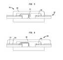
- FIG. 3Ais a sectional view of a microelectronic assembly in accordance with an embodiment.
- FIG. 3Bis a sectional view along a section line transverse to the sectional view of FIG. 3A in the embodiment shown in FIG. 3A .
- FIG. 3Cis a plan view of the embodiment shown in FIGS. 3A-B .
- FIG. 3Dis a diagram graphing characteristic impedance Z 0 relative to separation height H for different diameters of bond wire, in accordance with an embodiment.
- FIG. 4Ais a sectional view illustrating a microelectronic assembly in accordance with a variation of the embodiment illustrated in FIGS. 1A-B .
- FIG. 4Bis a sectional view along a section line transverse to the sectional view of FIG. 4A in the embodiment shown in FIG. 4A .
- FIG. 4Cis a sectional view illustrating a microelectronic assembly in accordance with a variation of the embodiment illustrated in FIGS. 4A-B .
- FIG. 4Dis a sectional view transverse to the sectional view of FIG. 4C , illustrating a microelectronic assembly in accordance with a particular embodiment.
- FIG. 4Eis a sectional view illustrating a microelectronic assembly in accordance with a variation of the embodiment illustrated in FIG. 4C .
- FIG. 4Fis a partial sectional view illustrating a variation of the embodiment illustrated in FIG. 4E .
- FIG. 4Gis a sectional view illustrating a microelectronic assembly in accordance with a variation of the embodiment illustrated in FIG. 4C .
- FIG. 5is a sectional view illustrating a variation of the embodiment illustrated in FIGS. 3A-C .
- FIG. 6is a sectional view illustrating a variation of the embodiment illustrated in FIGS. 3A-C .
- FIG. 7is a sectional view transverse to the sectional illustrated in FIG. 6 , illustrating a variation of the embodiment illustrated in FIGS. 3A-C .
- FIG. 8is a sectional view illustrating a microelectronic assembly in accordance with a variation of the embodiment illustrated in FIGS. 3A-C .
- FIG. 9is a sectional view illustrating a microelectronic assembly in accordance with a variation of the embodiment illustrated in FIGS. 3A-C .
- FIG. 10is a sectional view illustrating a microelectronic assembly in accordance with a variation of the embodiment illustrated in FIGS. 3A-C .
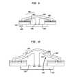
- FIG. 11Ais a sectional view of a microelectronic assembly in accordance with another embodiment.
- FIG. 11Bis a plan view corresponding to the sectional view of FIG. 11A in accordance with one embodiment.
- FIG. 12is a plan view illustrating a microelectronic assembly in accordance with a variation of the embodiment illustrated in FIGS. 11A-B .
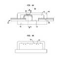
- FIG. 1Ashows a sectional view of an example microelectronic assembly 100 , according to one embodiment.
- FIG. 1Bis a corresponding plan view from above, in which the view in FIG. 1A is through section line 1 A- 1 A of FIG. 1B .
- microelectronic assembly 100includes a microelectronic device 110 conductively connected to interconnection element 130 through a wire bond 165 .
- the microelectronic assembly 100differs from conventional arrangements in that it includes a conductor 166 which is insulatively sheathed by an insulative (dielectric) coating 168 . Beyond the dielectric coating 168 , a conductive encapsulant 160 covers and at least substantially surrounds the wire bond 165 .
- the conductive encapsulant 160is disposed at an at least relatively uniform distance (which can be a uniform distance) from the internal conductor 166 , such that the conductive encapsulant can act as a reference conductor in a transmission line that includes the central conductor 166 and the conductive encapsulant 160 .
- Microelectronic device 110can be a single “bare”, i.e., unpackaged die, e.g., a semiconductor chip having microelectronic circuitry thereon. In alternative embodiments, microelectronic device 110 can include a packaged semiconductor die. Initially, a plurality of contacts 112 are exposed at a surface 128 of the microelectronic device. For example, a plurality of contacts 112 can be exposed at a contact-bearing surface of a semiconductor die and may be arranged in one or more rows exposed at such surface.
- topi.e., contact-bearing surface 128 of a semiconductor chip 110 .
- upwardor “rising from” shall refer to the direction orthogonal and away from the chip top surface 128 .
- Directions referred to as “downward”shall refer to the directions orthogonal to the chip top surface 128 and opposite the upward direction.
- a “vertical” directionshall refer to a direction orthogonal to the chip top surface.
- the term “above” a reference pointshall refer to a point upward of the reference point, and the term “below” a reference point shall refer to a point downward of the reference point.
- top of any individual elementshall refer to the point or points of that element which extend furthest in the upward direction, and the term “bottom” of any element shall refer to the point or points of that element which extend furthest in the downward direction.
- Interconnection element 130is capable of being connected with microelectronic device by electrically conductive interconnections.
- the interconnection elementcan be an element of a package having a plurality of conductive leads or traces 135 , a plurality of first contacts 175 , 180 connected to the leads or traces arranged generally at first locations for interconnection with the microelectronic device, and a plurality of second contacts 175 ′, 180 ′ arranged generally at second locations, for example, for interconnection to another element such as for external interconnection to a printed circuit board.
- the interconnection elementcan be another microelectronic device or a unit including one or more such devices, among others.
- the interconnection element 130may include a solder mask or other dielectric film 150 which can at least partially cover traces 135 , while exposing contacts for forming the conductive interconnections.
- contacts 175 , 175 ′can carry signals, i.e., voltages or currents which vary with time and which typically convey information.
- signalsi.e., voltages or currents which vary with time and which represent state, change, a measurement, a clock or timing input or a control or feedback input are examples of signals.
- contacts 180 , 180 ′can provide connections to ground or a power supply voltage.
- a connection to ground or a power supply voltagetypically provides a reference in a circuit to a voltage which is at least fairly stable with time over frequencies of interest to the operation of the circuit.
- the contacts 175 , 175 ′, 180 , 180 ′Prior to forming conductive interconnections between the microelectronic device and the interconnection element, the contacts 175 , 175 ′, 180 , 180 ′ are exposed at an outwardly-directed face 190 of the interconnection element 130 .
- a statement that an electrically conductive structure is “exposed at” a surface of a dielectric structureindicates that the electrically conductive structure is available for contact with a theoretical point moving in a direction perpendicular to the surface of the dielectric structure toward the surface of the dielectric structure from outside the dielectric structure.
- a terminal or other conductive structure which is exposed at a surface of a dielectric structuremay project from such surface; may be flush with such surface; or may be recessed relative to such surface and exposed through a hole or depression in the dielectric.
- the interconnection elementcan include a “substrate”, e.g., a dielectric element bearing a plurality of traces and contacts.
- a substratecan be a sheet-like flexible dielectric element, typically made of a polymer, e.g., polyimide, among others, having metal traces and contacts patterned thereon, the contacts being exposed at at least one face of the dielectric element.
- the dielectric elementcan have a thickness of 200 micrometers or less in a direction extending away from the surface 128 of the microelectronic device.
- a interconnection element 130 having a dielectric element 120has electrically conductive interconnections with a microelectronic device 110 through wirebonds 165 .
- the wirebondscan be formed using insulated wires.
- a wire-bond using an insulated wirecan have advantages over other types of wire-bonds.
- the insulated wirecan prevent short circuiting if wires should cross and can provide mechanical protection or reinforcement for the wires that might not be available otherwise.
- a process for attaching an insulated wire from a microelectronic device to a interconnection elementwill now described with reference to FIGS. 1A-B .
- the insulative coating 168 of the wire bond 165can have a thickness selected in accordance with a dimension (e.g., a diameter) of the wire 166 .
- the thickness of the insulative coatingcan be determined as the dimension of the coating in an orthogonal direction away from an exterior surface of a central conductive metallic core of the wire.
- the diameter of the central metallic core of the wirecan be about 1 mil (0.001 inch) or less, a measurement equivalent to about 30 micrometers or less (hereinafter, references to micrometers are stated alternatively as “micrometers”, “microns” or “v”).
- the thickness of the insulative coatingcan be selected to have a thickness between about 30 microns and about 75 microns, i.e., between about 1 and 3 mils.
- the wire 166is conductively and mechanically connected to a contact 175 of interconnection element 130 and to a contact 125 , e.g., a bond pad on microelectronic device 110 .
- the device contacts to which insulated wire 165 connectscan be a signal pad or a ground pad of the microelectronic device.
- a wire-bondcan be formed by joining a metal wire typically gold or copper, the wire having an insulating coating, to a contact 112 on the microelectronic device 110 , then drawing the wire and attaching it to a corresponding contact or contact 175 of interconnection element 130 .
- the wiremay be joined to the pad of the subassembly 130 first and joined to the contact of the microelectronic device 110 thereafter.
- a wirebond 165can be formed using a wire having a layer of insulation pre-formed thereon, such wire being provided on a feed spool to an automated wire-bonder.
- the insulative coating as provided on the wire fed to the wire-bondermay have a rather small thickness, for example, a thickness of one to a few microns.
- the insulative coating at the tip of the wirecan be flamed away by the wire-bonder equipment just prior to forming the joint with each contact.
- the insulative coating of the wire-bond 165may be relatively thin when the wire-bond is initially formed on the chip.
- an insulative coating which is available on the bonding wiremay have a thickness of only about one micron to a few microns.
- the thickness of the sheathingmay be such that the sheathing can be easily consumed when a wire-bonding tool applies heat or a flame to an exposed tip of the bonding wire before attaching the tip to a contact of a device or subassembly to form one end of the wire-bond.
- a processcan be applied to the wire-bonds to add a further insulative layer to the insulative coating such that the coating grows to a desirable thickness.
- certain insulative materialscan have an affinity for molecules in a liquid composition, such that when exposed to such liquid composition, molecules can selectively aggregate upon the insulative coating to cause the thickness of the insulative coating to increase.
- the thickness of the insulative coatingcan be at least about 30 microns in order to achieve a desirable separation distance between the insulated wire-bond and a conductive material to be used as a reference conductor therefor.
- the separation distanceis a factor which, along with the cross-sectional dimension, e.g., diameter, of the wire-bond, partly determines the impedance of the wire-bond structure.
- the thickness of the insulative coatingcan be greater, e.g., 50 microns, 75 microns, 100 microns, or another value, depending upon the diameter of the wire 166 , the permeability of the insulative coating and the impedance value to be achieved.
- globs 169 , 179 of dielectric materialcan be deposited to cover any portions of the microelectronic device contacts 112 and the contacts 175 of the interconnection element which may still be exposed.
- the amount of dielectric materialcan be limited to only that which is necessary to ensure that the contacts 112 and contacts 175 are fully insulated for subsequent processing. Therefore, the dielectric material could be relatively thin, i.e., not needing to be more than a few microns in thickness.
- Such insulating dielectric material layercould be deposited, for example, by a spin-on or spray-on process or by filling to a certain height. In one embodiment ( FIG. 2 ), the insulating dielectric material 169 ′, 179 ′ could be deposited onto exposed portions of the contacts 112 and the element contacts 175 to a depth sufficient to insulate the contacts from subsequently deposited conductive material.
- a conductive layer 160can be formed.
- a conductive encapsulantcan be dispensed over insulated wire 165 to form the conductive layer 160 .
- the conductive layer 160can encapsulate the insulated wire 165 in its entirety.
- the conductive materialcan be a conductive paste, e.g., a silver paste, solder paste, or the like. In alternative embodiments, it might be a different material.
- the conductive layer 160forms a conductive interconnection with contacts 180 of the interconnection element when the conductive layer 160 is formed.
- contacts 180 on the interconnection elementcan be exposed at the time the conductive encapsulant is provided on the structure such that the encapsulant then makes electrically conductive contact with the contacts.
- the contact 180is a ground contact
- the conductive encapsulant 160provides a ground reference for transmission lines formed by the juxtaposition of the insulated wirebonds 165 and the ground reference through the conductive layer 160 .
- a transmission line structureis realized for insulated wirebonds 165 which connect with signal contacts on the interconnection element 130 .
- parameters of the structurecan be selected so as to achieve a desired characteristic impedance. For example, in some electronic systems, a characteristic impedance of 50 ohms can be selected in order to meet signal interface requirements, such as when signals on an external interface are transmitted on transmission lines having 50 ohm characteristic impedance.
- parameterscan be selected such as the conductive properties of the metal, as well as the shape and thickness of the wire, the thickness of the dielectric insulating material, its dielectric constant, i.e., permeability, as well as the properties of the conductive layer 160 , e.g., conductive encapsulant.
- the structure described abovemay be performed in the order described, or, alternatively, in a different order. In some implementations, two or more of the described steps may be combined into a single step. In other implementations, a described step may be excluded completely from the process. In yet other variants, additional processing steps may be required.
- at least one second microelectronic devicecould be disposed in the place of interconnection element 130 and be conductively connected to the microelectronic device 110 with insulated wires to achieve transmission line structures in like manner as in the above-described microelectronic assembly 100 .
- the contacts of two interconnection elements 130could be conductively connected with insulated bond wires to achieve transmission line structures in a manner as described above. For example, the contacts of two or more circuit panels or two or more other interconnection components could be interconnected in such manner
- FIG. 3Ashows a sectional view of an exemplary microelectronic assembly 300 that includes a plurality of impedance controlled wire-bonds.
- FIG. 3Cshows a corresponding plan view from above, wherein FIG. 3A is a view through line 3 A- 3 A of FIG. 3C .
- FIG. 3Bis a sectional view through line 3 B- 3 B of FIG. 3C , in a direction transverse to the section that is illustrated in FIG. 3A .
- Microelectronic assembly 300includes microelectronic device 310 and interconnection element 330 .
- Microelectronic device 310in one embodiment, is similar to microelectronic device 110 described in connection with FIGS. 1A-B .
- interconnection element 330is similar to interconnection element 130 described in connection with FIGS. 1A-B .
- a contact 312 at a surface 328 of a microelectronic device 310is wire-bonded to interconnection element 330 using a wire 365 .
- the wire 365typically is not insulated.
- typically a plurality of such wires 365are bonded to microelectronic device 310 and to interconnection element 330 using conventional wire-bonding techniques.
- the wires 365can be different from the insulated wires 165 discussed above.
- wires 365may be typical of the types of wires used in a conventional wire-bonding process.
- wires 365may consist essentially of copper, gold, a gold-silver alloy, or some other metal or alloy of a metal with one or more other metals or materials or an alloy of a metal with one or more other metals and one or more other materials.
- Wirebondscan be formed with relatively precise placement and within desirable tolerances such that parallel, closely spaced runs can be achieved which run parallel to the surface 328 of the die.
- paralleldenotes a structure which is parallel to another structure within manufacturing tolerances.
- wirebonding equipmentavailable from Kulicke and Soffa (hereinafter, “K&S”) can be used to achieve precision wirebonds.
- K&SKulicke and Soffa
- wirebonds 365can be formed which have runs which are perfectly straight in lateral directions above the chip surface or are close to being straight. While such precision can be achieved in forming the wirebonds, nothing is meant to require precisely formed parallel, straight wirebonds other than as specifically recited in the appended claims.
- a dielectric layer 350is formed to cover and insulate the bond wires.
- the dielectric 350in this case might be one of a number of different materials such as a polymer, e.g., an epoxy, or another dielectric material, etc.
- dielectric material 350fills the entire void between interconnection element 330 and microelectronic device 310 .
- the wirebonds 365have runs which extend in directions into and out of the sheet on which FIG. 3B is printed.
- the runs of the wirebondsdefine a plane 377 that extends in directions as shown in FIGS. 3A-B .
- the dielectric materialcan be formed on the interconnection element 330 and microelectronic device 310 by molding so as to produce a molded dielectric region having a surface remote from the microelectronic device surface 328 , and form a surface which is at least substantially planar.
- Such remote surface of the dielectric layercan be spaced at an least a substantially uniform distance “D” in a vertical direction 380 from the plane 377 in which the wirebonds 365 run.
- the molded dielectric regionmay be formed in such manner that its surface which is remote from the microelectronic device surface 328 is parallel to runs of the wirebonds 365 over at least about 50% of the length of the wirebond.
- a conductive layer 360is formed over the dielectric layer 350 .
- the conductive layer 360can be provided by any of a variety of ways.
- the conductive layer 360can extend along and abut the surface of the dielectric layer 350 as shown in FIGS. 3A-B , so as to have a conductive surface 375 in contact with above-described surface of the dielectric layer.
- the conductive layercan be formed by plating, sputtering or otherwise depositing a layer of metal onto a surface of the dielectric layer.
- the conductive layer 360can be formed by a conductive particle-filled thermosetting resin which is vacuum-formed within a forming cavity to a selected shape and distance above the wirebonds 365 .
- the conductive layeris formed by applying a conductive paste, e.g., a silver paste, solder paste, or other conductive filled paste to exposed surfaces of the dielectric layer, such as by a dispensing, molding, screen-printing or stenciling process.
- a conductive pastee.g., a silver paste, solder paste, or other conductive filled paste
- Other examples of conductive pastescan include a conductive polymer or a polymer alloyed with host resins.
- the conductive pastemight comprise an electric conductive powder, an organic binder (e.g. a polyhydroxystyrene derivative) and a thermosetting resin.
- a possible benefit of using a conductive pastecan be obtaining a finished product that may be lighter in weight. Fabrication might also be easier and less expensive if it can result in the elimination of secondary processes.
- conductive layer 360contacts a pad 370 on interconnection element 330 .
- the padmight be a ground or power-supply pad.
- dimensions of the conductive layer 360 in directions oriented horizontally with respect to the surface 328 of microelectronic device 310can be smaller than corresponding dimensions of the microelectronic device surface 328 .
- the surface 328 of the microelectronic devicehas a first dimension 324 extending in a first direction and has a second dimension 334 extending in a second direction that is transverse to the first direction.
- the first and second directionsextend horizontally with respect to the microelectronic device surface 328 , that is, in directions along such surface.
- the conductive layer 360can have a dimension 326 in the first direction which is smaller than the corresponding first dimension 324 of the microelectronic device surface 328 .
- the conductive layer 360can have a dimension 336 in the second direction which is smaller than the corresponding second dimension 334 of the microelectronic device surface 328 .
- the conductive layer 360can have a surface 375 which is disposed at at least a substantially uniform distance above at least substantial portions of the lengths of the wirebonds, such that each wirebond and the adjacent conductive layer, being tied to a source of reference voltage, forms a transmission line structure that has a desired characteristic impedance.
- the conductive surfacecan be disposed at such substantially uniform distance from runs of the wirebonds which extend over 50% or more of the lengths of the wirebonds.
- parameterscan be selected such as the conductive properties of the metal used in the wire, as well as the shape and thickness of the wire, the thickness of the insulating material 350 between the wire and the conductive layer 360 , the dielectric constant of the insulating material, i.e., permeability, as well as the thickness and properties of the conductive layer 360 .
- FIG. 3Dgraphs characteristic impedance Z 0 , in ohms, versus separation distance, in inches, between a signal conductor or conductive element, e.g., a wire of cylindrical cross-section, and a reference conductor or conductive element, e.g., “ground plane”.
- the reference conductoris assumed to be a planar structure that is large in comparison with the diameter of the signal conductor.
- FIG. 3Dplots characteristic impedance for two different diameter wires.
- the plots in FIG. 3Dcan be derived from an equation that governs characteristic impedance in an arrangement having the present geometry. In such equation, the characteristic impedance Z 0 is given by
- Z 0138 ⁇ log ⁇ ⁇ ( 4 ⁇ ⁇ H / d ) ⁇ R ⁇ ⁇ ohms , where H is the separation distance between the wire and the conductive plane, d is the diameter of the wire and ⁇ R is the permeability of the dielectric material that separates the wire from the conductive plane.
- the permeability ⁇ Rcan vary depending on the type of dielectric material used.
- the separation distance His a factor which can be at least partly determined by the process used to fabricate the microelectronic assembly.
- the wire diametermay be at least partly determined by the process used to fabricate the microelectronic assembly.
- the lower curve 320plots the characteristic impedance when the wire used to form a wirebond has a thickness of 1 mil, i.e., 0.001 inch.
- the upper curveplots 322 the characteristic impedance when the wire used to form the wirebond has a thickness of 0.7 mil, i.e., 0.0007 inch.
- characteristic impedances lower than about 70 ohmsare provided when a separation distance H between the wire and the conductive plane is less than or equal to about 0.002 inch (2 mils), i.e., about 50 microns.
- FIG. 3Bshows a cross section of microelectronic assembly 300 .
- This figureshows that multiple bondwires can be bonded from the interconnection element 330 to the microelectronic device 310 and that each of the thus formed wirebonds in the assembly 300 is surrounded by dielectric material 350 .
- the conductive encapsulantas illustrated, can cover the entire subassembly. In an alternative embodiment, the conductive encapsulant may only cover a portion of the dielectric material 350 , such as a top surface of the dielectric material 350 .
- FIGS. 4A-4Bshow an alternative assembly 400 which represents a variation from the assembly 300 shown in FIG. 3 .
- FIG. 4Ais an elevational view and FIG. 4B is a corresponding sectional in a direction transverse to the view illustrated in FIG. 4A .
- two wires 465 and 466are wire-bonded between respective pairs of contacts of the interconnection element 430 and the microelectronic device 410 .
- wire 465is a signal wire (e.g. used to transfer signals between interconnection element 430 and microelectronic device 410 ) and the other wire 466 is a ground or power wire, i.e., a wire that is bonded to a ground or power contact of the interconnection element 430 .
- a reference wirebond 466is formed such that it extends to a higher location above the contact-bearing surface 428 of microelectronic device 410 than wire 465 . Accordingly, when dielectric material 450 is provided over wires 465 and 466 , wire 466 is not completely covered by the dielectric material 450 . Consequently, the wire 466 remains at least partially exposed when the conductive layer 460 is formed. Then, when the conductive layer 460 is formed, the layer 460 contacts the wire 466 and forms an electrically conductive connection with the wire.
- the wire 466may be connected to respective reference contacts (e.g., ground contacts or voltage supply contacts) on the microelectronic device and the interconnection element. As further seen in FIG.
- the conductive layeris connected to a reference contact 480 (e.g., a ground or power contact pad) of the interconnection element.
- the conductive layercan act as a reference conductor for a transmission line that includes the signal wire 465 and the reference wire 466 and may also include the conductive layer 460 as a part of the transmission line.
- the reference wire 466is also connected to a contact on the microelectronic device 410 , the transmission line formed by the signal and reference wires 465 , 466 extends to the contacts on the microelectronic device.
- FIG. 4Cis a sectional view illustrating a variation of the embodiment shown in FIGS. 4A-B .
- the reference wire 476extends to a higher location above the surface 428 of the microelectronic device than a signal wire 475 .
- the conductive layer 462like the conductive layer 460 of FIGS. 4A-B , presents an at least generally planar surface 464 in contact with the insulating dielectric layer 450 .
- the conductive layer 462additionally has a contacting portion 478 which extends downwardly away from surface 464 towards the microelectronic device 410 .
- Such contacting portion 478has an electrically conductive connection with the reference wire 466 but is insulated from the signal wire 475 .
- the conductive layer 462 with contacting portion 478 as shown in FIG. 4Ccan be formed as follows.
- the signal wire and reference wireare formed and a dielectric encapsulant layer 450 can be formed thereon, which has at least sufficient hardness to resist flowing in subsequent processing.
- a trenchis formed extending downward from an outer surface of the dielectric encapsulant material which exposes the reference wire 476 .
- a mechanical or laser processcan be used to remove material from the encapsulant layer.
- the conductive materialextends downward into the trench and forms an electrically conductive connection between the conductive layer 462 and the reference wire 466 .
- FIG. 4Dillustrates a variation of the embodiment described with respect to FIG. 4C .
- FIG. 4Dis a transverse sectional view that is taken in a direction that corresponds to direction line 4 D- 4 D of FIG. 4C , such that the signal wires 485 and the reference wires 486 appear to run in directions into and out of the plane of the sheet on which FIG. 4D is printed.
- the runs of the reference wires 486lie substantially in the same plane as the runs of the signal wires 485 .
- the contacting portions 488are disposed in trenches which extend downwardly towards the microelectronic device 410 from the at least generally planar surface 464 of the conductive layer such that the reference wires are disposed in contact with the conductive material of the contacting portions, while the signal wires 485 are disposed in contact with the dielectric encapsulating material 450 .
- FIG. 4Eillustrates a variation of the embodiment ( FIG. 4D ) in which the reference wire 496 and the signal wire 495 have runs which are disposed at least substantially within the same plane above the surface 428 of the microelectronic device 410 , but in which a reference wire 496 extends in a direction opposite a direction 495 in which the signal wire extends.
- the contact between the reference wire 496 and the conductive layer 460can be used to establish a stable reference voltage along the length of the reference wire 496 and on the surface 464 of the conductive layer. Consequently, the reference wire 496 acts as a reference conductor for the signal wire for the portion 491 of the signal wire 495 that extends in an upward direction from the microelectronic device 410 .
- the conductive layer 460acts as the reference conductor for the other portion of the signal wire that extends in a direction along the surface 428 of the microelectronic device and at least generally to the surface 464 of the conductive layer 460 .
- the reference wire 496 ′can include an upwardly extending portion 497 or “kinked” portion, rather than just extending in a direction generally parallel to the surface 428 of the microelectronic device 410 .
- Such shapecan help assure that a good electrically conductive connection is established between the reference wire 496 ′ and the connecting portion 498 of the conductive layer.
- the reference wire 508has electrically conductive connections at each end to the substrate or interconnection element. Other features of this variation are as described above with reference to one or more of FIGS. 4A-F .
- FIG. 5illustrates an alternative embodiment of a microelectronic assembly 300 .
- microelectronic assembly 500includes microelectronic device 510 and interconnection element 530 .
- the dielectric material 550includes a groove 570 .
- This groovecan be molded into the assembly as the dielectric layer 550 is formed.
- groove 570is cut after the dielectric has cured. Groove 570 could be cut via drilling, sawing, or some other technique.
- the conductive layer 560when the conductive layer 560 is formed, the conductive layer extends into groove 570 .
- the conductive layermay then include conductive material within the groove disposed adjacent to rising portions of wirebonds, that is, adjacent to portions of a plurality of wirebonds which rise in a vertical direction away from the microelectronic device surface, as shown in FIG. 5 .
- FIG. 6illustrates another alternative embodiment of interconnection element 300 .
- conductive layer 660is extended to overlie the traces 635 on interconnection element 630 , as insulated therefrom by dielectric layer 670 , e.g., a patterned dielectric layer such as solder mask. Doing so extends the impedance control and shielding to the traces.
- FIG. 7illustrates a microelectronic assembly 700 according to yet another alternative embodiment.
- the dielectric layer 750includes slots or grooves 770 extending downwardly from a top surface thereof.
- the groovescan extend in a direction parallel to the runs of the wirebonds 765 , i.e., in directions into and out of the plane defined by the page on which FIG. 7 is printed.
- the groovescan be formed, for example, at the time the dielectric layer is formed, e.g., such as, for example, when dielectric material is dispensed. Alternatively, the grooves can be formed after the dielectric material has been dispensed or cured.
- the conductive layer 760When the conductive layer 760 is formed, it can extend into grooves 770 and can provide shielding between wires.
- FIG. 8illustrates a microelectronic assembly 800 according to another alternative embodiment.
- microelectronic device 810is wire-bonded in a face-up orientation with interconnection element 830 .
- a rear face of the microelectronic deviceis attached to the interconnection element, and wirebonds extend from contacts 815 on the microelectronic device to corresponding contacts 875 of the interconnection element, the subassembly contacts 875 being disposed beyond edges 812 of the microelectronic device.
- a stack of microelectronic devices 810can be stacked one on top of the other. Wire bonds can be formed between a microelectronic device 810 and a corresponding interconnection element 830 . Then, a dielectric layer 850 can be formed, and then a conductive layer 860 can be formed. Such layers can be formed so as to leave stack interconnection terminals such as for example, stack contacts (not shown) exposed on the interconnection element 830 . Then, a second completed microelectronic assembly 800 can be stacked on top of the second dielectric layer, e.g., so that the microelectronic devices in each assembly 800 is in a face-up orientation. The second microelectronic assembly can be conductively interconnected with the first microelectronic assembly with conductive elements extending between the stack interconnection terminals.
- FIG. 9illustrates a variation of the above embodiment ( FIGS. 3A-B ) in which signal wires 1065 extend in runs along the surface 1028 of the microelectronic device 1010 , where the runs 1067 are not parallel to the plane of the surface 1028 . Instead, the runs 1067 of the wire bonds are canted at an angle relative to the surface 1028 .
- the conductive layer 1060can extend parallel to the runs 1067 at a spacing 1061 which is uniform or at least substantially uniform along 50% or more of the length of the wire bonds. In this way, a transmission line structure is achieved which has a beneficial characteristic impedance.
- the fabrication methodcan be the same as described with respect to FIGS. 3A-B above, except that a mold having a gabled shape can be used to mold the dielectric encapsulant layer 1050 prior to forming the conductive layer.
- FIG. 10illustrates yet another variation in which the wire bonds 1085 do not extend in uniformly linear runs. Instead, the wire bonds have a stair-step shape that includes relatively short jogs 1082 which extend mostly downwardly and somewhat longer jogs or steps 1084 which extend in directions across the surface 1028 of the microelectronic device 1010 .
- the conductive layercan be arranged to have a stair-step shaped inner surface adjacent to the wirebonds 1084 , such inner surface being defined by a series of similar steps which follow the contours of the wirebonds.
- the inner surface of the conductive layer 1080can extend parallel to the jogs 1084 of the wirebonds at a spacing 1081 which is uniform or at least substantially uniform along 50% or more of the length of the wire bonds.
- the same method as described aboveFIGS. 3A-B ) can be used to fabricate the structure except that a mold having a different shape can be used to form the stair-step shaped conductive layer.
- a conductive plane 960extends along a surface 928 of a microelectronic device 910 and wirebonds 965 connected to contacts 912 of the microelectronic device extend parallel to the surface 928 at a spaced distance from the conductive plane 960 .
- FIG. 11Ais a sectional view illustrating a microelectronic assembly 900 including microelectronic device 910 and interconnection element connected therewith.
- FIG. 11Bis a plan view from above the surface 928 and looking towards the surface towards contacts 912 .
- the conductive planecan include openings 964 which expose individual ones of the contacts 912 .
- the conductive planecan include one or more larger openings which expose some or all of the contacts of the microelectronic device.
- the conductive planecan be formed by processing applied to the surface 928 of a microelectronic device such as a metal deposition or plating process applied to the device while the device is in form of a wafer or panel containing a plurality of connected devices or after the device has been singulated from other such devices.
- the conductive planecan be provided by pre-processing a metal sheet such as a copper foil, for example, to form openings 964 in the metal sheet. Then, the metal sheet can be bonded to the surface 928 of the microelectronic device, such as by using an adhesive.
- Wirebonds 965are then formed which connect the contacts 912 of the microelectronic device with the contacts 975 on the microelectronic device 910 .
- the wirebonds 965have runs which are raised above the surface 928 of the microelectronic device.
- a dielectric layer 950can be formed, such as for the purpose of mechanically supporting the wirebonds.
- the runs of the wirebonds 965can extend in a horizontal direction parallel to or at least generally parallel to the microelectronic device surface 928 as shown in FIG. 11A . In this case, the runs may be parallel within manufacturing tolerances therefor.
- Such horizontal runstypically are substantial portions of the wirebonds, i.e., 50% of the lengths of the wirebonds or greater.
- the runscan be spaced at a substantially uniform height above the conductive plane, e.g., typically a height of about 50 micrometers from the surface 928 to about 100 micrometers from the surface 928 .
- a desired impedancecan be achieved for the wirebonds.
- signals to and from the microelectronic devicemay be transmitted with less noise entering the connections (e.g., wirebonds) carrying the signals.
- the conductive layercan be provided in form of a plurality of conductive strips 980 which extend along the surface of the microelectronic device 910 in directions parallel to runs of the signal wire bonds 965 between the device contacts 912 and the contacts 975 of the interconnection element 930 .
- the conductive stripscan be mechanically supported or held together with supporting portions 982 .
- the conductive strips and supporting portionsare formed as a metallic structure by subtractively patterning a copper foil or sheet and bonding the remaining metallic structure to the surface 928 of the microelectronic device, such as with an adhesive material 962 .
- the conductive materialneed not conform to the contours of the dielectric region which surrounds the wirebonds.
- the conductive layercan be realized by attaching a metal can to overlie the bond wires and dielectric region 350 so as to place the interior surface of the metal can at a desired spacing from the wirebonds 365 of the microelectronic assembly.
Landscapes
- Engineering & Computer Science (AREA)
- Microelectronics & Electronic Packaging (AREA)
- Power Engineering (AREA)
- Computer Hardware Design (AREA)
- Physics & Mathematics (AREA)
- General Physics & Mathematics (AREA)
- Condensed Matter Physics & Semiconductors (AREA)
- Health & Medical Sciences (AREA)
- Electromagnetism (AREA)
- Toxicology (AREA)
- Wire Bonding (AREA)
- Internal Circuitry In Semiconductor Integrated Circuit Devices (AREA)
- Measuring Leads Or Probes (AREA)
Abstract
Description
where H is the separation distance between the wire and the conductive plane, d is the diameter of the wire and ∈Ris the permeability of the dielectric material that separates the wire from the conductive plane. The permeability ∈Rcan vary depending on the type of dielectric material used. The separation distance H is a factor which can be at least partly determined by the process used to fabricate the microelectronic assembly. The wire diameter may be at least partly determined by the process used to fabricate the microelectronic assembly.
Claims (12)
Priority Applications (1)
| Application Number | Priority Date | Filing Date | Title |
|---|---|---|---|
| US14/071,055US8994195B2 (en) | 2009-03-13 | 2013-11-04 | Microelectronic assembly with impedance controlled wirebond and conductive reference element |
Applications Claiming Priority (6)
| Application Number | Priority Date | Filing Date | Title |
|---|---|---|---|
| US21006309P | 2009-03-13 | 2009-03-13 | |
| KR1020090089470AKR100950511B1 (en) | 2009-09-22 | 2009-09-22 | Microelectronic assembly with impedance controlled wirebond and conductive reference element |
| KR10-2009-0089470 | 2009-09-22 | ||
| US12/722,784US7923851B2 (en) | 2009-03-13 | 2010-03-12 | Microelectronic assembly with impedance controlled wirebond and conductive reference element |
| US12/986,556US8575766B2 (en) | 2009-03-13 | 2011-01-07 | Microelectronic assembly with impedance controlled wirebond and conductive reference element |
| US14/071,055US8994195B2 (en) | 2009-03-13 | 2013-11-04 | Microelectronic assembly with impedance controlled wirebond and conductive reference element |
Related Parent Applications (1)
| Application Number | Title | Priority Date | Filing Date |
|---|---|---|---|
| US12/986,556ContinuationUS8575766B2 (en) | 2009-03-13 | 2011-01-07 | Microelectronic assembly with impedance controlled wirebond and conductive reference element |
Publications (2)
| Publication Number | Publication Date |
|---|---|
| US20140103500A1 US20140103500A1 (en) | 2014-04-17 |
| US8994195B2true US8994195B2 (en) | 2015-03-31 |
Family
ID=42183995
Family Applications (4)
| Application Number | Title | Priority Date | Filing Date |
|---|---|---|---|
| US12/722,784ActiveUS7923851B2 (en) | 2009-03-13 | 2010-03-12 | Microelectronic assembly with impedance controlled wirebond and conductive reference element |
| US12/986,601ActiveUS8269357B2 (en) | 2009-03-13 | 2011-01-07 | Microelectronic assembly with impedance controlled wirebond and conductive reference element |
| US12/986,556Expired - Fee RelatedUS8575766B2 (en) | 2009-03-13 | 2011-01-07 | Microelectronic assembly with impedance controlled wirebond and conductive reference element |
| US14/071,055ActiveUS8994195B2 (en) | 2009-03-13 | 2013-11-04 | Microelectronic assembly with impedance controlled wirebond and conductive reference element |
Family Applications Before (3)
| Application Number | Title | Priority Date | Filing Date |
|---|---|---|---|
| US12/722,784ActiveUS7923851B2 (en) | 2009-03-13 | 2010-03-12 | Microelectronic assembly with impedance controlled wirebond and conductive reference element |
| US12/986,601ActiveUS8269357B2 (en) | 2009-03-13 | 2011-01-07 | Microelectronic assembly with impedance controlled wirebond and conductive reference element |
| US12/986,556Expired - Fee RelatedUS8575766B2 (en) | 2009-03-13 | 2011-01-07 | Microelectronic assembly with impedance controlled wirebond and conductive reference element |
Country Status (7)
| Country | Link |
|---|---|
| US (4) | US7923851B2 (en) |
| EP (1) | EP2406823A2 (en) |
| JP (1) | JP5651608B2 (en) |
| KR (1) | KR100950511B1 (en) |
| CN (1) | CN102449760A (en) |
| TW (1) | TWI431748B (en) |
| WO (1) | WO2010105157A2 (en) |
Families Citing this family (18)
| Publication number | Priority date | Publication date | Assignee | Title |
|---|---|---|---|---|
| KR100950511B1 (en) | 2009-09-22 | 2010-03-30 | 테세라 리써치 엘엘씨 | Microelectronic assembly with impedance controlled wirebond and conductive reference element |
| KR100935854B1 (en)* | 2009-09-22 | 2010-01-08 | 테세라 리써치 엘엘씨 | Microelectronic assembly with impedance controlled wirebond and reference wirebond |
| US8853708B2 (en) | 2010-09-16 | 2014-10-07 | Tessera, Inc. | Stacked multi-die packages with impedance control |
| US8222725B2 (en) | 2010-09-16 | 2012-07-17 | Tessera, Inc. | Metal can impedance control structure |
| US9136197B2 (en) | 2010-09-16 | 2015-09-15 | Tessera, Inc. | Impedence controlled packages with metal sheet or 2-layer RDL |
| US8581377B2 (en) | 2010-09-16 | 2013-11-12 | Tessera, Inc. | TSOP with impedance control |
| US8786083B2 (en) | 2010-09-16 | 2014-07-22 | Tessera, Inc. | Impedance controlled packages with metal sheet or 2-layer RDL |
| US9123713B2 (en) | 2010-11-24 | 2015-09-01 | Tessera, Inc. | Lead structures with vertical offsets |
| KR101118711B1 (en) | 2010-12-17 | 2012-03-12 | 테세라, 인코포레이티드 | Enhanced stacked microelectric assemblies with central contacts |
| KR101061531B1 (en)* | 2010-12-17 | 2011-09-01 | 테세라 리써치 엘엘씨 | Enhanced stacked microelectronic assemblies with central contacts and improved ground or power distribution |
| FR2980101A1 (en) | 2011-09-20 | 2013-03-22 | Tornier Inc | REINFORCING STRIP FOR THE RESTORATION OF A SOFT TISSUE |
| US9548599B2 (en)* | 2013-08-27 | 2017-01-17 | Labinal, Llc | Thermally managed load module with embedded conductors |
| KR20190057136A (en)* | 2016-10-04 | 2019-05-27 | 더 차레스 스타크 드레이퍼 래보레이토리, 인코포레이티드 | Wiring system |
| FR3058261A1 (en)* | 2016-11-03 | 2018-05-04 | Stmicroelectronics (Grenoble 2) Sas | METHOD FOR MAKING AN ELECTRICAL CONNECTION BETWEEN AN ELECTRONIC CHIP AND A SUPPORT PLATE AND ELECTRONIC DEVICE |
| FR3058259A1 (en)* | 2016-11-03 | 2018-05-04 | Stmicroelectronics (Grenoble 2) Sas | METHOD FOR MAKING AN ELECTRICAL CONNECTION BETWEEN AN ELECTRONIC CHIP AND A SUPPORT PLATE AND ELECTRONIC DEVICE |
| US10224306B2 (en) | 2016-11-03 | 2019-03-05 | Stmicroelectronics (Grenoble 2) Sas | Method for forming an electrical connection between an electronic chip and a carrier substrate and electronic device |
| TWI780576B (en)* | 2020-12-28 | 2022-10-11 | 抱樸科技股份有限公司 | Semiconductor device with cladding wire and method of making the same |
| JP2024038575A (en)* | 2022-09-08 | 2024-03-21 | 三菱電機株式会社 | Semiconductor device, semiconductor device manufacturing method, and power conversion device |
Citations (87)
| Publication number | Priority date | Publication date | Assignee | Title |
|---|---|---|---|---|
| US4680613A (en) | 1983-12-01 | 1987-07-14 | Fairchild Semiconductor Corporation | Low impedance package for integrated circuit die |
| US4980753A (en) | 1988-11-21 | 1990-12-25 | Honeywell Inc. | Low-cost high-performance semiconductor chip package |
| US5028983A (en) | 1988-10-28 | 1991-07-02 | International Business Machines Corporation | Multilevel integrated circuit packaging structures |
| US5065282A (en) | 1986-10-17 | 1991-11-12 | Polonio John D | Interconnection mechanisms for electronic components |
| US5343074A (en) | 1993-10-04 | 1994-08-30 | Motorola, Inc. | Semiconductor device having voltage distribution ring(s) and method for making the same |
| JPH06268100A (en) | 1993-03-12 | 1994-09-22 | Nippon Telegr & Teleph Corp <Ntt> | Semiconductor device sealing structure and sealing method |
| US5394010A (en) | 1991-03-13 | 1995-02-28 | Kabushiki Kaisha Toshiba | Semiconductor assembly having laminated semiconductor devices |
| JPH0758138A (en) | 1993-08-16 | 1995-03-03 | Nec Corp | Structure and method for wire bonding |
| US5468999A (en) | 1994-05-26 | 1995-11-21 | Motorola, Inc. | Liquid encapsulated ball grid array semiconductor device with fine pitch wire bonding |
| US5471151A (en) | 1990-02-14 | 1995-11-28 | Particle Interconnect, Inc. | Electrical interconnect using particle enhanced joining of metal surfaces |
| US5523621A (en) | 1994-05-15 | 1996-06-04 | Kabushiki Kaisha Toshiba | Semiconductor device having a multilayer ceramic wiring substrate |
| US5552631A (en) | 1992-06-04 | 1996-09-03 | Lsi Logic Corporation | Semiconductor device assembly including power or ground plane which is provided on opposite surface of insulating layer from signal traces, and is exposed to central opening in insulating layer for interconnection to semiconductor die |
| JPH0927512A (en) | 1995-07-10 | 1997-01-28 | Mitsubishi Electric Corp | Semiconductor device |
| US5606196A (en) | 1995-10-14 | 1997-02-25 | Samsung Electronics Co., Ltd. | High-frequency, high-density semiconductor chip package with screening bonding wires |
| US5639989A (en) | 1994-04-19 | 1997-06-17 | Motorola Inc. | Shielded electronic component assembly and method for making the same |
| US5835988A (en) | 1996-03-27 | 1998-11-10 | Mitsubishi Denki Kabushiki Kaisha | Packed semiconductor device with wrap around external leads |
| US5880403A (en) | 1994-04-01 | 1999-03-09 | Space Electronics, Inc. | Radiation shielding of three dimensional multi-chip modules |
| EP0915504A1 (en) | 1994-04-28 | 1999-05-12 | Fujitsu Limited | Semiconductor package and method of forming the same |
| US6001671A (en) | 1996-04-18 | 1999-12-14 | Tessera, Inc. | Methods for manufacturing a semiconductor package having a sacrificial layer |
| JP2000021926A (en) | 1998-07-06 | 2000-01-21 | Hitachi Ltd | Semiconductor device |
| KR100270817B1 (en) | 1997-05-22 | 2000-11-01 | 이해영 | Package for high speed and high frequency device |
| JP2000332160A (en) | 1999-05-24 | 2000-11-30 | Sumitomo Metal Electronics Devices Inc | Cavity down type semiconductor package |
| JP2001007140A (en) | 1999-04-23 | 2001-01-12 | Sharp Corp | High frequency semiconductor device |
| US6326678B1 (en) | 1993-09-03 | 2001-12-04 | Asat, Limited | Molded plastic package with heat sink and enhanced electrical performance |
| JP2001339016A (en) | 2000-05-30 | 2001-12-07 | Alps Electric Co Ltd | Surface mounting electronic circuit unit |
| US6445594B1 (en) | 2000-02-10 | 2002-09-03 | Mitsubishi Denki Kabushiki Kaisha | Semiconductor device having stacked semiconductor elements |
| US6476506B1 (en) | 2001-09-28 | 2002-11-05 | Motorola, Inc. | Packaged semiconductor with multiple rows of bond pads and method therefor |
| US6518659B1 (en) | 2000-05-08 | 2003-02-11 | Amkor Technology, Inc. | Stackable package having a cavity and a lid for an electronic device |
| US6538336B1 (en) | 2000-11-14 | 2003-03-25 | Rambus Inc. | Wirebond assembly for high-speed integrated circuits |
| US6552417B2 (en) | 1993-09-03 | 2003-04-22 | Asat, Limited | Molded plastic package with heat sink and enhanced electrical performance |
| US20030090001A1 (en) | 2001-11-13 | 2003-05-15 | Kulicke And Soffa Investments, Inc. | Wirebonded semiconductor package structure and method of manufacture |
| US6667546B2 (en) | 2001-11-15 | 2003-12-23 | Siliconware Precision Industries Co., Ltd. | Ball grid array semiconductor package and substrate without power ring or ground ring |
| JP2004112143A (en) | 2002-09-17 | 2004-04-08 | Sumitomo Metal Electronics Devices Inc | Connecting structure of conductor for high frequency signal and semiconductor integrated circuit package |
| US6770822B2 (en) | 2002-02-22 | 2004-08-03 | Bridgewave Communications, Inc. | High frequency device packages and methods |
| US20040164389A1 (en) | 2003-02-25 | 2004-08-26 | I Tseng Lee | [chip package and process for forming the same] |
| US6812580B1 (en)* | 2003-06-09 | 2004-11-02 | Freescale Semiconductor, Inc. | Semiconductor package having optimized wire bond positioning |
| US20040238939A1 (en) | 2001-01-04 | 2004-12-02 | Ping Wu | Multi-power ring chip scale package for system level integration |
| KR20050002659A (en) | 2003-06-30 | 2005-01-10 | 엔이씨 가꼬오부쯔 디바이스 가부시끼가이샤 | Hybrid integrated circuit |
| US20050006742A1 (en) | 2002-08-21 | 2005-01-13 | Kabushiki Kaisha Toshiba | High frequency semiconductor module, high frequency semiconductor device and manufacturing method for the same |
| WO2005010989A1 (en) | 2003-07-30 | 2005-02-03 | Koninklijke Philips Electronics, N.V. | Ground arch for wirebond ball grid arrays |
| US20050045378A1 (en) | 2003-08-29 | 2005-03-03 | Heng Mung Suan | Stacked microfeature devices and associated methods |
| US20050098870A1 (en) | 2003-08-27 | 2005-05-12 | Jochen Thomas | FBGA arrangement |
| US20050116013A1 (en) | 2003-11-28 | 2005-06-02 | International Business Machines Corporation | Method and structure for controlled impedance wire bonds using co-dispensing of dielectric spacers |
| US20060049505A1 (en) | 2002-12-10 | 2006-03-09 | Koninklijke Philips Electronics N.V. | High density interconnect power and ground strap and method therefor |
| US20060125079A1 (en) | 2002-12-10 | 2006-06-15 | Chris Wyland | High density package interconnect wire bond strip line and method therefor |
| US20060131742A1 (en) | 2004-12-16 | 2006-06-22 | Fine Tech. Inc. | Packaged chip capable of lowering characteristic impedance |
| US20060145308A1 (en) | 2005-01-05 | 2006-07-06 | International Business Machines Corporation | On-chip circuit pad structure |
| US20060175712A1 (en) | 2005-02-10 | 2006-08-10 | Microbonds, Inc. | High performance IC package and method |
| JP2006216823A (en) | 2005-02-04 | 2006-08-17 | Akita Denshi Systems:Kk | Semiconductor device, its manufacturing method and electronic device |
| US20070007644A1 (en) | 2000-12-22 | 2007-01-11 | Broadcom Corporation | Ball grid array package enhanced with a thermal and electrical connector |
| US7166495B2 (en) | 1996-02-20 | 2007-01-23 | Micron Technology, Inc. | Method of fabricating a multi-die semiconductor package assembly |
| US20070034674A1 (en) | 2003-06-27 | 2007-02-15 | Kabushiki Kaisha Shinkawa | Semiconductor device |
| KR100702970B1 (en) | 2005-07-06 | 2007-04-03 | 삼성전자주식회사 | Semiconductor package having binary connection method and manufacturing method thereof |
| EP1770777A2 (en) | 1998-07-06 | 2007-04-04 | Hitachi, Ltd. | Semiconductor device |
| US7205651B2 (en) | 2004-04-16 | 2007-04-17 | St Assembly Test Services Ltd. | Thermally enhanced stacked die package and fabrication method |
| US20070105272A1 (en) | 2005-08-24 | 2007-05-10 | Micron Technology, Inc. | Microelectronic devices and microelectronic support devices, and associated assemblies and methods |
| US20070170601A1 (en) | 2003-12-26 | 2007-07-26 | Yoshinori Miyaki | Semiconductor device and manufacturing method of them |
| WO2008008948A2 (en) | 2006-07-14 | 2008-01-17 | Texas Instruments Incorporated | System and method of attenuating electromagnetic interference with a grounded top film |
| US20080088012A1 (en) | 2006-08-15 | 2008-04-17 | Yamaha Corporation | Semiconductor device and wire bonding method therefor |
| US20080111248A1 (en) | 2004-12-14 | 2008-05-15 | Chee Seng Foong | Flip Chip And Wire Bond Semiconductor Package |
| US7450110B2 (en) | 2000-01-19 | 2008-11-11 | Immersion Corporation | Haptic input devices |
| US7456505B2 (en) | 2005-07-29 | 2008-11-25 | Infineon Technologies Ag | Integrated circuit chip and integrated device |
| US7466021B2 (en) | 2003-11-17 | 2008-12-16 | Interconnect Portfolio, Llp | Memory packages having stair step interconnection layers |
| US7468560B2 (en) | 2005-01-19 | 2008-12-23 | Infineon Technologies Ag | Semiconductor device with micro connecting elements and method for producing the same |
| CN101410974A (en) | 2006-03-23 | 2009-04-15 | Nxp股份有限公司 | Enhanced electronic bond wire package |
| US7528011B2 (en) | 1999-02-17 | 2009-05-05 | Sharp Kabushiki Kaisha | Semiconductor device and manufacturing method thereof |
| US7537962B2 (en) | 2006-12-22 | 2009-05-26 | Stats Chippac Ltd. | Method of fabricating a shielded stacked integrated circuit package system |
| US20090256266A1 (en) | 2008-04-10 | 2009-10-15 | Sierra Monolithics, Inc. | Apparatus and method for a chip assembly including a frequency extending device |
| KR100935854B1 (en) | 2009-09-22 | 2010-01-08 | 테세라 리써치 엘엘씨 | Microelectronic assembly with impedance controlled wirebond and reference wirebond |
| WO2010020836A1 (en) | 2008-08-22 | 2010-02-25 | Taiwan Semiconductor Manufacturing Co., Ltd | Impedance controlled electrical interconnection employing meta-materials |
| KR100950511B1 (en) | 2009-09-22 | 2010-03-30 | 테세라 리써치 엘엘씨 | Microelectronic assembly with impedance controlled wirebond and conductive reference element |
| US7723852B1 (en) | 2008-01-21 | 2010-05-25 | Amkor Technology, Inc. | Stacked semiconductor package and method of making same |
| US7727801B2 (en) | 2004-08-27 | 2010-06-01 | Texas Instruments Incorporated | Apparatus for improved power distribution in wirebond semiconductor packages |
| US7768135B1 (en) | 2008-04-17 | 2010-08-03 | Amkor Technology, Inc. | Semiconductor package with fast power-up cycle and method of making same |
| US20100270667A1 (en) | 2009-04-24 | 2010-10-28 | Infineon Technologies Ag | Semiconductor package with multiple chips and substrate in metal cap |
| US7843021B2 (en) | 2008-02-28 | 2010-11-30 | Shandong Gettop Acoustic Co. Ltd. | Double-side mountable MEMS package |
| US7855463B2 (en) | 2006-09-12 | 2010-12-21 | Qimonda Ag | Method for producing a circuit module comprising at least one integrated circuit |
| US7875985B2 (en) | 2006-12-22 | 2011-01-25 | Qimonda Ag | Memory device |
| US8026129B2 (en) | 2006-03-10 | 2011-09-27 | Stats Chippac Ltd. | Stacked integrated circuits package system with passive components |
| US20120068338A1 (en) | 2010-09-16 | 2012-03-22 | Tessera Research Llc | Impedance controlled packages with metal sheet or 2-layer rdl |
| US20120068317A1 (en) | 2010-09-16 | 2012-03-22 | Tessera Research Llc | Tsop with impedance control |
| US20120068361A1 (en) | 2010-09-16 | 2012-03-22 | Tessera Research Llc | Stacked multi-die packages with impedance control |
| US8222725B2 (en) | 2010-09-16 | 2012-07-17 | Tessera, Inc. | Metal can impedance control structure |
| US8237250B2 (en) | 2008-08-21 | 2012-08-07 | Advanced Semiconductor Engineering, Inc. | Advanced quad flat non-leaded package structure and manufacturing method thereof |
| US8243465B2 (en) | 2009-02-18 | 2012-08-14 | Elpida Memory, Inc. | Semiconductor device with additional power supply paths |
| US8253258B2 (en) | 2009-03-30 | 2012-08-28 | Elpida Memory, Inc. | Semiconductor device with hollow and throughhole and method of manufacturing same |
| US8294249B2 (en) | 2008-08-05 | 2012-10-23 | Integrated Device Technology Inc. | Lead frame package |
Family Cites Families (1)
| Publication number | Priority date | Publication date | Assignee | Title |
|---|---|---|---|---|
| KR100640580B1 (en)* | 2004-06-08 | 2006-10-31 | 삼성전자주식회사 | Semiconductor package whose side is encapsulated with encapsulant and manufacturing method |
- 2009
- 2009-09-22KRKR1020090089470Apatent/KR100950511B1/ennot_activeExpired - Fee Related
- 2010
- 2010-03-12EPEP10714122Apatent/EP2406823A2/ennot_activeWithdrawn
- 2010-03-12TWTW099107377Apatent/TWI431748B/ennot_activeIP Right Cessation
- 2010-03-12WOPCT/US2010/027141patent/WO2010105157A2/enactiveApplication Filing
- 2010-03-12USUS12/722,784patent/US7923851B2/enactiveActive
- 2010-03-12JPJP2011554234Apatent/JP5651608B2/ennot_activeExpired - Fee Related
- 2010-03-12CNCN2010800208512Apatent/CN102449760A/enactivePending
- 2011
- 2011-01-07USUS12/986,601patent/US8269357B2/enactiveActive
- 2011-01-07USUS12/986,556patent/US8575766B2/ennot_activeExpired - Fee Related
- 2013
- 2013-11-04USUS14/071,055patent/US8994195B2/enactiveActive
Patent Citations (96)
| Publication number | Priority date | Publication date | Assignee | Title |
|---|---|---|---|---|
| US4680613A (en) | 1983-12-01 | 1987-07-14 | Fairchild Semiconductor Corporation | Low impedance package for integrated circuit die |
| US5065282A (en) | 1986-10-17 | 1991-11-12 | Polonio John D | Interconnection mechanisms for electronic components |
| US5028983A (en) | 1988-10-28 | 1991-07-02 | International Business Machines Corporation | Multilevel integrated circuit packaging structures |
| US4980753A (en) | 1988-11-21 | 1990-12-25 | Honeywell Inc. | Low-cost high-performance semiconductor chip package |
| US5471151A (en) | 1990-02-14 | 1995-11-28 | Particle Interconnect, Inc. | Electrical interconnect using particle enhanced joining of metal surfaces |
| US5394010A (en) | 1991-03-13 | 1995-02-28 | Kabushiki Kaisha Toshiba | Semiconductor assembly having laminated semiconductor devices |
| US5638596A (en) | 1992-06-04 | 1997-06-17 | Lsi Logic Corporation | Method of employing multi-layer tab tape in semiconductor device assembly by selecting, breaking, downwardly bending and bonding tab tape trace free ends to a ground or power plane |
| US5552631A (en) | 1992-06-04 | 1996-09-03 | Lsi Logic Corporation | Semiconductor device assembly including power or ground plane which is provided on opposite surface of insulating layer from signal traces, and is exposed to central opening in insulating layer for interconnection to semiconductor die |
| JPH06268100A (en) | 1993-03-12 | 1994-09-22 | Nippon Telegr & Teleph Corp <Ntt> | Semiconductor device sealing structure and sealing method |
| JPH0758138A (en) | 1993-08-16 | 1995-03-03 | Nec Corp | Structure and method for wire bonding |
| US6552417B2 (en) | 1993-09-03 | 2003-04-22 | Asat, Limited | Molded plastic package with heat sink and enhanced electrical performance |
| US6326678B1 (en) | 1993-09-03 | 2001-12-04 | Asat, Limited | Molded plastic package with heat sink and enhanced electrical performance |
| US5343074A (en) | 1993-10-04 | 1994-08-30 | Motorola, Inc. | Semiconductor device having voltage distribution ring(s) and method for making the same |
| US5880403A (en) | 1994-04-01 | 1999-03-09 | Space Electronics, Inc. | Radiation shielding of three dimensional multi-chip modules |
| US5639989A (en) | 1994-04-19 | 1997-06-17 | Motorola Inc. | Shielded electronic component assembly and method for making the same |
| EP0915504A1 (en) | 1994-04-28 | 1999-05-12 | Fujitsu Limited | Semiconductor package and method of forming the same |
| US5523621A (en) | 1994-05-15 | 1996-06-04 | Kabushiki Kaisha Toshiba | Semiconductor device having a multilayer ceramic wiring substrate |
| US5468999A (en) | 1994-05-26 | 1995-11-21 | Motorola, Inc. | Liquid encapsulated ball grid array semiconductor device with fine pitch wire bonding |
| JPH0927512A (en) | 1995-07-10 | 1997-01-28 | Mitsubishi Electric Corp | Semiconductor device |
| US5606196A (en) | 1995-10-14 | 1997-02-25 | Samsung Electronics Co., Ltd. | High-frequency, high-density semiconductor chip package with screening bonding wires |
| US7166495B2 (en) | 1996-02-20 | 2007-01-23 | Micron Technology, Inc. | Method of fabricating a multi-die semiconductor package assembly |
| US5835988A (en) | 1996-03-27 | 1998-11-10 | Mitsubishi Denki Kabushiki Kaisha | Packed semiconductor device with wrap around external leads |
| US6001671A (en) | 1996-04-18 | 1999-12-14 | Tessera, Inc. | Methods for manufacturing a semiconductor package having a sacrificial layer |
| US20010015490A1 (en) | 1997-05-22 | 2001-08-23 | Hai Young Lee | High speed digital and microwave device package |
| KR100270817B1 (en) | 1997-05-22 | 2000-11-01 | 이해영 | Package for high speed and high frequency device |
| EP1770777A2 (en) | 1998-07-06 | 2007-04-04 | Hitachi, Ltd. | Semiconductor device |
| JP2000021926A (en) | 1998-07-06 | 2000-01-21 | Hitachi Ltd | Semiconductor device |
| US7528011B2 (en) | 1999-02-17 | 2009-05-05 | Sharp Kabushiki Kaisha | Semiconductor device and manufacturing method thereof |
| JP2001007140A (en) | 1999-04-23 | 2001-01-12 | Sharp Corp | High frequency semiconductor device |
| JP2000332160A (en) | 1999-05-24 | 2000-11-30 | Sumitomo Metal Electronics Devices Inc | Cavity down type semiconductor package |
| US7450110B2 (en) | 2000-01-19 | 2008-11-11 | Immersion Corporation | Haptic input devices |
| US6445594B1 (en) | 2000-02-10 | 2002-09-03 | Mitsubishi Denki Kabushiki Kaisha | Semiconductor device having stacked semiconductor elements |
| US6518659B1 (en) | 2000-05-08 | 2003-02-11 | Amkor Technology, Inc. | Stackable package having a cavity and a lid for an electronic device |
| JP2001339016A (en) | 2000-05-30 | 2001-12-07 | Alps Electric Co Ltd | Surface mounting electronic circuit unit |
| US6538336B1 (en) | 2000-11-14 | 2003-03-25 | Rambus Inc. | Wirebond assembly for high-speed integrated circuits |
| US20070007644A1 (en) | 2000-12-22 | 2007-01-11 | Broadcom Corporation | Ball grid array package enhanced with a thermal and electrical connector |
| US20040238939A1 (en) | 2001-01-04 | 2004-12-02 | Ping Wu | Multi-power ring chip scale package for system level integration |
| US6476506B1 (en) | 2001-09-28 | 2002-11-05 | Motorola, Inc. | Packaged semiconductor with multiple rows of bond pads and method therefor |
| US20030090001A1 (en) | 2001-11-13 | 2003-05-15 | Kulicke And Soffa Investments, Inc. | Wirebonded semiconductor package structure and method of manufacture |
| US6667546B2 (en) | 2001-11-15 | 2003-12-23 | Siliconware Precision Industries Co., Ltd. | Ball grid array semiconductor package and substrate without power ring or ground ring |
| US6770822B2 (en) | 2002-02-22 | 2004-08-03 | Bridgewave Communications, Inc. | High frequency device packages and methods |
| US20050006742A1 (en) | 2002-08-21 | 2005-01-13 | Kabushiki Kaisha Toshiba | High frequency semiconductor module, high frequency semiconductor device and manufacturing method for the same |
| JP2004112143A (en) | 2002-09-17 | 2004-04-08 | Sumitomo Metal Electronics Devices Inc | Connecting structure of conductor for high frequency signal and semiconductor integrated circuit package |
| US20060049505A1 (en) | 2002-12-10 | 2006-03-09 | Koninklijke Philips Electronics N.V. | High density interconnect power and ground strap and method therefor |
| US20060125079A1 (en) | 2002-12-10 | 2006-06-15 | Chris Wyland | High density package interconnect wire bond strip line and method therefor |
| US20040164389A1 (en) | 2003-02-25 | 2004-08-26 | I Tseng Lee | [chip package and process for forming the same] |
| US6812580B1 (en)* | 2003-06-09 | 2004-11-02 | Freescale Semiconductor, Inc. | Semiconductor package having optimized wire bond positioning |
| US20070034674A1 (en) | 2003-06-27 | 2007-02-15 | Kabushiki Kaisha Shinkawa | Semiconductor device |
| KR20050002659A (en) | 2003-06-30 | 2005-01-10 | 엔이씨 가꼬오부쯔 디바이스 가부시끼가이샤 | Hybrid integrated circuit |
| US7217997B2 (en) | 2003-07-30 | 2007-05-15 | Nxp Bv. | Ground arch for wirebond ball grid arrays |
| US20060180916A1 (en) | 2003-07-30 | 2006-08-17 | Koninklijke Philips Electronics N.V. | Ground arch for wirebond ball grid arrays |
| WO2005010989A1 (en) | 2003-07-30 | 2005-02-03 | Koninklijke Philips Electronics, N.V. | Ground arch for wirebond ball grid arrays |
| US20050098870A1 (en) | 2003-08-27 | 2005-05-12 | Jochen Thomas | FBGA arrangement |
| US20050045378A1 (en) | 2003-08-29 | 2005-03-03 | Heng Mung Suan | Stacked microfeature devices and associated methods |
| US7466021B2 (en) | 2003-11-17 | 2008-12-16 | Interconnect Portfolio, Llp | Memory packages having stair step interconnection layers |
| US20050116013A1 (en) | 2003-11-28 | 2005-06-02 | International Business Machines Corporation | Method and structure for controlled impedance wire bonds using co-dispensing of dielectric spacers |
| US7303113B2 (en) | 2003-11-28 | 2007-12-04 | International Business Machines Corporation | Method and structure for controlled impedance wire bonds using co-dispensing of dielectric spacers |
| US20070170601A1 (en) | 2003-12-26 | 2007-07-26 | Yoshinori Miyaki | Semiconductor device and manufacturing method of them |
| US7205651B2 (en) | 2004-04-16 | 2007-04-17 | St Assembly Test Services Ltd. | Thermally enhanced stacked die package and fabrication method |
| US7727801B2 (en) | 2004-08-27 | 2010-06-01 | Texas Instruments Incorporated | Apparatus for improved power distribution in wirebond semiconductor packages |
| US20080111248A1 (en) | 2004-12-14 | 2008-05-15 | Chee Seng Foong | Flip Chip And Wire Bond Semiconductor Package |
| US20060131742A1 (en) | 2004-12-16 | 2006-06-22 | Fine Tech. Inc. | Packaged chip capable of lowering characteristic impedance |
| US20060145308A1 (en) | 2005-01-05 | 2006-07-06 | International Business Machines Corporation | On-chip circuit pad structure |
| US7468560B2 (en) | 2005-01-19 | 2008-12-23 | Infineon Technologies Ag | Semiconductor device with micro connecting elements and method for producing the same |
| JP2006216823A (en) | 2005-02-04 | 2006-08-17 | Akita Denshi Systems:Kk | Semiconductor device, its manufacturing method and electronic device |
| US20060175712A1 (en) | 2005-02-10 | 2006-08-10 | Microbonds, Inc. | High performance IC package and method |
| KR100702970B1 (en) | 2005-07-06 | 2007-04-03 | 삼성전자주식회사 | Semiconductor package having binary connection method and manufacturing method thereof |
| US7456505B2 (en) | 2005-07-29 | 2008-11-25 | Infineon Technologies Ag | Integrated circuit chip and integrated device |
| US20070105272A1 (en) | 2005-08-24 | 2007-05-10 | Micron Technology, Inc. | Microelectronic devices and microelectronic support devices, and associated assemblies and methods |
| US8026129B2 (en) | 2006-03-10 | 2011-09-27 | Stats Chippac Ltd. | Stacked integrated circuits package system with passive components |
| CN101410974A (en) | 2006-03-23 | 2009-04-15 | Nxp股份有限公司 | Enhanced electronic bond wire package |
| WO2008008948A2 (en) | 2006-07-14 | 2008-01-17 | Texas Instruments Incorporated | System and method of attenuating electromagnetic interference with a grounded top film |
| US20080088012A1 (en) | 2006-08-15 | 2008-04-17 | Yamaha Corporation | Semiconductor device and wire bonding method therefor |
| US7855463B2 (en) | 2006-09-12 | 2010-12-21 | Qimonda Ag | Method for producing a circuit module comprising at least one integrated circuit |
| US7537962B2 (en) | 2006-12-22 | 2009-05-26 | Stats Chippac Ltd. | Method of fabricating a shielded stacked integrated circuit package system |
| US7875985B2 (en) | 2006-12-22 | 2011-01-25 | Qimonda Ag | Memory device |
| US7723852B1 (en) | 2008-01-21 | 2010-05-25 | Amkor Technology, Inc. | Stacked semiconductor package and method of making same |
| US7843021B2 (en) | 2008-02-28 | 2010-11-30 | Shandong Gettop Acoustic Co. Ltd. | Double-side mountable MEMS package |
| US20090256266A1 (en) | 2008-04-10 | 2009-10-15 | Sierra Monolithics, Inc. | Apparatus and method for a chip assembly including a frequency extending device |
| US7768135B1 (en) | 2008-04-17 | 2010-08-03 | Amkor Technology, Inc. | Semiconductor package with fast power-up cycle and method of making same |
| US8294249B2 (en) | 2008-08-05 | 2012-10-23 | Integrated Device Technology Inc. | Lead frame package |
| US8237250B2 (en) | 2008-08-21 | 2012-08-07 | Advanced Semiconductor Engineering, Inc. | Advanced quad flat non-leaded package structure and manufacturing method thereof |
| WO2010020836A1 (en) | 2008-08-22 | 2010-02-25 | Taiwan Semiconductor Manufacturing Co., Ltd | Impedance controlled electrical interconnection employing meta-materials |
| US8243465B2 (en) | 2009-02-18 | 2012-08-14 | Elpida Memory, Inc. | Semiconductor device with additional power supply paths |
| US20100232128A1 (en) | 2009-03-13 | 2010-09-16 | Tessera Research Llc | Microelectronic assembly with impedance controlled wirebond and reference wirebond |
| US7923851B2 (en) | 2009-03-13 | 2011-04-12 | Tessera Research Llc | Microelectronic assembly with impedance controlled wirebond and conductive reference element |
| US20100230828A1 (en) | 2009-03-13 | 2010-09-16 | Tessera Research Llc | Microelectronic assembly with impedance controlled wirebond and conductive reference element |
| US8575766B2 (en)* | 2009-03-13 | 2013-11-05 | Tessera, Inc. | Microelectronic assembly with impedance controlled wirebond and conductive reference element |
| US8253258B2 (en) | 2009-03-30 | 2012-08-28 | Elpida Memory, Inc. | Semiconductor device with hollow and throughhole and method of manufacturing same |
| US20100270667A1 (en) | 2009-04-24 | 2010-10-28 | Infineon Technologies Ag | Semiconductor package with multiple chips and substrate in metal cap |
| KR100950511B1 (en) | 2009-09-22 | 2010-03-30 | 테세라 리써치 엘엘씨 | Microelectronic assembly with impedance controlled wirebond and conductive reference element |
| KR100935854B1 (en) | 2009-09-22 | 2010-01-08 | 테세라 리써치 엘엘씨 | Microelectronic assembly with impedance controlled wirebond and reference wirebond |
| US20120068338A1 (en) | 2010-09-16 | 2012-03-22 | Tessera Research Llc | Impedance controlled packages with metal sheet or 2-layer rdl |
| US20120068317A1 (en) | 2010-09-16 | 2012-03-22 | Tessera Research Llc | Tsop with impedance control |
| US20120068361A1 (en) | 2010-09-16 | 2012-03-22 | Tessera Research Llc | Stacked multi-die packages with impedance control |
| US8222725B2 (en) | 2010-09-16 | 2012-07-17 | Tessera, Inc. | Metal can impedance control structure |
Non-Patent Citations (13)
| Title |
|---|
| Chinese Office Action for Application No. 201080020828.3 dated Jul. 29, 2013. |
| Chinese Office Action for Application No. 201080020851.2 dated Nov. 28, 2013. |
| International Search Report Application No. PCT/US2010/027135, dated Aug. 30, 2011. |
| International Search Report, PCT/US2010/027141, dated Jan. 6, 2012. |
| Japanese Office Action for Application No. 2011-554232 dated Feb. 4, 2014. |
| Japanese Office Action for Application No. 2011-554234 dated Jul. 12, 2013. |
| Partial International Search Report and Invitation to Pay Additional Fees, PCT/US2010/027135, dated Mar. 21, 2011. |
| Partial International Search Report and Invitation to Pay Additional Fees, PCT/US2010/027141, dated Jan. 27, 2011. |
| Taiwan Office Action for Application No. 099107377 dated Feb. 18, 2013. |
| U.S. Appl. No. 12/883,556, filed Sep. 16, 2010. |
| U.S. Appl. No. 12/883,612, filed Sep. 16, 2010. |
| U.S. Appl. No. 12/883,811, filed Sep. 16, 2010. |
| U.S. Appl. No. 12/883,821, filed Sep. 16, 2010. |
Also Published As
| Publication number | Publication date |
|---|---|
| KR100950511B1 (en) | 2010-03-30 |
| CN102449760A (en) | 2012-05-09 |
| US20100230828A1 (en) | 2010-09-16 |
| EP2406823A2 (en) | 2012-01-18 |
| US20110101535A1 (en) | 2011-05-05 |
| US8575766B2 (en) | 2013-11-05 |
| WO2010105157A2 (en) | 2010-09-16 |
| US20110095408A1 (en) | 2011-04-28 |
| JP5651608B2 (en) | 2015-01-14 |
| WO2010105157A3 (en) | 2012-02-23 |
| US7923851B2 (en) | 2011-04-12 |
| US8269357B2 (en) | 2012-09-18 |
| TW201044536A (en) | 2010-12-16 |
| TWI431748B (en) | 2014-03-21 |
| US20140103500A1 (en) | 2014-04-17 |
| JP2012520573A (en) | 2012-09-06 |
Similar Documents
| Publication | Publication Date | Title |
|---|---|---|
| US8994195B2 (en) | Microelectronic assembly with impedance controlled wirebond and conductive reference element | |
| US8624407B2 (en) | Microelectronic assembly with impedance controlled wirebond and reference wirebond | |
| US5615089A (en) | BGA semiconductor device including a plurality of semiconductor chips located on upper and lower surfaces of a first substrate | |
| US8981579B2 (en) | Impedance controlled packages with metal sheet or 2-layer rdl | |
| US7981796B2 (en) | Methods for forming packaged products | |
| CN1937194A (en) | Method of making stacked die package | |
| CN112736031A (en) | Interposer and method of manufacturing the same, semiconductor device and method of manufacturing the same | |
| US9136197B2 (en) | Impedence controlled packages with metal sheet or 2-layer RDL | |
| US8222725B2 (en) | Metal can impedance control structure | |
| US20060125079A1 (en) | High density package interconnect wire bond strip line and method therefor | |
| US20050253245A1 (en) | Package design and method for electrically connecting die to package | |
| JPH10125721A (en) | Semiconductor device | |
| JPH11163217A (en) | Semiconductor device | |
| CN120237128A (en) | Electronic package with lid containing battery | |
| JP2001332652A (en) | Semiconductor package and manufacturing method thereof | |
| JPH05267404A (en) | Semiconductor device |
Legal Events
| Date | Code | Title | Description |
|---|---|---|---|
| AS | Assignment | Owner name:TESSERA RESEARCH LLC, CALIFORNIA Free format text:ASSIGNMENT OF ASSIGNORS INTEREST;ASSIGNORS:HABA, BELGACEM;MARCUCCI, BRIAN;SIGNING DATES FROM 20100303 TO 20100308;REEL/FRAME:031660/0431 | |
| AS | Assignment | Owner name:TESSERA, INC., CALIFORNIA Free format text:ASSIGNMENT OF ASSIGNORS INTEREST;ASSIGNOR:TESSERA RESEARCH LLC;REEL/FRAME:031696/0296 Effective date:20110908 | |
| STCF | Information on status: patent grant | Free format text:PATENTED CASE | |
| AS | Assignment | Owner name:ROYAL BANK OF CANADA, AS COLLATERAL AGENT, CANADA Free format text:SECURITY INTEREST;ASSIGNORS:INVENSAS CORPORATION;TESSERA, INC.;TESSERA ADVANCED TECHNOLOGIES, INC.;AND OTHERS;REEL/FRAME:040797/0001 Effective date:20161201 | |
| FEPP | Fee payment procedure | Free format text:MAINTENANCE FEE REMINDER MAILED (ORIGINAL EVENT CODE: REM.); ENTITY STATUS OF PATENT OWNER: LARGE ENTITY | |
| FEPP | Fee payment procedure | Free format text:SURCHARGE FOR LATE PAYMENT, LARGE ENTITY (ORIGINAL EVENT CODE: M1554); ENTITY STATUS OF PATENT OWNER: LARGE ENTITY | |
| MAFP | Maintenance fee payment | Free format text:PAYMENT OF MAINTENANCE FEE, 4TH YEAR, LARGE ENTITY (ORIGINAL EVENT CODE: M1551); ENTITY STATUS OF PATENT OWNER: LARGE ENTITY Year of fee payment:4 | |
| AS | Assignment | Owner name:BANK OF AMERICA, N.A., NORTH CAROLINA Free format text:SECURITY INTEREST;ASSIGNORS:ROVI SOLUTIONS CORPORATION;ROVI TECHNOLOGIES CORPORATION;ROVI GUIDES, INC.;AND OTHERS;REEL/FRAME:053468/0001 Effective date:20200601 | |
| AS | Assignment | Owner name:TESSERA ADVANCED TECHNOLOGIES, INC, CALIFORNIA Free format text:RELEASE BY SECURED PARTY;ASSIGNOR:ROYAL BANK OF CANADA;REEL/FRAME:052920/0001 Effective date:20200601 Owner name:FOTONATION CORPORATION (F/K/A DIGITALOPTICS CORPORATION AND F/K/A DIGITALOPTICS CORPORATION MEMS), CALIFORNIA Free format text:RELEASE BY SECURED PARTY;ASSIGNOR:ROYAL BANK OF CANADA;REEL/FRAME:052920/0001 Effective date:20200601 Owner name:INVENSAS CORPORATION, CALIFORNIA Free format text:RELEASE BY SECURED PARTY;ASSIGNOR:ROYAL BANK OF CANADA;REEL/FRAME:052920/0001 Effective date:20200601 Owner name:DTS LLC, CALIFORNIA Free format text:RELEASE BY SECURED PARTY;ASSIGNOR:ROYAL BANK OF CANADA;REEL/FRAME:052920/0001 Effective date:20200601 Owner name:PHORUS, INC., CALIFORNIA Free format text:RELEASE BY SECURED PARTY;ASSIGNOR:ROYAL BANK OF CANADA;REEL/FRAME:052920/0001 Effective date:20200601 Owner name:IBIQUITY DIGITAL CORPORATION, MARYLAND Free format text:RELEASE BY SECURED PARTY;ASSIGNOR:ROYAL BANK OF CANADA;REEL/FRAME:052920/0001 Effective date:20200601 Owner name:DTS, INC., CALIFORNIA Free format text:RELEASE BY SECURED PARTY;ASSIGNOR:ROYAL BANK OF CANADA;REEL/FRAME:052920/0001 Effective date:20200601 Owner name:TESSERA, INC., CALIFORNIA Free format text:RELEASE BY SECURED PARTY;ASSIGNOR:ROYAL BANK OF CANADA;REEL/FRAME:052920/0001 Effective date:20200601 Owner name:INVENSAS BONDING TECHNOLOGIES, INC. (F/K/A ZIPTRONIX, INC.), CALIFORNIA Free format text:RELEASE BY SECURED PARTY;ASSIGNOR:ROYAL BANK OF CANADA;REEL/FRAME:052920/0001 Effective date:20200601 | |
| MAFP | Maintenance fee payment | Free format text:PAYMENT OF MAINTENANCE FEE, 8TH YEAR, LARGE ENTITY (ORIGINAL EVENT CODE: M1552); ENTITY STATUS OF PATENT OWNER: LARGE ENTITY Year of fee payment:8 |