US8993054B2 - Method and system to reduce outgassing in a reaction chamber - Google Patents
Method and system to reduce outgassing in a reaction chamberDownload PDFInfo
- Publication number
- US8993054B2 US8993054B2US13/941,134US201313941134AUS8993054B2US 8993054 B2US8993054 B2US 8993054B2US 201313941134 AUS201313941134 AUS 201313941134AUS 8993054 B2US8993054 B2US 8993054B2
- Authority
- US
- United States
- Prior art keywords
- precursor
- reaction chamber
- substrate
- scavenging
- providing
- Prior art date
- Legal status (The legal status is an assumption and is not a legal conclusion. Google has not performed a legal analysis and makes no representation as to the accuracy of the status listed.)
- Active
Links
- 238000006243chemical reactionMethods0.000titleclaimsabstractdescription113
- 238000000034methodMethods0.000titleclaimsabstractdescription69
- 238000010943off-gassingMethods0.000titleclaimsabstractdescription21
- 239000002243precursorSubstances0.000claimsabstractdescription146
- 230000002000scavenging effectEffects0.000claimsabstractdescription42
- 238000000151depositionMethods0.000claimsabstractdescription22
- 239000000126substanceSubstances0.000claimsabstractdescription16
- 239000000758substrateSubstances0.000claimsdescription73
- 238000010926purgeMethods0.000claimsdescription45
- 239000000463materialSubstances0.000claimsdescription38
- 230000008569processEffects0.000claimsdescription23
- 238000011144upstream manufacturingMethods0.000claimsdescription7
- 229910001507metal halideInorganic materials0.000claimsdescription6
- 150000002902organometallic compoundsChemical class0.000claimsdescription5
- PDPJQWYGJJBYLF-UHFFFAOYSA-Jhafnium tetrachlorideChemical groupCl[Hf](Cl)(Cl)ClPDPJQWYGJJBYLF-UHFFFAOYSA-J0.000claimsdescription4
- 150000005309metal halidesChemical group0.000claimsdescription4
- 238000012544monitoring processMethods0.000claimsdescription3
- FDNAPBUWERUEDA-UHFFFAOYSA-Nsilicon tetrachlorideChemical compoundCl[Si](Cl)(Cl)ClFDNAPBUWERUEDA-UHFFFAOYSA-N0.000claimsdescription3
- 229910003865HfCl4Inorganic materials0.000claims1
- 229910003910SiCl4Inorganic materials0.000claims1
- KSOCVFUBQIXVDC-FMQUCBEESA-Np-azophenyltrimethylammoniumChemical compoundC1=CC([N+](C)(C)C)=CC=C1\N=N\C1=CC=C([N+](C)(C)C)C=C1KSOCVFUBQIXVDC-FMQUCBEESA-N0.000claims1
- 238000000231atomic layer depositionMethods0.000abstractdescription26
- 230000004888barrier functionEffects0.000abstractdescription20
- 230000008021depositionEffects0.000abstractdescription8
- 239000010410layerSubstances0.000description20
- 239000010408filmSubstances0.000description18
- 239000007789gasSubstances0.000description18
- 239000007800oxidant agentSubstances0.000description9
- 229910052723transition metalInorganic materials0.000description9
- -1transition metal nitrideChemical class0.000description9
- 230000001590oxidative effectEffects0.000description8
- 238000012806monitoring deviceMethods0.000description7
- XLYOFNOQVPJJNP-UHFFFAOYSA-NwaterSubstancesOXLYOFNOQVPJJNP-UHFFFAOYSA-N0.000description7
- VYPSYNLAJGMNEJ-UHFFFAOYSA-NSilicium dioxideChemical compoundO=[Si]=OVYPSYNLAJGMNEJ-UHFFFAOYSA-N0.000description6
- 150000003624transition metalsChemical class0.000description6
- 238000010574gas phase reactionMethods0.000description5
- 239000002245particleSubstances0.000description5
- GWEVSGVZZGPLCZ-UHFFFAOYSA-NTitan oxideChemical compoundO=[Ti]=OGWEVSGVZZGPLCZ-UHFFFAOYSA-N0.000description4
- QVQLCTNNEUAWMS-UHFFFAOYSA-Nbarium oxideChemical compound[Ba]=OQVQLCTNNEUAWMS-UHFFFAOYSA-N0.000description4
- 239000012159carrier gasSubstances0.000description4
- 238000005137deposition processMethods0.000description4
- MRELNEQAGSRDBK-UHFFFAOYSA-Nlanthanum(3+);oxygen(2-)Chemical compound[O-2].[O-2].[O-2].[La+3].[La+3]MRELNEQAGSRDBK-UHFFFAOYSA-N0.000description4
- 229910052751metalInorganic materials0.000description4
- 239000002184metalSubstances0.000description4
- 229910044991metal oxideInorganic materials0.000description4
- 150000004706metal oxidesChemical class0.000description4
- 230000000116mitigating effectEffects0.000description4
- 239000002356single layerSubstances0.000description4
- IATRAKWUXMZMIY-UHFFFAOYSA-Nstrontium oxideChemical compound[O-2].[Sr+2]IATRAKWUXMZMIY-UHFFFAOYSA-N0.000description4
- 229910000314transition metal oxideInorganic materials0.000description4
- 238000009826distributionMethods0.000description3
- 239000004065semiconductorSubstances0.000description3
- JLTRXTDYQLMHGR-UHFFFAOYSA-NtrimethylaluminiumChemical compoundC[Al](C)CJLTRXTDYQLMHGR-UHFFFAOYSA-N0.000description3
- XKRFYHLGVUSROY-UHFFFAOYSA-NArgonChemical compound[Ar]XKRFYHLGVUSROY-UHFFFAOYSA-N0.000description2
- IJGRMHOSHXDMSA-UHFFFAOYSA-NAtomic nitrogenChemical compoundN#NIJGRMHOSHXDMSA-UHFFFAOYSA-N0.000description2
- LFQSCWFLJHTTHZ-UHFFFAOYSA-NEthanolChemical compoundCCOLFQSCWFLJHTTHZ-UHFFFAOYSA-N0.000description2
- CBENFWSGALASAD-UHFFFAOYSA-NOzoneChemical compound[O-][O+]=OCBENFWSGALASAD-UHFFFAOYSA-N0.000description2
- 229910010282TiONInorganic materials0.000description2
- ATJFFYVFTNAWJD-UHFFFAOYSA-NTinChemical compound[Sn]ATJFFYVFTNAWJD-UHFFFAOYSA-N0.000description2
- PNEYBMLMFCGWSK-UHFFFAOYSA-Naluminium oxideInorganic materials[O-2].[O-2].[O-2].[Al+3].[Al+3]PNEYBMLMFCGWSK-UHFFFAOYSA-N0.000description2
- QVGXLLKOCUKJST-UHFFFAOYSA-Natomic oxygenChemical compound[O]QVGXLLKOCUKJST-UHFFFAOYSA-N0.000description2
- 230000015572biosynthetic processEffects0.000description2
- 229910052681coesiteInorganic materials0.000description2
- 229910052593corundumInorganic materials0.000description2
- 229910052906cristobaliteInorganic materials0.000description2
- CPLXHLVBOLITMK-UHFFFAOYSA-Nmagnesium oxideInorganic materials[Mg]=OCPLXHLVBOLITMK-UHFFFAOYSA-N0.000description2
- 239000000395magnesium oxideSubstances0.000description2
- AXZKOIWUVFPNLO-UHFFFAOYSA-Nmagnesium;oxygen(2-)Chemical compound[O-2].[Mg+2]AXZKOIWUVFPNLO-UHFFFAOYSA-N0.000description2
- 239000000203mixtureSubstances0.000description2
- TWNQGVIAIRXVLR-UHFFFAOYSA-Noxo(oxoalumanyloxy)alumaneChemical compoundO=[Al]O[Al]=OTWNQGVIAIRXVLR-UHFFFAOYSA-N0.000description2
- 150000002926oxygenChemical class0.000description2
- 239000001301oxygenSubstances0.000description2
- 229910052760oxygenInorganic materials0.000description2
- 238000003380quartz crystal microbalanceMethods0.000description2
- 239000000377silicon dioxideSubstances0.000description2
- 229910052814silicon oxideInorganic materials0.000description2
- 229910052682stishoviteInorganic materials0.000description2
- PBCFLUZVCVVTBY-UHFFFAOYSA-Ntantalum pentoxideInorganic materialsO=[Ta](=O)O[Ta](=O)=OPBCFLUZVCVVTBY-UHFFFAOYSA-N0.000description2
- 229910052718tinInorganic materials0.000description2
- 229910052905tridymiteInorganic materials0.000description2
- 229910001845yogo sapphireInorganic materials0.000description2
- UFHFLCQGNIYNRP-UHFFFAOYSA-NHydrogenChemical compound[H][H]UFHFLCQGNIYNRP-UHFFFAOYSA-N0.000description1
- 229910034327TiCInorganic materials0.000description1
- 229910052786argonInorganic materials0.000description1
- 230000000903blocking effectEffects0.000description1
- 239000013626chemical specieSubstances0.000description1
- 238000004140cleaningMethods0.000description1
- 150000001875compoundsChemical class0.000description1
- 230000007423decreaseEffects0.000description1
- 239000003989dielectric materialSubstances0.000description1
- CJNBYAVZURUTKZ-UHFFFAOYSA-Nhafnium(IV) oxideInorganic materialsO=[Hf]=OCJNBYAVZURUTKZ-UHFFFAOYSA-N0.000description1
- 239000001307heliumSubstances0.000description1
- 229910052734heliumInorganic materials0.000description1
- SWQJXJOGLNCZEY-UHFFFAOYSA-Nhelium atomChemical compound[He]SWQJXJOGLNCZEY-UHFFFAOYSA-N0.000description1
- 239000001257hydrogenSubstances0.000description1
- 229910052739hydrogenInorganic materials0.000description1
- 238000004519manufacturing processMethods0.000description1
- 150000001247metal acetylidesChemical class0.000description1
- 229910001510metal chlorideInorganic materials0.000description1
- 239000012702metal oxide precursorSubstances0.000description1
- 238000012986modificationMethods0.000description1
- 230000004048modificationEffects0.000description1
- 150000004767nitridesChemical class0.000description1
- 229910052757nitrogenInorganic materials0.000description1
- 238000002161passivationMethods0.000description1
- 230000002250progressing effectEffects0.000description1
- 239000002516radical scavengerSubstances0.000description1
- 230000009257reactivityEffects0.000description1
- 239000010409thin filmSubstances0.000description1
- 238000012876topographyMethods0.000description1
- 239000003039volatile agentSubstances0.000description1
- DUNKXUFBGCUVQW-UHFFFAOYSA-Jzirconium tetrachlorideChemical compoundCl[Zr](Cl)(Cl)ClDUNKXUFBGCUVQW-UHFFFAOYSA-J0.000description1
Images


Classifications
- H—ELECTRICITY
- H01—ELECTRIC ELEMENTS
- H01L—SEMICONDUCTOR DEVICES NOT COVERED BY CLASS H10
- H01L21/00—Processes or apparatus adapted for the manufacture or treatment of semiconductor or solid state devices or of parts thereof
- H01L21/02—Manufacture or treatment of semiconductor devices or of parts thereof
- H01L21/02104—Forming layers
- H01L21/02365—Forming inorganic semiconducting materials on a substrate
- H01L21/02612—Formation types
- H01L21/02617—Deposition types
- H01L21/0262—Reduction or decomposition of gaseous compounds, e.g. CVD
- C—CHEMISTRY; METALLURGY
- C23—COATING METALLIC MATERIAL; COATING MATERIAL WITH METALLIC MATERIAL; CHEMICAL SURFACE TREATMENT; DIFFUSION TREATMENT OF METALLIC MATERIAL; COATING BY VACUUM EVAPORATION, BY SPUTTERING, BY ION IMPLANTATION OR BY CHEMICAL VAPOUR DEPOSITION, IN GENERAL; INHIBITING CORROSION OF METALLIC MATERIAL OR INCRUSTATION IN GENERAL
- C23C—COATING METALLIC MATERIAL; COATING MATERIAL WITH METALLIC MATERIAL; SURFACE TREATMENT OF METALLIC MATERIAL BY DIFFUSION INTO THE SURFACE, BY CHEMICAL CONVERSION OR SUBSTITUTION; COATING BY VACUUM EVAPORATION, BY SPUTTERING, BY ION IMPLANTATION OR BY CHEMICAL VAPOUR DEPOSITION, IN GENERAL
- C23C16/00—Chemical coating by decomposition of gaseous compounds, without leaving reaction products of surface material in the coating, i.e. chemical vapour deposition [CVD] processes
- C23C16/44—Chemical coating by decomposition of gaseous compounds, without leaving reaction products of surface material in the coating, i.e. chemical vapour deposition [CVD] processes characterised by the method of coating
- C23C16/4401—Means for minimising impurities, e.g. dust, moisture or residual gas, in the reaction chamber
- C23C16/4404—Coatings or surface treatment on the inside of the reaction chamber or on parts thereof
- C—CHEMISTRY; METALLURGY
- C23—COATING METALLIC MATERIAL; COATING MATERIAL WITH METALLIC MATERIAL; CHEMICAL SURFACE TREATMENT; DIFFUSION TREATMENT OF METALLIC MATERIAL; COATING BY VACUUM EVAPORATION, BY SPUTTERING, BY ION IMPLANTATION OR BY CHEMICAL VAPOUR DEPOSITION, IN GENERAL; INHIBITING CORROSION OF METALLIC MATERIAL OR INCRUSTATION IN GENERAL
- C23C—COATING METALLIC MATERIAL; COATING MATERIAL WITH METALLIC MATERIAL; SURFACE TREATMENT OF METALLIC MATERIAL BY DIFFUSION INTO THE SURFACE, BY CHEMICAL CONVERSION OR SUBSTITUTION; COATING BY VACUUM EVAPORATION, BY SPUTTERING, BY ION IMPLANTATION OR BY CHEMICAL VAPOUR DEPOSITION, IN GENERAL
- C23C16/00—Chemical coating by decomposition of gaseous compounds, without leaving reaction products of surface material in the coating, i.e. chemical vapour deposition [CVD] processes
- C23C16/44—Chemical coating by decomposition of gaseous compounds, without leaving reaction products of surface material in the coating, i.e. chemical vapour deposition [CVD] processes characterised by the method of coating
- C23C16/4401—Means for minimising impurities, e.g. dust, moisture or residual gas, in the reaction chamber
- C23C16/4405—Cleaning of reactor or parts inside the reactor by using reactive gases
- C—CHEMISTRY; METALLURGY
- C23—COATING METALLIC MATERIAL; COATING MATERIAL WITH METALLIC MATERIAL; CHEMICAL SURFACE TREATMENT; DIFFUSION TREATMENT OF METALLIC MATERIAL; COATING BY VACUUM EVAPORATION, BY SPUTTERING, BY ION IMPLANTATION OR BY CHEMICAL VAPOUR DEPOSITION, IN GENERAL; INHIBITING CORROSION OF METALLIC MATERIAL OR INCRUSTATION IN GENERAL
- C23C—COATING METALLIC MATERIAL; COATING MATERIAL WITH METALLIC MATERIAL; SURFACE TREATMENT OF METALLIC MATERIAL BY DIFFUSION INTO THE SURFACE, BY CHEMICAL CONVERSION OR SUBSTITUTION; COATING BY VACUUM EVAPORATION, BY SPUTTERING, BY ION IMPLANTATION OR BY CHEMICAL VAPOUR DEPOSITION, IN GENERAL
- C23C16/00—Chemical coating by decomposition of gaseous compounds, without leaving reaction products of surface material in the coating, i.e. chemical vapour deposition [CVD] processes
- C23C16/44—Chemical coating by decomposition of gaseous compounds, without leaving reaction products of surface material in the coating, i.e. chemical vapour deposition [CVD] processes characterised by the method of coating
- C23C16/455—Chemical coating by decomposition of gaseous compounds, without leaving reaction products of surface material in the coating, i.e. chemical vapour deposition [CVD] processes characterised by the method of coating characterised by the method used for introducing gases into reaction chamber or for modifying gas flows in reaction chamber
- C23C16/45523—Pulsed gas flow or change of composition over time
- C23C16/45525—Atomic layer deposition [ALD]
- C23C16/45527—Atomic layer deposition [ALD] characterized by the ALD cycle, e.g. different flows or temperatures during half-reactions, unusual pulsing sequence, use of precursor mixtures or auxiliary reactants or activations
- C23C16/45534—Use of auxiliary reactants other than used for contributing to the composition of the main film, e.g. catalysts, activators or scavengers
- C—CHEMISTRY; METALLURGY
- C23—COATING METALLIC MATERIAL; COATING MATERIAL WITH METALLIC MATERIAL; CHEMICAL SURFACE TREATMENT; DIFFUSION TREATMENT OF METALLIC MATERIAL; COATING BY VACUUM EVAPORATION, BY SPUTTERING, BY ION IMPLANTATION OR BY CHEMICAL VAPOUR DEPOSITION, IN GENERAL; INHIBITING CORROSION OF METALLIC MATERIAL OR INCRUSTATION IN GENERAL
- C23C—COATING METALLIC MATERIAL; COATING MATERIAL WITH METALLIC MATERIAL; SURFACE TREATMENT OF METALLIC MATERIAL BY DIFFUSION INTO THE SURFACE, BY CHEMICAL CONVERSION OR SUBSTITUTION; COATING BY VACUUM EVAPORATION, BY SPUTTERING, BY ION IMPLANTATION OR BY CHEMICAL VAPOUR DEPOSITION, IN GENERAL
- C23C16/00—Chemical coating by decomposition of gaseous compounds, without leaving reaction products of surface material in the coating, i.e. chemical vapour deposition [CVD] processes
- C23C16/44—Chemical coating by decomposition of gaseous compounds, without leaving reaction products of surface material in the coating, i.e. chemical vapour deposition [CVD] processes characterised by the method of coating
- C23C16/455—Chemical coating by decomposition of gaseous compounds, without leaving reaction products of surface material in the coating, i.e. chemical vapour deposition [CVD] processes characterised by the method of coating characterised by the method used for introducing gases into reaction chamber or for modifying gas flows in reaction chamber
- C23C16/45523—Pulsed gas flow or change of composition over time
- C23C16/45525—Atomic layer deposition [ALD]
- C23C16/45544—Atomic layer deposition [ALD] characterized by the apparatus
- H—ELECTRICITY
- H01—ELECTRIC ELEMENTS
- H01L—SEMICONDUCTOR DEVICES NOT COVERED BY CLASS H10
- H01L21/00—Processes or apparatus adapted for the manufacture or treatment of semiconductor or solid state devices or of parts thereof
- H01L21/02—Manufacture or treatment of semiconductor devices or of parts thereof
- H01L21/02104—Forming layers
- H01L21/02107—Forming insulating materials on a substrate
- H01L21/02225—Forming insulating materials on a substrate characterised by the process for the formation of the insulating layer
- H01L21/0226—Forming insulating materials on a substrate characterised by the process for the formation of the insulating layer formation by a deposition process
- H01L21/02263—Forming insulating materials on a substrate characterised by the process for the formation of the insulating layer formation by a deposition process deposition from the gas or vapour phase
- H01L21/02271—Forming insulating materials on a substrate characterised by the process for the formation of the insulating layer formation by a deposition process deposition from the gas or vapour phase deposition by decomposition or reaction of gaseous or vapour phase compounds, i.e. chemical vapour deposition
- H01L21/0228—Forming insulating materials on a substrate characterised by the process for the formation of the insulating layer formation by a deposition process deposition from the gas or vapour phase deposition by decomposition or reaction of gaseous or vapour phase compounds, i.e. chemical vapour deposition deposition by cyclic CVD, e.g. ALD, ALE, pulsed CVD
Definitions
- the present disclosuregenerally relates to gas-phase reaction methods and systems. More particularly, the disclosure relates to methods and systems to reduce outgassing of materials in a gas-phase reaction chamber.
- ALDatomic layer deposition
- Atomic layer depositiontypically includes gas-phase deposition of a film using two or more precursors, wherein one or more of the precursors may be activated, using, for example, a direct or remote plasma.
- a typical ALD processincludes deposition using two precursors.
- a sequenceoften includes exposing a surface of a substrate to a first precursor to react with species on the surface of the substrate in a reaction chamber, purging the reaction chamber to remove the first precursor, exposing the surface of the substrate to a second precursor to react with species from the first precursor in the reaction chamber, and removing the second precursor from the reaction chamber.
- each precursoris not sufficiently purged prior to the introduction of the other precursor into the reaction chamber, undesired gas-phase reactions may occur, which may, in turn, cause undesired particle formation or non-uniformity of the deposited film. Additionally or alternatively, insufficient purging of a precursor can result in depletion of a subsequently-introduced precursor.
- one or more of the precursorsmay adsorb onto or be absorbed into a film formed on a surface of the reaction chamber and subsequently outgas during a cycle in which the other precursor is introduced into the reaction chamber.
- undesired gas-phase reactionsmay occur as one precursor outgasses as the other flows through the reaction chamber.
- a method to form the metal oxide filmmay include exposing the substrate surface to a metal-containing precursor to react with chemical species on the substrate surface, purging the reaction chamber, exposing the substrate surface to an oxidant, such as oxygen, activated oxygen, ozone, water, or alcohol, and then purging the reaction chamber. These steps are repeated until a desired amount of the metal oxide is formed on the surface of the substrate. During these steps, the metal oxide film material is also deposited onto surfaces on the reaction chamber—in addition to the substrate surface.
- the oxidantmay not be completely purged from the reaction chamber during a purge step, and may therefore outgas during a subsequent step of exposing the substrate surface to a metal-containing precursor. As the oxidant outgasses, it may react with the metal-containing precursor during the step of exposing the substrate surface to a metal-containing precursor, resulting in undesired non-uniformity of the film across the substrate surface and/or particle formation within the reaction chamber.
- the ALD processmay be run at a relatively low pressure—e.g., less than 0.01 Torr—to enhance purging of the precursors.
- a relatively low pressuree.g., less than 0.01 Torr
- reducing the operating pressure of the reaction chamber to such low pressuresgenerally decreases the throughput of the ALD process, and thus systems and methods operating at these pressures are not well suited for production of devices. Accordingly, improved methods and systems for mitigating outgassing from a reaction chamber during gas-phase reactions are desired.
- Various embodiments of the present disclosurerelate to methods and systems for mitigating outgassing of substances within a reaction chamber of a reactor. While the ways in which various embodiments of the disclosure address the drawbacks of the prior art methods and systems are discussed in more detail below, in general, the present disclosure provides systems and methods for providing a barrier layer, using a scavenging agent to react with one or more substances that might otherwise outgas, or otherwise blocking a substance within a reaction chamber to thereby mitigate or prevent outgassing of the substance(s) during subsequent processing within the reaction chamber.
- methods of reducing outgassing of a substanceinclude the steps of providing a gas-phase reactor having a reaction chamber, forming a barrier layer on a surface within the reaction chamber, depositing material onto a surface of a substrate within the reaction chamber, and removing the substrate from the reaction chamber.
- the barrier layermay include, for example, a transition metal oxide (e.g., TiO 2 , Ta 2 O 5 , HfO 2 , or Al 2 O 3 or SiO 2 ), a transition metal nitride (e.g., TiN), a transition metal oxynitride (e.g., TiON), and/or a transition metal carbide (e.g., TiC).
- a thickness of the barrier layermay vary according to application, and may be greater than one monolayer, greater than two monolayers, or between about one monolayer and about 50 ⁇ , about 5 ⁇ and about 20 ⁇ , or about 10 ⁇ and about 20 ⁇ .
- the step of providing a gas-phase reactorcomprises providing an atomic layer deposition (ALD) reactor.
- ALDatomic layer deposition
- the step of depositingincludes providing a first precursor to the reaction chamber, the first precursor reacting with a surface of the substrate to form a first surface species, purging the first precursor from the reaction chamber—e.g., using low pressure and/or a carrier gas, providing a second precursor to the reaction chamber to react with the first surface species to form a second surface species, and purging the second precursor from the reaction chamber.
- the methodsmay be particularly useful when the material deposited onto the substrate (and onto a surface within a reaction chamber) includes hygroscopic material, such as lanthanum oxide, magnesium oxide, barium oxide, strontium oxide, or other materials that tend to absorb or adsorb one or more of the precursors. Exemplary methods improve thickness uniformity of material deposited onto the substrate, increase a number of runs within the reaction chamber between cleaning cycles, and produce films of higher quality, compared to similar films produced without forming the barrier layer within the reaction chamber.
- a system for depositing material onto a substrate and for mitigating outgassing of a substance within a reaction chamberincludes a reactor, such as an ALD reactor, including a reaction chamber, a first precursor source fluidly coupled to the reaction chamber, a second precursor source fluidly coupled to the reaction chamber, a purge gas fluidly coupled to the reaction chamber, and a barrier layer precursor fluidly coupled to the reaction chamber.
- the systemis configured to form a barrier layer on a surface within the reaction chamber after a substrate is removed from the reaction chamber or before the substrate enters the reaction chamber.
- the barrier layer precursormay be selected from, for example, one or more of transition metal oxide precursors, transition metal nitride precursors, transition metal oxynitride precursors, transition metal carbide precursors, silicon oxide precursors, and aluminum oxide precursors.
- methods of reducing outgassing of a substance within a reaction chamberinclude the steps of providing a gas-phase reactor having a reaction chamber, depositing material onto a surface of a substrate within the reaction chamber (and onto a surface within the reaction chamber), and providing a scavenging precursor to the reaction chamber to react with the material on a surface of the reaction chamber.
- the scavenging gasis or substantially is consumed or depleted prior to reaching the substrate or the substrate holder—e.g., using dose control.
- the scavenging precursormay be, for example, a metal halide or an organometallic compound, such as hafnium chloride, silicon chloride, zirconium chloride, or TMA.
- the step of depositing material onto a surfaceincludes providing a first precursor to the reaction chamber to react with a surface of the substrate to form a first surface species, purging the first precursor from the reaction chamber, providing a second precursor to the reaction chamber to react with the first surface species to form a second surface species and purging the second precursor.
- the step of providing a scavenging precursormay occur after the step of providing a first precursor and/or before the step of purging the first precursor.
- the step of providing a scavenging precursormay occur after the step of purging the first precursor.
- a methodmay also include a step of purging the scavenging precursor—e.g., prior to the step of providing the second precursor.
- the methodsmay include a step of dose front monitoring, which allows tuning of a process to mitigate or prevent the scavenging precursor from reacting with a surface on the substrate. In other words, the method may be tuned to consume all or nearly all of the scavenging precursor upstream of the substrate.
- a system for depositing material onto a substrate and for mitigating outgassing of a substance within a reaction chamberincludes a reactor, such as an ALD reactor, including a reaction chamber, a first precursor source fluidly coupled to the reaction chamber, a second precursor source fluidly coupled to the reaction chamber, a purge gas fluidly coupled to the reaction chamber, and a scavenging precursor source fluidly coupled to the reaction chamber.
- the reaction chamberis exposed to a first precursor, and after the reaction chamber is exposed to the first precursor, the reaction chamber is exposed to a scavenging precursor, and after the reaction chamber is exposed to the scavenging precursor, the reaction chamber is exposed to a second precursor.
- Systems in accordance with these embodimentsmay include dose front monitoring devices, such as one or more quartz crystal microbalances to tune the system, such that all or nearly all of the scavenging precursor is consumed upstream of the substrate.
- FIG. 1illustrates a system for use in accordance with exemplary embodiments of the disclosure
- FIG. 2illustrates a method for reducing outgassing of a substance in accordance with exemplary embodiments of the disclosure
- FIG. 3illustrates another system in accordance with exemplary embodiments of the disclosure
- FIG. 4illustrates a portion of a reaction chamber in accordance with exemplary embodiments of the disclosure
- FIG. 5illustrates another portion of a reaction chamber in accordance with further exemplary embodiments of the disclosure
- FIG. 6illustrates another method for reducing outgassing of a substance in accordance with yet additional exemplary embodiments of the disclosure
- FIG. 7illustrates a process in accordance with yet further exemplary embodiments of the disclosure.
- FIG. 8illustrates another process in accordance with additional exemplary embodiments of the disclosure.
- the present disclosuregenerally relates to gas-phase reactors, systems and methods. More particularly, the disclosure relates to reactors, systems, and methods that mitigate outgassing of substances from an interior surface of a reaction chamber—e.g., mitigate outgassing from material deposited onto an interior surface of a reaction chamber.
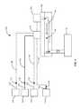
- FIG. 1illustrates a system 100 , including a reactor 102 .
- system 100includes a first precursor source 104 , a second precursor source 106 , a barrier layer precursor source 108 , a purge gas source 110 , an optional mixer 112 , an optional intake plenum 114 , and a vacuum source 116 .
- Sources 104 - 110may be coupled to mixer 112 or reactor 102 using lines 118 - 132 and valves 134 - 140 .
- Reactor 102may be a standalone reactor or part of a cluster tool. Further, reactor 102 may be dedicated to a particular process, such as a deposition process, or reactor 102 may be used for other processes—e.g., for layer passivation and/or etch processing.
- reactor 102may include a reactor typically used for atomic layer deposition (ALD) processing, such as a Pulsar 3000, available from ASM, and may include direct plasma, and/or remote plasma apparatus. Using a plasma may enhance the reactivity of one or more precursors.
- ALDatomic layer deposition
- Pulsar 3000available from ASM
- reactor 102includes a reactor suitable for ALD deposition of a dielectric material onto a substrate 142 .
- An exemplary ALD reactor suitable for system 100is described in United States Patent Application Publication No. US 2012/0266821, the contents of which are hereby incorporated herein by reference, to the extent such contents do not conflict with the present disclosure.
- An operating pressure of a reaction chamber 144 of reactor 102may vary in accordance with various factors.
- Reactor 102may be configured to operate at near atmospheric pressure or at lower pressures.
- an operating pressure of reactor 102 during deposition and purge stepsrange from about 0.01 Ton to about 100 Torr or about 1 Torr to about 5 Torr.
- first precursors for precursor source 104include, for example, one or more organometallic compounds or metal halide compounds.
- precursor sourceincludes one or more compounds selected from the group consisting of hafnium chloride (HfCl 4 ) and trimethylaluminum (TMA).
- Exemplary second precursors for precursor source 106include oxidants, such as oxygen, activated oxygen, ozone, water, or alcohol.
- precursor source 106includes water.
- Exemplary precursors for barrier layer source 108may include one or more precursors that react with adsorbed or absorbed material from source 104 and/or source 106 to form a less volatile compound.
- Suitable precursors for source 108include transition metal oxide, transition metal nitride, transition metal oxynitride, and transition metal carbide material precursors.
- precursor source 108includes a metal halide, such as HfCl 4 .
- Purge gas source 110may include any suitable purge or carrier gas.
- Exemplary gassesinclude nitrogen, argon, helium, and hydrogen.
- System 100may include a gas distribution system.
- An exemplary gas distribution systemwhich allows for fast switching between gasses (e.g., from sources 104 - 110 ) is set forth U.S. Pat. No. 8,152,922 to Schmidt et al., issued Apr. 10, 2012, entitled “Gas Mixer and Manifold Assembly for ALD Reactor,” the contents of which are hereby incorporated herein by reference, to the extent the contents do not conflict with the present disclosure.
- the gas distribution systemmay be used to, for example, mix a precursor gas and a carrier gas (which may be the same or different from a purge gas from purge gas source 108 ) prior to the gasses reaching plenum 114 or reactor 102 .
- reactors in accordance with alternative embodimentsmay include a vertical flow, for example, flow emanating from a showerhead and flowing substantially downward onto a substrate.
- An exemplary ALD deposition process using a systemincludes exposing a surface of substrate 142 within reaction chamber 144 of reactor 102 to a first precursor (e.g., an organometallic compound or a metal halide compound from source 104 ) that reacts with a species on a surface of substrate 142 to form a first surface species, purging the first precursor (e.g., using a purge gas from source 110 ), exposing the first surface species to a second precursor (e.g., an oxidant, such as water, from source 106 ) to form a second surface species, and purging the second precursor from the reaction chamber.
- a first precursore.g., an organometallic compound or a metal halide compound from source 104
- purging the first precursore.g., using a purge gas from source 110
- a second precursore.g., an oxidant, such as water, from source 106
- an exemplary ALD sequencesmay begin with exposure to an oxidant, followed by a purge, which is followed by exposure to a second precursor, which is followed by a purge.
- a precursor gasmay be mixed with a carrier gas, such as a purge gas from source 110 , at mixer 112 , and the mixture of the precursor and the carrier can be introduced into reaction chamber 144 using plenum 114 .
- the direction of the flow of the precursor and purge gasis generally indicated by the arrows in FIG. 1 .
- films formed using this techniquemay adsorb or absorb a precursor (e.g., from source 104 or 106 ) that may then outgas as the film is exposed to the other precursor.
- a precursore.g., from source 104 or 106
- a filmsuch as lanthanum oxide, magnesium oxide, barium oxide, and strontium oxide may be hygroscopic.
- waterif water is used as an oxidant, the water may be absorbed by the deposited film and may not adequately be purged during a purge cycle. The water may therefore outgas during a step of exposing a substrate to another precursor.
- this undesired outgassing of a precursoroccurs as the film is exposed another other precursor, high particle counts and reduced uniformity of film deposited onto the substrate may result.
- FIG. 2illustrates a method 200 of reducing outgassing of a substance.
- Method 200includes the steps of providing a gas-phase reactor having a reaction chamber (step 202 ), forming a barrier layer on a surface of the reaction chamber to mitigate outgassing of one or more gasses (step 204 ), depositing material onto a surface of a substrate within the reaction chamber (step 206 ), and removing the substrate from the reaction chamber (step 208 ).
- the methodproduces films having relatively low particle counts—e.g., less than 10 particles having a size of greater than 32 nm on a 300 mm substrate. Additionally or alternatively, the method produces films having non-uniformity values of less than one percent one sigma.
- Step 202includes providing a gas-phase reactor, such as reactor 102 of system 100 .
- the reactormay include an ALD reactor, such as a horizontal flow reactor.
- the reactormay operate at a pressure of about 0.01 Torr to about 100 Torr or about 1 Torr to about 5 Torr and a temperature of about 100° C. to about 600° C. or about 200° C. to about 350° C.
- a barrier layeris deposited onto the wetted surfaces or portions thereof within the reactor during step 204 .
- wetted surfaces of the reactorrefer to surfaces within the reactor that are exposed to the deposition gasses, such as precursors from sources 104 and 106 .
- Exemplary barrier layersinclude transition metal oxides, nitrides, oxynitrides, and carbides, as well as silicon oxide and aluminum oxide.
- the barrier layerincludes material selected from one or more of TiO 2 , TiN, TiON, TiC, Ta 2 O 5 , HlO 2 , SiO 2 , and Al 2 O 3 .
- a barrier layeris formed by reacting a precursor (e.g., from source 108 ) with a species (e.g., an oxidant) to form the barrier layer.
- a thickness of a barrier layer deposited during step 204may vary in accordance with, for example, the material deposited onto a surface of a substrate, a thickness of the material deposited during step 204 , a number of substrates processed during step 206 , and the like.
- a thickness of the barrier layermay be greater than one monolayer, greater than two monolayers, or between about one monolayer and about 50 ⁇ , about 5 ⁇ to about 20 ⁇ , or about 10 ⁇ to about 20 ⁇ .
- step 206material is deposited onto a surface of a substrate, such as substrate 142 .
- the surface of the substratemay have any suitable topography, including planar and/or non-planar surfaces that are exposed for deposition, and the substrate may include layers of various materials, such as materials used to form semiconductor and/or photonic devices.
- a surfacemay include a top surface or a portion thereof (including topology) of a semiconductor or photonic device workpiece or wafer.
- Step 206may suitably include depositing material using an ALD process.
- step 206may include the substeps of providing a first precursor (e.g., from source 104 ) to the reaction chamber, the first precursor reacting with a surface of the substrate to form a first surface species, purging the first precursor from the reaction chamber (e.g., using a purge gas from source 110 ), providing a second precursor (e.g., from source 106 ) to the reaction chamber to react with the first surface species to form a second surface species, and purging the second precursor from the reaction chamber.
- a first precursore.g., from source 104
- purging the first precursor from the reaction chambere.g., using a purge gas from source 110
- providing a second precursore.g., from source 106
- the substrateis removed from the reaction chamber.
- a substrate supported on a substrate support during step 204can be removed from reaction chamber 144 of reactor 102 by moving the support to an unload position and then removing the substrate from the reactor.
- materialmay be deposited onto multiple substrates, concurrently or sequentially during step 206 and removed from the reactor during step 208 . Steps 204 - 208 may be repeated a desired number of times.
- System 300is similar to system 100 , except system 300 includes a scavenging precursor source 302 for providing a scavenging precursor to reaction chamber 144 of reactor 102 .
- Exemplary scavenging precursors suitable for use with exemplary embodiments of the disclosureinclude metal halides, such as metal chlorides, and organometallic compounds.
- scavenging precursor source 302includes hafnium chloride or silicon chloride.
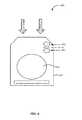
- FIG. 4illustrates a portion 400 of an interior of a reaction chamber, such as chamber 144 , which includes a first dose front monitoring device 402 and a second dose front monitoring device 404 located upstream of substrate 142 (or a location where substrate 142 would reside).
- exemplary dose front monitoring devicesinclude quartz crystal microbalances.
- the dose front monitoring devicesmay be mounted onto a lower portion 304 of reactor 102 and within reaction chamber 144 .
- the dose front monitoring devicesmay be used to tune process conditions, such that wetted surfaces of a reaction chamber that are upstream of the substrate can be exposed to the scavenging precursor, and all or nearly all of the scavenging precursor is consumed (e.g., reacts with) a species on the reaction chamber surface prior to reaching substrate 142 .
- the systemmay be tuned, such that a Stokes front of the scavenging precursor substantially falls to zero upstream of (e.g., near) substrate 142 . This allows the scavenging precursor to be used during a deposition process, rather than removing a substrate prior to exposing the reaction chamber to the scavenging precursor.
- FIG. 5illustrates another example of portion 400 , in which the dose front monitors are located further apart.
- monitor 404is located downstream of substrate 142 .
- additional and/or more complex calculationsmay be required to tune the reactor, such that all or nearly all of the scavenging precursor is consumed prior to reaching substrate 142 .
- FIG. 6illustrates a method 600 of reducing outgassing of a substance within a reaction chamber in accordance with additional exemplary embodiments of the disclosure.
- Method 600includes the steps of providing a gas-phase reactor having a reaction chamber (step 602 ), depositing material onto a surface or a substrate within the reaction chamber (step 604 ), and providing a scavenging precursor to the reaction chamber to react with the material on a surface of the reaction chamber (step 606 ).
- Providing a gas-phase reactor step 602may include providing any suitable reactor, such as the reactors disclosed herein.
- step 602includes providing an ALD reactor.
- step 604material may be deposited using, for example, an ALD process.
- step 604may include providing a first precursor to the reaction chamber to react with a surface of the substrate to form a first surface species, purging the first precursor from the reaction chamber, providing a second precursor to the reaction chamber to react with the first surface species to form a second surface species, and purging the second precursor from the reaction chamber.
- FIG. 7illustrates a process 700 , which includes an exemplary combination of steps 604 and 606 .
- process 700includes providing a first precursor to the reaction chamber to react with a surface of a substrate to form a first surface species (step 702 ), providing a scavenging precursor to the reaction chamber to react with the material on a surface of the reaction chamber—e.g., upstream of the substrate (step 704 ), purging the first precursor and the scavenging precursor from the reaction chamber (step 706 ), providing a second precursor to the reaction chamber to react with the first surface species to form a second surface species (step 708 ), and purging the second precursor from the reaction chamber (step 710 ).
- Step 704may include providing the scavenging precursor, such that all or nearly all of the scavenging precursor is consumed prior to reaching the substrate.
- Process 700may be repeated a desired number of times until a desired thickness of material is formed on a substrate.
- the precursors and purge gasses used for this processmay include any of the precursors and purge gases noted herein.
- FIG. 8illustrates another process 800 , which includes an alternative exemplary combination of steps 604 and 606 .
- Process 800is similar to process 700 , except process 800 includes an additional purge step 804 .
- Steps 802 , 806 , 808 , 810 , and 812may correspond to steps 702 - 710 , respectively, of process 700 , except step 808 may be shorter in duration and/or be at higher pressure, since less precursor material may be removed during this step, compared to step 706 .
Landscapes
- Chemical & Material Sciences (AREA)
- Engineering & Computer Science (AREA)
- Chemical Kinetics & Catalysis (AREA)
- General Chemical & Material Sciences (AREA)
- Materials Engineering (AREA)
- Mechanical Engineering (AREA)
- Metallurgy (AREA)
- Organic Chemistry (AREA)
- Physics & Mathematics (AREA)
- Condensed Matter Physics & Semiconductors (AREA)
- General Physics & Mathematics (AREA)
- Manufacturing & Machinery (AREA)
- Computer Hardware Design (AREA)
- Microelectronics & Electronic Packaging (AREA)
- Power Engineering (AREA)
- Chemical Vapour Deposition (AREA)
Abstract
Description
The present disclosure generally relates to gas-phase reaction methods and systems. More particularly, the disclosure relates to methods and systems to reduce outgassing of materials in a gas-phase reaction chamber.
Electronic devices, such as semiconductor devices, and photonic devices, such as light emitting and solar devices, are often formed by, among other things, depositing thin films of materials onto a substrate. Techniques for depositing films include atomic layer deposition (ALD). ALD may be desirable for various applications, because ALD processes are self-limiting, allowing precise, conformal deposition of material onto a substrate.
Atomic layer deposition typically includes gas-phase deposition of a film using two or more precursors, wherein one or more of the precursors may be activated, using, for example, a direct or remote plasma. A typical ALD process includes deposition using two precursors. In this case, a sequence often includes exposing a surface of a substrate to a first precursor to react with species on the surface of the substrate in a reaction chamber, purging the reaction chamber to remove the first precursor, exposing the surface of the substrate to a second precursor to react with species from the first precursor in the reaction chamber, and removing the second precursor from the reaction chamber. If each precursor is not sufficiently purged prior to the introduction of the other precursor into the reaction chamber, undesired gas-phase reactions may occur, which may, in turn, cause undesired particle formation or non-uniformity of the deposited film. Additionally or alternatively, insufficient purging of a precursor can result in depletion of a subsequently-introduced precursor.
During an ALD deposition process, one or more of the precursors may adsorb onto or be absorbed into a film formed on a surface of the reaction chamber and subsequently outgas during a cycle in which the other precursor is introduced into the reaction chamber. In this case, undesired gas-phase reactions may occur as one precursor outgasses as the other flows through the reaction chamber.
By way of example, when ALD is used to form a metal oxide film on a surface of a substrate, a method to form the metal oxide film may include exposing the substrate surface to a metal-containing precursor to react with chemical species on the substrate surface, purging the reaction chamber, exposing the substrate surface to an oxidant, such as oxygen, activated oxygen, ozone, water, or alcohol, and then purging the reaction chamber. These steps are repeated until a desired amount of the metal oxide is formed on the surface of the substrate. During these steps, the metal oxide film material is also deposited onto surfaces on the reaction chamber—in addition to the substrate surface. If the oxidant is absorbed into or adsorbed onto the material deposited onto the surface of a reaction chamber, the oxidant may not be completely purged from the reaction chamber during a purge step, and may therefore outgas during a subsequent step of exposing the substrate surface to a metal-containing precursor. As the oxidant outgasses, it may react with the metal-containing precursor during the step of exposing the substrate surface to a metal-containing precursor, resulting in undesired non-uniformity of the film across the substrate surface and/or particle formation within the reaction chamber.
To mitigate the outgassing of a precursor, the ALD process may be run at a relatively low pressure—e.g., less than 0.01 Torr—to enhance purging of the precursors. However, reducing the operating pressure of the reaction chamber to such low pressures generally decreases the throughput of the ALD process, and thus systems and methods operating at these pressures are not well suited for production of devices. Accordingly, improved methods and systems for mitigating outgassing from a reaction chamber during gas-phase reactions are desired.
Various embodiments of the present disclosure relate to methods and systems for mitigating outgassing of substances within a reaction chamber of a reactor. While the ways in which various embodiments of the disclosure address the drawbacks of the prior art methods and systems are discussed in more detail below, in general, the present disclosure provides systems and methods for providing a barrier layer, using a scavenging agent to react with one or more substances that might otherwise outgas, or otherwise blocking a substance within a reaction chamber to thereby mitigate or prevent outgassing of the substance(s) during subsequent processing within the reaction chamber.
In accordance with various embodiments of the disclosure, methods of reducing outgassing of a substance include the steps of providing a gas-phase reactor having a reaction chamber, forming a barrier layer on a surface within the reaction chamber, depositing material onto a surface of a substrate within the reaction chamber, and removing the substrate from the reaction chamber. The barrier layer may include, for example, a transition metal oxide (e.g., TiO2, Ta2O5, HfO2, or Al2O3or SiO2), a transition metal nitride (e.g., TiN), a transition metal oxynitride (e.g., TiON), and/or a transition metal carbide (e.g., TiC). A thickness of the barrier layer may vary according to application, and may be greater than one monolayer, greater than two monolayers, or between about one monolayer and about 50 Å, about 5 Å and about 20 Å, or about 10 Å and about 20 Å. In accordance with various aspects of these embodiments, the step of providing a gas-phase reactor comprises providing an atomic layer deposition (ALD) reactor. In accordance with further aspects, the step of depositing includes providing a first precursor to the reaction chamber, the first precursor reacting with a surface of the substrate to form a first surface species, purging the first precursor from the reaction chamber—e.g., using low pressure and/or a carrier gas, providing a second precursor to the reaction chamber to react with the first surface species to form a second surface species, and purging the second precursor from the reaction chamber. The methods may be particularly useful when the material deposited onto the substrate (and onto a surface within a reaction chamber) includes hygroscopic material, such as lanthanum oxide, magnesium oxide, barium oxide, strontium oxide, or other materials that tend to absorb or adsorb one or more of the precursors. Exemplary methods improve thickness uniformity of material deposited onto the substrate, increase a number of runs within the reaction chamber between cleaning cycles, and produce films of higher quality, compared to similar films produced without forming the barrier layer within the reaction chamber.
In accordance with additional embodiments of the disclosure, a system for depositing material onto a substrate and for mitigating outgassing of a substance within a reaction chamber includes a reactor, such as an ALD reactor, including a reaction chamber, a first precursor source fluidly coupled to the reaction chamber, a second precursor source fluidly coupled to the reaction chamber, a purge gas fluidly coupled to the reaction chamber, and a barrier layer precursor fluidly coupled to the reaction chamber. In accordance with exemplary aspects of these embodiments, the system is configured to form a barrier layer on a surface within the reaction chamber after a substrate is removed from the reaction chamber or before the substrate enters the reaction chamber. In accordance with further aspects, the barrier layer precursor may be selected from, for example, one or more of transition metal oxide precursors, transition metal nitride precursors, transition metal oxynitride precursors, transition metal carbide precursors, silicon oxide precursors, and aluminum oxide precursors.
In accordance with additional embodiments of the disclosure, methods of reducing outgassing of a substance within a reaction chamber include the steps of providing a gas-phase reactor having a reaction chamber, depositing material onto a surface of a substrate within the reaction chamber (and onto a surface within the reaction chamber), and providing a scavenging precursor to the reaction chamber to react with the material on a surface of the reaction chamber. In accordance with various aspects of these embodiments, the scavenging gas is or substantially is consumed or depleted prior to reaching the substrate or the substrate holder—e.g., using dose control. The scavenging precursor may be, for example, a metal halide or an organometallic compound, such as hafnium chloride, silicon chloride, zirconium chloride, or TMA. In accordance with exemplary aspects of these embodiments, the step of depositing material onto a surface includes providing a first precursor to the reaction chamber to react with a surface of the substrate to form a first surface species, purging the first precursor from the reaction chamber, providing a second precursor to the reaction chamber to react with the first surface species to form a second surface species and purging the second precursor. In these cases, the step of providing a scavenging precursor may occur after the step of providing a first precursor and/or before the step of purging the first precursor. Alternatively, the step of providing a scavenging precursor may occur after the step of purging the first precursor. A method may also include a step of purging the scavenging precursor—e.g., prior to the step of providing the second precursor. In accordance with various aspects of these embodiments, the methods may include a step of dose front monitoring, which allows tuning of a process to mitigate or prevent the scavenging precursor from reacting with a surface on the substrate. In other words, the method may be tuned to consume all or nearly all of the scavenging precursor upstream of the substrate.
In accordance with additional embodiments of the disclosure, a system for depositing material onto a substrate and for mitigating outgassing of a substance within a reaction chamber includes a reactor, such as an ALD reactor, including a reaction chamber, a first precursor source fluidly coupled to the reaction chamber, a second precursor source fluidly coupled to the reaction chamber, a purge gas fluidly coupled to the reaction chamber, and a scavenging precursor source fluidly coupled to the reaction chamber. In accordance with exemplary aspects of these embodiments, the reaction chamber is exposed to a first precursor, and after the reaction chamber is exposed to the first precursor, the reaction chamber is exposed to a scavenging precursor, and after the reaction chamber is exposed to the scavenging precursor, the reaction chamber is exposed to a second precursor. Systems in accordance with these embodiments may include dose front monitoring devices, such as one or more quartz crystal microbalances to tune the system, such that all or nearly all of the scavenging precursor is consumed upstream of the substrate.
Both the foregoing summary and the following detailed description are exemplary and explanatory only and are not restrictive of the disclosure or the claimed invention
A more complete understanding of the embodiments of the present disclosure may be derived by referring to the detailed description and claims when considered in connection with the following illustrative figures.
It will be appreciated that elements in the figures are illustrated for simplicity and clarity and have not necessarily been drawn to scale. For example, the dimensions of some of the elements in the figures may be exaggerated relative to other elements to help to improve the understanding of illustrated embodiments of the present disclosure.
The description of exemplary embodiments of methods and systems provided below is merely exemplary and is intended for purposes of illustration only; the following description is not intended to limit the scope of the disclosure or the claims. Moreover, recitation of multiple embodiments having stated features is not intended to exclude other embodiments having additional features or other embodiments incorporating different combinations of the stated features.
The present disclosure generally relates to gas-phase reactors, systems and methods. More particularly, the disclosure relates to reactors, systems, and methods that mitigate outgassing of substances from an interior surface of a reaction chamber—e.g., mitigate outgassing from material deposited onto an interior surface of a reaction chamber.
Exemplary first precursors forprecursor source 104 include, for example, one or more organometallic compounds or metal halide compounds. By way of examples, precursor source includes one or more compounds selected from the group consisting of hafnium chloride (HfCl4) and trimethylaluminum (TMA).
Exemplary second precursors forprecursor source 106 include oxidants, such as oxygen, activated oxygen, ozone, water, or alcohol. By way of particular examples,precursor source 106 includes water.
Exemplary precursors forbarrier layer source 108 may include one or more precursors that react with adsorbed or absorbed material fromsource 104 and/orsource 106 to form a less volatile compound. Suitable precursors forsource 108 include transition metal oxide, transition metal nitride, transition metal oxynitride, and transition metal carbide material precursors. By way of examples,precursor source 108 includes a metal halide, such as HfCl4.
An exemplary ALD deposition process using a system, such assystem 100, includes exposing a surface ofsubstrate 142 withinreaction chamber 144 ofreactor 102 to a first precursor (e.g., an organometallic compound or a metal halide compound from source104) that reacts with a species on a surface ofsubstrate 142 to form a first surface species, purging the first precursor (e.g., using a purge gas from source110), exposing the first surface species to a second precursor (e.g., an oxidant, such as water, from source106) to form a second surface species, and purging the second precursor from the reaction chamber. Alternatively, an exemplary ALD sequences may begin with exposure to an oxidant, followed by a purge, which is followed by exposure to a second precursor, which is followed by a purge. In the system illustrated inFIG. 1 , a precursor gas may be mixed with a carrier gas, such as a purge gas fromsource 110, atmixer 112, and the mixture of the precursor and the carrier can be introduced intoreaction chamber 144 usingplenum 114. The direction of the flow of the precursor and purge gas is generally indicated by the arrows inFIG. 1 .
Several films formed using this technique may adsorb or absorb a precursor (e.g., fromsource 104 or106) that may then outgas as the film is exposed to the other precursor. For example, a film such as lanthanum oxide, magnesium oxide, barium oxide, and strontium oxide may be hygroscopic. In this case, if water is used as an oxidant, the water may be absorbed by the deposited film and may not adequately be purged during a purge cycle. The water may therefore outgas during a step of exposing a substrate to another precursor. When this undesired outgassing of a precursor occurs as the film is exposed another other precursor, high particle counts and reduced uniformity of film deposited onto the substrate may result.
Step202 includes providing a gas-phase reactor, such asreactor 102 ofsystem 100. As noted above, the reactor may include an ALD reactor, such as a horizontal flow reactor. The reactor may operate at a pressure of about 0.01 Torr to about 100 Torr or about 1 Torr to about 5 Torr and a temperature of about 100° C. to about 600° C. or about 200° C. to about 350° C.
To mitigate undesired outgassing of a substance, such as a first precursor or a second precursor that may be absorbed by or adsorbed onto material deposited onto an interior surface of a reaction chamber, a barrier layer is deposited onto the wetted surfaces or portions thereof within the reactor duringstep 204. As used herein, wetted surfaces of the reactor refer to surfaces within the reactor that are exposed to the deposition gasses, such as precursors fromsources
A thickness of a barrier layer deposited duringstep 204 may vary in accordance with, for example, the material deposited onto a surface of a substrate, a thickness of the material deposited duringstep 204, a number of substrates processed duringstep 206, and the like. By way of examples, a thickness of the barrier layer may be greater than one monolayer, greater than two monolayers, or between about one monolayer and about 50 Å, about 5 Å to about 20 Å, or about 10 Å to about 20 Å.
Duringstep 206, material is deposited onto a surface of a substrate, such assubstrate 142. The surface of the substrate may have any suitable topography, including planar and/or non-planar surfaces that are exposed for deposition, and the substrate may include layers of various materials, such as materials used to form semiconductor and/or photonic devices. For example, a surface may include a top surface or a portion thereof (including topology) of a semiconductor or photonic device workpiece or wafer. Step206 may suitably include depositing material using an ALD process. In this case, step206 may include the substeps of providing a first precursor (e.g., from source104) to the reaction chamber, the first precursor reacting with a surface of the substrate to form a first surface species, purging the first precursor from the reaction chamber (e.g., using a purge gas from source110), providing a second precursor (e.g., from source106) to the reaction chamber to react with the first surface species to form a second surface species, and purging the second precursor from the reaction chamber. These steps may be repeated a desired number of times until a desired or predetermined amount of material is formed on the surface of the substrate.
Atstep 208, the substrate is removed from the reaction chamber. By way of example, a substrate supported on a substrate support duringstep 204 can be removed fromreaction chamber 144 ofreactor 102 by moving the support to an unload position and then removing the substrate from the reactor. Although illustrated asprocess 200 progressing to step208, material may be deposited onto multiple substrates, concurrently or sequentially duringstep 206 and removed from the reactor duringstep 208. Steps204-208 may be repeated a desired number of times.
Turning now toFIG. 3 , asystem 300, in accordance with additional embodiments of the disclosure, is illustrated.System 300 is similar tosystem 100, exceptsystem 300 includes a scavengingprecursor source 302 for providing a scavenging precursor toreaction chamber 144 ofreactor 102.
Exemplary scavenging precursors suitable for use with exemplary embodiments of the disclosure include metal halides, such as metal chlorides, and organometallic compounds. By way of particular examples, scavengingprecursor source 302 includes hafnium chloride or silicon chloride.
Exemplary systems in accordance with various embodiments of the disclosure include one or more dose front monitoring devices to enable tuning of the system.FIG. 4 illustrates aportion 400 of an interior of a reaction chamber, such aschamber 144, which includes a first dosefront monitoring device 402 and a second dosefront monitoring device 404 located upstream of substrate142 (or a location wheresubstrate 142 would reside). Exemplary dose front monitoring devices include quartz crystal microbalances.
The dose front monitoring devices may be mounted onto alower portion 304 ofreactor 102 and withinreaction chamber 144. The dose front monitoring devices may be used to tune process conditions, such that wetted surfaces of a reaction chamber that are upstream of the substrate can be exposed to the scavenging precursor, and all or nearly all of the scavenging precursor is consumed (e.g., reacts with) a species on the reaction chamber surface prior to reachingsubstrate 142. For example, the system may be tuned, such that a Stokes front of the scavenging precursor substantially falls to zero upstream of (e.g., near)substrate 142. This allows the scavenging precursor to be used during a deposition process, rather than removing a substrate prior to exposing the reaction chamber to the scavenging precursor.
Providing a gas-phase reactor step 602 may include providing any suitable reactor, such as the reactors disclosed herein. In accordance with various examples,step 602 includes providing an ALD reactor.
Duringstep 604, material may be deposited using, for example, an ALD process. In this case, step604 may include providing a first precursor to the reaction chamber to react with a surface of the substrate to form a first surface species, purging the first precursor from the reaction chamber, providing a second precursor to the reaction chamber to react with the first surface species to form a second surface species, and purging the second precursor from the reaction chamber.
Although illustrated asseparate steps steps FIG. 7 illustrates aprocess 700, which includes an exemplary combination ofsteps
In the illustrated example,process 700 includes providing a first precursor to the reaction chamber to react with a surface of a substrate to form a first surface species (step702), providing a scavenging precursor to the reaction chamber to react with the material on a surface of the reaction chamber—e.g., upstream of the substrate (step704), purging the first precursor and the scavenging precursor from the reaction chamber (step706), providing a second precursor to the reaction chamber to react with the first surface species to form a second surface species (step708), and purging the second precursor from the reaction chamber (step710). Step704 may include providing the scavenging precursor, such that all or nearly all of the scavenging precursor is consumed prior to reaching the substrate.Process 700 may be repeated a desired number of times until a desired thickness of material is formed on a substrate. And, the precursors and purge gasses used for this process may include any of the precursors and purge gases noted herein.
Although exemplary embodiments of the present disclosure are set forth herein, it should be appreciated that the disclosure is not so limited. For example, although the system and method are described in connection with various specific chemistries, the disclosure is not necessarily limited to these examples. Further, although methods are illustrated in a particular sequence, the method is not limited to such sequence of steps, unless indicated herein to the contrary. Various modifications, variations, and enhancements of the system and method set forth herein may be made without departing from the spirit and scope of the present disclosure.
The subject matter of the present disclosure includes all novel and nonobvious combinations and subcombinations of the various processes, systems and configurations, and other features, functions, acts, and/or properties disclosed herein, as well as any and all equivalents thereof.
Claims (11)
1. A method of reducing outgassing of a substance within a reaction chamber, the method comprising the steps of:
providing a gas-phase reactor having a reaction chamber;
depositing material onto a surface of a substrate within the reaction chamber; and
providing a scavenging precursor to the reaction chamber to react with the material on a surface of the reaction chamber that is upstream of the substrate, wherein the scavenging precursor is substantially consumed or is consumed prior to reaching the substrate.
2. The method ofclaim 1 , wherein the scavenging precursor is selected from the group consisting of metal halides and organometallic compounds.
3. The method ofclaim 1 , wherein the scavenging precursor is selected from the group consisting of HfCl4and SiCl4, and TMA.
4. The method ofclaim 1 , wherein the step of depositing material onto a surface of a substrate comprises:
providing a first precursor to the reaction chamber to react with a surface of the substrate to form a first surface species;
purging the first precursor from the reaction chamber;
providing a second precursor to the reaction chamber to react with the first surface species to form a second surface species; and
purging the second precursor from the reaction chamber.
5. The method ofclaim 4 , wherein the step of providing a scavenging precursor occurs after the step of providing a first precursor.
6. The method ofclaim 5 , wherein the step of providing a scavenging precursor occurs before the step of purging the first precursor.
7. The method ofclaim 4 , wherein the step of providing a scavenging precursor occurs after the step of purging the first precursor.
8. The method ofclaim 7 , further comprising a step of purging the scavenging precursor.
9. The method ofclaim 8 , wherein the step of purging the scavenging precursor occurs before the step of providing a second precursor.
10. The method ofclaim 1 , further comprising a step of dose front monitoring to monitor dosing of the scavenging precursor at a front of the scavenging precursor flow.
11. The method ofclaim 10 , wherein the step of dose front monitoring is used to tune process conditions to consume the scavenging precursor prior to the scavenging precursor reaching the substrate.
Priority Applications (4)
| Application Number | Priority Date | Filing Date | Title |
|---|---|---|---|
| US13/941,134US8993054B2 (en) | 2013-07-12 | 2013-07-12 | Method and system to reduce outgassing in a reaction chamber |
| TW103123439ATWI670393B (en) | 2013-07-12 | 2014-07-08 | Method and system to reduce outgassing in a reaction chamber |
| KR1020140086902AKR102186335B1 (en) | 2013-07-12 | 2014-07-10 | Method and system to reduce outgassing in a reaction chamber |
| US14/606,364US9790595B2 (en) | 2013-07-12 | 2015-01-27 | Method and system to reduce outgassing in a reaction chamber |
Applications Claiming Priority (1)
| Application Number | Priority Date | Filing Date | Title |
|---|---|---|---|
| US13/941,134US8993054B2 (en) | 2013-07-12 | 2013-07-12 | Method and system to reduce outgassing in a reaction chamber |
Related Child Applications (1)
| Application Number | Title | Priority Date | Filing Date |
|---|---|---|---|
| US14/606,364DivisionUS9790595B2 (en) | 2013-07-12 | 2015-01-27 | Method and system to reduce outgassing in a reaction chamber |
Publications (2)
| Publication Number | Publication Date |
|---|---|
| US20150017319A1 US20150017319A1 (en) | 2015-01-15 |
| US8993054B2true US8993054B2 (en) | 2015-03-31 |
Family
ID=52277288
Family Applications (2)
| Application Number | Title | Priority Date | Filing Date |
|---|---|---|---|
| US13/941,134ActiveUS8993054B2 (en) | 2013-07-12 | 2013-07-12 | Method and system to reduce outgassing in a reaction chamber |
| US14/606,364ActiveUS9790595B2 (en) | 2013-07-12 | 2015-01-27 | Method and system to reduce outgassing in a reaction chamber |
Family Applications After (1)
| Application Number | Title | Priority Date | Filing Date |
|---|---|---|---|
| US14/606,364ActiveUS9790595B2 (en) | 2013-07-12 | 2015-01-27 | Method and system to reduce outgassing in a reaction chamber |
Country Status (3)
| Country | Link |
|---|---|
| US (2) | US8993054B2 (en) |
| KR (1) | KR102186335B1 (en) |
| TW (1) | TWI670393B (en) |
Cited By (400)
| Publication number | Priority date | Publication date | Assignee | Title |
|---|---|---|---|---|
| US9096931B2 (en) | 2011-10-27 | 2015-08-04 | Asm America, Inc | Deposition valve assembly and method of heating the same |
| US9117866B2 (en) | 2012-07-31 | 2015-08-25 | Asm Ip Holding B.V. | Apparatus and method for calculating a wafer position in a processing chamber under process conditions |
| US9167625B2 (en) | 2011-11-23 | 2015-10-20 | Asm Ip Holding B.V. | Radiation shielding for a substrate holder |
| US9169975B2 (en) | 2012-08-28 | 2015-10-27 | Asm Ip Holding B.V. | Systems and methods for mass flow controller verification |
| US9177784B2 (en) | 2012-05-07 | 2015-11-03 | Asm Ip Holdings B.V. | Semiconductor device dielectric interface layer |
| US9202727B2 (en) | 2012-03-02 | 2015-12-01 | ASM IP Holding | Susceptor heater shim |
| US9228259B2 (en) | 2013-02-01 | 2016-01-05 | Asm Ip Holding B.V. | Method for treatment of deposition reactor |
| US9240412B2 (en) | 2013-09-27 | 2016-01-19 | Asm Ip Holding B.V. | Semiconductor structure and device and methods of forming same using selective epitaxial process |
| US9299595B2 (en) | 2012-06-27 | 2016-03-29 | Asm Ip Holding B.V. | Susceptor heater and method of heating a substrate |
| US9324811B2 (en) | 2012-09-26 | 2016-04-26 | Asm Ip Holding B.V. | Structures and devices including a tensile-stressed silicon arsenic layer and methods of forming same |
| US9340874B2 (en) | 2011-11-23 | 2016-05-17 | Asm Ip Holding B.V. | Chamber sealing member |
| US9341296B2 (en) | 2011-10-27 | 2016-05-17 | Asm America, Inc. | Heater jacket for a fluid line |
| US9384987B2 (en) | 2012-04-04 | 2016-07-05 | Asm Ip Holding B.V. | Metal oxide protective layer for a semiconductor device |
| US9396934B2 (en) | 2013-08-14 | 2016-07-19 | Asm Ip Holding B.V. | Methods of forming films including germanium tin and structures and devices including the films |
| US9394608B2 (en) | 2009-04-06 | 2016-07-19 | Asm America, Inc. | Semiconductor processing reactor and components thereof |
| US9404587B2 (en) | 2014-04-24 | 2016-08-02 | ASM IP Holding B.V | Lockout tagout for semiconductor vacuum valve |
| US9412564B2 (en) | 2013-07-22 | 2016-08-09 | Asm Ip Holding B.V. | Semiconductor reaction chamber with plasma capabilities |
| US9447498B2 (en) | 2014-03-18 | 2016-09-20 | Asm Ip Holding B.V. | Method for performing uniform processing in gas system-sharing multiple reaction chambers |
| US9455138B1 (en) | 2015-11-10 | 2016-09-27 | Asm Ip Holding B.V. | Method for forming dielectric film in trenches by PEALD using H-containing gas |
| US9478415B2 (en) | 2015-02-13 | 2016-10-25 | Asm Ip Holding B.V. | Method for forming film having low resistance and shallow junction depth |
| US9484191B2 (en) | 2013-03-08 | 2016-11-01 | Asm Ip Holding B.V. | Pulsed remote plasma method and system |
| US9543180B2 (en) | 2014-08-01 | 2017-01-10 | Asm Ip Holding B.V. | Apparatus and method for transporting wafers between wafer carrier and process tool under vacuum |
| US9558931B2 (en) | 2012-07-27 | 2017-01-31 | Asm Ip Holding B.V. | System and method for gas-phase sulfur passivation of a semiconductor surface |
| US9556516B2 (en) | 2013-10-09 | 2017-01-31 | ASM IP Holding B.V | Method for forming Ti-containing film by PEALD using TDMAT or TDEAT |
| US9589770B2 (en) | 2013-03-08 | 2017-03-07 | Asm Ip Holding B.V. | Method and systems for in-situ formation of intermediate reactive species |
| US9605343B2 (en) | 2013-11-13 | 2017-03-28 | Asm Ip Holding B.V. | Method for forming conformal carbon films, structures conformal carbon film, and system of forming same |
| US9605342B2 (en) | 2012-09-12 | 2017-03-28 | Asm Ip Holding B.V. | Process gas management for an inductively-coupled plasma deposition reactor |
| US9607837B1 (en) | 2015-12-21 | 2017-03-28 | Asm Ip Holding B.V. | Method for forming silicon oxide cap layer for solid state diffusion process |
| US9627221B1 (en) | 2015-12-28 | 2017-04-18 | Asm Ip Holding B.V. | Continuous process incorporating atomic layer etching |
| US9640416B2 (en) | 2012-12-26 | 2017-05-02 | Asm Ip Holding B.V. | Single-and dual-chamber module-attachable wafer-handling chamber |
| US9647114B2 (en) | 2015-08-14 | 2017-05-09 | Asm Ip Holding B.V. | Methods of forming highly p-type doped germanium tin films and structures and devices including the films |
| US9657845B2 (en) | 2014-10-07 | 2017-05-23 | Asm Ip Holding B.V. | Variable conductance gas distribution apparatus and method |
| US9659799B2 (en) | 2012-08-28 | 2017-05-23 | Asm Ip Holding B.V. | Systems and methods for dynamic semiconductor process scheduling |
| US9711345B2 (en) | 2015-08-25 | 2017-07-18 | Asm Ip Holding B.V. | Method for forming aluminum nitride-based film by PEALD |
| US9735024B2 (en) | 2015-12-28 | 2017-08-15 | Asm Ip Holding B.V. | Method of atomic layer etching using functional group-containing fluorocarbon |
| US9754779B1 (en) | 2016-02-19 | 2017-09-05 | Asm Ip Holding B.V. | Method for forming silicon nitride film selectively on sidewalls or flat surfaces of trenches |
| US9793115B2 (en) | 2013-08-14 | 2017-10-17 | Asm Ip Holding B.V. | Structures and devices including germanium-tin films and methods of forming same |
| US9793148B2 (en) | 2011-06-22 | 2017-10-17 | Asm Japan K.K. | Method for positioning wafers in multiple wafer transport |
| US9793135B1 (en) | 2016-07-14 | 2017-10-17 | ASM IP Holding B.V | Method of cyclic dry etching using etchant film |
| US9790595B2 (en) | 2013-07-12 | 2017-10-17 | Asm Ip Holding B.V. | Method and system to reduce outgassing in a reaction chamber |
| US9812320B1 (en) | 2016-07-28 | 2017-11-07 | Asm Ip Holding B.V. | Method and apparatus for filling a gap |
| US9859151B1 (en) | 2016-07-08 | 2018-01-02 | Asm Ip Holding B.V. | Selective film deposition method to form air gaps |
| US9887082B1 (en) | 2016-07-28 | 2018-02-06 | Asm Ip Holding B.V. | Method and apparatus for filling a gap |
| US9891521B2 (en) | 2014-11-19 | 2018-02-13 | Asm Ip Holding B.V. | Method for depositing thin film |
| US9892908B2 (en) | 2011-10-28 | 2018-02-13 | Asm America, Inc. | Process feed management for semiconductor substrate processing |
| US9890456B2 (en) | 2014-08-21 | 2018-02-13 | Asm Ip Holding B.V. | Method and system for in situ formation of gas-phase compounds |
| US9899291B2 (en) | 2015-07-13 | 2018-02-20 | Asm Ip Holding B.V. | Method for protecting layer by forming hydrocarbon-based extremely thin film |
| US9899405B2 (en) | 2014-12-22 | 2018-02-20 | Asm Ip Holding B.V. | Semiconductor device and manufacturing method thereof |
| US9905420B2 (en) | 2015-12-01 | 2018-02-27 | Asm Ip Holding B.V. | Methods of forming silicon germanium tin films and structures and devices including the films |
| US9909214B2 (en) | 2015-10-15 | 2018-03-06 | Asm Ip Holding B.V. | Method for depositing dielectric film in trenches by PEALD |
| US9916980B1 (en) | 2016-12-15 | 2018-03-13 | Asm Ip Holding B.V. | Method of forming a structure on a substrate |
| US9960072B2 (en) | 2015-09-29 | 2018-05-01 | Asm Ip Holding B.V. | Variable adjustment for precise matching of multiple chamber cavity housings |
| US10032628B2 (en) | 2016-05-02 | 2018-07-24 | Asm Ip Holding B.V. | Source/drain performance through conformal solid state doping |
| US10043661B2 (en) | 2015-07-13 | 2018-08-07 | Asm Ip Holding B.V. | Method for protecting layer by forming hydrocarbon-based extremely thin film |
| US10083836B2 (en) | 2015-07-24 | 2018-09-25 | Asm Ip Holding B.V. | Formation of boron-doped titanium metal films with high work function |
| US10087522B2 (en) | 2016-04-21 | 2018-10-02 | Asm Ip Holding B.V. | Deposition of metal borides |
| US10087525B2 (en) | 2015-08-04 | 2018-10-02 | Asm Ip Holding B.V. | Variable gap hard stop design |
| US10090316B2 (en) | 2016-09-01 | 2018-10-02 | Asm Ip Holding B.V. | 3D stacked multilayer semiconductor memory using doped select transistor channel |
| US10103040B1 (en) | 2017-03-31 | 2018-10-16 | Asm Ip Holding B.V. | Apparatus and method for manufacturing a semiconductor device |
| USD830981S1 (en) | 2017-04-07 | 2018-10-16 | Asm Ip Holding B.V. | Susceptor for semiconductor substrate processing apparatus |
| US10134757B2 (en) | 2016-11-07 | 2018-11-20 | Asm Ip Holding B.V. | Method of processing a substrate and a device manufactured by using the method |
| US10167557B2 (en) | 2014-03-18 | 2019-01-01 | Asm Ip Holding B.V. | Gas distribution system, reactor including the system, and methods of using the same |
| US10177025B2 (en) | 2016-07-28 | 2019-01-08 | Asm Ip Holding B.V. | Method and apparatus for filling a gap |
| US10179947B2 (en) | 2013-11-26 | 2019-01-15 | Asm Ip Holding B.V. | Method for forming conformal nitrided, oxidized, or carbonized dielectric film by atomic layer deposition |
| US10190213B2 (en) | 2016-04-21 | 2019-01-29 | Asm Ip Holding B.V. | Deposition of metal borides |
| US10211308B2 (en) | 2015-10-21 | 2019-02-19 | Asm Ip Holding B.V. | NbMC layers |
| US10229833B2 (en) | 2016-11-01 | 2019-03-12 | Asm Ip Holding B.V. | Methods for forming a transition metal nitride film on a substrate by atomic layer deposition and related semiconductor device structures |
| US10236177B1 (en) | 2017-08-22 | 2019-03-19 | ASM IP Holding B.V.. | Methods for depositing a doped germanium tin semiconductor and related semiconductor device structures |
| US10249577B2 (en) | 2016-05-17 | 2019-04-02 | Asm Ip Holding B.V. | Method of forming metal interconnection and method of fabricating semiconductor apparatus using the method |
| US10249524B2 (en) | 2017-08-09 | 2019-04-02 | Asm Ip Holding B.V. | Cassette holder assembly for a substrate cassette and holding member for use in such assembly |
| US10262859B2 (en) | 2016-03-24 | 2019-04-16 | Asm Ip Holding B.V. | Process for forming a film on a substrate using multi-port injection assemblies |
| US10269558B2 (en) | 2016-12-22 | 2019-04-23 | Asm Ip Holding B.V. | Method of forming a structure on a substrate |
| US10276355B2 (en) | 2015-03-12 | 2019-04-30 | Asm Ip Holding B.V. | Multi-zone reactor, system including the reactor, and method of using the same |
| US10283353B2 (en) | 2017-03-29 | 2019-05-07 | Asm Ip Holding B.V. | Method of reforming insulating film deposited on substrate with recess pattern |
| US10290508B1 (en) | 2017-12-05 | 2019-05-14 | Asm Ip Holding B.V. | Method for forming vertical spacers for spacer-defined patterning |
| US10312055B2 (en) | 2017-07-26 | 2019-06-04 | Asm Ip Holding B.V. | Method of depositing film by PEALD using negative bias |
| US10319588B2 (en) | 2017-10-10 | 2019-06-11 | Asm Ip Holding B.V. | Method for depositing a metal chalcogenide on a substrate by cyclical deposition |
| US10322384B2 (en) | 2015-11-09 | 2019-06-18 | Asm Ip Holding B.V. | Counter flow mixer for process chamber |
| US10340135B2 (en) | 2016-11-28 | 2019-07-02 | Asm Ip Holding B.V. | Method of topologically restricted plasma-enhanced cyclic deposition of silicon or metal nitride |
| US10343920B2 (en) | 2016-03-18 | 2019-07-09 | Asm Ip Holding B.V. | Aligned carbon nanotubes |
| US10367080B2 (en) | 2016-05-02 | 2019-07-30 | Asm Ip Holding B.V. | Method of forming a germanium oxynitride film |
| US10364496B2 (en) | 2011-06-27 | 2019-07-30 | Asm Ip Holding B.V. | Dual section module having shared and unshared mass flow controllers |
| US10381226B2 (en) | 2016-07-27 | 2019-08-13 | Asm Ip Holding B.V. | Method of processing substrate |
| US10378106B2 (en) | 2008-11-14 | 2019-08-13 | Asm Ip Holding B.V. | Method of forming insulation film by modified PEALD |
| US10381219B1 (en) | 2018-10-25 | 2019-08-13 | Asm Ip Holding B.V. | Methods for forming a silicon nitride film |
| US10388513B1 (en) | 2018-07-03 | 2019-08-20 | Asm Ip Holding B.V. | Method for depositing silicon-free carbon-containing film as gap-fill layer by pulse plasma-assisted deposition |
| US10388509B2 (en) | 2016-06-28 | 2019-08-20 | Asm Ip Holding B.V. | Formation of epitaxial layers via dislocation filtering |
| US10395919B2 (en) | 2016-07-28 | 2019-08-27 | Asm Ip Holding B.V. | Method and apparatus for filling a gap |
| US10403504B2 (en) | 2017-10-05 | 2019-09-03 | Asm Ip Holding B.V. | Method for selectively depositing a metallic film on a substrate |
| US10410943B2 (en) | 2016-10-13 | 2019-09-10 | Asm Ip Holding B.V. | Method for passivating a surface of a semiconductor and related systems |
| US10435790B2 (en) | 2016-11-01 | 2019-10-08 | Asm Ip Holding B.V. | Method of subatmospheric plasma-enhanced ALD using capacitively coupled electrodes with narrow gap |
| US10446393B2 (en) | 2017-05-08 | 2019-10-15 | Asm Ip Holding B.V. | Methods for forming silicon-containing epitaxial layers and related semiconductor device structures |
| US10458018B2 (en) | 2015-06-26 | 2019-10-29 | Asm Ip Holding B.V. | Structures including metal carbide material, devices including the structures, and methods of forming same |
| US10468262B2 (en) | 2017-02-15 | 2019-11-05 | Asm Ip Holding B.V. | Methods for forming a metallic film on a substrate by a cyclical deposition and related semiconductor device structures |
| US10468251B2 (en) | 2016-02-19 | 2019-11-05 | Asm Ip Holding B.V. | Method for forming spacers using silicon nitride film for spacer-defined multiple patterning |
| US10483099B1 (en) | 2018-07-26 | 2019-11-19 | Asm Ip Holding B.V. | Method for forming thermally stable organosilicon polymer film |
| US10501866B2 (en) | 2016-03-09 | 2019-12-10 | Asm Ip Holding B.V. | Gas distribution apparatus for improved film uniformity in an epitaxial system |
| US10504742B2 (en) | 2017-05-31 | 2019-12-10 | Asm Ip Holding B.V. | Method of atomic layer etching using hydrogen plasma |
| US10510536B2 (en) | 2018-03-29 | 2019-12-17 | Asm Ip Holding B.V. | Method of depositing a co-doped polysilicon film on a surface of a substrate within a reaction chamber |
| US10529542B2 (en) | 2015-03-11 | 2020-01-07 | Asm Ip Holdings B.V. | Cross-flow reactor and method |
| US10529554B2 (en) | 2016-02-19 | 2020-01-07 | Asm Ip Holding B.V. | Method for forming silicon nitride film selectively on sidewalls or flat surfaces of trenches |
| US10529563B2 (en) | 2017-03-29 | 2020-01-07 | Asm Ip Holdings B.V. | Method for forming doped metal oxide films on a substrate by cyclical deposition and related semiconductor device structures |
| US10535516B2 (en) | 2018-02-01 | 2020-01-14 | Asm Ip Holdings B.V. | Method for depositing a semiconductor structure on a surface of a substrate and related semiconductor structures |
| US10541333B2 (en) | 2017-07-19 | 2020-01-21 | Asm Ip Holding B.V. | Method for depositing a group IV semiconductor and related semiconductor device structures |
| US10559458B1 (en) | 2018-11-26 | 2020-02-11 | Asm Ip Holding B.V. | Method of forming oxynitride film |
| US10590535B2 (en) | 2017-07-26 | 2020-03-17 | Asm Ip Holdings B.V. | Chemical treatment, deposition and/or infiltration apparatus and method for using the same |
| US10600673B2 (en) | 2015-07-07 | 2020-03-24 | Asm Ip Holding B.V. | Magnetic susceptor to baseplate seal |
| US10607895B2 (en) | 2017-09-18 | 2020-03-31 | Asm Ip Holdings B.V. | Method for forming a semiconductor device structure comprising a gate fill metal |
| US10605530B2 (en) | 2017-07-26 | 2020-03-31 | Asm Ip Holding B.V. | Assembly of a liner and a flange for a vertical furnace as well as the liner and the vertical furnace |
| US10612137B2 (en) | 2016-07-08 | 2020-04-07 | Asm Ip Holdings B.V. | Organic reactants for atomic layer deposition |
| USD880437S1 (en) | 2018-02-01 | 2020-04-07 | Asm Ip Holding B.V. | Gas supply plate for semiconductor manufacturing apparatus |
| US10612136B2 (en) | 2018-06-29 | 2020-04-07 | ASM IP Holding, B.V. | Temperature-controlled flange and reactor system including same |
| US10643904B2 (en) | 2016-11-01 | 2020-05-05 | Asm Ip Holdings B.V. | Methods for forming a semiconductor device and related semiconductor device structures |
| US10643826B2 (en) | 2016-10-26 | 2020-05-05 | Asm Ip Holdings B.V. | Methods for thermally calibrating reaction chambers |
| US10658205B2 (en) | 2017-09-28 | 2020-05-19 | Asm Ip Holdings B.V. | Chemical dispensing apparatus and methods for dispensing a chemical to a reaction chamber |
| US10658181B2 (en) | 2018-02-20 | 2020-05-19 | Asm Ip Holding B.V. | Method of spacer-defined direct patterning in semiconductor fabrication |
| US10655221B2 (en) | 2017-02-09 | 2020-05-19 | Asm Ip Holding B.V. | Method for depositing oxide film by thermal ALD and PEALD |
| US10683571B2 (en) | 2014-02-25 | 2020-06-16 | Asm Ip Holding B.V. | Gas supply manifold and method of supplying gases to chamber using same |
| US10685834B2 (en) | 2017-07-05 | 2020-06-16 | Asm Ip Holdings B.V. | Methods for forming a silicon germanium tin layer and related semiconductor device structures |
| US10692741B2 (en) | 2017-08-08 | 2020-06-23 | Asm Ip Holdings B.V. | Radiation shield |
| US10707106B2 (en) | 2011-06-06 | 2020-07-07 | Asm Ip Holding B.V. | High-throughput semiconductor-processing apparatus equipped with multiple dual-chamber modules |
| US10714385B2 (en) | 2016-07-19 | 2020-07-14 | Asm Ip Holding B.V. | Selective deposition of tungsten |
| US10714350B2 (en) | 2016-11-01 | 2020-07-14 | ASM IP Holdings, B.V. | Methods for forming a transition metal niobium nitride film on a substrate by atomic layer deposition and related semiconductor device structures |
| US10714335B2 (en) | 2017-04-25 | 2020-07-14 | Asm Ip Holding B.V. | Method of depositing thin film and method of manufacturing semiconductor device |
| US10714315B2 (en) | 2012-10-12 | 2020-07-14 | Asm Ip Holdings B.V. | Semiconductor reaction chamber showerhead |
| US10734244B2 (en) | 2017-11-16 | 2020-08-04 | Asm Ip Holding B.V. | Method of processing a substrate and a device manufactured by the same |
| US10734497B2 (en) | 2017-07-18 | 2020-08-04 | Asm Ip Holding B.V. | Methods for forming a semiconductor device structure and related semiconductor device structures |
| US10731249B2 (en) | 2018-02-15 | 2020-08-04 | Asm Ip Holding B.V. | Method of forming a transition metal containing film on a substrate by a cyclical deposition process, a method for supplying a transition metal halide compound to a reaction chamber, and related vapor deposition apparatus |
| US10755922B2 (en) | 2018-07-03 | 2020-08-25 | Asm Ip Holding B.V. | Method for depositing silicon-free carbon-containing film as gap-fill layer by pulse plasma-assisted deposition |
| US10770286B2 (en) | 2017-05-08 | 2020-09-08 | Asm Ip Holdings B.V. | Methods for selectively forming a silicon nitride film on a substrate and related semiconductor device structures |
| US10770336B2 (en) | 2017-08-08 | 2020-09-08 | Asm Ip Holding B.V. | Substrate lift mechanism and reactor including same |
| US10767789B2 (en) | 2018-07-16 | 2020-09-08 | Asm Ip Holding B.V. | Diaphragm valves, valve components, and methods for forming valve components |
| US10797133B2 (en) | 2018-06-21 | 2020-10-06 | Asm Ip Holding B.V. | Method for depositing a phosphorus doped silicon arsenide film and related semiconductor device structures |
| US10804098B2 (en) | 2009-08-14 | 2020-10-13 | Asm Ip Holding B.V. | Systems and methods for thin-film deposition of metal oxides using excited nitrogen-oxygen species |
| US10811256B2 (en) | 2018-10-16 | 2020-10-20 | Asm Ip Holding B.V. | Method for etching a carbon-containing feature |
| USD900036S1 (en) | 2017-08-24 | 2020-10-27 | Asm Ip Holding B.V. | Heater electrical connector and adapter |
| US10818758B2 (en) | 2018-11-16 | 2020-10-27 | Asm Ip Holding B.V. | Methods for forming a metal silicate film on a substrate in a reaction chamber and related semiconductor device structures |
| US10829852B2 (en) | 2018-08-16 | 2020-11-10 | Asm Ip Holding B.V. | Gas distribution device for a wafer processing apparatus |
| US10847366B2 (en) | 2018-11-16 | 2020-11-24 | Asm Ip Holding B.V. | Methods for depositing a transition metal chalcogenide film on a substrate by a cyclical deposition process |
| US10847365B2 (en) | 2018-10-11 | 2020-11-24 | Asm Ip Holding B.V. | Method of forming conformal silicon carbide film by cyclic CVD |
| US10847371B2 (en) | 2018-03-27 | 2020-11-24 | Asm Ip Holding B.V. | Method of forming an electrode on a substrate and a semiconductor device structure including an electrode |
| US10844484B2 (en) | 2017-09-22 | 2020-11-24 | Asm Ip Holding B.V. | Apparatus for dispensing a vapor phase reactant to a reaction chamber and related methods |
| US10854498B2 (en) | 2011-07-15 | 2020-12-01 | Asm Ip Holding B.V. | Wafer-supporting device and method for producing same |
| USD903477S1 (en) | 2018-01-24 | 2020-12-01 | Asm Ip Holdings B.V. | Metal clamp |
| US10858737B2 (en) | 2014-07-28 | 2020-12-08 | Asm Ip Holding B.V. | Showerhead assembly and components thereof |
| US10867786B2 (en) | 2018-03-30 | 2020-12-15 | Asm Ip Holding B.V. | Substrate processing method |
| US10865475B2 (en) | 2016-04-21 | 2020-12-15 | Asm Ip Holding B.V. | Deposition of metal borides and silicides |
| US10867788B2 (en) | 2016-12-28 | 2020-12-15 | Asm Ip Holding B.V. | Method of forming a structure on a substrate |
| US10872771B2 (en) | 2018-01-16 | 2020-12-22 | Asm Ip Holding B. V. | Method for depositing a material film on a substrate within a reaction chamber by a cyclical deposition process and related device structures |
| US10883175B2 (en) | 2018-08-09 | 2021-01-05 | Asm Ip Holding B.V. | Vertical furnace for processing substrates and a liner for use therein |
| US10886123B2 (en) | 2017-06-02 | 2021-01-05 | Asm Ip Holding B.V. | Methods for forming low temperature semiconductor layers and related semiconductor device structures |
| US10892156B2 (en) | 2017-05-08 | 2021-01-12 | Asm Ip Holding B.V. | Methods for forming a silicon nitride film on a substrate and related semiconductor device structures |
| US10896820B2 (en) | 2018-02-14 | 2021-01-19 | Asm Ip Holding B.V. | Method for depositing a ruthenium-containing film on a substrate by a cyclical deposition process |
| US10910262B2 (en) | 2017-11-16 | 2021-02-02 | Asm Ip Holding B.V. | Method of selectively depositing a capping layer structure on a semiconductor device structure |
| US10914004B2 (en) | 2018-06-29 | 2021-02-09 | Asm Ip Holding B.V. | Thin-film deposition method and manufacturing method of semiconductor device |
| US10923344B2 (en) | 2017-10-30 | 2021-02-16 | Asm Ip Holding B.V. | Methods for forming a semiconductor structure and related semiconductor structures |
| US10928731B2 (en) | 2017-09-21 | 2021-02-23 | Asm Ip Holding B.V. | Method of sequential infiltration synthesis treatment of infiltrateable material and structures and devices formed using same |
| US10934619B2 (en) | 2016-11-15 | 2021-03-02 | Asm Ip Holding B.V. | Gas supply unit and substrate processing apparatus including the gas supply unit |
| US10941490B2 (en) | 2014-10-07 | 2021-03-09 | Asm Ip Holding B.V. | Multiple temperature range susceptor, assembly, reactor and system including the susceptor, and methods of using the same |
| US10975470B2 (en) | 2018-02-23 | 2021-04-13 | Asm Ip Holding B.V. | Apparatus for detecting or monitoring for a chemical precursor in a high temperature environment |
| US11001925B2 (en) | 2016-12-19 | 2021-05-11 | Asm Ip Holding B.V. | Substrate processing apparatus |
| US11015245B2 (en) | 2014-03-19 | 2021-05-25 | Asm Ip Holding B.V. | Gas-phase reactor and system having exhaust plenum and components thereof |
| US11018002B2 (en) | 2017-07-19 | 2021-05-25 | Asm Ip Holding B.V. | Method for selectively depositing a Group IV semiconductor and related semiconductor device structures |
| US11018047B2 (en) | 2018-01-25 | 2021-05-25 | Asm Ip Holding B.V. | Hybrid lift pin |
| US11022879B2 (en) | 2017-11-24 | 2021-06-01 | Asm Ip Holding B.V. | Method of forming an enhanced unexposed photoresist layer |
| US11024523B2 (en) | 2018-09-11 | 2021-06-01 | Asm Ip Holding B.V. | Substrate processing apparatus and method |
| US11031242B2 (en) | 2018-11-07 | 2021-06-08 | Asm Ip Holding B.V. | Methods for depositing a boron doped silicon germanium film |
| USD922229S1 (en) | 2019-06-05 | 2021-06-15 | Asm Ip Holding B.V. | Device for controlling a temperature of a gas supply unit |
| US11049751B2 (en) | 2018-09-14 | 2021-06-29 | Asm Ip Holding B.V. | Cassette supply system to store and handle cassettes and processing apparatus equipped therewith |
| US11056567B2 (en) | 2018-05-11 | 2021-07-06 | Asm Ip Holding B.V. | Method of forming a doped metal carbide film on a substrate and related semiconductor device structures |
| US11056344B2 (en) | 2017-08-30 | 2021-07-06 | Asm Ip Holding B.V. | Layer forming method |
| US11053591B2 (en) | 2018-08-06 | 2021-07-06 | Asm Ip Holding B.V. | Multi-port gas injection system and reactor system including same |
| US11069510B2 (en) | 2017-08-30 | 2021-07-20 | Asm Ip Holding B.V. | Substrate processing apparatus |
| US11081345B2 (en) | 2018-02-06 | 2021-08-03 | Asm Ip Holding B.V. | Method of post-deposition treatment for silicon oxide film |
| US11088002B2 (en) | 2018-03-29 | 2021-08-10 | Asm Ip Holding B.V. | Substrate rack and a substrate processing system and method |
| US11087997B2 (en) | 2018-10-31 | 2021-08-10 | Asm Ip Holding B.V. | Substrate processing apparatus for processing substrates |
| US11114294B2 (en) | 2019-03-08 | 2021-09-07 | Asm Ip Holding B.V. | Structure including SiOC layer and method of forming same |
| US11114283B2 (en) | 2018-03-16 | 2021-09-07 | Asm Ip Holding B.V. | Reactor, system including the reactor, and methods of manufacturing and using same |
| USD930782S1 (en) | 2019-08-22 | 2021-09-14 | Asm Ip Holding B.V. | Gas distributor |
| US11127617B2 (en) | 2017-11-27 | 2021-09-21 | Asm Ip Holding B.V. | Storage device for storing wafer cassettes for use with a batch furnace |
| US11127589B2 (en) | 2019-02-01 | 2021-09-21 | Asm Ip Holding B.V. | Method of topology-selective film formation of silicon oxide |
| USD931978S1 (en) | 2019-06-27 | 2021-09-28 | Asm Ip Holding B.V. | Showerhead vacuum transport |
| US11139308B2 (en) | 2015-12-29 | 2021-10-05 | Asm Ip Holding B.V. | Atomic layer deposition of III-V compounds to form V-NAND devices |
| US11139191B2 (en) | 2017-08-09 | 2021-10-05 | Asm Ip Holding B.V. | Storage apparatus for storing cassettes for substrates and processing apparatus equipped therewith |
| US11158513B2 (en) | 2018-12-13 | 2021-10-26 | Asm Ip Holding B.V. | Methods for forming a rhenium-containing film on a substrate by a cyclical deposition process and related semiconductor device structures |
| US11171025B2 (en) | 2019-01-22 | 2021-11-09 | Asm Ip Holding B.V. | Substrate processing device |
| USD935572S1 (en) | 2019-05-24 | 2021-11-09 | Asm Ip Holding B.V. | Gas channel plate |
| US11205585B2 (en) | 2016-07-28 | 2021-12-21 | Asm Ip Holding B.V. | Substrate processing apparatus and method of operating the same |
| US11217444B2 (en) | 2018-11-30 | 2022-01-04 | Asm Ip Holding B.V. | Method for forming an ultraviolet radiation responsive metal oxide-containing film |
| USD940837S1 (en) | 2019-08-22 | 2022-01-11 | Asm Ip Holding B.V. | Electrode |
| US11222772B2 (en) | 2016-12-14 | 2022-01-11 | Asm Ip Holding B.V. | Substrate processing apparatus |
| US11227782B2 (en) | 2019-07-31 | 2022-01-18 | Asm Ip Holding B.V. | Vertical batch furnace assembly |
| US11227789B2 (en) | 2019-02-20 | 2022-01-18 | Asm Ip Holding B.V. | Method and apparatus for filling a recess formed within a substrate surface |
| US11232963B2 (en) | 2018-10-03 | 2022-01-25 | Asm Ip Holding B.V. | Substrate processing apparatus and method |
| US11230766B2 (en) | 2018-03-29 | 2022-01-25 | Asm Ip Holding B.V. | Substrate processing apparatus and method |
| US11251040B2 (en) | 2019-02-20 | 2022-02-15 | Asm Ip Holding B.V. | Cyclical deposition method including treatment step and apparatus for same |
| US11251068B2 (en) | 2018-10-19 | 2022-02-15 | Asm Ip Holding B.V. | Substrate processing apparatus and substrate processing method |
| USD944946S1 (en) | 2019-06-14 | 2022-03-01 | Asm Ip Holding B.V. | Shower plate |
| US11270899B2 (en) | 2018-06-04 | 2022-03-08 | Asm Ip Holding B.V. | Wafer handling chamber with moisture reduction |
| US11274369B2 (en) | 2018-09-11 | 2022-03-15 | Asm Ip Holding B.V. | Thin film deposition method |
| US11282698B2 (en) | 2019-07-19 | 2022-03-22 | Asm Ip Holding B.V. | Method of forming topology-controlled amorphous carbon polymer film |
| US11286558B2 (en) | 2019-08-23 | 2022-03-29 | Asm Ip Holding B.V. | Methods for depositing a molybdenum nitride film on a surface of a substrate by a cyclical deposition process and related semiconductor device structures including a molybdenum nitride film |
| US11289326B2 (en) | 2019-05-07 | 2022-03-29 | Asm Ip Holding B.V. | Method for reforming amorphous carbon polymer film |
| US11286562B2 (en) | 2018-06-08 | 2022-03-29 | Asm Ip Holding B.V. | Gas-phase chemical reactor and method of using same |
| USD947913S1 (en) | 2019-05-17 | 2022-04-05 | Asm Ip Holding B.V. | Susceptor shaft |
| US11295980B2 (en) | 2017-08-30 | 2022-04-05 | Asm Ip Holding B.V. | Methods for depositing a molybdenum metal film over a dielectric surface of a substrate by a cyclical deposition process and related semiconductor device structures |
| USD948463S1 (en) | 2018-10-24 | 2022-04-12 | Asm Ip Holding B.V. | Susceptor for semiconductor substrate supporting apparatus |
| USD949319S1 (en) | 2019-08-22 | 2022-04-19 | Asm Ip Holding B.V. | Exhaust duct |
| US11306395B2 (en) | 2017-06-28 | 2022-04-19 | Asm Ip Holding B.V. | Methods for depositing a transition metal nitride film on a substrate by atomic layer deposition and related deposition apparatus |
| US11315794B2 (en) | 2019-10-21 | 2022-04-26 | Asm Ip Holding B.V. | Apparatus and methods for selectively etching films |
| US11339476B2 (en) | 2019-10-08 | 2022-05-24 | Asm Ip Holding B.V. | Substrate processing device having connection plates, substrate processing method |
| US11342216B2 (en) | 2019-02-20 | 2022-05-24 | Asm Ip Holding B.V. | Cyclical deposition method and apparatus for filling a recess formed within a substrate surface |
| US11345999B2 (en) | 2019-06-06 | 2022-05-31 | Asm Ip Holding B.V. | Method of using a gas-phase reactor system including analyzing exhausted gas |
| US11355338B2 (en) | 2019-05-10 | 2022-06-07 | Asm Ip Holding B.V. | Method of depositing material onto a surface and structure formed according to the method |
| US11361990B2 (en) | 2018-05-28 | 2022-06-14 | Asm Ip Holding B.V. | Substrate processing method and device manufactured by using the same |
| US11374112B2 (en) | 2017-07-19 | 2022-06-28 | Asm Ip Holding B.V. | Method for depositing a group IV semiconductor and related semiconductor device structures |
| US11378337B2 (en) | 2019-03-28 | 2022-07-05 | Asm Ip Holding B.V. | Door opener and substrate processing apparatus provided therewith |
| US11390945B2 (en) | 2019-07-03 | 2022-07-19 | Asm Ip Holding B.V. | Temperature control assembly for substrate processing apparatus and method of using same |
| US11390950B2 (en) | 2017-01-10 | 2022-07-19 | Asm Ip Holding B.V. | Reactor system and method to reduce residue buildup during a film deposition process |
| US11393690B2 (en) | 2018-01-19 | 2022-07-19 | Asm Ip Holding B.V. | Deposition method |
| US11390946B2 (en) | 2019-01-17 | 2022-07-19 | Asm Ip Holding B.V. | Methods of forming a transition metal containing film on a substrate by a cyclical deposition process |
| US11401605B2 (en) | 2019-11-26 | 2022-08-02 | Asm Ip Holding B.V. | Substrate processing apparatus |
| US11414760B2 (en) | 2018-10-08 | 2022-08-16 | Asm Ip Holding B.V. | Substrate support unit, thin film deposition apparatus including the same, and substrate processing apparatus including the same |
| US11424119B2 (en) | 2019-03-08 | 2022-08-23 | Asm Ip Holding B.V. | Method for selective deposition of silicon nitride layer and structure including selectively-deposited silicon nitride layer |
| US11430674B2 (en) | 2018-08-22 | 2022-08-30 | Asm Ip Holding B.V. | Sensor array, apparatus for dispensing a vapor phase reactant to a reaction chamber and related methods |
| US11430640B2 (en) | 2019-07-30 | 2022-08-30 | Asm Ip Holding B.V. | Substrate processing apparatus |
| US11437241B2 (en) | 2020-04-08 | 2022-09-06 | Asm Ip Holding B.V. | Apparatus and methods for selectively etching silicon oxide films |
| US11443926B2 (en) | 2019-07-30 | 2022-09-13 | Asm Ip Holding B.V. | Substrate processing apparatus |
| US11447861B2 (en) | 2016-12-15 | 2022-09-20 | Asm Ip Holding B.V. | Sequential infiltration synthesis apparatus and a method of forming a patterned structure |
| US11447864B2 (en) | 2019-04-19 | 2022-09-20 | Asm Ip Holding B.V. | Layer forming method and apparatus |
| US11453943B2 (en) | 2016-05-25 | 2022-09-27 | Asm Ip Holding B.V. | Method for forming carbon-containing silicon/metal oxide or nitride film by ALD using silicon precursor and hydrocarbon precursor |
| USD965044S1 (en) | 2019-08-19 | 2022-09-27 | Asm Ip Holding B.V. | Susceptor shaft |
| USD965524S1 (en) | 2019-08-19 | 2022-10-04 | Asm Ip Holding B.V. | Susceptor support |
| US11469098B2 (en) | 2018-05-08 | 2022-10-11 | Asm Ip Holding B.V. | Methods for depositing an oxide film on a substrate by a cyclical deposition process and related device structures |
| US11476109B2 (en) | 2019-06-11 | 2022-10-18 | Asm Ip Holding B.V. | Method of forming an electronic structure using reforming gas, system for performing the method, and structure formed using the method |
| US11473195B2 (en) | 2018-03-01 | 2022-10-18 | Asm Ip Holding B.V. | Semiconductor processing apparatus and a method for processing a substrate |
| US11482412B2 (en) | 2018-01-19 | 2022-10-25 | Asm Ip Holding B.V. | Method for depositing a gap-fill layer by plasma-assisted deposition |
| US11482418B2 (en) | 2018-02-20 | 2022-10-25 | Asm Ip Holding B.V. | Substrate processing method and apparatus |
| US11482533B2 (en) | 2019-02-20 | 2022-10-25 | Asm Ip Holding B.V. | Apparatus and methods for plug fill deposition in 3-D NAND applications |
| US11488854B2 (en) | 2020-03-11 | 2022-11-01 | Asm Ip Holding B.V. | Substrate handling device with adjustable joints |
| US11488819B2 (en) | 2018-12-04 | 2022-11-01 | Asm Ip Holding B.V. | Method of cleaning substrate processing apparatus |
| US11492703B2 (en) | 2018-06-27 | 2022-11-08 | Asm Ip Holding B.V. | Cyclic deposition methods for forming metal-containing material and films and structures including the metal-containing material |
| US11495459B2 (en) | 2019-09-04 | 2022-11-08 | Asm Ip Holding B.V. | Methods for selective deposition using a sacrificial capping layer |
| US11499222B2 (en) | 2018-06-27 | 2022-11-15 | Asm Ip Holding B.V. | Cyclic deposition methods for forming metal-containing material and films and structures including the metal-containing material |
| US11501968B2 (en) | 2019-11-15 | 2022-11-15 | Asm Ip Holding B.V. | Method for providing a semiconductor device with silicon filled gaps |
| US11499226B2 (en) | 2018-11-02 | 2022-11-15 | Asm Ip Holding B.V. | Substrate supporting unit and a substrate processing device including the same |
| US11515188B2 (en) | 2019-05-16 | 2022-11-29 | Asm Ip Holding B.V. | Wafer boat handling device, vertical batch furnace and method |
| US11515187B2 (en) | 2020-05-01 | 2022-11-29 | Asm Ip Holding B.V. | Fast FOUP swapping with a FOUP handler |
| US11521851B2 (en) | 2020-02-03 | 2022-12-06 | Asm Ip Holding B.V. | Method of forming structures including a vanadium or indium layer |
| US11527403B2 (en) | 2019-12-19 | 2022-12-13 | Asm Ip Holding B.V. | Methods for filling a gap feature on a substrate surface and related semiconductor structures |
| US11527400B2 (en) | 2019-08-23 | 2022-12-13 | Asm Ip Holding B.V. | Method for depositing silicon oxide film having improved quality by peald using bis(diethylamino)silane |
| US11532757B2 (en) | 2016-10-27 | 2022-12-20 | Asm Ip Holding B.V. | Deposition of charge trapping layers |
| US11530483B2 (en) | 2018-06-21 | 2022-12-20 | Asm Ip Holding B.V. | Substrate processing system |
| US11530876B2 (en) | 2020-04-24 | 2022-12-20 | Asm Ip Holding B.V. | Vertical batch furnace assembly comprising a cooling gas supply |
| US11551925B2 (en) | 2019-04-01 | 2023-01-10 | Asm Ip Holding B.V. | Method for manufacturing a semiconductor device |
| US11551912B2 (en) | 2020-01-20 | 2023-01-10 | Asm Ip Holding B.V. | Method of forming thin film and method of modifying surface of thin film |
| US11557474B2 (en) | 2019-07-29 | 2023-01-17 | Asm Ip Holding B.V. | Methods for selective deposition utilizing n-type dopants and/or alternative dopants to achieve high dopant incorporation |
| USD975665S1 (en) | 2019-05-17 | 2023-01-17 | Asm Ip Holding B.V. | Susceptor shaft |
| US11562901B2 (en) | 2019-09-25 | 2023-01-24 | Asm Ip Holding B.V. | Substrate processing method |
| US11572620B2 (en) | 2018-11-06 | 2023-02-07 | Asm Ip Holding B.V. | Methods for selectively depositing an amorphous silicon film on a substrate |
| US11581186B2 (en) | 2016-12-15 | 2023-02-14 | Asm Ip Holding B.V. | Sequential infiltration synthesis apparatus |
| US11587815B2 (en) | 2019-07-31 | 2023-02-21 | Asm Ip Holding B.V. | Vertical batch furnace assembly |
| US11587814B2 (en) | 2019-07-31 | 2023-02-21 | Asm Ip Holding B.V. | Vertical batch furnace assembly |
| USD979506S1 (en) | 2019-08-22 | 2023-02-28 | Asm Ip Holding B.V. | Insulator |
| US11594600B2 (en) | 2019-11-05 | 2023-02-28 | Asm Ip Holding B.V. | Structures with doped semiconductor layers and methods and systems for forming same |
| US11594450B2 (en) | 2019-08-22 | 2023-02-28 | Asm Ip Holding B.V. | Method for forming a structure with a hole |
| USD980813S1 (en) | 2021-05-11 | 2023-03-14 | Asm Ip Holding B.V. | Gas flow control plate for substrate processing apparatus |
| US11605528B2 (en) | 2019-07-09 | 2023-03-14 | Asm Ip Holding B.V. | Plasma device using coaxial waveguide, and substrate treatment method |
| USD980814S1 (en) | 2021-05-11 | 2023-03-14 | Asm Ip Holding B.V. | Gas distributor for substrate processing apparatus |
| US11610774B2 (en) | 2019-10-02 | 2023-03-21 | Asm Ip Holding B.V. | Methods for forming a topographically selective silicon oxide film by a cyclical plasma-enhanced deposition process |
| USD981973S1 (en) | 2021-05-11 | 2023-03-28 | Asm Ip Holding B.V. | Reactor wall for substrate processing apparatus |
| US11615970B2 (en) | 2019-07-17 | 2023-03-28 | Asm Ip Holding B.V. | Radical assist ignition plasma system and method |
| US11626316B2 (en) | 2019-11-20 | 2023-04-11 | Asm Ip Holding B.V. | Method of depositing carbon-containing material on a surface of a substrate, structure formed using the method, and system for forming the structure |
| US11626308B2 (en) | 2020-05-13 | 2023-04-11 | Asm Ip Holding B.V. | Laser alignment fixture for a reactor system |
| US11629407B2 (en) | 2019-02-22 | 2023-04-18 | Asm Ip Holding B.V. | Substrate processing apparatus and method for processing substrates |
| US11629406B2 (en) | 2018-03-09 | 2023-04-18 | Asm Ip Holding B.V. | Semiconductor processing apparatus comprising one or more pyrometers for measuring a temperature of a substrate during transfer of the substrate |
| US11637014B2 (en) | 2019-10-17 | 2023-04-25 | Asm Ip Holding B.V. | Methods for selective deposition of doped semiconductor material |
| US11637011B2 (en) | 2019-10-16 | 2023-04-25 | Asm Ip Holding B.V. | Method of topology-selective film formation of silicon oxide |
| US11639811B2 (en) | 2017-11-27 | 2023-05-02 | Asm Ip Holding B.V. | Apparatus including a clean mini environment |
| US11639548B2 (en) | 2019-08-21 | 2023-05-02 | Asm Ip Holding B.V. | Film-forming material mixed-gas forming device and film forming device |
| US11643724B2 (en) | 2019-07-18 | 2023-05-09 | Asm Ip Holding B.V. | Method of forming structures using a neutral beam |
| US11644758B2 (en) | 2020-07-17 | 2023-05-09 | Asm Ip Holding B.V. | Structures and methods for use in photolithography |
| US11646205B2 (en) | 2019-10-29 | 2023-05-09 | Asm Ip Holding B.V. | Methods of selectively forming n-type doped material on a surface, systems for selectively forming n-type doped material, and structures formed using same |
| US11646204B2 (en) | 2020-06-24 | 2023-05-09 | Asm Ip Holding B.V. | Method for forming a layer provided with silicon |
| US11646184B2 (en) | 2019-11-29 | 2023-05-09 | Asm Ip Holding B.V. | Substrate processing apparatus |
| US11658029B2 (en) | 2018-12-14 | 2023-05-23 | Asm Ip Holding B.V. | Method of forming a device structure using selective deposition of gallium nitride and system for same |
| US11658035B2 (en) | 2020-06-30 | 2023-05-23 | Asm Ip Holding B.V. | Substrate processing method |
| US11664199B2 (en) | 2018-10-19 | 2023-05-30 | Asm Ip Holding B.V. | Substrate processing apparatus and substrate processing method |
| US11664267B2 (en) | 2019-07-10 | 2023-05-30 | Asm Ip Holding B.V. | Substrate support assembly and substrate processing device including the same |
| US11664245B2 (en) | 2019-07-16 | 2023-05-30 | Asm Ip Holding B.V. | Substrate processing device |
| US11674220B2 (en) | 2020-07-20 | 2023-06-13 | Asm Ip Holding B.V. | Method for depositing molybdenum layers using an underlayer |
| US11680839B2 (en) | 2019-08-05 | 2023-06-20 | Asm Ip Holding B.V. | Liquid level sensor for a chemical source vessel |
| US11688603B2 (en) | 2019-07-17 | 2023-06-27 | Asm Ip Holding B.V. | Methods of forming silicon germanium structures |
| USD990534S1 (en) | 2020-09-11 | 2023-06-27 | Asm Ip Holding B.V. | Weighted lift pin |
| USD990441S1 (en) | 2021-09-07 | 2023-06-27 | Asm Ip Holding B.V. | Gas flow control plate |
| US11685991B2 (en) | 2018-02-14 | 2023-06-27 | Asm Ip Holding B.V. | Method for depositing a ruthenium-containing film on a substrate by a cyclical deposition process |
| US11705333B2 (en) | 2020-05-21 | 2023-07-18 | Asm Ip Holding B.V. | Structures including multiple carbon layers and methods of forming and using same |
| US11718913B2 (en) | 2018-06-04 | 2023-08-08 | Asm Ip Holding B.V. | Gas distribution system and reactor system including same |
| US11725280B2 (en) | 2020-08-26 | 2023-08-15 | Asm Ip Holding B.V. | Method for forming metal silicon oxide and metal silicon oxynitride layers |
| US11725277B2 (en) | 2011-07-20 | 2023-08-15 | Asm Ip Holding B.V. | Pressure transmitter for a semiconductor processing environment |
| US11735422B2 (en) | 2019-10-10 | 2023-08-22 | Asm Ip Holding B.V. | Method of forming a photoresist underlayer and structure including same |
| US11742198B2 (en) | 2019-03-08 | 2023-08-29 | Asm Ip Holding B.V. | Structure including SiOCN layer and method of forming same |
| US11769682B2 (en) | 2017-08-09 | 2023-09-26 | Asm Ip Holding B.V. | Storage apparatus for storing cassettes for substrates and processing apparatus equipped therewith |
| US11767589B2 (en) | 2020-05-29 | 2023-09-26 | Asm Ip Holding B.V. | Substrate processing device |
| US11776846B2 (en) | 2020-02-07 | 2023-10-03 | Asm Ip Holding B.V. | Methods for depositing gap filling fluids and related systems and devices |
| US11781243B2 (en) | 2020-02-17 | 2023-10-10 | Asm Ip Holding B.V. | Method for depositing low temperature phosphorous-doped silicon |
| US11781221B2 (en) | 2019-05-07 | 2023-10-10 | Asm Ip Holding B.V. | Chemical source vessel with dip tube |
| US11804364B2 (en) | 2020-05-19 | 2023-10-31 | Asm Ip Holding B.V. | Substrate processing apparatus |
| US11814747B2 (en) | 2019-04-24 | 2023-11-14 | Asm Ip Holding B.V. | Gas-phase reactor system-with a reaction chamber, a solid precursor source vessel, a gas distribution system, and a flange assembly |
| US11823876B2 (en) | 2019-09-05 | 2023-11-21 | Asm Ip Holding B.V. | Substrate processing apparatus |
| US11821078B2 (en) | 2020-04-15 | 2023-11-21 | Asm Ip Holding B.V. | Method for forming precoat film and method for forming silicon-containing film |
| US11823866B2 (en) | 2020-04-02 | 2023-11-21 | Asm Ip Holding B.V. | Thin film forming method |
| US11830730B2 (en) | 2017-08-29 | 2023-11-28 | Asm Ip Holding B.V. | Layer forming method and apparatus |
| US11828707B2 (en) | 2020-02-04 | 2023-11-28 | Asm Ip Holding B.V. | Method and apparatus for transmittance measurements of large articles |
| US11827981B2 (en) | 2020-10-14 | 2023-11-28 | Asm Ip Holding B.V. | Method of depositing material on stepped structure |
| US11830738B2 (en) | 2020-04-03 | 2023-11-28 | Asm Ip Holding B.V. | Method for forming barrier layer and method for manufacturing semiconductor device |
| US11840761B2 (en) | 2019-12-04 | 2023-12-12 | Asm Ip Holding B.V. | Substrate processing apparatus |
| US11876356B2 (en) | 2020-03-11 | 2024-01-16 | Asm Ip Holding B.V. | Lockout tagout assembly and system and method of using same |
| US11873557B2 (en) | 2020-10-22 | 2024-01-16 | Asm Ip Holding B.V. | Method of depositing vanadium metal |
| US11885013B2 (en) | 2019-12-17 | 2024-01-30 | Asm Ip Holding B.V. | Method of forming vanadium nitride layer and structure including the vanadium nitride layer |
| US11885023B2 (en) | 2018-10-01 | 2024-01-30 | Asm Ip Holding B.V. | Substrate retaining apparatus, system including the apparatus, and method of using same |
| USD1012873S1 (en) | 2020-09-24 | 2024-01-30 | Asm Ip Holding B.V. | Electrode for semiconductor processing apparatus |
| US11885020B2 (en) | 2020-12-22 | 2024-01-30 | Asm Ip Holding B.V. | Transition metal deposition method |
| US11887857B2 (en) | 2020-04-24 | 2024-01-30 | Asm Ip Holding B.V. | Methods and systems for depositing a layer comprising vanadium, nitrogen, and a further element |
| US11891696B2 (en) | 2020-11-30 | 2024-02-06 | Asm Ip Holding B.V. | Injector configured for arrangement within a reaction chamber of a substrate processing apparatus |
| US11901179B2 (en) | 2020-10-28 | 2024-02-13 | Asm Ip Holding B.V. | Method and device for depositing silicon onto substrates |
| US11898243B2 (en) | 2020-04-24 | 2024-02-13 | Asm Ip Holding B.V. | Method of forming vanadium nitride-containing layer |
| US11915929B2 (en) | 2019-11-26 | 2024-02-27 | Asm Ip Holding B.V. | Methods for selectively forming a target film on a substrate comprising a first dielectric surface and a second metallic surface |
| US11923181B2 (en) | 2019-11-29 | 2024-03-05 | Asm Ip Holding B.V. | Substrate processing apparatus for minimizing the effect of a filling gas during substrate processing |
| US11929251B2 (en) | 2019-12-02 | 2024-03-12 | Asm Ip Holding B.V. | Substrate processing apparatus having electrostatic chuck and substrate processing method |
| US11946137B2 (en) | 2020-12-16 | 2024-04-02 | Asm Ip Holding B.V. | Runout and wobble measurement fixtures |
| US11961741B2 (en) | 2020-03-12 | 2024-04-16 | Asm Ip Holding B.V. | Method for fabricating layer structure having target topological profile |
| US11959168B2 (en) | 2020-04-29 | 2024-04-16 | Asm Ip Holding B.V. | Solid source precursor vessel |
| USD1023959S1 (en) | 2021-05-11 | 2024-04-23 | Asm Ip Holding B.V. | Electrode for substrate processing apparatus |
| US11967488B2 (en) | 2013-02-01 | 2024-04-23 | Asm Ip Holding B.V. | Method for treatment of deposition reactor |
| US11976359B2 (en) | 2020-01-06 | 2024-05-07 | Asm Ip Holding B.V. | Gas supply assembly, components thereof, and reactor system including same |
| US11987881B2 (en) | 2020-05-22 | 2024-05-21 | Asm Ip Holding B.V. | Apparatus for depositing thin films using hydrogen peroxide |
| US11986868B2 (en) | 2020-02-28 | 2024-05-21 | Asm Ip Holding B.V. | System dedicated for parts cleaning |
| US11996309B2 (en) | 2019-05-16 | 2024-05-28 | Asm Ip Holding B.V. | Wafer boat handling device, vertical batch furnace and method |
| US11996292B2 (en) | 2019-10-25 | 2024-05-28 | Asm Ip Holding B.V. | Methods for filling a gap feature on a substrate surface and related semiconductor structures |
| US11996289B2 (en) | 2020-04-16 | 2024-05-28 | Asm Ip Holding B.V. | Methods of forming structures including silicon germanium and silicon layers, devices formed using the methods, and systems for performing the methods |
| US11993847B2 (en) | 2020-01-08 | 2024-05-28 | Asm Ip Holding B.V. | Injector |
| US11993843B2 (en) | 2017-08-31 | 2024-05-28 | Asm Ip Holding B.V. | Substrate processing apparatus |
| US12009224B2 (en) | 2020-09-29 | 2024-06-11 | Asm Ip Holding B.V. | Apparatus and method for etching metal nitrides |
| US12006572B2 (en) | 2019-10-08 | 2024-06-11 | Asm Ip Holding B.V. | Reactor system including a gas distribution assembly for use with activated species and method of using same |
| US12009241B2 (en) | 2019-10-14 | 2024-06-11 | Asm Ip Holding B.V. | Vertical batch furnace assembly with detector to detect cassette |
| US12020934B2 (en) | 2020-07-08 | 2024-06-25 | Asm Ip Holding B.V. | Substrate processing method |
| US12027365B2 (en) | 2020-11-24 | 2024-07-02 | Asm Ip Holding B.V. | Methods for filling a gap and related systems and devices |
| US12025484B2 (en) | 2018-05-08 | 2024-07-02 | Asm Ip Holding B.V. | Thin film forming method |
| US12033885B2 (en) | 2020-01-06 | 2024-07-09 | Asm Ip Holding B.V. | Channeled lift pin |
| US12040200B2 (en) | 2017-06-20 | 2024-07-16 | Asm Ip Holding B.V. | Semiconductor processing apparatus and methods for calibrating a semiconductor processing apparatus |
| US12040177B2 (en) | 2020-08-18 | 2024-07-16 | Asm Ip Holding B.V. | Methods for forming a laminate film by cyclical plasma-enhanced deposition processes |
| US12040199B2 (en) | 2018-11-28 | 2024-07-16 | Asm Ip Holding B.V. | Substrate processing apparatus for processing substrates |
| US12051602B2 (en) | 2020-05-04 | 2024-07-30 | Asm Ip Holding B.V. | Substrate processing system for processing substrates with an electronics module located behind a door in a front wall of the substrate processing system |
| US12051567B2 (en) | 2020-10-07 | 2024-07-30 | Asm Ip Holding B.V. | Gas supply unit and substrate processing apparatus including gas supply unit |
| US12057314B2 (en) | 2020-05-15 | 2024-08-06 | Asm Ip Holding B.V. | Methods for silicon germanium uniformity control using multiple precursors |
| US12074022B2 (en) | 2020-08-27 | 2024-08-27 | Asm Ip Holding B.V. | Method and system for forming patterned structures using multiple patterning process |
| DE102023105081A1 (en) | 2023-03-01 | 2024-09-05 | Aixtron Se | Method and device for depositing a layer containing an element of main group V in a process chamber and subsequently cleaning the process chamber |
| US12087586B2 (en) | 2020-04-15 | 2024-09-10 | Asm Ip Holding B.V. | Method of forming chromium nitride layer and structure including the chromium nitride layer |
| US12107005B2 (en) | 2020-10-06 | 2024-10-01 | Asm Ip Holding B.V. | Deposition method and an apparatus for depositing a silicon-containing material |
| US12106944B2 (en) | 2020-06-02 | 2024-10-01 | Asm Ip Holding B.V. | Rotating substrate support |
| US12112940B2 (en) | 2019-07-19 | 2024-10-08 | Asm Ip Holding B.V. | Method of forming topology-controlled amorphous carbon polymer film |
| US12125700B2 (en) | 2020-01-16 | 2024-10-22 | Asm Ip Holding B.V. | Method of forming high aspect ratio features |
| US12131885B2 (en) | 2020-12-22 | 2024-10-29 | Asm Ip Holding B.V. | Plasma treatment device having matching box |
| US12129545B2 (en) | 2020-12-22 | 2024-10-29 | Asm Ip Holding B.V. | Precursor capsule, a vessel and a method |
| US12148609B2 (en) | 2020-09-16 | 2024-11-19 | Asm Ip Holding B.V. | Silicon oxide deposition method |
| US12154824B2 (en) | 2020-08-14 | 2024-11-26 | Asm Ip Holding B.V. | Substrate processing method |
| US12159788B2 (en) | 2020-12-14 | 2024-12-03 | Asm Ip Holding B.V. | Method of forming structures for threshold voltage control |
| US12169361B2 (en) | 2019-07-30 | 2024-12-17 | Asm Ip Holding B.V. | Substrate processing apparatus and method |
| US12173404B2 (en) | 2020-03-17 | 2024-12-24 | Asm Ip Holding B.V. | Method of depositing epitaxial material, structure formed using the method, and system for performing the method |
| US12195852B2 (en) | 2020-11-23 | 2025-01-14 | Asm Ip Holding B.V. | Substrate processing apparatus with an injector |
| US12209308B2 (en) | 2020-11-12 | 2025-01-28 | Asm Ip Holding B.V. | Reactor and related methods |
| US12211742B2 (en) | 2020-09-10 | 2025-01-28 | Asm Ip Holding B.V. | Methods for depositing gap filling fluid |
| USD1060598S1 (en) | 2021-12-03 | 2025-02-04 | Asm Ip Holding B.V. | Split showerhead cover |
| US12217954B2 (en) | 2020-08-25 | 2025-02-04 | Asm Ip Holding B.V. | Method of cleaning a surface |
| US12218000B2 (en) | 2020-09-25 | 2025-02-04 | Asm Ip Holding B.V. | Semiconductor processing method |
| US12218269B2 (en) | 2020-02-13 | 2025-02-04 | Asm Ip Holding B.V. | Substrate processing apparatus including light receiving device and calibration method of light receiving device |
| US12217946B2 (en) | 2020-10-15 | 2025-02-04 | Asm Ip Holding B.V. | Method of manufacturing semiconductor device, and substrate treatment apparatus using ether-CAT |
| US12221357B2 (en) | 2020-04-24 | 2025-02-11 | Asm Ip Holding B.V. | Methods and apparatus for stabilizing vanadium compounds |
| US12230531B2 (en) | 2018-04-09 | 2025-02-18 | Asm Ip Holding B.V. | Substrate supporting apparatus, substrate processing apparatus including the same, and substrate processing method |
| US12243742B2 (en) | 2020-04-21 | 2025-03-04 | Asm Ip Holding B.V. | Method for processing a substrate |
| US12243747B2 (en) | 2020-04-24 | 2025-03-04 | Asm Ip Holding B.V. | Methods of forming structures including vanadium boride and vanadium phosphide layers |
| US12241158B2 (en) | 2020-07-20 | 2025-03-04 | Asm Ip Holding B.V. | Method for forming structures including transition metal layers |
| US12243757B2 (en) | 2020-05-21 | 2025-03-04 | Asm Ip Holding B.V. | Flange and apparatus for processing substrates |
| US12247286B2 (en) | 2019-08-09 | 2025-03-11 | Asm Ip Holding B.V. | Heater assembly including cooling apparatus and method of using same |
| US12252785B2 (en) | 2019-06-10 | 2025-03-18 | Asm Ip Holding B.V. | Method for cleaning quartz epitaxial chambers |
| US12255053B2 (en) | 2020-12-10 | 2025-03-18 | Asm Ip Holding B.V. | Methods and systems for depositing a layer |
| US12266524B2 (en) | 2020-06-16 | 2025-04-01 | Asm Ip Holding B.V. | Method for depositing boron containing silicon germanium layers |
| US12272527B2 (en) | 2018-05-09 | 2025-04-08 | Asm Ip Holding B.V. | Apparatus for use with hydrogen radicals and method of using same |
| US12278129B2 (en) | 2020-03-04 | 2025-04-15 | Asm Ip Holding B.V. | Alignment fixture for a reactor system |
| US12276023B2 (en) | 2017-08-04 | 2025-04-15 | Asm Ip Holding B.V. | Showerhead assembly for distributing a gas within a reaction chamber |
| US12288710B2 (en) | 2020-12-18 | 2025-04-29 | Asm Ip Holding B.V. | Wafer processing apparatus with a rotatable table |
| US12322591B2 (en) | 2020-07-27 | 2025-06-03 | Asm Ip Holding B.V. | Thin film deposition process |
| US12378665B2 (en) | 2018-10-26 | 2025-08-05 | Asm Ip Holding B.V. | High temperature coatings for a preclean and etch apparatus and related methods |
| US12406846B2 (en) | 2020-05-26 | 2025-09-02 | Asm Ip Holding B.V. | Method for depositing boron and gallium containing silicon germanium layers |
| US12410515B2 (en) | 2020-01-29 | 2025-09-09 | Asm Ip Holding B.V. | Contaminant trap system for a reactor system |
| US12431354B2 (en) | 2020-07-01 | 2025-09-30 | Asm Ip Holding B.V. | Silicon nitride and silicon oxide deposition methods using fluorine inhibitor |
| US12428726B2 (en) | 2019-10-08 | 2025-09-30 | Asm Ip Holding B.V. | Gas injection system and reactor system including same |
| US12431334B2 (en) | 2020-02-13 | 2025-09-30 | Asm Ip Holding B.V. | Gas distribution assembly |
| US12444599B2 (en) | 2021-12-08 | 2025-10-14 | Asm Ip Holding B.V. | Method for forming an ultraviolet radiation responsive metal oxide-containing film |
Families Citing this family (3)
| Publication number | Priority date | Publication date | Assignee | Title |
|---|---|---|---|---|
| KR102342850B1 (en)* | 2015-04-17 | 2021-12-23 | 삼성전자주식회사 | Curing method of dielectric layer for manufacturing semiconductor device |
| SG10201607880PA (en)* | 2015-09-25 | 2017-04-27 | Tokyo Electron Ltd | METHOD FOR FORMING TiON FILM |
| JP6775322B2 (en)* | 2015-09-25 | 2020-10-28 | 東京エレクトロン株式会社 | Method of forming a TiON film |
Citations (295)
| Publication number | Priority date | Publication date | Assignee | Title |
|---|---|---|---|---|
| US2745640A (en) | 1953-09-24 | 1956-05-15 | American Viscose Corp | Heat exchanging apparatus |
| US2990045A (en) | 1959-09-18 | 1961-06-27 | Lipe Rollway Corp | Thermally responsive transmission for automobile fan |
| US3833492A (en) | 1971-09-22 | 1974-09-03 | Pollution Control Ind Inc | Method of producing ozone |
| US3854443A (en) | 1973-12-19 | 1974-12-17 | Intel Corp | Gas reactor for depositing thin films |
| US3862397A (en) | 1972-03-24 | 1975-01-21 | Applied Materials Tech | Cool wall radiantly heated reactor |
| US3887790A (en) | 1974-10-07 | 1975-06-03 | Vernon H Ferguson | Wrap-around electric resistance heater |
| US4058430A (en) | 1974-11-29 | 1977-11-15 | Tuomo Suntola | Method for producing compound thin films |
| US4176630A (en) | 1977-06-01 | 1979-12-04 | Dynair Limited | Automatic control valves |
| US4194536A (en) | 1976-12-09 | 1980-03-25 | Eaton Corporation | Composite tubing product |
| US4389973A (en) | 1980-03-18 | 1983-06-28 | Oy Lohja Ab | Apparatus for performing growth of compound thin films |
| US4393013A (en) | 1970-05-20 | 1983-07-12 | J. C. Schumacher Company | Vapor mass flow control system |
| US4436674A (en) | 1981-07-30 | 1984-03-13 | J.C. Schumacher Co. | Vapor mass flow control system |
| US4570328A (en) | 1983-03-07 | 1986-02-18 | Motorola, Inc. | Method of producing titanium nitride MOS device gate electrode |
| US4653541A (en) | 1985-06-26 | 1987-03-31 | Parker Hannifin Corporation | Dual wall safety tube |
| US4722298A (en) | 1986-05-19 | 1988-02-02 | Machine Technology, Inc. | Modular processing apparatus for processing semiconductor wafers |
| US4735259A (en) | 1984-02-21 | 1988-04-05 | Hewlett-Packard Company | Heated transfer line for capillary tubing |
| US4753192A (en) | 1987-01-08 | 1988-06-28 | Btu Engineering Corporation | Movable core fast cool-down furnace |
| US4789294A (en) | 1985-08-30 | 1988-12-06 | Canon Kabushiki Kaisha | Wafer handling apparatus and method |
| US4821674A (en) | 1987-03-31 | 1989-04-18 | Deboer Wiebe B | Rotatable substrate supporting mechanism with temperature sensing device for use in chemical vapor deposition equipment |
| US4827430A (en) | 1987-05-11 | 1989-05-02 | Baxter International Inc. | Flow measurement system |
| US4991614A (en) | 1987-06-25 | 1991-02-12 | Kvaerner Engineering A/S | Method and a plant for transport of hydrocarbons over a long distance from an offshore source of hydrocarbons |
| US5062386A (en) | 1987-07-27 | 1991-11-05 | Epitaxy Systems, Inc. | Induction heated pancake epitaxial reactor |
| US5119760A (en) | 1988-12-27 | 1992-06-09 | Symetrix Corporation | Methods and apparatus for material deposition |
| US5167716A (en) | 1990-09-28 | 1992-12-01 | Gasonics, Inc. | Method and apparatus for batch processing a semiconductor wafer |
| US5199603A (en) | 1991-11-26 | 1993-04-06 | Prescott Norman F | Delivery system for organometallic compounds |
| US5221556A (en) | 1987-06-24 | 1993-06-22 | Epsilon Technology, Inc. | Gas injectors for reaction chambers in CVD systems |
| US5242539A (en) | 1991-04-04 | 1993-09-07 | Hitachi, Ltd. | Plasma treatment method and apparatus |
| US5243195A (en) | 1991-04-25 | 1993-09-07 | Nikon Corporation | Projection exposure apparatus having an off-axis alignment system and method of alignment therefor |
| US5326427A (en) | 1992-09-11 | 1994-07-05 | Lsi Logic Corporation | Method of selectively etching titanium-containing materials on a semiconductor wafer using remote plasma generation |
| US5380367A (en) | 1992-12-04 | 1995-01-10 | Cselt - Centro Studi E Laboratori Telecomunicazioni S.P.A. | Vapour generator for chemical vapour deposition systems |
| JPH07283149A (en) | 1994-04-04 | 1995-10-27 | Nissin Electric Co Ltd | Thin film vapor growth device |
| JPH08335558A (en) | 1995-06-08 | 1996-12-17 | Nissin Electric Co Ltd | Thin film vapor phase deposition apparatus |
| US5595606A (en) | 1995-04-20 | 1997-01-21 | Tokyo Electron Limited | Shower head and film forming apparatus using the same |
| US5632919A (en) | 1996-01-25 | 1997-05-27 | T.G.M., Inc. | Temperature controlled insulation system |
| US5730801A (en) | 1994-08-23 | 1998-03-24 | Applied Materials, Inc. | Compartnetalized substrate processing chamber |
| US5732744A (en) | 1996-03-08 | 1998-03-31 | Control Systems, Inc. | Method and apparatus for aligning and supporting semiconductor process gas delivery and regulation components |
| US5736314A (en) | 1995-11-16 | 1998-04-07 | Microfab Technologies, Inc. | Inline thermo-cycler |
| US5796074A (en) | 1995-11-28 | 1998-08-18 | Applied Materials, Inc. | Wafer heater assembly |
| US5836483A (en) | 1997-02-05 | 1998-11-17 | Aerotech Dental Systems, Inc. | Self-regulating fluid dispensing cap with safety pressure relief valve for dental/medical unit fluid bottles |
| US5855680A (en) | 1994-11-28 | 1999-01-05 | Neste Oy | Apparatus for growing thin films |
| US5979506A (en) | 1995-08-16 | 1999-11-09 | Aker Engineering As | Arrangement in a pipe bundle |
| US6013553A (en) | 1997-07-24 | 2000-01-11 | Texas Instruments Incorporated | Zirconium and/or hafnium oxynitride gate dielectric |
| US6015465A (en) | 1998-04-08 | 2000-01-18 | Applied Materials, Inc. | Temperature control system for semiconductor process chamber |
| US6060691A (en) | 1997-04-21 | 2000-05-09 | Fujikin Incorporated | Device for heating fluid controller |
| US6083321A (en) | 1997-07-11 | 2000-07-04 | Applied Materials, Inc. | Fluid delivery system and method |
| US6086677A (en) | 1998-06-16 | 2000-07-11 | Applied Materials, Inc. | Dual gas faceplate for a showerhead in a semiconductor wafer processing system |
| US6122036A (en) | 1993-10-21 | 2000-09-19 | Nikon Corporation | Projection exposure apparatus and method |
| US6125789A (en) | 1998-01-30 | 2000-10-03 | Applied Materials, Inc. | Increasing the sensitivity of an in-situ particle monitor |
| US6129044A (en) | 1996-07-12 | 2000-10-10 | Applied Materials, Inc. | Apparatus for substrate processing with improved throughput and yield |
| US6148761A (en) | 1998-06-16 | 2000-11-21 | Applied Materials, Inc. | Dual channel gas distribution plate |
| US6161500A (en) | 1997-09-30 | 2000-12-19 | Tokyo Electron Limited | Apparatus and method for preventing the premature mixture of reactant gases in CVD and PECVD reactions |
| US6274878B1 (en) | 1997-07-23 | 2001-08-14 | Applied Materials, Inc. | Wafer out-of-pocket detection method |
| US6287965B1 (en) | 1997-07-28 | 2001-09-11 | Samsung Electronics Co, Ltd. | Method of forming metal layer using atomic layer deposition and semiconductor device having the metal layer as barrier metal layer or upper or lower electrode of capacitor |
| US6302964B1 (en) | 1998-06-16 | 2001-10-16 | Applied Materials, Inc. | One-piece dual gas faceplate for a showerhead in a semiconductor wafer processing system |
| US6312525B1 (en) | 1997-07-11 | 2001-11-06 | Applied Materials, Inc. | Modular architecture for semiconductor wafer fabrication equipment |
| US6326597B1 (en) | 1999-04-15 | 2001-12-04 | Applied Materials, Inc. | Temperature control system for process chamber |
| JP2001342570A (en) | 2000-03-30 | 2001-12-14 | Hitachi Kokusai Electric Inc | Semiconductor device manufacturing method and semiconductor manufacturing apparatus |
| US20020001974A1 (en) | 2000-06-30 | 2002-01-03 | Lim Chan | Method for manufacturing zirconium oxide film for use in semiconductor device |
| US6342427B1 (en) | 1999-12-02 | 2002-01-29 | Electronics And Telecommunications Research Institute | Method for forming micro cavity |
| US20020011210A1 (en) | 2000-01-18 | 2002-01-31 | Kiyoshi Satoh | Semiconductor-processing device provided with a remote plasma source for self-cleaning |
| US6367410B1 (en) | 1996-12-16 | 2002-04-09 | Applied Materials, Inc. | Closed-loop dome thermal control apparatus for a semiconductor wafer processing system |
| US20020064592A1 (en) | 2000-11-29 | 2002-05-30 | Madhav Datta | Electroless method of seed layer depostion, repair, and fabrication of Cu interconnects |
| US6420279B1 (en) | 2001-06-28 | 2002-07-16 | Sharp Laboratories Of America, Inc. | Methods of using atomic layer deposition to deposit a high dielectric constant material on a substrate |
| US20020108670A1 (en) | 2001-02-12 | 2002-08-15 | Baker John Eric | High purity chemical container with external level sensor and removable dip tube |
| US20020115252A1 (en) | 2000-10-10 | 2002-08-22 | Haukka Suvi P. | Dielectric interface films and methods therefor |
| US6454860B2 (en) | 1998-10-27 | 2002-09-24 | Applied Materials, Inc. | Deposition reactor having vaporizing, mixing and cleaning capabilities |
| US6478872B1 (en) | 1999-01-18 | 2002-11-12 | Samsung Electronics Co., Ltd. | Method of delivering gas into reaction chamber and shower head used to deliver gas |
| US6483989B1 (en) | 2000-11-21 | 2002-11-19 | Hitachi Kokusai Electric Inc. | Substrate processing apparatus and semiconductor device producing method |
| US6482331B2 (en) | 2001-04-18 | 2002-11-19 | Taiwan Semiconductor Manufacturing Co., Ltd. | Method for preventing contamination in a plasma process chamber |
| US20020172768A1 (en) | 2001-05-21 | 2002-11-21 | Nec Corporation | Method for vapor deposition of a metal compound film |
| US20020187650A1 (en) | 1999-09-02 | 2002-12-12 | Micron Technology, Inc. | Wafer planarization using a uniform layer of material and method and apparatus for forming uniform layer of material used in semiconductor processing |
| US6511539B1 (en) | 1999-09-08 | 2003-01-28 | Asm America, Inc. | Apparatus and method for growth of a thin film |
| US20030019580A1 (en) | 2000-03-30 | 2003-01-30 | Strang Eric J. | Method of and apparatus for tunable gas injection in a plasma processing system |
| US20030042419A1 (en) | 1999-12-21 | 2003-03-06 | Hirohumi Katsumata | Method and apparatus for detecting a wafer's posture on a susceptor |
| US20030066826A1 (en) | 2001-10-05 | 2003-04-10 | Samsung Electronics Co., Ltd. | Apparatus for processing a substrate including a heating apparatus |
| US20030075925A1 (en) | 2001-07-03 | 2003-04-24 | Sven Lindfors | Source chemical container assembly |
| US6569239B2 (en) | 1998-07-29 | 2003-05-27 | Shin-Etsu Handotai Co., Ltd. | Silicon epitaxial wafer and production method therefor |
| US20030111963A1 (en) | 2001-12-14 | 2003-06-19 | Tolmachev Yuri Nikolaevich | Inductively coupled plasma system |
| US6590251B2 (en) | 1999-12-08 | 2003-07-08 | Samsung Electronics Co., Ltd. | Semiconductor devices having metal layers as barrier layers on upper or lower electrodes of capacitors |
| US6594550B1 (en) | 2002-03-29 | 2003-07-15 | Asm America, Inc. | Method and system for using a buffer to track robotic movement |
| US6598559B1 (en) | 2000-03-24 | 2003-07-29 | Applied Materials, Inc. | Temperature controlled chamber |
| US20030141820A1 (en) | 2002-01-30 | 2003-07-31 | Applied Materials, Inc. | Method and apparatus for substrate processing |
| US6627503B2 (en) | 2000-02-11 | 2003-09-30 | Sharp Laboratories Of America, Inc. | Method of forming a multilayer dielectric stack |
| US6648974B1 (en) | 1999-02-12 | 2003-11-18 | Lpe Spa | Device and method for handling substrates by means of a self-leveling vacuum system in epitaxial induction |
| US20030228772A1 (en) | 2002-06-05 | 2003-12-11 | Cowans Kenneth W. | Lateral temperature equalizing system for large area surfaces during processing |
| US20030232138A1 (en) | 2002-06-17 | 2003-12-18 | Marko Tuominen | System for controlling the sublimation of reactants |
| JP2004014952A (en) | 2002-06-10 | 2004-01-15 | Tokyo Electron Ltd | Processing system and processing method |
| US20040013577A1 (en) | 2002-07-17 | 2004-01-22 | Seshadri Ganguli | Method and apparatus for providing gas to a processing chamber |
| US6682973B1 (en) | 2002-05-16 | 2004-01-27 | Advanced Micro Devices, Inc. | Formation of well-controlled thin SiO, SiN, SiON layer for multilayer high-K dielectric applications |
| US20040023516A1 (en)* | 2001-10-02 | 2004-02-05 | Londergan Ana R. | Passivation method for improved uniformity and repeatability for atomic layer deposition and chemical vapor deposition |
| US6710364B2 (en) | 1999-09-24 | 2004-03-23 | Texas Instruments Incorporated | Semiconductor wafer edge marking |
| JP2004091848A (en) | 2002-08-30 | 2004-03-25 | Tokyo Electron Ltd | Gaseous raw material supply system for thin film forming apparatus and thin film forming apparatus |
| US6734090B2 (en) | 2002-02-20 | 2004-05-11 | International Business Machines Corporation | Method of making an edge seal for a semiconductor device |
| US20040144980A1 (en) | 2003-01-27 | 2004-07-29 | Ahn Kie Y. | Atomic layer deposition of metal oxynitride layers as gate dielectrics and semiconductor device structures utilizing metal oxynitride layers |
| US20040169032A1 (en) | 2003-02-27 | 2004-09-02 | Dainippon Screen Mfg. Co., Ltd. | Heat treatment apparatus by means of light irradiation |
| US20040168627A1 (en) | 2003-02-27 | 2004-09-02 | Sharp Laboratories Of America, Inc. | Atomic layer deposition of oxide film |
| US20040198069A1 (en) | 2003-04-04 | 2004-10-07 | Applied Materials, Inc. | Method for hafnium nitride deposition |
| US20040200499A1 (en) | 2003-04-11 | 2004-10-14 | Applied Materials, Inc. | Backflush chamber clean |
| US20040219793A1 (en) | 2000-12-05 | 2004-11-04 | Shingo Hishiya | Method and apparatus for treating article to be treated |
| US20040221807A1 (en)* | 2003-05-09 | 2004-11-11 | Mohith Verghese | Reactor surface passivation through chemical deactivation |
| US6821910B2 (en) | 2000-07-24 | 2004-11-23 | University Of Maryland, College Park | Spatially programmable microelectronics process equipment using segmented gas injection showerhead with exhaust gas recirculation |
| US6820570B2 (en) | 2001-08-15 | 2004-11-23 | Nobel Biocare Services Ag | Atomic layer deposition reactor |
| US6824665B2 (en) | 2000-10-25 | 2004-11-30 | Shipley Company, L.L.C. | Seed layer deposition |
| US20040266011A1 (en)* | 2003-06-26 | 2004-12-30 | Samsung Electronics Co., Ltd. | In-situ analysis method for atomic layer deposition process |
| CN1563483A (en) | 2004-04-01 | 2005-01-12 | 南昌大学 | Bilayer inlet gas spray nozzle in use for metal-organic chemical vapor deposition device |
| US20050008799A1 (en) | 2003-07-08 | 2005-01-13 | Shizuo Tomiyasu | Solid organometallic compound-filled container and filling method thereof |
| US6847014B1 (en) | 2001-04-30 | 2005-01-25 | Lam Research Corporation | Method and apparatus for controlling the spatial temperature distribution across the surface of a workpiece support |
| US20050020071A1 (en) | 2001-07-31 | 2005-01-27 | Jun Sonobe | Method and apparatus for cleaning and method and apparatus for etching |
| US20050019026A1 (en) | 2003-07-23 | 2005-01-27 | Luping Wang | Delivery systems for efficient vaporization of precursor source material |
| US20050023624A1 (en) | 2002-06-05 | 2005-02-03 | Micron Technology, Inc. | Atomic layer-deposited HfAlO3 films for gate dielectrics |
| US6858547B2 (en) | 2002-06-14 | 2005-02-22 | Applied Materials, Inc. | System and method for forming a gate dielectric |
| US6863019B2 (en) | 2000-06-13 | 2005-03-08 | Applied Materials, Inc. | Semiconductor device fabrication chamber cleaning method and apparatus with recirculation of cleaning gas |
| US20050054228A1 (en) | 2003-05-01 | 2005-03-10 | March David Martin | Mid-line connector and method for pipe-in-pipe electrical heating |
| JP2005507030A (en) | 2001-10-26 | 2005-03-10 | アプライド マテリアルズ インコーポレイテッド | Gas delivery device for atomic layer deposition |
| US20050070123A1 (en) | 2003-08-27 | 2005-03-31 | Tomoyuki Hirano | Method for forming a thin film and method for fabricating a semiconductor device |
| US20050066893A1 (en) | 2003-09-29 | 2005-03-31 | Soininen Pekka T. | Safe liquid source containers |
| US6874480B1 (en) | 2000-07-03 | 2005-04-05 | Combustion Dynamics Corp. | Flow meter |
| US6875677B1 (en) | 2003-09-30 | 2005-04-05 | Sharp Laboratories Of America, Inc. | Method to control the interfacial layer for deposition of high dielectric constant films |
| US20050072357A1 (en) | 2002-07-30 | 2005-04-07 | Shero Eric J. | Sublimation bed employing carrier gas guidance structures |
| US6884066B2 (en) | 2002-09-10 | 2005-04-26 | Fsi International, Inc. | Thermal process station with heated lid |
| US20050100669A1 (en) | 2003-11-12 | 2005-05-12 | Veeco Instruments, Inc. | Method and apparatus for fabricating a conformal thin film on a substrate |
| US20050110069A1 (en) | 2003-11-22 | 2005-05-26 | Hynix Semiconductor Inc. | Hafnium oxide and aluminium oxide alloyed dielectric layer and method for fabricating the same |
| US20050173003A1 (en) | 2002-07-19 | 2005-08-11 | Mykrolis Corporation | Liquid flow controller and precision dispense apparatus and system |
| US6930059B2 (en) | 2003-02-27 | 2005-08-16 | Sharp Laboratories Of America, Inc. | Method for depositing a nanolaminate film by atomic layer deposition |
| US6935269B2 (en) | 2000-05-02 | 2005-08-30 | Sem Technology Co., Ltd. | Apparatus for treating the surface with neutral particle beams |
| US20050212119A1 (en) | 2001-10-02 | 2005-09-29 | Shero Eric J | Incorporation of nitrogen into high k dielectric film |
| US20050214457A1 (en) | 2004-03-29 | 2005-09-29 | Applied Materials, Inc. | Deposition of low dielectric constant films by N2O addition |
| US20050214458A1 (en) | 2004-03-01 | 2005-09-29 | Meiere Scott H | Low zirconium hafnium halide compositions |
| US20050229972A1 (en) | 2001-03-05 | 2005-10-20 | George Hoshi | Fluid controller |
| US20050241176A1 (en) | 2003-10-29 | 2005-11-03 | Shero Eric J | Reaction system for growing a thin film |
| US20050271813A1 (en) | 2004-05-12 | 2005-12-08 | Shreyas Kher | Apparatuses and methods for atomic layer deposition of hafnium-containing high-k dielectric materials |
| US20050282101A1 (en) | 2004-06-21 | 2005-12-22 | Naoshi Adachi | Heat treatment jig for silicon semiconductor substrate |
| US20060013946A1 (en) | 2004-07-15 | 2006-01-19 | Park Hong-Bae | Methods of forming a thin film structure, and a gate structure and a capacitor including the thin film structure |
| US20060019033A1 (en) | 2004-05-21 | 2006-01-26 | Applied Materials, Inc. | Plasma treatment of hafnium-containing materials |
| US20060046518A1 (en) | 2004-08-31 | 2006-03-02 | Micron Technology, Inc. | Method of increasing deposition rate of silicon dioxide on a catalyst |
| US20060062910A1 (en) | 2004-03-01 | 2006-03-23 | Meiere Scott H | Low zirconium, hafnium-containing compositions, processes for the preparation thereof and methods of use thereof |
| US20060060930A1 (en) | 2004-09-17 | 2006-03-23 | Metz Matthew V | Atomic layer deposition of high dielectric constant gate dielectrics |
| US7045430B2 (en) | 2002-05-02 | 2006-05-16 | Micron Technology Inc. | Atomic layer-deposited LaAlO3 films for gate dielectrics |
| US20060110934A1 (en) | 2004-11-08 | 2006-05-25 | Yusuke Fukuchi | Method and apparatus for forming insulating film |
| US20060113675A1 (en) | 2004-12-01 | 2006-06-01 | Chung-Liang Chang | Barrier material and process for Cu interconnect |
| WO2006056091A1 (en) | 2004-11-24 | 2006-06-01 | Oc Oerlikon Balzers Ag | Vacuum processing chamber for very large area substrates |
| US20060128168A1 (en) | 2004-12-13 | 2006-06-15 | Micron Technology, Inc. | Atomic layer deposited lanthanum hafnium oxide dielectrics |
| US7071051B1 (en) | 2004-01-20 | 2006-07-04 | Advanced Micro Devices, Inc. | Method for forming a thin, high quality buffer layer in a field effect transistor and related structure |
| US20060148180A1 (en) | 2005-01-05 | 2006-07-06 | Micron Technology, Inc. | Atomic layer deposited hafnium tantalum oxide dielectrics |
| JP2006186271A (en) | 2004-12-28 | 2006-07-13 | Sharp Corp | Vapor phase growth apparatus and method of manufacturing film-formed substrate |
| US20060213439A1 (en) | 2005-03-25 | 2006-09-28 | Tadahiro Ishizaka | Plasma enhanced atomic layer deposition system having reduced contamination |
| US7115838B2 (en) | 2003-07-23 | 2006-10-03 | Espec Corp. | Unit for varying a temperature of a test piece and testing instrument incorporating same |
| US20060223301A1 (en) | 2004-12-17 | 2006-10-05 | Serge Vanhaelemeersch | Formation of deep via airgaps for three dimensional wafer to wafer interconnect |
| WO2006078666A3 (en) | 2005-01-18 | 2006-10-12 | Asm Inc | Reaction system for growing a thin film |
| US20060228888A1 (en) | 2002-08-18 | 2006-10-12 | Lee Sang-In | Atomic layer deposition of high k metal silicates |
| US20060226117A1 (en) | 2005-03-29 | 2006-10-12 | Bertram Ronald T | Phase change based heating element system and method |
| US20060240574A1 (en) | 2005-04-20 | 2006-10-26 | Toru Yoshie | Method for manufacturing semiconductor device |
| US7129165B2 (en) | 2003-02-04 | 2006-10-31 | Asm Nutool, Inc. | Method and structure to improve reliability of copper interconnects |
| US7132360B2 (en) | 2004-06-10 | 2006-11-07 | Freescale Semiconductor, Inc. | Method for treating a semiconductor surface to form a metal-containing layer |
| US20060257563A1 (en) | 2004-10-13 | 2006-11-16 | Seok-Joo Doh | Method of fabricating silicon-doped metal oxide layer using atomic layer deposition technique |
| US20060258078A1 (en) | 2002-08-18 | 2006-11-16 | Lee Sang-In | Atomic layer deposition of high-k metal oxides |
| US7147766B2 (en) | 1999-09-17 | 2006-12-12 | Asm Nutool, Inc. | Chip interconnect and packaging deposition methods and structures |
| US20070022954A1 (en) | 2003-09-03 | 2007-02-01 | Tokyo Electron Limited | Gas treatment device and heat readiting method |
| US7172497B2 (en) | 2001-01-05 | 2007-02-06 | Asm Nutool, Inc. | Fabrication of semiconductor interconnect structures |
| US20070028842A1 (en) | 2005-08-02 | 2007-02-08 | Makoto Inagawa | Vacuum chamber bottom |
| US20070031599A1 (en) | 2004-02-03 | 2007-02-08 | Alexander Gschwandtner | Use of dissolved hafnium alkoxides or zirconium alkoxides as precursors for hafnium oxide and hafnium oxynitride layers or zirconium oxide and zirconium oxynitride layers |
| US20070037412A1 (en) | 2005-08-05 | 2007-02-15 | Tokyo Electron Limited | In-situ atomic layer deposition |
| US20070042117A1 (en) | 2005-08-17 | 2007-02-22 | Applied Materials, Inc. | Method and apparatus to control semiconductor film deposition characteristics |
| US20070049053A1 (en) | 2005-08-26 | 2007-03-01 | Applied Materials, Inc. | Pretreatment processes within a batch ALD reactor |
| US20070059948A1 (en) | 2002-06-14 | 2007-03-15 | Metzner Craig R | Ald metal oxide deposition process using direct oxidation |
| US7192892B2 (en) | 2003-03-04 | 2007-03-20 | Micron Technology, Inc. | Atomic layer deposited dielectric layers |
| US7192824B2 (en) | 2003-06-24 | 2007-03-20 | Micron Technology, Inc. | Lanthanide oxide / hafnium oxide dielectric layers |
| US20070065578A1 (en) | 2005-09-21 | 2007-03-22 | Applied Materials, Inc. | Treatment processes for a batch ALD reactor |
| US20070066010A1 (en) | 2005-09-21 | 2007-03-22 | Takashi Ando | Method of manufacturing semiconductor device |
| US20070077355A1 (en) | 2005-09-30 | 2007-04-05 | Applied Materials, Inc. | Film formation apparatus and methods including temperature and emissivity/pattern compensation |
| US7204887B2 (en) | 2000-10-16 | 2007-04-17 | Nippon Steel Corporation | Wafer holding, wafer support member, wafer boat and heat treatment furnace |
| US7205247B2 (en) | 2003-09-30 | 2007-04-17 | Aviza Technology, Inc. | Atomic layer deposition of hafnium-based high-k dielectric |
| US20070084405A1 (en) | 2003-09-09 | 2007-04-19 | Adaptive Plasama Technology Corporation | Adaptive plasma source for generating uniform plasma |
| US20070116873A1 (en) | 2005-11-18 | 2007-05-24 | Tokyo Electron Limited | Apparatus for thermal and plasma enhanced vapor deposition and method of operating |
| US20070134942A1 (en) | 2005-12-08 | 2007-06-14 | Micron Technology, Inc. | Hafnium tantalum titanium oxide films |
| US20070146621A1 (en) | 2005-12-28 | 2007-06-28 | Lg.Philips Lcd Co., Ltd. | Apparatus for fabricating flat panel display, and apparatus and method for detecting quantity of static electricity thereof |
| US20070155138A1 (en) | 2005-05-24 | 2007-07-05 | Pierre Tomasini | Apparatus and method for depositing silicon germanium films |
| US20070166457A1 (en) | 2003-03-07 | 2007-07-19 | Hisayoshi Yamoto | Vaporizer, film forming apparatus including the same, method of vaporization and method of forming film |
| US20070175397A1 (en) | 2006-01-27 | 2007-08-02 | Shizuo Tomiyasu | Method for packing solid organometallic compound and packed container |
| US20070209590A1 (en) | 2006-03-08 | 2007-09-13 | Tokyo Electron Limited | Sealing device and method for a processing system |
| US20070232501A1 (en) | 2006-03-29 | 2007-10-04 | Osamu Tonomura | Manufacturing method of semiconductor integrated circuit |
| US20070249131A1 (en) | 2006-04-21 | 2007-10-25 | International Business Machines Corporation | Opto-thermal annealing methods for forming metal gate and fully silicided gate field effect transistors |
| US20070252244A1 (en) | 2006-04-28 | 2007-11-01 | Micron Technology, Inc. | Methods of forming material over substrates |
| US20070264807A1 (en) | 2004-08-30 | 2007-11-15 | Stefano Leone | Cleaining Process and Operating Process for a Cvd Reactor |
| US20080006208A1 (en) | 2006-07-05 | 2008-01-10 | Sumitomo Electric Industries, Ltd. | Metal organic chemical vapor deposition equipment |
| US20080029790A1 (en) | 2006-08-03 | 2008-02-07 | Micron Technology, Inc. | ALD of silicon films on germanium |
| US7329947B2 (en) | 2003-11-07 | 2008-02-12 | Sumitomo Mitsubishi Silicon Corporation | Heat treatment jig for semiconductor substrate |
| US20080054332A1 (en) | 2006-08-30 | 2008-03-06 | Korea Research Institute Of Chemical Technology | Method of depositing nanolaminate film for non-volatile floating gate memory devices by atomic layer deposition |
| US20080057659A1 (en) | 2006-08-31 | 2008-03-06 | Micron Technology, Inc. | Hafnium aluminium oxynitride high-K dielectric and metal gates |
| US20080075881A1 (en) | 2006-07-26 | 2008-03-27 | Won Seok-Jun | Method of Forming A Metallic Oxide Film Using Atomic Layer Deposition |
| US20080085226A1 (en) | 2006-10-10 | 2008-04-10 | Asm America, Inc. | Precursor delivery system |
| US7357138B2 (en) | 2002-07-18 | 2008-04-15 | Air Products And Chemicals, Inc. | Method for etching high dielectric constant materials and for cleaning deposition chambers for high dielectric constant materials |
| US20080124908A1 (en) | 2006-08-31 | 2008-05-29 | Micron Technology, Inc. | Hafnium tantalum oxynitride high-k dielectric and metal gates |
| US20080149031A1 (en) | 2006-03-30 | 2008-06-26 | Applied Materials, Inc. | Ampoule with a thermally conductive coating |
| US7393736B2 (en) | 2005-08-29 | 2008-07-01 | Micron Technology, Inc. | Atomic layer deposition of Zrx Hfy Sn1-x-y O2 films as high k gate dielectrics |
| US20080176375A1 (en) | 2007-01-19 | 2008-07-24 | Qimonda Ag | Method for forming a dielectric layer |
| US7405166B2 (en) | 2006-01-10 | 2008-07-29 | Industrial Technology Research Institute | Method of manufacturing charge storage device |
| US7414281B1 (en) | 2003-09-09 | 2008-08-19 | Spansion Llc | Flash memory with high-K dielectric material between substrate and gate |
| US20080216077A1 (en) | 2007-03-02 | 2008-09-04 | Applied Materials, Inc. | Software sequencer for integrated substrate processing system |
| US20080233288A1 (en) | 2007-03-20 | 2008-09-25 | Tokyo Electron Limited | Method of forming crystallographically stabilized doped hafnium zirconium based films |
| US20080282970A1 (en) | 2005-11-16 | 2008-11-20 | Peter Nicholas Heys | Cyclopentadienyl Type Hafnium and Zirconium Precursors and Use Thereof in Atomic Layer Deposition |
| CN101330015A (en) | 2007-06-22 | 2008-12-24 | 中芯国际集成电路制造(上海)有限公司 | Atomic layer deposition method and formed semiconductor device |
| US20090000550A1 (en) | 2007-06-29 | 2009-01-01 | Applied Materials, Inc. | Manifold assembly |
| US20090011608A1 (en) | 2007-05-15 | 2009-01-08 | Renesas Technology Corp. | Manufacturing method of semiconductor device |
| US20090020072A1 (en) | 2007-07-20 | 2009-01-22 | Tokyo Electron Limited | Chemical solution vaporizing tank and chemical solution treating system |
| US20090035947A1 (en) | 2005-06-13 | 2009-02-05 | Hitachi Kokusai Electric Inc. | Manufacturing Method of Semiconductor Device, and Substrate Processing Apparatus |
| US7489389B2 (en) | 2003-02-17 | 2009-02-10 | Nikon Corporation | Stage device with frame-shaped member movable in at least three degrees of freedom within a two-dimensional plane |
| US20090061644A1 (en) | 2007-09-05 | 2009-03-05 | Chiang Tony P | Vapor based combinatorial processing |
| US20090085156A1 (en) | 2007-09-28 | 2009-04-02 | Gilbert Dewey | Metal surface treatments for uniformly growing dielectric layers |
| US20090095221A1 (en) | 2007-10-16 | 2009-04-16 | Alexander Tam | Multi-gas concentric injection showerhead |
| US20090107404A1 (en) | 2004-07-30 | 2009-04-30 | Katten Muchin Rosenman Llp | Epitaxial reactor with susceptor controlled positioning |
| US20090136668A1 (en) | 2002-07-23 | 2009-05-28 | Advanced Technology Materials, Inc. | Method and apparatus to help promote contact of gas with vaporized material |
| US20090211525A1 (en) | 2008-02-22 | 2009-08-27 | Demetrius Sarigiannis | Multiple ampoule delivery systems |
| US20090239386A1 (en) | 2003-09-19 | 2009-09-24 | Kenichi Suzaki | Producing method of semiconductor device and substrate processing apparatus |
| US20090246374A1 (en) | 2008-03-28 | 2009-10-01 | Tokyo Electron Limited | Gas distribution system and method for distributing process gas in a processing system |
| US20090242957A1 (en) | 2008-03-31 | 2009-10-01 | Yi Ma | Atomic layer deposition processes for non-volatile memory devices |
| US7601223B2 (en) | 2003-04-29 | 2009-10-13 | Asm International N.V. | Showerhead assembly and ALD methods |
| US20090261331A1 (en) | 2008-04-17 | 2009-10-22 | Applied Materials, Inc. | Low temperature thin film transistor process, device property, and device stability improvement |
| US20090277510A1 (en) | 2005-06-17 | 2009-11-12 | Fujikin Incorporated | Fluid control device |
| US7640142B2 (en) | 2005-07-28 | 2009-12-29 | Nuflare Technology, Inc. | Position measurement apparatus and method and pattern forming apparatus and writing method |
| US7651583B2 (en) | 2004-06-04 | 2010-01-26 | Tokyo Electron Limited | Processing system and method for treating a substrate |
| US20100025796A1 (en) | 2008-08-04 | 2010-02-04 | Amir Massoud Dabiran | Microchannel plate photocathode |
| US20100024727A1 (en) | 2008-08-04 | 2010-02-04 | Samsung Electro-Mechanics Co., Ltd | Showerhead and chemical vapor deposition apparatus including the same |
| US20100055312A1 (en) | 2008-09-04 | 2010-03-04 | Tokyo Electron Limited | Film deposition apparatus, substrate processing apparatus, film deposition method, and computer-readable storage medium |
| US20100124610A1 (en) | 2008-11-19 | 2010-05-20 | Tokyo Electron Limited | Substrate position detection apparatus, substrate position detection method, film deposition apparatus, film deposition method, and a computer readable storage medium |
| US7723648B2 (en) | 2006-09-25 | 2010-05-25 | Tokyo Electron Limited | Temperature controlled substrate holder with non-uniform insulation layer for a substrate processing system |
| US20100130017A1 (en) | 2008-11-21 | 2010-05-27 | Axcelis Technologies, Inc. | Front end of line plasma mediated ashing processes and apparatus |
| US7740705B2 (en) | 2006-03-08 | 2010-06-22 | Tokyo Electron Limited | Exhaust apparatus configured to reduce particle contamination in a deposition system |
| US20100170441A1 (en) | 2006-07-10 | 2010-07-08 | Won Seok-Jun | Method of Forming Metal Oxide and Apparatus for Performing the Same |
| US20100193501A1 (en) | 2009-02-04 | 2010-08-05 | Mattson Technology, Inc. | Electrostatic chuck system and process for radially tuning the temperature profile across the surface of a substrate |
| US7780440B2 (en) | 2004-10-19 | 2010-08-24 | Canon Anelva Corporation | Substrate supporting/transferring tray |
| US20100230051A1 (en) | 2009-03-10 | 2010-09-16 | Tokyo Electron Limited | Shower head and plasma processing apparatus having same |
| US20100255198A1 (en) | 2006-08-31 | 2010-10-07 | Advanced Technology Materials, Inc. | Solid precursor-based delivery of fluid utilizing controlled solids morphology |
| US20100275846A1 (en) | 2003-02-06 | 2010-11-04 | Tokyo Electron Limited | Plasma processing method, plasma processing apparatus, and computer recording medium |
| US7833353B2 (en) | 2007-01-24 | 2010-11-16 | Asm Japan K.K. | Liquid material vaporization apparatus for semiconductor processing apparatus |
| US20100294199A1 (en) | 2009-04-21 | 2010-11-25 | Applied Materials, Inc. | Cvd apparatus for improved film thickness non-uniformity and particle performance |
| US20100307415A1 (en) | 2009-04-06 | 2010-12-09 | Eric Shero | Semiconductor processing reactor and components thereof |
| US20100322604A1 (en) | 2006-10-10 | 2010-12-23 | Kyle Fondurulia | Precursor delivery system |
| US20110000619A1 (en) | 2008-02-29 | 2011-01-06 | Allied Techfinders Co., Ltd | Rotational antenna and semiconductor device including the same |
| US7884918B2 (en) | 2008-06-09 | 2011-02-08 | Canon Kabushiki Kaisha | Exposure apparatus and method of manufacturing device |
| US20110061810A1 (en) | 2009-09-11 | 2011-03-17 | Applied Materials, Inc. | Apparatus and Methods for Cyclical Oxidation and Etching |
| US20110070380A1 (en) | 2009-08-14 | 2011-03-24 | Eric Shero | Systems and methods for thin-film deposition of metal oxides using excited nitrogen-oxygen species |
| US20110097901A1 (en) | 2009-10-26 | 2011-04-28 | Applied Materials, Inc. | Dual mode inductively coupled plasma reactor with adjustable phase coil assembly |
| US20110108194A1 (en) | 2009-11-10 | 2011-05-12 | Hitachi High-Technologies Corporation | Plasma processing apparatus |
| US20110236600A1 (en) | 2010-03-25 | 2011-09-29 | Keith Fox | Smooth Silicon-Containing Films |
| US8041197B2 (en) | 2005-11-14 | 2011-10-18 | Tokyo Electron Limited | Heating apparatus, heat treatment apparatus, computer program and storage medium |
| US20110256734A1 (en) | 2010-04-15 | 2011-10-20 | Hausmann Dennis M | Silicon nitride films and methods |
| US20110275166A1 (en) | 2010-05-07 | 2011-11-10 | Asm America, Inc. | Systems and methods for thin-film deposition of metal oxides using excited nitrogen-oxygen species |
| US8071452B2 (en) | 2009-04-27 | 2011-12-06 | Asm America, Inc. | Atomic layer deposition of hafnium lanthanum oxides |
| US8072578B2 (en) | 2004-11-18 | 2011-12-06 | Nikon Corporation | Position measurement method, position control method, measurement method, loading method, exposure method and exposure apparatus, and device manufacturing method |
| US8071451B2 (en) | 2009-07-29 | 2011-12-06 | Axcelis Technologies, Inc. | Method of doping semiconductors |
| US8076237B2 (en) | 2008-05-09 | 2011-12-13 | Asm America, Inc. | Method and apparatus for 3D interconnect |
| US8076230B2 (en) | 2005-07-01 | 2011-12-13 | Macronix International Co. Ltd. | Method of forming self-aligned contacts and local interconnects |
| US20110308460A1 (en) | 2006-09-20 | 2011-12-22 | Asm Genitech Korea Ltd. | Atomic layer deposition apparatus |
| US20120024479A1 (en) | 2010-07-30 | 2012-02-02 | Applied Materials, Inc. | Apparatus for controlling the flow of a gas in a process chamber |
| US20120070997A1 (en) | 2006-01-11 | 2012-03-22 | Lam Research Corporation | Gas switching section including valves having different flow coefficient's for gas distribution system |
| US20120098107A1 (en) | 2009-08-14 | 2012-04-26 | Petri Raisanen | Systems and methods for thin-film deposition of metal oxides using excited nitrogen-oxygen species |
| US20120114877A1 (en) | 2010-11-05 | 2012-05-10 | Synos Technology, Inc. | Radical Reactor with Multiple Plasma Chambers |
| US20120160172A1 (en) | 2010-12-28 | 2012-06-28 | Tokyo Electron Limited | Raw material supplying device and film forming apparatus |
| US8216380B2 (en) | 2009-01-08 | 2012-07-10 | Asm America, Inc. | Gap maintenance for opening to process chamber |
| US20120240858A1 (en) | 2011-03-22 | 2012-09-27 | Kitz Sct Corporation | Substrate processing apparatus and solid raw material replenishing method |
| US8278176B2 (en) | 2006-06-07 | 2012-10-02 | Asm America, Inc. | Selective epitaxial formation of semiconductor films |
| US8287648B2 (en) | 2009-02-09 | 2012-10-16 | Asm America, Inc. | Method and apparatus for minimizing contamination in semiconductor processing chamber |
| US8293016B2 (en) | 2008-10-07 | 2012-10-23 | Applied Materials, Inc. | Apparatus for efficient removal of halogen residues from etched substrates |
| US20120289053A1 (en) | 2011-05-10 | 2012-11-15 | Lam Research Corporation | Semiconductor Processing System Having Multiple Decoupled Plasma Sources |
| US20120295427A1 (en) | 2011-05-19 | 2012-11-22 | Asm America, Inc. | High throughput cyclical epitaxial deposition and etch process |
| US20120304935A1 (en) | 2011-05-31 | 2012-12-06 | Oosterlaken Theodorus G M | Bubbler assembly and method for vapor flow control |
| US20130023129A1 (en) | 2011-07-20 | 2013-01-24 | Asm America, Inc. | Pressure transmitter for a semiconductor processing environment |
| US8367528B2 (en) | 2009-11-17 | 2013-02-05 | Asm America, Inc. | Cyclical epitaxial deposition and etch |
| US20130104988A1 (en) | 2011-10-27 | 2013-05-02 | Asm America, Inc. | Heater jacket for a fluid line |
| US20130104992A1 (en) | 2011-10-27 | 2013-05-02 | Asm America, Inc. | Deposition valve assembly and method of heating the same |
| US20130129577A1 (en) | 2011-11-23 | 2013-05-23 | ASM Holding B.V. | Chamber sealing member |
| US20130126515A1 (en) | 2011-11-23 | 2013-05-23 | Asm Ip Holding B.V. | Radiation shielding for a substrate holder |
| US20130230814A1 (en) | 2012-03-02 | 2013-09-05 | Asm Ip Holding B.V. | Susceptor heater shim |
| US20130264659A1 (en) | 2012-04-04 | 2013-10-10 | Asm Ip Holdings B.V. | Metal Oxide Protective Layer for a Semiconductor Device |
| US20130292676A1 (en) | 2012-05-02 | 2013-11-07 | Asm Ip Holding B.V. | Phase-stabilized thin films, structures and devices including the thin films, and methods of forming same |
| US20130292807A1 (en) | 2012-05-07 | 2013-11-07 | Asm Ip Holdings B.V. | Semiconductor Device Dielectric Interface Layer |
| US8608885B2 (en) | 2005-12-07 | 2013-12-17 | Dainippon Screen Mfg. Co., Ltd. | Substrate heat treatment apparatus |
| US20140000843A1 (en) | 2012-06-27 | 2014-01-02 | Asm Ip Holding B.V. | Susceptor heater and method of heating a substrate |
| US20140014644A1 (en) | 2011-03-28 | 2014-01-16 | Tokyo Electron Limited | Heating Device |
| US20140027884A1 (en) | 2012-07-27 | 2014-01-30 | Asm Ip Holding B.V. | System and method for gas-phase sulfur passivation of a semiconductor surface |
| US20140036274A1 (en) | 2012-07-31 | 2014-02-06 | Asm Ip Holding B.V. | Apparatus and method for calculating a wafer position in a processing chamber under process conditions |
| US20140060147A1 (en) | 2012-08-28 | 2014-03-06 | Asm Ip Holding B.V. | Systems and methods for mass flow controller verification |
| US20140067110A1 (en) | 2012-08-28 | 2014-03-06 | Asm Ip Holding B.V. | Systems and methods for dynamic semiconductor process scheduling |
| US20140073143A1 (en) | 2012-09-12 | 2014-03-13 | Asm Ip Holdings B.V. | Process Gas Management for an Inductively-Coupled Plasma Deposition Reactor |
| US20140084341A1 (en) | 2012-09-26 | 2014-03-27 | Asm Ip Holding B.V. | Structures and devices including a tensile-stressed silicon arsenic layer and methods of forming same |
| US8683943B2 (en) | 2009-05-01 | 2014-04-01 | Tokyo Electron Limited | Plasma process apparatus and plasma process method |
| US20140103145A1 (en) | 2012-10-12 | 2014-04-17 | Asm Ip Holding B.V. | Semiconductor reaction chamber showerhead |
| US8711338B2 (en) | 2009-10-16 | 2014-04-29 | Msp Corporation | Apparatus for counting particles in a gas |
| US20140120487A1 (en) | 2012-10-31 | 2014-05-01 | Tokyo Electron Limited | Heat treatment apparatus |
| US8726837B2 (en) | 2008-06-23 | 2014-05-20 | Applied Materials, Inc. | Semiconductor process chamber vision and monitoring system |
| US20140175054A1 (en) | 2006-11-21 | 2014-06-26 | Applied Materials, Inc. | Independent radiant gas preheating for precursor disassociation control and gas reaction kinetics in low temperature cvd systems |
| US20140217065A1 (en) | 2013-02-01 | 2014-08-07 | Asm Ip Holding B.V. | Multi-step method and apparatus for etching compounds containing a metal |
| US20140251953A1 (en) | 2013-03-08 | 2014-09-11 | Asm Ip Holding B.V. | Method and systems for in-situ formation of intermediate reactive species |
| US20140251954A1 (en) | 2013-03-08 | 2014-09-11 | Asm Ip Holding B.V. | Pulsed remote plasma method and system |
Family Cites Families (947)
| Publication number | Priority date | Publication date | Assignee | Title |
|---|---|---|---|---|
| US3089507A (en) | 1963-05-14 | Air eject system control valve | ||
| US2161626A (en) | 1937-09-25 | 1939-06-06 | Walworth Patents Inc | Locking device |
| US3094396A (en) | 1959-07-07 | 1963-06-18 | Continental Can Co | Method of and apparatus for curing internal coatings on can bodies |
| US6482262B1 (en) | 1959-10-10 | 2002-11-19 | Asm Microchemistry Oy | Deposition of transition metal carbides |
| US3232437A (en) | 1963-03-13 | 1966-02-01 | Champlon Lab Inc | Spin-on filter cartridge |
| US4054071A (en) | 1975-06-17 | 1977-10-18 | Aetna-Standard Engineering Company | Flying saw with movable work shifter |
| DE2610556C2 (en) | 1976-03-12 | 1978-02-02 | Siemens AG, 1000 Berlin und 8000 München | Device for distributing flowing media over a flow cross-section |
| US4181330A (en) | 1977-03-22 | 1980-01-01 | Noriatsu Kojima | Horn shaped multi-inlet pipe fitting |
| US4164959A (en) | 1977-04-15 | 1979-08-21 | The Salk Institute For Biological Studies | Metering valve |
| US4145699A (en) | 1977-12-07 | 1979-03-20 | Bell Telephone Laboratories, Incorporated | Superconducting junctions utilizing a binary semiconductor barrier |
| US4322592A (en) | 1980-08-22 | 1982-03-30 | Rca Corporation | Susceptor for heating semiconductor substrates |
| US4479831A (en) | 1980-09-15 | 1984-10-30 | Burroughs Corporation | Method of making low resistance polysilicon gate transistors and low resistance interconnections therefor via gas deposited in-situ doped amorphous layer and heat-treatment |
| US4414492A (en) | 1982-02-02 | 1983-11-08 | Intent Patent A.G. | Electronic ballast system |
| US4401507A (en) | 1982-07-14 | 1983-08-30 | Advanced Semiconductor Materials/Am. | Method and apparatus for achieving spatially uniform externally excited non-thermal chemical reactions |
| US4512113A (en) | 1982-09-23 | 1985-04-23 | Budinger William D | Workpiece holder for polishing operation |
| US4499354A (en) | 1982-10-06 | 1985-02-12 | General Instrument Corp. | Susceptor for radiant absorption heater system |
| JPS6050923A (en) | 1983-08-31 | 1985-03-22 | Hitachi Ltd | Method of plasma surface treatment and device therefor |
| USD288556S (en) | 1984-02-21 | 1987-03-03 | Pace, Incorporated | Ornamental design for a frame of circuit elements utilized to replace damaged elements on printed circuit boards |
| US4811684A (en) | 1984-11-26 | 1989-03-14 | Semiconductor Energy Laboratory Co., Ltd. | Photo CVD apparatus, with deposition prevention in light source chamber |
| JPH0752718B2 (en) | 1984-11-26 | 1995-06-05 | 株式会社半導体エネルギー研究所 | Thin film formation method |
| US4654226A (en) | 1986-03-03 | 1987-03-31 | The University Of Delaware | Apparatus and method for photochemical vapor deposition |
| US4718637A (en) | 1986-07-02 | 1988-01-12 | Mdc Vacuum Products Corporation | High vacuum gate valve having improved metal vacuum joint |
| US4681134A (en) | 1986-07-23 | 1987-07-21 | Paris Sr Raymond L | Valve lock |
| US5183511A (en) | 1986-07-23 | 1993-02-02 | Semiconductor Energy Laboratory Co., Ltd. | Photo CVD apparatus with a glow discharge system |
| US4882199A (en) | 1986-08-15 | 1989-11-21 | Massachusetts Institute Of Technology | Method of forming a metal coating on a substrate |
| US4976996A (en) | 1987-02-17 | 1990-12-11 | Lam Research Corporation | Chemical vapor deposition reactor and method of use thereof |
| US4780169A (en) | 1987-05-11 | 1988-10-25 | Tegal Corporation | Non-uniform gas inlet for dry etching apparatus |
| USD327534S (en) | 1987-07-30 | 1992-06-30 | CLM Investments, Inc. | Floor drain strainer |
| US4854263B1 (en) | 1987-08-14 | 1997-06-17 | Applied Materials Inc | Inlet manifold and methods for increasing gas dissociation and for PECVD of dielectric films |
| US4756794A (en) | 1987-08-31 | 1988-07-12 | The United States Of America As Represented By The Secretary Of The Navy | Atomic layer etching |
| JPH0648217B2 (en) | 1987-12-24 | 1994-06-22 | 川惣電機工業株式会社 | Continuous temperature measuring device for molten metal |
| US5028366A (en) | 1988-01-12 | 1991-07-02 | Air Products And Chemicals, Inc. | Water based mold release compositions for making molded polyurethane foam |
| FR2628985B1 (en) | 1988-03-22 | 1990-12-28 | Labo Electronique Physique | EPITAXY REACTOR WITH WALL PROTECTION |
| US4978567A (en) | 1988-03-31 | 1990-12-18 | Materials Technology Corporation, Subsidiary Of The Carbon/Graphite Group, Inc. | Wafer holding fixture for chemical reaction processes in rapid thermal processing equipment and method for making same |
| JP2859632B2 (en) | 1988-04-14 | 1999-02-17 | キヤノン株式会社 | Film forming apparatus and film forming method |
| US4857382A (en) | 1988-04-26 | 1989-08-15 | General Electric Company | Apparatus and method for photoetching of polyimides, polycarbonates and polyetherimides |
| US5178682A (en) | 1988-06-21 | 1993-01-12 | Mitsubishi Denki Kabushiki Kaisha | Method for forming a thin layer on a semiconductor substrate and apparatus therefor |
| US4986215A (en) | 1988-09-01 | 1991-01-22 | Kyushu Electronic Metal Co., Ltd. | Susceptor for vapor-phase growth system |
| JP2918892B2 (en) | 1988-10-14 | 1999-07-12 | 株式会社日立製作所 | Plasma etching method |
| US4837185A (en) | 1988-10-26 | 1989-06-06 | Intel Corporation | Pulsed dual radio frequency CVD process |
| JPH0834187B2 (en) | 1989-01-13 | 1996-03-29 | 東芝セラミックス株式会社 | Susceptor |
| US5194401A (en) | 1989-04-18 | 1993-03-16 | Applied Materials, Inc. | Thermally processing semiconductor wafers at non-ambient pressures |
| DE69033711T2 (en) | 1989-04-25 | 2001-06-28 | Matsushita Electronics Corp., Kadoma | Method of manufacturing a bipolar transistor |
| US5192717A (en) | 1989-04-28 | 1993-03-09 | Canon Kabushiki Kaisha | Process for the formation of a polycrystalline semiconductor film by microwave plasma chemical vapor deposition method |
| US5360269A (en) | 1989-05-10 | 1994-11-01 | Tokyo Kogyo Kabushiki Kaisha | Immersion-type temperature measuring apparatus using thermocouple |
| US4987856A (en) | 1989-05-22 | 1991-01-29 | Advanced Semiconductor Materials America, Inc. | High throughput multi station processor for multiple single wafers |
| JP2890494B2 (en) | 1989-07-11 | 1999-05-17 | セイコーエプソン株式会社 | Method for producing plasma thin film |
| US5060322A (en) | 1989-07-27 | 1991-10-29 | Delepine Jean C | Shower room and ceiling element, especially for a shower room |
| US5013691A (en) | 1989-07-31 | 1991-05-07 | At&T Bell Laboratories | Anisotropic deposition of silicon dioxide |
| JPH0734936Y2 (en) | 1990-01-16 | 1995-08-09 | 大日本スクリーン製造株式会社 | Treatment liquid vapor supply device |
| JPH03277774A (en) | 1990-03-27 | 1991-12-09 | Semiconductor Energy Lab Co Ltd | Photogas phase reactor |
| DE4011933C2 (en) | 1990-04-12 | 1996-11-21 | Balzers Hochvakuum | Process for the reactive surface treatment of a workpiece and treatment chamber therefor |
| US5130003A (en) | 1990-06-14 | 1992-07-14 | Conrad Richard H | method of powering corona discharge in ozone generators |
| KR0176715B1 (en) | 1990-07-30 | 1999-04-15 | 오가 노리오 | Dry etching method |
| JPH04115531A (en) | 1990-09-05 | 1992-04-16 | Mitsubishi Electric Corp | chemical vapor deposition equipment |
| JP2780866B2 (en) | 1990-10-11 | 1998-07-30 | 大日本スクリーン製造 株式会社 | Light irradiation heating substrate temperature measurement device |
| TW214599B (en) | 1990-10-15 | 1993-10-11 | Seiko Epson Corp | |
| EP0491976B1 (en) | 1990-12-21 | 2000-10-25 | Siemens Aktiengesellschaft | Method for producing a smooth polycristalline silicon layer, doped with arsenide, for large scale integrated circuits |
| JPH05136218A (en) | 1991-02-19 | 1993-06-01 | Tokyo Electron Yamanashi Kk | Inspection device |
| US5116018A (en) | 1991-04-12 | 1992-05-26 | Automax, Inc. | Lockout modules |
| US5104514A (en) | 1991-05-16 | 1992-04-14 | The United States Of America As Represented By The Secretary Of The Navy | Protective coating system for aluminum |
| JP3040212B2 (en) | 1991-09-05 | 2000-05-15 | 株式会社東芝 | Vapor phase growth equipment |
| US5430011A (en) | 1991-09-17 | 1995-07-04 | Sumitomi Electric Industries, Ltd. | Crystal compensated superconducting thin film formed of oxide superconductor material |
| US5414221A (en) | 1991-12-31 | 1995-05-09 | Intel Corporation | Embedded ground plane and shielding structures using sidewall insulators in high frequency circuits having vias |
| US5455069A (en) | 1992-06-01 | 1995-10-03 | Motorola, Inc. | Method of improving layer uniformity in a CVD reactor |
| JP3502096B2 (en) | 1992-06-22 | 2004-03-02 | ラム リサーチ コーポレイション | Plasma cleaning method for removing residue in plasma processing apparatus |
| US5534072A (en) | 1992-06-24 | 1996-07-09 | Anelva Corporation | Integrated module multi-chamber CVD processing system and its method for processing subtrates |
| JP3148004B2 (en) | 1992-07-06 | 2001-03-19 | 株式会社東芝 | Optical CVD apparatus and method for manufacturing semiconductor device using the same |
| US5601641A (en) | 1992-07-21 | 1997-02-11 | Tse Industries, Inc. | Mold release composition with polybutadiene and method of coating a mold core |
| KR100304127B1 (en) | 1992-07-29 | 2001-11-30 | 이노마다 시게오 | Electromagnetic plate processing system using portable sealed container and its device |
| US5271967A (en) | 1992-08-21 | 1993-12-21 | General Motors Corporation | Method and apparatus for application of thermal spray coatings to engine blocks |
| JPH06295862A (en) | 1992-11-20 | 1994-10-21 | Mitsubishi Electric Corp | Compound semiconductor fabrication system and organic metal material vessel |
| US5382311A (en) | 1992-12-17 | 1995-01-17 | Tokyo Electron Limited | Stage having electrostatic chuck and plasma processing apparatus using same |
| US5326722A (en) | 1993-01-15 | 1994-07-05 | United Microelectronics Corporation | Polysilicon contact |
| US5421893A (en) | 1993-02-26 | 1995-06-06 | Applied Materials, Inc. | Susceptor drive and wafer displacement mechanism |
| DE4311197A1 (en) | 1993-04-05 | 1994-10-06 | Patent Treuhand Ges Fuer Elektrische Gluehlampen Mbh | Method for operating an incoherently radiating light source |
| JPH06310438A (en) | 1993-04-22 | 1994-11-04 | Mitsubishi Electric Corp | Substrate holder and apparatus for vapor growth of compound semiconductor |
| US5404082A (en) | 1993-04-23 | 1995-04-04 | North American Philips Corporation | High frequency inverter with power-line-controlled frequency modulation |
| US5354580A (en) | 1993-06-08 | 1994-10-11 | Cvd Incorporated | Triangular deposition chamber for a vapor deposition system |
| JPH0799162A (en) | 1993-06-21 | 1995-04-11 | Hitachi Ltd | CVD reactor device |
| ATE174842T1 (en) | 1993-06-28 | 1999-01-15 | Canon Kk | HEAT GENERATING RESISTOR CONTAINING TANO.8, SUBSTRATE WITH THIS HEAT GENERATING RESISTOR FOR LIQUID JET HEAD, LIQUID JET HEAD WITH THIS SUBSTRATE, AND APPARATUS FOR A LIQUID JET WITH THIS LIQUID JET HEAD |
| US5415753A (en) | 1993-07-22 | 1995-05-16 | Materials Research Corporation | Stationary aperture plate for reactive sputter deposition |
| US5413813A (en) | 1993-11-23 | 1995-05-09 | Enichem S.P.A. | CVD of silicon-based ceramic materials on internal surface of a reactor |
| US5616947A (en) | 1994-02-01 | 1997-04-01 | Matsushita Electric Industrial Co., Ltd. | Semiconductor device having an MIS structure |
| US5681779A (en) | 1994-02-04 | 1997-10-28 | Lsi Logic Corporation | Method of doping metal layers for electromigration resistance |
| US5589002A (en) | 1994-03-24 | 1996-12-31 | Applied Materials, Inc. | Gas distribution plate for semiconductor wafer processing apparatus with means for inhibiting arcing |
| JP3211548B2 (en) | 1994-03-30 | 2001-09-25 | ウシオ電機株式会社 | Dielectric barrier discharge fluorescent lamp |
| US5531835A (en) | 1994-05-18 | 1996-07-02 | Applied Materials, Inc. | Patterned susceptor to reduce electrostatic force in a CVD chamber |
| DE69531654T2 (en) | 1994-06-15 | 2004-07-29 | Seiko Epson Corp. | METHOD FOR PRODUCING A THIN-LAYER SEMICONDUCTOR TRANSISTOR |
| US5504042A (en) | 1994-06-23 | 1996-04-02 | Texas Instruments Incorporated | Porous dielectric material with improved pore surface properties for electronics applications |
| JP2709568B2 (en) | 1994-06-30 | 1998-02-04 | 日本プレシジョン・サーキッツ株式会社 | Down flow type spin dryer |
| US5838029A (en) | 1994-08-22 | 1998-11-17 | Rohm Co., Ltd. | GaN-type light emitting device formed on a silicon substrate |
| JP3632256B2 (en) | 1994-09-30 | 2005-03-23 | 株式会社デンソー | Manufacturing method of semiconductor device having silicon nitride film |
| JP2845163B2 (en) | 1994-10-27 | 1999-01-13 | 日本電気株式会社 | Plasma processing method and apparatus |
| US6699530B2 (en) | 1995-07-06 | 2004-03-02 | Applied Materials, Inc. | Method for constructing a film on a semiconductor wafer |
| JPH08181135A (en) | 1994-12-22 | 1996-07-12 | Sharp Corp | Method for manufacturing semiconductor device |
| JP3151118B2 (en) | 1995-03-01 | 2001-04-03 | 東京エレクトロン株式会社 | Heat treatment equipment |
| US5518549A (en) | 1995-04-18 | 1996-05-21 | Memc Electronic Materials, Inc. | Susceptor and baffle therefor |
| US5852879A (en) | 1995-04-26 | 1998-12-29 | Schumaier; Daniel R. | Moisture sensitive item drying appliance |
| SE506163C2 (en) | 1995-04-27 | 1997-11-17 | Ericsson Telefon Ab L M | Device at a silicon substrate having a recess for receiving an element and method for making such a device |
| US6190634B1 (en) | 1995-06-07 | 2001-02-20 | President And Fellows Of Harvard College | Carbide nanomaterials |
| US5683517A (en) | 1995-06-07 | 1997-11-04 | Applied Materials, Inc. | Plasma reactor with programmable reactant gas distribution |
| JP3380091B2 (en) | 1995-06-09 | 2003-02-24 | 株式会社荏原製作所 | Reactive gas injection head and thin film vapor phase growth apparatus |
| US20020114886A1 (en) | 1995-07-06 | 2002-08-22 | Applied Materials, Inc. | Method of tisin deposition using a chemical vapor deposition process |
| US6113702A (en) | 1995-09-01 | 2000-09-05 | Asm America, Inc. | Wafer support system |
| US5997588A (en) | 1995-10-13 | 1999-12-07 | Advanced Semiconductor Materials America, Inc. | Semiconductor processing system with gas curtain |
| US5801104A (en) | 1995-10-24 | 1998-09-01 | Micron Technology, Inc. | Uniform dielectric film deposition on textured surfaces |
| KR100201386B1 (en) | 1995-10-28 | 1999-06-15 | 구본준 | Reaction gas injecting apparatus of chemical vapor deposition apparatus |
| KR100267418B1 (en) | 1995-12-28 | 2000-10-16 | 엔도 마코토 | Plasma treatment method and plasma treatment device |
| US5679215A (en) | 1996-01-02 | 1997-10-21 | Lam Research Corporation | Method of in situ cleaning a vacuum plasma processing chamber |
| US6017818A (en) | 1996-01-22 | 2000-01-25 | Texas Instruments Incorporated | Process for fabricating conformal Ti-Si-N and Ti-B-N based barrier films with low defect density |
| US5786027A (en) | 1996-02-14 | 1998-07-28 | Micron Technology, Inc. | Method for depositing polysilicon with discontinuous grain boundaries |
| SE9600705D0 (en) | 1996-02-26 | 1996-02-26 | Abb Research Ltd | A susceptor for a device for epitaxially growing objects and such a device |
| US5837320A (en) | 1996-02-27 | 1998-11-17 | The University Of New Mexico | Chemical vapor deposition of metal sulfide films from metal thiocarboxylate complexes with monodenate or multidentate ligands |
| DE19609678C2 (en) | 1996-03-12 | 2003-04-17 | Infineon Technologies Ag | Memory cell arrangement with stripe-shaped, parallel trenches and vertical MOS transistors and method for their production |
| USD380527S (en) | 1996-03-19 | 1997-07-01 | Cherle Velez | Sink drain shield |
| US5888876A (en) | 1996-04-09 | 1999-03-30 | Kabushiki Kaisha Toshiba | Deep trench filling method using silicon film deposition and silicon migration |
| US5819434A (en) | 1996-04-25 | 1998-10-13 | Applied Materials, Inc. | Etch enhancement using an improved gas distribution plate |
| US5920798A (en) | 1996-05-28 | 1999-07-06 | Matsushita Battery Industrial Co., Ltd. | Method of preparing a semiconductor layer for an optical transforming device |
| US5939333A (en) | 1996-05-30 | 1999-08-17 | Micron Technology, Inc. | Silicon nitride deposition method |
| US6342277B1 (en) | 1996-08-16 | 2002-01-29 | Licensee For Microelectronics: Asm America, Inc. | Sequential chemical vapor deposition |
| US5827757A (en) | 1996-07-16 | 1998-10-27 | Direct Radiography Corp. | Fabrication of large area x-ray image capturing element |
| US5724748A (en) | 1996-07-24 | 1998-03-10 | Brooks; Ray G. | Apparatus for packaging contaminant-sensitive articles and resulting package |
| US5781693A (en) | 1996-07-24 | 1998-07-14 | Applied Materials, Inc. | Gas introduction showerhead for an RTP chamber with upper and lower transparent plates and gas flow therebetween |
| KR0183912B1 (en) | 1996-08-08 | 1999-05-01 | 김광호 | Pumping facility connected to the multi-reaction chamber and method thereof |
| US5916365A (en) | 1996-08-16 | 1999-06-29 | Sherman; Arthur | Sequential chemical vapor deposition |
| JP3122618B2 (en) | 1996-08-23 | 2001-01-09 | 東京エレクトロン株式会社 | Plasma processing equipment |
| US5928389A (en) | 1996-10-21 | 1999-07-27 | Applied Materials, Inc. | Method and apparatus for priority based scheduling of wafer processing within a multiple chamber semiconductor wafer processing tool |
| US6347636B1 (en) | 1996-11-13 | 2002-02-19 | Applied Materials, Inc. | Methods and apparatus for gettering fluorine from chamber material surfaces |
| US5855681A (en) | 1996-11-18 | 1999-01-05 | Applied Materials, Inc. | Ultra high throughput wafer vacuum processing system |
| US5953635A (en) | 1996-12-19 | 1999-09-14 | Intel Corporation | Interlayer dielectric with a composite dielectric stack |
| US6035101A (en) | 1997-02-12 | 2000-03-07 | Applied Materials, Inc. | High temperature multi-layered alloy heater assembly and related methods |
| US6461982B2 (en) | 1997-02-27 | 2002-10-08 | Micron Technology, Inc. | Methods for forming a dielectric film |
| JPH10261620A (en) | 1997-03-19 | 1998-09-29 | Hitachi Ltd | Surface treatment equipment |
| US6026762A (en) | 1997-04-23 | 2000-02-22 | Applied Materials, Inc. | Apparatus for improved remote microwave plasma source for use with substrate processing systems |
| JP3230051B2 (en) | 1997-05-16 | 2001-11-19 | 東京エレクトロン株式会社 | Drying method and apparatus |
| JPH1144799A (en) | 1997-05-27 | 1999-02-16 | Ushio Inc | Optical path split type UV irradiation device |
| US6201999B1 (en) | 1997-06-09 | 2001-03-13 | Applied Materials, Inc. | Method and apparatus for automatically generating schedules for wafer processing within a multichamber semiconductor wafer processing tool |
| US5968275A (en) | 1997-06-25 | 1999-10-19 | Lam Research Corporation | Methods and apparatus for passivating a substrate in a plasma reactor |
| US6531193B2 (en) | 1997-07-07 | 2003-03-11 | The Penn State Research Foundation | Low temperature, high quality silicon dioxide thin films deposited using tetramethylsilane (TMS) for stress control and coverage applications |
| US6576064B2 (en) | 1997-07-10 | 2003-06-10 | Sandia Corporation | Support apparatus for semiconductor wafer processing |
| US6024799A (en) | 1997-07-11 | 2000-02-15 | Applied Materials, Inc. | Chemical vapor deposition manifold |
| US5975492A (en) | 1997-07-14 | 1999-11-02 | Brenes; Arthur | Bellows driver slot valve |
| US7393561B2 (en) | 1997-08-11 | 2008-07-01 | Applied Materials, Inc. | Method and apparatus for layer by layer deposition of thin films |
| JP3317209B2 (en) | 1997-08-12 | 2002-08-26 | 東京エレクトロンエイ・ティー株式会社 | Plasma processing apparatus and plasma processing method |
| US5908672A (en) | 1997-10-15 | 1999-06-01 | Applied Materials, Inc. | Method and apparatus for depositing a planarized passivation layer |
| EP1029109B1 (en) | 1997-11-03 | 2007-09-26 | ASM America, Inc. | Long life high temperature process chamber |
| JP3050193B2 (en) | 1997-11-12 | 2000-06-12 | 日本電気株式会社 | Semiconductor device and manufacturing method thereof |
| EP2099061A3 (en) | 1997-11-28 | 2013-06-12 | Mattson Technology, Inc. | Systems and methods for low contamination, high throughput handling of workpieces for vacuum processing |
| US6248168B1 (en) | 1997-12-15 | 2001-06-19 | Tokyo Electron Limited | Spin coating apparatus including aging unit and solvent replacement unit |
| KR100249391B1 (en) | 1997-12-30 | 2000-03-15 | 김영환 | Heater |
| US6383955B1 (en) | 1998-02-05 | 2002-05-07 | Asm Japan K.K. | Silicone polymer insulation film on semiconductor substrate and method for forming the film |
| TW437017B (en) | 1998-02-05 | 2001-05-28 | Asm Japan Kk | Silicone polymer insulation film on semiconductor substrate and method for formation thereof |
| US6303523B2 (en) | 1998-02-11 | 2001-10-16 | Applied Materials, Inc. | Plasma processes for depositing low dielectric constant films |
| US6413583B1 (en) | 1998-02-11 | 2002-07-02 | Applied Materials, Inc. | Formation of a liquid-like silica layer by reaction of an organosilicon compound and a hydroxyl forming compound |
| US6050506A (en) | 1998-02-13 | 2000-04-18 | Applied Materials, Inc. | Pattern of apertures in a showerhead for chemical vapor deposition |
| US6067680A (en) | 1998-04-29 | 2000-05-30 | Micron Technology, Inc. | Semiconductor processing method of forming a conductively doped semiconductive material plug within a contact opening |
| KR100309918B1 (en) | 1998-05-16 | 2001-12-17 | 윤종용 | Liquid crystal display having wide viewing angle and method for manufacturing the same |
| JP3208376B2 (en) | 1998-05-20 | 2001-09-10 | 株式会社半導体プロセス研究所 | Film forming method and semiconductor device manufacturing method |
| JPH11343571A (en) | 1998-05-29 | 1999-12-14 | Ngk Insulators Ltd | Susceptor |
| JPH11354637A (en) | 1998-06-11 | 1999-12-24 | Oki Electric Ind Co Ltd | Connection structure for wiring and formation of connection part of the wiring |
| JP2963443B1 (en) | 1998-06-19 | 1999-10-18 | キヤノン販売株式会社 | Semiconductor device manufacturing equipment |
| KR20000002833A (en) | 1998-06-23 | 2000-01-15 | 윤종용 | Semiconductor wafer boat |
| US6232248B1 (en) | 1998-07-03 | 2001-05-15 | Tokyo Electron Limited | Single-substrate-heat-processing method for performing reformation and crystallization |
| JP2000040728A (en) | 1998-07-22 | 2000-02-08 | Nippon Asm Kk | Wafer carrying mechanism |
| US6190732B1 (en) | 1998-09-03 | 2001-02-20 | Cvc Products, Inc. | Method and system for dispensing process gas for fabricating a device on a substrate |
| USD451893S1 (en) | 1998-10-15 | 2001-12-11 | Meto International Gmbh | Arrangement of aluminum foil coils forming an inductor of a resonant frequency identification element |
| JP2000150617A (en) | 1998-11-17 | 2000-05-30 | Tokyo Electron Ltd | Transporter |
| JP2000183346A (en) | 1998-12-15 | 2000-06-30 | Toshiba Corp | Semiconductor device and manufacturing method thereof |
| US6129954A (en) | 1998-12-22 | 2000-10-10 | General Electric Company | Method for thermally spraying crack-free mullite coatings on ceramic-based substrates |
| US6137240A (en) | 1998-12-31 | 2000-10-24 | Lumion Corporation | Universal ballast control circuit |
| TW455912B (en) | 1999-01-22 | 2001-09-21 | Sony Corp | Method and apparatus for film deposition |
| US6044860A (en) | 1999-02-01 | 2000-04-04 | Spx Corporation | Adjustable lockout device for knife gate valves |
| US6374831B1 (en) | 1999-02-04 | 2002-04-23 | Applied Materials, Inc. | Accelerated plasma clean |
| AU3229600A (en) | 1999-02-12 | 2000-08-29 | Gelest, Inc. | Chemical vapor deposition of tungsten nitride |
| US6250250B1 (en) | 1999-03-18 | 2001-06-26 | Yuri Maishev | Multiple-cell source of uniform plasma |
| JP3250154B2 (en) | 1999-03-31 | 2002-01-28 | 株式会社スーパーシリコン研究所 | Semiconductor wafer manufacturing equipment |
| JP3398936B2 (en) | 1999-04-09 | 2003-04-21 | 日本エー・エス・エム株式会社 | Semiconductor processing equipment |
| KR100347379B1 (en) | 1999-05-01 | 2002-08-07 | 주식회사 피케이엘 | Atomic layer deposition apparatus for depositing multi substrate |
| JP3072989B1 (en) | 1999-05-14 | 2000-08-07 | 日本エー・エス・エム株式会社 | Film forming method in a film forming apparatus for forming a thin film on a semiconductor substrate |
| JP4294791B2 (en) | 1999-05-17 | 2009-07-15 | アプライド マテリアルズ インコーポレイテッド | Semiconductor manufacturing equipment |
| JP3668079B2 (en) | 1999-05-31 | 2005-07-06 | 忠弘 大見 | Plasma process equipment |
| US6656281B1 (en) | 1999-06-09 | 2003-12-02 | Tokyo Electron Limited | Substrate processing apparatus and substrate processing method |
| US6821571B2 (en) | 1999-06-18 | 2004-11-23 | Applied Materials Inc. | Plasma treatment to enhance adhesion and to minimize oxidation of carbon-containing layers |
| FR2795745B1 (en) | 1999-06-30 | 2001-08-03 | Saint Gobain Vitrage | PROCESS FOR DEPOSITING A TUNGSTENE AND / OR MOLYBDENE LAYER ON A GLASS, CERAMIC OR VITROCERAMIC SUBSTRATE, AND SUBSTRATE THUS COATED |
| JP3252835B2 (en) | 1999-07-02 | 2002-02-04 | 松下電器産業株式会社 | Semiconductor device and manufacturing method thereof |
| JP2001023955A (en) | 1999-07-07 | 2001-01-26 | Mitsubishi Electric Corp | Plasma processing equipment |
| EP1077479A1 (en) | 1999-08-17 | 2001-02-21 | Applied Materials, Inc. | Post-deposition treatment to enchance properties of Si-O-C low K film |
| US6579833B1 (en) | 1999-09-01 | 2003-06-17 | The Board Of Trustees Of The University Of Illinois | Process for converting a metal carbide to carbon by etching in halogens |
| JP2001077088A (en) | 1999-09-02 | 2001-03-23 | Tokyo Electron Ltd | Plasma processing device |
| US6740853B1 (en) | 1999-09-29 | 2004-05-25 | Tokyo Electron Limited | Multi-zone resistance heater |
| JP4209057B2 (en) | 1999-12-01 | 2009-01-14 | 東京エレクトロン株式会社 | Ceramic heater, substrate processing apparatus and substrate processing method using the same |
| FI118804B (en) | 1999-12-03 | 2008-03-31 | Asm Int | Process for making oxide films |
| JP3810604B2 (en) | 1999-12-21 | 2006-08-16 | Smc株式会社 | Gate valve |
| US6576062B2 (en) | 2000-01-06 | 2003-06-10 | Tokyo Electron Limited | Film forming apparatus and film forming method |
| US6541367B1 (en) | 2000-01-18 | 2003-04-01 | Applied Materials, Inc. | Very low dielectric constant plasma-enhanced CVD films |
| US6475930B1 (en) | 2000-01-31 | 2002-11-05 | Motorola, Inc. | UV cure process and tool for low k film formation |
| US6436819B1 (en) | 2000-02-01 | 2002-08-20 | Applied Materials, Inc. | Nitrogen treatment of a metal nitride/metal stack |
| TW488010B (en) | 2000-02-04 | 2002-05-21 | Kobe Steel Ltd | Chamber member made of aluminum alloy and heater block |
| US6573030B1 (en) | 2000-02-17 | 2003-06-03 | Applied Materials, Inc. | Method for depositing an amorphous carbon layer |
| TW476996B (en) | 2000-02-28 | 2002-02-21 | Mitsubishi Material Silicon | Semiconductor manufacturing method and semiconductor manufacturing apparatus |
| AU2001245388A1 (en) | 2000-03-07 | 2001-09-17 | Asm America, Inc. | Graded thin films |
| US6576300B1 (en) | 2000-03-20 | 2003-06-10 | Dow Corning Corporation | High modulus, low dielectric constant coatings |
| US6913796B2 (en) | 2000-03-20 | 2005-07-05 | Axcelis Technologies, Inc. | Plasma curing process for porous low-k materials |
| US6759098B2 (en) | 2000-03-20 | 2004-07-06 | Axcelis Technologies, Inc. | Plasma curing of MSQ-based porous low-k film materials |
| JP2001345263A (en) | 2000-03-31 | 2001-12-14 | Nikon Corp | Aligner, exposure method, and device-manufacturing method |
| FI117979B (en) | 2000-04-14 | 2007-05-15 | Asm Int | Process for making oxide thin films |
| US6329297B1 (en) | 2000-04-21 | 2001-12-11 | Applied Materials, Inc. | Dilute remote plasma clean |
| US6635117B1 (en) | 2000-04-26 | 2003-10-21 | Axcelis Technologies, Inc. | Actively-cooled distribution plate for reducing reactive gas temperature in a plasma processing system |
| US6387207B1 (en) | 2000-04-28 | 2002-05-14 | Applied Materials, Inc. | Integration of remote plasma generator with semiconductor processing chamber |
| DE10021871A1 (en) | 2000-05-05 | 2001-11-15 | Infineon Technologies Ag | Method for producing a barrier layer in an electronic component and method for producing an electronic component with a barrier layer |
| JP3448737B2 (en) | 2000-05-25 | 2003-09-22 | 住友重機械工業株式会社 | Wafer chuck cooling plate and wafer chuck |
| KR100406173B1 (en) | 2000-06-13 | 2003-11-19 | 주식회사 하이닉스반도체 | Heater Block Having Catalyst Injection means |
| US6461435B1 (en) | 2000-06-22 | 2002-10-08 | Applied Materials, Inc. | Showerhead with reduced contact area |
| US7223676B2 (en) | 2002-06-05 | 2007-05-29 | Applied Materials, Inc. | Very low temperature CVD process with independently variable conformality, stress and composition of the CVD layer |
| US7166524B2 (en) | 2000-08-11 | 2007-01-23 | Applied Materials, Inc. | Method for ion implanting insulator material to reduce dielectric constant |
| US6784108B1 (en) | 2000-08-31 | 2004-08-31 | Micron Technology, Inc. | Gas pulsing for etch profile control |
| USD449873S1 (en) | 2000-09-22 | 2001-10-30 | James Bronson | Garbage disposal strainer and splash guard |
| AU146327S (en) | 2000-09-29 | 2001-12-18 | American Standard Int Inc | Faucet |
| US6370796B1 (en) | 2000-09-29 | 2002-04-16 | Sony Corporation | Heater block cooling system for wafer processing apparatus |
| US6578893B2 (en) | 2000-10-02 | 2003-06-17 | Ajs Automation, Inc. | Apparatus and methods for handling semiconductor wafers |
| JP4156788B2 (en) | 2000-10-23 | 2008-09-24 | 日本碍子株式会社 | Susceptor for semiconductor manufacturing equipment |
| TW548239B (en) | 2000-10-23 | 2003-08-21 | Asm Microchemistry Oy | Process for producing aluminium oxide films at low temperatures |
| US6688784B1 (en) | 2000-10-25 | 2004-02-10 | Advanced Micro Devices, Inc. | Parallel plate development with multiple holes in top plate for control of developer flow and pressure |
| US6445574B1 (en) | 2000-10-30 | 2002-09-03 | Motorola, Inc. | Electronic device |
| US6689220B1 (en) | 2000-11-22 | 2004-02-10 | Simplus Systems Corporation | Plasma enhanced pulsed layer deposition |
| US6613695B2 (en) | 2000-11-24 | 2003-09-02 | Asm America, Inc. | Surface preparation prior to deposition |
| KR100385947B1 (en) | 2000-12-06 | 2003-06-02 | 삼성전자주식회사 | Method of forming thin film by atomic layer deposition |
| US6413321B1 (en) | 2000-12-07 | 2002-07-02 | Applied Materials, Inc. | Method and apparatus for reducing particle contamination on wafer backside during CVD process |
| US20020076507A1 (en) | 2000-12-15 | 2002-06-20 | Chiang Tony P. | Process sequence for atomic layer deposition |
| JP5068402B2 (en) | 2000-12-28 | 2012-11-07 | 公益財団法人国際科学振興財団 | Dielectric film and method for forming the same, semiconductor device, nonvolatile semiconductor memory device, and method for manufacturing semiconductor device |
| US6398184B1 (en) | 2000-12-29 | 2002-06-04 | General Signal Corporation | Lock device and lock method for knife gate valves |
| US6583048B2 (en) | 2001-01-17 | 2003-06-24 | Air Products And Chemicals, Inc. | Organosilicon precursors for interlayer dielectric films with low dielectric constants |
| US7087482B2 (en) | 2001-01-19 | 2006-08-08 | Samsung Electronics Co., Ltd. | Method of forming material using atomic layer deposition and method of forming capacitor of semiconductor device using the same |
| JP4644943B2 (en) | 2001-01-23 | 2011-03-09 | 東京エレクトロン株式会社 | Processing equipment |
| JP2002231656A (en)* | 2001-01-31 | 2002-08-16 | Hitachi Ltd | Method for manufacturing semiconductor integrated circuit device |
| JP3626933B2 (en) | 2001-02-08 | 2005-03-09 | 東京エレクトロン株式会社 | Manufacturing method of substrate mounting table |
| JP4866534B2 (en) | 2001-02-12 | 2012-02-01 | エーエスエム アメリカ インコーポレイテッド | Improved deposition method for semiconductor films. |
| US6613656B2 (en) | 2001-02-13 | 2003-09-02 | Micron Technology, Inc. | Sequential pulse deposition |
| US6632478B2 (en) | 2001-02-22 | 2003-10-14 | Applied Materials, Inc. | Process for forming a low dielectric constant carbon-containing film |
| US7186648B1 (en) | 2001-03-13 | 2007-03-06 | Novellus Systems, Inc. | Barrier first method for single damascene trench applications |
| US6716571B2 (en) | 2001-03-28 | 2004-04-06 | Advanced Micro Devices, Inc. | Selective photoresist hardening to facilitate lateral trimming |
| US6448192B1 (en) | 2001-04-16 | 2002-09-10 | Motorola, Inc. | Method for forming a high dielectric constant material |
| US6521295B1 (en) | 2001-04-17 | 2003-02-18 | Pilkington North America, Inc. | Chemical vapor deposition of antimony-doped metal oxide and the coated article made thereby |
| KR100798179B1 (en) | 2001-04-27 | 2008-01-24 | 교세라 가부시키가이샤 | Wafer heater |
| US20030019428A1 (en) | 2001-04-28 | 2003-01-30 | Applied Materials, Inc. | Chemical vapor deposition chamber |
| US6528430B2 (en) | 2001-05-01 | 2003-03-04 | Samsung Electronics Co., Ltd. | Method of forming silicon containing thin films by atomic layer deposition utilizing Si2C16 and NH3 |
| US6864041B2 (en) | 2001-05-02 | 2005-03-08 | International Business Machines Corporation | Gate linewidth tailoring and critical dimension control for sub-100 nm devices using plasma etching |
| US6627268B1 (en) | 2001-05-03 | 2003-09-30 | Novellus Systems, Inc. | Sequential ion, UV, and electron induced chemical vapor deposition |
| US6528767B2 (en) | 2001-05-22 | 2003-03-04 | Applied Materials, Inc. | Pre-heating and load lock pedestal material for high temperature CVD liquid crystal and flat panel display applications |
| US7037574B2 (en) | 2001-05-23 | 2006-05-02 | Veeco Instruments, Inc. | Atomic layer deposition for fabricating thin films |
| GB0113735D0 (en) | 2001-06-05 | 2001-07-25 | Holset Engineering Co | Mixing fluid streams |
| US6472266B1 (en) | 2001-06-18 | 2002-10-29 | Taiwan Semiconductor Manufacturing Company | Method to reduce bit line capacitance in cub drams |
| US6391803B1 (en) | 2001-06-20 | 2002-05-21 | Samsung Electronics Co., Ltd. | Method of forming silicon containing thin films by atomic layer deposition utilizing trisdimethylaminosilane |
| US6861334B2 (en) | 2001-06-21 | 2005-03-01 | Asm International, N.V. | Method of fabricating trench isolation structures for integrated circuits using atomic layer deposition |
| US6709989B2 (en) | 2001-06-21 | 2004-03-23 | Motorola, Inc. | Method for fabricating a semiconductor structure including a metal oxide interface with silicon |
| US20030003696A1 (en) | 2001-06-29 | 2003-01-02 | Avgerinos Gelatos | Method and apparatus for tuning a plurality of processing chambers |
| KR100400044B1 (en) | 2001-07-16 | 2003-09-29 | 삼성전자주식회사 | Shower head of wafer treatment apparatus having gap controller |
| US6677254B2 (en) | 2001-07-23 | 2004-01-13 | Applied Materials, Inc. | Processes for making a barrier between a dielectric and a conductor and products produced therefrom |
| US6638839B2 (en) | 2001-07-26 | 2003-10-28 | The University Of Toledo | Hot-filament chemical vapor deposition chamber and process with multiple gas inlets |
| US6531412B2 (en) | 2001-08-10 | 2003-03-11 | International Business Machines Corporation | Method for low temperature chemical vapor deposition of low-k films using selected cyclosiloxane and ozone gases for semiconductor applications |
| JP2003059999A (en) | 2001-08-14 | 2003-02-28 | Tokyo Electron Ltd | Treating system |
| JP2003060076A (en) | 2001-08-21 | 2003-02-28 | Nec Corp | Semiconductor device and manufacturing method thereof |
| US6521547B1 (en) | 2001-09-07 | 2003-02-18 | United Microelectronics Corp. | Method of repairing a low dielectric constant material layer |
| US6756318B2 (en) | 2001-09-10 | 2004-06-29 | Tegal Corporation | Nanolayer thick film processing system and method |
| US6541370B1 (en) | 2001-09-17 | 2003-04-01 | Taiwan Semiconductor Manufacturing Co., Ltd. | Composite microelectronic dielectric layer with inhibited crack susceptibility |
| US6607976B2 (en) | 2001-09-25 | 2003-08-19 | Applied Materials, Inc. | Copper interconnect barrier layer structure and formation method |
| US20030059535A1 (en) | 2001-09-25 | 2003-03-27 | Lee Luo | Cycling deposition of low temperature films in a cold wall single wafer process chamber |
| US20080102203A1 (en) | 2001-10-26 | 2008-05-01 | Dien-Yeh Wu | Vortex chamber lids for atomic layer deposition |
| US7780785B2 (en) | 2001-10-26 | 2010-08-24 | Applied Materials, Inc. | Gas delivery apparatus for atomic layer deposition |
| AU2002343583A1 (en) | 2001-10-29 | 2003-05-12 | Genus, Inc. | Chemical vapor deposition system |
| KR100760291B1 (en) | 2001-11-08 | 2007-09-19 | 에이에스엠지니텍코리아 주식회사 | Thin film formation method |
| KR20030039247A (en) | 2001-11-12 | 2003-05-17 | 주성엔지니어링(주) | Susceptor |
| JP2005510082A (en) | 2001-11-16 | 2005-04-14 | トリコン ホールディングス リミティド | Formation of low-K dielectric layer |
| US6926774B2 (en) | 2001-11-21 | 2005-08-09 | Applied Materials, Inc. | Piezoelectric vaporizer |
| USD461233S1 (en) | 2001-11-29 | 2002-08-06 | James Michael Whalen | Marine deck drain strainer |
| JP3891267B2 (en) | 2001-12-25 | 2007-03-14 | キヤノンアネルバ株式会社 | Silicon oxide film manufacturing method |
| KR100903484B1 (en) | 2002-01-15 | 2009-06-18 | 도쿄엘렉트론가부시키가이샤 | CD method and apparatus for forming a silicon-containing insulating film |
| WO2003062490A2 (en) | 2002-01-17 | 2003-07-31 | Sundew Technologies, Llc | Ald apparatus and method |
| US6760981B2 (en) | 2002-01-18 | 2004-07-13 | Speedline Technologies, Inc. | Compact convection drying chamber for drying printed circuit boards and other electronic assemblies by enhanced evaporation |
| US6998014B2 (en) | 2002-01-26 | 2006-02-14 | Applied Materials, Inc. | Apparatus and method for plasma assisted deposition |
| US6899507B2 (en) | 2002-02-08 | 2005-05-31 | Asm Japan K.K. | Semiconductor processing apparatus comprising chamber partitioned into reaction and transfer sections |
| DE10207131B4 (en) | 2002-02-20 | 2007-12-20 | Infineon Technologies Ag | Process for forming a hardmask in a layer on a flat disk |
| US6787185B2 (en) | 2002-02-25 | 2004-09-07 | Micron Technology, Inc. | Deposition methods for improved delivery of metastable species |
| US20030170583A1 (en) | 2002-03-01 | 2003-09-11 | Hitachi Kokusai Electric Inc. | Heat treatment apparatus and a method for fabricating substrates |
| KR100449028B1 (en) | 2002-03-05 | 2004-09-16 | 삼성전자주식회사 | Method for forming thin film using ALD |
| WO2003076678A2 (en) | 2002-03-08 | 2003-09-18 | Sundew Technologies, Llc | Ald method and apparatus |
| JP2003264186A (en) | 2002-03-11 | 2003-09-19 | Asm Japan Kk | Cleaning method of treatment chamber in cvd device |
| US6835039B2 (en) | 2002-03-15 | 2004-12-28 | Asm International N.V. | Method and apparatus for batch processing of wafers in a furnace |
| US6800134B2 (en) | 2002-03-26 | 2004-10-05 | Micron Technology, Inc. | Chemical vapor deposition methods and atomic layer deposition methods |
| JP4099092B2 (en) | 2002-03-26 | 2008-06-11 | 東京エレクトロン株式会社 | Substrate processing apparatus, substrate processing method, and high-speed rotary valve |
| US6825134B2 (en) | 2002-03-26 | 2004-11-30 | Applied Materials, Inc. | Deposition of film layers by alternately pulsing a precursor and high frequency power in a continuous gas flow |
| JP4128383B2 (en) | 2002-03-27 | 2008-07-30 | 東京エレクトロン株式会社 | Processing apparatus and processing method |
| WO2003083167A1 (en) | 2002-03-28 | 2003-10-09 | President And Fellows Of Harvard College | Vapor deposition of silicon dioxide nanolaminates |
| JP4106948B2 (en) | 2002-03-29 | 2008-06-25 | 東京エレクトロン株式会社 | Processed object jump detection device, process object jump detection method, plasma processing apparatus, and plasma processing method |
| US6710312B2 (en) | 2002-04-12 | 2004-03-23 | B H Thermal Corporation | Heating jacket assembly with field replaceable thermostat |
| US7988833B2 (en) | 2002-04-12 | 2011-08-02 | Schneider Electric USA, Inc. | System and method for detecting non-cathode arcing in a plasma generation apparatus |
| US8293001B2 (en) | 2002-04-17 | 2012-10-23 | Air Products And Chemicals, Inc. | Porogens, porogenated precursors and methods for using the same to provide porous organosilica glass films with low dielectric constants |
| US6846515B2 (en) | 2002-04-17 | 2005-01-25 | Air Products And Chemicals, Inc. | Methods for using porogens and/or porogenated precursors to provide porous organosilica glass films with low dielectric constants |
| US7589029B2 (en) | 2002-05-02 | 2009-09-15 | Micron Technology, Inc. | Atomic layer deposition and conversion |
| JP2003324072A (en) | 2002-05-07 | 2003-11-14 | Nec Electronics Corp | Semiconductor manufacturing equipment |
| US7122844B2 (en) | 2002-05-13 | 2006-10-17 | Cree, Inc. | Susceptor for MOCVD reactor |
| KR100466818B1 (en) | 2002-05-17 | 2005-01-24 | 주식회사 하이닉스반도체 | Method of forming a insulating layer in a semiconductor device |
| US6797525B2 (en)* | 2002-05-22 | 2004-09-28 | Agere Systems Inc. | Fabrication process for a semiconductor device having a metal oxide dielectric material with a high dielectric constant, annealed with a buffered anneal process |
| US6902656B2 (en) | 2002-05-24 | 2005-06-07 | Dalsa Semiconductor Inc. | Fabrication of microstructures with vacuum-sealed cavity |
| US20060014384A1 (en) | 2002-06-05 | 2006-01-19 | Jong-Cheol Lee | Method of forming a layer and forming a capacitor of a semiconductor device having the same layer |
| KR100455297B1 (en) | 2002-06-19 | 2004-11-06 | 삼성전자주식회사 | Manufacturing method of inorganic nano tube |
| TWI278532B (en) | 2002-06-23 | 2007-04-11 | Asml Us Inc | Method for energy-assisted atomic layer deposition and removal |
| US6552209B1 (en) | 2002-06-24 | 2003-04-22 | Air Products And Chemicals, Inc. | Preparation of metal imino/amino complexes for metal oxide and metal nitride thin films |
| US20040018750A1 (en) | 2002-07-02 | 2004-01-29 | Sophie Auguste J.L. | Method for deposition of nitrogen doped silicon carbide films |
| US6821347B2 (en) | 2002-07-08 | 2004-11-23 | Micron Technology, Inc. | Apparatus and method for depositing materials onto microelectronic workpieces |
| US6976822B2 (en) | 2002-07-16 | 2005-12-20 | Semitool, Inc. | End-effectors and transfer devices for handling microelectronic workpieces |
| US7294582B2 (en) | 2002-07-19 | 2007-11-13 | Asm International, N.V. | Low temperature silicon compound deposition |
| CN1643674A (en) | 2002-07-19 | 2005-07-20 | 阿维扎技术公司 | Low temperature dielectric deposition using aminosilane and ozone |
| TW200427858A (en) | 2002-07-19 | 2004-12-16 | Asml Us Inc | Atomic layer deposition of high k dielectric films |
| WO2004009861A2 (en) | 2002-07-19 | 2004-01-29 | Asm America, Inc. | Method to form ultra high quality silicon-containing compound layers |
| KR100447284B1 (en) | 2002-07-19 | 2004-09-07 | 삼성전자주식회사 | Method of cleaning chemical vapor deposition chamber |
| US7223323B2 (en) | 2002-07-24 | 2007-05-29 | Applied Materials, Inc. | Multi-chemistry plating system |
| KR100464855B1 (en) | 2002-07-26 | 2005-01-06 | 삼성전자주식회사 | method for forming a thin film, and method for forming a capacitor and a transistor of a semiconductor device using the same |
| US7504006B2 (en) | 2002-08-01 | 2009-03-17 | Applied Materials, Inc. | Self-ionized and capacitively-coupled plasma for sputtering and resputtering |
| DE10235427A1 (en) | 2002-08-02 | 2004-02-12 | Eos Gmbh Electro Optical Systems | Device for producing three-dimensional objects under the action of electromagnetic or particle radiation has a switching unit for switching the radiation between the construction regions so that each construction region is irradiated |
| US7153542B2 (en) | 2002-08-06 | 2006-12-26 | Tegal Corporation | Assembly line processing method |
| JP4034145B2 (en) | 2002-08-09 | 2008-01-16 | 住友大阪セメント株式会社 | Susceptor device |
| KR100480610B1 (en) | 2002-08-09 | 2005-03-31 | 삼성전자주식회사 | Forming method for fine patterns using silicon oxide layer |
| US6649921B1 (en) | 2002-08-19 | 2003-11-18 | Fusion Uv Systems, Inc. | Apparatus and method providing substantially two-dimensionally uniform irradiation |
| US20040036129A1 (en) | 2002-08-22 | 2004-02-26 | Micron Technology, Inc. | Atomic layer deposition of CMOS gates with variable work functions |
| US6967154B2 (en) | 2002-08-26 | 2005-11-22 | Micron Technology, Inc. | Enhanced atomic layer deposition |
| US6794284B2 (en) | 2002-08-28 | 2004-09-21 | Micron Technology, Inc. | Systems and methods for forming refractory metal nitride layers using disilazanes |
| US6936086B2 (en) | 2002-09-11 | 2005-08-30 | Planar Systems, Inc. | High conductivity particle filter |
| US7011299B2 (en) | 2002-09-16 | 2006-03-14 | Matheson Tri-Gas, Inc. | Liquid vapor delivery system and method of maintaining a constant level of fluid therein |
| KR100497748B1 (en) | 2002-09-17 | 2005-06-29 | 주식회사 무한 | ALD equament and ALD methode |
| JP2004127957A (en) | 2002-09-30 | 2004-04-22 | Fujitsu Ltd | Semiconductor device manufacturing method and semiconductor device |
| JP2004134553A (en) | 2002-10-10 | 2004-04-30 | Sony Corp | Process for forming resist pattern and process for fabricating semiconductor device |
| US6905737B2 (en) | 2002-10-11 | 2005-06-14 | Applied Materials, Inc. | Method of delivering activated species for rapid cyclical deposition |
| EP1408140A1 (en) | 2002-10-11 | 2004-04-14 | STMicroelectronics S.r.l. | A high-density plasma process for depositing a layer of Silicon Nitride |
| KR100460841B1 (en) | 2002-10-22 | 2004-12-09 | 한국전자통신연구원 | Method for forming nitrogen containing oxide thin film by plasma enhanced atomic layer deposition |
| KR100520902B1 (en) | 2002-11-20 | 2005-10-12 | 주식회사 아이피에스 | Method for depositing thin film on wafer using Aluminum compound |
| KR100496265B1 (en) | 2002-11-29 | 2005-06-17 | 한국전자통신연구원 | Method of forming a thin film in a semiconductor device |
| TW200410337A (en) | 2002-12-02 | 2004-06-16 | Au Optronics Corp | Dry cleaning method for plasma reaction chamber |
| US7122414B2 (en) | 2002-12-03 | 2006-10-17 | Asm International, Inc. | Method to fabricate dual metal CMOS devices |
| US6858524B2 (en) | 2002-12-03 | 2005-02-22 | Asm International, Nv | Method of depositing barrier layer for metal gates |
| US6895158B2 (en) | 2002-12-09 | 2005-05-17 | Eastman Kodak Company | Waveguide and method of smoothing optical surfaces |
| US7092287B2 (en) | 2002-12-18 | 2006-08-15 | Asm International N.V. | Method of fabricating silicon nitride nanodots |
| WO2004059699A2 (en) | 2002-12-20 | 2004-07-15 | Brooks Automation, Inc. | System and method for on-the-fly eccentricity recognition |
| USD486891S1 (en) | 2003-01-21 | 2004-02-17 | Richard W. Cronce, Jr. | Vent pipe protective cover |
| US7122222B2 (en) | 2003-01-23 | 2006-10-17 | Air Products And Chemicals, Inc. | Precursors for depositing silicon containing films and processes thereof |
| US7163721B2 (en) | 2003-02-04 | 2007-01-16 | Tegal Corporation | Method to plasma deposit on organic polymer dielectric film |
| US6876017B2 (en) | 2003-02-08 | 2005-04-05 | Intel Corporation | Polymer sacrificial light absorbing structure and method |
| US7098149B2 (en) | 2003-03-04 | 2006-08-29 | Air Products And Chemicals, Inc. | Mechanical enhancement of dense and porous organosilicate materials by UV exposure |
| US6809005B2 (en) | 2003-03-12 | 2004-10-26 | Infineon Technologies Ag | Method to fill deep trench structures with void-free polysilicon or silicon |
| JP4369203B2 (en) | 2003-03-24 | 2009-11-18 | 信越化学工業株式会社 | Antireflection film material, substrate having antireflection film, and pattern forming method |
| JP2004294638A (en) | 2003-03-26 | 2004-10-21 | Tokyo Ohka Kogyo Co Ltd | Negative resist material and method for forming resist pattern |
| US7393207B2 (en) | 2003-03-26 | 2008-07-01 | Shin-Etsu Handotai Co., Ltd. | Wafer support tool for heat treatment and heat treatment apparatus |
| US7208389B1 (en) | 2003-03-31 | 2007-04-24 | Novellus Systems, Inc. | Method of porogen removal from porous low-k films using UV radiation |
| US7077973B2 (en) | 2003-04-18 | 2006-07-18 | Applied Materials, Inc. | Methods for substrate orientation |
| TW200506093A (en) | 2003-04-21 | 2005-02-16 | Aviza Tech Inc | System and method for forming multi-component films |
| US7221553B2 (en) | 2003-04-22 | 2007-05-22 | Applied Materials, Inc. | Substrate support having heat transfer system |
| US7183186B2 (en) | 2003-04-22 | 2007-02-27 | Micro Technology, Inc. | Atomic layer deposited ZrTiO4 films |
| US20040211357A1 (en) | 2003-04-24 | 2004-10-28 | Gadgil Pradad N. | Method of manufacturing a gap-filled structure of a semiconductor device |
| US20040261712A1 (en) | 2003-04-25 | 2004-12-30 | Daisuke Hayashi | Plasma processing apparatus |
| US6939817B2 (en) | 2003-05-08 | 2005-09-06 | Micron Technology, Inc. | Removal of carbon from an insulative layer using ozone |
| US7265061B1 (en) | 2003-05-09 | 2007-09-04 | Novellus Systems, Inc. | Method and apparatus for UV exposure of low dielectric constant materials for porogen removal and improved mechanical properties |
| US8512798B2 (en) | 2003-06-05 | 2013-08-20 | Superpower, Inc. | Plasma assisted metalorganic chemical vapor deposition (MOCVD) system |
| JP4229762B2 (en)* | 2003-06-06 | 2009-02-25 | Necエレクトロニクス株式会社 | Manufacturing method of semiconductor device |
| US7598513B2 (en) | 2003-06-13 | 2009-10-06 | Arizona Board Of Regents, Acting For And On Behalf Of Arizona State University, A Corporate Body Organized Under Arizona Law | SixSnyGe1-x-y and related alloy heterostructures based on Si, Ge and Sn |
| WO2005015609A2 (en) | 2003-06-13 | 2005-02-17 | Arizona Board Of Regents, Acting For And On Behalf Of Arizona State University | Sixsnyge1-x-y and related alloy heterostructures based on si, ge and sn |
| US7589003B2 (en) | 2003-06-13 | 2009-09-15 | Arizona Board Of Regents, Acting For And On Behalf Of Arizona State University, A Corporate Body Organized Under Arizona Law | GeSn alloys and ordered phases with direct tunable bandgaps grown directly on silicon |
| US7055875B2 (en) | 2003-07-11 | 2006-06-06 | Asyst Technologies, Inc. | Ultra low contact area end effector |
| US7122481B2 (en) | 2003-07-25 | 2006-10-17 | Intel Corporation | Sealing porous dielectrics with silane coupling reagents |
| US7399388B2 (en) | 2003-07-25 | 2008-07-15 | Applied Materials, Inc. | Sequential gas flow oxide deposition technique |
| KR20060054387A (en) | 2003-08-04 | 2006-05-22 | 에이에스엠 아메리카, 인코포레이티드 | Germanium surface treatment before deposition |
| WO2005015613A2 (en) | 2003-08-07 | 2005-02-17 | Sundew Technologies, Llc | Perimeter partition-valve with protected seals |
| KR100536604B1 (en) | 2003-08-14 | 2005-12-14 | 삼성전자주식회사 | Method of gap-fill using a high density plasma deposision |
| US7335277B2 (en) | 2003-09-08 | 2008-02-26 | Hitachi High-Technologies Corporation | Vacuum processing apparatus |
| US7235482B2 (en) | 2003-09-08 | 2007-06-26 | Taiwan Semiconductor Manufacturing Company, Ltd. | Method of manufacturing a contact interconnection layer containing a metal and nitrogen by atomic layer deposition for deep sub-micron semiconductor technology |
| US7132201B2 (en) | 2003-09-12 | 2006-11-07 | Micron Technology, Inc. | Transparent amorphous carbon structure in semiconductor devices |
| US6911399B2 (en) | 2003-09-19 | 2005-06-28 | Applied Materials, Inc. | Method of controlling critical dimension microloading of photoresist trimming process by selective sidewall polymer deposition |
| JP4524554B2 (en) | 2003-09-25 | 2010-08-18 | 信越化学工業株式会社 | Method for producing γ, δ-unsaturated carboxylic acid and silyl ester thereof, organosilicon compound having carboxyl group and method for producing the same |
| US20050069651A1 (en) | 2003-09-30 | 2005-03-31 | Tokyo Electron Limited | Plasma processing system |
| US6974781B2 (en) | 2003-10-20 | 2005-12-13 | Asm International N.V. | Reactor precoating for reduced stress and uniform CVD |
| US8313277B2 (en) | 2003-11-10 | 2012-11-20 | Brooks Automation, Inc. | Semiconductor manufacturing process modules |
| US20050153571A1 (en) | 2003-11-17 | 2005-07-14 | Yoshihide Senzaki | Nitridation of high-k dielectric films |
| US20050120805A1 (en) | 2003-12-04 | 2005-06-09 | John Lane | Method and apparatus for substrate temperature control |
| JP4725085B2 (en) | 2003-12-04 | 2011-07-13 | 株式会社豊田中央研究所 | Amorphous carbon, amorphous carbon coating member and amorphous carbon film forming method |
| US7431966B2 (en) | 2003-12-09 | 2008-10-07 | Micron Technology, Inc. | Atomic layer deposition method of depositing an oxide on a substrate |
| US7143897B1 (en) | 2003-12-09 | 2006-12-05 | H20 International, Inc. | Water filter |
| KR100519798B1 (en)* | 2003-12-11 | 2005-10-10 | 삼성전자주식회사 | method of forming a thin film having enhanced productavity |
| KR100549273B1 (en) | 2004-01-15 | 2006-02-03 | 주식회사 테라세미콘 | Substrate Holder of Semiconductor Manufacturing Equipment |
| JP4513329B2 (en) | 2004-01-16 | 2010-07-28 | 東京エレクトロン株式会社 | Processing equipment |
| US7354847B2 (en) | 2004-01-26 | 2008-04-08 | Taiwan Semiconductor Manufacturing Company | Method of trimming technology |
| KR101118863B1 (en) | 2004-01-30 | 2012-03-19 | 도쿄엘렉트론가부시키가이샤 | Substrate holder having a fluid gap and method of fabricating the substrate holder |
| US20050181535A1 (en) | 2004-02-17 | 2005-08-18 | Yun Sun J. | Method of fabricating passivation layer for organic devices |
| US20050187647A1 (en) | 2004-02-19 | 2005-08-25 | Kuo-Hua Wang | Intelligent full automation controlled flow for a semiconductor furnace tool |
| US7088003B2 (en) | 2004-02-19 | 2006-08-08 | International Business Machines Corporation | Structures and methods for integration of ultralow-k dielectrics with improved reliability |
| JP4879159B2 (en) | 2004-03-05 | 2012-02-22 | アプライド マテリアルズ インコーポレイテッド | CVD process for amorphous carbon film deposition |
| KR100538096B1 (en) | 2004-03-16 | 2005-12-21 | 삼성전자주식회사 | Method for forming a capacitor using atomic layer deposition method |
| US7582555B1 (en) | 2005-12-29 | 2009-09-01 | Novellus Systems, Inc. | CVD flowable gap fill |
| US7524735B1 (en) | 2004-03-25 | 2009-04-28 | Novellus Systems, Inc | Flowable film dielectric gap fill process |
| US20050221618A1 (en) | 2004-03-31 | 2005-10-06 | Amrhein Frederick J | System for controlling a plenum output flow geometry |
| KR20060060731A (en)* | 2004-03-31 | 2006-06-05 | 가부시키가이샤 히다치 고쿠사이 덴키 | Manufacturing Method of Semiconductor Device |
| US7585371B2 (en) | 2004-04-08 | 2009-09-08 | Micron Technology, Inc. | Substrate susceptors for receiving semiconductor substrates to be deposited upon |
| US20050227502A1 (en) | 2004-04-12 | 2005-10-13 | Applied Materials, Inc. | Method for forming an ultra low dielectric film by forming an organosilicon matrix and large porogens as a template for increased porosity |
| US7273526B2 (en) | 2004-04-15 | 2007-09-25 | Asm Japan K.K. | Thin-film deposition apparatus |
| US20060019502A1 (en) | 2004-07-23 | 2006-01-26 | Park Beom S | Method of controlling the film properties of a CVD-deposited silicon nitride film |
| US8083853B2 (en) | 2004-05-12 | 2011-12-27 | Applied Materials, Inc. | Plasma uniformity control by gas diffuser hole design |
| US7785672B2 (en) | 2004-04-20 | 2010-08-31 | Applied Materials, Inc. | Method of controlling the film properties of PECVD-deposited thin films |
| USD553104S1 (en) | 2004-04-21 | 2007-10-16 | Tokyo Electron Limited | Absorption board for an electric chuck used in semiconductor manufacture |
| KR100840705B1 (en) | 2004-04-21 | 2008-06-24 | 가부시키가이샤 히다치 고쿠사이 덴키 | Heat treatment equipment |
| US7708859B2 (en) | 2004-04-30 | 2010-05-04 | Lam Research Corporation | Gas distribution system having fast gas switching capabilities |
| US7049247B2 (en) | 2004-05-03 | 2006-05-23 | International Business Machines Corporation | Method for fabricating an ultralow dielectric constant material as an intralevel or interlevel dielectric in a semiconductor device and electronic device made |
| US8119210B2 (en) | 2004-05-21 | 2012-02-21 | Applied Materials, Inc. | Formation of a silicon oxynitride layer on a high-k dielectric material |
| US7271093B2 (en) | 2004-05-24 | 2007-09-18 | Asm Japan K.K. | Low-carbon-doped silicon oxide film and damascene structure using same |
| JP2005340251A (en) | 2004-05-24 | 2005-12-08 | Shin Etsu Chem Co Ltd | Shower plate for plasma processing apparatus and plasma processing apparatus |
| US20050266173A1 (en) | 2004-05-26 | 2005-12-01 | Tokyo Electron Limited | Method and apparatus of distributed plasma processing system for conformal ion stimulated nanoscale deposition process |
| US7580388B2 (en) | 2004-06-01 | 2009-08-25 | Lg Electronics Inc. | Method and apparatus for providing enhanced messages on common control channel in wireless communication system |
| US7396743B2 (en) | 2004-06-10 | 2008-07-08 | Singh Kaushal K | Low temperature epitaxial growth of silicon-containing films using UV radiation |
| KR100589062B1 (en) | 2004-06-10 | 2006-06-12 | 삼성전자주식회사 | Thin film formation method of atomic layer stacking method and capacitor formation method of semiconductor device using same |
| US7157327B2 (en) | 2004-07-01 | 2007-01-02 | Infineon Technologies Ag | Void free, silicon filled trenches in semiconductors |
| US7687997B2 (en) | 2004-07-09 | 2010-03-30 | Koninklijke Philips Electronics N.V. | UVC/VUV dielectric barrier discharge lamp with reflector |
| US7094442B2 (en) | 2004-07-13 | 2006-08-22 | Applied Materials, Inc. | Methods for the reduction and elimination of particulate contamination with CVD of amorphous carbon |
| US20060016783A1 (en) | 2004-07-22 | 2006-01-26 | Dingjun Wu | Process for titanium nitride removal |
| US20060021703A1 (en) | 2004-07-29 | 2006-02-02 | Applied Materials, Inc. | Dual gas faceplate for a showerhead in a semiconductor wafer processing system |
| US7470633B2 (en) | 2004-08-09 | 2008-12-30 | Asm Japan K.K. | Method of forming a carbon polymer film using plasma CVD |
| JP4455225B2 (en)* | 2004-08-25 | 2010-04-21 | Necエレクトロニクス株式会社 | Manufacturing method of semiconductor device |
| KR101071136B1 (en) | 2004-08-27 | 2011-10-10 | 엘지디스플레이 주식회사 | apparatus for processing a thin film on substrate for flat panel display device |
| DE102004042431B4 (en) | 2004-08-31 | 2008-07-03 | Schott Ag | Method and device for plasma coating of workpieces with spectral evaluation of the process parameters and use of the device |
| US7910288B2 (en) | 2004-09-01 | 2011-03-22 | Micron Technology, Inc. | Mask material conversion |
| US7087536B2 (en) | 2004-09-01 | 2006-08-08 | Applied Materials | Silicon oxide gapfill deposition using liquid precursors |
| US7253084B2 (en) | 2004-09-03 | 2007-08-07 | Asm America, Inc. | Deposition from liquid sources |
| US20060137609A1 (en) | 2004-09-13 | 2006-06-29 | Puchacz Jerzy P | Multi-single wafer processing apparatus |
| DE102005045081B4 (en) | 2004-09-29 | 2011-07-07 | Covalent Materials Corp. | susceptor |
| US7241475B2 (en) | 2004-09-30 | 2007-07-10 | The Aerospace Corporation | Method for producing carbon surface films by plasma exposure of a carbide compound |
| US6874247B1 (en) | 2004-10-12 | 2005-04-05 | Tsang-Hung Hsu | Toothbrush dryer |
| JP2006128188A (en) | 2004-10-26 | 2006-05-18 | Nikon Corp | Substrate transport apparatus, substrate transport method, and exposure apparatus |
| US7790633B1 (en) | 2004-10-26 | 2010-09-07 | Novellus Systems, Inc. | Sequential deposition/anneal film densification method |
| US7163900B2 (en) | 2004-11-01 | 2007-01-16 | Infineon Technologies Ag | Using polydentate ligands for sealing pores in low-k dielectrics |
| US7678682B2 (en) | 2004-11-12 | 2010-03-16 | Axcelis Technologies, Inc. | Ultraviolet assisted pore sealing of porous low k dielectric films |
| US7428958B2 (en) | 2004-11-15 | 2008-09-30 | Nikon Corporation | Substrate conveyor apparatus, substrate conveyance method and exposure apparatus |
| KR100773755B1 (en) | 2004-11-18 | 2007-11-09 | 주식회사 아이피에스 | Plasma ALD Thin Film Deposition Method |
| US20060107898A1 (en) | 2004-11-19 | 2006-05-25 | Blomberg Tom E | Method and apparatus for measuring consumption of reactants |
| US20060113806A1 (en) | 2004-11-29 | 2006-06-01 | Asm Japan K.K. | Wafer transfer mechanism |
| US7290813B2 (en) | 2004-12-16 | 2007-11-06 | Asyst Technologies, Inc. | Active edge grip rest pad |
| US7396412B2 (en) | 2004-12-22 | 2008-07-08 | Sokudo Co., Ltd. | Coat/develop module with shared dispense |
| JP4560681B2 (en) | 2004-12-24 | 2010-10-13 | ミネベア株式会社 | Multi-lamp type discharge lamp lighting device |
| KR20070107017A (en) | 2004-12-30 | 2007-11-06 | 어플라이드 머티어리얼스, 인코포레이티드 | Line edge roughness reduction method compatible with trimming |
| US7846499B2 (en) | 2004-12-30 | 2010-12-07 | Asm International N.V. | Method of pulsing vapor precursors in an ALD reactor |
| US7598516B2 (en) | 2005-01-07 | 2009-10-06 | International Business Machines Corporation | Self-aligned process for nanotube/nanowire FETs |
| US7964380B2 (en) | 2005-01-21 | 2011-06-21 | Argylia Technologies | Nanoparticles for manipulation of biopolymers and methods of thereof |
| JP2006203120A (en)* | 2005-01-24 | 2006-08-03 | Toshiba Corp | Manufacturing method of semiconductor device |
| KR100640550B1 (en) | 2005-01-26 | 2006-10-31 | 주식회사 아이피에스 | Plasma ALD Thin Film Deposition Method |
| US7135402B2 (en) | 2005-02-01 | 2006-11-14 | Taiwan Semiconductor Manufacturing Company, Ltd. | Sealing pores of low-k dielectrics using CxHy |
| US7298009B2 (en) | 2005-02-01 | 2007-11-20 | Infineon Technologies Ag | Semiconductor method and device with mixed orientation substrate |
| JP2008532271A (en) | 2005-02-22 | 2008-08-14 | エーエスエム アメリカ インコーポレイテッド | Surface plasma pretreatment for atomic layer deposition |
| JP4764028B2 (en) | 2005-02-28 | 2011-08-31 | 株式会社日立ハイテクノロジーズ | Plasma processing method |
| US6972478B1 (en) | 2005-03-07 | 2005-12-06 | Advanced Micro Devices, Inc. | Integrated circuit and method for its manufacture |
| US7629267B2 (en) | 2005-03-07 | 2009-12-08 | Asm International N.V. | High stress nitride film and method for formation thereof |
| US7314835B2 (en) | 2005-03-21 | 2008-01-01 | Tokyo Electron Limited | Plasma enhanced atomic layer deposition system and method |
| JP2008536318A (en) | 2005-04-07 | 2008-09-04 | アヴィザ テクノロジー インコーポレイテッド | Multi-layer multi-component high-k film and method for depositing the same |
| US7479198B2 (en) | 2005-04-07 | 2009-01-20 | Timothy D'Annunzio | Methods for forming nanofiber adhesive structures |
| KR100640640B1 (en) | 2005-04-19 | 2006-10-31 | 삼성전자주식회사 | Fine Pattern Forming Method of Semiconductor Device Using Fine Pitch Hard Mask |
| US7160819B2 (en) | 2005-04-25 | 2007-01-09 | Sharp Laboratories Of America, Inc. | Method to perform selective atomic layer deposition of zinc oxide |
| US8137465B1 (en) | 2005-04-26 | 2012-03-20 | Novellus Systems, Inc. | Single-chamber sequential curing of semiconductor wafers |
| US20060251827A1 (en) | 2005-05-09 | 2006-11-09 | Applied Materials, Inc. | Tandem uv chamber for curing dielectric materials |
| US7875556B2 (en) | 2005-05-16 | 2011-01-25 | Air Products And Chemicals, Inc. | Precursors for CVD silicon carbo-nitride and silicon nitride films |
| US20060260545A1 (en) | 2005-05-17 | 2006-11-23 | Kartik Ramaswamy | Low temperature absorption layer deposition and high speed optical annealing system |
| US7109098B1 (en) | 2005-05-17 | 2006-09-19 | Applied Materials, Inc. | Semiconductor junction formation process including low temperature plasma deposition of an optical absorption layer and high speed optical annealing |
| US7422775B2 (en) | 2005-05-17 | 2008-09-09 | Applied Materials, Inc. | Process for low temperature plasma deposition of an optical absorption layer and high speed optical annealing |
| US7312162B2 (en) | 2005-05-17 | 2007-12-25 | Applied Materials, Inc. | Low temperature plasma deposition process for carbon layer deposition |
| KR100731164B1 (en) | 2005-05-19 | 2007-06-20 | 주식회사 피에조닉스 | Apparatus of chemical vapor deposition with a shower head and method therof |
| US7732342B2 (en) | 2005-05-26 | 2010-06-08 | Applied Materials, Inc. | Method to increase the compressive stress of PECVD silicon nitride films |
| US20090029564A1 (en) | 2005-05-31 | 2009-01-29 | Tokyo Electron Limited | Plasma treatment apparatus and plasma treatment method |
| US20060278524A1 (en) | 2005-06-14 | 2006-12-14 | Stowell Michael W | System and method for modulating power signals to control sputtering |
| JP4853857B2 (en) | 2005-06-15 | 2012-01-11 | 東京エレクトロン株式会社 | Substrate processing method, computer-readable recording medium, and substrate processing apparatus |
| US7473655B2 (en) | 2005-06-17 | 2009-01-06 | Applied Materials, Inc. | Method for silicon based dielectric chemical vapor deposition |
| JP2007005582A (en) | 2005-06-24 | 2007-01-11 | Asm Japan Kk | Substrate transfer apparatus and semiconductor substrate manufacturing apparatus mounted with the same |
| KR100625142B1 (en) | 2005-07-05 | 2006-09-15 | 삼성전자주식회사 | Manufacturing Method of Semiconductor Device |
| KR20080028963A (en) | 2005-07-08 | 2008-04-02 | 에비자 테크놀로지, 인크. | Deposition Method of Silicon-Containing Film |
| US20070010072A1 (en) | 2005-07-09 | 2007-01-11 | Aviza Technology, Inc. | Uniform batch film deposition process and films so produced |
| CN101222983B (en) | 2005-07-09 | 2012-09-05 | 康邦权 | Surface coating method for hydrophobic and superhydrophobic treatment in atmospheric pressure plasma |
| JP2009500869A (en) | 2005-07-11 | 2009-01-08 | ブルックス オートメーション インコーポレイテッド | Equipment with on-the-fly workpiece centering |
| US7762755B2 (en) | 2005-07-11 | 2010-07-27 | Brooks Automation, Inc. | Equipment storage for substrate processing apparatus |
| US7314838B2 (en) | 2005-07-21 | 2008-01-01 | Taiwan Semiconductor Manufacturing Co., Ltd. | Method for forming a high density dielectric film by chemical vapor deposition |
| JP2007035747A (en) | 2005-07-25 | 2007-02-08 | Sumitomo Electric Ind Ltd | Wafer holder and wafer prober equipped with the same |
| JP2007035899A (en) | 2005-07-27 | 2007-02-08 | Sumitomo Electric Ind Ltd | Wafer holder for wafer prober and wafer prober mounted therewith |
| US20090045829A1 (en) | 2005-08-04 | 2009-02-19 | Sumitomo Electric Industries, Ltd. | Wafer holder for wafer prober and wafer prober equipped with same |
| US7312148B2 (en) | 2005-08-08 | 2007-12-25 | Applied Materials, Inc. | Copper barrier reflow process employing high speed optical annealing |
| US7429532B2 (en) | 2005-08-08 | 2008-09-30 | Applied Materials, Inc. | Semiconductor substrate process using an optically writable carbon-containing mask |
| US7323401B2 (en) | 2005-08-08 | 2008-01-29 | Applied Materials, Inc. | Semiconductor substrate process using a low temperature deposited carbon-containing hard mask |
| US7335611B2 (en) | 2005-08-08 | 2008-02-26 | Applied Materials, Inc. | Copper conductor annealing process employing high speed optical annealing with a low temperature-deposited optical absorber layer |
| WO2007020874A1 (en) | 2005-08-16 | 2007-02-22 | Hitachi Kokusai Electric Inc. | Thin film forming method and semiconductor device manufacturing method |
| USD557226S1 (en) | 2005-08-25 | 2007-12-11 | Hitachi High-Technologies Corporation | Electrode cover for a plasma processing apparatus |
| JP4815600B2 (en) | 2005-09-06 | 2011-11-16 | 株式会社テラセミコン | Polycrystalline silicon thin film manufacturing method and manufacturing apparatus thereof |
| US7785658B2 (en) | 2005-10-07 | 2010-08-31 | Asm Japan K.K. | Method for forming metal wiring structure |
| US7691205B2 (en) | 2005-10-18 | 2010-04-06 | Asm Japan K.K. | Substrate-supporting device |
| US7994721B2 (en) | 2005-10-27 | 2011-08-09 | Luxim Corporation | Plasma lamp and methods using a waveguide body and protruding bulb |
| US7906910B2 (en) | 2005-10-27 | 2011-03-15 | Luxim Corporation | Plasma lamp with conductive material positioned relative to RF feed |
| US7638951B2 (en) | 2005-10-27 | 2009-12-29 | Luxim Corporation | Plasma lamp with stable feedback amplification and method therefor |
| DE102005051994B4 (en) | 2005-10-31 | 2011-12-01 | Globalfoundries Inc. | Deformation technique in silicon-based transistors using embedded semiconductor layers with atoms of large covalent radius |
| KR100660890B1 (en) | 2005-11-16 | 2006-12-26 | 삼성전자주식회사 | Silicon dioxide film formation method using ALD |
| US7629277B2 (en) | 2005-11-23 | 2009-12-08 | Honeywell International Inc. | Frag shield |
| US20070125762A1 (en) | 2005-12-01 | 2007-06-07 | Applied Materials, Inc. | Multi-zone resistive heater |
| JP4629574B2 (en) | 2005-12-27 | 2011-02-09 | 日本発條株式会社 | Substrate support device and manufacturing method thereof |
| JP2007191792A (en) | 2006-01-19 | 2007-08-02 | Atto Co Ltd | Gas separation type showerhead |
| CN101370963B (en) | 2006-01-19 | 2012-03-28 | Asm美国公司 | High temperature atomic layer deposition intake manifold |
| US20070173071A1 (en) | 2006-01-20 | 2007-07-26 | International Business Machines Corporation | SiCOH dielectric |
| US20080254220A1 (en) | 2006-01-20 | 2008-10-16 | Tokyo Electron Limited | Plasma processing apparatus |
| JP4854317B2 (en) | 2006-01-31 | 2012-01-18 | 東京エレクトロン株式会社 | Substrate processing method |
| US8057603B2 (en) | 2006-02-13 | 2011-11-15 | Tokyo Electron Limited | Method of cleaning substrate processing chamber, storage medium, and substrate processing chamber |
| US20070207275A1 (en) | 2006-02-21 | 2007-09-06 | Applied Materials, Inc. | Enhancement of remote plasma source clean for dielectric films |
| US7460003B2 (en) | 2006-03-09 | 2008-12-02 | International Business Machines Corporation | Electronic fuse with conformal fuse element formed over a freestanding dielectric spacer |
| US7494882B2 (en) | 2006-03-10 | 2009-02-24 | Texas Instruments Incorporated | Manufacturing a semiconductive device using a controlled atomic layer removal process |
| KR20070093493A (en) | 2006-03-14 | 2007-09-19 | 엘지이노텍 주식회사 | Susceptor and Semiconductor Manufacturing Equipment |
| US20070218200A1 (en) | 2006-03-16 | 2007-09-20 | Kenji Suzuki | Method and apparatus for reducing particle formation in a vapor distribution system |
| US8268078B2 (en) | 2006-03-16 | 2012-09-18 | Tokyo Electron Limited | Method and apparatus for reducing particle contamination in a deposition system |
| US7566891B2 (en) | 2006-03-17 | 2009-07-28 | Applied Materials, Inc. | Apparatus and method for treating a substrate with UV radiation using primary and secondary reflectors |
| US7410915B2 (en) | 2006-03-23 | 2008-08-12 | Asm Japan K.K. | Method of forming carbon polymer film using plasma CVD |
| US20070234955A1 (en) | 2006-03-29 | 2007-10-11 | Tokyo Electron Limited | Method and apparatus for reducing carbon monoxide poisoning at the peripheral edge of a substrate in a thin film deposition system |
| US20070287301A1 (en) | 2006-03-31 | 2007-12-13 | Huiwen Xu | Method to minimize wet etch undercuts and provide pore sealing of extreme low k (k<2.5) dielectrics |
| US20070237697A1 (en) | 2006-03-31 | 2007-10-11 | Tokyo Electron Limited | Method of forming mixed rare earth oxide and aluminate films by atomic layer deposition |
| US8097300B2 (en) | 2006-03-31 | 2012-01-17 | Tokyo Electron Limited | Method of forming mixed rare earth oxynitride and aluminum oxynitride films by atomic layer deposition |
| US7780865B2 (en) | 2006-03-31 | 2010-08-24 | Applied Materials, Inc. | Method to improve the step coverage and pattern loading for dielectric films |
| US7396491B2 (en) | 2006-04-06 | 2008-07-08 | Osram Sylvania Inc. | UV-emitting phosphor and lamp containing same |
| US7902074B2 (en) | 2006-04-07 | 2011-03-08 | Micron Technology, Inc. | Simplified pitch doubling process flow |
| US20070248767A1 (en) | 2006-04-19 | 2007-10-25 | Asm Japan K.K. | Method of self-cleaning of carbon-based film |
| FR2900276B1 (en) | 2006-04-25 | 2008-09-12 | St Microelectronics Sa | PEALD DEPOSITION OF A SILICON MATERIAL |
| US7288463B1 (en) | 2006-04-28 | 2007-10-30 | Novellus Systems, Inc. | Pulsed deposition layer gap fill with expansion material |
| US8231799B2 (en) | 2006-04-28 | 2012-07-31 | Applied Materials, Inc. | Plasma reactor apparatus with multiple gas injection zones having time-changing separate configurable gas compositions for each zone |
| US7875312B2 (en) | 2006-05-23 | 2011-01-25 | Air Products And Chemicals, Inc. | Process for producing silicon oxide films for organoaminosilane precursors |
| US7825038B2 (en) | 2006-05-30 | 2010-11-02 | Applied Materials, Inc. | Chemical vapor deposition of high quality flow-like silicon dioxide using a silicon containing precursor and atomic oxygen |
| US7790634B2 (en) | 2006-05-30 | 2010-09-07 | Applied Materials, Inc | Method for depositing and curing low-k films for gapfill and conformal film applications |
| WO2007140813A1 (en) | 2006-06-02 | 2007-12-13 | L'air Liquide Societe Anonyme Pour L'etude Et L'exploitation Des Procedes Georges Claude | Method of forming high-k dielectric films based on novel titanium, zirconium, and hafnium precursors and their use for semiconductor manufacturing |
| US20070277735A1 (en) | 2006-06-02 | 2007-12-06 | Nima Mokhlesi | Systems for Atomic Layer Deposition of Oxides Using Krypton as an Ion Generating Feeding Gas |
| US20080018004A1 (en) | 2006-06-09 | 2008-01-24 | Air Products And Chemicals, Inc. | High Flow GaCl3 Delivery |
| US7691757B2 (en) | 2006-06-22 | 2010-04-06 | Asm International N.V. | Deposition of complex nitride films |
| US7554103B2 (en) | 2006-06-26 | 2009-06-30 | Applied Materials, Inc. | Increased tool utilization/reduction in MWBC for UV curing chamber |
| US20080153311A1 (en) | 2006-06-28 | 2008-06-26 | Deenesh Padhi | Method for depositing an amorphous carbon film with improved density and step coverage |
| US7867578B2 (en) | 2006-06-28 | 2011-01-11 | Applied Materials, Inc. | Method for depositing an amorphous carbon film with improved density and step coverage |
| US7416989B1 (en) | 2006-06-30 | 2008-08-26 | Novellus Systems, Inc. | Adsorption based material removal process |
| WO2008004278A1 (en) | 2006-07-04 | 2008-01-10 | Toshiba Mitsubishi-Electric Industrial Systems Corporation | Apparatus for concentrating/diluting specific gas and method of concentrating/diluting specific gas |
| FR2904328B1 (en) | 2006-07-27 | 2008-10-24 | St Microelectronics Sa | DEPOSITION BY ADSORPTION UNDER AN ELECTRIC FIELD |
| US7514375B1 (en) | 2006-08-08 | 2009-04-07 | Novellus Systems, Inc. | Pulsed bias having high pulse frequency for filling gaps with dielectric material |
| US8080282B2 (en) | 2006-08-08 | 2011-12-20 | Asm Japan K.K. | Method for forming silicon carbide film containing oxygen |
| GB0615722D0 (en) | 2006-08-08 | 2006-09-20 | Boc Group Plc | Apparatus for conveying a waste stream |
| TW200814131A (en) | 2006-08-11 | 2008-03-16 | Schott Ag | External electrode fluorescent lamp with optimized operating efficiency |
| WO2008020267A2 (en) | 2006-08-16 | 2008-02-21 | Freescale Semiconductor, Inc. | Etch method in the manufacture of an integrated circuit |
| US7611980B2 (en) | 2006-08-30 | 2009-11-03 | Micron Technology, Inc. | Single spacer process for multiplying pitch by a factor greater than two and related intermediate IC structures |
| US7690881B2 (en) | 2006-08-30 | 2010-04-06 | Asm Japan K.K. | Substrate-processing apparatus with buffer mechanism and substrate-transferring apparatus |
| US7544604B2 (en) | 2006-08-31 | 2009-06-09 | Micron Technology, Inc. | Tantalum lanthanide oxynitride films |
| JP4943780B2 (en) | 2006-08-31 | 2012-05-30 | 株式会社日立ハイテクノロジーズ | Plasma processing apparatus and plasma processing method |
| JP4762835B2 (en) | 2006-09-07 | 2011-08-31 | 東京エレクトロン株式会社 | Substrate processing method, substrate processing apparatus, program, and program recording medium |
| USD613829S1 (en) | 2006-09-13 | 2010-04-13 | Hayward Industries, Inc. | Circular suction outlet assembly cover |
| US7789965B2 (en) | 2006-09-19 | 2010-09-07 | Asm Japan K.K. | Method of cleaning UV irradiation chamber |
| JP2008074963A (en) | 2006-09-21 | 2008-04-03 | Fujifilm Corp | Composition, membrane, and method for producing the same |
| US7718553B2 (en) | 2006-09-21 | 2010-05-18 | Asm Japan K.K. | Method for forming insulation film having high density |
| US8137048B2 (en) | 2006-09-27 | 2012-03-20 | Vserv Technologies | Wafer processing system with dual wafer robots capable of asynchronous motion |
| TWI462179B (en) | 2006-09-28 | 2014-11-21 | Tokyo Electron Ltd | Film formation method and apparatus for forming silicon oxide film |
| US7476291B2 (en) | 2006-09-28 | 2009-01-13 | Lam Research Corporation | High chamber temperature process and chamber design for photo-resist stripping and post-metal etch passivation |
| US7767262B2 (en) | 2006-09-29 | 2010-08-03 | Tokyo Electron Limited | Nitrogen profile engineering in nitrided high dielectric constant films |
| TWD122456S1 (en) | 2006-10-10 | 2008-04-11 | 東京威力科創股份有限公司 | Semiconductor manufacturing chamber body |
| CN100451163C (en) | 2006-10-18 | 2009-01-14 | 中微半导体设备(上海)有限公司 | Gas distribution device for treating reactor by semiconductor technological element and reactor thereof |
| US7851232B2 (en) | 2006-10-30 | 2010-12-14 | Novellus Systems, Inc. | UV treatment for carbon-containing low-k dielectric repair in semiconductor processing |
| US7727864B2 (en) | 2006-11-01 | 2010-06-01 | Asm America, Inc. | Controlled composition using plasma-enhanced atomic layer deposition |
| US7611751B2 (en) | 2006-11-01 | 2009-11-03 | Asm America, Inc. | Vapor deposition of metal carbide films |
| US7888273B1 (en) | 2006-11-01 | 2011-02-15 | Novellus Systems, Inc. | Density gradient-free gap fill |
| JP2008117903A (en) | 2006-11-02 | 2008-05-22 | Toshiba Corp | Manufacturing method of semiconductor device |
| US7955516B2 (en) | 2006-11-02 | 2011-06-07 | Applied Materials, Inc. | Etching of nano-imprint templates using an etch reactor |
| WO2008056295A1 (en) | 2006-11-09 | 2008-05-15 | Nxp B.V. | A semiconductor device and a method of manufacturing thereof |
| US7776395B2 (en) | 2006-11-14 | 2010-08-17 | Applied Materials, Inc. | Method of depositing catalyst assisted silicates of high-k materials |
| US7749574B2 (en) | 2006-11-14 | 2010-07-06 | Applied Materials, Inc. | Low temperature ALD SiO2 |
| US20080179104A1 (en) | 2006-11-14 | 2008-07-31 | Smith International, Inc. | Nano-reinforced wc-co for improved properties |
| US7671134B2 (en) | 2006-11-15 | 2010-03-02 | Brady Worldwide, Inc. | Compositions with improved adhesion to low surface energy substrates |
| US7807575B2 (en) | 2006-11-29 | 2010-10-05 | Micron Technology, Inc. | Methods to reduce the critical dimension of semiconductor devices |
| WO2008073763A2 (en) | 2006-12-07 | 2008-06-19 | Innovalight, Inc. | Methods for creating a densified group iv semiconductor nanoparticle thin film |
| US20080142483A1 (en) | 2006-12-07 | 2008-06-19 | Applied Materials, Inc. | Multi-step dep-etch-dep high density plasma chemical vapor deposition processes for dielectric gapfills |
| US7960236B2 (en) | 2006-12-12 | 2011-06-14 | Applied Materials, Inc. | Phosphorus containing Si epitaxial layers in N-type source/drain junctions |
| DE102007003416A1 (en) | 2007-01-16 | 2008-07-17 | Hansgrohe Ag | shower |
| JP5109376B2 (en) | 2007-01-22 | 2012-12-26 | 東京エレクトロン株式会社 | Heating device, heating method and storage medium |
| US20080191193A1 (en) | 2007-01-22 | 2008-08-14 | Xuegeng Li | In situ modification of group iv nanoparticles using gas phase nanoparticle reactors |
| US7550090B2 (en) | 2007-01-23 | 2009-06-23 | Applied Materials, Inc. | Oxygen plasma clean to remove carbon species deposited on a glass dome surface |
| US20080173239A1 (en) | 2007-01-24 | 2008-07-24 | Yuri Makarov | Method, system, and apparatus for the growth of SiC and related or similar material, by chemical vapor deposition, using precursors in modified cold-wall reactor |
| JP2008192643A (en) | 2007-01-31 | 2008-08-21 | Tokyo Electron Ltd | Substrate treating equipment |
| US7500397B2 (en) | 2007-02-15 | 2009-03-10 | Air Products And Chemicals, Inc. | Activated chemical process for enhancing material properties of dielectric films |
| JP4805862B2 (en) | 2007-02-21 | 2011-11-02 | 富士通セミコンダクター株式会社 | Substrate processing apparatus, substrate processing method, and semiconductor device manufacturing method |
| JP2008202107A (en) | 2007-02-21 | 2008-09-04 | Hitachi Kokusai Electric Inc | Substrate processing equipment |
| US20080207007A1 (en) | 2007-02-27 | 2008-08-28 | Air Products And Chemicals, Inc. | Plasma Enhanced Cyclic Chemical Vapor Deposition of Silicon-Containing Films |
| DE102007009914B4 (en) | 2007-02-28 | 2010-04-22 | Advanced Micro Devices, Inc., Sunnyvale | Semiconductor device in the form of a field effect transistor with an interlayer dielectric material with increased internal stress and method for producing the same |
| US7435987B1 (en) | 2007-03-27 | 2008-10-14 | Intel Corporation | Forming a type I heterostructure in a group IV semiconductor |
| US20080242097A1 (en) | 2007-03-28 | 2008-10-02 | Tim Boescke | Selective deposition method |
| US7651961B2 (en) | 2007-03-30 | 2010-01-26 | Tokyo Electron Limited | Method for forming strained silicon nitride films and a device containing such films |
| US8235001B2 (en) | 2007-04-02 | 2012-08-07 | Hitachi Kokusai Electric Inc. | Substrate processing apparatus and method for manufacturing semiconductor device |
| US20080241384A1 (en) | 2007-04-02 | 2008-10-02 | Asm Genitech Korea Ltd. | Lateral flow deposition apparatus and method of depositing film by using the apparatus |
| KR100829759B1 (en) | 2007-04-04 | 2008-05-15 | 삼성에스디아이 주식회사 | Carbon nanotube hybrid using carbide-derived carbon, electron emission source including the same, and electron emission device including the electron emission source |
| US8357214B2 (en) | 2007-04-26 | 2013-01-22 | Trulite, Inc. | Apparatus, system, and method for generating a gas from solid reactant pouches |
| US7575968B2 (en) | 2007-04-30 | 2009-08-18 | Freescale Semiconductor, Inc. | Inverse slope isolation and dual surface orientation integration |
| US7713874B2 (en) | 2007-05-02 | 2010-05-11 | Asm America, Inc. | Periodic plasma annealing in an ALD-type process |
| US7942969B2 (en) | 2007-05-30 | 2011-05-17 | Applied Materials, Inc. | Substrate cleaning chamber and components |
| US20080299326A1 (en) | 2007-05-30 | 2008-12-04 | Asm Japan K.K. | Plasma cvd apparatus having non-metal susceptor |
| US8016542B2 (en) | 2007-05-31 | 2011-09-13 | Applied Materials, Inc. | Methods and apparatus for extending the reach of a dual scara robot linkage |
| KR101400918B1 (en)* | 2007-05-31 | 2014-05-30 | 주성엔지니어링(주) | Method for operating semiconductor manufacturing apparatus |
| US7807578B2 (en) | 2007-06-01 | 2010-10-05 | Applied Materials, Inc. | Frequency doubling using spacer mask |
| US20080302303A1 (en) | 2007-06-07 | 2008-12-11 | Applied Materials, Inc. | Methods and apparatus for depositing a uniform silicon film with flow gradient designs |
| US8142606B2 (en) | 2007-06-07 | 2012-03-27 | Applied Materials, Inc. | Apparatus for depositing a uniform silicon film and methods for manufacturing the same |
| KR101217778B1 (en) | 2007-06-08 | 2013-01-02 | 도쿄엘렉트론가부시키가이샤 | patterning method |
| JP4427562B2 (en) | 2007-06-11 | 2010-03-10 | 株式会社東芝 | Pattern formation method |
| US8329541B2 (en) | 2007-06-15 | 2012-12-11 | Taiwan Semiconductor Manufacturing Company, Ltd. | InP-based transistor fabrication |
| US8017182B2 (en) | 2007-06-21 | 2011-09-13 | Asm International N.V. | Method for depositing thin films by mixed pulsed CVD and ALD |
| US20090033907A1 (en) | 2007-07-05 | 2009-02-05 | Nikon Corporation | Devices and methods for decreasing residual chucking forces |
| US7501292B2 (en) | 2007-07-19 | 2009-03-10 | Asm Japan K.K. | Method for managing UV irradiation for curing semiconductor substrate |
| US7720560B2 (en) | 2007-07-26 | 2010-05-18 | International Business Machines Corporation | Semiconductor manufacturing process monitoring |
| US8008166B2 (en) | 2007-07-26 | 2011-08-30 | Applied Materials, Inc. | Method and apparatus for cleaning a substrate surface |
| JP5058084B2 (en) | 2007-07-27 | 2012-10-24 | 株式会社半導体エネルギー研究所 | Method for manufacturing photoelectric conversion device and microwave plasma CVD apparatus |
| US8004045B2 (en) | 2007-07-27 | 2011-08-23 | Panasonic Corporation | Semiconductor device and method for producing the same |
| US20090041952A1 (en) | 2007-08-10 | 2009-02-12 | Asm Genitech Korea Ltd. | Method of depositing silicon oxide films |
| WO2009023169A1 (en) | 2007-08-10 | 2009-02-19 | Nano Terra Inc. | Structured smudge-resistant coatings and methods of making and using the same |
| US7745352B2 (en) | 2007-08-27 | 2010-06-29 | Applied Materials, Inc. | Curing methods for silicon dioxide thin films deposited from alkoxysilane precursor with harp II process |
| US8962101B2 (en) | 2007-08-31 | 2015-02-24 | Novellus Systems, Inc. | Methods and apparatus for plasma-based deposition |
| JP5663305B2 (en) | 2007-09-07 | 2015-02-04 | フジフィルム マニュファクチュアリング ヨーロッパ ビー.ヴィ. | Method and apparatus for atomic layer deposition using atmospheric pressure glow discharge plasma |
| CA122619S (en) | 2007-10-09 | 2010-01-27 | Silvano Breda | Shower strainer |
| JP5347294B2 (en) | 2007-09-12 | 2013-11-20 | 東京エレクトロン株式会社 | Film forming apparatus, film forming method, and storage medium |
| JP4986784B2 (en) | 2007-09-18 | 2012-07-25 | 東京エレクトロン株式会社 | Processing system control apparatus, processing system control method, and storage medium storing control program |
| JP5236983B2 (en) | 2007-09-28 | 2013-07-17 | 東京エレクトロン株式会社 | Semiconductor device manufacturing method, semiconductor device manufacturing apparatus, control program, and program storage medium |
| US8041450B2 (en) | 2007-10-04 | 2011-10-18 | Asm Japan K.K. | Position sensor system for substrate transfer robot |
| US7776698B2 (en) | 2007-10-05 | 2010-08-17 | Applied Materials, Inc. | Selective formation of silicon carbon epitaxial layer |
| US20090090382A1 (en) | 2007-10-05 | 2009-04-09 | Asm Japan K.K. | Method of self-cleaning of carbon-based film |
| US7541297B2 (en) | 2007-10-22 | 2009-06-02 | Applied Materials, Inc. | Method and system for improving dielectric film quality for void free gap fill |
| US7867923B2 (en) | 2007-10-22 | 2011-01-11 | Applied Materials, Inc. | High quality silicon oxide films by remote plasma CVD from disilane precursors |
| US7803722B2 (en) | 2007-10-22 | 2010-09-28 | Applied Materials, Inc | Methods for forming a dielectric layer within trenches |
| US7615831B2 (en) | 2007-10-26 | 2009-11-10 | International Business Machines Corporation | Structure and method for fabricating self-aligned metal contacts |
| US7939447B2 (en) | 2007-10-26 | 2011-05-10 | Asm America, Inc. | Inhibitors for selective deposition of silicon containing films |
| US8475650B2 (en) | 2007-10-31 | 2013-07-02 | China Petroleum & Chemical Corporation | Pre-passivation process for a continuous reforming apparatus, and passivation process for a continuous reforming apparatus during the initial reaction |
| US8272516B2 (en) | 2007-11-19 | 2012-09-25 | Caterpillar Inc. | Fluid filter system |
| CA123272S (en) | 2007-11-19 | 2010-01-27 | Silvano Breda | Shower strainer |
| CA123273S (en) | 2007-11-19 | 2010-01-27 | Silvano Breda | Shower strainer |
| US8021723B2 (en) | 2007-11-27 | 2011-09-20 | Asm Japan K.K. | Method of plasma treatment using amplitude-modulated RF power |
| CN101878518B (en) | 2007-11-28 | 2012-04-04 | 皇家飞利浦电子股份有限公司 | Dielectric barrier discharge lamp |
| US8060252B2 (en) | 2007-11-30 | 2011-11-15 | Novellus Systems, Inc. | High throughput method of in transit wafer position correction in system using multiple robots |
| US7651959B2 (en) | 2007-12-03 | 2010-01-26 | Asm Japan K.K. | Method for forming silazane-based dielectric film |
| US20090139657A1 (en) | 2007-12-04 | 2009-06-04 | Applied Materials, Inc. | Etch system |
| US8440569B2 (en) | 2007-12-07 | 2013-05-14 | Cadence Design Systems, Inc. | Method of eliminating a lithography operation |
| US8003174B2 (en) | 2007-12-13 | 2011-08-23 | Asm Japan K.K. | Method for forming dielectric film using siloxane-silazane mixture |
| KR100956247B1 (en) | 2007-12-13 | 2010-05-06 | 삼성엘이디 주식회사 | Metal Organic Chemical Vapor Deposition System |
| US20100259152A1 (en) | 2007-12-17 | 2010-10-14 | Orc Manufacturing Co., Ltd. | Discharge lamp |
| US8092606B2 (en) | 2007-12-18 | 2012-01-10 | Asm Genitech Korea Ltd. | Deposition apparatus |
| KR101542636B1 (en) | 2007-12-19 | 2015-08-06 | 램 리써치 코포레이션 | A method of treating a nanoporous low-k dielectric material |
| US7678715B2 (en) | 2007-12-21 | 2010-03-16 | Applied Materials, Inc. | Low wet etch rate silicon nitride film |
| US8501637B2 (en) | 2007-12-21 | 2013-08-06 | Asm International N.V. | Silicon dioxide thin films by ALD |
| JP3140111U (en) | 2007-12-21 | 2008-03-13 | 日本エー・エス・エム株式会社 | Gas supply equipment for semiconductor manufacturing equipment |
| KR101013413B1 (en) | 2008-01-07 | 2011-02-14 | 한국과학기술연구원 | Method for manufacturing transparent gas barrier film using plasma surface treatment and transparent gas barrier film prepared therefrom |
| US7935940B1 (en) | 2008-01-08 | 2011-05-03 | Novellus Systems, Inc. | Measuring in-situ UV intensity in UV cure tool |
| US20090203197A1 (en) | 2008-02-08 | 2009-08-13 | Hiroji Hanawa | Novel method for conformal plasma immersed ion implantation assisted by atomic layer deposition |
| GB0802486D0 (en) | 2008-02-12 | 2008-03-19 | Gilbert Patrick C | Warm water economy device |
| US20090206056A1 (en) | 2008-02-14 | 2009-08-20 | Songlin Xu | Method and Apparatus for Plasma Process Performance Matching in Multiple Wafer Chambers |
| USD585968S1 (en) | 2008-03-06 | 2009-02-03 | West Coast Washers, Inc. | Pipe flashing |
| EP2099067A1 (en) | 2008-03-07 | 2009-09-09 | Nederlandse Organisatie voor toegepast- natuurwetenschappelijk onderzoek TNO | Process for adjusting the friction coefficient between surfaces of two solid objects |
| GB2458507A (en) | 2008-03-20 | 2009-09-23 | Tecvac Ltd | Oxidation of non ferrous metal components |
| US7816278B2 (en) | 2008-03-28 | 2010-10-19 | Tokyo Electron Limited | In-situ hybrid deposition of high dielectric constant films using atomic layer deposition and chemical vapor deposition |
| US20090246399A1 (en) | 2008-03-28 | 2009-10-01 | Asm Japan K.K. | Method for activating reactive oxygen species for cleaning carbon-based film deposition |
| US7963736B2 (en) | 2008-04-03 | 2011-06-21 | Asm Japan K.K. | Wafer processing apparatus with wafer alignment device |
| US20090250955A1 (en) | 2008-04-07 | 2009-10-08 | Applied Materials, Inc. | Wafer transfer blade |
| US20090269506A1 (en) | 2008-04-24 | 2009-10-29 | Seiji Okura | Method and apparatus for cleaning of a CVD reactor |
| US8383525B2 (en) | 2008-04-25 | 2013-02-26 | Asm America, Inc. | Plasma-enhanced deposition process for forming a metal oxide thin film and related structures |
| US8252194B2 (en) | 2008-05-02 | 2012-08-28 | Micron Technology, Inc. | Methods of removing silicon oxide |
| US7632549B2 (en) | 2008-05-05 | 2009-12-15 | Asm Japan K.K. | Method of forming a high transparent carbon film |
| US20090286402A1 (en) | 2008-05-13 | 2009-11-19 | Applied Materials, Inc | Method for critical dimension shrink using conformal pecvd films |
| US8277670B2 (en) | 2008-05-13 | 2012-10-02 | Lam Research Corporation | Plasma process with photoresist mask pretreatment |
| US8333842B2 (en) | 2008-05-15 | 2012-12-18 | Applied Materials, Inc. | Apparatus for etching semiconductor wafers |
| US8298628B2 (en) | 2008-06-02 | 2012-10-30 | Air Products And Chemicals, Inc. | Low temperature deposition of silicon-containing films |
| US20110056513A1 (en) | 2008-06-05 | 2011-03-10 | Axel Hombach | Method for treating surfaces, lamp for said method, and irradiation system having said lamp |
| KR20110031466A (en) | 2008-06-20 | 2011-03-28 | 어플라이드 머티어리얼스, 인코포레이티드 | Gas Distribution Showerhead Skirt |
| US8702867B2 (en) | 2008-07-08 | 2014-04-22 | Jusung Engineering Co., Ltd. | Gas distribution plate and substrate treating apparatus including the same |
| US8058138B2 (en) | 2008-07-17 | 2011-11-15 | Micron Technology, Inc. | Gap processing |
| CN102160188B (en) | 2008-08-08 | 2016-10-26 | 康奈尔研究基金会股份有限公司 | Inorganic phase multi-junction material and preparation method thereof |
| US8129555B2 (en) | 2008-08-12 | 2012-03-06 | Air Products And Chemicals, Inc. | Precursors for depositing silicon-containing films and methods for making and using same |
| US8263502B2 (en) | 2008-08-13 | 2012-09-11 | Synos Technology, Inc. | Forming substrate structure by filling recesses with deposition material |
| JP5338335B2 (en) | 2008-08-13 | 2013-11-13 | 東京エレクトロン株式会社 | Opening / closing device and probe device of transfer container |
| US8147648B2 (en) | 2008-08-15 | 2012-04-03 | Lam Research Corporation | Composite showerhead electrode assembly for a plasma processing apparatus |
| US20100055442A1 (en) | 2008-09-03 | 2010-03-04 | International Business Machines Corporation | METHOD OF PE-ALD OF SiNxCy AND INTEGRATION OF LINER MATERIALS ON POROUS LOW K SUBSTRATES |
| USD643055S1 (en) | 2008-09-11 | 2011-08-09 | Asm Japan K.K. | Heater block for use in a semiconductor processing tool |
| US9711373B2 (en) | 2008-09-22 | 2017-07-18 | Taiwan Semiconductor Manufacturing Company, Ltd. | Method of fabricating a gate dielectric for high-k metal gate devices |
| JP2010077508A (en) | 2008-09-26 | 2010-04-08 | Tokyo Electron Ltd | Film deposition apparatus and substrate processing apparatus |
| DE102008049353A1 (en) | 2008-09-29 | 2010-04-08 | Vat Holding Ag | vacuum valve |
| US20100090149A1 (en) | 2008-10-01 | 2010-04-15 | Compressor Engineering Corp. | Poppet valve assembly, system, and apparatus for use in high speed compressor applications |
| US20100081293A1 (en) | 2008-10-01 | 2010-04-01 | Applied Materials, Inc. | Methods for forming silicon nitride based film or silicon carbon based film |
| TWD135511S1 (en) | 2008-10-03 | 2010-06-21 | 日本碍子股份有限公司 | Electrostatic chuck |
| KR101627297B1 (en) | 2008-10-13 | 2016-06-03 | 한국에이에스엠지니텍 주식회사 | Plasma processing member, deposition apparatus including the same and depositing method using the same |
| US8133555B2 (en) | 2008-10-14 | 2012-03-13 | Asm Japan K.K. | Method for forming metal film by ALD using beta-diketone metal complex |
| CN102187432B (en) | 2008-10-14 | 2013-07-31 | 应用材料公司 | Method for depositing conformal amorphous carbon film by plasma-enhanced chemical vapor deposition (pecvd) |
| US20110254052A1 (en) | 2008-10-15 | 2011-10-20 | Arizona Board of Regents, a body corporate acting for and on behalf of Arizona State University | Hybrid Group IV/III-V Semiconductor Structures |
| JP2010097834A (en) | 2008-10-17 | 2010-04-30 | Ushio Inc | Backlight unit |
| US20100102417A1 (en) | 2008-10-27 | 2010-04-29 | Applied Materials, Inc. | Vapor deposition method for ternary compounds |
| JP5062143B2 (en) | 2008-11-10 | 2012-10-31 | 東京エレクトロン株式会社 | Deposition equipment |
| US8647722B2 (en) | 2008-11-14 | 2014-02-11 | Asm Japan K.K. | Method of forming insulation film using plasma treatment cycles |
| US10378106B2 (en) | 2008-11-14 | 2019-08-13 | Asm Ip Holding B.V. | Method of forming insulation film by modified PEALD |
| US8138676B2 (en) | 2008-12-01 | 2012-03-20 | Mills Robert L | Methods and systems for dimmable fluorescent lighting using multiple frequencies |
| WO2010065473A2 (en) | 2008-12-01 | 2010-06-10 | Applied Materials, Inc. | Gas distribution blocker apparatus |
| EP2194574B1 (en) | 2008-12-02 | 2018-11-07 | IMEC vzw | Method for producing interconnect structures for integrated circuits |
| JP5390846B2 (en) | 2008-12-09 | 2014-01-15 | 東京エレクトロン株式会社 | Plasma etching apparatus and plasma cleaning method |
| US20100151206A1 (en) | 2008-12-11 | 2010-06-17 | Air Products And Chemicals, Inc. | Method for Removal of Carbon From An Organosilicate Material |
| KR20100075070A (en) | 2008-12-24 | 2010-07-02 | 삼성전자주식회사 | Fabrication method of nonvolatile memory device |
| US7964490B2 (en) | 2008-12-31 | 2011-06-21 | Intel Corporation | Methods of forming nickel sulfide film on a semiconductor device |
| US20100176513A1 (en) | 2009-01-09 | 2010-07-15 | International Business Machines Corporation | Structure and method of forming metal interconnect structures in ultra low-k dielectrics |
| US20100178137A1 (en) | 2009-01-11 | 2010-07-15 | Applied Materials, Inc. | Systems, apparatus and methods for moving substrates |
| US8151814B2 (en) | 2009-01-13 | 2012-04-10 | Asm Japan K.K. | Method for controlling flow and concentration of liquid precursor |
| US8591659B1 (en) | 2009-01-16 | 2013-11-26 | Novellus Systems, Inc. | Plasma clean method for deposition chamber |
| US7972980B2 (en) | 2009-01-21 | 2011-07-05 | Asm Japan K.K. | Method of forming conformal dielectric film having Si-N bonds by PECVD |
| US7919416B2 (en) | 2009-01-21 | 2011-04-05 | Asm Japan K.K. | Method of forming conformal dielectric film having Si-N bonds by PECVD |
| US8142862B2 (en) | 2009-01-21 | 2012-03-27 | Asm Japan K.K. | Method of forming conformal dielectric film having Si-N bonds by PECVD |
| US8680650B2 (en) | 2009-02-03 | 2014-03-25 | Micron Technology, Inc. | Capacitor structures having improved area efficiency |
| US8307472B1 (en) | 2009-02-04 | 2012-11-13 | Thomas Jason Saxon | Light emitting diode system |
| KR20110120290A (en) | 2009-02-16 | 2011-11-03 | 미쓰비시 쥬시 가부시끼가이샤 | Manufacturing method of gas barrier laminated film |
| JP2010205967A (en) | 2009-03-04 | 2010-09-16 | Tokyo Electron Ltd | Plasma etching method, plasma etching device, and computer storage medium |
| US8703624B2 (en) | 2009-03-13 | 2014-04-22 | Air Products And Chemicals, Inc. | Dielectric films comprising silicon and methods for making same |
| US20120006489A1 (en) | 2009-03-26 | 2012-01-12 | Shogo Okita | Plasma processing apparatus and plasma processing method |
| JP5292160B2 (en) | 2009-03-31 | 2013-09-18 | 東京エレクトロン株式会社 | Gas flow path structure and substrate processing apparatus |
| US8197915B2 (en) | 2009-04-01 | 2012-06-12 | Asm Japan K.K. | Method of depositing silicon oxide film by plasma enhanced atomic layer deposition at low temperature |
| US8284601B2 (en) | 2009-04-01 | 2012-10-09 | Samsung Electronics Co., Ltd. | Semiconductor memory device comprising three-dimensional memory cell array |
| US8486191B2 (en) | 2009-04-07 | 2013-07-16 | Asm America, Inc. | Substrate reactor with adjustable injectors for mixing gases within reaction chamber |
| JP5338443B2 (en) | 2009-04-14 | 2013-11-13 | 信越半導体株式会社 | Manufacturing method of SOI wafer |
| KR20100032812A (en) | 2009-05-11 | 2010-03-26 | 주식회사 테스 | Cvd apparatus and substrate processing system |
| US7842622B1 (en) | 2009-05-15 | 2010-11-30 | Asm Japan K.K. | Method of forming highly conformal amorphous carbon layer |
| US8004198B2 (en) | 2009-05-28 | 2011-08-23 | Osram Sylvania Inc. | Resetting an electronic ballast in the event of fault |
| US20100317198A1 (en) | 2009-06-12 | 2010-12-16 | Novellus Systems, Inc. | Remote plasma processing of interface surfaces |
| USD652896S1 (en) | 2009-06-17 | 2012-01-24 | Neoperl Gmbh | Faucet stream former |
| US7825040B1 (en) | 2009-06-22 | 2010-11-02 | Asm Japan K.K. | Method for depositing flowable material using alkoxysilane or aminosilane precursor |
| US20110006406A1 (en) | 2009-07-08 | 2011-01-13 | Imec | Fabrication of porogen residues free and mechanically robust low-k materials |
| KR101110080B1 (en) | 2009-07-08 | 2012-03-13 | 주식회사 유진테크 | Substrate treatment method for selectively inserting diffusion plate |
| JP2011023718A (en) | 2009-07-15 | 2011-02-03 | Asm Japan Kk | METHOD FOR FORMING STRESS-TUNED DIELECTRIC FILM HAVING Si-N BOND BY PEALD |
| WO2011007543A1 (en) | 2009-07-17 | 2011-01-20 | 三井化学株式会社 | Laminate and process for production thereof |
| US8741788B2 (en) | 2009-08-06 | 2014-06-03 | Applied Materials, Inc. | Formation of silicon oxide using non-carbon flowable CVD processes |
| US8563085B2 (en) | 2009-08-18 | 2013-10-22 | Samsung Electronics Co., Ltd. | Precursor composition, methods of forming a layer, methods of forming a gate structure and methods of forming a capacitor |
| KR101031226B1 (en) | 2009-08-21 | 2011-04-29 | 에이피시스템 주식회사 | Heater Block of Rapid Heat Treatment Device |
| USD634719S1 (en) | 2009-08-27 | 2011-03-22 | Ebara Corporation | Elastic membrane for semiconductor wafer polishing apparatus |
| WO2011031521A2 (en) | 2009-08-27 | 2011-03-17 | Applied Materials, Inc. | Method of decontamination of process chamber after in-situ chamber clean |
| US20110183079A1 (en) | 2009-08-31 | 2011-07-28 | Penn State Research Foundation | Plasma enhanced atomic layer deposition process |
| JP5457109B2 (en) | 2009-09-02 | 2014-04-02 | 東京エレクトロン株式会社 | Plasma processing equipment |
| CN202855717U (en) | 2009-09-10 | 2013-04-03 | 朗姆研究公司 | Replaceable upper chamber part of plasma reaction chamber |
| JP5467007B2 (en) | 2009-09-30 | 2014-04-09 | 株式会社日立国際電気 | Semiconductor device manufacturing method and substrate processing apparatus |
| EP2306497B1 (en) | 2009-10-02 | 2012-06-06 | Imec | Method for manufacturing a low defect interface between a dielectric and a III/V compound |
| US8173554B2 (en) | 2009-10-14 | 2012-05-08 | Asm Japan K.K. | Method of depositing dielectric film having Si-N bonds by modified peald method |
| US8415259B2 (en) | 2009-10-14 | 2013-04-09 | Asm Japan K.K. | Method of depositing dielectric film by modified PEALD method |
| US8854734B2 (en) | 2009-11-12 | 2014-10-07 | Vela Technologies, Inc. | Integrating optical system and methods |
| US8329585B2 (en) | 2009-11-17 | 2012-12-11 | Lam Research Corporation | Method for reducing line width roughness with plasma pre-etch treatment on photoresist |
| CN102074462B (en) | 2009-11-19 | 2014-02-26 | 罗门哈斯电子材料有限公司 | Method of Forming Electronic Devices |
| KR20110055912A (en) | 2009-11-20 | 2011-05-26 | 주식회사 하이닉스반도체 | Contact hole formation method of semiconductor device |
| AU329418S (en) | 2009-11-23 | 2010-01-29 | Pusher tool | |
| US20110139748A1 (en) | 2009-12-15 | 2011-06-16 | University Of Houston | Atomic layer etching with pulsed plasmas |
| US8328494B2 (en) | 2009-12-15 | 2012-12-11 | Varian Semiconductor Equipment Associates, Inc. | In vacuum optical wafer heater for cryogenic processing |
| US20110159202A1 (en) | 2009-12-29 | 2011-06-30 | Asm Japan K.K. | Method for Sealing Pores at Surface of Dielectric Layer by UV Light-Assisted CVD |
| USD653734S1 (en) | 2010-01-08 | 2012-02-07 | Bulk Tank, Inc. | Screened gasket |
| US20110183269A1 (en) | 2010-01-25 | 2011-07-28 | Hongbin Zhu | Methods Of Forming Patterns, And Methods For Trimming Photoresist Features |
| US8480942B2 (en) | 2010-01-27 | 2013-07-09 | The Board Of Trustees Of The University Of Illinois | Method of forming a patterned layer of a material on a substrate |
| CN102741995A (en) | 2010-02-05 | 2012-10-17 | 东京毅力科创株式会社 | Substrate holder, substrate transfer apparatus, and substrate processing apparatus |
| KR101080604B1 (en) | 2010-02-09 | 2011-11-04 | 성균관대학교산학협력단 | atomic layer etching apparatus and etching method using the same |
| US8293658B2 (en)* | 2010-02-17 | 2012-10-23 | Asm America, Inc. | Reactive site deactivation against vapor deposition |
| US8241991B2 (en) | 2010-03-05 | 2012-08-14 | Asm Japan K.K. | Method for forming interconnect structure having airgap |
| FR2957716B1 (en) | 2010-03-18 | 2012-10-05 | Soitec Silicon On Insulator | METHOD FOR FINISHING A SEMICONDUCTOR TYPE SUBSTRATE ON INSULATION |
| EP2378543B1 (en) | 2010-04-14 | 2015-05-20 | ASM Genitech Korea Ltd. | Method of forming semiconductor patterns |
| US8956983B2 (en) | 2010-04-15 | 2015-02-17 | Novellus Systems, Inc. | Conformal doping via plasma activated atomic layer deposition and conformal film deposition |
| US9257274B2 (en) | 2010-04-15 | 2016-02-09 | Lam Research Corporation | Gapfill of variable aspect ratio features with a composite PEALD and PECVD method |
| CH702999A1 (en) | 2010-04-29 | 2011-10-31 | Amt Ag | A device for coating substrates by high-speed flame spraying. |
| US8707754B2 (en) | 2010-04-30 | 2014-04-29 | Applied Materials, Inc. | Methods and apparatus for calibrating flow controllers in substrate processing systems |
| US8721798B2 (en) | 2010-04-30 | 2014-05-13 | Applied Materials, Inc. | Methods for processing substrates in process systems having shared resources |
| US20110265951A1 (en) | 2010-04-30 | 2011-11-03 | Applied Materials, Inc. | Twin chamber processing system |
| US20110294075A1 (en) | 2010-05-25 | 2011-12-01 | United Microelectronics Corp. | Patterning method |
| US8883025B2 (en) | 2010-06-01 | 2014-11-11 | Panasonic Corporation | Plasma processing apparatus and plasma processing method |
| US8912353B2 (en) | 2010-06-02 | 2014-12-16 | Air Products And Chemicals, Inc. | Organoaminosilane precursors and methods for depositing films comprising same |
| JP5490753B2 (en) | 2010-07-29 | 2014-05-14 | 東京エレクトロン株式会社 | Trench filling method and film forming system |
| US8669185B2 (en) | 2010-07-30 | 2014-03-11 | Asm Japan K.K. | Method of tailoring conformality of Si-containing film |
| US8357608B2 (en) | 2010-08-09 | 2013-01-22 | International Business Machines Corporation | Multi component dielectric layer |
| US9449858B2 (en) | 2010-08-09 | 2016-09-20 | Applied Materials, Inc. | Transparent reflector plate for rapid thermal processing chamber |
| US8685845B2 (en) | 2010-08-20 | 2014-04-01 | International Business Machines Corporation | Epitaxial growth of silicon doped with carbon and phosphorus using hydrogen carrier gas |
| US8945305B2 (en) | 2010-08-31 | 2015-02-03 | Micron Technology, Inc. | Methods of selectively forming a material using parylene coating |
| CN102383106B (en) | 2010-09-03 | 2013-12-25 | 甘志银 | Metal organic chemical vapour deposition reaction chamber for fast removing residual reaction gas |
| EP2426233B1 (en) | 2010-09-03 | 2013-05-01 | L'air Liquide, Societe Anonyme Pour L'etude Et L'exploitation Des Procedes Georges Claude | Use of dialkyl monoalkoxy aluminum for the growth of Al2O3 thin films for photovoltaic applications |
| US8394466B2 (en) | 2010-09-03 | 2013-03-12 | Asm Japan K.K. | Method of forming conformal film having si-N bonds on high-aspect ratio pattern |
| US8664127B2 (en) | 2010-10-15 | 2014-03-04 | Applied Materials, Inc. | Two silicon-containing precursors for gapfill enhancing dielectric liner |
| US8192901B2 (en) | 2010-10-21 | 2012-06-05 | Asahi Glass Company, Limited | Glass substrate-holding tool |
| US8845806B2 (en) | 2010-10-22 | 2014-09-30 | Asm Japan K.K. | Shower plate having different aperture dimensions and/or distributions |
| JP2013542613A (en) | 2010-10-27 | 2013-11-21 | アプライド マテリアルズ インコーポレイテッド | Method and apparatus for controlling roughness of photoresist line width |
| JP5544343B2 (en) | 2010-10-29 | 2014-07-09 | 東京エレクトロン株式会社 | Deposition equipment |
| US8470187B2 (en) | 2010-11-05 | 2013-06-25 | Asm Japan K.K. | Method of depositing film with tailored comformality |
| US20120121823A1 (en) | 2010-11-12 | 2012-05-17 | Applied Materials, Inc. | Process for lowering adhesion layer thickness and improving damage resistance for thin ultra low-k dielectric film |
| CN106887399B (en) | 2010-12-20 | 2020-02-21 | Ev 集团 E·索尔纳有限责任公司 | Accommodating device for holding wafers |
| JP5735304B2 (en) | 2010-12-21 | 2015-06-17 | 株式会社日立国際電気 | Substrate processing apparatus, substrate manufacturing method, semiconductor device manufacturing method, and gas supply pipe |
| US8314034B2 (en) | 2010-12-23 | 2012-11-20 | Intel Corporation | Feature size reduction |
| JP5675331B2 (en) | 2010-12-27 | 2015-02-25 | 東京エレクトロン株式会社 | How to fill trench |
| JP2012138500A (en) | 2010-12-27 | 2012-07-19 | Tokyo Electron Ltd | Method for forming silicon oxide film on tungsten film or tungsten oxide film and film forming device |
| US8901016B2 (en) | 2010-12-28 | 2014-12-02 | Asm Japan K.K. | Method of forming metal oxide hardmask |
| FR2970110B1 (en) | 2010-12-29 | 2013-09-06 | St Microelectronics Crolles 2 | PROCESS FOR PRODUCING A POLYCRYSTALLINE DIELECTRIC LAYER |
| CN103270578B (en) | 2010-12-30 | 2016-10-26 | 应用材料公司 | Thin Film Deposition Using Microwave Plasma |
| JP5609663B2 (en) | 2011-01-18 | 2014-10-22 | 旭硝子株式会社 | Glass substrate holding means and EUV mask blank manufacturing method using the same |
| US8465811B2 (en) | 2011-01-28 | 2013-06-18 | Asm Japan K.K. | Method of depositing film by atomic layer deposition with pulse-time-modulated plasma |
| US20120263876A1 (en) | 2011-02-14 | 2012-10-18 | Asm Ip Holding B.V. | Deposition of silicon dioxide on hydrophobic surfaces |
| US8563443B2 (en) | 2011-02-18 | 2013-10-22 | Asm Japan K.K. | Method of depositing dielectric film by ALD using precursor containing silicon, hydrocarbon, and halogen |
| US8329599B2 (en) | 2011-02-18 | 2012-12-11 | Asm Japan K.K. | Method of depositing dielectric film by ALD using precursor containing silicon, hydrocarbon, and halogen |
| CN202259160U (en) | 2011-02-21 | 2012-05-30 | 盛陶盟(香港)有限公司 | Ceramic glass composite electrode and fluorescent lamp thereof |
| WO2012118757A1 (en) | 2011-03-01 | 2012-09-07 | Exxonmobil Upstream Research Company | Apparatus and systems having a reciprocating valve head assembly and swing adsorption processes related thereto |
| US8466411B2 (en) | 2011-03-03 | 2013-06-18 | Asm Japan K.K. | Calibration method of UV sensor for UV curing |
| US8735299B2 (en) | 2011-03-03 | 2014-05-27 | Tokyo Electron Limited | Semiconductor device manufacturing method and computer-readable storage medium |
| US20140020619A1 (en) | 2011-03-31 | 2014-01-23 | Benjamin Vincent | Method for Growing a Monocrystalline Tin-Containing Semiconductor Material |
| US8298951B1 (en) | 2011-04-13 | 2012-10-30 | Asm Japan K.K. | Footing reduction using etch-selective layer |
| CN103493193A (en) | 2011-04-15 | 2014-01-01 | 龙云株式会社 | Wafer exchange device and hand for wafer support |
| US8871617B2 (en) | 2011-04-22 | 2014-10-28 | Asm Ip Holding B.V. | Deposition and reduction of mixed metal oxide thin films |
| US8492170B2 (en) | 2011-04-25 | 2013-07-23 | Applied Materials, Inc. | UV assisted silylation for recovery and pore sealing of damaged low K films |
| US8592005B2 (en) | 2011-04-26 | 2013-11-26 | Asm Japan K.K. | Atomic layer deposition for controlling vertical film growth |
| USD655055S1 (en) | 2011-04-28 | 2012-02-28 | Carolyn Grace Toll | Pet outfit |
| US9312155B2 (en) | 2011-06-06 | 2016-04-12 | Asm Japan K.K. | High-throughput semiconductor-processing apparatus equipped with multiple dual-chamber modules |
| US8927318B2 (en) | 2011-06-14 | 2015-01-06 | International Business Machines Corporation | Spalling methods to form multi-junction photovoltaic structure |
| US9175392B2 (en) | 2011-06-17 | 2015-11-03 | Intermolecular, Inc. | System for multi-region processing |
| US9793148B2 (en) | 2011-06-22 | 2017-10-17 | Asm Japan K.K. | Method for positioning wafers in multiple wafer transport |
| US10364496B2 (en) | 2011-06-27 | 2019-07-30 | Asm Ip Holding B.V. | Dual section module having shared and unshared mass flow controllers |
| US8962400B2 (en) | 2011-07-07 | 2015-02-24 | Taiwan Semiconductor Manufacturing Company, Ltd. | In-situ doping of arsenic for source and drain epitaxy |
| US20130014697A1 (en) | 2011-07-12 | 2013-01-17 | Asm Japan K.K. | Container Having Multiple Compartments Containing Liquid Material for Multiple Wafer-Processing Chambers |
| US10854498B2 (en) | 2011-07-15 | 2020-12-01 | Asm Ip Holding B.V. | Wafer-supporting device and method for producing same |
| JP5940342B2 (en) | 2011-07-15 | 2016-06-29 | 東京エレクトロン株式会社 | Substrate transport apparatus, substrate processing system, substrate transport method, and storage medium |
| US8617411B2 (en) | 2011-07-20 | 2013-12-31 | Lam Research Corporation | Methods and apparatus for atomic layer etching |
| US8778448B2 (en) | 2011-07-21 | 2014-07-15 | International Business Machines Corporation | Method of stabilizing hydrogenated amorphous silicon and amorphous hydrogenated silicon alloys |
| US8551892B2 (en) | 2011-07-27 | 2013-10-08 | Asm Japan K.K. | Method for reducing dielectric constant of film using direct plasma of hydrogen |
| US20130048606A1 (en) | 2011-08-31 | 2013-02-28 | Zhigang Mao | Methods for in-situ chamber dry clean in photomask plasma etching processing chamber |
| US20130217241A1 (en) | 2011-09-09 | 2013-08-22 | Applied Materials, Inc. | Treatments for decreasing etch rates after flowable deposition of silicon-carbon-and-nitrogen-containing layers |
| US20130217239A1 (en) | 2011-09-09 | 2013-08-22 | Applied Materials, Inc. | Flowable silicon-and-carbon-containing layers for semiconductor processing |
| US20130217243A1 (en) | 2011-09-09 | 2013-08-22 | Applied Materials, Inc. | Doping of dielectric layers |
| US20130064973A1 (en)* | 2011-09-09 | 2013-03-14 | Taiwan Semiconductor Manufacturing Company, Ltd. | Chamber Conditioning Method |
| US20130217240A1 (en) | 2011-09-09 | 2013-08-22 | Applied Materials, Inc. | Flowable silicon-carbon-nitrogen layers for semiconductor processing |
| US20130068970A1 (en) | 2011-09-21 | 2013-03-21 | Asm Japan K.K. | UV Irradiation Apparatus Having UV Lamp-Shared Multiple Process Stations |
| JP5549655B2 (en) | 2011-09-26 | 2014-07-16 | 株式会社安川電機 | Hand and robot |
| US8993072B2 (en) | 2011-09-27 | 2015-03-31 | Air Products And Chemicals, Inc. | Halogenated organoaminosilane precursors and methods for depositing films comprising same |
| US9644796B2 (en) | 2011-09-29 | 2017-05-09 | Applied Materials, Inc. | Methods for in-situ calibration of a flow controller |
| JP6042656B2 (en) | 2011-09-30 | 2016-12-14 | 株式会社日立国際電気 | Semiconductor device manufacturing method, substrate processing method, substrate processing apparatus, and program |
| US8569184B2 (en) | 2011-09-30 | 2013-10-29 | Asm Japan K.K. | Method for forming single-phase multi-element film by PEALD |
| US9017481B1 (en) | 2011-10-28 | 2015-04-28 | Asm America, Inc. | Process feed management for semiconductor substrate processing |
| CN103094067B (en) | 2011-10-31 | 2015-10-14 | 上海华虹宏力半导体制造有限公司 | A kind of manufacture method of semiconductor device |
| TWI541377B (en) | 2011-11-04 | 2016-07-11 | Asm國際股份有限公司 | Method of forming doped cerium oxide film |
| US8927059B2 (en) | 2011-11-08 | 2015-01-06 | Applied Materials, Inc. | Deposition of metal films using alane-based precursors |
| US20130122712A1 (en) | 2011-11-14 | 2013-05-16 | Jong Mun Kim | Method of etching high aspect ratio features in a dielectric layer |
| US10276410B2 (en) | 2011-11-25 | 2019-04-30 | Nhk Spring Co., Ltd. | Substrate support device |
| US8633115B2 (en) | 2011-11-30 | 2014-01-21 | Applied Materials, Inc. | Methods for atomic layer etching |
| WO2013095375A1 (en) | 2011-12-20 | 2013-06-27 | Intel Corporation | Iii-v layers for n-type and p-type mos source-drain contacts |
| USD691974S1 (en) | 2011-12-22 | 2013-10-22 | Tokyo Electron Limited | Holding pad for transferring a wafer |
| DE112011105995B4 (en) | 2011-12-23 | 2020-08-06 | Intel Corporation | Manufacturing process for a non-planar all-round gate circuit |
| US9388492B2 (en) | 2011-12-27 | 2016-07-12 | Asm America, Inc. | Vapor flow control apparatus for atomic layer deposition |
| JP5679581B2 (en) | 2011-12-27 | 2015-03-04 | 東京エレクトロン株式会社 | Deposition method |
| US8883028B2 (en) | 2011-12-28 | 2014-11-11 | Lam Research Corporation | Mixed mode pulsing etching in plasma processing systems |
| US20130183814A1 (en) | 2012-01-13 | 2013-07-18 | Applied Materials, Inc. | Method of depositing a silicon germanium tin layer on a substrate |
| USD665055S1 (en) | 2012-01-24 | 2012-08-07 | Asm Ip Holding B.V. | Shower plate |
| JP5601331B2 (en) | 2012-01-26 | 2014-10-08 | 株式会社安川電機 | Robot hand and robot |
| US9177826B2 (en) | 2012-02-02 | 2015-11-03 | Globalfoundries Inc. | Methods of forming metal nitride materials |
| US8728955B2 (en) | 2012-02-14 | 2014-05-20 | Novellus Systems, Inc. | Method of plasma activated deposition of a conformal film on a substrate surface |
| JP5912637B2 (en) | 2012-02-17 | 2016-04-27 | 東京エレクトロン株式会社 | Manufacturing method of semiconductor device |
| US20130224964A1 (en) | 2012-02-28 | 2013-08-29 | Asm Ip Holding B.V. | Method for Forming Dielectric Film Containing Si-C bonds by Atomic Layer Deposition Using Precursor Containing Si-C-Si bond |
| EP2823082B1 (en) | 2012-03-09 | 2024-05-15 | Versum Materials US, LLC | Barrier materials for display devices |
| US8912101B2 (en) | 2012-03-15 | 2014-12-16 | Asm Ip Holding B.V. | Method for forming Si-containing film using two precursors by ALD |
| USD715410S1 (en) | 2012-03-21 | 2014-10-14 | Blucher Metal A/S | Roof drain |
| US9082684B2 (en) | 2012-04-02 | 2015-07-14 | Applied Materials, Inc. | Method of epitaxial doped germanium tin alloy formation |
| US20130269612A1 (en) | 2012-04-16 | 2013-10-17 | Hermes-Epitek Corporation | Gas Treatment Apparatus with Surrounding Spray Curtains |
| US8535767B1 (en) | 2012-04-18 | 2013-09-17 | Asm Ip Holding B.V. | Method for repairing damage of dielectric film by hydrocarbon restoration and hydrocarbon depletion using UV irradiation |
| US8647439B2 (en) | 2012-04-26 | 2014-02-11 | Applied Materials, Inc. | Method of epitaxial germanium tin alloy surface preparation |
| US8846543B2 (en) | 2012-05-24 | 2014-09-30 | Jinhong Tong | Methods of atomic layer deposition of hafnium oxide / erbium oxide bi-layer as advanced gate dielectrics |
| US8785215B2 (en) | 2012-05-31 | 2014-07-22 | Asm Ip Holding B.V. | Method for repairing damage of dielectric film by cyclic processes |
| US9978585B2 (en) | 2012-06-01 | 2018-05-22 | Versum Materials Us, Llc | Organoaminodisilane precursors and methods for depositing films comprising same |
| US9337018B2 (en) | 2012-06-01 | 2016-05-10 | Air Products And Chemicals, Inc. | Methods for depositing films with organoaminodisilane precursors |
| US20130330911A1 (en) | 2012-06-08 | 2013-12-12 | Yi-Chiau Huang | Method of semiconductor film stabilization |
| US8722546B2 (en) | 2012-06-11 | 2014-05-13 | Asm Ip Holding B.V. | Method for forming silicon-containing dielectric film by cyclic deposition with side wall coverage control |
| US9984866B2 (en) | 2012-06-12 | 2018-05-29 | Component Re-Engineering Company, Inc. | Multiple zone heater |
| US8962078B2 (en) | 2012-06-22 | 2015-02-24 | Tokyo Electron Limited | Method for depositing dielectric films |
| US10535735B2 (en) | 2012-06-29 | 2020-01-14 | Intel Corporation | Contact resistance reduced P-MOS transistors employing Ge-rich contact layer |
| US9023737B2 (en) | 2012-07-11 | 2015-05-05 | Asm Ip Holding B.V. | Method for forming conformal, homogeneous dielectric film by cyclic deposition and heat treatment |
| US8784950B2 (en) | 2012-07-16 | 2014-07-22 | Asm Ip Holding B.V. | Method for forming aluminum oxide film using Al compound containing alkyl group and alkoxy or alkylamine group |
| JP2015528011A (en) | 2012-07-20 | 2015-09-24 | レール・リキード−ソシエテ・アノニム・プール・レテュード・エ・レクスプロワタシオン・デ・プロセデ・ジョルジュ・クロード | Organosilane precursor for ALD / CVD silicon-containing films |
| US8911826B2 (en) | 2012-08-02 | 2014-12-16 | Asm Ip Holding B.V. | Method of parallel shift operation of multiple reactors |
| US8664627B1 (en) | 2012-08-08 | 2014-03-04 | Asm Ip Holding B.V. | Method for supplying gas with flow rate gradient over substrate |
| US8912070B2 (en) | 2012-08-16 | 2014-12-16 | The Institute of Microelectronics Chinese Academy of Science | Method for manufacturing semiconductor device |
| US8742668B2 (en) | 2012-09-05 | 2014-06-03 | Asm Ip Holdings B.V. | Method for stabilizing plasma ignition |
| KR102132427B1 (en) | 2012-09-07 | 2020-07-09 | 어플라이드 머티어리얼스, 인코포레이티드 | Integrated processing of porous dielectric, polymer-coated substrates and epoxy within a multi-chamber vacuum system confirmation |
| JP6022272B2 (en) | 2012-09-14 | 2016-11-09 | 株式会社日立国際電気 | Semiconductor device manufacturing method, substrate processing apparatus, and program |
| US20140077240A1 (en) | 2012-09-17 | 2014-03-20 | Radek Roucka | Iv material photonic device on dbr |
| US8921207B2 (en) | 2012-09-24 | 2014-12-30 | Asm Ip Holding B.V., Inc. | Tin precursors for vapor deposition and deposition processes |
| JP6042160B2 (en) | 2012-10-03 | 2016-12-14 | 東京エレクトロン株式会社 | Film forming method and film forming apparatus |
| US9353441B2 (en) | 2012-10-05 | 2016-05-31 | Asm Ip Holding B.V. | Heating/cooling pedestal for semiconductor-processing apparatus |
| US20140099798A1 (en) | 2012-10-05 | 2014-04-10 | Asm Ip Holding B.V. | UV-Curing Apparatus Provided With Wavelength-Tuned Excimer Lamp and Method of Processing Semiconductor Substrate Using Same |
| JP2014086472A (en) | 2012-10-19 | 2014-05-12 | Sinfonia Technology Co Ltd | Clamp device and workpiece conveyer robot |
| US9064948B2 (en) | 2012-10-22 | 2015-06-23 | Globalfoundries Inc. | Methods of forming a semiconductor device with low-k spacers and the resulting device |
| US20140116335A1 (en) | 2012-10-31 | 2014-05-01 | Asm Ip Holding B.V. | UV Irradiation Apparatus with Cleaning Mechanism and Method for Cleaning UV Irradiation Apparatus |
| US9105587B2 (en) | 2012-11-08 | 2015-08-11 | Micron Technology, Inc. | Methods of forming semiconductor structures with sulfur dioxide etch chemistries |
| US8784951B2 (en) | 2012-11-16 | 2014-07-22 | Asm Ip Holding B.V. | Method for forming insulation film using non-halide precursor having four or more silicons |
| JP6068130B2 (en) | 2012-12-25 | 2017-01-25 | 株式会社日立国際電気 | Semiconductor device manufacturing method, substrate processing apparatus, and program |
| US9640416B2 (en) | 2012-12-26 | 2017-05-02 | Asm Ip Holding B.V. | Single-and dual-chamber module-attachable wafer-handling chamber |
| US20140182053A1 (en) | 2012-12-29 | 2014-07-03 | Alexander Yeh Industry Co., Ltd. | Pullable drain plug |
| US20140187045A1 (en) | 2013-01-02 | 2014-07-03 | Applied Materials, Inc. | Silicon nitride gapfill implementing high density plasma |
| US9018093B2 (en) | 2013-01-25 | 2015-04-28 | Asm Ip Holding B.V. | Method for forming layer constituted by repeated stacked layers |
| KR20140102782A (en) | 2013-02-14 | 2014-08-25 | 삼성전자주식회사 | Blade for transferring wafer and wafer transferring apparatus having the same |
| US8790743B1 (en) | 2013-03-04 | 2014-07-29 | Asm Ip Holding B.V. | Method for controlling cyclic plasma-assisted process |
| JP6125279B2 (en) | 2013-03-05 | 2017-05-10 | 株式会社日立国際電気 | Semiconductor device manufacturing method, substrate processing apparatus, and program |
| US8841182B1 (en) | 2013-03-14 | 2014-09-23 | Asm Ip Holding B.V. | Silane and borane treatments for titanium carbide films |
| US9666702B2 (en) | 2013-03-15 | 2017-05-30 | Matthew H. Kim | Advanced heterojunction devices and methods of manufacturing advanced heterojunction devices |
| JP6096547B2 (en) | 2013-03-21 | 2017-03-15 | 東京エレクトロン株式会社 | Plasma processing apparatus and shower plate |
| US8864202B1 (en) | 2013-04-12 | 2014-10-21 | Varian Semiconductor Equipment Associates, Inc. | Spring retained end effector contact pad |
| US9142393B2 (en) | 2013-05-23 | 2015-09-22 | Asm Ip Holding B.V. | Method for cleaning reaction chamber using pre-cleaning process |
| US9365924B2 (en) | 2013-05-23 | 2016-06-14 | Asm Ip Holding B.V. | Method for forming film by plasma-assisted deposition using two-frequency combined pulsed RF power |
| US9245740B2 (en) | 2013-06-07 | 2016-01-26 | Dnf Co., Ltd. | Amino-silyl amine compound, method for preparing the same and silicon-containing thin-film using the same |
| US9117657B2 (en) | 2013-06-07 | 2015-08-25 | Asm Ip Holding B.V. | Method for filling recesses using pre-treatment with hydrocarbon-containing gas |
| US9123510B2 (en) | 2013-06-12 | 2015-09-01 | ASM IP Holding, B.V. | Method for controlling in-plane uniformity of substrate processed by plasma-assisted process |
| US20140367043A1 (en) | 2013-06-17 | 2014-12-18 | Applied Materials, Inc. | Method for fast and repeatable plasma ignition and tuning in plasma chambers |
| TWI630281B (en) | 2013-06-26 | 2018-07-21 | 應用材料股份有限公司 | Methods of depositing a metal alloy film |
| US9677176B2 (en) | 2013-07-03 | 2017-06-13 | Novellus Systems, Inc. | Multi-plenum, dual-temperature showerhead |
| USD705745S1 (en) | 2013-07-08 | 2014-05-27 | Witricity Corporation | Printed resonator coil |
| JP5861676B2 (en) | 2013-07-08 | 2016-02-16 | 株式会社安川電機 | Adsorption structure, robot hand and robot |
| US8940646B1 (en) | 2013-07-12 | 2015-01-27 | Lam Research Corporation | Sequential precursor dosing in an ALD multi-station/batch reactor |
| US8993054B2 (en) | 2013-07-12 | 2015-03-31 | Asm Ip Holding B.V. | Method and system to reduce outgassing in a reaction chamber |
| US9018111B2 (en) | 2013-07-22 | 2015-04-28 | Asm Ip Holding B.V. | Semiconductor reaction chamber with plasma capabilities |
| US9396934B2 (en) | 2013-08-14 | 2016-07-19 | Asm Ip Holding B.V. | Methods of forming films including germanium tin and structures and devices including the films |
| US9190263B2 (en) | 2013-08-22 | 2015-11-17 | Asm Ip Holding B.V. | Method for forming SiOCH film using organoaminosilane annealing |
| US9136108B2 (en) | 2013-09-04 | 2015-09-15 | Asm Ip Holding B.V. | Method for restoring porous surface of dielectric layer by UV light-assisted ALD |
| USD716742S1 (en) | 2013-09-13 | 2014-11-04 | Asm Ip Holding B.V. | Substrate supporter for semiconductor deposition apparatus |
| US10312127B2 (en) | 2013-09-16 | 2019-06-04 | Applied Materials, Inc. | Compliant robot blade for defect reduction |
| CN105556654B (en) | 2013-09-26 | 2019-07-26 | 应用材料公司 | Pneumatic end effector device, substrate transfer system and method for transferring substrates |
| US9240412B2 (en) | 2013-09-27 | 2016-01-19 | Asm Ip Holding B.V. | Semiconductor structure and device and methods of forming same using selective epitaxial process |
| US9556516B2 (en) | 2013-10-09 | 2017-01-31 | ASM IP Holding B.V | Method for forming Ti-containing film by PEALD using TDMAT or TDEAT |
| US20150111374A1 (en) | 2013-10-18 | 2015-04-23 | International Business Machines Corporation | Surface treatment in a dep-etch-dep process |
| US9029272B1 (en) | 2013-10-31 | 2015-05-12 | Asm Ip Holding B.V. | Method for treating SiOCH film with hydrogen plasma |
| US9605343B2 (en) | 2013-11-13 | 2017-03-28 | Asm Ip Holding B.V. | Method for forming conformal carbon films, structures conformal carbon film, and system of forming same |
| US10179947B2 (en) | 2013-11-26 | 2019-01-15 | Asm Ip Holding B.V. | Method for forming conformal nitrided, oxidized, or carbonized dielectric film by atomic layer deposition |
| TW201525173A (en) | 2013-12-09 | 2015-07-01 | Applied Materials Inc | Methods of selective layer deposition |
| US10431489B2 (en) | 2013-12-17 | 2019-10-01 | Applied Materials, Inc. | Substrate support apparatus having reduced substrate particle generation |
| US9698035B2 (en) | 2013-12-23 | 2017-07-04 | Lam Research Corporation | Microstructures for improved wafer handling |
| USD720838S1 (en) | 2014-02-04 | 2015-01-06 | Asm Ip Holding B.V. | Shower plate |
| USD726884S1 (en) | 2014-02-04 | 2015-04-14 | Asm Ip Holding B.V. | Heater block |
| USD732644S1 (en) | 2014-02-04 | 2015-06-23 | Asm Ip Holding B.V. | Top plate |
| USD724701S1 (en) | 2014-02-04 | 2015-03-17 | ASM IP Holding, B.V. | Shower plate |
| US9370863B2 (en) | 2014-02-04 | 2016-06-21 | Asm Ip Holding B.V. | Anti-slip end-effector for transporting workpiece |
| US10683571B2 (en) | 2014-02-25 | 2020-06-16 | Asm Ip Holding B.V. | Gas supply manifold and method of supplying gases to chamber using same |
| US20150255324A1 (en) | 2014-03-06 | 2015-09-10 | Applied Materials, Inc. | Seamless gap-fill with spatial atomic layer deposition |
| US9447498B2 (en) | 2014-03-18 | 2016-09-20 | Asm Ip Holding B.V. | Method for performing uniform processing in gas system-sharing multiple reaction chambers |
| US10167557B2 (en) | 2014-03-18 | 2019-01-01 | Asm Ip Holding B.V. | Gas distribution system, reactor including the system, and methods of using the same |
| US11015245B2 (en) | 2014-03-19 | 2021-05-25 | Asm Ip Holding B.V. | Gas-phase reactor and system having exhaust plenum and components thereof |
| US20150267295A1 (en) | 2014-03-19 | 2015-09-24 | Asm Ip Holding B.V. | Removable substrate tray and assembly and reactor including same |
| US9343350B2 (en) | 2014-04-03 | 2016-05-17 | Asm Ip Holding B.V. | Anti-slip end effector for transporting workpiece using van der waals force |
| US9663857B2 (en) | 2014-04-07 | 2017-05-30 | Asm Ip Holding B.V. | Method for stabilizing reaction chamber pressure |
| US9404587B2 (en) | 2014-04-24 | 2016-08-02 | ASM IP Holding B.V | Lockout tagout for semiconductor vacuum valve |
| US9464352B2 (en) | 2014-05-02 | 2016-10-11 | Asm Ip Holding B.V. | Low-oxidation plasma-assisted process |
| TWI518751B (en) | 2014-05-14 | 2016-01-21 | 國立清華大學 | Carrier channel with gradient concentration of component elements and manufacturing method thereof |
| JP6347544B2 (en) | 2014-07-09 | 2018-06-27 | 株式会社日立国際電気 | Semiconductor device manufacturing method, substrate processing apparatus, and program |
| US9837271B2 (en) | 2014-07-18 | 2017-12-05 | Asm Ip Holding B.V. | Process for forming silicon-filled openings with a reduced occurrence of voids |
| US20160020094A1 (en) | 2014-07-18 | 2016-01-21 | Asm Ip Holding B.V. | Process for forming silicon-filled openings with a reduced occurrence of voids |
| US9997405B2 (en) | 2014-09-30 | 2018-06-12 | Lam Research Corporation | Feature fill with nucleation inhibition |
| US9396956B1 (en) | 2015-01-16 | 2016-07-19 | Asm Ip Holding B.V. | Method of plasma-enhanced atomic layer etching |
| US9777025B2 (en) | 2015-03-30 | 2017-10-03 | L'Air Liquide, Société pour l'Etude et l'Exploitation des Procédés Georges Claude | Si-containing film forming precursors and methods of using the same |
- 2013
- 2013-07-12USUS13/941,134patent/US8993054B2/enactiveActive
- 2014
- 2014-07-08TWTW103123439Apatent/TWI670393B/enactive
- 2014-07-10KRKR1020140086902Apatent/KR102186335B1/enactiveActive
- 2015
- 2015-01-27USUS14/606,364patent/US9790595B2/enactiveActive
Patent Citations (342)
| Publication number | Priority date | Publication date | Assignee | Title |
|---|---|---|---|---|
| US2745640A (en) | 1953-09-24 | 1956-05-15 | American Viscose Corp | Heat exchanging apparatus |
| US2990045A (en) | 1959-09-18 | 1961-06-27 | Lipe Rollway Corp | Thermally responsive transmission for automobile fan |
| US4393013A (en) | 1970-05-20 | 1983-07-12 | J. C. Schumacher Company | Vapor mass flow control system |
| US3833492A (en) | 1971-09-22 | 1974-09-03 | Pollution Control Ind Inc | Method of producing ozone |
| US3862397A (en) | 1972-03-24 | 1975-01-21 | Applied Materials Tech | Cool wall radiantly heated reactor |
| US3854443A (en) | 1973-12-19 | 1974-12-17 | Intel Corp | Gas reactor for depositing thin films |
| US3887790A (en) | 1974-10-07 | 1975-06-03 | Vernon H Ferguson | Wrap-around electric resistance heater |
| US4058430A (en) | 1974-11-29 | 1977-11-15 | Tuomo Suntola | Method for producing compound thin films |
| US4194536A (en) | 1976-12-09 | 1980-03-25 | Eaton Corporation | Composite tubing product |
| US4176630A (en) | 1977-06-01 | 1979-12-04 | Dynair Limited | Automatic control valves |
| US4389973A (en) | 1980-03-18 | 1983-06-28 | Oy Lohja Ab | Apparatus for performing growth of compound thin films |
| US4436674A (en) | 1981-07-30 | 1984-03-13 | J.C. Schumacher Co. | Vapor mass flow control system |
| US4570328A (en) | 1983-03-07 | 1986-02-18 | Motorola, Inc. | Method of producing titanium nitride MOS device gate electrode |
| US4735259A (en) | 1984-02-21 | 1988-04-05 | Hewlett-Packard Company | Heated transfer line for capillary tubing |
| US4653541A (en) | 1985-06-26 | 1987-03-31 | Parker Hannifin Corporation | Dual wall safety tube |
| US4789294A (en) | 1985-08-30 | 1988-12-06 | Canon Kabushiki Kaisha | Wafer handling apparatus and method |
| US4722298A (en) | 1986-05-19 | 1988-02-02 | Machine Technology, Inc. | Modular processing apparatus for processing semiconductor wafers |
| US4753192A (en) | 1987-01-08 | 1988-06-28 | Btu Engineering Corporation | Movable core fast cool-down furnace |
| US4821674A (en) | 1987-03-31 | 1989-04-18 | Deboer Wiebe B | Rotatable substrate supporting mechanism with temperature sensing device for use in chemical vapor deposition equipment |
| US4827430A (en) | 1987-05-11 | 1989-05-02 | Baxter International Inc. | Flow measurement system |
| US5221556A (en) | 1987-06-24 | 1993-06-22 | Epsilon Technology, Inc. | Gas injectors for reaction chambers in CVD systems |
| US4991614A (en) | 1987-06-25 | 1991-02-12 | Kvaerner Engineering A/S | Method and a plant for transport of hydrocarbons over a long distance from an offshore source of hydrocarbons |
| US5062386A (en) | 1987-07-27 | 1991-11-05 | Epitaxy Systems, Inc. | Induction heated pancake epitaxial reactor |
| US5119760A (en) | 1988-12-27 | 1992-06-09 | Symetrix Corporation | Methods and apparatus for material deposition |
| US5167716A (en) | 1990-09-28 | 1992-12-01 | Gasonics, Inc. | Method and apparatus for batch processing a semiconductor wafer |
| US5242539A (en) | 1991-04-04 | 1993-09-07 | Hitachi, Ltd. | Plasma treatment method and apparatus |
| US5243195A (en) | 1991-04-25 | 1993-09-07 | Nikon Corporation | Projection exposure apparatus having an off-axis alignment system and method of alignment therefor |
| US5199603A (en) | 1991-11-26 | 1993-04-06 | Prescott Norman F | Delivery system for organometallic compounds |
| US5326427A (en) | 1992-09-11 | 1994-07-05 | Lsi Logic Corporation | Method of selectively etching titanium-containing materials on a semiconductor wafer using remote plasma generation |
| US5380367A (en) | 1992-12-04 | 1995-01-10 | Cselt - Centro Studi E Laboratori Telecomunicazioni S.P.A. | Vapour generator for chemical vapour deposition systems |
| US6122036A (en) | 1993-10-21 | 2000-09-19 | Nikon Corporation | Projection exposure apparatus and method |
| JPH07283149A (en) | 1994-04-04 | 1995-10-27 | Nissin Electric Co Ltd | Thin film vapor growth device |
| US5730801A (en) | 1994-08-23 | 1998-03-24 | Applied Materials, Inc. | Compartnetalized substrate processing chamber |
| US5855680A (en) | 1994-11-28 | 1999-01-05 | Neste Oy | Apparatus for growing thin films |
| US5595606A (en) | 1995-04-20 | 1997-01-21 | Tokyo Electron Limited | Shower head and film forming apparatus using the same |
| JPH08335558A (en) | 1995-06-08 | 1996-12-17 | Nissin Electric Co Ltd | Thin film vapor phase deposition apparatus |
| US5979506A (en) | 1995-08-16 | 1999-11-09 | Aker Engineering As | Arrangement in a pipe bundle |
| US5736314A (en) | 1995-11-16 | 1998-04-07 | Microfab Technologies, Inc. | Inline thermo-cycler |
| US5796074A (en) | 1995-11-28 | 1998-08-18 | Applied Materials, Inc. | Wafer heater assembly |
| US5632919A (en) | 1996-01-25 | 1997-05-27 | T.G.M., Inc. | Temperature controlled insulation system |
| US5732744A (en) | 1996-03-08 | 1998-03-31 | Control Systems, Inc. | Method and apparatus for aligning and supporting semiconductor process gas delivery and regulation components |
| US6129044A (en) | 1996-07-12 | 2000-10-10 | Applied Materials, Inc. | Apparatus for substrate processing with improved throughput and yield |
| US6367410B1 (en) | 1996-12-16 | 2002-04-09 | Applied Materials, Inc. | Closed-loop dome thermal control apparatus for a semiconductor wafer processing system |
| US5836483A (en) | 1997-02-05 | 1998-11-17 | Aerotech Dental Systems, Inc. | Self-regulating fluid dispensing cap with safety pressure relief valve for dental/medical unit fluid bottles |
| US6060691A (en) | 1997-04-21 | 2000-05-09 | Fujikin Incorporated | Device for heating fluid controller |
| US6083321A (en) | 1997-07-11 | 2000-07-04 | Applied Materials, Inc. | Fluid delivery system and method |
| US6312525B1 (en) | 1997-07-11 | 2001-11-06 | Applied Materials, Inc. | Modular architecture for semiconductor wafer fabrication equipment |
| US6274878B1 (en) | 1997-07-23 | 2001-08-14 | Applied Materials, Inc. | Wafer out-of-pocket detection method |
| US6013553A (en) | 1997-07-24 | 2000-01-11 | Texas Instruments Incorporated | Zirconium and/or hafnium oxynitride gate dielectric |
| US6287965B1 (en) | 1997-07-28 | 2001-09-11 | Samsung Electronics Co, Ltd. | Method of forming metal layer using atomic layer deposition and semiconductor device having the metal layer as barrier metal layer or upper or lower electrode of capacitor |
| US6368987B1 (en) | 1997-09-30 | 2002-04-09 | Tokyo Electron Limited | Apparatus and method for preventing the premature mixture of reactant gases in CVD and PECVD reactions |
| US6161500A (en) | 1997-09-30 | 2000-12-19 | Tokyo Electron Limited | Apparatus and method for preventing the premature mixture of reactant gases in CVD and PECVD reactions |
| US6125789A (en) | 1998-01-30 | 2000-10-03 | Applied Materials, Inc. | Increasing the sensitivity of an in-situ particle monitor |
| US6015465A (en) | 1998-04-08 | 2000-01-18 | Applied Materials, Inc. | Temperature control system for semiconductor process chamber |
| US6086677A (en) | 1998-06-16 | 2000-07-11 | Applied Materials, Inc. | Dual gas faceplate for a showerhead in a semiconductor wafer processing system |
| US6148761A (en) | 1998-06-16 | 2000-11-21 | Applied Materials, Inc. | Dual channel gas distribution plate |
| US6302964B1 (en) | 1998-06-16 | 2001-10-16 | Applied Materials, Inc. | One-piece dual gas faceplate for a showerhead in a semiconductor wafer processing system |
| US6569239B2 (en) | 1998-07-29 | 2003-05-27 | Shin-Etsu Handotai Co., Ltd. | Silicon epitaxial wafer and production method therefor |
| US6454860B2 (en) | 1998-10-27 | 2002-09-24 | Applied Materials, Inc. | Deposition reactor having vaporizing, mixing and cleaning capabilities |
| US6478872B1 (en) | 1999-01-18 | 2002-11-12 | Samsung Electronics Co., Ltd. | Method of delivering gas into reaction chamber and shower head used to deliver gas |
| US6648974B1 (en) | 1999-02-12 | 2003-11-18 | Lpe Spa | Device and method for handling substrates by means of a self-leveling vacuum system in epitaxial induction |
| US6326597B1 (en) | 1999-04-15 | 2001-12-04 | Applied Materials, Inc. | Temperature control system for process chamber |
| US20020187650A1 (en) | 1999-09-02 | 2002-12-12 | Micron Technology, Inc. | Wafer planarization using a uniform layer of material and method and apparatus for forming uniform layer of material used in semiconductor processing |
| US6511539B1 (en) | 1999-09-08 | 2003-01-28 | Asm America, Inc. | Apparatus and method for growth of a thin film |
| US7147766B2 (en) | 1999-09-17 | 2006-12-12 | Asm Nutool, Inc. | Chip interconnect and packaging deposition methods and structures |
| US6710364B2 (en) | 1999-09-24 | 2004-03-23 | Texas Instruments Incorporated | Semiconductor wafer edge marking |
| US6342427B1 (en) | 1999-12-02 | 2002-01-29 | Electronics And Telecommunications Research Institute | Method for forming micro cavity |
| US6590251B2 (en) | 1999-12-08 | 2003-07-08 | Samsung Electronics Co., Ltd. | Semiconductor devices having metal layers as barrier layers on upper or lower electrodes of capacitors |
| US20030042419A1 (en) | 1999-12-21 | 2003-03-06 | Hirohumi Katsumata | Method and apparatus for detecting a wafer's posture on a susceptor |
| US20020011210A1 (en) | 2000-01-18 | 2002-01-31 | Kiyoshi Satoh | Semiconductor-processing device provided with a remote plasma source for self-cleaning |
| US6627503B2 (en) | 2000-02-11 | 2003-09-30 | Sharp Laboratories Of America, Inc. | Method of forming a multilayer dielectric stack |
| US6598559B1 (en) | 2000-03-24 | 2003-07-29 | Applied Materials, Inc. | Temperature controlled chamber |
| US20030019580A1 (en) | 2000-03-30 | 2003-01-30 | Strang Eric J. | Method of and apparatus for tunable gas injection in a plasma processing system |
| JP2001342570A (en) | 2000-03-30 | 2001-12-14 | Hitachi Kokusai Electric Inc | Semiconductor device manufacturing method and semiconductor manufacturing apparatus |
| US6935269B2 (en) | 2000-05-02 | 2005-08-30 | Sem Technology Co., Ltd. | Apparatus for treating the surface with neutral particle beams |
| US6863019B2 (en) | 2000-06-13 | 2005-03-08 | Applied Materials, Inc. | Semiconductor device fabrication chamber cleaning method and apparatus with recirculation of cleaning gas |
| US20020001974A1 (en) | 2000-06-30 | 2002-01-03 | Lim Chan | Method for manufacturing zirconium oxide film for use in semiconductor device |
| US6874480B1 (en) | 2000-07-03 | 2005-04-05 | Combustion Dynamics Corp. | Flow meter |
| US6821910B2 (en) | 2000-07-24 | 2004-11-23 | University Of Maryland, College Park | Spatially programmable microelectronics process equipment using segmented gas injection showerhead with exhaust gas recirculation |
| US20020115252A1 (en) | 2000-10-10 | 2002-08-22 | Haukka Suvi P. | Dielectric interface films and methods therefor |
| US7204887B2 (en) | 2000-10-16 | 2007-04-17 | Nippon Steel Corporation | Wafer holding, wafer support member, wafer boat and heat treatment furnace |
| US6824665B2 (en) | 2000-10-25 | 2004-11-30 | Shipley Company, L.L.C. | Seed layer deposition |
| US6483989B1 (en) | 2000-11-21 | 2002-11-19 | Hitachi Kokusai Electric Inc. | Substrate processing apparatus and semiconductor device producing method |
| US20020064592A1 (en) | 2000-11-29 | 2002-05-30 | Madhav Datta | Electroless method of seed layer depostion, repair, and fabrication of Cu interconnects |
| US20040219793A1 (en) | 2000-12-05 | 2004-11-04 | Shingo Hishiya | Method and apparatus for treating article to be treated |
| US7172497B2 (en) | 2001-01-05 | 2007-02-06 | Asm Nutool, Inc. | Fabrication of semiconductor interconnect structures |
| US20020108670A1 (en) | 2001-02-12 | 2002-08-15 | Baker John Eric | High purity chemical container with external level sensor and removable dip tube |
| US20050229972A1 (en) | 2001-03-05 | 2005-10-20 | George Hoshi | Fluid controller |
| US6482331B2 (en) | 2001-04-18 | 2002-11-19 | Taiwan Semiconductor Manufacturing Co., Ltd. | Method for preventing contamination in a plasma process chamber |
| US6847014B1 (en) | 2001-04-30 | 2005-01-25 | Lam Research Corporation | Method and apparatus for controlling the spatial temperature distribution across the surface of a workpiece support |
| US20020172768A1 (en) | 2001-05-21 | 2002-11-21 | Nec Corporation | Method for vapor deposition of a metal compound film |
| US6420279B1 (en) | 2001-06-28 | 2002-07-16 | Sharp Laboratories Of America, Inc. | Methods of using atomic layer deposition to deposit a high dielectric constant material on a substrate |
| US20030075925A1 (en) | 2001-07-03 | 2003-04-24 | Sven Lindfors | Source chemical container assembly |
| US6889864B2 (en) | 2001-07-03 | 2005-05-10 | Asm International, Nv | Source chemical container assembly |
| US20050020071A1 (en) | 2001-07-31 | 2005-01-27 | Jun Sonobe | Method and apparatus for cleaning and method and apparatus for etching |
| US6820570B2 (en) | 2001-08-15 | 2004-11-23 | Nobel Biocare Services Ag | Atomic layer deposition reactor |
| US20050092249A1 (en) | 2001-08-15 | 2005-05-05 | Olli Kilpela | Atomic layer deposition reactor |
| US20040023516A1 (en)* | 2001-10-02 | 2004-02-05 | Londergan Ana R. | Passivation method for improved uniformity and repeatability for atomic layer deposition and chemical vapor deposition |
| US20050212119A1 (en) | 2001-10-02 | 2005-09-29 | Shero Eric J | Incorporation of nitrogen into high k dielectric film |
| US20030066826A1 (en) | 2001-10-05 | 2003-04-10 | Samsung Electronics Co., Ltd. | Apparatus for processing a substrate including a heating apparatus |
| JP2005507030A (en) | 2001-10-26 | 2005-03-10 | アプライド マテリアルズ インコーポレイテッド | Gas delivery device for atomic layer deposition |
| US20030111963A1 (en) | 2001-12-14 | 2003-06-19 | Tolmachev Yuri Nikolaevich | Inductively coupled plasma system |
| US20030141820A1 (en) | 2002-01-30 | 2003-07-31 | Applied Materials, Inc. | Method and apparatus for substrate processing |
| US6734090B2 (en) | 2002-02-20 | 2004-05-11 | International Business Machines Corporation | Method of making an edge seal for a semiconductor device |
| US6594550B1 (en) | 2002-03-29 | 2003-07-15 | Asm America, Inc. | Method and system for using a buffer to track robotic movement |
| US7045430B2 (en) | 2002-05-02 | 2006-05-16 | Micron Technology Inc. | Atomic layer-deposited LaAlO3 films for gate dielectrics |
| US6682973B1 (en) | 2002-05-16 | 2004-01-27 | Advanced Micro Devices, Inc. | Formation of well-controlled thin SiO, SiN, SiON layer for multilayer high-K dielectric applications |
| US7135421B2 (en) | 2002-06-05 | 2006-11-14 | Micron Technology, Inc. | Atomic layer-deposited hafnium aluminum oxide |
| US7442275B2 (en) | 2002-06-05 | 2008-10-28 | Advanced Thermal Sciences | Lateral temperature equalizing system for large area surfaces during processing |
| US7195693B2 (en) | 2002-06-05 | 2007-03-27 | Advanced Thermal Sciences | Lateral temperature equalizing system for large area surfaces during processing |
| US20050023624A1 (en) | 2002-06-05 | 2005-02-03 | Micron Technology, Inc. | Atomic layer-deposited HfAlO3 films for gate dielectrics |
| US20030228772A1 (en) | 2002-06-05 | 2003-12-11 | Cowans Kenneth W. | Lateral temperature equalizing system for large area surfaces during processing |
| JP2004014952A (en) | 2002-06-10 | 2004-01-15 | Tokyo Electron Ltd | Processing system and processing method |
| US6858547B2 (en) | 2002-06-14 | 2005-02-22 | Applied Materials, Inc. | System and method for forming a gate dielectric |
| US20070059948A1 (en) | 2002-06-14 | 2007-03-15 | Metzner Craig R | Ald metal oxide deposition process using direct oxidation |
| US20030232138A1 (en) | 2002-06-17 | 2003-12-18 | Marko Tuominen | System for controlling the sublimation of reactants |
| US7851019B2 (en) | 2002-06-17 | 2010-12-14 | Asm International N.V. | Method for controlling the sublimation of reactants |
| US8309173B2 (en) | 2002-06-17 | 2012-11-13 | Asm International N.V. | System for controlling the sublimation of reactants |
| US7601225B2 (en) | 2002-06-17 | 2009-10-13 | Asm International N.V. | System for controlling the sublimation of reactants |
| US20060024439A2 (en) | 2002-06-17 | 2006-02-02 | Asm International N.V. | System for controlling the sublimation of reactants |
| US20040013577A1 (en) | 2002-07-17 | 2004-01-22 | Seshadri Ganguli | Method and apparatus for providing gas to a processing chamber |
| US7357138B2 (en) | 2002-07-18 | 2008-04-15 | Air Products And Chemicals, Inc. | Method for etching high dielectric constant materials and for cleaning deposition chambers for high dielectric constant materials |
| US20120090704A1 (en) | 2002-07-19 | 2012-04-19 | Entegris, Inc. | Liquid Flow Controller And Precision Dispense Apparatus And System |
| US20050173003A1 (en) | 2002-07-19 | 2005-08-11 | Mykrolis Corporation | Liquid flow controller and precision dispense apparatus and system |
| US8082946B2 (en) | 2002-07-19 | 2011-12-27 | Entegris, Inc. | Liquid flow controller and precision dispense apparatus and system |
| US20090136668A1 (en) | 2002-07-23 | 2009-05-28 | Advanced Technology Materials, Inc. | Method and apparatus to help promote contact of gas with vaporized material |
| US8444120B2 (en) | 2002-07-23 | 2013-05-21 | Advanced Technology Materials, Inc. | Method and apparatus to help promote contact of gas with vaporized material |
| US7122085B2 (en) | 2002-07-30 | 2006-10-17 | Asm America, Inc. | Sublimation bed employing carrier gas guidance structures |
| US20050072357A1 (en) | 2002-07-30 | 2005-04-07 | Shero Eric J. | Sublimation bed employing carrier gas guidance structures |
| US20060228888A1 (en) | 2002-08-18 | 2006-10-12 | Lee Sang-In | Atomic layer deposition of high k metal silicates |
| US20060258078A1 (en) | 2002-08-18 | 2006-11-16 | Lee Sang-In | Atomic layer deposition of high-k metal oxides |
| JP2004091848A (en) | 2002-08-30 | 2004-03-25 | Tokyo Electron Ltd | Gaseous raw material supply system for thin film forming apparatus and thin film forming apparatus |
| US6884066B2 (en) | 2002-09-10 | 2005-04-26 | Fsi International, Inc. | Thermal process station with heated lid |
| US20060051925A1 (en) | 2003-01-27 | 2006-03-09 | Ahn Kie Y | Atomic layer deposition of metal oxynitride layers as gate dielectrics |
| US20040144980A1 (en) | 2003-01-27 | 2004-07-29 | Ahn Kie Y. | Atomic layer deposition of metal oxynitride layers as gate dielectrics and semiconductor device structures utilizing metal oxynitride layers |
| US20050218462A1 (en) | 2003-01-27 | 2005-10-06 | Ahn Kie Y | Atomic layer deposition of metal oxynitride layers as gate dielectrics |
| US7129165B2 (en) | 2003-02-04 | 2006-10-31 | Asm Nutool, Inc. | Method and structure to improve reliability of copper interconnects |
| US20100275846A1 (en) | 2003-02-06 | 2010-11-04 | Tokyo Electron Limited | Plasma processing method, plasma processing apparatus, and computer recording medium |
| US7489389B2 (en) | 2003-02-17 | 2009-02-10 | Nikon Corporation | Stage device with frame-shaped member movable in at least three degrees of freedom within a two-dimensional plane |
| US20040169032A1 (en) | 2003-02-27 | 2004-09-02 | Dainippon Screen Mfg. Co., Ltd. | Heat treatment apparatus by means of light irradiation |
| US6930059B2 (en) | 2003-02-27 | 2005-08-16 | Sharp Laboratories Of America, Inc. | Method for depositing a nanolaminate film by atomic layer deposition |
| US20040168627A1 (en) | 2003-02-27 | 2004-09-02 | Sharp Laboratories Of America, Inc. | Atomic layer deposition of oxide film |
| US7053009B2 (en) | 2003-02-27 | 2006-05-30 | Sharp Laboratories Of America, Inc. | Nanolaminate film atomic layer deposition method |
| US7405454B2 (en) | 2003-03-04 | 2008-07-29 | Micron Technology, Inc. | Electronic apparatus with deposited dielectric layers |
| US7192892B2 (en) | 2003-03-04 | 2007-03-20 | Micron Technology, Inc. | Atomic layer deposited dielectric layers |
| US20070166457A1 (en) | 2003-03-07 | 2007-07-19 | Hisayoshi Yamoto | Vaporizer, film forming apparatus including the same, method of vaporization and method of forming film |
| US20060208215A1 (en) | 2003-04-04 | 2006-09-21 | Craig Metzner | Method for hafnium nitride deposition |
| US20040198069A1 (en) | 2003-04-04 | 2004-10-07 | Applied Materials, Inc. | Method for hafnium nitride deposition |
| US20040200499A1 (en) | 2003-04-11 | 2004-10-14 | Applied Materials, Inc. | Backflush chamber clean |
| US7601223B2 (en) | 2003-04-29 | 2009-10-13 | Asm International N.V. | Showerhead assembly and ALD methods |
| US20050054228A1 (en) | 2003-05-01 | 2005-03-10 | March David Martin | Mid-line connector and method for pipe-in-pipe electrical heating |
| US20040221807A1 (en)* | 2003-05-09 | 2004-11-11 | Mohith Verghese | Reactor surface passivation through chemical deactivation |
| US7312494B2 (en) | 2003-06-24 | 2007-12-25 | Micron Technology, Inc. | Lanthanide oxide / hafnium oxide dielectric layers |
| US7192824B2 (en) | 2003-06-24 | 2007-03-20 | Micron Technology, Inc. | Lanthanide oxide / hafnium oxide dielectric layers |
| US20040266011A1 (en)* | 2003-06-26 | 2004-12-30 | Samsung Electronics Co., Ltd. | In-situ analysis method for atomic layer deposition process |
| US20090283041A1 (en) | 2003-07-08 | 2009-11-19 | Shizuo Tomiyasu | Solid organometallic compound-filled container and filling method thereof |
| US8092604B2 (en) | 2003-07-08 | 2012-01-10 | Tosoh Finechem Corporation | Solid organometallic compound-filled container and filling method thereof |
| US20050008799A1 (en) | 2003-07-08 | 2005-01-13 | Shizuo Tomiyasu | Solid organometallic compound-filled container and filling method thereof |
| US7547363B2 (en) | 2003-07-08 | 2009-06-16 | Tosoh Finechem Corporation | Solid organometallic compound-filled container and filling method thereof |
| US7115838B2 (en) | 2003-07-23 | 2006-10-03 | Espec Corp. | Unit for varying a temperature of a test piece and testing instrument incorporating same |
| US20050019026A1 (en) | 2003-07-23 | 2005-01-27 | Luping Wang | Delivery systems for efficient vaporization of precursor source material |
| US6909839B2 (en) | 2003-07-23 | 2005-06-21 | Advanced Technology Materials, Inc. | Delivery systems for efficient vaporization of precursor source material |
| US7437060B2 (en) | 2003-07-23 | 2008-10-14 | Advanced Technology Materials, Inc. | Delivery systems for efficient vaporization of precursor source material |
| US20050263075A1 (en) | 2003-07-23 | 2005-12-01 | Luping Wang | Delivery systems for efficient vaporization of precursor source material |
| US20050070123A1 (en) | 2003-08-27 | 2005-03-31 | Tomoyuki Hirano | Method for forming a thin film and method for fabricating a semiconductor device |
| US20070022954A1 (en) | 2003-09-03 | 2007-02-01 | Tokyo Electron Limited | Gas treatment device and heat readiting method |
| US7414281B1 (en) | 2003-09-09 | 2008-08-19 | Spansion Llc | Flash memory with high-K dielectric material between substrate and gate |
| US20070084405A1 (en) | 2003-09-09 | 2007-04-19 | Adaptive Plasama Technology Corporation | Adaptive plasma source for generating uniform plasma |
| US20110239936A1 (en) | 2003-09-19 | 2011-10-06 | Kenichi Suzaki | Producing method of semiconductor device and substrate processing apparatus |
| US20090239386A1 (en) | 2003-09-19 | 2009-09-24 | Kenichi Suzaki | Producing method of semiconductor device and substrate processing apparatus |
| US20050066893A1 (en) | 2003-09-29 | 2005-03-31 | Soininen Pekka T. | Safe liquid source containers |
| US6875677B1 (en) | 2003-09-30 | 2005-04-05 | Sharp Laboratories Of America, Inc. | Method to control the interfacial layer for deposition of high dielectric constant films |
| US7205247B2 (en) | 2003-09-30 | 2007-04-17 | Aviza Technology, Inc. | Atomic layer deposition of hafnium-based high-k dielectric |
| US20050241176A1 (en) | 2003-10-29 | 2005-11-03 | Shero Eric J | Reaction system for growing a thin film |
| US7329947B2 (en) | 2003-11-07 | 2008-02-12 | Sumitomo Mitsubishi Silicon Corporation | Heat treatment jig for semiconductor substrate |
| US20050100669A1 (en) | 2003-11-12 | 2005-05-12 | Veeco Instruments, Inc. | Method and apparatus for fabricating a conformal thin film on a substrate |
| US20050110069A1 (en) | 2003-11-22 | 2005-05-26 | Hynix Semiconductor Inc. | Hafnium oxide and aluminium oxide alloyed dielectric layer and method for fabricating the same |
| US7071051B1 (en) | 2004-01-20 | 2006-07-04 | Advanced Micro Devices, Inc. | Method for forming a thin, high quality buffer layer in a field effect transistor and related structure |
| US20070031599A1 (en) | 2004-02-03 | 2007-02-08 | Alexander Gschwandtner | Use of dissolved hafnium alkoxides or zirconium alkoxides as precursors for hafnium oxide and hafnium oxynitride layers or zirconium oxide and zirconium oxynitride layers |
| US20060193979A1 (en) | 2004-03-01 | 2006-08-31 | Meiere Scott H | Low zirconium, hafnium-containing compositions, processes for the preparation thereof and methods of use thereof |
| US20060062910A1 (en) | 2004-03-01 | 2006-03-23 | Meiere Scott H | Low zirconium, hafnium-containing compositions, processes for the preparation thereof and methods of use thereof |
| US20050214458A1 (en) | 2004-03-01 | 2005-09-29 | Meiere Scott H | Low zirconium hafnium halide compositions |
| US20050214457A1 (en) | 2004-03-29 | 2005-09-29 | Applied Materials, Inc. | Deposition of low dielectric constant films by N2O addition |
| CN1563483A (en) | 2004-04-01 | 2005-01-12 | 南昌大学 | Bilayer inlet gas spray nozzle in use for metal-organic chemical vapor deposition device |
| US20050271813A1 (en) | 2004-05-12 | 2005-12-08 | Shreyas Kher | Apparatuses and methods for atomic layer deposition of hafnium-containing high-k dielectric materials |
| US20060019033A1 (en) | 2004-05-21 | 2006-01-26 | Applied Materials, Inc. | Plasma treatment of hafnium-containing materials |
| US7651583B2 (en) | 2004-06-04 | 2010-01-26 | Tokyo Electron Limited | Processing system and method for treating a substrate |
| US7132360B2 (en) | 2004-06-10 | 2006-11-07 | Freescale Semiconductor, Inc. | Method for treating a semiconductor surface to form a metal-containing layer |
| US20050282101A1 (en) | 2004-06-21 | 2005-12-22 | Naoshi Adachi | Heat treatment jig for silicon semiconductor substrate |
| US20060013946A1 (en) | 2004-07-15 | 2006-01-19 | Park Hong-Bae | Methods of forming a thin film structure, and a gate structure and a capacitor including the thin film structure |
| US20090107404A1 (en) | 2004-07-30 | 2009-04-30 | Katten Muchin Rosenman Llp | Epitaxial reactor with susceptor controlled positioning |
| US20070264807A1 (en) | 2004-08-30 | 2007-11-15 | Stefano Leone | Cleaining Process and Operating Process for a Cvd Reactor |
| US20060046518A1 (en) | 2004-08-31 | 2006-03-02 | Micron Technology, Inc. | Method of increasing deposition rate of silicon dioxide on a catalyst |
| US20060060930A1 (en) | 2004-09-17 | 2006-03-23 | Metz Matthew V | Atomic layer deposition of high dielectric constant gate dielectrics |
| US20060257563A1 (en) | 2004-10-13 | 2006-11-16 | Seok-Joo Doh | Method of fabricating silicon-doped metal oxide layer using atomic layer deposition technique |
| US8147242B2 (en) | 2004-10-19 | 2012-04-03 | Canon Anelva Corporation | Substrate supporting/transferring tray |
| US7780440B2 (en) | 2004-10-19 | 2010-08-24 | Canon Anelva Corporation | Substrate supporting/transferring tray |
| US20060110934A1 (en) | 2004-11-08 | 2006-05-25 | Yusuke Fukuchi | Method and apparatus for forming insulating film |
| US8072578B2 (en) | 2004-11-18 | 2011-12-06 | Nikon Corporation | Position measurement method, position control method, measurement method, loading method, exposure method and exposure apparatus, and device manufacturing method |
| WO2006056091A1 (en) | 2004-11-24 | 2006-06-01 | Oc Oerlikon Balzers Ag | Vacuum processing chamber for very large area substrates |
| US20060113675A1 (en) | 2004-12-01 | 2006-06-01 | Chung-Liang Chang | Barrier material and process for Cu interconnect |
| US20060128168A1 (en) | 2004-12-13 | 2006-06-15 | Micron Technology, Inc. | Atomic layer deposited lanthanum hafnium oxide dielectrics |
| US7235501B2 (en) | 2004-12-13 | 2007-06-26 | Micron Technology, Inc. | Lanthanum hafnium oxide dielectrics |
| US20060223301A1 (en) | 2004-12-17 | 2006-10-05 | Serge Vanhaelemeersch | Formation of deep via airgaps for three dimensional wafer to wafer interconnect |
| JP2006186271A (en) | 2004-12-28 | 2006-07-13 | Sharp Corp | Vapor phase growth apparatus and method of manufacturing film-formed substrate |
| US20060148180A1 (en) | 2005-01-05 | 2006-07-06 | Micron Technology, Inc. | Atomic layer deposited hafnium tantalum oxide dielectrics |
| US20060266289A1 (en) | 2005-01-18 | 2006-11-30 | Mohith Verghese | Reaction system for growing a thin film |
| WO2006078666A3 (en) | 2005-01-18 | 2006-10-12 | Asm Inc | Reaction system for growing a thin film |
| US20060213439A1 (en) | 2005-03-25 | 2006-09-28 | Tadahiro Ishizaka | Plasma enhanced atomic layer deposition system having reduced contamination |
| US20060226117A1 (en) | 2005-03-29 | 2006-10-12 | Bertram Ronald T | Phase change based heating element system and method |
| US20060240574A1 (en) | 2005-04-20 | 2006-10-26 | Toru Yoshie | Method for manufacturing semiconductor device |
| US20070155138A1 (en) | 2005-05-24 | 2007-07-05 | Pierre Tomasini | Apparatus and method for depositing silicon germanium films |
| US20090035947A1 (en) | 2005-06-13 | 2009-02-05 | Hitachi Kokusai Electric Inc. | Manufacturing Method of Semiconductor Device, and Substrate Processing Apparatus |
| US20090277510A1 (en) | 2005-06-17 | 2009-11-12 | Fujikin Incorporated | Fluid control device |
| US8076230B2 (en) | 2005-07-01 | 2011-12-13 | Macronix International Co. Ltd. | Method of forming self-aligned contacts and local interconnects |
| US7640142B2 (en) | 2005-07-28 | 2009-12-29 | Nuflare Technology, Inc. | Position measurement apparatus and method and pattern forming apparatus and writing method |
| US20070028842A1 (en) | 2005-08-02 | 2007-02-08 | Makoto Inagawa | Vacuum chamber bottom |
| US20070037412A1 (en) | 2005-08-05 | 2007-02-15 | Tokyo Electron Limited | In-situ atomic layer deposition |
| US20090211523A1 (en) | 2005-08-17 | 2009-08-27 | Applied Materials, Inc. | Apparatus to Control Semiconductor Film Deposition Characteristics |
| US20070042117A1 (en) | 2005-08-17 | 2007-02-22 | Applied Materials, Inc. | Method and apparatus to control semiconductor film deposition characteristics |
| US20070049053A1 (en) | 2005-08-26 | 2007-03-01 | Applied Materials, Inc. | Pretreatment processes within a batch ALD reactor |
| US20080261413A1 (en) | 2005-08-26 | 2008-10-23 | Maitreyee Mahajani | Pretreatment processes within a batch ald reactor |
| US7402534B2 (en) | 2005-08-26 | 2008-07-22 | Applied Materials, Inc. | Pretreatment processes within a batch ALD reactor |
| US20080224240A1 (en) | 2005-08-29 | 2008-09-18 | Micron Technology, Inc. | ATOMIC LAYER DEPOSITION OF Zrx Hfy Sn1-x-y O2 FILMS AS HIGH k GATE DIELECTRICS |
| US7393736B2 (en) | 2005-08-29 | 2008-07-01 | Micron Technology, Inc. | Atomic layer deposition of Zrx Hfy Sn1-x-y O2 films as high k gate dielectrics |
| US20070065578A1 (en) | 2005-09-21 | 2007-03-22 | Applied Materials, Inc. | Treatment processes for a batch ALD reactor |
| US20070066010A1 (en) | 2005-09-21 | 2007-03-22 | Takashi Ando | Method of manufacturing semiconductor device |
| US20070077355A1 (en) | 2005-09-30 | 2007-04-05 | Applied Materials, Inc. | Film formation apparatus and methods including temperature and emissivity/pattern compensation |
| US8041197B2 (en) | 2005-11-14 | 2011-10-18 | Tokyo Electron Limited | Heating apparatus, heat treatment apparatus, computer program and storage medium |
| US20080282970A1 (en) | 2005-11-16 | 2008-11-20 | Peter Nicholas Heys | Cyclopentadienyl Type Hafnium and Zirconium Precursors and Use Thereof in Atomic Layer Deposition |
| US20070116873A1 (en) | 2005-11-18 | 2007-05-24 | Tokyo Electron Limited | Apparatus for thermal and plasma enhanced vapor deposition and method of operating |
| US8608885B2 (en) | 2005-12-07 | 2013-12-17 | Dainippon Screen Mfg. Co., Ltd. | Substrate heat treatment apparatus |
| US20070134942A1 (en) | 2005-12-08 | 2007-06-14 | Micron Technology, Inc. | Hafnium tantalum titanium oxide films |
| US20070146621A1 (en) | 2005-12-28 | 2007-06-28 | Lg.Philips Lcd Co., Ltd. | Apparatus for fabricating flat panel display, and apparatus and method for detecting quantity of static electricity thereof |
| US7405166B2 (en) | 2006-01-10 | 2008-07-29 | Industrial Technology Research Institute | Method of manufacturing charge storage device |
| US20120070997A1 (en) | 2006-01-11 | 2012-03-22 | Lam Research Corporation | Gas switching section including valves having different flow coefficient's for gas distribution system |
| US20070175397A1 (en) | 2006-01-27 | 2007-08-02 | Shizuo Tomiyasu | Method for packing solid organometallic compound and packed container |
| US20070209590A1 (en) | 2006-03-08 | 2007-09-13 | Tokyo Electron Limited | Sealing device and method for a processing system |
| US7740705B2 (en) | 2006-03-08 | 2010-06-22 | Tokyo Electron Limited | Exhaust apparatus configured to reduce particle contamination in a deposition system |
| US20070232501A1 (en) | 2006-03-29 | 2007-10-04 | Osamu Tonomura | Manufacturing method of semiconductor integrated circuit |
| US20080149031A1 (en) | 2006-03-30 | 2008-06-26 | Applied Materials, Inc. | Ampoule with a thermally conductive coating |
| US20070249131A1 (en) | 2006-04-21 | 2007-10-25 | International Business Machines Corporation | Opto-thermal annealing methods for forming metal gate and fully silicided gate field effect transistors |
| US20070252244A1 (en) | 2006-04-28 | 2007-11-01 | Micron Technology, Inc. | Methods of forming material over substrates |
| US8278176B2 (en) | 2006-06-07 | 2012-10-02 | Asm America, Inc. | Selective epitaxial formation of semiconductor films |
| US20080006208A1 (en) | 2006-07-05 | 2008-01-10 | Sumitomo Electric Industries, Ltd. | Metal organic chemical vapor deposition equipment |
| US20100170441A1 (en) | 2006-07-10 | 2010-07-08 | Won Seok-Jun | Method of Forming Metal Oxide and Apparatus for Performing the Same |
| US20080075881A1 (en) | 2006-07-26 | 2008-03-27 | Won Seok-Jun | Method of Forming A Metallic Oxide Film Using Atomic Layer Deposition |
| US20080029790A1 (en) | 2006-08-03 | 2008-02-07 | Micron Technology, Inc. | ALD of silicon films on germanium |
| US20080054332A1 (en) | 2006-08-30 | 2008-03-06 | Korea Research Institute Of Chemical Technology | Method of depositing nanolaminate film for non-volatile floating gate memory devices by atomic layer deposition |
| US20080057659A1 (en) | 2006-08-31 | 2008-03-06 | Micron Technology, Inc. | Hafnium aluminium oxynitride high-K dielectric and metal gates |
| US20080124908A1 (en) | 2006-08-31 | 2008-05-29 | Micron Technology, Inc. | Hafnium tantalum oxynitride high-k dielectric and metal gates |
| US20100255198A1 (en) | 2006-08-31 | 2010-10-07 | Advanced Technology Materials, Inc. | Solid precursor-based delivery of fluid utilizing controlled solids morphology |
| US20110308460A1 (en) | 2006-09-20 | 2011-12-22 | Asm Genitech Korea Ltd. | Atomic layer deposition apparatus |
| US7723648B2 (en) | 2006-09-25 | 2010-05-25 | Tokyo Electron Limited | Temperature controlled substrate holder with non-uniform insulation layer for a substrate processing system |
| US8137462B2 (en) | 2006-10-10 | 2012-03-20 | Asm America, Inc. | Precursor delivery system |
| USD614153S1 (en) | 2006-10-10 | 2010-04-20 | Asm America, Inc. | Reactant source vessel |
| US20120156108A1 (en) | 2006-10-10 | 2012-06-21 | Asm America, Inc. | Precursor delivery system |
| US20100322604A1 (en) | 2006-10-10 | 2010-12-23 | Kyle Fondurulia | Precursor delivery system |
| US20080085226A1 (en) | 2006-10-10 | 2008-04-10 | Asm America, Inc. | Precursor delivery system |
| US20140175054A1 (en) | 2006-11-21 | 2014-06-26 | Applied Materials, Inc. | Independent radiant gas preheating for precursor disassociation control and gas reaction kinetics in low temperature cvd systems |
| US20080176375A1 (en) | 2007-01-19 | 2008-07-24 | Qimonda Ag | Method for forming a dielectric layer |
| US7833353B2 (en) | 2007-01-24 | 2010-11-16 | Asm Japan K.K. | Liquid material vaporization apparatus for semiconductor processing apparatus |
| US20080216077A1 (en) | 2007-03-02 | 2008-09-04 | Applied Materials, Inc. | Software sequencer for integrated substrate processing system |
| US20080233288A1 (en) | 2007-03-20 | 2008-09-25 | Tokyo Electron Limited | Method of forming crystallographically stabilized doped hafnium zirconium based films |
| US20090011608A1 (en) | 2007-05-15 | 2009-01-08 | Renesas Technology Corp. | Manufacturing method of semiconductor device |
| CN101330015A (en) | 2007-06-22 | 2008-12-24 | 中芯国际集成电路制造(上海)有限公司 | Atomic layer deposition method and formed semiconductor device |
| US20090000550A1 (en) | 2007-06-29 | 2009-01-01 | Applied Materials, Inc. | Manifold assembly |
| US20090020072A1 (en) | 2007-07-20 | 2009-01-22 | Tokyo Electron Limited | Chemical solution vaporizing tank and chemical solution treating system |
| US20090061644A1 (en) | 2007-09-05 | 2009-03-05 | Chiang Tony P | Vapor based combinatorial processing |
| US20090085156A1 (en) | 2007-09-28 | 2009-04-02 | Gilbert Dewey | Metal surface treatments for uniformly growing dielectric layers |
| US20090095221A1 (en) | 2007-10-16 | 2009-04-16 | Alexander Tam | Multi-gas concentric injection showerhead |
| CN101423937B (en) | 2007-10-16 | 2011-09-28 | 应用材料股份有限公司 | Multi-gas concentric injection showerhead |
| US20090211525A1 (en) | 2008-02-22 | 2009-08-27 | Demetrius Sarigiannis | Multiple ampoule delivery systems |
| US20110000619A1 (en) | 2008-02-29 | 2011-01-06 | Allied Techfinders Co., Ltd | Rotational antenna and semiconductor device including the same |
| US20090246374A1 (en) | 2008-03-28 | 2009-10-01 | Tokyo Electron Limited | Gas distribution system and method for distributing process gas in a processing system |
| US20090242957A1 (en) | 2008-03-31 | 2009-10-01 | Yi Ma | Atomic layer deposition processes for non-volatile memory devices |
| US20090261331A1 (en) | 2008-04-17 | 2009-10-22 | Applied Materials, Inc. | Low temperature thin film transistor process, device property, and device stability improvement |
| US8076237B2 (en) | 2008-05-09 | 2011-12-13 | Asm America, Inc. | Method and apparatus for 3D interconnect |
| US7884918B2 (en) | 2008-06-09 | 2011-02-08 | Canon Kabushiki Kaisha | Exposure apparatus and method of manufacturing device |
| US8726837B2 (en) | 2008-06-23 | 2014-05-20 | Applied Materials, Inc. | Semiconductor process chamber vision and monitoring system |
| US20100024727A1 (en) | 2008-08-04 | 2010-02-04 | Samsung Electro-Mechanics Co., Ltd | Showerhead and chemical vapor deposition apparatus including the same |
| US20100025796A1 (en) | 2008-08-04 | 2010-02-04 | Amir Massoud Dabiran | Microchannel plate photocathode |
| US20100055312A1 (en) | 2008-09-04 | 2010-03-04 | Tokyo Electron Limited | Film deposition apparatus, substrate processing apparatus, film deposition method, and computer-readable storage medium |
| US8293016B2 (en) | 2008-10-07 | 2012-10-23 | Applied Materials, Inc. | Apparatus for efficient removal of halogen residues from etched substrates |
| US20100124610A1 (en) | 2008-11-19 | 2010-05-20 | Tokyo Electron Limited | Substrate position detection apparatus, substrate position detection method, film deposition apparatus, film deposition method, and a computer readable storage medium |
| US20100130017A1 (en) | 2008-11-21 | 2010-05-27 | Axcelis Technologies, Inc. | Front end of line plasma mediated ashing processes and apparatus |
| US8216380B2 (en) | 2009-01-08 | 2012-07-10 | Asm America, Inc. | Gap maintenance for opening to process chamber |
| US20100193501A1 (en) | 2009-02-04 | 2010-08-05 | Mattson Technology, Inc. | Electrostatic chuck system and process for radially tuning the temperature profile across the surface of a substrate |
| US8287648B2 (en) | 2009-02-09 | 2012-10-16 | Asm America, Inc. | Method and apparatus for minimizing contamination in semiconductor processing chamber |
| US8282769B2 (en) | 2009-03-10 | 2012-10-09 | Tokyo Electron Limited | Shower head and plasma processing apparatus having same |
| US20100230051A1 (en) | 2009-03-10 | 2010-09-16 | Tokyo Electron Limited | Shower head and plasma processing apparatus having same |
| US20100307415A1 (en) | 2009-04-06 | 2010-12-09 | Eric Shero | Semiconductor processing reactor and components thereof |
| US20100294199A1 (en) | 2009-04-21 | 2010-11-25 | Applied Materials, Inc. | Cvd apparatus for improved film thickness non-uniformity and particle performance |
| US8071452B2 (en) | 2009-04-27 | 2011-12-06 | Asm America, Inc. | Atomic layer deposition of hafnium lanthanum oxides |
| US8683943B2 (en) | 2009-05-01 | 2014-04-01 | Tokyo Electron Limited | Plasma process apparatus and plasma process method |
| US8071451B2 (en) | 2009-07-29 | 2011-12-06 | Axcelis Technologies, Inc. | Method of doping semiconductors |
| US8802201B2 (en) | 2009-08-14 | 2014-08-12 | Asm America, Inc. | Systems and methods for thin-film deposition of metal oxides using excited nitrogen-oxygen species |
| US20140346650A1 (en) | 2009-08-14 | 2014-11-27 | Asm Ip Holding B.V. | Systems and methods for thin-film deposition of metal oxides using excited nitrogen-oxygen species |
| US20120098107A1 (en) | 2009-08-14 | 2012-04-26 | Petri Raisanen | Systems and methods for thin-film deposition of metal oxides using excited nitrogen-oxygen species |
| US8883270B2 (en) | 2009-08-14 | 2014-11-11 | Asm America, Inc. | Systems and methods for thin-film deposition of metal oxides using excited nitrogen—oxygen species |
| US20110070380A1 (en) | 2009-08-14 | 2011-03-24 | Eric Shero | Systems and methods for thin-film deposition of metal oxides using excited nitrogen-oxygen species |
| US20110061810A1 (en) | 2009-09-11 | 2011-03-17 | Applied Materials, Inc. | Apparatus and Methods for Cyclical Oxidation and Etching |
| US8711338B2 (en) | 2009-10-16 | 2014-04-29 | Msp Corporation | Apparatus for counting particles in a gas |
| US20110097901A1 (en) | 2009-10-26 | 2011-04-28 | Applied Materials, Inc. | Dual mode inductively coupled plasma reactor with adjustable phase coil assembly |
| US20110108194A1 (en) | 2009-11-10 | 2011-05-12 | Hitachi High-Technologies Corporation | Plasma processing apparatus |
| US8367528B2 (en) | 2009-11-17 | 2013-02-05 | Asm America, Inc. | Cyclical epitaxial deposition and etch |
| US20110236600A1 (en) | 2010-03-25 | 2011-09-29 | Keith Fox | Smooth Silicon-Containing Films |
| US20110256734A1 (en) | 2010-04-15 | 2011-10-20 | Hausmann Dennis M | Silicon nitride films and methods |
| US8877655B2 (en) | 2010-05-07 | 2014-11-04 | Asm America, Inc. | Systems and methods for thin-film deposition of metal oxides using excited nitrogen-oxygen species |
| US20110275166A1 (en) | 2010-05-07 | 2011-11-10 | Asm America, Inc. | Systems and methods for thin-film deposition of metal oxides using excited nitrogen-oxygen species |
| US20120024479A1 (en) | 2010-07-30 | 2012-02-02 | Applied Materials, Inc. | Apparatus for controlling the flow of a gas in a process chamber |
| US20120114877A1 (en) | 2010-11-05 | 2012-05-10 | Synos Technology, Inc. | Radical Reactor with Multiple Plasma Chambers |
| US20120160172A1 (en) | 2010-12-28 | 2012-06-28 | Tokyo Electron Limited | Raw material supplying device and film forming apparatus |
| US20120240858A1 (en) | 2011-03-22 | 2012-09-27 | Kitz Sct Corporation | Substrate processing apparatus and solid raw material replenishing method |
| US20140014644A1 (en) | 2011-03-28 | 2014-01-16 | Tokyo Electron Limited | Heating Device |
| US20120289053A1 (en) | 2011-05-10 | 2012-11-15 | Lam Research Corporation | Semiconductor Processing System Having Multiple Decoupled Plasma Sources |
| US20120295427A1 (en) | 2011-05-19 | 2012-11-22 | Asm America, Inc. | High throughput cyclical epitaxial deposition and etch process |
| US20120304935A1 (en) | 2011-05-31 | 2012-12-06 | Oosterlaken Theodorus G M | Bubbler assembly and method for vapor flow control |
| US20130023129A1 (en) | 2011-07-20 | 2013-01-24 | Asm America, Inc. | Pressure transmitter for a semiconductor processing environment |
| US20130104992A1 (en) | 2011-10-27 | 2013-05-02 | Asm America, Inc. | Deposition valve assembly and method of heating the same |
| US20130104988A1 (en) | 2011-10-27 | 2013-05-02 | Asm America, Inc. | Heater jacket for a fluid line |
| US20130126515A1 (en) | 2011-11-23 | 2013-05-23 | Asm Ip Holding B.V. | Radiation shielding for a substrate holder |
| US20130129577A1 (en) | 2011-11-23 | 2013-05-23 | ASM Holding B.V. | Chamber sealing member |
| US20130230814A1 (en) | 2012-03-02 | 2013-09-05 | Asm Ip Holding B.V. | Susceptor heater shim |
| US20130264659A1 (en) | 2012-04-04 | 2013-10-10 | Asm Ip Holdings B.V. | Metal Oxide Protective Layer for a Semiconductor Device |
| US20130292676A1 (en) | 2012-05-02 | 2013-11-07 | Asm Ip Holding B.V. | Phase-stabilized thin films, structures and devices including the thin films, and methods of forming same |
| US20130292807A1 (en) | 2012-05-07 | 2013-11-07 | Asm Ip Holdings B.V. | Semiconductor Device Dielectric Interface Layer |
| US20140159170A1 (en) | 2012-05-07 | 2014-06-12 | Asm Ip Holding B.V. | Semiconductor device dielectric interface layer |
| US8728832B2 (en) | 2012-05-07 | 2014-05-20 | Asm Ip Holdings B.V. | Semiconductor device dielectric interface layer |
| US20140000843A1 (en) | 2012-06-27 | 2014-01-02 | Asm Ip Holding B.V. | Susceptor heater and method of heating a substrate |
| US20140027884A1 (en) | 2012-07-27 | 2014-01-30 | Asm Ip Holding B.V. | System and method for gas-phase sulfur passivation of a semiconductor surface |
| US20140036274A1 (en) | 2012-07-31 | 2014-02-06 | Asm Ip Holding B.V. | Apparatus and method for calculating a wafer position in a processing chamber under process conditions |
| US20140060147A1 (en) | 2012-08-28 | 2014-03-06 | Asm Ip Holding B.V. | Systems and methods for mass flow controller verification |
| US20140067110A1 (en) | 2012-08-28 | 2014-03-06 | Asm Ip Holding B.V. | Systems and methods for dynamic semiconductor process scheduling |
| US20140073143A1 (en) | 2012-09-12 | 2014-03-13 | Asm Ip Holdings B.V. | Process Gas Management for an Inductively-Coupled Plasma Deposition Reactor |
| US20140084341A1 (en) | 2012-09-26 | 2014-03-27 | Asm Ip Holding B.V. | Structures and devices including a tensile-stressed silicon arsenic layer and methods of forming same |
| US20140103145A1 (en) | 2012-10-12 | 2014-04-17 | Asm Ip Holding B.V. | Semiconductor reaction chamber showerhead |
| US20140120487A1 (en) | 2012-10-31 | 2014-05-01 | Tokyo Electron Limited | Heat treatment apparatus |
| US20140217065A1 (en) | 2013-02-01 | 2014-08-07 | Asm Ip Holding B.V. | Multi-step method and apparatus for etching compounds containing a metal |
| US20140220247A1 (en) | 2013-02-01 | 2014-08-07 | Asm Ip Holding B.V. | Method and system for treatment of deposition reactor |
| US20140251953A1 (en) | 2013-03-08 | 2014-09-11 | Asm Ip Holding B.V. | Method and systems for in-situ formation of intermediate reactive species |
| US20140251954A1 (en) | 2013-03-08 | 2014-09-11 | Asm Ip Holding B.V. | Pulsed remote plasma method and system |
Non-Patent Citations (80)
| Title |
|---|
| Chang et al. Small-Subthreshold-Swing and Low-Voltage Flexible Organic Thin-Film Transistors Which Use HfLaO as the Gate Dielectric; IEEE Electron Device Letters; Feb. 2009; 133-135; vol. 30, No. 2; IEEE Electron Device Society. |
| Chinese Patent Office; Notice on the First Office Action dated May 24, 2013 in Serial No. 201080036764.6. |
| Chinese Patent Office; Notice on the Second Office Action dated Jan. 2, 2014 in in Serial No. 201080036764.6. |
| Chinese Patent Office; Notice on the Second Office Action dated Sep. 16, 2014 in Application No. 201110155056. |
| Chinese Patent Office; Notice on the Third Office Action dated Jul. 1, 2014 in Application No. 201080036764.6. |
| Chinese Patent Office; Office Action dated Jan. 10, 2013 in Serial No. 201080015699.9. |
| Japanese Patent Office; Office Action dated Jan. 25, 2014 in in Serial No. 2012-504786. |
| Koutsokeras et al. Texture and Microstructure Evolution in Single-Phase TixTal-xN Alloys of Rocksalt Structure. Journal of Applied Physics, 110, pp. 043535-1-043535-6, (2011). |
| Maeng et al. Electrical properties of atomic layer disposition Hf02 and Hf0xNy on Si substrates with various crystal orientations, Journal of the Electrochemical Society, Apr. 2008, p. H267-H271, vol. 155, No. 4, Department of Materials Science and Engineering, Pohang University of Science and Technology, Pohang, Korea. |
| Novaro et al. Theoretical Study on a Reaction Pathway of Ziegler-Natta-Type Catalysis, J. Chem. Phys. 68(5), Mar. 1, 1978 p. 2337-2351. |
| PCT; International Search report and Written Opinion dated Feb. 13, 2013 in Application No. PCT/US2012/065347. |
| PCT; International Search report and Written Opinion dated Feb. 6, 2013 in Application No. PCT/US2012/065343. |
| PCT; International Search report and Written Opinion dated Jan. 12, 2011 in Application No. PCT/US2010/045368. |
| PCT; International Search report and Written Opinion dated Nov. 12, 2010 in Application No. PCT/US2010/030126. |
| Taiwan Patent Office; Office Action dated Jul. 4, 2014 in Application No. 099110511. |
| UPPTO; Notice of Allowance dated Oct. 21, 2014 in U.S. Appl. No. 13/439,528. |
| USPTO Final Office Action dated Jul. 8, 2014 in U.S. Appl. No. 13/439,528. |
| USPTO; Final Office Action dated Dec. 18, 2013 in U.S. Appl. No. 13/339,609. |
| USPTO; Final Office Action dated Jul. 14, 2014 in U.S. Appl. No. 12/754,223. |
| USPTO; Final Office Action dated Jun. 18, 2014 in U.S. Appl. No. 13/535,214. |
| USPTO; Final Office Action dated Jun. 28, 2013 in U.S. Appl. No. 12/754,223. |
| USPTO; Final Office Action dated Mar. 13, 2013 in U.S. Appl. No. 12/854,818. |
| USPTO; Final Office Action dated Mar. 25, 2014 in U.S. Appl. No. 13/102,980. |
| USPTO; Final Office Action dated Mar. 26, 2014 in U.S. Appl. No. 12/854,818. |
| USPTO; Final Office Action dated May 14, 2014 in U.S. Appl. No. 13/312,591. |
| USPTO; Final Office Action dated May 17, 2013 in U.S. Appl. No. 13/339,609. |
| USPTO; Final Office Action dated Nov. 14, 2014 in U.S. Appl. No. 13/677,151. |
| USPTO; Final Office Action dated Nov. 7, 2014 in U.S. Appl. No. 14/183,187. |
| USPTO; Final Office Action dated Oct. 21, 2013 in U.S. Appl. No. 12/763,037. |
| USPTO; Final Office Action dated Oct. 30, 2013 in U.S. Appl. No. 13/465,340. |
| USPTO; Non-Final Office Action dated Aug. 8, 2014 in U.S. Appl. No. 13/563,066. |
| USPTO; Non-Final Office Action dated Jul. 10, 2014 in U.S. Appl. No. 13/612,538. |
| USPTO; Non-Final Office Action dated Jul. 2, 2014 in U.S. Appl. No. 13/283,408. |
| USPTO; Non-Final Office Action dated Jul. 30, 2014 in U.S. Appl. No. 13/284,642. |
| USPTO; Non-Final Office Action dated Jun. 2, 2014 in U.S. Appl. No. 13/677,151. |
| USPTO; Non-Final Office Action dated May 29, 2014 in U.S. Appl. No. 14/183,187. |
| USPTO; Non-Final Office Action dated Nov. 26, 2014 in U.S. Appl. No. 13/312,591. |
| USPTO; Non-Final Office Action dated Oct. 15, 2014 in U.S. Appl. No. 13/597,043. |
| USPTO; Non-Final Office Action dated Oct. 30, 2014 in U.S. Appl. No. 13/948,055. |
| USPTO; Non-Final Office Action dated Oct. 9, 2014 in U.S. Appl. No. 13/874,708. |
| USPTO; Non-Final Office Action dated Sep. 17, 2014 in U.S. Appl. No. 13/187,300. |
| USPTO; Non-Final Office Action dated Sep. 19, 2014 in U.S. Appl. No. 13/791,246. |
| USPTO; Notice of Allowance dated Apr. 7, 2014 in U.S. Appl. No. 13/339,609. |
| USPTO; Notice of Allowance dated Aug. 13, 2014 in U.S. Appl. No. 13/784,362. |
| USPTO; Notice of Allowance dated Aug. 4, 2011 in U.S. Appl. No. 12/118,596. |
| USPTO; Notice of Allowance dated Feb. 12, 2014 in U.S. Appl. No. 13/465,340. |
| USPTO; Notice of Allowance dated Jul. 27, 2011 in U.S. Appl. No. 12/430,751. |
| USPTO; Notice of Allowance dated Jul. 3, 2014 in U.S. Appl. No. 13/102,980. |
| USPTO; Notice of Allowance dated Jun. 16, 2011 in U.S. Appl. No. 12/430,751. |
| USPTO; Notice of Allowance dated Oct. 23, 2014 in U.S. Appl. No. 13/535,214. |
| USPTO; Office Action dated Apr. 23, 2013 in U.S. Appl. No. 12/763,037. |
| USPTO; Office Action dated Apr. 24, 2014 in U.S. Appl. No. 13/784,362. |
| USPTO; Office Action dated Aug. 27, 2010 in U.S. Appl. No. 12/118,596. |
| USPTO; Office Action dated Aug. 29, 2013 in U.S. Appl. No. 13/339,609. |
| USPTO; Office Action dated Aug. 30, 2013 in U.S. Appl. No. 12/854,818. |
| USPTO; Office Action dated Dec. 20, 2013 in U.S. Appl. No. 13/535,214. |
| USPTO; Office Action dated Dec. 6, 2012 in U.S. Appl. No. 12/854,818. |
| USPTO; Office Action dated Feb. 11, 2013 in U.S. Appl. No. 13/339,609. |
| USPTO; Office Action dated Feb. 13, 2014 in U.S. Appl. No. 13/411,271. |
| USPTO; Office Action dated Feb. 15, 2011 in U.S. Appl. No. 12/118,596. |
| USPTO; Office Action dated Feb. 25, 2014 in U.S. Appl. No. 12/754,223. |
| USPTO; Office Action dated Feb. 26, 2013 in U.S. Appl. No. 12/754,223. |
| USPTO; Office Action dated Jan. 10, 2013 in U.S. Appl. No. 13/339,609. |
| USPTO; Office Action dated Jan. 28, 2014 in U.S. Appl. No. 13/312,591. |
| USPTO; Office Action dated Jul. 31, 2014 in U.S. Appl. No. 13/411,271. |
| USPTO; Office Action dated Jun. 3, 2014 in U.S. Appl. No. 12/854,818. |
| USPTO; Office Action dated Mar. 24, 2014 in U.S. Appl. No. 13/439,258. |
| USPTO; Office Action dated May 23, 2013 in U.S. Appl. No. 13/465,340. |
| USPTO; Office Action dated Nov. 15, 2013 in U.S. Appl. No. 13/612,538. |
| USPTO; Office Action dated Oct. 7, 2013 in U.S. Appl. No. 13/102,980. |
| USPTO; Office Action dated Oct. 8, 2014 in U.S. Appl. No. 12/763,037. |
| USPTO; Restriction Requirement dated Apr. 21, 2014 in U.S. Appl. No. 13/284,642. |
| USPTO; Restriction Requirement dated Dec. 16, 2013 in U.S. Appl. No. 13/284,642. |
| USPTO; Restriction Requirement dated Jan. 15, 2013 in U.S. Appl. No. 12/754,223. |
| USPTO; Restriction Requirement dated Jun. 26, 2014 in U.S. Appl. No. 13/874,708. |
| USPTO; Restriction Requirement dated May 8, 2013 in U.S. Appl. No. 13/102,980. |
| USPTO; Restriction Requirement dated May 8, 2014 in U.S. Appl. No. 13/791,246. |
| USPTO; Restriction Requirement dated Oct. 29, 2013 in U.S. Appl. No. 13/439,258. |
| USPTO; Restriction Requirement dated Sep. 16, 2014 in U.S. Appl. No. 13/948,055. |
| USPTO; Restriction Requirement dated Sep. 25, 2012 in U.S. Appl. No. 12/854,818. |
Cited By (519)
| Publication number | Priority date | Publication date | Assignee | Title |
|---|---|---|---|---|
| US10378106B2 (en) | 2008-11-14 | 2019-08-13 | Asm Ip Holding B.V. | Method of forming insulation film by modified PEALD |
| US10844486B2 (en) | 2009-04-06 | 2020-11-24 | Asm Ip Holding B.V. | Semiconductor processing reactor and components thereof |
| US9394608B2 (en) | 2009-04-06 | 2016-07-19 | Asm America, Inc. | Semiconductor processing reactor and components thereof |
| US10480072B2 (en) | 2009-04-06 | 2019-11-19 | Asm Ip Holding B.V. | Semiconductor processing reactor and components thereof |
| US10804098B2 (en) | 2009-08-14 | 2020-10-13 | Asm Ip Holding B.V. | Systems and methods for thin-film deposition of metal oxides using excited nitrogen-oxygen species |
| US10707106B2 (en) | 2011-06-06 | 2020-07-07 | Asm Ip Holding B.V. | High-throughput semiconductor-processing apparatus equipped with multiple dual-chamber modules |
| US9793148B2 (en) | 2011-06-22 | 2017-10-17 | Asm Japan K.K. | Method for positioning wafers in multiple wafer transport |
| US10364496B2 (en) | 2011-06-27 | 2019-07-30 | Asm Ip Holding B.V. | Dual section module having shared and unshared mass flow controllers |
| US10854498B2 (en) | 2011-07-15 | 2020-12-01 | Asm Ip Holding B.V. | Wafer-supporting device and method for producing same |
| US11725277B2 (en) | 2011-07-20 | 2023-08-15 | Asm Ip Holding B.V. | Pressure transmitter for a semiconductor processing environment |
| US9096931B2 (en) | 2011-10-27 | 2015-08-04 | Asm America, Inc | Deposition valve assembly and method of heating the same |
| US9341296B2 (en) | 2011-10-27 | 2016-05-17 | Asm America, Inc. | Heater jacket for a fluid line |
| US10832903B2 (en) | 2011-10-28 | 2020-11-10 | Asm Ip Holding B.V. | Process feed management for semiconductor substrate processing |
| US9892908B2 (en) | 2011-10-28 | 2018-02-13 | Asm America, Inc. | Process feed management for semiconductor substrate processing |
| US9340874B2 (en) | 2011-11-23 | 2016-05-17 | Asm Ip Holding B.V. | Chamber sealing member |
| US9167625B2 (en) | 2011-11-23 | 2015-10-20 | Asm Ip Holding B.V. | Radiation shielding for a substrate holder |
| US9202727B2 (en) | 2012-03-02 | 2015-12-01 | ASM IP Holding | Susceptor heater shim |
| US9384987B2 (en) | 2012-04-04 | 2016-07-05 | Asm Ip Holding B.V. | Metal oxide protective layer for a semiconductor device |
| US9177784B2 (en) | 2012-05-07 | 2015-11-03 | Asm Ip Holdings B.V. | Semiconductor device dielectric interface layer |
| US9299595B2 (en) | 2012-06-27 | 2016-03-29 | Asm Ip Holding B.V. | Susceptor heater and method of heating a substrate |
| US9558931B2 (en) | 2012-07-27 | 2017-01-31 | Asm Ip Holding B.V. | System and method for gas-phase sulfur passivation of a semiconductor surface |
| US9117866B2 (en) | 2012-07-31 | 2015-08-25 | Asm Ip Holding B.V. | Apparatus and method for calculating a wafer position in a processing chamber under process conditions |
| US9169975B2 (en) | 2012-08-28 | 2015-10-27 | Asm Ip Holding B.V. | Systems and methods for mass flow controller verification |
| US9659799B2 (en) | 2012-08-28 | 2017-05-23 | Asm Ip Holding B.V. | Systems and methods for dynamic semiconductor process scheduling |
| US10566223B2 (en) | 2012-08-28 | 2020-02-18 | Asm Ip Holdings B.V. | Systems and methods for dynamic semiconductor process scheduling |
| US9605342B2 (en) | 2012-09-12 | 2017-03-28 | Asm Ip Holding B.V. | Process gas management for an inductively-coupled plasma deposition reactor |
| US10023960B2 (en) | 2012-09-12 | 2018-07-17 | Asm Ip Holdings B.V. | Process gas management for an inductively-coupled plasma deposition reactor |
| US9324811B2 (en) | 2012-09-26 | 2016-04-26 | Asm Ip Holding B.V. | Structures and devices including a tensile-stressed silicon arsenic layer and methods of forming same |
| US11501956B2 (en) | 2012-10-12 | 2022-11-15 | Asm Ip Holding B.V. | Semiconductor reaction chamber showerhead |
| US10714315B2 (en) | 2012-10-12 | 2020-07-14 | Asm Ip Holdings B.V. | Semiconductor reaction chamber showerhead |
| US9640416B2 (en) | 2012-12-26 | 2017-05-02 | Asm Ip Holding B.V. | Single-and dual-chamber module-attachable wafer-handling chamber |
| US9228259B2 (en) | 2013-02-01 | 2016-01-05 | Asm Ip Holding B.V. | Method for treatment of deposition reactor |
| US11967488B2 (en) | 2013-02-01 | 2024-04-23 | Asm Ip Holding B.V. | Method for treatment of deposition reactor |
| US10366864B2 (en) | 2013-03-08 | 2019-07-30 | Asm Ip Holding B.V. | Method and system for in-situ formation of intermediate reactive species |
| US10340125B2 (en) | 2013-03-08 | 2019-07-02 | Asm Ip Holding B.V. | Pulsed remote plasma method and system |
| US9484191B2 (en) | 2013-03-08 | 2016-11-01 | Asm Ip Holding B.V. | Pulsed remote plasma method and system |
| US9589770B2 (en) | 2013-03-08 | 2017-03-07 | Asm Ip Holding B.V. | Method and systems for in-situ formation of intermediate reactive species |
| US9790595B2 (en) | 2013-07-12 | 2017-10-17 | Asm Ip Holding B.V. | Method and system to reduce outgassing in a reaction chamber |
| US9412564B2 (en) | 2013-07-22 | 2016-08-09 | Asm Ip Holding B.V. | Semiconductor reaction chamber with plasma capabilities |
| US9396934B2 (en) | 2013-08-14 | 2016-07-19 | Asm Ip Holding B.V. | Methods of forming films including germanium tin and structures and devices including the films |
| US9793115B2 (en) | 2013-08-14 | 2017-10-17 | Asm Ip Holding B.V. | Structures and devices including germanium-tin films and methods of forming same |
| US10361201B2 (en) | 2013-09-27 | 2019-07-23 | Asm Ip Holding B.V. | Semiconductor structure and device formed using selective epitaxial process |
| US9240412B2 (en) | 2013-09-27 | 2016-01-19 | Asm Ip Holding B.V. | Semiconductor structure and device and methods of forming same using selective epitaxial process |
| US9556516B2 (en) | 2013-10-09 | 2017-01-31 | ASM IP Holding B.V | Method for forming Ti-containing film by PEALD using TDMAT or TDEAT |
| US9605343B2 (en) | 2013-11-13 | 2017-03-28 | Asm Ip Holding B.V. | Method for forming conformal carbon films, structures conformal carbon film, and system of forming same |
| US10179947B2 (en) | 2013-11-26 | 2019-01-15 | Asm Ip Holding B.V. | Method for forming conformal nitrided, oxidized, or carbonized dielectric film by atomic layer deposition |
| US10683571B2 (en) | 2014-02-25 | 2020-06-16 | Asm Ip Holding B.V. | Gas supply manifold and method of supplying gases to chamber using same |
| US9447498B2 (en) | 2014-03-18 | 2016-09-20 | Asm Ip Holding B.V. | Method for performing uniform processing in gas system-sharing multiple reaction chambers |
| US10604847B2 (en) | 2014-03-18 | 2020-03-31 | Asm Ip Holding B.V. | Gas distribution system, reactor including the system, and methods of using the same |
| US10167557B2 (en) | 2014-03-18 | 2019-01-01 | Asm Ip Holding B.V. | Gas distribution system, reactor including the system, and methods of using the same |
| US11015245B2 (en) | 2014-03-19 | 2021-05-25 | Asm Ip Holding B.V. | Gas-phase reactor and system having exhaust plenum and components thereof |
| US9404587B2 (en) | 2014-04-24 | 2016-08-02 | ASM IP Holding B.V | Lockout tagout for semiconductor vacuum valve |
| US10858737B2 (en) | 2014-07-28 | 2020-12-08 | Asm Ip Holding B.V. | Showerhead assembly and components thereof |
| US9543180B2 (en) | 2014-08-01 | 2017-01-10 | Asm Ip Holding B.V. | Apparatus and method for transporting wafers between wafer carrier and process tool under vacuum |
| US9890456B2 (en) | 2014-08-21 | 2018-02-13 | Asm Ip Holding B.V. | Method and system for in situ formation of gas-phase compounds |
| US10787741B2 (en) | 2014-08-21 | 2020-09-29 | Asm Ip Holding B.V. | Method and system for in situ formation of gas-phase compounds |
| US9657845B2 (en) | 2014-10-07 | 2017-05-23 | Asm Ip Holding B.V. | Variable conductance gas distribution apparatus and method |
| US10561975B2 (en) | 2014-10-07 | 2020-02-18 | Asm Ip Holdings B.V. | Variable conductance gas distribution apparatus and method |
| US10941490B2 (en) | 2014-10-07 | 2021-03-09 | Asm Ip Holding B.V. | Multiple temperature range susceptor, assembly, reactor and system including the susceptor, and methods of using the same |
| US11795545B2 (en) | 2014-10-07 | 2023-10-24 | Asm Ip Holding B.V. | Multiple temperature range susceptor, assembly, reactor and system including the susceptor, and methods of using the same |
| US9891521B2 (en) | 2014-11-19 | 2018-02-13 | Asm Ip Holding B.V. | Method for depositing thin film |
| US9899405B2 (en) | 2014-12-22 | 2018-02-20 | Asm Ip Holding B.V. | Semiconductor device and manufacturing method thereof |
| US10438965B2 (en) | 2014-12-22 | 2019-10-08 | Asm Ip Holding B.V. | Semiconductor device and manufacturing method thereof |
| US9478415B2 (en) | 2015-02-13 | 2016-10-25 | Asm Ip Holding B.V. | Method for forming film having low resistance and shallow junction depth |
| US10529542B2 (en) | 2015-03-11 | 2020-01-07 | Asm Ip Holdings B.V. | Cross-flow reactor and method |
| US11742189B2 (en) | 2015-03-12 | 2023-08-29 | Asm Ip Holding B.V. | Multi-zone reactor, system including the reactor, and method of using the same |
| US10276355B2 (en) | 2015-03-12 | 2019-04-30 | Asm Ip Holding B.V. | Multi-zone reactor, system including the reactor, and method of using the same |
| US11242598B2 (en) | 2015-06-26 | 2022-02-08 | Asm Ip Holding B.V. | Structures including metal carbide material, devices including the structures, and methods of forming same |
| US10458018B2 (en) | 2015-06-26 | 2019-10-29 | Asm Ip Holding B.V. | Structures including metal carbide material, devices including the structures, and methods of forming same |
| US10600673B2 (en) | 2015-07-07 | 2020-03-24 | Asm Ip Holding B.V. | Magnetic susceptor to baseplate seal |
| US10043661B2 (en) | 2015-07-13 | 2018-08-07 | Asm Ip Holding B.V. | Method for protecting layer by forming hydrocarbon-based extremely thin film |
| US9899291B2 (en) | 2015-07-13 | 2018-02-20 | Asm Ip Holding B.V. | Method for protecting layer by forming hydrocarbon-based extremely thin film |
| US10083836B2 (en) | 2015-07-24 | 2018-09-25 | Asm Ip Holding B.V. | Formation of boron-doped titanium metal films with high work function |
| US10087525B2 (en) | 2015-08-04 | 2018-10-02 | Asm Ip Holding B.V. | Variable gap hard stop design |
| US9647114B2 (en) | 2015-08-14 | 2017-05-09 | Asm Ip Holding B.V. | Methods of forming highly p-type doped germanium tin films and structures and devices including the films |
| US9711345B2 (en) | 2015-08-25 | 2017-07-18 | Asm Ip Holding B.V. | Method for forming aluminum nitride-based film by PEALD |
| US9960072B2 (en) | 2015-09-29 | 2018-05-01 | Asm Ip Holding B.V. | Variable adjustment for precise matching of multiple chamber cavity housings |
| US10312129B2 (en) | 2015-09-29 | 2019-06-04 | Asm Ip Holding B.V. | Variable adjustment for precise matching of multiple chamber cavity housings |
| US9909214B2 (en) | 2015-10-15 | 2018-03-06 | Asm Ip Holding B.V. | Method for depositing dielectric film in trenches by PEALD |
| US11233133B2 (en) | 2015-10-21 | 2022-01-25 | Asm Ip Holding B.V. | NbMC layers |
| US10211308B2 (en) | 2015-10-21 | 2019-02-19 | Asm Ip Holding B.V. | NbMC layers |
| US10322384B2 (en) | 2015-11-09 | 2019-06-18 | Asm Ip Holding B.V. | Counter flow mixer for process chamber |
| US9455138B1 (en) | 2015-11-10 | 2016-09-27 | Asm Ip Holding B.V. | Method for forming dielectric film in trenches by PEALD using H-containing gas |
| US9905420B2 (en) | 2015-12-01 | 2018-02-27 | Asm Ip Holding B.V. | Methods of forming silicon germanium tin films and structures and devices including the films |
| US9607837B1 (en) | 2015-12-21 | 2017-03-28 | Asm Ip Holding B.V. | Method for forming silicon oxide cap layer for solid state diffusion process |
| US9627221B1 (en) | 2015-12-28 | 2017-04-18 | Asm Ip Holding B.V. | Continuous process incorporating atomic layer etching |
| US9735024B2 (en) | 2015-12-28 | 2017-08-15 | Asm Ip Holding B.V. | Method of atomic layer etching using functional group-containing fluorocarbon |
| US11139308B2 (en) | 2015-12-29 | 2021-10-05 | Asm Ip Holding B.V. | Atomic layer deposition of III-V compounds to form V-NAND devices |
| US11956977B2 (en) | 2015-12-29 | 2024-04-09 | Asm Ip Holding B.V. | Atomic layer deposition of III-V compounds to form V-NAND devices |
| US11676812B2 (en) | 2016-02-19 | 2023-06-13 | Asm Ip Holding B.V. | Method for forming silicon nitride film selectively on top/bottom portions |
| US10720322B2 (en) | 2016-02-19 | 2020-07-21 | Asm Ip Holding B.V. | Method for forming silicon nitride film selectively on top surface |
| US10529554B2 (en) | 2016-02-19 | 2020-01-07 | Asm Ip Holding B.V. | Method for forming silicon nitride film selectively on sidewalls or flat surfaces of trenches |
| US10468251B2 (en) | 2016-02-19 | 2019-11-05 | Asm Ip Holding B.V. | Method for forming spacers using silicon nitride film for spacer-defined multiple patterning |
| US9754779B1 (en) | 2016-02-19 | 2017-09-05 | Asm Ip Holding B.V. | Method for forming silicon nitride film selectively on sidewalls or flat surfaces of trenches |
| US10501866B2 (en) | 2016-03-09 | 2019-12-10 | Asm Ip Holding B.V. | Gas distribution apparatus for improved film uniformity in an epitaxial system |
| US10343920B2 (en) | 2016-03-18 | 2019-07-09 | Asm Ip Holding B.V. | Aligned carbon nanotubes |
| US12240760B2 (en) | 2016-03-18 | 2025-03-04 | Asm Ip Holding B.V. | Aligned carbon nanotubes |
| US10262859B2 (en) | 2016-03-24 | 2019-04-16 | Asm Ip Holding B.V. | Process for forming a film on a substrate using multi-port injection assemblies |
| US10190213B2 (en) | 2016-04-21 | 2019-01-29 | Asm Ip Holding B.V. | Deposition of metal borides |
| US10087522B2 (en) | 2016-04-21 | 2018-10-02 | Asm Ip Holding B.V. | Deposition of metal borides |
| US10851456B2 (en) | 2016-04-21 | 2020-12-01 | Asm Ip Holding B.V. | Deposition of metal borides |
| US10865475B2 (en) | 2016-04-21 | 2020-12-15 | Asm Ip Holding B.V. | Deposition of metal borides and silicides |
| US10032628B2 (en) | 2016-05-02 | 2018-07-24 | Asm Ip Holding B.V. | Source/drain performance through conformal solid state doping |
| US11101370B2 (en) | 2016-05-02 | 2021-08-24 | Asm Ip Holding B.V. | Method of forming a germanium oxynitride film |
| US10665452B2 (en) | 2016-05-02 | 2020-05-26 | Asm Ip Holdings B.V. | Source/drain performance through conformal solid state doping |
| US10367080B2 (en) | 2016-05-02 | 2019-07-30 | Asm Ip Holding B.V. | Method of forming a germanium oxynitride film |
| US10249577B2 (en) | 2016-05-17 | 2019-04-02 | Asm Ip Holding B.V. | Method of forming metal interconnection and method of fabricating semiconductor apparatus using the method |
| US11453943B2 (en) | 2016-05-25 | 2022-09-27 | Asm Ip Holding B.V. | Method for forming carbon-containing silicon/metal oxide or nitride film by ALD using silicon precursor and hydrocarbon precursor |
| US10388509B2 (en) | 2016-06-28 | 2019-08-20 | Asm Ip Holding B.V. | Formation of epitaxial layers via dislocation filtering |
| US11094582B2 (en) | 2016-07-08 | 2021-08-17 | Asm Ip Holding B.V. | Selective deposition method to form air gaps |
| US11649546B2 (en) | 2016-07-08 | 2023-05-16 | Asm Ip Holding B.V. | Organic reactants for atomic layer deposition |
| US10541173B2 (en) | 2016-07-08 | 2020-01-21 | Asm Ip Holding B.V. | Selective deposition method to form air gaps |
| US10612137B2 (en) | 2016-07-08 | 2020-04-07 | Asm Ip Holdings B.V. | Organic reactants for atomic layer deposition |
| US9859151B1 (en) | 2016-07-08 | 2018-01-02 | Asm Ip Holding B.V. | Selective film deposition method to form air gaps |
| US11749562B2 (en) | 2016-07-08 | 2023-09-05 | Asm Ip Holding B.V. | Selective deposition method to form air gaps |
| US9793135B1 (en) | 2016-07-14 | 2017-10-17 | ASM IP Holding B.V | Method of cyclic dry etching using etchant film |
| US10714385B2 (en) | 2016-07-19 | 2020-07-14 | Asm Ip Holding B.V. | Selective deposition of tungsten |
| US10381226B2 (en) | 2016-07-27 | 2019-08-13 | Asm Ip Holding B.V. | Method of processing substrate |
| US9812320B1 (en) | 2016-07-28 | 2017-11-07 | Asm Ip Holding B.V. | Method and apparatus for filling a gap |
| US10395919B2 (en) | 2016-07-28 | 2019-08-27 | Asm Ip Holding B.V. | Method and apparatus for filling a gap |
| US9887082B1 (en) | 2016-07-28 | 2018-02-06 | Asm Ip Holding B.V. | Method and apparatus for filling a gap |
| US11694892B2 (en) | 2016-07-28 | 2023-07-04 | Asm Ip Holding B.V. | Method and apparatus for filling a gap |
| US11107676B2 (en) | 2016-07-28 | 2021-08-31 | Asm Ip Holding B.V. | Method and apparatus for filling a gap |
| US10177025B2 (en) | 2016-07-28 | 2019-01-08 | Asm Ip Holding B.V. | Method and apparatus for filling a gap |
| US11610775B2 (en) | 2016-07-28 | 2023-03-21 | Asm Ip Holding B.V. | Method and apparatus for filling a gap |
| US11205585B2 (en) | 2016-07-28 | 2021-12-21 | Asm Ip Holding B.V. | Substrate processing apparatus and method of operating the same |
| US10741385B2 (en) | 2016-07-28 | 2020-08-11 | Asm Ip Holding B.V. | Method and apparatus for filling a gap |
| US10090316B2 (en) | 2016-09-01 | 2018-10-02 | Asm Ip Holding B.V. | 3D stacked multilayer semiconductor memory using doped select transistor channel |
| US10410943B2 (en) | 2016-10-13 | 2019-09-10 | Asm Ip Holding B.V. | Method for passivating a surface of a semiconductor and related systems |
| US10643826B2 (en) | 2016-10-26 | 2020-05-05 | Asm Ip Holdings B.V. | Methods for thermally calibrating reaction chambers |
| US10943771B2 (en) | 2016-10-26 | 2021-03-09 | Asm Ip Holding B.V. | Methods for thermally calibrating reaction chambers |
| US11532757B2 (en) | 2016-10-27 | 2022-12-20 | Asm Ip Holding B.V. | Deposition of charge trapping layers |
| US11810788B2 (en) | 2016-11-01 | 2023-11-07 | Asm Ip Holding B.V. | Methods for forming a transition metal niobium nitride film on a substrate by atomic layer deposition and related semiconductor device structures |
| US10229833B2 (en) | 2016-11-01 | 2019-03-12 | Asm Ip Holding B.V. | Methods for forming a transition metal nitride film on a substrate by atomic layer deposition and related semiconductor device structures |
| US10435790B2 (en) | 2016-11-01 | 2019-10-08 | Asm Ip Holding B.V. | Method of subatmospheric plasma-enhanced ALD using capacitively coupled electrodes with narrow gap |
| US10714350B2 (en) | 2016-11-01 | 2020-07-14 | ASM IP Holdings, B.V. | Methods for forming a transition metal niobium nitride film on a substrate by atomic layer deposition and related semiconductor device structures |
| US10720331B2 (en) | 2016-11-01 | 2020-07-21 | ASM IP Holdings, B.V. | Methods for forming a transition metal nitride film on a substrate by atomic layer deposition and related semiconductor device structures |
| US10643904B2 (en) | 2016-11-01 | 2020-05-05 | Asm Ip Holdings B.V. | Methods for forming a semiconductor device and related semiconductor device structures |
| US10644025B2 (en) | 2016-11-07 | 2020-05-05 | Asm Ip Holding B.V. | Method of processing a substrate and a device manufactured by using the method |
| US10134757B2 (en) | 2016-11-07 | 2018-11-20 | Asm Ip Holding B.V. | Method of processing a substrate and a device manufactured by using the method |
| US10622375B2 (en) | 2016-11-07 | 2020-04-14 | Asm Ip Holding B.V. | Method of processing a substrate and a device manufactured by using the method |
| US11396702B2 (en) | 2016-11-15 | 2022-07-26 | Asm Ip Holding B.V. | Gas supply unit and substrate processing apparatus including the gas supply unit |
| US10934619B2 (en) | 2016-11-15 | 2021-03-02 | Asm Ip Holding B.V. | Gas supply unit and substrate processing apparatus including the gas supply unit |
| US10340135B2 (en) | 2016-11-28 | 2019-07-02 | Asm Ip Holding B.V. | Method of topologically restricted plasma-enhanced cyclic deposition of silicon or metal nitride |
| US11222772B2 (en) | 2016-12-14 | 2022-01-11 | Asm Ip Holding B.V. | Substrate processing apparatus |
| US12000042B2 (en) | 2016-12-15 | 2024-06-04 | Asm Ip Holding B.V. | Sequential infiltration synthesis apparatus and a method of forming a patterned structure |
| US11581186B2 (en) | 2016-12-15 | 2023-02-14 | Asm Ip Holding B.V. | Sequential infiltration synthesis apparatus |
| US11851755B2 (en) | 2016-12-15 | 2023-12-26 | Asm Ip Holding B.V. | Sequential infiltration synthesis apparatus and a method of forming a patterned structure |
| US9916980B1 (en) | 2016-12-15 | 2018-03-13 | Asm Ip Holding B.V. | Method of forming a structure on a substrate |
| US11447861B2 (en) | 2016-12-15 | 2022-09-20 | Asm Ip Holding B.V. | Sequential infiltration synthesis apparatus and a method of forming a patterned structure |
| US11970766B2 (en) | 2016-12-15 | 2024-04-30 | Asm Ip Holding B.V. | Sequential infiltration synthesis apparatus |
| US11001925B2 (en) | 2016-12-19 | 2021-05-11 | Asm Ip Holding B.V. | Substrate processing apparatus |
| US11251035B2 (en) | 2016-12-22 | 2022-02-15 | Asm Ip Holding B.V. | Method of forming a structure on a substrate |
| US10784102B2 (en) | 2016-12-22 | 2020-09-22 | Asm Ip Holding B.V. | Method of forming a structure on a substrate |
| US10269558B2 (en) | 2016-12-22 | 2019-04-23 | Asm Ip Holding B.V. | Method of forming a structure on a substrate |
| US10867788B2 (en) | 2016-12-28 | 2020-12-15 | Asm Ip Holding B.V. | Method of forming a structure on a substrate |
| US12043899B2 (en) | 2017-01-10 | 2024-07-23 | Asm Ip Holding B.V. | Reactor system and method to reduce residue buildup during a film deposition process |
| US11390950B2 (en) | 2017-01-10 | 2022-07-19 | Asm Ip Holding B.V. | Reactor system and method to reduce residue buildup during a film deposition process |
| US10655221B2 (en) | 2017-02-09 | 2020-05-19 | Asm Ip Holding B.V. | Method for depositing oxide film by thermal ALD and PEALD |
| US12106965B2 (en) | 2017-02-15 | 2024-10-01 | Asm Ip Holding B.V. | Methods for forming a metallic film on a substrate by cyclical deposition and related semiconductor device structures |
| US10468262B2 (en) | 2017-02-15 | 2019-11-05 | Asm Ip Holding B.V. | Methods for forming a metallic film on a substrate by a cyclical deposition and related semiconductor device structures |
| US10468261B2 (en) | 2017-02-15 | 2019-11-05 | Asm Ip Holding B.V. | Methods for forming a metallic film on a substrate by cyclical deposition and related semiconductor device structures |
| US11410851B2 (en) | 2017-02-15 | 2022-08-09 | Asm Ip Holding B.V. | Methods for forming a metallic film on a substrate by cyclical deposition and related semiconductor device structures |
| US10283353B2 (en) | 2017-03-29 | 2019-05-07 | Asm Ip Holding B.V. | Method of reforming insulating film deposited on substrate with recess pattern |
| US10529563B2 (en) | 2017-03-29 | 2020-01-07 | Asm Ip Holdings B.V. | Method for forming doped metal oxide films on a substrate by cyclical deposition and related semiconductor device structures |
| US11658030B2 (en) | 2017-03-29 | 2023-05-23 | Asm Ip Holding B.V. | Method for forming doped metal oxide films on a substrate by cyclical deposition and related semiconductor device structures |
| US10103040B1 (en) | 2017-03-31 | 2018-10-16 | Asm Ip Holding B.V. | Apparatus and method for manufacturing a semiconductor device |
| USD830981S1 (en) | 2017-04-07 | 2018-10-16 | Asm Ip Holding B.V. | Susceptor for semiconductor substrate processing apparatus |
| US10714335B2 (en) | 2017-04-25 | 2020-07-14 | Asm Ip Holding B.V. | Method of depositing thin film and method of manufacturing semiconductor device |
| US10950432B2 (en) | 2017-04-25 | 2021-03-16 | Asm Ip Holding B.V. | Method of depositing thin film and method of manufacturing semiconductor device |
| US10892156B2 (en) | 2017-05-08 | 2021-01-12 | Asm Ip Holding B.V. | Methods for forming a silicon nitride film on a substrate and related semiconductor device structures |
| US11848200B2 (en) | 2017-05-08 | 2023-12-19 | Asm Ip Holding B.V. | Methods for selectively forming a silicon nitride film on a substrate and related semiconductor device structures |
| US10770286B2 (en) | 2017-05-08 | 2020-09-08 | Asm Ip Holdings B.V. | Methods for selectively forming a silicon nitride film on a substrate and related semiconductor device structures |
| US10446393B2 (en) | 2017-05-08 | 2019-10-15 | Asm Ip Holding B.V. | Methods for forming silicon-containing epitaxial layers and related semiconductor device structures |
| US10504742B2 (en) | 2017-05-31 | 2019-12-10 | Asm Ip Holding B.V. | Method of atomic layer etching using hydrogen plasma |
| US10886123B2 (en) | 2017-06-02 | 2021-01-05 | Asm Ip Holding B.V. | Methods for forming low temperature semiconductor layers and related semiconductor device structures |
| US12040200B2 (en) | 2017-06-20 | 2024-07-16 | Asm Ip Holding B.V. | Semiconductor processing apparatus and methods for calibrating a semiconductor processing apparatus |
| US11976361B2 (en) | 2017-06-28 | 2024-05-07 | Asm Ip Holding B.V. | Methods for depositing a transition metal nitride film on a substrate by atomic layer deposition and related deposition apparatus |
| US11306395B2 (en) | 2017-06-28 | 2022-04-19 | Asm Ip Holding B.V. | Methods for depositing a transition metal nitride film on a substrate by atomic layer deposition and related deposition apparatus |
| US10685834B2 (en) | 2017-07-05 | 2020-06-16 | Asm Ip Holdings B.V. | Methods for forming a silicon germanium tin layer and related semiconductor device structures |
| US11164955B2 (en) | 2017-07-18 | 2021-11-02 | Asm Ip Holding B.V. | Methods for forming a semiconductor device structure and related semiconductor device structures |
| US10734497B2 (en) | 2017-07-18 | 2020-08-04 | Asm Ip Holding B.V. | Methods for forming a semiconductor device structure and related semiconductor device structures |
| US11695054B2 (en) | 2017-07-18 | 2023-07-04 | Asm Ip Holding B.V. | Methods for forming a semiconductor device structure and related semiconductor device structures |
| US10541333B2 (en) | 2017-07-19 | 2020-01-21 | Asm Ip Holding B.V. | Method for depositing a group IV semiconductor and related semiconductor device structures |
| US12363960B2 (en) | 2017-07-19 | 2025-07-15 | Asm Ip Holding B.V. | Method for depositing a Group IV semiconductor and related semiconductor device structures |
| US11374112B2 (en) | 2017-07-19 | 2022-06-28 | Asm Ip Holding B.V. | Method for depositing a group IV semiconductor and related semiconductor device structures |
| US11018002B2 (en) | 2017-07-19 | 2021-05-25 | Asm Ip Holding B.V. | Method for selectively depositing a Group IV semiconductor and related semiconductor device structures |
| US11004977B2 (en) | 2017-07-19 | 2021-05-11 | Asm Ip Holding B.V. | Method for depositing a group IV semiconductor and related semiconductor device structures |
| US10312055B2 (en) | 2017-07-26 | 2019-06-04 | Asm Ip Holding B.V. | Method of depositing film by PEALD using negative bias |
| US10605530B2 (en) | 2017-07-26 | 2020-03-31 | Asm Ip Holding B.V. | Assembly of a liner and a flange for a vertical furnace as well as the liner and the vertical furnace |
| US10590535B2 (en) | 2017-07-26 | 2020-03-17 | Asm Ip Holdings B.V. | Chemical treatment, deposition and/or infiltration apparatus and method for using the same |
| US11802338B2 (en) | 2017-07-26 | 2023-10-31 | Asm Ip Holding B.V. | Chemical treatment, deposition and/or infiltration apparatus and method for using the same |
| US12276023B2 (en) | 2017-08-04 | 2025-04-15 | Asm Ip Holding B.V. | Showerhead assembly for distributing a gas within a reaction chamber |
| US11417545B2 (en) | 2017-08-08 | 2022-08-16 | Asm Ip Holding B.V. | Radiation shield |
| US11587821B2 (en) | 2017-08-08 | 2023-02-21 | Asm Ip Holding B.V. | Substrate lift mechanism and reactor including same |
| US10692741B2 (en) | 2017-08-08 | 2020-06-23 | Asm Ip Holdings B.V. | Radiation shield |
| US10770336B2 (en) | 2017-08-08 | 2020-09-08 | Asm Ip Holding B.V. | Substrate lift mechanism and reactor including same |
| US11769682B2 (en) | 2017-08-09 | 2023-09-26 | Asm Ip Holding B.V. | Storage apparatus for storing cassettes for substrates and processing apparatus equipped therewith |
| US11139191B2 (en) | 2017-08-09 | 2021-10-05 | Asm Ip Holding B.V. | Storage apparatus for storing cassettes for substrates and processing apparatus equipped therewith |
| US10249524B2 (en) | 2017-08-09 | 2019-04-02 | Asm Ip Holding B.V. | Cassette holder assembly for a substrate cassette and holding member for use in such assembly |
| US10672636B2 (en) | 2017-08-09 | 2020-06-02 | Asm Ip Holding B.V. | Cassette holder assembly for a substrate cassette and holding member for use in such assembly |
| US10236177B1 (en) | 2017-08-22 | 2019-03-19 | ASM IP Holding B.V.. | Methods for depositing a doped germanium tin semiconductor and related semiconductor device structures |
| USD900036S1 (en) | 2017-08-24 | 2020-10-27 | Asm Ip Holding B.V. | Heater electrical connector and adapter |
| US11830730B2 (en) | 2017-08-29 | 2023-11-28 | Asm Ip Holding B.V. | Layer forming method and apparatus |
| US11056344B2 (en) | 2017-08-30 | 2021-07-06 | Asm Ip Holding B.V. | Layer forming method |
| US11069510B2 (en) | 2017-08-30 | 2021-07-20 | Asm Ip Holding B.V. | Substrate processing apparatus |
| US11581220B2 (en) | 2017-08-30 | 2023-02-14 | Asm Ip Holding B.V. | Methods for depositing a molybdenum metal film over a dielectric surface of a substrate by a cyclical deposition process and related semiconductor device structures |
| US11295980B2 (en) | 2017-08-30 | 2022-04-05 | Asm Ip Holding B.V. | Methods for depositing a molybdenum metal film over a dielectric surface of a substrate by a cyclical deposition process and related semiconductor device structures |
| US11993843B2 (en) | 2017-08-31 | 2024-05-28 | Asm Ip Holding B.V. | Substrate processing apparatus |
| US10607895B2 (en) | 2017-09-18 | 2020-03-31 | Asm Ip Holdings B.V. | Method for forming a semiconductor device structure comprising a gate fill metal |
| US10928731B2 (en) | 2017-09-21 | 2021-02-23 | Asm Ip Holding B.V. | Method of sequential infiltration synthesis treatment of infiltrateable material and structures and devices formed using same |
| US10844484B2 (en) | 2017-09-22 | 2020-11-24 | Asm Ip Holding B.V. | Apparatus for dispensing a vapor phase reactant to a reaction chamber and related methods |
| US11387120B2 (en) | 2017-09-28 | 2022-07-12 | Asm Ip Holding B.V. | Chemical dispensing apparatus and methods for dispensing a chemical to a reaction chamber |
| US10658205B2 (en) | 2017-09-28 | 2020-05-19 | Asm Ip Holdings B.V. | Chemical dispensing apparatus and methods for dispensing a chemical to a reaction chamber |
| US11094546B2 (en) | 2017-10-05 | 2021-08-17 | Asm Ip Holding B.V. | Method for selectively depositing a metallic film on a substrate |
| US10403504B2 (en) | 2017-10-05 | 2019-09-03 | Asm Ip Holding B.V. | Method for selectively depositing a metallic film on a substrate |
| US12033861B2 (en) | 2017-10-05 | 2024-07-09 | Asm Ip Holding B.V. | Method for selectively depositing a metallic film on a substrate |
| US10319588B2 (en) | 2017-10-10 | 2019-06-11 | Asm Ip Holding B.V. | Method for depositing a metal chalcogenide on a substrate by cyclical deposition |
| US10734223B2 (en) | 2017-10-10 | 2020-08-04 | Asm Ip Holding B.V. | Method for depositing a metal chalcogenide on a substrate by cyclical deposition |
| US12040184B2 (en) | 2017-10-30 | 2024-07-16 | Asm Ip Holding B.V. | Methods for forming a semiconductor structure and related semiconductor structures |
| US10923344B2 (en) | 2017-10-30 | 2021-02-16 | Asm Ip Holding B.V. | Methods for forming a semiconductor structure and related semiconductor structures |
| US10734244B2 (en) | 2017-11-16 | 2020-08-04 | Asm Ip Holding B.V. | Method of processing a substrate and a device manufactured by the same |
| US10910262B2 (en) | 2017-11-16 | 2021-02-02 | Asm Ip Holding B.V. | Method of selectively depositing a capping layer structure on a semiconductor device structure |
| US11022879B2 (en) | 2017-11-24 | 2021-06-01 | Asm Ip Holding B.V. | Method of forming an enhanced unexposed photoresist layer |
| US11682572B2 (en) | 2017-11-27 | 2023-06-20 | Asm Ip Holdings B.V. | Storage device for storing wafer cassettes for use with a batch furnace |
| US11127617B2 (en) | 2017-11-27 | 2021-09-21 | Asm Ip Holding B.V. | Storage device for storing wafer cassettes for use with a batch furnace |
| US11639811B2 (en) | 2017-11-27 | 2023-05-02 | Asm Ip Holding B.V. | Apparatus including a clean mini environment |
| US10290508B1 (en) | 2017-12-05 | 2019-05-14 | Asm Ip Holding B.V. | Method for forming vertical spacers for spacer-defined patterning |
| US11501973B2 (en) | 2018-01-16 | 2022-11-15 | Asm Ip Holding B.V. | Method for depositing a material film on a substrate within a reaction chamber by a cyclical deposition process and related device structures |
| US10872771B2 (en) | 2018-01-16 | 2020-12-22 | Asm Ip Holding B. V. | Method for depositing a material film on a substrate within a reaction chamber by a cyclical deposition process and related device structures |
| US12119228B2 (en) | 2018-01-19 | 2024-10-15 | Asm Ip Holding B.V. | Deposition method |
| US11972944B2 (en) | 2018-01-19 | 2024-04-30 | Asm Ip Holding B.V. | Method for depositing a gap-fill layer by plasma-assisted deposition |
| US11393690B2 (en) | 2018-01-19 | 2022-07-19 | Asm Ip Holding B.V. | Deposition method |
| US11482412B2 (en) | 2018-01-19 | 2022-10-25 | Asm Ip Holding B.V. | Method for depositing a gap-fill layer by plasma-assisted deposition |
| USD903477S1 (en) | 2018-01-24 | 2020-12-01 | Asm Ip Holdings B.V. | Metal clamp |
| US11018047B2 (en) | 2018-01-25 | 2021-05-25 | Asm Ip Holding B.V. | Hybrid lift pin |
| USD913980S1 (en) | 2018-02-01 | 2021-03-23 | Asm Ip Holding B.V. | Gas supply plate for semiconductor manufacturing apparatus |
| USD880437S1 (en) | 2018-02-01 | 2020-04-07 | Asm Ip Holding B.V. | Gas supply plate for semiconductor manufacturing apparatus |
| US10535516B2 (en) | 2018-02-01 | 2020-01-14 | Asm Ip Holdings B.V. | Method for depositing a semiconductor structure on a surface of a substrate and related semiconductor structures |
| US11735414B2 (en) | 2018-02-06 | 2023-08-22 | Asm Ip Holding B.V. | Method of post-deposition treatment for silicon oxide film |
| US11081345B2 (en) | 2018-02-06 | 2021-08-03 | Asm Ip Holding B.V. | Method of post-deposition treatment for silicon oxide film |
| US11387106B2 (en) | 2018-02-14 | 2022-07-12 | Asm Ip Holding B.V. | Method for depositing a ruthenium-containing film on a substrate by a cyclical deposition process |
| US10896820B2 (en) | 2018-02-14 | 2021-01-19 | Asm Ip Holding B.V. | Method for depositing a ruthenium-containing film on a substrate by a cyclical deposition process |
| US11685991B2 (en) | 2018-02-14 | 2023-06-27 | Asm Ip Holding B.V. | Method for depositing a ruthenium-containing film on a substrate by a cyclical deposition process |
| US12173402B2 (en) | 2018-02-15 | 2024-12-24 | Asm Ip Holding B.V. | Method of forming a transition metal containing film on a substrate by a cyclical deposition process, a method for supplying a transition metal halide compound to a reaction chamber, and related vapor deposition apparatus |
| US10731249B2 (en) | 2018-02-15 | 2020-08-04 | Asm Ip Holding B.V. | Method of forming a transition metal containing film on a substrate by a cyclical deposition process, a method for supplying a transition metal halide compound to a reaction chamber, and related vapor deposition apparatus |
| US11482418B2 (en) | 2018-02-20 | 2022-10-25 | Asm Ip Holding B.V. | Substrate processing method and apparatus |
| US10658181B2 (en) | 2018-02-20 | 2020-05-19 | Asm Ip Holding B.V. | Method of spacer-defined direct patterning in semiconductor fabrication |
| US10975470B2 (en) | 2018-02-23 | 2021-04-13 | Asm Ip Holding B.V. | Apparatus for detecting or monitoring for a chemical precursor in a high temperature environment |
| US11939673B2 (en) | 2018-02-23 | 2024-03-26 | Asm Ip Holding B.V. | Apparatus for detecting or monitoring for a chemical precursor in a high temperature environment |
| US11473195B2 (en) | 2018-03-01 | 2022-10-18 | Asm Ip Holding B.V. | Semiconductor processing apparatus and a method for processing a substrate |
| US11629406B2 (en) | 2018-03-09 | 2023-04-18 | Asm Ip Holding B.V. | Semiconductor processing apparatus comprising one or more pyrometers for measuring a temperature of a substrate during transfer of the substrate |
| US11114283B2 (en) | 2018-03-16 | 2021-09-07 | Asm Ip Holding B.V. | Reactor, system including the reactor, and methods of manufacturing and using same |
| US12020938B2 (en) | 2018-03-27 | 2024-06-25 | Asm Ip Holding B.V. | Method of forming an electrode on a substrate and a semiconductor device structure including an electrode |
| US11398382B2 (en) | 2018-03-27 | 2022-07-26 | Asm Ip Holding B.V. | Method of forming an electrode on a substrate and a semiconductor device structure including an electrode |
| US10847371B2 (en) | 2018-03-27 | 2020-11-24 | Asm Ip Holding B.V. | Method of forming an electrode on a substrate and a semiconductor device structure including an electrode |
| US11088002B2 (en) | 2018-03-29 | 2021-08-10 | Asm Ip Holding B.V. | Substrate rack and a substrate processing system and method |
| US11230766B2 (en) | 2018-03-29 | 2022-01-25 | Asm Ip Holding B.V. | Substrate processing apparatus and method |
| US10510536B2 (en) | 2018-03-29 | 2019-12-17 | Asm Ip Holding B.V. | Method of depositing a co-doped polysilicon film on a surface of a substrate within a reaction chamber |
| US10867786B2 (en) | 2018-03-30 | 2020-12-15 | Asm Ip Holding B.V. | Substrate processing method |
| US12230531B2 (en) | 2018-04-09 | 2025-02-18 | Asm Ip Holding B.V. | Substrate supporting apparatus, substrate processing apparatus including the same, and substrate processing method |
| US11469098B2 (en) | 2018-05-08 | 2022-10-11 | Asm Ip Holding B.V. | Methods for depositing an oxide film on a substrate by a cyclical deposition process and related device structures |
| US12025484B2 (en) | 2018-05-08 | 2024-07-02 | Asm Ip Holding B.V. | Thin film forming method |
| US12272527B2 (en) | 2018-05-09 | 2025-04-08 | Asm Ip Holding B.V. | Apparatus for use with hydrogen radicals and method of using same |
| US11056567B2 (en) | 2018-05-11 | 2021-07-06 | Asm Ip Holding B.V. | Method of forming a doped metal carbide film on a substrate and related semiconductor device structures |
| US11361990B2 (en) | 2018-05-28 | 2022-06-14 | Asm Ip Holding B.V. | Substrate processing method and device manufactured by using the same |
| US11908733B2 (en) | 2018-05-28 | 2024-02-20 | Asm Ip Holding B.V. | Substrate processing method and device manufactured by using the same |
| US11718913B2 (en) | 2018-06-04 | 2023-08-08 | Asm Ip Holding B.V. | Gas distribution system and reactor system including same |
| US11837483B2 (en) | 2018-06-04 | 2023-12-05 | Asm Ip Holding B.V. | Wafer handling chamber with moisture reduction |
| US11270899B2 (en) | 2018-06-04 | 2022-03-08 | Asm Ip Holding B.V. | Wafer handling chamber with moisture reduction |
| US11286562B2 (en) | 2018-06-08 | 2022-03-29 | Asm Ip Holding B.V. | Gas-phase chemical reactor and method of using same |
| US11530483B2 (en) | 2018-06-21 | 2022-12-20 | Asm Ip Holding B.V. | Substrate processing system |
| US10797133B2 (en) | 2018-06-21 | 2020-10-06 | Asm Ip Holding B.V. | Method for depositing a phosphorus doped silicon arsenide film and related semiconductor device structures |
| US11296189B2 (en) | 2018-06-21 | 2022-04-05 | Asm Ip Holding B.V. | Method for depositing a phosphorus doped silicon arsenide film and related semiconductor device structures |
| US11952658B2 (en) | 2018-06-27 | 2024-04-09 | Asm Ip Holding B.V. | Cyclic deposition methods for forming metal-containing material and films and structures including the metal-containing material |
| US11499222B2 (en) | 2018-06-27 | 2022-11-15 | Asm Ip Holding B.V. | Cyclic deposition methods for forming metal-containing material and films and structures including the metal-containing material |
| US11492703B2 (en) | 2018-06-27 | 2022-11-08 | Asm Ip Holding B.V. | Cyclic deposition methods for forming metal-containing material and films and structures including the metal-containing material |
| US11814715B2 (en) | 2018-06-27 | 2023-11-14 | Asm Ip Holding B.V. | Cyclic deposition methods for forming metal-containing material and films and structures including the metal-containing material |
| US10914004B2 (en) | 2018-06-29 | 2021-02-09 | Asm Ip Holding B.V. | Thin-film deposition method and manufacturing method of semiconductor device |
| US11168395B2 (en) | 2018-06-29 | 2021-11-09 | Asm Ip Holding B.V. | Temperature-controlled flange and reactor system including same |
| US10612136B2 (en) | 2018-06-29 | 2020-04-07 | ASM IP Holding, B.V. | Temperature-controlled flange and reactor system including same |
| US10755922B2 (en) | 2018-07-03 | 2020-08-25 | Asm Ip Holding B.V. | Method for depositing silicon-free carbon-containing film as gap-fill layer by pulse plasma-assisted deposition |
| US10388513B1 (en) | 2018-07-03 | 2019-08-20 | Asm Ip Holding B.V. | Method for depositing silicon-free carbon-containing film as gap-fill layer by pulse plasma-assisted deposition |
| US11923190B2 (en) | 2018-07-03 | 2024-03-05 | Asm Ip Holding B.V. | Method for depositing silicon-free carbon-containing film as gap-fill layer by pulse plasma-assisted deposition |
| US10755923B2 (en) | 2018-07-03 | 2020-08-25 | Asm Ip Holding B.V. | Method for depositing silicon-free carbon-containing film as gap-fill layer by pulse plasma-assisted deposition |
| US11646197B2 (en) | 2018-07-03 | 2023-05-09 | Asm Ip Holding B.V. | Method for depositing silicon-free carbon-containing film as gap-fill layer by pulse plasma-assisted deposition |
| US10767789B2 (en) | 2018-07-16 | 2020-09-08 | Asm Ip Holding B.V. | Diaphragm valves, valve components, and methods for forming valve components |
| US10483099B1 (en) | 2018-07-26 | 2019-11-19 | Asm Ip Holding B.V. | Method for forming thermally stable organosilicon polymer film |
| US11053591B2 (en) | 2018-08-06 | 2021-07-06 | Asm Ip Holding B.V. | Multi-port gas injection system and reactor system including same |
| US10883175B2 (en) | 2018-08-09 | 2021-01-05 | Asm Ip Holding B.V. | Vertical furnace for processing substrates and a liner for use therein |
| US10829852B2 (en) | 2018-08-16 | 2020-11-10 | Asm Ip Holding B.V. | Gas distribution device for a wafer processing apparatus |
| US11430674B2 (en) | 2018-08-22 | 2022-08-30 | Asm Ip Holding B.V. | Sensor array, apparatus for dispensing a vapor phase reactant to a reaction chamber and related methods |
| US11804388B2 (en) | 2018-09-11 | 2023-10-31 | Asm Ip Holding B.V. | Substrate processing apparatus and method |
| US11024523B2 (en) | 2018-09-11 | 2021-06-01 | Asm Ip Holding B.V. | Substrate processing apparatus and method |
| US11274369B2 (en) | 2018-09-11 | 2022-03-15 | Asm Ip Holding B.V. | Thin film deposition method |
| US11049751B2 (en) | 2018-09-14 | 2021-06-29 | Asm Ip Holding B.V. | Cassette supply system to store and handle cassettes and processing apparatus equipped therewith |
| US11885023B2 (en) | 2018-10-01 | 2024-01-30 | Asm Ip Holding B.V. | Substrate retaining apparatus, system including the apparatus, and method of using same |
| US11232963B2 (en) | 2018-10-03 | 2022-01-25 | Asm Ip Holding B.V. | Substrate processing apparatus and method |
| US11414760B2 (en) | 2018-10-08 | 2022-08-16 | Asm Ip Holding B.V. | Substrate support unit, thin film deposition apparatus including the same, and substrate processing apparatus including the same |
| US10847365B2 (en) | 2018-10-11 | 2020-11-24 | Asm Ip Holding B.V. | Method of forming conformal silicon carbide film by cyclic CVD |
| US10811256B2 (en) | 2018-10-16 | 2020-10-20 | Asm Ip Holding B.V. | Method for etching a carbon-containing feature |
| US11251068B2 (en) | 2018-10-19 | 2022-02-15 | Asm Ip Holding B.V. | Substrate processing apparatus and substrate processing method |
| US11664199B2 (en) | 2018-10-19 | 2023-05-30 | Asm Ip Holding B.V. | Substrate processing apparatus and substrate processing method |
| USD948463S1 (en) | 2018-10-24 | 2022-04-12 | Asm Ip Holding B.V. | Susceptor for semiconductor substrate supporting apparatus |
| US10381219B1 (en) | 2018-10-25 | 2019-08-13 | Asm Ip Holding B.V. | Methods for forming a silicon nitride film |
| US12378665B2 (en) | 2018-10-26 | 2025-08-05 | Asm Ip Holding B.V. | High temperature coatings for a preclean and etch apparatus and related methods |
| US11087997B2 (en) | 2018-10-31 | 2021-08-10 | Asm Ip Holding B.V. | Substrate processing apparatus for processing substrates |
| US11735445B2 (en) | 2018-10-31 | 2023-08-22 | Asm Ip Holding B.V. | Substrate processing apparatus for processing substrates |
| US11866823B2 (en) | 2018-11-02 | 2024-01-09 | Asm Ip Holding B.V. | Substrate supporting unit and a substrate processing device including the same |
| US11499226B2 (en) | 2018-11-02 | 2022-11-15 | Asm Ip Holding B.V. | Substrate supporting unit and a substrate processing device including the same |
| US11572620B2 (en) | 2018-11-06 | 2023-02-07 | Asm Ip Holding B.V. | Methods for selectively depositing an amorphous silicon film on a substrate |
| US11031242B2 (en) | 2018-11-07 | 2021-06-08 | Asm Ip Holding B.V. | Methods for depositing a boron doped silicon germanium film |
| US11798999B2 (en) | 2018-11-16 | 2023-10-24 | Asm Ip Holding B.V. | Methods for forming a metal silicate film on a substrate in a reaction chamber and related semiconductor device structures |
| US11244825B2 (en) | 2018-11-16 | 2022-02-08 | Asm Ip Holding B.V. | Methods for depositing a transition metal chalcogenide film on a substrate by a cyclical deposition process |
| US11411088B2 (en) | 2018-11-16 | 2022-08-09 | Asm Ip Holding B.V. | Methods for forming a metal silicate film on a substrate in a reaction chamber and related semiconductor device structures |
| US10847366B2 (en) | 2018-11-16 | 2020-11-24 | Asm Ip Holding B.V. | Methods for depositing a transition metal chalcogenide film on a substrate by a cyclical deposition process |
| US10818758B2 (en) | 2018-11-16 | 2020-10-27 | Asm Ip Holding B.V. | Methods for forming a metal silicate film on a substrate in a reaction chamber and related semiconductor device structures |
| US10559458B1 (en) | 2018-11-26 | 2020-02-11 | Asm Ip Holding B.V. | Method of forming oxynitride film |
| US12040199B2 (en) | 2018-11-28 | 2024-07-16 | Asm Ip Holding B.V. | Substrate processing apparatus for processing substrates |
| US11217444B2 (en) | 2018-11-30 | 2022-01-04 | Asm Ip Holding B.V. | Method for forming an ultraviolet radiation responsive metal oxide-containing film |
| US11488819B2 (en) | 2018-12-04 | 2022-11-01 | Asm Ip Holding B.V. | Method of cleaning substrate processing apparatus |
| US11158513B2 (en) | 2018-12-13 | 2021-10-26 | Asm Ip Holding B.V. | Methods for forming a rhenium-containing film on a substrate by a cyclical deposition process and related semiconductor device structures |
| US11769670B2 (en) | 2018-12-13 | 2023-09-26 | Asm Ip Holding B.V. | Methods for forming a rhenium-containing film on a substrate by a cyclical deposition process and related semiconductor device structures |
| US11658029B2 (en) | 2018-12-14 | 2023-05-23 | Asm Ip Holding B.V. | Method of forming a device structure using selective deposition of gallium nitride and system for same |
| US11959171B2 (en) | 2019-01-17 | 2024-04-16 | Asm Ip Holding B.V. | Methods of forming a transition metal containing film on a substrate by a cyclical deposition process |
| US11390946B2 (en) | 2019-01-17 | 2022-07-19 | Asm Ip Holding B.V. | Methods of forming a transition metal containing film on a substrate by a cyclical deposition process |
| US11171025B2 (en) | 2019-01-22 | 2021-11-09 | Asm Ip Holding B.V. | Substrate processing device |
| US11127589B2 (en) | 2019-02-01 | 2021-09-21 | Asm Ip Holding B.V. | Method of topology-selective film formation of silicon oxide |
| US12176243B2 (en) | 2019-02-20 | 2024-12-24 | Asm Ip Holding B.V. | Method and apparatus for filling a recess formed within a substrate surface |
| US11251040B2 (en) | 2019-02-20 | 2022-02-15 | Asm Ip Holding B.V. | Cyclical deposition method including treatment step and apparatus for same |
| US11227789B2 (en) | 2019-02-20 | 2022-01-18 | Asm Ip Holding B.V. | Method and apparatus for filling a recess formed within a substrate surface |
| US11615980B2 (en) | 2019-02-20 | 2023-03-28 | Asm Ip Holding B.V. | Method and apparatus for filling a recess formed within a substrate surface |
| US11342216B2 (en) | 2019-02-20 | 2022-05-24 | Asm Ip Holding B.V. | Cyclical deposition method and apparatus for filling a recess formed within a substrate surface |
| US11798834B2 (en) | 2019-02-20 | 2023-10-24 | Asm Ip Holding B.V. | Cyclical deposition method and apparatus for filling a recess formed within a substrate surface |
| US11482533B2 (en) | 2019-02-20 | 2022-10-25 | Asm Ip Holding B.V. | Apparatus and methods for plug fill deposition in 3-D NAND applications |
| US12410522B2 (en) | 2019-02-22 | 2025-09-09 | Asm Ip Holding B.V. | Substrate processing apparatus and method for processing substrates |
| US11629407B2 (en) | 2019-02-22 | 2023-04-18 | Asm Ip Holding B.V. | Substrate processing apparatus and method for processing substrates |
| US11901175B2 (en) | 2019-03-08 | 2024-02-13 | Asm Ip Holding B.V. | Method for selective deposition of silicon nitride layer and structure including selectively-deposited silicon nitride layer |
| US11742198B2 (en) | 2019-03-08 | 2023-08-29 | Asm Ip Holding B.V. | Structure including SiOCN layer and method of forming same |
| US11114294B2 (en) | 2019-03-08 | 2021-09-07 | Asm Ip Holding B.V. | Structure including SiOC layer and method of forming same |
| US11424119B2 (en) | 2019-03-08 | 2022-08-23 | Asm Ip Holding B.V. | Method for selective deposition of silicon nitride layer and structure including selectively-deposited silicon nitride layer |
| US11378337B2 (en) | 2019-03-28 | 2022-07-05 | Asm Ip Holding B.V. | Door opener and substrate processing apparatus provided therewith |
| US11551925B2 (en) | 2019-04-01 | 2023-01-10 | Asm Ip Holding B.V. | Method for manufacturing a semiconductor device |
| US11447864B2 (en) | 2019-04-19 | 2022-09-20 | Asm Ip Holding B.V. | Layer forming method and apparatus |
| US11814747B2 (en) | 2019-04-24 | 2023-11-14 | Asm Ip Holding B.V. | Gas-phase reactor system-with a reaction chamber, a solid precursor source vessel, a gas distribution system, and a flange assembly |
| US11289326B2 (en) | 2019-05-07 | 2022-03-29 | Asm Ip Holding B.V. | Method for reforming amorphous carbon polymer film |
| US11781221B2 (en) | 2019-05-07 | 2023-10-10 | Asm Ip Holding B.V. | Chemical source vessel with dip tube |
| US11355338B2 (en) | 2019-05-10 | 2022-06-07 | Asm Ip Holding B.V. | Method of depositing material onto a surface and structure formed according to the method |
| US11515188B2 (en) | 2019-05-16 | 2022-11-29 | Asm Ip Holding B.V. | Wafer boat handling device, vertical batch furnace and method |
| US11996309B2 (en) | 2019-05-16 | 2024-05-28 | Asm Ip Holding B.V. | Wafer boat handling device, vertical batch furnace and method |
| USD975665S1 (en) | 2019-05-17 | 2023-01-17 | Asm Ip Holding B.V. | Susceptor shaft |
| USD947913S1 (en) | 2019-05-17 | 2022-04-05 | Asm Ip Holding B.V. | Susceptor shaft |
| USD935572S1 (en) | 2019-05-24 | 2021-11-09 | Asm Ip Holding B.V. | Gas channel plate |
| USD922229S1 (en) | 2019-06-05 | 2021-06-15 | Asm Ip Holding B.V. | Device for controlling a temperature of a gas supply unit |
| US11345999B2 (en) | 2019-06-06 | 2022-05-31 | Asm Ip Holding B.V. | Method of using a gas-phase reactor system including analyzing exhausted gas |
| US11453946B2 (en) | 2019-06-06 | 2022-09-27 | Asm Ip Holding B.V. | Gas-phase reactor system including a gas detector |
| US12195855B2 (en) | 2019-06-06 | 2025-01-14 | Asm Ip Holding B.V. | Gas-phase reactor system including a gas detector |
| US12252785B2 (en) | 2019-06-10 | 2025-03-18 | Asm Ip Holding B.V. | Method for cleaning quartz epitaxial chambers |
| US11908684B2 (en) | 2019-06-11 | 2024-02-20 | Asm Ip Holding B.V. | Method of forming an electronic structure using reforming gas, system for performing the method, and structure formed using the method |
| US11476109B2 (en) | 2019-06-11 | 2022-10-18 | Asm Ip Holding B.V. | Method of forming an electronic structure using reforming gas, system for performing the method, and structure formed using the method |
| USD944946S1 (en) | 2019-06-14 | 2022-03-01 | Asm Ip Holding B.V. | Shower plate |
| USD931978S1 (en) | 2019-06-27 | 2021-09-28 | Asm Ip Holding B.V. | Showerhead vacuum transport |
| US11746414B2 (en) | 2019-07-03 | 2023-09-05 | Asm Ip Holding B.V. | Temperature control assembly for substrate processing apparatus and method of using same |
| US11390945B2 (en) | 2019-07-03 | 2022-07-19 | Asm Ip Holding B.V. | Temperature control assembly for substrate processing apparatus and method of using same |
| US11605528B2 (en) | 2019-07-09 | 2023-03-14 | Asm Ip Holding B.V. | Plasma device using coaxial waveguide, and substrate treatment method |
| US12107000B2 (en) | 2019-07-10 | 2024-10-01 | Asm Ip Holding B.V. | Substrate support assembly and substrate processing device including the same |
| US11664267B2 (en) | 2019-07-10 | 2023-05-30 | Asm Ip Holding B.V. | Substrate support assembly and substrate processing device including the same |
| US11664245B2 (en) | 2019-07-16 | 2023-05-30 | Asm Ip Holding B.V. | Substrate processing device |
| US11996304B2 (en) | 2019-07-16 | 2024-05-28 | Asm Ip Holding B.V. | Substrate processing device |
| US11688603B2 (en) | 2019-07-17 | 2023-06-27 | Asm Ip Holding B.V. | Methods of forming silicon germanium structures |
| US11615970B2 (en) | 2019-07-17 | 2023-03-28 | Asm Ip Holding B.V. | Radical assist ignition plasma system and method |
| US11643724B2 (en) | 2019-07-18 | 2023-05-09 | Asm Ip Holding B.V. | Method of forming structures using a neutral beam |
| US12129548B2 (en) | 2019-07-18 | 2024-10-29 | Asm Ip Holding B.V. | Method of forming structures using a neutral beam |
| US11282698B2 (en) | 2019-07-19 | 2022-03-22 | Asm Ip Holding B.V. | Method of forming topology-controlled amorphous carbon polymer film |
| US12112940B2 (en) | 2019-07-19 | 2024-10-08 | Asm Ip Holding B.V. | Method of forming topology-controlled amorphous carbon polymer film |
| US11557474B2 (en) | 2019-07-29 | 2023-01-17 | Asm Ip Holding B.V. | Methods for selective deposition utilizing n-type dopants and/or alternative dopants to achieve high dopant incorporation |
| US11430640B2 (en) | 2019-07-30 | 2022-08-30 | Asm Ip Holding B.V. | Substrate processing apparatus |
| US12169361B2 (en) | 2019-07-30 | 2024-12-17 | Asm Ip Holding B.V. | Substrate processing apparatus and method |
| US11443926B2 (en) | 2019-07-30 | 2022-09-13 | Asm Ip Holding B.V. | Substrate processing apparatus |
| US11587815B2 (en) | 2019-07-31 | 2023-02-21 | Asm Ip Holding B.V. | Vertical batch furnace assembly |
| US11587814B2 (en) | 2019-07-31 | 2023-02-21 | Asm Ip Holding B.V. | Vertical batch furnace assembly |
| US11227782B2 (en) | 2019-07-31 | 2022-01-18 | Asm Ip Holding B.V. | Vertical batch furnace assembly |
| US11876008B2 (en) | 2019-07-31 | 2024-01-16 | Asm Ip Holding B.V. | Vertical batch furnace assembly |
| US11680839B2 (en) | 2019-08-05 | 2023-06-20 | Asm Ip Holding B.V. | Liquid level sensor for a chemical source vessel |
| US12247286B2 (en) | 2019-08-09 | 2025-03-11 | Asm Ip Holding B.V. | Heater assembly including cooling apparatus and method of using same |
| USD965044S1 (en) | 2019-08-19 | 2022-09-27 | Asm Ip Holding B.V. | Susceptor shaft |
| USD965524S1 (en) | 2019-08-19 | 2022-10-04 | Asm Ip Holding B.V. | Susceptor support |
| US11639548B2 (en) | 2019-08-21 | 2023-05-02 | Asm Ip Holding B.V. | Film-forming material mixed-gas forming device and film forming device |
| USD940837S1 (en) | 2019-08-22 | 2022-01-11 | Asm Ip Holding B.V. | Electrode |
| US12040229B2 (en) | 2019-08-22 | 2024-07-16 | Asm Ip Holding B.V. | Method for forming a structure with a hole |
| USD930782S1 (en) | 2019-08-22 | 2021-09-14 | Asm Ip Holding B.V. | Gas distributor |
| USD979506S1 (en) | 2019-08-22 | 2023-02-28 | Asm Ip Holding B.V. | Insulator |
| US11594450B2 (en) | 2019-08-22 | 2023-02-28 | Asm Ip Holding B.V. | Method for forming a structure with a hole |
| USD949319S1 (en) | 2019-08-22 | 2022-04-19 | Asm Ip Holding B.V. | Exhaust duct |
| US11286558B2 (en) | 2019-08-23 | 2022-03-29 | Asm Ip Holding B.V. | Methods for depositing a molybdenum nitride film on a surface of a substrate by a cyclical deposition process and related semiconductor device structures including a molybdenum nitride film |
| US11827978B2 (en) | 2019-08-23 | 2023-11-28 | Asm Ip Holding B.V. | Methods for depositing a molybdenum nitride film on a surface of a substrate by a cyclical deposition process and related semiconductor device structures including a molybdenum nitride film |
| US12033849B2 (en) | 2019-08-23 | 2024-07-09 | Asm Ip Holding B.V. | Method for depositing silicon oxide film having improved quality by PEALD using bis(diethylamino)silane |
| US11527400B2 (en) | 2019-08-23 | 2022-12-13 | Asm Ip Holding B.V. | Method for depositing silicon oxide film having improved quality by peald using bis(diethylamino)silane |
| US11898242B2 (en) | 2019-08-23 | 2024-02-13 | Asm Ip Holding B.V. | Methods for forming a polycrystalline molybdenum film over a surface of a substrate and related structures including a polycrystalline molybdenum film |
| US11495459B2 (en) | 2019-09-04 | 2022-11-08 | Asm Ip Holding B.V. | Methods for selective deposition using a sacrificial capping layer |
| US11823876B2 (en) | 2019-09-05 | 2023-11-21 | Asm Ip Holding B.V. | Substrate processing apparatus |
| US11562901B2 (en) | 2019-09-25 | 2023-01-24 | Asm Ip Holding B.V. | Substrate processing method |
| US11610774B2 (en) | 2019-10-02 | 2023-03-21 | Asm Ip Holding B.V. | Methods for forming a topographically selective silicon oxide film by a cyclical plasma-enhanced deposition process |
| US12230497B2 (en) | 2019-10-02 | 2025-02-18 | Asm Ip Holding B.V. | Methods for forming a topographically selective silicon oxide film by a cyclical plasma-enhanced deposition process |
| US12428726B2 (en) | 2019-10-08 | 2025-09-30 | Asm Ip Holding B.V. | Gas injection system and reactor system including same |
| US11339476B2 (en) | 2019-10-08 | 2022-05-24 | Asm Ip Holding B.V. | Substrate processing device having connection plates, substrate processing method |
| US12006572B2 (en) | 2019-10-08 | 2024-06-11 | Asm Ip Holding B.V. | Reactor system including a gas distribution assembly for use with activated species and method of using same |
| US11735422B2 (en) | 2019-10-10 | 2023-08-22 | Asm Ip Holding B.V. | Method of forming a photoresist underlayer and structure including same |
| US12009241B2 (en) | 2019-10-14 | 2024-06-11 | Asm Ip Holding B.V. | Vertical batch furnace assembly with detector to detect cassette |
| US11637011B2 (en) | 2019-10-16 | 2023-04-25 | Asm Ip Holding B.V. | Method of topology-selective film formation of silicon oxide |
| US11637014B2 (en) | 2019-10-17 | 2023-04-25 | Asm Ip Holding B.V. | Methods for selective deposition of doped semiconductor material |
| US11315794B2 (en) | 2019-10-21 | 2022-04-26 | Asm Ip Holding B.V. | Apparatus and methods for selectively etching films |
| US11996292B2 (en) | 2019-10-25 | 2024-05-28 | Asm Ip Holding B.V. | Methods for filling a gap feature on a substrate surface and related semiconductor structures |
| US11646205B2 (en) | 2019-10-29 | 2023-05-09 | Asm Ip Holding B.V. | Methods of selectively forming n-type doped material on a surface, systems for selectively forming n-type doped material, and structures formed using same |
| US11594600B2 (en) | 2019-11-05 | 2023-02-28 | Asm Ip Holding B.V. | Structures with doped semiconductor layers and methods and systems for forming same |
| US12266695B2 (en) | 2019-11-05 | 2025-04-01 | Asm Ip Holding B.V. | Structures with doped semiconductor layers and methods and systems for forming same |
| US11501968B2 (en) | 2019-11-15 | 2022-11-15 | Asm Ip Holding B.V. | Method for providing a semiconductor device with silicon filled gaps |
| US11626316B2 (en) | 2019-11-20 | 2023-04-11 | Asm Ip Holding B.V. | Method of depositing carbon-containing material on a surface of a substrate, structure formed using the method, and system for forming the structure |
| US11915929B2 (en) | 2019-11-26 | 2024-02-27 | Asm Ip Holding B.V. | Methods for selectively forming a target film on a substrate comprising a first dielectric surface and a second metallic surface |
| US11401605B2 (en) | 2019-11-26 | 2022-08-02 | Asm Ip Holding B.V. | Substrate processing apparatus |
| US11923181B2 (en) | 2019-11-29 | 2024-03-05 | Asm Ip Holding B.V. | Substrate processing apparatus for minimizing the effect of a filling gas during substrate processing |
| US11646184B2 (en) | 2019-11-29 | 2023-05-09 | Asm Ip Holding B.V. | Substrate processing apparatus |
| US11929251B2 (en) | 2019-12-02 | 2024-03-12 | Asm Ip Holding B.V. | Substrate processing apparatus having electrostatic chuck and substrate processing method |
| US11840761B2 (en) | 2019-12-04 | 2023-12-12 | Asm Ip Holding B.V. | Substrate processing apparatus |
| US11885013B2 (en) | 2019-12-17 | 2024-01-30 | Asm Ip Holding B.V. | Method of forming vanadium nitride layer and structure including the vanadium nitride layer |
| US12119220B2 (en) | 2019-12-19 | 2024-10-15 | Asm Ip Holding B.V. | Methods for filling a gap feature on a substrate surface and related semiconductor structures |
| US11527403B2 (en) | 2019-12-19 | 2022-12-13 | Asm Ip Holding B.V. | Methods for filling a gap feature on a substrate surface and related semiconductor structures |
| US11976359B2 (en) | 2020-01-06 | 2024-05-07 | Asm Ip Holding B.V. | Gas supply assembly, components thereof, and reactor system including same |
| US12033885B2 (en) | 2020-01-06 | 2024-07-09 | Asm Ip Holding B.V. | Channeled lift pin |
| US11993847B2 (en) | 2020-01-08 | 2024-05-28 | Asm Ip Holding B.V. | Injector |
| US12125700B2 (en) | 2020-01-16 | 2024-10-22 | Asm Ip Holding B.V. | Method of forming high aspect ratio features |
| US11551912B2 (en) | 2020-01-20 | 2023-01-10 | Asm Ip Holding B.V. | Method of forming thin film and method of modifying surface of thin film |
| US12410515B2 (en) | 2020-01-29 | 2025-09-09 | Asm Ip Holding B.V. | Contaminant trap system for a reactor system |
| US11521851B2 (en) | 2020-02-03 | 2022-12-06 | Asm Ip Holding B.V. | Method of forming structures including a vanadium or indium layer |
| US11828707B2 (en) | 2020-02-04 | 2023-11-28 | Asm Ip Holding B.V. | Method and apparatus for transmittance measurements of large articles |
| US11776846B2 (en) | 2020-02-07 | 2023-10-03 | Asm Ip Holding B.V. | Methods for depositing gap filling fluids and related systems and devices |
| US12218269B2 (en) | 2020-02-13 | 2025-02-04 | Asm Ip Holding B.V. | Substrate processing apparatus including light receiving device and calibration method of light receiving device |
| US12431334B2 (en) | 2020-02-13 | 2025-09-30 | Asm Ip Holding B.V. | Gas distribution assembly |
| US11781243B2 (en) | 2020-02-17 | 2023-10-10 | Asm Ip Holding B.V. | Method for depositing low temperature phosphorous-doped silicon |
| US11986868B2 (en) | 2020-02-28 | 2024-05-21 | Asm Ip Holding B.V. | System dedicated for parts cleaning |
| US12278129B2 (en) | 2020-03-04 | 2025-04-15 | Asm Ip Holding B.V. | Alignment fixture for a reactor system |
| US11837494B2 (en) | 2020-03-11 | 2023-12-05 | Asm Ip Holding B.V. | Substrate handling device with adjustable joints |
| US11876356B2 (en) | 2020-03-11 | 2024-01-16 | Asm Ip Holding B.V. | Lockout tagout assembly and system and method of using same |
| US11488854B2 (en) | 2020-03-11 | 2022-11-01 | Asm Ip Holding B.V. | Substrate handling device with adjustable joints |
| US11961741B2 (en) | 2020-03-12 | 2024-04-16 | Asm Ip Holding B.V. | Method for fabricating layer structure having target topological profile |
| US12173404B2 (en) | 2020-03-17 | 2024-12-24 | Asm Ip Holding B.V. | Method of depositing epitaxial material, structure formed using the method, and system for performing the method |
| US11823866B2 (en) | 2020-04-02 | 2023-11-21 | Asm Ip Holding B.V. | Thin film forming method |
| US11830738B2 (en) | 2020-04-03 | 2023-11-28 | Asm Ip Holding B.V. | Method for forming barrier layer and method for manufacturing semiconductor device |
| US11437241B2 (en) | 2020-04-08 | 2022-09-06 | Asm Ip Holding B.V. | Apparatus and methods for selectively etching silicon oxide films |
| US11821078B2 (en) | 2020-04-15 | 2023-11-21 | Asm Ip Holding B.V. | Method for forming precoat film and method for forming silicon-containing film |
| US12087586B2 (en) | 2020-04-15 | 2024-09-10 | Asm Ip Holding B.V. | Method of forming chromium nitride layer and structure including the chromium nitride layer |
| US11996289B2 (en) | 2020-04-16 | 2024-05-28 | Asm Ip Holding B.V. | Methods of forming structures including silicon germanium and silicon layers, devices formed using the methods, and systems for performing the methods |
| US12243742B2 (en) | 2020-04-21 | 2025-03-04 | Asm Ip Holding B.V. | Method for processing a substrate |
| US12243747B2 (en) | 2020-04-24 | 2025-03-04 | Asm Ip Holding B.V. | Methods of forming structures including vanadium boride and vanadium phosphide layers |
| US11898243B2 (en) | 2020-04-24 | 2024-02-13 | Asm Ip Holding B.V. | Method of forming vanadium nitride-containing layer |
| US11887857B2 (en) | 2020-04-24 | 2024-01-30 | Asm Ip Holding B.V. | Methods and systems for depositing a layer comprising vanadium, nitrogen, and a further element |
| US12130084B2 (en) | 2020-04-24 | 2024-10-29 | Asm Ip Holding B.V. | Vertical batch furnace assembly comprising a cooling gas supply |
| US12221357B2 (en) | 2020-04-24 | 2025-02-11 | Asm Ip Holding B.V. | Methods and apparatus for stabilizing vanadium compounds |
| US11530876B2 (en) | 2020-04-24 | 2022-12-20 | Asm Ip Holding B.V. | Vertical batch furnace assembly comprising a cooling gas supply |
| US11959168B2 (en) | 2020-04-29 | 2024-04-16 | Asm Ip Holding B.V. | Solid source precursor vessel |
| US11798830B2 (en) | 2020-05-01 | 2023-10-24 | Asm Ip Holding B.V. | Fast FOUP swapping with a FOUP handler |
| US11515187B2 (en) | 2020-05-01 | 2022-11-29 | Asm Ip Holding B.V. | Fast FOUP swapping with a FOUP handler |
| US12051602B2 (en) | 2020-05-04 | 2024-07-30 | Asm Ip Holding B.V. | Substrate processing system for processing substrates with an electronics module located behind a door in a front wall of the substrate processing system |
| US11626308B2 (en) | 2020-05-13 | 2023-04-11 | Asm Ip Holding B.V. | Laser alignment fixture for a reactor system |
| US12057314B2 (en) | 2020-05-15 | 2024-08-06 | Asm Ip Holding B.V. | Methods for silicon germanium uniformity control using multiple precursors |
| US11804364B2 (en) | 2020-05-19 | 2023-10-31 | Asm Ip Holding B.V. | Substrate processing apparatus |
| US12243757B2 (en) | 2020-05-21 | 2025-03-04 | Asm Ip Holding B.V. | Flange and apparatus for processing substrates |
| US11705333B2 (en) | 2020-05-21 | 2023-07-18 | Asm Ip Holding B.V. | Structures including multiple carbon layers and methods of forming and using same |
| US11987881B2 (en) | 2020-05-22 | 2024-05-21 | Asm Ip Holding B.V. | Apparatus for depositing thin films using hydrogen peroxide |
| US12406846B2 (en) | 2020-05-26 | 2025-09-02 | Asm Ip Holding B.V. | Method for depositing boron and gallium containing silicon germanium layers |
| US11767589B2 (en) | 2020-05-29 | 2023-09-26 | Asm Ip Holding B.V. | Substrate processing device |
| US12106944B2 (en) | 2020-06-02 | 2024-10-01 | Asm Ip Holding B.V. | Rotating substrate support |
| US12266524B2 (en) | 2020-06-16 | 2025-04-01 | Asm Ip Holding B.V. | Method for depositing boron containing silicon germanium layers |
| US11646204B2 (en) | 2020-06-24 | 2023-05-09 | Asm Ip Holding B.V. | Method for forming a layer provided with silicon |
| US11658035B2 (en) | 2020-06-30 | 2023-05-23 | Asm Ip Holding B.V. | Substrate processing method |
| US12431354B2 (en) | 2020-07-01 | 2025-09-30 | Asm Ip Holding B.V. | Silicon nitride and silicon oxide deposition methods using fluorine inhibitor |
| US12020934B2 (en) | 2020-07-08 | 2024-06-25 | Asm Ip Holding B.V. | Substrate processing method |
| US12055863B2 (en) | 2020-07-17 | 2024-08-06 | Asm Ip Holding B.V. | Structures and methods for use in photolithography |
| US11644758B2 (en) | 2020-07-17 | 2023-05-09 | Asm Ip Holding B.V. | Structures and methods for use in photolithography |
| US11674220B2 (en) | 2020-07-20 | 2023-06-13 | Asm Ip Holding B.V. | Method for depositing molybdenum layers using an underlayer |
| US12241158B2 (en) | 2020-07-20 | 2025-03-04 | Asm Ip Holding B.V. | Method for forming structures including transition metal layers |
| US12322591B2 (en) | 2020-07-27 | 2025-06-03 | Asm Ip Holding B.V. | Thin film deposition process |
| US12154824B2 (en) | 2020-08-14 | 2024-11-26 | Asm Ip Holding B.V. | Substrate processing method |
| US12040177B2 (en) | 2020-08-18 | 2024-07-16 | Asm Ip Holding B.V. | Methods for forming a laminate film by cyclical plasma-enhanced deposition processes |
| US12217954B2 (en) | 2020-08-25 | 2025-02-04 | Asm Ip Holding B.V. | Method of cleaning a surface |
| US11725280B2 (en) | 2020-08-26 | 2023-08-15 | Asm Ip Holding B.V. | Method for forming metal silicon oxide and metal silicon oxynitride layers |
| US12074022B2 (en) | 2020-08-27 | 2024-08-27 | Asm Ip Holding B.V. | Method and system for forming patterned structures using multiple patterning process |
| US12211742B2 (en) | 2020-09-10 | 2025-01-28 | Asm Ip Holding B.V. | Methods for depositing gap filling fluid |
| USD990534S1 (en) | 2020-09-11 | 2023-06-27 | Asm Ip Holding B.V. | Weighted lift pin |
| US12148609B2 (en) | 2020-09-16 | 2024-11-19 | Asm Ip Holding B.V. | Silicon oxide deposition method |
| USD1012873S1 (en) | 2020-09-24 | 2024-01-30 | Asm Ip Holding B.V. | Electrode for semiconductor processing apparatus |
| US12218000B2 (en) | 2020-09-25 | 2025-02-04 | Asm Ip Holding B.V. | Semiconductor processing method |
| US12009224B2 (en) | 2020-09-29 | 2024-06-11 | Asm Ip Holding B.V. | Apparatus and method for etching metal nitrides |
| US12107005B2 (en) | 2020-10-06 | 2024-10-01 | Asm Ip Holding B.V. | Deposition method and an apparatus for depositing a silicon-containing material |
| US12051567B2 (en) | 2020-10-07 | 2024-07-30 | Asm Ip Holding B.V. | Gas supply unit and substrate processing apparatus including gas supply unit |
| US11827981B2 (en) | 2020-10-14 | 2023-11-28 | Asm Ip Holding B.V. | Method of depositing material on stepped structure |
| US12217946B2 (en) | 2020-10-15 | 2025-02-04 | Asm Ip Holding B.V. | Method of manufacturing semiconductor device, and substrate treatment apparatus using ether-CAT |
| US11873557B2 (en) | 2020-10-22 | 2024-01-16 | Asm Ip Holding B.V. | Method of depositing vanadium metal |
| US11901179B2 (en) | 2020-10-28 | 2024-02-13 | Asm Ip Holding B.V. | Method and device for depositing silicon onto substrates |
| US12209308B2 (en) | 2020-11-12 | 2025-01-28 | Asm Ip Holding B.V. | Reactor and related methods |
| US12195852B2 (en) | 2020-11-23 | 2025-01-14 | Asm Ip Holding B.V. | Substrate processing apparatus with an injector |
| US12027365B2 (en) | 2020-11-24 | 2024-07-02 | Asm Ip Holding B.V. | Methods for filling a gap and related systems and devices |
| US11891696B2 (en) | 2020-11-30 | 2024-02-06 | Asm Ip Holding B.V. | Injector configured for arrangement within a reaction chamber of a substrate processing apparatus |
| US12255053B2 (en) | 2020-12-10 | 2025-03-18 | Asm Ip Holding B.V. | Methods and systems for depositing a layer |
| US12159788B2 (en) | 2020-12-14 | 2024-12-03 | Asm Ip Holding B.V. | Method of forming structures for threshold voltage control |
| US11946137B2 (en) | 2020-12-16 | 2024-04-02 | Asm Ip Holding B.V. | Runout and wobble measurement fixtures |
| US12288710B2 (en) | 2020-12-18 | 2025-04-29 | Asm Ip Holding B.V. | Wafer processing apparatus with a rotatable table |
| US12131885B2 (en) | 2020-12-22 | 2024-10-29 | Asm Ip Holding B.V. | Plasma treatment device having matching box |
| US12129545B2 (en) | 2020-12-22 | 2024-10-29 | Asm Ip Holding B.V. | Precursor capsule, a vessel and a method |
| US11885020B2 (en) | 2020-12-22 | 2024-01-30 | Asm Ip Holding B.V. | Transition metal deposition method |
| US12442082B2 (en) | 2021-05-04 | 2025-10-14 | Asm Ip Holding B.V. | Reactor system comprising a tuning circuit |
| USD1023959S1 (en) | 2021-05-11 | 2024-04-23 | Asm Ip Holding B.V. | Electrode for substrate processing apparatus |
| USD980814S1 (en) | 2021-05-11 | 2023-03-14 | Asm Ip Holding B.V. | Gas distributor for substrate processing apparatus |
| USD981973S1 (en) | 2021-05-11 | 2023-03-28 | Asm Ip Holding B.V. | Reactor wall for substrate processing apparatus |
| USD980813S1 (en) | 2021-05-11 | 2023-03-14 | Asm Ip Holding B.V. | Gas flow control plate for substrate processing apparatus |
| USD990441S1 (en) | 2021-09-07 | 2023-06-27 | Asm Ip Holding B.V. | Gas flow control plate |
| USD1060598S1 (en) | 2021-12-03 | 2025-02-04 | Asm Ip Holding B.V. | Split showerhead cover |
| US12444599B2 (en) | 2021-12-08 | 2025-10-14 | Asm Ip Holding B.V. | Method for forming an ultraviolet radiation responsive metal oxide-containing film |
| DE102023105081A1 (en) | 2023-03-01 | 2024-09-05 | Aixtron Se | Method and device for depositing a layer containing an element of main group V in a process chamber and subsequently cleaning the process chamber |
Also Published As
| Publication number | Publication date |
|---|---|
| US20150017319A1 (en) | 2015-01-15 |
| KR102186335B1 (en) | 2020-12-04 |
| US9790595B2 (en) | 2017-10-17 |
| US20150140210A1 (en) | 2015-05-21 |
| TWI670393B (en) | 2019-09-01 |
| KR20150007989A (en) | 2015-01-21 |
| TW201514336A (en) | 2015-04-16 |
Similar Documents
| Publication | Publication Date | Title |
|---|---|---|
| US8993054B2 (en) | Method and system to reduce outgassing in a reaction chamber | |
| KR102694640B1 (en) | Chamber undercoat preparation method for low temperature ald films | |
| CN108411281B (en) | Method for depositing oxide films by thermal ALD and PEALD | |
| CN113136561B (en) | Method for depositing silicon nitride layer, structure formed by the method, and execution system | |
| JP6367658B2 (en) | Method of generating oxide film by plasma assist process | |
| US9984869B1 (en) | Method of plasma-assisted cyclic deposition using ramp-down flow of reactant gas | |
| KR101742061B1 (en) | Method of manufacturing semiconductor device, substrate processing apparatus and computer program | |
| US7077904B2 (en) | Method for atomic layer deposition (ALD) of silicon oxide film | |
| US9349587B2 (en) | Method of manufacturing semiconductor device and method of processing substrate and substrate processing apparatus | |
| US9978587B2 (en) | Method of manufacturing semiconductor device including forming a film containing a first element, a second element and carbon, substrate processing apparatus, and recording medium | |
| US11028473B2 (en) | Method of manufacturing semiconductor device, substrate processing apparatus, and recording medium | |
| US20180080124A1 (en) | Methods and systems for thermal ale and ald | |
| US20170298508A1 (en) | Method of manufacturing semiconductor device, substrate processing apparatus, and recording medium | |
| US20060207504A1 (en) | Film formation method and apparatus for semiconductor process | |
| US20130264659A1 (en) | Metal Oxide Protective Layer for a Semiconductor Device | |
| KR101099191B1 (en) | Vapor deposition reactor and method for forming thin film using the same | |
| KR20080050510A (en) | Treatment Process for Batch Ald Reactor | |
| CN106340443B (en) | Manufacturing method of semiconductor device, substrate processing apparatus | |
| JP2002075989A (en) | Method for producing zirconium oxide film | |
| US20170107614A1 (en) | Multi-Step Atomic Layer Deposition Process for Silicon Nitride Film Formation | |
| US10854449B2 (en) | Method and apparatus for forming silicon film | |
| JP2013197291A (en) | Deposition apparatus and deposition method | |
| KR20080064259A (en) | Thin film deposition method with improved metal precursor supply and purge steps | |
| US11380538B2 (en) | Method of forming nitride film and apparatus for forming nitride film | |
| KR20020003003A (en) | A method for forming hafnium oxide film using atomic layer deposition |
Legal Events
| Date | Code | Title | Description |
|---|---|---|---|
| AS | Assignment | Owner name:ASM IP HOLDING B.V., NETHERLANDS Free format text:ASSIGNMENT OF ASSIGNORS INTEREST;ASSIGNORS:JUNG, SUNG-HOON;RAISANEN, PETRI;LIU, ERIC JEN CHENG;AND OTHERS;SIGNING DATES FROM 20130710 TO 20130711;REEL/FRAME:030790/0405 | |
| STCF | Information on status: patent grant | Free format text:PATENTED CASE | |
| MAFP | Maintenance fee payment | Free format text:PAYMENT OF MAINTENANCE FEE, 4TH YEAR, LARGE ENTITY (ORIGINAL EVENT CODE: M1551); ENTITY STATUS OF PATENT OWNER: LARGE ENTITY Year of fee payment:4 | |
| MAFP | Maintenance fee payment | Free format text:PAYMENT OF MAINTENANCE FEE, 8TH YEAR, LARGE ENTITY (ORIGINAL EVENT CODE: M1552); ENTITY STATUS OF PATENT OWNER: LARGE ENTITY Year of fee payment:8 |