US8992260B2 - Managed connectivity in electrical systems and methods thereof - Google Patents
Managed connectivity in electrical systems and methods thereofDownload PDFInfo
- Publication number
- US8992260B2 US8992260B2US12/905,689US90568910AUS8992260B2US 8992260 B2US8992260 B2US 8992260B2US 90568910 AUS90568910 AUS 90568910AUS 8992260 B2US8992260 B2US 8992260B2
- Authority
- US
- United States
- Prior art keywords
- plug
- connector arrangement
- circuit board
- printed circuit
- contacts
- Prior art date
- Legal status (The legal status is an assumption and is not a legal conclusion. Google has not performed a legal analysis and makes no representation as to the accuracy of the status listed.)
- Expired - Fee Related, expires
Links
Images


Classifications
- H—ELECTRICITY
- H05—ELECTRIC TECHNIQUES NOT OTHERWISE PROVIDED FOR
- H05K—PRINTED CIRCUITS; CASINGS OR CONSTRUCTIONAL DETAILS OF ELECTRIC APPARATUS; MANUFACTURE OF ASSEMBLAGES OF ELECTRICAL COMPONENTS
- H05K5/00—Casings, cabinets or drawers for electric apparatus
- H05K5/0026—Casings, cabinets or drawers for electric apparatus provided with connectors and printed circuit boards [PCB], e.g. automotive electronic control units
- H—ELECTRICITY
- H01—ELECTRIC ELEMENTS
- H01R—ELECTRICALLY-CONDUCTIVE CONNECTIONS; STRUCTURAL ASSOCIATIONS OF A PLURALITY OF MUTUALLY-INSULATED ELECTRICAL CONNECTING ELEMENTS; COUPLING DEVICES; CURRENT COLLECTORS
- H01R12/00—Structural associations of a plurality of mutually-insulated electrical connecting elements, specially adapted for printed circuits, e.g. printed circuit boards [PCB], flat or ribbon cables, or like generally planar structures, e.g. terminal strips, terminal blocks; Coupling devices specially adapted for printed circuits, flat or ribbon cables, or like generally planar structures; Terminals specially adapted for contact with, or insertion into, printed circuits, flat or ribbon cables, or like generally planar structures
- H01R12/70—Coupling devices
- H—ELECTRICITY
- H01—ELECTRIC ELEMENTS
- H01R—ELECTRICALLY-CONDUCTIVE CONNECTIONS; STRUCTURAL ASSOCIATIONS OF A PLURALITY OF MUTUALLY-INSULATED ELECTRICAL CONNECTING ELEMENTS; COUPLING DEVICES; CURRENT COLLECTORS
- H01R13/00—Details of coupling devices of the kinds covered by groups H01R12/70 or H01R24/00 - H01R33/00
- H01R13/46—Bases; Cases
- H01R13/516—Means for holding or embracing insulating body, e.g. casing, hoods
- H01R13/518—Means for holding or embracing insulating body, e.g. casing, hoods for holding or embracing several coupling parts, e.g. frames
- H—ELECTRICITY
- H01—ELECTRIC ELEMENTS
- H01R—ELECTRICALLY-CONDUCTIVE CONNECTIONS; STRUCTURAL ASSOCIATIONS OF A PLURALITY OF MUTUALLY-INSULATED ELECTRICAL CONNECTING ELEMENTS; COUPLING DEVICES; CURRENT COLLECTORS
- H01R13/00—Details of coupling devices of the kinds covered by groups H01R12/70 or H01R24/00 - H01R33/00
- H01R13/64—Means for preventing incorrect coupling
- H01R13/641—Means for preventing incorrect coupling by indicating incorrect coupling; by indicating correct or full engagement
- H—ELECTRICITY
- H01—ELECTRIC ELEMENTS
- H01R—ELECTRICALLY-CONDUCTIVE CONNECTIONS; STRUCTURAL ASSOCIATIONS OF A PLURALITY OF MUTUALLY-INSULATED ELECTRICAL CONNECTING ELEMENTS; COUPLING DEVICES; CURRENT COLLECTORS
- H01R13/00—Details of coupling devices of the kinds covered by groups H01R12/70 or H01R24/00 - H01R33/00
- H01R13/66—Structural association with built-in electrical component
- H01R13/665—Structural association with built-in electrical component with built-in electronic circuit
- H01R13/6658—Structural association with built-in electrical component with built-in electronic circuit on printed circuit board
- H—ELECTRICITY
- H01—ELECTRIC ELEMENTS
- H01R—ELECTRICALLY-CONDUCTIVE CONNECTIONS; STRUCTURAL ASSOCIATIONS OF A PLURALITY OF MUTUALLY-INSULATED ELECTRICAL CONNECTING ELEMENTS; COUPLING DEVICES; CURRENT COLLECTORS
- H01R24/00—Two-part coupling devices, or either of their cooperating parts, characterised by their overall structure
- H01R24/60—Contacts spaced along planar side wall transverse to longitudinal axis of engagement
- H01R24/62—Sliding engagements with one side only, e.g. modular jack coupling devices
- H01R24/64—Sliding engagements with one side only, e.g. modular jack coupling devices for high frequency, e.g. RJ 45
- H—ELECTRICITY
- H01—ELECTRIC ELEMENTS
- H01R—ELECTRICALLY-CONDUCTIVE CONNECTIONS; STRUCTURAL ASSOCIATIONS OF A PLURALITY OF MUTUALLY-INSULATED ELECTRICAL CONNECTING ELEMENTS; COUPLING DEVICES; CURRENT COLLECTORS
- H01R25/00—Coupling parts adapted for simultaneous co-operation with two or more identical counterparts, e.g. for distributing energy to two or more circuits
- H01R25/006—Coupling parts adapted for simultaneous co-operation with two or more identical counterparts, e.g. for distributing energy to two or more circuits the coupling part being secured to apparatus or structure, e.g. duplex wall receptacle
- H—ELECTRICITY
- H04—ELECTRIC COMMUNICATION TECHNIQUE
- H04Q—SELECTING
- H04Q1/00—Details of selecting apparatus or arrangements
- H04Q1/02—Constructional details
- H04Q1/13—Patch panels for monitoring, interconnecting or testing circuits, e.g. patch bay, patch field or jack field; Patching modules
- H—ELECTRICITY
- H05—ELECTRIC TECHNIQUES NOT OTHERWISE PROVIDED FOR
- H05K—PRINTED CIRCUITS; CASINGS OR CONSTRUCTIONAL DETAILS OF ELECTRIC APPARATUS; MANUFACTURE OF ASSEMBLAGES OF ELECTRICAL COMPONENTS
- H05K5/00—Casings, cabinets or drawers for electric apparatus
- H05K5/0017—Casings, cabinets or drawers for electric apparatus with operator interface units
- H—ELECTRICITY
- H01—ELECTRIC ELEMENTS
- H01R—ELECTRICALLY-CONDUCTIVE CONNECTIONS; STRUCTURAL ASSOCIATIONS OF A PLURALITY OF MUTUALLY-INSULATED ELECTRICAL CONNECTING ELEMENTS; COUPLING DEVICES; CURRENT COLLECTORS
- H01R2107/00—Four or more poles
- H—ELECTRICITY
- H01—ELECTRIC ELEMENTS
- H01R—ELECTRICALLY-CONDUCTIVE CONNECTIONS; STRUCTURAL ASSOCIATIONS OF A PLURALITY OF MUTUALLY-INSULATED ELECTRICAL CONNECTING ELEMENTS; COUPLING DEVICES; CURRENT COLLECTORS
- H01R2201/00—Connectors or connections adapted for particular applications
- H01R2201/04—Connectors or connections adapted for particular applications for network, e.g. LAN connectors
- Y—GENERAL TAGGING OF NEW TECHNOLOGICAL DEVELOPMENTS; GENERAL TAGGING OF CROSS-SECTIONAL TECHNOLOGIES SPANNING OVER SEVERAL SECTIONS OF THE IPC; TECHNICAL SUBJECTS COVERED BY FORMER USPC CROSS-REFERENCE ART COLLECTIONS [XRACs] AND DIGESTS
- Y10—TECHNICAL SUBJECTS COVERED BY FORMER USPC
- Y10S—TECHNICAL SUBJECTS COVERED BY FORMER USPC CROSS-REFERENCE ART COLLECTIONS [XRACs] AND DIGESTS
- Y10S439/00—Electrical connectors
- Y10S439/955—Electrical connectors including electronic identifier or coding means
- Y—GENERAL TAGGING OF NEW TECHNOLOGICAL DEVELOPMENTS; GENERAL TAGGING OF CROSS-SECTIONAL TECHNOLOGIES SPANNING OVER SEVERAL SECTIONS OF THE IPC; TECHNICAL SUBJECTS COVERED BY FORMER USPC CROSS-REFERENCE ART COLLECTIONS [XRACs] AND DIGESTS
- Y10—TECHNICAL SUBJECTS COVERED BY FORMER USPC
- Y10T—TECHNICAL SUBJECTS COVERED BY FORMER US CLASSIFICATION
- Y10T29/00—Metal working
- Y10T29/49—Method of mechanical manufacture
- Y10T29/49002—Electrical device making
- Y10T29/49117—Conductor or circuit manufacturing
- Y10T29/49124—On flat or curved insulated base, e.g., printed circuit, etc.
- Y10T29/49147—Assembling terminal to base
Definitions
- communications devicescan be used for switching, cross-connecting, and interconnecting communications signal transmission paths in a communications network. Some such communications devices are installed in one or more equipment racks to permit organized, high-density installations to be achieved in limited space available for equipment.
- Communications devicescan be organized into communications networks, which typically include numerous logical communication links between various items of equipment. Often a single logical communication link is implemented using several pieces of physical communication media.
- a logical communication link between a computer and an inter-networking devicesuch as a hub or router can be implemented as follows. A first cable connects the computer to a jack mounted in a wall. A second cable connects the wall-mounted jack to a port of a patch panel, and a third cable connects the inter-networking device to another port of a patch panel. A “patch cord” cross connects the two together.
- a single logical communication linkis often implemented using several segments of physical communication media.
- NMSNetwork management systems
- NMS systemsare typically aware of logical communication links that exist in a communications network, but typically do not have information about the specific physical layer media (e.g., the communications devices, cables, couplers, etc.) that are used to implement the logical communication links. Indeed, NMS systems typically do not have the ability to display or otherwise provide information about how logical communication links are implemented at the physical layer level.
- the present disclosurerelates to communications connector assemblies and arrangements that provide physical layer management (PLM) capabilities.
- PLMphysical layer management
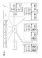
- FIG. 1is a diagram of a portion of an example communications and data management system in accordance with aspects of the present disclosure
- FIG. 2is a block diagram of one implementation of a communications management system that includes PLI functionality as well as PLM functionality in accordance with aspects of the present disclosure
- FIG. 3is a block diagram of one high-level example of a port and media reading interface that are suitable for use in the management system of FIG. 2 in accordance with aspects of the present disclosure
- FIG. 4is a perspective view of an example connector arrangement in the form of a modular RJ plug in accordance with the principles of the present disclosure
- FIG. 5is an exploded perspective view of the modular RJ plug of FIG. 5 in accordance with the principles of the present disclosure
- FIG. 6is a further exploded perspective view of the modular RJ plug of FIG. 5 in accordance with the principles of the present disclosure
- FIG. 7is a still further exploded perspective view of the modular RJ plug of FIG. 5 in accordance with the principles of the present disclosure
- FIG. 8is a perspective view of an example flexible circuit of the modular RJ plug of FIG. 5 in accordance with the principles of the present disclosure
- FIGS. 9-19show an example connector assembly in the form of a patch panel defining at least one socket, which can receive the connector arrangement for signal transmission in accordance with the principles of the present disclosure
- FIGS. 20-22show another example of a connector arrangement in the form of a modular plug for terminating an electrical communications cable in accordance with the principles of the present disclosure.
- FIGS. 23-38show an example connector assembly and components thereof in accordance with the principles of the present disclosure.
- FIG. 1is a diagram of a portion of an example communications and data management system 100 .
- the example system 100 shown in FIG. 1includes a part of a communications network 101 along which communications signals S 1 pass.
- the network 101can include an Internet Protocol network. In other implementations, however, the communications network 101 may include other types of networks.
- the communications network 101includes interconnected network components (e.g., connector assemblies, inter-networking devices, internet working devices, servers, outlets, and end user equipment (e.g., computers)).
- communications signals S 1pass from a computer to a wall outlet to a port of communication panel, to a first port of an inter-networking device, out another port of the inter-networking device, to a port of the same or another communications panel, to a rack mounted server.
- the portion of the communications network 101 shown in FIG. 1includes first and second connector assemblies 130 , 130 ′ at which communications signals S 1 pass from one portion of the communications network 101 to another portion of the communications network 101 .
- connector assemblies 130 , 130 ′include, for example, rack-mounted connector assemblies (e.g., patch panels, distribution units, and media converters for fiber and copper physical communication media), wall-mounted connector assemblies (e.g., boxes, jacks, outlets, and media converters for fiber and copper physical communication media), and inter-networking devices (e.g., switches, routers, hubs, repeaters, gateways, and access points).
- the first connector assembly 130defines at least one port 132 configured to communicatively couple at least a first media segment 105 to at least a second media segment 115 to enable the communication signals S 1 to pass between the media segments 105 , 115 .
- the at least one port 132 of the first connector assembly 130may be directly connected to a port 132 ′ of the second connector assembly 130 ′.
- the port 132is directly connected to the port 132 ′ when the communications signals S 1 pass between the two ports 132 , 132 ′ without passing through an intermediate port. For example, routing a patchcord between port 132 and port 132 ′ directly connects the ports 132 , 132 ′.
- the port 132 of the first connector assembly 130also may be indirectly connected to the port 132 ′ of the second connector assembly 130 ′.
- the port 132is indirectly connected to the port 132 ′ when the communications signals S 1 pass through an intermediate port when traveling between the ports 132 , 132 ′.
- the communications signals S 1may be routed over one media segment from the port 132 at the first connector assembly 130 to a port of a third connector assembly at which the media segment is coupled to another media segment that is routed from the port of the third connector assembly to the port 132 ′ of the second connector assembly 130 ′.
- Non-limiting examples of media segmentsinclude optical fibers, which carry optical data signals, and electrical conductors (e.g., CAT-5, 6, and 7 twisted-pair cables), which carry electrical data signals.
- Media segmentsalso can include electrical plugs, fiber optic connectors (e.g., SC, LC, FC, LX.5, or MPO connectors), adapters, media converters, and other physical components terminating to the fibers, conductors, or other such media segments.
- the techniques described herealso can be used with other types of connectors including, for example, BNC connectors, F connectors, DSX jacks and plugs, bantam jacks and plugs.
- each media segment 105 , 115is terminated at a plug or connector 110 , 120 , respectively, which is configured to communicatively connect the media segments 105 , 115 .
- the port 132 of the connector assembly 130can be configured to align ferrules of two fiber optic connectors 110 , 120 .
- the port 132 of the connector assembly 130can be configured to electrically connect an electrical plug with an electrical socket (e.g., a jack).
- the port 132can include a media converter configured to connect an optical fiber to an electrical conductor.
- the connector assembly 130does not actively manage (e.g., is passive with respect to) the communications signals S 1 passing through port 132 .
- the connector assembly 130does not modify the communications signal S 1 carried over the media segments 105 , 115 .
- the connector assembly 130does not read, store, or analyze the communications signal S 1 carried over the media segments 105 , 115 .
- the communications and data management system 100also provides physical layer information (PLI) functionality as well as physical layer management (PLM) functionality.
- PLI functionalityrefers to the ability of a physical component or system to identify or otherwise associate physical layer information with some or all of the physical components used to implement the physical layer of the system.
- PLM functionalityrefers to the ability of a component or system to manipulate or to enable others to manipulate the physical components used to implement the physical layer of the system (e.g., to track what is connected to each component, to trace connections that are made using the components, or to provide visual indications to a user at a selected component).
- physical layer informationrefers to information about the identity, attributes, and/or status of the physical components used to implement the physical layer of the communications system 101 .
- physical layer information of the communications system 101can include media information, device information, and location information.
- media informationrefers to physical layer information pertaining to cables, plugs, connectors, and other such media segments.
- the media informationis stored on or in the media segments, themselves.
- the media informationcan be stored at one or more data repositories for the communications system, either alternatively or in addition to the media, themselves.
- Non-limiting examples of media informationinclude a part number, a serial number, a plug or other connector type, a conductor or fiber type, a cable or fiber length, cable polarity, a cable or fiber pass-through capacity, a date of manufacture, a manufacturing lot number, information about one or more visual attributes of physical communication media (e.g., information about the color or shape of the physical communication media or an image of the physical communication media), and an insertion count (i.e., a record of the number of times the media segment has been connected to another media segment or network component).
- Media informationalso can include testing or media quality or performance information. The testing or media quality or performance information, for example, can be the results of testing that is performed when a particular segment of media is manufactured.
- device informationrefers to physical layer information pertaining to the communications panels, inter-networking devices, media converters, computers, servers, wall outlets, and other physical communications devices to which the media segments attach.
- the device informationis stored on or in the devices, themselves.
- the device informationcan be stored at one or more data repositories for the communications system, either alternatively or in addition to the devices, themselves.
- Non-limiting examples of device informationinclude a device identifier, a device type, port priority data (that associates a priority level with each port), and port updates (described in more detail herein).
- location informationrefers to physical layer information pertaining to a physical layout of a building or buildings in which the network 101 is deployed. Location information also can include information indicating where each communications device, media segment, network component, or other component that is physically located within the building. In accordance with some aspects, the location information of each system component is stored on or in the respective component. In accordance with other aspects, the location information can be stored at one or more data repositories for the communications system, either alternatively or in addition to the system components, themselves.
- one or more of the components of the communications network 101is configured to store physical layer information pertaining to the component as will be disclosed in more detail herein.
- the connectors 110 , 120 , the media segments 105 , 115 , and/or the connector assemblies 130 , 130 ′may store physical layer information.
- each connector 110 , 120may store information pertaining to itself (e.g., type of connector, data of manufacture, etc.) and/or to the respective media segment 105 , 115 (e.g., type of media, test results, etc.).
- the media segments 105 , 115 or connectors 110 , 120may store media information that includes a count of the number of times that the media segment (or connector) has been inserted into port 132 .
- the count stored in or on the media segmentis updated each time the segment (or plug or connector) is inserted into port 132 .
- This insertion count valuecan be used, for example, for warranty purposes (e.g., to determine if the connector has been inserted more than the number of times specified in the warranty) or for security purposes (e.g., to detect unauthorized insertions of the physical communication media).
- one or more of the components of the communications network 101also can read the physical layer information from one or more media segments retained thereat.
- one or more network componentsincludes a media reading interface that is configured to read physical layer information stored on or in the media segments or connectors attached thereto.
- the connector assembly 130includes a media reading interface 134 that can read media information stored on the media cables 105 , 115 retained within the port 132 .
- the media reading interface 134can read media information stored on the connectors or plugs 110 , 120 terminating the cables 105 , 115 , respectively.
- some types of physical layer informationcan be obtained by the connector assembly 130 from a user at the connector assembly 130 via a user interface (e.g., a keypad, a scanner, a touch screen, buttons, etc.).
- the connector assembly 130can provide the physical layer information obtained from the user to other devices or systems that are coupled to the network 101 (as described in more detail herein).
- some or all physical layer informationcan be obtained by the connector assembly 130 from other devices or systems that are coupled to the network 101 .
- physical layer information pertaining to media that is not configured to store such informationcan be entered manually into another device or system that is coupled to the network 101 (e.g., at the connector assembly 130 , at the computer 160 , or at the aggregation point 150 ).
- some types of non-physical layer informationcan be obtained by one network component from other devices or systems that are coupled to the network 101 .
- the connector assembly 130may pull non-physical layer information from one or more components of the network 101 .
- the non-physical layer informationcan be obtained by the connector assembly 130 from a user at the connector assembly 130 .
- the physical layer information read by a network componentmay be processed or stored at the component.
- the first connector assembly 130 shown in FIG. 1is configured to read physical layer information stored on the connectors 110 , 120 and/or on the media segments 105 , 115 using media reading interface 134 .
- the first connector assembly 130may store not only physical layer information about itself (e.g., the total number of available ports at that assembly 130 , the number of ports currently in use, etc.), but also physical layer information about the connectors 110 , 120 inserted at the ports and/or about the media segments 105 , 115 attached to the connectors 110 , 120 .
- the connector assembly 130is configured to add, delete, and/or change the physical layer information stored in or on the segment of physical communication media 105 , 115 (i.e., or the associated connectors 110 , 120 ).
- the media information stored in or on the segment of physical communication media 105 , 115can be updated to include the results of testing that is performed when a segment of physical media is installed or otherwise checked.
- such testing informationis supplied to the aggregation point 150 for storage and/or processing.
- modification of the physical layer informationdoes not affect the communications signals S 1 passing through the connector assembly 130 .
- the physical layer information obtained by the media reading interfacemay be communicated (see PLI signals S 2 ) over the network 101 for processing and/or storage.
- the components of the communications network 101are connected to one or more aggregation devices 150 (described in greater detail herein) and/or to one or more computing systems 160 .
- each connector assembly 130includes a PLI port 136 that is separate from the “normal” ports 132 of the connector assembly 130 .
- Physical layer informationis communicated between the connector assembly 130 and the network 101 through the PLI port 136 .
- the connector assembly 130is connected to a representative aggregation device 150 , a representative computing system 160 , and to other components of the network 101 (see looped arrow) via the PLI port 136 .
- the physical layer informationis communicated over the network 101 just like any other data that is communicated over the network 101 , while at the same time not affecting the communication signals S 1 that pass through the connector assembly 130 on the normal ports 132 .
- the physical layer informationmay be communicated as one or more of the communication signals S 1 that pass through the normal ports 132 of the connector assemblies 130 , 130 ′.
- a media segmentmay be routed between the PLI port 136 and one of the “normal” ports 132 .
- the physical layer informationmay be passed along the communications network 101 to other components of the communications network 101 (e.g., to the one or more aggregation points 150 and/or to the one or more computer systems 160 ).
- the communications network 101includes a data network along which the physical layer information described above is communicated. At least some of the media segments and other components of the data network may be separate from those of the communications network 101 to which such physical layer information pertains.
- the first connector assembly 130may include a plurality of fiber optic adapters defining ports at which connectorized optical fibers are optically coupled together to create an optical path for communications signals S 1 .
- the first connector assembly 130also may include one or more electrical cable ports at which the physical layer information (see PLI signals S 2 ) are passed to other parts of the data network. (e.g., to the one or more aggregation points 150 and/or to the one or more computer systems 160 ).
- FIG. 2is a block diagram of one example implementation of a communications management system 200 that includes PLI functionality as well as PLM functionality.
- the management system 200comprises a plurality of connector assemblies 202 .
- the system 200includes one or more connector assemblies 202 connected to an IP network 218 .
- the connector assemblies 202 shown in FIG. 2illustrate various implementations of the connector assembly 130 of FIG. 1 .
- Each connector assembly 202includes one or more ports 204 , each of which is used to connect two or more segments of physical communication media to one another (e.g., to implement a portion of a logical communication link for communication signals S 1 of FIG. 1 ). At least some of the connector assemblies 202 are designed for use with segments of physical communication media that have physical layer information stored in or on them. The physical layer information is stored in or on the segment of physical communication media in a manner that enables the stored information, when the segment is attached to a port 204 , to be read by a programmable processor 206 associated with the connector assembly 202 .
- each of the ports 204 of the connector assemblies 202comprises a respective media reading interface 208 via which the respective programmable processor 206 is able to determine if a physical communication media segment is attached to that port 204 and, if one is, to read the physical layer information stored in or on the attached segment (if such media information is stored therein or thereon).
- the programmable processor 206 associated with each connector assembly 202is communicatively coupled to each of the media reading interfaces 208 using a suitable bus or other interconnect (not shown).
- each connector assembly 202includes its own respective programmable processor 206 and its own respective network interface 216 that is used to communicatively couple that connector assembly 202 to an Internet Protocol (IP) network 218 .
- IPInternet Protocol
- a group of connector assemblies 202are physically located near each other (e.g., in a bay or equipment closet). Each of the connector assemblies 202 in the group includes its own respective programmable processor 206 . However, in the second connector assembly configuration 212 , some of the connector assemblies 202 (referred to here as “interfaced connector assemblies”) include their own respective network interfaces 216 while some of the connector assemblies 202 (referred to here as “non-interfaced connector assemblies”) do not. The non-interfaced connector assemblies 202 are communicatively coupled to one or more of the interfaced connector assemblies 202 in the group via local connections.
- the non-interfaced connector assemblies 202are communicatively coupled to the IP network 218 via the network interface 216 included in one or more of the interfaced connector assemblies 202 in the group.
- the total number of network interfaces 216 used to couple the connector assemblies 202 to the IP network 218can be reduced.
- the non-interfaced connector assemblies 202are connected to the interfaced connector assembly 202 using a daisy chain topology (though other topologies can be used in other implementations and embodiments).
- a group of connector assemblies 202are physically located near each other (e.g., within a bay or equipment closet). Some of the connector assemblies 202 in the group (also referred to here as “master” connector assemblies 202 ) include both their own programmable processors 206 and network interfaces 216 , while some of the connector assemblies 202 (also referred to here as “slave” connector assemblies 202 ) do not include their own programmable processors 206 or network interfaces 216 . Each of the slave connector assemblies 202 is communicatively coupled to one or more of the master connector assemblies 202 in the group via one or more local connections.
- the programmable processor 206 in each of the master connector assemblies 202is able to carry out the PLM functions for both the master connector assembly 202 of which it is a part and any slave connector assemblies 202 to which the master connector assembly 202 is connected via the local connections. As a result, the cost associated with the slave connector assemblies 202 can be reduced.
- the slave connector assemblies 202are connected to a master connector assembly 202 in a star topology (though other topologies can be used in other implementations and embodiments).
- Each programmable processor 206is configured to execute software or firmware that causes the programmable processor 206 to carry out various functions described below.
- Each programmable processor 206also includes suitable memory (not shown) that is coupled to the programmable processor 206 for storing program instructions and data.
- the programmable processor 206determines if a physical communication media segment is attached to a port 204 with which that processor 206 is associated and, if one is, to read the identifier and attribute information stored in or on the attached physical communication media segment (if the segment includes such information stored therein or thereon) using the associated media reading interface 208 .
- a group of connector assemblies 202are housed within a common chassis or other enclosure.
- Each of the connector assemblies 202 in the configuration 215includes their own programmable processors 206 .
- the programmable processors 206 in each of the connector assembliesare “slave” processors 206 .
- Each of the slave programmable processor 206is also communicatively coupled to a common “master” programmable processor 217 (e.g., over a backplane included in the chassis or enclosure).
- the master programmable processor 217is coupled to a network interface 216 that is used to communicatively couple the master programmable processor 217 to the IP network 218 .
- each slave programmable processor 206is configured to determine if physical communication media segments are attached to its port 204 and to read the physical layer information stored in or on the attached physical communication media segments (if the attached segments have such information stored therein or thereon) using the associated media reading interfaces 208 .
- the physical layer informationis communicated from the slave programmable processor 206 in each of the connector assemblies 202 in the chassis to the master processor 217 .
- the master processor 217is configured to handle the processing associated with communicating the physical layer information read from by the slave processors 206 to devices that are coupled to the IP network 218 .
- the system 200includes functionality that enables the physical layer information that the connector assemblies 202 capture to be used by application-layer functionality outside of the traditional physical-layer management application domain. That is, the physical layer information is not retained in a PLM “island” used only for PLM purposes but is instead made available to other applications.
- the management system 200includes an aggregation point 220 that is communicatively coupled to the connector assemblies 202 via the IP network 218 .
- the aggregation point 220includes functionality that obtains physical layer information from the connector assemblies 202 (and other devices) and stores the physical layer information in a data store.
- the aggregation point 220can be used to receive physical layer information from various types of connector assemblies 202 that have functionality for automatically reading information stored in or on the segment of physical communication media.
- the aggregation point 220 and aggregation functionality 224can be used to receive physical layer information from other types of devices that have functionality for automatically reading information stored in or on the segment of physical communication media. Examples of such devices include end-user devices—such as computers, peripherals (e.g., printers, copiers, storage devices, and scanners), and IP telephones—that include functionality for automatically reading information stored in or on the segment of physical communication media.
- the aggregation point 220also can be used to obtain other types of physical layer information.
- the aggregation point 220also obtains information about physical communication media segments that is not otherwise automatically communicated to an aggregation point 220 .
- This informationcan be provided to the aggregation point 220 , for example, by manually entering such information into a file (e.g., a spreadsheet) and then uploading the file to the aggregation point 220 (e.g., using a web browser) in connection with the initial installation of each of the various items.
- a filee.g., a spreadsheet
- Such informationcan also, for example, be directly entered using a user interface provided by the aggregation point 220 (e.g., using a web browser).
- the aggregation point 220also includes functionality that provides an interface for external devices or entities to access the physical layer information maintained by the aggregation point 220 . This access can include retrieving information from the aggregation point 220 as well as supplying information to the aggregation point 220 .
- the aggregation point 220is implemented as “middleware” that is able to provide such external devices and entities with transparent and convenient access to the PLI maintained by the access point 220 .
- the aggregation point 220aggregates PLI from the relevant devices on the IP network 218 and provides external devices and entities with access to such PLI, the external devices and entities do not need to individually interact with all of the devices in the IP network 218 that provide PLI, nor do such devices need to have the capacity to respond to requests from such external devices and entities.
- a network management system (NMS) 230includes PLI functionality 232 that is configured to retrieve physical layer information from the aggregation point 220 and provide it to the other parts of the NMS 230 for use thereby.
- the NMS 230uses the retrieved physical layer information to perform one or more network management functions.
- the NMS 230communicates with the aggregation point 220 over the IP network 218 .
- an application 234 executing on a computer 236can also use the API implemented by the aggregation point 220 to access the PLI information maintained by the aggregation point 220 (e.g., to retrieve such information from the aggregation point 220 and/or to supply such information to the aggregation point 220 ).
- the computer 236is coupled to the IP network 218 and accesses the aggregation point 220 over the IP network 218 .
- one or more inter-networking devices 238 used to implement the IP network 218include physical layer information (PLI) functionality 240 .
- the PLI functionality 240 of the inter-networking device 238is configured to retrieve physical layer information from the aggregation point 220 and use the retrieved physical layer information to perform one or more inter-networking functions.
- Examples of inter-networking functionsinclude Layer 1, Layer 2, and Layer 3 (of the OSI model) inter-networking functions such as the routing, switching, repeating, bridging, and grooming of communication traffic that is received at the inter-networking device.
- the aggregation point 220can be implemented on a standalone network node (e.g., a standalone computer running appropriate software) or can be integrated along with other network functionality (e.g., integrated with an element management system or network management system or other network server or network element). Moreover, the functionality of the aggregation point 220 can be distribute across many nodes and devices in the network and/or implemented, for example, in a hierarchical manner (e.g., with many levels of aggregation points).
- the IP network 218can include one or more local area networks and/or wide area networks (e.g., the Internet). As a result, the aggregation point 220 , NMS 230 , and computer 236 need not be located at the same site as each other or at the same site as the connector assemblies 202 or the inter-networking devices 238 .
- powercan be supplied to the connector assemblies 202 using conventional “Power over Ethernet” techniques specified in the IEEE 802.3af standard, which is hereby incorporated herein by reference.
- a power hub 242 or other power supplying devicelocated near or incorporated into an inter-networking device that is coupled to each connector assembly 202 ) injects DC power onto one or more of the wires (also referred to here as the “power wires”) included in the copper twisted-pair cable used to connect each connector assembly 202 to the associated inter-networking device.
- FIG. 3is a schematic diagram of one example connection system 300 including a connector assembly 320 configured to collect physical layer information from a connector arrangement 310 .
- the example connection system 300 shownincludes a jack module 320 and an electrical plug 310 .
- the connector arrangement 310terminates at least a first electrical segment (e.g., a conductor cable) 305 of physical communications media and the connector assembly 320 terminates at least second electrical segments (e.g., twisted pairs of copper wires) 329 of physical communications media.
- the connector assembly 320defines at least one socket port 325 in which the connector arrangement 310 can be accommodated.
- Each electrical segment 305 of the connector arrangement 310carries communication signals (e.g., communications signals S 1 of FIG. 1 ) to primary contact members 312 on the connector arrangement 310 .
- the connector assembly 320includes a primary contact arrangement 322 that is accessible from the socket port 325 .
- the primary contact arrangement 322is aligned with and configured to interface with the primary contact members 312 to receive the communications signals (S 1 of FIG. 1 ) from the primary contact members 312 when the connector arrangement 310 is inserted into the socket 325 of the connector assembly 320 .
- the connector assembly 320is electrically coupled to one or more printed circuit boards.
- the connector assembly 320can support or enclose a first printed circuit board 326 , which connects to insulation displacement contacts (IDCs) 327 or to another type of electrical contacts.
- IDCsinsulation displacement contacts
- the IDCs 327terminate the electrical segments 329 of physical communications media (e.g., conductive wires).
- the first printed circuit board 326manages the primary communication signals carried from the conductors terminating the cable 305 to the electrical segments 329 that couple to the IDCs 327 .
- the connector arrangement 310can include a storage device 315 configured to store physical layer information.
- the connector arrangement 310also includes second contact members 314 that are electrically coupled (i.e., or otherwise communicatively coupled) to the storage device 315 .
- the storage device 315is implemented using an EEPROM (e.g., a PCB surface-mount EEPROM).
- the storage device 315is implemented using other non-volatile memory device. Each storage device 315 is arranged and configured so that it does not interfere or interact with the communications signals communicated over the media segment 305 .
- the connector assembly 320also includes a second contact arrangement (e.g., a media reading interface) 324 .
- the media reading interface 324is accessible through the socket port 325 .
- the second contact arrangement 324is aligned with and configured to interface with the second contact members 314 of the media segment to receive the physical layer information from the storage device 315 when the connector arrangement 310 is inserted into the socket 325 of the connector assembly 320 .
- the storage device interfaces 314 and the media reading interfaces 324each comprise three (3) leads—a power lead, a ground lead, and a data lead.
- the three leads of the storage device interface 314come into electrical contact with three (3) corresponding leads of the media reading interface 324 when the corresponding media segment is inserted in the corresponding port 325 .
- a two-line interfaceis used with a simple charge pump.
- additional leadscan be provided (e.g., for potential future applications).
- the storage device interfaces 314 and the media reading interfaces 324may each include four (4) leads, five (5) leads, six (6) leads, etc.
- the storage device 315also may include a processor or micro-controller, in addition to the storage for the physical layer information.
- the micro-controllercan be used to execute software or firmware that, for example, performs an integrity test on the cable 305 (e.g., by performing a capacitance or impedance test on the sheathing or insulator that surrounds the cable 305 , (which may include a metallic foil or metallic filler for such purposes)).
- the micro-controllercan communicate that fact to a programmable processor (e.g., processor 206 of FIG. 2 ) associated with the port using the storage device interface (e.g., by raising an interrupt).
- the micro-controlleralso can be used for other functions.
- the connector assembly 320also can support or enclose a second printed circuit board 328 , which connects to the second contact arrangement 324 .
- the second printed circuit board 328manages the physical layer information communicated from a storage device 315 through second contacts 314 , 324 .
- the second printed circuit board 328is positioned on an opposite side of the connector assembly 320 from the first printed circuit board 326 .
- the printed circuit boards 326 , 328can be positioned on the same side or on different sides.
- the second printed circuit board 328is positioned horizontally relative to the connector assembly 320 (see FIG. 3 ).
- the second printed circuit board 328is positioned vertically relative to the connector assembly 320 .
- the second printed circuit board 328can be communicatively connected to one or more programmable electronic processors and/or one or more network interfaces.
- one or more such processors and interfacescan be arranged as components on the printed circuit board 328 .
- one of more such processor and interfacescan be arranged on a separate circuit board that is coupled to the second printed circuit board 328 .
- the second printed circuit board 328can couple to other circuit boards via a card edge type connection, a connector-to-connector type connection, a cable connection, etc.
- the network interfaceis configured to send the physical layer information to the data network (e.g., see signals S 2 of FIG. 1 ).
- FIGS. 4-19provide an example implementation of physical layer management networks and components for electrical (e.g., copper) communications applications.
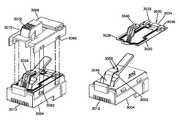
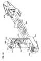
- FIGS. 4-8show an example of a connector arrangement 3000 in the form of a modular plug 3002 for terminating an electrical communications cable.
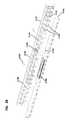
- FIGS. 9-19show an example connector assembly 3100 in the form of a patch panel 3102 defining at least one socket 3106 , which can receive the connector arrangement 3000 for signal transmission.
- the connector arrangement 3000includes an RJ plug 3002 that connects to the end of an electrical segment of communications media, such as twisted pair copper cable.
- the socket 3106 of the connector assembly 3100defines an RJ jack (e.g., an RJ-45 jack).
- the RJ plug 3002is insertable into a port of a mating RJ jack 3106 in the patch panel 3102 of the connector assembly 3100 as will be described below.
- the connector arrangement 3000 and connector assembly 3100can define other types of electrical connections.
- the plug 3002includes a plug nose body 3004 for holding main signal contacts 3012 , which are electrically connected to segments of communications media terminated at the plug 3002 .
- the main contacts 3012may be connected to twisted pair conductors of a communications cable.
- the main signal contacts 3012are arranged at a front end 3014 of the plug 3002 .
- the main signal contacts 3012are positioned to electrically connect to contacts positioned in the jack 3106 for signal transmission.
- the plug 3002further includes a finger tab 3050 , which facilitates latching the connector arrangement 3000 to the connector assembly 3100 .
- the finger tab 3050includes a latch surface 3052 for latching to the connector assembly 3100 .
- the finger tab 3050extends from the plug nose body 3004 .
- plugs 3002also include a keying structure 3015 that is shaped to mate with a keyway 3065 defined in the connector assembly 3100 .
- the keying structure 3015is formed at a base of the finger tab 3050 .
- Certain types of plugs 3002also include wire managers 3008 for managing the electrical segments of communications media (e.g., twisted wire pairs) and a strain relief boot 3010 which snaps to the plug nose body 3004 .
- the plug 3002also includes a plug cover 3006 that mounts on the plug nose body 3004 (see FIGS. 4-6 ).
- the plug cover 3006defines side opening 3066 for receiving the side tabs 3062 defined on the plug nose body 3004 .
- Certain types of plug covers 3006mount over the finger tab 3050 .
- the plug cover 3006may defines a cavity, slot, or recess for receiving the finger tab 3050 .
- the connector arrangement 3000also includes a storage device 3030 ( FIGS. 6 and 7 ) that is configured to store physical layer information (e.g., an identifier and/or attribute information) pertaining to the segment of physical communications media (e.g., the plug 3002 and/or the electrical cable terminated thereby).
- the storage device 3030is electrically connected to one or more second contacts 3026 .
- Certain types of connector arrangements 3000also can include additional components to aid in physical layer management.
- FIG. 7is an exploded view of a plug component 3003 including the storage device 3030 and plug nose body 3004 .
- the second contacts 3026are located within the keying structure 3015 .
- the keying structure 3015defines slotted openings (e.g., see slotted openings 3072 of FIG. 4 ) providing access to the second contacts 3026 (see FIG. 6 ).
- the plug cover 3006defines the slotted openings 3072 for contacts 3026 to be exposed for contact with mating contacts of a media reading interface 3188 of the connector assembly 3100 .
- the connector arrangement 3000also can include a communications device 3036 that is configured to send and receive communications signals to and from a local source.
- the communications device 3036can include an IR transceiver.
- Such a communications device 3036can enable a technician to read and/or write data to the storage device 3030 using an infra-red wand or probe (e.g., a handheld wand or probe). Accordingly, the technician can access information stored on the connector arrangement 3000 without plugging the connector arrangement 3000 into a port of connector assembly 3100 .
- the storage device 3030can be arranged on a circuit 3020 ( FIG. 8 ) that is mounted to the modular plug 3002 (see FIGS. 7-8 ).
- the circuit 3020is positioned between plug nose body 3004 and plug cover 3006 .
- at least a portion of the circuit 3020is located within the keying structure 3015 .
- additional componentssuch as the communications device 3036 , can be arranged on the circuit 3020 .
- the circuit 3020includes a substrate 3022 with conductive traces 3024 connecting lands 3028 to the second contacts 3026 (e.g., see FIGS. 6-8 ).
- the circuit 3020also includes circuit components, including the media storage device 3030 , installed at the lands 3028 .
- the storage device 3030may be accessed via the second contacts 3026 .
- the storage device 3030includes an electrically erasable programmable read-only memory (EEPROM) 3034 .
- EEPROMelectrically erasable programmable read-only memory
- the storage device 3030can include any suitable type of memory.
- the circuit componentsalso may include a metal-oxide-semiconductor field-effect transistor (MOSFET) 3032 .
- MOSFETmetal-oxide-semiconductor field-effect transistor
- the circuit 3020is a flexible circuit that defines a base portion 3038 and an extending portion 3040 .
- the MOSFET 3032 , the EEPROM 3034 , and the IR device 3036can be mounted to the base portion 3038 .
- the circuit contacts 3026can be arranged on the extending portion 3040 .
- the extending portion 3040is located within the keying structure 3015 .
- the extending portion 3040is located on the finger tab 3050 .
- the circuit contacts 3026permit connection of the EEPROM 3034 to a media reading interface 3188 of the connector assembly 3100 as will be disclosed herein.
- the flexible circuit 3020is positioned along an outer surface 3042 of plug nose body 3004 .
- the extending portionis positioned on the same side of the plug as the finger tab 3050 .
- the base portion 3038 of the flexible circuit 3020is positioned along a periphery of surface 3042 .
- Extending portion 3040is positioned over a flexible rib 3046 of plug nose body 3004 .
- Rib 3046supports flexible circuit 3020 in the area of extending portion 3040 so that contacts 3026 are positioned to engage the media reading interface 3188 associated with the connector assembly 3100 .
- Rib 3046includes retainer pegs 3058 for engaging holes 3060 on extending portion 3040 of the flexible circuit 3020 for retention.
- Connector assembly 3100forms a patch panel 3102 for rack or frame mounting and defines a plurality of ports 3104 .
- Connector assembly 3100includes a plurality of modular RJ jack modules (e.g., RJ 45 jack modules) 3106 which snap-fit to connector assembly 3100 to define the ports 3104 .
- RJ jack modules 3106connect to twisted pair cables, or other signal transmission structures, such as PCBs.
- a front opening 3110 of each jack module 3106receives the front end 3014 ( FIG. 4 ) of the plug 3002 to enable main signal transmission from the cable through jack module 3106 to another cable or other signal transmission media.
- Certain types of jack modules 3106are configured to latchingly receive the finger tab 3050 to secure the plug 3002 to the jack module 3106 .
- the connector assembly 3100also includes a media reading interface 3188 ( FIGS. 11 and 17 ) that permits reading (e.g., by a processor) of the information stored in the storage device 3030 of the connector arrangement 3000 .
- the information read from the storage device 3030can be transferred to a physical layer management network (e.g., network 101 of FIG. 1 , network 218 of FIG. 2 , etc.).
- a physical layer management networke.g., network 101 of FIG. 1 , network 218 of FIG. 2 , etc.
- the circuitry associated with storage device 3030 and the circuitry associated with media reading interface 3188does not affect the main signal interface between the plug and the jack.
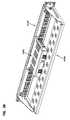
- the patch panel 3102includes circuitry 3180 ( FIG. 9 ) mounted to a frame 3120 and a front panel or fascia 3160 (see FIG. 10 ).
- the circuitry 3180is enclosed between the frame 3120 and the fascia 3160 .
- Certain types of circuitry 3180include a main PCB 3182 ( FIG. 9 ).
- the main PCB 3182is mounted to the fascia 3160 , which is mounted to the frame 3120 .
- the main PCB 3182defines openings 3183 that align with ports of the jack modules 306 . Each opening is configured to enable passage of a modular plug 3002 through the PCB 3182 and into one of the modular jacks 3106 (e.g., see FIGS. 17-18 ).
- the main PCB 3182includes a main communications interface connector 3184 and jack interface connectors 3186 (see FIGS. 11-12 ).
- Jack interface connectors 3186form the media reading interface 3188 for connector assembly 3100 .
- the jack interface connectors 3186include a contact set 3190 having a body 3192 and projections 3194 for connecting to the main PCB 3182 through holes 3218 defined in the PCB 3182 .
- Contact set 3190includes a plurality of conductive contacts 3198 .
- PLM functionalitycan be retrofitted to existing systems.
- conventional jack modulescan be snap-fitted into a frame 3120 coupled to a main PCB 3182 as described above.
- the main PCB 3182also defines holes 3210 ( FIG. 9 ) for heat staking main PCB 3182 to front panel 3160 (e.g., see FIG. 12 ). Locator holes 3212 align with posts 3166 of front panel 3160 to facilitate assembly of the PCB 3182 to front panel 3160 (see FIG. 11 ).
- the circuitry 3180includes an LED indicator 3216 adjacent each opening 3183 of the PCB 3182 .
- each LED indicator 3216is a bi-color indicator.
- a microswitch 3124FIG. 17
- the frame 3120includes a main portion 3122 and ends 3124 , 3126 . Each end 3124 , 3126 of the frame 3120 includes holes 3128 to mount frame 3120 to a rack.
- the main portion 3122 of the frame 3120includes upper and lower flanges 3140 . Tabs 3142 on the flanges 3140 cooperate with a complementary mating structure on the fascia 3160 to connect the fascia 3160 to the frame 3120 (see FIG. 13 ).
- Standoffs 3144accept screws 3145 or other fasteners for mounting the front panel 3160 to the frame 3120 .
- the main portion 3122 of the frame 3120defines one or more openings 3132 configured to receive the jack modules 3106 .
- Frame 3120also defines a second aperture 3134 ( FIG. 10 ) configured to receive the communications interface connector 3184 (e.g., see FIG. 15 ).
- the front panel 3160defines openings 3162 that align with openings 3110 of the jack modules 3106 when the jack modules 3106 are mounted to the frame 3120 . Plugs 3002 of the connector arrangement 3000 can be inserted through the openings 3162 and into the jacks 3106 .
- the front panel 3160also defines openings 3164 for the passage of light signals from the LED indicators 3216 of the internal circuitry 3180 .
- each opening 3162 of the front panel 3160defines a keyway 3165 shaped to receive the keying structure 3015 of the connector arrangement 3000 .
- each opening 3162defines a recessed keyway 3165 extending downwardly.
- the finger tabs 3050 of certain types of connector arrangements 3000are configured to latch in the keyway 3165 .
- the opening 3162 and keyway 3165are generally T-shaped (e.g., see FIG. 10 ).
- the media reading interfaces 3188align with the openings 3162 of the front panel 3160 .
- the media reading interfaces 3188are positioned adjacent the keyways 3165 (e.g., see FIG. 12 ).
- each media reading interface 3188can be positioned beneath one of the keyways 3165 at the front panel openings 3162 .
- second contacts 3026 located within the keying structure 3015 of the connector arrangement 3000interface with the media reading interface 3188 when the connector arrangement 3000 is inserted through the opening 3162 of the front panel 3160 and into the jack module 3110 .
- contacts of the media reading interface 3188may extend through the slots 3072 of the connector arrangement 3000 .
- FIG. 19shows an example connector arrangement 3000 being inserted into an example connector assembly 3100 .
- informationis read from media storage device 3030 of the connector arrangement 3000 by a CPU card 3300 connected to main communications interface connector 3184 (see FIG. 16 ).
- the CPU card 3300includes circuitry and components including a processor that is configured to read information obtained from the storage device 3030 of the connector arrangement 3000 .
- Communications ports 3302 , 3304 of the CPU card 3300can be connected to the physical layer management network.
- a power port 3306also can be defined by the CPU card 3300 .
- FIGS. 20-38provide another example implementation of physical layer management networks and components for electrical (e.g., copper) communications applications.
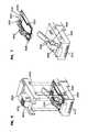
- FIGS. 20-22show another example of a connector arrangement 4000 in the form of a modular plug 4002 for terminating an electrical communications cable (not shown).
- FIGS. 23-38show an example connector assembly 4100 and components thereof.
- the connector assembly 4100is in the form of a patch panel 4102 defining at least one socket 4106 , which can receive the connector arrangement 4000 for signal transmission.
- the connector arrangement 4000includes an RJ plug 4002 that connects to the end of an electrical segment of communications media, such as twisted pair copper cable (not shown).
- the RJ plug 4002is insertable into a port of a mating RJ jack (e.g., an RJ-45 jack) 4106 in the patch panel 4102 of the connector assembly 4100 as will be described below (see FIG. 38 ).
- the connector arrangement 4000 and connector assembly 4100can define other types of electrical connections.
- the plug 4002includes a plug nose body 4004 ( FIG. 22 ) for holding main signal contacts 4012 , which are electrically connected to the twisted pair conductors of the communications cable.
- the main signal contacts 4012are arranged at a front end 4014 of the plug 4002 .
- the main signal contacts 4012electrically connect to contacts positioned in the jack module 4106 for signal transmission.
- the plug nose body 4004further includes a finger tab 4050 , which facilitates latching the connector arrangement 4000 to the connector assembly 4100 .
- the finger tab 4050includes a latch surface 4052 for latching to the connector assembly 4100 .
- the plug 4002also includes a plug cover 4006 that mounts on the plug nose body 4004 (see FIG. 22 ).
- the plug cover 4006mounts to an opposite side of the plug nose body 4004 from which the finger tab 4050 extends.
- the plug cover 4006defines latch arms 4007 configured to be received in openings 4003 defined in the plug nose body 4004 .
- the plug cover 4006also defines a plurality of slotted openings 4009 for circuit contacts to be exposed for contact with mating contacts 4190 of the media reading interface 4188 of the connector assembly 4100 .
- the plug cover 4006defines two sets of slotted openings 4009 .
- a platform 4005extends between the two sets of slotted openings 4009 .
- the plug 4002also includes a wire manager 4008 for managing the twisted wire pairs and a strain relief boot 4010 , which snaps to the plug nose body 4004 (see FIG. 22 ).
- the connector arrangement 4000also includes a storage device 4030 ( FIG. 22 ) that is configured to store information (e.g., an identifier and/or attribute information) pertaining to the segment of physical communications media (e.g., the plug 4002 and/or the electrical cable terminated thereat).
- the connector arrangement 4000also can include additional components to aid in physical layer management.
- the connector arrangement 4000also can include a communications device (not shown) that is configured to send and receive communications signals to and from a local source.
- the communications devicecan include an IR transceiver.
- Such a communications devicecan enable a technician to read and/or write data to the storage device 4030 using an infra-red wand or probe (e.g., a handheld wand or probe). Accordingly, the technician can access information stored on the connector arrangement 4000 without unplugging the connector arrangement 4000 from a port of connector assembly 4100 .
- the storage device 4030can be arranged on a circuit 4020 ( FIG. 22 ) that is mounted to the modular plug 4002 (see FIG. 22 ).
- the circuit 4020is positioned between plug nose body 4004 and plug cover 4006 .
- additional componentssuch as a MOSFET or a communications device, can be arranged on the circuit 4020 .
- the circuit 4020includes a substrate with conductive traces electrically connecting contacts and lands.
- the circuit 4020also includes circuit components, including the media storage device 4030 , at the lands.
- the circuit 4020includes a MOSFET 4032 , an EEPROM 4034 .
- the EEPROM 4034forms the media storage device 4030 for modular plug 4002 .
- the storage device 4030can include any suitable type of memory.
- the circuit 4020is an FR-4 PCB 4022 defining a U-shaped body having a base 4024 and legs 4026 .
- the MOSFET 4032 and the EEPROM 4034can be mounted to the base 4024 of the PCB 4022 .
- the circuit contactsare arranged on the legs 4026 of the PCB 4022 .
- the circuit contactspermit connection of the EEPROM 4034 to a media reading interface 4188 of the connector assembly 4100 as will be disclosed herein.
- contacts of the media reading interface 4188can extend through the slotted openings 4009 to connect to the circuit contacts.
- connector assembly 4100forms a patch panel 4102 for rack or frame mounting and defines a plurality of ports 4104 (see FIG. 31 ).
- connector assembly 4100includes one or more modular RJ 45 jack modules 4106 , which snap-fit to connector assembly 4100 to define the ports 4104 (see FIG. 38 ).
- the RJ jack modules 4106connect to twisted pair cables, or other signal transmission structures, such as PCBs. Plugs 4002 are inserted into jack modules 4106 to enable main signal transmission from the cable through jack module 4106 to another cable or other signal transmission media.
- the connector assembly 4100also includes a media reading interface 4188 ( FIG. 25 ) that permits reading (e.g., by a processor) of the information stored in the storage device 4030 of the connector arrangement 4000 .
- the information read from the storage device 4030can be transferred to a physical layer management network (e.g., network 101 of FIG. 1 , network 218 of FIG. 2 , etc.) as will be disclosed herein.
- a physical layer management networke.g., network 101 of FIG. 1 , network 218 of FIG. 2 , etc.
- the circuitry associated with storage device 4030 and the circuitry associated with media reading interface 4188does not affect the main signal transmission interface between the plug and the jack.
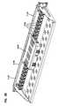
- the patch panel 4102includes internal circuitry 4180 ( FIGS. 23-24 ) enclosed between a frame 4120 ( FIGS. 28-30 ) and a fascia 4160 (see FIG. 31 ).
- Circuitry 4180includes a main PCB 4182 ( FIG. 23 ).
- the main PCB 4182includes a main communications interface connector 4184 and storage interface connectors 4186 (see FIGS. 11-12 ).
- the communications interface connector 4184is mounted to an upper end of the main PCB 4182 and the storage interface connectors 4186 are mounted to a lower end of the PCB 4182 .
- Storage interface connectors 4186form the media reading interface 4188 for connector assembly 4100 .
- the storage interface connectors 4186include a set of contacts 4190 that extend over a bottom edge of the PCB 4182 .
- a modular plug 4002can be arranged within the connector assembly 4100 so that the circuit contacts on the plug PCB 4022 contact the contacts 4190 on the PCB 4182 .
- the contacts 4190are split into two spaced groups.
- a microswitch 4224can be mounted to the PCB 4182 adjacent to each storage interface connector 4182 for sensing the presence of a connector arrangement 4000 inserted into the corresponding jack 4106 .
- the microswitch 4224extends downwardly from the PCB 4182 between the two groups of contacts 4190 (see FIG. 25 ).
- the microswitch 4224is depressed by the base 4005 of the plug 4002 .
- the PCB 4182also includes an LED indicator 4216 adjacent each storage interface connector 4186 of the PCB 4182 (see FIG. 25 ).
- each LED indicator 4216is a bi-color indicator.
- the indicator 4216can be used to indicate a particular jack module 4106 to a technician.
- the indicator 4216can be lit to indicate into which jack module 4106 a technician should insert a plug 4002 .
- the indicator 4216also can indicate which jack module 4106 contains a particular plug 4002 .
- the frame 4120includes a main portion 4122 and ends 4124 , 4126 . Each end 4124 , 4126 of the frame 4120 defines holes 4128 to mount frame 4120 to a rack.
- the main portion 4122 of the frame 4120includes upper and lower flanges 4140 .
- the main portion 4122defines one or more openings 4132 configured to receive the jack modules 4106 .
- Frame 4120also defines a second aperture 4134 ( FIG. 28 ) configured to receive the communications interface connector 4184 (e.g., see FIG. 33 ).
- the fascia 4160is coupled to the frame 4120 to secure the PCB 4182 therebetween.
- the fascia 4160defines opening 4162 ( FIG. 31 ) that align with openings 4110 of the jack modules 4106 when the jack modules 4106 are mounted to the frame 4120 .
- the PCB 4182is arranged above the openings 4162 . Plugs 4002 of the connector arrangement 4000 can be inserted through the openings 4162 and into the jack modules 4106 .
- the fascia 4160also defines openings 4164 for the passage of light signals from the LED indicators 4216 of the internal circuitry 4180 (see FIG. 31 ).
- the fascia 4160can be formed in multiple pieces.
- the fascia 4160includes an upper piece 4161 and a lower portion 4171 .
- the upper and lower pieces 4161 , 4171cooperate to define openings 4162 .
- the upper piece 4161includes legs 4166 extending downwardly from a main portion 4165 to define slots 4167 ( FIG. 26 ).
- the lower piece 4171includes flanges 4172 that extend upwardly from a transverse portion 4174 to define slots 4173 ( FIG. 28 ).
- the legs 4166 and flanges 4172cooperate to merge slots 4167 and 4173 into openings 4162 (e.g., see FIG. 31 ).
- the upper piece 4161 of the fascia 4160also includes flanges 4168 , which protrude inwardly from either end of the main portion 4165 .
- the flanges 4168are separated sufficiently to accommodate the communications interface connector 4184 (see FIG. 27 ).
- the connector assembly 4100is assembled by mounting the PCB 4182 to the upper piece 4161 of the fascia 4160 to form a first unit.
- Locator holes 4212 ( FIG. 26 ) defined by the PCB 4182align with posts 4166 ( FIG. 27 ) of upper piece 4161 of the fascia 4160 to facilitate assembly of the PCB 4182 to fascia 4160 (see FIGS. 26-27 ).
- the PCB 4182also defines cutouts 4185 that accommodate standoffs 4144 protruding inwardly from the upper piece 4161 of the fascia 4160 .
- the lower piece 4171 of the fascia 4160mounts to the frame 4120 to form a second unit (see FIGS. 28-29 ).
- the lower piece 4171includes ends 4175 that define openings 4176 that align with openings 4128 on frame ends 4124 and 4126 .
- one or more fastenerscan secure the ends 4175 of the lower piece 4171 to the ends 4124 , 4126 of the frame 4120 .
- fastenerscan be inserted through the main body of the frame 4120 and/or fascia 4160 .
- the first unitis removably coupled to the second unit (see FIGS. 30-31 ).
- Tabs 4142 on the flanges 4140cooperate with a complementary mating structure on the flanges 4168 of the fascia 4160 to connect the fascia 4160 to the frame 4120 (see FIG. 31 ).
- Standoffs 4144accept screws 4145 or other fasteners for mounting the front panel 4160 to the frame 4120 .
- the first unitincludes only the upper fascia 4161 , the first unit can be removed from the second unit without disturbing the jack modules 4106 and modular plugs 4002 mounted to the second unit. Accordingly, the PCB 4182 can be replaced by replacing the upper piece 4161 of the fascia 4160 without unplugging the plug modules 4002 from the jack modules 4106 .
- the CPU card 4300includes circuitry and components including a processor that is configured to read information obtained from the storage device 4030 of the connector arrangement 4000 .
- Communications ports 4302 , 4304 of the CPU card 4300can be connected to the physical layer management network.
- a power port 4306also can be defined by the CPU card 4300 .
Landscapes
- Engineering & Computer Science (AREA)
- Microelectronics & Electronic Packaging (AREA)
- Computer Networks & Wireless Communication (AREA)
- Details Of Connecting Devices For Male And Female Coupling (AREA)
- Small-Scale Networks (AREA)
Abstract
Description
Claims (28)
Priority Applications (7)
| Application Number | Priority Date | Filing Date | Title |
|---|---|---|---|
| US12/905,689US8992260B2 (en) | 2009-10-16 | 2010-10-15 | Managed connectivity in electrical systems and methods thereof |
| US14/656,801US9401552B2 (en) | 2009-10-16 | 2015-03-13 | Managed connectivity in electrical systems and methods thereof |
| US15/195,533US9769939B2 (en) | 2009-10-16 | 2016-06-28 | Managed connectivity in electrical systems and methods thereof |
| US15/707,518US9967983B2 (en) | 2009-10-16 | 2017-09-18 | Managed connectivity in electrical systems and methods thereof |
| US15/972,656US10470320B2 (en) | 2009-10-16 | 2018-05-07 | Managed connectivity in electrical systems and methods thereof |
| US16/672,703US11191173B2 (en) | 2009-10-16 | 2019-11-04 | Managed connectivity in electrical systems and methods thereof |
| US17/536,988US20220201876A1 (en) | 2009-10-16 | 2021-11-29 | Managed connectivity in electrical systems and methods thereof |
Applications Claiming Priority (2)
| Application Number | Priority Date | Filing Date | Title |
|---|---|---|---|
| US25239509P | 2009-10-16 | 2009-10-16 | |
| US12/905,689US8992260B2 (en) | 2009-10-16 | 2010-10-15 | Managed connectivity in electrical systems and methods thereof |
Related Child Applications (1)
| Application Number | Title | Priority Date | Filing Date |
|---|---|---|---|
| US14/656,801ContinuationUS9401552B2 (en) | 2009-10-16 | 2015-03-13 | Managed connectivity in electrical systems and methods thereof |
Publications (2)
| Publication Number | Publication Date |
|---|---|
| US20110092100A1 US20110092100A1 (en) | 2011-04-21 |
| US8992260B2true US8992260B2 (en) | 2015-03-31 |
Family
ID=43382522
Family Applications (7)
| Application Number | Title | Priority Date | Filing Date |
|---|---|---|---|
| US12/905,689Expired - Fee RelatedUS8992260B2 (en) | 2009-10-16 | 2010-10-15 | Managed connectivity in electrical systems and methods thereof |
| US14/656,801Expired - Fee RelatedUS9401552B2 (en) | 2009-10-16 | 2015-03-13 | Managed connectivity in electrical systems and methods thereof |
| US15/195,533ActiveUS9769939B2 (en) | 2009-10-16 | 2016-06-28 | Managed connectivity in electrical systems and methods thereof |
| US15/707,518ActiveUS9967983B2 (en) | 2009-10-16 | 2017-09-18 | Managed connectivity in electrical systems and methods thereof |
| US15/972,656Expired - Fee RelatedUS10470320B2 (en) | 2009-10-16 | 2018-05-07 | Managed connectivity in electrical systems and methods thereof |
| US16/672,703ActiveUS11191173B2 (en) | 2009-10-16 | 2019-11-04 | Managed connectivity in electrical systems and methods thereof |
| US17/536,988AbandonedUS20220201876A1 (en) | 2009-10-16 | 2021-11-29 | Managed connectivity in electrical systems and methods thereof |
Family Applications After (6)
| Application Number | Title | Priority Date | Filing Date |
|---|---|---|---|
| US14/656,801Expired - Fee RelatedUS9401552B2 (en) | 2009-10-16 | 2015-03-13 | Managed connectivity in electrical systems and methods thereof |
| US15/195,533ActiveUS9769939B2 (en) | 2009-10-16 | 2016-06-28 | Managed connectivity in electrical systems and methods thereof |
| US15/707,518ActiveUS9967983B2 (en) | 2009-10-16 | 2017-09-18 | Managed connectivity in electrical systems and methods thereof |
| US15/972,656Expired - Fee RelatedUS10470320B2 (en) | 2009-10-16 | 2018-05-07 | Managed connectivity in electrical systems and methods thereof |
| US16/672,703ActiveUS11191173B2 (en) | 2009-10-16 | 2019-11-04 | Managed connectivity in electrical systems and methods thereof |
| US17/536,988AbandonedUS20220201876A1 (en) | 2009-10-16 | 2021-11-29 | Managed connectivity in electrical systems and methods thereof |
Country Status (4)
| Country | Link |
|---|---|
| US (7) | US8992260B2 (en) |
| EP (2) | EP3113291A1 (en) |
| ES (1) | ES2608689T3 (en) |
| WO (1) | WO2011047281A1 (en) |
Cited By (18)
| Publication number | Priority date | Publication date | Assignee | Title |
|---|---|---|---|---|
| US20140094059A1 (en)* | 2012-09-28 | 2014-04-03 | Adc Telecommunications, Inc. | Low profile faceplate having managed connectivity |
| US20140258742A1 (en)* | 2013-03-05 | 2014-09-11 | Ching-Yun CHIEN | Hybrid fiber optic and power over ethernet |
| US20150194754A1 (en)* | 2014-01-09 | 2015-07-09 | Tyco Electronics Corporation | Configurable electrical connector assembly |
| US9401552B2 (en) | 2009-10-16 | 2016-07-26 | Commscope Technologies Llc | Managed connectivity in electrical systems and methods thereof |
| US9595797B2 (en) | 2009-10-19 | 2017-03-14 | Commscope Technologies Llc | Managed electrical connectivity systems |
| US9632255B2 (en) | 2010-02-12 | 2017-04-25 | Commscope Technologies Llc | Managed fiber connectivity systems |
| US9667004B1 (en)* | 2016-07-14 | 2017-05-30 | Hsing Chau Industrial Co., Ltd. | Patch panel |
| US20180233863A1 (en)* | 2016-07-25 | 2018-08-16 | Checkall Inc. | Led lan cable connector capable of high speed data transmission, led lan cable capable of high speed data transmission, and led lan cable system capable of high speed data transmission |
| US10164375B1 (en)* | 2018-04-29 | 2018-12-25 | Cheng Uei Precision Industry Co., Ltd. | Plug connector |
| US10374920B2 (en) | 2015-10-08 | 2019-08-06 | Commscope Technologies Llc | Communication media and methods for providing indication of signal power to a network entity |
| US10411398B2 (en) | 2015-08-12 | 2019-09-10 | Commscope Technologies Llc | Electrical plug connector |
| US10571641B2 (en)* | 2013-02-05 | 2020-02-25 | Commscope Technologies Llc | Optical assemblies with managed connectivity |
| US20220236087A1 (en)* | 2018-02-19 | 2022-07-28 | Renalsense Ltd. | Sensor Unit |
| US11411357B2 (en)* | 2016-07-08 | 2022-08-09 | Commscope, Inc. Of North Carolina | Electronics unit for managed connectivity, patch panel incorporating the same, methods of installation and use |
| US20240243507A1 (en)* | 2023-01-18 | 2024-07-18 | Sheng Hsien Kuo | Structure of communication connector with cushion |
| US12081921B2 (en) | 2020-10-16 | 2024-09-03 | Commscope Technologies Llc | Port occupancy detection |
| US12186241B2 (en) | 2021-01-22 | 2025-01-07 | Hill-Rom Services, Inc. | Time-based wireless pairing between a medical device and a wall unit |
| US12279999B2 (en) | 2021-01-22 | 2025-04-22 | Hill-Rom Services, Inc. | Wireless configuration and authorization of a wall unit that pairs with a medical device |
Families Citing this family (49)
| Publication number | Priority date | Publication date | Assignee | Title |
|---|---|---|---|---|
| US7715679B2 (en) | 2007-05-07 | 2010-05-11 | Adc Telecommunications, Inc. | Fiber optic enclosure with external cable spool |
| US7756379B2 (en) | 2007-08-06 | 2010-07-13 | Adc Telecommunications, Inc. | Fiber optic enclosure with internal cable spool |
| US8270796B2 (en)* | 2008-03-04 | 2012-09-18 | Adc Telecommunications, Inc. | Multi-port adapter block |
| WO2011047288A1 (en) | 2009-10-16 | 2011-04-21 | Adc Telecommunications, Inc. | Managed connectivity in fiber optic systems and methods thereof |
| EP2580601B1 (en) | 2010-06-11 | 2019-12-11 | CommScope Technologies LLC | Switch-state information aggregation |
| CN110174737A (en) | 2010-06-23 | 2019-08-27 | Adc电信公司 | Telecommunication assembly |
| US8696369B2 (en)* | 2010-09-09 | 2014-04-15 | Adc Telecommunications, Inc. | Electrical plug with main contacts and retractable secondary contacts |
| WO2012054346A1 (en) | 2010-10-22 | 2012-04-26 | Adc Telecommunications, Inc. | Plug contact arrangement and the manufature thereof |
| WO2012054348A1 (en) | 2010-10-22 | 2012-04-26 | Adc Telecommunications, Inc. | Single-piece plug nose |
| US9064022B2 (en) | 2011-05-17 | 2015-06-23 | Adc Telecommunications, Inc. | Component identification and tracking system for telecommunication networks |
| US8942722B2 (en) | 2011-06-09 | 2015-01-27 | Adc Telecommunications, Inc. | Integration of wired information and wireless information to locate a wireless device |
| CA2877896C (en) | 2011-06-24 | 2020-07-21 | Adc Telecommunications, Inc. | Fiber termination enclosure with modular plate assemblies |
| WO2013032454A1 (en)* | 2011-08-31 | 2013-03-07 | Hewlett-Packard Development Company, L.P. | Port with biased guide |
| US8556659B1 (en)* | 2012-04-09 | 2013-10-15 | Apple Inc. | Receptacle connector with circuitry for determining the configuration of a corresponding plug connector mated therewith |
| CA2873866A1 (en)* | 2012-05-18 | 2013-11-21 | Adc Telecommunications, Inc. | Connectors and adapters with auto-latching features |
| EP2873164A4 (en) | 2012-07-11 | 2016-03-02 | Adc Telecommunications Inc | Distributed antenna system with managed connectivity |
| US9219543B2 (en)* | 2012-07-11 | 2015-12-22 | Commscope Technologies Llc | Monitoring optical decay in fiber connectivity systems |
| ES1141660Y (en) | 2012-12-19 | 2015-10-14 | Tyco Electronics Raychem Bvba | Distribution device with incrementally added dividers |
| US9285552B2 (en) | 2013-02-05 | 2016-03-15 | Commscope Technologies Llc | Optical assemblies with managed connectivity |
| FR3006119B1 (en)* | 2013-05-22 | 2015-05-29 | Legrand France | ELECTRICAL EQUIPMENT COMPRISING A TEMPERATURE SENSOR LOCATED IN A SUPPORT MEMBER |
| WO2015034869A1 (en)* | 2013-09-03 | 2015-03-12 | Afl Telecommunications Llc | Modified registered jack-style plug for direct attachment to a circuit board |
| US10116558B2 (en) | 2014-01-24 | 2018-10-30 | Fiber Mountain, Inc. | Packet switch using physical layer fiber pathways |
| US9500814B2 (en)* | 2014-03-26 | 2016-11-22 | Commscope Technologies Llc | Optical adapter module with managed connectivity |
| AU2015237261B2 (en) | 2014-03-28 | 2018-11-08 | Fiber Mountain, Inc. | Built in alternate links within a switch |
| US9756404B2 (en) | 2014-07-03 | 2017-09-05 | Fiber Mountain, Inc. | Data center path switch with improved path interconnection architecture |
| US9989724B2 (en) | 2014-09-29 | 2018-06-05 | Fiber Mountain, Inc. | Data center network |
| US10382845B2 (en) | 2014-09-29 | 2019-08-13 | Fiber Mountain, Inc. | System for increasing fiber port density in data center applications |
| WO2016053386A1 (en)* | 2014-10-02 | 2016-04-07 | Adc Telecommunications, Inc. | Systems and methods for connectors with insertion counters |
| USD837639S1 (en) | 2015-07-31 | 2019-01-08 | Cooper Technologies Company | Coupling clip for an enclosure |
| USD821339S1 (en)* | 2015-07-31 | 2018-06-26 | Cooper Technologies Company | Coupling feature on a circuit board |
| US10559902B2 (en) | 2016-01-04 | 2020-02-11 | International Business Machines Corporation | Electrical connection management using a card |
| EP3507696A4 (en)* | 2016-08-31 | 2020-04-22 | Commscope Technologies LLC | Systems and methods for monitoring the presence of rack mounted equipment |
| US10225628B2 (en) | 2016-09-14 | 2019-03-05 | Fiber Mountain, Inc. | Intelligent fiber port management |
| JP6890661B2 (en) | 2016-12-15 | 2021-06-18 | フェムセレクト リミテッド | Fixing device and fixing method for accurate positioning and insertion of anchor device |
| KR102313024B1 (en)* | 2017-04-03 | 2021-10-15 | 현대자동차주식회사 | Connector device |
| US9948033B1 (en)* | 2017-07-05 | 2018-04-17 | Hsing Chau Industrial Co., Ltd. | Patch panel structure |
| MX388129B (en)* | 2017-11-13 | 2025-03-19 | Legrand Dpc Llc | HYBRID CABLE SET. |
| USD892742S1 (en)* | 2018-06-04 | 2020-08-11 | Acon Optics Communications Inc. | Optical fiber connector |
| US11962955B2 (en)* | 2018-11-20 | 2024-04-16 | Commscope Technologies Llc | Port occupancy detection for high density panels |
| CN209373180U (en) | 2018-12-13 | 2019-09-10 | 连讯通信(天津)有限公司 | Optical fiber connector |
| USD962169S1 (en)* | 2019-03-29 | 2022-08-30 | Jyh Eng Technology Co., Ltd. | Network cable plug |
| CN209928065U (en) | 2019-04-11 | 2020-01-10 | 连讯通信(天津)有限公司 | The optical fiber connector |
| TWM600397U (en) | 2019-04-11 | 2020-08-21 | 連訊通信股份有限公司 | Optical fiber connector |
| TWI713422B (en)* | 2019-10-14 | 2020-12-11 | 達運精密工業股份有限公司 | Display module |
| KR102843254B1 (en)* | 2020-05-04 | 2025-08-05 | 주식회사 엘지에너지솔루션 | Connector module |
| US11303074B2 (en) | 2020-06-22 | 2022-04-12 | Google Llc | Enclosures to constrain the location of connectors in automation applications |
| USD998574S1 (en)* | 2020-11-20 | 2023-09-12 | Jyh Eng Technology Co., Ltd. | Electrical connector |
| USD1079639S1 (en)* | 2023-01-19 | 2025-06-17 | Jyh Eng Technology Co., Ltd. | Electrical connector |
| US20250253596A1 (en)* | 2024-02-07 | 2025-08-07 | Dell Products L.P. | Transceiver light plug |
Citations (156)
| Publication number | Priority date | Publication date | Assignee | Title |
|---|---|---|---|---|
| US3243761A (en) | 1963-10-08 | 1966-03-29 | Burndy Corp | Contact locking connector |
| US4127317A (en) | 1976-07-06 | 1978-11-28 | Bunker Ramo Corporation | Electrical connectors which may be shortened to provide fewer contacts |
| US4679879A (en)* | 1986-10-03 | 1987-07-14 | Molex Incorporated | Plug and receptacle connector assembly |
| US4684245A (en)* | 1985-10-28 | 1987-08-04 | Oximetrix, Inc. | Electro-optical coupler for catheter oximeter |
| US4953194A (en) | 1989-09-22 | 1990-08-28 | Network Devices, Incorporated | Automated documentation system for a communications network |
| US4968929A (en) | 1987-04-18 | 1990-11-06 | Heidelberger Druckmaschinen Ag | Plug connector coding system for electric cables |
| US4978310A (en) | 1989-01-17 | 1990-12-18 | Hosiden Electronics Co., Ltd. | Electrical jack connector |
| GB2236398A (en) | 1989-09-29 | 1991-04-03 | James Alexander Carter | Self documenting patch panel |
| US5052940A (en) | 1990-05-11 | 1991-10-01 | Rit-Rad Interconnection Technologies Ltd. | Hermaphroditic self-shorting electrical connector |
| US5107532A (en) | 1989-09-22 | 1992-04-21 | Cable Management International, Inc. | Automated documentation system for a communications network |
| US5161988A (en) | 1991-02-13 | 1992-11-10 | Rit Technologies Ltd. | Patching panel |
| US5166970A (en) | 1991-06-10 | 1992-11-24 | Ward Timothy K | Multi-conductor identifier with voice communication capability |
| US5222164A (en) | 1992-08-27 | 1993-06-22 | International Business Machines Corporation | Electrically isolated optical connector identification system |
| US5265187A (en) | 1992-10-28 | 1993-11-23 | Northern Telecom Limited | Distribution frame and optical connector holder combination |
| US5305405A (en) | 1993-02-25 | 1994-04-19 | Adc Telecommunications, Inc. | Patch cord |
| US5353367A (en) | 1993-11-29 | 1994-10-04 | Northern Telecom Limited | Distribution frame and optical connector holder combination |
| US5393249A (en) | 1993-06-30 | 1995-02-28 | Adc Telecommunications, Inc. | Rear cross connect DSX system |
| US5394503A (en) | 1993-10-08 | 1995-02-28 | Data Switch Corporation | Optical fiber connection monitoring apparatus, patch panel control system and method of using same |
| US5413494A (en) | 1992-10-05 | 1995-05-09 | Adc Telecommunications, Inc. | Jack module assembly |
| US5415570A (en)* | 1992-12-28 | 1995-05-16 | At&T Corp. | Modular connector with contacts associated with more than one surface |
| US5418334A (en) | 1993-08-04 | 1995-05-23 | Williams; Kenyon D. | Relative position tracer lamp indicator |
| US5419717A (en) | 1994-08-15 | 1995-05-30 | The Whitaker Corporation | Hybrid connector between optics and edge card |
| US5448675A (en) | 1994-06-09 | 1995-09-05 | At&T Ipm Corp. | Telecommunications distribution frame with tracing |
| US5467062A (en) | 1992-04-02 | 1995-11-14 | Adc Telecommunications, Inc. | Miniature coax jack module |
| US5470251A (en) | 1993-09-24 | 1995-11-28 | Molex Incorporated | Connector engagement detecting device |
| US5473715A (en) | 1994-05-03 | 1995-12-05 | Methode Electronics, Inc. | Hybrid fiber optic/electrical connector |
| US5483467A (en) | 1992-06-10 | 1996-01-09 | Rit Technologies, Ltd. | Patching panel scanner |
| US5660567A (en)* | 1995-11-14 | 1997-08-26 | Nellcor Puritan Bennett Incorporated | Medical sensor connector with removable encoding device |
| US5674085A (en) | 1996-05-24 | 1997-10-07 | The Whitaker Corporation | Electrical connector with switch |
| US5685741A (en) | 1996-06-27 | 1997-11-11 | Adc Telecommunications, Inc. | On demand plug-in jack card and monitor frame |
| US5712942A (en) | 1996-05-13 | 1998-01-27 | Lucent Technologies Inc. | Optical communications system having distributed intelligence |
| US5764043A (en)* | 1996-12-20 | 1998-06-09 | Siecor Corporation | Traceable patch cord and connector assembly and method for locating patch cord ends |
| US5800192A (en) | 1996-08-30 | 1998-09-01 | Berg Technology, Inc. | Receptacle with integral sensor device |
| US5821510A (en) | 1994-12-22 | 1998-10-13 | Lucent Technologies Inc. | Labeling and tracing system for jumper used in an exchange |
| US5854824A (en) | 1994-09-04 | 1998-12-29 | Rit Technologies Ltd. | Connectivity scanner |
| US5871368A (en) | 1996-11-19 | 1999-02-16 | Intel Corporation | Bus connector |
| US5910776A (en)* | 1994-10-24 | 1999-06-08 | Id Technologies, Inc. | Method and apparatus for identifying locating or monitoring equipment or other objects |
| US6002331A (en) | 1998-07-20 | 1999-12-14 | Laor; Herzel | Method and apparatus for identifying and tracking connections of communication lines |
| US6079996A (en)* | 1999-04-15 | 2000-06-27 | Lucent Technologies Inc. | Selectable compatibility electrical connector jack |
| US6095851A (en) | 1997-11-17 | 2000-08-01 | Xircom, Inc. | Status indicator for electronic device |
| US6116961A (en) | 1998-11-12 | 2000-09-12 | Adc Telecommunications, Inc. | Jack assembly |
| WO2000065696A1 (en) | 1999-04-23 | 2000-11-02 | The Whitaker Corporation | Receptacle connector with plug differentiation member |
| US6222908B1 (en) | 1999-09-23 | 2001-04-24 | Avaya Technology Corp. | Method and device for identifying a specific patch cord connector as it is introduced into, or removed from, a telecommunications patch system |
| US6222975B1 (en) | 1998-12-11 | 2001-04-24 | Lucent Technologies, Inc. | System and method for detecting and reporting the use of optical fibers in fiber optic cables |
| US6227911B1 (en) | 1998-09-09 | 2001-05-08 | Amphenol Corporation | RJ contact/filter modules and multiport filter connector utilizing such modules |
| US6234830B1 (en) | 1999-02-10 | 2001-05-22 | Avaya Technology Corp. | Tracing interface module for patch cords in a telecommunications system |
| US6238235B1 (en) | 1999-05-10 | 2001-05-29 | Rit Technologies Ltd. | Cable organizer |
| US6280231B1 (en) | 1998-07-24 | 2001-08-28 | Krone Aktiengesellschaft | Electrical connector |
| US6285293B1 (en) | 1999-02-10 | 2001-09-04 | Avaya Technology Corp. | System and method for addressing and tracing patch cords in a dedicated telecommunications system |
| US6300877B1 (en) | 2000-03-10 | 2001-10-09 | Adc Telecommunications, Inc. | DSX baytracer illuminator |
| US6330148B1 (en) | 1999-01-13 | 2001-12-11 | Lg. Philips Lcd Co., Ltd. | Flat panel display module for computer |
| US6330307B1 (en) | 1999-02-10 | 2001-12-11 | Avaya Technology Corp. | Display panel overlay structure and method for tracing interface modules in a telecommunications patch system |
| US20020008613A1 (en) | 2000-02-11 | 2002-01-24 | Nathan John F. | Electrical connector for vehicle wiring |
| US6350148B1 (en) | 1999-02-10 | 2002-02-26 | Avaya Technology Corp. | Method and device for detecting the presence of a patch cord connector in a telecommunications patch system |
| US6364694B1 (en) | 2001-01-19 | 2002-04-02 | M M E Corporation | Modular communications socket |
| WO2002047215A1 (en) | 2000-12-06 | 2002-06-13 | Barkey, Volker | Electrical device |
| US6421322B1 (en) | 1997-11-17 | 2002-07-16 | Adc Telecommunications, Inc. | System and method for electronically identifying connections of a cross-connect system |
| US6422895B1 (en) | 2001-04-17 | 2002-07-23 | M M E Corporation | Receptacle for telephone plug and wide-band cable plug |
| US6424710B1 (en) | 1999-02-10 | 2002-07-23 | Avaya Technology Corp. | Method and device for detecting the presence of a patch cord connector in a telecommunications patch system using passive detection sensors |
| US6456768B1 (en) | 2000-10-18 | 2002-09-24 | Fitel Usa Corp. | Optical fiber cable tracing system |
| USD466479S1 (en) | 2000-05-25 | 2002-12-03 | Krone Gmbh | RJ style plug |
| US6499861B1 (en) | 1999-09-23 | 2002-12-31 | Avaya Technology Corp. | Illuminated patch cord connector ports for use in a telecommunications patch closet having patch cord tracing capabilities |
| US6511231B2 (en) | 2000-12-27 | 2003-01-28 | Fitel Usa Corp. | Optical connector receptacle having switching capability |
| US6522737B1 (en) | 1999-02-10 | 2003-02-18 | Avaya Technology Corp. | System and method of operation for a telecommunications patch system |
| US6554484B2 (en) | 2000-12-27 | 2003-04-29 | Fitel Usa Corp. | Optical connector receptacle having switching capability |
| US6574586B1 (en) | 1999-04-06 | 2003-06-03 | Itracs Corporation | System for monitoring connection pattern of data ports |
| US6612856B1 (en) | 2001-12-17 | 2003-09-02 | 3Com Corporation | Apparatus and methods for preventing cable-discharge damage to electronic equipment |
| US6626697B1 (en) | 2002-11-07 | 2003-09-30 | Tyco Electronics Corp. | Network connection sensing assembly |
| US6684179B1 (en) | 1999-04-06 | 2004-01-27 | Itracs Corporation | System for monitoring connection pattern of data ports |
| DE10244304B3 (en) | 2002-09-23 | 2004-03-18 | Data-Complex E.K. | Arrangement for monitoring patch panels at distributor points in data networks has patch cables that can be plugged into connections in patch fields with plugs, each fitted with a transponder |
| US20040052498A1 (en) | 2002-09-13 | 2004-03-18 | Colombo Bruce A. | Adapter systems for dynamically updating information related to a network and methods for developing the adapter systems |
| US6743044B2 (en) | 2002-08-14 | 2004-06-01 | Adc Telecommunications, Inc. | Cross-connect jumper assembly having tracer lamp |
| US6793408B2 (en) | 2002-12-31 | 2004-09-21 | Intel Corporation | Module interface with optical and electrical interconnects |
| US6802735B2 (en) | 2002-06-18 | 2004-10-12 | Tyco Electronics Corporation | Receptacle and plug interconnect module with integral sensor contacts |
| US6808116B1 (en) | 2002-05-29 | 2004-10-26 | At&T Corp. | Fiber jumpers with data storage method and apparatus |
| US6811446B1 (en) | 2003-10-08 | 2004-11-02 | Speed Thch Corp. | Combination connector shell |
| US6814624B2 (en) | 2002-11-22 | 2004-11-09 | Adc Telecommunications, Inc. | Telecommunications jack assembly |
| US20040240807A1 (en) | 2001-05-30 | 2004-12-02 | Franz-Friedrich Frohlich | Optical distribution device and light waveguide connector cable |
| US6847856B1 (en)* | 2003-08-29 | 2005-01-25 | Lucent Technologies Inc. | Method for determining juxtaposition of physical components with use of RFID tags |
| US6850685B2 (en) | 2002-03-27 | 2005-02-01 | Adc Telecommunications, Inc. | Termination panel with pivoting bulkhead and cable management |
| US6890197B2 (en)* | 2003-02-13 | 2005-05-10 | Gateway, Inc. | RJ-45 jack with RJ-11 detection |
| US6932517B2 (en) | 2000-10-27 | 2005-08-23 | Ethicon Endo-Surgery, Inc. | Connector incorporating a contact pad surface on a plane parallel to a longitudinal axis |
| US6939168B2 (en) | 2001-07-06 | 2005-09-06 | Fci Americas Technology, Inc. | Universal serial bus electrical connector |
| USD510068S1 (en) | 2002-03-11 | 2005-09-27 | Rit Technologies Ltd | Patch panel for communication equipment |
| US6961675B2 (en) | 2000-03-14 | 2005-11-01 | Itracs Corporation | System for monitoring connection pattern of data ports |
| US6968994B1 (en)* | 2004-07-06 | 2005-11-29 | Nortel Networks Ltd | RF-ID for cable management and port identification |
| US6971895B2 (en) | 2002-11-15 | 2005-12-06 | Tokyo Communication Equipment Mfg Co., Ltd. | Connector adapter with memory function unit |
| US6976867B2 (en) | 2002-11-07 | 2005-12-20 | Tyco Electronics Amp Espana, S.A. | Network connection sensing assembly |
| DE102004033940A1 (en) | 2004-07-14 | 2006-02-16 | Tkm Telekommunikation Und Elektronik Gmbh | Connector identification system for identifying multi-pole plug-in connectors for data-transmission cables in panels with manifold sockets has detectors/LEDs assigned to individual sockets |
| US20060148279A1 (en) | 2004-12-06 | 2006-07-06 | Commscope Solutions Properties, Llc | Telecommunications patching system that utilizes RFID tags to detect and identify patch cord interconnections |
| US7077710B2 (en) | 2001-03-21 | 2006-07-18 | Rit Technologies Ltd. | Patch panel |
| US20060160395A1 (en) | 2004-12-21 | 2006-07-20 | Commscope Solutions Properties, Llc | Methods, systems and computer program products for connecting and monitoring network equipment in a telecommunications system |
| US7081808B2 (en) | 2002-09-13 | 2006-07-25 | Fitel Usa Corp. | Self-registration systems and methods for dynamically updating information related to a network |
| US7112090B2 (en) | 2003-05-14 | 2006-09-26 | Panduit Corp. | High density keystone jack patch panel |
| US7123810B2 (en) | 2004-05-04 | 2006-10-17 | Bellsouth Intellectual Property Corporation | Optical fiber connectors with identification circuits and distribution terminals that communicate therewith |
| US7153142B2 (en) | 2002-11-11 | 2006-12-26 | Rit Technologies Ltd. | Retrofit kit for interconnect cabling system |
| US7165728B2 (en) | 2004-04-02 | 2007-01-23 | Stratos International, Inc. | Radio frequency identification for transfer of component information in fiber optic testing |
| US7193422B2 (en) | 2004-01-20 | 2007-03-20 | The Siemon Company | Patch panel system |
| US7207819B2 (en) | 2005-09-09 | 2007-04-24 | Hon Hai Precision Ind. Co., Ltd. | Electrical connector with a detective switch |
| US7210858B2 (en) | 2002-01-15 | 2007-05-01 | Tokyo Communications Equipment Co., Ltd. | Optical connector with memory function |
| US7226217B1 (en) | 2005-11-18 | 2007-06-05 | Stratos International, Inc. | Transceiver/fiber optic connector adaptor with patch cord ID reading capability |
| US7234944B2 (en) | 2005-08-26 | 2007-06-26 | Panduit Corp. | Patch field documentation and revision systems |
| US7241157B2 (en) | 2004-04-09 | 2007-07-10 | Hon Hai Precision Ind. Co., Ltd. | Modular jack with a detective switch |
| US20070237470A1 (en) | 2006-04-10 | 2007-10-11 | Aronson Lewis B | Active optical cable with electrical connector |
| US20070254529A1 (en) | 2006-04-26 | 2007-11-01 | Tyco Electronics Corporation | Electrical connector having contact plates |
| US7297018B2 (en) | 2004-11-03 | 2007-11-20 | Panduit Corp. | Method and apparatus for patch panel patch cord documentation and revision |
| US7312715B2 (en) | 2003-07-31 | 2007-12-25 | Rit Technologies Ltd. | Management of large scale cabling systems |
| US7315224B2 (en) | 2001-08-23 | 2008-01-01 | Rit Technologies Ltd. | High data rate interconnecting device |
| USD559186S1 (en) | 2004-09-20 | 2008-01-08 | Rit Technologies Ltd. | High-density patch panel |
| US7352285B2 (en)* | 2004-09-03 | 2008-04-01 | Hitachi, Ltd. | IC tag mounting on a harness and harness mounting method |
| US7352289B1 (en) | 2003-09-11 | 2008-04-01 | Sun Microsystems, Inc. | System and method for detecting the connection state of a network cable connector |
| US20080090454A1 (en) | 2006-10-10 | 2008-04-17 | Adc Telecommunications, Inc. | Upgradeable patch panel |
| US20080100467A1 (en) | 2006-10-31 | 2008-05-01 | Downie John D | Radio frequency identification of component connections |
| US7370106B2 (en) | 2000-11-22 | 2008-05-06 | Panduit Corp. | Network revision system with local system ports |
| US7374101B2 (en)* | 2004-02-20 | 2008-05-20 | Hitachi Maxell, Ltd. | Adapter panel, electronic equipment, and cable connector identification system |
| US7384300B1 (en) | 1999-12-22 | 2008-06-10 | Xerox Corporation | Method and apparatus for a connection sensing apparatus |
| US7396245B2 (en) | 2006-10-13 | 2008-07-08 | Cheng Uei Precision Industry Co., Ltd. | Memory card connector |
| US7481681B2 (en)* | 2004-04-06 | 2009-01-27 | Panduit Corp. | Electrical connector with improved crosstalk compensation |
| US7497709B1 (en) | 2007-09-12 | 2009-03-03 | Hon Hai Precision Ind. Co., Ltd. | Electrical connector with switch device |
| US7519000B2 (en) | 2002-01-30 | 2009-04-14 | Panduit Corp. | Systems and methods for managing a network |
| US20090098763A1 (en) | 2007-10-08 | 2009-04-16 | The Siemon Company | Contacts For Use In Monitoring Connection Patterns In Data Ports |
| US20090097846A1 (en) | 2006-12-14 | 2009-04-16 | David Robert Kozischek | RFID Systems and Methods for Optical Fiber Network Deployment and Maintenance |
| US7534137B2 (en) | 2006-02-14 | 2009-05-19 | Panduit Corp. | Method and apparatus for patch panel patch cord documentation and revision |
| US20090148106A1 (en) | 2007-12-06 | 2009-06-11 | Finisar Corporation | Line-side out-of-band electrical interface for optoelectronic modules |
| US7552872B2 (en) | 2006-06-21 | 2009-06-30 | Opnext Japan, Inc. | Reader/writer, optical transceiver module, and cable system |
| US20090166404A1 (en) | 2008-01-02 | 2009-07-02 | Commscope, Inc. Of North Carolina | Intelligent MPO-to-MPO Patch Panels Having Connectivity Tracking Capabilities and Related Methods |
| US7559805B1 (en)* | 2008-06-24 | 2009-07-14 | Hon Hai Precision Ind. Co., Ltd. | Electrical connector with power contacts |
| US7563116B2 (en) | 2007-09-22 | 2009-07-21 | Hon Hai Precision Ind. Co., Ltd. | Electrical connector with switching terminals |
| US7570861B2 (en) | 2007-01-19 | 2009-08-04 | Adc Telecommunications, Inc. | Adapter panel with lateral sliding adapter arrays |
| US7575454B1 (en) | 2008-06-05 | 2009-08-18 | Taiko Denki Co., Ltd. | Receptacle and mounting structure thereof |
| US7588470B2 (en) | 2007-09-18 | 2009-09-15 | Hon Hai Precision Ind. Co., Ltd. | Electrical connector with an improved detecting pin |
| US20090232455A1 (en) | 2008-03-04 | 2009-09-17 | Ponharith Pon Nhep | Multi-port adapter block |
| US7591667B2 (en) | 2005-03-04 | 2009-09-22 | Tyco Electronics Amp Espana Sa | Network connection sensing assembly |
| US7607926B2 (en) | 2008-03-14 | 2009-10-27 | Advanced Connectek Inc. | Connector with a switch terminal |
| US7635280B1 (en) | 2008-07-30 | 2009-12-22 | Apple Inc. | Type A USB receptacle with plug detection |
| WO2010001400A1 (en) | 2008-07-02 | 2010-01-07 | Rit Technologies Ltd. | System and method for monitoring physical layer connectivity |
| US7648377B2 (en) | 2007-07-31 | 2010-01-19 | Japan Aviation Electronics Industry, Limited | Connector having connection detecting means which is elastically deformable |
| US20100048064A1 (en) | 2008-08-19 | 2010-02-25 | John Peng | Network jack and processing method for the same |
| US7682174B2 (en) | 2007-08-28 | 2010-03-23 | Hon Hai Precision Ind. Co., Ltd. | Electrical card connector |
| US7722370B2 (en) | 2007-12-28 | 2010-05-25 | Asustek Computer Inc. | Socket with detection functions |
| US7727026B2 (en) | 2007-10-12 | 2010-06-01 | Hon Hai Precision Ind. Co., Ltd. | Electrical connector with a pair of improved detecting pins |
| US7753717B2 (en) | 2006-05-17 | 2010-07-13 | Bel Fuse Ltd. | High speed data plug and method for assembly |
| WO2010081186A1 (en) | 2009-01-19 | 2010-07-22 | Adc Gmbh | Telecommunications connector |
| US20100211665A1 (en) | 2009-02-13 | 2010-08-19 | Adc Telecommunications, Inc. | Network management systems for use with physical layer information |
| US7798832B2 (en) | 2007-09-03 | 2010-09-21 | Hon Hai Precision Ind. Co., Ltd | Electrical connector with a pair of improved detacting pins |
| US7811119B2 (en) | 2005-11-18 | 2010-10-12 | Panduit Corp. | Smart cable provisioning for a patch cord management system |
| WO2010121639A1 (en) | 2009-04-22 | 2010-10-28 | Adc Gmbh | Method and arrangement for identifying at least one object |
| US7867017B1 (en) | 2009-11-20 | 2011-01-11 | U.D. Electronic Corp. | Connector insertion sensing structure |
| US7869426B2 (en) | 2006-03-22 | 2011-01-11 | Adc Gmbh | Intelligent patching system and method |
| US7872738B2 (en) | 2005-08-22 | 2011-01-18 | Tyco Electronics Subsea Communications Llc | System and method for monitoring an optical communication system |
| US20120003877A1 (en) | 2010-07-02 | 2012-01-05 | Baudouin Bareel | Communication assembly comprising a plug connector and a jack assembly provided to be connected |
| US8157582B2 (en) | 2009-04-02 | 2012-04-17 | The Siemon Company | Telecommunications patch panel |
| US8272892B2 (en)* | 2003-08-21 | 2012-09-25 | Hill-Rom Services, Inc. | Hospital bed having wireless data capability |
| US8282425B2 (en) | 2009-08-25 | 2012-10-09 | Tyco Electronics Corporation | Electrical connectors having open-ended conductors |
| US8287316B2 (en) | 2009-08-25 | 2012-10-16 | Tyco Electronics Corporation | Electrical connector with separable contacts |
| US8449318B2 (en)* | 2007-12-20 | 2013-05-28 | Erbe Elektromedizin Gmbh | Plug system for surgical devices |
Family Cites Families (25)
| Publication number | Priority date | Publication date | Assignee | Title |
|---|---|---|---|---|
| GB9115020D0 (en)* | 1991-07-05 | 1991-08-28 | Mod Tap W Corp | Electrical connection system |
| US5684871A (en)* | 1995-05-02 | 1997-11-04 | Apple Computer, Inc. | Method and apparatus for multi-mode infrared data transmission |
| US6358093B1 (en)* | 2001-02-07 | 2002-03-19 | Adc Telecommunications, Inc. | Normal through jack and method |
| US6811445B2 (en)* | 2002-04-22 | 2004-11-02 | Panduit Corp. | Modular cable termination plug |
| US6900629B2 (en)* | 2003-01-31 | 2005-05-31 | Richard Hwang | Group wiring device for facilitating wire pair identification |
| TW568403U (en)* | 2003-05-09 | 2003-12-21 | Surtec Ind Inc | Plug of high-speed electronic connector |
| US7223112B2 (en)* | 2004-01-09 | 2007-05-29 | Hubbell Incorporated | Communication connector to optimize crosstalk |
| US7033227B2 (en)* | 2004-05-28 | 2006-04-25 | Amphenol Corporation | Modular jack receptacle |
| WO2007106528A2 (en) | 2006-03-14 | 2007-09-20 | The Siemon Company | Methods and systems to monitor physical layer connections |
| US7690921B2 (en)* | 2006-09-08 | 2010-04-06 | Optical Cable Corporation | Telecommunication connectivity system |
| US7455548B2 (en)* | 2006-10-19 | 2008-11-25 | Adc Telecommunication, Inc. | Rotatable connector modules with inverted jacks |
| US8116434B2 (en)* | 2006-11-29 | 2012-02-14 | Commscope, Inc. Of North Carolina | Telecommunications patching system that facilitates detection and identification of patch cords |
| US20080280483A1 (en)* | 2007-05-11 | 2008-11-13 | Commscope, Inc. Of North Carolina | Tool-less insulation displacement connector (tidc) locking marker cap |
| US8477031B2 (en)* | 2007-10-19 | 2013-07-02 | Panduit Corp. | Communication port identification system |
| JP5011179B2 (en)* | 2008-03-18 | 2012-08-29 | 株式会社フジクラ | High power optical connector |
| US8554033B2 (en) | 2008-05-02 | 2013-10-08 | Telescent Inc. | Radio frequency identification overlay network for fiber optic communication systems |
| DE102008034078A1 (en)* | 2008-07-21 | 2010-01-28 | Endress + Hauser Conducta Gesellschaft für Mess- und Regeltechnik mbH + Co. KG | Plug-in connector module i.e. data logger, has storage unit storing data, and communication interface in data connection with field device, where interface automatically reads out configuration data of field device |
| US7695309B2 (en)* | 2008-08-26 | 2010-04-13 | Tyco Electronics Corporation | Sensor strip for a connectivity management system |
| US8251707B2 (en)* | 2008-10-07 | 2012-08-28 | Molex Incorporated | Patch panel assembly for use with data networks |
| WO2010054038A1 (en)* | 2008-11-05 | 2010-05-14 | Commscope Inc. Of North Carolina | Intelligent patch panel sensor modules having infrared emitters and sensors for detecing patch cords |
| WO2011047281A1 (en)* | 2009-10-16 | 2011-04-21 | Adc Telecommunications, Inc. | Managed connectivity in electrical systems and methods thereof |
| US8152560B2 (en)* | 2010-04-19 | 2012-04-10 | Tyco Electronics Corporation | Connectivity sensing assembly |
| WO2012054348A1 (en)* | 2010-10-22 | 2012-04-26 | Adc Telecommunications, Inc. | Single-piece plug nose |
| WO2012054345A1 (en)* | 2010-10-22 | 2012-04-26 | Adc Telecommunications, Inc. | Contact set arrangement for right angle jack |
| US9203198B2 (en)* | 2012-09-28 | 2015-12-01 | Commscope Technologies Llc | Low profile faceplate having managed connectivity |
- 2010
- 2010-10-15WOPCT/US2010/052872patent/WO2011047281A1/enactiveApplication Filing
- 2010-10-15ESES10771843.9Tpatent/ES2608689T3/enactiveActive
- 2010-10-15USUS12/905,689patent/US8992260B2/ennot_activeExpired - Fee Related
- 2010-10-15EPEP16182721.7Apatent/EP3113291A1/ennot_activeWithdrawn
- 2010-10-15EPEP10771843.9Apatent/EP2489101B1/ennot_activeNot-in-force
- 2015
- 2015-03-13USUS14/656,801patent/US9401552B2/ennot_activeExpired - Fee Related
- 2016
- 2016-06-28USUS15/195,533patent/US9769939B2/enactiveActive
- 2017
- 2017-09-18USUS15/707,518patent/US9967983B2/enactiveActive
- 2018
- 2018-05-07USUS15/972,656patent/US10470320B2/ennot_activeExpired - Fee Related
- 2019
- 2019-11-04USUS16/672,703patent/US11191173B2/enactiveActive
- 2021
- 2021-11-29USUS17/536,988patent/US20220201876A1/ennot_activeAbandoned
Patent Citations (172)
| Publication number | Priority date | Publication date | Assignee | Title |
|---|---|---|---|---|
| US3243761A (en) | 1963-10-08 | 1966-03-29 | Burndy Corp | Contact locking connector |
| US4127317A (en) | 1976-07-06 | 1978-11-28 | Bunker Ramo Corporation | Electrical connectors which may be shortened to provide fewer contacts |
| US4684245A (en)* | 1985-10-28 | 1987-08-04 | Oximetrix, Inc. | Electro-optical coupler for catheter oximeter |
| US4679879A (en)* | 1986-10-03 | 1987-07-14 | Molex Incorporated | Plug and receptacle connector assembly |
| US4968929A (en) | 1987-04-18 | 1990-11-06 | Heidelberger Druckmaschinen Ag | Plug connector coding system for electric cables |
| US4978310A (en) | 1989-01-17 | 1990-12-18 | Hosiden Electronics Co., Ltd. | Electrical jack connector |
| US5107532A (en) | 1989-09-22 | 1992-04-21 | Cable Management International, Inc. | Automated documentation system for a communications network |
| US4953194A (en) | 1989-09-22 | 1990-08-28 | Network Devices, Incorporated | Automated documentation system for a communications network |
| GB2236398A (en) | 1989-09-29 | 1991-04-03 | James Alexander Carter | Self documenting patch panel |
| US5052940A (en) | 1990-05-11 | 1991-10-01 | Rit-Rad Interconnection Technologies Ltd. | Hermaphroditic self-shorting electrical connector |
| US5161988A (en) | 1991-02-13 | 1992-11-10 | Rit Technologies Ltd. | Patching panel |
| US5166970A (en) | 1991-06-10 | 1992-11-24 | Ward Timothy K | Multi-conductor identifier with voice communication capability |
| US5467062A (en) | 1992-04-02 | 1995-11-14 | Adc Telecommunications, Inc. | Miniature coax jack module |
| US5483467A (en) | 1992-06-10 | 1996-01-09 | Rit Technologies, Ltd. | Patching panel scanner |
| US5222164A (en) | 1992-08-27 | 1993-06-22 | International Business Machines Corporation | Electrically isolated optical connector identification system |
| US5413494A (en) | 1992-10-05 | 1995-05-09 | Adc Telecommunications, Inc. | Jack module assembly |
| US5265187A (en) | 1992-10-28 | 1993-11-23 | Northern Telecom Limited | Distribution frame and optical connector holder combination |
| US5415570A (en)* | 1992-12-28 | 1995-05-16 | At&T Corp. | Modular connector with contacts associated with more than one surface |
| US5305405A (en) | 1993-02-25 | 1994-04-19 | Adc Telecommunications, Inc. | Patch cord |
| US5393249A (en) | 1993-06-30 | 1995-02-28 | Adc Telecommunications, Inc. | Rear cross connect DSX system |
| US5418334A (en) | 1993-08-04 | 1995-05-23 | Williams; Kenyon D. | Relative position tracer lamp indicator |
| US5470251A (en) | 1993-09-24 | 1995-11-28 | Molex Incorporated | Connector engagement detecting device |
| US5394503A (en) | 1993-10-08 | 1995-02-28 | Data Switch Corporation | Optical fiber connection monitoring apparatus, patch panel control system and method of using same |
| US5353367A (en) | 1993-11-29 | 1994-10-04 | Northern Telecom Limited | Distribution frame and optical connector holder combination |
| US5473715A (en) | 1994-05-03 | 1995-12-05 | Methode Electronics, Inc. | Hybrid fiber optic/electrical connector |
| US5448675A (en) | 1994-06-09 | 1995-09-05 | At&T Ipm Corp. | Telecommunications distribution frame with tracing |
| US5419717A (en) | 1994-08-15 | 1995-05-30 | The Whitaker Corporation | Hybrid connector between optics and edge card |
| US5854824A (en) | 1994-09-04 | 1998-12-29 | Rit Technologies Ltd. | Connectivity scanner |
| US5910776A (en)* | 1994-10-24 | 1999-06-08 | Id Technologies, Inc. | Method and apparatus for identifying locating or monitoring equipment or other objects |
| US5821510A (en) | 1994-12-22 | 1998-10-13 | Lucent Technologies Inc. | Labeling and tracing system for jumper used in an exchange |
| US5660567A (en)* | 1995-11-14 | 1997-08-26 | Nellcor Puritan Bennett Incorporated | Medical sensor connector with removable encoding device |
| US5712942A (en) | 1996-05-13 | 1998-01-27 | Lucent Technologies Inc. | Optical communications system having distributed intelligence |
| US5674085A (en) | 1996-05-24 | 1997-10-07 | The Whitaker Corporation | Electrical connector with switch |
| US5685741A (en) | 1996-06-27 | 1997-11-11 | Adc Telecommunications, Inc. | On demand plug-in jack card and monitor frame |
| US6095837A (en) | 1996-08-30 | 2000-08-01 | Berg Technology, Inc. | Electrical connector with integral sensor device |
| US5800192A (en) | 1996-08-30 | 1998-09-01 | Berg Technology, Inc. | Receptacle with integral sensor device |
| US5871368A (en) | 1996-11-19 | 1999-02-16 | Intel Corporation | Bus connector |
| US5764043A (en)* | 1996-12-20 | 1998-06-09 | Siecor Corporation | Traceable patch cord and connector assembly and method for locating patch cord ends |
| US6421322B1 (en) | 1997-11-17 | 2002-07-16 | Adc Telecommunications, Inc. | System and method for electronically identifying connections of a cross-connect system |
| US6095851A (en) | 1997-11-17 | 2000-08-01 | Xircom, Inc. | Status indicator for electronic device |
| US6002331A (en) | 1998-07-20 | 1999-12-14 | Laor; Herzel | Method and apparatus for identifying and tracking connections of communication lines |
| US6280231B1 (en) | 1998-07-24 | 2001-08-28 | Krone Aktiengesellschaft | Electrical connector |
| US6227911B1 (en) | 1998-09-09 | 2001-05-08 | Amphenol Corporation | RJ contact/filter modules and multiport filter connector utilizing such modules |
| US6116961A (en) | 1998-11-12 | 2000-09-12 | Adc Telecommunications, Inc. | Jack assembly |
| US6222975B1 (en) | 1998-12-11 | 2001-04-24 | Lucent Technologies, Inc. | System and method for detecting and reporting the use of optical fibers in fiber optic cables |
| US6330148B1 (en) | 1999-01-13 | 2001-12-11 | Lg. Philips Lcd Co., Ltd. | Flat panel display module for computer |
| US6330307B1 (en) | 1999-02-10 | 2001-12-11 | Avaya Technology Corp. | Display panel overlay structure and method for tracing interface modules in a telecommunications patch system |
| US6234830B1 (en) | 1999-02-10 | 2001-05-22 | Avaya Technology Corp. | Tracing interface module for patch cords in a telecommunications system |
| US6350148B1 (en) | 1999-02-10 | 2002-02-26 | Avaya Technology Corp. | Method and device for detecting the presence of a patch cord connector in a telecommunications patch system |
| US6424710B1 (en) | 1999-02-10 | 2002-07-23 | Avaya Technology Corp. | Method and device for detecting the presence of a patch cord connector in a telecommunications patch system using passive detection sensors |
| US6285293B1 (en) | 1999-02-10 | 2001-09-04 | Avaya Technology Corp. | System and method for addressing and tracing patch cords in a dedicated telecommunications system |
| US6522737B1 (en) | 1999-02-10 | 2003-02-18 | Avaya Technology Corp. | System and method of operation for a telecommunications patch system |
| US6725177B2 (en) | 1999-04-06 | 2004-04-20 | Itracs Corporation | System for monitoring connection pattern of data ports |
| US6574586B1 (en) | 1999-04-06 | 2003-06-03 | Itracs Corporation | System for monitoring connection pattern of data ports |
| US6684179B1 (en) | 1999-04-06 | 2004-01-27 | Itracs Corporation | System for monitoring connection pattern of data ports |
| US6079996A (en)* | 1999-04-15 | 2000-06-27 | Lucent Technologies Inc. | Selectable compatibility electrical connector jack |
| WO2000065696A1 (en) | 1999-04-23 | 2000-11-02 | The Whitaker Corporation | Receptacle connector with plug differentiation member |
| US6238235B1 (en) | 1999-05-10 | 2001-05-29 | Rit Technologies Ltd. | Cable organizer |
| US6222908B1 (en) | 1999-09-23 | 2001-04-24 | Avaya Technology Corp. | Method and device for identifying a specific patch cord connector as it is introduced into, or removed from, a telecommunications patch system |
| US6499861B1 (en) | 1999-09-23 | 2002-12-31 | Avaya Technology Corp. | Illuminated patch cord connector ports for use in a telecommunications patch closet having patch cord tracing capabilities |
| US7814240B2 (en) | 1999-12-22 | 2010-10-12 | Xerox Corporation | Method and apparatus for a connection sensing apparatus |
| US7384300B1 (en) | 1999-12-22 | 2008-06-10 | Xerox Corporation | Method and apparatus for a connection sensing apparatus |
| US20020008613A1 (en) | 2000-02-11 | 2002-01-24 | Nathan John F. | Electrical connector for vehicle wiring |
| US6300877B1 (en) | 2000-03-10 | 2001-10-09 | Adc Telecommunications, Inc. | DSX baytracer illuminator |
| US6636152B2 (en) | 2000-03-10 | 2003-10-21 | Adc Telecommunications, Inc. | DSX illuminator |
| US6961675B2 (en) | 2000-03-14 | 2005-11-01 | Itracs Corporation | System for monitoring connection pattern of data ports |
| USD466479S1 (en) | 2000-05-25 | 2002-12-03 | Krone Gmbh | RJ style plug |
| US6456768B1 (en) | 2000-10-18 | 2002-09-24 | Fitel Usa Corp. | Optical fiber cable tracing system |
| US6932517B2 (en) | 2000-10-27 | 2005-08-23 | Ethicon Endo-Surgery, Inc. | Connector incorporating a contact pad surface on a plane parallel to a longitudinal axis |
| US7370106B2 (en) | 2000-11-22 | 2008-05-06 | Panduit Corp. | Network revision system with local system ports |
| WO2002047215A1 (en) | 2000-12-06 | 2002-06-13 | Barkey, Volker | Electrical device |
| US6511231B2 (en) | 2000-12-27 | 2003-01-28 | Fitel Usa Corp. | Optical connector receptacle having switching capability |
| US6554484B2 (en) | 2000-12-27 | 2003-04-29 | Fitel Usa Corp. | Optical connector receptacle having switching capability |
| US6364694B1 (en) | 2001-01-19 | 2002-04-02 | M M E Corporation | Modular communications socket |
| US7077710B2 (en) | 2001-03-21 | 2006-07-18 | Rit Technologies Ltd. | Patch panel |
| US6422895B1 (en) | 2001-04-17 | 2002-07-23 | M M E Corporation | Receptacle for telephone plug and wide-band cable plug |
| US20040240807A1 (en) | 2001-05-30 | 2004-12-02 | Franz-Friedrich Frohlich | Optical distribution device and light waveguide connector cable |
| US6939168B2 (en) | 2001-07-06 | 2005-09-06 | Fci Americas Technology, Inc. | Universal serial bus electrical connector |
| US7315224B2 (en) | 2001-08-23 | 2008-01-01 | Rit Technologies Ltd. | High data rate interconnecting device |
| US6612856B1 (en) | 2001-12-17 | 2003-09-02 | 3Com Corporation | Apparatus and methods for preventing cable-discharge damage to electronic equipment |
| US7210858B2 (en) | 2002-01-15 | 2007-05-01 | Tokyo Communications Equipment Co., Ltd. | Optical connector with memory function |
| US7519000B2 (en) | 2002-01-30 | 2009-04-14 | Panduit Corp. | Systems and methods for managing a network |
| USD510068S1 (en) | 2002-03-11 | 2005-09-27 | Rit Technologies Ltd | Patch panel for communication equipment |
| US6850685B2 (en) | 2002-03-27 | 2005-02-01 | Adc Telecommunications, Inc. | Termination panel with pivoting bulkhead and cable management |
| US6808116B1 (en) | 2002-05-29 | 2004-10-26 | At&T Corp. | Fiber jumpers with data storage method and apparatus |
| US6802735B2 (en) | 2002-06-18 | 2004-10-12 | Tyco Electronics Corporation | Receptacle and plug interconnect module with integral sensor contacts |
| US6905363B2 (en) | 2002-08-14 | 2005-06-14 | Adc Telecommunications, Inc. | Cross-connect jumper assembly having tracer lamp |
| US6743044B2 (en) | 2002-08-14 | 2004-06-01 | Adc Telecommunications, Inc. | Cross-connect jumper assembly having tracer lamp |
| US6898368B2 (en) | 2002-09-13 | 2005-05-24 | Fitel Usa Corp. | Adapter systems for dynamically updating information related to a network and methods for developing the adapter systems |
| US20040052498A1 (en) | 2002-09-13 | 2004-03-18 | Colombo Bruce A. | Adapter systems for dynamically updating information related to a network and methods for developing the adapter systems |
| US7081808B2 (en) | 2002-09-13 | 2006-07-25 | Fitel Usa Corp. | Self-registration systems and methods for dynamically updating information related to a network |
| DE10244304B3 (en) | 2002-09-23 | 2004-03-18 | Data-Complex E.K. | Arrangement for monitoring patch panels at distributor points in data networks has patch cables that can be plugged into connections in patch fields with plugs, each fitted with a transponder |
| CA2499803A1 (en) | 2002-09-23 | 2004-04-08 | Data-Complex E.K. | Arrangement for monitoring patch panels at distributor points in data networks |
| US6976867B2 (en) | 2002-11-07 | 2005-12-20 | Tyco Electronics Amp Espana, S.A. | Network connection sensing assembly |
| US6626697B1 (en) | 2002-11-07 | 2003-09-30 | Tyco Electronics Corp. | Network connection sensing assembly |
| US7153142B2 (en) | 2002-11-11 | 2006-12-26 | Rit Technologies Ltd. | Retrofit kit for interconnect cabling system |
| US6971895B2 (en) | 2002-11-15 | 2005-12-06 | Tokyo Communication Equipment Mfg Co., Ltd. | Connector adapter with memory function unit |
| US6814624B2 (en) | 2002-11-22 | 2004-11-09 | Adc Telecommunications, Inc. | Telecommunications jack assembly |
| US6793408B2 (en) | 2002-12-31 | 2004-09-21 | Intel Corporation | Module interface with optical and electrical interconnects |
| US6890197B2 (en)* | 2003-02-13 | 2005-05-10 | Gateway, Inc. | RJ-45 jack with RJ-11 detection |
| US7112090B2 (en) | 2003-05-14 | 2006-09-26 | Panduit Corp. | High density keystone jack patch panel |
| US7312715B2 (en) | 2003-07-31 | 2007-12-25 | Rit Technologies Ltd. | Management of large scale cabling systems |
| US8272892B2 (en)* | 2003-08-21 | 2012-09-25 | Hill-Rom Services, Inc. | Hospital bed having wireless data capability |
| US6847856B1 (en)* | 2003-08-29 | 2005-01-25 | Lucent Technologies Inc. | Method for determining juxtaposition of physical components with use of RFID tags |
| US7352289B1 (en) | 2003-09-11 | 2008-04-01 | Sun Microsystems, Inc. | System and method for detecting the connection state of a network cable connector |
| US6811446B1 (en) | 2003-10-08 | 2004-11-02 | Speed Thch Corp. | Combination connector shell |
| US7193422B2 (en) | 2004-01-20 | 2007-03-20 | The Siemon Company | Patch panel system |
| US7374101B2 (en)* | 2004-02-20 | 2008-05-20 | Hitachi Maxell, Ltd. | Adapter panel, electronic equipment, and cable connector identification system |
| US7165728B2 (en) | 2004-04-02 | 2007-01-23 | Stratos International, Inc. | Radio frequency identification for transfer of component information in fiber optic testing |
| US7481681B2 (en)* | 2004-04-06 | 2009-01-27 | Panduit Corp. | Electrical connector with improved crosstalk compensation |
| US7241157B2 (en) | 2004-04-09 | 2007-07-10 | Hon Hai Precision Ind. Co., Ltd. | Modular jack with a detective switch |
| US7123810B2 (en) | 2004-05-04 | 2006-10-17 | Bellsouth Intellectual Property Corporation | Optical fiber connectors with identification circuits and distribution terminals that communicate therewith |
| US6968994B1 (en)* | 2004-07-06 | 2005-11-29 | Nortel Networks Ltd | RF-ID for cable management and port identification |
| DE102004033940A1 (en) | 2004-07-14 | 2006-02-16 | Tkm Telekommunikation Und Elektronik Gmbh | Connector identification system for identifying multi-pole plug-in connectors for data-transmission cables in panels with manifold sockets has detectors/LEDs assigned to individual sockets |
| US7352285B2 (en)* | 2004-09-03 | 2008-04-01 | Hitachi, Ltd. | IC tag mounting on a harness and harness mounting method |
| USD559186S1 (en) | 2004-09-20 | 2008-01-08 | Rit Technologies Ltd. | High-density patch panel |
| US7297018B2 (en) | 2004-11-03 | 2007-11-20 | Panduit Corp. | Method and apparatus for patch panel patch cord documentation and revision |
| US7605707B2 (en)* | 2004-12-06 | 2009-10-20 | Commscope, Inc. Of North Carolina | Telecommunications patching system that utilizes RFID tags to detect and identify patch cord interconnections |
| US20060148279A1 (en) | 2004-12-06 | 2006-07-06 | Commscope Solutions Properties, Llc | Telecommunications patching system that utilizes RFID tags to detect and identify patch cord interconnections |
| US20060160395A1 (en) | 2004-12-21 | 2006-07-20 | Commscope Solutions Properties, Llc | Methods, systems and computer program products for connecting and monitoring network equipment in a telecommunications system |
| US7591667B2 (en) | 2005-03-04 | 2009-09-22 | Tyco Electronics Amp Espana Sa | Network connection sensing assembly |
| US7872738B2 (en) | 2005-08-22 | 2011-01-18 | Tyco Electronics Subsea Communications Llc | System and method for monitoring an optical communication system |
| US7234944B2 (en) | 2005-08-26 | 2007-06-26 | Panduit Corp. | Patch field documentation and revision systems |
| US7207819B2 (en) | 2005-09-09 | 2007-04-24 | Hon Hai Precision Ind. Co., Ltd. | Electrical connector with a detective switch |
| US7811119B2 (en) | 2005-11-18 | 2010-10-12 | Panduit Corp. | Smart cable provisioning for a patch cord management system |
| US7226217B1 (en) | 2005-11-18 | 2007-06-05 | Stratos International, Inc. | Transceiver/fiber optic connector adaptor with patch cord ID reading capability |
| US7534137B2 (en) | 2006-02-14 | 2009-05-19 | Panduit Corp. | Method and apparatus for patch panel patch cord documentation and revision |
| US7869426B2 (en) | 2006-03-22 | 2011-01-11 | Adc Gmbh | Intelligent patching system and method |
| US20070237470A1 (en) | 2006-04-10 | 2007-10-11 | Aronson Lewis B | Active optical cable with electrical connector |
| US20070254529A1 (en) | 2006-04-26 | 2007-11-01 | Tyco Electronics Corporation | Electrical connector having contact plates |
| US7753717B2 (en) | 2006-05-17 | 2010-07-13 | Bel Fuse Ltd. | High speed data plug and method for assembly |
| US7552872B2 (en) | 2006-06-21 | 2009-06-30 | Opnext Japan, Inc. | Reader/writer, optical transceiver module, and cable system |
| US20080090454A1 (en) | 2006-10-10 | 2008-04-17 | Adc Telecommunications, Inc. | Upgradeable patch panel |
| US7479032B2 (en) | 2006-10-10 | 2009-01-20 | Adc Gmbh | Upgradeable telecommunications patch panel and method of upgrading same |
| US20090215310A1 (en) | 2006-10-10 | 2009-08-27 | Adc Gmbh | Upgradeable telecommunications patch panel and method of upgrading same |
| US7396245B2 (en) | 2006-10-13 | 2008-07-08 | Cheng Uei Precision Industry Co., Ltd. | Memory card connector |
| US20080100467A1 (en) | 2006-10-31 | 2008-05-01 | Downie John D | Radio frequency identification of component connections |
| US20090097846A1 (en) | 2006-12-14 | 2009-04-16 | David Robert Kozischek | RFID Systems and Methods for Optical Fiber Network Deployment and Maintenance |
| US7570861B2 (en) | 2007-01-19 | 2009-08-04 | Adc Telecommunications, Inc. | Adapter panel with lateral sliding adapter arrays |
| US7648377B2 (en) | 2007-07-31 | 2010-01-19 | Japan Aviation Electronics Industry, Limited | Connector having connection detecting means which is elastically deformable |
| US7682174B2 (en) | 2007-08-28 | 2010-03-23 | Hon Hai Precision Ind. Co., Ltd. | Electrical card connector |
| US7798832B2 (en) | 2007-09-03 | 2010-09-21 | Hon Hai Precision Ind. Co., Ltd | Electrical connector with a pair of improved detacting pins |
| US7497709B1 (en) | 2007-09-12 | 2009-03-03 | Hon Hai Precision Ind. Co., Ltd. | Electrical connector with switch device |
| US7588470B2 (en) | 2007-09-18 | 2009-09-15 | Hon Hai Precision Ind. Co., Ltd. | Electrical connector with an improved detecting pin |
| US7563116B2 (en) | 2007-09-22 | 2009-07-21 | Hon Hai Precision Ind. Co., Ltd. | Electrical connector with switching terminals |
| US20090098763A1 (en) | 2007-10-08 | 2009-04-16 | The Siemon Company | Contacts For Use In Monitoring Connection Patterns In Data Ports |
| US7727026B2 (en) | 2007-10-12 | 2010-06-01 | Hon Hai Precision Ind. Co., Ltd. | Electrical connector with a pair of improved detecting pins |
| US20090148106A1 (en) | 2007-12-06 | 2009-06-11 | Finisar Corporation | Line-side out-of-band electrical interface for optoelectronic modules |
| US8449318B2 (en)* | 2007-12-20 | 2013-05-28 | Erbe Elektromedizin Gmbh | Plug system for surgical devices |
| US7722370B2 (en) | 2007-12-28 | 2010-05-25 | Asustek Computer Inc. | Socket with detection functions |
| US20090166404A1 (en) | 2008-01-02 | 2009-07-02 | Commscope, Inc. Of North Carolina | Intelligent MPO-to-MPO Patch Panels Having Connectivity Tracking Capabilities and Related Methods |
| US20090232455A1 (en) | 2008-03-04 | 2009-09-17 | Ponharith Pon Nhep | Multi-port adapter block |
| US7607926B2 (en) | 2008-03-14 | 2009-10-27 | Advanced Connectek Inc. | Connector with a switch terminal |
| US7575454B1 (en) | 2008-06-05 | 2009-08-18 | Taiko Denki Co., Ltd. | Receptacle and mounting structure thereof |
| US7559805B1 (en)* | 2008-06-24 | 2009-07-14 | Hon Hai Precision Ind. Co., Ltd. | Electrical connector with power contacts |
| WO2010001400A1 (en) | 2008-07-02 | 2010-01-07 | Rit Technologies Ltd. | System and method for monitoring physical layer connectivity |
| US7635280B1 (en) | 2008-07-30 | 2009-12-22 | Apple Inc. | Type A USB receptacle with plug detection |
| US7880475B2 (en) | 2008-07-30 | 2011-02-01 | Apple Inc. | Type A USB receptacle with plug detection |
| US20100048064A1 (en) | 2008-08-19 | 2010-02-25 | John Peng | Network jack and processing method for the same |
| US7785154B2 (en) | 2008-08-19 | 2010-08-31 | John Peng | Network jack and processing method for the same |
| US20120021636A1 (en) | 2009-01-19 | 2012-01-26 | Adc Gmbh | Telecommunications connector |
| WO2010081186A1 (en) | 2009-01-19 | 2010-07-22 | Adc Gmbh | Telecommunications connector |
| US20100211665A1 (en) | 2009-02-13 | 2010-08-19 | Adc Telecommunications, Inc. | Network management systems for use with physical layer information |
| US20100211697A1 (en) | 2009-02-13 | 2010-08-19 | Adc Telecommunications, Inc. | Managed connectivity devices, systems, and methods |
| US20100211664A1 (en) | 2009-02-13 | 2010-08-19 | Adc Telecommunications, Inc. | Aggregation of physical layer information related to a network |
| US20100215049A1 (en) | 2009-02-13 | 2010-08-26 | Adc Telecommunications, Inc. | Inter-networking devices for use with physical layer information |
| US8157582B2 (en) | 2009-04-02 | 2012-04-17 | The Siemon Company | Telecommunications patch panel |
| WO2010121639A1 (en) | 2009-04-22 | 2010-10-28 | Adc Gmbh | Method and arrangement for identifying at least one object |
| US8282425B2 (en) | 2009-08-25 | 2012-10-09 | Tyco Electronics Corporation | Electrical connectors having open-ended conductors |
| US8287316B2 (en) | 2009-08-25 | 2012-10-16 | Tyco Electronics Corporation | Electrical connector with separable contacts |
| US7867017B1 (en) | 2009-11-20 | 2011-01-11 | U.D. Electronic Corp. | Connector insertion sensing structure |
| US20120003877A1 (en) | 2010-07-02 | 2012-01-05 | Baudouin Bareel | Communication assembly comprising a plug connector and a jack assembly provided to be connected |
Non-Patent Citations (9)
| Title |
|---|
| Avaya's Enhanced SYSTIMAX® iPatch System Enables IT Managers to Optimise Network Efficiency and Cut Downtime, Press Release, May 20, 2003, obtained from http://www.avaya.com/usa/about-avaya/newsroom/news-releases/2003/pr-030520 on Jan. 7, 2009. |
| Avaya's Enhanced SYSTIMAX® iPatch System Enables IT Managers to Optimise Network Efficiency and Cut Downtime, Press Release, May 9, 2003, obtained from http://www.avaya.com/usa/about-avaya/newsroom/news-releases/2003/pr-030509 on Jan. 7, 2009. |
| Intelligent patching systems carving out a 'large' niche, Cabling Installation & Maintenance, vol. 12, Issue 7, Jul. 2004 (5 pages). |
| intelliMAC: The intelligent way to make Moves, Adds or Changes!NORDX/CDT © 2003 (6 pages). |
| International Search Report and Written Opinion mailed Jan. 12, 2011. |
| Meredith, L., "Managers missing point of intelligent patching," Daa Center News, Jun. 21, 2005, obtained Dec. 2, 2008 from http://searchdatacenter.techtarget.com/news/article/0,289142,sid80-gci1099991,00.html. |
| Ohtsuki, F. et al., "Design of Optical Connectors with ID Modules," Electronics and Communications in Japan, Part 1, vol. 77, No. 2, pp. 94-105 (Feb. 1994). |
| SYSTIMAX® iPatch System Wins Platinum Network of the Year Award, Press Release, Jan. 30, 2003, obtained from http://www.avaya.com/usa/about-avaya/newsroom/news-releases/2003/pr-030130a on Jan. 7, 2009. |
| TrueNet; TFP Series Rack Mount Fiber Panels, Spec Sheet; May 2008; 8 pages. |
Cited By (48)
| Publication number | Priority date | Publication date | Assignee | Title |
|---|---|---|---|---|
| US20200146160A1 (en)* | 2009-10-16 | 2020-05-07 | Commscope Technologies Llc | Managed connectivity in electrical systems and methods thereof |
| US10470320B2 (en)* | 2009-10-16 | 2019-11-05 | Commscope Technologies Llc | Managed connectivity in electrical systems and methods thereof |
| US20180332723A1 (en)* | 2009-10-16 | 2018-11-15 | Commscope Technologies Llc | Managed connectivity in electrical systems and methods thereof |
| US11191173B2 (en)* | 2009-10-16 | 2021-11-30 | Commscope Technologies Llc | Managed connectivity in electrical systems and methods thereof |
| US20160381816A1 (en)* | 2009-10-16 | 2016-12-29 | Commscope Technologies Llc | Managed connectivity in electrical systems and methods thereof |
| US9401552B2 (en) | 2009-10-16 | 2016-07-26 | Commscope Technologies Llc | Managed connectivity in electrical systems and methods thereof |
| US9967983B2 (en) | 2009-10-16 | 2018-05-08 | Commscope Technologies Llc | Managed connectivity in electrical systems and methods thereof |
| US9769939B2 (en)* | 2009-10-16 | 2017-09-19 | Commscope Technologies Llc | Managed connectivity in electrical systems and methods thereof |
| US11862912B2 (en) | 2009-10-19 | 2024-01-02 | Commscope Technologies Llc | Managed electrical connectivity systems |
| US10574008B2 (en) | 2009-10-19 | 2020-02-25 | Commscope Technologies Llc | Managed electrical connectivity systems |
| US9595797B2 (en) | 2009-10-19 | 2017-03-14 | Commscope Technologies Llc | Managed electrical connectivity systems |
| US10177514B2 (en) | 2009-10-19 | 2019-01-08 | Commscope Technologies Llc | Managed electrical connectivity systems |
| US10958024B2 (en) | 2009-10-19 | 2021-03-23 | Commscope Technologies Llc | Managed electrical connectivity systems |
| US11469560B2 (en) | 2009-10-19 | 2022-10-11 | Commscope Technologies Llc | Managed electrical connectivity systems |
| US10473864B2 (en) | 2010-02-12 | 2019-11-12 | Commscope Technologies Llc | Managed fiber connectivity systems |
| US10983285B2 (en) | 2010-02-12 | 2021-04-20 | Commscope Technologies Llc | Managed fiber connectivity systems |
| US12306444B2 (en) | 2010-02-12 | 2025-05-20 | Commscope Technologies Llc | Managed fiber connectivity systems |
| US10088636B2 (en) | 2010-02-12 | 2018-10-02 | Commscope Technologies Llc | Managed fiber connectivity systems |
| US9804337B2 (en) | 2010-02-12 | 2017-10-31 | Commscope Technologies Llc | Managed fiber connectivity systems |
| US11378755B2 (en) | 2010-02-12 | 2022-07-05 | Commscope Technologies Llc | Managed fiber connectivity systems |
| US9684134B2 (en) | 2010-02-12 | 2017-06-20 | Commscope Technologies Llc | Managed fiber connectivity systems |
| US9632255B2 (en) | 2010-02-12 | 2017-04-25 | Commscope Technologies Llc | Managed fiber connectivity systems |
| US11899246B2 (en) | 2010-02-12 | 2024-02-13 | Commscope Technologies Llc | Managed fiber connectivity systems |
| US20140094059A1 (en)* | 2012-09-28 | 2014-04-03 | Adc Telecommunications, Inc. | Low profile faceplate having managed connectivity |
| US9525255B2 (en) | 2012-09-28 | 2016-12-20 | Commscope Technologies Llc | Low profile faceplate having managed connectivity |
| US9203198B2 (en)* | 2012-09-28 | 2015-12-01 | Commscope Technologies Llc | Low profile faceplate having managed connectivity |
| US11143833B2 (en) | 2013-02-05 | 2021-10-12 | Commscope Technologies Llc | Optical assemblies with managed connectivity |
| US10571641B2 (en)* | 2013-02-05 | 2020-02-25 | Commscope Technologies Llc | Optical assemblies with managed connectivity |
| US12235505B2 (en) | 2013-02-05 | 2025-02-25 | Commscope Technologies Llc | Fiber optic cassette arrangement |
| US11714246B2 (en) | 2013-02-05 | 2023-08-01 | Commscope Technologies Llc | Optical assemblies with contoured base |
| US20140258742A1 (en)* | 2013-03-05 | 2014-09-11 | Ching-Yun CHIEN | Hybrid fiber optic and power over ethernet |
| US9196985B2 (en)* | 2014-01-09 | 2015-11-24 | Tyco Electronics Corporation | Configurable electrical connector assembly |
| US20150194754A1 (en)* | 2014-01-09 | 2015-07-09 | Tyco Electronics Corporation | Configurable electrical connector assembly |
| US10411398B2 (en) | 2015-08-12 | 2019-09-10 | Commscope Technologies Llc | Electrical plug connector |
| US10840633B2 (en) | 2015-08-12 | 2020-11-17 | Commscope Technologies Llc | Electrical plug connector |
| US11381032B2 (en) | 2015-08-12 | 2022-07-05 | Commscope Technologies Llc | Electrical plug connector |
| US10374920B2 (en) | 2015-10-08 | 2019-08-06 | Commscope Technologies Llc | Communication media and methods for providing indication of signal power to a network entity |
| US11411357B2 (en)* | 2016-07-08 | 2022-08-09 | Commscope, Inc. Of North Carolina | Electronics unit for managed connectivity, patch panel incorporating the same, methods of installation and use |
| US9667004B1 (en)* | 2016-07-14 | 2017-05-30 | Hsing Chau Industrial Co., Ltd. | Patch panel |
| US20180233863A1 (en)* | 2016-07-25 | 2018-08-16 | Checkall Inc. | Led lan cable connector capable of high speed data transmission, led lan cable capable of high speed data transmission, and led lan cable system capable of high speed data transmission |
| US10063019B1 (en)* | 2016-07-25 | 2018-08-28 | Checkall Inc. | LED LAN cable connector capable of high speed data transmission, LED LAN cable capable of high speed data transmission, and LED LAN cable system capable of high speed data transmission |
| US11835366B2 (en)* | 2018-02-19 | 2023-12-05 | Renalsense Ltd. | Electronic assembly for modular plug |
| US20220236087A1 (en)* | 2018-02-19 | 2022-07-28 | Renalsense Ltd. | Sensor Unit |
| US10164375B1 (en)* | 2018-04-29 | 2018-12-25 | Cheng Uei Precision Industry Co., Ltd. | Plug connector |
| US12081921B2 (en) | 2020-10-16 | 2024-09-03 | Commscope Technologies Llc | Port occupancy detection |
| US12186241B2 (en) | 2021-01-22 | 2025-01-07 | Hill-Rom Services, Inc. | Time-based wireless pairing between a medical device and a wall unit |
| US12279999B2 (en) | 2021-01-22 | 2025-04-22 | Hill-Rom Services, Inc. | Wireless configuration and authorization of a wall unit that pairs with a medical device |
| US20240243507A1 (en)* | 2023-01-18 | 2024-07-18 | Sheng Hsien Kuo | Structure of communication connector with cushion |
Also Published As
| Publication number | Publication date |
|---|---|
| US20180332723A1 (en) | 2018-11-15 |
| EP2489101B1 (en) | 2016-08-17 |
| US11191173B2 (en) | 2021-11-30 |
| US20200146160A1 (en) | 2020-05-07 |
| US20180007801A1 (en) | 2018-01-04 |
| US20150188245A1 (en) | 2015-07-02 |
| WO2011047281A1 (en) | 2011-04-21 |
| US9769939B2 (en) | 2017-09-19 |
| US9401552B2 (en) | 2016-07-26 |
| EP2489101A1 (en) | 2012-08-22 |
| US20160381816A1 (en) | 2016-12-29 |
| US10470320B2 (en) | 2019-11-05 |
| EP3113291A1 (en) | 2017-01-04 |
| US20220201876A1 (en) | 2022-06-23 |
| US20110092100A1 (en) | 2011-04-21 |
| ES2608689T3 (en) | 2017-04-12 |
| US9967983B2 (en) | 2018-05-08 |
Similar Documents
| Publication | Publication Date | Title |
|---|---|---|
| US20220201876A1 (en) | Managed connectivity in electrical systems and methods thereof | |
| US11862912B2 (en) | Managed electrical connectivity systems | |
| US9502843B2 (en) | Managed electrical connectivity systems | |
| US8696369B2 (en) | Electrical plug with main contacts and retractable secondary contacts | |
| US8795003B2 (en) | Contact set arrangement for right angle jack | |
| US8992261B2 (en) | Single-piece plug nose with multiple contact sets |
Legal Events
| Date | Code | Title | Description |
|---|---|---|---|
| AS | Assignment | Owner name:ADC TELECOMMUNICATIONS, INC., MINNESOTA Free format text:ASSIGNMENT OF ASSIGNORS INTEREST;ASSIGNORS:COFFEY, JOSEPH C.;MATTSON, LOREN J.;REEL/FRAME:025749/0490 Effective date:20101210 | |
| STCF | Information on status: patent grant | Free format text:PATENTED CASE | |
| AS | Assignment | Owner name:TYCO ELECTRONICS SERVICES GMBH, SWITZERLAND Free format text:ASSIGNMENT OF ASSIGNORS INTEREST;ASSIGNOR:ADC TELECOMMUNICATIONS, INC.;REEL/FRAME:036026/0021 Effective date:20110930 | |
| AS | Assignment | Owner name:TYCO ELECTRONICS SERVICES GMBH, SWITZERLAND Free format text:ASSIGNMENT OF ASSIGNORS INTEREST;ASSIGNOR:ADC TELECOMMUNICATIONS, INC.;REEL/FRAME:036060/0174 Effective date:20110930 | |
| AS | Assignment | Owner name:COMMSCOPE EMEA LIMITED, IRELAND Free format text:ASSIGNMENT OF ASSIGNORS INTEREST;ASSIGNOR:TYCO ELECTRONICS SERVICES GMBH;REEL/FRAME:036956/0001 Effective date:20150828 | |
| AS | Assignment | Owner name:COMMSCOPE TECHNOLOGIES LLC, NORTH CAROLINA Free format text:ASSIGNMENT OF ASSIGNORS INTEREST;ASSIGNOR:COMMSCOPE EMEA LIMITED;REEL/FRAME:037012/0001 Effective date:20150828 | |
| AS | Assignment | Owner name:JPMORGAN CHASE BANK, N.A., AS COLLATERAL AGENT, ILLINOIS Free format text:PATENT SECURITY AGREEMENT (TERM);ASSIGNOR:COMMSCOPE TECHNOLOGIES LLC;REEL/FRAME:037513/0709 Effective date:20151220 Owner name:JPMORGAN CHASE BANK, N.A., AS COLLATERAL AGENT, ILLINOIS Free format text:PATENT SECURITY AGREEMENT (ABL);ASSIGNOR:COMMSCOPE TECHNOLOGIES LLC;REEL/FRAME:037514/0196 Effective date:20151220 Owner name:JPMORGAN CHASE BANK, N.A., AS COLLATERAL AGENT, IL Free format text:PATENT SECURITY AGREEMENT (TERM);ASSIGNOR:COMMSCOPE TECHNOLOGIES LLC;REEL/FRAME:037513/0709 Effective date:20151220 Owner name:JPMORGAN CHASE BANK, N.A., AS COLLATERAL AGENT, IL Free format text:PATENT SECURITY AGREEMENT (ABL);ASSIGNOR:COMMSCOPE TECHNOLOGIES LLC;REEL/FRAME:037514/0196 Effective date:20151220 | |
| MAFP | Maintenance fee payment | Free format text:PAYMENT OF MAINTENANCE FEE, 4TH YEAR, LARGE ENTITY (ORIGINAL EVENT CODE: M1551); ENTITY STATUS OF PATENT OWNER: LARGE ENTITY Year of fee payment:4 | |
| AS | Assignment | Owner name:ANDREW LLC, NORTH CAROLINA Free format text:RELEASE BY SECURED PARTY;ASSIGNOR:JPMORGAN CHASE BANK, N.A.;REEL/FRAME:048840/0001 Effective date:20190404 Owner name:REDWOOD SYSTEMS, INC., NORTH CAROLINA Free format text:RELEASE BY SECURED PARTY;ASSIGNOR:JPMORGAN CHASE BANK, N.A.;REEL/FRAME:048840/0001 Effective date:20190404 Owner name:COMMSCOPE TECHNOLOGIES LLC, NORTH CAROLINA Free format text:RELEASE BY SECURED PARTY;ASSIGNOR:JPMORGAN CHASE BANK, N.A.;REEL/FRAME:048840/0001 Effective date:20190404 Owner name:COMMSCOPE, INC. OF NORTH CAROLINA, NORTH CAROLINA Free format text:RELEASE BY SECURED PARTY;ASSIGNOR:JPMORGAN CHASE BANK, N.A.;REEL/FRAME:048840/0001 Effective date:20190404 Owner name:ALLEN TELECOM LLC, ILLINOIS Free format text:RELEASE BY SECURED PARTY;ASSIGNOR:JPMORGAN CHASE BANK, N.A.;REEL/FRAME:048840/0001 Effective date:20190404 Owner name:COMMSCOPE TECHNOLOGIES LLC, NORTH CAROLINA Free format text:RELEASE BY SECURED PARTY;ASSIGNOR:JPMORGAN CHASE BANK, N.A.;REEL/FRAME:049260/0001 Effective date:20190404 Owner name:ANDREW LLC, NORTH CAROLINA Free format text:RELEASE BY SECURED PARTY;ASSIGNOR:JPMORGAN CHASE BANK, N.A.;REEL/FRAME:049260/0001 Effective date:20190404 Owner name:ALLEN TELECOM LLC, ILLINOIS Free format text:RELEASE BY SECURED PARTY;ASSIGNOR:JPMORGAN CHASE BANK, N.A.;REEL/FRAME:049260/0001 Effective date:20190404 Owner name:COMMSCOPE, INC. OF NORTH CAROLINA, NORTH CAROLINA Free format text:RELEASE BY SECURED PARTY;ASSIGNOR:JPMORGAN CHASE BANK, N.A.;REEL/FRAME:049260/0001 Effective date:20190404 Owner name:REDWOOD SYSTEMS, INC., NORTH CAROLINA Free format text:RELEASE BY SECURED PARTY;ASSIGNOR:JPMORGAN CHASE BANK, N.A.;REEL/FRAME:049260/0001 Effective date:20190404 | |
| AS | Assignment | Owner name:JPMORGAN CHASE BANK, N.A., NEW YORK Free format text:TERM LOAN SECURITY AGREEMENT;ASSIGNORS:COMMSCOPE, INC. OF NORTH CAROLINA;COMMSCOPE TECHNOLOGIES LLC;ARRIS ENTERPRISES LLC;AND OTHERS;REEL/FRAME:049905/0504 Effective date:20190404 Owner name:JPMORGAN CHASE BANK, N.A., NEW YORK Free format text:ABL SECURITY AGREEMENT;ASSIGNORS:COMMSCOPE, INC. OF NORTH CAROLINA;COMMSCOPE TECHNOLOGIES LLC;ARRIS ENTERPRISES LLC;AND OTHERS;REEL/FRAME:049892/0396 Effective date:20190404 Owner name:WILMINGTON TRUST, NATIONAL ASSOCIATION, AS COLLATE Free format text:PATENT SECURITY AGREEMENT;ASSIGNOR:COMMSCOPE TECHNOLOGIES LLC;REEL/FRAME:049892/0051 Effective date:20190404 Owner name:WILMINGTON TRUST, NATIONAL ASSOCIATION, AS COLLATERAL AGENT, CONNECTICUT Free format text:PATENT SECURITY AGREEMENT;ASSIGNOR:COMMSCOPE TECHNOLOGIES LLC;REEL/FRAME:049892/0051 Effective date:20190404 | |
| AS | Assignment | Owner name:WILMINGTON TRUST, DELAWARE Free format text:SECURITY INTEREST;ASSIGNORS:ARRIS SOLUTIONS, INC.;ARRIS ENTERPRISES LLC;COMMSCOPE TECHNOLOGIES LLC;AND OTHERS;REEL/FRAME:060752/0001 Effective date:20211115 | |
| FEPP | Fee payment procedure | Free format text:MAINTENANCE FEE REMINDER MAILED (ORIGINAL EVENT CODE: REM.); ENTITY STATUS OF PATENT OWNER: LARGE ENTITY | |
| LAPS | Lapse for failure to pay maintenance fees | Free format text:PATENT EXPIRED FOR FAILURE TO PAY MAINTENANCE FEES (ORIGINAL EVENT CODE: EXP.); ENTITY STATUS OF PATENT OWNER: LARGE ENTITY | |
| STCH | Information on status: patent discontinuation | Free format text:PATENT EXPIRED DUE TO NONPAYMENT OF MAINTENANCE FEES UNDER 37 CFR 1.362 | |
| FP | Lapsed due to failure to pay maintenance fee | Effective date:20230331 | |
| AS | Assignment | Owner name:RUCKUS WIRELESS, LLC (F/K/A RUCKUS WIRELESS, INC.), NORTH CAROLINA Free format text:RELEASE OF SECURITY INTEREST AT REEL/FRAME 049905/0504;ASSIGNOR:JPMORGAN CHASE BANK, N.A., AS COLLATERAL AGENT;REEL/FRAME:071477/0255 Effective date:20241217 Owner name:COMMSCOPE TECHNOLOGIES LLC, NORTH CAROLINA Free format text:RELEASE OF SECURITY INTEREST AT REEL/FRAME 049905/0504;ASSIGNOR:JPMORGAN CHASE BANK, N.A., AS COLLATERAL AGENT;REEL/FRAME:071477/0255 Effective date:20241217 Owner name:COMMSCOPE, INC. OF NORTH CAROLINA, NORTH CAROLINA Free format text:RELEASE OF SECURITY INTEREST AT REEL/FRAME 049905/0504;ASSIGNOR:JPMORGAN CHASE BANK, N.A., AS COLLATERAL AGENT;REEL/FRAME:071477/0255 Effective date:20241217 Owner name:ARRIS SOLUTIONS, INC., NORTH CAROLINA Free format text:RELEASE OF SECURITY INTEREST AT REEL/FRAME 049905/0504;ASSIGNOR:JPMORGAN CHASE BANK, N.A., AS COLLATERAL AGENT;REEL/FRAME:071477/0255 Effective date:20241217 Owner name:ARRIS TECHNOLOGY, INC., NORTH CAROLINA Free format text:RELEASE OF SECURITY INTEREST AT REEL/FRAME 049905/0504;ASSIGNOR:JPMORGAN CHASE BANK, N.A., AS COLLATERAL AGENT;REEL/FRAME:071477/0255 Effective date:20241217 Owner name:ARRIS ENTERPRISES LLC (F/K/A ARRIS ENTERPRISES, INC.), NORTH CAROLINA Free format text:RELEASE OF SECURITY INTEREST AT REEL/FRAME 049905/0504;ASSIGNOR:JPMORGAN CHASE BANK, N.A., AS COLLATERAL AGENT;REEL/FRAME:071477/0255 Effective date:20241217 |