US8991682B2 - Methods and structures for forming and improving solder joint thickness and planarity control features for solar cells - Google Patents
Methods and structures for forming and improving solder joint thickness and planarity control features for solar cellsDownload PDFInfo
- Publication number
- US8991682B2 US8991682B2US14/162,619US201414162619AUS8991682B2US 8991682 B2US8991682 B2US 8991682B2US 201414162619 AUS201414162619 AUS 201414162619AUS 8991682 B2US8991682 B2US 8991682B2
- Authority
- US
- United States
- Prior art keywords
- solar cell
- interconnect
- solar cells
- depression
- solar
- Prior art date
- Legal status (The legal status is an assumption and is not a legal conclusion. Google has not performed a legal analysis and makes no representation as to the accuracy of the status listed.)
- Active
Links
Images


Classifications
- H01L31/0508—
- B—PERFORMING OPERATIONS; TRANSPORTING
- B23—MACHINE TOOLS; METAL-WORKING NOT OTHERWISE PROVIDED FOR
- B23K—SOLDERING OR UNSOLDERING; WELDING; CLADDING OR PLATING BY SOLDERING OR WELDING; CUTTING BY APPLYING HEAT LOCALLY, e.g. FLAME CUTTING; WORKING BY LASER BEAM
- B23K1/00—Soldering, e.g. brazing, or unsoldering
- B23K1/0008—Soldering, e.g. brazing, or unsoldering specially adapted for particular articles or work
- B23K1/0016—Brazing of electronic components
- B—PERFORMING OPERATIONS; TRANSPORTING
- B23—MACHINE TOOLS; METAL-WORKING NOT OTHERWISE PROVIDED FOR
- B23K—SOLDERING OR UNSOLDERING; WELDING; CLADDING OR PLATING BY SOLDERING OR WELDING; CUTTING BY APPLYING HEAT LOCALLY, e.g. FLAME CUTTING; WORKING BY LASER BEAM
- B23K1/00—Soldering, e.g. brazing, or unsoldering
- B23K1/002—Soldering by means of induction heating
- B—PERFORMING OPERATIONS; TRANSPORTING
- B23—MACHINE TOOLS; METAL-WORKING NOT OTHERWISE PROVIDED FOR
- B23K—SOLDERING OR UNSOLDERING; WELDING; CLADDING OR PLATING BY SOLDERING OR WELDING; CUTTING BY APPLYING HEAT LOCALLY, e.g. FLAME CUTTING; WORKING BY LASER BEAM
- B23K1/00—Soldering, e.g. brazing, or unsoldering
- B23K1/012—Soldering with the use of hot gas
- H—ELECTRICITY
- H01—ELECTRIC ELEMENTS
- H01L—SEMICONDUCTOR DEVICES NOT COVERED BY CLASS H10
- H01L24/00—Arrangements for connecting or disconnecting semiconductor or solid-state bodies; Methods or apparatus related thereto
- H01L24/01—Means for bonding being attached to, or being formed on, the surface to be connected, e.g. chip-to-package, die-attach, "first-level" interconnects; Manufacturing methods related thereto
- H01L24/34—Strap connectors, e.g. copper straps for grounding power devices; Manufacturing methods related thereto
- H01L24/36—Structure, shape, material or disposition of the strap connectors prior to the connecting process
- H01L24/37—Structure, shape, material or disposition of the strap connectors prior to the connecting process of an individual strap connector
- H—ELECTRICITY
- H01—ELECTRIC ELEMENTS
- H01L—SEMICONDUCTOR DEVICES NOT COVERED BY CLASS H10
- H01L24/00—Arrangements for connecting or disconnecting semiconductor or solid-state bodies; Methods or apparatus related thereto
- H01L24/01—Means for bonding being attached to, or being formed on, the surface to be connected, e.g. chip-to-package, die-attach, "first-level" interconnects; Manufacturing methods related thereto
- H01L24/34—Strap connectors, e.g. copper straps for grounding power devices; Manufacturing methods related thereto
- H01L24/39—Structure, shape, material or disposition of the strap connectors after the connecting process
- H01L24/40—Structure, shape, material or disposition of the strap connectors after the connecting process of an individual strap connector
- H—ELECTRICITY
- H01—ELECTRIC ELEMENTS
- H01L—SEMICONDUCTOR DEVICES NOT COVERED BY CLASS H10
- H01L24/00—Arrangements for connecting or disconnecting semiconductor or solid-state bodies; Methods or apparatus related thereto
- H01L24/74—Apparatus for manufacturing arrangements for connecting or disconnecting semiconductor or solid-state bodies
- H01L24/77—Apparatus for connecting with strap connectors
- H—ELECTRICITY
- H01—ELECTRIC ELEMENTS
- H01L—SEMICONDUCTOR DEVICES NOT COVERED BY CLASS H10
- H01L24/00—Arrangements for connecting or disconnecting semiconductor or solid-state bodies; Methods or apparatus related thereto
- H01L24/80—Methods for connecting semiconductor or other solid state bodies using means for bonding being attached to, or being formed on, the surface to be connected
- H01L24/84—Methods for connecting semiconductor or other solid state bodies using means for bonding being attached to, or being formed on, the surface to be connected using a strap connector
- H—ELECTRICITY
- H10—SEMICONDUCTOR DEVICES; ELECTRIC SOLID-STATE DEVICES NOT OTHERWISE PROVIDED FOR
- H10F—INORGANIC SEMICONDUCTOR DEVICES SENSITIVE TO INFRARED RADIATION, LIGHT, ELECTROMAGNETIC RADIATION OF SHORTER WAVELENGTH OR CORPUSCULAR RADIATION
- H10F19/00—Integrated devices, or assemblies of multiple devices, comprising at least one photovoltaic cell covered by group H10F10/00, e.g. photovoltaic modules
- H10F19/90—Structures for connecting between photovoltaic cells, e.g. interconnections or insulating spacers
- H10F19/902—Structures for connecting between photovoltaic cells, e.g. interconnections or insulating spacers for series or parallel connection of photovoltaic cells
- H10F19/904—Structures for connecting between photovoltaic cells, e.g. interconnections or insulating spacers for series or parallel connection of photovoltaic cells characterised by the shapes of the structures
- B—PERFORMING OPERATIONS; TRANSPORTING
- B23—MACHINE TOOLS; METAL-WORKING NOT OTHERWISE PROVIDED FOR
- B23K—SOLDERING OR UNSOLDERING; WELDING; CLADDING OR PLATING BY SOLDERING OR WELDING; CUTTING BY APPLYING HEAT LOCALLY, e.g. FLAME CUTTING; WORKING BY LASER BEAM
- B23K2101/00—Articles made by soldering, welding or cutting
- B23K2101/36—Electric or electronic devices
- B23K2101/38—Conductors
- B—PERFORMING OPERATIONS; TRANSPORTING
- B23—MACHINE TOOLS; METAL-WORKING NOT OTHERWISE PROVIDED FOR
- B23K—SOLDERING OR UNSOLDERING; WELDING; CLADDING OR PLATING BY SOLDERING OR WELDING; CUTTING BY APPLYING HEAT LOCALLY, e.g. FLAME CUTTING; WORKING BY LASER BEAM
- B23K2103/00—Materials to be soldered, welded or cut
- B23K2103/08—Non-ferrous metals or alloys
- B23K2103/10—Aluminium or alloys thereof
- B—PERFORMING OPERATIONS; TRANSPORTING
- B23—MACHINE TOOLS; METAL-WORKING NOT OTHERWISE PROVIDED FOR
- B23K—SOLDERING OR UNSOLDERING; WELDING; CLADDING OR PLATING BY SOLDERING OR WELDING; CUTTING BY APPLYING HEAT LOCALLY, e.g. FLAME CUTTING; WORKING BY LASER BEAM
- B23K2103/00—Materials to be soldered, welded or cut
- B23K2103/08—Non-ferrous metals or alloys
- B23K2103/12—Copper or alloys thereof
- B23K2201/38—
- B23K2203/10—
- B23K2203/12—
- H—ELECTRICITY
- H01—ELECTRIC ELEMENTS
- H01L—SEMICONDUCTOR DEVICES NOT COVERED BY CLASS H10
- H01L2224/00—Indexing scheme for arrangements for connecting or disconnecting semiconductor or solid-state bodies and methods related thereto as covered by H01L24/00
- H01L2224/01—Means for bonding being attached to, or being formed on, the surface to be connected, e.g. chip-to-package, die-attach, "first-level" interconnects; Manufacturing methods related thereto
- H01L2224/34—Strap connectors, e.g. copper straps for grounding power devices; Manufacturing methods related thereto
- H01L2224/36—Structure, shape, material or disposition of the strap connectors prior to the connecting process
- H01L2224/37—Structure, shape, material or disposition of the strap connectors prior to the connecting process of an individual strap connector
- H01L2224/37001—Core members of the connector
- H01L2224/37099—Material
- H01L2224/371—Material with a principal constituent of the material being a metal or a metalloid, e.g. boron [B], silicon [Si], germanium [Ge], arsenic [As], antimony [Sb], tellurium [Te] and polonium [Po], and alloys thereof
- H01L2224/37117—Material with a principal constituent of the material being a metal or a metalloid, e.g. boron [B], silicon [Si], germanium [Ge], arsenic [As], antimony [Sb], tellurium [Te] and polonium [Po], and alloys thereof the principal constituent melting at a temperature of greater than or equal to 400°C and less than 950°C
- H01L2224/37124—Aluminium [Al] as principal constituent
- H—ELECTRICITY
- H01—ELECTRIC ELEMENTS
- H01L—SEMICONDUCTOR DEVICES NOT COVERED BY CLASS H10
- H01L2224/00—Indexing scheme for arrangements for connecting or disconnecting semiconductor or solid-state bodies and methods related thereto as covered by H01L24/00
- H01L2224/01—Means for bonding being attached to, or being formed on, the surface to be connected, e.g. chip-to-package, die-attach, "first-level" interconnects; Manufacturing methods related thereto
- H01L2224/34—Strap connectors, e.g. copper straps for grounding power devices; Manufacturing methods related thereto
- H01L2224/36—Structure, shape, material or disposition of the strap connectors prior to the connecting process
- H01L2224/37—Structure, shape, material or disposition of the strap connectors prior to the connecting process of an individual strap connector
- H01L2224/37001—Core members of the connector
- H01L2224/37099—Material
- H01L2224/371—Material with a principal constituent of the material being a metal or a metalloid, e.g. boron [B], silicon [Si], germanium [Ge], arsenic [As], antimony [Sb], tellurium [Te] and polonium [Po], and alloys thereof
- H01L2224/37138—Material with a principal constituent of the material being a metal or a metalloid, e.g. boron [B], silicon [Si], germanium [Ge], arsenic [As], antimony [Sb], tellurium [Te] and polonium [Po], and alloys thereof the principal constituent melting at a temperature of greater than or equal to 950°C and less than 1550°C
- H01L2224/37139—Silver [Ag] as principal constituent
- H—ELECTRICITY
- H01—ELECTRIC ELEMENTS
- H01L—SEMICONDUCTOR DEVICES NOT COVERED BY CLASS H10
- H01L2224/00—Indexing scheme for arrangements for connecting or disconnecting semiconductor or solid-state bodies and methods related thereto as covered by H01L24/00
- H01L2224/01—Means for bonding being attached to, or being formed on, the surface to be connected, e.g. chip-to-package, die-attach, "first-level" interconnects; Manufacturing methods related thereto
- H01L2224/34—Strap connectors, e.g. copper straps for grounding power devices; Manufacturing methods related thereto
- H01L2224/36—Structure, shape, material or disposition of the strap connectors prior to the connecting process
- H01L2224/37—Structure, shape, material or disposition of the strap connectors prior to the connecting process of an individual strap connector
- H01L2224/37001—Core members of the connector
- H01L2224/37099—Material
- H01L2224/371—Material with a principal constituent of the material being a metal or a metalloid, e.g. boron [B], silicon [Si], germanium [Ge], arsenic [As], antimony [Sb], tellurium [Te] and polonium [Po], and alloys thereof
- H01L2224/37138—Material with a principal constituent of the material being a metal or a metalloid, e.g. boron [B], silicon [Si], germanium [Ge], arsenic [As], antimony [Sb], tellurium [Te] and polonium [Po], and alloys thereof the principal constituent melting at a temperature of greater than or equal to 950°C and less than 1550°C
- H01L2224/37144—Gold [Au] as principal constituent
- H—ELECTRICITY
- H01—ELECTRIC ELEMENTS
- H01L—SEMICONDUCTOR DEVICES NOT COVERED BY CLASS H10
- H01L2224/00—Indexing scheme for arrangements for connecting or disconnecting semiconductor or solid-state bodies and methods related thereto as covered by H01L24/00
- H01L2224/01—Means for bonding being attached to, or being formed on, the surface to be connected, e.g. chip-to-package, die-attach, "first-level" interconnects; Manufacturing methods related thereto
- H01L2224/34—Strap connectors, e.g. copper straps for grounding power devices; Manufacturing methods related thereto
- H01L2224/36—Structure, shape, material or disposition of the strap connectors prior to the connecting process
- H01L2224/37—Structure, shape, material or disposition of the strap connectors prior to the connecting process of an individual strap connector
- H01L2224/37001—Core members of the connector
- H01L2224/37099—Material
- H01L2224/371—Material with a principal constituent of the material being a metal or a metalloid, e.g. boron [B], silicon [Si], germanium [Ge], arsenic [As], antimony [Sb], tellurium [Te] and polonium [Po], and alloys thereof
- H01L2224/37138—Material with a principal constituent of the material being a metal or a metalloid, e.g. boron [B], silicon [Si], germanium [Ge], arsenic [As], antimony [Sb], tellurium [Te] and polonium [Po], and alloys thereof the principal constituent melting at a temperature of greater than or equal to 950°C and less than 1550°C
- H01L2224/37147—Copper [Cu] as principal constituent
- H—ELECTRICITY
- H01—ELECTRIC ELEMENTS
- H01L—SEMICONDUCTOR DEVICES NOT COVERED BY CLASS H10
- H01L2224/00—Indexing scheme for arrangements for connecting or disconnecting semiconductor or solid-state bodies and methods related thereto as covered by H01L24/00
- H01L2224/01—Means for bonding being attached to, or being formed on, the surface to be connected, e.g. chip-to-package, die-attach, "first-level" interconnects; Manufacturing methods related thereto
- H01L2224/34—Strap connectors, e.g. copper straps for grounding power devices; Manufacturing methods related thereto
- H01L2224/36—Structure, shape, material or disposition of the strap connectors prior to the connecting process
- H01L2224/37—Structure, shape, material or disposition of the strap connectors prior to the connecting process of an individual strap connector
- H01L2224/3754—Coating
- H—ELECTRICITY
- H01—ELECTRIC ELEMENTS
- H01L—SEMICONDUCTOR DEVICES NOT COVERED BY CLASS H10
- H01L2224/00—Indexing scheme for arrangements for connecting or disconnecting semiconductor or solid-state bodies and methods related thereto as covered by H01L24/00
- H01L2224/01—Means for bonding being attached to, or being formed on, the surface to be connected, e.g. chip-to-package, die-attach, "first-level" interconnects; Manufacturing methods related thereto
- H01L2224/34—Strap connectors, e.g. copper straps for grounding power devices; Manufacturing methods related thereto
- H01L2224/39—Structure, shape, material or disposition of the strap connectors after the connecting process
- H01L2224/40—Structure, shape, material or disposition of the strap connectors after the connecting process of an individual strap connector
- H01L2224/401—Disposition
- H01L2224/40135—Connecting between different semiconductor or solid-state bodies, i.e. chip-to-chip
- H01L2224/40137—Connecting between different semiconductor or solid-state bodies, i.e. chip-to-chip the bodies being arranged next to each other, e.g. on a common substrate
- H—ELECTRICITY
- H01—ELECTRIC ELEMENTS
- H01L—SEMICONDUCTOR DEVICES NOT COVERED BY CLASS H10
- H01L2224/00—Indexing scheme for arrangements for connecting or disconnecting semiconductor or solid-state bodies and methods related thereto as covered by H01L24/00
- H01L2224/80—Methods for connecting semiconductor or other solid state bodies using means for bonding being attached to, or being formed on, the surface to be connected
- H01L2224/84—Methods for connecting semiconductor or other solid state bodies using means for bonding being attached to, or being formed on, the surface to be connected using a strap connector
- H01L2224/848—Bonding techniques
- H01L2224/84801—Soldering or alloying
- Y—GENERAL TAGGING OF NEW TECHNOLOGICAL DEVELOPMENTS; GENERAL TAGGING OF CROSS-SECTIONAL TECHNOLOGIES SPANNING OVER SEVERAL SECTIONS OF THE IPC; TECHNICAL SUBJECTS COVERED BY FORMER USPC CROSS-REFERENCE ART COLLECTIONS [XRACs] AND DIGESTS
- Y02—TECHNOLOGIES OR APPLICATIONS FOR MITIGATION OR ADAPTATION AGAINST CLIMATE CHANGE
- Y02E—REDUCTION OF GREENHOUSE GAS [GHG] EMISSIONS, RELATED TO ENERGY GENERATION, TRANSMISSION OR DISTRIBUTION
- Y02E10/00—Energy generation through renewable energy sources
- Y02E10/50—Photovoltaic [PV] energy
Definitions
- Embodiments of the subject matter described hereinrelate generally to photovoltaic assemblies including solar cells, photovoltaic modules and associated electronic components. More particularly, one or more embodiments of the present inventions relate to electrically connecting a plurality of solar cells in preparation for installation into photovoltaic modules.
- Solar cellsare well known devices for converting solar radiation to electrical energy. Several solar cells can be electrically connected together using one or more interconnects to form a solar cell array. The solar cell array can be packaged into a photovoltaic (PV) module using various processes and encapsulant materials.
- PVphotovoltaic
- PVphotovoltaic
- An aspect of at least one of the inventions disclosed hereinincludes the realization that although areas of thin-film solder electrically connecting interconnects with solar cells can fail due to the effects of thermal fatigue or other mechanisms, failure rates can be reduced by modifying the methods and/or hardware used to electrically connect interconnects with solar cells.
- interconnectscan be electrically connected to solar cells with a soldering techniques that results in a wedge-shaped solder layer, a portion of which is thin. Inspection of failed solar cell arrays has revealed that the failure of the solder layer appears to emanate from these thin areas of a wedge-shaped solder layer.
- An aspect of the least one of the inventions disclosed hereinincludes the realization that by forming a thicker solder layer around a thin solder layer can help prevent the thin solder layer from failing. For example, by surrounding a thin solder layer with a thicker solder layer, growth of cracks that might emanate from the same solder layer can be reduced, slowed, or eliminated.
- a method for connecting solar cellscan include positioning a first solar cell adjacent to a second solar cell, each solar cell having a plurality of solder pads.
- the methodcan also include aligning a first interconnect to the first and second solar cells where the first interconnect has a main body and tabs extending therefrom, and where each of the tabs has a downward depression, such that lower surfaces of the tabs are positioned above the upper surface of the solder pads of both the first and second solar cells.
- the methodcan also include pinning the first interconnect against a work surface by pressing a hold down pin against the main body of the first interconnect such that the lower surfaces of the interconnect tabs are maintained substantially parallel to the upper surfaces of the solder pads, and such that the depression of each of the tabs substantially flatly contacts one of the solder pads.
- a method for connecting solar cellscan include forming a solder paste into a liquid state uniformly spread around the depression between the interconnect tabs and solder pads, thereby forming an electrical connection between the first and second solar cells.
- the methodcan include allowing the solder pads on each solar cell to form in two rows along two opposite edges, each row of solder pads corresponds to and is electrically coupled to the positive or negative electrode of the solar cell, and where positioning a first solar cell adjacent to a second solar cell includes positioning the solder pads of a first electrode of the first solar cell proximate to the solder pads of the opposite electrode of the second solar cell.
- positioning a first solar cell adjacent to a second solar cellcan include positioning the solder pads of the first solar cell proximate and perpendicular to the solder pads of the second solar cell.
- positioning a first solar cell adjacent to a second solar cellcan include positioning the solder pads of the first solar cell proximate and parallel to the solder pads of the second solar cell.
- the methodcan further include depositing solder paste on the plurality of solder pads prior to aligning the first interconnect to the first and second solar cells.
- the methodcan also include pre-applying the solder paste on the lower surface of the interconnect tabs prior to aligning the first interconnect to the first and second solar cells.
- the methodcan further include positioning a third solar cell adjacent to the second solar cell, where a second interconnect is used to connect the third solar cell to the second solar cell, forming a plurality of electrically connected solar cells having a first, second and third solar cell and a first and second interconnect.
- the methodcan include any number of solar cells and interconnects to create a solar array of electrically connected solar cells.
- Another method for connecting a plurality of solar cellscan include positioning a first solar cell adjacent to a second solar cell, each solar cell comprising a plurality of solder pads, where positioning a first solar cell adjacent to a second solar cell includes positioning the solder pads of the first solar cell proximate and perpendicular to the solder pads of the second solar cell.
- the methodcan also includes aligning a first interconnect to the first and second solar cells, where the first interconnect has a main body and cantilevered tabs extending downwardly thereform, and wherein each of the tabs has a downward depression with a height in the range of 10-50 microns centrally located near a tab edge, such that lower surfaces of the tabs are positioned above the upper surface of the solder pads of both the first and second solar cells.
- the methodcan further include pinning the first interconnect against a work surface by pressing a hold down pin against the main body of the first interconnect such that the lower surfaces of the interconnect tabs are maintained substantially parallel to the upper surfaces of the solder pads, and such that the depression of each of the tabs substantially flatly contacts one of the solder pads.
- the methodcan further include forming a solder paste into a liquid state uniformly spread around the depression between the interconnect tabs and solder pads thereby forming an electrical connection between the first and second solar cells.
- forming a solder paste into a liquid stateincludes forming a solder paste into a liquid state using induction soldering.
- the methodcan further include depositing solder paste on the plurality of solder pads prior to aligning the first interconnect to the first and second solar cells.
- Still another method for connecting a plurality of solar cellscan include positioning a first solar cell adjacent to a second solar cell, each solar cell having a plurality of solder pads, where positioning a first solar cell adjacent to a second solar cell includes positioning the solder pads of the first solar cell proximate and parallel to the solder pads of the second solar cell.
- the methodcan also include aligning a first interconnect to the first and second solar cells, where the first interconnect has a main body and cantilevered tabs extending downwardly therefrom, and where each of the tabs has a downward depression with a height in the range of 10-50 microns centrally located near a tab edge, such that lower surfaces of the tabs are positioned above the upper surface of the solder pads of both the first and second solar cells.
- the methodcan also include pinning the first interconnect against a work surface by pressing down against the main body of the first interconnect such that the lower surfaces of the interconnect tabs are maintained substantially parallel to the upper surfaces of the solder pads, and such that the depression of each of the tabs substantially flatly contacts one of the solder pads.
- the methodcan further include forming a solder paste into a liquid state uniformly spread around the depression between the interconnect tabs and solder pads thereby forming an electrical connection between the first and second solar cells.
- the methodcan include forming a solder paste into a liquid state including forming a solder paste into a liquid state using hot soldering.
- the methodcan include pre-applying the solder paste on the lower surface of the interconnect tabs prior to aligning the first interconnect to the first and second solar cells.
- a plurality of electrically connected solar cellscan include a first solar cell adjacent to a second solar cell, each solar cell having solder pads.
- the plurality of electrically connected solar cellscan also include an interconnect aligned to the first and second solar cells, where the first interconnect has a main body and a plurality of tabs extending from the main body, and where each of the tabs have a downward depression, such that lower surfaces of the tabs are positioned above the upper surface of the solder pads of both the first and second solar cells.
- the height of the downward depressioncan be in the range of 10-50 microns.
- the thickness of the tabis in the range of 50-150 microns.
- the width of the tabis in the range of 2-10 millimeters.
- the length of the tabis in the range of 2-10 millimeters.
- the depressioncan be a depression selected from the group containing circular depression, oblong depression, triangular depression, square depression, polygon depression, rectangular depression, rounded-edge rectangular depression, dimple depression, partially hollowed depression, stamped out depression and concave depression.
- the interconnect tabscan be cantilevered tabs extending downwardly from the main body of the interconnect. In still other embodiments, the plurality tabs extend from a single side of the main body.
- solder pads on each solar cellare formed in two rows along two opposite edges, and each row of solder pads corresponds to and is electrically coupled to the positive or negative electrode of the solar cell, and where the solder pads of a first electrode of the first solar cell is proximate to the solder pads of the opposite electrode of the second solar cell.
- the solder pads of the first solar cellare proximate and parallel to the solder pads of the second solar cell. In other embodiments, the solder pads of the first solar cell are proximate and perpendicular to the solder pads of the second solar cell. In still other embodiments, a solder paste can be deposited on the upper surfaces of the solder pads of both first and second solar cells. In yet other embodiments, a solder paste can be pre-applied on the lower surfaces of the interconnect tabs.
- the plurality of solar cellscan be a plurality of solar cells selected from the group containing back-contact solar cells, front-contact solar cells, monocrystalline silicon solar cells, polycrystalline silicon solar cells, amorphous silicon solar cells, thin film silicon solar cells, copper indium gallium selenide (CIGS) solar cells, and cadmium telluride solar cells.
- a third solar cellcan be connected to the second solar cell, where a second interconnect is used to connect the third solar cell to the second, forming a plurality of electrically connected solar cells having a first, second and third solar cell and a first and second interconnect.
- a plurality of electrically connected solar cellscan include a first solar cell adjacent to a second solar cell, each solar cell having solder pads and where the solder pads of the first solar cell are proximate and perpendicular to the solder pads of the second solar cell.
- the plurality of electrically connected solar cellscan include a first interconnect aligned to the first and second solar cells, where the first interconnect has a main body and a plurality of cantilevered tabs extending downwardly from the main body, where each of the tabs include a downward depression with a height in the range of 10-50 microns centrally located near a tab edge, such that lower surfaces of the tabs are positioned above the upper surface of the solder pads of both the first and second solar cells.
- a solder pastecan be deposited on the upper surfaces of the solder pads of both first and second solar cells.
- the plurality of solar cellscan be selected from the group containing back-contact solar cells, front-contact solar cells, monocrystalline silicon solar cells, polycrystalline silicon solar cells, amorphous silicon solar cells, thin film silicon solar cells, copper indium gallium selenide (CIGS) solar cells, and cadmium telluride solar cells.
- a plurality of electrically connected solar cellscan include a first solar cell adjacent to a second solar cell, each of the solar cells having solder pads and where the solder pads of the first solar cell are proximate and parallel to the solder pads of the second solar cell.
- the plurality of electrically connected solar cellscan also include a first interconnect aligned to the first and second solar cells, where the first interconnect includes a main body and a plurality of cantilevered tabs extending downwardly from a single side of the main body, where each of the tabs comprises a downward depression with a height in the range of 10-50 microns centrally located near a tab edge, such that lower surfaces of the tabs are positioned above the upper surface of the solder pads of both the first and second solar cells.
- a solder pastecan pre-applied on the lower surfaces of the interconnect tabs.
- the plurality of solar cellscan be selected from the group containing back-contact solar cells, front-contact solar cells, monocrystalline silicon solar cells, polycrystalline silicon solar cells, amorphous silicon solar cells, thin film silicon solar cells, copper indium gallium selenide (CIGS) solar cells, and cadmium telluride solar cells.
- a method for manufacturing an interconnectcan include forming an interconnect having main body and a plurality of tabs using a standard machining process. The method can also include stamping the edges of the interconnect tabs to form downward depressions having an upper surface within a recessed region and a lower surface on an extruding region of the tab. The method can also include applying solder paste to the lower surface of the tabs. In some embodiments, the solder paste can be screen printed onto the lower surface of the depression. In other embodiments, subsequent to the application of solder paste on the lower surface of the depression, the tabs can be bent to form cantilevered tabs extending downwardly from the main body of the first interconnect.
- the depressioncan be formed into a depression selected from the group containing circular depression, oblong depression, triangular depression, square depression, polygon depression, rectangular depression, rounded-edge rectangular depression, dimple depression, partially hollowed depression, stamped out depression and concave depression.
- FIG. 1is a schematic cross-sectional representation of an automatic solar cell stringer used in the standard operation for electrically connecting a plurality of solar cells;
- FIG. 2is an schematic plan view of a plurality of solar cells in accordance with a standard process for electrically connecting a plurality of solar cells;
- FIGS. 3 and 4are schematic plan views of the plurality of solar cells of FIG. 2 in accordance with the standard process for electrically connecting a plurality of solar cells;
- FIG. 5is a schematic perspective view of the plurality of solar cells of FIG. 4 in accordance with the standard process for electrically connecting a plurality of solar cells;
- FIGS. 6-8are schematic cross-sectional representations of an interconnect tab of FIGS. 2-5 in accordance with the standard process for electrically connecting a plurality of solar cells;
- FIG. 9is an schematic plan view of a plurality electrically connected solar cells subsequent to the operations of FIGS. 2-8 in accordance with the standard process for electrically connecting a plurality of solar cells;
- FIGS. 10 and 11are schematic plan views of a plurality of solar cells in accordance with an embodiment
- FIG. 12is a schematic perspective view of the plurality of solar cells of FIG. 11 in accordance with an embodiment
- FIGS. 13-16are schematic cross-sectional representations of an interconnect tab of FIGS. 10-12 in accordance with an embodiment
- FIG. 17a schematic plan view of a plurality electrically connected solar cells subsequent to the operations of FIGS. 10-16 in accordance with an embodiment
- FIG. 18is a schematic plan view of a plurality of solar cells in accordance with another embodiment of the present inventions.
- FIGS. 19 and 20are schematic plan views of the plurality of solar cells of FIG. 18 in accordance with another embodiment of the present inventions.
- FIG. 21is a schematic perspective view of the plurality of solar cells of FIG. 20 in accordance with another embodiment of the present inventions.
- FIGS. 22-25are schematic cross-sectional representations of an interconnect tab of FIGS. 18-21 in accordance with another embodiment
- FIG. 26is a schematic plan view of a plurality electrically connected solar cells subsequent to the operations of FIGS. 18-25 in accordance with another embodiment
- FIG. 27is a schematic perspective view of an interconnect in accordance with a standard process for electrically connecting a plurality of solar cells
- FIG. 28is a schematic cross-sectional representations of the interconnect of FIG. 27 in accordance with the standard process for electrically connecting a plurality of solar cells;
- FIG. 29is a schematic perspective view of an interconnect for electrically connecting a plurality of solar cells in accordance with an embodiment
- FIGS. 30 and 31are schematic cross-sectional representations of the interconnect of FIG. 29 in accordance with an embodiment
- FIG. 32is a schematic plan view of an interconnect for electrically connecting solar cells in accordance with another embodiment
- FIG. 33is a schematic plan view of an interconnect for electrically connecting solar cells in accordance with still another embodiment
- FIGS. 34 and 35are schematic cross-sectional representations of the interconnect of FIG. 33 in accordance with still another embodiment
- FIG. 36is a schematic plan view of an interconnect for electrically connecting solar cells in accordance with yet another embodiment
- FIG. 37is a schematic perspective view of different interconnect tabs for electrically connecting solar cells in accordance with an embodiment.
- FIG. 38is a cross-sectional representation of different interconnect tabs for electrically connecting solar cells in accordance with an embodiment
- FIGS. 39-42are flowcharts illustrating methods of electrically connecting solar cells in accordance with an embodiment.
- FIG. 1illustrates a known automatic solar cell stringer used in a standard process of electrically connecting a plurality of solar cells.
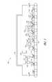
- the automatic solar cell stringer 100can include an enclosure 130 for housing the different equipment required for electrically connecting a plurality of solar cells, a conveyor 132 for loading 131 , processing and unloading 133 a plurality of solar cells, a solder paste applicator 134 having dispenser tubes 136 used to dispense a solder paste 116 on a first and second solar cell 102 , 104 , a vision inspection system 138 for inspecting the solder paste 116 integrity, a robotic arm 140 used to position an interconnect 120 on the solder pads of a third and fourth solar cells 105 , 106 , and a set of hold down pins 150 for pinning down an interconnect 120 to the solder pads of fifth and sixth solar cells 107 , 108 , where the hold down pins 150 also include a soldering mechanism 152 to heat the solder paste 116 into a liquid state 117
- the solder paste 117is allowed to cool down and form a solder joint 118 .
- a plurality of electrically connected solar cells 110are formed.
- the plurality of solar cells 110can be unloaded 133 from the enclosure 130 by the conveyor 132 .
- FIGS. 2-5illustrate operations in the standard process for electrically connecting a plurality of solar cells.
- the operationincludes positioning a first solar cell 102 adjacent to a second solar cell 104 , each solar cell having a plurality of positive solder pads 112 and negative solder pads 114 , where each of the solder pads 112 , 114 are adapted to receive a solder paste 116 .
- the plurality solar cells 103can be aligned using a camera and alignment chuck prior to the application of solder paste 116 .
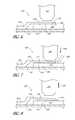
- the operationcan also include placing an interconnect 120 in alignment with the solder pads 112 , 114 of first and second solar cells 102 , 104 .
- the interconnect 120has a main body 122 and tabs 124 positioned over the solder pads 112 , 114 as shown in FIG. 3 .
- the operationcan also include positioning a set of hold down pins 150 above the tabs 124 in preparation for applying a contact force on the tabs 124 as shown in FIGS. 4 and 5 , where FIG. 5 depicts a schematic perspective view of FIG. 4 .
- FIGS. 6-8illustrate cross-sectional representations of an interconnect tab in continuation of the standard process for electrically connecting the plurality of solar cells. For clarity, only a single interconnect tab 120 , second solar cell 104 , hold down pin 150 and work surface 142 are shown, where the operations discussed below are applicable to all similar structures mentioned above.
- the operationcan further include aligning a hold down pin 150 over an interconnect tab 124 , where the tab 124 has a lower surface 129 positioned over a solder pad upper surface 119 of the second solar cell 104 .
- the solder paste 116can be disposed between the tab lower surface 129 and solder pad upper surface 119 , where a working distance 190 separates the lower surface 129 from the upper surface 119 .
- the operationcan also include lowering the hold down pin in a downward direction 154 , pinning the tab lower surface 129 onto the solder pad upper surface 119 .
- the hold down pin 150can be used to conduct heat 156 onto the solder paste 116 thereby heating the solder paste 116 to a liquid state 117 . While the solder paste is in a liquid state 117 , the contact force from the hold down pin 150 can further pin the interconnect tab lower surface 129 to the solder pad upper surface 119 , where the tab 124 downwardly bends in a wedge contacting the solar cell 104 as seen in FIG. 7 .
- the operationalso includes allowing the solder paste 117 to cool, forming a solder joint 118 .
- forming the solder paste in a liquid state 117is performed using standard soldering processes.
- the contact force from the hold down pin 150 on the interconnect tab 124is released by raising the hold down pin 150 in an upward direction 155 as shown in FIG. 8 .
- FIG. 9illustrates a plurality of electrically connected solar cells subsequent to performing the standard processes described in FIGS. 2-8 .
- the plurality of electrically connected solar cells 110includes a first and second solar cell 102 , 104 , an interconnect 120 having a main body 122 and tabs 124 electrically connecting both solar cells 102 , 104 through solder joints 118 .
- solder jointsThe standard method of electrically connecting solar cells discussed above forms thin solder joints, and can result in a wedge-shaped solder joint.
- the solder paste in a liquid state 117can flow unevenly between the lower surface 129 of the tab 124 and the upper surface 119 of the solder pad 114 such that the solder joint 118 formed can be a thin solder joint.
- a thin solder jointcan be weak against mechanical strains, can have a short thermal fatigue life and thus be more frequently prone to failure as compared to uniformly formed solder joints. Because solder paste has a relatively low viscosity when molten it normally is not used alone as a structural joint.
- the contact force from the hold down pin 150is too low, spaces or bubbles in the solder paste 116 , 117 may eventually form micro-voids within the solder joint 118 .
- Micro-voidscan increase the resistance of a solder joint, decreasing the overall current collected from a solar cell.
- a contact force that is too highcould increase the contact pressure on the solder pads 112 , 114 resulting in cracking of the solder pads and damage the solar cell.
- Alternative techniquesinclude manual alignment between the hold down pin 150 , interconnect tab 120 and solder pad 112 , 114 . For narrower or smaller tabs however, the operator may no longer be able to accurately and repeatedly position the hold down pin to the required tolerance, requiring advanced alignment tools which are more costly.
- FIGS. 10-12illustrate a method of electrically connecting a plurality of solar cells.
- the methodcan include positioning a first solar cell 202 adjacent to a second solar cell 204 , each solar cell having a plurality of solder pads 212 , 214 and positioning the solder pads 212 of the first solar cell 202 proximate and perpendicular to the solder pads 214 of the second solar cell 204 .
- the alignment of the first and second solar cells 202 , 204is similar to that of the alignment of the first and second solar cells 102 , 104 in the standard operation of FIG. 2 .
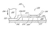
- the methodcan also include aligning a first interconnect 220 to the first and second solar cells 202 , 204 where the first interconnect 220 has a main body 222 and tabs 224 extending therefrom, and where each of the tabs has a downward depression 226 , such that the tabs 224 are positioned above the positive and negative solder pads 212 , 214 of both the first and second solar cells 202 , 204 as seen in FIG. 10 .
- the methodcan also include positioning a set of hold down pins 250 above the tabs 224 in preparation to applying a contact force on the interconnect main body 222 as shown in FIGS. 11 and 12 , where FIG. 12 depicts a schematic perspective view of FIG. 11 .
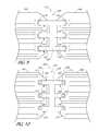
- FIGS. 13-16there are shown cross-sectional representations of an interconnect tab in continuation of the method for electrically connecting the plurality of solar cells of FIGS. 10-12 . Similar to above, only a single interconnect tab 220 , second solar cell 204 , hold down pin 250 and work surface 242 are shown, where the operations discussed below are applicable to all similar structures mentioned above.
- the methodcan further include aligning a hold down pin 250 over the interconnect main body 222 , where a an interconnect tab lower surface 229 is positioned parallel to the solder pad upper surface 219 of the solar cell 204 as shown in FIG. 13 .
- the interconnect tabcan be slightly angled such as in FIG. 14 , where the interconnect tab is a cantilevered tab 225 extending downwardly from the main body of the first interconnect 220 .
- a first working distance 280 , 282can separate the main body 222 from the work surface 242 and a second working distance 290 , 292 can separate the tabs 224 , 225 from the solder pad upper surface 219 .
- the methodcan also include pinning the first interconnect 220 against a work surface 242 by lowering the hold down pin 250 in a downward direction 254 , pressing the hold down pin 250 against the main body 222 such that the tab lower surface 229 is maintained substantially parallel to the solder pad upper surface 219 , and such that the depression 226 substantially flatly contacts the solder pad upper surface 219 as shown in FIG. 15 .
- the methodcan also includes using the hold down pin 250 to conduct heat 256 to form the solder paste 216 into a liquid state 217 .
- the solder paste in a liquid state 217can be formed using any standard soldering processes such as hot soldering or induction soldering. While the solder paste is in a liquid state 217 the tab 224 , 225 can be at a third working distance 294 , where the contact force from the hold down pin 250 can further allow the interconnect tab 224 , 225 to move downwardly toward the solar cell 204 .
- this thickened area of the solder paste 217can be largely, substantially, or continuously in contact with the periphery of the much thinner portion of the solder paste 217 disposed directly between the lower surface 229 and the upper surface 219 of the solar cell 204 .
- the resulting thickened solderafter cooling, can provide a source of material to flow into slip planes caused during fatigue-generated deformations, thereby inhibiting crack growth of the thin portion of the cooled solder layer that is directly between the lower surface 229 and the upper surface 219 of the solar cell 204 .
- the thickened area of solder paste 217can be roughly donut-shaped or toroidal.
- the liquid solder paste 217can flow around the contours associated with such shapes so as to also produce a largely, substantially, or continuously thickened area of solder paste 217 around the corresponding shape of the lower surface 229 .
- the methodcan also include allowing the solder paste 217 to cool down, forming a solder joint 218 similar to the above.
- the methodcan include releasing the contact force between hold down pin 250 and the interconnect main body 222 by raising the hold down pin 250 in an upward direction 255 , where the tab 224 , 225 is a fourth working distance 296 away from the solder pad upper surface 219 as shown in FIG. 16 .
- the interconnect tab 225 of FIG. 14provides a controlled spring force during the process when the main body 222 of the interconnect 220 is pressed against the work surface 242 by the hold down pin 250 minimizing the third working distance.
- the cantilever tab 225provides a finer hold down force as compared to the contact force from the hold down pin 150 of the standard method mentioned above, preventing cracking of the solder pad and damage to the solar cell 204 .
- reducing the size of the cantilever tab 225can provide flexibility against contact stress on the solder pad upper surface 219 also preventing solar cell cracking.
- pinning the hold down pin 250 against the main body 222 of the interconnect 220allows for a contact force in the range of 0-1.0 Newtons between the tab lower surface 229 and the solder pad upper surface 219 .
- the depth of the downward depression 226defines the solder meniscus, where the downward depression 226 controls the solder flux spread.
- FIG. 17illustrates a schematic perspective view of a plurality of electrically connected solar cells subsequent to performing the method of FIGS. 10-16 .
- the plurality of electrically connected solar cells 210includes a first and second solar cell 202 , 204 , an interconnect 220 having a main body 222 and tabs 224 electrically connecting both solar cells 202 , 204 through solder joints 218 .
- electrically connecting a plurality of solar cells 210includes electrically connecting a plurality of solar cells 210 selected from the group containing back-contact solar cells, front-contact solar cells, monocrystalline silicon solar cells, polycrystalline silicon solar cells, amorphous silicon solar cells, thin film silicon solar cells, copper indium gallium selenide (CIGS) solar cells, and cadmium telluride solar cells.
- a plurality of solar cells 210selected from the group containing back-contact solar cells, front-contact solar cells, monocrystalline silicon solar cells, polycrystalline silicon solar cells, amorphous silicon solar cells, thin film silicon solar cells, copper indium gallium selenide (CIGS) solar cells, and cadmium telluride solar cells.
- Some embodiments of these methodscan include positioning a first solar cell 302 adjacent to a second solar cell 304 , each solar cell having a plurality of positive and negative solder pads 312 , 214 .
- the methodcan also include positioning the solder pads 312 of the first solar cell 302 proximate and parallel to the solder pads 314 of the second solar cell 304 .
- the plurality solar cells 303can be aligned using a camera and alignment chuck prior to application of solder paste 316 .
- FIGS. 22-25illustrate cross-sectional representations of an interconnect tab in continuation to the method of electrically connecting solar cells of FIGS. 18-21 . Similar to above, only a single interconnect tab 320 , second solar cell 304 , hold down pin 350 and work surface 342 are shown, where the operations discussed below are applicable to all similar structures mentioned above.
- the methodcan further include aligning a hold down pin 350 over the interconnect main body 322 , where an interconnect tab lower surface 329 is positioned parallel to a solder pad upper surface 319 as shown in FIG. 22 .
- the interconnect tabcan be slightly angled such as in FIG. 23 , where the interconnect tab is a cantilevered tab 325 extending downwardly from the main body of the first interconnect 320 .
- a first working distance 380 , 382can separate the main body 322 from the work surface 342 and a second working distance 390 , 392 can separate the tabs 324 , 325 from the solder pad upper surface 319 .
- the methodcan also include pinning the first interconnect 320 against a work surface 342 by lowering the hold down pin 350 in a downward direction 354 , pressing the hold down pin 350 against the main body 322 such that the tab lower surface 329 is maintained substantially parallel to the solder pad upper surface 319 , and such that the depression 326 substantially flatly contacts the solder pad upper surface 219 as shown in FIG. 24 .
- the methodcan also include using the hold down pin 350 to conduct heat 356 to melt a pre-formed solder paste 316 into a liquid state 317 .
- the methodcan also include releasing the contact force between hold down pin 350 and the interconnect main body 322 by raising the hold down pin 350 in an upward direction 355 , where the tab 324 , 325 is a fourth working distance 396 away from the solder pad upper surface 319 as shown in FIG. 25 .
- the interconnect tab 325 of FIG. 23provides a controlled spring force during the process when the main body 322 of the interconnect 320 is pressed against the work surface 342 by the hold down pin 250 minimizing for the third working distance 394 similar to above.
- the cantilever tab 325provides a finer hold down force as compared to the contact force from the hold down pin 150 of the standard method mentioned above, preventing cracking of the solder pad and damage to the solar cell 304 .
- reducing the size of the cantilever tab 325can provide flexibility against contact stress on the solder pad upper surface 319 also preventing solar cell cracking.
- pinning the hold down pin 350 against the main body 322 of the interconnect 320allows for a contact force in the range of 0-1.0 Newtons between the tab lower surface 329 and the solder pad upper surface 319 .
- the depth of the downward depression 326defines the solder meniscus, where the downward depression 326 controls the solder flux spread.
- FIG. 26illustrates a schematic perspective view of a plurality of electrically connected solar cells subsequent to performing the method of FIGS. 18-25 .
- the plurality of electrically connected solar cells 310can include a first and second solar cell 302 , 304 , an interconnect 320 having a main body 322 and tabs 324 electrically connecting both solar cells 302 , 304 through solder joints 318 .
- the interconnect 120can include a main body 122 and a plurality of tabs 124 .
- the width 260 of the tabs 224can be in the range of 2-10 millimeters and the length 262 of the tab can be in the range of 2-10 millimeters. In other embodiments, the distance between tabs 263 can be in the range of 5-50 millimeters.
- FIG. 30shows the interconnect 220 with a tab 224 in accordance with the embodiment of FIG. 13
- FIG. 31shows the interconnect 220 with a tab 225 in accordance with the embodiment of FIG. 14
- the interconnectcan have a thickness 268 in the range of 50-150 microns and the interconnect tab can have a thickness 264 in the range of 50-150 microns.
- the width 267 of the depressioncan be in the range of 2-10 millimeters.
- the depressioncan have an upper cavity thickness 265 in the range of 10-50 microns and a lower thickness 266 in the range of 10-50 microns.
- FIG. 32illustrates an embodiment of the interconnect from FIGS. 29-31 .
- the interconnect 270can have a main body 272 , tabs 274 , downward depressions 276 and relief features 278 .
- the interconnect 270can be an interconnect used in electrically connecting solar cells manufactured by SunPower Corporation ⁇ .
- the interconnect 270can be used in electrically connecting plurality of solar cells selected from the group containing a back-contact solar cells, front-contact solar cells, monocrystalline silicon solar cells, polycrystalline silicon solar cells, amorphous silicon solar cells, thin film silicon solar cells, copper indium gallium selenide (CIGS) solar cells, and cadmium telluride solar cells.
- CIGScopper indium gallium selenide
- the interconnect 320can have a length 361 in the range of 50-200 millimeters and a width 369 in the range of 8-20 millimeters.
- the interconnect 320can be made of a metal selected from the group containing copper, silver, gold and aluminum.
- the interconnectcan have a thin coating of nickel or tin.
- the interconnect 320includes a main body 322 and a plurality of tabs 324 extending from the main body 322 , and where each of the tabs 324 have a downward depression 326 .
- the width 360 of the tabs 324can be in the range of 2-10 millimeters and the length 362 of the tab can be in the range of 2-10 millimeters. In other embodiments, the distance between tabs 363 can be in the range of 5-50 millimeters.
- FIG. 30shows the interconnect 320 with a tab 324 in accordance with the embodiment of FIG. 22 and FIG. 23 shows the interconnect 320 with a tab 325 in accordance with the embodiment of FIG. 14 .
- the interconnect 320can have a thickness 368 in the range of 50-150 microns and the interconnect 320 tab 324 can have a thickness 364 in the range of 50-150 microns.
- the width 367 of the depression 326can be in the range of 2-10 millimeters.
- the depression 326can have an upper cavity thickness 365 in the range of 10-50 microns and a lower thickness 366 in the range of 10-50 microns.
- FIG. 36illustrates an embodiment of the interconnect from FIGS. 33-35 .
- the interconnect 370can have a main body 372 , tabs 374 , 379 , extruding features 375 , downward depressions 376 , relief features 377 and alignment features 378 .
- the interconnect 370can be an interconnect used in electrically connecting solar cells manufactured by SunPower Corporation ⁇ .
- the interconnect 370can be used in electrically connecting plurality of solar cells selected from the group containing a back-contact solar cells, front-contact solar cells, monocrystalline silicon solar cells, polycrystalline silicon solar cells, amorphous silicon solar cells, thin film silicon solar cells, copper indium gallium selenide (CIGS) solar cells, and cadmium telluride solar cells.
- a back-contact solar cellsfront-contact solar cells
- monocrystalline silicon solar cellspolycrystalline silicon solar cells
- amorphous silicon solar cellsthin film silicon solar cells
- copper indium gallium selenide (CIGS) solar cellscopper indium gallium selenide (CIGS) solar cells
- CGScopper indium gallium selenide
- FIG. 37illustrates a schematic perspective view in accordance with an embodiment of the inventions discussed above.
- the downward depression 226 , 326can be a circular depression 400 , oblong depression 402 , triangular depression 404 , square depression 406 , polygon depression 408 , rectangular depression 410 , and rounded-edge rectangular depression 412 .
- the tabs 224 , 324may have instead an extrusion 414 on the lower surface of the tabs 224 , 324 as also seen below in 434 of FIG. 38 .
- the downward depression 226 , 326can be a partially hollowed depression 420 , regularly hollowed depression 422 , dimple depression 424 , concave depression 426 , square or rectangular depression 428 , partially hollowed rounded-edge rectangular depression 430 , and rounded-edge rectangular depression 432 .
- the tabs 224 , 324may have instead an extrusion 434 on the lower surface of the tabs 224 , 324 .
- FIG. 39illustrates a flow chart of an embodiment of a method for electrically connecting a plurality of solar cells.
- the first operation 500can include providing first and second solar cell 202 , 204 .
- the second operation 502can include positioning the first solar cell 202 adjacent to the second solar cell 204 , each solar cell having a plurality of solder pads 212 , 214 .
- the third operation 504can include aligning a first interconnect 220 to the first and second solar cells 202 , 204 , where the first interconnect 220 has a main body 222 and tabs 224 extending therefrom, and where each of the tabs 224 has a downward depression 226 , such that lower surfaces 229 of the tabs 224 are positioned above the upper surface 219 of the solder pads 212 , 214 of both the first and second solar cells 202 , 204 .
- the last operation 506can include pinning the first interconnect 220 against a work surface 242 by pressing a hold down pin 250 against the main body 222 of the first interconnect 220 such that the lower surfaces 229 of the interconnect tabs 224 are maintained substantially parallel to the upper surfaces 219 of the solder pads 212 , 214 , and such that the depression 226 of each of the tabs 224 substantially flatly contacts one of the solder pads 212 , 214 .
- the last operation 506can include pressing down the main body 222 with sufficient force to cause liquid solder to flow outwardly from the lower surface of the depression 226 toward a periphery of the depression 226 and so as to collect in a second layer of solder around the periphery of the lower surface of the depression 226 .
- the first operation 510can include providing a first and second solar cell 202 , 204 .
- the second operation 512can include positioning the first solar cell 202 adjacent to the second solar cell 204 , each solar cell having a plurality of solder pads 212 , 214 formed in two rows along two opposite edges, and each row of solder pads 212 .
- 214corresponds to and is electrically coupled to the positive or negative electrode of the solar cell 202 , 204 , and where solder pads 212 of a first electrode of the first solar cell 202 are positioned proximate to the solder pads 214 of the opposite electrode of the second solar cell 204 .
- the third operation 514can include aligning a first interconnect 220 to the first and second solar cells 202 , 204 , where the first interconnect 220 has a main body 222 and tabs 224 extending therefrom, and where each of the tabs 224 has a downward depression 226 , such that lower surfaces 219 of the tabs 226 are positioned above the upper surface 319 of the solder pads 212 , 214 of both the first and second solar cells 202 , 204 .
- the fourth operation 516can include pinning the first interconnect 220 against a work surface 242 by pressing a hold down pin 250 against the main body 222 of the first interconnect 220 such that the lower surfaces 229 of the interconnect tabs 224 are maintained substantially parallel to the upper surfaces 219 of the solder pads 212 , 214 , and such that the depression of each of the tabs 224 substantially flatly contacts one of the solder pads 212 , 214 .
- the last operation 518can include forming a solder paste 216 into a liquid state 217 uniformly spread around the depression 226 between the interconnect tabs 224 and solder pads 212 , 214 thereby forming an electrical connection between the first and second solar cells 202 , 204 .
- the last operation 518can include pressing down the main body 222 with sufficient force to cause liquid solder to flow outwardly from the lower surface of the depression 226 toward a periphery of the depression 226 and so as to collect in a second layer of solder around the periphery of the lower surface of the depression 226 .
- FIG. 41illustrates a flow chart of still another embodiment for electrically connecting a plurality of solar cells.
- the first operation 520can include providing a first and second solar cell 202 , 204 .
- the second operation 522can include positioning a first solar cell 202 adjacent to a second solar cell 204 , each solar cell having a plurality of solder pads 212 , 214 , where the solder pads 212 , of the first solar cell 202 are positioned proximate and perpendicular to the solder pads 214 of the second solar cell 204 .
- the third operation 524can include aligning a first interconnect 220 to the first and second solar cells 202 , 204 , where the first interconnect 220 has a main body 222 and cantilevered tabs 225 extending downwardly therefrom, and where each of the tabs 225 has a downward depression 226 with a height in the range of 10-50 microns centrally located near a tab 225 edge, such that lower surfaces 229 of the tabs 225 are positioned above the upper surface 219 of the solder pads 212 , 214 of both the first and second solar cells.
- the fourth operation 526can include pinning the first interconnect 220 against a work surface 242 by pressing down against the main body 222 of the first interconnect 220 such that the lower surfaces 229 of the interconnect tabs 225 maintained substantially parallel to the upper surfaces 219 of the solder pads 212 , 214 , and such that the depression 226 of each of the tabs 225 substantially flatly contacts one of the solder pads 212 , 214 .
- the last operation 528can include forming a solder paste 217 into a liquid state uniformly spread around the depression 226 between the interconnect tabs 225 and solder pads 212 , 214 thereby forming an electrical connection between the first and second solar cells 202 , 204 .
- the cantilevered tabs 225can instead be the interconnect tabs 224 discussed above.
- the last operation 528can include pressing down the main body 222 with sufficient force to cause liquid solder to flow outwardly from the lower surface of the depression 226 toward a periphery of the depression 226 and so as to collect in a second layer of solder around the periphery of the lower surface of the depression 226 .
- the first operation 530can include providing a first and second solar cell 302 , 304 .
- the second operation 532can include positioning a first solar cell 302 adjacent to a second solar cell 304 , each solar cell having a plurality of solder pads 312 , 314 , where the solder pads 312 of the first solar cell 302 are positioned proximate and parallel to the solder pads 314 of the second solar cell 304 .
- the third operation 534can include aligning a first interconnect 320 to the first and second solar cells 302 , 304 , where the first interconnect 320 has a main body 322 and cantilevered tabs 325 extending downward thereform, and where each of the tabs 325 has a downward depression 326 with a height in the range of 10-50 microns centrally located near a tab edge, such that lower surfaces 329 of the tabs 325 are positioned above the upper surface 319 of the solder pads 312 , 314 of both the first and second solar cells 302 , 304 .
- the fourth operation 534can include pinning the first interconnect 320 against a work 342 surface by pressing a hold down pin 350 against the main body 322 of the first interconnect 320 such that the lower surfaces 329 of the interconnect tabs 325 are maintained substantially parallel to the upper surfaces 319 of the solder pads 312 , 314 , and such that the depression 226 of each of the tabs 325 substantially flatly contacts one of the solder pads 312 , 314 .
- the last operation 538can include forming a solder paste into a liquid state 317 uniformly spread around the depression 326 between the interconnect tabs 325 and solder pads 312 , 314 thereby forming an electrical connection between the first and second solar cells 302 , 304 .
- the cantilevered tabs 325can instead be the interconnect tabs 324 discussed above.
- the last operation 538can include pressing down the main body 222 with sufficient force to cause liquid solder to flow outwardly from the lower surface of the depression 226 toward a periphery of the depression 226 and so as to collect in a second layer of solder around the periphery of the lower surface of the depression 226 .
Landscapes
- Engineering & Computer Science (AREA)
- Mechanical Engineering (AREA)
- Computer Hardware Design (AREA)
- Microelectronics & Electronic Packaging (AREA)
- Power Engineering (AREA)
- Manufacturing & Machinery (AREA)
- Photovoltaic Devices (AREA)
Abstract
Description
Claims (19)
Priority Applications (1)
| Application Number | Priority Date | Filing Date | Title |
|---|---|---|---|
| US14/162,619US8991682B2 (en) | 2012-09-28 | 2014-01-23 | Methods and structures for forming and improving solder joint thickness and planarity control features for solar cells |
Applications Claiming Priority (3)
| Application Number | Priority Date | Filing Date | Title |
|---|---|---|---|
| US201261707851P | 2012-09-28 | 2012-09-28 | |
| US13/802,421US8636198B1 (en) | 2012-09-28 | 2013-03-13 | Methods and structures for forming and improving solder joint thickness and planarity control features for solar cells |
| US14/162,619US8991682B2 (en) | 2012-09-28 | 2014-01-23 | Methods and structures for forming and improving solder joint thickness and planarity control features for solar cells |
Related Parent Applications (1)
| Application Number | Title | Priority Date | Filing Date |
|---|---|---|---|
| US13/802,421ContinuationUS8636198B1 (en) | 2012-09-28 | 2013-03-13 | Methods and structures for forming and improving solder joint thickness and planarity control features for solar cells |
Publications (2)
| Publication Number | Publication Date |
|---|---|
| US20140137922A1 US20140137922A1 (en) | 2014-05-22 |
| US8991682B2true US8991682B2 (en) | 2015-03-31 |
Family
ID=49957857
Family Applications (2)
| Application Number | Title | Priority Date | Filing Date |
|---|---|---|---|
| US13/802,421ActiveUS8636198B1 (en) | 2012-09-28 | 2013-03-13 | Methods and structures for forming and improving solder joint thickness and planarity control features for solar cells |
| US14/162,619ActiveUS8991682B2 (en) | 2012-09-28 | 2014-01-23 | Methods and structures for forming and improving solder joint thickness and planarity control features for solar cells |
Family Applications Before (1)
| Application Number | Title | Priority Date | Filing Date |
|---|---|---|---|
| US13/802,421ActiveUS8636198B1 (en) | 2012-09-28 | 2013-03-13 | Methods and structures for forming and improving solder joint thickness and planarity control features for solar cells |
Country Status (9)
| Country | Link |
|---|---|
| US (2) | US8636198B1 (en) |
| JP (1) | JP6345673B2 (en) |
| KR (1) | KR102108913B1 (en) |
| CN (2) | CN104854711B (en) |
| AR (1) | AR092717A1 (en) |
| AU (1) | AU2013323868B2 (en) |
| DE (1) | DE112013004780T5 (en) |
| UY (1) | UY35057A (en) |
| WO (1) | WO2014052244A1 (en) |
Cited By (11)
| Publication number | Priority date | Publication date | Assignee | Title |
|---|---|---|---|---|
| USD822890S1 (en) | 2016-09-07 | 2018-07-10 | Felxtronics Ap, Llc | Lighting apparatus |
| USD832495S1 (en) | 2017-08-18 | 2018-10-30 | Flex Ltd. | Lighting module locking mechanism |
| USD832494S1 (en) | 2017-08-09 | 2018-10-30 | Flex Ltd. | Lighting module heatsink |
| USD833061S1 (en) | 2017-08-09 | 2018-11-06 | Flex Ltd. | Lighting module locking endcap |
| USD846793S1 (en) | 2017-08-09 | 2019-04-23 | Flex Ltd. | Lighting module locking mechanism |
| USD862777S1 (en) | 2017-08-09 | 2019-10-08 | Flex Ltd. | Lighting module wide distribution lens |
| USD862778S1 (en) | 2017-08-22 | 2019-10-08 | Flex Ltd | Lighting module lens |
| USD872319S1 (en) | 2017-08-09 | 2020-01-07 | Flex Ltd. | Lighting module LED light board |
| USD877964S1 (en) | 2017-08-09 | 2020-03-10 | Flex Ltd. | Lighting module |
| USD888323S1 (en) | 2017-09-07 | 2020-06-23 | Flex Ltd | Lighting module wire guard |
| US10775030B2 (en) | 2017-05-05 | 2020-09-15 | Flex Ltd. | Light fixture device including rotatable light modules |
Families Citing this family (20)
| Publication number | Priority date | Publication date | Assignee | Title |
|---|---|---|---|---|
| US8426974B2 (en)* | 2010-09-29 | 2013-04-23 | Sunpower Corporation | Interconnect for an optoelectronic device |
| US8636198B1 (en) | 2012-09-28 | 2014-01-28 | Sunpower Corporation | Methods and structures for forming and improving solder joint thickness and planarity control features for solar cells |
| CN108565254B (en)* | 2013-10-21 | 2021-08-24 | 日本精工株式会社 | semiconductor module |
| US9444004B1 (en)* | 2014-05-02 | 2016-09-13 | Deployable Space Systems, Inc. | System and method for producing modular photovoltaic panel assemblies for space solar arrays |
| DE102015009004A1 (en) | 2015-06-05 | 2016-12-08 | Solaero Technologies Corp. | Automated arrangement and mounting of solar cells on panels for space applications |
| US10276742B2 (en) | 2015-07-09 | 2019-04-30 | Solaero Technologies Corp. | Assembly and mounting of solar cells on space vehicles or satellites |
| US20170040479A1 (en)* | 2015-08-07 | 2017-02-09 | Solaero Technologies Corp. | Reliable interconnection of solar cells |
| JP6399990B2 (en)* | 2015-09-28 | 2018-10-03 | 株式会社豊田自動織機 | Interconnector and solar panel |
| US20170162723A1 (en)* | 2015-12-03 | 2017-06-08 | David Fredric Joel Kavulak | Spot-welded and adhesive-bonded interconnects for solar cells |
| US9899554B2 (en) | 2015-12-14 | 2018-02-20 | Solarcity Corporation | Method of installing a strain relief apparatus to a solar cell |
| JP6509159B2 (en)* | 2016-04-28 | 2019-05-08 | 株式会社豊田自動織機 | Interconnector and solar panel |
| US20170373211A1 (en)* | 2016-06-24 | 2017-12-28 | Merlin Solar Technologies, Inc. | Cell-to-cell interconnect |
| US11575053B2 (en)* | 2017-05-10 | 2023-02-07 | Sharp Kabushiki Kaisha | Photovoltaic device and solar cell module including same |
| KR102521021B1 (en)* | 2018-03-08 | 2023-04-12 | 상라오 징코 솔라 테크놀러지 디벨롭먼트 컴퍼니, 리미티드 | Device and method of coating flux for solar cell panel, and apparatus for attaching interconnector of solar cell panel |
| US11257969B2 (en) | 2018-03-15 | 2022-02-22 | The Boeing Company | Blocking diode board for rollable solar power module |
| CN110767761A (en)* | 2018-07-27 | 2020-02-07 | 上海理想万里晖薄膜设备有限公司 | a photovoltaic module |
| RU2695277C1 (en)* | 2019-02-12 | 2019-07-22 | Общество С Ограниченной Ответственностью "Товарищество Энергетических И Электромобильных Проектов" | Flexible photoelectric module manufacturing method |
| USD993221S1 (en) | 2021-12-24 | 2023-07-25 | Samsung Electronics Co., Ltd. | Remote control |
| US12283640B2 (en) | 2023-04-07 | 2025-04-22 | The Boeing Company | Bypass diode assemblies for a solar cell array |
| CN116944724A (en)* | 2023-08-09 | 2023-10-27 | 晶科能源股份有限公司 | Battery string welding methods and string welding machines |
Citations (138)
| Publication number | Priority date | Publication date | Assignee | Title |
|---|---|---|---|---|
| US3446676A (en) | 1966-09-07 | 1969-05-27 | Webb James E | Solar battery with interconnecting means for plural cells |
| US3574925A (en)* | 1967-12-07 | 1971-04-13 | Licentia Gmbh | Soldering process |
| US4153474A (en) | 1975-12-19 | 1979-05-08 | Erno Raumfahrttechnik Gmbh | Solar energy collector |
| US4301322A (en) | 1980-04-03 | 1981-11-17 | Exxon Research & Engineering Co. | Solar cell with corrugated bus |
| US4323719A (en) | 1979-08-23 | 1982-04-06 | Unisearch Limited | Integrated solar cells and shunting diodes |
| US4373783A (en) | 1980-04-07 | 1983-02-15 | Atlantic Richfield Company | Thermally stabilized heliostat |
| US4456332A (en) | 1980-04-07 | 1984-06-26 | Atlantic Richfield Company | Method of forming structural heliostat |
| US4468849A (en) | 1982-03-08 | 1984-09-04 | Atlantic Richfield Company | Method of making a curved mirror module |
| US4468848A (en) | 1982-03-08 | 1984-09-04 | Atlantic Richfield Company | Method of making combination curved-lightweight mirror module |
| US4481378A (en) | 1982-07-30 | 1984-11-06 | Motorola, Inc. | Protected photovoltaic module |
| US4502200A (en) | 1982-03-08 | 1985-03-05 | Atlantic Richfield Company | Method of preparing lightweight mirror module |
| US4640734A (en) | 1984-05-24 | 1987-02-03 | Atlantic Richfield Company | Method and apparatus for assembling large panels |
| US4643544A (en) | 1985-11-21 | 1987-02-17 | Loughran William P | Three view in one mirror |
| US4643543A (en) | 1986-01-27 | 1987-02-17 | Atlantic Richfield Company | Mirror optic article |
| US4759803A (en) | 1987-08-07 | 1988-07-26 | Applied Solar Energy Corporation | Monolithic solar cell and bypass diode system |
| US5017243A (en)* | 1989-01-06 | 1991-05-21 | Mitsubishi Denki Kabushiki Kaisha | Solar cell and a production method therefor |
| US5180441A (en) | 1991-06-14 | 1993-01-19 | General Dynamics Corporation/Space Systems Division | Solar concentrator array |
| US5248346A (en) | 1989-04-17 | 1993-09-28 | The Boeing Company | Photovoltaic cell and array with inherent bypass diode |
| US5298768A (en) | 1992-02-14 | 1994-03-29 | Sharp Kabushiki Kaisha | Leadless chip-type light emitting element |
| US5334496A (en) | 1992-09-17 | 1994-08-02 | Eastman Kodak Company | Process and apparatus for reproducible production of non-uniform product distributions |
| US5344496A (en) | 1992-11-16 | 1994-09-06 | General Dynamics Corporation, Space Systems Division | Lightweight solar concentrator cell array |
| US5389158A (en) | 1989-04-17 | 1995-02-14 | The Boeing Company | Low bandgap photovoltaic cell with inherent bypass diode |
| US5409549A (en) | 1992-09-03 | 1995-04-25 | Canon Kabushiki Kaisha | Solar cell module panel |
| US5441577A (en)* | 1991-03-07 | 1995-08-15 | Mitsubishi Denki Kabushiki Kaisha | Thin film solar cell and production method therefor |
| US5498297A (en) | 1994-09-15 | 1996-03-12 | Entech, Inc. | Photovoltaic receiver |
| US5580395A (en) | 1994-07-19 | 1996-12-03 | Sharp Kabushiki Kaisha | Solar cell with integrated bypass function |
| US5616185A (en) | 1995-10-10 | 1997-04-01 | Hughes Aircraft Company | Solar cell with integrated bypass diode and method |
| US5660644A (en) | 1995-06-19 | 1997-08-26 | Rockwell International Corporation | Photovoltaic concentrator system |
| US5697192A (en) | 1993-05-18 | 1997-12-16 | Canon Kabushiki Kaisha | Solar cell module and installation method thereof |
| US5865905A (en) | 1996-09-30 | 1999-02-02 | Boeing North American, Inc. | Rolled film solar concentrator |
| US5899199A (en) | 1995-03-28 | 1999-05-04 | Mills; David | Solar energy collector system |
| WO1999057493A1 (en) | 1998-04-30 | 1999-11-11 | Zentrum für Sonnenenergie- und Wasserstoff-Forschung Baden-Württemberg | Thermohydraulic sun-tracking device |
| US5990415A (en) | 1994-12-08 | 1999-11-23 | Pacific Solar Pty Ltd | Multilayer solar cells with bypass diode protection |
| US6034322A (en) | 1999-07-01 | 2000-03-07 | Space Systems/Loral, Inc. | Solar cell assembly |
| US6131565A (en) | 1996-12-20 | 2000-10-17 | Stanwell Corporation Limited | Solar energy collector system |
| US6198171B1 (en) | 1999-12-30 | 2001-03-06 | Siliconware Precision Industries Co., Ltd. | Thermally enhanced quad flat non-lead package of semiconductor |
| JP2001298134A (en) | 2000-04-14 | 2001-10-26 | Mitsubishi Electric Corp | Bypass diode and solar cell module including this bypass diode |
| US6323478B1 (en) | 1997-10-30 | 2001-11-27 | Canon Kabushiki Kaisha | Photovoltaic power generation roof and installation method thereof |
| DE10041271A1 (en) | 2000-08-23 | 2002-03-07 | Thyssen Bausysteme Gmbh | Roofing or wall cladding made of self-supporting sheet metal panels with photovoltaic solar modules attached on the outside and a system on the underside for regulated heat removal and / or supply |
| US6359209B1 (en) | 2000-02-23 | 2002-03-19 | Hughes Electronics Corporation | Solar panel and solar cell having in-plane solar cell interconnect with integrated diode tab |
| US20020059952A1 (en) | 2000-11-21 | 2002-05-23 | Keiji Shimada | Solar battery module, replacement solar cell, and method of replacing solar cell |
| US6402881B1 (en) | 1994-05-09 | 2002-06-11 | The Regents Of The University Of California | Process for electrically interconnecting electrodes |
| US6442937B1 (en) | 2001-08-21 | 2002-09-03 | The Boeing Company | Solar receiver adaptive tracking control |
| US6531328B1 (en) | 2001-10-11 | 2003-03-11 | Solidlite Corporation | Packaging of light-emitting diode |
| US6553729B1 (en) | 2000-06-09 | 2003-04-29 | United Solar Systems Corporation | Self-adhesive photovoltaic module |
| US6607942B1 (en) | 2001-07-26 | 2003-08-19 | Taiwan Semiconductor Manufacturing Company | Method of fabricating as grooved heat spreader for stress reduction in an IC package |
| US6635507B1 (en) | 1999-07-14 | 2003-10-21 | Hughes Electronics Corporation | Monolithic bypass-diode and solar-cell string assembly |
| GB2340993B (en) | 1998-08-19 | 2003-10-29 | British Steel Plc | Integrated photovoltaic composite panel |
| US20040074490A1 (en) | 2001-03-07 | 2004-04-22 | David Mills | Solar energy reflector array |
| DE202004005198U1 (en) | 2004-04-01 | 2004-07-01 | Strebe, Jürgen | Photovoltaic power solar module producing direct current electricity, is mounted directly onto support frame made of metal |
| JP2004253475A (en)* | 2003-02-18 | 2004-09-09 | Sharp Corp | Solar cell module, method of manufacturing solar cell module, and heat source used in the method |
| US20050035444A1 (en) | 2003-08-11 | 2005-02-17 | Siliconware Precision Industries | Multi-chip package device with heat sink and fabrication method thereof |
| US20050268959A1 (en) | 2004-06-04 | 2005-12-08 | Sunpower Corporation | Interconnection of solar cells in a solar cell module |
| JP2006019532A (en) | 2004-07-02 | 2006-01-19 | Sansha Electric Mfg Co Ltd | Solar cell connector |
| US20060054210A1 (en) | 2003-12-15 | 2006-03-16 | Bernard Proisy | Photovoltaic module with an electronic device in the laminated stack |
| US20060060867A1 (en) | 2004-09-09 | 2006-03-23 | Toyoda Gosei Co., Ltd. | Light emitting device |
| US20060097385A1 (en) | 2004-10-25 | 2006-05-11 | Negley Gerald H | Solid metal block semiconductor light emitting device mounting substrates and packages including cavities and heat sinks, and methods of packaging same |
| US20060124953A1 (en) | 2004-12-14 | 2006-06-15 | Negley Gerald H | Semiconductor light emitting device mounting substrates and packages including cavities and cover plates, and methods of packaging same |
| US20060170094A1 (en) | 2005-02-02 | 2006-08-03 | Intel Corporation | Semiconductor package integral heat spreader |
| US7183587B2 (en) | 2003-09-09 | 2007-02-27 | Cree, Inc. | Solid metal block mounting substrates for semiconductor light emitting devices |
| US20070074755A1 (en) | 2005-10-03 | 2007-04-05 | Nanosolar, Inc. | Photovoltaic module with rigidizing backplane |
| US20070151598A1 (en) | 2005-12-21 | 2007-07-05 | Denis De Ceuster | Back side contact solar cell structures and fabrication processes |
| JP2007184542A (en) | 2005-12-09 | 2007-07-19 | Matsushita Electric Ind Co Ltd | LIGHT EMITTING MODULE, ITS MANUFACTURING METHOD, AND BACKLIGHT DEVICE USING THE SAME |
| JP2007194521A (en) | 2006-01-23 | 2007-08-02 | Matsushita Electric Ind Co Ltd | Light emitting module and manufacturing method thereof |
| JP2007214247A (en) | 2006-02-08 | 2007-08-23 | Matsushita Electric Ind Co Ltd | Light emitting module and manufacturing method thereof |
| WO2007096158A1 (en) | 2006-02-23 | 2007-08-30 | Zsw | Solar module system of the parabolic concentrator type |
| US20070257274A1 (en) | 2002-04-10 | 2007-11-08 | Heatron, Inc. | Lighting Device And Method |
| US7304326B2 (en) | 2004-02-06 | 2007-12-04 | Toyoda Gosei Co., Ltd. | Light emitting device and sealing material |
| US20070283996A1 (en)* | 2006-06-13 | 2007-12-13 | Miasole | Photovoltaic module with insulating interconnect carrier |
| US20080011348A1 (en) | 2004-11-25 | 2008-01-17 | Masahiro Aoyama | Solar Cell Module Connector |
| US20080035198A1 (en) | 2004-10-14 | 2008-02-14 | Institut Fur Solarenergieforschung Gmbh | Method for the Contact Separation of Electrically-Conducting Layers on the Back Contacts of Solar Cells and Corresponding Solar Cells |
| WO2008022409A1 (en) | 2006-08-25 | 2008-02-28 | Solar Heat And Power Pty Limited | Energy collector system having east-west extending linear reflectors |
| US20080053523A1 (en)* | 2006-08-30 | 2008-03-06 | Brown Acie | Solar cell interconnect |
| US20080083450A1 (en) | 2006-10-04 | 2008-04-10 | United Technologies Corporation | Thermal management of concentrator photovoltaic cells |
| US20080121266A1 (en)* | 2006-11-29 | 2008-05-29 | Sanyo Electric. Co., Ltd. | Solar cell module |
| US20080230117A1 (en) | 2007-03-20 | 2008-09-25 | Nisshinbo Industries, Inc. | Photovoltaic cell holder for holding a photovoltaic cell and interconnectors |
| JP2008235549A (en) | 2007-03-20 | 2008-10-02 | Sharp Corp | Solar cell device and manufacturing method thereof |
| US20080289680A1 (en) | 2007-05-21 | 2008-11-27 | Macfarlane Alexander T | Photovoltaic module with improved heat transfer and recovery potential |
| WO2008153922A1 (en) | 2007-06-06 | 2008-12-18 | Ausra, Inc. | Integrated solar energy receiver-storage unit |
| US7468485B1 (en) | 2005-08-11 | 2008-12-23 | Sunpower Corporation | Back side contact solar cell with doped polysilicon regions |
| US20090001140A1 (en) | 2006-01-06 | 2009-01-01 | Nisshinbo Industries, Inc. | Method for Soldering Interconnector to Photovoltaic Cell |
| US20090025782A1 (en)* | 2005-06-01 | 2009-01-29 | Shin-Etsu Handotai Co., Ltd. | Solar cell and method for manufacturing the same |
| US20090032093A1 (en) | 2007-07-30 | 2009-02-05 | Lu Fang | Solar Cell Receiver Having An Insulated Bypass Diode |
| US20090032087A1 (en) | 2007-02-06 | 2009-02-05 | Kalejs Juris P | Manufacturing processes for light concentrating solar module |
| KR20090014153A (en) | 2006-05-31 | 2009-02-06 | 덴끼 가가꾸 고교 가부시키가이샤 | LED light source unit |
| WO2009023063A2 (en) | 2007-06-13 | 2009-02-19 | Ausra, Inc. | Solar energy receiver having optically inclined aperture |
| US20090056699A1 (en) | 2007-08-27 | 2009-03-05 | Mills David R | Linear fresnel solar arrays and receievers therefor |
| US20090056785A1 (en) | 2007-09-05 | 2009-03-05 | Skyline Solar, Inc. | Dual trough concentrating solar photovoltaic module |
| US20090056784A1 (en)* | 2005-12-30 | 2009-03-05 | Hubert Reinisch | Solar cell connecting apparatus, strip retaining apparatus and transport apparatus for a solar cell connecting apparatus |
| US20090065043A1 (en)* | 2006-02-22 | 2009-03-12 | Jean-Christophe Hadorn | Method of coupling photovoltaic cells and film for implementing it |
| US20090139557A1 (en) | 2007-11-30 | 2009-06-04 | Douglas Rose | Busbar connection configuration to accommodate for cell misalignment |
| US20090159116A1 (en) | 2005-10-14 | 2009-06-25 | Yoshinobu Umetani | Interconnector, solar cell string using the interconnector and method of manufacturing thereof, and a solar cell module using the solar cell string |
| US7554031B2 (en) | 2005-03-03 | 2009-06-30 | Sunpower Corporation | Preventing harmful polarization of solar cells |
| US20090215304A1 (en) | 2008-02-22 | 2009-08-27 | Thomas Faust | Low profile shunting pv interconnect for solar roofing |
| WO2009110757A2 (en) | 2008-03-06 | 2009-09-11 | Seo Dae-Ho | Photovoltaic assembly |
| US20090266579A1 (en) | 2008-04-04 | 2009-10-29 | Rec Solar As | Interconnector |
| US20090272419A1 (en) | 2006-12-26 | 2009-11-05 | Kyocera Corporation | Solar Cell Module |
| US20090277491A1 (en)* | 2005-10-14 | 2009-11-12 | Sharp Kabushiki Kaisha | Solar Cell, Interconnector-Equipped Solar Cell, Solar Cell String And Solar Cell Module |
| US7714341B2 (en) | 2006-07-07 | 2010-05-11 | Lg Innotek Co., Ltd. | Sub-mount for mounting light emitting device and light emitting device package |
| US20100116323A1 (en)* | 2006-01-27 | 2010-05-13 | Yoshio Katayama | Interconnector, Solar Cell String Using the Interconnector and Method of Manufacturing Thereof, and Solar Cell Module, Using The Solar Cell String |
| US20100139742A1 (en) | 2009-10-12 | 2010-06-10 | Wayman Elizabeth N | Photovoltaic Module Assembly With Integrated Junctions |
| US20100147364A1 (en) | 2008-12-16 | 2010-06-17 | Solopower, Inc. | Thin film photovoltaic module manufacturing methods and structures |
| US20100154788A1 (en) | 2008-12-19 | 2010-06-24 | Skyline Solar, Inc. | Solar receiver |
| US20100163014A1 (en) | 2008-12-29 | 2010-07-01 | Skyline Solar, Inc. | High ground cover ratio solar collection system |
| US20100240153A1 (en)* | 2009-03-23 | 2010-09-23 | Sanyo Electric Co., Ltd. | Manufacture method for photovoltaic module |
| US20100236626A1 (en) | 2009-03-20 | 2010-09-23 | Skyline Solar, Inc. | Reflective surface for solar energy collector |
| US20100263706A1 (en)* | 2007-11-30 | 2010-10-21 | Nobuyuki Isono | Solar cell module and method for manufacturing solar cell module |
| US20100294336A1 (en) | 2009-05-22 | 2010-11-25 | Skyline Solar, Inc. | Center tapped receiver |
| US20100326492A1 (en) | 2009-06-30 | 2010-12-30 | Solarmation, Inc. | Photovoltaic Cell Support Structure Assembly |
| US20110012264A1 (en) | 2009-07-20 | 2011-01-20 | Ryan Linderman | Optoelectronic device with heat spreader unit |
| US20110061724A1 (en) | 2008-03-14 | 2011-03-17 | Kevin Houle | Photovoltaic Cell Module And Method Of Forming Same |
| US20110073165A1 (en)* | 2009-09-28 | 2011-03-31 | Sungeun Lee | Solar cell module and method of manufacturing the same |
| US20110073166A1 (en) | 2009-09-28 | 2011-03-31 | Sungeun Lee | Solar cell module and method of manufacturing the same |
| US20110111534A1 (en) | 2008-04-30 | 2011-05-12 | 3S Swiss Solar Systems Ag | Method for producing a contact for solar cells |
| US20110132457A1 (en) | 2009-12-04 | 2011-06-09 | Skyline Solar, Inc. | Concentrating solar collector with shielding mirrors |
| US7968791B2 (en) | 2009-07-30 | 2011-06-28 | Skyline Solar, Inc. | Solar energy collection system |
| US20110163085A1 (en) | 2008-08-29 | 2011-07-07 | Schmid Technology Systems Gmbh | Method for Soldering Contact Wires to Solar Cells |
| US20110240337A1 (en)* | 2010-04-05 | 2011-10-06 | John Montello | Interconnects for photovoltaic panels |
| US8039777B2 (en) | 2010-07-08 | 2011-10-18 | Skyline Solar, Inc. | Solar collector with reflector having compound curvature |
| US8049150B2 (en) | 2009-01-12 | 2011-11-01 | Skyline Solar, Inc. | Solar collector with end modifications |
| US20110265871A1 (en) | 2010-04-30 | 2011-11-03 | Solar Junction Corporation | Semiconductor solar cell package |
| US20110277814A1 (en)* | 2009-01-29 | 2011-11-17 | Kyocera Corporation | Solar Cell Module and Method of Manufacturing Same |
| US20120034799A1 (en) | 2010-08-03 | 2012-02-09 | Alion, Inc. | Electrical interconnects for photovoltaic modules and methods thereof |
| US8125000B2 (en) | 2008-05-23 | 2012-02-28 | Lg Innotek Co., Ltd. | Light emitting device package having dual recessed substrate |
| US20120074576A1 (en) | 2010-09-29 | 2012-03-29 | Ryan Linderman | Interconnect for an optoelectronic device |
| US20120160294A1 (en)* | 2010-12-23 | 2012-06-28 | Thomas Phu | Method for Connecting Solar Cells |
| US20120285513A1 (en)* | 2009-12-22 | 2012-11-15 | Miasole | Shielding of Interior Diode Assemblies from Compression Forces in Thin-Film Photovoltaic Modules |
| US20130042960A1 (en) | 2010-04-30 | 2013-02-21 | Orthodyne Electronics Corporation | Ultrasonic bonding systems and methods of using the same |
| US20130048047A1 (en) | 2010-09-07 | 2013-02-28 | Sony Chemical & Information Device Corporation | Process for manufacture of solar battery module, solar battery cell connection device, and solar battery module |
| US20130098423A1 (en)* | 2010-07-02 | 2013-04-25 | Mitsubishi Electric Corporation | Solar battery module and manufacturing method thereof |
| US20130112735A1 (en)* | 2010-07-19 | 2013-05-09 | Orthodyne Electronics Corporation | Ultrasonic bonding systems including workholder and ribbon feeding system |
| US20130122632A1 (en)* | 2010-05-31 | 2013-05-16 | Sanyo Electric Co., Ltd. | Method of manufacturing solar cell module |
| US20130206062A1 (en) | 2012-02-10 | 2013-08-15 | Palo Alto Research Center Incoproated | Micro-Extrusion Printhead With Offset Orifices For Generating Gridlines On Non-Square Substrates |
| US20130206204A1 (en)* | 2011-06-28 | 2013-08-15 | Panasonic Corporation | Solar cell module |
| US20130233375A1 (en)* | 2010-12-21 | 2013-09-12 | Mitsubishi Electric Corporation | Solar cell module and manufacturing method thereof |
| US20130255748A1 (en)* | 2011-02-16 | 2013-10-03 | Mitsubishi Electric Corporation | Solar battery cell, solar battery module, and joining method of lead wire of solar battery cell |
| US8636198B1 (en) | 2012-09-28 | 2014-01-28 | Sunpower Corporation | Methods and structures for forming and improving solder joint thickness and planarity control features for solar cells |
| US20140048306A1 (en)* | 2012-08-14 | 2014-02-20 | Au Optronics Corporation | Apparatus for Patterning Ribbon, String Tabbing Method and Solar Cell Module Using the Same |
Family Cites Families (18)
| Publication number | Priority date | Publication date | Assignee | Title |
|---|---|---|---|---|
| US3340096A (en)* | 1962-02-26 | 1967-09-05 | Spectrolab A Division Of Textr | Solar cell array |
| US3459597A (en)* | 1966-02-04 | 1969-08-05 | Trw Inc | Solar cells with flexible overlapping bifurcated connector |
| JPS6063975U (en)* | 1983-10-05 | 1985-05-07 | シャープ株式会社 | Lead plate |
| JP3122536B2 (en)* | 1992-08-03 | 2001-01-09 | シャープ株式会社 | Solar cell module |
| EP0839321B1 (en)* | 1996-05-17 | 2006-01-11 | FormFactor, Inc. | Contact tip structures for microelectronic interconnection elements and methods of making same |
| JP2002094090A (en)* | 2000-09-11 | 2002-03-29 | Honda Motor Co Ltd | Wiring material for solar cell module and connection method thereof |
| EP1359625B1 (en)* | 2000-12-28 | 2010-10-06 | Mitsubishi Denki Kabushiki Kaisha | Solar battery |
| JP4526223B2 (en)* | 2001-06-29 | 2010-08-18 | シャープ株式会社 | Wiring member, solar cell module and manufacturing method thereof |
| JP4509835B2 (en)* | 2004-03-29 | 2010-07-21 | パナソニック株式会社 | Cell, package device, and method for manufacturing package device |
| JP2005347703A (en)* | 2004-06-07 | 2005-12-15 | Npc:Kk | Tab lead fitting equipment for solar battery cell |
| DE102006019638A1 (en)* | 2006-04-25 | 2007-11-08 | Solarwatt Ag | Line connector for solar cells of plate-shaped solar modules, has supply lines arranged in acute-angle manner at band-shaped carrier unit so that center line of supply lines is attached at center line of carrier unit in acute-angle manner |
| US9184327B2 (en)* | 2006-10-03 | 2015-11-10 | Sunpower Corporation | Formed photovoltaic module busbars |
| JP2008147260A (en)* | 2006-12-06 | 2008-06-26 | Sharp Corp | Interconnector, solar cell string, solar cell module, and solar cell module manufacturing method |
| US20100038358A1 (en)* | 2008-03-20 | 2010-02-18 | Dingle Brad M | Inductive soldering device |
| JP2010129675A (en)* | 2008-11-26 | 2010-06-10 | Sharp Corp | Laser joining method, method of manufacturing solar cell, and solar cell manufacturing device |
| US20110146778A1 (en)* | 2009-12-22 | 2011-06-23 | Miasole | Shielding of interior diode assemblies from compression forces in thin-film photovoltaic modules |
| TWI440196B (en)* | 2011-07-12 | 2014-06-01 | Au Optronics Corp | Back electrode solar battery module and electrode welding method thereof |
| TWI435456B (en)* | 2011-08-18 | 2014-04-21 | Au Optronics Corp | Electrode soldering structure, back contact solar module, and method of manufacturing solar module |
- 2013
- 2013-03-13USUS13/802,421patent/US8636198B1/enactiveActive
- 2013-09-23JPJP2015534583Apatent/JP6345673B2/enactiveActive
- 2013-09-23DEDE112013004780.2Tpatent/DE112013004780T5/ennot_activeWithdrawn
- 2013-09-23CNCN201380056336.3Apatent/CN104854711B/enactiveActive
- 2013-09-23CNCN201710339555.2Apatent/CN107393993B/enactiveActive
- 2013-09-23AUAU2013323868Apatent/AU2013323868B2/enactiveActive
- 2013-09-23WOPCT/US2013/061231patent/WO2014052244A1/enactiveApplication Filing
- 2013-09-23KRKR1020157010589Apatent/KR102108913B1/enactiveActive
- 2013-09-27UYUY0001035057Apatent/UY35057A/ennot_activeApplication Discontinuation
- 2013-09-27ARARP130103490Apatent/AR092717A1/enunknown
- 2014
- 2014-01-23USUS14/162,619patent/US8991682B2/enactiveActive
Patent Citations (160)
| Publication number | Priority date | Publication date | Assignee | Title |
|---|---|---|---|---|
| US3446676A (en) | 1966-09-07 | 1969-05-27 | Webb James E | Solar battery with interconnecting means for plural cells |
| US3574925A (en)* | 1967-12-07 | 1971-04-13 | Licentia Gmbh | Soldering process |
| US4153474A (en) | 1975-12-19 | 1979-05-08 | Erno Raumfahrttechnik Gmbh | Solar energy collector |
| US4323719A (en) | 1979-08-23 | 1982-04-06 | Unisearch Limited | Integrated solar cells and shunting diodes |
| US4301322A (en) | 1980-04-03 | 1981-11-17 | Exxon Research & Engineering Co. | Solar cell with corrugated bus |
| US4373783A (en) | 1980-04-07 | 1983-02-15 | Atlantic Richfield Company | Thermally stabilized heliostat |
| US4456332A (en) | 1980-04-07 | 1984-06-26 | Atlantic Richfield Company | Method of forming structural heliostat |
| US4502200A (en) | 1982-03-08 | 1985-03-05 | Atlantic Richfield Company | Method of preparing lightweight mirror module |
| US4468848A (en) | 1982-03-08 | 1984-09-04 | Atlantic Richfield Company | Method of making combination curved-lightweight mirror module |
| US4468849A (en) | 1982-03-08 | 1984-09-04 | Atlantic Richfield Company | Method of making a curved mirror module |
| US4481378A (en) | 1982-07-30 | 1984-11-06 | Motorola, Inc. | Protected photovoltaic module |
| US4640734A (en) | 1984-05-24 | 1987-02-03 | Atlantic Richfield Company | Method and apparatus for assembling large panels |
| US4643544A (en) | 1985-11-21 | 1987-02-17 | Loughran William P | Three view in one mirror |
| US4643543A (en) | 1986-01-27 | 1987-02-17 | Atlantic Richfield Company | Mirror optic article |
| US4759803A (en) | 1987-08-07 | 1988-07-26 | Applied Solar Energy Corporation | Monolithic solar cell and bypass diode system |
| US5017243A (en)* | 1989-01-06 | 1991-05-21 | Mitsubishi Denki Kabushiki Kaisha | Solar cell and a production method therefor |
| US5248346A (en) | 1989-04-17 | 1993-09-28 | The Boeing Company | Photovoltaic cell and array with inherent bypass diode |
| US5389158A (en) | 1989-04-17 | 1995-02-14 | The Boeing Company | Low bandgap photovoltaic cell with inherent bypass diode |
| US5441577A (en)* | 1991-03-07 | 1995-08-15 | Mitsubishi Denki Kabushiki Kaisha | Thin film solar cell and production method therefor |
| US5180441A (en) | 1991-06-14 | 1993-01-19 | General Dynamics Corporation/Space Systems Division | Solar concentrator array |
| US5298768A (en) | 1992-02-14 | 1994-03-29 | Sharp Kabushiki Kaisha | Leadless chip-type light emitting element |
| US5409549A (en) | 1992-09-03 | 1995-04-25 | Canon Kabushiki Kaisha | Solar cell module panel |
| US5334496A (en) | 1992-09-17 | 1994-08-02 | Eastman Kodak Company | Process and apparatus for reproducible production of non-uniform product distributions |
| US5344496A (en) | 1992-11-16 | 1994-09-06 | General Dynamics Corporation, Space Systems Division | Lightweight solar concentrator cell array |
| US5697192A (en) | 1993-05-18 | 1997-12-16 | Canon Kabushiki Kaisha | Solar cell module and installation method thereof |
| US6402881B1 (en) | 1994-05-09 | 2002-06-11 | The Regents Of The University Of California | Process for electrically interconnecting electrodes |
| US5580395A (en) | 1994-07-19 | 1996-12-03 | Sharp Kabushiki Kaisha | Solar cell with integrated bypass function |
| US5498297A (en) | 1994-09-15 | 1996-03-12 | Entech, Inc. | Photovoltaic receiver |
| US5990415A (en) | 1994-12-08 | 1999-11-23 | Pacific Solar Pty Ltd | Multilayer solar cells with bypass diode protection |
| US5899199A (en) | 1995-03-28 | 1999-05-04 | Mills; David | Solar energy collector system |
| US5660644A (en) | 1995-06-19 | 1997-08-26 | Rockwell International Corporation | Photovoltaic concentrator system |
| US5616185A (en) | 1995-10-10 | 1997-04-01 | Hughes Aircraft Company | Solar cell with integrated bypass diode and method |
| US5865905A (en) | 1996-09-30 | 1999-02-02 | Boeing North American, Inc. | Rolled film solar concentrator |
| US6131565A (en) | 1996-12-20 | 2000-10-17 | Stanwell Corporation Limited | Solar energy collector system |
| US6323478B1 (en) | 1997-10-30 | 2001-11-27 | Canon Kabushiki Kaisha | Photovoltaic power generation roof and installation method thereof |
| WO1999057493A1 (en) | 1998-04-30 | 1999-11-11 | Zentrum für Sonnenenergie- und Wasserstoff-Forschung Baden-Württemberg | Thermohydraulic sun-tracking device |
| GB2340993B (en) | 1998-08-19 | 2003-10-29 | British Steel Plc | Integrated photovoltaic composite panel |
| US6034322A (en) | 1999-07-01 | 2000-03-07 | Space Systems/Loral, Inc. | Solar cell assembly |
| US6635507B1 (en) | 1999-07-14 | 2003-10-21 | Hughes Electronics Corporation | Monolithic bypass-diode and solar-cell string assembly |
| US6198171B1 (en) | 1999-12-30 | 2001-03-06 | Siliconware Precision Industries Co., Ltd. | Thermally enhanced quad flat non-lead package of semiconductor |
| US6359209B1 (en) | 2000-02-23 | 2002-03-19 | Hughes Electronics Corporation | Solar panel and solar cell having in-plane solar cell interconnect with integrated diode tab |
| JP2001298134A (en) | 2000-04-14 | 2001-10-26 | Mitsubishi Electric Corp | Bypass diode and solar cell module including this bypass diode |
| US6553729B1 (en) | 2000-06-09 | 2003-04-29 | United Solar Systems Corporation | Self-adhesive photovoltaic module |
| DE10041271A1 (en) | 2000-08-23 | 2002-03-07 | Thyssen Bausysteme Gmbh | Roofing or wall cladding made of self-supporting sheet metal panels with photovoltaic solar modules attached on the outside and a system on the underside for regulated heat removal and / or supply |
| US20020059952A1 (en) | 2000-11-21 | 2002-05-23 | Keiji Shimada | Solar battery module, replacement solar cell, and method of replacing solar cell |
| US20040074490A1 (en) | 2001-03-07 | 2004-04-22 | David Mills | Solar energy reflector array |
| US6607942B1 (en) | 2001-07-26 | 2003-08-19 | Taiwan Semiconductor Manufacturing Company | Method of fabricating as grooved heat spreader for stress reduction in an IC package |
| US6442937B1 (en) | 2001-08-21 | 2002-09-03 | The Boeing Company | Solar receiver adaptive tracking control |
| US6531328B1 (en) | 2001-10-11 | 2003-03-11 | Solidlite Corporation | Packaging of light-emitting diode |
| US20070257274A1 (en) | 2002-04-10 | 2007-11-08 | Heatron, Inc. | Lighting Device And Method |
| JP2004253475A (en)* | 2003-02-18 | 2004-09-09 | Sharp Corp | Solar cell module, method of manufacturing solar cell module, and heat source used in the method |
| US20050035444A1 (en) | 2003-08-11 | 2005-02-17 | Siliconware Precision Industries | Multi-chip package device with heat sink and fabrication method thereof |
| US7183587B2 (en) | 2003-09-09 | 2007-02-27 | Cree, Inc. | Solid metal block mounting substrates for semiconductor light emitting devices |
| US20060054210A1 (en) | 2003-12-15 | 2006-03-16 | Bernard Proisy | Photovoltaic module with an electronic device in the laminated stack |
| US7304326B2 (en) | 2004-02-06 | 2007-12-04 | Toyoda Gosei Co., Ltd. | Light emitting device and sealing material |
| DE202004005198U1 (en) | 2004-04-01 | 2004-07-01 | Strebe, Jürgen | Photovoltaic power solar module producing direct current electricity, is mounted directly onto support frame made of metal |
| US20050268959A1 (en) | 2004-06-04 | 2005-12-08 | Sunpower Corporation | Interconnection of solar cells in a solar cell module |
| JP2006019532A (en) | 2004-07-02 | 2006-01-19 | Sansha Electric Mfg Co Ltd | Solar cell connector |
| US20060060867A1 (en) | 2004-09-09 | 2006-03-23 | Toyoda Gosei Co., Ltd. | Light emitting device |
| US20080035198A1 (en) | 2004-10-14 | 2008-02-14 | Institut Fur Solarenergieforschung Gmbh | Method for the Contact Separation of Electrically-Conducting Layers on the Back Contacts of Solar Cells and Corresponding Solar Cells |
| US20060097385A1 (en) | 2004-10-25 | 2006-05-11 | Negley Gerald H | Solid metal block semiconductor light emitting device mounting substrates and packages including cavities and heat sinks, and methods of packaging same |
| KR20070070183A (en) | 2004-10-25 | 2007-07-03 | 크리 인코포레이티드 | Substrate, package, and method for packaging the solid state metal block semiconductor light emitting device including the cavity and the heat sink |
| US7906793B2 (en) | 2004-10-25 | 2011-03-15 | Cree, Inc. | Solid metal block semiconductor light emitting device mounting substrates |
| US20090134421A1 (en) | 2004-10-25 | 2009-05-28 | Cree, Inc. | Solid metal block semiconductor light emitting device mounting substrates and packages |
| US20080011348A1 (en) | 2004-11-25 | 2008-01-17 | Masahiro Aoyama | Solar Cell Module Connector |
| US20060124953A1 (en) | 2004-12-14 | 2006-06-15 | Negley Gerald H | Semiconductor light emitting device mounting substrates and packages including cavities and cover plates, and methods of packaging same |
| US20060170094A1 (en) | 2005-02-02 | 2006-08-03 | Intel Corporation | Semiconductor package integral heat spreader |
| US7554031B2 (en) | 2005-03-03 | 2009-06-30 | Sunpower Corporation | Preventing harmful polarization of solar cells |
| US20090025782A1 (en)* | 2005-06-01 | 2009-01-29 | Shin-Etsu Handotai Co., Ltd. | Solar cell and method for manufacturing the same |
| US7468485B1 (en) | 2005-08-11 | 2008-12-23 | Sunpower Corporation | Back side contact solar cell with doped polysilicon regions |
| US20070074755A1 (en) | 2005-10-03 | 2007-04-05 | Nanosolar, Inc. | Photovoltaic module with rigidizing backplane |
| US20090159116A1 (en) | 2005-10-14 | 2009-06-25 | Yoshinobu Umetani | Interconnector, solar cell string using the interconnector and method of manufacturing thereof, and a solar cell module using the solar cell string |
| US20090277491A1 (en)* | 2005-10-14 | 2009-11-12 | Sharp Kabushiki Kaisha | Solar Cell, Interconnector-Equipped Solar Cell, Solar Cell String And Solar Cell Module |
| JP2007184542A (en) | 2005-12-09 | 2007-07-19 | Matsushita Electric Ind Co Ltd | LIGHT EMITTING MODULE, ITS MANUFACTURING METHOD, AND BACKLIGHT DEVICE USING THE SAME |
| US20070151598A1 (en) | 2005-12-21 | 2007-07-05 | Denis De Ceuster | Back side contact solar cell structures and fabrication processes |
| US20090056784A1 (en)* | 2005-12-30 | 2009-03-05 | Hubert Reinisch | Solar cell connecting apparatus, strip retaining apparatus and transport apparatus for a solar cell connecting apparatus |
| US20090001140A1 (en) | 2006-01-06 | 2009-01-01 | Nisshinbo Industries, Inc. | Method for Soldering Interconnector to Photovoltaic Cell |
| JP2007194521A (en) | 2006-01-23 | 2007-08-02 | Matsushita Electric Ind Co Ltd | Light emitting module and manufacturing method thereof |
| US20100116323A1 (en)* | 2006-01-27 | 2010-05-13 | Yoshio Katayama | Interconnector, Solar Cell String Using the Interconnector and Method of Manufacturing Thereof, and Solar Cell Module, Using The Solar Cell String |
| JP2007214247A (en) | 2006-02-08 | 2007-08-23 | Matsushita Electric Ind Co Ltd | Light emitting module and manufacturing method thereof |
| US20090065043A1 (en)* | 2006-02-22 | 2009-03-12 | Jean-Christophe Hadorn | Method of coupling photovoltaic cells and film for implementing it |
| US20090095284A1 (en) | 2006-02-23 | 2009-04-16 | Fritz Klotz | Solar Module System With Support Structure |
| WO2007096158A1 (en) | 2006-02-23 | 2007-08-30 | Zsw | Solar module system of the parabolic concentrator type |
| US20100319682A1 (en) | 2006-02-23 | 2010-12-23 | Zentrum Fuer Sonnenenergie-Und Wasserstoff- Forschung Baden-Wuert-Temberg | Solar Module System of the Parabolic Concentrator Type |
| WO2007096157A3 (en) | 2006-02-23 | 2007-12-27 | Zsw | Solar module system with support structure |
| KR20090014153A (en) | 2006-05-31 | 2009-02-06 | 덴끼 가가꾸 고교 가부시키가이샤 | LED light source unit |
| US20070283996A1 (en)* | 2006-06-13 | 2007-12-13 | Miasole | Photovoltaic module with insulating interconnect carrier |
| US7714341B2 (en) | 2006-07-07 | 2010-05-11 | Lg Innotek Co., Ltd. | Sub-mount for mounting light emitting device and light emitting device package |
| WO2008022409A1 (en) | 2006-08-25 | 2008-02-28 | Solar Heat And Power Pty Limited | Energy collector system having east-west extending linear reflectors |
| US20080053523A1 (en)* | 2006-08-30 | 2008-03-06 | Brown Acie | Solar cell interconnect |
| US20080083450A1 (en) | 2006-10-04 | 2008-04-10 | United Technologies Corporation | Thermal management of concentrator photovoltaic cells |
| US20080121266A1 (en)* | 2006-11-29 | 2008-05-29 | Sanyo Electric. Co., Ltd. | Solar cell module |
| US20090272419A1 (en) | 2006-12-26 | 2009-11-05 | Kyocera Corporation | Solar Cell Module |
| US20090032087A1 (en) | 2007-02-06 | 2009-02-05 | Kalejs Juris P | Manufacturing processes for light concentrating solar module |
| JP2008235549A (en) | 2007-03-20 | 2008-10-02 | Sharp Corp | Solar cell device and manufacturing method thereof |
| US20080230117A1 (en) | 2007-03-20 | 2008-09-25 | Nisshinbo Industries, Inc. | Photovoltaic cell holder for holding a photovoltaic cell and interconnectors |
| US20080289680A1 (en) | 2007-05-21 | 2008-11-27 | Macfarlane Alexander T | Photovoltaic module with improved heat transfer and recovery potential |
| WO2008153922A1 (en) | 2007-06-06 | 2008-12-18 | Ausra, Inc. | Integrated solar energy receiver-storage unit |
| WO2009023063A2 (en) | 2007-06-13 | 2009-02-19 | Ausra, Inc. | Solar energy receiver having optically inclined aperture |
| US20090032093A1 (en) | 2007-07-30 | 2009-02-05 | Lu Fang | Solar Cell Receiver Having An Insulated Bypass Diode |
| US20090056699A1 (en) | 2007-08-27 | 2009-03-05 | Mills David R | Linear fresnel solar arrays and receievers therefor |
| WO2009029275A3 (en) | 2007-08-27 | 2009-08-06 | Ausra Inc | Linear fresnel solar arrays and components therefor |
| WO2009029277A3 (en) | 2007-08-27 | 2009-08-13 | Ausra Inc | Linear fresnel solar arrays |
| US7820906B2 (en) | 2007-09-05 | 2010-10-26 | Skyline Solar, Inc. | Photovoltaic receiver |
| US20090056785A1 (en) | 2007-09-05 | 2009-03-05 | Skyline Solar, Inc. | Dual trough concentrating solar photovoltaic module |
| US7709730B2 (en) | 2007-09-05 | 2010-05-04 | Skyline Solar, Inc. | Dual trough concentrating solar photovoltaic module |
| US20110226310A1 (en) | 2007-09-05 | 2011-09-22 | Skyline Solar, Inc. | Solar energy collection system |
| US7932461B2 (en) | 2007-09-05 | 2011-04-26 | Skyline Solar, Inc. | Solar collector framework |
| US20090056786A1 (en) | 2007-09-05 | 2009-03-05 | Skyline Solar, Inc. | Photovoltaic receiver |
| US20090056787A1 (en) | 2007-09-05 | 2009-03-05 | Skyline Solar, Inc. | Concentrating solar collector |
| US7825327B2 (en) | 2007-09-05 | 2010-11-02 | Skyline Solar, Inc. | Concentrating solar collector |
| US20100193014A1 (en) | 2007-09-05 | 2010-08-05 | Skyline Solar, Inc. | Photovoltaic receiver |
| US20100263706A1 (en)* | 2007-11-30 | 2010-10-21 | Nobuyuki Isono | Solar cell module and method for manufacturing solar cell module |
| US20090139557A1 (en) | 2007-11-30 | 2009-06-04 | Douglas Rose | Busbar connection configuration to accommodate for cell misalignment |
| US20090215304A1 (en) | 2008-02-22 | 2009-08-27 | Thomas Faust | Low profile shunting pv interconnect for solar roofing |
| US20110030764A1 (en) | 2008-03-06 | 2011-02-10 | Dae-Ho Seo | Photovoltaic cell assembly |
| WO2009110757A2 (en) | 2008-03-06 | 2009-09-11 | Seo Dae-Ho | Photovoltaic assembly |
| US20110061724A1 (en) | 2008-03-14 | 2011-03-17 | Kevin Houle | Photovoltaic Cell Module And Method Of Forming Same |
| US20090266579A1 (en) | 2008-04-04 | 2009-10-29 | Rec Solar As | Interconnector |
| US20110111534A1 (en) | 2008-04-30 | 2011-05-12 | 3S Swiss Solar Systems Ag | Method for producing a contact for solar cells |
| US8125000B2 (en) | 2008-05-23 | 2012-02-28 | Lg Innotek Co., Ltd. | Light emitting device package having dual recessed substrate |
| US20110163085A1 (en) | 2008-08-29 | 2011-07-07 | Schmid Technology Systems Gmbh | Method for Soldering Contact Wires to Solar Cells |
| US20100147364A1 (en) | 2008-12-16 | 2010-06-17 | Solopower, Inc. | Thin film photovoltaic module manufacturing methods and structures |
| US20100154788A1 (en) | 2008-12-19 | 2010-06-24 | Skyline Solar, Inc. | Solar receiver |
| US20100163014A1 (en) | 2008-12-29 | 2010-07-01 | Skyline Solar, Inc. | High ground cover ratio solar collection system |
| US8049150B2 (en) | 2009-01-12 | 2011-11-01 | Skyline Solar, Inc. | Solar collector with end modifications |
| US20110277814A1 (en)* | 2009-01-29 | 2011-11-17 | Kyocera Corporation | Solar Cell Module and Method of Manufacturing Same |
| US20100236626A1 (en) | 2009-03-20 | 2010-09-23 | Skyline Solar, Inc. | Reflective surface for solar energy collector |
| US7952057B2 (en) | 2009-03-20 | 2011-05-31 | Skyline Solar, Inc. | Reflective surface for solar energy collector |
| US20110186130A1 (en) | 2009-03-20 | 2011-08-04 | Skyline Solar, Inc. | Reflective surface for solar energy collector |
| US20100240153A1 (en)* | 2009-03-23 | 2010-09-23 | Sanyo Electric Co., Ltd. | Manufacture method for photovoltaic module |
| US20100294336A1 (en) | 2009-05-22 | 2010-11-25 | Skyline Solar, Inc. | Center tapped receiver |
| US20100326492A1 (en) | 2009-06-30 | 2010-12-30 | Solarmation, Inc. | Photovoltaic Cell Support Structure Assembly |
| US20110012264A1 (en) | 2009-07-20 | 2011-01-20 | Ryan Linderman | Optoelectronic device with heat spreader unit |
| US20120012156A1 (en) | 2009-07-20 | 2012-01-19 | Ryan Linderman | Optoelectronic device with heat spreader unit |
| US8530990B2 (en) | 2009-07-20 | 2013-09-10 | Sunpower Corporation | Optoelectronic device with heat spreader unit |
| US7968791B2 (en) | 2009-07-30 | 2011-06-28 | Skyline Solar, Inc. | Solar energy collection system |
| US20110073165A1 (en)* | 2009-09-28 | 2011-03-31 | Sungeun Lee | Solar cell module and method of manufacturing the same |
| US20110073166A1 (en) | 2009-09-28 | 2011-03-31 | Sungeun Lee | Solar cell module and method of manufacturing the same |
| US20100139742A1 (en) | 2009-10-12 | 2010-06-10 | Wayman Elizabeth N | Photovoltaic Module Assembly With Integrated Junctions |
| US20110132457A1 (en) | 2009-12-04 | 2011-06-09 | Skyline Solar, Inc. | Concentrating solar collector with shielding mirrors |
| US20120285513A1 (en)* | 2009-12-22 | 2012-11-15 | Miasole | Shielding of Interior Diode Assemblies from Compression Forces in Thin-Film Photovoltaic Modules |
| US20110240337A1 (en)* | 2010-04-05 | 2011-10-06 | John Montello | Interconnects for photovoltaic panels |
| US20110265871A1 (en) | 2010-04-30 | 2011-11-03 | Solar Junction Corporation | Semiconductor solar cell package |
| US20130042960A1 (en) | 2010-04-30 | 2013-02-21 | Orthodyne Electronics Corporation | Ultrasonic bonding systems and methods of using the same |
| US20130122632A1 (en)* | 2010-05-31 | 2013-05-16 | Sanyo Electric Co., Ltd. | Method of manufacturing solar cell module |
| US20130098423A1 (en)* | 2010-07-02 | 2013-04-25 | Mitsubishi Electric Corporation | Solar battery module and manufacturing method thereof |
| US8071930B2 (en) | 2010-07-08 | 2011-12-06 | SkylineSolar, Inc. | Solar collector having a spaced frame support structure with a multiplicity of linear struts |
| US8039777B2 (en) | 2010-07-08 | 2011-10-18 | Skyline Solar, Inc. | Solar collector with reflector having compound curvature |
| US20130112735A1 (en)* | 2010-07-19 | 2013-05-09 | Orthodyne Electronics Corporation | Ultrasonic bonding systems including workholder and ribbon feeding system |
| US20120034799A1 (en) | 2010-08-03 | 2012-02-09 | Alion, Inc. | Electrical interconnects for photovoltaic modules and methods thereof |
| US20130048047A1 (en) | 2010-09-07 | 2013-02-28 | Sony Chemical & Information Device Corporation | Process for manufacture of solar battery module, solar battery cell connection device, and solar battery module |
| US20120074576A1 (en) | 2010-09-29 | 2012-03-29 | Ryan Linderman | Interconnect for an optoelectronic device |
| US20130233375A1 (en)* | 2010-12-21 | 2013-09-12 | Mitsubishi Electric Corporation | Solar cell module and manufacturing method thereof |
| US20120160294A1 (en)* | 2010-12-23 | 2012-06-28 | Thomas Phu | Method for Connecting Solar Cells |
| US20130255748A1 (en)* | 2011-02-16 | 2013-10-03 | Mitsubishi Electric Corporation | Solar battery cell, solar battery module, and joining method of lead wire of solar battery cell |
| US20130206204A1 (en)* | 2011-06-28 | 2013-08-15 | Panasonic Corporation | Solar cell module |
| US20130206062A1 (en) | 2012-02-10 | 2013-08-15 | Palo Alto Research Center Incoproated | Micro-Extrusion Printhead With Offset Orifices For Generating Gridlines On Non-Square Substrates |
| US20140048306A1 (en)* | 2012-08-14 | 2014-02-20 | Au Optronics Corporation | Apparatus for Patterning Ribbon, String Tabbing Method and Solar Cell Module Using the Same |
| US8636198B1 (en) | 2012-09-28 | 2014-01-28 | Sunpower Corporation | Methods and structures for forming and improving solder joint thickness and planarity control features for solar cells |
Non-Patent Citations (11)
| Title |
|---|
| Bardwell, Karen et al., "Minimizing End Shadowing Effects on Parabolic Concentrator Arrays," IEEE, 1980, pp. 765-770. |
| Carroll, Don et al. "Production of the Alpha Solarco Proof-of-Concept Array," IEEE, 1990, pp. 1136-1141. |
| Edenburn, Michael W., et al. "Shading Analysis of a Photovoltaic Cell String Illuminated by a Parabolic Trough Concentrator," IEEE, 1981, pp. 63-68. |
| International Search Report and Written Opinion dated Jan. 25, 2011, International Appl. No. PCT/US2010/040884, 6 pages. |
| International Search Report and Written Opinion dated Jul. 21, 2011, International Appl. No. PCT/US2010/056386 (filed Nov. 11, 2010), 10 pages. |
| International Search Report and Written Opinion issued Jan. 21, 2014, International Appl. No. PCT/US2013/061231, 11 pages. |
| International Search Report and Written Opinion of PCT/US2011/044747, filed Jul. 20, 2011, dated Mar. 6, 2012. |
| Quagan, Robert J., "Laser Diode Heat Spreaders," Ion Beam Milling, Inc., website copyright 2010, http://www.ionbeammilling.com/default.asp, 9 pgs. |
| Shepard, Jr., N. F. et al., "The Integration of Bypass Diodes with Terrestrial Photovoltaic Modules and Arrays," IEEE, 1984, pp. 676-681. |
| Stern, T. G., "Interim results of the SLATS concentrator experiment on LIPS-II (space vehicle power plants)," Photovoltaic Specialists Conference, 1988., Conference Record of the Twentieth IEEE , vol., No., pp. 837-840 vol. 2, 1988. URL: http://ieeexplore.ieee.org/stamp/stamp.jsp?tp=&arnumber=105822&isnumber=3239. |
| Vivar Garcia, Marta, "Optimisation of the Euclides Photovoltaic Concentrator," 2009, 390 pages. |
Cited By (18)
| Publication number | Priority date | Publication date | Assignee | Title |
|---|---|---|---|---|
| USD822890S1 (en) | 2016-09-07 | 2018-07-10 | Felxtronics Ap, Llc | Lighting apparatus |
| US10775030B2 (en) | 2017-05-05 | 2020-09-15 | Flex Ltd. | Light fixture device including rotatable light modules |
| USD853627S1 (en) | 2017-08-09 | 2019-07-09 | Flex Ltd | Lighting module locking endcap |
| USD862777S1 (en) | 2017-08-09 | 2019-10-08 | Flex Ltd. | Lighting module wide distribution lens |
| USD846793S1 (en) | 2017-08-09 | 2019-04-23 | Flex Ltd. | Lighting module locking mechanism |
| USD853625S1 (en) | 2017-08-09 | 2019-07-09 | Flex Ltd | Lighting module heatsink |
| USD853629S1 (en) | 2017-08-09 | 2019-07-09 | Flex Ltd | Lighting module locking mechanism |
| USD1010915S1 (en) | 2017-08-09 | 2024-01-09 | Linmore Labs Led, Inc. | Lighting module |
| USD832494S1 (en) | 2017-08-09 | 2018-10-30 | Flex Ltd. | Lighting module heatsink |
| USD833061S1 (en) | 2017-08-09 | 2018-11-06 | Flex Ltd. | Lighting module locking endcap |
| USD905325S1 (en) | 2017-08-09 | 2020-12-15 | Flex Ltd | Lighting module |
| USD872319S1 (en) | 2017-08-09 | 2020-01-07 | Flex Ltd. | Lighting module LED light board |
| USD877964S1 (en) | 2017-08-09 | 2020-03-10 | Flex Ltd. | Lighting module |
| USD885615S1 (en) | 2017-08-09 | 2020-05-26 | Flex Ltd. | Lighting module LED light board |
| USD832495S1 (en) | 2017-08-18 | 2018-10-30 | Flex Ltd. | Lighting module locking mechanism |
| USD853628S1 (en) | 2017-08-18 | 2019-07-09 | Flex Ltd. | Lighting module locking mechanism |
| USD862778S1 (en) | 2017-08-22 | 2019-10-08 | Flex Ltd | Lighting module lens |
| USD888323S1 (en) | 2017-09-07 | 2020-06-23 | Flex Ltd | Lighting module wire guard |
Also Published As
| Publication number | Publication date |
|---|---|
| CN107393993A (en) | 2017-11-24 |
| US8636198B1 (en) | 2014-01-28 |
| WO2014052244A1 (en) | 2014-04-03 |
| CN104854711A (en) | 2015-08-19 |
| AR092717A1 (en) | 2015-04-29 |
| KR102108913B1 (en) | 2020-05-12 |
| AU2013323868A1 (en) | 2015-04-09 |
| JP2015530758A (en) | 2015-10-15 |
| CN107393993B (en) | 2021-01-26 |
| AU2013323868B2 (en) | 2017-08-10 |
| CN104854711B (en) | 2017-06-09 |
| UY35057A (en) | 2014-04-30 |
| DE112013004780T5 (en) | 2015-06-03 |
| US20140137922A1 (en) | 2014-05-22 |
| KR20150065754A (en) | 2015-06-15 |
| JP6345673B2 (en) | 2018-06-20 |
Similar Documents
| Publication | Publication Date | Title |
|---|---|---|
| US8991682B2 (en) | Methods and structures for forming and improving solder joint thickness and planarity control features for solar cells | |
| TWI611858B (en) | System and method for manufacturing and printing transferable components | |
| US8203200B2 (en) | Diode leadframe for solar module assembly | |
| Heimann et al. | Ultrasonic bonding of aluminum ribbons to interconnect high-efficiency crystalline-silicon solar cells | |
| US20090308430A1 (en) | Solar Cell Interconnection Process | |
| TWI474496B (en) | Method and apparatus for mounting a plurality of contact wires to a surface of a photovoltaic cell, photovoltaic cell and photovoltaic module | |
| KR20140064854A (en) | High-efficiency solar photovoltaic cells and modules using thin crystalline semiconductor absorbers | |
| CN216958062U (en) | Back contact solar cell string, cell module and photovoltaic system | |
| Schmitt et al. | Adhesion of Al-metallization in Ultra-sonic Soldering on the Al-rear Side of Solar Cells | |
| US12224366B2 (en) | Manufacturing method and manufacturing apparatus for interconnection member | |
| US9379267B2 (en) | Solar cell module | |
| CN101937936B (en) | A solar cell module | |
| WO2015148178A1 (en) | Device and method for forming solder joints in photovoltaic components | |
| Nikitina et al. | Application of SHJ and TOPCon Shingle Cells in Full Format and Integrated Modules | |
| KR101123444B1 (en) | Method for manufacturing of Solar Cell Module | |
| US20170162723A1 (en) | Spot-welded and adhesive-bonded interconnects for solar cells | |
| AU2019415500A1 (en) | Molten solder for photovoltaic module, electrode wire, for photovoltaic module, comprising same, and photovoltaic module | |
| CN219696468U (en) | Photovoltaic module presses lead wire frock | |
| KR102787968B1 (en) | Wire for solar cell module | |
| TW201448257A (en) | Free-standing metallic article for semiconductors | |
| Chung et al. | A modeling of soldering adhesion forecast for the crystalline silicon solar cell | |
| AU2006257715A1 (en) | A solar cell interconnection process |
Legal Events
| Date | Code | Title | Description |
|---|---|---|---|
| AS | Assignment | Owner name:SUNPOWER CORPORATION, CALIFORNIA Free format text:ASSIGNMENT OF ASSIGNORS INTEREST;ASSIGNORS:LINDERMAN, RYAN;PHU, THOMAS;SIGNING DATES FROM 20130611 TO 20130613;REEL/FRAME:035058/0033 | |
| STCF | Information on status: patent grant | Free format text:PATENTED CASE | |
| FEPP | Fee payment procedure | Free format text:PAYER NUMBER DE-ASSIGNED (ORIGINAL EVENT CODE: RMPN); ENTITY STATUS OF PATENT OWNER: LARGE ENTITY Free format text:PAYOR NUMBER ASSIGNED (ORIGINAL EVENT CODE: ASPN); ENTITY STATUS OF PATENT OWNER: LARGE ENTITY | |
| MAFP | Maintenance fee payment | Free format text:PAYMENT OF MAINTENANCE FEE, 4TH YEAR, LARGE ENTITY (ORIGINAL EVENT CODE: M1551); ENTITY STATUS OF PATENT OWNER: LARGE ENTITY Year of fee payment:4 | |
| MAFP | Maintenance fee payment | Free format text:PAYMENT OF MAINTENANCE FEE, 8TH YEAR, LARGE ENTITY (ORIGINAL EVENT CODE: M1552); ENTITY STATUS OF PATENT OWNER: LARGE ENTITY Year of fee payment:8 | |
| AS | Assignment | Owner name:MAXEON SOLAR PTE. LTD., SINGAPORE Free format text:ASSIGNMENT OF ASSIGNORS INTEREST;ASSIGNOR:SUNPOWER CORPORATION;REEL/FRAME:063025/0837 Effective date:20221214 | |
| AS | Assignment | Owner name:DB TRUSTEES (HONG KONG) LIMITED, HONG KONG Free format text:SECURITY INTEREST;ASSIGNOR:MAXEON SOLAR PTE. LTD.;REEL/FRAME:067637/0598 Effective date:20240531 | |
| AS | Assignment | Owner name:DB TRUSTEES (HONG KONG) LIMITED, HONG KONG Free format text:SECOND LIEN SECURITY INTEREST AGREEMENT;ASSIGNOR:MAXEON SOLAR PTE. LTD;REEL/FRAME:071343/0553 Effective date:20240620 | |
| AS | Assignment | Owner name:DB TRUSTEES (HONG KONG) LIMITED, HONG KONG Free format text:SECURITY INTEREST;ASSIGNOR:MAXEON SOLAR PTE. LTD.;REEL/FRAME:067924/0062 Effective date:20240620 |