US8991332B2 - Apparatus to control semiconductor film deposition characteristics - Google Patents
Apparatus to control semiconductor film deposition characteristicsDownload PDFInfo
- Publication number
- US8991332B2 US8991332B2US12/394,203US39420309AUS8991332B2US 8991332 B2US8991332 B2US 8991332B2US 39420309 AUS39420309 AUS 39420309AUS 8991332 B2US8991332 B2US 8991332B2
- Authority
- US
- United States
- Prior art keywords
- temperature
- wall
- control
- chamber
- cooling system
- Prior art date
- Legal status (The legal status is an assumption and is not a legal conclusion. Google has not performed a legal analysis and makes no representation as to the accuracy of the status listed.)
- Active, expires
Links
- 230000008021depositionEffects0.000titledescription9
- 239000004065semiconductorSubstances0.000titledescription4
- 230000015572biosynthetic processEffects0.000claimsabstractdescription27
- 238000001816coolingMethods0.000claimsdescription63
- 239000002826coolantSubstances0.000claimsdescription39
- 239000000758substrateSubstances0.000claimsdescription38
- 238000012545processingMethods0.000claimsdescription31
- 239000007789gasSubstances0.000claimsdescription7
- 230000003287optical effectEffects0.000claimsdescription7
- 230000006870functionEffects0.000claimsdescription6
- XKRFYHLGVUSROY-UHFFFAOYSA-NArgonChemical compound[Ar]XKRFYHLGVUSROY-UHFFFAOYSA-N0.000claimsdescription4
- IJGRMHOSHXDMSA-UHFFFAOYSA-NAtomic nitrogenChemical compoundN#NIJGRMHOSHXDMSA-UHFFFAOYSA-N0.000claimsdescription4
- 229910052786argonInorganic materials0.000claimsdescription2
- 239000001307heliumSubstances0.000claimsdescription2
- 229910052734heliumInorganic materials0.000claimsdescription2
- SWQJXJOGLNCZEY-UHFFFAOYSA-Nhelium atomChemical compound[He]SWQJXJOGLNCZEY-UHFFFAOYSA-N0.000claimsdescription2
- 239000011261inert gasSubstances0.000claimsdescription2
- 229910052757nitrogenInorganic materials0.000claimsdescription2
- XLYOFNOQVPJJNP-UHFFFAOYSA-NwaterSubstancesOXLYOFNOQVPJJNP-UHFFFAOYSA-N0.000claimsdescription2
- 229910001868waterInorganic materials0.000claimsdescription2
- 238000009529body temperature measurementMethods0.000claims8
- 230000001276controlling effectEffects0.000claims2
- 230000002596correlated effectEffects0.000claims2
- 239000003570airSubstances0.000claims1
- 238000000034methodMethods0.000abstractdescription50
- 230000008569processEffects0.000abstractdescription38
- 239000010408filmSubstances0.000description46
- 238000010438heat treatmentMethods0.000description5
- 230000007423decreaseEffects0.000description4
- 230000005855radiationEffects0.000description4
- 239000010409thin filmSubstances0.000description4
- 230000003247decreasing effectEffects0.000description3
- 238000005137deposition processMethods0.000description3
- 238000010586diagramMethods0.000description3
- 230000001965increasing effectEffects0.000description3
- 210000000554irisAnatomy0.000description3
- 238000012935AveragingMethods0.000description2
- 229910003811SiGeCInorganic materials0.000description2
- 229910000577Silicon-germaniumInorganic materials0.000description2
- 239000002019doping agentSubstances0.000description2
- 238000004519manufacturing processMethods0.000description2
- 239000000463materialSubstances0.000description2
- 238000012986modificationMethods0.000description2
- 230000004048modificationEffects0.000description2
- 238000012544monitoring processMethods0.000description2
- OKTJSMMVPCPJKN-UHFFFAOYSA-NCarbonChemical compound[C]OKTJSMMVPCPJKN-UHFFFAOYSA-N0.000description1
- 229910052581Si3N4Inorganic materials0.000description1
- 230000033228biological regulationEffects0.000description1
- 229910052799carbonInorganic materials0.000description1
- 230000008859changeEffects0.000description1
- 238000004891communicationMethods0.000description1
- 150000001875compoundsChemical class0.000description1
- 230000003750conditioning effectEffects0.000description1
- 238000010276constructionMethods0.000description1
- 238000009826distributionMethods0.000description1
- 238000005516engineering processMethods0.000description1
- 230000002708enhancing effectEffects0.000description1
- 238000000605extractionMethods0.000description1
- 210000000887faceAnatomy0.000description1
- 238000012625in-situ measurementMethods0.000description1
- 238000003780insertionMethods0.000description1
- 230000037431insertionEffects0.000description1
- 238000005259measurementMethods0.000description1
- 230000007246mechanismEffects0.000description1
- 229910003465moissaniteInorganic materials0.000description1
- 239000010453quartzSubstances0.000description1
- 230000004044responseEffects0.000description1
- 229910052710siliconInorganic materials0.000description1
- 239000010703siliconSubstances0.000description1
- 229910010271silicon carbideInorganic materials0.000description1
- VYPSYNLAJGMNEJ-UHFFFAOYSA-Nsilicon dioxideInorganic materialsO=[Si]=OVYPSYNLAJGMNEJ-UHFFFAOYSA-N0.000description1
- HQVNEWCFYHHQES-UHFFFAOYSA-Nsilicon nitrideChemical compoundN12[Si]34N5[Si]62N3[Si]51N64HQVNEWCFYHHQES-UHFFFAOYSA-N0.000description1
- 230000006641stabilisationEffects0.000description1
- 238000011105stabilizationMethods0.000description1
- 239000000126substanceSubstances0.000description1
- 230000036962time dependentEffects0.000description1
- 235000012431wafersNutrition0.000description1
Images


Classifications
- C—CHEMISTRY; METALLURGY
- C23—COATING METALLIC MATERIAL; COATING MATERIAL WITH METALLIC MATERIAL; CHEMICAL SURFACE TREATMENT; DIFFUSION TREATMENT OF METALLIC MATERIAL; COATING BY VACUUM EVAPORATION, BY SPUTTERING, BY ION IMPLANTATION OR BY CHEMICAL VAPOUR DEPOSITION, IN GENERAL; INHIBITING CORROSION OF METALLIC MATERIAL OR INCRUSTATION IN GENERAL
- C23C—COATING METALLIC MATERIAL; COATING MATERIAL WITH METALLIC MATERIAL; SURFACE TREATMENT OF METALLIC MATERIAL BY DIFFUSION INTO THE SURFACE, BY CHEMICAL CONVERSION OR SUBSTITUTION; COATING BY VACUUM EVAPORATION, BY SPUTTERING, BY ION IMPLANTATION OR BY CHEMICAL VAPOUR DEPOSITION, IN GENERAL
- C23C16/00—Chemical coating by decomposition of gaseous compounds, without leaving reaction products of surface material in the coating, i.e. chemical vapour deposition [CVD] processes
- C23C16/44—Chemical coating by decomposition of gaseous compounds, without leaving reaction products of surface material in the coating, i.e. chemical vapour deposition [CVD] processes characterised by the method of coating
- C23C16/46—Chemical coating by decomposition of gaseous compounds, without leaving reaction products of surface material in the coating, i.e. chemical vapour deposition [CVD] processes characterised by the method of coating characterised by the method used for heating the substrate
- C—CHEMISTRY; METALLURGY
- C23—COATING METALLIC MATERIAL; COATING MATERIAL WITH METALLIC MATERIAL; CHEMICAL SURFACE TREATMENT; DIFFUSION TREATMENT OF METALLIC MATERIAL; COATING BY VACUUM EVAPORATION, BY SPUTTERING, BY ION IMPLANTATION OR BY CHEMICAL VAPOUR DEPOSITION, IN GENERAL; INHIBITING CORROSION OF METALLIC MATERIAL OR INCRUSTATION IN GENERAL
- C23C—COATING METALLIC MATERIAL; COATING MATERIAL WITH METALLIC MATERIAL; SURFACE TREATMENT OF METALLIC MATERIAL BY DIFFUSION INTO THE SURFACE, BY CHEMICAL CONVERSION OR SUBSTITUTION; COATING BY VACUUM EVAPORATION, BY SPUTTERING, BY ION IMPLANTATION OR BY CHEMICAL VAPOUR DEPOSITION, IN GENERAL
- C23C16/00—Chemical coating by decomposition of gaseous compounds, without leaving reaction products of surface material in the coating, i.e. chemical vapour deposition [CVD] processes
- C23C16/44—Chemical coating by decomposition of gaseous compounds, without leaving reaction products of surface material in the coating, i.e. chemical vapour deposition [CVD] processes characterised by the method of coating
- C23C16/4411—Cooling of the reaction chamber walls
- C—CHEMISTRY; METALLURGY
- C23—COATING METALLIC MATERIAL; COATING MATERIAL WITH METALLIC MATERIAL; CHEMICAL SURFACE TREATMENT; DIFFUSION TREATMENT OF METALLIC MATERIAL; COATING BY VACUUM EVAPORATION, BY SPUTTERING, BY ION IMPLANTATION OR BY CHEMICAL VAPOUR DEPOSITION, IN GENERAL; INHIBITING CORROSION OF METALLIC MATERIAL OR INCRUSTATION IN GENERAL
- C23C—COATING METALLIC MATERIAL; COATING MATERIAL WITH METALLIC MATERIAL; SURFACE TREATMENT OF METALLIC MATERIAL BY DIFFUSION INTO THE SURFACE, BY CHEMICAL CONVERSION OR SUBSTITUTION; COATING BY VACUUM EVAPORATION, BY SPUTTERING, BY ION IMPLANTATION OR BY CHEMICAL VAPOUR DEPOSITION, IN GENERAL
- C23C16/00—Chemical coating by decomposition of gaseous compounds, without leaving reaction products of surface material in the coating, i.e. chemical vapour deposition [CVD] processes
- C23C16/44—Chemical coating by decomposition of gaseous compounds, without leaving reaction products of surface material in the coating, i.e. chemical vapour deposition [CVD] processes characterised by the method of coating
- C23C16/52—Controlling or regulating the coating process
- H—ELECTRICITY
- H01—ELECTRIC ELEMENTS
- H01L—SEMICONDUCTOR DEVICES NOT COVERED BY CLASS H10
- H01L21/00—Processes or apparatus adapted for the manufacture or treatment of semiconductor or solid state devices or of parts thereof
- H01L21/67—Apparatus specially adapted for handling semiconductor or electric solid state devices during manufacture or treatment thereof; Apparatus specially adapted for handling wafers during manufacture or treatment of semiconductor or electric solid state devices or components ; Apparatus not specifically provided for elsewhere
- H01L21/67005—Apparatus not specifically provided for elsewhere
- H01L21/67011—Apparatus for manufacture or treatment
- H01L21/67098—Apparatus for thermal treatment
- H01L21/67115—Apparatus for thermal treatment mainly by radiation
- H—ELECTRICITY
- H01—ELECTRIC ELEMENTS
- H01L—SEMICONDUCTOR DEVICES NOT COVERED BY CLASS H10
- H01L21/00—Processes or apparatus adapted for the manufacture or treatment of semiconductor or solid state devices or of parts thereof
- H01L21/67—Apparatus specially adapted for handling semiconductor or electric solid state devices during manufacture or treatment thereof; Apparatus specially adapted for handling wafers during manufacture or treatment of semiconductor or electric solid state devices or components ; Apparatus not specifically provided for elsewhere
- H01L21/67005—Apparatus not specifically provided for elsewhere
- H01L21/67242—Apparatus for monitoring, sorting or marking
- H01L21/67248—Temperature monitoring
Definitions
- Embodiments of the present inventionpertain to the formation of films on a substrate.
- These filmsincluding but not limited to Si, SiGe, SiC and SiGeC, in both their doped and undoped forms, are used in the manufacture of advanced electronic components.
- Such filmsexhibit various properties, such as morphology and doping concentrations, which must be controlled to within certain tolerances.
- the advances exhibited in electronics over the past few decadesare the direct result of the ability of semiconductor foundries to increase circuit pattern densities. As these pattern densities increase, the tolerances for the thin films required to make the circuits become increasingly strict. Therefore, careful control of the formation of thin films, and the resultant properties of such films, is essential for continued advances in electronics.
- These aforementioned filmsare typically made in an apparatus of the type shown and described in U.S. Pat. No. 6,083,323.
- a substratetypically has a top face upon which a film can be formed and a bottom face.
- the substrateis placed into a reaction chamber.
- the top face of the substratefaces a top surface of the reaction chamber; similarly, the bottom face of the substrate faces a bottom surface of the reaction chamber.
- the substrateis heated according to process parameters.
- aspects of the present inventionprovide methods, apparatus and systems, for forming thin films on a substrate.
- the substrateis heated according to process parameters.
- the temperature of at least a portion of the surface of the reaction chamberis modulated so that the temperature of this surface varies with the process time in a predetermined manner.
- This temperature-modulated portion of the reaction chamber surfacemay be the top surface, the bottom surface, adjacent surfaces or the entire chamber surface.
- the temperatures of a plurality of surfaces in the reaction chamberare individually modulated.
- the top surfaceis modulated according to a first temperature parameter
- the bottom surfaceis modulated according to a second temperature parameter.
- a system or apparatus for forming filmsincludes a cooling system that can be controlled during the film formation period to regulate the temperature of at least a portion of the reaction chamber surface.
- the cooling systemutilizes one or more setpoints to set the level of cooling power employed by the cooling system to adjust the temperature modulated portion of the reaction chamber surface during the film formation process.
- the cooling systememploys a temperature feedback loop to adjust the power employed by the cooling system so that the temperature of the cooled surface follows a predetermined, time-dependent trajectory across the film formation processing period.
- FIG. 1shows a cross-sectional view of a first embodiment of a thermal reaction chamber
- FIG. 2is a diagram of control logic that can be used in accordance with one or more embodiments
- FIG. 3is a graph illustrating a hypothetical temperature trajectory
- FIG. 4is a diagram of control logic that can be used according to one or more embodiments.
- FIG. 5shows a cross-sectional view of a second embodiment of a thermal reaction chamber
- FIG. 6is a diagram of control logic that can be used according to one or more embodiments.
- FIG. 7is a graph illustrating hypothetical first and second temperature trajectories for the embodiment shown in FIGS. 5 and 6 ;
- FIG. 8shows a cross-sectional view of a third embodiment of a thermal reaction chamber
- FIG. 9shows a cross-sectional view of a fourth embodiment of a thermal reaction chamber.
- Novel apparatus and techniques in chamber wall temperature regulation to improve the manufacturing of advanced electronics, such as transistor applications in the 65 nm and 45 nm technology nodesare disclosed. Improvements in growth rate and reduced faceting have been observed, and based upon these observations, improvements in yield, film quality and process repeatability are expected to be obtained. Improvements are particularly expected in low temperature film formation processes where the process temperatures are less than 850° C., or where films are formed on patterned wafers, or where high dopant concentration films (in the range of 1%) are formed.
- a film formation processspans the entire period of time, termed the processing period, between the insertion of a substrate into a processing chamber, and the extraction of the substrate from the processing chamber.
- a single processmay incorporate one or more steps; for example, a process may include a pre-clean/surface conditioning step, a film deposition step, and a cool-down step.
- the inventionmay be applied, for example, to epitaxial and polycrystalline or amorphous film deposition processes, such as Si, SiGe, SiC (carbon doped silicon), SiGeC (in doped or undoped forms), silicon nitride and other compound semiconductor films (which may include III-V or II-IV materials), and may be broadly applied to other processes.
- FIG. 1shows a cross-sectional view of a thermal reaction chamber 103 used in a first embodiment chemical film formation system 100 .
- the chamber 103has chamber walls 102 that define the inner volume of the chamber 103 in which reactive film formation processes are accomplished, such as suitable deposition processes, including but not limited to CVD.
- a housing 118envelopes and supports the chamber walls 102 .
- a substrate support structure 104is used to support a substrate 106 within the chamber 103 during CVD processing.
- the substrate 106has a top face upon which a film is to be deposited or grown, and this top face typically faces away from the substrate support structure 104 , although this is not a requirement.
- the bottom face of the substrate 106typically faces, and contacts, the substrate support structure 104 .
- gasesenter the chamber 103 through an entry port 110 and are removed through an exhaust port 112 .
- heatis provided by infrared radiation bulbs 114 .
- the infrared radiation bulbs 114are mounted proximate the chamber walls 102 , on a support assembly 116 connected to the housing 118 .
- the chamber walls 102 of the chamber 103are transparent, typically made of quartz, and allow infrared radiation from the radiation bulbs 114 to freely enter the reaction chamber 103 to heat the substrate 106 .
- the chamber walls 102have a top surface 105 that faces the top face of the substrate 106 , and a bottom surface 107 that faces the bottom face of the substrate 106 and the substrate support structure 104 .
- a coolant flow for cooling the chamber walls 102is supplied to the housing 118 from a blower 140 via inlet conduit 120 , directed past the chamber walls 102 and exhausted through outlet conduit 122 . More specifically, the coolant flow is supplied via conduit 120 to housing 118 through upper inlet port 124 and lower inlet port 126 . The coolant flow exits the housing 118 through upper exhaust port 128 and lower exhaust port 130 . Coolant entering through upper inlet port 124 passes across the top surface 105 of the chamber walls 102 and exits through upper exhaust port 128 . Similarly, coolant entering through lower inlet port 126 passes across the bottom surface 107 of the chamber walls 102 and exits through lower exhaust port 130 . The housing 118 forms a shroud that channels the coolant past the chamber walls 102 . This constant flow of coolant along the chamber walls 102 cools the chamber walls 102 of the reaction chamber 103 . Typically, the coolant is air.
- Alternate ways of controlling the temperature of the chamber walls 102may also include water cooling surfaces in contact with the chamber walls 102 , or the use of nitrogen, helium, argon or other inert gases flowing across the chamber walls 102 .
- a coolant regulator 131such as an air vane or other coolant flow control device, located in the inlet conduit 120 , controls the amount of coolant flow to the housing 118 and, in turn, controls the temperature of the chamber walls 102 .
- other devices for controlling the coolant flowmay be used, such as an adjustable iris, a valve, blower speed control circuitry for the blower 140 and the like.
- blower 140 and coolant regulator 131provide a cooling system for cooling the chamber walls 102 , in which the cooling power provided by the cooling system for the chamber walls 102 is controllable, i.e., the rate of heat removal from the chamber walls 102 may be controlled by the cooling system so as to regulate the temperature of chamber walls 102 in a controlled manner.
- the temperature of the chamber walls 102may be monitored using conventional temperature measuring devices familiar to those in the art, such as optical pyrometers, thermocouples or the like.
- the temperature of the top surface 105 of the chamber walls 102may be monitored using optical pyrometer 132 ; optical pyrometer 134 may be used to measure the temperature of the substrate 106 ; optical pyrometer 136 may be used to measure the temperature of the substrate support structure 104 , and optical pyrometer 138 may be used to monitor the temperature of the bottom surface 107 of the chamber walls 102 .
- a first signal, encoding the measured temperature of the top surface 105is output from the top surface temperature measuring device 132 and received for processing by control logic 200 , an embodiment of which is represented in FIG. 2 .
- a second signal, encoding the measured temperature of the bottom surface 107is output from the bottom surface temperature measuring device 138 and received for processing by the control logic 200 .
- the control logic 200utilizes the first signal, the second signal or a function of the two to control the cooling power of the cooling system so as to modulate the temperature of the chamber walls 102 over the processing period according to a predetermined temperature trajectory.
- control logic 200comprises a processor 210 in electrical communications with a memory 220 .
- the memory 220comprises control code 221 , which is executed by the processor 210 and which controls the operations of the processor 210 ; the control code 221 serves as the operating system for the control logic 200 .
- the processor 210when the processor 210 is described as performing an act, it should be understood that it is the control code 221 that causes the processor 210 to perform the act described; providing the control code 221 program should be well within the means of one reasonably skilled in the art.
- the processor 210obtains the temperature of the top surface 105 via a top surface temperature input 231 that receives the first signal from the top surface temperature measuring device 132 . Similarly, the processor 210 obtains the temperature of the bottom surface 107 via a bottom surface temperature input 232 that receives the second signal from the bottom surface temperature measuring device 138 .
- the control logic 200is used, amongst other things, to control the cooling system used to cool the chamber walls 102 so as to modulate the chamber wall 102 temperature over the process period in a predetermined manner, thereby providing an independent parameter for controlling the kinetics of the film formation process. It should be clear, however, that the control logic 200 may contain many other additional inputs that are not indicated in FIG. 2 , such as inputs for measuring gas flow rates, substrate 106 and substrate support structure 104 temperatures, etc., as known in the art.
- the control logic 200may be provided a display 238 to present process-relevant information to a user, and an input device 239 to permit the user to enter information into the control logic 200 .
- the processor 210can control the display 238 to present, for example, the temperatures of the top surface 105 , bottom surface 107 , substrate 106 and substrate support structure 104 , the current process step, the current process time, gas flow rates, etc.
- the processor 210may change parameters stored within the memory 220 according to data received from the input device 239 , with such changes potentially resulting in changes to the process steps executed by the processor 210 , and hence changes in the way the processor 210 controls the CVD system 100 .
- the display 238 , input device 239 , control code 221 and processor 210together form a user input/output (I/O) interface, in a manner familiar to those in the art, which permits the user to both monitor and control the CVD system 100 .
- I/Ouser input/output
- the memory 220 of the control logic 200also contains a temperature parameter 222 that is used to control and modulate the temperature of at least a portion of the chamber wall 102 over the processing period.
- the temperature parameter 222comprises at least one setpoint 223 , and typically will have two or more setpoints 223 .
- Each setpoint 223contains a respective time value 224 and temperature value 225 .
- the time value 224indicates a time within the processing period, and may be in any format suitable to encode such information, such as a 24-hour time, a process-relative time (i.e., the amount of time elapsed since the beginning of the process, or to the end of the process), a step-relative time (i.e., the amount of time elapsed since the beginning of a current step within the process, or to the end of the step) or the like.
- a process-relative timei.e., the amount of time elapsed since the beginning of the process, or to the end of the process
- a step-relative timei.e., the amount of time elapsed since the beginning of a current step within the process, or to the end of the step
- the temperature value 225indicates a temperature that is desired for the temperature-modulated portion of the chamber wall 102 at the related time value 224 in the setpoint 223 , and may be in any form suitable to indicate such temperature information; examples include an absolute temperature, as in degrees Celsius or Kelvin, or a relative temperature, as in an offset from a process temperature.
- the setpoints 223provide temperature trajectory information for the temperature-modulated portion of the chamber wall 102 over the processing period.
- the control logic 200obtains chamber wall 102 temperature information from the temperature inputs 231 , 232 , and utilizes this information to generate a current measured temperature 229 . Any method may be used to generate the current measured temperature 229 , such as by averaging, weighted averaging, using only one of the temperature inputs 231 , 232 , etc. This may be selectable by the user via the user I/O interface.
- the processor 210uses the current time (as obtained from timer 240 ) and the time values 224 to index into the temperature parameter information 222 to find the closest setpoints 223 between which the current time lies.
- the processor 210performs linear interpolation (or any other suitable interpolation), using the associated temperature values 225 of the closest setpoints 223 , to determine the current target temperature 228 of the temperature-modulated portion of the chamber wall 102 .
- linear interpolationor any other suitable interpolation
- two setpoints 223or one setpoint if before or beyond the minimum and maximum time values 224 ) are used as the closest setpoints 223 , but three or more may be used depending upon the type of interpolation performed.
- the processor 210utilizes the current measured temperature 229 and current target temperature 228 as inputs into a standard feed-back loop to control the power level of the cooling system for the temperature-modulated portion of the chamber walls 102 so that the current measured temperature 229 reaches the current target temperature 228 .
- the current measured temperature 229 as a function of timeshould substantially track the temperature parameter 222 , within measurement errors and the mechanical limitations of the cooling system.
- the processor 210sends signals to a cooling power control output 233 to control the coolant regulator 131 based upon the measured and target temperatures 229 and 228 . If the difference between the current measured temperature 229 and the current target temperature 228 is positive (i.e., the temperature-modulated portion of the chamber wall 102 is currently hotter than desired), then the processor 210 sends a signal to the cooling power control output 233 to open the coolant regulator 131 more to increase the rate of coolant flowing over the chamber walls 102 , i.e., to increase the cooling power of the cooling system.
- the processor 210would instruct the coolant regulator 131 to further restrict the flow of coolant, so as to decrease the cooling power of the cooling system.
- the processor 210may utilize the magnitude of the difference between the current measured and target temperatures 229 , 228 to determine how restrictive or permissive of air flow the coolant regulator 131 should be, i.e., by how much the cooling power should be increased or decreased.
- FIG. 3illustrates a hypothetical desired temperature trajectory of the average temperature of the chamber walls 102 over a portion of the processing period.
- the graph in FIG. 3is normalized to show temperature differentials with respect to a predefined process temperature, which may be the starting temperature of the film formation step.
- the usermay desire that the chamber walls 102 cool down to the process temperature from a pre-bake step, spend about ten seconds at the process temperature to stabilize, and then, upon the start of the film formation step, begin an asymptotic-like slope down to a temperature that is about 65° C. below the process temperature at the completion of the film formation step. This steadily decreasing temperature of the chamber walls 102 over the film formation step helps to reduce faceting.
- the usermay decide to use six points 252 - 257 to approximate an asymptotic curve 260 , and two points 251 , 252 to provide for the ten second temperature stabilization period prior to the film formation step.
- the I/O system of the control logic 200may then be utilized to enter seven corresponding setpoints 223 for the temperature parameter 222 : a first setpoint 223 with a time 224 of 1330 and a temperature 225 of 0° C. for a first point 251 ; a second setpoint 223 with a time 224 of 1340 and a temperature 225 of 0° C. for a second point 252 ; a third setpoint 223 with a time 224 of 1370 and a temperature 225 of ⁇ 25° C. for a third point 253 ; a fourth setpoint 223 with a time 224 of 1405 and a temperature 225 of ⁇ 35° C.
- a fourth point 254a fifth setpoint 223 with a time 224 of 1440 and a temperature 225 of ⁇ 45° C. for a fifth point 255 ; a sixth setpoint 223 with a time 224 of 1510 and a temperature 225 of ⁇ 60° C. for a sixth point 256 , and finally a seventh setpoint 223 with a time 224 of 1560 and a temperature 225 of ⁇ 65° C. for a seventh point 257 .
- the I/O systemmight then be utilized to instruct the control logic 200 to use an average value obtained from the top surface temperature input 231 and the bottom surface temperature input 232 to generate the current measured temperature 229 .
- the control logic 200would then use the seven setpoints 223 of the temperature parameter 222 to control the coolant regulator 131 so that the current measured temperature 229 tracks the current target temperature 228 .
- the target temperature 228in this case is not an actual temperature, but a temperature differential based upon a predefined process temperature. That is, when generating the current measured temperature 229 , the control logic 200 may subtract the known, constant process temperature to yield a temperature differential for the current measured temperature 229 . For example, at a process time of 1470, as shown in FIG.
- the control logic 200would extrapolate between the fifth and sixth setpoints 223 for the fifth point 255 and sixth point 256 to find a current target temperature 228 of 53° C. below the process temperature.
- the control logic 200would then send signals to the cooling power control output 233 , based upon the current target temperature 228 of ⁇ 53° C. and the value of the current measured temperature 229 , to regulate the cooling system so that the average temperature of the chamber walls 102 tracks the temperature trajectory defined by the setpoints 223 .
- the coolant regulator 131could also be manually adjusted to control the temperature trajectory of the chamber walls 102 .
- the setpoints 223utilize a temperature value 225 to construct the temperature parameter 222 that defines a desired temperature trajectory of the modulated surface of the chamber walls 102 over the processing period.
- the power of the cooling systemi.e., the speed of the blower 140 and/or the setting of the coolant regulator 131
- the radiance of the heating elements 114it is equally possible to define the temperature parameter 322 as having one or more setpoints 323 , each with an associated time value 324 and cooling power level value 325 .
- the processor 310 of the second embodiment control logic 300generates a current target cooling power level 328 in a manner analogous to that used above to find the current target temperature 228 , and then sends signals to the cooling power control output 333 to set the power of the cooling system (i.e., blower 140 and/or coolant regulator 131 ) to match the current target cooling power level 328 .
- the cooling systemi.e., blower 140 and/or coolant regulator 131
- the temperature parameter 322defined as a series of cooling power levels 325 at respective time values 324 is functionally similar to the temperature parameter 222 of the above embodiment.
- variations between the desired and actual temperatures of the modulated region of the chamber walls 102may be greater than in the first embodiment.
- Embodiments of the present inventionprovide for controlled modulation of the entire chamber wall 102 , or a portion of the chamber wall 102 , over the processing period.
- the controlled modulation of the chamber wall 102 within individual steps of the film formation processcan be achieved.
- a higher overall growth rate with reduced facetingcan be achieved by providing a temperature parameter 222 , 322 that initially increases the temperature of the top surface 105 , and then slowly decreases the top surface 105 temperature as the deposition or growth of the film on the substrate progresses.
- Selection of the temperature parameter 222 , 322will depend on the property that is to be optimized. For example, increasing the wall 102 temperature causes gas to crack or decompose better, thereby enhancing the growth rate.
- Film compositioncan be varied through this mechanism as well, since some dopant species absorb or incorporate better when decomposed. All of this may be done within a process step, as the film formation procedure goes through various stages. It will thus be understood that the skilled artisan can empirically determine and select the temperature parameter 222 , 322 to achieve the desired film properties.
- a third embodiment system 400provides additional independent parameters for the film deposition process by allowing independent control of the temperatures of multiple portions of the chamber wall 102 .
- components in FIG. 5that are essentially identical to those in the prior embodiments have been provided the same reference numbers.
- coolant entering inlet port 124passes across the top surface 105 of the chamber walls 102 , thus cooling the top surface 105 .
- coolant entering the bottom inlet port 126cools the bottom surface 107 .
- this embodimentprovides a first coolant regulator 431 for controlling the rate of coolant flow into the upper inlet port 124 , and a second coolant regulator 439 for controlling the rate of coolant flow into the lower inlet port 126 .
- the coolant regulators 431 , 439may be air vanes, adjustable irises, valves, liquid-cooled surfaces in contact with their respective chamber wall 102 surfaces, or the like.
- one of the coolant regulators 431 , 439may be an air vane, adjustable iris, valve, cooled surface or the like, and the other may utilize blower speed control circuitry to control the speed of the blower 140 .
- Control logic 500 for the embodiment shown in FIG. 5is analogous to that of the previous embodiments, but provides for independent control of the first coolant regulator 431 and the second coolant regulator 439 according to a first temperature parameter 560 and a second temperature parameter 570 , respectively, stored in the memory 520 .
- the first temperature parameter 560defines a desired temperature trajectory of the top surface 105 over the processing period.
- the second temperature parameter 570defines a desired temperature trajectory of the bottom surface 107 over the processing period.
- the first temperature parameter 560may have fifteen setpoints 563 defining a first temperature trajectory 601 , analogous to that depicted in FIG. 3 , for the top surface 105 relative to the process temperature.
- seven points 611 - 617may comprise a pre-bake temperature trajectory 610 for the top surface 105 .
- Four points 621 - 624may comprise a film deposition temperature trajectory 620 for the top surface 105 that increases during the film deposition step. This increase may be substantially asymptotic from the process temperature to a higher target temperature over the time period of the film deposition step. Such an increase in temperature of the top surface 105 during the film deposition step yields higher deposition rates.
- Four points 631 - 634may comprise a cool-down temperature trajectory 630 for the top surface 105 .
- the second temperature parameter 570may also have, for example, eight setpoints 573 defining a second temperature trajectory 602 for the bottom surface 107 across the entire film formation process.
- the processor 510may utilize the first temperature parameter 560 to generate a first current target temperature 523 , and utilize the second temperature parameter 570 to generate a second current target temperature 524 .
- Monitoring of inputs, such as the top surface temperature input 531which receives first signals from the top surface temperature measuring device 132 , enables the processor 510 to generate a current top surface temperature 521 .
- the processor 510may generate a current bottom surface temperature 522 .
- the current top surface temperature 521as well as the current bottom surface temperature 522 , may be a function of a plurality of inputs, as desired by the user.
- the processor 510utilizes the first current target temperature 523 and the current top surface temperature 521 to send signals to the first cooling power control output 533 to control the first coolant regulator 431 , and hence to modulate the top surface 105 temperature according to the first temperature parameter 560 .
- the processor 510utilizes the second current target temperature 524 and the current bottom surface temperature 522 to send signals to the second cooling power control output 534 to control the second coolant regulator 439 , and hence to modulate the bottom surface 107 temperature according to the first temperature parameter 560 .
- first temperature parameter 560 and the second temperature parameter 570may be defined by respective cooling power levels rather than temperatures, as is done in the second embodiment, in which case it may not be necessary to monitor the current top surface temperature 521 or the current bottom surface temperature 522 to control the first coolant regulator 431 and the second coolant regulator 439 .
- first variable speed blower 701and a second variable speed blower 702 , to respectively control the temperature of the top surface 105 and bottom surface 107 of the chamber walls 102 .
- control logic 500is equally suited to control the embodiment depicted in FIG. 8 .
- First cooling power control output 533may control the speed of first blower 701
- second cooling power control output 534may control the speed of second blower 702 .
- top lamps 802 and bottom lamps 804it is possible to independently control the temperature of the top surface 105 and the bottom surface 107 by changing the irradiancy bias between top lamps 802 and bottom lamps 804 .
- the top lamps 802are disposed above the top surface 105 of the chamber walls 102 , and thus heat the top surface 105 while heating the substrate 106 .
- the bottom lamps 804are disposed below the bottom surface 107 of the chamber walls 102 , and thus heat the bottom surface 107 while heating the substrate 106 .
- the combined irradiancy of the top lamps 802 and bottom lamps 804determines the final temperature of the substrate 106 .
- the irradiancy of the top lamps 802is increased while the irradiancy of the bottom lamps 804 is decreased, it is possible to increase the temperature of the top surface 105 and decrease the temperature of the bottom surface 107 , while keeping the substrate 106 at the same temperature. Reversing this irradiancy bias will lead to heating of the bottom surface 107 and cooling of the top surface 105 , while maintaining the temperature of the substrate 106 .
- the irradiancy of the top lamps 802may therefore be controlled independent of the irradiancy of the bottom lamps 804 . With reference to FIG. 6 , independent control of the top lamps 802 and bottom lamps 804 permits the control circuit 500 to control the irradiancy bias between the top lamps 802 and bottom lamps 804 .
- First cooling power control output 533may thus be used to control the speed of variable speed blower 140 , while second cooling power control output 534 may be used to control the irradiancy bias between the top lamps 802 and the bottom lamps 804 . It will be appreciated that second cooling power control output 534 may actually be two independent outputs that respectively control the irradiancy of the top lamps 802 and the bottom lamps 804 , and the difference between these two irradiancy outputs yields the irradiancy bias that preferentially heats and cools one of the surfaces 105 , 107 over the other surface 107 , 105 .
- the processor 510may control the second cooling power control output 534 so that the irradiancy of the top lamps 802 increases, while the irradiancy of the bottom lamps 804 decreases. From the temperature perspective of the substrate 106 , little has changed. However, from the point of view of the bottom surface 107 , as less radiant energy impinges upon the bottom surface 107 , the bottom surface 107 will begin to cool. It will be appreciated that, since more radiant energy will impinge upon the top surface 105 , the top surface 105 may begin to heat beyond its first temperature parameter 560 .
- the processor 510may control the first cooling power control output 533 to increase the speed of the variable speed blower 140 to cool the top surface 105 , which will incidentally lead to even more cooling of the bottom surface 107 . Similarly, reversing the bias can lead to heating of the bottom surface 107 .
- the processorcan selectively raise or lower the temperature of the bottom surface 107 with respect to the top surface 105 .
- thermomodulate the top and bottom surfaces 105 , 107 of the chamber walls 102it is possible to control the respective temperatures of left adjacent top surface 151 and right adjacent top surface 152 .
- the adjacent top surface 151 , 152are adjacent to the top surface 105 , and hence adjacent to the top surface of the substrate 106 .
- temperature-modulate left adjacent bottom surface 153 and right adjacent bottom surface 154which are adjacent to the bottom surface 107 , and hence adjacent to the bottom surface of the substrate 106 .
- the control logicmay be easily expanded to accommodate as many temperature parameters as there are individual chamber wall surface portions to temperature-modulate, and the method of doing so should be clear in light of this disclosure.
Landscapes
- Chemical & Material Sciences (AREA)
- Engineering & Computer Science (AREA)
- General Chemical & Material Sciences (AREA)
- Chemical Kinetics & Catalysis (AREA)
- Materials Engineering (AREA)
- Mechanical Engineering (AREA)
- Metallurgy (AREA)
- Organic Chemistry (AREA)
- General Physics & Mathematics (AREA)
- Physics & Mathematics (AREA)
- Condensed Matter Physics & Semiconductors (AREA)
- Manufacturing & Machinery (AREA)
- Computer Hardware Design (AREA)
- Microelectronics & Electronic Packaging (AREA)
- Power Engineering (AREA)
- Toxicology (AREA)
- Health & Medical Sciences (AREA)
- Chemical Vapour Deposition (AREA)
Abstract
Description
This application is a divisional under 35 U.S.C. §121 of U.S. application Ser. No. 11/205,647, filed Aug. 17, 2005, the disclosure of which is hereby incorporated by reference in its entirety.
Embodiments of the present invention pertain to the formation of films on a substrate. These films, including but not limited to Si, SiGe, SiC and SiGeC, in both their doped and undoped forms, are used in the manufacture of advanced electronic components. Such films exhibit various properties, such as morphology and doping concentrations, which must be controlled to within certain tolerances. The advances exhibited in electronics over the past few decades are the direct result of the ability of semiconductor foundries to increase circuit pattern densities. As these pattern densities increase, the tolerances for the thin films required to make the circuits become increasingly strict. Therefore, careful control of the formation of thin films, and the resultant properties of such films, is essential for continued advances in electronics. These aforementioned films are typically made in an apparatus of the type shown and described in U.S. Pat. No. 6,083,323.
A substrate typically has a top face upon which a film can be formed and a bottom face. To grow the film, the substrate is placed into a reaction chamber. The top face of the substrate faces a top surface of the reaction chamber; similarly, the bottom face of the substrate faces a bottom surface of the reaction chamber. During the film formation process, the substrate is heated according to process parameters.
As noted above, it would be desirable to provide methods and apparatus for providing improved control of film characteristics, including but not limited to growth rate, morphology, faceting, doping distributions, etc. It is also desirable to provide methods and systems that provide a high level of process repeatability.
Aspects of the present invention provide methods, apparatus and systems, for forming thin films on a substrate. During the film formation process, the substrate is heated according to process parameters. Also, during the formation process, the temperature of at least a portion of the surface of the reaction chamber is modulated so that the temperature of this surface varies with the process time in a predetermined manner. This temperature-modulated portion of the reaction chamber surface may be the top surface, the bottom surface, adjacent surfaces or the entire chamber surface. In one embodiment, the temperatures of a plurality of surfaces in the reaction chamber are individually modulated. In one embodiment, the top surface is modulated according to a first temperature parameter, and the bottom surface is modulated according to a second temperature parameter.
In one embodiment, a system or apparatus for forming films includes a cooling system that can be controlled during the film formation period to regulate the temperature of at least a portion of the reaction chamber surface. In one embodiment, the cooling system utilizes one or more setpoints to set the level of cooling power employed by the cooling system to adjust the temperature modulated portion of the reaction chamber surface during the film formation process. In another embodiment, the cooling system employs a temperature feedback loop to adjust the power employed by the cooling system so that the temperature of the cooled surface follows a predetermined, time-dependent trajectory across the film formation processing period.
Before describing several exemplary embodiments of the invention, it is to be understood that the invention is not limited to the details of construction or process steps set forth in the following description. The invention is capable of other embodiments and of being practiced or being carried out in various ways.
Novel apparatus and techniques in chamber wall temperature regulation to improve the manufacturing of advanced electronics, such as transistor applications in the 65 nm and 45 nm technology nodes are disclosed. Improvements in growth rate and reduced faceting have been observed, and based upon these observations, improvements in yield, film quality and process repeatability are expected to be obtained. Improvements are particularly expected in low temperature film formation processes where the process temperatures are less than 850° C., or where films are formed on patterned wafers, or where high dopant concentration films (in the range of 1%) are formed. These improvements can be achieved without affecting other important film parameters and morphology, and which may be practiced in any device adapted for the growth or deposition of films, such as the Epi Centura® 300 mm CVD system of Applied Materials, Inc., providing an additional control parameter for controlling growth kinetics.
For purposes of the following disclosure, a film formation process spans the entire period of time, termed the processing period, between the insertion of a substrate into a processing chamber, and the extraction of the substrate from the processing chamber. A single process may incorporate one or more steps; for example, a process may include a pre-clean/surface conditioning step, a film deposition step, and a cool-down step. The invention may be applied, for example, to epitaxial and polycrystalline or amorphous film deposition processes, such as Si, SiGe, SiC (carbon doped silicon), SiGeC (in doped or undoped forms), silicon nitride and other compound semiconductor films (which may include III-V or II-IV materials), and may be broadly applied to other processes.
During processing, gases enter thechamber 103 through anentry port 110 and are removed through anexhaust port 112. Also during processing, heat is provided byinfrared radiation bulbs 114. Theinfrared radiation bulbs 114 are mounted proximate thechamber walls 102, on asupport assembly 116 connected to thehousing 118. Thechamber walls 102 of thechamber 103 are transparent, typically made of quartz, and allow infrared radiation from theradiation bulbs 114 to freely enter thereaction chamber 103 to heat thesubstrate 106. Thechamber walls 102 have atop surface 105 that faces the top face of thesubstrate 106, and abottom surface 107 that faces the bottom face of thesubstrate 106 and thesubstrate support structure 104.
A more complete description of thermal reactors and their operation is disclosed in commonly assigned U.S. Pat. No. 5,258,824 entitled “In-Situ Measurement Of A Thin Film Deposited On A Wafer” and U.S. Pat. No. 5,108,792 entitled “Double-dome Reactor for Semiconductor Processing”, the entire contents of each of which is incorporated herein by reference.
During processing, thechamber walls 102, although substantially transparent, still become heated. A coolant flow for cooling thechamber walls 102 is supplied to thehousing 118 from ablower 140 viainlet conduit 120, directed past thechamber walls 102 and exhausted throughoutlet conduit 122. More specifically, the coolant flow is supplied viaconduit 120 tohousing 118 throughupper inlet port 124 andlower inlet port 126. The coolant flow exits thehousing 118 throughupper exhaust port 128 andlower exhaust port 130. Coolant entering throughupper inlet port 124 passes across thetop surface 105 of thechamber walls 102 and exits throughupper exhaust port 128. Similarly, coolant entering throughlower inlet port 126 passes across thebottom surface 107 of thechamber walls 102 and exits throughlower exhaust port 130. Thehousing 118 forms a shroud that channels the coolant past thechamber walls 102. This constant flow of coolant along thechamber walls 102 cools thechamber walls 102 of thereaction chamber 103. Typically, the coolant is air.
Alternate ways of controlling the temperature of thechamber walls 102 may also include water cooling surfaces in contact with thechamber walls 102, or the use of nitrogen, helium, argon or other inert gases flowing across thechamber walls 102. Acoolant regulator 131, such as an air vane or other coolant flow control device, located in theinlet conduit 120, controls the amount of coolant flow to thehousing 118 and, in turn, controls the temperature of thechamber walls 102. Alternatively, other devices for controlling the coolant flow may be used, such as an adjustable iris, a valve, blower speed control circuitry for theblower 140 and the like. Together, theblower 140 andcoolant regulator 131, or other suitable ways as outlined above, provide a cooling system for cooling thechamber walls 102, in which the cooling power provided by the cooling system for thechamber walls 102 is controllable, i.e., the rate of heat removal from thechamber walls 102 may be controlled by the cooling system so as to regulate the temperature ofchamber walls 102 in a controlled manner.
The temperature of thechamber walls 102 may be monitored using conventional temperature measuring devices familiar to those in the art, such as optical pyrometers, thermocouples or the like. For example, the temperature of thetop surface 105 of thechamber walls 102 may be monitored usingoptical pyrometer 132;optical pyrometer 134 may be used to measure the temperature of thesubstrate 106;optical pyrometer 136 may be used to measure the temperature of thesubstrate support structure 104, andoptical pyrometer 138 may be used to monitor the temperature of thebottom surface 107 of thechamber walls 102.
A first signal, encoding the measured temperature of thetop surface 105, is output from the top surfacetemperature measuring device 132 and received for processing bycontrol logic 200, an embodiment of which is represented inFIG. 2 . Similarly, a second signal, encoding the measured temperature of thebottom surface 107, is output from the bottom surfacetemperature measuring device 138 and received for processing by thecontrol logic 200. Thecontrol logic 200 utilizes the first signal, the second signal or a function of the two to control the cooling power of the cooling system so as to modulate the temperature of thechamber walls 102 over the processing period according to a predetermined temperature trajectory.
In one embodiment, thecontrol logic 200 comprises aprocessor 210 in electrical communications with amemory 220. Thememory 220 comprisescontrol code 221, which is executed by theprocessor 210 and which controls the operations of theprocessor 210; thecontrol code 221 serves as the operating system for thecontrol logic 200. In the following, when theprocessor 210 is described as performing an act, it should be understood that it is thecontrol code 221 that causes theprocessor 210 to perform the act described; providing thecontrol code 221 program should be well within the means of one reasonably skilled in the art.
In the embodiment disclosed inFIG. 2 , theprocessor 210 obtains the temperature of thetop surface 105 via a topsurface temperature input 231 that receives the first signal from the top surfacetemperature measuring device 132. Similarly, theprocessor 210 obtains the temperature of thebottom surface 107 via a bottomsurface temperature input 232 that receives the second signal from the bottom surfacetemperature measuring device 138. Thecontrol logic 200 is used, amongst other things, to control the cooling system used to cool thechamber walls 102 so as to modulate thechamber wall 102 temperature over the process period in a predetermined manner, thereby providing an independent parameter for controlling the kinetics of the film formation process. It should be clear, however, that thecontrol logic 200 may contain many other additional inputs that are not indicated inFIG. 2 , such as inputs for measuring gas flow rates,substrate 106 andsubstrate support structure 104 temperatures, etc., as known in the art.
Thecontrol logic 200 may be provided adisplay 238 to present process-relevant information to a user, and aninput device 239 to permit the user to enter information into thecontrol logic 200. Theprocessor 210 can control thedisplay 238 to present, for example, the temperatures of thetop surface 105,bottom surface 107,substrate 106 andsubstrate support structure 104, the current process step, the current process time, gas flow rates, etc. Likewise, theprocessor 210 may change parameters stored within thememory 220 according to data received from theinput device 239, with such changes potentially resulting in changes to the process steps executed by theprocessor 210, and hence changes in the way theprocessor 210 controls theCVD system 100. Thedisplay 238,input device 239,control code 221 andprocessor 210 together form a user input/output (I/O) interface, in a manner familiar to those in the art, which permits the user to both monitor and control theCVD system 100.
In the embodiment shown, thememory 220 of thecontrol logic 200 also contains atemperature parameter 222 that is used to control and modulate the temperature of at least a portion of thechamber wall 102 over the processing period. Thetemperature parameter 222 comprises at least onesetpoint 223, and typically will have two ormore setpoints 223. Eachsetpoint 223 contains arespective time value 224 andtemperature value 225. Thetime value 224 indicates a time within the processing period, and may be in any format suitable to encode such information, such as a 24-hour time, a process-relative time (i.e., the amount of time elapsed since the beginning of the process, or to the end of the process), a step-relative time (i.e., the amount of time elapsed since the beginning of a current step within the process, or to the end of the step) or the like. Thetemperature value 225 indicates a temperature that is desired for the temperature-modulated portion of thechamber wall 102 at therelated time value 224 in thesetpoint 223, and may be in any form suitable to indicate such temperature information; examples include an absolute temperature, as in degrees Celsius or Kelvin, or a relative temperature, as in an offset from a process temperature.
Together, thesetpoints 223 provide temperature trajectory information for the temperature-modulated portion of thechamber wall 102 over the processing period. At predetermined intervals during the processing period, such as 0.01 second intervals, thecontrol logic 200 obtainschamber wall 102 temperature information from thetemperature inputs temperature 229. Any method may be used to generate the current measuredtemperature 229, such as by averaging, weighted averaging, using only one of thetemperature inputs processor 210 then uses the current time (as obtained from timer240) and the time values224 to index into thetemperature parameter information 222 to find theclosest setpoints 223 between which the current time lies.
Still referring toFIG. 2 , next, theprocessor 210 performs linear interpolation (or any other suitable interpolation), using the associatedtemperature values 225 of theclosest setpoints 223, to determine thecurrent target temperature 228 of the temperature-modulated portion of thechamber wall 102. Typically two setpoints223 (or one setpoint if before or beyond the minimum and maximum time values224) are used as theclosest setpoints 223, but three or more may be used depending upon the type of interpolation performed. Theprocessor 210 utilizes the current measuredtemperature 229 andcurrent target temperature 228 as inputs into a standard feed-back loop to control the power level of the cooling system for the temperature-modulated portion of thechamber walls 102 so that the current measuredtemperature 229 reaches thecurrent target temperature 228. By way of continuous feedback, the current measuredtemperature 229 as a function of time should substantially track thetemperature parameter 222, within measurement errors and the mechanical limitations of the cooling system.
In the embodiments depicted inFIGS. 1 and 2 , for example, theprocessor 210 sends signals to a coolingpower control output 233 to control thecoolant regulator 131 based upon the measured andtarget temperatures temperature 229 and thecurrent target temperature 228 is positive (i.e., the temperature-modulated portion of thechamber wall 102 is currently hotter than desired), then theprocessor 210 sends a signal to the coolingpower control output 233 to open thecoolant regulator 131 more to increase the rate of coolant flowing over thechamber walls 102, i.e., to increase the cooling power of the cooling system. Conversely, if the difference is negative, theprocessor 210 would instruct thecoolant regulator 131 to further restrict the flow of coolant, so as to decrease the cooling power of the cooling system. Theprocessor 210 may utilize the magnitude of the difference between the current measured andtarget temperatures coolant regulator 131 should be, i.e., by how much the cooling power should be increased or decreased.
By way of example,FIG. 3 illustrates a hypothetical desired temperature trajectory of the average temperature of thechamber walls 102 over a portion of the processing period. The graph inFIG. 3 is normalized to show temperature differentials with respect to a predefined process temperature, which may be the starting temperature of the film formation step. The user may desire that thechamber walls 102 cool down to the process temperature from a pre-bake step, spend about ten seconds at the process temperature to stabilize, and then, upon the start of the film formation step, begin an asymptotic-like slope down to a temperature that is about 65° C. below the process temperature at the completion of the film formation step. This steadily decreasing temperature of thechamber walls 102 over the film formation step helps to reduce faceting. The user may decide to use six points252-257 to approximate anasymptotic curve 260, and twopoints
If the film formation step begins at a process time of 1340 seconds, the I/O system of thecontrol logic 200 may then be utilized to enter sevencorresponding setpoints 223 for the temperature parameter222: afirst setpoint 223 with atime 224 of 1330 and atemperature 225 of 0° C. for afirst point 251; asecond setpoint 223 with atime 224 of 1340 and atemperature 225 of 0° C. for asecond point 252; athird setpoint 223 with atime 224 of 1370 and atemperature 225 of −25° C. for athird point 253; afourth setpoint 223 with atime 224 of 1405 and atemperature 225 of −35° C. for afourth point 254; afifth setpoint 223 with atime 224 of 1440 and atemperature 225 of −45° C. for afifth point 255; asixth setpoint 223 with atime 224 of 1510 and atemperature 225 of −60° C. for asixth point 256, and finally aseventh setpoint 223 with atime 224 of 1560 and atemperature 225 of −65° C. for aseventh point 257. The I/O system might then be utilized to instruct thecontrol logic 200 to use an average value obtained from the topsurface temperature input 231 and the bottomsurface temperature input 232 to generate the current measuredtemperature 229. During the film formation process, thecontrol logic 200 would then use the sevensetpoints 223 of thetemperature parameter 222 to control thecoolant regulator 131 so that the current measuredtemperature 229 tracks thecurrent target temperature 228. Of course, it should be clear that thetarget temperature 228 in this case is not an actual temperature, but a temperature differential based upon a predefined process temperature. That is, when generating the current measuredtemperature 229, thecontrol logic 200 may subtract the known, constant process temperature to yield a temperature differential for the current measuredtemperature 229. For example, at a process time of 1470, as shown inFIG. 3 , thecontrol logic 200 would extrapolate between the fifth andsixth setpoints 223 for thefifth point 255 andsixth point 256 to find acurrent target temperature 228 of 53° C. below the process temperature. Thecontrol logic 200 would then send signals to the coolingpower control output 233, based upon thecurrent target temperature 228 of −53° C. and the value of the current measuredtemperature 229, to regulate the cooling system so that the average temperature of thechamber walls 102 tracks the temperature trajectory defined by thesetpoints 223. Thecoolant regulator 131 could also be manually adjusted to control the temperature trajectory of thechamber walls 102.
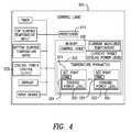
In the above exemplary embodiment, thesetpoints 223 utilize atemperature value 225 to construct thetemperature parameter 222 that defines a desired temperature trajectory of the modulated surface of thechamber walls 102 over the processing period. However, with reference toFIG. 4 , because there is a tight correlation between the power of the cooling system (i.e., the speed of theblower 140 and/or the setting of the coolant regulator131) and the radiance of theheating elements 114, as another embodiment it is equally possible to define thetemperature parameter 322 as having one ormore setpoints 323, each with an associatedtime value 324 and coolingpower level value 325. In this case, theprocessor 310 of the secondembodiment control logic 300 generates a current target coolingpower level 328 in a manner analogous to that used above to find thecurrent target temperature 228, and then sends signals to the coolingpower control output 333 to set the power of the cooling system (i.e.,blower 140 and/or coolant regulator131) to match the current target coolingpower level 328.
Because of the inherent consistency and reproducibility of processing runs, thetemperature parameter 322 defined as a series of coolingpower levels 325 at respective time values324 is functionally similar to thetemperature parameter 222 of the above embodiment. However, variations between the desired and actual temperatures of the modulated region of thechamber walls 102 may be greater than in the first embodiment.
Embodiments of the present invention provide for controlled modulation of theentire chamber wall 102, or a portion of thechamber wall 102, over the processing period. In particular, as indicated inFIG. 3 , the controlled modulation of thechamber wall 102 within individual steps of the film formation process can be achieved. For example, a higher overall growth rate with reduced faceting can be achieved by providing atemperature parameter top surface 105, and then slowly decreases thetop surface 105 temperature as the deposition or growth of the film on the substrate progresses. Selection of thetemperature parameter wall 102 temperature causes gas to crack or decompose better, thereby enhancing the growth rate. Film composition can be varied through this mechanism as well, since some dopant species absorb or incorporate better when decomposed. All of this may be done within a process step, as the film formation procedure goes through various stages. It will thus be understood that the skilled artisan can empirically determine and select thetemperature parameter
With reference toFIG. 5 andFIG. 6 , athird embodiment system 400 provides additional independent parameters for the film deposition process by allowing independent control of the temperatures of multiple portions of thechamber wall 102. For ease of presentation, components inFIG. 5 that are essentially identical to those in the prior embodiments have been provided the same reference numbers. As indicated in the discussion ofFIG. 1 , coolant enteringinlet port 124 passes across thetop surface 105 of thechamber walls 102, thus cooling thetop surface 105. Similarly, coolant entering thebottom inlet port 126 cools thebottom surface 107. Hence, by independently controlling the amount of coolant entering thetop inlet port 124 and thebottom inlet port 126 it is possible to respectively independently control the temperature of thetop surface 105 and thebottom surface 107 of thechamber walls 102. To effectuate this, this embodiment provides afirst coolant regulator 431 for controlling the rate of coolant flow into theupper inlet port 124, and asecond coolant regulator 439 for controlling the rate of coolant flow into thelower inlet port 126.
Thecoolant regulators respective chamber wall 102 surfaces, or the like. Alternatively, one of thecoolant regulators blower 140.
For example, with reference toFIG. 7 , thefirst temperature parameter 560 may have fifteensetpoints 563 defining afirst temperature trajectory 601, analogous to that depicted inFIG. 3 , for thetop surface 105 relative to the process temperature. For example, seven points611-617 may comprise apre-bake temperature trajectory 610 for thetop surface 105. Four points621-624 may comprise a filmdeposition temperature trajectory 620 for thetop surface 105 that increases during the film deposition step. This increase may be substantially asymptotic from the process temperature to a higher target temperature over the time period of the film deposition step. Such an increase in temperature of thetop surface 105 during the film deposition step yields higher deposition rates. Four points631-634 may comprise a cool-downtemperature trajectory 630 for thetop surface 105.
Thesecond temperature parameter 570 may also have, for example, eightsetpoints 573 defining asecond temperature trajectory 602 for thebottom surface 107 across the entire film formation process. Theprocessor 510 may utilize thefirst temperature parameter 560 to generate a firstcurrent target temperature 523, and utilize thesecond temperature parameter 570 to generate a secondcurrent target temperature 524. Monitoring of inputs, such as the topsurface temperature input 531, which receives first signals from the top surfacetemperature measuring device 132, enables theprocessor 510 to generate a currenttop surface temperature 521. Similarly, by monitoring the bottomsurface temperature input 532, which receives second signals from the bottom surfacetemperature measuring device 138, theprocessor 510 may generate a currentbottom surface temperature 522. Of course, the currenttop surface temperature 521, as well as the currentbottom surface temperature 522, may be a function of a plurality of inputs, as desired by the user.
Analogous to the previous embodiments, theprocessor 510 utilizes the firstcurrent target temperature 523 and the currenttop surface temperature 521 to send signals to the first coolingpower control output 533 to control thefirst coolant regulator 431, and hence to modulate thetop surface 105 temperature according to thefirst temperature parameter 560. Similarly, theprocessor 510 utilizes the secondcurrent target temperature 524 and the currentbottom surface temperature 522 to send signals to the second coolingpower control output 534 to control thesecond coolant regulator 439, and hence to modulate thebottom surface 107 temperature according to thefirst temperature parameter 560. Of course, thefirst temperature parameter 560 and thesecond temperature parameter 570 may be defined by respective cooling power levels rather than temperatures, as is done in the second embodiment, in which case it may not be necessary to monitor the currenttop surface temperature 521 or the currentbottom surface temperature 522 to control thefirst coolant regulator 431 and thesecond coolant regulator 439.
As shown inFIG. 8 , it is possible to use a firstvariable speed blower 701, and a secondvariable speed blower 702, to respectively control the temperature of thetop surface 105 andbottom surface 107 of thechamber walls 102. With further reference toFIG. 6 , thecontrol logic 500 is equally suited to control the embodiment depicted inFIG. 8 . First coolingpower control output 533 may control the speed offirst blower 701, while second coolingpower control output 534 may control the speed ofsecond blower 702.
With reference toFIG. 9 , it is possible to independently control the temperature of thetop surface 105 and thebottom surface 107 by changing the irradiancy bias betweentop lamps 802 andbottom lamps 804. Thetop lamps 802 are disposed above thetop surface 105 of thechamber walls 102, and thus heat thetop surface 105 while heating thesubstrate 106. Thebottom lamps 804 are disposed below thebottom surface 107 of thechamber walls 102, and thus heat thebottom surface 107 while heating thesubstrate 106. The combined irradiancy of thetop lamps 802 andbottom lamps 804 determines the final temperature of thesubstrate 106. If the irradiancy of thetop lamps 802 is increased while the irradiancy of thebottom lamps 804 is decreased, it is possible to increase the temperature of thetop surface 105 and decrease the temperature of thebottom surface 107, while keeping thesubstrate 106 at the same temperature. Reversing this irradiancy bias will lead to heating of thebottom surface 107 and cooling of thetop surface 105, while maintaining the temperature of thesubstrate 106. The irradiancy of thetop lamps 802 may therefore be controlled independent of the irradiancy of thebottom lamps 804. With reference toFIG. 6 , independent control of thetop lamps 802 andbottom lamps 804 permits thecontrol circuit 500 to control the irradiancy bias between thetop lamps 802 andbottom lamps 804. First coolingpower control output 533 may thus be used to control the speed ofvariable speed blower 140, while second coolingpower control output 534 may be used to control the irradiancy bias between thetop lamps 802 and thebottom lamps 804. It will be appreciated that second coolingpower control output 534 may actually be two independent outputs that respectively control the irradiancy of thetop lamps 802 and thebottom lamps 804, and the difference between these two irradiancy outputs yields the irradiancy bias that preferentially heats and cools one of thesurfaces other surface
For example, to cool thebottom surface 107, theprocessor 510 may control the second coolingpower control output 534 so that the irradiancy of thetop lamps 802 increases, while the irradiancy of thebottom lamps 804 decreases. From the temperature perspective of thesubstrate 106, little has changed. However, from the point of view of thebottom surface 107, as less radiant energy impinges upon thebottom surface 107, thebottom surface 107 will begin to cool. It will be appreciated that, since more radiant energy will impinge upon thetop surface 105, thetop surface 105 may begin to heat beyond itsfirst temperature parameter 560. In response to this, theprocessor 510 may control the first coolingpower control output 533 to increase the speed of thevariable speed blower 140 to cool thetop surface 105, which will incidentally lead to even more cooling of thebottom surface 107. Similarly, reversing the bias can lead to heating of thebottom surface 107. Hence, by using the second coolingpower control output 534 to modulate the irradiancy bias between thelamps bottom surface 107 with respect to thetop surface 105.
It is possible not only to temperature-modulate the top andbottom surfaces chamber walls 102, but also to modulate side portions of thechamber walls 102. For example, with reference toFIG. 1 , with suitable control of inlet and outlet ducting, it is possible to control the respective temperatures of left adjacenttop surface 151 and right adjacent top surface152. The adjacenttop surface 151,152 are adjacent to thetop surface 105, and hence adjacent to the top surface of thesubstrate 106. Similarly, it is possible to temperature-modulate left adjacentbottom surface 153 and rightadjacent bottom surface 154, which are adjacent to thebottom surface 107, and hence adjacent to the bottom surface of thesubstrate 106. The control logic may be easily expanded to accommodate as many temperature parameters as there are individual chamber wall surface portions to temperature-modulate, and the method of doing so should be clear in light of this disclosure.
Although the invention herein has been described with reference to particular embodiments, it is to be understood that these embodiments are merely illustrative of the principles and applications of the present invention. It will be apparent to those skilled in the art that various modifications and variations can be made to the method of the present invention without departing from the spirit and scope of the invention. Thus, it is intended that the present invention include modifications and variations that are within the scope of the appended claims and their equivalents.
Claims (16)
1. A film formation system comprising:
a chamber wall defining an inner volume of a chamber to accept a substrate on which a film is to be formed;
a first cooling system to cool only a first portion of the chamber wall, the first portion of the chamber wall above the inner volume;
a first regulator to control cooling power of the first cooling system;
a first lamp to heat the first portion of the chamber wall;
a second cooling system to cool only a second portion of the chamber wall, the second portion of the chamber wall below the inner volume;
a second regulator to control cooling power of the second cooling system;
a second lamp to heat the second portion of the chamber wall;
an entry port to permit gas to enter the chamber to form the film on the substrate;
a controller containing an input for flow rate of the gas, the controller controlling the first regulator and the second regulator, the controller comprising: a memory to store the gas flow rate, a first temperature parameter defining a desired target temperature trajectory of the first portion of the chamber wall over a processing period and a second temperature parameter defining a desired target temperature trajectory of the second portion of the chamber wall over the processing period, the processing period including a film formation step, the target temperature trajectory being a non-constant value over the processing period; a user input/output system to enter the first temperature parameter; and
a first output to control the first regulator to control the temperature of the first portion of the chamber walls during the processing period and a second output to control the second regulator to control the temperature of the second portion of the chamber walls during the processing period so that the temperature tracks the target temperature trajectory during film formation; and a processing circuit to send first signals to the first output and second signals to the second output over the processing period according to the first temperature parameter and to enhance growth rate of the film, the controller controlling an irradiancy bias between the first lamp and the second lamp to selectively heat the first wall relative to the second wall.
2. The system ofclaim 1 , wherein the first temperature parameter comprises a plurality of setpoints, each setpoint comprising a respective time within the processing period.
3. The system ofclaim 2 , wherein each setpoint further comprises a respective temperature.
4. The system ofclaim 2 , wherein each setpoint further comprises a respective cooling power level.
5. The system ofclaim 1 , further comprising a first temperature measurement device to measure the temperature of the first portion of the wall and a second temperature measurement device to measure the temperature of the second portion of the wall.
6. The system ofclaim 5 , wherein the controller further comprises a first temperature input signal correlated to the temperature of the first portion of the wall, the first temperature input signal generated by the first temperature measurement device and a second temperature input signal correlated to the temperature of the second portion of the wall, the second temperature input signal generated by the second temperature measurement device.
7. The system ofclaim 6 , wherein the first output is based on the first temperature input signal, the second temperature input signal or a function of the first temperature input signal and the second temperature input signal.
8. The system ofclaim 1 , wherein the controller further comprises a feedback loop to control the power level of the first cooling system to cause a current measure of the wall temperature to match the temperature trajectory as a function of time.
9. The system ofclaim 5 , wherein the temperature measurement devices are one or more of an optical pyrometer or a thermocouple.
10. The system ofclaim 1 , wherein the first cooling system includes one or more of an air vane, adjustable iris, valve and blower.
11. The system ofclaim 1 , wherein the first lamp and the second lamp collectively heat the substrate.
12. The system ofclaim 1 , further comprising a first temperature measurement device to measure the temperature of the first portion of the wall and a second temperature measurement device to measure the temperature of the second portion of the wall.
13. The system ofclaim 12 , wherein the temperature measurement devices are selected from the group consisting of optical pyrometers, thermocouples and combinations thereof.
14. The system ofclaim 1 , wherein one or more of the first cooling system and the second cooling system use a coolant selected from the group consisting of air, water, nitrogen, helium, argon, inert gas and combinations thereof.
15. The system ofclaim 1 , wherein the controller further comprises at least one feedback loop to control the power level of one or more of the first cooling system and the second cooling system to cause a current measure of the wall temperature to match the temperature trajectory as a function of time.
16. The system ofclaim 1 , wherein the first cooling system and the second cooling system include one or more of an air vane, adjustable iris, valve or blower.
Priority Applications (1)
| Application Number | Priority Date | Filing Date | Title |
|---|---|---|---|
| US12/394,203US8991332B2 (en) | 2005-08-17 | 2009-02-27 | Apparatus to control semiconductor film deposition characteristics |
Applications Claiming Priority (2)
| Application Number | Priority Date | Filing Date | Title |
|---|---|---|---|
| US11/205,647US7718225B2 (en) | 2005-08-17 | 2005-08-17 | Method to control semiconductor film deposition characteristics |
| US12/394,203US8991332B2 (en) | 2005-08-17 | 2009-02-27 | Apparatus to control semiconductor film deposition characteristics |
Related Parent Applications (1)
| Application Number | Title | Priority Date | Filing Date |
|---|---|---|---|
| US11/205,647DivisionUS7718225B2 (en) | 2005-08-17 | 2005-08-17 | Method to control semiconductor film deposition characteristics |
Publications (2)
| Publication Number | Publication Date |
|---|---|
| US20090211523A1 US20090211523A1 (en) | 2009-08-27 |
| US8991332B2true US8991332B2 (en) | 2015-03-31 |
Family
ID=37758095
Family Applications (2)
| Application Number | Title | Priority Date | Filing Date |
|---|---|---|---|
| US11/205,647Active2028-04-17US7718225B2 (en) | 2005-08-17 | 2005-08-17 | Method to control semiconductor film deposition characteristics |
| US12/394,203Active2028-12-30US8991332B2 (en) | 2005-08-17 | 2009-02-27 | Apparatus to control semiconductor film deposition characteristics |
Family Applications Before (1)
| Application Number | Title | Priority Date | Filing Date |
|---|---|---|---|
| US11/205,647Active2028-04-17US7718225B2 (en) | 2005-08-17 | 2005-08-17 | Method to control semiconductor film deposition characteristics |
Country Status (5)
| Country | Link |
|---|---|
| US (2) | US7718225B2 (en) |
| JP (1) | JP5329221B2 (en) |
| KR (2) | KR101014907B1 (en) |
| TW (1) | TWI358754B (en) |
| WO (1) | WO2007021692A2 (en) |
Families Citing this family (420)
| Publication number | Priority date | Publication date | Assignee | Title |
|---|---|---|---|---|
| US7718225B2 (en)* | 2005-08-17 | 2010-05-18 | Applied Materials, Inc. | Method to control semiconductor film deposition characteristics |
| US8986456B2 (en)* | 2006-10-10 | 2015-03-24 | Asm America, Inc. | Precursor delivery system |
| US8706314B2 (en)* | 2008-07-31 | 2014-04-22 | Oracle America, Inc. | Method and apparatus for regulating temperature in a computer system |
| US10378106B2 (en) | 2008-11-14 | 2019-08-13 | Asm Ip Holding B.V. | Method of forming insulation film by modified PEALD |
| US9394608B2 (en) | 2009-04-06 | 2016-07-19 | Asm America, Inc. | Semiconductor processing reactor and components thereof |
| US20100263588A1 (en)* | 2009-04-15 | 2010-10-21 | Gan Zhiyin | Methods and apparatus for epitaxial growth of semiconductor materials |
| US8877655B2 (en) | 2010-05-07 | 2014-11-04 | Asm America, Inc. | Systems and methods for thin-film deposition of metal oxides using excited nitrogen-oxygen species |
| US8802201B2 (en) | 2009-08-14 | 2014-08-12 | Asm America, Inc. | Systems and methods for thin-film deposition of metal oxides using excited nitrogen-oxygen species |
| US8883270B2 (en)* | 2009-08-14 | 2014-11-11 | Asm America, Inc. | Systems and methods for thin-film deposition of metal oxides using excited nitrogen—oxygen species |
| US9312155B2 (en) | 2011-06-06 | 2016-04-12 | Asm Japan K.K. | High-throughput semiconductor-processing apparatus equipped with multiple dual-chamber modules |
| US9793148B2 (en) | 2011-06-22 | 2017-10-17 | Asm Japan K.K. | Method for positioning wafers in multiple wafer transport |
| US10364496B2 (en) | 2011-06-27 | 2019-07-30 | Asm Ip Holding B.V. | Dual section module having shared and unshared mass flow controllers |
| US10854498B2 (en) | 2011-07-15 | 2020-12-01 | Asm Ip Holding B.V. | Wafer-supporting device and method for producing same |
| US20130023129A1 (en) | 2011-07-20 | 2013-01-24 | Asm America, Inc. | Pressure transmitter for a semiconductor processing environment |
| DE102011083245B4 (en)* | 2011-09-22 | 2019-04-25 | Siltronic Ag | Method and device for depositing an epitaxial layer of silicon on a semiconductor wafer of monocrystalline silicon by vapor deposition in a process chamber |
| US9096931B2 (en) | 2011-10-27 | 2015-08-04 | Asm America, Inc | Deposition valve assembly and method of heating the same |
| US9341296B2 (en) | 2011-10-27 | 2016-05-17 | Asm America, Inc. | Heater jacket for a fluid line |
| US9017481B1 (en) | 2011-10-28 | 2015-04-28 | Asm America, Inc. | Process feed management for semiconductor substrate processing |
| US9167625B2 (en) | 2011-11-23 | 2015-10-20 | Asm Ip Holding B.V. | Radiation shielding for a substrate holder |
| US9005539B2 (en) | 2011-11-23 | 2015-04-14 | Asm Ip Holding B.V. | Chamber sealing member |
| US9202727B2 (en) | 2012-03-02 | 2015-12-01 | ASM IP Holding | Susceptor heater shim |
| US8946830B2 (en) | 2012-04-04 | 2015-02-03 | Asm Ip Holdings B.V. | Metal oxide protective layer for a semiconductor device |
| TWI622664B (en) | 2012-05-02 | 2018-05-01 | Asm智慧財產控股公司 | Phase stable film, structure and device comprising the same, and method of forming same |
| US8728832B2 (en) | 2012-05-07 | 2014-05-20 | Asm Ip Holdings B.V. | Semiconductor device dielectric interface layer |
| US8933375B2 (en) | 2012-06-27 | 2015-01-13 | Asm Ip Holding B.V. | Susceptor heater and method of heating a substrate |
| US9558931B2 (en) | 2012-07-27 | 2017-01-31 | Asm Ip Holding B.V. | System and method for gas-phase sulfur passivation of a semiconductor surface |
| US9117866B2 (en) | 2012-07-31 | 2015-08-25 | Asm Ip Holding B.V. | Apparatus and method for calculating a wafer position in a processing chamber under process conditions |
| US9169975B2 (en) | 2012-08-28 | 2015-10-27 | Asm Ip Holding B.V. | Systems and methods for mass flow controller verification |
| US9659799B2 (en) | 2012-08-28 | 2017-05-23 | Asm Ip Holding B.V. | Systems and methods for dynamic semiconductor process scheduling |
| US9021985B2 (en) | 2012-09-12 | 2015-05-05 | Asm Ip Holdings B.V. | Process gas management for an inductively-coupled plasma deposition reactor |
| US9324811B2 (en) | 2012-09-26 | 2016-04-26 | Asm Ip Holding B.V. | Structures and devices including a tensile-stressed silicon arsenic layer and methods of forming same |
| US10714315B2 (en) | 2012-10-12 | 2020-07-14 | Asm Ip Holdings B.V. | Semiconductor reaction chamber showerhead |
| US9640416B2 (en) | 2012-12-26 | 2017-05-02 | Asm Ip Holding B.V. | Single-and dual-chamber module-attachable wafer-handling chamber |
| US8772055B1 (en) | 2013-01-16 | 2014-07-08 | Applied Materials, Inc. | Multizone control of lamps in a conical lamphead using pyrometers |
| US8894870B2 (en) | 2013-02-01 | 2014-11-25 | Asm Ip Holding B.V. | Multi-step method and apparatus for etching compounds containing a metal |
| US20160376700A1 (en) | 2013-02-01 | 2016-12-29 | Asm Ip Holding B.V. | System for treatment of deposition reactor |
| US9748121B2 (en)* | 2013-03-05 | 2017-08-29 | Applied Materials, Inc. | Thermal coupled quartz dome heat sink |
| US9484191B2 (en) | 2013-03-08 | 2016-11-01 | Asm Ip Holding B.V. | Pulsed remote plasma method and system |
| US9589770B2 (en) | 2013-03-08 | 2017-03-07 | Asm Ip Holding B.V. | Method and systems for in-situ formation of intermediate reactive species |
| US8993054B2 (en) | 2013-07-12 | 2015-03-31 | Asm Ip Holding B.V. | Method and system to reduce outgassing in a reaction chamber |
| US9018111B2 (en) | 2013-07-22 | 2015-04-28 | Asm Ip Holding B.V. | Semiconductor reaction chamber with plasma capabilities |
| US9396934B2 (en) | 2013-08-14 | 2016-07-19 | Asm Ip Holding B.V. | Methods of forming films including germanium tin and structures and devices including the films |
| US9793115B2 (en) | 2013-08-14 | 2017-10-17 | Asm Ip Holding B.V. | Structures and devices including germanium-tin films and methods of forming same |
| US9240412B2 (en) | 2013-09-27 | 2016-01-19 | Asm Ip Holding B.V. | Semiconductor structure and device and methods of forming same using selective epitaxial process |
| US9556516B2 (en) | 2013-10-09 | 2017-01-31 | ASM IP Holding B.V | Method for forming Ti-containing film by PEALD using TDMAT or TDEAT |
| US9605343B2 (en) | 2013-11-13 | 2017-03-28 | Asm Ip Holding B.V. | Method for forming conformal carbon films, structures conformal carbon film, and system of forming same |
| US10179947B2 (en) | 2013-11-26 | 2019-01-15 | Asm Ip Holding B.V. | Method for forming conformal nitrided, oxidized, or carbonized dielectric film by atomic layer deposition |
| US9338834B2 (en) | 2014-01-17 | 2016-05-10 | Taiwan Semiconductor Manufacturing Company Limited | Systems and methods for microwave-radiation annealing |
| US10683571B2 (en) | 2014-02-25 | 2020-06-16 | Asm Ip Holding B.V. | Gas supply manifold and method of supplying gases to chamber using same |
| US10167557B2 (en) | 2014-03-18 | 2019-01-01 | Asm Ip Holding B.V. | Gas distribution system, reactor including the system, and methods of using the same |
| US9447498B2 (en) | 2014-03-18 | 2016-09-20 | Asm Ip Holding B.V. | Method for performing uniform processing in gas system-sharing multiple reaction chambers |
| US11015245B2 (en) | 2014-03-19 | 2021-05-25 | Asm Ip Holding B.V. | Gas-phase reactor and system having exhaust plenum and components thereof |
| US9404587B2 (en) | 2014-04-24 | 2016-08-02 | ASM IP Holding B.V | Lockout tagout for semiconductor vacuum valve |
| US10858737B2 (en) | 2014-07-28 | 2020-12-08 | Asm Ip Holding B.V. | Showerhead assembly and components thereof |
| US9543180B2 (en) | 2014-08-01 | 2017-01-10 | Asm Ip Holding B.V. | Apparatus and method for transporting wafers between wafer carrier and process tool under vacuum |
| US9890456B2 (en) | 2014-08-21 | 2018-02-13 | Asm Ip Holding B.V. | Method and system for in situ formation of gas-phase compounds |
| US9657845B2 (en) | 2014-10-07 | 2017-05-23 | Asm Ip Holding B.V. | Variable conductance gas distribution apparatus and method |
| US10941490B2 (en) | 2014-10-07 | 2021-03-09 | Asm Ip Holding B.V. | Multiple temperature range susceptor, assembly, reactor and system including the susceptor, and methods of using the same |
| US10095114B2 (en) | 2014-11-14 | 2018-10-09 | Applied Materials, Inc. | Process chamber for field guided exposure and method for implementing the process chamber |
| KR102300403B1 (en) | 2014-11-19 | 2021-09-09 | 에이에스엠 아이피 홀딩 비.브이. | Method of depositing thin film |
| KR102263121B1 (en) | 2014-12-22 | 2021-06-09 | 에이에스엠 아이피 홀딩 비.브이. | Semiconductor device and manufacuring method thereof |
| US9478415B2 (en) | 2015-02-13 | 2016-10-25 | Asm Ip Holding B.V. | Method for forming film having low resistance and shallow junction depth |
| US10529542B2 (en) | 2015-03-11 | 2020-01-07 | Asm Ip Holdings B.V. | Cross-flow reactor and method |
| US10276355B2 (en) | 2015-03-12 | 2019-04-30 | Asm Ip Holding B.V. | Multi-zone reactor, system including the reactor, and method of using the same |
| US20160282886A1 (en)* | 2015-03-27 | 2016-09-29 | Applied Materials, Inc. | Upper dome temperature closed loop control |
| US9864276B2 (en) | 2015-04-07 | 2018-01-09 | Applied Materials, Inc. | Laser annealing and electric field |
| US10458018B2 (en) | 2015-06-26 | 2019-10-29 | Asm Ip Holding B.V. | Structures including metal carbide material, devices including the structures, and methods of forming same |
| US10600673B2 (en) | 2015-07-07 | 2020-03-24 | Asm Ip Holding B.V. | Magnetic susceptor to baseplate seal |
| US10043661B2 (en) | 2015-07-13 | 2018-08-07 | Asm Ip Holding B.V. | Method for protecting layer by forming hydrocarbon-based extremely thin film |
| US9899291B2 (en) | 2015-07-13 | 2018-02-20 | Asm Ip Holding B.V. | Method for protecting layer by forming hydrocarbon-based extremely thin film |
| US10083836B2 (en) | 2015-07-24 | 2018-09-25 | Asm Ip Holding B.V. | Formation of boron-doped titanium metal films with high work function |
| US10087525B2 (en) | 2015-08-04 | 2018-10-02 | Asm Ip Holding B.V. | Variable gap hard stop design |
| US9647114B2 (en) | 2015-08-14 | 2017-05-09 | Asm Ip Holding B.V. | Methods of forming highly p-type doped germanium tin films and structures and devices including the films |
| US9711345B2 (en) | 2015-08-25 | 2017-07-18 | Asm Ip Holding B.V. | Method for forming aluminum nitride-based film by PEALD |
| US9960072B2 (en) | 2015-09-29 | 2018-05-01 | Asm Ip Holding B.V. | Variable adjustment for precise matching of multiple chamber cavity housings |
| US9909214B2 (en) | 2015-10-15 | 2018-03-06 | Asm Ip Holding B.V. | Method for depositing dielectric film in trenches by PEALD |
| US10211308B2 (en) | 2015-10-21 | 2019-02-19 | Asm Ip Holding B.V. | NbMC layers |
| US10322384B2 (en) | 2015-11-09 | 2019-06-18 | Asm Ip Holding B.V. | Counter flow mixer for process chamber |
| US9455138B1 (en) | 2015-11-10 | 2016-09-27 | Asm Ip Holding B.V. | Method for forming dielectric film in trenches by PEALD using H-containing gas |
| US9905420B2 (en) | 2015-12-01 | 2018-02-27 | Asm Ip Holding B.V. | Methods of forming silicon germanium tin films and structures and devices including the films |
| US9607837B1 (en) | 2015-12-21 | 2017-03-28 | Asm Ip Holding B.V. | Method for forming silicon oxide cap layer for solid state diffusion process |
| US9627221B1 (en) | 2015-12-28 | 2017-04-18 | Asm Ip Holding B.V. | Continuous process incorporating atomic layer etching |
| US9735024B2 (en) | 2015-12-28 | 2017-08-15 | Asm Ip Holding B.V. | Method of atomic layer etching using functional group-containing fluorocarbon |
| US11139308B2 (en) | 2015-12-29 | 2021-10-05 | Asm Ip Holding B.V. | Atomic layer deposition of III-V compounds to form V-NAND devices |
| US20170207078A1 (en)* | 2016-01-15 | 2017-07-20 | Taiwan Semiconductor Manufacturing Co., Ltd. | Atomic layer deposition apparatus and semiconductor process |
| US10529554B2 (en) | 2016-02-19 | 2020-01-07 | Asm Ip Holding B.V. | Method for forming silicon nitride film selectively on sidewalls or flat surfaces of trenches |
| US10468251B2 (en) | 2016-02-19 | 2019-11-05 | Asm Ip Holding B.V. | Method for forming spacers using silicon nitride film for spacer-defined multiple patterning |
| US9754779B1 (en) | 2016-02-19 | 2017-09-05 | Asm Ip Holding B.V. | Method for forming silicon nitride film selectively on sidewalls or flat surfaces of trenches |
| US10501866B2 (en) | 2016-03-09 | 2019-12-10 | Asm Ip Holding B.V. | Gas distribution apparatus for improved film uniformity in an epitaxial system |
| US10343920B2 (en) | 2016-03-18 | 2019-07-09 | Asm Ip Holding B.V. | Aligned carbon nanotubes |
| US9892913B2 (en) | 2016-03-24 | 2018-02-13 | Asm Ip Holding B.V. | Radial and thickness control via biased multi-port injection settings |
| US10865475B2 (en) | 2016-04-21 | 2020-12-15 | Asm Ip Holding B.V. | Deposition of metal borides and silicides |
| US10087522B2 (en) | 2016-04-21 | 2018-10-02 | Asm Ip Holding B.V. | Deposition of metal borides |
| US10190213B2 (en) | 2016-04-21 | 2019-01-29 | Asm Ip Holding B.V. | Deposition of metal borides |
| US10032628B2 (en) | 2016-05-02 | 2018-07-24 | Asm Ip Holding B.V. | Source/drain performance through conformal solid state doping |
| US10367080B2 (en) | 2016-05-02 | 2019-07-30 | Asm Ip Holding B.V. | Method of forming a germanium oxynitride film |
| KR102592471B1 (en) | 2016-05-17 | 2023-10-20 | 에이에스엠 아이피 홀딩 비.브이. | Method of forming metal interconnection and method of fabricating semiconductor device using the same |
| US11453943B2 (en) | 2016-05-25 | 2022-09-27 | Asm Ip Holding B.V. | Method for forming carbon-containing silicon/metal oxide or nitride film by ALD using silicon precursor and hydrocarbon precursor |
| US10388509B2 (en) | 2016-06-28 | 2019-08-20 | Asm Ip Holding B.V. | Formation of epitaxial layers via dislocation filtering |
| US10612137B2 (en) | 2016-07-08 | 2020-04-07 | Asm Ip Holdings B.V. | Organic reactants for atomic layer deposition |
| US9859151B1 (en) | 2016-07-08 | 2018-01-02 | Asm Ip Holding B.V. | Selective film deposition method to form air gaps |
| US9793135B1 (en) | 2016-07-14 | 2017-10-17 | ASM IP Holding B.V | Method of cyclic dry etching using etchant film |
| US10714385B2 (en) | 2016-07-19 | 2020-07-14 | Asm Ip Holding B.V. | Selective deposition of tungsten |
| KR102354490B1 (en) | 2016-07-27 | 2022-01-21 | 에이에스엠 아이피 홀딩 비.브이. | Method of processing a substrate |
| US10177025B2 (en) | 2016-07-28 | 2019-01-08 | Asm Ip Holding B.V. | Method and apparatus for filling a gap |
| US9812320B1 (en) | 2016-07-28 | 2017-11-07 | Asm Ip Holding B.V. | Method and apparatus for filling a gap |
| KR102532607B1 (en) | 2016-07-28 | 2023-05-15 | 에이에스엠 아이피 홀딩 비.브이. | Substrate processing apparatus and method of operating the same |
| US10395919B2 (en) | 2016-07-28 | 2019-08-27 | Asm Ip Holding B.V. | Method and apparatus for filling a gap |
| US9887082B1 (en) | 2016-07-28 | 2018-02-06 | Asm Ip Holding B.V. | Method and apparatus for filling a gap |
| US10090316B2 (en) | 2016-09-01 | 2018-10-02 | Asm Ip Holding B.V. | 3D stacked multilayer semiconductor memory using doped select transistor channel |
| US10410943B2 (en) | 2016-10-13 | 2019-09-10 | Asm Ip Holding B.V. | Method for passivating a surface of a semiconductor and related systems |
| US10643826B2 (en) | 2016-10-26 | 2020-05-05 | Asm Ip Holdings B.V. | Methods for thermally calibrating reaction chambers |
| US11532757B2 (en) | 2016-10-27 | 2022-12-20 | Asm Ip Holding B.V. | Deposition of charge trapping layers |
| US10714350B2 (en) | 2016-11-01 | 2020-07-14 | ASM IP Holdings, B.V. | Methods for forming a transition metal niobium nitride film on a substrate by atomic layer deposition and related semiconductor device structures |
| US10435790B2 (en) | 2016-11-01 | 2019-10-08 | Asm Ip Holding B.V. | Method of subatmospheric plasma-enhanced ALD using capacitively coupled electrodes with narrow gap |
| US10229833B2 (en) | 2016-11-01 | 2019-03-12 | Asm Ip Holding B.V. | Methods for forming a transition metal nitride film on a substrate by atomic layer deposition and related semiconductor device structures |
| US10643904B2 (en) | 2016-11-01 | 2020-05-05 | Asm Ip Holdings B.V. | Methods for forming a semiconductor device and related semiconductor device structures |
| US10134757B2 (en) | 2016-11-07 | 2018-11-20 | Asm Ip Holding B.V. | Method of processing a substrate and a device manufactured by using the method |
| KR102546317B1 (en) | 2016-11-15 | 2023-06-21 | 에이에스엠 아이피 홀딩 비.브이. | Gas supply unit and substrate processing apparatus including the same |
| US10340135B2 (en) | 2016-11-28 | 2019-07-02 | Asm Ip Holding B.V. | Method of topologically restricted plasma-enhanced cyclic deposition of silicon or metal nitride |
| KR102762543B1 (en) | 2016-12-14 | 2025-02-05 | 에이에스엠 아이피 홀딩 비.브이. | Substrate processing apparatus |
| US9916980B1 (en) | 2016-12-15 | 2018-03-13 | Asm Ip Holding B.V. | Method of forming a structure on a substrate |
| US11581186B2 (en) | 2016-12-15 | 2023-02-14 | Asm Ip Holding B.V. | Sequential infiltration synthesis apparatus |
| US11447861B2 (en) | 2016-12-15 | 2022-09-20 | Asm Ip Holding B.V. | Sequential infiltration synthesis apparatus and a method of forming a patterned structure |
| KR102700194B1 (en) | 2016-12-19 | 2024-08-28 | 에이에스엠 아이피 홀딩 비.브이. | Substrate processing apparatus |
| US10269558B2 (en) | 2016-12-22 | 2019-04-23 | Asm Ip Holding B.V. | Method of forming a structure on a substrate |
| US10867788B2 (en) | 2016-12-28 | 2020-12-15 | Asm Ip Holding B.V. | Method of forming a structure on a substrate |
| US11390950B2 (en) | 2017-01-10 | 2022-07-19 | Asm Ip Holding B.V. | Reactor system and method to reduce residue buildup during a film deposition process |
| US10655221B2 (en) | 2017-02-09 | 2020-05-19 | Asm Ip Holding B.V. | Method for depositing oxide film by thermal ALD and PEALD |
| US10468261B2 (en) | 2017-02-15 | 2019-11-05 | Asm Ip Holding B.V. | Methods for forming a metallic film on a substrate by cyclical deposition and related semiconductor device structures |
| US10529563B2 (en) | 2017-03-29 | 2020-01-07 | Asm Ip Holdings B.V. | Method for forming doped metal oxide films on a substrate by cyclical deposition and related semiconductor device structures |
| US10283353B2 (en) | 2017-03-29 | 2019-05-07 | Asm Ip Holding B.V. | Method of reforming insulating film deposited on substrate with recess pattern |
| US10103040B1 (en) | 2017-03-31 | 2018-10-16 | Asm Ip Holding B.V. | Apparatus and method for manufacturing a semiconductor device |
| USD830981S1 (en) | 2017-04-07 | 2018-10-16 | Asm Ip Holding B.V. | Susceptor for semiconductor substrate processing apparatus |
| KR102457289B1 (en) | 2017-04-25 | 2022-10-21 | 에이에스엠 아이피 홀딩 비.브이. | Method for depositing a thin film and manufacturing a semiconductor device |
| US10892156B2 (en) | 2017-05-08 | 2021-01-12 | Asm Ip Holding B.V. | Methods for forming a silicon nitride film on a substrate and related semiconductor device structures |
| US10446393B2 (en) | 2017-05-08 | 2019-10-15 | Asm Ip Holding B.V. | Methods for forming silicon-containing epitaxial layers and related semiconductor device structures |
| US10770286B2 (en) | 2017-05-08 | 2020-09-08 | Asm Ip Holdings B.V. | Methods for selectively forming a silicon nitride film on a substrate and related semiconductor device structures |
| US10504742B2 (en) | 2017-05-31 | 2019-12-10 | Asm Ip Holding B.V. | Method of atomic layer etching using hydrogen plasma |
| US10886123B2 (en) | 2017-06-02 | 2021-01-05 | Asm Ip Holding B.V. | Methods for forming low temperature semiconductor layers and related semiconductor device structures |
| US12040200B2 (en) | 2017-06-20 | 2024-07-16 | Asm Ip Holding B.V. | Semiconductor processing apparatus and methods for calibrating a semiconductor processing apparatus |
| US11306395B2 (en) | 2017-06-28 | 2022-04-19 | Asm Ip Holding B.V. | Methods for depositing a transition metal nitride film on a substrate by atomic layer deposition and related deposition apparatus |
| US10685834B2 (en) | 2017-07-05 | 2020-06-16 | Asm Ip Holdings B.V. | Methods for forming a silicon germanium tin layer and related semiconductor device structures |
| KR20190009245A (en) | 2017-07-18 | 2019-01-28 | 에이에스엠 아이피 홀딩 비.브이. | Methods for forming a semiconductor device structure and related semiconductor device structures |
| US11018002B2 (en) | 2017-07-19 | 2021-05-25 | Asm Ip Holding B.V. | Method for selectively depositing a Group IV semiconductor and related semiconductor device structures |
| US11374112B2 (en) | 2017-07-19 | 2022-06-28 | Asm Ip Holding B.V. | Method for depositing a group IV semiconductor and related semiconductor device structures |
| US10541333B2 (en) | 2017-07-19 | 2020-01-21 | Asm Ip Holding B.V. | Method for depositing a group IV semiconductor and related semiconductor device structures |
| US10312055B2 (en) | 2017-07-26 | 2019-06-04 | Asm Ip Holding B.V. | Method of depositing film by PEALD using negative bias |
| US10590535B2 (en) | 2017-07-26 | 2020-03-17 | Asm Ip Holdings B.V. | Chemical treatment, deposition and/or infiltration apparatus and method for using the same |
| US10605530B2 (en) | 2017-07-26 | 2020-03-31 | Asm Ip Holding B.V. | Assembly of a liner and a flange for a vertical furnace as well as the liner and the vertical furnace |
| TWI815813B (en) | 2017-08-04 | 2023-09-21 | 荷蘭商Asm智慧財產控股公司 | Showerhead assembly for distributing a gas within a reaction chamber |
| US10692741B2 (en) | 2017-08-08 | 2020-06-23 | Asm Ip Holdings B.V. | Radiation shield |
| US10770336B2 (en) | 2017-08-08 | 2020-09-08 | Asm Ip Holding B.V. | Substrate lift mechanism and reactor including same |
| US11139191B2 (en) | 2017-08-09 | 2021-10-05 | Asm Ip Holding B.V. | Storage apparatus for storing cassettes for substrates and processing apparatus equipped therewith |
| US11769682B2 (en) | 2017-08-09 | 2023-09-26 | Asm Ip Holding B.V. | Storage apparatus for storing cassettes for substrates and processing apparatus equipped therewith |
| US10249524B2 (en) | 2017-08-09 | 2019-04-02 | Asm Ip Holding B.V. | Cassette holder assembly for a substrate cassette and holding member for use in such assembly |
| US10236177B1 (en) | 2017-08-22 | 2019-03-19 | ASM IP Holding B.V.. | Methods for depositing a doped germanium tin semiconductor and related semiconductor device structures |
| USD900036S1 (en) | 2017-08-24 | 2020-10-27 | Asm Ip Holding B.V. | Heater electrical connector and adapter |
| US11830730B2 (en) | 2017-08-29 | 2023-11-28 | Asm Ip Holding B.V. | Layer forming method and apparatus |
| KR102491945B1 (en) | 2017-08-30 | 2023-01-26 | 에이에스엠 아이피 홀딩 비.브이. | Substrate processing apparatus |
| US11295980B2 (en) | 2017-08-30 | 2022-04-05 | Asm Ip Holding B.V. | Methods for depositing a molybdenum metal film over a dielectric surface of a substrate by a cyclical deposition process and related semiconductor device structures |
| US11056344B2 (en) | 2017-08-30 | 2021-07-06 | Asm Ip Holding B.V. | Layer forming method |
| KR102401446B1 (en) | 2017-08-31 | 2022-05-24 | 에이에스엠 아이피 홀딩 비.브이. | Substrate processing apparatus |
| US10607895B2 (en) | 2017-09-18 | 2020-03-31 | Asm Ip Holdings B.V. | Method for forming a semiconductor device structure comprising a gate fill metal |
| KR102630301B1 (en) | 2017-09-21 | 2024-01-29 | 에이에스엠 아이피 홀딩 비.브이. | Method of sequential infiltration synthesis treatment of infiltrateable material and structures and devices formed using same |
| US10844484B2 (en) | 2017-09-22 | 2020-11-24 | Asm Ip Holding B.V. | Apparatus for dispensing a vapor phase reactant to a reaction chamber and related methods |
| US10658205B2 (en) | 2017-09-28 | 2020-05-19 | Asm Ip Holdings B.V. | Chemical dispensing apparatus and methods for dispensing a chemical to a reaction chamber |
| US10403504B2 (en) | 2017-10-05 | 2019-09-03 | Asm Ip Holding B.V. | Method for selectively depositing a metallic film on a substrate |
| US10319588B2 (en) | 2017-10-10 | 2019-06-11 | Asm Ip Holding B.V. | Method for depositing a metal chalcogenide on a substrate by cyclical deposition |
| US10923344B2 (en) | 2017-10-30 | 2021-02-16 | Asm Ip Holding B.V. | Methods for forming a semiconductor structure and related semiconductor structures |
| KR102443047B1 (en) | 2017-11-16 | 2022-09-14 | 에이에스엠 아이피 홀딩 비.브이. | Method of processing a substrate and a device manufactured by the same |
| US10910262B2 (en) | 2017-11-16 | 2021-02-02 | Asm Ip Holding B.V. | Method of selectively depositing a capping layer structure on a semiconductor device structure |
| US11022879B2 (en) | 2017-11-24 | 2021-06-01 | Asm Ip Holding B.V. | Method of forming an enhanced unexposed photoresist layer |
| WO2019103613A1 (en) | 2017-11-27 | 2019-05-31 | Asm Ip Holding B.V. | A storage device for storing wafer cassettes for use with a batch furnace |
| CN111344522B (en) | 2017-11-27 | 2022-04-12 | 阿斯莫Ip控股公司 | Including clean mini-environment device |
| US10290508B1 (en) | 2017-12-05 | 2019-05-14 | Asm Ip Holding B.V. | Method for forming vertical spacers for spacer-defined patterning |
| US10872771B2 (en) | 2018-01-16 | 2020-12-22 | Asm Ip Holding B. V. | Method for depositing a material film on a substrate within a reaction chamber by a cyclical deposition process and related device structures |
| KR102695659B1 (en) | 2018-01-19 | 2024-08-14 | 에이에스엠 아이피 홀딩 비.브이. | Method for depositing a gap filling layer by plasma assisted deposition |
| TWI799494B (en) | 2018-01-19 | 2023-04-21 | 荷蘭商Asm 智慧財產控股公司 | Deposition method |
| USD903477S1 (en) | 2018-01-24 | 2020-12-01 | Asm Ip Holdings B.V. | Metal clamp |
| US11018047B2 (en) | 2018-01-25 | 2021-05-25 | Asm Ip Holding B.V. | Hybrid lift pin |
| USD880437S1 (en) | 2018-02-01 | 2020-04-07 | Asm Ip Holding B.V. | Gas supply plate for semiconductor manufacturing apparatus |
| US10535516B2 (en) | 2018-02-01 | 2020-01-14 | Asm Ip Holdings B.V. | Method for depositing a semiconductor structure on a surface of a substrate and related semiconductor structures |
| US11081345B2 (en) | 2018-02-06 | 2021-08-03 | Asm Ip Holding B.V. | Method of post-deposition treatment for silicon oxide film |
| WO2019158960A1 (en) | 2018-02-14 | 2019-08-22 | Asm Ip Holding B.V. | A method for depositing a ruthenium-containing film on a substrate by a cyclical deposition process |
| US10896820B2 (en) | 2018-02-14 | 2021-01-19 | Asm Ip Holding B.V. | Method for depositing a ruthenium-containing film on a substrate by a cyclical deposition process |
| US10731249B2 (en) | 2018-02-15 | 2020-08-04 | Asm Ip Holding B.V. | Method of forming a transition metal containing film on a substrate by a cyclical deposition process, a method for supplying a transition metal halide compound to a reaction chamber, and related vapor deposition apparatus |
| US10658181B2 (en) | 2018-02-20 | 2020-05-19 | Asm Ip Holding B.V. | Method of spacer-defined direct patterning in semiconductor fabrication |
| KR102636427B1 (en) | 2018-02-20 | 2024-02-13 | 에이에스엠 아이피 홀딩 비.브이. | Substrate processing method and apparatus |
| US10975470B2 (en) | 2018-02-23 | 2021-04-13 | Asm Ip Holding B.V. | Apparatus for detecting or monitoring for a chemical precursor in a high temperature environment |
| US11473195B2 (en) | 2018-03-01 | 2022-10-18 | Asm Ip Holding B.V. | Semiconductor processing apparatus and a method for processing a substrate |
| US11629406B2 (en) | 2018-03-09 | 2023-04-18 | Asm Ip Holding B.V. | Semiconductor processing apparatus comprising one or more pyrometers for measuring a temperature of a substrate during transfer of the substrate |
| US11114283B2 (en) | 2018-03-16 | 2021-09-07 | Asm Ip Holding B.V. | Reactor, system including the reactor, and methods of manufacturing and using same |
| KR102646467B1 (en) | 2018-03-27 | 2024-03-11 | 에이에스엠 아이피 홀딩 비.브이. | Method of forming an electrode on a substrate and a semiconductor device structure including an electrode |
| US11230766B2 (en) | 2018-03-29 | 2022-01-25 | Asm Ip Holding B.V. | Substrate processing apparatus and method |
| US10510536B2 (en) | 2018-03-29 | 2019-12-17 | Asm Ip Holding B.V. | Method of depositing a co-doped polysilicon film on a surface of a substrate within a reaction chamber |
| US11088002B2 (en) | 2018-03-29 | 2021-08-10 | Asm Ip Holding B.V. | Substrate rack and a substrate processing system and method |
| KR102501472B1 (en) | 2018-03-30 | 2023-02-20 | 에이에스엠 아이피 홀딩 비.브이. | Substrate processing method |
| KR102600229B1 (en) | 2018-04-09 | 2023-11-10 | 에이에스엠 아이피 홀딩 비.브이. | Substrate supporting device, substrate processing apparatus including the same and substrate processing method |
| US12025484B2 (en) | 2018-05-08 | 2024-07-02 | Asm Ip Holding B.V. | Thin film forming method |
| TWI811348B (en) | 2018-05-08 | 2023-08-11 | 荷蘭商Asm 智慧財產控股公司 | Methods for depositing an oxide film on a substrate by a cyclical deposition process and related device structures |
| US12272527B2 (en) | 2018-05-09 | 2025-04-08 | Asm Ip Holding B.V. | Apparatus for use with hydrogen radicals and method of using same |
| KR20190129718A (en) | 2018-05-11 | 2019-11-20 | 에이에스엠 아이피 홀딩 비.브이. | Methods for forming a doped metal carbide film on a substrate and related semiconductor device structures |
| KR102596988B1 (en) | 2018-05-28 | 2023-10-31 | 에이에스엠 아이피 홀딩 비.브이. | Method of processing a substrate and a device manufactured by the same |
| TWI840362B (en) | 2018-06-04 | 2024-05-01 | 荷蘭商Asm Ip私人控股有限公司 | Wafer handling chamber with moisture reduction |
| US11718913B2 (en) | 2018-06-04 | 2023-08-08 | Asm Ip Holding B.V. | Gas distribution system and reactor system including same |
| US11286562B2 (en) | 2018-06-08 | 2022-03-29 | Asm Ip Holding B.V. | Gas-phase chemical reactor and method of using same |
| KR102568797B1 (en) | 2018-06-21 | 2023-08-21 | 에이에스엠 아이피 홀딩 비.브이. | Substrate processing system |
| US10797133B2 (en) | 2018-06-21 | 2020-10-06 | Asm Ip Holding B.V. | Method for depositing a phosphorus doped silicon arsenide film and related semiconductor device structures |
| KR102854019B1 (en) | 2018-06-27 | 2025-09-02 | 에이에스엠 아이피 홀딩 비.브이. | Periodic deposition method for forming a metal-containing material and films and structures comprising the metal-containing material |
| TWI873894B (en) | 2018-06-27 | 2025-02-21 | 荷蘭商Asm Ip私人控股有限公司 | Cyclic deposition methods for forming metal-containing material and films and structures including the metal-containing material |
| US10612136B2 (en) | 2018-06-29 | 2020-04-07 | ASM IP Holding, B.V. | Temperature-controlled flange and reactor system including same |
| KR102686758B1 (en) | 2018-06-29 | 2024-07-18 | 에이에스엠 아이피 홀딩 비.브이. | Method for depositing a thin film and manufacturing a semiconductor device |
| US10388513B1 (en) | 2018-07-03 | 2019-08-20 | Asm Ip Holding B.V. | Method for depositing silicon-free carbon-containing film as gap-fill layer by pulse plasma-assisted deposition |
| US10755922B2 (en) | 2018-07-03 | 2020-08-25 | Asm Ip Holding B.V. | Method for depositing silicon-free carbon-containing film as gap-fill layer by pulse plasma-assisted deposition |
| US10767789B2 (en) | 2018-07-16 | 2020-09-08 | Asm Ip Holding B.V. | Diaphragm valves, valve components, and methods for forming valve components |
| US10483099B1 (en) | 2018-07-26 | 2019-11-19 | Asm Ip Holding B.V. | Method for forming thermally stable organosilicon polymer film |
| US11053591B2 (en) | 2018-08-06 | 2021-07-06 | Asm Ip Holding B.V. | Multi-port gas injection system and reactor system including same |
| US10883175B2 (en) | 2018-08-09 | 2021-01-05 | Asm Ip Holding B.V. | Vertical furnace for processing substrates and a liner for use therein |
| US10829852B2 (en) | 2018-08-16 | 2020-11-10 | Asm Ip Holding B.V. | Gas distribution device for a wafer processing apparatus |
| US11430674B2 (en) | 2018-08-22 | 2022-08-30 | Asm Ip Holding B.V. | Sensor array, apparatus for dispensing a vapor phase reactant to a reaction chamber and related methods |
| US11024523B2 (en) | 2018-09-11 | 2021-06-01 | Asm Ip Holding B.V. | Substrate processing apparatus and method |
| KR102707956B1 (en) | 2018-09-11 | 2024-09-19 | 에이에스엠 아이피 홀딩 비.브이. | Method for deposition of a thin film |
| US11049751B2 (en) | 2018-09-14 | 2021-06-29 | Asm Ip Holding B.V. | Cassette supply system to store and handle cassettes and processing apparatus equipped therewith |
| CN110970344B (en) | 2018-10-01 | 2024-10-25 | Asmip控股有限公司 | Substrate holding apparatus, system comprising the same and method of using the same |
| US11232963B2 (en) | 2018-10-03 | 2022-01-25 | Asm Ip Holding B.V. | Substrate processing apparatus and method |
| KR102592699B1 (en) | 2018-10-08 | 2023-10-23 | 에이에스엠 아이피 홀딩 비.브이. | Substrate support unit and apparatuses for depositing thin film and processing the substrate including the same |
| US10847365B2 (en) | 2018-10-11 | 2020-11-24 | Asm Ip Holding B.V. | Method of forming conformal silicon carbide film by cyclic CVD |
| US10811256B2 (en) | 2018-10-16 | 2020-10-20 | Asm Ip Holding B.V. | Method for etching a carbon-containing feature |
| KR102605121B1 (en) | 2018-10-19 | 2023-11-23 | 에이에스엠 아이피 홀딩 비.브이. | Substrate processing apparatus and substrate processing method |
| KR102546322B1 (en) | 2018-10-19 | 2023-06-21 | 에이에스엠 아이피 홀딩 비.브이. | Substrate processing apparatus and substrate processing method |
| USD948463S1 (en) | 2018-10-24 | 2022-04-12 | Asm Ip Holding B.V. | Susceptor for semiconductor substrate supporting apparatus |
| US10381219B1 (en) | 2018-10-25 | 2019-08-13 | Asm Ip Holding B.V. | Methods for forming a silicon nitride film |
| US12378665B2 (en) | 2018-10-26 | 2025-08-05 | Asm Ip Holding B.V. | High temperature coatings for a preclean and etch apparatus and related methods |
| US11087997B2 (en) | 2018-10-31 | 2021-08-10 | Asm Ip Holding B.V. | Substrate processing apparatus for processing substrates |
| KR102748291B1 (en) | 2018-11-02 | 2024-12-31 | 에이에스엠 아이피 홀딩 비.브이. | Substrate support unit and substrate processing apparatus including the same |
| US11572620B2 (en) | 2018-11-06 | 2023-02-07 | Asm Ip Holding B.V. | Methods for selectively depositing an amorphous silicon film on a substrate |
| US11031242B2 (en) | 2018-11-07 | 2021-06-08 | Asm Ip Holding B.V. | Methods for depositing a boron doped silicon germanium film |
| US10847366B2 (en) | 2018-11-16 | 2020-11-24 | Asm Ip Holding B.V. | Methods for depositing a transition metal chalcogenide film on a substrate by a cyclical deposition process |
| US10818758B2 (en) | 2018-11-16 | 2020-10-27 | Asm Ip Holding B.V. | Methods for forming a metal silicate film on a substrate in a reaction chamber and related semiconductor device structures |
| US10559458B1 (en) | 2018-11-26 | 2020-02-11 | Asm Ip Holding B.V. | Method of forming oxynitride film |
| US12040199B2 (en) | 2018-11-28 | 2024-07-16 | Asm Ip Holding B.V. | Substrate processing apparatus for processing substrates |
| US11217444B2 (en) | 2018-11-30 | 2022-01-04 | Asm Ip Holding B.V. | Method for forming an ultraviolet radiation responsive metal oxide-containing film |
| KR102636428B1 (en) | 2018-12-04 | 2024-02-13 | 에이에스엠 아이피 홀딩 비.브이. | A method for cleaning a substrate processing apparatus |
| US11158513B2 (en) | 2018-12-13 | 2021-10-26 | Asm Ip Holding B.V. | Methods for forming a rhenium-containing film on a substrate by a cyclical deposition process and related semiconductor device structures |
| TWI874340B (en) | 2018-12-14 | 2025-03-01 | 荷蘭商Asm Ip私人控股有限公司 | Method of forming device structure, structure formed by the method and system for performing the method |
| TWI866480B (en) | 2019-01-17 | 2024-12-11 | 荷蘭商Asm Ip 私人控股有限公司 | Methods of forming a transition metal containing film on a substrate by a cyclical deposition process |
| KR20210096302A (en) | 2019-01-18 | 2021-08-04 | 어플라이드 머티어리얼스, 인코포레이티드 | Film Structure for Electric Field Induced Photoresist Patterning Process |
| KR102727227B1 (en) | 2019-01-22 | 2024-11-07 | 에이에스엠 아이피 홀딩 비.브이. | Semiconductor processing device |
| CN111524788B (en) | 2019-02-01 | 2023-11-24 | Asm Ip私人控股有限公司 | Method for forming topologically selective films of silicon oxide |
| KR102626263B1 (en) | 2019-02-20 | 2024-01-16 | 에이에스엠 아이피 홀딩 비.브이. | Cyclical deposition method including treatment step and apparatus for same |
| TWI845607B (en) | 2019-02-20 | 2024-06-21 | 荷蘭商Asm Ip私人控股有限公司 | Cyclical deposition method and apparatus for filling a recess formed within a substrate surface |
| TWI838458B (en) | 2019-02-20 | 2024-04-11 | 荷蘭商Asm Ip私人控股有限公司 | Apparatus and methods for plug fill deposition in 3-d nand applications |
| TWI873122B (en) | 2019-02-20 | 2025-02-21 | 荷蘭商Asm Ip私人控股有限公司 | Method of filling a recess formed within a surface of a substrate, semiconductor structure formed according to the method, and semiconductor processing apparatus |
| TWI842826B (en) | 2019-02-22 | 2024-05-21 | 荷蘭商Asm Ip私人控股有限公司 | Substrate processing apparatus and method for processing substrate |
| US11742198B2 (en) | 2019-03-08 | 2023-08-29 | Asm Ip Holding B.V. | Structure including SiOCN layer and method of forming same |
| KR102782593B1 (en) | 2019-03-08 | 2025-03-14 | 에이에스엠 아이피 홀딩 비.브이. | Structure Including SiOC Layer and Method of Forming Same |
| KR102858005B1 (en) | 2019-03-08 | 2025-09-09 | 에이에스엠 아이피 홀딩 비.브이. | Method for Selective Deposition of Silicon Nitride Layer and Structure Including Selectively-Deposited Silicon Nitride Layer |
| JP2020167398A (en) | 2019-03-28 | 2020-10-08 | エーエスエム・アイピー・ホールディング・ベー・フェー | Door openers and substrate processing equipment provided with door openers |
| KR102809999B1 (en) | 2019-04-01 | 2025-05-19 | 에이에스엠 아이피 홀딩 비.브이. | Method of manufacturing semiconductor device |
| KR20200123380A (en) | 2019-04-19 | 2020-10-29 | 에이에스엠 아이피 홀딩 비.브이. | Layer forming method and apparatus |
| KR20200125453A (en) | 2019-04-24 | 2020-11-04 | 에이에스엠 아이피 홀딩 비.브이. | Gas-phase reactor system and method of using same |
| KR20200130121A (en) | 2019-05-07 | 2020-11-18 | 에이에스엠 아이피 홀딩 비.브이. | Chemical source vessel with dip tube |
| US11289326B2 (en) | 2019-05-07 | 2022-03-29 | Asm Ip Holding B.V. | Method for reforming amorphous carbon polymer film |
| KR20200130652A (en) | 2019-05-10 | 2020-11-19 | 에이에스엠 아이피 홀딩 비.브이. | Method of depositing material onto a surface and structure formed according to the method |
| JP7612342B2 (en) | 2019-05-16 | 2025-01-14 | エーエスエム・アイピー・ホールディング・ベー・フェー | Wafer boat handling apparatus, vertical batch furnace and method |
| JP7598201B2 (en) | 2019-05-16 | 2024-12-11 | エーエスエム・アイピー・ホールディング・ベー・フェー | Wafer boat handling apparatus, vertical batch furnace and method |
| USD947913S1 (en) | 2019-05-17 | 2022-04-05 | Asm Ip Holding B.V. | Susceptor shaft |
| USD975665S1 (en) | 2019-05-17 | 2023-01-17 | Asm Ip Holding B.V. | Susceptor shaft |
| USD935572S1 (en) | 2019-05-24 | 2021-11-09 | Asm Ip Holding B.V. | Gas channel plate |
| USD922229S1 (en) | 2019-06-05 | 2021-06-15 | Asm Ip Holding B.V. | Device for controlling a temperature of a gas supply unit |
| KR20200141002A (en) | 2019-06-06 | 2020-12-17 | 에이에스엠 아이피 홀딩 비.브이. | Method of using a gas-phase reactor system including analyzing exhausted gas |
| KR20200141931A (en) | 2019-06-10 | 2020-12-21 | 에이에스엠 아이피 홀딩 비.브이. | Method for cleaning quartz epitaxial chambers |
| KR20200143254A (en) | 2019-06-11 | 2020-12-23 | 에이에스엠 아이피 홀딩 비.브이. | Method of forming an electronic structure using an reforming gas, system for performing the method, and structure formed using the method |
| USD944946S1 (en) | 2019-06-14 | 2022-03-01 | Asm Ip Holding B.V. | Shower plate |
| USD931978S1 (en) | 2019-06-27 | 2021-09-28 | Asm Ip Holding B.V. | Showerhead vacuum transport |
| KR20210005515A (en) | 2019-07-03 | 2021-01-14 | 에이에스엠 아이피 홀딩 비.브이. | Temperature control assembly for substrate processing apparatus and method of using same |
| JP7499079B2 (en) | 2019-07-09 | 2024-06-13 | エーエスエム・アイピー・ホールディング・ベー・フェー | Plasma device using coaxial waveguide and substrate processing method |
| CN112216646A (en) | 2019-07-10 | 2021-01-12 | Asm Ip私人控股有限公司 | Substrate supporting assembly and substrate processing device comprising same |
| KR20210010307A (en) | 2019-07-16 | 2021-01-27 | 에이에스엠 아이피 홀딩 비.브이. | Substrate processing apparatus |
| KR102860110B1 (en) | 2019-07-17 | 2025-09-16 | 에이에스엠 아이피 홀딩 비.브이. | Methods of forming silicon germanium structures |
| KR20210010816A (en) | 2019-07-17 | 2021-01-28 | 에이에스엠 아이피 홀딩 비.브이. | Radical assist ignition plasma system and method |
| US11643724B2 (en) | 2019-07-18 | 2023-05-09 | Asm Ip Holding B.V. | Method of forming structures using a neutral beam |
| TWI839544B (en) | 2019-07-19 | 2024-04-21 | 荷蘭商Asm Ip私人控股有限公司 | Method of forming topology-controlled amorphous carbon polymer film |
| KR20210010817A (en) | 2019-07-19 | 2021-01-28 | 에이에스엠 아이피 홀딩 비.브이. | Method of Forming Topology-Controlled Amorphous Carbon Polymer Film |
| TWI851767B (en) | 2019-07-29 | 2024-08-11 | 荷蘭商Asm Ip私人控股有限公司 | Methods for selective deposition utilizing n-type dopants and/or alternative dopants to achieve high dopant incorporation |
| CN112309899A (en) | 2019-07-30 | 2021-02-02 | Asm Ip私人控股有限公司 | Substrate processing apparatus |
| CN112309900A (en) | 2019-07-30 | 2021-02-02 | Asm Ip私人控股有限公司 | Substrate processing apparatus |
| US12169361B2 (en) | 2019-07-30 | 2024-12-17 | Asm Ip Holding B.V. | Substrate processing apparatus and method |
| US11587815B2 (en) | 2019-07-31 | 2023-02-21 | Asm Ip Holding B.V. | Vertical batch furnace assembly |
| US11587814B2 (en) | 2019-07-31 | 2023-02-21 | Asm Ip Holding B.V. | Vertical batch furnace assembly |
| US11227782B2 (en) | 2019-07-31 | 2022-01-18 | Asm Ip Holding B.V. | Vertical batch furnace assembly |
| CN112323048B (en) | 2019-08-05 | 2024-02-09 | Asm Ip私人控股有限公司 | Liquid level sensor for chemical source container |
| CN112342526A (en) | 2019-08-09 | 2021-02-09 | Asm Ip私人控股有限公司 | Heater assembly including cooling device and method of using same |
| USD965044S1 (en) | 2019-08-19 | 2022-09-27 | Asm Ip Holding B.V. | Susceptor shaft |
| USD965524S1 (en) | 2019-08-19 | 2022-10-04 | Asm Ip Holding B.V. | Susceptor support |
| JP2021031769A (en) | 2019-08-21 | 2021-03-01 | エーエスエム アイピー ホールディング ビー.ブイ. | Production apparatus of mixed gas of film deposition raw material and film deposition apparatus |
| USD930782S1 (en) | 2019-08-22 | 2021-09-14 | Asm Ip Holding B.V. | Gas distributor |
| USD979506S1 (en) | 2019-08-22 | 2023-02-28 | Asm Ip Holding B.V. | Insulator |
| KR20210024423A (en) | 2019-08-22 | 2021-03-05 | 에이에스엠 아이피 홀딩 비.브이. | Method for forming a structure with a hole |
| USD940837S1 (en) | 2019-08-22 | 2022-01-11 | Asm Ip Holding B.V. | Electrode |
| USD949319S1 (en) | 2019-08-22 | 2022-04-19 | Asm Ip Holding B.V. | Exhaust duct |
| KR20210024420A (en) | 2019-08-23 | 2021-03-05 | 에이에스엠 아이피 홀딩 비.브이. | Method for depositing silicon oxide film having improved quality by peald using bis(diethylamino)silane |
| US11286558B2 (en) | 2019-08-23 | 2022-03-29 | Asm Ip Holding B.V. | Methods for depositing a molybdenum nitride film on a surface of a substrate by a cyclical deposition process and related semiconductor device structures including a molybdenum nitride film |
| KR102806450B1 (en) | 2019-09-04 | 2025-05-12 | 에이에스엠 아이피 홀딩 비.브이. | Methods for selective deposition using a sacrificial capping layer |
| KR102733104B1 (en) | 2019-09-05 | 2024-11-22 | 에이에스엠 아이피 홀딩 비.브이. | Substrate processing apparatus |
| US11562901B2 (en) | 2019-09-25 | 2023-01-24 | Asm Ip Holding B.V. | Substrate processing method |
| CN112593212B (en) | 2019-10-02 | 2023-12-22 | Asm Ip私人控股有限公司 | Method for forming topologically selective silicon oxide film by cyclic plasma enhanced deposition process |
| TWI846953B (en) | 2019-10-08 | 2024-07-01 | 荷蘭商Asm Ip私人控股有限公司 | Substrate processing device |
| KR20210042810A (en) | 2019-10-08 | 2021-04-20 | 에이에스엠 아이피 홀딩 비.브이. | Reactor system including a gas distribution assembly for use with activated species and method of using same |
| TW202128273A (en) | 2019-10-08 | 2021-08-01 | 荷蘭商Asm Ip私人控股有限公司 | Gas injection system, reactor system, and method of depositing material on surface of substratewithin reaction chamber |
| TWI846966B (en) | 2019-10-10 | 2024-07-01 | 荷蘭商Asm Ip私人控股有限公司 | Method of forming a photoresist underlayer and structure including same |
| US12009241B2 (en) | 2019-10-14 | 2024-06-11 | Asm Ip Holding B.V. | Vertical batch furnace assembly with detector to detect cassette |
| TWI834919B (en) | 2019-10-16 | 2024-03-11 | 荷蘭商Asm Ip私人控股有限公司 | Method of topology-selective film formation of silicon oxide |
| US11637014B2 (en) | 2019-10-17 | 2023-04-25 | Asm Ip Holding B.V. | Methods for selective deposition of doped semiconductor material |
| KR102845724B1 (en) | 2019-10-21 | 2025-08-13 | 에이에스엠 아이피 홀딩 비.브이. | Apparatus and methods for selectively etching films |
| KR20210050453A (en) | 2019-10-25 | 2021-05-07 | 에이에스엠 아이피 홀딩 비.브이. | Methods for filling a gap feature on a substrate surface and related semiconductor structures |
| US11646205B2 (en) | 2019-10-29 | 2023-05-09 | Asm Ip Holding B.V. | Methods of selectively forming n-type doped material on a surface, systems for selectively forming n-type doped material, and structures formed using same |
| KR20210054983A (en) | 2019-11-05 | 2021-05-14 | 에이에스엠 아이피 홀딩 비.브이. | Structures with doped semiconductor layers and methods and systems for forming same |
| US11501968B2 (en) | 2019-11-15 | 2022-11-15 | Asm Ip Holding B.V. | Method for providing a semiconductor device with silicon filled gaps |
| KR102861314B1 (en) | 2019-11-20 | 2025-09-17 | 에이에스엠 아이피 홀딩 비.브이. | Method of depositing carbon-containing material on a surface of a substrate, structure formed using the method, and system for forming the structure |
| US11450529B2 (en) | 2019-11-26 | 2022-09-20 | Asm Ip Holding B.V. | Methods for selectively forming a target film on a substrate comprising a first dielectric surface and a second metallic surface |
| CN112951697B (en) | 2019-11-26 | 2025-07-29 | Asmip私人控股有限公司 | Substrate processing apparatus |
| CN112885692B (en) | 2019-11-29 | 2025-08-15 | Asmip私人控股有限公司 | Substrate processing apparatus |
| CN120432376A (en) | 2019-11-29 | 2025-08-05 | Asm Ip私人控股有限公司 | Substrate processing apparatus |
| JP7527928B2 (en) | 2019-12-02 | 2024-08-05 | エーエスエム・アイピー・ホールディング・ベー・フェー | Substrate processing apparatus and substrate processing method |
| KR20210070898A (en) | 2019-12-04 | 2021-06-15 | 에이에스엠 아이피 홀딩 비.브이. | Substrate processing apparatus |
| KR20210078405A (en) | 2019-12-17 | 2021-06-28 | 에이에스엠 아이피 홀딩 비.브이. | Method of forming vanadium nitride layer and structure including the vanadium nitride layer |
| KR20210080214A (en) | 2019-12-19 | 2021-06-30 | 에이에스엠 아이피 홀딩 비.브이. | Methods for filling a gap feature on a substrate and related semiconductor structures |
| JP7636892B2 (en) | 2020-01-06 | 2025-02-27 | エーエスエム・アイピー・ホールディング・ベー・フェー | Channeled Lift Pins |
| JP7730637B2 (en) | 2020-01-06 | 2025-08-28 | エーエスエム・アイピー・ホールディング・ベー・フェー | Gas delivery assembly, components thereof, and reactor system including same |
| US11993847B2 (en) | 2020-01-08 | 2024-05-28 | Asm Ip Holding B.V. | Injector |
| KR20210093163A (en) | 2020-01-16 | 2021-07-27 | 에이에스엠 아이피 홀딩 비.브이. | Method of forming high aspect ratio features |
| KR102675856B1 (en) | 2020-01-20 | 2024-06-17 | 에이에스엠 아이피 홀딩 비.브이. | Method of forming thin film and method of modifying surface of thin film |
| TWI889744B (en) | 2020-01-29 | 2025-07-11 | 荷蘭商Asm Ip私人控股有限公司 | Contaminant trap system, and baffle plate stack |
| TW202513845A (en) | 2020-02-03 | 2025-04-01 | 荷蘭商Asm Ip私人控股有限公司 | Semiconductor structures and methods for forming the same |
| KR20210100010A (en) | 2020-02-04 | 2021-08-13 | 에이에스엠 아이피 홀딩 비.브이. | Method and apparatus for transmittance measurements of large articles |
| US11776846B2 (en) | 2020-02-07 | 2023-10-03 | Asm Ip Holding B.V. | Methods for depositing gap filling fluids and related systems and devices |
| TW202146691A (en) | 2020-02-13 | 2021-12-16 | 荷蘭商Asm Ip私人控股有限公司 | Gas distribution assembly, shower plate assembly, and method of adjusting conductance of gas to reaction chamber |
| KR20210103956A (en) | 2020-02-13 | 2021-08-24 | 에이에스엠 아이피 홀딩 비.브이. | Substrate processing apparatus including light receiving device and calibration method of light receiving device |
| TWI855223B (en) | 2020-02-17 | 2024-09-11 | 荷蘭商Asm Ip私人控股有限公司 | Method for growing phosphorous-doped silicon layer |
| CN113410160A (en) | 2020-02-28 | 2021-09-17 | Asm Ip私人控股有限公司 | System specially used for cleaning parts |
| KR20210113043A (en) | 2020-03-04 | 2021-09-15 | 에이에스엠 아이피 홀딩 비.브이. | Alignment fixture for a reactor system |
| KR20210116240A (en) | 2020-03-11 | 2021-09-27 | 에이에스엠 아이피 홀딩 비.브이. | Substrate handling device with adjustable joints |
| US11876356B2 (en) | 2020-03-11 | 2024-01-16 | Asm Ip Holding B.V. | Lockout tagout assembly and system and method of using same |
| KR102775390B1 (en) | 2020-03-12 | 2025-02-28 | 에이에스엠 아이피 홀딩 비.브이. | Method for Fabricating Layer Structure Having Target Topological Profile |
| US12173404B2 (en) | 2020-03-17 | 2024-12-24 | Asm Ip Holding B.V. | Method of depositing epitaxial material, structure formed using the method, and system for performing the method |
| US11429026B2 (en) | 2020-03-20 | 2022-08-30 | Applied Materials, Inc. | Lithography process window enhancement for photoresist patterning |
| KR102755229B1 (en) | 2020-04-02 | 2025-01-14 | 에이에스엠 아이피 홀딩 비.브이. | Thin film forming method |
| TWI887376B (en) | 2020-04-03 | 2025-06-21 | 荷蘭商Asm Ip私人控股有限公司 | Method for manufacturing semiconductor device |
| TWI888525B (en) | 2020-04-08 | 2025-07-01 | 荷蘭商Asm Ip私人控股有限公司 | Apparatus and methods for selectively etching silcon oxide films |
| KR20210128343A (en) | 2020-04-15 | 2021-10-26 | 에이에스엠 아이피 홀딩 비.브이. | Method of forming chromium nitride layer and structure including the chromium nitride layer |
| US11821078B2 (en) | 2020-04-15 | 2023-11-21 | Asm Ip Holding B.V. | Method for forming precoat film and method for forming silicon-containing film |
| US11996289B2 (en) | 2020-04-16 | 2024-05-28 | Asm Ip Holding B.V. | Methods of forming structures including silicon germanium and silicon layers, devices formed using the methods, and systems for performing the methods |
| KR20210130646A (en) | 2020-04-21 | 2021-11-01 | 에이에스엠 아이피 홀딩 비.브이. | Method for processing a substrate |
| CN113555279A (en) | 2020-04-24 | 2021-10-26 | Asm Ip私人控股有限公司 | Methods of forming vanadium nitride-containing layers and structures comprising the same |
| TW202208671A (en) | 2020-04-24 | 2022-03-01 | 荷蘭商Asm Ip私人控股有限公司 | Methods of forming structures including vanadium boride and vanadium phosphide layers |
| KR102866804B1 (en) | 2020-04-24 | 2025-09-30 | 에이에스엠 아이피 홀딩 비.브이. | Vertical batch furnace assembly comprising a cooling gas supply |
| KR20210132612A (en) | 2020-04-24 | 2021-11-04 | 에이에스엠 아이피 홀딩 비.브이. | Methods and apparatus for stabilizing vanadium compounds |
| KR20210132600A (en) | 2020-04-24 | 2021-11-04 | 에이에스엠 아이피 홀딩 비.브이. | Methods and systems for depositing a layer comprising vanadium, nitrogen, and a further element |
| KR102783898B1 (en) | 2020-04-29 | 2025-03-18 | 에이에스엠 아이피 홀딩 비.브이. | Solid source precursor vessel |
| KR20210134869A (en) | 2020-05-01 | 2021-11-11 | 에이에스엠 아이피 홀딩 비.브이. | Fast FOUP swapping with a FOUP handler |
| JP7726664B2 (en) | 2020-05-04 | 2025-08-20 | エーエスエム・アイピー・ホールディング・ベー・フェー | Substrate processing system for processing a substrate |
| KR102788543B1 (en) | 2020-05-13 | 2025-03-27 | 에이에스엠 아이피 홀딩 비.브이. | Laser alignment fixture for a reactor system |
| TW202146699A (en) | 2020-05-15 | 2021-12-16 | 荷蘭商Asm Ip私人控股有限公司 | Method of forming a silicon germanium layer, semiconductor structure, semiconductor device, method of forming a deposition layer, and deposition system |
| KR20210143653A (en) | 2020-05-19 | 2021-11-29 | 에이에스엠 아이피 홀딩 비.브이. | Substrate processing apparatus |
| KR102795476B1 (en) | 2020-05-21 | 2025-04-11 | 에이에스엠 아이피 홀딩 비.브이. | Structures including multiple carbon layers and methods of forming and using same |
| KR20210145079A (en) | 2020-05-21 | 2021-12-01 | 에이에스엠 아이피 홀딩 비.브이. | Flange and apparatus for processing substrates |
| TWI873343B (en) | 2020-05-22 | 2025-02-21 | 荷蘭商Asm Ip私人控股有限公司 | Reaction system for forming thin film on substrate |
| KR20210146802A (en) | 2020-05-26 | 2021-12-06 | 에이에스엠 아이피 홀딩 비.브이. | Method for depositing boron and gallium containing silicon germanium layers |
| TWI876048B (en) | 2020-05-29 | 2025-03-11 | 荷蘭商Asm Ip私人控股有限公司 | Substrate processing device |
| TW202212620A (en) | 2020-06-02 | 2022-04-01 | 荷蘭商Asm Ip私人控股有限公司 | Apparatus for processing substrate, method of forming film, and method of controlling apparatus for processing substrate |
| KR102860972B1 (en) | 2020-06-10 | 2025-09-16 | 삼성전자주식회사 | Semiconductor deposition monitoring device |
| TW202208659A (en) | 2020-06-16 | 2022-03-01 | 荷蘭商Asm Ip私人控股有限公司 | Method for depositing boron containing silicon germanium layers |
| TW202218133A (en) | 2020-06-24 | 2022-05-01 | 荷蘭商Asm Ip私人控股有限公司 | Method for forming a layer provided with silicon |
| TWI873359B (en) | 2020-06-30 | 2025-02-21 | 荷蘭商Asm Ip私人控股有限公司 | Substrate processing method |
| US12431354B2 (en) | 2020-07-01 | 2025-09-30 | Asm Ip Holding B.V. | Silicon nitride and silicon oxide deposition methods using fluorine inhibitor |
| TW202202649A (en) | 2020-07-08 | 2022-01-16 | 荷蘭商Asm Ip私人控股有限公司 | Substrate processing method |
| KR20220010438A (en) | 2020-07-17 | 2022-01-25 | 에이에스엠 아이피 홀딩 비.브이. | Structures and methods for use in photolithography |
| TWI878570B (en) | 2020-07-20 | 2025-04-01 | 荷蘭商Asm Ip私人控股有限公司 | Method and system for depositing molybdenum layers |
| KR20220011092A (en) | 2020-07-20 | 2022-01-27 | 에이에스엠 아이피 홀딩 비.브이. | Method and system for forming structures including transition metal layers |
| US12322591B2 (en) | 2020-07-27 | 2025-06-03 | Asm Ip Holding B.V. | Thin film deposition process |
| KR20220021863A (en) | 2020-08-14 | 2022-02-22 | 에이에스엠 아이피 홀딩 비.브이. | Method for processing a substrate |
| US12040177B2 (en) | 2020-08-18 | 2024-07-16 | Asm Ip Holding B.V. | Methods for forming a laminate film by cyclical plasma-enhanced deposition processes |
| TW202228863A (en) | 2020-08-25 | 2022-08-01 | 荷蘭商Asm Ip私人控股有限公司 | Method for cleaning a substrate, method for selectively depositing, and reaction system |
| US11725280B2 (en) | 2020-08-26 | 2023-08-15 | Asm Ip Holding B.V. | Method for forming metal silicon oxide and metal silicon oxynitride layers |
| TW202229601A (en) | 2020-08-27 | 2022-08-01 | 荷蘭商Asm Ip私人控股有限公司 | Method of forming patterned structures, method of manipulating mechanical property, device structure, and substrate processing system |
| TW202217045A (en) | 2020-09-10 | 2022-05-01 | 荷蘭商Asm Ip私人控股有限公司 | Methods for depositing gap filing fluids and related systems and devices |
| USD990534S1 (en) | 2020-09-11 | 2023-06-27 | Asm Ip Holding B.V. | Weighted lift pin |
| KR20220036866A (en) | 2020-09-16 | 2022-03-23 | 에이에스엠 아이피 홀딩 비.브이. | Silicon oxide deposition method |
| USD1012873S1 (en) | 2020-09-24 | 2024-01-30 | Asm Ip Holding B.V. | Electrode for semiconductor processing apparatus |
| TWI889903B (en) | 2020-09-25 | 2025-07-11 | 荷蘭商Asm Ip私人控股有限公司 | Semiconductor processing method |
| US12009224B2 (en) | 2020-09-29 | 2024-06-11 | Asm Ip Holding B.V. | Apparatus and method for etching metal nitrides |
| KR20220045900A (en) | 2020-10-06 | 2022-04-13 | 에이에스엠 아이피 홀딩 비.브이. | Deposition method and an apparatus for depositing a silicon-containing material |
| CN114293174A (en) | 2020-10-07 | 2022-04-08 | Asm Ip私人控股有限公司 | Gas supply unit and substrate processing apparatus including the same |
| TW202229613A (en) | 2020-10-14 | 2022-08-01 | 荷蘭商Asm Ip私人控股有限公司 | Method of depositing material on stepped structure |
| TW202232565A (en) | 2020-10-15 | 2022-08-16 | 荷蘭商Asm Ip私人控股有限公司 | Method of manufacturing semiconductor device, and substrate treatment apparatus using ether-cat |
| TW202217037A (en) | 2020-10-22 | 2022-05-01 | 荷蘭商Asm Ip私人控股有限公司 | Method of depositing vanadium metal, structure, device and a deposition assembly |
| TW202223136A (en) | 2020-10-28 | 2022-06-16 | 荷蘭商Asm Ip私人控股有限公司 | Method for forming layer on substrate, and semiconductor processing system |
| TW202229620A (en) | 2020-11-12 | 2022-08-01 | 特文特大學 | Deposition system, method for controlling reaction condition, method for depositing |
| TW202229795A (en) | 2020-11-23 | 2022-08-01 | 荷蘭商Asm Ip私人控股有限公司 | A substrate processing apparatus with an injector |
| TW202235649A (en) | 2020-11-24 | 2022-09-16 | 荷蘭商Asm Ip私人控股有限公司 | Methods for filling a gap and related systems and devices |
| TW202235675A (en) | 2020-11-30 | 2022-09-16 | 荷蘭商Asm Ip私人控股有限公司 | Injector, and substrate processing apparatus |
| US12255053B2 (en) | 2020-12-10 | 2025-03-18 | Asm Ip Holding B.V. | Methods and systems for depositing a layer |
| TW202233884A (en) | 2020-12-14 | 2022-09-01 | 荷蘭商Asm Ip私人控股有限公司 | Method of forming structures for threshold voltage control |
| US11946137B2 (en) | 2020-12-16 | 2024-04-02 | Asm Ip Holding B.V. | Runout and wobble measurement fixtures |
| TW202232639A (en) | 2020-12-18 | 2022-08-16 | 荷蘭商Asm Ip私人控股有限公司 | Wafer processing apparatus with a rotatable table |
| TW202231903A (en) | 2020-12-22 | 2022-08-16 | 荷蘭商Asm Ip私人控股有限公司 | Transition metal deposition method, transition metal layer, and deposition assembly for depositing transition metal on substrate |
| TW202226899A (en) | 2020-12-22 | 2022-07-01 | 荷蘭商Asm Ip私人控股有限公司 | Plasma treatment device having matching box |
| TW202242184A (en) | 2020-12-22 | 2022-11-01 | 荷蘭商Asm Ip私人控股有限公司 | Precursor capsule, precursor vessel, vapor deposition assembly, and method of loading solid precursor into precursor vessel |
| USD1023959S1 (en) | 2021-05-11 | 2024-04-23 | Asm Ip Holding B.V. | Electrode for substrate processing apparatus |
| USD981973S1 (en) | 2021-05-11 | 2023-03-28 | Asm Ip Holding B.V. | Reactor wall for substrate processing apparatus |
| USD980814S1 (en) | 2021-05-11 | 2023-03-14 | Asm Ip Holding B.V. | Gas distributor for substrate processing apparatus |
| USD980813S1 (en) | 2021-05-11 | 2023-03-14 | Asm Ip Holding B.V. | Gas flow control plate for substrate processing apparatus |
| USD990441S1 (en) | 2021-09-07 | 2023-06-27 | Asm Ip Holding B.V. | Gas flow control plate |
| US20230123633A1 (en)* | 2021-10-15 | 2023-04-20 | Globalwafers Co., Ltd. | Systems and methods for dynamic control of cooling fluid flow in an epitaxial reactor for semiconductor wafer processing |
| USD1060598S1 (en) | 2021-12-03 | 2025-02-04 | Asm Ip Holding B.V. | Split showerhead cover |
| CN115083962A (en)* | 2022-06-17 | 2022-09-20 | 南京原磊纳米材料有限公司 | Semiconductor reaction chamber heating equipment and method |
| US20250006523A1 (en)* | 2023-06-27 | 2025-01-02 | Applied Materials, Inc. | Apparatus and methods for adjusting plate temperature |
| CN116759347B (en)* | 2023-08-17 | 2023-12-12 | 浙江求是创芯半导体设备有限公司 | Control method and control device of epitaxial process and semiconductor processing equipment |
Citations (40)
| Publication number | Priority date | Publication date | Assignee | Title |
|---|---|---|---|---|
| US4464222A (en) | 1980-07-28 | 1984-08-07 | Monsanto Company | Process for increasing silicon thermal decomposition deposition rates from silicon halide-hydrogen reaction gases |
| US4754404A (en) | 1985-11-22 | 1988-06-28 | Yoshio Inoue | Method of incising the contour in an image film |
| US4753192A (en)* | 1987-01-08 | 1988-06-28 | Btu Engineering Corporation | Movable core fast cool-down furnace |
| US4802441A (en)* | 1987-01-08 | 1989-02-07 | Btu Engineering Corporation | Double wall fast cool-down furnace |
| US4920918A (en)* | 1989-04-18 | 1990-05-01 | Applied Materials, Inc. | Pressure-resistant thermal reactor system for semiconductor processing |
| US5097890A (en)* | 1988-06-16 | 1992-03-24 | Tel Sagami Limited | Heat treating apparatus with cooling fluid nozzles |
| US5108792A (en) | 1990-03-09 | 1992-04-28 | Applied Materials, Inc. | Double-dome reactor for semiconductor processing |
| JPH04245419A (en) | 1991-01-30 | 1992-09-02 | Kyushu Electron Metal Co Ltd | Manufacturing method of semiconductor substrate |
| US5179677A (en)* | 1990-08-16 | 1993-01-12 | Applied Materials, Inc. | Apparatus and method for substrate heating utilizing various infrared means to achieve uniform intensity |
| US5258824A (en) | 1990-08-09 | 1993-11-02 | Applied Materials, Inc. | In-situ measurement of a thin film deposited on a wafer |
| JPH06260415A (en) | 1993-03-05 | 1994-09-16 | Matsushita Electric Ind Co Ltd | Epitaxial wafer and manufacture thereof |
| JPH0737827A (en) | 1993-07-19 | 1995-02-07 | Tokyo Electron Ltd | Heat treatment device |
| US5421957A (en)* | 1993-07-30 | 1995-06-06 | Applied Materials, Inc. | Low temperature etching in cold-wall CVD systems |
| US5519319A (en)* | 1991-11-20 | 1996-05-21 | Auburn International, Inc. | Obtaining measurements of improved accuracy of one or more polymer properties with an on-line NMR system |
| US5540777A (en) | 1994-09-30 | 1996-07-30 | International Business Machines Corporation | Aluminum oxide LPCVD system |
| US5592581A (en) | 1993-07-19 | 1997-01-07 | Tokyo Electron Kabushiki Kaisha | Heat treatment apparatus |
| US5650082A (en)* | 1993-10-29 | 1997-07-22 | Applied Materials, Inc. | Profiled substrate heating |
| US5675253A (en)* | 1991-11-20 | 1997-10-07 | Auburn International, Inc. | Partial least square regression techniques in obtaining measurements of one or more polymer properties with an on-line nmr system |
| US5690050A (en)* | 1995-05-10 | 1997-11-25 | Anelva Corporation | Plasma treating apparatus and plasma treating method |
| US5800878A (en)* | 1996-10-24 | 1998-09-01 | Applied Materials, Inc. | Reducing hydrogen concentration in pecvd amorphous silicon carbide films |
| US5855677A (en) | 1994-09-30 | 1999-01-05 | Applied Materials, Inc. | Method and apparatus for controlling the temperature of reaction chamber walls |
| US6015465A (en)* | 1998-04-08 | 2000-01-18 | Applied Materials, Inc. | Temperature control system for semiconductor process chamber |
| US6026896A (en)* | 1997-04-10 | 2000-02-22 | Applied Materials, Inc. | Temperature control system for semiconductor processing facilities |
| US6064799A (en)* | 1998-04-30 | 2000-05-16 | Applied Materials, Inc. | Method and apparatus for controlling the radial temperature gradient of a wafer while ramping the wafer temperature |
| US6211081B1 (en) | 1996-04-03 | 2001-04-03 | Kabushiki Kaisha Toshiba | Method of manufacturing a semiconductor device in a CVD reactive chamber |
| US6326597B1 (en)* | 1999-04-15 | 2001-12-04 | Applied Materials, Inc. | Temperature control system for process chamber |
| EP1160353A1 (en) | 2000-05-31 | 2001-12-05 | Mitsubishi Materials Corporation | Coated cemented carbide cutting tool member and process for producing the same |
| US6367410B1 (en)* | 1996-12-16 | 2002-04-09 | Applied Materials, Inc. | Closed-loop dome thermal control apparatus for a semiconductor wafer processing system |
| US20020157611A1 (en) | 2001-03-07 | 2002-10-31 | Niklas Bondestam | ALD reactor and method with controlled wall temperature |
| US6482331B2 (en)* | 2001-04-18 | 2002-11-19 | Taiwan Semiconductor Manufacturing Co., Ltd. | Method for preventing contamination in a plasma process chamber |
| US20020192375A1 (en) | 1997-06-02 | 2002-12-19 | Sun James J. | Method and apparatus for vapor generation and film deposition |
| US20030066482A1 (en) | 1999-08-17 | 2003-04-10 | Applied Materials, Inc. | Lid cooling mechanism and method for optimized deposition of low-K dielectric using TRI methylsilane-ozone based processes |
| US6666924B1 (en) | 2000-03-28 | 2003-12-23 | Asm America | Reaction chamber with decreased wall deposition |
| US6705095B2 (en)* | 2002-03-08 | 2004-03-16 | Kinetics Thermal Systems, Inc. | Semiconductor process tool incorporating heat exchanger |
| US6833322B2 (en)* | 2002-10-17 | 2004-12-21 | Applied Materials, Inc. | Apparatuses and methods for depositing an oxide film |
| US6881277B2 (en) | 1999-02-08 | 2005-04-19 | Micron Technology, Inc. | Method of processing selected surfaces in a semiconductor process chamber based on a temperature differential between surfaces |
| US7038173B2 (en)* | 2002-02-07 | 2006-05-02 | Dainippon Screen Mfg. Co., Ltd. | Thermal processing apparatus and thermal processing method |
| US7112351B2 (en) | 2002-02-26 | 2006-09-26 | Sion Power Corporation | Methods and apparatus for vacuum thin film deposition |
| US20070042117A1 (en)* | 2005-08-17 | 2007-02-22 | Applied Materials, Inc. | Method and apparatus to control semiconductor film deposition characteristics |
| US20070091538A1 (en)* | 2005-10-20 | 2007-04-26 | Buchberger Douglas A Jr | Plasma reactor with wafer backside thermal loop, two-phase internal pedestal thermal loop and a control processor governing both loops |
- 2005
- 2005-08-17USUS11/205,647patent/US7718225B2/enactiveActive
- 2006
- 2006-08-08KRKR1020087005790Apatent/KR101014907B1/ennot_activeExpired - Fee Related
- 2006-08-08WOPCT/US2006/030913patent/WO2007021692A2/enactiveApplication Filing
- 2006-08-08TWTW095129073Apatent/TWI358754B/ennot_activeIP Right Cessation
- 2006-08-08JPJP2008526993Apatent/JP5329221B2/enactiveActive
- 2006-08-08KRKR1020107025841Apatent/KR101155677B1/enactiveActive
- 2009
- 2009-02-27USUS12/394,203patent/US8991332B2/enactiveActive
Patent Citations (45)
| Publication number | Priority date | Publication date | Assignee | Title |
|---|---|---|---|---|
| US4464222A (en) | 1980-07-28 | 1984-08-07 | Monsanto Company | Process for increasing silicon thermal decomposition deposition rates from silicon halide-hydrogen reaction gases |
| US4754404A (en) | 1985-11-22 | 1988-06-28 | Yoshio Inoue | Method of incising the contour in an image film |
| US4753192A (en)* | 1987-01-08 | 1988-06-28 | Btu Engineering Corporation | Movable core fast cool-down furnace |
| US4802441A (en)* | 1987-01-08 | 1989-02-07 | Btu Engineering Corporation | Double wall fast cool-down furnace |
| US5097890A (en)* | 1988-06-16 | 1992-03-24 | Tel Sagami Limited | Heat treating apparatus with cooling fluid nozzles |
| US4920918A (en)* | 1989-04-18 | 1990-05-01 | Applied Materials, Inc. | Pressure-resistant thermal reactor system for semiconductor processing |
| US5108792A (en) | 1990-03-09 | 1992-04-28 | Applied Materials, Inc. | Double-dome reactor for semiconductor processing |
| US5258824A (en) | 1990-08-09 | 1993-11-02 | Applied Materials, Inc. | In-situ measurement of a thin film deposited on a wafer |
| US5179677A (en)* | 1990-08-16 | 1993-01-12 | Applied Materials, Inc. | Apparatus and method for substrate heating utilizing various infrared means to achieve uniform intensity |
| JPH04245419A (en) | 1991-01-30 | 1992-09-02 | Kyushu Electron Metal Co Ltd | Manufacturing method of semiconductor substrate |
| US5519319A (en)* | 1991-11-20 | 1996-05-21 | Auburn International, Inc. | Obtaining measurements of improved accuracy of one or more polymer properties with an on-line NMR system |
| US5675253A (en)* | 1991-11-20 | 1997-10-07 | Auburn International, Inc. | Partial least square regression techniques in obtaining measurements of one or more polymer properties with an on-line nmr system |
| JPH06260415A (en) | 1993-03-05 | 1994-09-16 | Matsushita Electric Ind Co Ltd | Epitaxial wafer and manufacture thereof |
| JPH0737827A (en) | 1993-07-19 | 1995-02-07 | Tokyo Electron Ltd | Heat treatment device |
| US5592581A (en) | 1993-07-19 | 1997-01-07 | Tokyo Electron Kabushiki Kaisha | Heat treatment apparatus |
| US5421957A (en)* | 1993-07-30 | 1995-06-06 | Applied Materials, Inc. | Low temperature etching in cold-wall CVD systems |
| US5650082A (en)* | 1993-10-29 | 1997-07-22 | Applied Materials, Inc. | Profiled substrate heating |
| US5540777A (en) | 1994-09-30 | 1996-07-30 | International Business Machines Corporation | Aluminum oxide LPCVD system |
| US5855677A (en) | 1994-09-30 | 1999-01-05 | Applied Materials, Inc. | Method and apparatus for controlling the temperature of reaction chamber walls |
| US6083323A (en) | 1994-09-30 | 2000-07-04 | Applied Materials, Inc. | Method for controlling the temperature of the walls of a reaction chamber during processing |
| US5690050A (en)* | 1995-05-10 | 1997-11-25 | Anelva Corporation | Plasma treating apparatus and plasma treating method |
| US6211081B1 (en) | 1996-04-03 | 2001-04-03 | Kabushiki Kaisha Toshiba | Method of manufacturing a semiconductor device in a CVD reactive chamber |
| US5800878A (en)* | 1996-10-24 | 1998-09-01 | Applied Materials, Inc. | Reducing hydrogen concentration in pecvd amorphous silicon carbide films |
| US6367410B1 (en)* | 1996-12-16 | 2002-04-09 | Applied Materials, Inc. | Closed-loop dome thermal control apparatus for a semiconductor wafer processing system |
| US6026896A (en)* | 1997-04-10 | 2000-02-22 | Applied Materials, Inc. | Temperature control system for semiconductor processing facilities |
| US20020192375A1 (en) | 1997-06-02 | 2002-12-19 | Sun James J. | Method and apparatus for vapor generation and film deposition |
| US6015465A (en)* | 1998-04-08 | 2000-01-18 | Applied Materials, Inc. | Temperature control system for semiconductor process chamber |
| US6064799A (en)* | 1998-04-30 | 2000-05-16 | Applied Materials, Inc. | Method and apparatus for controlling the radial temperature gradient of a wafer while ramping the wafer temperature |
| US6881277B2 (en) | 1999-02-08 | 2005-04-19 | Micron Technology, Inc. | Method of processing selected surfaces in a semiconductor process chamber based on a temperature differential between surfaces |
| US6326597B1 (en)* | 1999-04-15 | 2001-12-04 | Applied Materials, Inc. | Temperature control system for process chamber |
| US20030066482A1 (en) | 1999-08-17 | 2003-04-10 | Applied Materials, Inc. | Lid cooling mechanism and method for optimized deposition of low-K dielectric using TRI methylsilane-ozone based processes |
| US6666924B1 (en) | 2000-03-28 | 2003-12-23 | Asm America | Reaction chamber with decreased wall deposition |
| EP1160353A1 (en) | 2000-05-31 | 2001-12-05 | Mitsubishi Materials Corporation | Coated cemented carbide cutting tool member and process for producing the same |
| JP2002353154A (en) | 2001-03-07 | 2002-12-06 | Asm Microchemistry Oy | Ald device and ald method |
| US6939579B2 (en) | 2001-03-07 | 2005-09-06 | Asm International N.V. | ALD reactor and method with controlled wall temperature |
| US20020157611A1 (en) | 2001-03-07 | 2002-10-31 | Niklas Bondestam | ALD reactor and method with controlled wall temperature |
| US6482331B2 (en)* | 2001-04-18 | 2002-11-19 | Taiwan Semiconductor Manufacturing Co., Ltd. | Method for preventing contamination in a plasma process chamber |
| US7038173B2 (en)* | 2002-02-07 | 2006-05-02 | Dainippon Screen Mfg. Co., Ltd. | Thermal processing apparatus and thermal processing method |
| US7112351B2 (en) | 2002-02-26 | 2006-09-26 | Sion Power Corporation | Methods and apparatus for vacuum thin film deposition |
| US6705095B2 (en)* | 2002-03-08 | 2004-03-16 | Kinetics Thermal Systems, Inc. | Semiconductor process tool incorporating heat exchanger |
| US6833322B2 (en)* | 2002-10-17 | 2004-12-21 | Applied Materials, Inc. | Apparatuses and methods for depositing an oxide film |
| US20070042117A1 (en)* | 2005-08-17 | 2007-02-22 | Applied Materials, Inc. | Method and apparatus to control semiconductor film deposition characteristics |
| US20090211523A1 (en)* | 2005-08-17 | 2009-08-27 | Applied Materials, Inc. | Apparatus to Control Semiconductor Film Deposition Characteristics |
| US7718225B2 (en)* | 2005-08-17 | 2010-05-18 | Applied Materials, Inc. | Method to control semiconductor film deposition characteristics |
| US20070091538A1 (en)* | 2005-10-20 | 2007-04-26 | Buchberger Douglas A Jr | Plasma reactor with wafer backside thermal loop, two-phase internal pedestal thermal loop and a control processor governing both loops |
Non-Patent Citations (5)
| Title |
|---|
| Ducati, Caterina et al., "Temperature selective growth of carbon nanotubes by chemical vapor deposition", Journal of Applied Physics, vol. 92, No. 6, (Sep. 15, 2002), 5 pgs. |
| Kim, Han-Su et al., "Surface Modification Using CVD-SiC", Dept. of Ceram. Eng., Yonsei Univ., (Mar. 23, 1996), 10 pgs. |
| Non-Final Office Action in U.S. Appl. No. 11/205,647, (May 15, 2009), 13 pgs. |
| PCT International Search Report & Written Opinion, dated Mar. 24, 2008, International Application No. PCT/US06/30913, 9 pp. |
| Zhang, Jian-Yun et al., "Thermodynamics analyses of the effect of CH3 and C2H2 on morphology of CVD diamond films", Thin Solid Films 368, (2000), 3 pgs. |
Also Published As
| Publication number | Publication date |
|---|---|
| TWI358754B (en) | 2012-02-21 |
| KR101014907B1 (en) | 2011-02-15 |
| KR20100137005A (en) | 2010-12-29 |
| US20070042117A1 (en) | 2007-02-22 |
| KR101155677B1 (en) | 2012-07-13 |
| TW200709278A (en) | 2007-03-01 |
| JP5329221B2 (en) | 2013-10-30 |
| KR20080034199A (en) | 2008-04-18 |
| WO2007021692A2 (en) | 2007-02-22 |
| US7718225B2 (en) | 2010-05-18 |
| JP2009507997A (en) | 2009-02-26 |
| US20090211523A1 (en) | 2009-08-27 |
| WO2007021692A3 (en) | 2009-05-22 |
Similar Documents
| Publication | Publication Date | Title |
|---|---|---|
| US8991332B2 (en) | Apparatus to control semiconductor film deposition characteristics | |
| US6924463B2 (en) | Pyrometer calibrated wafer temperature estimator | |
| US7138607B2 (en) | Determining method of thermal processing condition | |
| US6191399B1 (en) | System of controlling the temperature of a processing chamber | |
| KR101724423B1 (en) | Apparatus and method for enhancing the cool down of radiatively heated substrates | |
| US5809211A (en) | Ramping susceptor-wafer temperature using a single temperature input | |
| JP4428175B2 (en) | Vapor phase epitaxial growth apparatus and semiconductor wafer manufacturing method | |
| US20080092812A1 (en) | Methods and Apparatuses for Depositing Uniform Layers | |
| JP2004533722A (en) | Doped silicon deposition process in a resistively heated single wafer chamber | |
| TWI888636B (en) | Method for growing crystals | |
| TW201843344A (en) | Method and device for the thermal treatment of a substrate | |
| JP4286514B2 (en) | Semiconductor manufacturing apparatus, temperature control method, and semiconductor manufacturing method | |
| US20050266685A1 (en) | Method and apparatus for controlling a semiconductor fabrication temperature | |
| JP4980100B2 (en) | Wafer heating film forming apparatus and wafer temperature control method | |
| CN115298349A (en) | Method for determining the end of a cleaning process of a process chamber of a MOCVD reactor | |
| US6784031B2 (en) | Method for forming thin films of semiconductor devices | |
| US20230383435A1 (en) | Apparatus and Method for Use with a Substrate Chamber | |
| WO2005008755A1 (en) | Temperature control method, substrate processing system and process for producing semiconductor | |
| JP4232279B2 (en) | Vapor growth equipment | |
| CN117784840A (en) | Temperature control method of wafer heat treatment equipment | |
| TW202514835A (en) | Substrate processing method | |
| Munzinger et al. | Pyrogenic wet oxidation by RTP. | |
| KR100763681B1 (en) | Control device and method of high density plasma chemical vapor deposition apparatus | |
| CN115896932A (en) | Methods of Single Crystal Growth | |
| JP2005183485A (en) | Single wafer processing lamp heating arrangement |
Legal Events
| Date | Code | Title | Description |
|---|---|---|---|
| FEPP | Fee payment procedure | Free format text:PAYOR NUMBER ASSIGNED (ORIGINAL EVENT CODE: ASPN); ENTITY STATUS OF PATENT OWNER: LARGE ENTITY | |
| STCF | Information on status: patent grant | Free format text:PATENTED CASE | |
| MAFP | Maintenance fee payment | Free format text:PAYMENT OF MAINTENANCE FEE, 4TH YEAR, LARGE ENTITY (ORIGINAL EVENT CODE: M1551); ENTITY STATUS OF PATENT OWNER: LARGE ENTITY Year of fee payment:4 | |
| MAFP | Maintenance fee payment | Free format text:PAYMENT OF MAINTENANCE FEE, 8TH YEAR, LARGE ENTITY (ORIGINAL EVENT CODE: M1552); ENTITY STATUS OF PATENT OWNER: LARGE ENTITY Year of fee payment:8 |