US8988299B2 - Integrated antenna for RFIC package applications - Google Patents
Integrated antenna for RFIC package applicationsDownload PDFInfo
- Publication number
- US8988299B2 US8988299B2US13/029,657US201113029657AUS8988299B2US 8988299 B2US8988299 B2US 8988299B2US 201113029657 AUS201113029657 AUS 201113029657AUS 8988299 B2US8988299 B2US 8988299B2
- Authority
- US
- United States
- Prior art keywords
- antenna
- recited
- parallel
- vias
- plate mode
- Prior art date
- Legal status (The legal status is an assumption and is not a legal conclusion. Google has not performed a legal analysis and makes no representation as to the accuracy of the status listed.)
- Active, expires
Links
Images


Classifications
- H—ELECTRICITY
- H01—ELECTRIC ELEMENTS
- H01Q—ANTENNAS, i.e. RADIO AERIALS
- H01Q1/00—Details of, or arrangements associated with, antennas
- H01Q1/12—Supports; Mounting means
- H01Q1/22—Supports; Mounting means by structural association with other equipment or articles
- H01Q1/2283—Supports; Mounting means by structural association with other equipment or articles mounted in or on the surface of a semiconductor substrate as a chip-type antenna or integrated with other components into an IC package
- G—PHYSICS
- G06—COMPUTING OR CALCULATING; COUNTING
- G06K—GRAPHICAL DATA READING; PRESENTATION OF DATA; RECORD CARRIERS; HANDLING RECORD CARRIERS
- G06K19/00—Record carriers for use with machines and with at least a part designed to carry digital markings
- G06K19/06—Record carriers for use with machines and with at least a part designed to carry digital markings characterised by the kind of the digital marking, e.g. shape, nature, code
- G06K19/067—Record carriers with conductive marks, printed circuits or semiconductor circuit elements, e.g. credit or identity cards also with resonating or responding marks without active components
- G06K19/07—Record carriers with conductive marks, printed circuits or semiconductor circuit elements, e.g. credit or identity cards also with resonating or responding marks without active components with integrated circuit chips
- G06K19/077—Constructional details, e.g. mounting of circuits in the carrier
- G06K19/07749—Constructional details, e.g. mounting of circuits in the carrier the record carrier being capable of non-contact communication, e.g. constructional details of the antenna of a non-contact smart card
- G06K19/07773—Antenna details
- G06K19/07775—Antenna details the antenna being on-chip
- H—ELECTRICITY
- H01—ELECTRIC ELEMENTS
- H01L—SEMICONDUCTOR DEVICES NOT COVERED BY CLASS H10
- H01L23/00—Details of semiconductor or other solid state devices
- H01L23/58—Structural electrical arrangements for semiconductor devices not otherwise provided for, e.g. in combination with batteries
- H01L23/64—Impedance arrangements
- H01L23/66—High-frequency adaptations
- H—ELECTRICITY
- H01—ELECTRIC ELEMENTS
- H01Q—ANTENNAS, i.e. RADIO AERIALS
- H01Q21/00—Antenna arrays or systems
- H01Q21/06—Arrays of individually energised antenna units similarly polarised and spaced apart
- H01Q21/061—Two dimensional planar arrays
- H01Q21/065—Patch antenna array
- H—ELECTRICITY
- H01—ELECTRIC ELEMENTS
- H01Q—ANTENNAS, i.e. RADIO AERIALS
- H01Q3/00—Arrangements for changing or varying the orientation or the shape of the directional pattern of the waves radiated from an antenna or antenna system
- H01Q3/26—Arrangements for changing or varying the orientation or the shape of the directional pattern of the waves radiated from an antenna or antenna system varying the relative phase or relative amplitude of energisation between two or more active radiating elements; varying the distribution of energy across a radiating aperture
- H01Q3/30—Arrangements for changing or varying the orientation or the shape of the directional pattern of the waves radiated from an antenna or antenna system varying the relative phase or relative amplitude of energisation between two or more active radiating elements; varying the distribution of energy across a radiating aperture varying the relative phase between the radiating elements of an array
- H—ELECTRICITY
- H01—ELECTRIC ELEMENTS
- H01Q—ANTENNAS, i.e. RADIO AERIALS
- H01Q9/00—Electrically-short antennas having dimensions not more than twice the operating wavelength and consisting of conductive active radiating elements
- H01Q9/04—Resonant antennas
- H01Q9/0407—Substantially flat resonant element parallel to ground plane, e.g. patch antenna
- H—ELECTRICITY
- H01—ELECTRIC ELEMENTS
- H01Q—ANTENNAS, i.e. RADIO AERIALS
- H01Q9/00—Electrically-short antennas having dimensions not more than twice the operating wavelength and consisting of conductive active radiating elements
- H01Q9/04—Resonant antennas
- H01Q9/06—Details
- H01Q9/065—Microstrip dipole antennas
- H—ELECTRICITY
- H01—ELECTRIC ELEMENTS
- H01L—SEMICONDUCTOR DEVICES NOT COVERED BY CLASS H10
- H01L2223/00—Details relating to semiconductor or other solid state devices covered by the group H01L23/00
- H01L2223/58—Structural electrical arrangements for semiconductor devices not otherwise provided for
- H01L2223/64—Impedance arrangements
- H01L2223/66—High-frequency adaptations
- H01L2223/6605—High-frequency electrical connections
- H01L2223/6616—Vertical connections, e.g. vias
- H—ELECTRICITY
- H01—ELECTRIC ELEMENTS
- H01L—SEMICONDUCTOR DEVICES NOT COVERED BY CLASS H10
- H01L2223/00—Details relating to semiconductor or other solid state devices covered by the group H01L23/00
- H01L2223/58—Structural electrical arrangements for semiconductor devices not otherwise provided for
- H01L2223/64—Impedance arrangements
- H01L2223/66—High-frequency adaptations
- H01L2223/6661—High-frequency adaptations for passive devices
- H01L2223/6677—High-frequency adaptations for passive devices for antenna, e.g. antenna included within housing of semiconductor device
- H—ELECTRICITY
- H01—ELECTRIC ELEMENTS
- H01L—SEMICONDUCTOR DEVICES NOT COVERED BY CLASS H10
- H01L2224/00—Indexing scheme for arrangements for connecting or disconnecting semiconductor or solid-state bodies and methods related thereto as covered by H01L24/00
- H01L2224/01—Means for bonding being attached to, or being formed on, the surface to be connected, e.g. chip-to-package, die-attach, "first-level" interconnects; Manufacturing methods related thereto
- H01L2224/10—Bump connectors; Manufacturing methods related thereto
- H01L2224/15—Structure, shape, material or disposition of the bump connectors after the connecting process
- H01L2224/16—Structure, shape, material or disposition of the bump connectors after the connecting process of an individual bump connector
- H01L2224/161—Disposition
- H01L2224/16151—Disposition the bump connector connecting between a semiconductor or solid-state body and an item not being a semiconductor or solid-state body, e.g. chip-to-substrate, chip-to-passive
- H01L2224/16221—Disposition the bump connector connecting between a semiconductor or solid-state body and an item not being a semiconductor or solid-state body, e.g. chip-to-substrate, chip-to-passive the body and the item being stacked
- H01L2224/16225—Disposition the bump connector connecting between a semiconductor or solid-state body and an item not being a semiconductor or solid-state body, e.g. chip-to-substrate, chip-to-passive the body and the item being stacked the item being non-metallic, e.g. insulating substrate with or without metallisation
- H—ELECTRICITY
- H01—ELECTRIC ELEMENTS
- H01L—SEMICONDUCTOR DEVICES NOT COVERED BY CLASS H10
- H01L2224/00—Indexing scheme for arrangements for connecting or disconnecting semiconductor or solid-state bodies and methods related thereto as covered by H01L24/00
- H01L2224/73—Means for bonding being of different types provided for in two or more of groups H01L2224/10, H01L2224/18, H01L2224/26, H01L2224/34, H01L2224/42, H01L2224/50, H01L2224/63, H01L2224/71
- H01L2224/732—Location after the connecting process
- H01L2224/73251—Location after the connecting process on different surfaces
- H01L2224/73253—Bump and layer connectors
- H—ELECTRICITY
- H01—ELECTRIC ELEMENTS
- H01L—SEMICONDUCTOR DEVICES NOT COVERED BY CLASS H10
- H01L24/00—Arrangements for connecting or disconnecting semiconductor or solid-state bodies; Methods or apparatus related thereto
- H01L24/01—Means for bonding being attached to, or being formed on, the surface to be connected, e.g. chip-to-package, die-attach, "first-level" interconnects; Manufacturing methods related thereto
- H01L24/10—Bump connectors ; Manufacturing methods related thereto
- H01L24/15—Structure, shape, material or disposition of the bump connectors after the connecting process
- H01L24/16—Structure, shape, material or disposition of the bump connectors after the connecting process of an individual bump connector
- H—ELECTRICITY
- H01—ELECTRIC ELEMENTS
- H01L—SEMICONDUCTOR DEVICES NOT COVERED BY CLASS H10
- H01L2924/00—Indexing scheme for arrangements or methods for connecting or disconnecting semiconductor or solid-state bodies as covered by H01L24/00
- H01L2924/095—Indexing scheme for arrangements or methods for connecting or disconnecting semiconductor or solid-state bodies as covered by H01L24/00 with a principal constituent of the material being a combination of two or more materials provided in the groups H01L2924/013 - H01L2924/0715
- H01L2924/097—Glass-ceramics, e.g. devitrified glass
- H01L2924/09701—Low temperature co-fired ceramic [LTCC]
- H—ELECTRICITY
- H01—ELECTRIC ELEMENTS
- H01L—SEMICONDUCTOR DEVICES NOT COVERED BY CLASS H10
- H01L2924/00—Indexing scheme for arrangements or methods for connecting or disconnecting semiconductor or solid-state bodies as covered by H01L24/00
- H01L2924/10—Details of semiconductor or other solid state devices to be connected
- H01L2924/11—Device type
- H01L2924/14—Integrated circuits
- H01L2924/141—Analog devices
- H01L2924/142—HF devices
- H01L2924/1421—RF devices
- H—ELECTRICITY
- H01—ELECTRIC ELEMENTS
- H01L—SEMICONDUCTOR DEVICES NOT COVERED BY CLASS H10
- H01L2924/00—Indexing scheme for arrangements or methods for connecting or disconnecting semiconductor or solid-state bodies as covered by H01L24/00
- H01L2924/15—Details of package parts other than the semiconductor or other solid state devices to be connected
- H01L2924/151—Die mounting substrate
- H01L2924/153—Connection portion
- H01L2924/1532—Connection portion the connection portion being formed on the die mounting surface of the substrate
- H01L2924/15321—Connection portion the connection portion being formed on the die mounting surface of the substrate being a ball array, e.g. BGA
Definitions
- the present inventionrelates to antenna and feed line designs for radio frequency integrated circuit (RFIC) chip packages, and, more particularly, to chip packaging with integrated antennas or planar phased array designs with high performance antennas and their feed lines for millimeter-wave frequencies and above.
- RFICradio frequency integrated circuit
- a wireless networkIn a wireless network, the connectivity and communication between devices is achieved through antennas attached to receivers or transmitters which radiate signals to/from other elements in the network.
- radio communication systemssuch as millimeter-wave radios
- discrete componentsare usually assembled with low integration levels.
- These systemsoften employ expensive, bulky waveguides and package-level or board-level microstrip structures to interconnect semiconductors and their required transmitter or receiver antennas.
- Dimensions of these radio communication systemshave become smaller, and the integration of antennas with their radio frequency (RF) front-end circuits has become more desirable.
- RFradio frequency
- the operating distanceis limited to about a meter; and a single antenna with about 7 dBi at 60 GHz will provide the necessary antenna gains.
- point to point applicationssuch as radar
- antenna gainsas high as 30 dBi, depending on the application, are required.
- High gain antennas for wireless video applicationshave a very narrow beam width; this makes aiming the antenna very difficult for consumers. Therefore, a radiation pattern steerable array (also a phased array) is needed. Phased arrays are widely used in military radars. However, packaging RF chips with integrated antennas or phase arrays is extremely difficult and very expensive due to expensive components and extensive labor.
- a chip packageincludes a plurality of layers including conductive planes connected by vias.
- the layersinclude a first portion having an antenna formed therein and a parallel-plate mode suppression mechanism to suppress parallel-plate mode excitation in the package.
- the parallel-plate mode suppression mechanismincludes a reflector offset from an antenna ground plane and first grounded vias.
- a second portionhas an interface for connecting to an integrated circuit device wherein the first portion and the second portion are separated by the parallel-plate mode suppression mechanism.
- a systemincludes a radio frequency integrated circuit (RFIC) and a package structure including a plurality of layers having conductive planes connected by vias.
- the package structurehas a first portion and a second portion on opposing sides, the first portion including at least one antenna integrated in the package structure, the second portion including pads to bond with the RFIC.
- a parallel-plate mode suppression mechanismis disposed between the first portion and the second portion to suppress parallel-plate mode excitation of the at least one antenna.
- the parallel-plate mode suppression mechanismincludes a reflector and first grounded vias to at least partially enclose an antenna region.
- the reflectoris preferably vertically and horizontally offset from an antenna ground plane.
- a method for suppressing parallel-plate mode excitation for an integrated antenna in a package structureincludes forming a first portion of a package structure using substrates with metal layers formed thereon to provide an interface for at least one integrated circuit chip; forming a parallel-plate mode suppression mechanism for the package structure using substrates with metal layers formed thereon, the parallel-plate mode suppression mechanism including a reflector and first grounded vias to form a cage structure; forming a second portion of the package structure using substrates with metal layers formed thereon to provide an integrated antenna and laminating the first portion, the parallel-plate mode suppression mechanism and the second portion such that the cage structure at least partially encloses an antenna region and the reflector is vertically and horizontally offset from an antenna ground plane.
- FIG. 1is a cross-sectional view of an illustrative package structure in accordance with one embodiment
- FIG. 2is a planar view of the illustrative package structure of FIG. 1 showing a feed line for a patch antenna in accordance with the embodiment;
- FIG. 3is a cross-sectional view of an illustrative package structure showing a stacked patch antenna in accordance with another embodiment
- FIG. 4is a cross-sectional view of an illustrative package structure showing a regular aperture-coupled patch antenna in accordance with another embodiment
- FIG. 5is a cross-sectional view of an illustrative package structure showing a slot or slot loop antenna in accordance with another embodiment
- FIG. 6is a planar view of an illustrative package structure showing a differential feed line arrangement in accordance with another embodiment
- FIG. 7is a planar view of an illustrative package structure showing a single feed line slot loop antenna in accordance with another embodiment
- FIG. 8is a planar view of an illustrative package structure showing a differential feed line slot loop antenna in accordance with another embodiment
- FIG. 9is a schematic view of a four-element phased array in accordance with the present principles.
- FIG. 10is a cross-sectional view of the illustrative package structure of FIG. 1 incorporated into a system including a motherboard or printed circuit board, radio frequency integrated circuit (RFIC) and a heat sink in accordance with one embodiment; and
- RFICradio frequency integrated circuit
- FIG. 11is a flow diagram showing a method for fabricating a package structure in accordance with one illustrative embodiment.
- devices, systems and methodsare provided for low cost packages with integrated antennas, phased arrays and high performance transmission lines operating in, e.g., the millimeter wave (mmWave) range.
- the packages with integrated antennasare based on multilayer printed circuit board (PCB) or low temperature cofired ceramic (LTCC) technologies.
- the packagesinclude a top portion for high performance antennas and a bottom portion interfacing with radio frequency integrated circuit (RFIC) chips.
- RFICradio frequency integrated circuit
- the phased array architecture in one embodimentcan be implemented in thin film technology, printed circuit board (PCB) technology or LTCC technology.
- PCBprinted circuit board
- LTCCLTCC
- One advantage of the architectureis that all antenna elements can be implemented in a planar way and an RFIC module can be packaged with the antenna elements simultaneously.
- the phased array configurationsprovide high antenna performance while maintaining easy manufacturability.
- a packageincludes aperture-coupled patch antennas.
- a packageincludes slot antennas.
- the circuits as described hereinmay be part of a design for an integrated circuit or chip assemblies.
- the designsmay be created in a graphical computer programming language, and stored in a computer storage medium (such as a disk, tape, physical hard drive, or virtual hard drive such as in a storage access network). If the designer does not fabricate boards or chips or the photolithographic masks used to fabricate boards/chips, the designer may transmit the resulting design by physical means (e.g., by providing a copy of the storage medium storing the design) or electronically (e.g., through the Internet) to such entities, directly or indirectly.
- the stored designis then converted into the appropriate format (e.g., GDSII) for the fabrication of photolithographic masks, which typically include multiple copies of the design in question that are to be formed on a wafer or PCB.
- the photolithographic masksare utilized to define areas of the wafer or board (and/or the layers thereon) to be etched or otherwise processed.
- the methods as described hereinmay be used in the fabrication of integrated circuits and assemblies.
- the resulting integrated circuitscan be distributed by the fabricator in raw wafer form (that is, as a single wafer that has multiple unpackaged chips), as a bare die, or in a packaged form.
- the chipis mounted in a single chip package (such as a plastic carrier, with leads that are affixed to a motherboard or other higher level carrier) or in a multichip package (such as a ceramic carrier that has either or both surface interconnections or buried interconnections).
- the chipis then integrated with other chips, discrete circuit elements, and/or other signal processing devices as part of either (a) an intermediate product, such as a motherboard, or (b) an end product.
- the end productcan be any product that includes integrated circuit chips, ranging from toys and other low-end applications to advanced computer products having a display, a keyboard or other input device, and a central processor.
- chip packages with integrated antennashave two major portions. One portion is provided for implementing antennas and another portion is provided for interfacing with RFIC chips.
- One problem with conventional designsis that parallel-plate modes may exist in the package due to multiple ground planes. Parallel-plate modes reduce antenna efficiency and increase coupling between antennas. As a result, antenna array performance, especially phased-array performance, deteriorates.
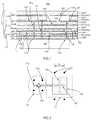
- FIG. 1a cross-sectional view of a package structure 100 is shown in accordance with one illustrative embodiment.
- the structure 100provides a mechanism to suppress or reduce parallel-plate modes and provides more feed line options using a cavity-backed aperture-coupled patch antenna 102 .
- the aperture-coupled patch antenna 102is implemented on a top section of the package 100 .
- a reflector 104is grounded with a via or vias V 2 .
- the reflector 104 and vias V 2form a cage below an aperture/slot 106 to at least partially surround the antenna area.
- Parallel-plate modesare excited by the aperture 106 .
- the parallel-plate modesare strong if the aperture also radiates, which is the case for wideband applications.
- a spacing Sv ( FIG. 2 ) between V 2 viasmay be, e.g., less than 0.25 times the wavelength of the antenna operating frequency to prevent RF leakage.
- RF connections between the antenna 102 and an RFIC chip 108are vertical coaxial-like transmission lines realized with vias V 1 and V 1 g .
- the signal line vias ( 120 )are vertically disposed surrounded by ground vias (V 1 g ) (see FIG. 2 ).
- the aperture-coupled patch antenna 102is implemented on a top section of the package 100 .
- the package 100has at least two ground planes, one ground plane 103 for the antenna in metal layer M 1 and another ground plane in metal layer M 3 for the reflector 104 .
- a power plane 105can also function as the reflector for the antenna to reduce the back radiation.
- the reflector 104may be implemented somewhere between the power plane 105 and an antenna feed line 107 .
- the antenna 102is coupled to the RFIC chip 108 through the antenna feed line 107 which undergoes a vertical transition.
- the vertical transition(signal via V 1 ) has good performance, since it behaves like a coaxial cable with an outside shield formed with grounded vias, e.g., V 1 g.
- a package interface to the chip 108 and a printed circuit board (PCB) (not shown)is implemented at a bottom section of the package 100 .
- Via V 3 gis a ground plane via, and via V 3 p is a power plane via. Via V 3 s is a signal via.
- optional metal layer Momay be employed to reduce package layout complexities.
- Metal layer M 5is a ground plane for the chip 108 .
- Metal layer M 1is a ground plane for the antenna 102 and aperture/slot 106 .
- Metal layer M 0forms the antenna 102 .
- Metal layer M 3is employed for the reflector 104 .
- Metal layer M 6is employed for pads ( 110 , 112 ).
- Metal layers M 2 , M 4 and M 6 as well as portions of other metal layersform metal lines and connections between components. It should be understood that a greater number or fewer metal layers and different configurations thereof may be employed within the scope of the present principles. For example, depending on the application, more metal and substrate layers can be added between the power plane M 4 and chip ground plane M 5 .
- the package 100may include, e.g., substrate layers Sub 0 -Sub 5 on which the metal layers are patterned and prepreg (or adhesive) layers Prepreg 0 -Prepreg 4 .
- prepreg (or adhesive) layersPrepreg 0 -Prepreg 4 .
- a different number of layersmay also be employed.
- FIG. 2a planar view of the package 100 is shown.
- the slot 106 and cavity 114are shown in phantom lines.
- the spacing Sv between vias V 2is shown.
- a signal via V 1 120couples a feed line 113 on a different layer to a feed line 107 for the antenna/patch 102 .
- the signal via 120is surrounded by ground vias (e.g., V 1 g ) to provide a vertical transition 124 .
- the package 100can be made in three stages.
- metal structures on metal layers M 4 , optional Mo, M 5 and M 6can be made and substrates Sub 4 , Prepreg 4 and Sub 5 are laminated together.
- the plated-through holes(vias V 3 g , V 3 p , V 3 s ) are fabricated afterward.
- Metal structures on metal layers M 1 , M 2 and M 3can be made, and substrates Sub 2 , Prepreg 2 and Sub 3 are laminated together.
- the plated-through holes (vias V 2 )are made afterward. This forms L 1 c .
- a lamination processmay be employed to form L 1 p.
- L 1 b , Prepreg 3 and L 1 care laminated together, and plated-through holes (vias V 1 and V 1 g ) are made afterward. This forms L 2 .
- L 2 , L 1 p (Sub 0 , Prepreg 0 , Sub 1 ), and Prepreg 1are laminated together.
- via V 1may stop at the antenna ground plane level (M 1 ), instead of at the feed line level (M 2 ), but with an antipad so that the via V 1 does not touch the ground plane.
- V 3 sstops at the power plane level (M 4 ), instead of at the metal Mo level, but with an antipad so that the via V 3 s does not touch the power plane.
- Via V 3 gmay stop at the metal layer M 5 , but may reach the M 4 level using an antipad.
- LTCClow temperature cofired ceramic
- a package structure 200implements aperture-coupled stacked patch antennas 202 , 204 .
- no cavityis employed and the patch 204 is formed on Sub 0 in a metal layer Ms.
- the patch 202is formed on metal layer M 0 .
- a package structure 201may include a regular aperture-coupled patch antenna 206 .
- Patch 206is formed on Sub 1 in metal layer M 0 with no cavity. The package production cost is lowered since no internal cavity is used.
- a slot or slot loop antenna 210may be employed, for example.
- a planar view of a vertical differential transition implementation 300is illustratively shown.
- a vertical differential transition 302can be accommodated in the present package structure.
- the differential feed methodcan be employed with, e.g., the cavity-backed patch antenna of FIG. 1 , the stacked patch antenna of FIG. 3 , the regular patch antenna of FIG. 4 , or the slot (or slot loop) antenna of FIG. 5 .
- the vertical transition 302includes a differential feed line 304 from someplace in the package, e.g., on the bottom surface of the package.
- Differential signal vias 306carry the signals to differential feed lines 308 which interact with a patch 310 and slots 312 to propagate the differential signal.
- a cavity 314 and slots 312are depicted in phantom lines.
- the vias 306are surrounded by ground vias 311 .
- FIGS. 7 and 8planar views of package structures using slot loop antennas with single-ended ( FIG. 7 ) or differential feed lines ( FIG. 8 ) are shown.
- a slot loop 412is shown in phantom lines.
- a vertical transition 402includes feed lines 404 from someplace in the package. The vertical transition is surrounded by ground vias 410 .
- Signal vias 406carry the signals to feed lines 408 which interact with slot loops 412 to propagate the signal.
- Ground vias 411surround the slot region as well.
- a 2 ⁇ 2 (4-element) phased array 500is shown in accordance with the present principles.
- the phased arraymay include any number of elements, but in this example 4 elements are illustratively depicted. All four antennas are in a same package (e.g., package 100 or other package in accordance with the present principles).
- the array 500includes a single RFIC chip 502 with four feed lines 504 to each antenna 506 .
- the antennas 506include patch antennas in this embodiment although other antennas may be employed.
- the feed lines 504connect to a signal via 508 , which is surrounded by ground vias 511 .
- the signal via 508connects to a feed line 510 for each patch antenna 506 .
- the patches 506have a corresponding reflector and vias that form a cage to reduce parallel-plate modes.
- an illustrative configuration 550includes the package 100 having an RFIC chip 108 attached along with two PCBs 530 and 532 . Pads 534 connecting RFIC chip 108 to PCB 532 through the package 100 are illustratively depicted. If heat is an issue in the configuration 550 , a heat sink 536 may be employed and attached to the RFIC chip 108 and/or the PCBs 530 and 532 .
- the PCB's 530 and 532may be separate PCBs or may be a single PCB (a motherboard or the like).
- a method for fabricating a package structure with suppressed parallel-plate mode excitation for an integrated antennais illustratively shown.
- a portione.g., a bottom
- the substratesmay include prepregnated boards (epoxy resin boards) or other substrate boards or materials.
- the boards or substratesinclude metal layers formed and patterned thereon using known methods.
- the portionprovides an interface for at least one integrated circuit chip.
- the interfaceincludes pads to connect to the at least one integrated circuit, to connect to an external printed wiring board (e.g., a motherboard), etc.
- the padsare preferably external to the package and permit the integrated circuit (e.g., RFIC) or PCBs to be connected externally to the package. This obviates the need to form cavities, recesses or other features within the package itself and thereby reduces cost.
- integrated circuite.g., RFIC
- PCBsPCBs
- a parallel-plate mode suppression mechanismis formed for the package structure using substrates with metal layers and vias.
- the parallel-plate mode suppression mechanismincludes a reflector and first grounded vias to form a cage structure.
- the parallel-plate mode suppression mechanismpreferably includes forming the reflector and the antenna ground plane on separate layers and having a different footprint for the reflector and the antenna ground plane.
- another (e.g., top) portion of the package structureis formed using substrates with metal layers formed thereon to provide an integrated antenna.
- the antennamay include a regular patch antenna, a stacked patch antenna, a cavity-backed aperture-coupled patch antenna, a slot antenna, a slot loop antenna, etc.
- the antennamay include single or differential feed lines. A plurality of antennas may be employed in a phased array.
- fabricating viasis performed.
- plated-via through holesare formed after forming each of the portions, (e.g., top and bottom) and the parallel-plate mode suppression mechanism in block 610 .
- viasare fabricated/provided as embedded vias using low temperature cofired ceramic (LTCC) technology.
- LTCClow temperature cofired ceramic
- the first grounded viasinclude a spacing dependent on an operating wavelength of the antenna, e.g., less than 0.25 times an operating wavelength of the antenna.
- the portions (e.g., top and bottom) and the parallel-plate mode suppression mechanismare laminated such that the cage structure at least partially encloses an antenna region and the reflector is preferably vertically and horizontally offset from an antenna ground plane.
- the at least one integrated circuit chipmay include a radio frequency integrated circuit (RFIC), PCB, etc. The RFIC, PCB, etc. may be bonded to bond pads of the bottom portion.
- RFICradio frequency integrated circuit
Landscapes
- Engineering & Computer Science (AREA)
- Microelectronics & Electronic Packaging (AREA)
- Computer Hardware Design (AREA)
- Physics & Mathematics (AREA)
- General Physics & Mathematics (AREA)
- Condensed Matter Physics & Semiconductors (AREA)
- Power Engineering (AREA)
- Computer Networks & Wireless Communication (AREA)
- Theoretical Computer Science (AREA)
- Variable-Direction Aerials And Aerial Arrays (AREA)
- Waveguide Aerials (AREA)
Abstract
Description
Claims (16)
Priority Applications (2)
| Application Number | Priority Date | Filing Date | Title |
|---|---|---|---|
| US13/029,657US8988299B2 (en) | 2011-02-17 | 2011-02-17 | Integrated antenna for RFIC package applications |
| US14/603,856US9172132B2 (en) | 2011-02-17 | 2015-01-23 | Integrated antenna for RFIC package applications |
Applications Claiming Priority (1)
| Application Number | Priority Date | Filing Date | Title |
|---|---|---|---|
| US13/029,657US8988299B2 (en) | 2011-02-17 | 2011-02-17 | Integrated antenna for RFIC package applications |
Related Child Applications (1)
| Application Number | Title | Priority Date | Filing Date |
|---|---|---|---|
| US14/603,856ContinuationUS9172132B2 (en) | 2011-02-17 | 2015-01-23 | Integrated antenna for RFIC package applications |
Publications (2)
| Publication Number | Publication Date |
|---|---|
| US20120212384A1 US20120212384A1 (en) | 2012-08-23 |
| US8988299B2true US8988299B2 (en) | 2015-03-24 |
Family
ID=46652295
Family Applications (2)
| Application Number | Title | Priority Date | Filing Date |
|---|---|---|---|
| US13/029,657Active2032-10-23US8988299B2 (en) | 2011-02-17 | 2011-02-17 | Integrated antenna for RFIC package applications |
| US14/603,856ActiveUS9172132B2 (en) | 2011-02-17 | 2015-01-23 | Integrated antenna for RFIC package applications |
Family Applications After (1)
| Application Number | Title | Priority Date | Filing Date |
|---|---|---|---|
| US14/603,856ActiveUS9172132B2 (en) | 2011-02-17 | 2015-01-23 | Integrated antenna for RFIC package applications |
Country Status (1)
| Country | Link |
|---|---|
| US (2) | US8988299B2 (en) |
Cited By (73)
| Publication number | Priority date | Publication date | Assignee | Title |
|---|---|---|---|---|
| US20150129668A1 (en)* | 2011-02-17 | 2015-05-14 | International Business Machines Corporation | Integrated antenna for rfic package applications |
| US20150130681A1 (en)* | 2013-11-08 | 2015-05-14 | Taiwan Semiconductor Manufacturing Company, Ltd. | 3d antenna for integrated circuits |
| US9331030B1 (en)* | 2014-12-15 | 2016-05-03 | Industrial Technology Research Institute | Integrated antenna package and manufacturing method thereof |
| US20160276731A1 (en)* | 2012-10-22 | 2016-09-22 | Texas Instruments Incorporated | Waveguide coupler |
| US9985346B2 (en) | 2014-08-13 | 2018-05-29 | International Business Machines Corporation | Wireless communications package with integrated antennas and air cavity |
| US10396437B2 (en)* | 2017-09-22 | 2019-08-27 | Lg Electronics Inc. | Mobile terminal |
| US10483618B2 (en)* | 2017-11-02 | 2019-11-19 | Samsung Electronics Co., Ltd. | Semiconductor package and manufacturing method thereof |
| WO2019236085A1 (en)* | 2018-06-07 | 2019-12-12 | Hewlett-Packard Development Company, L.P. | Front-end modules with ground plane slots |
| US10522499B2 (en) | 2017-02-09 | 2019-12-31 | Invensas Bonding Technologies, Inc. | Bonded structures |
| US10546832B2 (en) | 2016-12-21 | 2020-01-28 | Invensas Bonding Technologies, Inc. | Bonded structures |
| US10594019B2 (en) | 2016-12-03 | 2020-03-17 | International Business Machines Corporation | Wireless communications package with integrated antenna array |
| US10607937B2 (en) | 2015-12-18 | 2020-03-31 | Invensas Bonding Technologies, Inc. | Increased contact alignment tolerance for direct bonding |
| US10693207B2 (en)* | 2018-06-29 | 2020-06-23 | Ciena Corporation | Printed circuit boards and methods for manufacturing thereof for RF connectivity between electro-optic phase modulator and digital signal processor |
| US20200212536A1 (en)* | 2018-12-31 | 2020-07-02 | Texas Instruments Incorporated | Wireless communication device with antenna on package |
| US10777533B2 (en) | 2012-08-30 | 2020-09-15 | Invensas Bonding Technologies, Inc. | Heterogeneous device |
| US10784191B2 (en) | 2017-03-31 | 2020-09-22 | Invensas Bonding Technologies, Inc. | Interface structures and methods for forming same |
| US10840205B2 (en) | 2017-09-24 | 2020-11-17 | Invensas Bonding Technologies, Inc. | Chemical mechanical polishing for hybrid bonding |
| US10879226B2 (en) | 2016-05-19 | 2020-12-29 | Invensas Bonding Technologies, Inc. | Stacked dies and methods for forming bonded structures |
| US10896902B2 (en) | 2016-01-13 | 2021-01-19 | Invensas Bonding Technologies, Inc. | Systems and methods for efficient transfer of semiconductor elements |
| US10923408B2 (en) | 2017-12-22 | 2021-02-16 | Invensas Bonding Technologies, Inc. | Cavity packages |
| US10998265B2 (en) | 2016-09-30 | 2021-05-04 | Invensas Bonding Technologies, Inc. | Interface structures and methods for forming same |
| US11004757B2 (en) | 2018-05-14 | 2021-05-11 | Invensas Bonding Technologies, Inc. | Bonded structures |
| US11011418B2 (en) | 2005-08-11 | 2021-05-18 | Invensas Bonding Technologies, Inc. | 3D IC method and device |
| US11011494B2 (en) | 2018-08-31 | 2021-05-18 | Invensas Bonding Technologies, Inc. | Layer structures for making direct metal-to-metal bonds at low temperatures in microelectronics |
| US11056390B2 (en) | 2015-06-24 | 2021-07-06 | Invensas Corporation | Structures and methods for reliable packages |
| US11158573B2 (en) | 2018-10-22 | 2021-10-26 | Invensas Bonding Technologies, Inc. | Interconnect structures |
| US11169326B2 (en) | 2018-02-26 | 2021-11-09 | Invensas Bonding Technologies, Inc. | Integrated optical waveguides, direct-bonded waveguide interface joints, optical routing and interconnects |
| US11189905B2 (en) | 2018-04-13 | 2021-11-30 | International Business Machines Corporation | Integrated antenna array packaging structures and methods |
| US11205600B2 (en) | 2014-03-12 | 2021-12-21 | Invensas Corporation | Integrated circuits protected by substrates with cavities, and methods of manufacture |
| US11244920B2 (en) | 2018-12-18 | 2022-02-08 | Invensas Bonding Technologies, Inc. | Method and structures for low temperature device bonding |
| US11257727B2 (en) | 2017-03-21 | 2022-02-22 | Invensas Bonding Technologies, Inc. | Seal for microelectronic assembly |
| US11264345B2 (en) | 2015-08-25 | 2022-03-01 | Invensas Bonding Technologies, Inc. | Conductive barrier direct hybrid bonding |
| US11380597B2 (en) | 2017-12-22 | 2022-07-05 | Invensas Bonding Technologies, Inc. | Bonded structures |
| US11387214B2 (en) | 2017-06-15 | 2022-07-12 | Invensas Llc | Multi-chip modules formed using wafer-level processing of a reconstituted wafer |
| US11393779B2 (en) | 2018-06-13 | 2022-07-19 | Invensas Bonding Technologies, Inc. | Large metal pads over TSV |
| US11430750B2 (en) | 2019-05-29 | 2022-08-30 | Advanced Semiconductor Engineering, Inc. | Semiconductor device package having an antenna formed over a foaming agent filled cavity in a support layer |
| US11462419B2 (en) | 2018-07-06 | 2022-10-04 | Invensas Bonding Technologies, Inc. | Microelectronic assemblies |
| US11476213B2 (en) | 2019-01-14 | 2022-10-18 | Invensas Bonding Technologies, Inc. | Bonded structures without intervening adhesive |
| US11515291B2 (en) | 2018-08-28 | 2022-11-29 | Adeia Semiconductor Inc. | Integrated voltage regulator and passive components |
| US11515279B2 (en) | 2018-04-11 | 2022-11-29 | Adeia Semiconductor Bonding Technologies Inc. | Low temperature bonded structures |
| US11538781B2 (en) | 2020-06-30 | 2022-12-27 | Adeia Semiconductor Bonding Technologies Inc. | Integrated device packages including bonded structures |
| US11626363B2 (en) | 2016-12-29 | 2023-04-11 | Adeia Semiconductor Bonding Technologies Inc. | Bonded structures with integrated passive component |
| US11652083B2 (en) | 2017-05-11 | 2023-05-16 | Adeia Semiconductor Bonding Technologies Inc. | Processed stacked dies |
| US11664357B2 (en) | 2018-07-03 | 2023-05-30 | Adeia Semiconductor Bonding Technologies Inc. | Techniques for joining dissimilar materials in microelectronics |
| US11710718B2 (en) | 2015-07-10 | 2023-07-25 | Adeia Semiconductor Technologies Llc | Structures and methods for low temperature bonding using nanoparticles |
| US11715730B2 (en) | 2017-03-16 | 2023-08-01 | Adeia Semiconductor Technologies Llc | Direct-bonded LED arrays including optical elements configured to transmit optical signals from LED elements |
| US11728313B2 (en) | 2018-06-13 | 2023-08-15 | Adeia Semiconductor Bonding Technologies Inc. | Offset pads over TSV |
| US11728273B2 (en) | 2020-09-04 | 2023-08-15 | Adeia Semiconductor Bonding Technologies Inc. | Bonded structure with interconnect structure |
| US11735523B2 (en) | 2020-05-19 | 2023-08-22 | Adeia Semiconductor Bonding Technologies Inc. | Laterally unconfined structure |
| US11760059B2 (en) | 2003-05-19 | 2023-09-19 | Adeia Semiconductor Bonding Technologies Inc. | Method of room temperature covalent bonding |
| US11764477B2 (en) | 2021-12-24 | 2023-09-19 | Richwave Technology Corp. | Antenna apparatus |
| US11764189B2 (en) | 2018-07-06 | 2023-09-19 | Adeia Semiconductor Bonding Technologies Inc. | Molded direct bonded and interconnected stack |
| US11762200B2 (en) | 2019-12-17 | 2023-09-19 | Adeia Semiconductor Bonding Technologies Inc. | Bonded optical devices |
| US11764177B2 (en) | 2020-09-04 | 2023-09-19 | Adeia Semiconductor Bonding Technologies Inc. | Bonded structure with interconnect structure |
| US11804377B2 (en) | 2018-04-05 | 2023-10-31 | Adeia Semiconductor Bonding Technologies, Inc. | Method for preparing a surface for direct-bonding |
| US11881454B2 (en) | 2016-10-07 | 2024-01-23 | Adeia Semiconductor Inc. | Stacked IC structure with orthogonal interconnect layers |
| US11894326B2 (en) | 2017-03-17 | 2024-02-06 | Adeia Semiconductor Bonding Technologies Inc. | Multi-metal contact structure |
| US11901281B2 (en) | 2019-03-11 | 2024-02-13 | Adeia Semiconductor Bonding Technologies Inc. | Bonded structures with integrated passive component |
| US11908739B2 (en) | 2017-06-05 | 2024-02-20 | Adeia Semiconductor Technologies Llc | Flat metal features for microelectronics applications |
| US11916054B2 (en) | 2018-05-15 | 2024-02-27 | Adeia Semiconductor Bonding Technologies Inc. | Stacked devices and methods of fabrication |
| US11929347B2 (en) | 2020-10-20 | 2024-03-12 | Adeia Semiconductor Technologies Llc | Mixed exposure for large die |
| US11935907B2 (en) | 2014-12-11 | 2024-03-19 | Adeia Semiconductor Technologies Llc | Image sensor device |
| US11955463B2 (en) | 2019-06-26 | 2024-04-09 | Adeia Semiconductor Bonding Technologies Inc. | Direct bonded stack structures for increased reliability and improved yield in microelectronics |
| US11973056B2 (en) | 2016-10-27 | 2024-04-30 | Adeia Semiconductor Technologies Llc | Methods for low temperature bonding using nanoparticles |
| US12009338B2 (en) | 2020-03-19 | 2024-06-11 | Adeia Semiconductor Bonding Technologies Inc. | Dimension compensation control for directly bonded structures |
| US12080672B2 (en) | 2019-09-26 | 2024-09-03 | Adeia Semiconductor Bonding Technologies Inc. | Direct gang bonding methods including directly bonding first element to second element to form bonded structure without adhesive |
| US12100676B2 (en) | 2018-04-11 | 2024-09-24 | Adeia Semiconductor Bonding Technologies Inc. | Low temperature bonded structures |
| US12211809B2 (en) | 2020-12-30 | 2025-01-28 | Adeia Semiconductor Bonding Technologies Inc. | Structure with conductive feature and method of forming same |
| US12270970B2 (en) | 2018-03-20 | 2025-04-08 | Adeia Semiconductor Bonding Technologies Inc. | Direct-bonded lamination for improved image clarity in optical devices |
| US12347912B2 (en) | 2022-06-28 | 2025-07-01 | Unimicron Technology Corp | Multi-layered resonator circuit structure and multi-layered filter circuit structure |
| US12374641B2 (en) | 2019-06-12 | 2025-07-29 | Adeia Semiconductor Bonding Technologies Inc. | Sealed bonded structures and methods for forming the same |
| US12381128B2 (en) | 2020-12-28 | 2025-08-05 | Adeia Semiconductor Bonding Technologies Inc. | Structures with through-substrate vias and methods for forming the same |
| US12424584B2 (en) | 2020-10-29 | 2025-09-23 | Adeia Semiconductor Bonding Technologies Inc. | Direct bonding methods and structures |
Families Citing this family (136)
| Publication number | Priority date | Publication date | Assignee | Title |
|---|---|---|---|---|
| US9742077B2 (en)* | 2011-03-15 | 2017-08-22 | Intel Corporation | Mm-wave phased array antenna with beam tilting radiation pattern |
| US9153863B2 (en) | 2012-01-24 | 2015-10-06 | E I Du Pont De Nemours And Company | Low temperature co-fired ceramic (LTCC) system in a package (SiP) configurations for microwave/millimeter wave packaging applications |
| FR2992103B1 (en)* | 2012-06-19 | 2014-06-13 | St Microelectronics Sa | INTEGRATED THREE-DIMENSIONAL STRUCTURE COMPRISING AN ANTENNA |
| US9721920B2 (en)* | 2012-10-19 | 2017-08-01 | Infineon Technologies Ag | Embedded chip packages and methods for manufacturing an embedded chip package |
| US9252491B2 (en) | 2012-11-30 | 2016-02-02 | Taiwan Semiconductor Manufacturing Company, Ltd. | Embedding low-k materials in antennas |
| CN203279336U (en)* | 2013-04-27 | 2013-11-06 | 中兴通讯股份有限公司 | Inner heat dissipation terminal |
| CN103441332B (en)* | 2013-08-21 | 2016-12-28 | 华为技术有限公司 | A kind of micro-strip array antenna and base station |
| US9819098B2 (en) | 2013-09-11 | 2017-11-14 | International Business Machines Corporation | Antenna-in-package structures with broadside and end-fire radiations |
| US9806422B2 (en) | 2013-09-11 | 2017-10-31 | International Business Machines Corporation | Antenna-in-package structures with broadside and end-fire radiations |
| JP2015065553A (en)* | 2013-09-25 | 2015-04-09 | 株式会社東芝 | Connection member, semiconductor device, and laminate structure |
| TWI557983B (en) | 2014-04-16 | 2016-11-11 | Nat Inst Chung Shan Science & Technology | Non - planar Antenna Embedded Packaging Structure and Its Making Method |
| JP6196188B2 (en)* | 2014-06-17 | 2017-09-13 | 株式会社東芝 | ANTENNA DEVICE AND RADIO DEVICE |
| WO2016067969A1 (en)* | 2014-10-31 | 2016-05-06 | 株式会社村田製作所 | Antenna module and circuit module |
| US9972902B2 (en)* | 2014-11-04 | 2018-05-15 | Panasonic Intellectual Property Management Co., Ltd. | Antenna device and electronic device |
| US9871299B2 (en)* | 2014-12-04 | 2018-01-16 | Qualcomm Incorporated | Cavity backed aperture antenna |
| DE102015201445A1 (en)* | 2015-01-28 | 2016-07-28 | Robert Bosch Gmbh | radar sensor |
| WO2016134739A1 (en) | 2015-02-23 | 2016-09-01 | Huawei Technologies Co., Ltd. | Radio frequency circuit and communication device module |
| US10361476B2 (en)* | 2015-05-26 | 2019-07-23 | Qualcomm Incorporated | Antenna structures for wireless communications |
| DE102015113322B3 (en)* | 2015-08-12 | 2016-11-17 | Schweizer Electronic Ag | Radio-frequency antenna, radio-frequency substrate with radio-frequency antenna and method of production |
| US9865926B2 (en) | 2015-09-02 | 2018-01-09 | Qualcomm Incorporated | Low angle radiating shorted half patch antenna |
| US10083923B2 (en)* | 2015-09-21 | 2018-09-25 | Intel Corporation | Platform with thermally stable wireless interconnects |
| EP3211976A1 (en)* | 2016-02-29 | 2017-08-30 | AT & S Austria Technologie & Systemtechnik Aktiengesellschaft | Printed circuit board with antenna structure and method for its production |
| CN107369673B (en)* | 2016-05-13 | 2019-11-05 | 华为技术有限公司 | It is provided with the integrated circuit package device and its manufacturing method of antenna |
| CN109478723A (en)* | 2016-06-30 | 2019-03-15 | 日立金属株式会社 | Flat plane antenna, co-fired ceramic substrate and pseudo millimeteric wave/millimeter wave wireless communication components |
| US10181653B2 (en) | 2016-07-21 | 2019-01-15 | Infineon Technologies Ag | Radio frequency system for wearable device |
| US9923712B2 (en) | 2016-08-01 | 2018-03-20 | Movandi Corporation | Wireless receiver with axial ratio and cross-polarization calibration |
| US10218407B2 (en) | 2016-08-08 | 2019-02-26 | Infineon Technologies Ag | Radio frequency system and method for wearable device |
| US10014567B2 (en)* | 2016-09-02 | 2018-07-03 | Movandi Corporation | Antenna arrangements and routing configurations in large scale integration of antennas with front end chips in a wireless receiver |
| US10291296B2 (en) | 2016-09-02 | 2019-05-14 | Movandi Corporation | Transceiver for multi-beam and relay with 5G application |
| US11239186B2 (en)* | 2016-09-23 | 2022-02-01 | Intel Corporation | Die with embedded communication cavity |
| US10199717B2 (en) | 2016-11-18 | 2019-02-05 | Movandi Corporation | Phased array antenna panel having reduced passive loss of received signals |
| US10466772B2 (en) | 2017-01-09 | 2019-11-05 | Infineon Technologies Ag | System and method of gesture detection for a remote device |
| US10396432B2 (en)* | 2017-01-23 | 2019-08-27 | Samsung Electro-Mechanics Co., Ltd. | Antenna-integrated radio frequency module |
| US10505255B2 (en)* | 2017-01-30 | 2019-12-10 | Infineon Technologies Ag | Radio frequency device packages and methods of formation thereof |
| WO2018173750A1 (en)* | 2017-03-21 | 2018-09-27 | 株式会社村田製作所 | Antenna module and communication device |
| CN210074170U (en)* | 2017-04-03 | 2020-02-14 | 株式会社村田制作所 | High frequency module |
| US11069978B2 (en) | 2017-04-07 | 2021-07-20 | Skyworks Solutions, Inc. | Method of manufacturing a radio-frequency module with a conformal shield antenna |
| US20180294569A1 (en)* | 2017-04-07 | 2018-10-11 | Skyworks Solutions, Inc. | Radio-frequency module with integrated shield layer antenna and integrated cavity-based antenna |
| JP6828576B2 (en)* | 2017-04-26 | 2021-02-10 | 富士通株式会社 | High-frequency modules, wireless devices, and methods for manufacturing high-frequency modules |
| US10297927B2 (en)* | 2017-05-01 | 2019-05-21 | Intel Corporation | Antenna package for large-scale millimeter wave phased arrays |
| US10056922B1 (en) | 2017-06-14 | 2018-08-21 | Infineon Technologies Ag | Radio frequency device modules and methods of formation thereof |
| US10602548B2 (en) | 2017-06-22 | 2020-03-24 | Infineon Technologies Ag | System and method for gesture sensing |
| US10484078B2 (en) | 2017-07-11 | 2019-11-19 | Movandi Corporation | Reconfigurable and modular active repeater device |
| US11394103B2 (en)* | 2017-07-18 | 2022-07-19 | Samsung Electro-Mechanics Co., Ltd. | Antenna module and manufacturing method thereof |
| KR102362243B1 (en)* | 2017-10-18 | 2022-02-11 | 삼성전자주식회사 | Radio frequency package module and electronic apparatus including the same |
| CN107910311B (en)* | 2017-12-04 | 2024-06-14 | 盛合晶微半导体(江阴)有限公司 | Fan-out type antenna packaging structure and preparation method thereof |
| CN110034394B (en) | 2018-01-11 | 2023-06-20 | 三星电子株式会社 | Multi-feed patch antenna and device comprising multi-feed patch antenna |
| US11278241B2 (en) | 2018-01-16 | 2022-03-22 | Infineon Technologies Ag | System and method for vital signal sensing using a millimeter-wave radar sensor |
| US11346936B2 (en) | 2018-01-16 | 2022-05-31 | Infineon Technologies Ag | System and method for vital signal sensing using a millimeter-wave radar sensor |
| US10795012B2 (en) | 2018-01-22 | 2020-10-06 | Infineon Technologies Ag | System and method for human behavior modelling and power control using a millimeter-wave radar sensor |
| US10576328B2 (en) | 2018-02-06 | 2020-03-03 | Infineon Technologies Ag | System and method for contactless sensing on a treadmill |
| DE102018202364B4 (en)* | 2018-02-15 | 2022-10-13 | Fraunhofer-Gesellschaft zur Förderung der angewandten Forschung e.V. | Module unit with integrated antennas and method for manufacturing the same |
| US10705198B2 (en) | 2018-03-27 | 2020-07-07 | Infineon Technologies Ag | System and method of monitoring an air flow using a millimeter-wave radar sensor |
| US11336015B2 (en) | 2018-03-28 | 2022-05-17 | Intel Corporation | Antenna boards and communication devices |
| US11380979B2 (en) | 2018-03-29 | 2022-07-05 | Intel Corporation | Antenna modules and communication devices |
| JP6564902B1 (en) | 2018-03-30 | 2019-08-21 | 株式会社フジクラ | antenna |
| JP6712613B2 (en)* | 2018-03-30 | 2020-06-24 | 株式会社フジクラ | antenna |
| US11652301B2 (en) | 2018-04-11 | 2023-05-16 | Qualcomm Incorporated | Patch antenna array |
| US10775482B2 (en) | 2018-04-11 | 2020-09-15 | Infineon Technologies Ag | Human detection and identification in a setting using millimeter-wave radar |
| US10761187B2 (en) | 2018-04-11 | 2020-09-01 | Infineon Technologies Ag | Liquid detection using millimeter-wave radar sensor |
| CN110401008B (en)* | 2018-04-25 | 2022-02-25 | 华为技术有限公司 | Package architecture and communication device with packaged antenna |
| US10794841B2 (en) | 2018-05-07 | 2020-10-06 | Infineon Technologies Ag | Composite material structure monitoring system |
| US11011827B2 (en)* | 2018-05-11 | 2021-05-18 | Intel IP Corporation | Antenna boards and communication devices |
| US10399393B1 (en) | 2018-05-29 | 2019-09-03 | Infineon Technologies Ag | Radar sensor system for tire monitoring |
| US11509037B2 (en)* | 2018-05-29 | 2022-11-22 | Intel Corporation | Integrated circuit packages, antenna modules, and communication devices |
| US10903567B2 (en) | 2018-06-04 | 2021-01-26 | Infineon Technologies Ag | Calibrating a phased array system |
| US10797394B2 (en) | 2018-06-05 | 2020-10-06 | Intel Corporation | Antenna modules and communication devices |
| CN111919335A (en)* | 2018-07-17 | 2020-11-10 | 华为技术有限公司 | An integrated circuit and terminal equipment |
| US11416077B2 (en) | 2018-07-19 | 2022-08-16 | Infineon Technologies Ag | Gesture detection system and method using a radar sensor |
| AU2019315962B2 (en) | 2018-08-02 | 2025-03-27 | Viasat, Inc. | Antenna element module |
| CN110828962B (en) | 2018-08-09 | 2021-08-03 | 财团法人工业技术研究院 | Antenna array module and manufacturing method thereof |
| US10928501B2 (en) | 2018-08-28 | 2021-02-23 | Infineon Technologies Ag | Target detection in rainfall and snowfall conditions using mmWave radar |
| US11183772B2 (en) | 2018-09-13 | 2021-11-23 | Infineon Technologies Ag | Embedded downlight and radar system |
| US10373901B1 (en) | 2018-09-26 | 2019-08-06 | Taiwan Semiconductor Manufacturing Company Ltd. | Semiconductor structure and manufacturing method thereof |
| US11125869B2 (en) | 2018-10-16 | 2021-09-21 | Infineon Technologies Ag | Estimating angle of human target using mmWave radar |
| US10971798B2 (en) | 2018-10-18 | 2021-04-06 | Advanced Semiconductor Engineering, Inc. | Semiconductor device package and method of manufacturing the same |
| US11397239B2 (en) | 2018-10-24 | 2022-07-26 | Infineon Technologies Ag | Radar sensor FSM low power mode |
| US11360185B2 (en) | 2018-10-24 | 2022-06-14 | Infineon Technologies Ag | Phase coded FMCW radar |
| EP3654053A1 (en) | 2018-11-14 | 2020-05-20 | Infineon Technologies AG | Package with acoustic sensing device(s) and millimeter wave sensing elements |
| CN109449589B (en)* | 2018-12-17 | 2023-12-29 | 西安电子工程研究所 | Two-dimensional active phased array antenna unit with wide bandwidth sweep characteristics |
| CN109727934B (en)* | 2018-12-28 | 2024-05-31 | 盛合晶微半导体(江阴)有限公司 | Packaging structure and preparation method thereof |
| CN109586004A (en)* | 2018-12-29 | 2019-04-05 | 瑞声科技(南京)有限公司 | A kind of encapsulating antenna mould group and electronic equipment |
| CN110190376B (en)* | 2018-12-31 | 2020-12-04 | 杭州臻镭微波技术有限公司 | Radio frequency system-in-package module with antenna combined with liquid cooling heat dissipation structure and manufacturing method thereof |
| US11087115B2 (en) | 2019-01-22 | 2021-08-10 | Infineon Technologies Ag | User authentication using mm-Wave sensor for automotive radar systems |
| US12015191B2 (en) | 2019-02-08 | 2024-06-18 | Texas Instruments Incorporated | Antenna-on-package integrated circuit device |
| CN109742056A (en)* | 2019-02-18 | 2019-05-10 | 中芯长电半导体(江阴)有限公司 | Antenna packaging structure and packaging method |
| CN109768032B (en)* | 2019-03-04 | 2023-10-31 | 盛合晶微半导体(江阴)有限公司 | Antenna packaging structure and packaging method |
| WO2020177849A1 (en)* | 2019-03-04 | 2020-09-10 | Huawei Technologies Co., Ltd. | A unibody for an electronic device |
| US11355838B2 (en) | 2019-03-18 | 2022-06-07 | Infineon Technologies Ag | Integration of EBG structures (single layer/multi-layer) for isolation enhancement in multilayer embedded packaging technology at mmWave |
| US11126885B2 (en) | 2019-03-21 | 2021-09-21 | Infineon Technologies Ag | Character recognition in air-writing based on network of radars |
| US12021315B2 (en) | 2019-03-22 | 2024-06-25 | Commscope Technologies Llc | Dual-polarized radiating elements for base station antennas having built-in common-mode rejection filters that block common mode radiation parasitics |
| WO2020197849A1 (en)* | 2019-03-22 | 2020-10-01 | Commscope Technologies Llc | Dual-polarized radiating elements for base station antennas having built-in stalk filters that block common mode radiation parasitics |
| CN111755812A (en)* | 2019-03-28 | 2020-10-09 | 电连技术股份有限公司 | Antenna modules and terminals |
| US11454696B2 (en) | 2019-04-05 | 2022-09-27 | Infineon Technologies Ag | FMCW radar integration with communication system |
| WO2020231239A1 (en) | 2019-05-16 | 2020-11-19 | Samsung Electronics Co., Ltd. | Printed circuit board including coaxial plated through hole and electronic apparatus including same in wireless communication system |
| CN110085973B (en)* | 2019-05-23 | 2024-12-03 | 盛合晶微半导体(江阴)有限公司 | Antenna packaging structure and packaging method |
| CN110060983B (en)* | 2019-05-23 | 2024-06-25 | 盛合晶微半导体(江阴)有限公司 | Antenna packaging structure and packaging method |
| CN110148587B (en)* | 2019-06-06 | 2023-09-08 | 盛合晶微半导体(江阴)有限公司 | Fan-out type antenna packaging structure and packaging method |
| KR102593888B1 (en)* | 2019-06-13 | 2023-10-24 | 삼성전기주식회사 | Antenna module and electronic device including thereof |
| US11327167B2 (en) | 2019-09-13 | 2022-05-10 | Infineon Technologies Ag | Human target tracking system and method |
| US11774592B2 (en) | 2019-09-18 | 2023-10-03 | Infineon Technologies Ag | Multimode communication and radar system resource allocation |
| US11862857B2 (en) | 2019-09-30 | 2024-01-02 | Qualcomm Incorporated | Multi-band antenna system |
| US11435443B2 (en) | 2019-10-22 | 2022-09-06 | Infineon Technologies Ag | Integration of tracking with classifier in mmwave radar |
| CN112713140B (en)* | 2019-10-25 | 2025-06-13 | 盛合晶微半导体(江阴)有限公司 | Antenna packaging structure and packaging method |
| CN112713096B (en)* | 2019-10-25 | 2025-01-24 | 盛合晶微半导体(江阴)有限公司 | Antenna packaging structure and packaging method |
| US11468146B2 (en) | 2019-12-06 | 2022-10-11 | Globalfoundries U.S. Inc. | Array of integrated pixel and memory cells for deep in-sensor, in-memory computing |
| KR102731798B1 (en)* | 2019-12-10 | 2024-11-19 | 삼성전기주식회사 | Antenna substrate and antenna module comprising the same |
| US11276654B2 (en)* | 2019-12-17 | 2022-03-15 | Nxp Usa, Inc. | Bottom-side heatsinking waveguide for an integrated circuit package |
| DE102020102037A1 (en)* | 2020-01-28 | 2021-07-29 | Krohne Messtechnik Gmbh | Radar array |
| US11808883B2 (en) | 2020-01-31 | 2023-11-07 | Infineon Technologies Ag | Synchronization of multiple mmWave devices |
| US11614516B2 (en) | 2020-02-19 | 2023-03-28 | Infineon Technologies Ag | Radar vital signal tracking using a Kalman filter |
| US11195580B2 (en) | 2020-02-26 | 2021-12-07 | Globalfoundries U.S. Inc. | Integrated pixel and two-terminal non-volatile memory cell and an array of cells for deep in-sensor, in-memory computing |
| US11075453B1 (en) | 2020-02-28 | 2021-07-27 | Globalfoundries U.S. Inc. | Microelectronics package with ultra-low-K dielectric region between stacked antenna elements |
| US11069402B1 (en) | 2020-03-17 | 2021-07-20 | Globalfoundries U.S. Inc. | Integrated pixel and three-terminal non-volatile memory cell and an array of cells for deep in-sensor, in-memory computing |
| US11585891B2 (en) | 2020-04-20 | 2023-02-21 | Infineon Technologies Ag | Radar-based vital sign estimation |
| US11567185B2 (en) | 2020-05-05 | 2023-01-31 | Infineon Technologies Ag | Radar-based target tracking using motion detection |
| CN111541006A (en)* | 2020-05-21 | 2020-08-14 | 中国电子科技集团公司第十四研究所 | Glass-based patch antenna unit |
| US11774553B2 (en) | 2020-06-18 | 2023-10-03 | Infineon Technologies Ag | Parametric CNN for radar processing |
| US11704917B2 (en) | 2020-07-09 | 2023-07-18 | Infineon Technologies Ag | Multi-sensor analysis of food |
| US11614511B2 (en) | 2020-09-17 | 2023-03-28 | Infineon Technologies Ag | Radar interference mitigation |
| US11719787B2 (en) | 2020-10-30 | 2023-08-08 | Infineon Technologies Ag | Radar-based target set generation |
| US11719805B2 (en) | 2020-11-18 | 2023-08-08 | Infineon Technologies Ag | Radar based tracker using empirical mode decomposition (EMD) and invariant feature transform (IFT) |
| JP7304542B2 (en)* | 2020-12-28 | 2023-07-07 | パナソニックIpマネジメント株式会社 | antenna device |
| CN113013154B (en)* | 2021-02-10 | 2023-08-18 | 西南电子技术研究所(中国电子科技集团公司第十研究所) | Integrated packaging tube shell of flat phased array antenna transceiver component |
| US12189021B2 (en) | 2021-02-18 | 2025-01-07 | Infineon Technologies Ag | Radar-based target tracker |
| US11662430B2 (en) | 2021-03-17 | 2023-05-30 | Infineon Technologies Ag | MmWave radar testing |
| US12062863B2 (en)* | 2021-03-26 | 2024-08-13 | Sony Group Corporation | Antenna device |
| US11950895B2 (en) | 2021-05-28 | 2024-04-09 | Infineon Technologies Ag | Radar sensor system for blood pressure sensing, and associated method |
| US12307761B2 (en) | 2021-08-06 | 2025-05-20 | Infineon Technologies Ag | Scene-adaptive radar |
| US12405351B2 (en) | 2022-03-25 | 2025-09-02 | Infineon Technologies Ag | Adaptive Tx-Rx crosstalk cancellation for radar systems |
| US12399254B2 (en) | 2022-06-07 | 2025-08-26 | Infineon Technologies Ag | Radar-based single target vital sensing |
| US12399271B2 (en) | 2022-07-20 | 2025-08-26 | Infineon Technologies Ag | Radar-based target tracker |
| US12254670B2 (en) | 2022-07-29 | 2025-03-18 | Infineon Technologies Ag | Radar-based activity classification |
| CN119678660A (en)* | 2022-08-09 | 2025-03-21 | 昕诺飞控股有限公司 | Hybrid PCB with planar antenna |
| CN119726122A (en)* | 2023-09-28 | 2025-03-28 | 中国科学院微电子研究所 | Multi-band and multi-functional antenna integrated module and preparation method thereof |
| CN117497532B (en)* | 2024-01-02 | 2024-04-09 | 成都雷电微力科技股份有限公司 | AIP three-dimensional stacking TR airtight packaging assembly |
Citations (11)
| Publication number | Priority date | Publication date | Assignee | Title |
|---|---|---|---|---|
| US5023624A (en) | 1988-10-26 | 1991-06-11 | Harris Corporation | Microwave chip carrier package having cover-mounted antenna element |
| JP2001028413A (en)* | 1996-02-29 | 2001-01-30 | Kyocera Corp | High frequency package |
| US20030103006A1 (en)* | 2000-06-30 | 2003-06-05 | Atsushi Yamada | Radio communication device with integrated antenna, transmitter, and receiver |
| WO2003047033A1 (en) | 2001-11-21 | 2003-06-05 | Lockheed Martin Corporation | Scaleable antenna array architecture using standard radiating subarrays and amplifying/beamforming assemblies |
| US6989791B2 (en) | 2002-07-19 | 2006-01-24 | The Boeing Company | Antenna-integrated printed wiring board assembly for a phased array antenna system |
| US20070120742A1 (en)* | 2002-11-07 | 2007-05-31 | Fractus, S.A. | Radio-frequency system in package including antenna |
| US20080291115A1 (en)* | 2007-05-22 | 2008-11-27 | Sibeam, Inc. | Surface mountable integrated circuit packaging scheme |
| US20090273517A1 (en) | 2008-05-01 | 2009-11-05 | Emag Technologies, Inc. | Vertically integrated electronically steered phased array and method for packaging |
| US20100001906A1 (en)* | 2008-07-07 | 2010-01-07 | Akkermans Johannes A G | Radio frequency (rf) integrated circuit (ic) packages having characteristics suitable for mass production |
| US7671696B1 (en) | 2006-09-21 | 2010-03-02 | Raytheon Company | Radio frequency interconnect circuits and techniques |
| US7696930B2 (en) | 2008-04-14 | 2010-04-13 | International Business Machines Corporation | Radio frequency (RF) integrated circuit (IC) packages with integrated aperture-coupled patch antenna(s) in ring and/or offset cavities |
Family Cites Families (1)
| Publication number | Priority date | Publication date | Assignee | Title |
|---|---|---|---|---|
| US8988299B2 (en)* | 2011-02-17 | 2015-03-24 | International Business Machines Corporation | Integrated antenna for RFIC package applications |
- 2011
- 2011-02-17USUS13/029,657patent/US8988299B2/enactiveActive
- 2015
- 2015-01-23USUS14/603,856patent/US9172132B2/enactiveActive
Patent Citations (14)
| Publication number | Priority date | Publication date | Assignee | Title |
|---|---|---|---|---|
| US5023624A (en) | 1988-10-26 | 1991-06-11 | Harris Corporation | Microwave chip carrier package having cover-mounted antenna element |
| JP2001028413A (en)* | 1996-02-29 | 2001-01-30 | Kyocera Corp | High frequency package |
| US20030103006A1 (en)* | 2000-06-30 | 2003-06-05 | Atsushi Yamada | Radio communication device with integrated antenna, transmitter, and receiver |
| WO2003047033A1 (en) | 2001-11-21 | 2003-06-05 | Lockheed Martin Corporation | Scaleable antenna array architecture using standard radiating subarrays and amplifying/beamforming assemblies |
| US6989791B2 (en) | 2002-07-19 | 2006-01-24 | The Boeing Company | Antenna-integrated printed wiring board assembly for a phased array antenna system |
| US20070120742A1 (en)* | 2002-11-07 | 2007-05-31 | Fractus, S.A. | Radio-frequency system in package including antenna |
| US7791539B2 (en) | 2002-11-07 | 2010-09-07 | Fractus, S.A. | Radio-frequency system in package including antenna |
| US7671696B1 (en) | 2006-09-21 | 2010-03-02 | Raytheon Company | Radio frequency interconnect circuits and techniques |
| US7675465B2 (en) | 2007-05-22 | 2010-03-09 | Sibeam, Inc. | Surface mountable integrated circuit packaging scheme |
| US20080291115A1 (en)* | 2007-05-22 | 2008-11-27 | Sibeam, Inc. | Surface mountable integrated circuit packaging scheme |
| US7696930B2 (en) | 2008-04-14 | 2010-04-13 | International Business Machines Corporation | Radio frequency (RF) integrated circuit (IC) packages with integrated aperture-coupled patch antenna(s) in ring and/or offset cavities |
| US20090273517A1 (en) | 2008-05-01 | 2009-11-05 | Emag Technologies, Inc. | Vertically integrated electronically steered phased array and method for packaging |
| US20100001906A1 (en)* | 2008-07-07 | 2010-01-07 | Akkermans Johannes A G | Radio frequency (rf) integrated circuit (ic) packages having characteristics suitable for mass production |
| US7728774B2 (en) | 2008-07-07 | 2010-06-01 | International Business Machines Corporation | Radio frequency (RF) integrated circuit (IC) packages having characteristics suitable for mass production |
Non-Patent Citations (4)
| Title |
|---|
| Bhattacharyya et al "Analysis of Stripline-Fed Slot-Coupled Patch Antennas with Vias for Parallel-Plate Mode Suppression" IEEE Trans. on Antennas and Propag. vol. 46, No. 4, Apr. 1998.* |
| Bhattacharyya et al. ("Analysis of Stripline-Fed Slot-Coupled Patch Antennas with Vias for Parallel-Plate Mode Suppression", IEEE Transact. In Antennas and Propag., vol. 46, No. 4, Apr. 1998, pp. 538-548).* |
| Shengcai, J., et al. "Monopole Crescent Elliptical Antennas With Band-Notched Characteristics for UWB Applications" Tsinghua Science and Technology, vol. 14, No. 4. Aug. 2009. pp. 460-464. |
| Song, C.T.P., et al. "Novel Antenna for Packaged Integrated RF Front Ends" Proceedings of 2000 International Symposium on Antennas and Propagation (ISAP 2000). Aug. 2000. (4 Pages). |
Cited By (146)
| Publication number | Priority date | Publication date | Assignee | Title |
|---|---|---|---|---|
| US11760059B2 (en) | 2003-05-19 | 2023-09-19 | Adeia Semiconductor Bonding Technologies Inc. | Method of room temperature covalent bonding |
| US11011418B2 (en) | 2005-08-11 | 2021-05-18 | Invensas Bonding Technologies, Inc. | 3D IC method and device |
| US11289372B2 (en) | 2005-08-11 | 2022-03-29 | Invensas Bonding Technologies, Inc. | 3D IC method and device |
| US11515202B2 (en) | 2005-08-11 | 2022-11-29 | Adeia Semiconductor Bonding Technologies Inc. | 3D IC method and device |
| US20150129668A1 (en)* | 2011-02-17 | 2015-05-14 | International Business Machines Corporation | Integrated antenna for rfic package applications |
| US9172132B2 (en)* | 2011-02-17 | 2015-10-27 | Globalfoundries Inc | Integrated antenna for RFIC package applications |
| US10777533B2 (en) | 2012-08-30 | 2020-09-15 | Invensas Bonding Technologies, Inc. | Heterogeneous device |
| US11631586B2 (en) | 2012-08-30 | 2023-04-18 | Adeia Semiconductor Bonding Technologies Inc. | Heterogeneous annealing method |
| US12199069B2 (en) | 2012-08-30 | 2025-01-14 | Adeia Semiconductor Bonding Technologies Inc. | Heterogeneous annealing method and device |
| US11088432B2 (en)* | 2012-10-22 | 2021-08-10 | Texas Instruments Incorporated | Waveguide coupler |
| US10164318B2 (en)* | 2012-10-22 | 2018-12-25 | Texas Instruments Incorporated | Waveguide coupler |
| US20160276731A1 (en)* | 2012-10-22 | 2016-09-22 | Texas Instruments Incorporated | Waveguide coupler |
| US20190123416A1 (en)* | 2012-10-22 | 2019-04-25 | Texas Instruments Incorporated | Waveguide coupler |
| US10978781B2 (en) | 2013-11-08 | 2021-04-13 | Taiwan Semiconductor Manufacturing Company, Ltd. | 3D antenna for integrated circuits |
| US10498009B2 (en) | 2013-11-08 | 2019-12-03 | Taiwan Semiconductor Manufacturing Company, Ltd. | 3D antenna for integrated circuits |
| US20150130681A1 (en)* | 2013-11-08 | 2015-05-14 | Taiwan Semiconductor Manufacturing Company, Ltd. | 3d antenna for integrated circuits |
| US9537205B2 (en)* | 2013-11-08 | 2017-01-03 | Taiwan Semiconductor Manufacturing Company, Ltd. | 3D antenna for integrated circuits |
| US11205600B2 (en) | 2014-03-12 | 2021-12-21 | Invensas Corporation | Integrated circuits protected by substrates with cavities, and methods of manufacture |
| US9985346B2 (en) | 2014-08-13 | 2018-05-29 | International Business Machines Corporation | Wireless communications package with integrated antennas and air cavity |
| US12324268B2 (en) | 2014-12-11 | 2025-06-03 | Adeia Semiconductor Technologies Llc | Image sensor device |
| US11935907B2 (en) | 2014-12-11 | 2024-03-19 | Adeia Semiconductor Technologies Llc | Image sensor device |
| US9331030B1 (en)* | 2014-12-15 | 2016-05-03 | Industrial Technology Research Institute | Integrated antenna package and manufacturing method thereof |
| US11056390B2 (en) | 2015-06-24 | 2021-07-06 | Invensas Corporation | Structures and methods for reliable packages |
| US11710718B2 (en) | 2015-07-10 | 2023-07-25 | Adeia Semiconductor Technologies Llc | Structures and methods for low temperature bonding using nanoparticles |
| US11264345B2 (en) | 2015-08-25 | 2022-03-01 | Invensas Bonding Technologies, Inc. | Conductive barrier direct hybrid bonding |
| US12381168B2 (en) | 2015-08-25 | 2025-08-05 | Adeia Semiconductor Bonding Technologies Inc. | Conductive barrier direct hybrid bonding |
| US11830838B2 (en) | 2015-08-25 | 2023-11-28 | Adeia Semiconductor Bonding Technologies Inc. | Conductive barrier direct hybrid bonding |
| US10607937B2 (en) | 2015-12-18 | 2020-03-31 | Invensas Bonding Technologies, Inc. | Increased contact alignment tolerance for direct bonding |
| US10896902B2 (en) | 2016-01-13 | 2021-01-19 | Invensas Bonding Technologies, Inc. | Systems and methods for efficient transfer of semiconductor elements |
| US11658173B2 (en) | 2016-05-19 | 2023-05-23 | Adeia Semiconductor Bonding Technologies Inc. | Stacked dies and methods for forming bonded structures |
| US11837596B2 (en) | 2016-05-19 | 2023-12-05 | Adeia Semiconductor Bonding Technologies Inc. | Stacked dies and methods for forming bonded structures |
| US12113056B2 (en) | 2016-05-19 | 2024-10-08 | Adeia Semiconductor Bonding Technologies Inc. | Stacked dies and methods for forming bonded structures |
| US10879226B2 (en) | 2016-05-19 | 2020-12-29 | Invensas Bonding Technologies, Inc. | Stacked dies and methods for forming bonded structures |
| US12266650B2 (en) | 2016-05-19 | 2025-04-01 | Adeia Semiconductor Bonding Technologies Inc. | Stacked dies and methods for forming bonded structures |
| US10998265B2 (en) | 2016-09-30 | 2021-05-04 | Invensas Bonding Technologies, Inc. | Interface structures and methods for forming same |
| US11881454B2 (en) | 2016-10-07 | 2024-01-23 | Adeia Semiconductor Inc. | Stacked IC structure with orthogonal interconnect layers |
| US12218059B2 (en) | 2016-10-07 | 2025-02-04 | Adeia Semiconductor Inc. | Stacked IC structure with orthogonal interconnect layers |
| US11973056B2 (en) | 2016-10-27 | 2024-04-30 | Adeia Semiconductor Technologies Llc | Methods for low temperature bonding using nanoparticles |
| US12027487B2 (en) | 2016-10-27 | 2024-07-02 | Adeia Semiconductor Technologies Llc | Structures for low temperature bonding using nanoparticles |
| US11658390B2 (en) | 2016-12-03 | 2023-05-23 | International Business Machines Corporation | Wireless communications package with integrated antenna array |
| US10594019B2 (en) | 2016-12-03 | 2020-03-17 | International Business Machines Corporation | Wireless communications package with integrated antenna array |
| US10546832B2 (en) | 2016-12-21 | 2020-01-28 | Invensas Bonding Technologies, Inc. | Bonded structures |
| US12100684B2 (en) | 2016-12-21 | 2024-09-24 | Adeia Semiconductor Bonding Technologies Inc. | Bonded structures |
| US11670615B2 (en) | 2016-12-21 | 2023-06-06 | Adeia Semiconductor Bonding Technologies Inc. | Bonded structures |
| US10879207B2 (en) | 2016-12-21 | 2020-12-29 | Invensas Bonding Technologies, Inc. | Bonded structures |
| US11626363B2 (en) | 2016-12-29 | 2023-04-11 | Adeia Semiconductor Bonding Technologies Inc. | Bonded structures with integrated passive component |
| US12057383B2 (en) | 2016-12-29 | 2024-08-06 | Adeia Semiconductor Bonding Technologies Inc. | Bonded structures with integrated passive component |
| US10522499B2 (en) | 2017-02-09 | 2019-12-31 | Invensas Bonding Technologies, Inc. | Bonded structures |
| US10879210B2 (en) | 2017-02-09 | 2020-12-29 | Invensas Bonding Technologies, Inc. | Bonded structures |
| US11715730B2 (en) | 2017-03-16 | 2023-08-01 | Adeia Semiconductor Technologies Llc | Direct-bonded LED arrays including optical elements configured to transmit optical signals from LED elements |
| US12166024B2 (en) | 2017-03-16 | 2024-12-10 | Adeia Semiconductor Technologies Llc | Direct-bonded LED arrays drivers |
| US12199082B2 (en) | 2017-03-16 | 2025-01-14 | Adeia Semiconductor Technologies Llc | Method of direct-bonded optoelectronic devices |
| US11894326B2 (en) | 2017-03-17 | 2024-02-06 | Adeia Semiconductor Bonding Technologies Inc. | Multi-metal contact structure |
| US12322667B2 (en) | 2017-03-21 | 2025-06-03 | Adeia Semiconductor Bonding Technologies Inc. | Seal for microelectronic assembly |
| US12381119B2 (en) | 2017-03-21 | 2025-08-05 | Adeia Semiconductor Bonding Technologies Inc. | Seal for microelectronic assembly |
| US11417576B2 (en) | 2017-03-21 | 2022-08-16 | Invensas Bonding Technologies, Inc. | Seal for microelectronic assembly |
| US11257727B2 (en) | 2017-03-21 | 2022-02-22 | Invensas Bonding Technologies, Inc. | Seal for microelectronic assembly |
| US10784191B2 (en) | 2017-03-31 | 2020-09-22 | Invensas Bonding Technologies, Inc. | Interface structures and methods for forming same |
| US12068278B2 (en) | 2017-05-11 | 2024-08-20 | Adeia Semiconductor Bonding Technologies Inc. | Processed stacked dies |
| US11652083B2 (en) | 2017-05-11 | 2023-05-16 | Adeia Semiconductor Bonding Technologies Inc. | Processed stacked dies |
| US11908739B2 (en) | 2017-06-05 | 2024-02-20 | Adeia Semiconductor Technologies Llc | Flat metal features for microelectronics applications |
| US11387214B2 (en) | 2017-06-15 | 2022-07-12 | Invensas Llc | Multi-chip modules formed using wafer-level processing of a reconstituted wafer |
| US12374656B2 (en) | 2017-06-15 | 2025-07-29 | Adeia Semiconductor Bonding Technologies Inc. | Multi-chip modules formed using wafer-level processing of a reconstituted wafer |
| US10396437B2 (en)* | 2017-09-22 | 2019-08-27 | Lg Electronics Inc. | Mobile terminal |
| US12381173B2 (en) | 2017-09-24 | 2025-08-05 | Adeia Semiconductor Bonding Technologies Inc. | Direct hybrid bonding of substrates having microelectronic components with different profiles and/or pitches at the bonding interface |
| US10840205B2 (en) | 2017-09-24 | 2020-11-17 | Invensas Bonding Technologies, Inc. | Chemical mechanical polishing for hybrid bonding |
| US11552041B2 (en) | 2017-09-24 | 2023-01-10 | Adeia Semiconductor Bonding Technologies Inc. | Chemical mechanical polishing for hybrid bonding |
| US10483618B2 (en)* | 2017-11-02 | 2019-11-19 | Samsung Electronics Co., Ltd. | Semiconductor package and manufacturing method thereof |
| US11600542B2 (en) | 2017-12-22 | 2023-03-07 | Adeia Semiconductor Bonding Technologies Inc. | Cavity packages |
| US11948847B2 (en) | 2017-12-22 | 2024-04-02 | Adeia Semiconductor Bonding Technologies Inc. | Bonded structures |
| US11380597B2 (en) | 2017-12-22 | 2022-07-05 | Invensas Bonding Technologies, Inc. | Bonded structures |
| US10923408B2 (en) | 2017-12-22 | 2021-02-16 | Invensas Bonding Technologies, Inc. | Cavity packages |
| US11169326B2 (en) | 2018-02-26 | 2021-11-09 | Invensas Bonding Technologies, Inc. | Integrated optical waveguides, direct-bonded waveguide interface joints, optical routing and interconnects |
| US11860415B2 (en) | 2018-02-26 | 2024-01-02 | Adeia Semiconductor Bonding Technologies Inc. | Integrated optical waveguides, direct-bonded waveguide interface joints, optical routing and interconnects |
| US12271032B2 (en) | 2018-02-26 | 2025-04-08 | Adeia Semiconductor Bonding Technologies Inc. | Integrated optical waveguides, direct-bonded waveguide interface joints, optical routing and interconnects |
| US12270970B2 (en) | 2018-03-20 | 2025-04-08 | Adeia Semiconductor Bonding Technologies Inc. | Direct-bonded lamination for improved image clarity in optical devices |
| US12341018B2 (en) | 2018-04-05 | 2025-06-24 | Adeia Semiconductor Bonding Technologies Inc. | Method for preparing a surface for direct-bonding |
| US11804377B2 (en) | 2018-04-05 | 2023-10-31 | Adeia Semiconductor Bonding Technologies, Inc. | Method for preparing a surface for direct-bonding |
| US12100676B2 (en) | 2018-04-11 | 2024-09-24 | Adeia Semiconductor Bonding Technologies Inc. | Low temperature bonded structures |
| US12132020B2 (en) | 2018-04-11 | 2024-10-29 | Adeia Semiconductor Bonding Technologies Inc. | Low temperature bonded structures |
| US12046571B2 (en) | 2018-04-11 | 2024-07-23 | Adeia Semiconductor Bonding Technologies Inc. | Low temperature bonded structures |
| US11515279B2 (en) | 2018-04-11 | 2022-11-29 | Adeia Semiconductor Bonding Technologies Inc. | Low temperature bonded structures |
| US11189905B2 (en) | 2018-04-13 | 2021-11-30 | International Business Machines Corporation | Integrated antenna array packaging structures and methods |
| US11004757B2 (en) | 2018-05-14 | 2021-05-11 | Invensas Bonding Technologies, Inc. | Bonded structures |
| US11955393B2 (en) | 2018-05-14 | 2024-04-09 | Adeia Semiconductor Bonding Technologies Inc. | Structures for bonding elements including conductive interface features |
| US12401011B2 (en) | 2018-05-15 | 2025-08-26 | Adeia Semiconductor Bonding Technologies Inc. | Stacked devices and methods of fabrication |
| US12347820B2 (en) | 2018-05-15 | 2025-07-01 | Adeia Semiconductor Bonding Technologies Inc. | Stacked devices and methods of fabrication |
| US11916054B2 (en) | 2018-05-15 | 2024-02-27 | Adeia Semiconductor Bonding Technologies Inc. | Stacked devices and methods of fabrication |
| US11367957B2 (en) | 2018-06-07 | 2022-06-21 | Hewlett-Packard Development Company, L.P. | Front-end modules with ground plane slots |
| WO2019236085A1 (en)* | 2018-06-07 | 2019-12-12 | Hewlett-Packard Development Company, L.P. | Front-end modules with ground plane slots |
| US11721899B2 (en) | 2018-06-07 | 2023-08-08 | Hewlett-Packard Development Company, L.P. | Front-end modules with ground plane slots |
| US12205926B2 (en) | 2018-06-13 | 2025-01-21 | Adeia Semiconductor Bonding Technologies Inc. | TSV as pad |
| US12243851B2 (en) | 2018-06-13 | 2025-03-04 | Adeia Semiconductor Bonding Technologies Inc. | Offset pads over TSV |
| US11749645B2 (en) | 2018-06-13 | 2023-09-05 | Adeia Semiconductor Bonding Technologies Inc. | TSV as pad |
| US11955445B2 (en) | 2018-06-13 | 2024-04-09 | Adeia Semiconductor Bonding Technologies Inc. | Metal pads over TSV |
| US11728313B2 (en) | 2018-06-13 | 2023-08-15 | Adeia Semiconductor Bonding Technologies Inc. | Offset pads over TSV |
| US11393779B2 (en) | 2018-06-13 | 2022-07-19 | Invensas Bonding Technologies, Inc. | Large metal pads over TSV |
| US10693207B2 (en)* | 2018-06-29 | 2020-06-23 | Ciena Corporation | Printed circuit boards and methods for manufacturing thereof for RF connectivity between electro-optic phase modulator and digital signal processor |
| US12087987B2 (en) | 2018-06-29 | 2024-09-10 | Ciena Corporation | Printed circuit boards and methods for manufacturing thereof for RF connectivity between electro-optic phase modulator and digital signal processor |
| US11791527B2 (en) | 2018-06-29 | 2023-10-17 | Ciena Corporation | Printed circuit boards and methods for manufacturing thereof for RF connectivity between electro-optic phase modulator and digital signal processor |
| US11217869B2 (en) | 2018-06-29 | 2022-01-04 | Ciena Corporation | Printed circuit boards and methods for manufacturing thereof for RF connectivity between electro-optic phase modulator and Digital Signal Processor |
| US11664357B2 (en) | 2018-07-03 | 2023-05-30 | Adeia Semiconductor Bonding Technologies Inc. | Techniques for joining dissimilar materials in microelectronics |
| US12046482B2 (en) | 2018-07-06 | 2024-07-23 | Adeia Semiconductor Bonding Technologies, Inc. | Microelectronic assemblies |
| US11462419B2 (en) | 2018-07-06 | 2022-10-04 | Invensas Bonding Technologies, Inc. | Microelectronic assemblies |
| US11764189B2 (en) | 2018-07-06 | 2023-09-19 | Adeia Semiconductor Bonding Technologies Inc. | Molded direct bonded and interconnected stack |
| US11837582B2 (en) | 2018-07-06 | 2023-12-05 | Adeia Semiconductor Bonding Technologies Inc. | Molded direct bonded and interconnected stack |
| US12341025B2 (en) | 2018-07-06 | 2025-06-24 | Adeia Semiconductor Bonding Technologies Inc. | Microelectronic assemblies |
| US12266640B2 (en) | 2018-07-06 | 2025-04-01 | Adeia Semiconductor Bonding Technologies Inc. | Molded direct bonded and interconnected stack |
| US11515291B2 (en) | 2018-08-28 | 2022-11-29 | Adeia Semiconductor Inc. | Integrated voltage regulator and passive components |
| US11894345B2 (en) | 2018-08-28 | 2024-02-06 | Adeia Semiconductor Inc. | Integrated voltage regulator and passive components |
| US12278215B2 (en) | 2018-08-28 | 2025-04-15 | Adeia Semiconductor Inc. | Integrated voltage regulator and passive components |
| US12136605B2 (en) | 2018-08-31 | 2024-11-05 | Adeia Semiconductor Bonding Technologies Inc. | Layer structures for making direct metal-to-metal bonds at low temperatures in microelectronics and method for forming the same |
| US11011494B2 (en) | 2018-08-31 | 2021-05-18 | Invensas Bonding Technologies, Inc. | Layer structures for making direct metal-to-metal bonds at low temperatures in microelectronics |
| US11756880B2 (en) | 2018-10-22 | 2023-09-12 | Adeia Semiconductor Bonding Technologies Inc. | Interconnect structures |
| US12125784B2 (en) | 2018-10-22 | 2024-10-22 | Adeia Semiconductor Bonding Technologies Inc. | Interconnect structures |
| US11158573B2 (en) | 2018-10-22 | 2021-10-26 | Invensas Bonding Technologies, Inc. | Interconnect structures |
| US11244920B2 (en) | 2018-12-18 | 2022-02-08 | Invensas Bonding Technologies, Inc. | Method and structures for low temperature device bonding |
| US12154880B2 (en) | 2018-12-18 | 2024-11-26 | Adeia Semiconductor Bonding Technologies Inc. | Method and structures for low temperature device bonding |
| US20200212536A1 (en)* | 2018-12-31 | 2020-07-02 | Texas Instruments Incorporated | Wireless communication device with antenna on package |
| US11476213B2 (en) | 2019-01-14 | 2022-10-18 | Invensas Bonding Technologies, Inc. | Bonded structures without intervening adhesive |
| US11817409B2 (en) | 2019-01-14 | 2023-11-14 | Adeia Semiconductor Bonding Technologies Inc. | Directly bonded structures without intervening adhesive and methods for forming the same |
| US11901281B2 (en) | 2019-03-11 | 2024-02-13 | Adeia Semiconductor Bonding Technologies Inc. | Bonded structures with integrated passive component |
| US11430750B2 (en) | 2019-05-29 | 2022-08-30 | Advanced Semiconductor Engineering, Inc. | Semiconductor device package having an antenna formed over a foaming agent filled cavity in a support layer |
| US12374641B2 (en) | 2019-06-12 | 2025-07-29 | Adeia Semiconductor Bonding Technologies Inc. | Sealed bonded structures and methods for forming the same |
| US11955463B2 (en) | 2019-06-26 | 2024-04-09 | Adeia Semiconductor Bonding Technologies Inc. | Direct bonded stack structures for increased reliability and improved yield in microelectronics |
| US12272677B2 (en) | 2019-06-26 | 2025-04-08 | Adeia Semiconductor Bonding Technologies Inc. | Direct bonded stack structures for increased reliability and improved yield in microelectronics |
| US12080672B2 (en) | 2019-09-26 | 2024-09-03 | Adeia Semiconductor Bonding Technologies Inc. | Direct gang bonding methods including directly bonding first element to second element to form bonded structure without adhesive |
| US11762200B2 (en) | 2019-12-17 | 2023-09-19 | Adeia Semiconductor Bonding Technologies Inc. | Bonded optical devices |
| US12153222B2 (en) | 2019-12-17 | 2024-11-26 | Adeia Semiconductor Bonding Technologies Inc. | Bonded optical devices |
| US12009338B2 (en) | 2020-03-19 | 2024-06-11 | Adeia Semiconductor Bonding Technologies Inc. | Dimension compensation control for directly bonded structures |
| US12341125B2 (en) | 2020-03-19 | 2025-06-24 | Adeia Semiconductor Bonding Technologies Inc. | Dimension compensation control for directly bonded structures |
| US11735523B2 (en) | 2020-05-19 | 2023-08-22 | Adeia Semiconductor Bonding Technologies Inc. | Laterally unconfined structure |
| US12033943B2 (en) | 2020-05-19 | 2024-07-09 | Adeia Semiconductor Bonding Technologies Inc. | Laterally unconfined structure |
| US12046569B2 (en) | 2020-06-30 | 2024-07-23 | Adeia Semiconductor Bonding Technologies Inc. | Integrated device packages with integrated device die and dummy element |
| US11538781B2 (en) | 2020-06-30 | 2022-12-27 | Adeia Semiconductor Bonding Technologies Inc. | Integrated device packages including bonded structures |
| US11631647B2 (en) | 2020-06-30 | 2023-04-18 | Adeia Semiconductor Bonding Technologies Inc. | Integrated device packages with integrated device die and dummy element |
| US12322718B2 (en) | 2020-09-04 | 2025-06-03 | Adeia Semiconductor Bonding Technologies Inc. | Bonded structure with interconnect structure |
| US11728273B2 (en) | 2020-09-04 | 2023-08-15 | Adeia Semiconductor Bonding Technologies Inc. | Bonded structure with interconnect structure |
| US12176294B2 (en) | 2020-09-04 | 2024-12-24 | Adeia Semiconductor Bonding Technologies, Inc. | Bonded structure with interconnect structure |
| US11764177B2 (en) | 2020-09-04 | 2023-09-19 | Adeia Semiconductor Bonding Technologies Inc. | Bonded structure with interconnect structure |
| US11929347B2 (en) | 2020-10-20 | 2024-03-12 | Adeia Semiconductor Technologies Llc | Mixed exposure for large die |
| US12424584B2 (en) | 2020-10-29 | 2025-09-23 | Adeia Semiconductor Bonding Technologies Inc. | Direct bonding methods and structures |
| US12381128B2 (en) | 2020-12-28 | 2025-08-05 | Adeia Semiconductor Bonding Technologies Inc. | Structures with through-substrate vias and methods for forming the same |
| US12211809B2 (en) | 2020-12-30 | 2025-01-28 | Adeia Semiconductor Bonding Technologies Inc. | Structure with conductive feature and method of forming same |
| US11764477B2 (en) | 2021-12-24 | 2023-09-19 | Richwave Technology Corp. | Antenna apparatus |
| US12347912B2 (en) | 2022-06-28 | 2025-07-01 | Unimicron Technology Corp | Multi-layered resonator circuit structure and multi-layered filter circuit structure |
Also Published As
| Publication number | Publication date |
|---|---|
| US20150129668A1 (en) | 2015-05-14 |
| US9172132B2 (en) | 2015-10-27 |
| US20120212384A1 (en) | 2012-08-23 |
Similar Documents
| Publication | Publication Date | Title |
|---|---|---|
| US9172132B2 (en) | Integrated antenna for RFIC package applications | |
| EP2253045B1 (en) | Radio frequency (rf) integrated circuit (ic) packages with integrated aperture-coupled patch antenna(s) | |
| US10431892B2 (en) | Antenna-in-package structures with broadside and end-fire radiations | |
| KR102099578B1 (en) | Radio frequency device packages and methods of formation thereof | |
| US8587482B2 (en) | Laminated antenna structures for package applications | |
| KR101295926B1 (en) | Radio frequency(rf) integrated circuit(ic) packages with integrated aperture-coupled patch antenna(s) in ring and/or offset cavities | |
| US9196951B2 (en) | Millimeter-wave radio frequency integrated circuit packages with integrated antennas | |
| US9819098B2 (en) | Antenna-in-package structures with broadside and end-fire radiations | |
| US10978778B2 (en) | Wafer level package with integrated antennas and means for shielding | |
| EP3065220B1 (en) | Antenna-integrated module and radar device | |
| US8558637B2 (en) | Circuit device with signal line transition element | |
| EP2144329B1 (en) | Radio frequency integrated circuit packages | |
| US7646344B2 (en) | Wafer-scale phased array | |
| US8256685B2 (en) | Compact millimeter wave packages with integrated antennas | |
| Morcillo et al. | A lightweight, 64-element, organic phased array with integrated transmit-receive SiGe circuitry in the X band |
Legal Events
| Date | Code | Title | Description |
|---|---|---|---|
| AS | Assignment | Owner name:INTERNATIONAL BUSINESS MACHINES CORPORATION, NEW Y Free format text:ASSIGNMENT OF ASSIGNORS INTEREST;ASSIGNORS:KAM, DONG G.;LIU, DUIXIAN;REYNOLDS, SCOTT K.;REEL/FRAME:025826/0622 Effective date:20110210 | |
| STCF | Information on status: patent grant | Free format text:PATENTED CASE | |
| AS | Assignment | Owner name:GLOBALFOUNDRIES U.S. 2 LLC, NEW YORK Free format text:ASSIGNMENT OF ASSIGNORS INTEREST;ASSIGNOR:INTERNATIONAL BUSINESS MACHINES CORPORATION;REEL/FRAME:036550/0001 Effective date:20150629 | |
| AS | Assignment | Owner name:GLOBALFOUNDRIES INC., CAYMAN ISLANDS Free format text:ASSIGNMENT OF ASSIGNORS INTEREST;ASSIGNORS:GLOBALFOUNDRIES U.S. 2 LLC;GLOBALFOUNDRIES U.S. INC.;REEL/FRAME:036779/0001 Effective date:20150910 | |
| MAFP | Maintenance fee payment | Free format text:PAYMENT OF MAINTENANCE FEE, 4TH YEAR, LARGE ENTITY (ORIGINAL EVENT CODE: M1551); ENTITY STATUS OF PATENT OWNER: LARGE ENTITY Year of fee payment:4 | |
| AS | Assignment | Owner name:WILMINGTON TRUST, NATIONAL ASSOCIATION, DELAWARE Free format text:SECURITY AGREEMENT;ASSIGNOR:GLOBALFOUNDRIES INC.;REEL/FRAME:049490/0001 Effective date:20181127 | |
| AS | Assignment | Owner name:GLOBALFOUNDRIES U.S. INC., CALIFORNIA Free format text:ASSIGNMENT OF ASSIGNORS INTEREST;ASSIGNOR:GLOBALFOUNDRIES INC.;REEL/FRAME:054633/0001 Effective date:20201022 | |
| AS | Assignment | Owner name:GLOBALFOUNDRIES INC., CAYMAN ISLANDS Free format text:RELEASE BY SECURED PARTY;ASSIGNOR:WILMINGTON TRUST, NATIONAL ASSOCIATION;REEL/FRAME:054636/0001 Effective date:20201117 | |
| AS | Assignment | Owner name:GLOBALFOUNDRIES U.S. INC., NEW YORK Free format text:RELEASE BY SECURED PARTY;ASSIGNOR:WILMINGTON TRUST, NATIONAL ASSOCIATION;REEL/FRAME:056987/0001 Effective date:20201117 | |
| MAFP | Maintenance fee payment | Free format text:PAYMENT OF MAINTENANCE FEE, 8TH YEAR, LARGE ENTITY (ORIGINAL EVENT CODE: M1552); ENTITY STATUS OF PATENT OWNER: LARGE ENTITY Year of fee payment:8 |