US8988114B2 - Low-power voltage tamper detection - Google Patents
Low-power voltage tamper detectionDownload PDFInfo
- Publication number
- US8988114B2 US8988114B2US13/681,956US201213681956AUS8988114B2US 8988114 B2US8988114 B2US 8988114B2US 201213681956 AUS201213681956 AUS 201213681956AUS 8988114 B2US8988114 B2US 8988114B2
- Authority
- US
- United States
- Prior art keywords
- supply voltage
- voltage
- value
- threshold voltage
- scaled
- Prior art date
- Legal status (The legal status is an assumption and is not a legal conclusion. Google has not performed a legal analysis and makes no representation as to the accuracy of the status listed.)
- Active, expires
Links
Images


Classifications
- G—PHYSICS
- G05—CONTROLLING; REGULATING
- G05F—SYSTEMS FOR REGULATING ELECTRIC OR MAGNETIC VARIABLES
- G05F3/00—Non-retroactive systems for regulating electric variables by using an uncontrolled element, or an uncontrolled combination of elements, such element or such combination having self-regulating properties
- G05F3/02—Regulating voltage or current
- G—PHYSICS
- G01—MEASURING; TESTING
- G01R—MEASURING ELECTRIC VARIABLES; MEASURING MAGNETIC VARIABLES
- G01R19/00—Arrangements for measuring currents or voltages or for indicating presence or sign thereof
- G01R19/165—Indicating that current or voltage is either above or below a predetermined value or within or outside a predetermined range of values
- G01R19/16533—Indicating that current or voltage is either above or below a predetermined value or within or outside a predetermined range of values characterised by the application
- G01R19/16538—Indicating that current or voltage is either above or below a predetermined value or within or outside a predetermined range of values characterised by the application in AC or DC supplies
- G01R19/16552—Indicating that current or voltage is either above or below a predetermined value or within or outside a predetermined range of values characterised by the application in AC or DC supplies in I.C. power supplies
- G—PHYSICS
- G06—COMPUTING OR CALCULATING; COUNTING
- G06F—ELECTRIC DIGITAL DATA PROCESSING
- G06F1/00—Details not covered by groups G06F3/00 - G06F13/00 and G06F21/00
- G06F1/26—Power supply means, e.g. regulation thereof
- G06F1/28—Supervision thereof, e.g. detecting power-supply failure by out of limits supervision
Definitions
- This disclosurerelates generally to electronic circuits, and more specifically, to electronic devices having a low-power voltage tamper detector.
- Electronic devicessometimes employ voltage detector circuits capable of identifying whether a particular voltage is outside a specified range.
- battery operated devicesmay include a voltage detector configured to provide a low voltage indication when the voltage supplied by the battery decreases below a predetermined level. The low voltage indication may be used, for example, to notify a user that the battery should be replaced or recharged.
- electronic devices that incorporate expensive or critical circuitrymay sustain costly damage if their power supply voltages exceed expected values.
- a devicemay employ voltage detection circuitry configured to identify an overvoltage condition and to take corrective and/or protective action(s).
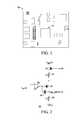
- FIG. 1is a diagram of a Printed Circuit Board (PCB) of an electronic device having one or more integrated circuits according to some embodiments.
- PCBPrinted Circuit Board
- FIG. 2is a diagram of an example of source-follower circuitry according to some embodiments.
- FIG. 3is a diagram of an example of voltage tamper detection circuitry according to some embodiments.
- FIG. 4is a graph illustrating examples of high and low threshold voltages, as well as an out of range signal, against a supply voltage and a “shifted” and “scaled down” supply voltage according to some embodiments.
- FIG. 5is a graph illustrating possible uses of two low threshold voltage values according to some embodiments.
- FIG. 6is a graph illustrating possible uses of two high threshold voltage values according to some embodiments.
- FIG. 7is a flowchart of an example of a method of performing voltage tamper detection according to some embodiments.
- Embodiments disclosed hereinare directed to systems and methods for a low-power voltage tamper detector.
- some of these systems and methodsmay be incorporated into a wide range of devices including, for example, computer systems or Information Technology (IT) products (e.g., servers, desktops, laptops, switches, routers, etc.), telecommunications hardware, consumer devices or appliances (e.g., mobile phones, tablets, televisions, cameras, sound systems, etc.), scientific instrumentation, industrial robotics, medical or laboratory electronics (e.g., imaging, diagnostic, or therapeutic equipment, etc.), transportation vehicles (e.g., automobiles, buses, trains, watercraft, aircraft, etc.), military equipment, or any other device or system having one or more electronic parts or components.
- ITInformation Technology
- such electronic devicesmay include one or more integrated circuits (or “chips”), and each integrated circuit may be provided one or more power supply voltage(s) in order to enable the circuit's operations.
- PCB 100may include one or more electronic component package(s) 101 enclosing one or more integrated circuit(s).
- integrated circuit(s)may include, for instance, System-On-Chips (SoCs), Application Specific Integrated Circuits (ASICs), Digital Signal Processors (DSPs), Field-Programmable Gate Arrays (FPGAs), processors, microprocessors, controllers, microcontrollers (MCUs), and/or the like.
- integrated circuit(s)may include any tangible memory apparatus including, but not limited to, a Random Access Memory (RAM), a Static RAM (SRAM), a Magnetoresistive RAM (MRAM), a Nonvolatile RAM (NVRAM, such as “FLASH” memory, etc.), and/or a Dynamic RAM (DRAM) such as Synchronous DRAM (SDRAM), a Double Data Rate (e.g., DDR, DDR2, DDR3, etc.) RAM, an Erasable Programmable ROM (EPROM), an Electrically Erasable Programmable ROM (EEPROM), etc.
- integrated circuit(s)may include a number of different portions, areas, or regions (e.g., processing cores, cache memories, internal bus(es), timing units, controllers, etc.).
- such integrated circuit(s)may be disposed within electronic component package 101 configured to be mounted onto PCB 100 using any suitable packaging technology (e.g., Ball Grid Array (BGA) packaging).
- PCB 100may include a plurality of other elements or components in addition to component package 101 .
- Integrated circuit(s)are generally designed to work properly so long as its power supply voltage(s) is kept within a specified range of values. If the integrated circuit(s) are subject to conditions outside of its voltage specifications, however, it may make it easier for an intruder, attacker, hacker, etc. to perform an unauthorized use of the circuit's operations and/or information contents (e.g., customer data, etc.). Accordingly, in some cases, an attacker may attempt to purposefully drive the integrated circuit(s) above and/or below the specified ranges of the power supply.
- certain systems and methods described hereinmay detect and prevent illegal use of an integrated circuit(s) out of a specified voltage range.
- a corresponding flagmay be set to alert the integrated circuit(s) (or a user) about the potential threat.
- the integrated circuit(s)may then take an action to enhance the overall system security.
- a low-power voltage tamper detection circuitmay operate in low-power mode (e.g., ⁇ 1 uA) and/or in an extended voltage range.
- systems and methods described hereinmay combine a low-power bandgap circuit with a low-power, reduced area source-follower circuit to generate a scaled down power supply tap voltage that is applied to a high-resistivity P+ poly resistor (thus reducing the circuit area for a specified power consumption target) and then compared against one or more reference voltages.
- both low and high “trip points”may be provided.
- sub-1V voltage reference(s)may be provided in order to promote proper system operation.
- a source-follower circuitmay subtract a bandgap reference voltage (e.g., V bg ⁇ 1.2V) from a power supply voltage (e.g., V dda ), and apply that difference in voltage to a high resistivity P+ polycrystalline silicon resistor (e.g., R 1 ) to result in an electrical current that is equal to (V dda ⁇ V bg )/R 1 .
- a source-follower circuitmay subtract a bandgap reference voltage (e.g., V bg ⁇ 1.2V) from a power supply voltage (e.g., V dda ), and apply that difference in voltage to a high resistivity P+ polycrystalline silicon resistor (e.g., R 1 ) to result in an electrical current that is equal to (V dda ⁇ V bg )/R 1 .
- V dda — SHIFTED[V dd ⁇ V bg ]R 2 R 1 .
- resistor R 1may have to support only (V dda ⁇ V bg ) instead of V dda while resistor R 2 may have to support V dda — SHIFTED .
- FIG. 2is a diagram of an example of source-follower circuitry.
- source-follower circuitry 200may be employed as part of a low-power voltage tamper detection circuit within integrated circuit(s) discussed in connection with FIG. 1 .
- PMOSP-type metal-oxide-semiconductor
- resistor (R 1 ) 204e.g., a high-resistivity P+ polycrystalline silicon or “poly” resistor, or the like
- op-amplow-power operational amplifier
- the non-inverting input of op-amp 206is configured to receive bandgap voltage (V bg ) 205 , and the output of op-amp 206 is configured to drive the gate of PMOS transistor 207 .
- the drain of PMOS transistor 207is connected to resistor R 2 209 to generate the scaled down power supply voltage V dda — SHIFTED 210 , since resistor R 2 209 is tied to the negative power supply (e.g., ground or “Gnd” in FIG. 2 ).
- Capacitor 208is operably coupled to the output of op-amp 206 and to the drain of PMOS transistor 207 . In some implementations, capacitor 208 may be used to add stability to the circuit loop around op-amp 206 ; although stability concerns may also be addressed in other suitable ways.
- V bg 205may be a temperature independent voltage reference with a value of approximately 1.25 V, a value between 1.2V and 1.3V, or another value suitably close to the theoretical 1.22 eV bandgap of silicon at 0 K (i.e., the energy required to promote an electron from its valence band to its conduction band to become a mobile charge).
- a bandgap reference circuitmay provide V bg 205 .
- Such a bandgap reference circuitmay include, for instance, a cascade of Self-Cascode MOS Field-Effect Transistor (SCM) structures and a bipolar transistor operating in an open loop configuration.
- SCMSelf-Cascode MOS Field-Effect Transistor
- source-follower circuitry 200may be configured to subtract V bg 205 from V dda 201 to produce V dda — SHIFTED 210 across R 2 209 .
- V dda — SHIFTED[V dd ⁇ V bg ]R 2 /R 1 .
- R 1 20410 MOhm
- R 2 2092 MOhm
- V dda — SHIFTED 210is 430 mV.
- V dda 201is raised to 3.7 V (e.g., by an attacker attempting to break into the device), then V dda — SHIFTED 210 goes up to 500 mV. Conversely, if V dda 201 is reduced to 1.7 V, V dda — SHIFTED 210 goes down to 100 mV. In other words, as V dda 201 varies between 1.7 and 3.7 V, V dda — SHIFTED 210 varies between 100 and 500 mV, respectively. As such, V dda — SHIFTED 210 is a scaled down voltage with respect to supply voltage V dda 201 .
- V dda — SHIFTED 210may be used by a voltage tamper detection circuit to determine whether V dda 201 has stepped outside of one or more voltage threshold values. For instance, V dda — SHIFTED 210 may be compared with threshold reference voltages value(s) (e.g., 500 mV and 100 mV) to detect when V dda 201 is above 3.7 V or below 1.7 V, respectively.
- threshold reference voltages value(s)e.g., 500 mV and 100 mV
- suitable values for R 1 204 and R 2 209may be selected to produce a desired V dda — SHIFTED 210 given a particular V dda 201 value.
- one or more suitable voltage threshold value(s)may be selected to achieve a desired tampering sensitivity while avoiding false alarms (i.e., an inadvertent detection of tampering in the presence of normal V dda 201 fluctuations).
- FIG. 3is a diagram of an example of voltage tamper detection circuitry.
- voltage tamper detection circuitry 300may be employed as part of a low-power voltage tamper detection circuit within integrated circuit(s) discussed in connection with FIG. 1 .
- an undervoltage detection portion of circuitry 300includes low-power comparator 307 configured to receive V dda — SHIFTED 210 (e.g., from source-follower circuitry 200 of FIG. 2 ) at its inverted input and one of two low voltage threshold values at its non-inverted input.
- low-power comparator 307may receive a first low voltage threshold signal (V ti ) 301 or a second low voltage threshold signal with hysteresis (V ti — h ) 304 through switches 305 and 302 under control of signals V y 306 and V y — b 303 , respectively.
- the output of low-power comparator 307is passed on to inverter 308 , which provides V y — b 303 to inverter 309 .
- Inverter 309then outputs V y 306 , which may be used as one of the inputs of NOR gate 319 .
- an overvoltage detection portion of circuitry 300includes low-power comparator 316 configured to receive V dda — SHIFTED 210 (e.g., from source-follower circuitry 200 of FIG. 2 ) at its inverted input and one of two high voltage threshold values at its non-inverted input.
- low-power comparator 316may receive a first high voltage threshold signal (V th ) 313 or a second high voltage threshold signal with hysteresis (V th — h ) 310 through switches 314 and 311 under control of signals V, 315 and V x — b 312 , respectively.
- the output of low-power comparator 316is passed on to inverter 317 , which provides V xh 312 to inverter 318 .
- Inverter 318outputs V x 315 , which may be used as one of the inputs of NOR gate 319 .
- the over and undervoltage detection portions of circuitry 300may each provide its output (i.e., V x 315 and/or V y 306 , respectively) to NOR gate 319 . If either of V x 315 or V y 306 indicates an over or undervoltage condition, respectively, the output of NOR gate 319 becomes a logic “0,” which is provided to inverter 320 , and which in turn outputs an “out-of-range” signal 321 with a logic “1.” However, if V x 315 does not indicate an overvoltage condition and V y 306 does not indicate an undervoltage condition, respectively, the output of NOR gate 319 becomes a logic “1,” which is provided to inverter 320 , and which in turn outputs an “out-of-range” signal 321 with a logic “0.” In other words, in the example described, “out-of-range” signal 321 may have a logic “1” when indicating an under or over-voltage condition, or a logic “0”
- V th 313 , V th — h 310 , V ti 301 , and/or V ti — h 304may be reference voltage(s) under 1 Volt.
- the same low-power bandgap circuit that provides a temperature independent V bg 205 of FIG. 2may also provide reference voltages V th 313 , V th — h 310 , V ti 301 , and/or V ti — h 304 using a voltage divider (e.g., using a resistor ladder and ladder taps) or the like.
- these sub-1V voltage referencesmay be obtained from an external, low-power sub-1V voltage reference generator unrelated to the bandgap voltage.
- a current reference in the range of a few nAmay be used to provide bias currents for various circuit elements (e.g., op-amp 206 and low-power comparators 307 and 316 ).
- voltage tamper detection circuitry 300is shown with both undervoltage and overvoltage circuit portions, it should be noted that, in some implementations, only the undervoltage circuit portion or only the overvoltage circuit portion may be used. In those situations, either V x 315 or V y 306 may be used as “out-of-range” signal 321 , and logic gates 319 and/or 320 may be absent. It should also be noted that the logic levels selected to indicate an unusual voltage condition are arbitrary. For example, in some cases inverter 320 may be absent, and “out-of-range” signal 321 may indicate normal voltage conditions when its logic value is “1,” and under or overvoltage when its logic value is “0.”
- V ti 301 and V ti — h 304two low threshold voltage levels
- V th 313 and V th — h 310two high threshold voltage levels
- V dda 201Although the noise onto V dda 201 is typically attenuated by capacitances at board and at integrated circuit levels, some noise appears onto V dda — SHIFTED 210 as a small random signal on top of the linear variation of V dda — SHIFTED 210 .
- V ti — h 304may be set higher than V ti 301
- V th — h 310may be set lower than V th 313 , respectively.
- FIG. 4shows a graph illustrating examples of high and low threshold voltages, as well as “out-of-range” signal 321 , against supply voltage V dda 201 and its scaled down version V dda — SHIFTED 210 .
- V ti 301first low threshold voltage
- V th 313first high threshold voltage
- V ti — h 304second low threshold voltage
- V th — h 310second high threshold voltage
- V dda 201is linearly increased from 0 V to an arbitrarily high voltage value, then back to 0 V.
- V dda — SHIFTED 210also varies linearly between 0 V and a scaled down value of the same arbitrarily high voltage.
- V dda 201was 3.3V
- V dda — SHIFTED 210was 430 mV.
- V dda 201was 3.7 V
- V dda — SHIFTED 210was 500 mV.
- V dda 201is reduced to 1.7 V
- V dda — SHIFTED 210is 100 mV.
- V ti 301may be set to 100 mV and V th 313 may be set to 500 mV (as opposed to setting V ti 301 to 1.7 V and V th 313 to 3.7 V).
- V dda — SHIFTED 210When V dda — SHIFTED 210 is operating between V ti 301 and V th 313 (i.e., V dda 201 is lower than 3.7 V and higher than 1.7 V), no undervoltage or overvoltage condition occurs.
- Trip points 401 - 404indicate when V dda — SHIFTED 210 , and by implication V dda 201 , are operating out of range.
- V dda — SHIFTED 210is 100 mV or less (i.e., V dda 201 is 1.7 V or less), and out-of-range signal 321 , shown in the bottom part of graph 400 , is at a logic “1;” here indicating an undervoltage condition.
- V dda — SHIFTED 210is greater than 100 mV but smaller than 500 mV (i.e., V dda 201 is between 1.7 V and 3.7 V), and out-of-range signal 321 is at a logic “0,” thus indicating normal operation.
- V dda — SHIFTED 210is equal to or greater than 500 mV (i.e., V dda 201 is 3.7 V or greater), and out-of-range signal 321 is at a logic “1;” here indicating an overvoltage condition.
- an integrated circuit employing voltage tamper detection circuitry 300may be configured to take predetermined actions in response to out-of-range signal 321 indicating voltage tampering or the like.
- the integrated circuitmay block a memory area, erase the memory area, disallow a number of processing operations, block communications with other components (e.g., over a communications bus or the like), etc.
- the predetermined actionmay be different depending upon the tampering is detected as an undervoltage or overvoltage condition. For instance, if the integrated circuit is known to be more easily attacked when supplied with an overvoltage, the predetermined action in that situation may be more severe than another predetermined action implemented as part of an undervoltage detection (or vice-versa).
- two or more undervoltage detection circuitseach with a different low threshold voltage value may be used.
- different levels of undervoltage detectionmay be associated with different predetermined actions (e.g., when V dda 201 drops below a certain voltage level, a moderate preventive measure is implemented, and when V dda 201 drops further below an even lower voltage level, a more aggressive measure may be implemented).
- two or more overvoltage detection circuitseach with a different high threshold voltage value may be used.
- different levels of overvoltage detectionmay be associated with different predetermined actions (e.g., when V dda 201 rises above a certain voltage level, a moderate preventive measure is implemented, and when V dda 201 increases further above an even higher voltage level, a more aggressive measure may be implemented).
- V dda — SHIFTED 210is close to 100 mV against V ti 301 at 100 mV
- some amount of hysteresismay be added to undervoltage detection portion of circuitry 300 by including V ti — h 304 .
- FIG. 5is a graph illustrating a possible operation of the two low threshold voltages (V ti 301 and V ti — h 304 ) according to some embodiments.
- graph 500may be seen as a “zoomed in” portion of graph 400 of FIG. 4 in the neighborhood of trip point 404 .
- V dda — SHIFTED 210is greater than V ti — h 304 and V ti 301 in region 501 .
- the output of low-power comparator 307is a logic low (“0”)
- V y — b 303is a logic high (“1”)
- V y 306is a logic low.
- switch 302is turned on and switch 305 is turned off—that is, the comparison being made is between V dda — SHIFTED 210 and V ti 301 .
- the situationremains unchanged when V dda — SHIFTED 210 goes further down into region 404 —that is, V dda — SHIFTED 210 is lower than V ti — h 304 but higher than V ti 301 .
- V dda — SHIFTED 210When V dda — SHIFTED 210 reaches V ti 301 at the lower end of region 404 , V dda — SHIFTED 210 is lower than both V ti — h 304 and V ti 301 . Then, the output of low-power comparator 307 goes to a logic high, V y — b 303 goes to a logic low, and V y 306 goes to a logic high. Thus, switch 302 is turned off, and switch 305 is turned on—that is, the comparison being made is now between V dda — SHIFTED 210 and V ti — h 304 .
- V dda — SHIFTED 210is lower than both V ti — h 304 and V ti 301 , and V th — h 304 is higher than V th 301 , the circuit condition remains the same. Electrical noise coming from V dda 201 and coupled onto V dda — SHIFTED 210 with some attenuation does not change the output of low-power comparator 307 , provided that the difference between V ti — h 304 and V ti 301 is larger than that noise. In some embodiments, such a hysteresis voltage may be set to produce a ⁇ 100 mV guard band in terms of V dda 201 .
- V dda 201goes up and V dda — SHIFTED 210 rises (in a scaled down factor) above V ti — h 304 , the output of low-power comparator 307 changes to a logic low, so circuitry 300 again indicates normal operation regarding power supply V dda 201 .
- V dda 201may be at 1.8 V or above to be in normal operation.
- overvoltage detection portion of circuitry 300may include V th — h 310 .
- FIG. 6is a graph illustrating a possible operation of the two high threshold voltages (V th 313 and V th — h 310 ) according to some embodiments.
- graph 600may be seen as a “zoomed in” portion of graph 400 of FIG. 4 in the neighborhood of trip point 402 .
- V dda — SHIFTED 210is smaller than both V th — h 313 and V th — h 310 in region 602 .
- the output of the low power comparator 316is a logic high (“1”)
- V x — b 312is a logic low (“0”)
- V x 315is a logic high.
- switch 311is turned off and switch 314 is turned on—that is, the comparison being made is between V dda — SHIFTED 210 and V th 313 .
- the conditionremains the same when V dda — SHIFTED 210 further goes up and is in region 402 —that is, V dda — SHIFTED 210 is higher than V th — h 310 but lower than V th 313 .
- V dda — SHIFTED 210When V dda — SHIFTED 210 reaches V th 313 at the higher end of region 402 , V dda — SHIFTED 210 is higher than both V th — h 310 and V th 313 . Then, the output of the low-power comparator 316 is a logic low, V x — b 312 is a logic high, and V x 315 is a logic low. Thus, switch 311 is turned on and switch 314 is turned off—that is, the comparison being made is now between V dda — SHIFTED 210 and V th — h 310 .
- V dda — SHIFTED 210is higher than both V th — h 310 and V th 313 , and V th 313 is higher than V th — h 310 , the condition remains the same.
- the noise coming from V dda 201 and coupled onto V dda — SHIFTED 210 with some attenuationdoes not change the output of low-power comparator 316 , provided that the difference between V th 313 and V th — h 310 is larger than that noise.
- the hysteresis voltagemay be set to provide a 100 mV guard band in terms of V dda 201 .
- V dda 201goes down and V dda — SHIFTED 210 also decreases (in a scaled down factor) below V th — h 310 , the output of the low power comparator 316 changes to a logic low, and circuitry 300 again indicates normal operation regarding power supply V dda 201 .
- V dda 201may be at 3.6 V or below to be in normal operation.
- V th — h 313 and V th — h 310may be within a few millivolts, or a few tens of millivolts of each other.
- V ti 301 and V th — h 304may also be within a few millivolts, or within a few tens of millivolts of each other.
- FIG. 7is a flowchart of an example of a method of performing voltage tamper detection.
- method 700may be performed, at least in part, by voltage tamper detection circuitry 300 of FIG. 3 in conjunction with the source-follower circuitry 200 of FIG. 2 .
- method 700may include subtracting a bandgap reference voltage (e.g., V bg 205 ) from a power supply voltage (e.g., V dda 201 ) and multiplying the difference by a factor smaller than 1 to produce a scaled down power supply voltage (e.g., V dda — SHIFTED 210 ).
- a bandgap reference voltagee.g., V bg 205
- V dda 201power supply voltage
- V dda — SHIFTED 210a scaled down power supply voltage
- method 700may include determining whether the scaled power supply voltage is greater than one or more high threshold voltages. If so, method 700 may include generating an “out of range” signal (e.g., “out_of_range” signal 321 is set at a logic high) at block 705 . Otherwise, method 700 may include generating a “within range” signal (e.g., “out_of_range” signal 323 is set at a logic low) at block 704 . Additionally or alternatively, at block 703 , method 700 may include determining whether the scaled power supply voltage is smaller than one or more low threshold voltages.
- an “out of range” signale.g., “out_of_range” signal 321 is set at a logic high
- method 700may include generating a “within range” signal (e.g., “out_of_range” signal 323 is set at a logic low) at block 704 .
- method 700may include determining whether the scaled power supply voltage is smaller than one or more low threshold voltages
- method 700may include generating the “out of range” signal (e.g., “out_of_range” signal 323 is set at a logic high) at block 705 . Otherwise, method 700 may include generating the “within range” signal (e.g., “out_of_range” signal 323 is set at a logic low) at block 704 .
- the “out of range” signale.g., “out_of_range” signal 323 is set at a logic high
- method 700may include generating the “within range” signal (e.g., “out_of_range” signal 323 is set at a logic low) at block 704 .
- the use of source-follower circuitry 200may uniquely satisfy a number of design parameters such as, for example: low power consumption, temperature stability, small area, good noise immunity, and/or high precision. In some cases, two or more of these parameters may be satisfied simultaneously. In other cases, all of these requirements may be satisfied simultaneously.
- the use of source-follower circuitry 200may, in some instances, reduce or eliminate the need for a power hungry bandgap or reference voltage continuously enabled, thus further promoting low power operation.
- the use of one or more high resistivity P+ poly resistors 204 / 209may also reduce or minimize silicon area for a given power consumption.
- the use of sub-1V voltage reference(s) V th 313 , V th — h 310 , V ti 301 , and/or V ti — h 304may further reduce the overall power consumption.
- an integrated circuitmay include source-follower circuitry configured to produce a scaled down supply voltage, and undervoltage detection circuitry operably coupled to the source-follower circuitry, the undervoltage detection circuitry configured to output a first signal having a first logic value in response to the scaled down supply voltage being greater than a low threshold voltage or a second logic value in response to the scaled down supply voltage being smaller than the low threshold voltage.
- the source-follower circuitrymay include two or more resistors and it may be configured to subtract a bandgap voltage from a supply voltage to produce the scaled down supply voltage.
- the low threshold voltagemay be 1 Volt or less.
- the undervoltage detection circuitrymay be further configured to compare the scaled down supply voltage with a first low threshold voltage value in response to the scaled down supply voltage being greater than the first low threshold voltage value. Additionally or alternatively, the undervoltage detection circuitry may be further configured to compare the scaled down supply voltage with a second low threshold voltage value in response to the scaled down supply voltage being equal to or smaller than the first low threshold voltage value, the second low threshold voltage value being greater than the first low threshold voltage value.
- the integrated circuitmay include overvoltage detection circuitry operably coupled to the source-follower circuitry, the overvoltage detection circuitry configured to output a second signal having the first logic value in response to the scaled down supply voltage being smaller than a high threshold voltage or the second logic value in response to the scaled down supply voltage being greater than the high threshold voltage.
- the integrated circuitmay further include logic circuitry operably coupled to the undervoltage detection circuitry and to the overvoltage detection circuitry, the logic circuitry configured to output an out-of-range signal in response to at least one of the first or second signals having the second logic level.
- an integrated circuitmay include source-follower circuitry configured to produce a scaled down supply voltage, and overvoltage detection circuitry operably coupled to the source-follower circuitry, the overvoltage detection circuitry configured to output a first signal having a first logic value in response to the scaled down supply voltage being smaller than a high threshold voltage or a second logic value in response to the scaled down supply voltage being greater than the high threshold voltage.
- the source-follower circuitrymay include two or more resistors and it may be configured to subtract a bandgap voltage from a supply voltage to produce the scaled down supply voltage.
- the high threshold voltagemay be 1 Volt or less.
- the overvoltage detection circuitrymay be configured to compare the scaled down supply voltage with a first high threshold voltage value in response to the scaled down supply voltage being smaller than the first high threshold voltage value. Additionally or alternatively, the overvoltage detection circuitry may be configured to compare the scaled down supply voltage with a second high threshold voltage value in response to the scaled down supply voltage being equal to or greater than the first high threshold voltage value, the second high threshold voltage value being smaller than the first high threshold voltage value.
- the integrated circuitmay include undervoltage detection circuitry operably coupled to the source-follower circuitry, the undervoltage detection circuitry configured to output a second signal having the first logic value in response to the scaled down supply voltage being greater than a low threshold voltage or the second logic value in response to the scaled down supply voltage being smaller than the low threshold voltage.
- the integrated circuitmay further include logic circuitry operably coupled to the overvoltage detection circuitry and to the undervoltage detection circuitry, the logic circuitry configured to output an out-of-range signal in response to at least one of the first or second signals having the second logic level.
- a methodmay include subtracting a bandgap reference voltage from a power supply voltage to produce a scaled power supply voltage, and at least one of: (a) generating a first signal having a first logic level response to the scaled power supply voltage being greater than a low threshold voltage or having a second logic level in response to the scaled power supply voltage being smaller than the low threshold voltage or (b) generating a second signal having the first logic value in response to the scaled power supply voltage being smaller than a high threshold voltage or the second logic value in response to the scaled power supply voltage being greater than the high threshold voltage.
- the methodmay further include producing an out-of-range signal in response to at least one of the first or second signals having the second logic level.
- the methodmay also include making a comparison between the scaled power supply voltage and a first low threshold value or a second low threshold value based, at least in part, upon a result of a previous comparison between the scaled power supply voltage and the first low threshold value. For example, the method may include comparing the scaled power supply voltage with a first low threshold voltage value if the scaled power supply voltage is greater than the first low threshold value and comparing the scaled power supply voltage with a second low threshold value if to the scaled power supply voltage is equal to or smaller than the first low threshold value, the second low threshold value being greater than the first low threshold value.
- the methodmay include making a comparison between the scaled power supply voltage and a first high threshold value or a second high threshold value based, at least in part, upon a result of a previous comparison between the scaled power supply voltage and the first high threshold value. For example, the method may include comparing the scaled power supply voltage with a first high threshold voltage value if the scaled power supply voltage is smaller than the first high threshold voltage value and comparing the scaled power supply voltage with a second high threshold voltage value if the scaled power supply voltage is equal to or greater than the first high threshold voltage value, the first high threshold voltage value being greater than the second high threshold voltage value.
Landscapes
- Engineering & Computer Science (AREA)
- Physics & Mathematics (AREA)
- General Physics & Mathematics (AREA)
- Theoretical Computer Science (AREA)
- Power Engineering (AREA)
- Electromagnetism (AREA)
- Radar, Positioning & Navigation (AREA)
- Automation & Control Theory (AREA)
- General Engineering & Computer Science (AREA)
- Measurement Of Current Or Voltage (AREA)
- Emergency Protection Circuit Devices (AREA)
Abstract
Description
Claims (18)
Priority Applications (1)
| Application Number | Priority Date | Filing Date | Title |
|---|---|---|---|
| US13/681,956US8988114B2 (en) | 2012-11-20 | 2012-11-20 | Low-power voltage tamper detection |
Applications Claiming Priority (1)
| Application Number | Priority Date | Filing Date | Title |
|---|---|---|---|
| US13/681,956US8988114B2 (en) | 2012-11-20 | 2012-11-20 | Low-power voltage tamper detection |
Publications (2)
| Publication Number | Publication Date |
|---|---|
| US20140139201A1 US20140139201A1 (en) | 2014-05-22 |
| US8988114B2true US8988114B2 (en) | 2015-03-24 |
Family
ID=50727342
Family Applications (1)
| Application Number | Title | Priority Date | Filing Date |
|---|---|---|---|
| US13/681,956Active2033-07-10US8988114B2 (en) | 2012-11-20 | 2012-11-20 | Low-power voltage tamper detection |
Country Status (1)
| Country | Link |
|---|---|
| US (1) | US8988114B2 (en) |
Cited By (3)
| Publication number | Priority date | Publication date | Assignee | Title |
|---|---|---|---|---|
| US10474846B1 (en)* | 2017-08-31 | 2019-11-12 | Square, Inc. | Processor power supply glitch detection |
| US20210370287A1 (en)* | 2018-05-10 | 2021-12-02 | Halliburton Energy Services, Inc. | Tamper-Resistant Pressurized Well Fluid Transfer Bottle Having Sensor Package, Memory Gauge and Display and Uses Thereof |
| US20220011351A1 (en)* | 2020-04-01 | 2022-01-13 | Shenzhen GOODIX Technology Co., Ltd. | Voltage attack detection circuit and chip |
Families Citing this family (2)
| Publication number | Priority date | Publication date | Assignee | Title |
|---|---|---|---|---|
| US10664031B2 (en)* | 2016-11-26 | 2020-05-26 | Arm Limited | Monitoring circuit and method |
| KR102801225B1 (en)* | 2021-01-14 | 2025-04-30 | 삼성전자주식회사 | Low voltage attack detector |
Citations (25)
| Publication number | Priority date | Publication date | Assignee | Title |
|---|---|---|---|---|
| US4013902A (en) | 1975-08-06 | 1977-03-22 | Honeywell Inc. | Initial reset signal generator and low voltage detector |
| US4301380A (en) | 1979-05-01 | 1981-11-17 | Motorola, Inc. | Voltage detector |
| US4766567A (en) | 1984-04-19 | 1988-08-23 | Ltd. Nippondenso Co. | One-chip data processing device including low voltage detector |
| US5187389A (en) | 1991-05-03 | 1993-02-16 | National Semiconductor Corporation | Noise resistant low voltage brownout detector with shut off option |
| US5196833A (en) | 1991-08-13 | 1993-03-23 | Ford Motor Company | Low voltage detector circuit |
| US5199032A (en) | 1990-09-04 | 1993-03-30 | Motorola, Inc. | Microcontroller having an EPROM with a low voltage program inhibit circuit |
| US5396118A (en)* | 1992-08-27 | 1995-03-07 | Kabushiki Kaisha Riken | Pressure detector circuit |
| US5440263A (en) | 1992-04-30 | 1995-08-08 | Sgs-Thomson Microelectronics, S.A. | Voltage threshold detection circuit with very low power consumption |
| US5457748A (en) | 1992-11-30 | 1995-10-10 | Motorola, Inc. | Method and apparatus for improved security within encrypted communication devices |
| US5495453A (en) | 1994-10-19 | 1996-02-27 | Intel Corporation | Low power voltage detector circuit including a flash memory cell |
| US5619156A (en) | 1995-08-29 | 1997-04-08 | Motorola, Inc. | Low voltage inhibit circuit and integrated circuit using same |
| US5814995A (en) | 1996-09-12 | 1998-09-29 | Telcom Semiconductor, Inc. | Voltage detector for battery operated device |
| US5903767A (en) | 1988-12-09 | 1999-05-11 | Dallas Semiconductor Corporation | Integrated circuit for providing supervisory functions to a microprocessor |
| US5920182A (en) | 1997-08-21 | 1999-07-06 | Stmicroelectronics S.A. | "Reset" type power supply voltage monitoring device |
| US6002290A (en)* | 1997-12-23 | 1999-12-14 | Sarnoff Corporation | Crisscross voltage level shifter |
| US6559692B2 (en)* | 1998-04-24 | 2003-05-06 | Cirrus Logic, Inc. | Output driver for a 10baset/100basetx ethernet physical layer line interface |
| US6559629B1 (en) | 2001-07-09 | 2003-05-06 | Cygnal Integrated Products, Inc. | Supply voltage monitor using bandgap device without feedback |
| US6646508B1 (en)* | 1996-12-30 | 2003-11-11 | Anthony T. Barbetta | Wide bandwidth, current sharing, MOSFET audio power amplifier with multiple feedback loops |
| US6661218B2 (en) | 2000-12-30 | 2003-12-09 | Hynix Semiconductor Inc | High voltage detector |
| US20070103234A1 (en)* | 2005-09-28 | 2007-05-10 | Yamaha Corporation | Class D amplifier |
| US7274226B2 (en) | 2004-03-31 | 2007-09-25 | Nec Electronics Corporation | Power source voltage monitoring circuit for self-monitoring its power source voltage |
| US20080122539A1 (en)* | 2006-05-16 | 2008-05-29 | Fujitsu Limited | Signal amplification device |
| US7839189B2 (en) | 2008-12-19 | 2010-11-23 | Freescale Semiconductor, Inc. | Voltage detector device and methods thereof |
| US20120139633A1 (en)* | 2010-07-30 | 2012-06-07 | Panasonic Corporation | Semiconductor integrated circuit and tuner system including the same |
| US20130027007A1 (en)* | 2011-07-27 | 2013-01-31 | Fujitsu Semiconductor Limited | Amplifier with multiple zero-pole pairs |
- 2012
- 2012-11-20USUS13/681,956patent/US8988114B2/enactiveActive
Patent Citations (27)
| Publication number | Priority date | Publication date | Assignee | Title |
|---|---|---|---|---|
| US4013902A (en) | 1975-08-06 | 1977-03-22 | Honeywell Inc. | Initial reset signal generator and low voltage detector |
| US4301380A (en) | 1979-05-01 | 1981-11-17 | Motorola, Inc. | Voltage detector |
| US4766567A (en) | 1984-04-19 | 1988-08-23 | Ltd. Nippondenso Co. | One-chip data processing device including low voltage detector |
| US5903767A (en) | 1988-12-09 | 1999-05-11 | Dallas Semiconductor Corporation | Integrated circuit for providing supervisory functions to a microprocessor |
| US5199032A (en) | 1990-09-04 | 1993-03-30 | Motorola, Inc. | Microcontroller having an EPROM with a low voltage program inhibit circuit |
| US5187389A (en) | 1991-05-03 | 1993-02-16 | National Semiconductor Corporation | Noise resistant low voltage brownout detector with shut off option |
| US5196833A (en) | 1991-08-13 | 1993-03-23 | Ford Motor Company | Low voltage detector circuit |
| US5619165A (en) | 1992-04-30 | 1997-04-08 | Sgs-Thomson Microelectronics, S.A. | Voltage threshold detection circuit with very low consumption |
| US5440263A (en) | 1992-04-30 | 1995-08-08 | Sgs-Thomson Microelectronics, S.A. | Voltage threshold detection circuit with very low power consumption |
| US5396118A (en)* | 1992-08-27 | 1995-03-07 | Kabushiki Kaisha Riken | Pressure detector circuit |
| US5457748A (en) | 1992-11-30 | 1995-10-10 | Motorola, Inc. | Method and apparatus for improved security within encrypted communication devices |
| US5495453A (en) | 1994-10-19 | 1996-02-27 | Intel Corporation | Low power voltage detector circuit including a flash memory cell |
| US5619156A (en) | 1995-08-29 | 1997-04-08 | Motorola, Inc. | Low voltage inhibit circuit and integrated circuit using same |
| US5814995A (en) | 1996-09-12 | 1998-09-29 | Telcom Semiconductor, Inc. | Voltage detector for battery operated device |
| US6646508B1 (en)* | 1996-12-30 | 2003-11-11 | Anthony T. Barbetta | Wide bandwidth, current sharing, MOSFET audio power amplifier with multiple feedback loops |
| US5920182A (en) | 1997-08-21 | 1999-07-06 | Stmicroelectronics S.A. | "Reset" type power supply voltage monitoring device |
| US6002290A (en)* | 1997-12-23 | 1999-12-14 | Sarnoff Corporation | Crisscross voltage level shifter |
| US6559692B2 (en)* | 1998-04-24 | 2003-05-06 | Cirrus Logic, Inc. | Output driver for a 10baset/100basetx ethernet physical layer line interface |
| US6661218B2 (en) | 2000-12-30 | 2003-12-09 | Hynix Semiconductor Inc | High voltage detector |
| US6559629B1 (en) | 2001-07-09 | 2003-05-06 | Cygnal Integrated Products, Inc. | Supply voltage monitor using bandgap device without feedback |
| US7274226B2 (en) | 2004-03-31 | 2007-09-25 | Nec Electronics Corporation | Power source voltage monitoring circuit for self-monitoring its power source voltage |
| US20070103234A1 (en)* | 2005-09-28 | 2007-05-10 | Yamaha Corporation | Class D amplifier |
| US20090115514A1 (en)* | 2005-09-28 | 2009-05-07 | Yamaha Corporation | Class D amplifier |
| US20080122539A1 (en)* | 2006-05-16 | 2008-05-29 | Fujitsu Limited | Signal amplification device |
| US7839189B2 (en) | 2008-12-19 | 2010-11-23 | Freescale Semiconductor, Inc. | Voltage detector device and methods thereof |
| US20120139633A1 (en)* | 2010-07-30 | 2012-06-07 | Panasonic Corporation | Semiconductor integrated circuit and tuner system including the same |
| US20130027007A1 (en)* | 2011-07-27 | 2013-01-31 | Fujitsu Semiconductor Limited | Amplifier with multiple zero-pole pairs |
Cited By (4)
| Publication number | Priority date | Publication date | Assignee | Title |
|---|---|---|---|---|
| US10474846B1 (en)* | 2017-08-31 | 2019-11-12 | Square, Inc. | Processor power supply glitch detection |
| US20210370287A1 (en)* | 2018-05-10 | 2021-12-02 | Halliburton Energy Services, Inc. | Tamper-Resistant Pressurized Well Fluid Transfer Bottle Having Sensor Package, Memory Gauge and Display and Uses Thereof |
| US20220011351A1 (en)* | 2020-04-01 | 2022-01-13 | Shenzhen GOODIX Technology Co., Ltd. | Voltage attack detection circuit and chip |
| US11940471B2 (en)* | 2020-04-01 | 2024-03-26 | Shenzhen GOODIX Technology Co., Ltd. | Voltage attack detection circuit and chip |
Also Published As
| Publication number | Publication date |
|---|---|
| US20140139201A1 (en) | 2014-05-22 |
Similar Documents
| Publication | Publication Date | Title |
|---|---|---|
| US8988114B2 (en) | Low-power voltage tamper detection | |
| US7859421B2 (en) | Circuit and method for detecting a voltage change | |
| US9472510B2 (en) | Semiconductor device and control system | |
| US9275718B2 (en) | Semiconductor devices with periodic signal generation circuits and semiconductor systems including the same | |
| US10164426B2 (en) | Sensing and detection of ESD and other transient overstress events | |
| US10211620B2 (en) | Semiconductor device | |
| US9092043B2 (en) | Power switch with current limitation and zero direct current (DC) power consumption | |
| CN112673263A (en) | Burr signal detection circuit, safety chip and electronic equipment | |
| US8736333B1 (en) | Schmitt trigger circuit with near rail-to-rail hysteresis | |
| US8183897B2 (en) | Integrated circuit device and electronic apparatus | |
| US9141119B2 (en) | Reducing output voltage ripple of power supplies | |
| US10998276B2 (en) | Integrated circuit | |
| US8729951B1 (en) | Voltage ramp-up protection | |
| US9092045B2 (en) | Startup circuits with native transistors | |
| US10564213B2 (en) | Dielectric breakdown monitor | |
| US9644593B2 (en) | Cold-crank event management | |
| KR20100079071A (en) | Circuit for power on | |
| KR102628843B1 (en) | power failure detection circuit | |
| US9509305B2 (en) | Power gating techniques with smooth transition | |
| US20200400726A1 (en) | Voltage threshold sensing systems and related methods | |
| US9110484B2 (en) | Temperature dependent biasing for leakage power reduction | |
| US11125787B2 (en) | Semiconductor device and semiconductor system comprising the same | |
| US9153959B2 (en) | Phase detection circuit | |
| US9202584B1 (en) | Power supply slew rate detector | |
| US10063225B1 (en) | Voltage switching device and method |
Legal Events
| Date | Code | Title | Description |
|---|---|---|---|
| AS | Assignment | Owner name:FREESCALE SEMICONDUCTOR, INC., TEXAS Free format text:ASSIGNMENT OF ASSIGNORS INTEREST;ASSIGNORS:WADHWA, SANJAY K.;OLMOS, ALFREDO;DE MARTIN, FABIO DUARTE;SIGNING DATES FROM 20121031 TO 20121107;REEL/FRAME:029330/0252 | |
| AS | Assignment | Owner name:CITIBANK, N.A., AS NOTES COLLATERAL AGENT, NEW YORK Free format text:SUPPLEMENT TO IP SECURITY AGREEMENT;ASSIGNOR:FREESCALE SEMICONDUCTOR, INC.;REEL/FRAME:030258/0558 Effective date:20130214 Owner name:CITIBANK, N.A., AS NOTES COLLATERAL AGENT, NEW YORK Free format text:SUPPLEMENT TO IP SECURITY AGREEMENT;ASSIGNOR:FREESCALE SEMICONDUCTOR, INC.;REEL/FRAME:030258/0523 Effective date:20130214 Owner name:CITIBANK, N.A., AS NOTES COLLATERAL AGENT, NEW YOR Free format text:SUPPLEMENT TO IP SECURITY AGREEMENT;ASSIGNOR:FREESCALE SEMICONDUCTOR, INC.;REEL/FRAME:030258/0523 Effective date:20130214 Owner name:CITIBANK, N.A., AS NOTES COLLATERAL AGENT, NEW YOR Free format text:SUPPLEMENT TO IP SECURITY AGREEMENT;ASSIGNOR:FREESCALE SEMICONDUCTOR, INC.;REEL/FRAME:030258/0558 Effective date:20130214 Owner name:CITIBANK, N.A., AS COLLATERAL AGENT, NEW YORK Free format text:SUPPLEMENT TO IP SECURITY AGREEMENT;ASSIGNOR:FREESCALE SEMICONDUCTOR, INC.;REEL/FRAME:030258/0540 Effective date:20130214 | |
| AS | Assignment | Owner name:CITIBANK, N.A., AS NOTES COLLATERAL AGENT, NEW YORK Free format text:SECURITY AGREEMENT;ASSIGNOR:FREESCALE SEMICONDUCTOR, INC.;REEL/FRAME:030633/0424 Effective date:20130521 Owner name:CITIBANK, N.A., AS NOTES COLLATERAL AGENT, NEW YOR Free format text:SECURITY AGREEMENT;ASSIGNOR:FREESCALE SEMICONDUCTOR, INC.;REEL/FRAME:030633/0424 Effective date:20130521 | |
| AS | Assignment | Owner name:CITIBANK, N.A., AS NOTES COLLATERAL AGENT, NEW YORK Free format text:SECURITY AGREEMENT;ASSIGNOR:FREESCALE SEMICONDUCTOR, INC.;REEL/FRAME:031591/0266 Effective date:20131101 Owner name:CITIBANK, N.A., AS NOTES COLLATERAL AGENT, NEW YOR Free format text:SECURITY AGREEMENT;ASSIGNOR:FREESCALE SEMICONDUCTOR, INC.;REEL/FRAME:031591/0266 Effective date:20131101 | |
| FEPP | Fee payment procedure | Free format text:PAYOR NUMBER ASSIGNED (ORIGINAL EVENT CODE: ASPN); ENTITY STATUS OF PATENT OWNER: LARGE ENTITY | |
| STCF | Information on status: patent grant | Free format text:PATENTED CASE | |
| AS | Assignment | Owner name:FREESCALE SEMICONDUCTOR, INC., TEXAS Free format text:PATENT RELEASE;ASSIGNOR:CITIBANK, N.A., AS COLLATERAL AGENT;REEL/FRAME:037357/0685 Effective date:20151207 Owner name:FREESCALE SEMICONDUCTOR, INC., TEXAS Free format text:PATENT RELEASE;ASSIGNOR:CITIBANK, N.A., AS COLLATERAL AGENT;REEL/FRAME:037357/0671 Effective date:20151207 | |
| AS | Assignment | Owner name:MORGAN STANLEY SENIOR FUNDING, INC., MARYLAND Free format text:ASSIGNMENT AND ASSUMPTION OF SECURITY INTEREST IN PATENTS;ASSIGNOR:CITIBANK, N.A.;REEL/FRAME:037486/0517 Effective date:20151207 | |
| AS | Assignment | Owner name:MORGAN STANLEY SENIOR FUNDING, INC., MARYLAND Free format text:ASSIGNMENT AND ASSUMPTION OF SECURITY INTEREST IN PATENTS;ASSIGNOR:CITIBANK, N.A.;REEL/FRAME:037518/0292 Effective date:20151207 | |
| AS | Assignment | Owner name:FREESCALE SEMICONDUCTOR, INC., TEXAS Free format text:PATENT RELEASE;ASSIGNOR:CITIBANK, N.A., AS COLLATERAL AGENT;REEL/FRAME:037494/0312 Effective date:20151207 | |
| AS | Assignment | Owner name:MORGAN STANLEY SENIOR FUNDING, INC., MARYLAND Free format text:SECURITY AGREEMENT SUPPLEMENT;ASSIGNOR:NXP B.V.;REEL/FRAME:038017/0058 Effective date:20160218 | |
| AS | Assignment | Owner name:MORGAN STANLEY SENIOR FUNDING, INC., MARYLAND Free format text:SUPPLEMENT TO THE SECURITY AGREEMENT;ASSIGNOR:FREESCALE SEMICONDUCTOR, INC.;REEL/FRAME:039138/0001 Effective date:20160525 | |
| AS | Assignment | Owner name:MORGAN STANLEY SENIOR FUNDING, INC., MARYLAND Free format text:CORRECTIVE ASSIGNMENT TO CORRECT THE REMOVE APPLICATION 12092129 PREVIOUSLY RECORDED ON REEL 038017 FRAME 0058. ASSIGNOR(S) HEREBY CONFIRMS THE SECURITY AGREEMENT SUPPLEMENT;ASSIGNOR:NXP B.V.;REEL/FRAME:039361/0212 Effective date:20160218 | |
| AS | Assignment | Owner name:NXP, B.V., F/K/A FREESCALE SEMICONDUCTOR, INC., NETHERLANDS Free format text:RELEASE BY SECURED PARTY;ASSIGNOR:MORGAN STANLEY SENIOR FUNDING, INC.;REEL/FRAME:040925/0001 Effective date:20160912 Owner name:NXP, B.V., F/K/A FREESCALE SEMICONDUCTOR, INC., NE Free format text:RELEASE BY SECURED PARTY;ASSIGNOR:MORGAN STANLEY SENIOR FUNDING, INC.;REEL/FRAME:040925/0001 Effective date:20160912 | |
| AS | Assignment | Owner name:NXP B.V., NETHERLANDS Free format text:RELEASE BY SECURED PARTY;ASSIGNOR:MORGAN STANLEY SENIOR FUNDING, INC.;REEL/FRAME:040928/0001 Effective date:20160622 | |
| AS | Assignment | Owner name:NXP USA, INC., TEXAS Free format text:MERGER;ASSIGNOR:FREESCALE SEMICONDUCTOR, INC.;REEL/FRAME:041144/0363 Effective date:20161107 | |
| AS | Assignment | Owner name:MORGAN STANLEY SENIOR FUNDING, INC., MARYLAND Free format text:CORRECTIVE ASSIGNMENT TO CORRECT THE REMOVE PATENTS 8108266 AND 8062324 AND REPLACE THEM WITH 6108266 AND 8060324 PREVIOUSLY RECORDED ON REEL 037518 FRAME 0292. ASSIGNOR(S) HEREBY CONFIRMS THE ASSIGNMENT AND ASSUMPTION OF SECURITY INTEREST IN PATENTS;ASSIGNOR:CITIBANK, N.A.;REEL/FRAME:041703/0536 Effective date:20151207 | |
| AS | Assignment | Owner name:MORGAN STANLEY SENIOR FUNDING, INC., MARYLAND Free format text:CORRECTIVE ASSIGNMENT TO CORRECT THE REMOVE APPLICATION 12681366 PREVIOUSLY RECORDED ON REEL 039361 FRAME 0212. ASSIGNOR(S) HEREBY CONFIRMS THE SECURITY AGREEMENT SUPPLEMENT;ASSIGNOR:NXP B.V.;REEL/FRAME:042762/0145 Effective date:20160218 Owner name:MORGAN STANLEY SENIOR FUNDING, INC., MARYLAND Free format text:CORRECTIVE ASSIGNMENT TO CORRECT THE REMOVE APPLICATION 12681366 PREVIOUSLY RECORDED ON REEL 038017 FRAME 0058. ASSIGNOR(S) HEREBY CONFIRMS THE SECURITY AGREEMENT SUPPLEMENT;ASSIGNOR:NXP B.V.;REEL/FRAME:042985/0001 Effective date:20160218 | |
| MAFP | Maintenance fee payment | Free format text:PAYMENT OF MAINTENANCE FEE, 4TH YEAR, LARGE ENTITY (ORIGINAL EVENT CODE: M1551) Year of fee payment:4 | |
| AS | Assignment | Owner name:SHENZHEN XINGUODU TECHNOLOGY CO., LTD., CHINA Free format text:CORRECTIVE ASSIGNMENT TO CORRECT THE TO CORRECT THE APPLICATION NO. FROM 13,883,290 TO 13,833,290 PREVIOUSLY RECORDED ON REEL 041703 FRAME 0536. ASSIGNOR(S) HEREBY CONFIRMS THE THE ASSIGNMENT AND ASSUMPTION OF SECURITYINTEREST IN PATENTS.;ASSIGNOR:MORGAN STANLEY SENIOR FUNDING, INC.;REEL/FRAME:048734/0001 Effective date:20190217 | |
| AS | Assignment | Owner name:NXP B.V., NETHERLANDS Free format text:RELEASE BY SECURED PARTY;ASSIGNOR:MORGAN STANLEY SENIOR FUNDING, INC.;REEL/FRAME:050744/0097 Effective date:20190903 Owner name:NXP B.V., NETHERLANDS Free format text:RELEASE BY SECURED PARTY;ASSIGNOR:MORGAN STANLEY SENIOR FUNDING, INC.;REEL/FRAME:050745/0001 Effective date:20190903 | |
| AS | Assignment | Owner name:MORGAN STANLEY SENIOR FUNDING, INC., MARYLAND Free format text:CORRECTIVE ASSIGNMENT TO CORRECT THE REMOVE APPLICATION 12298143 PREVIOUSLY RECORDED ON REEL 042762 FRAME 0145. ASSIGNOR(S) HEREBY CONFIRMS THE SECURITY AGREEMENT SUPPLEMENT;ASSIGNOR:NXP B.V.;REEL/FRAME:051145/0184 Effective date:20160218 Owner name:MORGAN STANLEY SENIOR FUNDING, INC., MARYLAND Free format text:CORRECTIVE ASSIGNMENT TO CORRECT THE REMOVE APPLICATION 12298143 PREVIOUSLY RECORDED ON REEL 039361 FRAME 0212. ASSIGNOR(S) HEREBY CONFIRMS THE SECURITY AGREEMENT SUPPLEMENT;ASSIGNOR:NXP B.V.;REEL/FRAME:051029/0387 Effective date:20160218 Owner name:MORGAN STANLEY SENIOR FUNDING, INC., MARYLAND Free format text:CORRECTIVE ASSIGNMENT TO CORRECT THE REMOVE APPLICATION 12298143 PREVIOUSLY RECORDED ON REEL 042985 FRAME 0001. ASSIGNOR(S) HEREBY CONFIRMS THE SECURITY AGREEMENT SUPPLEMENT;ASSIGNOR:NXP B.V.;REEL/FRAME:051029/0001 Effective date:20160218 Owner name:MORGAN STANLEY SENIOR FUNDING, INC., MARYLAND Free format text:CORRECTIVE ASSIGNMENT TO CORRECT THE REMOVE APPLICATION12298143 PREVIOUSLY RECORDED ON REEL 042985 FRAME 0001. ASSIGNOR(S) HEREBY CONFIRMS THE SECURITY AGREEMENT SUPPLEMENT;ASSIGNOR:NXP B.V.;REEL/FRAME:051029/0001 Effective date:20160218 Owner name:MORGAN STANLEY SENIOR FUNDING, INC., MARYLAND Free format text:CORRECTIVE ASSIGNMENT TO CORRECT THE REMOVE APPLICATION12298143 PREVIOUSLY RECORDED ON REEL 039361 FRAME 0212. ASSIGNOR(S) HEREBY CONFIRMS THE SECURITY AGREEMENT SUPPLEMENT;ASSIGNOR:NXP B.V.;REEL/FRAME:051029/0387 Effective date:20160218 Owner name:MORGAN STANLEY SENIOR FUNDING, INC., MARYLAND Free format text:CORRECTIVE ASSIGNMENT TO CORRECT THE REMOVE APPLICATION 12298143 PREVIOUSLY RECORDED ON REEL 038017 FRAME 0058. ASSIGNOR(S) HEREBY CONFIRMS THE SECURITY AGREEMENT SUPPLEMENT;ASSIGNOR:NXP B.V.;REEL/FRAME:051030/0001 Effective date:20160218 Owner name:MORGAN STANLEY SENIOR FUNDING, INC., MARYLAND Free format text:CORRECTIVE ASSIGNMENT TO CORRECT THE REMOVE APPLICATION12298143 PREVIOUSLY RECORDED ON REEL 042762 FRAME 0145. ASSIGNOR(S) HEREBY CONFIRMS THE SECURITY AGREEMENT SUPPLEMENT;ASSIGNOR:NXP B.V.;REEL/FRAME:051145/0184 Effective date:20160218 | |
| AS | Assignment | Owner name:MORGAN STANLEY SENIOR FUNDING, INC., MARYLAND Free format text:CORRECTIVE ASSIGNMENT TO CORRECT THE REMOVE APPLICATION11759915 AND REPLACE IT WITH APPLICATION 11759935 PREVIOUSLY RECORDED ON REEL 037486 FRAME 0517. ASSIGNOR(S) HEREBY CONFIRMS THE ASSIGNMENT AND ASSUMPTION OF SECURITYINTEREST IN PATENTS;ASSIGNOR:CITIBANK, N.A.;REEL/FRAME:053547/0421 Effective date:20151207 | |
| AS | Assignment | Owner name:NXP B.V., NETHERLANDS Free format text:CORRECTIVE ASSIGNMENT TO CORRECT THE REMOVEAPPLICATION 11759915 AND REPLACE IT WITH APPLICATION11759935 PREVIOUSLY RECORDED ON REEL 040928 FRAME 0001. ASSIGNOR(S) HEREBY CONFIRMS THE RELEASE OF SECURITYINTEREST;ASSIGNOR:MORGAN STANLEY SENIOR FUNDING, INC.;REEL/FRAME:052915/0001 Effective date:20160622 | |
| AS | Assignment | Owner name:NXP, B.V. F/K/A FREESCALE SEMICONDUCTOR, INC., NETHERLANDS Free format text:CORRECTIVE ASSIGNMENT TO CORRECT THE REMOVEAPPLICATION 11759915 AND REPLACE IT WITH APPLICATION11759935 PREVIOUSLY RECORDED ON REEL 040925 FRAME 0001. ASSIGNOR(S) HEREBY CONFIRMS THE RELEASE OF SECURITYINTEREST;ASSIGNOR:MORGAN STANLEY SENIOR FUNDING, INC.;REEL/FRAME:052917/0001 Effective date:20160912 | |
| MAFP | Maintenance fee payment | Free format text:PAYMENT OF MAINTENANCE FEE, 8TH YEAR, LARGE ENTITY (ORIGINAL EVENT CODE: M1552); ENTITY STATUS OF PATENT OWNER: LARGE ENTITY Year of fee payment:8 |