US8987874B2 - Microelectronic workpieces and methods for manufacturing microelectronic devices using such workpieces - Google Patents
Microelectronic workpieces and methods for manufacturing microelectronic devices using such workpiecesDownload PDFInfo
- Publication number
- US8987874B2 US8987874B2US13/948,025US201313948025AUS8987874B2US 8987874 B2US8987874 B2US 8987874B2US 201313948025 AUS201313948025 AUS 201313948025AUS 8987874 B2US8987874 B2US 8987874B2
- Authority
- US
- United States
- Prior art keywords
- projection
- microelectronic
- substrate
- conductive
- bond sites
- Prior art date
- Legal status (The legal status is an assumption and is not a legal conclusion. Google has not performed a legal analysis and makes no representation as to the accuracy of the status listed.)
- Active
Links
Images


Classifications
- H—ELECTRICITY
- H01—ELECTRIC ELEMENTS
- H01L—SEMICONDUCTOR DEVICES NOT COVERED BY CLASS H10
- H01L21/00—Processes or apparatus adapted for the manufacture or treatment of semiconductor or solid state devices or of parts thereof
- H—ELECTRICITY
- H01—ELECTRIC ELEMENTS
- H01L—SEMICONDUCTOR DEVICES NOT COVERED BY CLASS H10
- H01L23/00—Details of semiconductor or other solid state devices
- H01L23/28—Encapsulations, e.g. encapsulating layers, coatings, e.g. for protection
- H01L23/31—Encapsulations, e.g. encapsulating layers, coatings, e.g. for protection characterised by the arrangement or shape
- H—ELECTRICITY
- H01—ELECTRIC ELEMENTS
- H01L—SEMICONDUCTOR DEVICES NOT COVERED BY CLASS H10
- H01L21/00—Processes or apparatus adapted for the manufacture or treatment of semiconductor or solid state devices or of parts thereof
- H01L21/02—Manufacture or treatment of semiconductor devices or of parts thereof
- H01L21/04—Manufacture or treatment of semiconductor devices or of parts thereof the devices having potential barriers, e.g. a PN junction, depletion layer or carrier concentration layer
- H01L21/50—Assembly of semiconductor devices using processes or apparatus not provided for in a single one of the groups H01L21/18 - H01L21/326 or H10D48/04 - H10D48/07 e.g. sealing of a cap to a base of a container
- H01L21/56—Encapsulations, e.g. encapsulation layers, coatings
- H01L21/563—Encapsulation of active face of flip-chip device, e.g. underfilling or underencapsulation of flip-chip, encapsulation preform on chip or mounting substrate
- H—ELECTRICITY
- H01—ELECTRIC ELEMENTS
- H01L—SEMICONDUCTOR DEVICES NOT COVERED BY CLASS H10
- H01L23/00—Details of semiconductor or other solid state devices
- H01L23/12—Mountings, e.g. non-detachable insulating substrates
- H01L23/13—Mountings, e.g. non-detachable insulating substrates characterised by the shape
- H—ELECTRICITY
- H01—ELECTRIC ELEMENTS
- H01L—SEMICONDUCTOR DEVICES NOT COVERED BY CLASS H10
- H01L24/00—Arrangements for connecting or disconnecting semiconductor or solid-state bodies; Methods or apparatus related thereto
- H01L24/93—Batch processes
- H01L24/95—Batch processes at chip-level, i.e. with connecting carried out on a plurality of singulated devices, i.e. on diced chips
- H01L24/96—Batch processes at chip-level, i.e. with connecting carried out on a plurality of singulated devices, i.e. on diced chips the devices being encapsulated in a common layer, e.g. neo-wafer or pseudo-wafer, said common layer being separable into individual assemblies after connecting
- B—PERFORMING OPERATIONS; TRANSPORTING
- B33—ADDITIVE MANUFACTURING TECHNOLOGY
- B33Y—ADDITIVE MANUFACTURING, i.e. MANUFACTURING OF THREE-DIMENSIONAL [3-D] OBJECTS BY ADDITIVE DEPOSITION, ADDITIVE AGGLOMERATION OR ADDITIVE LAYERING, e.g. BY 3-D PRINTING, STEREOLITHOGRAPHY OR SELECTIVE LASER SINTERING
- B33Y80/00—Products made by additive manufacturing
- H—ELECTRICITY
- H01—ELECTRIC ELEMENTS
- H01L—SEMICONDUCTOR DEVICES NOT COVERED BY CLASS H10
- H01L2224/00—Indexing scheme for arrangements for connecting or disconnecting semiconductor or solid-state bodies and methods related thereto as covered by H01L24/00
- H01L2224/01—Means for bonding being attached to, or being formed on, the surface to be connected, e.g. chip-to-package, die-attach, "first-level" interconnects; Manufacturing methods related thereto
- H01L2224/02—Bonding areas; Manufacturing methods related thereto
- H01L2224/04—Structure, shape, material or disposition of the bonding areas prior to the connecting process
- H01L2224/05—Structure, shape, material or disposition of the bonding areas prior to the connecting process of an individual bonding area
- H01L2224/0554—External layer
- H01L2224/0556—Disposition
- H01L2224/0557—Disposition the external layer being disposed on a via connection of the semiconductor or solid-state body
- H—ELECTRICITY
- H01—ELECTRIC ELEMENTS
- H01L—SEMICONDUCTOR DEVICES NOT COVERED BY CLASS H10
- H01L2224/00—Indexing scheme for arrangements for connecting or disconnecting semiconductor or solid-state bodies and methods related thereto as covered by H01L24/00
- H01L2224/01—Means for bonding being attached to, or being formed on, the surface to be connected, e.g. chip-to-package, die-attach, "first-level" interconnects; Manufacturing methods related thereto
- H01L2224/02—Bonding areas; Manufacturing methods related thereto
- H01L2224/04—Structure, shape, material or disposition of the bonding areas prior to the connecting process
- H01L2224/05—Structure, shape, material or disposition of the bonding areas prior to the connecting process of an individual bonding area
- H01L2224/0554—External layer
- H01L2224/0556—Disposition
- H01L2224/05571—Disposition the external layer being disposed in a recess of the surface
- H—ELECTRICITY
- H01—ELECTRIC ELEMENTS
- H01L—SEMICONDUCTOR DEVICES NOT COVERED BY CLASS H10
- H01L2224/00—Indexing scheme for arrangements for connecting or disconnecting semiconductor or solid-state bodies and methods related thereto as covered by H01L24/00
- H01L2224/01—Means for bonding being attached to, or being formed on, the surface to be connected, e.g. chip-to-package, die-attach, "first-level" interconnects; Manufacturing methods related thereto
- H01L2224/02—Bonding areas; Manufacturing methods related thereto
- H01L2224/04—Structure, shape, material or disposition of the bonding areas prior to the connecting process
- H01L2224/05—Structure, shape, material or disposition of the bonding areas prior to the connecting process of an individual bonding area
- H01L2224/0554—External layer
- H01L2224/05573—Single external layer
- H—ELECTRICITY
- H01—ELECTRIC ELEMENTS
- H01L—SEMICONDUCTOR DEVICES NOT COVERED BY CLASS H10
- H01L2224/00—Indexing scheme for arrangements for connecting or disconnecting semiconductor or solid-state bodies and methods related thereto as covered by H01L24/00
- H01L2224/01—Means for bonding being attached to, or being formed on, the surface to be connected, e.g. chip-to-package, die-attach, "first-level" interconnects; Manufacturing methods related thereto
- H01L2224/10—Bump connectors; Manufacturing methods related thereto
- H01L2224/12—Structure, shape, material or disposition of the bump connectors prior to the connecting process
- H01L2224/14—Structure, shape, material or disposition of the bump connectors prior to the connecting process of a plurality of bump connectors
- H01L2224/141—Disposition
- H01L2224/1412—Layout
- H01L2224/1415—Mirror array, i.e. array having only a reflection symmetry, i.e. bilateral symmetry
- H01L2224/14154—Mirror array, i.e. array having only a reflection symmetry, i.e. bilateral symmetry covering only portions of the surface to be connected
- H01L2224/14156—Covering only the central area of the surface to be connected, i.e. central arrangements
- H—ELECTRICITY
- H01—ELECTRIC ELEMENTS
- H01L—SEMICONDUCTOR DEVICES NOT COVERED BY CLASS H10
- H01L2224/00—Indexing scheme for arrangements for connecting or disconnecting semiconductor or solid-state bodies and methods related thereto as covered by H01L24/00
- H01L2224/73—Means for bonding being of different types provided for in two or more of groups H01L2224/10, H01L2224/18, H01L2224/26, H01L2224/34, H01L2224/42, H01L2224/50, H01L2224/63, H01L2224/71
- H01L2224/732—Location after the connecting process
- H01L2224/73201—Location after the connecting process on the same surface
- H01L2224/73203—Bump and layer connectors
- H01L2224/73204—Bump and layer connectors the bump connector being embedded into the layer connector
- H—ELECTRICITY
- H01—ELECTRIC ELEMENTS
- H01L—SEMICONDUCTOR DEVICES NOT COVERED BY CLASS H10
- H01L2224/00—Indexing scheme for arrangements for connecting or disconnecting semiconductor or solid-state bodies and methods related thereto as covered by H01L24/00
- H01L2224/80—Methods for connecting semiconductor or other solid state bodies using means for bonding being attached to, or being formed on, the surface to be connected
- H01L2224/81—Methods for connecting semiconductor or other solid state bodies using means for bonding being attached to, or being formed on, the surface to be connected using a bump connector
- H01L2224/8119—Arrangement of the bump connectors prior to mounting
- H01L2224/81191—Arrangement of the bump connectors prior to mounting wherein the bump connectors are disposed only on the semiconductor or solid-state body
- H—ELECTRICITY
- H01—ELECTRIC ELEMENTS
- H01L—SEMICONDUCTOR DEVICES NOT COVERED BY CLASS H10
- H01L2924/00—Indexing scheme for arrangements or methods for connecting or disconnecting semiconductor or solid-state bodies as covered by H01L24/00
- H01L2924/0001—Technical content checked by a classifier
- H01L2924/00014—Technical content checked by a classifier the subject-matter covered by the group, the symbol of which is combined with the symbol of this group, being disclosed without further technical details
- H—ELECTRICITY
- H01—ELECTRIC ELEMENTS
- H01L—SEMICONDUCTOR DEVICES NOT COVERED BY CLASS H10
- H01L2924/00—Indexing scheme for arrangements or methods for connecting or disconnecting semiconductor or solid-state bodies as covered by H01L24/00
- H01L2924/01—Chemical elements
- H01L2924/01046—Palladium [Pd]
- H—ELECTRICITY
- H01—ELECTRIC ELEMENTS
- H01L—SEMICONDUCTOR DEVICES NOT COVERED BY CLASS H10
- H01L2924/00—Indexing scheme for arrangements or methods for connecting or disconnecting semiconductor or solid-state bodies as covered by H01L24/00
- H01L2924/01—Chemical elements
- H01L2924/01078—Platinum [Pt]
- H—ELECTRICITY
- H01—ELECTRIC ELEMENTS
- H01L—SEMICONDUCTOR DEVICES NOT COVERED BY CLASS H10
- H01L2924/00—Indexing scheme for arrangements or methods for connecting or disconnecting semiconductor or solid-state bodies as covered by H01L24/00
- H01L2924/01—Chemical elements
- H01L2924/01079—Gold [Au]
- H—ELECTRICITY
- H01—ELECTRIC ELEMENTS
- H01L—SEMICONDUCTOR DEVICES NOT COVERED BY CLASS H10
- H01L2924/00—Indexing scheme for arrangements or methods for connecting or disconnecting semiconductor or solid-state bodies as covered by H01L24/00
- H01L2924/10—Details of semiconductor or other solid state devices to be connected
- H01L2924/11—Device type
- H01L2924/14—Integrated circuits
- H—ELECTRICITY
- H01—ELECTRIC ELEMENTS
- H01L—SEMICONDUCTOR DEVICES NOT COVERED BY CLASS H10
- H01L2924/00—Indexing scheme for arrangements or methods for connecting or disconnecting semiconductor or solid-state bodies as covered by H01L24/00
- H01L2924/15—Details of package parts other than the semiconductor or other solid state devices to be connected
- H01L2924/151—Die mounting substrate
- H01L2924/156—Material
- H01L2924/15786—Material with a principal constituent of the material being a non metallic, non metalloid inorganic material
- H01L2924/15787—Ceramics, e.g. crystalline carbides, nitrides or oxides
- H—ELECTRICITY
- H01—ELECTRIC ELEMENTS
- H01L—SEMICONDUCTOR DEVICES NOT COVERED BY CLASS H10
- H01L2924/00—Indexing scheme for arrangements or methods for connecting or disconnecting semiconductor or solid-state bodies as covered by H01L24/00
- H01L2924/15—Details of package parts other than the semiconductor or other solid state devices to be connected
- H01L2924/181—Encapsulation
- H—ELECTRICITY
- H01—ELECTRIC ELEMENTS
- H01L—SEMICONDUCTOR DEVICES NOT COVERED BY CLASS H10
- H01L2924/00—Indexing scheme for arrangements or methods for connecting or disconnecting semiconductor or solid-state bodies as covered by H01L24/00
- H01L2924/30—Technical effects
- H01L2924/301—Electrical effects
- H01L2924/30105—Capacitance
Definitions
- the present disclosureis related to microelectronic workpieces and methods for manufacturing microelectronic devices using such workpieces.
- Semiconductor devices and other types of microelectronic devicescan include a microelectronic die attached to a ceramic chip carrier, organic printed circuit board, lead frame, or other type of interposing structure.
- the diescan be attached to interposing structures using Direct Chip Attach (DCA), flip-chip bonding, or wire-bonding to electrically connect the integrated circuitry in the dies to the wiring of the interposing structures.
- DCA or flip-chip methodsfor example, include depositing very small bumps or balls of a conductive material (e.g., solder) onto the contacts of a die. The bumps are then connected to corresponding contacts or pads on an interposing structure.
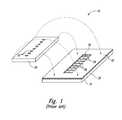
- FIG. 1is a partially schematic, isometric illustration of a portion of a conventional flip-chip assembly 10 including a microelectronic die 20 positioned for attachment to a substrate 30 .
- the die 20includes a plurality of conductive bumps 22 arranged in an array along an active side of the die 20 .
- the substrate 30includes a front surface 31 and a dielectric mask or layer 32 carried by the front surface 31 .
- the dielectric mask 32includes an aperture or opening 34 extending lengthwise along a medial portion of the mask 32 .
- the substrate 30also includes a plurality of contacts or traces 36 located at the front surface 31 and arranged in a pattern corresponding at least in part to the arrangement of conductive bumps 22 on the die 20 .
- a solder ball 38 or other conductive coupleris disposed on each contact 36 .
- the contacts 36 and solder balls 38are accessible through the aperture 34 for coupling to corresponding conductive bumps 22 . More specifically, during attachment the die 20 is inverted or “flipped” such that the active side bearing the conductive bumps 22 is superimposed with corresponding solder balls 38 and/or contacts 36 on the substrate 30 , and a suitable reflow process is used to electrically and mechanically connect the die 20 to the substrate 30 .
- An underfill material(not shown) may then be disposed in the gap between the die 20 and substrate 30 to protect the components from environmental factors (e.g., moisture, particulates, static electricity, and physical impact) and to enhance the mechanical attachment of the die 20 to the substrate 30 .
- the underfill materialis typically dispensed into the gap by injecting the underfill material along one or two sides of the flip-chip device, and the underfill material is drawn into the gap by capillary effects.
- One potential drawback with the foregoing approachis that it may result in a vulnerable mechanical connection between the die 20 and the substrate 30 .
- air bubbles, air pockets, and/or voidsmay form within the underfill material.
- the trench region around the aperture 34is particularly susceptible to such voids because of the large volume of underfill material required to fill this area. During subsequent high temperature processes, the air trapped in these regions may expand and force the die 20 away from the substrate 30 , damaging the mechanical and/or electrical connections between these components.
- Another drawback with this approachis that the underfilling method may be very time-consuming because the relatively large gap between the die 20 and substrate 30 takes time to fill, and the volume of fill material in the gap takes time to cure. This can significantly increase the overall time required for manufacturing the assembly.
- solder balls 38may make contact with the corresponding conductive bumps 22 of the die 20 .
- the solder balls 38must typically be fairly large (e.g., about 80 ⁇ m) to extend between the bumps 22 and the corresponding contacts 36 .
- some of the solder balls 38may be misshapen or smaller than normal and, accordingly, a gap may exist between these solder balls 38 and the corresponding conductive bumps 22 . During the reflow process, this gap may not seal and the result may be an open circuit between the die's conductive bump 22 and the corresponding solder ball 38 and contact 36 .
- FIG. 1is a partially schematic, isometric illustration of a conventional flip-chip assembly configured in accordance with one aspect of the prior art.
- FIG. 2Ais partially schematic, isometric illustration of a portion of a microelectronic workpiece configured in accordance with an embodiment of the invention.
- FIG. 2Bis a side cross-sectional view taken substantially along line 2 B- 2 B of FIG. 2A with a microelectronic die attached to the workpiece.
- FIGS. 3A-3Cillustrate stages in a method for forming a microelectronic workpiece configured in accordance with an embodiment of the invention.
- FIGS. 4A-4Cillustrate stages in a method for forming a microelectronic workpiece configured in accordance with another embodiment of the invention.
- FIG. 5is a partially schematic, side cross-sectional view of a microelectronic workpiece configured in accordance with still another embodiment of the invention.
- FIG. 6is a schematic illustration of a system in which the microelectronic workpiece may be incorporated.
- microelectronic devices described belowinclude a single microelectronic die attached to a support member, but in other embodiments the microelectronic devices can have two or more stacked microelectronic dies electrically coupled to a support member.
- the microelectronic devicescan include, for example, micromechanical components, data storage elements, optics, read/write components, or other features.
- the microelectronic diescan be SRAM, DRAM (e.g., DDR-SDRAM), flash-memory (e.g., NAND flash-memory), processors, imagers, and other types of devices.
- Substratescan be semiconductive pieces (e.g., doped silicon wafers, gallium arsenide wafers, or other semiconductor wafers), non-conductive pieces (e.g., various ceramic substrates), or conductive pieces.
- semiconductive piecese.g., doped silicon wafers, gallium arsenide wafers, or other semiconductor wafers
- non-conductive piecese.g., various ceramic substrates
- conductive piecese.g., various ceramic substrates
- several other embodiments of the inventioncan have configurations, components, or procedures different than those described in this section. A person of ordinary skill in the art, therefore, will accordingly understand that the invention may have other embodiments with additional elements, or the invention may have other embodiments without several of the elements shown and described below with reference to FIGS. 2A-6 .
- FIG. 2Ais partially schematic, isometric illustration of a portion of a microelectronic workpiece 100 configured in accordance with an embodiment of the invention. More specifically, FIG. 2A illustrates the workpiece 100 at an intermediate processing stage before a semiconductor component has been attached to the workpiece 100 . In previous processing steps, a number of structures have been formed on and/or in the workpiece 100 .
- the workpiece 100can include a substrate 110 having a first side 112 , a projection or ridge 116 extending away from the first side 112 , and a plurality of conductive traces 120 disposed on and/or in the substrate 110 . One or more conductive traces 120 extend over or are otherwise carried by the projection 116 .
- the conductive traces 120are conductive lines arranged in a desired pattern on the substrate 110 and configured to transmit signals to and/or from one or more external devices attached to the workpiece 100 .
- the workpiece 100further includes a protective coating or layer 130 (e.g., a solder mask) disposed on the substrate 110 and over at least a portion of the conductive traces 120 .
- the protective coating 130has an outer (e.g., upper) surface 132 at a desired distance from the first side 112 of the substrate 110 .
- the outer surface 132can be formed at a distance from the first side 112 corresponding at least in part to the height of the projection 116 such that the outer surface 132 is approximately co-planar or flush with an outer surface 121 of the one or more portions of the conductive traces 120 (shown in FIG. 2A as exposed conductive bond sites or trace portions 120 a ) carried by the projection 116 .
- FIG. 2Bis a side cross-sectional view of the workpiece 100 taken substantially along line 2 B- 2 B of FIG. 2A at a subsequent processing stage in which a microelectronic die 140 has been physically and electrically coupled to corresponding conductive traces 120 of the workpiece 100 in a flip-chip configuration to form a packaged microelectronic device 190 .
- the die 140can be a processor, a memory device (e.g., a DRAM or flash memory device), an imager, a sensor, a filter, or other type of microelectronic device.
- the die 140can include integrated circuitry 142 (shown schematically), a plurality of terminals 144 (only one is shown in broken lines) electrically coupled to the integrated circuitry 142 , and a plurality of conductive bumps or stud bumps 146 projecting from corresponding terminals 144 .
- the conductive bumps 146are configured to engage the exposed bond sites 120 a at the outer surface 132 of the protective coating 130 to electrically and physically couple the die 140 to the workpiece 100 .
- the device 190can further include an underfill material 160 disposed between the die 140 and the workpiece 100 to help attach the die 140 to the workpiece 100 and to protect the conductive bumps 146 and corresponding bond sites 120 a from contamination (e.g., moisture, particulates, etc.).
- contaminatione.g., moisture, particulates, etc.
- the outer surface 132 of the protective coating 130is approximately co-planar or flush with the outer surfaces 121 of the bond sites 120 a on the projection 116 .
- the generally planar surface across the entire upper portion of the workpiece 100reduces or eliminates the chances for air bubbles, air pockets, and/or voids to form within the underfill material 160 because there are no large cavities or open spaces on the upper surface of the workpiece 100 that require excessive amounts of underfill material 160 .
- the likelihood of voids in the underfill material 160is also reduced.
- microelectronic device 190may provide improved package reliability and robustness as compared with conventional flip-chip devices.
- the air trapped in voids or cavities within the underfill material in conventional flip-chip assembliescan expand and force the die away from the substrate, damaging the mechanical and/or electrical connections between these components. This in turn often leads to failure or malfunction of such devices.
- the generally planar upper surface of the workpiece 100significantly reduces the likelihood that such voids may form, thereby reducing and/or eliminating the tendency for the mechanical and/or electrical connections in the device 190 to fail.
- An embodiment of the microelectronic device 190 described above with reference to FIGS. 2A and 2Bincludes a support member 110 having a first side 112 and a projection 116 extending away from the first side 112 .
- the device 190also includes a plurality of conductive traces 120 at the first side 112 of the support member 110 . Some of the conductive traces 120 include bond sites 120 a carried by the projection 116 and having an outer surface 121 at a first distance from the first side 112 of the support member 110 .
- the device 190further includes a protective coating 130 deposited over the first side 112 of the support member 110 and at least a portion of the conductive traces 120 .
- the protective coating 130has a major outer surface 132 at a second distance from the first side 112 of the support member 110 .
- the second distanceis approximately the same as the first distance such that the outer surface 132 of the protective coating 130 is generally co-planar with the outer surface 121 of the bond sites 120 a carried by the projection 116 .
- FIGS. 3A-5 described belowillustrate various embodiments of microelectronic workpieces and methods for forming such workpieces. Although the following description does not show the workpieces attached to semiconductor components (e.g., microelectronic dies) or other external devices, it will be appreciated that the workpieces described below can be electrically and physically coupled to a variety of different semiconductor components.
- FIGS. 3A-3Cillustrate stages in a method for forming the microelectronic workpiece 100 in accordance with an embodiment of the invention.
- FIG. 3Ais a partially schematic, isometric view of the workpiece 100 at an initial stage before any external materials have been deposited on or otherwise attached to the substrate 110 .
- the substrate 110can include the first side 112 and a second side 114 facing opposite the first side 112 .
- the substrate 110can include an interposer substrate, a printed circuit board, a lead frame, or another suitable support member.
- the substrate 110can be composed of polymeric materials (e.g., resins, silicones, etc.), organic materials other than polymeric materials, or other suitable non-ceramic dielectric materials.
- the selection of a material for the substrate 110for example, can be based on the particular application(s) for which the resulting microelectronic device will be used.
- the projection 116was formed at the first side 112 of the substrate 110 .
- the projection 116is a ridge or stand-off extending lengthwise along a medial portion of the substrate 110 .
- the projection 116is an integral component of the substrate 110 and is composed of the same material as the substrate 110 .
- the projection 116may not be integral with the substrate 110 and/or may be composed of a different material than the substrate 110 , as described in greater detail below with reference to FIGS. 4A-4C .
- the projection 116can be formed at the first side 112 using a stamping process, a compression molding process, a deposition process, or another suitable technique.
- the projection 116can have a variety of different shapes and configurations based, at least in part, upon the configuration of a device or component to be attached to the workpiece 100 , the material of which the substrate 110 is composed, and/or the desired configuration of conductive traces (not shown) upon the substrate 110 .
- the height of the projection 116can vary depending upon the particular configuration (e.g., thickness, etc.) of the conductive traces (not shown) disposed on the substrate 110 .
- a conductive (e.g., metal) layer 124is deposited onto the first side 114 of the substrate 110 and patterned and etched to form the conductive traces 120 .
- the conductive layer 124can be composed of Cu, Au, Ag, Al, Pd, and/or another suitable material or combination of materials having the desired properties.
- the conductive layer 124can be applied onto the substrate 110 using a variety of different techniques (e.g., stamping, physical vapor deposition (PVD), plating, chemical vapor deposition (CVD), etc.) depending on the composition of the material and/or the configuration of the substrate 110 .
- the conductive traces 120are conductive lines that are arranged on the substrate 110 in a variety of different patterns, and can be formed on and/or in the first side 112 of the substrate and over the projection 116 .
- the conductive traces 120 in FIG. 2Bare shown as a series of generally parallel strips or ridges, and include a plurality of interstitial regions between the individual traces. In other embodiments, however, the conductive traces 120 can have a variety of other configurations and/or arrangements on the substrate 110 .
- FIG. 3Cis a side cross-sectional view illustrating a portion of the workpiece 100 after the protective coating 130 (e.g., solder mask) is formed at the first side 112 of the substrate 110 .
- the protective coating 130is typically composed of a dielectric material and may be deposited onto the substrate 110 using deposition processes (e.g., CVD or PVD), three-dimensional stereolithography processes, spin-on techniques, spraying techniques, molding, or other processes. Referring to FIGS.
- the protective coating 130can (a) fill the interstitial regions between the individual conductive traces 120 to electrically insulate each trace 120 , and (b) cover the exposed portions of the first side 112 of the substrate 110 and the conductive traces 120 and protect them from environmental factors (e.g., moisture, particulates, physical damage, etc.).
- the protective coating 130has an outer surface 132 at a desired distance from the first side 112 of the substrate 110 .
- the outer surface 132can be formed at a precise distance from the first side 112 by planarizing the protective coating 130 using chemical-mechanical planarization or another suitable grinding process. In several embodiments, however, the outer surface 132 can be formed at the desired distance from the substrate 130 in the deposition process without planarizing or grinding the protective coating 130 .
- the projection 116 and the bond sites 120 acombine to have a height H above the front side 112 of the substrate 110 .
- the protective coating 130is accordingly formed with a corresponding thickness T such that the outer surface 132 of the protective coating 130 is approximately co-planar or flush with the outer surface 121 of the bond sites 120 a .
- the workpiece 100has a generally uniform cross-sectional dimension across the entire workpiece 100 , and there are no large cavities, trenches, or depressions in the upper surface of the workpiece 100 .
- the protective layer 130may have an outer surface 132 a (shown in broken lines) slightly recessed or below the outer surface 121 of the bond sites 120 a .
- the outer surface 132 ais not precisely co-planar with the outer surface 121 in such instances, there is not a substantial difference between the two surfaces.
- the upper surface across the entire workpiece 100is generally planar and does not include any large cavities or openings that may require significant amounts of underfill material.
- the term “generally planar”can be defined as (a) substantially planar and/or (b) having some minor deviation from planarity (e.g., within the thickness of the individual bond sites 120 a ).
- FIGS. 4A-4Cillustrate stages in a method for forming a microelectronic workpiece configured in accordance with another embodiment of the invention.
- FIG. 4Ais a partially schematic, side cross-sectional view of a workpiece 200 at an initial stage of the process.
- the workpiece 200can include a substrate 210 having a first side 212 and a second side 214 facing opposite the first side 212 .
- the substrate 210can be composed of materials similar to the substrate 110 discussed above with reference to FIG. 3A . In other embodiments, however, the substrate 210 can be composed of other materials.
- the substrate 210differs from the substrate 110 described above with reference to FIG. 3A in that the substrate 210 does not include an integral projection, like the projection 116 of the substrate 110 . Rather, as discussed below, a projection is formed on the substrate 210 using materials different from the material of which the substrate 210 is composed.
- a conductive layer 220was deposited onto the first side 212 of the substrate 210 .
- the conductive layer 220can include Cu, Au, Ag, Al, Pd or other suitable conductive materials.
- the conductive layer 220can be deposited onto the substrate 210 using processes similar to those used to deposit the conductive layer 124 described above with reference to FIG. 3B .
- a first mask 222is applied over the conductive layer 220 and patterned as shown in FIG. 4A .
- the first mask 222can be a layer of resist or another suitable photo-active material that is patterned according to the desired configuration of a projection or ridge to be formed on the substrate, as described in greater detail below.
- the conductive layer 220is etched using a first etching process to form a projection or ridge 216 at a medial portion of the substrate 210 .
- the projection 216can have similar dimensions to the projection 116 described above with reference to FIGS. 2A-3C .
- an outer (e.g., upper) surface 217 of the projection 216can have a distance from the first side 212 of the substrate 210 similar to the distance between an outer surface of the projection 116 and the first side 112 of the substrate 110 (as best seen in FIG. 2B ).
- the projection 216can have different dimensions and/or a different configuration.
- a second mask 224is applied over the conductive layer 220 and patterned.
- the second mask 224can be patterned according to a desired arrangement of (a) conductive traces or lines at the first side 212 of the substrate 210 , and (b) conductive bond sites on the projection 216 .
- the conductive layer 220is etched using a second etching process to form a plurality of conductive traces 226 on the substrate 210 and a plurality of bond sites 226 a on the projection 216 .
- the second etching processselectively removes material from the conductive layer 220 , but not the substrate 210 .
- the substrate 210can accordingly act as an etch-stop for the second etching process.
- a protective coating or layer 230(e.g., a solder mask) is deposited onto the workpiece 200 and over the conductive traces 226 .
- the protective coating 230can be generally similar to the protective coating 130 described above.
- the protective coating 230can include an outer surface 232 formed at a precise distance from the first side 212 of the substrate 210 using a planarization process or another suitable technique such that the outer surface 232 is generally co-planar with the outer surface 217 of the projection 216 .
- the workpiece 200accordingly has a generally planar, smooth upper surface that does not include any large openings, recesses, or cavities.
- FIG. 5is a partially schematic, side cross-sectional view of a microelectronic workpiece 300 configured in accordance with still another embodiment of the invention.
- the workpiece 300differs from the workpieces 100 and 200 described above in that the workpiece 300 includes one or more conductive couplers or elements 302 (only one is shown) attached to corresponding bond sites or trace portions 120 a .
- the conductive couplers 302can include, for example, gold bumps or “pikes,” solder balls, conductive paste, or another suitable conductive element.
- the conductive couplers 302are optional elements that may not be included in some embodiments.
- a microelectronic die or other semiconductor componentcan be attached to the workpiece 200 ( FIG. 4C ) or the workpiece 300 in a flip-chip configuration.
- any one of the packaged microelectronic devices described above with reference to FIGS. 2A-5can be incorporated into any of a myriad of larger and/or more complex systems, a representative example of which is a system 600 shown schematically in FIG. 6 .
- the system 600can include a processor 602 , a memory 604 (e.g., SRAM, DRAM, flash, and/or other memory device), input/output devices 606 , and/or other subsystems or components 608 .
- the microelectronic devices described above with reference to FIGS. 2A-5may be included in any of the components shown in FIG. 6 .
- the resulting system 600can perform any of a wide variety of computing, processing, storage, sensing, imaging, and/or other functions.
- representative systems 600include, without limitation, computers and/or other data processors, for example, desktop computers, laptop computers, Internet appliances, hand-held devices (e.g., palm-top computers, wearable computers, cellular or mobile phones, personal digital assistants, etc.), multi-processor systems, processor-based or programmable consumer electronics, network computers, and mini computers.
- Other representative systems 600include cameras, light or other radiation sensors, servers and associated server subsystems, display devices, and/or memory devices. Components of the system 600 may be housed in a single unit or distributed over multiple, interconnected units (e.g., through a communications network). The components of the system 600 can accordingly include local and/or remote memory storage devices, and any of a wide variety of computer-readable media.
Landscapes
- Engineering & Computer Science (AREA)
- Computer Hardware Design (AREA)
- Microelectronics & Electronic Packaging (AREA)
- Power Engineering (AREA)
- Physics & Mathematics (AREA)
- Condensed Matter Physics & Semiconductors (AREA)
- General Physics & Mathematics (AREA)
- Manufacturing & Machinery (AREA)
- Wire Bonding (AREA)
- Mechanical Treatment Of Semiconductor (AREA)
Abstract
Description
Claims (17)
Priority Applications (1)
| Application Number | Priority Date | Filing Date | Title |
|---|---|---|---|
| US13/948,025US8987874B2 (en) | 2007-03-09 | 2013-07-22 | Microelectronic workpieces and methods for manufacturing microelectronic devices using such workpieces |
Applications Claiming Priority (3)
| Application Number | Priority Date | Filing Date | Title |
|---|---|---|---|
| US11/684,496US7928582B2 (en) | 2007-03-09 | 2007-03-09 | Microelectronic workpieces and methods for manufacturing microelectronic devices using such workpieces |
| US13/088,137US8492198B2 (en) | 2007-03-09 | 2011-04-15 | Microelectronic workpieces with stand-off projections and methods for manufacturing microelectronic devices using such workpieces |
| US13/948,025US8987874B2 (en) | 2007-03-09 | 2013-07-22 | Microelectronic workpieces and methods for manufacturing microelectronic devices using such workpieces |
Related Parent Applications (1)
| Application Number | Title | Priority Date | Filing Date |
|---|---|---|---|
| US13/088,137ContinuationUS8492198B2 (en) | 2007-03-09 | 2011-04-15 | Microelectronic workpieces with stand-off projections and methods for manufacturing microelectronic devices using such workpieces |
Publications (2)
| Publication Number | Publication Date |
|---|---|
| US20130302941A1 US20130302941A1 (en) | 2013-11-14 |
| US8987874B2true US8987874B2 (en) | 2015-03-24 |
Family
ID=39563314
Family Applications (3)
| Application Number | Title | Priority Date | Filing Date |
|---|---|---|---|
| US11/684,496Active2029-09-19US7928582B2 (en) | 2007-03-09 | 2007-03-09 | Microelectronic workpieces and methods for manufacturing microelectronic devices using such workpieces |
| US13/088,137Active2027-04-02US8492198B2 (en) | 2007-03-09 | 2011-04-15 | Microelectronic workpieces with stand-off projections and methods for manufacturing microelectronic devices using such workpieces |
| US13/948,025ActiveUS8987874B2 (en) | 2007-03-09 | 2013-07-22 | Microelectronic workpieces and methods for manufacturing microelectronic devices using such workpieces |
Family Applications Before (2)
| Application Number | Title | Priority Date | Filing Date |
|---|---|---|---|
| US11/684,496Active2029-09-19US7928582B2 (en) | 2007-03-09 | 2007-03-09 | Microelectronic workpieces and methods for manufacturing microelectronic devices using such workpieces |
| US13/088,137Active2027-04-02US8492198B2 (en) | 2007-03-09 | 2011-04-15 | Microelectronic workpieces with stand-off projections and methods for manufacturing microelectronic devices using such workpieces |
Country Status (5)
| Country | Link |
|---|---|
| US (3) | US7928582B2 (en) |
| KR (1) | KR101117887B1 (en) |
| CN (1) | CN101627471A (en) |
| TW (1) | TWI387063B (en) |
| WO (1) | WO2008112463A1 (en) |
Families Citing this family (13)
| Publication number | Priority date | Publication date | Assignee | Title |
|---|---|---|---|---|
| US7928582B2 (en)* | 2007-03-09 | 2011-04-19 | Micron Technology, Inc. | Microelectronic workpieces and methods for manufacturing microelectronic devices using such workpieces |
| US8895358B2 (en)* | 2009-09-11 | 2014-11-25 | Stats Chippac, Ltd. | Semiconductor device and method of forming cavity in PCB containing encapsulant or dummy die having CTE similar to CTE of large array WLCSP |
| US9385095B2 (en) | 2010-02-26 | 2016-07-05 | Taiwan Semiconductor Manufacturing Company, Ltd. | 3D semiconductor package interposer with die cavity |
| WO2011147099A1 (en)* | 2010-05-28 | 2011-12-01 | Huawei Technologies Co.,Ltd. | Arrangement with chip and carrier |
| WO2014194025A1 (en)* | 2013-05-29 | 2014-12-04 | Cavendish Kinetics, Inc | Techniques for chip scale packaging without solder mask |
| US9935090B2 (en) | 2014-02-14 | 2018-04-03 | Taiwan Semiconductor Manufacturing Company, Ltd. | Substrate design for semiconductor packages and method of forming same |
| US10026671B2 (en) | 2014-02-14 | 2018-07-17 | Taiwan Semiconductor Manufacturing Company, Ltd. | Substrate design for semiconductor packages and method of forming same |
| US10056267B2 (en) | 2014-02-14 | 2018-08-21 | Taiwan Semiconductor Manufacturing Company, Ltd. | Substrate design for semiconductor packages and method of forming same |
| US9653443B2 (en) | 2014-02-14 | 2017-05-16 | Taiwan Semiconductor Manufacturing Company, Ltd. | Thermal performance structure for semiconductor packages and method of forming same |
| US9768090B2 (en) | 2014-02-14 | 2017-09-19 | Taiwan Semiconductor Manufacturing Company, Ltd. | Substrate design for semiconductor packages and method of forming same |
| US9564416B2 (en) | 2015-02-13 | 2017-02-07 | Taiwan Semiconductor Manufacturing Company, Ltd. | Package structures and methods of forming the same |
| US9595482B2 (en) | 2015-03-16 | 2017-03-14 | Taiwan Semiconductor Manufacturing Company, Ltd. | Structure for die probing |
| JP2020142480A (en)* | 2019-03-08 | 2020-09-10 | Tdk株式会社 | Laminate and sensor package, and method for manufacturing them |
Citations (59)
| Publication number | Priority date | Publication date | Assignee | Title |
|---|---|---|---|---|
| US5121299A (en) | 1989-12-29 | 1992-06-09 | International Business Machines Corporation | Multi-level circuit structure utilizing conductive cores having conductive protrusions and cavities therein |
| US5245135A (en) | 1992-04-20 | 1993-09-14 | Hughes Aircraft Company | Stackable high density interconnection mechanism (SHIM) |
| US5245750A (en) | 1992-02-28 | 1993-09-21 | Hughes Aircraft Company | Method of connecting a spaced ic chip to a conductor and the article thereby obtained |
| US5358826A (en) | 1989-04-25 | 1994-10-25 | Cray Research, Inc. | Method of fabricating metallized chip carries from wafer-shaped substrates |
| US5834848A (en) | 1996-12-03 | 1998-11-10 | Kabushiki Kaisha Toshiba | Electronic device and semiconductor package |
| WO1999063589A1 (en) | 1998-06-02 | 1999-12-09 | Siemens S.A. | Pad grid array and a method for producing such a pad grid array |
| US6005290A (en) | 1992-03-06 | 1999-12-21 | Micron Technology, Inc. | Multi chip module having self limiting contact members |
| WO2000001208A1 (en) | 1998-06-30 | 2000-01-06 | Formfactor, Inc. | Assembly of an electronic component with spring packaging |
| US6114221A (en) | 1998-03-16 | 2000-09-05 | International Business Machines Corporation | Method and apparatus for interconnecting multiple circuit chips |
| US6130116A (en)* | 1996-12-13 | 2000-10-10 | Tessera, Inc. | Method of encapsulating a microelectronic assembly utilizing a barrier |
| US6137184A (en) | 1997-04-28 | 2000-10-24 | Nec Corporation | Flip-chip type semiconductor device having recessed-protruded electrodes in press-fit contact |
| US6166333A (en) | 1998-01-14 | 2000-12-26 | Packard Hughes Interconnect Company | Bumps with plural under-bump dielectric layers |
| US6229711B1 (en) | 1998-08-31 | 2001-05-08 | Shinko Electric Industries Co., Ltd. | Flip-chip mount board and flip-chip mount structure with improved mounting reliability |
| US6259163B1 (en) | 1997-12-25 | 2001-07-10 | Oki Electric Industry Co., Ltd. | Bond pad for stress releif between a substrate and an external substrate |
| US6271059B1 (en) | 1999-01-04 | 2001-08-07 | International Business Machines Corporation | Chip interconnection structure using stub terminals |
| US6288451B1 (en) | 1998-06-24 | 2001-09-11 | Vanguard International Semiconductor Corporation | Flip-chip package utilizing a printed circuit board having a roughened surface for increasing bond strength |
| US6373273B2 (en) | 1999-02-16 | 2002-04-16 | Micron Technology, Inc. | Test insert containing vias for interfacing a device containing contact bumps with a test substrate |
| US6407448B2 (en)* | 1998-05-30 | 2002-06-18 | Hyundai Electronics Industries Co., Inc. | Stackable ball grid array semiconductor package and fabrication method thereof |
| US6462399B1 (en) | 1997-03-06 | 2002-10-08 | Micron Technology, Inc. | Multi-chip module employing a carrier substrate with micromachined alignment structures and method of forming |
| US20020180062A1 (en) | 2001-05-30 | 2002-12-05 | Tsung-Ying Hsieh | Flip chip package of monolithic microwave integrated circuit |
| US6528349B1 (en) | 1999-10-26 | 2003-03-04 | Georgia Tech Research Corporation | Monolithically-fabricated compliant wafer-level package with wafer level reliability and functionality testability |
| US6531784B1 (en)* | 2000-06-02 | 2003-03-11 | Amkor Technology, Inc. | Semiconductor package with spacer strips |
| US6554813B2 (en) | 2000-11-24 | 2003-04-29 | Sca Hygiene Products Ab | Absorbent intralabial sanitary protection device |
| US20030143764A1 (en)* | 2000-01-10 | 2003-07-31 | Salman Akram | Silicon carbide interconnect for semiconductor components and method of fabrication |
| US20040087057A1 (en) | 2002-10-30 | 2004-05-06 | Advanpack Solutions Pte. Ltd. | Method for fabricating a flip chip package with pillar bump and no flow underfill |
| US6791186B2 (en) | 2001-05-01 | 2004-09-14 | Shinko Electric Industries Co., Ltd. | Mounting substrate and structure having semiconductor element mounted on substrate |
| US6803647B2 (en)* | 2000-02-25 | 2004-10-12 | Nec Corporation | Mounting structure of semiconductor device and mounting method thereof |
| US6870272B2 (en)* | 1994-09-20 | 2005-03-22 | Tessera, Inc. | Methods of making microelectronic assemblies including compliant interfaces |
| US6897088B2 (en)* | 2002-05-15 | 2005-05-24 | Infineon Technologies Ag | Method for connecting circuit devices |
| US20050127527A1 (en)* | 2000-03-31 | 2005-06-16 | Infineon Technologies Ag | Electronic component with flexible contacting pads and method for producing the electronic component |
| US20050194682A1 (en)* | 2000-04-28 | 2005-09-08 | Oki Electric Industry Co., Ltd. | Resin-molded semiconductor device having posts with bumps and method for fabricating the same |
| US6975035B2 (en) | 2002-03-04 | 2005-12-13 | Micron Technology, Inc. | Method and apparatus for dielectric filling of flip chip on interposer assembly |
| US7023088B2 (en) | 1999-06-15 | 2006-04-04 | Fujikura Ltd. | Semiconductor package, semiconductor device and electronic device |
| US7045899B2 (en) | 2002-10-15 | 2006-05-16 | Oki Electric Industry Co., Ltd. | Semiconductor device and fabrication method of the same |
| US20060186524A1 (en)* | 2005-02-18 | 2006-08-24 | Fujitsu Limited | Semiconductor device |
| US20060189033A1 (en)* | 2005-02-04 | 2006-08-24 | Stats Chippac Ltd. | Integrated circuit package-in-package system |
| US7115496B2 (en)* | 2003-04-17 | 2006-10-03 | Infineon Technologies Ag | Method for protecting the redistribution layer on wafers/chips |
| US20060223230A1 (en) | 2003-08-13 | 2006-10-05 | Shih-Ping Hsu | Semiconductor package substrate having contact pad protective layer formed thereon and method for fabricating the same |
| US20060261446A1 (en)* | 2005-05-19 | 2006-11-23 | Micron Technology, Inc. | Backside method and system for fabricating semiconductor components with conductive interconnects |
| US7190080B1 (en) | 2000-10-13 | 2007-03-13 | Bridge Semiconductor Corporation | Semiconductor chip assembly with embedded metal pillar |
| US7205645B2 (en) | 2000-02-28 | 2007-04-17 | Hitachi Chemical Co., Ltd. | Wiring board, semiconductor device, and method of manufacturing wiring board |
| US20070132106A1 (en)* | 2005-12-12 | 2007-06-14 | Qing Zhou | Forming compliant contact pads for semiconductor packages |
| US20070138607A1 (en) | 2002-08-06 | 2007-06-21 | Tessera, Inc. | Lead assemblies with offset portions and microelectronic assemblies with leads having offset portions |
| US20070210433A1 (en)* | 2006-03-08 | 2007-09-13 | Rajesh Subraya | Integrated device having a plurality of chip arrangements and method for producing the same |
| US20070229107A1 (en)* | 2006-04-01 | 2007-10-04 | Stats Chippac Ltd. | Stacked integrated circuit package system with connection protection |
| US20070296090A1 (en) | 2006-06-21 | 2007-12-27 | Hembree David R | Die package and probe card structures and fabrication methods |
| US20080048309A1 (en) | 2006-08-28 | 2008-02-28 | Corisis David J | Metal core foldover package structures, systems including same and methods of fabrication |
| US7380338B2 (en) | 2005-06-22 | 2008-06-03 | Gigno Technology Co., Ltd. | Circuit board and manufacturing method thereof |
| US7402461B2 (en) | 2004-03-31 | 2008-07-22 | Fujitsu Limited | Method of connecting base materials |
| US20080179758A1 (en) | 2007-01-25 | 2008-07-31 | Raytheon Company | Stacked integrated circuit assembly |
| US20080217763A1 (en) | 2007-03-09 | 2008-09-11 | Micron Technology, Inc. | Microelectronic workpieces and methods for manufacturing microelectronic devices using such workpieces |
| US7445958B2 (en) | 2001-08-01 | 2008-11-04 | Sharp Kabushiki Kaisha | Semiconductor device having a leading wiring layer |
| US7534652B2 (en)* | 2005-12-27 | 2009-05-19 | Tessera, Inc. | Microelectronic elements with compliant terminal mountings and methods for making the same |
| US7608921B2 (en) | 2006-12-07 | 2009-10-27 | Stats Chippac, Inc. | Multi-layer semiconductor package |
| US7872344B2 (en)* | 1995-10-31 | 2011-01-18 | Tessera, Inc. | Microelectronic assemblies having compliant layers |
| US7935568B2 (en)* | 2006-10-31 | 2011-05-03 | Tessera Technologies Ireland Limited | Wafer-level fabrication of lidded chips with electrodeposited dielectric coating |
| US8115308B2 (en)* | 2006-12-20 | 2012-02-14 | Tessera, Inc. | Microelectronic assemblies having compliancy and methods therefor |
| US8115300B2 (en)* | 2006-06-19 | 2012-02-14 | Shinko Electric Industries Co., Ltd. | Wiring substrate and manufacturing method thereof, and semiconductor apparatus |
| US8125065B2 (en) | 2002-01-09 | 2012-02-28 | Micron Technology, Inc. | Elimination of RDL using tape base flip chip on flex for die stacking |
Family Cites Families (5)
| Publication number | Priority date | Publication date | Assignee | Title |
|---|---|---|---|---|
| WO1993002831A1 (en)* | 1991-08-05 | 1993-02-18 | Motorola, Inc. | Solder plate reflow method for forming a solder bump on a circuit trace |
| EP0971405A3 (en)* | 1994-09-23 | 2000-05-10 | Siemens S.A. | Method for manufacturing a substrate for a polymer stud grid array |
| US6544813B1 (en)* | 2000-10-02 | 2003-04-08 | Charles W. C. Lin | Method of making a semiconductor chip assembly with a conductive trace subtractively formed before and after chip attachment |
| US7417245B2 (en)* | 2005-11-02 | 2008-08-26 | Infineon Technologies Ag | Phase change memory having multilayer thermal insulation |
| US7394088B2 (en)* | 2005-11-15 | 2008-07-01 | Macronix International Co., Ltd. | Thermally contained/insulated phase change memory device and method (combined) |
- 2007
- 2007-03-09USUS11/684,496patent/US7928582B2/enactiveActive
- 2008
- 2008-03-04WOPCT/US2008/055817patent/WO2008112463A1/enactiveApplication Filing
- 2008-03-04CNCN200880007270Apatent/CN101627471A/enactivePending
- 2008-03-04KRKR1020097020860Apatent/KR101117887B1/enactiveActive
- 2008-03-07TWTW097108234Apatent/TWI387063B/enactive
- 2011
- 2011-04-15USUS13/088,137patent/US8492198B2/enactiveActive
- 2013
- 2013-07-22USUS13/948,025patent/US8987874B2/enactiveActive
Patent Citations (62)
| Publication number | Priority date | Publication date | Assignee | Title |
|---|---|---|---|---|
| US5358826A (en) | 1989-04-25 | 1994-10-25 | Cray Research, Inc. | Method of fabricating metallized chip carries from wafer-shaped substrates |
| US5121299A (en) | 1989-12-29 | 1992-06-09 | International Business Machines Corporation | Multi-level circuit structure utilizing conductive cores having conductive protrusions and cavities therein |
| US5245750A (en) | 1992-02-28 | 1993-09-21 | Hughes Aircraft Company | Method of connecting a spaced ic chip to a conductor and the article thereby obtained |
| US6005290A (en) | 1992-03-06 | 1999-12-21 | Micron Technology, Inc. | Multi chip module having self limiting contact members |
| US5245135A (en) | 1992-04-20 | 1993-09-14 | Hughes Aircraft Company | Stackable high density interconnection mechanism (SHIM) |
| US6870272B2 (en)* | 1994-09-20 | 2005-03-22 | Tessera, Inc. | Methods of making microelectronic assemblies including compliant interfaces |
| US7872344B2 (en)* | 1995-10-31 | 2011-01-18 | Tessera, Inc. | Microelectronic assemblies having compliant layers |
| US5834848A (en) | 1996-12-03 | 1998-11-10 | Kabushiki Kaisha Toshiba | Electronic device and semiconductor package |
| US6130116A (en)* | 1996-12-13 | 2000-10-10 | Tessera, Inc. | Method of encapsulating a microelectronic assembly utilizing a barrier |
| US6462399B1 (en) | 1997-03-06 | 2002-10-08 | Micron Technology, Inc. | Multi-chip module employing a carrier substrate with micromachined alignment structures and method of forming |
| US6137184A (en) | 1997-04-28 | 2000-10-24 | Nec Corporation | Flip-chip type semiconductor device having recessed-protruded electrodes in press-fit contact |
| US6259163B1 (en) | 1997-12-25 | 2001-07-10 | Oki Electric Industry Co., Ltd. | Bond pad for stress releif between a substrate and an external substrate |
| US6166333A (en) | 1998-01-14 | 2000-12-26 | Packard Hughes Interconnect Company | Bumps with plural under-bump dielectric layers |
| US6114221A (en) | 1998-03-16 | 2000-09-05 | International Business Machines Corporation | Method and apparatus for interconnecting multiple circuit chips |
| US6407448B2 (en)* | 1998-05-30 | 2002-06-18 | Hyundai Electronics Industries Co., Inc. | Stackable ball grid array semiconductor package and fabrication method thereof |
| WO1999063589A1 (en) | 1998-06-02 | 1999-12-09 | Siemens S.A. | Pad grid array and a method for producing such a pad grid array |
| US6288451B1 (en) | 1998-06-24 | 2001-09-11 | Vanguard International Semiconductor Corporation | Flip-chip package utilizing a printed circuit board having a roughened surface for increasing bond strength |
| WO2000001208A1 (en) | 1998-06-30 | 2000-01-06 | Formfactor, Inc. | Assembly of an electronic component with spring packaging |
| US6229711B1 (en) | 1998-08-31 | 2001-05-08 | Shinko Electric Industries Co., Ltd. | Flip-chip mount board and flip-chip mount structure with improved mounting reliability |
| US6271059B1 (en) | 1999-01-04 | 2001-08-07 | International Business Machines Corporation | Chip interconnection structure using stub terminals |
| US6373273B2 (en) | 1999-02-16 | 2002-04-16 | Micron Technology, Inc. | Test insert containing vias for interfacing a device containing contact bumps with a test substrate |
| US7023088B2 (en) | 1999-06-15 | 2006-04-04 | Fujikura Ltd. | Semiconductor package, semiconductor device and electronic device |
| US6528349B1 (en) | 1999-10-26 | 2003-03-04 | Georgia Tech Research Corporation | Monolithically-fabricated compliant wafer-level package with wafer level reliability and functionality testability |
| US20030143764A1 (en)* | 2000-01-10 | 2003-07-31 | Salman Akram | Silicon carbide interconnect for semiconductor components and method of fabrication |
| US6803647B2 (en)* | 2000-02-25 | 2004-10-12 | Nec Corporation | Mounting structure of semiconductor device and mounting method thereof |
| US7205645B2 (en) | 2000-02-28 | 2007-04-17 | Hitachi Chemical Co., Ltd. | Wiring board, semiconductor device, and method of manufacturing wiring board |
| US20050127527A1 (en)* | 2000-03-31 | 2005-06-16 | Infineon Technologies Ag | Electronic component with flexible contacting pads and method for producing the electronic component |
| US20050194682A1 (en)* | 2000-04-28 | 2005-09-08 | Oki Electric Industry Co., Ltd. | Resin-molded semiconductor device having posts with bumps and method for fabricating the same |
| US6531784B1 (en)* | 2000-06-02 | 2003-03-11 | Amkor Technology, Inc. | Semiconductor package with spacer strips |
| US7190080B1 (en) | 2000-10-13 | 2007-03-13 | Bridge Semiconductor Corporation | Semiconductor chip assembly with embedded metal pillar |
| US6554813B2 (en) | 2000-11-24 | 2003-04-29 | Sca Hygiene Products Ab | Absorbent intralabial sanitary protection device |
| US6791186B2 (en) | 2001-05-01 | 2004-09-14 | Shinko Electric Industries Co., Ltd. | Mounting substrate and structure having semiconductor element mounted on substrate |
| US20020180062A1 (en) | 2001-05-30 | 2002-12-05 | Tsung-Ying Hsieh | Flip chip package of monolithic microwave integrated circuit |
| US7445958B2 (en) | 2001-08-01 | 2008-11-04 | Sharp Kabushiki Kaisha | Semiconductor device having a leading wiring layer |
| US8125065B2 (en) | 2002-01-09 | 2012-02-28 | Micron Technology, Inc. | Elimination of RDL using tape base flip chip on flex for die stacking |
| US6975035B2 (en) | 2002-03-04 | 2005-12-13 | Micron Technology, Inc. | Method and apparatus for dielectric filling of flip chip on interposer assembly |
| US6897088B2 (en)* | 2002-05-15 | 2005-05-24 | Infineon Technologies Ag | Method for connecting circuit devices |
| US20070138607A1 (en) | 2002-08-06 | 2007-06-21 | Tessera, Inc. | Lead assemblies with offset portions and microelectronic assemblies with leads having offset portions |
| US7045899B2 (en) | 2002-10-15 | 2006-05-16 | Oki Electric Industry Co., Ltd. | Semiconductor device and fabrication method of the same |
| US20040087057A1 (en) | 2002-10-30 | 2004-05-06 | Advanpack Solutions Pte. Ltd. | Method for fabricating a flip chip package with pillar bump and no flow underfill |
| US7115496B2 (en)* | 2003-04-17 | 2006-10-03 | Infineon Technologies Ag | Method for protecting the redistribution layer on wafers/chips |
| US20060223230A1 (en) | 2003-08-13 | 2006-10-05 | Shih-Ping Hsu | Semiconductor package substrate having contact pad protective layer formed thereon and method for fabricating the same |
| US7402461B2 (en) | 2004-03-31 | 2008-07-22 | Fujitsu Limited | Method of connecting base materials |
| US20060189033A1 (en)* | 2005-02-04 | 2006-08-24 | Stats Chippac Ltd. | Integrated circuit package-in-package system |
| US20060186524A1 (en)* | 2005-02-18 | 2006-08-24 | Fujitsu Limited | Semiconductor device |
| US20060261446A1 (en)* | 2005-05-19 | 2006-11-23 | Micron Technology, Inc. | Backside method and system for fabricating semiconductor components with conductive interconnects |
| US7380338B2 (en) | 2005-06-22 | 2008-06-03 | Gigno Technology Co., Ltd. | Circuit board and manufacturing method thereof |
| US20070132106A1 (en)* | 2005-12-12 | 2007-06-14 | Qing Zhou | Forming compliant contact pads for semiconductor packages |
| US7534652B2 (en)* | 2005-12-27 | 2009-05-19 | Tessera, Inc. | Microelectronic elements with compliant terminal mountings and methods for making the same |
| US20070210433A1 (en)* | 2006-03-08 | 2007-09-13 | Rajesh Subraya | Integrated device having a plurality of chip arrangements and method for producing the same |
| US20070229107A1 (en)* | 2006-04-01 | 2007-10-04 | Stats Chippac Ltd. | Stacked integrated circuit package system with connection protection |
| US8115300B2 (en)* | 2006-06-19 | 2012-02-14 | Shinko Electric Industries Co., Ltd. | Wiring substrate and manufacturing method thereof, and semiconductor apparatus |
| US20070296090A1 (en) | 2006-06-21 | 2007-12-27 | Hembree David R | Die package and probe card structures and fabrication methods |
| US20080048309A1 (en) | 2006-08-28 | 2008-02-28 | Corisis David J | Metal core foldover package structures, systems including same and methods of fabrication |
| US7935568B2 (en)* | 2006-10-31 | 2011-05-03 | Tessera Technologies Ireland Limited | Wafer-level fabrication of lidded chips with electrodeposited dielectric coating |
| US7608921B2 (en) | 2006-12-07 | 2009-10-27 | Stats Chippac, Inc. | Multi-layer semiconductor package |
| US8115308B2 (en)* | 2006-12-20 | 2012-02-14 | Tessera, Inc. | Microelectronic assemblies having compliancy and methods therefor |
| US20080179758A1 (en) | 2007-01-25 | 2008-07-31 | Raytheon Company | Stacked integrated circuit assembly |
| US20110212614A1 (en) | 2007-03-09 | 2011-09-01 | Micron Technology, Inc. | Microelectronic workpieces and method for manufacturing microelectronic devices using such workpieces |
| US7928582B2 (en)* | 2007-03-09 | 2011-04-19 | Micron Technology, Inc. | Microelectronic workpieces and methods for manufacturing microelectronic devices using such workpieces |
| US20080217763A1 (en) | 2007-03-09 | 2008-09-11 | Micron Technology, Inc. | Microelectronic workpieces and methods for manufacturing microelectronic devices using such workpieces |
| US8492198B2 (en)* | 2007-03-09 | 2013-07-23 | Micron Technology, Inc. | Microelectronic workpieces with stand-off projections and methods for manufacturing microelectronic devices using such workpieces |
Non-Patent Citations (5)
| Title |
|---|
| International Search Report and Written Opinion for PCT Application No. PCT/US2008/055817, Jul. 16, 2008. |
| Office Action issued Aug. 17, 2010 in People's Republic of China Application No. 200880007270.8, 17 pages. |
| Office Action issued Dec. 6, 2011 in Taiwan Application No. 097108234, 5 pages. |
| Office Action issued Jun. 23, 2011 in People's Republic of China Application No. 200880007270.8, 4 pages. |
| Office Action issued Mar. 11, 2011 in Republic of Korea Application No. 10-2009-7020860, 6 pages. |
Also Published As
| Publication number | Publication date |
|---|---|
| CN101627471A (en) | 2010-01-13 |
| KR101117887B1 (en) | 2012-03-20 |
| US20080217763A1 (en) | 2008-09-11 |
| WO2008112463A1 (en) | 2008-09-18 |
| TWI387063B (en) | 2013-02-21 |
| US20130302941A1 (en) | 2013-11-14 |
| US20110212614A1 (en) | 2011-09-01 |
| TW200901394A (en) | 2009-01-01 |
| US7928582B2 (en) | 2011-04-19 |
| US8492198B2 (en) | 2013-07-23 |
| KR20090122277A (en) | 2009-11-26 |
Similar Documents
| Publication | Publication Date | Title |
|---|---|---|
| US8987874B2 (en) | Microelectronic workpieces and methods for manufacturing microelectronic devices using such workpieces | |
| KR101407773B1 (en) | Apparatus for packaging semiconductor devices, packaged semiconductor components, methods of manufacturing apparatus for packaging semiconductor devices, and methods of manufacturing semiconductor components | |
| US8884429B2 (en) | Package structure having embedded electronic component and fabrication method thereof | |
| US10692827B2 (en) | Packaged microelectronic devices and methods for manufacturing packaged microelectronic devices | |
| US10181411B2 (en) | Method for fabricating a carrier-less silicon interposer | |
| US9691693B2 (en) | Carrier-less silicon interposer using photo patterned polymer as substrate | |
| US9153526B2 (en) | Microelectronic devices and methods for manufacturing microelectronic devices | |
| US8975738B2 (en) | Structure for microelectronic packaging with terminals on dielectric mass | |
| US20040089930A1 (en) | Simplified stacked chip assemblies | |
| CN118899282A (en) | Semiconductor package and method of manufacturing the same |
Legal Events
| Date | Code | Title | Description |
|---|---|---|---|
| FEPP | Fee payment procedure | Free format text:PAYOR NUMBER ASSIGNED (ORIGINAL EVENT CODE: ASPN); ENTITY STATUS OF PATENT OWNER: LARGE ENTITY | |
| STCF | Information on status: patent grant | Free format text:PATENTED CASE | |
| AS | Assignment | Owner name:U.S. BANK NATIONAL ASSOCIATION, AS COLLATERAL AGENT, CALIFORNIA Free format text:SECURITY INTEREST;ASSIGNOR:MICRON TECHNOLOGY, INC.;REEL/FRAME:038669/0001 Effective date:20160426 Owner name:U.S. BANK NATIONAL ASSOCIATION, AS COLLATERAL AGEN Free format text:SECURITY INTEREST;ASSIGNOR:MICRON TECHNOLOGY, INC.;REEL/FRAME:038669/0001 Effective date:20160426 | |
| AS | Assignment | Owner name:MORGAN STANLEY SENIOR FUNDING, INC., AS COLLATERAL AGENT, MARYLAND Free format text:PATENT SECURITY AGREEMENT;ASSIGNOR:MICRON TECHNOLOGY, INC.;REEL/FRAME:038954/0001 Effective date:20160426 Owner name:MORGAN STANLEY SENIOR FUNDING, INC., AS COLLATERAL Free format text:PATENT SECURITY AGREEMENT;ASSIGNOR:MICRON TECHNOLOGY, INC.;REEL/FRAME:038954/0001 Effective date:20160426 | |
| AS | Assignment | Owner name:U.S. BANK NATIONAL ASSOCIATION, AS COLLATERAL AGENT, CALIFORNIA Free format text:CORRECTIVE ASSIGNMENT TO CORRECT THE REPLACE ERRONEOUSLY FILED PATENT #7358718 WITH THE CORRECT PATENT #7358178 PREVIOUSLY RECORDED ON REEL 038669 FRAME 0001. ASSIGNOR(S) HEREBY CONFIRMS THE SECURITY INTEREST;ASSIGNOR:MICRON TECHNOLOGY, INC.;REEL/FRAME:043079/0001 Effective date:20160426 Owner name:U.S. BANK NATIONAL ASSOCIATION, AS COLLATERAL AGEN Free format text:CORRECTIVE ASSIGNMENT TO CORRECT THE REPLACE ERRONEOUSLY FILED PATENT #7358718 WITH THE CORRECT PATENT #7358178 PREVIOUSLY RECORDED ON REEL 038669 FRAME 0001. ASSIGNOR(S) HEREBY CONFIRMS THE SECURITY INTEREST;ASSIGNOR:MICRON TECHNOLOGY, INC.;REEL/FRAME:043079/0001 Effective date:20160426 | |
| AS | Assignment | Owner name:JPMORGAN CHASE BANK, N.A., AS COLLATERAL AGENT, ILLINOIS Free format text:SECURITY INTEREST;ASSIGNORS:MICRON TECHNOLOGY, INC.;MICRON SEMICONDUCTOR PRODUCTS, INC.;REEL/FRAME:047540/0001 Effective date:20180703 Owner name:JPMORGAN CHASE BANK, N.A., AS COLLATERAL AGENT, IL Free format text:SECURITY INTEREST;ASSIGNORS:MICRON TECHNOLOGY, INC.;MICRON SEMICONDUCTOR PRODUCTS, INC.;REEL/FRAME:047540/0001 Effective date:20180703 | |
| AS | Assignment | Owner name:MICRON TECHNOLOGY, INC., IDAHO Free format text:RELEASE BY SECURED PARTY;ASSIGNOR:U.S. BANK NATIONAL ASSOCIATION, AS COLLATERAL AGENT;REEL/FRAME:047243/0001 Effective date:20180629 | |
| MAFP | Maintenance fee payment | Free format text:PAYMENT OF MAINTENANCE FEE, 4TH YEAR, LARGE ENTITY (ORIGINAL EVENT CODE: M1551); ENTITY STATUS OF PATENT OWNER: LARGE ENTITY Year of fee payment:4 | |
| AS | Assignment | Owner name:MICRON TECHNOLOGY, INC., IDAHO Free format text:RELEASE BY SECURED PARTY;ASSIGNOR:MORGAN STANLEY SENIOR FUNDING, INC., AS COLLATERAL AGENT;REEL/FRAME:050937/0001 Effective date:20190731 | |
| AS | Assignment | Owner name:MICRON TECHNOLOGY, INC., IDAHO Free format text:RELEASE BY SECURED PARTY;ASSIGNOR:JPMORGAN CHASE BANK, N.A., AS COLLATERAL AGENT;REEL/FRAME:051028/0001 Effective date:20190731 Owner name:MICRON SEMICONDUCTOR PRODUCTS, INC., IDAHO Free format text:RELEASE BY SECURED PARTY;ASSIGNOR:JPMORGAN CHASE BANK, N.A., AS COLLATERAL AGENT;REEL/FRAME:051028/0001 Effective date:20190731 | |
| MAFP | Maintenance fee payment | Free format text:PAYMENT OF MAINTENANCE FEE, 8TH YEAR, LARGE ENTITY (ORIGINAL EVENT CODE: M1552); ENTITY STATUS OF PATENT OWNER: LARGE ENTITY Year of fee payment:8 |