US8987128B2 - Cross-coupling based design using diffusion contact structures - Google Patents
Cross-coupling based design using diffusion contact structuresDownload PDFInfo
- Publication number
- US8987128B2 US8987128B2US13/561,932US201213561932AUS8987128B2US 8987128 B2US8987128 B2US 8987128B2US 201213561932 AUS201213561932 AUS 201213561932AUS 8987128 B2US8987128 B2US 8987128B2
- Authority
- US
- United States
- Prior art keywords
- gate
- contact
- transistor
- providing
- cut region
- Prior art date
- Legal status (The legal status is an assumption and is not a legal conclusion. Google has not performed a legal analysis and makes no representation as to the accuracy of the status listed.)
- Active, expires
Links
Images


Classifications
- H01L27/11807—
- H—ELECTRICITY
- H01—ELECTRIC ELEMENTS
- H01L—SEMICONDUCTOR DEVICES NOT COVERED BY CLASS H10
- H01L23/00—Details of semiconductor or other solid state devices
- H01L23/52—Arrangements for conducting electric current within the device in operation from one component to another, i.e. interconnections, e.g. wires, lead frames
- H01L23/538—Arrangements for conducting electric current within the device in operation from one component to another, i.e. interconnections, e.g. wires, lead frames the interconnection structure between a plurality of semiconductor chips being formed on, or in, insulating substrates
- H01L23/5381—Crossover interconnections, e.g. bridge stepovers
- G06F17/5068—
- G—PHYSICS
- G06—COMPUTING OR CALCULATING; COUNTING
- G06F—ELECTRIC DIGITAL DATA PROCESSING
- G06F30/00—Computer-aided design [CAD]
- G06F30/30—Circuit design
- G06F30/39—Circuit design at the physical level
- H—ELECTRICITY
- H01—ELECTRIC ELEMENTS
- H01L—SEMICONDUCTOR DEVICES NOT COVERED BY CLASS H10
- H01L21/00—Processes or apparatus adapted for the manufacture or treatment of semiconductor or solid state devices or of parts thereof
- H01L21/70—Manufacture or treatment of devices consisting of a plurality of solid state components formed in or on a common substrate or of parts thereof; Manufacture of integrated circuit devices or of parts thereof
- H01L21/71—Manufacture of specific parts of devices defined in group H01L21/70
- H01L21/768—Applying interconnections to be used for carrying current between separate components within a device comprising conductors and dielectrics
- H01L21/76838—Applying interconnections to be used for carrying current between separate components within a device comprising conductors and dielectrics characterised by the formation and the after-treatment of the conductors
- H01L21/76895—Local interconnects; Local pads, as exemplified by patent document EP0896365
- H01L27/0207—
- H—ELECTRICITY
- H10—SEMICONDUCTOR DEVICES; ELECTRIC SOLID-STATE DEVICES NOT OTHERWISE PROVIDED FOR
- H10D—INORGANIC ELECTRIC SEMICONDUCTOR DEVICES
- H10D84/00—Integrated devices formed in or on semiconductor substrates that comprise only semiconducting layers, e.g. on Si wafers or on GaAs-on-Si wafers
- H10D84/90—Masterslice integrated circuits
- H10D84/903—Masterslice integrated circuits comprising field effect technology
- H10D84/907—CMOS gate arrays
- H—ELECTRICITY
- H10—SEMICONDUCTOR DEVICES; ELECTRIC SOLID-STATE DEVICES NOT OTHERWISE PROVIDED FOR
- H10D—INORGANIC ELECTRIC SEMICONDUCTOR DEVICES
- H10D89/00—Aspects of integrated devices not covered by groups H10D84/00 - H10D88/00
- H10D89/10—Integrated device layouts
- G—PHYSICS
- G06—COMPUTING OR CALCULATING; COUNTING
- G06F—ELECTRIC DIGITAL DATA PROCESSING
- G06F2119/00—Details relating to the type or aim of the analysis or the optimisation
- G06F2119/18—Manufacturability analysis or optimisation for manufacturability
- G06F2217/12—
- H01L2027/11861—
- H01L2027/11874—
- H—ELECTRICITY
- H01—ELECTRIC ELEMENTS
- H01L—SEMICONDUCTOR DEVICES NOT COVERED BY CLASS H10
- H01L2924/00—Indexing scheme for arrangements or methods for connecting or disconnecting semiconductor or solid-state bodies as covered by H01L24/00
- H01L2924/0001—Technical content checked by a classifier
- H01L2924/0002—Not covered by any one of groups H01L24/00, H01L24/00 and H01L2224/00
- H—ELECTRICITY
- H10—SEMICONDUCTOR DEVICES; ELECTRIC SOLID-STATE DEVICES NOT OTHERWISE PROVIDED FOR
- H10D—INORGANIC ELECTRIC SEMICONDUCTOR DEVICES
- H10D84/00—Integrated devices formed in or on semiconductor substrates that comprise only semiconducting layers, e.g. on Si wafers or on GaAs-on-Si wafers
- H10D84/90—Masterslice integrated circuits
- H10D84/903—Masterslice integrated circuits comprising field effect technology
- H10D84/907—CMOS gate arrays
- H10D84/909—Microarchitecture
- H10D84/959—Connectability characteristics, i.e. diffusion and polysilicon geometries
- H10D84/961—Substrate and well contacts
- H—ELECTRICITY
- H10—SEMICONDUCTOR DEVICES; ELECTRIC SOLID-STATE DEVICES NOT OTHERWISE PROVIDED FOR
- H10D—INORGANIC ELECTRIC SEMICONDUCTOR DEVICES
- H10D84/00—Integrated devices formed in or on semiconductor substrates that comprise only semiconducting layers, e.g. on Si wafers or on GaAs-on-Si wafers
- H10D84/90—Masterslice integrated circuits
- H10D84/903—Masterslice integrated circuits comprising field effect technology
- H10D84/907—CMOS gate arrays
- H10D84/968—Macro-architecture
- H10D84/974—Layout specifications, i.e. inner core regions
- Y—GENERAL TAGGING OF NEW TECHNOLOGICAL DEVELOPMENTS; GENERAL TAGGING OF CROSS-SECTIONAL TECHNOLOGIES SPANNING OVER SEVERAL SECTIONS OF THE IPC; TECHNICAL SUBJECTS COVERED BY FORMER USPC CROSS-REFERENCE ART COLLECTIONS [XRACs] AND DIGESTS
- Y02—TECHNOLOGIES OR APPLICATIONS FOR MITIGATION OR ADAPTATION AGAINST CLIMATE CHANGE
- Y02P—CLIMATE CHANGE MITIGATION TECHNOLOGIES IN THE PRODUCTION OR PROCESSING OF GOODS
- Y02P90/00—Enabling technologies with a potential contribution to greenhouse gas [GHG] emissions mitigation
- Y02P90/02—Total factory control, e.g. smart factories, flexible manufacturing systems [FMS] or integrated manufacturing systems [IMS]
Definitions
- the present disclosurerelates to cross-coupling-based designs.
- the present disclosureis particularly applicable to designs in 20 nanometer (nm) technology nodes and beyond.
- FIG. 1schematically illustrates a cross-coupling-based multiplexer design using metal1 layer structures 101 and metal2 layer structures 103 to connect various gate structures 105 , gate contacts 107 , diffusion contacts 109 , diffusion regions 111 , and via structures 113 (e.g., via0, via1, etc.).
- the cross-coupling of the multiplexer designrequires three contacted poly pitches (3-CPP), causing the multiplexer design to stretch over nine gate grids (9-PC grids).
- 3-CPP-based flip-flop design(not shown for illustrative convenience) generally requires at least twenty-four gate grids (24-PC grids).
- 2-CPP cross-coupling-based designs for multiplexers, flip-flops, and other standard cellsmay be implemented.
- typical 2-CPP cross-coupling-based design implementationsare more costly, complex, and susceptible to leakage and damage to dielectric.
- An aspect of the present disclosureis a method for implementing a cross-coupling-based design using diffusion contact structures.
- Another aspect of the present disclosureis a device implemented with a cross-coupling-based design using diffusion contact structures.
- some technical effectsmay be achieved in part by a method including: providing first and second gate structures over a substrate; providing a first gate cut region across the first gate structure, and a second gate cut region across the second gate structure; providing a first gate contact over the first gate structure, and a second gate contact over the second gate structure; and providing a diffusion contact structure between the first and second gate cut regions to couple the first gate contact to the second gate contact.
- aspects of the present disclosureinclude providing the diffusion contact structure, the first gate cut region, and the second gate cut region within a two-gate pitch region. Some aspects include the two-gate pitch region including first, second, third, and fourth transistors. Additional aspects include: providing a first transistor gate structure of the first transistor and a second transistor gate structure of the second transistor on opposite sides of the first gate cut region; and providing a third transistor gate structure of the third transistor and a fourth transistor gate structure of the fourth transistor on opposite sides of the second gate cut region. Various aspects include the diffusion contact structure overlapping the first gate structure, the second gate structure, or a combination thereof.
- Certain aspectsinclude providing a multiplexer circuit having the first and second gate structures, the first and second gate cut regions, the first and second gate contacts, and the diffusion contact structure. Some aspects include providing a flip-flop circuit having the first and second gate structures, the first and second gate cut regions, the first and second gate contacts, and the diffusion contact structure.
- Further aspectsinclude: providing third, fourth, fifth, and sixth gate structures over the substrate; providing a third gate cut region across the third gate structure, a fourth gate cut region across the fourth gate structure, a fifth gate cut region across the fifth gate structure, and a sixth gate cut region across the sixth gate structure; providing a third gate contact over the third gate structure, a fourth gate contact over the fourth gate structure, a fifth gate contact over the fifth gate structure, and a sixth gate contact over the sixth gate structure; and providing a second diffusion contact structure between the third and fourth gate cut regions to couple the third gate contact to the fourth gate contact, and a third diffusion contact structure between the fifth and sixth gate cut regions to couple the fifth gate contact to the sixth gate contact, wherein the flip-flop circuit further includes the third, fourth, fifth, and sixth gate structures, the third, fourth, fifth, and sixth gate cut regions, the third, fourth, fifth, and sixth gate contacts, and the second and third diffusion contact structures.
- An additional aspect of the present disclosureis a device including: first and second gate structures over a substrate; a first gate cut region across the first gate structure, and a second gate cut region across the second gate structure; a first gate contact over the first gate structure, and a second gate contact over the second gate structure; and a diffusion contact structure between the first and second gate cut regions that couples the first gate contact to the second gate contact.
- aspectsinclude a device having the diffusion contact structure, the first gate cut region, and the second gate cut region within a two-gate pitch region.
- Various aspectsinclude the two-gate pitch region including first, second, third, and fourth transistors. Additional aspects include a device having a first transistor gate structure of the first transistor and a second transistor gate structure of the second transistor on opposite sides of the first gate cut region; and a third transistor gate structure of the third transistor and a fourth transistor gate structure of the fourth transistor on opposite sides of the second gate cut region.
- Other aspectsinclude a device having the diffusion contact structure that overlaps the first gate structure, the second gate structure, or a combination thereof.
- Certain aspectsinclude a device having a multiplexer circuit that includes the first and second gate structures, the first and second gate cut regions, the first and second gate contacts, and the diffusion contact structure. Some aspects include a device having a flip-flop circuit that includes the first and second gate structures, the first and second gate cut regions, the first and second gate contacts, and the diffusion contact structure.
- a device having the flip-flop circuitthat further includes: third, fourth, fifth, and sixth gate structures over the substrate; a third gate cut region across the third gate structure, a fourth gate cut region across the fourth gate structure, a fifth gate cut region across the fifth gate structure, and a sixth gate cut region across the sixth gate structure; a third gate contact over the third gate structure, a fourth gate contact over the fourth gate structure, a fifth gate contact over the fifth gate structure, and a sixth gate contact over the sixth gate structure; and a second diffusion contact structure between the third and fourth gate cut regions to couple the third gate contact to the fourth gate contact, and a third diffusion contact structure between the fifth and sixth gate cut regions to couple the fifth gate contact to the sixth gate contact.
- Another aspect of the present disclosureincludes: providing first and second gate structures over a substrate; providing a first gate cut region across the first gate structure, and a second gate cut region across the second gate structure; providing a first gate contact over the first gate structure, and a second gate contact over the second gate structure; providing a diffusion contact structure outside the first gate cut region, the second gate cut region, or a combination thereof; and coupling the first gate contact to the second gate contact with the diffusion contact structure.
- Additional aspectsinclude: providing the diffusion contact structure, the first gate cut region, and the second gate cut region within a two-gate pitch region, wherein the two-gate pitch region includes first, second, third, and fourth transistors. Some aspects include: providing a first transistor gate structure of the first transistor and a second transistor gate structure of the second transistor on opposite sides of the first gate cut region; and providing a third transistor gate structure of the third transistor and a fourth transistor gate structure of the fourth transistor on opposite sides of the second gate cut region. Further aspects include the diffusion contact structure overlapping the first gate structure, the second gate structure, or a combination thereof.
- FIG. 1schematically illustrates a cross-coupling-based multiplexer design using metal layer structures
- FIG. 2schematically illustrates a cross-coupling-based design using diffusion contact structures, in accordance with an exemplary embodiment of the present disclosure
- FIGS. 3A through 3Cschematically illustrate various components of a cross-coupling-based multiplexer design using diffusion contact structures, in accordance with exemplary embodiments of the present disclosure.
- FIGS. 4A and 4Bschematically illustrate various components of a cross-coupling-based flip-flop design using diffusion contact structures, in accordance with exemplary embodiments of the present disclosure.
- the present disclosureaddresses and solves problems of large cell size, high costs and complexities, and susceptibility to leakage and damage attendant upon typical cross-coupling-based designs.
- the present disclosureaddresses and solves such problems, for instance, by, inter alia, providing a diffusion contact structure between a first gate cut region across a first gate structure and a second gate cut region across a second gate structure to couple a first gate contact over the first gate structure to a second gate contact over the second gate structure.
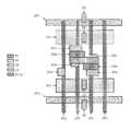
- FIG. 2schematically illustrates a cross-coupling-based design using diffusion contact structures, in accordance with an exemplary embodiment of the present disclosure.
- the design in FIG. 2includes gate structures (PC) 201 a , 201 b , 201 c , and 201 d over diffusion regions (RX) 203 having diffusion contact structures (CA) 205 , along with gate contacts (CB) 207 a through 207 g over gate structures 201 a through 201 d .
- PCgate structures
- 201 a , 201 b , 201 c , and 201 dover diffusion regions (RX) 203 having diffusion contact structures (CA) 205 , along with gate contacts (CB) 207 a through 207 g over gate structures 201 a through 201 d .
- CAdiffusion contact structures
- CBgate contacts
- PC cutgate cut region
- diffusion contact structure 211gate cut regions 209 a and 209 b , and gate contacts 207 a through 207 d that are within a two-gate pitch region (e.g., 2-CPP) enable four transistors (e.g., in a transmission gate) to be connected in the tightly dense two-gate pitch region.
- 2-CPPtwo-gate pitch region
- a transistor gate of the first transistormay correspond to a portion of gate structure 201 b overlapping with gate contact 207 a
- a transistor gate of the second transistormay correspond to a portion of gate structure 201 b overlapping with gate contact 207 b
- a transistor gate of the third transistormay correspond to a portion of gate structure 201 c overlapping with gate contact 207 c
- a transistor gate of the fourth transistormay correspond to a portion of gate structure 201 c overlapping with gate contact 207 d .
- FIGS. 3A through 3Cschematically illustrate various components of a cross-coupling-based multiplexer design using diffusion contact structures, in accordance with exemplary embodiments of the present disclosure.
- FIG. 3Aillustrates the multiplexer design with gate structures 301 over diffusion regions 303 , diffusion contact structures 305 over diffusion regions 303 , gate contacts 307 over gate structures 301 , via0 structures 309 to connect lower layer components to higher layer components (e.g., on different metal layers), and gate contacts 307 overlapping with top and bottom gate cut regions 311 that stretch across the top and bottom portions of gate structures 301 .
- the multiplexer designutilizes the cross-coupling-based design of FIG. 2 .
- the multiplexer designutilizes gate cut regions 311 to separate first and second gate contacts 307 over a first gate structure 301 from each other, and to separate third and fourth gate contacts 307 over a second gate structure 301 from each other.
- the multiplexer designutilizes diffusion contact structure 313 to couple one of those gate contacts 307 to another one of those gate contacts 307 (e.g., the second gate contact 307 to the third gate contact 307 ).
- the multiplexer design of FIGS. 3A through 3Cstretches across only 7-PC grids, as compared with the 9-PC grid requirement associated with a typical multiplexer design (e.g., the design of FIG. 1 ), resulting in a reduction of the cell area necessary for standard cells with multiplexer circuits.
- FIG. 3Bdepicts metal1 layer structures 315 and 317 (e.g., formed using different masks), metal2 layer structures 319 and 321 (e.g., formed using different masks), and via0 structures 309 that connect the lower layer components of FIG. 3A to the metal layers (via1 structures are not shown for illustrative convenience).
- FIG. 3Cillustrates the combination of the components of FIGS. 3A and 3B . As shown, the use of the cross-coupling-based design of FIG. 2 enables the multiplexer design to include four transistors to be connected in a tightly dense two-gate pitch region (e.g., at around the center of the multiplexer design).
- FIGS. 4A and 4Bschematically illustrate various components of a cross-coupling-based flip-flop design using diffusion contact structures, in accordance with exemplary embodiments of the present disclosure.
- FIG. 4Aillustrates the flip-flop design with various gate structures 401 , diffusion contact structures 403 , gate contacts 405 , via0 structures 407 , and gate cut regions 409 .
- the flop-flop designincludes three two-gate pitch regions, each of which may include four transistors based on the cross-coupling design of FIG. 2 .
- FIG. 4Bdepicts the flip-flop design with metal1 layer structures 413 as well metal2 layer structures 415 and 417 in addition to the components of FIG. 4A .
- typical flip-flop designsmay stretch over at least 24-PC grids.
- the flip-flop design of FIGS. 4A and 4B(based on the cross-coupling design of FIG. 2 ) stretches across only 21-PC grids, resulting in a reduction of the cell area necessary for standard cells with flip-flop circuits.
- the use of local gate contacts 405 (CB) and diffusion contact structures 403 (CA) as well as CA/CB handshakes, and the absence of various process complexities that burden typical cross-coupling-based designs, as illustrated in FIGS. 4A and 4Benable smaller cell size, lower costs, and improved reliability, as compared with standard cells based on typical cross-coupling-based designs.
- Embodiments of the present disclosurecan achieve several technical effects, including reduced cell size, lower costs, less complexity, and improved reliability.
- Embodiments of the present disclosureenjoy utility in various industrial applications as, for example, microprocessors, smart phones, mobile phones, cellular handsets, set-top boxes, DVD recorders and players, automotive navigation, printers and peripherals, networking and telecom equipment, gaming systems, and digital cameras.
- the present disclosuretherefore enjoys industrial applicability in any of various types of highly integrated semiconductor devices, particularly in 20 nm technology nodes and beyond.
Landscapes
- Engineering & Computer Science (AREA)
- Computer Hardware Design (AREA)
- Physics & Mathematics (AREA)
- General Physics & Mathematics (AREA)
- Theoretical Computer Science (AREA)
- Condensed Matter Physics & Semiconductors (AREA)
- Power Engineering (AREA)
- Microelectronics & Electronic Packaging (AREA)
- Manufacturing & Machinery (AREA)
- General Engineering & Computer Science (AREA)
- Geometry (AREA)
- Evolutionary Computation (AREA)
- Metal-Oxide And Bipolar Metal-Oxide Semiconductor Integrated Circuits (AREA)
- Design And Manufacture Of Integrated Circuits (AREA)
Abstract
Description
Claims (20)
Priority Applications (3)
| Application Number | Priority Date | Filing Date | Title |
|---|---|---|---|
| US13/561,932US8987128B2 (en) | 2012-07-30 | 2012-07-30 | Cross-coupling based design using diffusion contact structures |
| TW102102176ATWI528530B (en) | 2012-07-30 | 2013-01-21 | Cross-coupling based design using diffusion contact structures |
| CN201310042100.6ACN103579091B (en) | 2012-07-30 | 2013-02-01 | Use diffusion contact structure based on cross-linked design |
Applications Claiming Priority (1)
| Application Number | Priority Date | Filing Date | Title |
|---|---|---|---|
| US13/561,932US8987128B2 (en) | 2012-07-30 | 2012-07-30 | Cross-coupling based design using diffusion contact structures |
Publications (2)
| Publication Number | Publication Date |
|---|---|
| US20140027918A1 US20140027918A1 (en) | 2014-01-30 |
| US8987128B2true US8987128B2 (en) | 2015-03-24 |
Family
ID=49994095
Family Applications (1)
| Application Number | Title | Priority Date | Filing Date |
|---|---|---|---|
| US13/561,932Active2033-10-16US8987128B2 (en) | 2012-07-30 | 2012-07-30 | Cross-coupling based design using diffusion contact structures |
Country Status (3)
| Country | Link |
|---|---|
| US (1) | US8987128B2 (en) |
| CN (1) | CN103579091B (en) |
| TW (1) | TWI528530B (en) |
Cited By (12)
| Publication number | Priority date | Publication date | Assignee | Title |
|---|---|---|---|---|
| US9704862B2 (en) | 2014-09-18 | 2017-07-11 | Samsung Electronics Co., Ltd. | Semiconductor devices and methods for manufacturing the same |
| US9767248B2 (en) | 2014-09-18 | 2017-09-19 | Samsung Electronics, Co., Ltd. | Semiconductor having cross coupled structure and layout verification method thereof |
| US9811626B2 (en) | 2014-09-18 | 2017-11-07 | Samsung Electronics Co., Ltd. | Method of designing layout of semiconductor device |
| US20170337320A1 (en)* | 2016-05-18 | 2017-11-23 | Matthew Berzins | Using deep sub-micron stress effects and proximity effects to create a high performance standard cell |
| US10026661B2 (en) | 2014-09-18 | 2018-07-17 | Samsung Electronics Co., Ltd. | Semiconductor device for testing large number of devices and composing method and test method thereof |
| US10095825B2 (en) | 2014-09-18 | 2018-10-09 | Samsung Electronics Co., Ltd. | Computer based system for verifying layout of semiconductor device and layout verify method thereof |
| US10249605B2 (en) | 2016-12-07 | 2019-04-02 | Samsung Electronics Co., Ltd. | Integrated circuit devices |
| US10504894B2 (en) | 2015-12-07 | 2019-12-10 | Samsung Electronics Co., Ltd. | Semiconductor device |
| US10515943B2 (en) | 2016-10-17 | 2019-12-24 | Samsung Electronics Co., Ltd. | Integrated circuit and semiconductor device |
| US10692808B2 (en) | 2017-09-18 | 2020-06-23 | Qualcomm Incorporated | High performance cell design in a technology with high density metal routing |
| US10943923B2 (en) | 2019-04-02 | 2021-03-09 | Samsung Electronics Co., Ltd. | Integrated circuits and semiconductor device including standard cell |
| US20210183859A1 (en)* | 2019-12-17 | 2021-06-17 | Samsung Electronics Co., Ltd. | Semiconductor integrated circuit |
Families Citing this family (13)
| Publication number | Priority date | Publication date | Assignee | Title |
|---|---|---|---|---|
| KR102423878B1 (en)* | 2014-09-18 | 2022-07-22 | 삼성전자주식회사 | Semiconductor device for testing a large number of devices and composing method and test method thereof |
| US9589955B2 (en) | 2014-10-01 | 2017-03-07 | Samsung Electronics Co., Ltd. | System on chip |
| KR102288869B1 (en) | 2014-10-01 | 2021-08-10 | 삼성전자주식회사 | System on chip |
| KR102368072B1 (en)* | 2014-10-02 | 2022-02-28 | 삼성전자주식회사 | Scan flop flop and Scan test circuit including the scan flip flip |
| US9753086B2 (en) | 2014-10-02 | 2017-09-05 | Samsung Electronics Co., Ltd. | Scan flip-flop and scan test circuit including the same |
| KR102254031B1 (en) | 2014-10-10 | 2021-05-20 | 삼성전자주식회사 | Semiconductor device and Method of manufacturing the same |
| US9431300B1 (en)* | 2015-08-27 | 2016-08-30 | Globalfoundries Inc. | MOL architecture enabling ultra-regular cross couple |
| US10163879B2 (en) | 2015-10-05 | 2018-12-25 | Samsung Electronics Co., Ltd. | Semiconductor device having jumper pattern |
| US10262941B2 (en)* | 2016-04-22 | 2019-04-16 | Globalfoundries Inc. | Devices and methods for forming cross coupled contacts |
| KR102699046B1 (en) | 2016-12-15 | 2024-08-27 | 삼성전자주식회사 | Integrated circuit having vertical transistor and semiconductor device including the same |
| WO2020170715A1 (en)* | 2019-02-18 | 2020-08-27 | 株式会社ソシオネクスト | Semiconductor integrated circuit device |
| KR20220128040A (en)* | 2021-03-12 | 2022-09-20 | 삼성전자주식회사 | semiconductor device |
| CN116247050A (en)* | 2022-01-30 | 2023-06-09 | 台湾积体电路制造股份有限公司 | Current Distribution Pin Structure and Forming Method |
Citations (2)
| Publication number | Priority date | Publication date | Assignee | Title |
|---|---|---|---|---|
| US8679911B2 (en)* | 2012-05-07 | 2014-03-25 | Globalfoundries Inc. | Cross-coupling-based design using diffusion contact structures |
| US8741763B2 (en)* | 2012-05-07 | 2014-06-03 | Globalfoundries Inc. | Layout designs with via routing structures |
Family Cites Families (3)
| Publication number | Priority date | Publication date | Assignee | Title |
|---|---|---|---|---|
| KR100436673B1 (en)* | 2001-05-28 | 2004-07-02 | 가부시끼가이샤 도시바 | Semiconductor device and manufacturing method thereof |
| US7446352B2 (en)* | 2006-03-09 | 2008-11-04 | Tela Innovations, Inc. | Dynamic array architecture |
| US8258578B2 (en)* | 2009-08-31 | 2012-09-04 | Advanced Micro Devices, Inc. | Handshake structure for improving layout density |
- 2012
- 2012-07-30USUS13/561,932patent/US8987128B2/enactiveActive
- 2013
- 2013-01-21TWTW102102176Apatent/TWI528530B/enactive
- 2013-02-01CNCN201310042100.6Apatent/CN103579091B/enactiveActive
Patent Citations (3)
| Publication number | Priority date | Publication date | Assignee | Title |
|---|---|---|---|---|
| US8679911B2 (en)* | 2012-05-07 | 2014-03-25 | Globalfoundries Inc. | Cross-coupling-based design using diffusion contact structures |
| US20140131816A1 (en)* | 2012-05-07 | 2014-05-15 | GLOBALFOUNDERS Inc. | Cross-coupling-based design using diffusion contact structures |
| US8741763B2 (en)* | 2012-05-07 | 2014-06-03 | Globalfoundries Inc. | Layout designs with via routing structures |
Cited By (21)
| Publication number | Priority date | Publication date | Assignee | Title |
|---|---|---|---|---|
| US10095825B2 (en) | 2014-09-18 | 2018-10-09 | Samsung Electronics Co., Ltd. | Computer based system for verifying layout of semiconductor device and layout verify method thereof |
| US9767248B2 (en) | 2014-09-18 | 2017-09-19 | Samsung Electronics, Co., Ltd. | Semiconductor having cross coupled structure and layout verification method thereof |
| US9811626B2 (en) | 2014-09-18 | 2017-11-07 | Samsung Electronics Co., Ltd. | Method of designing layout of semiconductor device |
| US9704862B2 (en) | 2014-09-18 | 2017-07-11 | Samsung Electronics Co., Ltd. | Semiconductor devices and methods for manufacturing the same |
| US10242984B2 (en) | 2014-09-18 | 2019-03-26 | Samsung Electronics Co., Ltd. | Semiconductor devices and methods for manufacturing the same |
| US10002223B2 (en) | 2014-09-18 | 2018-06-19 | Samsung Electronics Co., Ltd. | Method of designing layout of semiconductor device |
| US10026661B2 (en) | 2014-09-18 | 2018-07-17 | Samsung Electronics Co., Ltd. | Semiconductor device for testing large number of devices and composing method and test method thereof |
| US10504894B2 (en) | 2015-12-07 | 2019-12-10 | Samsung Electronics Co., Ltd. | Semiconductor device |
| US10714473B2 (en) | 2015-12-07 | 2020-07-14 | Samsung Electronics Co., Ltd. | Semiconductor device |
| US11581311B2 (en) | 2015-12-07 | 2023-02-14 | Samsung Electronics Co., Ltd. | Semiconductor device |
| US10950604B2 (en) | 2015-12-07 | 2021-03-16 | Samsung Electronics Co., Ltd. | Semiconductor device |
| US20170337320A1 (en)* | 2016-05-18 | 2017-11-23 | Matthew Berzins | Using deep sub-micron stress effects and proximity effects to create a high performance standard cell |
| US9904758B2 (en)* | 2016-05-18 | 2018-02-27 | Samsung Electronics Co., Ltd. | Using deep sub-micron stress effects and proximity effects to create a high performance standard cell |
| US10804257B2 (en) | 2016-10-17 | 2020-10-13 | Samsung Electronics Co., Ltd. | Integrated circuit and semiconductor device |
| US10515943B2 (en) | 2016-10-17 | 2019-12-24 | Samsung Electronics Co., Ltd. | Integrated circuit and semiconductor device |
| US11289469B2 (en) | 2016-10-17 | 2022-03-29 | Samsung Electronics Co., Ltd. | Integrated circuit and semiconductor device |
| US10249605B2 (en) | 2016-12-07 | 2019-04-02 | Samsung Electronics Co., Ltd. | Integrated circuit devices |
| US10692808B2 (en) | 2017-09-18 | 2020-06-23 | Qualcomm Incorporated | High performance cell design in a technology with high density metal routing |
| US10943923B2 (en) | 2019-04-02 | 2021-03-09 | Samsung Electronics Co., Ltd. | Integrated circuits and semiconductor device including standard cell |
| US20210183859A1 (en)* | 2019-12-17 | 2021-06-17 | Samsung Electronics Co., Ltd. | Semiconductor integrated circuit |
| US11631672B2 (en)* | 2019-12-17 | 2023-04-18 | Samsung Electronics Co., Ltd. | Semiconductor integrated circuit |
Also Published As
| Publication number | Publication date |
|---|---|
| US20140027918A1 (en) | 2014-01-30 |
| TW201405776A (en) | 2014-02-01 |
| TWI528530B (en) | 2016-04-01 |
| CN103579091A (en) | 2014-02-12 |
| CN103579091B (en) | 2016-12-28 |
Similar Documents
| Publication | Publication Date | Title |
|---|---|---|
| US8987128B2 (en) | Cross-coupling based design using diffusion contact structures | |
| US8741763B2 (en) | Layout designs with via routing structures | |
| US9159724B2 (en) | Cross-coupling-based design using diffusion contact structures | |
| US9634003B2 (en) | Special construct for continuous non-uniform RX FinFET standard cells | |
| US9437588B1 (en) | Middle of-line architecture for dense library layout using M0 hand-shake | |
| US8987816B2 (en) | Contact power rail | |
| US10103066B2 (en) | Method of utilizing trench silicide in a gate cross-couple construct | |
| US9006100B2 (en) | Middle-of-the-line constructs using diffusion contact structures | |
| US9431300B1 (en) | MOL architecture enabling ultra-regular cross couple | |
| US9406775B1 (en) | Method for creating self-aligned compact contacts in an IC device meeting fabrication spacing constraints | |
| US9406616B2 (en) | Merged source/drain and gate contacts in SRAM bitcell | |
| US9105643B2 (en) | Bit cell with double patterned metal layer structures | |
| US9147028B2 (en) | Forming modified cell architecture for finFET technology and resulting device | |
| US20150311122A1 (en) | Forming gate tie between abutting cells and resulting device | |
| KR20150121907A (en) | Semiconductor device and method for fabricating the same | |
| US10283505B2 (en) | Dummy gate used as interconnection and method of making the same | |
| US20160141291A1 (en) | Metal segments as landing pads and local interconnects in an ic device | |
| US8791577B2 (en) | Bit cell with triple patterned metal layer structures | |
| TWI528528B (en) | Integrated circuit configuration and fabricating method thereof | |
| TWM623394U (en) | Semiconductor structure and associated chip and electronic device |
Legal Events
| Date | Code | Title | Description |
|---|---|---|---|
| AS | Assignment | Owner name:GLOBALFOUNDRIES INC., CAYMAN ISLANDS Free format text:ASSIGNMENT OF ASSIGNORS INTEREST;ASSIGNORS:RASHED, MAHBUB;TARABBIA, MARC;NGUYEN, CHINH;AND OTHERS;SIGNING DATES FROM 20120723 TO 20120730;REEL/FRAME:028686/0759 | |
| FEPP | Fee payment procedure | Free format text:PAYOR NUMBER ASSIGNED (ORIGINAL EVENT CODE: ASPN); ENTITY STATUS OF PATENT OWNER: LARGE ENTITY | |
| STCF | Information on status: patent grant | Free format text:PATENTED CASE | |
| FEPP | Fee payment procedure | Free format text:MAINTENANCE FEE REMINDER MAILED (ORIGINAL EVENT CODE: REM.); ENTITY STATUS OF PATENT OWNER: LARGE ENTITY | |
| AS | Assignment | Owner name:WILMINGTON TRUST, NATIONAL ASSOCIATION, DELAWARE Free format text:SECURITY AGREEMENT;ASSIGNOR:GLOBALFOUNDRIES INC.;REEL/FRAME:049490/0001 Effective date:20181127 | |
| FEPP | Fee payment procedure | Free format text:SURCHARGE FOR LATE PAYMENT, LARGE ENTITY (ORIGINAL EVENT CODE: M1554); ENTITY STATUS OF PATENT OWNER: LARGE ENTITY | |
| MAFP | Maintenance fee payment | Free format text:PAYMENT OF MAINTENANCE FEE, 4TH YEAR, LARGE ENTITY (ORIGINAL EVENT CODE: M1551); ENTITY STATUS OF PATENT OWNER: LARGE ENTITY Year of fee payment:4 | |
| AS | Assignment | Owner name:GLOBALFOUNDRIES INC., CAYMAN ISLANDS Free format text:RELEASE BY SECURED PARTY;ASSIGNOR:WILMINGTON TRUST, NATIONAL ASSOCIATION;REEL/FRAME:054636/0001 Effective date:20201117 | |
| AS | Assignment | Owner name:GLOBALFOUNDRIES U.S. INC., NEW YORK Free format text:RELEASE BY SECURED PARTY;ASSIGNOR:WILMINGTON TRUST, NATIONAL ASSOCIATION;REEL/FRAME:056987/0001 Effective date:20201117 | |
| MAFP | Maintenance fee payment | Free format text:PAYMENT OF MAINTENANCE FEE, 8TH YEAR, LARGE ENTITY (ORIGINAL EVENT CODE: M1552); ENTITY STATUS OF PATENT OWNER: LARGE ENTITY Year of fee payment:8 |