US8987069B1 - Semiconductor substrate with multiple SiGe regions having different germanium concentrations by a single epitaxy process - Google Patents
Semiconductor substrate with multiple SiGe regions having different germanium concentrations by a single epitaxy processDownload PDFInfo
- Publication number
- US8987069B1 US8987069B1US14/096,120US201314096120AUS8987069B1US 8987069 B1US8987069 B1US 8987069B1US 201314096120 AUS201314096120 AUS 201314096120AUS 8987069 B1US8987069 B1US 8987069B1
- Authority
- US
- United States
- Prior art keywords
- sige layer
- layer
- sige
- germanium
- active regions
- Prior art date
- Legal status (The legal status is an assumption and is not a legal conclusion. Google has not performed a legal analysis and makes no representation as to the accuracy of the status listed.)
- Active
Links
- 229910000577Silicon-germaniumInorganic materials0.000titleclaimsabstractdescription183
- 229910052732germaniumInorganic materials0.000titleclaimsabstractdescription88
- GNPVGFCGXDBREM-UHFFFAOYSA-Ngermanium atomChemical compound[Ge]GNPVGFCGXDBREM-UHFFFAOYSA-N0.000titleclaimsabstractdescription85
- 239000000758substrateSubstances0.000titleclaimsabstractdescription70
- 238000000034methodMethods0.000titleclaimsabstractdescription56
- 239000004065semiconductorSubstances0.000titleclaimsdescription86
- 238000000407epitaxyMethods0.000titledescription3
- 238000000151depositionMethods0.000claimsabstractdescription32
- 238000002156mixingMethods0.000claimsabstractdescription13
- 239000000463materialSubstances0.000claimsdescription65
- 239000012212insulatorSubstances0.000claimsdescription18
- 230000008021depositionEffects0.000claimsdescription16
- 239000000203mixtureSubstances0.000claimsdescription3
- 229910052710siliconInorganic materials0.000abstractdescription34
- XUIMIQQOPSSXEZ-UHFFFAOYSA-NSiliconChemical compound[Si]XUIMIQQOPSSXEZ-UHFFFAOYSA-N0.000abstractdescription33
- 239000010703siliconSubstances0.000abstractdescription33
- 238000002955isolationMethods0.000description16
- VYPSYNLAJGMNEJ-UHFFFAOYSA-NSilicium dioxideChemical compoundO=[Si]=OVYPSYNLAJGMNEJ-UHFFFAOYSA-N0.000description9
- LEVVHYCKPQWKOP-UHFFFAOYSA-N[Si].[Ge]Chemical compound[Si].[Ge]LEVVHYCKPQWKOP-UHFFFAOYSA-N0.000description8
- 239000007789gasSubstances0.000description8
- 239000013078crystalSubstances0.000description6
- -1nFETs and pFETS)Substances0.000description5
- 238000000137annealingMethods0.000description4
- 235000012239silicon dioxideNutrition0.000description4
- 239000000377silicon dioxideSubstances0.000description4
- 229910052581Si3N4Inorganic materials0.000description3
- 230000008901benefitEffects0.000description3
- 238000005137deposition processMethods0.000description3
- 229910044991metal oxideInorganic materials0.000description3
- 150000004706metal oxidesChemical class0.000description3
- 150000004767nitridesChemical class0.000description3
- 230000003647oxidationEffects0.000description3
- 238000007254oxidation reactionMethods0.000description3
- HQVNEWCFYHHQES-UHFFFAOYSA-Nsilicon nitrideChemical compoundN12[Si]34N5[Si]62N3[Si]51N64HQVNEWCFYHHQES-UHFFFAOYSA-N0.000description3
- XKRFYHLGVUSROY-UHFFFAOYSA-NArgonChemical compound[Ar]XKRFYHLGVUSROY-UHFFFAOYSA-N0.000description2
- IJGRMHOSHXDMSA-UHFFFAOYSA-NAtomic nitrogenChemical compoundN#NIJGRMHOSHXDMSA-UHFFFAOYSA-N0.000description2
- 208000012868OvergrowthDiseases0.000description2
- 238000001505atmospheric-pressure chemical vapour depositionMethods0.000description2
- 125000004429atomChemical group0.000description2
- 230000007547defectEffects0.000description2
- 239000003989dielectric materialSubstances0.000description2
- 238000010790dilutionMethods0.000description2
- 239000012895dilutionSubstances0.000description2
- 238000005530etchingMethods0.000description2
- 239000012467final productSubstances0.000description2
- 238000005468ion implantationMethods0.000description2
- 238000001289rapid thermal chemical vapour depositionMethods0.000description2
- WGTYBPLFGIVFAS-UHFFFAOYSA-Mtetramethylammonium hydroxideChemical compound[OH-].C[N+](C)(C)CWGTYBPLFGIVFAS-UHFFFAOYSA-M0.000description2
- 238000000038ultrahigh vacuum chemical vapour depositionMethods0.000description2
- 229910001218Gallium arsenideInorganic materials0.000description1
- 229910000673Indium arsenideInorganic materials0.000description1
- 229910003811SiGeCInorganic materials0.000description1
- BLRPTPMANUNPDV-UHFFFAOYSA-NSilaneChemical compound[SiH4]BLRPTPMANUNPDV-UHFFFAOYSA-N0.000description1
- 229910045601alloyInorganic materials0.000description1
- 239000000956alloySubstances0.000description1
- 229910052786argonInorganic materials0.000description1
- 230000015572biosynthetic processEffects0.000description1
- 239000012159carrier gasSubstances0.000description1
- 238000005229chemical vapour depositionMethods0.000description1
- 230000000295complement effectEffects0.000description1
- 150000001875compoundsChemical class0.000description1
- 239000004020conductorSubstances0.000description1
- 238000005336crackingMethods0.000description1
- 238000000280densificationMethods0.000description1
- OXTURSYJKMYFLT-UHFFFAOYSA-NdichlorogermaneChemical compoundCl[GeH2]ClOXTURSYJKMYFLT-UHFFFAOYSA-N0.000description1
- MROCJMGDEKINLD-UHFFFAOYSA-NdichlorosilaneChemical compoundCl[SiH2]ClMROCJMGDEKINLD-UHFFFAOYSA-N0.000description1
- 238000009792diffusion processMethods0.000description1
- VXGHASBVNMHGDI-UHFFFAOYSA-NdigermaneChemical compound[Ge][Ge]VXGHASBVNMHGDI-UHFFFAOYSA-N0.000description1
- UCMVNBCLTOOHMN-UHFFFAOYSA-Ndimethyl(silyl)silaneChemical compoundC[SiH](C)[SiH3]UCMVNBCLTOOHMN-UHFFFAOYSA-N0.000description1
- UBHZUDXTHNMNLD-UHFFFAOYSA-NdimethylsilaneChemical compoundC[SiH2]CUBHZUDXTHNMNLD-UHFFFAOYSA-N0.000description1
- PZPGRFITIJYNEJ-UHFFFAOYSA-NdisilaneChemical compound[SiH3][SiH3]PZPGRFITIJYNEJ-UHFFFAOYSA-N0.000description1
- 239000002019doping agentSubstances0.000description1
- 230000000694effectsEffects0.000description1
- KCWYOFZQRFCIIE-UHFFFAOYSA-NethylsilaneChemical compoundCC[SiH3]KCWYOFZQRFCIIE-UHFFFAOYSA-N0.000description1
- 230000005669field effectEffects0.000description1
- 238000011049fillingMethods0.000description1
- 229910000078germaneInorganic materials0.000description1
- 239000001307heliumSubstances0.000description1
- 229910052734heliumInorganic materials0.000description1
- SWQJXJOGLNCZEY-UHFFFAOYSA-Nhelium atomChemical compound[He]SWQJXJOGLNCZEY-UHFFFAOYSA-N0.000description1
- NEXSMEBSBIABKL-UHFFFAOYSA-NhexamethyldisilaneChemical compoundC[Si](C)(C)[Si](C)(C)CNEXSMEBSBIABKL-UHFFFAOYSA-N0.000description1
- 239000001257hydrogenSubstances0.000description1
- 229910052739hydrogenInorganic materials0.000description1
- 125000004435hydrogen atomChemical class[H]*0.000description1
- RPQDHPTXJYYUPQ-UHFFFAOYSA-Nindium arsenideChemical compound[In]#[As]RPQDHPTXJYYUPQ-UHFFFAOYSA-N0.000description1
- 239000011810insulating materialSubstances0.000description1
- 238000001459lithographyMethods0.000description1
- 230000000873masking effectEffects0.000description1
- IQCYANORSDPPDT-UHFFFAOYSA-Nmethyl(silyl)silaneChemical compoundC[SiH2][SiH3]IQCYANORSDPPDT-UHFFFAOYSA-N0.000description1
- UIUXUFNYAYAMOE-UHFFFAOYSA-NmethylsilaneChemical compound[SiH3]CUIUXUFNYAYAMOE-UHFFFAOYSA-N0.000description1
- 229910003465moissaniteInorganic materials0.000description1
- 238000001451molecular beam epitaxyMethods0.000description1
- 229910052757nitrogenInorganic materials0.000description1
- 230000000704physical effectEffects0.000description1
- 238000005240physical vapour depositionMethods0.000description1
- 239000000376reactantSubstances0.000description1
- 229910000077silaneInorganic materials0.000description1
- 229910010271silicon carbideInorganic materials0.000description1
- 229910052814silicon oxideInorganic materials0.000description1
- FDNAPBUWERUEDA-UHFFFAOYSA-Nsilicon tetrachlorideChemical compoundCl[Si](Cl)(Cl)ClFDNAPBUWERUEDA-UHFFFAOYSA-N0.000description1
- 239000000126substanceSubstances0.000description1
- 230000002459sustained effectEffects0.000description1
- IEXRMSFAVATTJX-UHFFFAOYSA-NtetrachlorogermaneChemical compoundCl[Ge](Cl)(Cl)ClIEXRMSFAVATTJX-UHFFFAOYSA-N0.000description1
- LXEXBJXDGVGRAR-UHFFFAOYSA-Ntrichloro(trichlorosilyl)silaneChemical compoundCl[Si](Cl)(Cl)[Si](Cl)(Cl)ClLXEXBJXDGVGRAR-UHFFFAOYSA-N0.000description1
- MUDDKLJPADVVKF-UHFFFAOYSA-NtrichlorogermaneChemical compoundCl[GeH](Cl)ClMUDDKLJPADVVKF-UHFFFAOYSA-N0.000description1
- ZDHXKXAHOVTTAH-UHFFFAOYSA-NtrichlorosilaneChemical compoundCl[SiH](Cl)ClZDHXKXAHOVTTAH-UHFFFAOYSA-N0.000description1
- 239000005052trichlorosilaneSubstances0.000description1
- VEDJZFSRVVQBIL-UHFFFAOYSA-NtrisilaneChemical compound[SiH3][SiH2][SiH3]VEDJZFSRVVQBIL-UHFFFAOYSA-N0.000description1
- 238000009279wet oxidation reactionMethods0.000description1
Images


Classifications
- H—ELECTRICITY
- H10—SEMICONDUCTOR DEVICES; ELECTRIC SOLID-STATE DEVICES NOT OTHERWISE PROVIDED FOR
- H10D—INORGANIC ELECTRIC SEMICONDUCTOR DEVICES
- H10D86/00—Integrated devices formed in or on insulating or conducting substrates, e.g. formed in silicon-on-insulator [SOI] substrates or on stainless steel or glass substrates
- H10D86/201—Integrated devices formed in or on insulating or conducting substrates, e.g. formed in silicon-on-insulator [SOI] substrates or on stainless steel or glass substrates the substrates comprising an insulating layer on a semiconductor body, e.g. SOI
- H01L29/161—
- H—ELECTRICITY
- H01—ELECTRIC ELEMENTS
- H01L—SEMICONDUCTOR DEVICES NOT COVERED BY CLASS H10
- H01L21/00—Processes or apparatus adapted for the manufacture or treatment of semiconductor or solid state devices or of parts thereof
- H01L21/02—Manufacture or treatment of semiconductor devices or of parts thereof
- H01L21/02104—Forming layers
- H01L21/02365—Forming inorganic semiconducting materials on a substrate
- H01L21/02436—Intermediate layers between substrates and deposited layers
- H01L21/02439—Materials
- H01L21/02441—Group 14 semiconducting materials
- H01L21/0245—Silicon, silicon germanium, germanium
- H—ELECTRICITY
- H01—ELECTRIC ELEMENTS
- H01L—SEMICONDUCTOR DEVICES NOT COVERED BY CLASS H10
- H01L21/00—Processes or apparatus adapted for the manufacture or treatment of semiconductor or solid state devices or of parts thereof
- H01L21/02—Manufacture or treatment of semiconductor devices or of parts thereof
- H01L21/02104—Forming layers
- H01L21/02365—Forming inorganic semiconducting materials on a substrate
- H01L21/02436—Intermediate layers between substrates and deposited layers
- H01L21/02494—Structure
- H—ELECTRICITY
- H01—ELECTRIC ELEMENTS
- H01L—SEMICONDUCTOR DEVICES NOT COVERED BY CLASS H10
- H01L21/00—Processes or apparatus adapted for the manufacture or treatment of semiconductor or solid state devices or of parts thereof
- H01L21/02—Manufacture or treatment of semiconductor devices or of parts thereof
- H01L21/02104—Forming layers
- H01L21/02365—Forming inorganic semiconducting materials on a substrate
- H01L21/02436—Intermediate layers between substrates and deposited layers
- H01L21/02516—Crystal orientation
- H—ELECTRICITY
- H01—ELECTRIC ELEMENTS
- H01L—SEMICONDUCTOR DEVICES NOT COVERED BY CLASS H10
- H01L21/00—Processes or apparatus adapted for the manufacture or treatment of semiconductor or solid state devices or of parts thereof
- H01L21/02—Manufacture or treatment of semiconductor devices or of parts thereof
- H01L21/02104—Forming layers
- H01L21/02365—Forming inorganic semiconducting materials on a substrate
- H01L21/02518—Deposited layers
- H01L21/02521—Materials
- H01L21/02524—Group 14 semiconducting materials
- H01L21/02532—Silicon, silicon germanium, germanium
- H—ELECTRICITY
- H01—ELECTRIC ELEMENTS
- H01L—SEMICONDUCTOR DEVICES NOT COVERED BY CLASS H10
- H01L21/00—Processes or apparatus adapted for the manufacture or treatment of semiconductor or solid state devices or of parts thereof
- H01L21/02—Manufacture or treatment of semiconductor devices or of parts thereof
- H01L21/02104—Forming layers
- H01L21/02365—Forming inorganic semiconducting materials on a substrate
- H01L21/02612—Formation types
- H01L21/02617—Deposition types
- H01L21/0262—Reduction or decomposition of gaseous compounds, e.g. CVD
- H—ELECTRICITY
- H01—ELECTRIC ELEMENTS
- H01L—SEMICONDUCTOR DEVICES NOT COVERED BY CLASS H10
- H01L21/00—Processes or apparatus adapted for the manufacture or treatment of semiconductor or solid state devices or of parts thereof
- H01L21/02—Manufacture or treatment of semiconductor devices or of parts thereof
- H01L21/02104—Forming layers
- H01L21/02365—Forming inorganic semiconducting materials on a substrate
- H01L21/02656—Special treatments
- H01L21/02664—Aftertreatments
- H—ELECTRICITY
- H01—ELECTRIC ELEMENTS
- H01L—SEMICONDUCTOR DEVICES NOT COVERED BY CLASS H10
- H01L21/00—Processes or apparatus adapted for the manufacture or treatment of semiconductor or solid state devices or of parts thereof
- H01L21/02—Manufacture or treatment of semiconductor devices or of parts thereof
- H01L21/04—Manufacture or treatment of semiconductor devices or of parts thereof the devices having potential barriers, e.g. a PN junction, depletion layer or carrier concentration layer
- H01L21/18—Manufacture or treatment of semiconductor devices or of parts thereof the devices having potential barriers, e.g. a PN junction, depletion layer or carrier concentration layer the devices having semiconductor bodies comprising elements of Group IV of the Periodic Table or AIIIBV compounds with or without impurities, e.g. doping materials
- H01L21/22—Diffusion of impurity materials, e.g. doping materials, electrode materials, into or out of a semiconductor body, or between semiconductor regions; Interactions between two or more impurities; Redistribution of impurities
- H01L21/225—Diffusion of impurity materials, e.g. doping materials, electrode materials, into or out of a semiconductor body, or between semiconductor regions; Interactions between two or more impurities; Redistribution of impurities using diffusion into or out of a solid from or into a solid phase, e.g. a doped oxide layer
- H01L21/2251—Diffusion into or out of group IV semiconductors
- H01L27/088—
- H01L29/0649—
- H01L29/1033—
- H—ELECTRICITY
- H10—SEMICONDUCTOR DEVICES; ELECTRIC SOLID-STATE DEVICES NOT OTHERWISE PROVIDED FOR
- H10D—INORGANIC ELECTRIC SEMICONDUCTOR DEVICES
- H10D62/00—Semiconductor bodies, or regions thereof, of devices having potential barriers
- H10D62/10—Shapes, relative sizes or dispositions of the regions of the semiconductor bodies; Shapes of the semiconductor bodies
- H10D62/113—Isolations within a component, i.e. internal isolations
- H10D62/115—Dielectric isolations, e.g. air gaps
- H—ELECTRICITY
- H10—SEMICONDUCTOR DEVICES; ELECTRIC SOLID-STATE DEVICES NOT OTHERWISE PROVIDED FOR
- H10D—INORGANIC ELECTRIC SEMICONDUCTOR DEVICES
- H10D62/00—Semiconductor bodies, or regions thereof, of devices having potential barriers
- H10D62/10—Shapes, relative sizes or dispositions of the regions of the semiconductor bodies; Shapes of the semiconductor bodies
- H10D62/17—Semiconductor regions connected to electrodes not carrying current to be rectified, amplified or switched, e.g. channel regions
- H10D62/213—Channel regions of field-effect devices
- H10D62/221—Channel regions of field-effect devices of FETs
- H10D62/235—Channel regions of field-effect devices of FETs of IGFETs
- H—ELECTRICITY
- H10—SEMICONDUCTOR DEVICES; ELECTRIC SOLID-STATE DEVICES NOT OTHERWISE PROVIDED FOR
- H10D—INORGANIC ELECTRIC SEMICONDUCTOR DEVICES
- H10D62/00—Semiconductor bodies, or regions thereof, of devices having potential barriers
- H10D62/80—Semiconductor bodies, or regions thereof, of devices having potential barriers characterised by the materials
- H10D62/83—Semiconductor bodies, or regions thereof, of devices having potential barriers characterised by the materials being Group IV materials, e.g. B-doped Si or undoped Ge
- H10D62/832—Semiconductor bodies, or regions thereof, of devices having potential barriers characterised by the materials being Group IV materials, e.g. B-doped Si or undoped Ge being Group IV materials comprising two or more elements, e.g. SiGe
- H—ELECTRICITY
- H10—SEMICONDUCTOR DEVICES; ELECTRIC SOLID-STATE DEVICES NOT OTHERWISE PROVIDED FOR
- H10D—INORGANIC ELECTRIC SEMICONDUCTOR DEVICES
- H10D86/00—Integrated devices formed in or on insulating or conducting substrates, e.g. formed in silicon-on-insulator [SOI] substrates or on stainless steel or glass substrates
- H10D86/01—Manufacture or treatment
- H—ELECTRICITY
- H10—SEMICONDUCTOR DEVICES; ELECTRIC SOLID-STATE DEVICES NOT OTHERWISE PROVIDED FOR
- H10D—INORGANIC ELECTRIC SEMICONDUCTOR DEVICES
- H10D84/00—Integrated devices formed in or on semiconductor substrates that comprise only semiconducting layers, e.g. on Si wafers or on GaAs-on-Si wafers
- H10D84/01—Manufacture or treatment
- H10D84/0123—Integrating together multiple components covered by H10D12/00 or H10D30/00, e.g. integrating multiple IGBTs
- H10D84/0126—Integrating together multiple components covered by H10D12/00 or H10D30/00, e.g. integrating multiple IGBTs the components including insulated gates, e.g. IGFETs
- H10D84/0128—Manufacturing their channels
- H—ELECTRICITY
- H10—SEMICONDUCTOR DEVICES; ELECTRIC SOLID-STATE DEVICES NOT OTHERWISE PROVIDED FOR
- H10D—INORGANIC ELECTRIC SEMICONDUCTOR DEVICES
- H10D84/00—Integrated devices formed in or on semiconductor substrates that comprise only semiconducting layers, e.g. on Si wafers or on GaAs-on-Si wafers
- H10D84/01—Manufacture or treatment
- H10D84/02—Manufacture or treatment characterised by using material-based technologies
- H10D84/03—Manufacture or treatment characterised by using material-based technologies using Group IV technology, e.g. silicon technology or silicon-carbide [SiC] technology
- H10D84/038—Manufacture or treatment characterised by using material-based technologies using Group IV technology, e.g. silicon technology or silicon-carbide [SiC] technology using silicon technology, e.g. SiGe
- H—ELECTRICITY
- H10—SEMICONDUCTOR DEVICES; ELECTRIC SOLID-STATE DEVICES NOT OTHERWISE PROVIDED FOR
- H10D—INORGANIC ELECTRIC SEMICONDUCTOR DEVICES
- H10D84/00—Integrated devices formed in or on semiconductor substrates that comprise only semiconducting layers, e.g. on Si wafers or on GaAs-on-Si wafers
- H10D84/80—Integrated devices formed in or on semiconductor substrates that comprise only semiconducting layers, e.g. on Si wafers or on GaAs-on-Si wafers characterised by the integration of at least one component covered by groups H10D12/00 or H10D30/00, e.g. integration of IGFETs
- H10D84/82—Integrated devices formed in or on semiconductor substrates that comprise only semiconducting layers, e.g. on Si wafers or on GaAs-on-Si wafers characterised by the integration of at least one component covered by groups H10D12/00 or H10D30/00, e.g. integration of IGFETs of only field-effect components
- H10D84/83—Integrated devices formed in or on semiconductor substrates that comprise only semiconducting layers, e.g. on Si wafers or on GaAs-on-Si wafers characterised by the integration of at least one component covered by groups H10D12/00 or H10D30/00, e.g. integration of IGFETs of only field-effect components of only insulated-gate FETs [IGFET]
Definitions
- the present inventionrelates to semiconductor structure and semiconductor devices containing germanium, and more particularly, to semiconductor structures and semiconductor devices containing silicon germanium layers.
- MOSFETsmetal oxide semiconductor field effect transistors
- CMOScomplementary metal oxide semiconductor
- One aspect of the Inventionis directed to improve device performance and to have different threshold voltages. For example, it may be desirable to use different SiGe channel materials for the different pFETs in a circuit (or nFETs and other devices.); and while it may be desirable to fabricate pFETs with a SiGe channel having, for example, 25% Germanium, it may be desirable to fabricate another set of pFETs with a SiGe channel having, for example, 40% Germanium. Further, different sets of pFETs are often fabricated on the same substrate. Therefore, it may be desirable to form regions of two different pFET, (or another kind of device, i.e. nFET, and/or different sets of devices on the same substrate, i.e. nFETs and pFETS), semiconductor materials on the same substrate.
- One aspect of the inventionincludes a method for preparing a semiconductor substrate with multiple Silicon-Germanium (SiGe) regions having different Germanium concentrations by a single epitaxy process.
- the methodincludes: providing an ETSOI substrate with at least two active regions, depositing a first SiGe layer over each of the at least two active regions, depositing a Silicon layer over each of the SiGe layers, depositing a second SiGe layer over each of the Silicon layers, depositing a hard mask over one of the at least two active regions, removing the deposited second SiGe layer of an unmasked active region of the at least two active regions, removing the deposited hard mask over the second SiGe layer of one of the at least two active regions, and thermally mixing the remaining Si and SiGe layers of the at least two active regions to form a new SiGe layer with uniform Germanium concentration for each of the at least two active regions, where the new SiGe layer with uniform Germanium concentration of one of the at least two active regions has a different concentration of Germanium than the new Si
- Yet another aspectincludes a method, where the method includes: providing an ETSOI substrate with at least two active regions, epitaxially growing a first SiGe layer over each of the at least two active regions, depositing a Si layer over each of the SiGe layers, epitaxially growing a second SiGe layer over each of the Si layers, depositing a hard mask over one of the at least two active regions, removing the deposited second SiGe layer associated with an unmasked active region of the at least two active regions, removing the deposited hard mask, and thermally mixing the remaining Si and SiGe layers of the at least two active regions to form a new SiGe layer with uniform Germanium concentration for each of the at least two active regions, where the new SiGe layer with uniform Germanium concentration of one of the at least two active regions has a different concentration of Germanium than the new SiGe layer with uniform Germanium concentration of the other SiGe layer, where the deposition of the first SiGe layer, the Si layer, and the second SiGe layer occur in a single epit
- Yet another aspect of the inventionincludes an ETSGOI substrate with at least two active regions, where each of the at least two active regions has a SiGe layer with uniform Germanium concentration, and the Germanium concentration of the SiGe layer of one of the at least two active regions is different than the Germanium concentration of the SiGe layer of the other of at least two active regions.
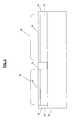
- FIG. 1illustrates a semiconductor structure that can be employed in at least one embodiment of the present application.
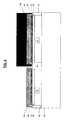
- FIG. 2illustrates the semiconductor structure after it has undergone a shallow trench isolation process, and as a result, contains shallow-trench regions therein, and can also be employed in at least one embodiment of the present application.
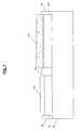
- FIG. 3illustrates the semiconductor structure having a silicon layer in-between a first SiGe layer and a second SiGe layer in a first active region and a second active region, in accordance with an embodiment of the present invention.
- FIG. 4illustrates a mask covering the first active region of the semiconductor structure in accordance with an embodiment of the present invention.
- FIG. 5illustrates the removal of the second SiGe layer from the second active region of the semiconductor structure in accordance with an embodiment of the present invention.
- FIG. 6illustrates the removal of the mask from the first active region of the semiconductor structure in accordance with an embodiment of the present invention.
- FIG. 7illustrates thermal mixing of the first SiGe layer and the silicon layer in the first active region and the thermal mixing of the second SiGe layer, the silicon layer, and the first SiGe layer in the first active region of the semiconductor structure in accordance with an embodiment of the present invention.
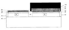
- FIG. 8illustrates the formation of a device in the first active region and a device in the second active region of the semiconductor structure in accordance with an embodiment of the present invention.
- FIG. 1there is illustrated a first exemplary semiconductor structure including, from bottom to top, a handle substrate 40 , a insulator layer 30 and an semiconductor material layer 20 that can be employed in accordance with an embodiment of the present application.
- the handle substrate 40 , the insulator layer 30 and the semiconductor material layer 20may be referred to as an extremely-thin-semiconductor-on-insulator (ETSOI) substrate 10 .
- the semiconductor material layer 20may be referred to as the ETSOI portion of the ETSOI substrate 10 .
- ETSOI substrate 10Although the present application is described and illustrated utilizing an ETSOI substrate 10 , other semiconductor substrates can also be used including, for example, a semiconductor substrate in which handle substrate 40 is omitted.
- the semiconductor material layer 20is present on an uppermost surface of the insulator layer 30 .
- the insulator layer 30is present on an uppermost surface of the handle substrate 40 .
- the handle substrate 40provides mechanical support to the insulator layer 30 and the semiconductor material layer 20 .
- the handle substrate 40 and the semiconductor material layer 20 of the ETSOI substrate 10may comprise a same semiconductor material. In other embodiments of the present application, the handle substrate 40 and the semiconductor material layer 20 of the ETSOI substrate 10 may comprise a different semiconductor material.
- the term “semiconductor” as used herein in connection with the semiconductor material of the handle substrate 40 and the semiconductor material layer 20denotes any semiconducting material including, for example, Si, Ge, SiGe, SiC, SiGeC, InAs, GaAs, InP or other like III/V compound semiconductors. Multilayers of these semiconductor materials can also be used as the semiconductor material of the handle substrate 40 and the semiconductor material layer 20 .
- the handle substrate 40 and the semiconductor material layer 20are both comprised of silicon.
- the handle substrate 40is a non-semiconductor material including, for example, a dielectric material and/or a conductive material.
- the handle substrate 40 and the semiconductor material layer 20may have the same or different crystal orientation.
- the crystal orientation of the handle substrate 40 and/or the semiconductor material layer 20may be ⁇ 100 ⁇ , ⁇ 110 ⁇ , or ⁇ 111 ⁇ . Other crystallographic orientations besides those specifically mentioned can also be used in the present application.
- the handle substrate 40 and/or the semiconductor material layer 20 of the ETSOI substrate 10may be a single crystalline semiconductor material, a polycrystalline material, or an amorphous material.
- at least the semiconductor material layer 20is a single crystalline semiconductor material.
- the semiconductor material layer 20 that is located atop the insulator layer 30can be processed to include semiconductor regions having different crystal orientations.
- the insulator layer 30 of the ETSOI substrate 10may be a crystalline or non-crystalline oxide or nitride.
- the insulator layer 30is an oxide such as, for example, silicon dioxide.
- the insulator layer 30may be continuous or it may be discontinuous. When a discontinuous insulator region is present, the insulator region exists as an isolated island that is surrounded by semiconductor material.
- the thickness of semiconductor material layer 20 of the ETSOI substrate 10is typically from 1 nm to 10 nm, with a thickness from 3 nm to 8 nm being more typical. If the thickness of the semiconductor material layer 20 is not within one of the above mentioned ranges, a thinning step such as, for example, planarization, etching, such as for example, thermal dry or wet oxidation, such as, for example, dry etch or oxidation followed by oxide etch, or any combination thereof, can be used to reduce the thickness of semiconductor material layer 20 to a value within one of the ranges mentioned above.
- a thinning stepsuch as, for example, planarization, etching, such as for example, thermal dry or wet oxidation, such as, for example, dry etch or oxidation followed by oxide etch, or any combination thereof, can be used to reduce the thickness of semiconductor material layer 20 to a value within one of the ranges mentioned above.
- the semiconductor material layer 20should be thin, i.e. less than 8 nm, and even more preferably between 4 nm and 6 nm (or thinned out as required using the processes described above-) and made of pure Silicon or a material comprising primarily Silicon, although it should be reiterated that other variations are possible, including greater dimensions and different material compositions (as may have been mentioned above).
- the insulator layer 30 of the ETSOI substrate 10typically has a thickness from 1 nm to 200 nm, with a thickness from 100 nm to 150 nm being more typical.
- the thickness of the handle substrate 40 of the SOI substratecan vary greatly and remain in accordance with the teaching of the present application.
- the insulator layer 30can be a buried dielectric layer 30 and may be composed of any dielectric material.
- the buried dielectric layer 30may be composed of an oxide, e.g., silicon oxide, a nitride, e.g., silicon nitride, oxynitrides of silicon, e.g. silicon oxynitride, or a combination thereof.
- the buried dielectric layer 30may include crystalline or non-crystalline insulator material.
- the buried dielectric layer 30may be formed using any of several known methods. Non-limiting examples include ion implantation methods, thermal or plasma oxidation or nitridation methods, chemical vapor deposition methods and physical vapor deposition methods.
- the buried dielectric layer 30may have a thickness of 300 nm or less. In another embodiment, the buried dielectric layer 30 may have a thickness ranging from 2 nm to 150 nm. In yet another embodiment, the buried dielectric layer 30 may have a thickness ranging from 5 nm to 30 nm. Preferably, the buried dielectric layer 30 is a buried oxide layer (“BOX”).
- BOXburied oxide layer
- the semiconductor material layer 20may be doped, undoped or contain doped and undoped regions therein. For clarity, the doped regions are not specifically shown in the drawings of the present application. Each doped region within the semiconductor material layer 20 may have the same, or they may have different conductivities and/or doping concentrations.
- the doped regions that are present in the semiconductor material layer 20can be formed by ion implantation process or gas phase doping.
- the semiconductor device of FIG. 1can be processed to include at least one isolation region therein.
- isolation regions 50may be formed in the ETSOI substrate 10 to isolate structures formed on the ETSOI substrate 10 from adjacent structures.
- the ETSOI substrate 10can further include a buried insulator layer 30 , which as stated, can be made of, for example, oxides, nitrides, oxynitrides of silicon, and combinations thereof, and is preferably a buried dielectric layer such as a buried oxide layer (BOX) layer.
- the buried dielectric layer 30may improve device isolation and prevent dopant diffusion.
- Isolation regions 50may be formed by any known method in the art, including, for example, lithography or etching into the ETSOI substrate 10 to form trenches, and then filling the trenches with an insulating material, such as silicon dioxide. After forming isolation regions 50 , an active region 60 in the ETSOI substrate 10 is defined as the region between a pair of isolation regions 50 . Active region 60 may include doped and undoped regions that have been omitted from FIG. 2 for illustrative clarity.
- Other embodimentsmay include other means of isolating structures formed on the ETSOI substrate 10 , or may have isolation around none or only some structures.
- the at least one isolation regionis a shallow trench isolation region (“STI”), but it can be a trench isolation region, a field oxide isolation region (not shown), or any other equivalent known in the art.
- a linermay be formed in the trench prior to trench fill, a densification step may be performed after the trench fill and a planarization process may follow the trench fill as well.
- the field oxide isolation regionmay be formed utilizing a so-called local oxidation of silicon process.
- the at least one isolation regionprovides isolation between neighboring gate structure regions, typically required when the neighboring gates have opposite conductivities, i.e., nFETs and pFETs. As such, the at least one isolation region can separate an nFET device region from a pFET device region.
- a first germanium containing silicon layer (‘a first SiGe layer”) 70is epitaxially grown on each of the active regions 60 .
- the active regionswill not be explicitly identified numerically, and are to be understood as the region between the STI layers, as mentioned above).
- a layer of epitaxial silicon (“Si layer”) 80is deposited over each of the first SiGe layers 70 of the semiconductor substrate.
- the thin Si layer 80can operate as an etch stop layer.
- epitaxial growth and/or depositionand “epitaxially formed and/or grown” mean the growth of a semiconductor material on a deposition surface of a semiconductor material, in which the semiconductor material being grown has the same crystalline characteristics as the semiconductor material of the deposition surface.
- the chemical reactants provided by the source gasesare controlled and the system parameters are set so that the depositing atoms arrive at the deposition surface of the semiconductor substrate with sufficient energy to move around on the surface and orient themselves to the crystal arrangement of the atoms of the deposition surface. Therefore, an epitaxial semiconductor material has the same crystalline characteristics as the deposition surface on which it is formed.
- an epitaxial semiconductor material deposited on a ⁇ 100 ⁇ crystal surfacewill take on a ⁇ 100 ⁇ orientation.
- epitaxial growth and/or deposition processesare selective to forming on semiconductor surface, and do not deposit material on dielectric surfaces, such as silicon dioxide or silicon nitride surfaces.
- Examples of various epitaxial growth process apparatuses that are suitable for use in forming the first germanium containing silicon layer 70 and the second silicon germanium containing silicon layer 80include, e.g., rapid thermal chemical vapor deposition (RTCVD), low-energy plasma deposition (LEPD), ultra-high vacuum chemical vapor deposition (UHVCVD), atmospheric pressure chemical vapor deposition (APCVD) and molecular beam epitaxy (MBE).
- RTCVDrapid thermal chemical vapor deposition
- LEPDlow-energy plasma deposition
- UHVCVDultra-high vacuum chemical vapor deposition
- APCVDatmospheric pressure chemical vapor deposition
- MBEmolecular beam epitaxy
- the temperature for epitaxial deposition process for forming germanium containing silicon layer 70 and the second silicon germanium containing silicon layer 80typically ranges from 550° C. to 900° C. Although higher temperature typically results in faster deposition, the faster deposition may result in crystal defects and film cracking.
- the gas source for the deposition of epitaxial semiconductor materialinclude a silicon containing gas source, a germanium containing gas source, or a combination thereof.
- an epitaxial Si layermay be deposited from a silicon gas source that is selected from the group consisting of silane, disilane, trisilane, tetrasilane, hexachlorodisilane, tetrachlorosilane, dichlorosilane, trichlorosilane, methylsilane, dimethylsilane, ethylsilane, methyldisilane, dimethyldisilane, hexamethyldisilane and combinations thereof.
- a silicon gas sourcethat is selected from the group consisting of silane, disilane, trisilane, tetrasilane, hexachlorodisilane, tetrachlorosilane, dichlorosilane, trichlorosilane, methylsilane, dimethylsilane, ethylsilane, methyldisilane, dimethyldisilane, hexamethyldisilane and combinations thereof.
- An epitaxial germanium layercan be deposited from a germanium gas source that is selected from the group consisting of germane, digermane, halogermane, dichlorogermane, trichlorogermane, tetrachlorogermane and combinations thereof. While an epitaxial silicon germanium alloy layer can be formed utilizing a combination of such gas sources. Carrier gases like hydrogen, nitrogen, helium and argon can be used.
- a second germanium containing silicon layer 90(“a second SiGe layer”) is epitaxially deposited over each of the Si layers 80 that are over the first SiGe layers 70 .
- the thickness of each of the first SiGe layers 70 , the Si layer 80 , and the second SiGe layers 90 and the concentration of Germanium in both the first SiGe layers 70 and the second SiGe layers 90are chosen with a final product in mind, where higher germanium concentration leads to increased electron mobility, and as a general matter, different germanium concentrations allow one to tune the threshold voltage of a given device. As such, and as may be mentioned elsewhere below, the parameters mentioned in the preceding sentence are determined based on the physical properties desired in a final product.
- the first SiGe layer 70will have a different thickness and/or concentration of Germanium than the second SiGe layer 90 , and in other embodiments, the first SiGe layer 70 will have the same concentration of Germanium and/or the same thickness. This will be discussed in greater detail below.
- Epitaxial growth of the first SiGe layer 70 and the second SiGe layer 90is preferably uniform.
- the above process stepscan all be performed in the same epitaxial reactor, in the same recipe during the same process run by starting with growth of the first SiGe layer 70 , followed by growing the thin Si layer 80 and then continuing with the growth of the second SiGe layer 90 .
- This featureincreases efficiency and promotes economic advantage, i.e. cost reduction, by eliminating the need for an additional process run.
- the presence of the Si layer 80operates as an etch stop layer as will later be shown, and obviates masking of one of the active regions while epitaxially growing the second SiGe layer 90 , i.e. the second epitaxial layer, on the other active region.
- Processing all process steps in one process runeliminates a second independent epitaxy process run, including an epitaxial prebake to preclean the semiconductor surfaces for epitaxial processing.
- the prebake and preclean processare more challenging for SiGe than for Silicon due to the strain in the SiGe layers on Silicon and the tendency of strained SiGe to relax and to form defects during high temperature processing.
- the presence of the Si layer 80enables the ability to form the first SiGe layer 70 , the Si layer 80 , and the second SiGe layer 90 in a single process run; where epitaxial single process run means a continuous epitaxial growth process in a single epitaxial reactor, without requiring removing the ETSOI substrate 10 and reinstalling it in the same or another epitaxial reactor for further epitaxial processing.
- FIG. 4another aspect of and embodiment of the invention is shown.
- a hard mask 100is deposited over one of the active regions.
- FIGS. 3-7show some lateral overgrowth with respect to the active region 30 from one or both of the SiGe layers; however, in application, the overgrowth can be negligible or non-existent.
- the hard mask materialcan be, for example, silicon nitride and/or silicon dioxide.
- the second SiGe layer 90 of one of the unmasked active regionsis removed.
- the removal of the SiGe layercan be by gaseous HCl etch or by wet etch processing, i.e. with TMAH. Gaseous HCl etch removal is the preferred method.
- the SiGe layers of the other active regionare protected by the hardmask 100 .
- the hardmask 100 covering one of the active regionsis removed.
- FIG. 7another aspect of an embodiment of the invention is shown. Specifically, after the hardmask 100 is removed, the Si layer 80 and the first SiGe layer 70 remain for one of the active regions, the second SiGe layer 90 having been removed, and the Si layer 80 and both the first SiGe layer 70 and the second SiGe layer 90 of the other one of the active regions remains in place.
- the remaining layers on each active regioncan be thermally mixed by thermally annealing them. Specifically, in the active region that has the second SiGe layer 90 removed, the semiconductor material layer 20 of the ETSOI substrate 10 in that region, the first SiGe layer 70 , and the Si layer 80 will thermally mix to form one final, merged, SiGe layer 110 .
- the anneal processcan be furnace anneal, rapid thermal anneal, flash anneal, or any suitable combination of those processes.
- the anneal temperatureranges from 600 degrees to 1300 degrees Centigrade.
- the anneal timeranges from 1 millisecond to 2 hours, depending on the anneal temperature. Higher anneal temperatures require shorter anneal times.
- a typical anneal conditionis about 30 minutes at 1000° C.
- such annealingcauses the mixing of the first SiGe layer 70 and the Si 80 layer of one active region and the semiconductor material layer 20 of the ETSOI substrate 10 in that region, forming one merged SiGe layer 110 on one of the active regions. Furthermore, such annealing causes the mixing of the first SiGe layer 70 , the Si 80 layer, the semiconductor material layer 20 of the ETSOI substrate 10 in that region and the second SiGe layer 90 of the other active region and the semiconductor material layer 20 of the ETSOI substrate 10 in that region, forming another merged SiGe layer 120 on one of the active regions.
- two active regions with ETSGOI layers 110 and 120 with different Germanium concentrationsare formed. Accordingly, one aspect of an embodiment of the present invention produces a substrate that has active regions with two distinct SiGe layers with different Germanium concentrations.
- the resulting merged SiGe layer 110which had its second SiGe layer removed, will usually have a lower Germanium content than the first SiGe layer 70 before the mixing.
- the reason for thisis that the thin Si layer 80 and the semiconductor material layer 20 of the ETSOI substrate 10 reduce the overall Germanium content when mixed with the first SiGe layer 70 . (This is the case when the semiconductor material layer 20 is pure silicon or primarily silicon).
- the thermal annealing of the layers of the other active regionsince the first SiGe layer 70 , the Si layer 80 , the second SiGe layer 90 and the ETSOI 20 will be thermally mixed, it is possible, depending on the selection of the thickness of each of the layers and the concentration of Germanium in each of the SiGe layers, for the second merged SiGe layer 120 to have a higher or lower concentration of Germanium than each of the first SiGe layer 70 and the second SiGe layer 90 , which were originally present in the active regions.
- the final Germanium content of the final merged layers 110 and 120by selecting the thickness of the ETSOI layer 20 and the thin Si layer 80 , and by selecting the thickness and/or the Germanium concentration of the First SiGe layer 70 and the second SiGe layer 80 ; however, the final two thermally mixed SiGe layers, SiGe layer 110 and SiGe layer 120 , will usually have different Germanium contents because one of the active regions at the thermal mixing stage has the extra SiGe layer 90 .
- Germanium content of the final thermally mixed silicon germanium layerscan be engineered as desired for particular applications by ensuring that the initial deposited germanium containing layers have an appropriate germanium content and/or thickness for the particular application desired.
- the thin Si layer 80will be very thin, ranging from 1-2 nm.
- the thin Si layer 80is between 1-2 nm, substantial benefit is obtained in that it reduces the dilution effect on the overall SiGe concentration while still affording some of the benefits of the described herein, including the reduced process steps, which is possible at least due to the thin Si layer's 80 function as an etch stop layer.
- the thickness of the semiconductor material layer 20 of the ETSOI substrate 10is 6 nm
- the thickness of the first SiGe layer 70 of both active regionsis 4 nm, with a Germanium concentration of 35%
- the thickness of the thin Si layer 80is 2 nm
- the thickness of the second SiGe layer 90is 5 nm, with a Germanium concentration of 60%.
- one active regionAfter undergoing the process steps described above, including the removal of the second SiGe layer 90 for one of the active regions and the thermal mixing of the various layers as described above, one active region will have a final merged SiGe layer 110 with a thickness of 12 nm and a Germanium concentration of about 12%, and the other active region will have a final merged SiGe layer 120 with a thickness of 17 nm and a Germanium concentration of about 25%.
- the thickness of the semiconductor material layer 20 of the ETSOI substrate 10is 4 nm
- the thickness of the first SiGe layer 70 of both active regionsis 6 nm, with a Germanium concentration of 40%
- the thickness of the thin Si layer 80is 2 nm
- the thickness of the second SiGe layer 90is 6 nm, with a Germanium concentration of 40%.
- one active regionAfter undergoing the process steps described above, including the removal of the second SiGe layer 90 for one of the active regions and the thermal mixing of the various layers as described above, one active region will have a final merged SiGe layer 110 with a thickness of 12 nm and a Germanium concentration of about 20%, and the other active region will have a final merged SiGe layer 120 with a thickness of 18 nm and a Germanium concentration of about 33%.
- the particular embodimentshave both the first SiGe layer 70 and the second SiGe layer 90 as being of the same thickness, it is possible to arrive at configurations where the thicknesses differ from one another. It is also possible to vary the thickness of the thin Si layer 80 and the semiconductor material layer 20 of the ETSOI substrate 10 in relation to one another and in relation to the SiGe layers. The same applies with respect with the initial concentration of the germanium content of the first SiGe layer 70 and the second SiGe layer 90 , i.e. they do not have to be the same.
- one of the SiGe layershas the same thickness as the semiconductor material layer 20 of the ETSOI substrate 10 . In one embodiment, one of the SiGe layers has a thickness that is less than the semiconductor material layer 20 of the ETSOI substrate 10 . In yet another embodiment, one of the SiGe layers has a thickness that is greater than the semiconductor material layer 20 of the ETSOI substrate 10 .
- the semiconductor material layer 20 of the ETSOI substrate 10which as stated is preferably made of pure silicon or a material primarily made of silicon, and whether it is of the same as one of the SiGe layers or otherwise, is made as thin as possible, i.e. 3-4 nm, to reduce the amount of dilution from the pure silicon in forming higher percentage SiGe layers.
- FIG. 8another aspect of the invention is shown.
- devicesmay be placed over layer 110 and 120 .
- two pFET devicesare shown 130 and 140 devices are provided as the examples in FIG. 8 .
Landscapes
- Engineering & Computer Science (AREA)
- Microelectronics & Electronic Packaging (AREA)
- Condensed Matter Physics & Semiconductors (AREA)
- General Physics & Mathematics (AREA)
- Manufacturing & Machinery (AREA)
- Computer Hardware Design (AREA)
- Physics & Mathematics (AREA)
- Power Engineering (AREA)
- Chemical & Material Sciences (AREA)
- Crystallography & Structural Chemistry (AREA)
- Metal-Oxide And Bipolar Metal-Oxide Semiconductor Integrated Circuits (AREA)
- Insulated Gate Type Field-Effect Transistor (AREA)
- Thin Film Transistor (AREA)
- Recrystallisation Techniques (AREA)
Abstract
Description
Claims (16)
Priority Applications (2)
| Application Number | Priority Date | Filing Date | Title |
|---|---|---|---|
| US14/096,120US8987069B1 (en) | 2013-12-04 | 2013-12-04 | Semiconductor substrate with multiple SiGe regions having different germanium concentrations by a single epitaxy process |
| US14/595,311US20150155301A1 (en) | 2013-12-04 | 2015-01-13 | SEMICONDUCTOR SUBSTRATE WITH MULTIPLE SiGe REGIONS HAVING DIFFERENT GERMANIUM CONCENTRATIONS BY A SINGLE EPITAXY PROCESS |
Applications Claiming Priority (1)
| Application Number | Priority Date | Filing Date | Title |
|---|---|---|---|
| US14/096,120US8987069B1 (en) | 2013-12-04 | 2013-12-04 | Semiconductor substrate with multiple SiGe regions having different germanium concentrations by a single epitaxy process |
Related Child Applications (1)
| Application Number | Title | Priority Date | Filing Date |
|---|---|---|---|
| US14/595,311DivisionUS20150155301A1 (en) | 2013-12-04 | 2015-01-13 | SEMICONDUCTOR SUBSTRATE WITH MULTIPLE SiGe REGIONS HAVING DIFFERENT GERMANIUM CONCENTRATIONS BY A SINGLE EPITAXY PROCESS |
Publications (1)
| Publication Number | Publication Date |
|---|---|
| US8987069B1true US8987069B1 (en) | 2015-03-24 |
Family
ID=52683271
Family Applications (2)
| Application Number | Title | Priority Date | Filing Date |
|---|---|---|---|
| US14/096,120ActiveUS8987069B1 (en) | 2013-12-04 | 2013-12-04 | Semiconductor substrate with multiple SiGe regions having different germanium concentrations by a single epitaxy process |
| US14/595,311AbandonedUS20150155301A1 (en) | 2013-12-04 | 2015-01-13 | SEMICONDUCTOR SUBSTRATE WITH MULTIPLE SiGe REGIONS HAVING DIFFERENT GERMANIUM CONCENTRATIONS BY A SINGLE EPITAXY PROCESS |
Family Applications After (1)
| Application Number | Title | Priority Date | Filing Date |
|---|---|---|---|
| US14/595,311AbandonedUS20150155301A1 (en) | 2013-12-04 | 2015-01-13 | SEMICONDUCTOR SUBSTRATE WITH MULTIPLE SiGe REGIONS HAVING DIFFERENT GERMANIUM CONCENTRATIONS BY A SINGLE EPITAXY PROCESS |
Country Status (1)
| Country | Link |
|---|---|
| US (2) | US8987069B1 (en) |
Cited By (10)
| Publication number | Priority date | Publication date | Assignee | Title |
|---|---|---|---|---|
| US20150318216A1 (en)* | 2014-05-01 | 2015-11-05 | International Business Machines Corporation | Formation of germanium-containing channel region by thermal condensation utilizing an oxygen permeable material |
| US20160056269A1 (en)* | 2014-08-22 | 2016-02-25 | Samsung Electronics Co., Ltd. | Method of fabricating a semiconductor device |
| US9659960B1 (en)* | 2015-12-09 | 2017-05-23 | International Business Machines Corporation | Extremely thin silicon-on-insulator silicon germanium device without edge strain relaxation |
| US9685510B2 (en) | 2015-09-10 | 2017-06-20 | International Business Machines Corporation | SiGe CMOS with tensely strained NFET and compressively strained PFET |
| US9755078B2 (en) | 2015-10-23 | 2017-09-05 | International Business Machines Corporation | Structure and method for multi-threshold voltage adjusted silicon germanium alloy devices with same silicon germanium content |
| US9812571B2 (en) | 2015-09-30 | 2017-11-07 | International Business Machines Corporation | Tensile strained high percentage silicon germanium alloy FinFETs |
| US9922984B1 (en) | 2016-09-22 | 2018-03-20 | International Business Machines Corporation | Threshold voltage modulation through channel length adjustment |
| US20190312041A1 (en)* | 2018-04-04 | 2019-10-10 | Globalfoundries Inc. | Semiconductor devices including si/ge active regions with different ge concentrations |
| US10559593B1 (en) | 2018-08-13 | 2020-02-11 | Globalfoundries Inc. | Field-effect transistors with a grown silicon-germanium channel |
| US11699757B2 (en)* | 2014-01-31 | 2023-07-11 | Stmicroelectronics, Inc. | High dose implantation for ultrathin semiconductor-on-insulator substrates |
Families Citing this family (1)
| Publication number | Priority date | Publication date | Assignee | Title |
|---|---|---|---|---|
| US12317578B2 (en)* | 2022-06-07 | 2025-05-27 | Taiwan Semiconductor Manufacturing Company, Ltd. | Semiconductor devices with low leakage current and methods of fabricating the same |
Citations (12)
| Publication number | Priority date | Publication date | Assignee | Title |
|---|---|---|---|---|
| US6515335B1 (en)* | 2002-01-04 | 2003-02-04 | International Business Machines Corporation | Method for fabrication of relaxed SiGe buffer layers on silicon-on-insulators and structures containing the same |
| US6649492B2 (en) | 2002-02-11 | 2003-11-18 | International Business Machines Corporation | Strained Si based layer made by UHV-CVD, and devices therein |
| US6709912B1 (en) | 2002-10-08 | 2004-03-23 | Chartered Semiconductor Manufacturing Ltd. | Dual Si-Ge polysilicon gate with different Ge concentrations for CMOS device optimization |
| US6861304B2 (en) | 1999-11-01 | 2005-03-01 | Hitachi, Ltd. | Semiconductor integrated circuit device and method of manufacturing thereof |
| US6969875B2 (en)* | 2000-05-26 | 2005-11-29 | Amberwave Systems Corporation | Buried channel strained silicon FET using a supply layer created through ion implantation |
| US20060042542A1 (en)* | 2004-09-02 | 2006-03-02 | International Business Machines Corporation | Method of producing silicon-germanium-on-insulator material using unstrained Ge-containing source layers |
| US7198995B2 (en) | 2003-12-12 | 2007-04-03 | International Business Machines Corporation | Strained finFETs and method of manufacture |
| US7547605B2 (en) | 2004-11-22 | 2009-06-16 | Taiwan Semiconductor Manufacturing Company | Microelectronic device and a method for its manufacture |
| US20100068869A1 (en) | 2008-09-18 | 2010-03-18 | Commissariat A L'energie Atomique | Method for fabricating a micro-electronic device equipped with semi-conductor zones on an insulator with a horizontal ge concentration gradient |
| JP2010171282A (en) | 2009-01-23 | 2010-08-05 | Sumco Techxiv株式会社 | SEMICONDUCTOR SUBSTRATE, METHOD OF MANUFACTURING THE SAME, AND Si-SiGe STACK |
| US8110486B2 (en)* | 2006-01-18 | 2012-02-07 | Sumco Corporation | Method of manufacturing semiconductor wafer by forming a strain relaxation SiGe layer on an insulating layer of SOI wafer |
| US20120038006A1 (en) | 2009-12-30 | 2012-02-16 | Institute of Microelectronics, Chinese Academy of Sciences | Semiconductor device and method for manufacturing the same |
Family Cites Families (7)
| Publication number | Priority date | Publication date | Assignee | Title |
|---|---|---|---|---|
| KR100495023B1 (en)* | 2000-12-28 | 2005-06-14 | 가부시끼가이샤 도시바 | A semiconductor device and manufacturing method thereof |
| US6963078B2 (en)* | 2003-03-15 | 2005-11-08 | International Business Machines Corporation | Dual strain-state SiGe layers for microelectronics |
| US7393733B2 (en)* | 2004-12-01 | 2008-07-01 | Amberwave Systems Corporation | Methods of forming hybrid fin field-effect transistor structures |
| US7220626B2 (en)* | 2005-01-28 | 2007-05-22 | International Business Machines Corporation | Structure and method for manufacturing planar strained Si/SiGe substrate with multiple orientations and different stress levels |
| FR2902234B1 (en)* | 2006-06-12 | 2008-10-10 | Commissariat Energie Atomique | METHOD FOR MAKING Si1-yGey ZONES OF DIFFERENT Ge CONTENTS ON THE SAME SUBSTRATE BY GERMANIUM CONDENSATION |
| KR101299646B1 (en)* | 2006-10-12 | 2013-08-26 | 삼성디스플레이 주식회사 | Display panel and method of manufacturing the same |
| US8106381B2 (en)* | 2006-10-18 | 2012-01-31 | Translucent, Inc. | Semiconductor structures with rare-earths |
- 2013
- 2013-12-04USUS14/096,120patent/US8987069B1/enactiveActive
- 2015
- 2015-01-13USUS14/595,311patent/US20150155301A1/ennot_activeAbandoned
Patent Citations (12)
| Publication number | Priority date | Publication date | Assignee | Title |
|---|---|---|---|---|
| US6861304B2 (en) | 1999-11-01 | 2005-03-01 | Hitachi, Ltd. | Semiconductor integrated circuit device and method of manufacturing thereof |
| US6969875B2 (en)* | 2000-05-26 | 2005-11-29 | Amberwave Systems Corporation | Buried channel strained silicon FET using a supply layer created through ion implantation |
| US6515335B1 (en)* | 2002-01-04 | 2003-02-04 | International Business Machines Corporation | Method for fabrication of relaxed SiGe buffer layers on silicon-on-insulators and structures containing the same |
| US6649492B2 (en) | 2002-02-11 | 2003-11-18 | International Business Machines Corporation | Strained Si based layer made by UHV-CVD, and devices therein |
| US6709912B1 (en) | 2002-10-08 | 2004-03-23 | Chartered Semiconductor Manufacturing Ltd. | Dual Si-Ge polysilicon gate with different Ge concentrations for CMOS device optimization |
| US7198995B2 (en) | 2003-12-12 | 2007-04-03 | International Business Machines Corporation | Strained finFETs and method of manufacture |
| US20060042542A1 (en)* | 2004-09-02 | 2006-03-02 | International Business Machines Corporation | Method of producing silicon-germanium-on-insulator material using unstrained Ge-containing source layers |
| US7547605B2 (en) | 2004-11-22 | 2009-06-16 | Taiwan Semiconductor Manufacturing Company | Microelectronic device and a method for its manufacture |
| US8110486B2 (en)* | 2006-01-18 | 2012-02-07 | Sumco Corporation | Method of manufacturing semiconductor wafer by forming a strain relaxation SiGe layer on an insulating layer of SOI wafer |
| US20100068869A1 (en) | 2008-09-18 | 2010-03-18 | Commissariat A L'energie Atomique | Method for fabricating a micro-electronic device equipped with semi-conductor zones on an insulator with a horizontal ge concentration gradient |
| JP2010171282A (en) | 2009-01-23 | 2010-08-05 | Sumco Techxiv株式会社 | SEMICONDUCTOR SUBSTRATE, METHOD OF MANUFACTURING THE SAME, AND Si-SiGe STACK |
| US20120038006A1 (en) | 2009-12-30 | 2012-02-16 | Institute of Microelectronics, Chinese Academy of Sciences | Semiconductor device and method for manufacturing the same |
Cited By (24)
| Publication number | Priority date | Publication date | Assignee | Title |
|---|---|---|---|---|
| US12432987B2 (en) | 2014-01-31 | 2025-09-30 | Stmicroelectronics, Inc. | High dose implantation for ultrathin semiconductor-on-insulator substrates |
| US11699757B2 (en)* | 2014-01-31 | 2023-07-11 | Stmicroelectronics, Inc. | High dose implantation for ultrathin semiconductor-on-insulator substrates |
| US9583378B2 (en)* | 2014-05-01 | 2017-02-28 | International Business Machines Corporation | Formation of germanium-containing channel region by thermal condensation utilizing an oxygen permeable material |
| US20150318216A1 (en)* | 2014-05-01 | 2015-11-05 | International Business Machines Corporation | Formation of germanium-containing channel region by thermal condensation utilizing an oxygen permeable material |
| US9508832B2 (en)* | 2014-08-22 | 2016-11-29 | Samsung Electronics Co., Ltd. | Method of fabricating a semiconductor device |
| US20160056269A1 (en)* | 2014-08-22 | 2016-02-25 | Samsung Electronics Co., Ltd. | Method of fabricating a semiconductor device |
| US9685510B2 (en) | 2015-09-10 | 2017-06-20 | International Business Machines Corporation | SiGe CMOS with tensely strained NFET and compressively strained PFET |
| US9812571B2 (en) | 2015-09-30 | 2017-11-07 | International Business Machines Corporation | Tensile strained high percentage silicon germanium alloy FinFETs |
| US10211341B2 (en) | 2015-09-30 | 2019-02-19 | International Business Machines Corporation | Tensile strained high percentage silicon germanium alloy FinFETS |
| US9755078B2 (en) | 2015-10-23 | 2017-09-05 | International Business Machines Corporation | Structure and method for multi-threshold voltage adjusted silicon germanium alloy devices with same silicon germanium content |
| US10340292B2 (en) | 2015-12-09 | 2019-07-02 | International Business Machines Corporation | Extremely thin silicon-on-insulator silicon germanium device without edge strain relaxation |
| US9659960B1 (en)* | 2015-12-09 | 2017-05-23 | International Business Machines Corporation | Extremely thin silicon-on-insulator silicon germanium device without edge strain relaxation |
| US9853054B2 (en) | 2015-12-09 | 2017-12-26 | International Business Machines Corporation | Extremely thin silicon-on-insulator silicon germanium device without edge strain relaxation |
| US10115805B2 (en) | 2015-12-09 | 2018-10-30 | International Business Machines Corporation | Extremely thin silicon-on-insulator silicon germanium device without edge strain relaxation |
| US10658387B2 (en) | 2015-12-09 | 2020-05-19 | International Business Machines Corporation | Extremely thin silicon-on-insulator silicon germanium device without edge strain relaxation |
| US10170593B2 (en) | 2016-09-22 | 2019-01-01 | International Business Machines Corporation | Threshold voltage modulation through channel length adjustment |
| US10263098B2 (en) | 2016-09-22 | 2019-04-16 | International Business Machines Corporation | Threshold voltage modulation through channel length adjustment |
| US10224419B2 (en) | 2016-09-22 | 2019-03-05 | International Business Machines Corporation | Threshold voltage modulation through channel length adjustment |
| US9922983B1 (en) | 2016-09-22 | 2018-03-20 | International Business Machines Corporation | Threshold voltage modulation through channel length adjustment |
| US9922984B1 (en) | 2016-09-22 | 2018-03-20 | International Business Machines Corporation | Threshold voltage modulation through channel length adjustment |
| US20190312041A1 (en)* | 2018-04-04 | 2019-10-10 | Globalfoundries Inc. | Semiconductor devices including si/ge active regions with different ge concentrations |
| US10522555B2 (en)* | 2018-04-04 | 2019-12-31 | Globalfoundries Inc. | Semiconductor devices including Si/Ge active regions with different Ge concentrations |
| US11031406B2 (en)* | 2018-04-04 | 2021-06-08 | Globalfoundries U.S. Inc. | Semiconductor devices having silicon/germanium active regions with different germanium concentrations |
| US10559593B1 (en) | 2018-08-13 | 2020-02-11 | Globalfoundries Inc. | Field-effect transistors with a grown silicon-germanium channel |
Also Published As
| Publication number | Publication date |
|---|---|
| US20150155301A1 (en) | 2015-06-04 |
Similar Documents
| Publication | Publication Date | Title |
|---|---|---|
| US8987069B1 (en) | Semiconductor substrate with multiple SiGe regions having different germanium concentrations by a single epitaxy process | |
| US7247534B2 (en) | Silicon device on Si:C-OI and SGOI and method of manufacture | |
| US7439110B2 (en) | Strained HOT (hybrid orientation technology) MOSFETs | |
| US9859369B2 (en) | Semiconductor device including nanowire transistors with hybrid channels | |
| US7670934B1 (en) | Methods for fabricating MOS devices having epitaxially grown stress-inducing source and drain regions | |
| US10153157B2 (en) | P-FET with graded silicon-germanium channel | |
| US7544548B2 (en) | Trench liner for DSO integration | |
| US10079303B2 (en) | Method to form strained nFET and strained pFET nanowires on a same substrate | |
| US9786547B2 (en) | Channel silicon germanium formation method | |
| US8951868B1 (en) | Formation of functional gate structures with different critical dimensions using a replacement gate process | |
| US9129938B1 (en) | Methods of forming germanium-containing and/or III-V nanowire gate-all-around transistors | |
| CN105762080A (en) | Electrically Insulated Fin Structure(s) With Alternative Channel Materials And Fabrication Methods | |
| EP1709671A1 (en) | Method of forming thin sgoi wafers with high relaxation and low stacking fault defect density | |
| US20140252501A1 (en) | Sacrificial replacement extension layer to obtain abrupt doping profile | |
| US7495266B2 (en) | Strained silicon-on-silicon by wafer bonding and layer transfer | |
| US9356019B2 (en) | Integrated circuit with on chip planar diode and CMOS devices | |
| US20170179127A1 (en) | Semiconductor structure having silicon germanium fins and method of fabricating same | |
| US20190181052A1 (en) | FORMATION OF COMMON INTERFACIAL LAYER ON Si/SiGe DUAL CHANNEL COMPLEMENTARY METAL OXIDE SEMICONDUCTOR DEVICE | |
| US8440539B2 (en) | Isolation trench processing for strain control | |
| US9209065B1 (en) | Engineered substrate and device for co-integration of strained silicon and relaxed silicon |
Legal Events
| Date | Code | Title | Description |
|---|---|---|---|
| AS | Assignment | Owner name:INTERNATIONAL BUSINESS MACHINES CORPORATION, NEW Y Free format text:ASSIGNMENT OF ASSIGNORS INTEREST;ASSIGNORS:ADAM, THOMAS N.;CHENG, KANGGUO;KHAKIFIROOZ, ALI;AND OTHERS;SIGNING DATES FROM 20131029 TO 20131030;REEL/FRAME:031711/0453 | |
| STCF | Information on status: patent grant | Free format text:PATENTED CASE | |
| AS | Assignment | Owner name:GLOBALFOUNDRIES U.S. 2 LLC, NEW YORK Free format text:ASSIGNMENT OF ASSIGNORS INTEREST;ASSIGNOR:INTERNATIONAL BUSINESS MACHINES CORPORATION;REEL/FRAME:036550/0001 Effective date:20150629 | |
| AS | Assignment | Owner name:GLOBALFOUNDRIES INC., CAYMAN ISLANDS Free format text:ASSIGNMENT OF ASSIGNORS INTEREST;ASSIGNORS:GLOBALFOUNDRIES U.S. 2 LLC;GLOBALFOUNDRIES U.S. INC.;REEL/FRAME:036779/0001 Effective date:20150910 | |
| MAFP | Maintenance fee payment | Free format text:PAYMENT OF MAINTENANCE FEE, 4TH YEAR, LARGE ENTITY (ORIGINAL EVENT CODE: M1551); ENTITY STATUS OF PATENT OWNER: LARGE ENTITY Year of fee payment:4 | |
| AS | Assignment | Owner name:WILMINGTON TRUST, NATIONAL ASSOCIATION, DELAWARE Free format text:SECURITY AGREEMENT;ASSIGNOR:GLOBALFOUNDRIES INC.;REEL/FRAME:049490/0001 Effective date:20181127 | |
| AS | Assignment | Owner name:GLOBALFOUNDRIES U.S. INC., CALIFORNIA Free format text:ASSIGNMENT OF ASSIGNORS INTEREST;ASSIGNOR:GLOBALFOUNDRIES INC.;REEL/FRAME:054633/0001 Effective date:20201022 | |
| AS | Assignment | Owner name:GLOBALFOUNDRIES INC., CAYMAN ISLANDS Free format text:RELEASE BY SECURED PARTY;ASSIGNOR:WILMINGTON TRUST, NATIONAL ASSOCIATION;REEL/FRAME:054636/0001 Effective date:20201117 | |
| AS | Assignment | Owner name:GLOBALFOUNDRIES U.S. INC., NEW YORK Free format text:RELEASE BY SECURED PARTY;ASSIGNOR:WILMINGTON TRUST, NATIONAL ASSOCIATION;REEL/FRAME:056987/0001 Effective date:20201117 | |
| MAFP | Maintenance fee payment | Free format text:PAYMENT OF MAINTENANCE FEE, 8TH YEAR, LARGE ENTITY (ORIGINAL EVENT CODE: M1552); ENTITY STATUS OF PATENT OWNER: LARGE ENTITY Year of fee payment:8 |