US8986451B2 - Linear batch chemical vapor deposition system - Google Patents
Linear batch chemical vapor deposition systemDownload PDFInfo
- Publication number
- US8986451B2 US8986451B2US12/787,082US78708210AUS8986451B2US 8986451 B2US8986451 B2US 8986451B2US 78708210 AUS78708210 AUS 78708210AUS 8986451 B2US8986451 B2US 8986451B2
- Authority
- US
- United States
- Prior art keywords
- linear
- planar disc
- receptacles
- substrate carrier
- substrate
- Prior art date
- Legal status (The legal status is an assumption and is not a legal conclusion. Google has not performed a legal analysis and makes no representation as to the accuracy of the status listed.)
- Expired - Fee Related, expires
Links
Images


Classifications
- C—CHEMISTRY; METALLURGY
- C23—COATING METALLIC MATERIAL; COATING MATERIAL WITH METALLIC MATERIAL; CHEMICAL SURFACE TREATMENT; DIFFUSION TREATMENT OF METALLIC MATERIAL; COATING BY VACUUM EVAPORATION, BY SPUTTERING, BY ION IMPLANTATION OR BY CHEMICAL VAPOUR DEPOSITION, IN GENERAL; INHIBITING CORROSION OF METALLIC MATERIAL OR INCRUSTATION IN GENERAL
- C23C—COATING METALLIC MATERIAL; COATING MATERIAL WITH METALLIC MATERIAL; SURFACE TREATMENT OF METALLIC MATERIAL BY DIFFUSION INTO THE SURFACE, BY CHEMICAL CONVERSION OR SUBSTITUTION; COATING BY VACUUM EVAPORATION, BY SPUTTERING, BY ION IMPLANTATION OR BY CHEMICAL VAPOUR DEPOSITION, IN GENERAL
- C23C16/00—Chemical coating by decomposition of gaseous compounds, without leaving reaction products of surface material in the coating, i.e. chemical vapour deposition [CVD] processes
- C23C16/44—Chemical coating by decomposition of gaseous compounds, without leaving reaction products of surface material in the coating, i.e. chemical vapour deposition [CVD] processes characterised by the method of coating
- C23C16/458—Chemical coating by decomposition of gaseous compounds, without leaving reaction products of surface material in the coating, i.e. chemical vapour deposition [CVD] processes characterised by the method of coating characterised by the method used for supporting substrates in the reaction chamber
- C23C16/4582—Rigid and flat substrates, e.g. plates or discs
- C23C16/4583—Rigid and flat substrates, e.g. plates or discs the substrate being supported substantially horizontally
- C23C16/4584—Rigid and flat substrates, e.g. plates or discs the substrate being supported substantially horizontally the substrate being rotated
- C—CHEMISTRY; METALLURGY
- C23—COATING METALLIC MATERIAL; COATING MATERIAL WITH METALLIC MATERIAL; CHEMICAL SURFACE TREATMENT; DIFFUSION TREATMENT OF METALLIC MATERIAL; COATING BY VACUUM EVAPORATION, BY SPUTTERING, BY ION IMPLANTATION OR BY CHEMICAL VAPOUR DEPOSITION, IN GENERAL; INHIBITING CORROSION OF METALLIC MATERIAL OR INCRUSTATION IN GENERAL
- C23C—COATING METALLIC MATERIAL; COATING MATERIAL WITH METALLIC MATERIAL; SURFACE TREATMENT OF METALLIC MATERIAL BY DIFFUSION INTO THE SURFACE, BY CHEMICAL CONVERSION OR SUBSTITUTION; COATING BY VACUUM EVAPORATION, BY SPUTTERING, BY ION IMPLANTATION OR BY CHEMICAL VAPOUR DEPOSITION, IN GENERAL
- C23C16/00—Chemical coating by decomposition of gaseous compounds, without leaving reaction products of surface material in the coating, i.e. chemical vapour deposition [CVD] processes
- C23C16/44—Chemical coating by decomposition of gaseous compounds, without leaving reaction products of surface material in the coating, i.e. chemical vapour deposition [CVD] processes characterised by the method of coating
- C23C16/455—Chemical coating by decomposition of gaseous compounds, without leaving reaction products of surface material in the coating, i.e. chemical vapour deposition [CVD] processes characterised by the method of coating characterised by the method used for introducing gases into reaction chamber or for modifying gas flows in reaction chamber
- C23C16/45563—Gas nozzles
- C23C16/45565—Shower nozzles
- C—CHEMISTRY; METALLURGY
- C23—COATING METALLIC MATERIAL; COATING MATERIAL WITH METALLIC MATERIAL; CHEMICAL SURFACE TREATMENT; DIFFUSION TREATMENT OF METALLIC MATERIAL; COATING BY VACUUM EVAPORATION, BY SPUTTERING, BY ION IMPLANTATION OR BY CHEMICAL VAPOUR DEPOSITION, IN GENERAL; INHIBITING CORROSION OF METALLIC MATERIAL OR INCRUSTATION IN GENERAL
- C23C—COATING METALLIC MATERIAL; COATING MATERIAL WITH METALLIC MATERIAL; SURFACE TREATMENT OF METALLIC MATERIAL BY DIFFUSION INTO THE SURFACE, BY CHEMICAL CONVERSION OR SUBSTITUTION; COATING BY VACUUM EVAPORATION, BY SPUTTERING, BY ION IMPLANTATION OR BY CHEMICAL VAPOUR DEPOSITION, IN GENERAL
- C23C16/00—Chemical coating by decomposition of gaseous compounds, without leaving reaction products of surface material in the coating, i.e. chemical vapour deposition [CVD] processes
- C23C16/44—Chemical coating by decomposition of gaseous compounds, without leaving reaction products of surface material in the coating, i.e. chemical vapour deposition [CVD] processes characterised by the method of coating
- C23C16/455—Chemical coating by decomposition of gaseous compounds, without leaving reaction products of surface material in the coating, i.e. chemical vapour deposition [CVD] processes characterised by the method of coating characterised by the method used for introducing gases into reaction chamber or for modifying gas flows in reaction chamber
- C23C16/45563—Gas nozzles
- C23C16/45578—Elongated nozzles, tubes with holes
- C—CHEMISTRY; METALLURGY
- C23—COATING METALLIC MATERIAL; COATING MATERIAL WITH METALLIC MATERIAL; CHEMICAL SURFACE TREATMENT; DIFFUSION TREATMENT OF METALLIC MATERIAL; COATING BY VACUUM EVAPORATION, BY SPUTTERING, BY ION IMPLANTATION OR BY CHEMICAL VAPOUR DEPOSITION, IN GENERAL; INHIBITING CORROSION OF METALLIC MATERIAL OR INCRUSTATION IN GENERAL
- C23C—COATING METALLIC MATERIAL; COATING MATERIAL WITH METALLIC MATERIAL; SURFACE TREATMENT OF METALLIC MATERIAL BY DIFFUSION INTO THE SURFACE, BY CHEMICAL CONVERSION OR SUBSTITUTION; COATING BY VACUUM EVAPORATION, BY SPUTTERING, BY ION IMPLANTATION OR BY CHEMICAL VAPOUR DEPOSITION, IN GENERAL
- C23C16/00—Chemical coating by decomposition of gaseous compounds, without leaving reaction products of surface material in the coating, i.e. chemical vapour deposition [CVD] processes
- C23C16/44—Chemical coating by decomposition of gaseous compounds, without leaving reaction products of surface material in the coating, i.e. chemical vapour deposition [CVD] processes characterised by the method of coating
- C23C16/52—Controlling or regulating the coating process
- H—ELECTRICITY
- H01—ELECTRIC ELEMENTS
- H01L—SEMICONDUCTOR DEVICES NOT COVERED BY CLASS H10
- H01L21/00—Processes or apparatus adapted for the manufacture or treatment of semiconductor or solid state devices or of parts thereof
- H01L21/67—Apparatus specially adapted for handling semiconductor or electric solid state devices during manufacture or treatment thereof; Apparatus specially adapted for handling wafers during manufacture or treatment of semiconductor or electric solid state devices or components ; Apparatus not specifically provided for elsewhere
- H01L21/67005—Apparatus not specifically provided for elsewhere
- H01L21/67011—Apparatus for manufacture or treatment
- H01L21/67098—Apparatus for thermal treatment
- H01L21/67109—Apparatus for thermal treatment mainly by convection
- H—ELECTRICITY
- H01—ELECTRIC ELEMENTS
- H01L—SEMICONDUCTOR DEVICES NOT COVERED BY CLASS H10
- H01L21/00—Processes or apparatus adapted for the manufacture or treatment of semiconductor or solid state devices or of parts thereof
- H01L21/67—Apparatus specially adapted for handling semiconductor or electric solid state devices during manufacture or treatment thereof; Apparatus specially adapted for handling wafers during manufacture or treatment of semiconductor or electric solid state devices or components ; Apparatus not specifically provided for elsewhere
- H01L21/677—Apparatus specially adapted for handling semiconductor or electric solid state devices during manufacture or treatment thereof; Apparatus specially adapted for handling wafers during manufacture or treatment of semiconductor or electric solid state devices or components ; Apparatus not specifically provided for elsewhere for conveying, e.g. between different workstations
- H01L21/67784—Apparatus specially adapted for handling semiconductor or electric solid state devices during manufacture or treatment thereof; Apparatus specially adapted for handling wafers during manufacture or treatment of semiconductor or electric solid state devices or components ; Apparatus not specifically provided for elsewhere for conveying, e.g. between different workstations using air tracks
- H—ELECTRICITY
- H01—ELECTRIC ELEMENTS
- H01L—SEMICONDUCTOR DEVICES NOT COVERED BY CLASS H10
- H01L21/00—Processes or apparatus adapted for the manufacture or treatment of semiconductor or solid state devices or of parts thereof
- H01L21/67—Apparatus specially adapted for handling semiconductor or electric solid state devices during manufacture or treatment thereof; Apparatus specially adapted for handling wafers during manufacture or treatment of semiconductor or electric solid state devices or components ; Apparatus not specifically provided for elsewhere
- H01L21/683—Apparatus specially adapted for handling semiconductor or electric solid state devices during manufacture or treatment thereof; Apparatus specially adapted for handling wafers during manufacture or treatment of semiconductor or electric solid state devices or components ; Apparatus not specifically provided for elsewhere for supporting or gripping
- H01L21/687—Apparatus specially adapted for handling semiconductor or electric solid state devices during manufacture or treatment thereof; Apparatus specially adapted for handling wafers during manufacture or treatment of semiconductor or electric solid state devices or components ; Apparatus not specifically provided for elsewhere for supporting or gripping using mechanical means, e.g. chucks, clamps or pinches
- H01L21/68714—Apparatus specially adapted for handling semiconductor or electric solid state devices during manufacture or treatment thereof; Apparatus specially adapted for handling wafers during manufacture or treatment of semiconductor or electric solid state devices or components ; Apparatus not specifically provided for elsewhere for supporting or gripping using mechanical means, e.g. chucks, clamps or pinches the wafers being placed on a susceptor, stage or support
- H01L21/68771—Apparatus specially adapted for handling semiconductor or electric solid state devices during manufacture or treatment thereof; Apparatus specially adapted for handling wafers during manufacture or treatment of semiconductor or electric solid state devices or components ; Apparatus not specifically provided for elsewhere for supporting or gripping using mechanical means, e.g. chucks, clamps or pinches the wafers being placed on a susceptor, stage or support characterised by supporting more than one semiconductor substrate
Definitions
- the inventionrelates generally to a system and method for chemical vapor deposition. More particularly, the invention relates to a chemical vapor deposition system for linear batch processing of substrates.
- Chemical vapor depositionis a process frequently used to deposit semiconductor, dielectric, metallic and other thin films onto a surface of a substrate.
- CVDChemical vapor deposition
- one or more precursor molecules, each in a gas phaseare introduced into a process chamber that includes the substrate.
- the reaction of these precursor gases at the surface of the substrateis initiated or enhanced by adding energy.
- energycan be added by increasing the surface temperature of the substrate or by exposing the surface to a plasma discharge or ultraviolet (UV) radiation source.
- the quality of a film deposited by a CVD reaction occurring in the gas phasedepends significantly on the uniformity of the precursor gases at the substrate. Non-uniform gas near the substrate surface can yield unsatisfactory film uniformity and can lead to shadowing artifacts due to features on the surface, such as steps and vias. High volume processing of wafers and other substrates is limited by known systems and methods for CVD processing. Complex rotational mechanisms are often employed and the size of conventional reaction chambers limits the number of substrates per CVD process batch.
- the inventionfeatures a linear batch CVD system that includes a deposition chamber, a substrate carrier disposed in the deposition chamber, a showerhead disposed above the substrate carrier, a translation mechanism coupled to the showerhead, and a heating system.
- the substrate carrierhas a plurality of receptacles each configured to receive a planar disc substrate. All of the receptacles have a diameter and are arranged in a single row that is parallel to a length of the deposition chamber to hold the planar disc substrates in a straight line and horizontal coplanar configuration.
- the showerheadhas a plurality of gas injectors. Each gas injector has a port in the shape of a linear slot having a length that is greater than the diameters of the receptacles.
- Each linear slotis parallel to the linear slots of the other gas injectors and parallel to the single row of receptacles.
- Each gas injectorsupplies a different gas through the respective one of the ports toward the substrate carrier.
- the translation mechanismis configured to move the showerhead over the substrate carrier in a direction perpendicular to the single row of receptacles.
- the heating systemincludes at least one heating element and a heating control module for uniformly controlling a temperature of the substrates.
- the inventionfeatures a linear batch CVD system that includes a deposition chamber, a substrate carrier disposed in the deposition chamber, a showerhead disposed above the substrate carrier, a translation mechanism coupled to the showerhead, a film thickness sensor, a temperature sensor and a heating system.
- the deposition chamberhas a wall with a window.
- the substrate carrierhas a plurality of receptacles each configured to receive a planar disc substrate. All of the receptacles have a diameter and are arranged in a single row that is parallel to a length of the deposition chamber to hold the planar disc substrates in a straight line and horizontal coplanar configuration.
- the showerheadhas a plurality of gas injectors.
- Each gas injectorhas a port in the shape of a linear slot having a length that is greater than the diameters of the receptacles.
- Each linear slotis parallel to the linear slots of the other gas injectors and parallel to the single row of receptacles.
- Each gas injectorsupplies a different gas through the respective one of the ports toward the substrate carrier.
- the translation mechanismis configured to move the showerhead over the substrate carrier in a direction perpendicular to the single row of receptacles.
- the film thickness sensoris configured to acquire film thickness data for a planar disc substrate.
- the film thickness sensoris disposed above one of the planar disc substrates with the window of the deposition chamber therebetween.
- the temperature sensoris configured to acquire temperature data for one of the planar disc substrates.
- the heating systemincludes at least one heating element and a heating control module for uniformly controlling a temperature of the planar disc substrates.
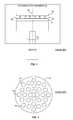
- FIG. 1is an illustration of a CVD reaction chamber as is known in the art.
- FIG. 2is an illustration of the wafer carrier of FIG. 1 .
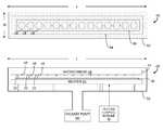
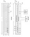
- FIG. 3A and FIG. 3Bshow a top view and a side view, respectively, of one embodiment of a linear batch CVD system according to the invention.
- FIG. 4Ashows a cross-sectional view through one of the receptacles of the substrate carrier of FIG. 3A and FIG. 3B .
- FIG. 4Bshows a cross-sectional view of an alternative substrate carrier according to another embodiment of the invention.
- FIG. 4Cis a top view of the substrate carrier of FIG. 4B showing rotation of the wafers about a substrate axis.
- FIG. 5is a cross-sectional view through a wafer and substrate carrier showing a side view of two injector ports arranged in a perpendicular configuration according to one embodiment of the invention.
- FIG. 6shows a top view of an arrangement of injector ports according to one embodiment of the invention.
- FIG. 7shows a top view of an arrangement of injector ports according to another embodiment of the invention.
- FIG. 8A , FIG. 8B and FIG. 8Cshow top views of an arrangement of injector ports at various positions according to another embodiment of the invention.
- FIG. 9shows a configuration of injector ports according to another embodiment of the invention.
- FIG. 10shows a top view of injector nozzles according to one embodiment of the invention.
- the steps of the methods of the present inventioncan be performed in any order with operable results and two or more steps can be performed simultaneously unless otherwise noted.
- the systems and methods of the present inventionmay include any of the described embodiments or combinations of the described embodiments in an operable manner.
- the present teachingrelates to systems and methods for reactive gas phase processing such as CVD, MOCVD and Halide Vapor Phase Epitaxy (HVPE) processes.
- reactive gas phase processingsuch as CVD, MOCVD and Halide Vapor Phase Epitaxy (HVPE) processes.
- semiconductor wafersare mounted in a carrier inside a reaction chamber.
- a gas distribution injectoris configured to face the carrier.
- the injectortypically includes gas inlets that receive a plurality of gases or combinations of gases.
- the injectordirects the gases or combination of gases to the reaction chamber.
- Injectorscommonly include showerhead devices arranged in a pattern that enables the precursor gases to react as close to each wafer surface as possible to maximize the efficiency of the reaction processes and epitaxial growth at the surface.
- Some gas distribution injectorsinclude a shroud to assist in providing a laminar gas flow during the CVD process.
- One or more carrier gasescan be used to assist in generating and maintaining the laminar gas flow.
- the carrier gasesdo not react with the precursor gases and do not otherwise affect the CVD process.
- a typical gas distribution injectordirects the precursor gases from the gas inlets to targeted regions of the reaction chamber where the wafers are processed.
- the gas distribution injectorintroduces combinations of precursor gases including metal organics and hydrides into the reaction chamber.
- a carrier gassuch as hydrogen or nitrogen, or an inert gas such as argon or helium, is introduced into the chamber through the injector to help sustain a laminar flow at the wafers.
- the precursor gasesmix and react within the chamber to form a film on the wafers.
- the wafersare typically maintained at an elevated temperature and the precursor gases are typically maintained at a lower temperature when introduced into the reaction chamber.
- the temperature of the precursor gases and thus their available energy for reactionincreases as the gases flow past the hotter wafers.
- FIG. 1One common type of CVD reaction chamber 10 is shown in FIG. 1 .
- the chamber 10includes a disc shaped wafer carrier 14 shown in an unpopulated state in more detail in FIG. 2 .
- the carrier 14has pockets 18 or other structural features arranged to hold one or more wafers 22 on a top surface.
- the carrier 14rotates about a vertical axis (dashed line 26 ) that extends perpendicular to the wafer-bearing surface and each wafer 22 is rotated about a wafer axis that is centered on and perpendicular to the wafer surface to achieve planetary motion. Rotation of the carrier 14 and wafers 22 improves the uniformity of the deposited material.
- the precursor gasesare introduced into the reaction chamber 10 from a flow inlet element 30 above the carrier 14 .
- the flowing gasespass downward toward the wafers 22 , preferably in a laminar plug flow.
- viscous dragimpels the gases into rotation about the axis 26 . Consequently, in a boundary region near the carrier surface and wafers 22 , the gases flow around the axis 26 and outward toward the edge of the carrier 14 .
- the gasesflow past the carrier edge and then downward toward one or more exhaust ports.
- MOCVD processare performed using a succession of different precursor gases and, in some instances, different wafer temperatures, to deposit a plurality of different layers each having a different composition to form a device.
- CVD processesare typically limited in batch capacity. For example, achieving uniformity of the deposited film for all substrates in a conventional CVD reaction chamber (e.g., chamber 10 in FIG. 1 ) is generally difficult, especially as the size of the reaction chamber increases to allow for more substrates to be processed or to accommodate larger substrates. Conventional systems and methods for CVD processing are often inadequate to support high volume processing of wafers and other substrates without sacrificing uniformity of the deposited films or requiring redundant equipment.
- the systems and methods of the present inventionare suitable for high volume batch CVD processing of substrates.
- the narrow width of the reaction chamber of the systemsenables a uniform distribution of the precursor gases across the substrates along the entire length of the chamber.
- the number of substrates that can be coated with uniform film thickness and composition during a single CVD process runis scalable and can be substantially larger than the number of substrates processed in a typical CVD reaction chamber. Moreover, complicated motion mechanisms are not required and each substrate is simply rotated about a single substrate axis.
- FIG. 3A and FIG. 3Bare top and side views, respectively, of an embodiment of a linear batch CVD system 40 according to the present invention.
- the top down viewis from underneath a shower head 44 structure that includes gas injectors 48 as shown in FIG. 3B .
- the linear batch CVD system 40includes a deposition chamber 52 , substrate carrier 56 , vacuum system 60 , the shower head 44 and a heating system that includes a heater 64 and a heating control module 68 .
- the substrate carrier 56includes a plurality of receptacles 72 each configured to receive a substrate 22 .
- the substrate 22is generally described as a wafer, such as a semiconductor wafer; however, it should be recognized that other forms and types of substrates can be used.
- the width W of the deposition chamber 52is substantially narrower than the length L and accommodates only a single row of wafers 22 .
- the rowis shown as a straight line, the invention contemplates other types of rows in which the wafers 22 are arranged in a curved line or other shape so that the dimension perpendicular to the row at any location is substantially less than the length of the row.
- the linear configurationcan include a batch of wafers 22 arranged along a straight line, a curved line, or any combination of straight line segments and curved line segments.
- the narrow dimension of the configurationenables a uniform distribution of precursor gases across all the wafers 22 in the batch.
- wafers 22are loaded into respective receptacles 72 in the substrate carrier 56 .
- Loadingis preferably performed in an automated manner, for example, by retrieving the wafers 22 from a wafer supply and positioning each wafer 22 into its receptacle 72 using one or more robotic mechanisms disposed near one side of the deposition chamber 52 .
- processed wafers 22can be removed from the receptacles using robotic means.
- FIG. 4Ais a cross-sectional view of the substrate carrier 56 through one of the receptacles 72 .
- Each receptacle 72includes a recessed region to maintain the position of the wafers 22 within the carrier 56 .
- the wafer 22is disposed on an intermediate substrate carrier 76 that resides in the receptacle 72 .
- the heater 64includes a plurality of heating elements 80 positioned near the bottom of the substrate carrier 56 and arranged substantially parallel to the length of the carrier 56 .
- the heating elements 80may be wires or filament heaters that generate heat while conducting an electrical current.
- the heating elements 80may be lamp heaters or RF heaters.
- Heatis coupled from the heating elements 80 to the substrate carrier 56 via radiative coupling.
- the substrate carrier 56comprises graphite or another material having a high thermal conductivity to efficiently conduct heat to the wafers 22 .
- the heating elements 80are independently controlled, or are controlled as subsets of the total number of elements. Individual element control or group control allows temperature variations due to radiation loss from the sides of the substrate carrier 56 to be compensated by applying greater heat near the sides of the carrier 56 .
- the heating elements 80do not extend the length of the carrier 56 , but are instead arranged in zones of shorter lengths that together span nearly the full length of the deposition chamber. The shorter heating zones may be independently controlled in response to temperature measurements at different locations along the length of the deposition chamber to achieve a more uniform temperature environment.
- FIG. 4Billustrates a cross-sectional view of a substrate carrier 56 ′ according to another embodiment.
- Each receptacle 72 in the substrate carrier 56 ′has a plurality of air injector channels 84 that, when active, allow gas to flow upward to provide an air bearing support that floats the intermediate substrate carrier 76 and wafer 22 .
- At least some of the air injector channels 84 in each receptacle 72are configured at a non-zero angle with respect to the vertical axis 88 to impart a rotation to the intermediate substrate carrier 76 about the vertical axis 88 so that each intermediate carrier 76 and wafer 22 rotate as shown in FIG. 4C .
- the CVD system 40includes one or more sensors to sense the temperature across the wafers. Temperature sensors communicate with the heating control module 68 to enable more accurate control of the wafer temperatures.
- the temperature sensorcan be a pyrometer or other sensor adapted for determining the high temperatures of the wafers 22 during the CVD process.
- one or more thermocouples disposed on the substrate carrier 56communicate with the heating control module 68 to provide a feedback signal to enable accurate control of the wafer temperatures.
- the CVD system 40includes one or more film thickness sensors to determine the thickness of the films being deposited on the wafers 22 .
- the film thickness sensorcan be an optical reflectometer or similar measurement system as known in the art.
- a temperature sensor and film thickness sensorcan be integrated in a single measurement head used to monitor conditions during a CVD process.
- a plurality of measurement headsare positioned along the length L of the deposition chamber 52 to obtain temperature and thickness data for a subset of the total number of wafers 22 , for example, the measurement heads can be positioned to obtain data for every third wafer 22 in the linear configuration.
- a single measurement head having a temperature sensor and a film thickness sensoris mounted to a translation mechanism, such as a linear drive, that enables the measurement head to be moved along the length L of the deposition chamber 52 .
- a window above each wafer 22enables the moving head to obtain data for each wafer 22 .
- the wafer measurementsare used to control the heater 64 and the precursor gas flows.
- the showerhead 44provides a uniform distribution of the precursor gases at the surface of each wafer 22 .
- the showerhead 44includes one or more gas injectors for each precursor gas.
- the precursor gases in a two precursor gas implementationcan include trimethylgallium (TMG) and ammonia gases used in the production of gallium nitride (GaN) light-emitting diodes (LEDs).
- the precursor gasesit is preferable to sequentially activate, or pulse, the precursor gases so that substantially only one gas is present in the deposition chamber 52 . Pulsing of the precursor gases in this manner limits the mixing of the gases in the chamber and reduces or eliminates parasitic deposition.
- One slot 92 Aprovides a precursor gas (gas “A”) in a horizontal flow that is substantially parallel to the wafer surface.
- the other slot 92 Bprovides a different precursor gas (gas “B”) in a vertical flow that is substantially parallel to the axis 88 of the wafer 22 .
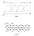
- FIG. 6shows a top view of an arrangement of injector ports 92 with respect to four adjacent substrates 22 according to another embodiment.
- Each injector port 92is in the form of a slot, or substantially rectangular opening, and has a length L SLOT that extends parallel to the length L of the deposition chamber 52 (see FIG. 3A ).
- the width W SLOTS of the full arrangement of slots 92is greater than the diameter of the substrates 22 .
- Precursor gas Ais supplied from slots 92 A that are spaced in alternating arrangement with slots 92 B that supply precursor gas B.
- the lengths L SLOT of the slots 92are nearly as long as the length of the deposition chamber.
- the slots 92are configured in two or more groups so that the lengths L SLOT of the slots 92 in a group is substantially less than the length of the deposition chamber.
- Injector port groupingis preferable in some configurations having a high batch capacity to enable more uniform precursor gas distribution across the narrow dimension of the deposition chamber.
- the lengths L SLOT of slots in a groupcan be one meter for a deposition chamber that is several meters in length.
- the spacing between adjacent wafers 22 in neighboring groupsmay exceed the spacing between wafers 22 within the same port group.
- the precursor gas flows for each groupcan be independently controlled to enable more uniform deposition of films for the full batch of wafers 22 in the deposition chamber.
- FIG. 7shows a top view of an alternative embodiment to the slots 92 illustrated in FIG. 6 .
- Each slot 92has a length L SLOT that extends parallel to the shorter dimension (i.e., the width W shown in FIG. 3A ) of the deposition chamber and is greater than the diameters of the wafers 22 .
- the slots 92 A and 92 Bare arranged in alternating position along the length of the deposition chamber. In one embodiment, the full width W SLOTS of the configuration of slots 92 is nearly the length of the deposition chamber.
- the slots 92are arranged in groups each having a group width that is substantially less than the length of the deposition chamber.
- the spacing between adjacent wafers 22 belonging to neighboring slot groupscan exceed the spacing between wafers 22 within a slot group.
- the gas flow for injector ports in the slot groupscan be independently controlled to improve the uniformity of film deposition for all wafers 22 in the deposition chamber.
- FIG. 8Ashows an alternative configuration in which a single pair of injector ports (i.e., a “port pair”) includes one slot 92 A to supply precursor gas A and a second slot 92 B to supply precursor gas B.
- the port pairis swept in a back and forth motion above the wafers 22 using a translation mechanism such as a single-axis translation stage. For example, the port pair moves from one side of the row of wafers 22 as shown in FIG. 8A , through intermediate positions (for example, as shown in one intermediate position in FIG.
- FIG. 9shows a configuration of gas injectors according to another embodiment in which one slot 92 A that supplies precursor gas A is on an opposite side of the row of wafers 22 from another slot 92 B that supplies precursor gas B.
- first slot 92 Amoves from the illustrated position across the row of wafers 22 until it is adjacent to the second slot 92 B.
- the first slot 92 Athen translates in a reverse direction until it returns to the illustrated position.
- the second slot 92 Bremains stationary when the first slot 92 A is in motion.
- the second slot 92 Bis moved from its illustrated position across the row of wafers 22 until it is adjacent to the first slot 92 A.
- the second slot 92 Bthen reverses direction and moves across the wafers 22 until it reaches its illustrated position.
- the first slot 92 Aremains stationary while the second slot is in motion.
- This alternating motion in which the first slot 92 A moves and then the second slot 92 B movesis repeated throughout the CVD process.
- the two precursor gases supplied by the slots 92are sequentially pulsed so that gas is supplied from a slot only when the slot is in motion so that parasitic deposition is substantially reduced.
- one slot 92may begin its motion before the other slot 92 completes its motion as long as the slots do not interfere with each other.
- the gas injectorsinclude ports 92 that are substantially rectangular or slotted; however, other forms of gas injectors are contemplated.
- the gas injectorscan be in the form of injector tubes uniformly distributed over the substrate carrier 56 .
- Portscan be any of a variety of openings such as holes or various shaped apertures through a sidewall of the tube facing the substrate carrier 56 .
- FIG. 10is a top view relating to another embodiment and shows a configuration of injector nozzles 96 with respect to four adjacent wafers 22 .
- the number of nozzles 96 above each wafer 22may be different and only nine nozzles are shown with each wafer 22 for clarity.
- Some nozzles 96 Asupply a first precursor gas (e.g., gas A) and the other nozzles 96 B supply a second precursor gas (e.g., gas B) so that a substantially uniform distribution of each gas is present near and at the surface of each wafer 22 .
- the nozzles 96are controlled in subsets, or groups, defined for zones for subsets of the total number of wafers 22 arranged along the length of the deposition chamber.
Landscapes
- Chemical & Material Sciences (AREA)
- Engineering & Computer Science (AREA)
- General Chemical & Material Sciences (AREA)
- Chemical Kinetics & Catalysis (AREA)
- Materials Engineering (AREA)
- Mechanical Engineering (AREA)
- Metallurgy (AREA)
- Organic Chemistry (AREA)
- Physics & Mathematics (AREA)
- Condensed Matter Physics & Semiconductors (AREA)
- General Physics & Mathematics (AREA)
- Manufacturing & Machinery (AREA)
- Computer Hardware Design (AREA)
- Microelectronics & Electronic Packaging (AREA)
- Power Engineering (AREA)
- Chemical Vapour Deposition (AREA)
Abstract
Description
Claims (19)
Priority Applications (7)
| Application Number | Priority Date | Filing Date | Title |
|---|---|---|---|
| US12/787,082US8986451B2 (en) | 2010-05-25 | 2010-05-25 | Linear batch chemical vapor deposition system |
| KR1020157018457AKR20150085137A (en) | 2010-05-25 | 2011-05-12 | Linear batch chemical vapor deposition system |
| CN201180033855.9ACN102985592B (en) | 2010-05-25 | 2011-05-12 | Linear batch chemical vapor deposition system |
| KR1020127033164AKR20130055623A (en) | 2010-05-25 | 2011-05-12 | Linear batch chemical vapor deposition system |
| PCT/US2011/036167WO2011149678A2 (en) | 2010-05-25 | 2011-05-12 | Linear batch chemical vapor deposition system |
| US13/469,515US9169562B2 (en) | 2010-05-25 | 2012-05-11 | Parallel batch chemical vapor deposition system |
| US13/900,028US9869021B2 (en) | 2010-05-25 | 2013-05-22 | Showerhead apparatus for a linear batch chemical vapor deposition system |
Applications Claiming Priority (1)
| Application Number | Priority Date | Filing Date | Title |
|---|---|---|---|
| US12/787,082US8986451B2 (en) | 2010-05-25 | 2010-05-25 | Linear batch chemical vapor deposition system |
Related Child Applications (2)
| Application Number | Title | Priority Date | Filing Date |
|---|---|---|---|
| US13/469,515Continuation-In-PartUS9169562B2 (en) | 2010-05-25 | 2012-05-11 | Parallel batch chemical vapor deposition system |
| US13/900,028Continuation-In-PartUS9869021B2 (en) | 2010-05-25 | 2013-05-22 | Showerhead apparatus for a linear batch chemical vapor deposition system |
Publications (2)
| Publication Number | Publication Date |
|---|---|
| US20110293831A1 US20110293831A1 (en) | 2011-12-01 |
| US8986451B2true US8986451B2 (en) | 2015-03-24 |
Family
ID=45004655
Family Applications (1)
| Application Number | Title | Priority Date | Filing Date |
|---|---|---|---|
| US12/787,082Expired - Fee RelatedUS8986451B2 (en) | 2010-05-25 | 2010-05-25 | Linear batch chemical vapor deposition system |
Country Status (4)
| Country | Link |
|---|---|
| US (1) | US8986451B2 (en) |
| KR (2) | KR20130055623A (en) |
| CN (1) | CN102985592B (en) |
| WO (1) | WO2011149678A2 (en) |
Families Citing this family (12)
| Publication number | Priority date | Publication date | Assignee | Title |
|---|---|---|---|---|
| KR101685150B1 (en)* | 2011-01-14 | 2016-12-09 | 주식회사 원익아이피에스 | Thin film deposition apparatus and substrate processing system comprising the same |
| US20130171350A1 (en)* | 2011-12-29 | 2013-07-04 | Intermolecular Inc. | High Throughput Processing Using Metal Organic Chemical Vapor Deposition |
| CN102534567B (en)* | 2012-03-21 | 2014-01-15 | 中微半导体设备(上海)有限公司 | Device and method for controlling basal heating in chemical gaseous phase sedimentary chamber |
| KR101881894B1 (en)* | 2012-04-06 | 2018-07-26 | 삼성디스플레이 주식회사 | Thin film depositing apparatus and the thin film depositing method using the same |
| DE102012104475A1 (en) | 2012-05-24 | 2013-11-28 | Aixtron Se | Device useful for depositing layer on substrate comprises processing chamber having susceptor heated by heating device for receiving substrate, gas inlet element, gas outlet element and gas-tight reactor housing which is outwardly arranged |
| US20130323422A1 (en)* | 2012-05-29 | 2013-12-05 | Applied Materials, Inc. | Apparatus for CVD and ALD with an Elongate Nozzle and Methods Of Use |
| CN103022260B (en)* | 2012-12-28 | 2015-07-08 | 英利能源(中国)有限公司 | Method for adjusting thicknesses and refractive indexes of antireflection films |
| US9232569B2 (en)* | 2013-02-27 | 2016-01-05 | Applied Materials, Inc. | Solid state light source assisted processing |
| US9373551B2 (en)* | 2013-03-12 | 2016-06-21 | Taiwan Semiconductor Manufacturing Co., Ltd. | Moveable and adjustable gas injectors for an etching chamber |
| EP3184666B1 (en)* | 2015-12-23 | 2018-06-13 | Singulus Technologies AG | System and method for gas phase deposition |
| US11261538B1 (en)* | 2020-09-21 | 2022-03-01 | Applied Materials, Inc. | In-situ temperature mapping for epi chamber |
| CN114855271B (en)* | 2022-04-22 | 2024-10-11 | 浙江晶盛光子科技有限公司 | Epitaxial growth device |
Citations (33)
| Publication number | Priority date | Publication date | Assignee | Title |
|---|---|---|---|---|
| US3602192A (en)* | 1969-05-19 | 1971-08-31 | Ibm | Semiconductor wafer processing |
| US3805736A (en)* | 1971-12-27 | 1974-04-23 | Ibm | Apparatus for diffusion limited mass transport |
| US4262131A (en)* | 1979-04-02 | 1981-04-14 | The Upjohn Company | 19-Hydroxy-inter-phenylene-PG1 componds |
| US4579080A (en)* | 1983-12-09 | 1986-04-01 | Applied Materials, Inc. | Induction heated reactor system for chemical vapor deposition |
| US4823736A (en)* | 1985-07-22 | 1989-04-25 | Air Products And Chemicals, Inc. | Barrel structure for semiconductor epitaxial reactor |
| US5119760A (en)* | 1988-12-27 | 1992-06-09 | Symetrix Corporation | Methods and apparatus for material deposition |
| US5366554A (en)* | 1986-01-14 | 1994-11-22 | Canon Kabushiki Kaisha | Device for forming a deposited film |
| JPH1050613A (en) | 1996-07-30 | 1998-02-20 | Sony Corp | Epitaxial growth device |
| US5788777A (en)* | 1997-03-06 | 1998-08-04 | Burk, Jr.; Albert A. | Susceptor for an epitaxial growth factor |
| US5958140A (en) | 1995-07-27 | 1999-09-28 | Tokyo Electron Limited | One-by-one type heat-processing apparatus |
| US6197121B1 (en)* | 1996-11-27 | 2001-03-06 | Emcore Corporation | Chemical vapor deposition apparatus |
| US20020033133A1 (en)* | 2000-07-27 | 2002-03-21 | Klein Martin P. | Substrate processing pallet and related substrate processing method and machine |
| US20020069827A1 (en) | 2000-09-20 | 2002-06-13 | Kiyotoshi Sakamoto | Film formation apparatus |
| US6416579B1 (en) | 1999-01-13 | 2002-07-09 | Erich Thallner | Apparatus for treating silicon wafers |
| US20030061989A1 (en)* | 2001-08-31 | 2003-04-03 | Kabushiki Kaisha Toshiba | Semiconductor manufacturing system |
| US20030072882A1 (en) | 2001-08-03 | 2003-04-17 | Jaakko Niinisto | Method of depositing rare earth oxide thin films |
| US20040067641A1 (en)* | 2002-10-02 | 2004-04-08 | Applied Materials, Inc. | Gas distribution system for cyclical layer deposition |
| KR20040046042A (en) | 2002-11-26 | 2004-06-05 | (주) 윈테크 | structure of boat and process tube of the axial type heat-treatment for performing atomic layer deposition |
| US6843892B1 (en)* | 2002-02-19 | 2005-01-18 | Seagate Technology Llc | Apparatus and method for selectively and controllably electrically biasing a plurality of substrates on a pallet |
| US6886244B1 (en)* | 2002-02-25 | 2005-05-03 | Seagate Technology Llc | Segmented pallet for disk-shaped substrate electrical biassing and apparatus comprising same |
| US7041202B2 (en)* | 2002-08-02 | 2006-05-09 | Seagate Technology Llc | Timing apparatus and method to selectively bias during sputtering |
| US20060126701A1 (en) | 2002-10-30 | 2006-06-15 | Matsushita Electric Industrial Co., Ltd. | Method of estimating substrate temperature |
| US20060144335A1 (en)* | 2004-12-30 | 2006-07-06 | Research Electro-Optics, Inc. | Methods and devices for monitoring and controlling thin film processing |
| US7153368B2 (en)* | 2001-09-07 | 2006-12-26 | Lpe Spa | Susceptor with epitaxial growth control devices and epitaxial reactor using the same |
| US20070077355A1 (en) | 2005-09-30 | 2007-04-05 | Applied Materials, Inc. | Film formation apparatus and methods including temperature and emissivity/pattern compensation |
| US20080213477A1 (en) | 2007-03-02 | 2008-09-04 | Arno Zindel | Inline vacuum processing apparatus and method for processing substrates therein |
| US20080251020A1 (en)* | 2005-11-19 | 2008-10-16 | Walter Franken | Cvd-Reactor with Slidingly Mounted Susceptor Holder |
| US20090017190A1 (en) | 2007-07-10 | 2009-01-15 | Veeco Instruments Inc. | Movable injectors in rotating disc gas reactors |
| US20090042394A1 (en)* | 2003-02-05 | 2009-02-12 | Semiconductor Energy Laboratory Co., Ltd. | Manufacturing method for wiring |
| US20090098276A1 (en)* | 2007-10-16 | 2009-04-16 | Applied Materials, Inc. | Multi-gas straight channel showerhead |
| US20120219713A1 (en)* | 2010-05-25 | 2012-08-30 | Aventa Technologies, Llc | Parallel batch chemical vapor deposition system |
| US8303713B2 (en) | 2008-12-04 | 2012-11-06 | Veeco Instruments Inc. | Chemical vapor deposition flow inlet elements and methods |
| US20130270362A1 (en)* | 2010-05-25 | 2013-10-17 | Aventa Technologies, Inc. | Showerhead apparatus for a linear batch chemical vapor deposition system |
- 2010
- 2010-05-25USUS12/787,082patent/US8986451B2/ennot_activeExpired - Fee Related
- 2011
- 2011-05-12KRKR1020127033164Apatent/KR20130055623A/ennot_activeCeased
- 2011-05-12CNCN201180033855.9Apatent/CN102985592B/ennot_activeExpired - Fee Related
- 2011-05-12WOPCT/US2011/036167patent/WO2011149678A2/enactiveApplication Filing
- 2011-05-12KRKR1020157018457Apatent/KR20150085137A/ennot_activeWithdrawn
Patent Citations (34)
| Publication number | Priority date | Publication date | Assignee | Title |
|---|---|---|---|---|
| US3602192A (en)* | 1969-05-19 | 1971-08-31 | Ibm | Semiconductor wafer processing |
| US3805736A (en)* | 1971-12-27 | 1974-04-23 | Ibm | Apparatus for diffusion limited mass transport |
| US4262131A (en)* | 1979-04-02 | 1981-04-14 | The Upjohn Company | 19-Hydroxy-inter-phenylene-PG1 componds |
| US4579080A (en)* | 1983-12-09 | 1986-04-01 | Applied Materials, Inc. | Induction heated reactor system for chemical vapor deposition |
| US4823736A (en)* | 1985-07-22 | 1989-04-25 | Air Products And Chemicals, Inc. | Barrel structure for semiconductor epitaxial reactor |
| US5366554A (en)* | 1986-01-14 | 1994-11-22 | Canon Kabushiki Kaisha | Device for forming a deposited film |
| US5119760A (en)* | 1988-12-27 | 1992-06-09 | Symetrix Corporation | Methods and apparatus for material deposition |
| US5958140A (en) | 1995-07-27 | 1999-09-28 | Tokyo Electron Limited | One-by-one type heat-processing apparatus |
| JPH1050613A (en) | 1996-07-30 | 1998-02-20 | Sony Corp | Epitaxial growth device |
| US6197121B1 (en)* | 1996-11-27 | 2001-03-06 | Emcore Corporation | Chemical vapor deposition apparatus |
| US5788777A (en)* | 1997-03-06 | 1998-08-04 | Burk, Jr.; Albert A. | Susceptor for an epitaxial growth factor |
| US6416579B1 (en) | 1999-01-13 | 2002-07-09 | Erich Thallner | Apparatus for treating silicon wafers |
| US20020033133A1 (en)* | 2000-07-27 | 2002-03-21 | Klein Martin P. | Substrate processing pallet and related substrate processing method and machine |
| US6578515B2 (en)* | 2000-09-20 | 2003-06-17 | Fuji Daiichi Seisakusho Co., Ltd. | Film formation apparatus comprising movable gas introduction members |
| US20020069827A1 (en) | 2000-09-20 | 2002-06-13 | Kiyotoshi Sakamoto | Film formation apparatus |
| US20030072882A1 (en) | 2001-08-03 | 2003-04-17 | Jaakko Niinisto | Method of depositing rare earth oxide thin films |
| US20030061989A1 (en)* | 2001-08-31 | 2003-04-03 | Kabushiki Kaisha Toshiba | Semiconductor manufacturing system |
| US7153368B2 (en)* | 2001-09-07 | 2006-12-26 | Lpe Spa | Susceptor with epitaxial growth control devices and epitaxial reactor using the same |
| US6843892B1 (en)* | 2002-02-19 | 2005-01-18 | Seagate Technology Llc | Apparatus and method for selectively and controllably electrically biasing a plurality of substrates on a pallet |
| US6886244B1 (en)* | 2002-02-25 | 2005-05-03 | Seagate Technology Llc | Segmented pallet for disk-shaped substrate electrical biassing and apparatus comprising same |
| US7041202B2 (en)* | 2002-08-02 | 2006-05-09 | Seagate Technology Llc | Timing apparatus and method to selectively bias during sputtering |
| US20040067641A1 (en)* | 2002-10-02 | 2004-04-08 | Applied Materials, Inc. | Gas distribution system for cyclical layer deposition |
| US20060126701A1 (en) | 2002-10-30 | 2006-06-15 | Matsushita Electric Industrial Co., Ltd. | Method of estimating substrate temperature |
| KR20040046042A (en) | 2002-11-26 | 2004-06-05 | (주) 윈테크 | structure of boat and process tube of the axial type heat-treatment for performing atomic layer deposition |
| US20090042394A1 (en)* | 2003-02-05 | 2009-02-12 | Semiconductor Energy Laboratory Co., Ltd. | Manufacturing method for wiring |
| US20060144335A1 (en)* | 2004-12-30 | 2006-07-06 | Research Electro-Optics, Inc. | Methods and devices for monitoring and controlling thin film processing |
| US20070077355A1 (en) | 2005-09-30 | 2007-04-05 | Applied Materials, Inc. | Film formation apparatus and methods including temperature and emissivity/pattern compensation |
| US20080251020A1 (en)* | 2005-11-19 | 2008-10-16 | Walter Franken | Cvd-Reactor with Slidingly Mounted Susceptor Holder |
| US20080213477A1 (en) | 2007-03-02 | 2008-09-04 | Arno Zindel | Inline vacuum processing apparatus and method for processing substrates therein |
| US20090017190A1 (en) | 2007-07-10 | 2009-01-15 | Veeco Instruments Inc. | Movable injectors in rotating disc gas reactors |
| US20090098276A1 (en)* | 2007-10-16 | 2009-04-16 | Applied Materials, Inc. | Multi-gas straight channel showerhead |
| US8303713B2 (en) | 2008-12-04 | 2012-11-06 | Veeco Instruments Inc. | Chemical vapor deposition flow inlet elements and methods |
| US20120219713A1 (en)* | 2010-05-25 | 2012-08-30 | Aventa Technologies, Llc | Parallel batch chemical vapor deposition system |
| US20130270362A1 (en)* | 2010-05-25 | 2013-10-17 | Aventa Technologies, Inc. | Showerhead apparatus for a linear batch chemical vapor deposition system |
Non-Patent Citations (6)
| Title |
|---|
| First Office Action in Chinese patent application No. 201180033855.9, issued on Apr. 1, 2014; 19 pages. |
| First Office Action in related Korean Patent Application No. 10-2012-7033164, mailed on Oct. 6, 2014; 16 pages. |
| International Search Report & Written Opinion in related international patent application No. PCT/US14/35812, mailed on Sep. 5, 2014; 7 pages. |
| International Search Report and Written Opinion in counterpart international patent application No. PCT/US2011/036167 dated Jan. 9, 2012; 10 pages. |
| Second Office Action in related Chinese Patent Application No. 201180033855.9, mailed on Nov. 19, 2014; 8 pages. |
| Sferlazzo, Piero et al.; "Web Substrate Deposition System"; U.S. Appl. No. 12/466,221, filed May 14, 2009. |
Also Published As
| Publication number | Publication date |
|---|---|
| WO2011149678A2 (en) | 2011-12-01 |
| CN102985592A (en) | 2013-03-20 |
| WO2011149678A3 (en) | 2012-04-19 |
| US20110293831A1 (en) | 2011-12-01 |
| KR20130055623A (en) | 2013-05-28 |
| KR20150085137A (en) | 2015-07-22 |
| CN102985592B (en) | 2015-05-06 |
Similar Documents
| Publication | Publication Date | Title |
|---|---|---|
| US8986451B2 (en) | Linear batch chemical vapor deposition system | |
| US9869021B2 (en) | Showerhead apparatus for a linear batch chemical vapor deposition system | |
| US9175392B2 (en) | System for multi-region processing | |
| US9556522B2 (en) | High throughput multi-wafer epitaxial reactor | |
| US8673081B2 (en) | High throughput multi-wafer epitaxial reactor | |
| US10900125B2 (en) | Apparatus for susceptor temperature verification and methods of use | |
| US20160160387A1 (en) | Linear Cluster Deposition System | |
| US20110290175A1 (en) | Multi-Chamber CVD Processing System | |
| KR20140084308A (en) | Gas dispersion apparatus | |
| KR20080081823A (en) | Microbatch Deposition Chambers with Radiant Heating | |
| KR20160013158A (en) | A coated liner assembly for a semiconductor processing chamber | |
| US9169562B2 (en) | Parallel batch chemical vapor deposition system | |
| US20140318442A1 (en) | High throughput epitaxial deposition system for single crystal solar devices | |
| US20110262641A1 (en) | Inline chemical vapor deposition system | |
| WO2012120991A1 (en) | Substrate processing apparatus and method for manufacturing substrate | |
| KR100991978B1 (en) | Reactor for chemical vapor deposition | |
| KR101716355B1 (en) | Apparatus and Method for treating substrate | |
| US20160027674A1 (en) | Carousel Gas Distribution Assembly With Optical Measurements | |
| TWI490367B (en) | Mocvd (metal organic chemical vapor deposition) method and apparatus thereof | |
| WO2014189650A1 (en) | Showerhead apparatus for a linear batch chemical vapor deposition system | |
| KR102797993B1 (en) | Apparatus for heating wafer | |
| KR101297344B1 (en) | A chemical vapor deposition apparatus and a gas supply unit thereof |
Legal Events
| Date | Code | Title | Description |
|---|---|---|---|
| AS | Assignment | Owner name:AVENTA SYSTEMS, LLC, MASSACHUSETTS Free format text:ASSIGNMENT OF ASSIGNORS INTEREST;ASSIGNOR:SFERLAZZO, PIERO;REEL/FRAME:024845/0704 Effective date:20100804 | |
| AS | Assignment | Owner name:AVENTA TECHNOLOGIES, INC., MASSACHUSETTS Free format text:MERGER;ASSIGNOR:AVENTA SYSTEMS, LLC;REEL/FRAME:029034/0406 Effective date:20120824 | |
| AS | Assignment | Owner name:RICHARD S. POST, MASSACHUSETTS Free format text:SECURITY AGREEMENT;ASSIGNOR:AVENTA TECHNOLOGIES, INC.;REEL/FRAME:030628/0796 Effective date:20130606 | |
| AS | Assignment | Owner name:AVENTA TECHNOLOGIES, INC., MASSACHUSETTS Free format text:RELEASE BY SECURED PARTY;ASSIGNOR:POST, RICHARD S.;REEL/FRAME:031530/0398 Effective date:20131029 | |
| AS | Assignment | Owner name:SINGULUS MOCVD GMBH I.GR., GERMANY Free format text:ASSIGNMENT OF ASSIGNORS INTEREST;ASSIGNOR:AVENTA TECHNOLOGIES, INC.;REEL/FRAME:031536/0298 Effective date:20131029 | |
| AS | Assignment | Owner name:AVENTA TECHNOLOGIES, INC., MASSACHUSETTS Free format text:SECURITY AGREEMENT;ASSIGNOR:SINGULUS MOCVD GMBH I.GR.;REEL/FRAME:031581/0712 Effective date:20131029 | |
| STCF | Information on status: patent grant | Free format text:PATENTED CASE | |
| FEPP | Fee payment procedure | Free format text:ENTITY STATUS SET TO SMALL (ORIGINAL EVENT CODE: SMAL) | |
| MAFP | Maintenance fee payment | Free format text:PAYMENT OF MAINTENANCE FEE, 4TH YR, SMALL ENTITY (ORIGINAL EVENT CODE: M2551) Year of fee payment:4 | |
| FEPP | Fee payment procedure | Free format text:MAINTENANCE FEE REMINDER MAILED (ORIGINAL EVENT CODE: REM.); ENTITY STATUS OF PATENT OWNER: SMALL ENTITY | |
| LAPS | Lapse for failure to pay maintenance fees | Free format text:PATENT EXPIRED FOR FAILURE TO PAY MAINTENANCE FEES (ORIGINAL EVENT CODE: EXP.); ENTITY STATUS OF PATENT OWNER: SMALL ENTITY | |
| STCH | Information on status: patent discontinuation | Free format text:PATENT EXPIRED DUE TO NONPAYMENT OF MAINTENANCE FEES UNDER 37 CFR 1.362 | |
| FP | Lapsed due to failure to pay maintenance fee | Effective date:20230324 |