US8983242B2 - Plasmonic device for modulation and amplification of plasmonic signals - Google Patents
Plasmonic device for modulation and amplification of plasmonic signalsDownload PDFInfo
- Publication number
- US8983242B2 US8983242B2US12/023,489US2348908AUS8983242B2US 8983242 B2US8983242 B2US 8983242B2US 2348908 AUS2348908 AUS 2348908AUS 8983242 B2US8983242 B2US 8983242B2
- Authority
- US
- United States
- Prior art keywords
- plasmonic
- beams
- output
- interaction region
- mixer
- Prior art date
- Legal status (The legal status is an assumption and is not a legal conclusion. Google has not performed a legal analysis and makes no representation as to the accuracy of the status listed.)
- Expired - Fee Related, expires
Links
Images


Classifications
- G—PHYSICS
- G02—OPTICS
- G02B—OPTICAL ELEMENTS, SYSTEMS OR APPARATUS
- G02B6/00—Light guides; Structural details of arrangements comprising light guides and other optical elements, e.g. couplings
- G02B6/10—Light guides; Structural details of arrangements comprising light guides and other optical elements, e.g. couplings of the optical waveguide type
- G02B6/12—Light guides; Structural details of arrangements comprising light guides and other optical elements, e.g. couplings of the optical waveguide type of the integrated circuit kind
- G02B6/122—Basic optical elements, e.g. light-guiding paths
- G02B6/1226—Basic optical elements, e.g. light-guiding paths involving surface plasmon interaction
- B—PERFORMING OPERATIONS; TRANSPORTING
- B82—NANOTECHNOLOGY
- B82Y—SPECIFIC USES OR APPLICATIONS OF NANOSTRUCTURES; MEASUREMENT OR ANALYSIS OF NANOSTRUCTURES; MANUFACTURE OR TREATMENT OF NANOSTRUCTURES
- B82Y20/00—Nanooptics, e.g. quantum optics or photonic crystals
Definitions
- the present inventionrelates to communication equipment and, more specifically, to plasmonic circuits.
- SPsSurface plasmons
- SPsalso often referred to as surface-plasmon polaritons
- SPscan be qualitatively viewed as a combination of electromagnetic waves and associated charge waves.
- the electromagnetic wavespropagate along the interface due to their interaction with free surface charges of the metal.
- the interactionalso causes the surface charges to oscillate in resonance with the electromagnetic wave.
- the combined physical entity created via this resonant interactioni.e., an entity including a charge wave and an electromagnetic wave, is an SP.
- a detailed description of certain physical properties of SPscan be found, e.g., in an article by W. L. Barnes, et al., entitled “Surface Plasmon Subwavelength Optics,” published in Nature, 14 Aug. 2003, v. 424, pp. 824-830, the teachings of which are incorporated herein by reference in its entirety.
- SPspropagation is typically characterized by a relatively high rate of attenuation and/or dissipation. More specifically, a beam of SPs propagating along a metal-dielectric interface is attenuated, primarily due to resistive losses in the metal. The rate of attenuation depends on the wavelength and the complex dielectric function of the metal. For example, in the visible spectrum, SP propagation distances along a silver-dielectric interface are in the range between about 10 ⁇ m and about 100 ⁇ m. Jette-Charbonneau et al. (see Optics Express, 2005, v. 13, p. 4674) describe structures/materials, in which SP propagation distances are in the sub-millimeter range.
- a plasmonic devicehas a beam splitter adapted to split a surface-plasmon input beam into first and second split beams and direct them along first and second propagation paths, respectively.
- One of the propagation pathshas a plasmonic-beam interaction region adapted to controllably change the phase accrued by the corresponding split beam within that interaction region in response to a surface-plasmon control signal applied thereto.
- the plasmonic devicefurther has a plasmonic-beam mixer adapted to receive the first and second beams from their respective propagation paths and to mix them to produce a surface-plasmon output signal.
- the plasmonic deviceoperates as a plasmonic-signal amplifier, with the plasmonic output signal providing an amplified version of the plasmonic control signal.
- the plasmonic-signal amplifiercan be used to boost propagation distances for plasmonic signals.
- the plasmonic deviceoperates as a surface-plasmon beam router or a 1 ⁇ 2 surface-plasmon beam switch.
- the plasmonic deviceoperates as a plasmonic modulator, in which one surface-plasmon signal is used to modulate the intensity of another surface-plasmon signal.
- a plasmonic devicehas a first surface plasmon (SP) beam splitter adapted to split an SP input beam into first and second SP beams, to direct the first SP beam along a first propagation path, and to direct the second SP beam along a second propagation path.
- the plasmonic devicealso has a plasmonic-beam interaction region located in the second propagation path and adapted to change a phase of surface plasmons of the second SP beam in a manner responsive to a control signal of surface plasmons applied to said region.
- the plasmonic devicefurther has an SP beam mixer located to receive the first and second SP beams from the first and second propagation paths and to mix said received beams to produce an SP output beam whose amplitude is responsive to said phase.
- a method of processing plasmonic signalscomprises the steps of: (A) splitting an SP input beam into first and second SP beams; (B) directing the first SP beam along a first propagation path; (C) directing the second SP beam along a second propagation path traversing a plasmonic-beam interaction region; (D) applying a control signal of surface plasmons to said interaction region to change a phase of surface plasmons of the second SP beam in said interaction region; and (E) mixing the SP beams from the first and second propagation paths in an SP beam mixer to produce an SP output beam whose amplitude is responsive to said phase.
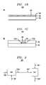
- FIG. 1Ashows a top view of a plasmonic device according to one embodiment of the invention
- FIG. 1Bshows a cross-sectional side view of the plasmonic device of FIG. 1A according to one embodiment of the invention
- FIG. 1Cshows a cross-sectional side view of the plasmonic device of FIG. 1A according to another embodiment of the invention.
- FIG. 2shows a block diagram of a plasmonic device according to another embodiment of the invention.
- FIG. 3shows a top view of a plasmonic device according to yet another embodiment of the invention.
- FIG. 1Ashows a top view of a plasmonic device 100 according to one embodiment of the invention.
- Device 100has a surface-plasmon (SP) beam splitter 110 a that receives a plasmonic input beam 108
- Beam splitter 110 adivides beam 108 into two (attenuated) plasmonic beams 112 a - b and directs them to SP mirrors 120 a - b , respectively.
- SP mirrors 120 a - bthen redirects the corresponding received beam 112 to an SP beam splitter 110 b .
- SPsurface-plasmon
- plasmonic beam 112 bpasses through a plasmonic-beam interaction region 130 , in which the phase of plasmonic beam 112 b can be controllably affected by a plasmonic control signal 128 , which itself is also a plasmonic beam.
- a plasmonic control signal 128which itself is also a plasmonic beam.
- SP beam splitter 110 bacts as a plasmonic-beam mixer that mixes received plasmonic beams 112 a - b to generate two plasmonic output beams 122 a - b.
- the relative phase of plasmonic beams 112 a - b at SP beam splitter 110 bcontrols the intensity of plasmonic output beams 122 a - b .
- intensities I a and I b of plasmonic output beams 122 a - bcan be expressed as follows:
- I aI 0 2 ⁇ ( 1 + sin ⁇ ⁇ ⁇ ) ( 1 ⁇ a )
- I bI 0 2 ⁇ ( 1 - sin ⁇ ⁇ ⁇ ) ( 1 ⁇ b )
- I 0is the intensity of plasmonic input beam 108
- plasmonic beam 122 ais substantially quenched and plasmonic beam 122 b receives substantially all of the output power.
- Intermediate values of ⁇produce intermediate intensities for plasmonic output beams 122 a - b.
- FIG. 1Bshows a cross-sectional side view of plasmonic device 100 according to one embodiment of the invention. More specifically, the view of FIG. 1B shows a cross-section along the plane labeled AA in FIG. 1A , which plane is orthogonal to the plane of that figure.
- Device 100is formed on a substrate 102 .
- a metal layer 104is formed over substrate 102 .
- a dielectric layer 106is formed over metal layer 104 .
- An interface 105 between metal layer 104 and dielectric layer 106serves as a conduit for plasmonic beam 112 a . In other regions of device 100 , interface 105 similarly serves as a conduit for other plasmonic beams.
- dielectric materials for layer 106can be selected, e.g., from a group composed of photoresist materials, silicon, silicon nitride, and silicon oxide. In other embodiments, layer 106 can also be vacuum, air, or another suitable dielectric fluid.
- plasmonic beams 108 , 112 a - b , 122 a - b , and 128are preferably SP beams that remain substantially collimated over propagation distances corresponding to device 100 even in the absence of a special physical structure for laterally confining those beams as they propagate along interface 105 .
- Methods and devices for generating such SP beamsare disclosed, e.g., in (1) D. Egorov, et al., “Two-Dimensional Control of Surface Plasmons and Directional Beaming from Arrays of Subwavelength Apertures,” Phys. Rev. B, 2004, v. 70, pub. 033404 and (2) U.S. Pat. Nos.
- FIG. 1Cshows a cross-sectional side view of plasmonic device 100 according to another embodiment of the invention. Similar to the view of FIG. 1B , the view of FIG. 1C shows a cross-section along plane AA (see FIG. 1A ).
- device 100similarly has substrate 102 , metal layer 104 , and dielectric layer 106 .
- metal layer 104is now patterned to create relatively narrow strips that provide lateral confinement and waveguiding for the corresponding plasmonic beams. For example, edges 103 a - b of patterned metal layer 104 shown in FIG. 1C provide lateral confinement, thereby forming a substantially one-dimensional (1D) waveguide for plasmonic beam 112 a .
- patterned metal layer 104similarly laterally confine and 1D waveguide other plasmonic beams shown in FIG. 1A .
- a 1D plasmonic waveguide created by patterning metal layer 104can have a curved shape that enables that plasmonic waveguide to change the propagation direction of the corresponding plasmonic beam.
- SP mirrors 120 a - bare optional and might not be present in the device structure.
- dielectric layer 106comprises a nonlinear optical material having an optical index of refraction that is a strongly varying function of the electric field (E) applied thereto.
- nonlinear optical materialsinclude, e.g., cuprous oxide, barium titanate, lithium niobate, cadmium zinc telluride, yttrium iron garnet, and zinc telluride.
- other suitable polarizable materials having relatively large dielectric constantse.g., crystalline dielectrics and semiconductors whose unit cells lack inversion or reflection symmetry, can also be used.
- cuprous oxidei.e., cuprous oxide
- the electromagnetic field of plasmonic beam 128affects the effective index of refraction, to which plasmonic beam 112 b is subjected, as described by Eq. (2).
- the phase of plasmonic beam 112 bchanges by amount ⁇ b expressed by Eq. (3):
- ⁇ ⁇ ⁇ ⁇ b4 ⁇ ⁇ ⁇ ⁇ N ⁇ ( E ) ⁇ l ⁇ 0 ( 3 )
- ⁇ 0is the vacuum wavelength
- Eq. (5)assumes that the arms of device 100 have equal lengths.
- those armscan be implemented to have either equal or unequal lengths, e.g., can differ in length by non-integral or integral multiples of the SP wavelength, and that the description of various device configurations below is at least qualitatively applicable to embodiments of device 100 characterized by various relative arms lengths.
- device 100by appropriately selecting two alternate intensity values for plasmonic control signal 128 , the value of ⁇ can be controllably toggled between +90° and ⁇ 90°, thereby changing the propagation direction of the resulting plasmonic output beam.
- device 100operates as a plasmonic-beam router or a 1 ⁇ 2 plasmonic-beam switch.
- device 100can be used to generate a single plasmonic output beam.
- plasmonic beam 122 bcan be blocked, and plasmonic beam 122 a can be used as the single output beam.
- plasmonic beam 122 acan be intensity modulated.
- device 100operates as a plasmonic modulator. Note that, in this modulator, a plasmonic control signal (signal 128 ) is used to modulate the intensity of another plasmonic signal (beam 122 a ).
- the relative phase shift between beams 112 a - b analogous to that represented by the first term in Eq. (5)can be set, e.g., to (m+1 ⁇ 2) ⁇ , where m is an integer.
- the sine functione.g., in Eq. (1b)
- Eq. (6)the sine function
- I b4 ⁇ I 0 ⁇ ( ⁇ ⁇ ⁇ n 2 ⁇ l ⁇ 0 ) 2 ⁇ ⁇ E ⁇ 4 ( 6 )
- plasmonic output beam 122 bbecomes similarly modulated.
- plasmonic input beam 108has a relatively high intensity
- the modulation amplitude of plasmonic beam 122 bwill be greater than the modulation amplitude of plasmonic signal 128 .
- device 100operates as a plasmonic-signal amplifier that amplifies signal 128 .
- plasmonic output beam 122 acan similarly be used as an amplified signal.
- FIG. 2shows a block diagram of a plasmonic device 200 according to another embodiment of the invention.
- Device 200has two cascaded instances of device 100 .
- the upstream and downstream instances of device 100 in device 200 and their corresponding signalsare designated with “prime” and “double-prime” signs, respectively.
- Plasmonic output beam 122 a ′ generated by device 100 ′is launched toward device 100 ′′.
- plasmonic beam 122 a ′propagates between those devices, its intensity diminishes due to resistive losses in metal layer 104 .
- Device 100 ′′then amplifies plasmonic control signal 128 ′′, e.g., as described above, and re-launches it as plasmonic output signal 122 a ′′, thereby advantageously increasing the effective propagation distance for plasmonic signal 122 a ′. If necessary, additional instances of device 100 can be appended downstream of device 100 ′′ to further increase the effective propagation distance for plasmonic signal 122 a′.
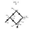
- FIG. 3shows a top view of a plasmonic device 300 according to another embodiment of the invention.
- Device 300is generally similar to device 100 .
- device 300instead of SP beam splitter 110 b , device 300 has a plasmonic-beam mixer 340 .
- SP mixer 340is adapted to respond to an electromagnetic field by generating an output electrical signal 342 whose amplitude is proportional to the intensity of the electromagnetic field.
- SP mixer 340can be a photodiode. In other embodiments, other suitable photosensitive devices can similarly be used.
- SP mixer 340is positioned so that plasmonic beams 112 a - b overlap thereon.
- device 300can be used to detect relatively weak plasmonic signals.
- relatively strong plasmonic input beam 108can be used to amplify relatively weak modulated plasmonic signal 128 .
- SP mixer 340detects the amplified signal and converts it into relatively strong electrical signal 342 , thereby enabling reliable detection of plasmonic signal 128 .
- a device of the inventioncan use gas, e.g., air, or a dielectric liquid, e.g., oil, as a dielectric layer or replace the dielectric layer with vacuum. While devices of the invention have been described as having a metal layer, other electrically conductive materials, e.g., heavily doped semiconductors that substantially function as conductors, can similarly be used.
- Device 300can be implemented as an integrated circuit having both plasmonic and electronic circuit components fabricated on the same substrate.
- any suitable device or structure that combines in some manner at least some portions of two plasmonic beams and possibly converts the resulting combination into a different (e.g., optical or electrical) type of signalcan operate as a plasmonic-beam mixer in various embodiments of the invention.
- devices of the inventionhave been described as having a plasmonic-beam interaction region (e.g., region 130 in FIG. 1A ) only in one arm of the devices, the invention is not so limited.
- a device of the inventioncan have one or more additional plasmonic-beam interaction regions, each receiving a corresponding plasmonic control signal.
- each arm of the devicemight have at least one plasmonic-beam interaction region.
- one arm of the devicemight have two or more plasmonic-beam interaction regions.
- each numerical value and rangeshould be interpreted as being approximate as if the word “about” or “approximately” preceded the value of the value or range.
- Couplerefers to any manner known in the art in which energy of the relevant type, e.g., optical energy or plasmonic energy, is allowed to be transferred between two or more elements, and the interposition of one or more additional elements is contemplated, although not required.
- energy of the relevant typee.g., optical energy or plasmonic energy
Landscapes
- Physics & Mathematics (AREA)
- Engineering & Computer Science (AREA)
- Optics & Photonics (AREA)
- Chemical & Material Sciences (AREA)
- Nanotechnology (AREA)
- Life Sciences & Earth Sciences (AREA)
- Biophysics (AREA)
- Crystallography & Structural Chemistry (AREA)
- Microelectronics & Electronic Packaging (AREA)
- General Physics & Mathematics (AREA)
- Optical Modulation, Optical Deflection, Nonlinear Optics, Optical Demodulation, Optical Logic Elements (AREA)
Abstract
Description
where I0is the intensity of
N(E)=n1+n2|E|2 (2)
where n1and n2are constants. When
where λ0is the vacuum wavelength. Since, in the other arm of
where ndis the index of refraction of that dielectric. Using Eqs. (2)-(4), one finds an expression for φ:
Note that, for simplicity, Eq. (5) assumes that the arms of
If
Claims (8)
Priority Applications (1)
| Application Number | Priority Date | Filing Date | Title |
|---|---|---|---|
| US12/023,489US8983242B2 (en) | 2008-01-31 | 2008-01-31 | Plasmonic device for modulation and amplification of plasmonic signals |
Applications Claiming Priority (1)
| Application Number | Priority Date | Filing Date | Title |
|---|---|---|---|
| US12/023,489US8983242B2 (en) | 2008-01-31 | 2008-01-31 | Plasmonic device for modulation and amplification of plasmonic signals |
Publications (2)
| Publication Number | Publication Date |
|---|---|
| US20090195782A1 US20090195782A1 (en) | 2009-08-06 |
| US8983242B2true US8983242B2 (en) | 2015-03-17 |
Family
ID=40931339
Family Applications (1)
| Application Number | Title | Priority Date | Filing Date |
|---|---|---|---|
| US12/023,489Expired - Fee RelatedUS8983242B2 (en) | 2008-01-31 | 2008-01-31 | Plasmonic device for modulation and amplification of plasmonic signals |
Country Status (1)
| Country | Link |
|---|---|
| US (1) | US8983242B2 (en) |
Families Citing this family (4)
| Publication number | Priority date | Publication date | Assignee | Title |
|---|---|---|---|---|
| WO2010004859A1 (en)* | 2008-07-08 | 2010-01-14 | 学校法人慶應義塾 | Plasmon waveguide and optical element using the same |
| KR102026738B1 (en) | 2013-02-15 | 2019-09-30 | 삼성전자주식회사 | Optical modulator and Method of adjusting optical angle using the the same |
| KR102040153B1 (en) | 2013-06-19 | 2019-11-04 | 삼성전자주식회사 | Optical device and method of controlling direction of light and surface plasmon using the optical device |
| GB2517755A (en) | 2013-08-30 | 2015-03-04 | Ibm | State-changeable device |
Citations (20)
| Publication number | Priority date | Publication date | Assignee | Title |
|---|---|---|---|---|
| JPS534446A (en) | 1976-07-02 | 1978-01-17 | Nippon Telegr & Teleph Corp <Ntt> | Waveguide type field effect transistor |
| US4360246A (en) | 1980-05-23 | 1982-11-23 | Hughes Aircraft Company | Integrated waveguide and FET detector |
| US5536954A (en) | 1994-08-17 | 1996-07-16 | The United States Of America As Represented By The Secretary Of The Army | Optically coupled MESFET |
| US5668512A (en) | 1994-09-26 | 1997-09-16 | Endgate Corporation | Coplanar waveguide-mounted flip chip having coupled ground conductors |
| US5821815A (en) | 1996-09-25 | 1998-10-13 | Endgate Corporation | Miniature active conversion between slotline and coplanar waveguide |
| US6075640A (en)* | 1997-11-26 | 2000-06-13 | Massachusetts Institute Of Technology | Signal processing by optically manipulating polaritons |
| US20030059147A1 (en)* | 2000-07-31 | 2003-03-27 | Spectalis Corp. | Optical waveguide structures |
| US6801691B2 (en)* | 1999-12-23 | 2004-10-05 | Spectalis Corp. | Optical waveguide structures |
| US7027689B2 (en) | 2003-01-24 | 2006-04-11 | Lucent Technologies Inc. | Optical routers based on surface plasmons |
| US7126151B2 (en) | 2001-05-21 | 2006-10-24 | The Regents Of The University Of Colorado, A Body Corporate | Interconnected high speed electron tunneling devices |
| US20070103755A1 (en) | 2005-11-08 | 2007-05-10 | Hideto Furuyama | Laser-induced optical wiring apparatus |
| US20070286546A1 (en) | 2003-03-11 | 2007-12-13 | Jean-Francois Masson | Surface Initiated Thin Polymeric Films for Chemical Sensors |
| US20080212975A1 (en) | 2006-12-27 | 2008-09-04 | Alexander Burenkov | Interconnection network between semiconductor structures, integrated circuit and method for transmitting signals |
| US7447396B2 (en)* | 2006-06-19 | 2008-11-04 | Searete Llc | Plasmon multiplexing |
| US20090052827A1 (en) | 2006-10-09 | 2009-02-26 | Colorado School Of Mines | Silicon-Compatible Surface Plasmon Optical Elements |
| US20090066962A1 (en) | 2007-09-10 | 2009-03-12 | Rohm Co., Ltd. | Surface plasmon resonance sensor and biochip |
| US20090065801A1 (en) | 2007-09-11 | 2009-03-12 | Conway Joshua A | Surface plasmon polariton actuated transistors |
| US20090195783A1 (en) | 2008-02-05 | 2009-08-06 | Rohm Co., Ltd. | Surface plasmon resonance sensor chip |
| US7706653B2 (en)* | 2006-09-29 | 2010-04-27 | Electronics And Telecommunications Research Institute | Optical waveguide device |
| US20100202728A1 (en) | 2009-02-10 | 2010-08-12 | Alcatel-Lucent Usa Inc. | Surface-plasmon-assisted optical frequency conversion |
- 2008
- 2008-01-31USUS12/023,489patent/US8983242B2/ennot_activeExpired - Fee Related
Patent Citations (25)
| Publication number | Priority date | Publication date | Assignee | Title |
|---|---|---|---|---|
| JPS534446A (en) | 1976-07-02 | 1978-01-17 | Nippon Telegr & Teleph Corp <Ntt> | Waveguide type field effect transistor |
| US4360246A (en) | 1980-05-23 | 1982-11-23 | Hughes Aircraft Company | Integrated waveguide and FET detector |
| US5536954A (en) | 1994-08-17 | 1996-07-16 | The United States Of America As Represented By The Secretary Of The Army | Optically coupled MESFET |
| US5668512A (en) | 1994-09-26 | 1997-09-16 | Endgate Corporation | Coplanar waveguide-mounted flip chip having coupled ground conductors |
| US5821815A (en) | 1996-09-25 | 1998-10-13 | Endgate Corporation | Miniature active conversion between slotline and coplanar waveguide |
| US6075640A (en)* | 1997-11-26 | 2000-06-13 | Massachusetts Institute Of Technology | Signal processing by optically manipulating polaritons |
| US6801691B2 (en)* | 1999-12-23 | 2004-10-05 | Spectalis Corp. | Optical waveguide structures |
| US20030059147A1 (en)* | 2000-07-31 | 2003-03-27 | Spectalis Corp. | Optical waveguide structures |
| US7126151B2 (en) | 2001-05-21 | 2006-10-24 | The Regents Of The University Of Colorado, A Body Corporate | Interconnected high speed electron tunneling devices |
| US7027689B2 (en) | 2003-01-24 | 2006-04-11 | Lucent Technologies Inc. | Optical routers based on surface plasmons |
| US7039315B2 (en) | 2003-01-24 | 2006-05-02 | Lucent Technologies Inc. | Optical routers based on surface plasmons |
| US7039277B2 (en) | 2003-01-24 | 2006-05-02 | Lucent Technologies Inc. | Optical routers based on surface plasmons |
| US20070286546A1 (en) | 2003-03-11 | 2007-12-13 | Jean-Francois Masson | Surface Initiated Thin Polymeric Films for Chemical Sensors |
| US20070103755A1 (en) | 2005-11-08 | 2007-05-10 | Hideto Furuyama | Laser-induced optical wiring apparatus |
| US7421002B2 (en) | 2005-11-08 | 2008-09-02 | Kabushiki Kaisha Toshiba | Laser-induced optical wiring apparatus |
| US7447396B2 (en)* | 2006-06-19 | 2008-11-04 | Searete Llc | Plasmon multiplexing |
| US7706653B2 (en)* | 2006-09-29 | 2010-04-27 | Electronics And Telecommunications Research Institute | Optical waveguide device |
| US20090052827A1 (en) | 2006-10-09 | 2009-02-26 | Colorado School Of Mines | Silicon-Compatible Surface Plasmon Optical Elements |
| US20080212975A1 (en) | 2006-12-27 | 2008-09-04 | Alexander Burenkov | Interconnection network between semiconductor structures, integrated circuit and method for transmitting signals |
| US20090066962A1 (en) | 2007-09-10 | 2009-03-12 | Rohm Co., Ltd. | Surface plasmon resonance sensor and biochip |
| US7671996B2 (en) | 2007-09-10 | 2010-03-02 | Rohm Co., Ltd. | Surface plasmon resonance sensor and biochip |
| US20090065801A1 (en) | 2007-09-11 | 2009-03-12 | Conway Joshua A | Surface plasmon polariton actuated transistors |
| US20090195783A1 (en) | 2008-02-05 | 2009-08-06 | Rohm Co., Ltd. | Surface plasmon resonance sensor chip |
| US20100202728A1 (en) | 2009-02-10 | 2010-08-12 | Alcatel-Lucent Usa Inc. | Surface-plasmon-assisted optical frequency conversion |
| US20110128614A1 (en) | 2009-02-10 | 2011-06-02 | Alcatel-Lucent Usa Inc. | Surface-plasmon-assisted optical frequency conversion |
Non-Patent Citations (10)
| Title |
|---|
| "All-optical switching at multi-100-gb/s data rates with Mach-Zehnder interferometer switches," by Schreieck et al, IEEE journal of Quantum Electronics, vol. 38, No. 8, pp. 1053-1061, Aug. 2002.* |
| "Design, near-field characterization, and modeling of 45o surface-plasmon Bragg mirrors," by Gonzalez et al, Physical Review B, vol. 73, pp. 1555416-1 through 1555416-13, 2006.* |
| "P-polarized nonlinear surface polaritons in materials with intensity-dependent dielectric functions," by Leung, Physical Review B, vol. 32, No. 8, pp. 5093-5101, 1985.* |
| "Pump-probe optical switching in prism-coupled Au:SiO2 nanocomposite waveguide film", by Lee et al, Applied Physics Letters, vol. 91, pp. 141905-1 through 141905-3, 2007.* |
| "Ultra-compact directional couplers and Mach-Zehnder interferometers employing surface plasmon polaritons," by Han et al, Optics Communications, vol. 259, pp. 690-695, 2006.* |
| Agnolini, Sibastien et al., "Implementation of BBS4 protocol by QPSK modulation using dual-electrode Mach-Zehnder modulator," IEEE International Conference on Industrial Technology (KIT), 2004, pp. 250-253. |
| D. Egorov, et al., entitled "Two-Dimensional Control of Surface Plasmons and Directional Beaming from Arrays of Subwavelength Apertures," published in Physical Review B 70, 033404 (2004), (4 pages). |
| E Ozbay, entitled "Plasmonics: Merging Photonics and Electronics at Nanoscale Dimensions," www.sciencemag.org, Science vol. 311, Jan. 13, 2006, pp. 189-193. |
| O. Roslyak, et al., entitled "Theory of Enhanced Second-Harmonic Generation by the Quadrupole-Dipole Hybrid Exciton," arXiv:0704.1923v2 [cond-mat.mtrl-sci] May 5, 2007, (9 pages). |
| W. L. Barnes, et al., entitled "Surface Plasmon Subwavelength Optics," published in Nature, Aug. 14, 2003, v. 424, pp. 824-830. |
Also Published As
| Publication number | Publication date |
|---|---|
| US20090195782A1 (en) | 2009-08-06 |
Similar Documents
| Publication | Publication Date | Title |
|---|---|---|
| Munk et al. | Surface acoustic wave photonic devices in silicon on insulator | |
| Huang et al. | Impedance matching and emission properties of nanoantennas in an optical nanocircuit | |
| US8849072B2 (en) | Surface plasmon enhanced optical devices for integrated photonics | |
| KR101467241B1 (en) | Surface plasmon polariton circuit element with discontinuous waveguide with gap and apparatus and method for generating surface plasmon polariton mode | |
| Liu et al. | Integration of Brillouin and passive circuits for enhanced radio-frequency photonic filtering | |
| US20030011775A1 (en) | Mach-Zehnder interferometer using photonic band gap crystals | |
| Merklein et al. | On-chip broadband nonreciprocal light storage | |
| Park et al. | Near-infrared coherent perfect absorption in plasmonic metal-insulator-metal waveguide | |
| Belhassen et al. | On-chip III-V monolithic integration of heralded single photon sources and beamsplitters | |
| Zhang et al. | Integrated optical true time delay network based on grating-assisted contradirectional couplers for phased array antennas | |
| Yousif et al. | High-performance enhancement of a GaAs photodetector using a plasmonic grating | |
| Khodadadi et al. | Analytic approach to study a hybrid plasmonic waveguide-fed and numerically design a nano-antenna based on the new director | |
| Ji et al. | Wavelength-polarization multiplexer for routing and detection of surface plasmon polaritons based on plasmonic gratings | |
| US8983242B2 (en) | Plasmonic device for modulation and amplification of plasmonic signals | |
| JP2002511155A (en) | Method and apparatus for switching, amplifying, controlling and modulating optical radiation (version) | |
| Dolatabady et al. | Plasmonic directional couplers based on multi-slit waveguides | |
| Edelstein et al. | Waveguide-integrated mid-IR photodetector and all-optical modulator based on interlayer excitons absorption in a WS2/HfS2 heterostructure | |
| US8314985B2 (en) | Surface plasmon optical modulator | |
| Liu et al. | Excitation of surface plasma waves over metallic surfaces by lasers and electron beams | |
| Battal et al. | Ultrahigh contrast one-way optical transmission through a subwavelength slit | |
| Zhang et al. | Integrated triply resonant electro-optic frequency comb in lithium tantalate | |
| US12429650B2 (en) | Photonic circuitry having stacked optical resonators | |
| JP2009122606A (en) | Wavelength converter, and detector | |
| KR101578614B1 (en) | Apparatus and method for generating surface plasmon polariton signal using surface plasmon polariton circuit element with discontinuous waveguide with gap | |
| Dokhanian et al. | Plasmonic lattice excitation of surface acoustic waves in silicon photonic circuits |
Legal Events
| Date | Code | Title | Description |
|---|---|---|---|
| AS | Assignment | Owner name:LUCENT TECHNOLOGIES INC., NEW JERSEY Free format text:ASSIGNMENT OF ASSIGNORS INTEREST;ASSIGNORS:BLUMBERG, GIRSH;YURKE, BERNARD;REEL/FRAME:020450/0551 Effective date:20080131 | |
| AS | Assignment | Owner name:CREDIT SUISSE AG, NEW YORK Free format text:SECURITY INTEREST;ASSIGNOR:ALCATEL-LUCENT USA INC.;REEL/FRAME:030510/0627 Effective date:20130130 | |
| AS | Assignment | Owner name:ALCATEL-LUCENT USA INC., NEW JERSEY Free format text:RELEASE BY SECURED PARTY;ASSIGNOR:CREDIT SUISSE AG;REEL/FRAME:033949/0016 Effective date:20140819 | |
| FEPP | Fee payment procedure | Free format text:PAYOR NUMBER ASSIGNED (ORIGINAL EVENT CODE: ASPN); ENTITY STATUS OF PATENT OWNER: LARGE ENTITY | |
| AS | Assignment | Owner name:ALCATEL-LUCENT USA INC., NEW JERSEY Free format text:MERGER AND CHANGE OF NAME;ASSIGNORS:LUCENT TECHNOLOGIES INC.;ALCATEL USA MARKETING, INC.;ALCATEL USA SOURCING, INC.;AND OTHERS;REEL/FRAME:034695/0772 Effective date:20081101 | |
| AS | Assignment | Owner name:ALCATEL LUCENT, FRANCE Free format text:ASSIGNMENT OF ASSIGNORS INTEREST;ASSIGNOR:ALCATEL-LUCENT USA INC.;REEL/FRAME:034769/0361 Effective date:20150115 | |
| STCF | Information on status: patent grant | Free format text:PATENTED CASE | |
| MAFP | Maintenance fee payment | Free format text:PAYMENT OF MAINTENANCE FEE, 4TH YEAR, LARGE ENTITY (ORIGINAL EVENT CODE: M1551); ENTITY STATUS OF PATENT OWNER: LARGE ENTITY Year of fee payment:4 | |
| FEPP | Fee payment procedure | Free format text:MAINTENANCE FEE REMINDER MAILED (ORIGINAL EVENT CODE: REM.); ENTITY STATUS OF PATENT OWNER: LARGE ENTITY | |
| LAPS | Lapse for failure to pay maintenance fees | Free format text:PATENT EXPIRED FOR FAILURE TO PAY MAINTENANCE FEES (ORIGINAL EVENT CODE: EXP.); ENTITY STATUS OF PATENT OWNER: LARGE ENTITY | |
| STCH | Information on status: patent discontinuation | Free format text:PATENT EXPIRED DUE TO NONPAYMENT OF MAINTENANCE FEES UNDER 37 CFR 1.362 | |
| FP | Lapsed due to failure to pay maintenance fee | Effective date:20230317 |