US8981857B2 - Temperature dependent timer circuit - Google Patents
Temperature dependent timer circuitDownload PDFInfo
- Publication number
- US8981857B2 US8981857B2US13/678,117US201213678117AUS8981857B2US 8981857 B2US8981857 B2US 8981857B2US 201213678117 AUS201213678117 AUS 201213678117AUS 8981857 B2US8981857 B2US 8981857B2
- Authority
- US
- United States
- Prior art keywords
- voltage
- capacitor
- node
- comparator
- output
- Prior art date
- Legal status (The legal status is an assumption and is not a legal conclusion. Google has not performed a legal analysis and makes no representation as to the accuracy of the status listed.)
- Active, expires
Links
Images


Classifications
- H—ELECTRICITY
- H03—ELECTRONIC CIRCUITRY
- H03K—PULSE TECHNIQUE
- H03K17/00—Electronic switching or gating, i.e. not by contact-making and –breaking
- H03K17/28—Modifications for introducing a time delay before switching
- H—ELECTRICITY
- H03—ELECTRONIC CIRCUITRY
- H03K—PULSE TECHNIQUE
- H03K3/00—Circuits for generating electric pulses; Monostable, bistable or multistable circuits
- H03K3/02—Generators characterised by the type of circuit or by the means used for producing pulses
- H03K3/023—Generators characterised by the type of circuit or by the means used for producing pulses by the use of differential amplifiers or comparators, with internal or external positive feedback
- G—PHYSICS
- G04—HOROLOGY
- G04G—ELECTRONIC TIME-PIECES
- G04G3/00—Producing timing pulses
- G04G3/04—Temperature-compensating arrangements
- G—PHYSICS
- G06—COMPUTING OR CALCULATING; COUNTING
- G06F—ELECTRIC DIGITAL DATA PROCESSING
- G06F1/00—Details not covered by groups G06F3/00 - G06F13/00 and G06F21/00
- G06F1/04—Generating or distributing clock signals or signals derived directly therefrom
- G06F1/08—Clock generators with changeable or programmable clock frequency
- G—PHYSICS
- G06—COMPUTING OR CALCULATING; COUNTING
- G06F—ELECTRIC DIGITAL DATA PROCESSING
- G06F1/00—Details not covered by groups G06F3/00 - G06F13/00 and G06F21/00
- G06F1/26—Power supply means, e.g. regulation thereof
- G—PHYSICS
- G06—COMPUTING OR CALCULATING; COUNTING
- G06F—ELECTRIC DIGITAL DATA PROCESSING
- G06F1/00—Details not covered by groups G06F3/00 - G06F13/00 and G06F21/00
- G06F1/26—Power supply means, e.g. regulation thereof
- G06F1/32—Means for saving power
- G06F1/3203—Power management, i.e. event-based initiation of a power-saving mode
- G06F1/3234—Power saving characterised by the action undertaken
- G06F1/3296—Power saving characterised by the action undertaken by lowering the supply or operating voltage
- G—PHYSICS
- G11—INFORMATION STORAGE
- G11C—STATIC STORES
- G11C11/00—Digital stores characterised by the use of particular electric or magnetic storage elements; Storage elements therefor
- G11C11/21—Digital stores characterised by the use of particular electric or magnetic storage elements; Storage elements therefor using electric elements
- G11C11/34—Digital stores characterised by the use of particular electric or magnetic storage elements; Storage elements therefor using electric elements using semiconductor devices
- G11C11/40—Digital stores characterised by the use of particular electric or magnetic storage elements; Storage elements therefor using electric elements using semiconductor devices using transistors
- G11C11/401—Digital stores characterised by the use of particular electric or magnetic storage elements; Storage elements therefor using electric elements using semiconductor devices using transistors forming cells needing refreshing or charge regeneration, i.e. dynamic cells
- G11C11/406—Management or control of the refreshing or charge-regeneration cycles
- G11C11/40626—Temperature related aspects of refresh operations
- G—PHYSICS
- G11—INFORMATION STORAGE
- G11C—STATIC STORES
- G11C5/00—Details of stores covered by group G11C11/00
- G11C5/14—Power supply arrangements, e.g. power down, chip selection or deselection, layout of wirings or power grids, or multiple supply levels
- G11C5/147—Voltage reference generators, voltage or current regulators; Internally lowered supply levels; Compensation for voltage drops
- H—ELECTRICITY
- H03—ELECTRONIC CIRCUITRY
- H03K—PULSE TECHNIQUE
- H03K3/00—Circuits for generating electric pulses; Monostable, bistable or multistable circuits
- H03K3/02—Generators characterised by the type of circuit or by the means used for producing pulses
- H03K3/023—Generators characterised by the type of circuit or by the means used for producing pulses by the use of differential amplifiers or comparators, with internal or external positive feedback
- H03K3/0231—Astable circuits
- G—PHYSICS
- G04—HOROLOGY
- G04F—TIME-INTERVAL MEASURING
- G04F3/00—Apparatus which can be set and started to measure-off predetermined or adjustably-fixed time intervals with driving mechanisms, e.g. dosimeters with clockwork
- G04F3/06—Apparatus which can be set and started to measure-off predetermined or adjustably-fixed time intervals with driving mechanisms, e.g. dosimeters with clockwork with electric driving mechanisms
- G—PHYSICS
- G11—INFORMATION STORAGE
- G11C—STATIC STORES
- G11C2211/00—Indexing scheme relating to digital stores characterized by the use of particular electric or magnetic storage elements; Storage elements therefor
- G11C2211/401—Indexing scheme relating to cells needing refreshing or charge regeneration, i.e. dynamic cells
- G11C2211/406—Refreshing of dynamic cells
- G11C2211/4065—Low level details of refresh operations
- Y—GENERAL TAGGING OF NEW TECHNOLOGICAL DEVELOPMENTS; GENERAL TAGGING OF CROSS-SECTIONAL TECHNOLOGIES SPANNING OVER SEVERAL SECTIONS OF THE IPC; TECHNICAL SUBJECTS COVERED BY FORMER USPC CROSS-REFERENCE ART COLLECTIONS [XRACs] AND DIGESTS
- Y02—TECHNOLOGIES OR APPLICATIONS FOR MITIGATION OR ADAPTATION AGAINST CLIMATE CHANGE
- Y02D—CLIMATE CHANGE MITIGATION TECHNOLOGIES IN INFORMATION AND COMMUNICATION TECHNOLOGIES [ICT], I.E. INFORMATION AND COMMUNICATION TECHNOLOGIES AIMING AT THE REDUCTION OF THEIR OWN ENERGY USE
- Y02D10/00—Energy efficient computing, e.g. low power processors, power management or thermal management
Definitions
- This disclosurerelates generally to semiconductor devices, and more specifically, to a temperature dependent timer circuit.
- Semiconductor chip level power management systemsare increasingly more complex and can require a host of voltage and current references for low power regulation modes. Examples include, voltage and current references for clocks, voltage and current references for accurate regulation control (includes well bias, source bias and core regulation levels), and current and voltage references for other analog blocks such as comparators and band gap circuits that need to run in low power modes.
- Some solutionshave proposed special very low power dc references but these solutions can be slow starting, less accurate over temperature and are usually just one fixed value. In newer systems a more accurate refreshed sample and hold reference is being used.
- One advantage to these systemsis more flexibility using an add-on digital-to-analog converter (DAC) or resistor ladder and multipliers that are simultaneously refreshed so that multiple references can be generated.
- DACdigital-to-analog converter
- Another advantage to this systemis any number of voltages can be generated in a refresh period, but power is conserved with everything off in the hold phase which is significantly longer than the sample phase.
- the refresh rateis done for worst case conditions, for example, high temperatures of 125 degrees C.
- a low power clockcan run constantly to set the refresh rate, but requires power at nominal temperature and involves switching currents and area on the substrate. It is desirable to reduce space and power overhead for lower power sleep modes.
- FIG. 1is a block diagram of an embodiment of a semiconductor device including a exponential to temperature timer in accordance with the disclosure.
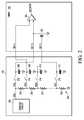
- FIG. 2is a schematic diagram showing further detail of components in the embodiment of the semiconductor device of FIG. 1 .
- FIG. 3is a schematic diagram showing further detail of an embodiment of a comparator that may be used in the timer circuit of FIG. 2 .
- FIG. 4illustrates examples of timing diagrams for various signals used in the semiconductor device of FIG. 1 .
- a timer circuitthat has a near exponential dependence on temperature.
- the timercan be used for a sample and hold system to minimize refresh power at lower temperature since the refresh period is proportional to the leakage on the sample and hold switches.
- the circuitalso runs on very low power, for example, 10 nA of current.
- FIG. 1is a block diagram of an embodiment of a semiconductor device 100 including a exponential to temperature timer 102 , delay module 104 , inverter 105 , AND gate 106 , reference voltage generator 108 , second delay module 110 , and AND gate 112 .
- Exponential to temperature timer 102is coupled to provide a refresh signal to delay module 104 , and to receive an enable refresh signal from an output of AND gate 106 , voltage references (REFA, REFB, REFC) from reference voltage generator 108 , and refresh switch signal from an output of AND gate 112 .
- voltage referencesREFA, REFB, REFC
- the timer 102generates the refresh signal that is used to trigger an edge to turn on band gap circuitry in reference voltage generator 108 and sample all voltages that need to be stored for the semiconductor device 100 , including the three reference voltage signals REFA, REFB, REFC.
- Delay module 104is coupled to receive the refresh signal from exponential to temperature timer 102 , and to provide a first delayed refresh signal as an input to inverter 105 .
- the first delayed refresh signalis inverted by inverter 105 and the inverted first delayed refresh signal is provided as an input to AND gate 106 .
- the refresh signalis provided at another input to AND gate 106 .
- An enable refresh signalis output by AND gate 106 and provided to reference voltage generator 108 .
- Delay module 110receives the refresh signal as an input from exponential to temperature timer 102 and outputs a second delayed reference signal to AND gate 112 .
- Delay module 104 and delay module 110can impose different time delays on the refresh signals. For example, delay module 104 imposes a time delay of 16 microseconds on the refresh signal and delay module 110 imposes a time delay of 4 microseconds on the refresh signal.
- Delay module 110can be used to allow signals in various circuit components, such as a band gap circuit, to settle into steady state values before being used to generate/refresh reference voltages or other signals. Other time delay values can be used for delay modules 104 , 110 .
- AND gate 112receives the second delayed refresh signal at a first input and the refresh signal at a second input, and output a refresh switch signal that is provided as input to reference voltage generator 108 and exponential to temperature timer 102 .
- Reference voltage generator 108can include a band gap circuit, a resistor ladder or resistor divider, multipliers, sample and hold circuits, and other suitable circuits or components. In the embodiment shown, reference voltage generator 108 receives the enable refresh signal from AND gate 106 and the refresh switch signal from AND gate 112 . Reference voltage generator 108 outputs voltage references such as first or “1” through N reference voltage signals (REF 1 , REF 2 , REF 3 . . . REFN) and voltage reference signals (REFA, REFB, REFC) provided to exponential to temperature timer 102 .
- REF 1 , REF 2 , REF 3 . . . REFNvoltage reference signals
- REFA, REFB, REFCvoltage reference signals
- FIG. 2is a schematic diagram showing further detail of some of the components in the embodiment of the semiconductor device 100 of FIG. 1 including a portion of reference voltage generator 108 and a portion of timer 102 .
- band gap circuit 200outputs a band gap voltage signal VBG to resistor divider 202 .
- Resistor divider 202includes resistors 220 , 222 , 224 , 226 coupled in series between the VBG signal and ground.
- ground and “VSS” as used hereinrefer to a voltage level of 0 Volts or a virtual ground signal that is lower than a supply voltage (such as VDD).
- a first voltage supply RDBis tapped to the VBG signal.
- a second voltage supply RDAis tapped between resistors 220 and 222 of resistor ladder 202 .
- a third voltage supply RDNis tapped between resistors 222 and 224 of resistor ladder 202 .
- a fourth voltage supply RDCis tapped between resistors 224 and 226 of resistor ladder 202 .
- the portion of reference voltage generator 108 shownalso includes switches 212 - 218 and capacitors 206 - 211 .
- Switch 212is coupled in series between voltage supply RDB and capacitor 206 .
- One plate of capacitor 206is coupled to the output of switch 212 and a second plate of capacitor 206 is coupled to ground.
- a REFB voltage signalis generated by the operation of refresh switch 212 and capacitor 206 .
- Switch 214is coupled in series between voltage supply RDA and capacitor 208 .
- One plate of second capacitor 208is coupled to the output of switch 214 and a second plate of capacitor 208 is coupled to ground.
- a REFA voltage signalis generated by the operation of refresh switch 214 and capacitor 208 .
- Switch 216is coupled in series between voltage supply RDN and capacitor 210 .
- One plate of a third capacitor 210is coupled to the output of switch 216 and a second plate of capacitor 210 is coupled to ground.
- a REFN voltage signalis generated by the operation of refresh switch 216 and capacitor 210 .
- Switch 218is coupled in series between voltage supply RDC and capacitor 211 .
- One plate of a fourth capacitor 211is coupled to the output of switch 218 and a second plate of capacitor 211 is coupled to ground.
- a REFC voltage signalis generated by the operation of refresh switch 218 and capacitor 211 .
- resistor ladder 202can include any suitable number of resistors to provide the desired number of reference voltages.
- the number and type of reference voltages shown in FIG. 2are only for purpose of example and are not meant to limit the methods and devices disclosed herein.
- the REFA voltage signalis coupled to a positive terminal input of comparator 204 .
- the REFB voltage signalis coupled to a negative terminal input of comparator 204 , and to a drain electrode of N-channel MOS transistor 205 .
- a control gate of transistor 205is coupled to the REFC voltage signal.
- Comparator 204outputs the refresh signal.
- the REFA voltage signalis a stored constant reference to the comparator 204 that is refreshed every timeout of the timer 102 .
- the REFB voltage signalis a pre-charged voltage that will slowly discharge through the transistor 205 until REFB falls below REFA to assert the output of comparator 204 and start a new refresh cycle.
- the REFC voltage signalcan be a trimmed reference voltage from the band gap circuitry and is a constant value that is refreshed periodically.
- the value of the REFC voltage signalis typically below the threshold voltage of transistor 205 .
- REFC voltagemay be approximately 200 mV, whereas threshold voltage to turn on transistor 205 may be around 600 mV or more.
- Semiconductor circuit components including transistor 205typically experience current leakage that varies with temperature. Accordingly, at temperatures where more leakage occurs and higher refresh rates are required to maintain desired levels of reference voltages, transistor 205 can be used to trigger a refresh cycle of reference voltages in reference voltage generator 108 . Since the leakage varies with temperature, the frequency of refresh cycles will vary with temperature, thereby saving power by reducing the number of refresh cycles at lower temperatures where leakage is less pronounced than at higher temperatures.
- transistor 205By keeping the REFC voltage signal below the threshold voltage of transistor 205 , leakage of transistor 205 can still be detected and used to trigger a refresh cycle when the REFB voltage signal reaches a level at or below the level of the REFA voltage signal.
- the sub-threshold characteristics of transistor 205will result in a near exponential response in the rate of change of the REFB voltage.
- FIG. 3is a schematic diagram showing further detail of an embodiment of a comparator 204 that may be used in the timer 108 of FIGS. 1 and 2 including P-channel transistors 302 - 316 , N-channel transistors 318 - 328 and 332 - 336 , OR gate 338 , and inverter 340 .
- Source electrodes of P-channel transistors 302 - 316are coupled to a supply voltage VDD.
- Source electrodes of N-channel transistors 322 , 326 , 328 , 332 , 334 , 336are coupled to ground.
- N-channel transistor 326further has a drain electrode coupled to the REFB voltage signal and a control gate coupled to a comparator output (CMPOUT) signal.
- CMPOUTcomparator output
- P-channel transistor 302further has a drain electrode coupled to a drain electrode of N-channel transistor 328 , and a control gate coupled between the drain electrode of P-channel transistor 304 and the drain electrode of N-channel transistor 318 .
- N-channel transistor 328further has a control gate coupled to control gates of N-channel transistors 332 and 334 .
- the control gate of N-channel transistor 328is also coupled to the drain electrode of N-channel transistor 328 .
- P-channel transistor 304further has a control gate coupled to the control gates of P-channel transistors 306 and 312 and a drain electrode coupled to a drain electrode of N-channel transistor 318 .
- the control gate of P-channel transistor 304is also coupled to the drain electrode of P-channel transistor 304 .
- N-channel transistor 318further has a control gate coupled to the REFB voltage signal and a source electrode coupled to the source electrode of N-channel transistor 320 .
- Tail current source 330is coupled between the source electrodes of N-channel transistors 318 , 320 and ground.
- P-channel transistor 306further has a control gate coupled to the control gate of P-channel transistor 304 and a drain electrode coupled to a drain electrode of N-channel transistor 320 .
- N-channel transistor 320further has a control gate coupled to the REFA voltage signal and a source electrode coupled to the source electrode of N-channel transistor 318 .
- P-channel transistor 308has a gate electrode coupled to the complement of the refresh switch signal, and a drain electrode coupled between the drain electrode of P-channel transistor 306 and the drain electrode of N-channel transistor 320 .
- P-channel transistor 310has a control gate coupled to the drain electrode of P-channel transistor 308 and a drain electrode coupled to the drain electrode of N-channel transistor 332 and the control gate of transistor 322 .
- N-channel transistor 332has a control gate coupled the control gates of N-channel transistors 328 and 334 , and a drain electrode coupled to the drain electrode of P-channel transistor 310 .
- P-channel transistor 312has a control gate coupled the control gates of P-channel transistors 302 , 304 and 306 and a drain electrode coupled to the drain electrode of transistor 322 .
- N-channel transistor 322has a control gate coupled between the drain electrodes of P-channel transistor 310 and N-channel transistor 332 and a drain electrode coupled to the drain of transistor 312 .
- P-channel transistor 314has a control gate coupled to a complement of the refresh switch signal, and a drain electrode coupled between a control gate of transistor 316 and drain electrodes of P-channel transistor 312 and N-channel transistor 322 .
- P-channel transistor 316has a control gate coupled between drain electrodes of P-channel transistors 312 , 314 and N-channel transistor 322 and a drain electrode coupled to the drain electrode of N-channel transistor 334 .
- the comparator output signal CMPOUTis taken as the signal between the drain electrodes of P-channel transistor 316 and N-channel transistor 334 .
- N-channel transistor 336further has a control gate coupled the refresh switch signal, and a drain electrode coupled to the comparator output signal CMPOUT that is coupled to an input of the OR gate 338 .
- a second input to OR gate 338is coupled to the enable refresh signal.
- An input to inverter 340receives the refresh switch signal and the output of inverter 340 is the complement of the refresh switch signal.
- comparator 204will now be described with reference to timing diagrams for various signals shown in FIG. 4 .
- the step segments of the signals at “high” voltage or logic “high” in the timing diagramsare also referred to as “pulses” herein.
- a time history of the relationship of the REFB voltage signal to the REFA voltage signal through a refresh cycleis shown in diagram 402 .
- the REFA voltage signalremains relatively constant at a specified level over time. In the example shown, the REFA voltage signal has a constant value of 0.4 Volts.
- the REFB voltage signaldeclines linearly over time until it reaches a value equal to the value of the REFA voltage signal.
- Transistors 302 , 304 , 306 , 310 , 318 , 320 , 328 and 332 and tail current source 330form a push-pull comparator.
- Transistors 312 , 322form a first inverter and transistors 316 , 334 form a second inverter. The discharging of the REFB voltage signal occurs gradually over time.
- the first and second invertersact as current-starved inverters and are used to prevent slow signals from the push-pull comparator 204 from being input to OR gate 338 until the REFB voltage signal is less than or equal to the REFA voltage signal.
- the value of the comparator output signal CMPOUTgoes high as shown in diagram 404 .
- a high value of the CMPOUT signal at the gate of transistor 326causes transistor 326 to conduct and draw the value the REFB voltage signal to ground, further below the value of the REFA voltage signal.
- OR gate 338With the CMPOUT signal at a high value at an input to OR gate 338 , the OR gate 338 outputs a high value for the refresh signal.
- the refresh signalis coupled to a first input of AND gate 106 , and to delay module 104 .
- Delay module 104outputs a low value until a specified amount of time passes. The low value is inverted to a high value by inverter 105 and provided as a second input to AND gate 106 . With both inputs to AND gate 106 high, the output of AND gate 106 , which in the enable refresh signal shown in diagram 408 is also high. The band gap voltage VBG is refreshed when the enable refresh signal is high, as shown in diagram 410 .
- An additional delaycan be introduced by delay module 110 to provide sufficient time for the value of the band gap voltage signal VBG to settle to a steady state value.
- the refresh signalis provided as input to delay module 110 and AND gate 112 .
- the output of delay module 110will be low for a second specified amount of time, such as 4 microseconds or other suitable value, even though the value of the refresh signal is high.
- the value of the refresh signalwill be passed through to AND gate 112 once the second specified amount of time expires. With both the inputs to the AND gate 112 high, the output of AND gate 112 , which is the refresh switch signal, will be high, as shown in FIG. 412 .
- the refresh switch signalis inverted using inverter 340 and provided to the control gates of transistors 308 and 314 .
- the refresh switch signalis provided to the control gate of transistor 336 .
- transistor 336draws the voltage of the comparator output signal CMPOUT to ground, thereby de-activating the control gate of transistor 326 and allowing the voltage signal REFB to be refreshed by reference voltage generator 108 .
- the delay module 104allows the refresh signal to pass to inverter 105 .
- inverter 105inverts the high refresh signal to a low value, the output of the AND gate 106 will go low, ending the refresh cycle, as shown in diagrams 402 , 408 , 410 , and 412 .
- the voltage signal REFBis then allowed to decay gradually until it reaches the value of the voltage signal REFA, which will initiate the state of another refresh cycle, and so on.
- the time when each refresh cycle beginsdepends on the speed at which the voltage signal REFB discharges until it reaches the value of voltage signal REFA.
- the speed of decayis proportional to the subthreshold leakage of transistor 205 ( FIG. 2 ), which will vary with temperature.
- the variation in the speed of decaymay be exponential or approximately exponential with the rate of leakage increasing as the temperature increases.
- the frequency of the refresh cyclesis proportional to temperature thereby conserving power by refreshing reference voltages only when necessary.
- a circuit with a temperature dependent timercomprising a comparator including a first input, a second input, and an output, the output to provide a timer signal during operation; a transistor including a first current terminal and a control terminal, the first current terminal coupled to the second input of the comparator; a first node coupled to the first input of the comparator; a second node coupled to the second input of the comparator and the first current terminal of the transistor; and a third node coupled to the control terminal of the transistor.
- the third nodeis biased to place the transistor in a subthreshold region of operation to change a voltage of the second node at a rate dependent upon temperature.
- the output of the comparatorchanges state when the voltage of the second node crosses a voltage of the first node.
- the third nodecan be biased to place the transistor in a subthreshold region of operation to change a voltage of the second node at a rate exponentially dependent upon temperature.
- the circuitcan further comprise a band gap generator.
- the change in state of the comparator outputcan be utilized to activate the band gap generator to provide a voltage.
- the output of the comparatorprovides pulses, wherein a frequency of the pulses is dependent on temperature.
- the circuitcan further comprise a first capacitor including a first terminal coupled to the first node; a second capacitor including a first terminal coupled to the second node; a third capacitor including a first terminal coupled to the third node; and a band gap generator.
- the change in state of the output of the comparatorcan be utilized to activate the band gap generator to provide a voltage at a generator output.
- the voltage at the outputcan be used to charge the first capacitor, the second capacitor, and the third capacitor for a period of time.
- the circuitcan further comprise a first switch coupled between the generator output and the first capacitor, a second switch coupled between the generator output and the second capacitor, and a third switch coupled between the generator output and the third capacitor.
- the first switch, the second switch, and the third switchare closed at a time based on the change of state of the output of the comparator to charge the first capacitor, the second capacitor, and the third capacitor respectively, with the voltage provided at the generator output.
- the generator outputcan be coupled to a resistor ladder
- the first switchcan be connected to a first node of the resistor ladder
- the second switchcan be connected to a second node of the resistor ladder
- the third switchcan be connected to a third node of the resistor ladder.
- the circuitcan further comprise a first capacitor including a first terminal coupled to the first node; a second capacitor including a first terminal coupled to the second node; and a third capacitor including a first terminal coupled to the third node.
- the first capacitor, second capacitor, and third capacitorare charged at a frequency that can be dependent upon the rate of discharge of the voltage.
- the circuitcan further comprise a capacitor.
- the second nodecan be coupled to the capacitor.
- the capacitorcan be discharged through the transistor.
- the circuitcan further comprise a capacitor.
- the capacitorcan be recharged at a frequency that is dependent upon the rate of change of the voltage.
- the capacitorcan be charged at time determined by the change of state of the output of the comparator.
- the capacitorcan be charged for a predetermined time after the change in state of the output of the comparator.
- the circuitcan further comprise a reference node to provide a reference voltage.
- the reference nodecan be charged at a time determined by the change of state of the output of the comparator.
- the third nodecan be biased to place the transistor in a subthreshold region of operation to discharge a voltage of the second node at a rate dependent upon temperature.
- the output of the comparatorchanges state when the voltage of the second node discharges below the voltage of the first node.
- a method of operating a timercomprising operating a timer to provide pulses at a comparator output wherein a frequency of the pulses can be dependent on temperature.
- Providing each pulseincludes biasing a first input of the comparator at a voltage; and operating a transistor in a subthreshold region of operation to change the voltage of the first input of a comparator at a rate dependent upon temperature.
- the output of the comparatorchanges state when the voltage of the first input crosses a voltage of a second input of the comparator.
- the operating of a transistor in a subthreshold region of operation to change the voltage of the first input of a comparator at a rate dependent upon temperatureincludes operating the transistor in a subthreshold region of operation to change the voltage of the first input of the comparator at a rate exponentially dependent upon temperature.
- the methodcan further comprise using each pulse to refresh a reference voltage of a reference node.
- each pulse to refresh a reference voltagecan include using each pulse to activate a band gap generator to provide a voltage to refresh the reference voltage.
- the band gap generatorcan be deactivated before being activated by a next successive pulse of the pulses.
- the using of each pulse to refresh a reference voltage of a reference nodecan include charging a capacitor coupled to the reference node to refresh the reference voltage.
- each pulse of the pulsescan be used to bias the first input for producing the next successive pulse.
- the first inputcan be coupled to a capacitor that is charged at times based on the pulses.
- the operating of a transistorcan include operating the transistor in a subthreshold region of operation to discharge the voltage of the first input of the comparator at a rate dependent upon temperature, the output of the comparator changes state when the voltage of the first input discharges below the voltage of the second input of the comparator.
- assertor “set” and “negate” (or “deassert” or “clear”) are used herein when referring to the rendering of a signal, status bit, or similar apparatus into its logically true or logically false state, respectively. If the logically true state is a logic level one, the logically false state is a logic level zero. And if the logically true state is a logic level zero, the logically false state is a logic level one.
- Each signal described hereinmay be designed as positive or negative logic, where negative logic can be indicated by a bar over the signal name or “B” (for “bar”) following the name.
- negative logicthe signal is active low where the logically true state corresponds to a logic level zero.
- positive logicthe signal is active high where the logically true state corresponds to a logic level one.
- any of the signals described hereincan be designed as either negative or positive logic signals. Therefore, in alternate embodiments, those signals described as positive logic signals may be implemented as negative logic signals, and those signals described as negative logic signals may be implemented as positive logic signals.
- N-channel transistor 205can be replaced with a P-channel transistor, and corresponding changes in logic comparator 204 . Accordingly, the specification and figures are to be regarded in an illustrative rather than a restrictive sense, and all such modifications are intended to be included within the scope of the present disclosure. Any benefits, advantages, or solutions to problems that are described herein with regard to specific embodiments are not intended to be construed as a critical, required, or essential feature or element of any or all the claims.
- Coupledis not intended to be limited to a direct coupling or a mechanical coupling.
Landscapes
- Engineering & Computer Science (AREA)
- Theoretical Computer Science (AREA)
- Physics & Mathematics (AREA)
- General Physics & Mathematics (AREA)
- General Engineering & Computer Science (AREA)
- Power Engineering (AREA)
- Computer Hardware Design (AREA)
- Microelectronics & Electronic Packaging (AREA)
- Dram (AREA)
- Electronic Switches (AREA)
- Power Sources (AREA)
- Electromagnetism (AREA)
- Radar, Positioning & Navigation (AREA)
- Automation & Control Theory (AREA)
Abstract
Description
Claims (22)
Priority Applications (4)
| Application Number | Priority Date | Filing Date | Title |
|---|---|---|---|
| US13/678,117US8981857B2 (en) | 2012-11-15 | 2012-11-15 | Temperature dependent timer circuit |
| JP2013236015AJP6327742B2 (en) | 2012-11-15 | 2013-11-14 | Temperature dependent timer circuit |
| CN201310573890.0ACN103823494B (en) | 2012-11-15 | 2013-11-15 | The timer circuit related to temperature |
| KR1020130138899AKR102104681B1 (en) | 2012-11-15 | 2013-11-15 | Temperature dependent timer circuit |
Applications Claiming Priority (1)
| Application Number | Priority Date | Filing Date | Title |
|---|---|---|---|
| US13/678,117US8981857B2 (en) | 2012-11-15 | 2012-11-15 | Temperature dependent timer circuit |
Publications (2)
| Publication Number | Publication Date |
|---|---|
| US20140132240A1 US20140132240A1 (en) | 2014-05-15 |
| US8981857B2true US8981857B2 (en) | 2015-03-17 |
Family
ID=50681085
Family Applications (1)
| Application Number | Title | Priority Date | Filing Date |
|---|---|---|---|
| US13/678,117Active2033-06-15US8981857B2 (en) | 2012-11-15 | 2012-11-15 | Temperature dependent timer circuit |
Country Status (4)
| Country | Link |
|---|---|
| US (1) | US8981857B2 (en) |
| JP (1) | JP6327742B2 (en) |
| KR (1) | KR102104681B1 (en) |
| CN (1) | CN103823494B (en) |
Cited By (1)
| Publication number | Priority date | Publication date | Assignee | Title |
|---|---|---|---|---|
| US20250232826A1 (en)* | 2024-01-12 | 2025-07-17 | Qualcomm Incorporated | Multi-reference-voltage sampled-bandgap system |
Families Citing this family (4)
| Publication number | Priority date | Publication date | Assignee | Title |
|---|---|---|---|---|
| US9244440B2 (en) | 2014-11-19 | 2016-01-26 | Oxana S Pantchenko | Temperature dependent device |
| TWI557529B (en)* | 2016-01-12 | 2016-11-11 | 新唐科技股份有限公司 | Reference voltage circuit |
| GB201622029D0 (en) | 2016-12-22 | 2017-02-08 | Nederlands Inst Voor Ecologie (Nioo-Knaw) See Scientia Terrae Vzw Nordic Semiconductor Asa | Voltage sampling circuits |
| CN107204775B (en)* | 2017-06-02 | 2021-02-02 | 广州视源电子科技股份有限公司 | Sampling method and sampling device for analog signals |
Citations (16)
| Publication number | Priority date | Publication date | Assignee | Title |
|---|---|---|---|---|
| US4906865A (en) | 1988-12-09 | 1990-03-06 | Intel Corporation | Sample and hold circuit for temporal associations in a neural network |
| US5184218A (en) | 1991-07-03 | 1993-02-02 | Wavephore, Inc. | Bandwidth compression and expansion system |
| US5479169A (en) | 1994-06-07 | 1995-12-26 | Louisiana Simchip Technologies, Inc. | Multiple neural network analog to digital converter for simultaneously processing multiple samples |
| US5627970A (en) | 1994-08-08 | 1997-05-06 | Lucent Technologies Inc. | Methods and apparatus for achieving and maintaining optimum transmission rates and preventing data loss in a processing system nework |
| US6163225A (en) | 1999-05-05 | 2000-12-19 | Intel Corporation | Method and apparatus for achieving low standby power using a positive temperature correlated clock frequency |
| US6217213B1 (en)* | 1990-05-15 | 2001-04-17 | Dallas Semiconductor Corporation | Temperature sensing systems and methods |
| US7031273B2 (en) | 2004-04-23 | 2006-04-18 | Motorola, Inc. | Session initiation protocol retransmission method |
| US7236061B2 (en) | 2005-05-03 | 2007-06-26 | Macronix International Co., Ltd. | Temperature compensated refresh clock circuit for memory circuits |
| US7276956B2 (en)* | 2004-06-23 | 2007-10-02 | Nec Electronics Corporation | Integrated circuit apparatus controlling source voltage of MOSFET based on temperature |
| US7391196B2 (en)* | 2005-09-30 | 2008-06-24 | Silicon Laboratories Inc. | In system analysis and compensation for a digital PWM controller |
| US7405963B2 (en)* | 2001-04-05 | 2008-07-29 | T-Ram Semiconductor, Inc. | Dynamic data restore in thyristor-based memory device |
| US7515496B2 (en) | 2004-12-10 | 2009-04-07 | Elpida Memory Inc. | Self-refresh timer circuit and method of adjusting self-refresh timer period |
| US7535309B2 (en)* | 2006-05-09 | 2009-05-19 | Fairchild Semiconductor Corporation | Low power, temperature and frequency, tunable, on-chip clock generator |
| US7557665B2 (en) | 2007-03-13 | 2009-07-07 | Taiwan Semiconductor Manufacturing Company, Ltd. | Temperature tracking oscillator circuit |
| US7583059B2 (en) | 2003-12-18 | 2009-09-01 | Lg Chem, Ltd. | Apparatus and method for estimating state of charge of battery using neural network |
| US7808331B2 (en) | 2005-02-28 | 2010-10-05 | Fujitsu Limited | Current-controlled oscillator |
Family Cites Families (8)
| Publication number | Priority date | Publication date | Assignee | Title |
|---|---|---|---|---|
| JPH0973331A (en)* | 1995-06-30 | 1997-03-18 | Seiko Instr Inc | Semiconductor integrated circuit device |
| US5870345A (en)* | 1997-09-04 | 1999-02-09 | Siemens Aktiengesellschaft | Temperature independent oscillator |
| US6510033B1 (en)* | 2000-06-30 | 2003-01-21 | Intel Corporation | RC-timer circuit to reduce current leakage in future semiconductor processes |
| JP2002261608A (en)* | 2001-03-06 | 2002-09-13 | Ricoh Co Ltd | A / D conversion circuit |
| CN100505718C (en)* | 2004-10-28 | 2009-06-24 | 电子科技大学 | A High Speed Burst Mode Clock Data Recovery Circuit |
| US7342463B2 (en)* | 2005-11-15 | 2008-03-11 | Analog Devices, Inc. | Timer circuits and method |
| JP4899738B2 (en)* | 2006-09-15 | 2012-03-21 | 日本電気株式会社 | Semiconductor integrated circuit device |
| JP4791581B2 (en)* | 2009-08-01 | 2011-10-12 | 株式会社半導体理工学研究センター | Power supply voltage control circuit and control method for subthreshold digital CMOS circuit |
- 2012
- 2012-11-15USUS13/678,117patent/US8981857B2/enactiveActive
- 2013
- 2013-11-14JPJP2013236015Apatent/JP6327742B2/enactiveActive
- 2013-11-15CNCN201310573890.0Apatent/CN103823494B/enactiveActive
- 2013-11-15KRKR1020130138899Apatent/KR102104681B1/enactiveActive
Patent Citations (16)
| Publication number | Priority date | Publication date | Assignee | Title |
|---|---|---|---|---|
| US4906865A (en) | 1988-12-09 | 1990-03-06 | Intel Corporation | Sample and hold circuit for temporal associations in a neural network |
| US6217213B1 (en)* | 1990-05-15 | 2001-04-17 | Dallas Semiconductor Corporation | Temperature sensing systems and methods |
| US5184218A (en) | 1991-07-03 | 1993-02-02 | Wavephore, Inc. | Bandwidth compression and expansion system |
| US5479169A (en) | 1994-06-07 | 1995-12-26 | Louisiana Simchip Technologies, Inc. | Multiple neural network analog to digital converter for simultaneously processing multiple samples |
| US5627970A (en) | 1994-08-08 | 1997-05-06 | Lucent Technologies Inc. | Methods and apparatus for achieving and maintaining optimum transmission rates and preventing data loss in a processing system nework |
| US6163225A (en) | 1999-05-05 | 2000-12-19 | Intel Corporation | Method and apparatus for achieving low standby power using a positive temperature correlated clock frequency |
| US7405963B2 (en)* | 2001-04-05 | 2008-07-29 | T-Ram Semiconductor, Inc. | Dynamic data restore in thyristor-based memory device |
| US7583059B2 (en) | 2003-12-18 | 2009-09-01 | Lg Chem, Ltd. | Apparatus and method for estimating state of charge of battery using neural network |
| US7031273B2 (en) | 2004-04-23 | 2006-04-18 | Motorola, Inc. | Session initiation protocol retransmission method |
| US7276956B2 (en)* | 2004-06-23 | 2007-10-02 | Nec Electronics Corporation | Integrated circuit apparatus controlling source voltage of MOSFET based on temperature |
| US7515496B2 (en) | 2004-12-10 | 2009-04-07 | Elpida Memory Inc. | Self-refresh timer circuit and method of adjusting self-refresh timer period |
| US7808331B2 (en) | 2005-02-28 | 2010-10-05 | Fujitsu Limited | Current-controlled oscillator |
| US7236061B2 (en) | 2005-05-03 | 2007-06-26 | Macronix International Co., Ltd. | Temperature compensated refresh clock circuit for memory circuits |
| US7391196B2 (en)* | 2005-09-30 | 2008-06-24 | Silicon Laboratories Inc. | In system analysis and compensation for a digital PWM controller |
| US7535309B2 (en)* | 2006-05-09 | 2009-05-19 | Fairchild Semiconductor Corporation | Low power, temperature and frequency, tunable, on-chip clock generator |
| US7557665B2 (en) | 2007-03-13 | 2009-07-07 | Taiwan Semiconductor Manufacturing Company, Ltd. | Temperature tracking oscillator circuit |
Cited By (1)
| Publication number | Priority date | Publication date | Assignee | Title |
|---|---|---|---|---|
| US20250232826A1 (en)* | 2024-01-12 | 2025-07-17 | Qualcomm Incorporated | Multi-reference-voltage sampled-bandgap system |
Also Published As
| Publication number | Publication date |
|---|---|
| CN103823494B (en) | 2017-09-29 |
| JP6327742B2 (en) | 2018-05-23 |
| CN103823494A (en) | 2014-05-28 |
| US20140132240A1 (en) | 2014-05-15 |
| KR20140063464A (en) | 2014-05-27 |
| KR102104681B1 (en) | 2020-04-24 |
| JP2014099856A (en) | 2014-05-29 |
Similar Documents
| Publication | Publication Date | Title |
|---|---|---|
| US8981857B2 (en) | Temperature dependent timer circuit | |
| US5903506A (en) | Temperature sensitive oscillator circuit | |
| US9356554B2 (en) | Relaxation oscillator with current and voltage offset cancellation | |
| US4428040A (en) | Low power consumption electronic circuit | |
| US4682306A (en) | Self-refresh control circuit for dynamic semiconductor memory device | |
| US20150317496A1 (en) | Method and apparatus for limiting access to an integrated circuit (ic) | |
| KR100524807B1 (en) | Temperature compensated Self Refresh(TCSR) circuit having a temperature sensor limiter | |
| US9997254B2 (en) | Sample-and-hold circuit | |
| US6304148B1 (en) | Oscillator circuit for a semiconductor memory having a temperature dependent cycle | |
| US7038967B2 (en) | Semiconductor apparatus capable of performing refresh control | |
| KR101069678B1 (en) | Temperature Detection Circuit of a Semiconductor Memory Apparatus | |
| US8995216B2 (en) | Semiconductor device with refresh control circuit | |
| CN105786072B (en) | Low dropout regulator, voltage regulator device and driving method thereof | |
| KR100864038B1 (en) | Semiconductor memory device and method for controlling semiconductor memory device | |
| US9007138B2 (en) | Oscillator with startup circuitry | |
| KR20070111334A (en) | Oscillator Circuit and Semiconductor Memory | |
| CN103580651A (en) | Low-phase jitter oscillator | |
| US7187595B2 (en) | Replenishment for internal voltage | |
| US20050057287A1 (en) | Reset generator circuit for generating a reset signal | |
| KR0149225B1 (en) | Direct voltage generater circuit | |
| US9269409B2 (en) | Bit cell write-assistance | |
| US6865136B2 (en) | Timing circuit and method of changing clock period | |
| US8278977B2 (en) | Refresh operation during low power mode configuration | |
| CN203590154U (en) | Oscillator with low phase jitter | |
| US20180294799A1 (en) | Pulsed latch system with state retention and method of operation |
Legal Events
| Date | Code | Title | Description |
|---|---|---|---|
| AS | Assignment | Owner name:FREESCALE SEMICONDUCTOR, INC., TEXAS Free format text:ASSIGNMENT OF ASSIGNORS INTEREST;ASSIGNORS:MCQUIRK, DALE J.;BERENS, MICHAEL T.;NAGDA, MITEN H.;REEL/FRAME:029306/0056 Effective date:20121114 | |
| AS | Assignment | Owner name:CITIBANK, N.A., AS NOTES COLLATERAL AGENT, NEW YORK Free format text:SUPPLEMENT TO IP SECURITY AGREEMENT;ASSIGNOR:FREESCALE SEMICONDUCTOR, INC.;REEL/FRAME:030258/0558 Effective date:20130214 Owner name:CITIBANK, N.A., AS NOTES COLLATERAL AGENT, NEW YORK Free format text:SUPPLEMENT TO IP SECURITY AGREEMENT;ASSIGNOR:FREESCALE SEMICONDUCTOR, INC.;REEL/FRAME:030258/0523 Effective date:20130214 Owner name:CITIBANK, N.A., AS COLLATERAL AGENT, NEW YORK Free format text:SUPPLEMENT TO IP SECURITY AGREEMENT;ASSIGNOR:FREESCALE SEMICONDUCTOR, INC.;REEL/FRAME:030258/0540 Effective date:20130214 Owner name:CITIBANK, N.A., AS NOTES COLLATERAL AGENT, NEW YOR Free format text:SUPPLEMENT TO IP SECURITY AGREEMENT;ASSIGNOR:FREESCALE SEMICONDUCTOR, INC.;REEL/FRAME:030258/0558 Effective date:20130214 Owner name:CITIBANK, N.A., AS NOTES COLLATERAL AGENT, NEW YOR Free format text:SUPPLEMENT TO IP SECURITY AGREEMENT;ASSIGNOR:FREESCALE SEMICONDUCTOR, INC.;REEL/FRAME:030258/0523 Effective date:20130214 | |
| AS | Assignment | Owner name:CITIBANK, N.A., AS NOTES COLLATERAL AGENT, NEW YORK Free format text:SECURITY AGREEMENT;ASSIGNOR:FREESCALE SEMICONDUCTOR, INC.;REEL/FRAME:030633/0424 Effective date:20130521 Owner name:CITIBANK, N.A., AS NOTES COLLATERAL AGENT, NEW YOR Free format text:SECURITY AGREEMENT;ASSIGNOR:FREESCALE SEMICONDUCTOR, INC.;REEL/FRAME:030633/0424 Effective date:20130521 | |
| AS | Assignment | Owner name:CITIBANK, N.A., AS NOTES COLLATERAL AGENT, NEW YORK Free format text:SECURITY AGREEMENT;ASSIGNOR:FREESCALE SEMICONDUCTOR, INC.;REEL/FRAME:031591/0266 Effective date:20131101 Owner name:CITIBANK, N.A., AS NOTES COLLATERAL AGENT, NEW YOR Free format text:SECURITY AGREEMENT;ASSIGNOR:FREESCALE SEMICONDUCTOR, INC.;REEL/FRAME:031591/0266 Effective date:20131101 | |
| STCF | Information on status: patent grant | Free format text:PATENTED CASE | |
| AS | Assignment | Owner name:FREESCALE SEMICONDUCTOR, INC., TEXAS Free format text:PATENT RELEASE;ASSIGNOR:CITIBANK, N.A., AS COLLATERAL AGENT;REEL/FRAME:037357/0685 Effective date:20151207 Owner name:FREESCALE SEMICONDUCTOR, INC., TEXAS Free format text:PATENT RELEASE;ASSIGNOR:CITIBANK, N.A., AS COLLATERAL AGENT;REEL/FRAME:037357/0671 Effective date:20151207 | |
| AS | Assignment | Owner name:MORGAN STANLEY SENIOR FUNDING, INC., MARYLAND Free format text:ASSIGNMENT AND ASSUMPTION OF SECURITY INTEREST IN PATENTS;ASSIGNOR:CITIBANK, N.A.;REEL/FRAME:037486/0517 Effective date:20151207 | |
| AS | Assignment | Owner name:MORGAN STANLEY SENIOR FUNDING, INC., MARYLAND Free format text:ASSIGNMENT AND ASSUMPTION OF SECURITY INTEREST IN PATENTS;ASSIGNOR:CITIBANK, N.A.;REEL/FRAME:037518/0292 Effective date:20151207 | |
| AS | Assignment | Owner name:FREESCALE SEMICONDUCTOR, INC., TEXAS Free format text:PATENT RELEASE;ASSIGNOR:CITIBANK, N.A., AS COLLATERAL AGENT;REEL/FRAME:037494/0312 Effective date:20151207 | |
| AS | Assignment | Owner name:MORGAN STANLEY SENIOR FUNDING, INC., MARYLAND Free format text:SUPPLEMENT TO THE SECURITY AGREEMENT;ASSIGNOR:FREESCALE SEMICONDUCTOR, INC.;REEL/FRAME:039138/0001 Effective date:20160525 | |
| AS | Assignment | Owner name:NXP, B.V., F/K/A FREESCALE SEMICONDUCTOR, INC., NETHERLANDS Free format text:RELEASE BY SECURED PARTY;ASSIGNOR:MORGAN STANLEY SENIOR FUNDING, INC.;REEL/FRAME:040925/0001 Effective date:20160912 Owner name:NXP, B.V., F/K/A FREESCALE SEMICONDUCTOR, INC., NE Free format text:RELEASE BY SECURED PARTY;ASSIGNOR:MORGAN STANLEY SENIOR FUNDING, INC.;REEL/FRAME:040925/0001 Effective date:20160912 | |
| AS | Assignment | Owner name:NXP B.V., NETHERLANDS Free format text:RELEASE BY SECURED PARTY;ASSIGNOR:MORGAN STANLEY SENIOR FUNDING, INC.;REEL/FRAME:040928/0001 Effective date:20160622 | |
| AS | Assignment | Owner name:NXP USA, INC., TEXAS Free format text:MERGER;ASSIGNOR:FREESCALE SEMICONDUCTOR, INC.;REEL/FRAME:041144/0363 Effective date:20161107 | |
| AS | Assignment | Owner name:MORGAN STANLEY SENIOR FUNDING, INC., MARYLAND Free format text:CORRECTIVE ASSIGNMENT TO CORRECT THE REMOVE PATENTS 8108266 AND 8062324 AND REPLACE THEM WITH 6108266 AND 8060324 PREVIOUSLY RECORDED ON REEL 037518 FRAME 0292. ASSIGNOR(S) HEREBY CONFIRMS THE ASSIGNMENT AND ASSUMPTION OF SECURITY INTEREST IN PATENTS;ASSIGNOR:CITIBANK, N.A.;REEL/FRAME:041703/0536 Effective date:20151207 | |
| MAFP | Maintenance fee payment | Free format text:PAYMENT OF MAINTENANCE FEE, 4TH YEAR, LARGE ENTITY (ORIGINAL EVENT CODE: M1551) Year of fee payment:4 | |
| AS | Assignment | Owner name:SHENZHEN XINGUODU TECHNOLOGY CO., LTD., CHINA Free format text:CORRECTIVE ASSIGNMENT TO CORRECT THE TO CORRECT THE APPLICATION NO. FROM 13,883,290 TO 13,833,290 PREVIOUSLY RECORDED ON REEL 041703 FRAME 0536. ASSIGNOR(S) HEREBY CONFIRMS THE THE ASSIGNMENT AND ASSUMPTION OF SECURITYINTEREST IN PATENTS.;ASSIGNOR:MORGAN STANLEY SENIOR FUNDING, INC.;REEL/FRAME:048734/0001 Effective date:20190217 | |
| AS | Assignment | Owner name:NXP B.V., NETHERLANDS Free format text:RELEASE BY SECURED PARTY;ASSIGNOR:MORGAN STANLEY SENIOR FUNDING, INC.;REEL/FRAME:050744/0097 Effective date:20190903 | |
| AS | Assignment | Owner name:MORGAN STANLEY SENIOR FUNDING, INC., MARYLAND Free format text:CORRECTIVE ASSIGNMENT TO CORRECT THE REMOVE APPLICATION11759915 AND REPLACE IT WITH APPLICATION 11759935 PREVIOUSLY RECORDED ON REEL 037486 FRAME 0517. ASSIGNOR(S) HEREBY CONFIRMS THE ASSIGNMENT AND ASSUMPTION OF SECURITYINTEREST IN PATENTS;ASSIGNOR:CITIBANK, N.A.;REEL/FRAME:053547/0421 Effective date:20151207 | |
| AS | Assignment | Owner name:NXP B.V., NETHERLANDS Free format text:CORRECTIVE ASSIGNMENT TO CORRECT THE REMOVEAPPLICATION 11759915 AND REPLACE IT WITH APPLICATION11759935 PREVIOUSLY RECORDED ON REEL 040928 FRAME 0001. ASSIGNOR(S) HEREBY CONFIRMS THE RELEASE OF SECURITYINTEREST;ASSIGNOR:MORGAN STANLEY SENIOR FUNDING, INC.;REEL/FRAME:052915/0001 Effective date:20160622 | |
| AS | Assignment | Owner name:NXP, B.V. F/K/A FREESCALE SEMICONDUCTOR, INC., NETHERLANDS Free format text:CORRECTIVE ASSIGNMENT TO CORRECT THE REMOVEAPPLICATION 11759915 AND REPLACE IT WITH APPLICATION11759935 PREVIOUSLY RECORDED ON REEL 040925 FRAME 0001. ASSIGNOR(S) HEREBY CONFIRMS THE RELEASE OF SECURITYINTEREST;ASSIGNOR:MORGAN STANLEY SENIOR FUNDING, INC.;REEL/FRAME:052917/0001 Effective date:20160912 | |
| MAFP | Maintenance fee payment | Free format text:PAYMENT OF MAINTENANCE FEE, 8TH YEAR, LARGE ENTITY (ORIGINAL EVENT CODE: M1552); ENTITY STATUS OF PATENT OWNER: LARGE ENTITY Year of fee payment:8 |