US8981579B2 - Impedance controlled packages with metal sheet or 2-layer rdl - Google Patents
Impedance controlled packages with metal sheet or 2-layer rdlDownload PDFInfo
- Publication number
- US8981579B2 US8981579B2US14/306,947US201414306947AUS8981579B2US 8981579 B2US8981579 B2US 8981579B2US 201414306947 AUS201414306947 AUS 201414306947AUS 8981579 B2US8981579 B2US 8981579B2
- Authority
- US
- United States
- Prior art keywords
- microelectronic
- bond
- contacts
- assembly
- trace
- Prior art date
- Legal status (The legal status is an assumption and is not a legal conclusion. Google has not performed a legal analysis and makes no representation as to the accuracy of the status listed.)
- Expired - Fee Related
Links
Images


Classifications
- H—ELECTRICITY
- H01—ELECTRIC ELEMENTS
- H01L—SEMICONDUCTOR DEVICES NOT COVERED BY CLASS H10
- H01L23/00—Details of semiconductor or other solid state devices
- H01L23/58—Structural electrical arrangements for semiconductor devices not otherwise provided for, e.g. in combination with batteries
- H01L23/64—Impedance arrangements
- H—ELECTRICITY
- H01—ELECTRIC ELEMENTS
- H01L—SEMICONDUCTOR DEVICES NOT COVERED BY CLASS H10
- H01L23/00—Details of semiconductor or other solid state devices
- H01L23/28—Encapsulations, e.g. encapsulating layers, coatings, e.g. for protection
- H01L23/31—Encapsulations, e.g. encapsulating layers, coatings, e.g. for protection characterised by the arrangement or shape
- H01L23/3107—Encapsulations, e.g. encapsulating layers, coatings, e.g. for protection characterised by the arrangement or shape the device being completely enclosed
- H01L23/3121—Encapsulations, e.g. encapsulating layers, coatings, e.g. for protection characterised by the arrangement or shape the device being completely enclosed a substrate forming part of the encapsulation
- H01L23/3128—Encapsulations, e.g. encapsulating layers, coatings, e.g. for protection characterised by the arrangement or shape the device being completely enclosed a substrate forming part of the encapsulation the substrate having spherical bumps for external connection
- H—ELECTRICITY
- H01—ELECTRIC ELEMENTS
- H01L—SEMICONDUCTOR DEVICES NOT COVERED BY CLASS H10
- H01L23/00—Details of semiconductor or other solid state devices
- H01L23/552—Protection against radiation, e.g. light or electromagnetic waves
- H—ELECTRICITY
- H01—ELECTRIC ELEMENTS
- H01L—SEMICONDUCTOR DEVICES NOT COVERED BY CLASS H10
- H01L24/00—Arrangements for connecting or disconnecting semiconductor or solid-state bodies; Methods or apparatus related thereto
- H01L24/01—Means for bonding being attached to, or being formed on, the surface to be connected, e.g. chip-to-package, die-attach, "first-level" interconnects; Manufacturing methods related thereto
- H01L24/02—Bonding areas ; Manufacturing methods related thereto
- H01L24/04—Structure, shape, material or disposition of the bonding areas prior to the connecting process
- H01L24/06—Structure, shape, material or disposition of the bonding areas prior to the connecting process of a plurality of bonding areas
- H—ELECTRICITY
- H01—ELECTRIC ELEMENTS
- H01L—SEMICONDUCTOR DEVICES NOT COVERED BY CLASS H10
- H01L24/00—Arrangements for connecting or disconnecting semiconductor or solid-state bodies; Methods or apparatus related thereto
- H01L24/01—Means for bonding being attached to, or being formed on, the surface to be connected, e.g. chip-to-package, die-attach, "first-level" interconnects; Manufacturing methods related thereto
- H01L24/42—Wire connectors; Manufacturing methods related thereto
- H01L24/44—Structure, shape, material or disposition of the wire connectors prior to the connecting process
- H01L24/45—Structure, shape, material or disposition of the wire connectors prior to the connecting process of an individual wire connector
- H—ELECTRICITY
- H01—ELECTRIC ELEMENTS
- H01L—SEMICONDUCTOR DEVICES NOT COVERED BY CLASS H10
- H01L24/00—Arrangements for connecting or disconnecting semiconductor or solid-state bodies; Methods or apparatus related thereto
- H01L24/01—Means for bonding being attached to, or being formed on, the surface to be connected, e.g. chip-to-package, die-attach, "first-level" interconnects; Manufacturing methods related thereto
- H01L24/42—Wire connectors; Manufacturing methods related thereto
- H01L24/47—Structure, shape, material or disposition of the wire connectors after the connecting process
- H01L24/49—Structure, shape, material or disposition of the wire connectors after the connecting process of a plurality of wire connectors
- H—ELECTRICITY
- H01—ELECTRIC ELEMENTS
- H01L—SEMICONDUCTOR DEVICES NOT COVERED BY CLASS H10
- H01L25/00—Assemblies consisting of a plurality of semiconductor or other solid state devices
- H01L25/03—Assemblies consisting of a plurality of semiconductor or other solid state devices all the devices being of a type provided for in a single subclass of subclasses H10B, H10D, H10F, H10H, H10K or H10N, e.g. assemblies of rectifier diodes
- H01L25/04—Assemblies consisting of a plurality of semiconductor or other solid state devices all the devices being of a type provided for in a single subclass of subclasses H10B, H10D, H10F, H10H, H10K or H10N, e.g. assemblies of rectifier diodes the devices not having separate containers
- H01L25/065—Assemblies consisting of a plurality of semiconductor or other solid state devices all the devices being of a type provided for in a single subclass of subclasses H10B, H10D, H10F, H10H, H10K or H10N, e.g. assemblies of rectifier diodes the devices not having separate containers the devices being of a type provided for in group H10D89/00
- H01L25/0657—Stacked arrangements of devices
- H—ELECTRICITY
- H01—ELECTRIC ELEMENTS
- H01L—SEMICONDUCTOR DEVICES NOT COVERED BY CLASS H10
- H01L2224/00—Indexing scheme for arrangements for connecting or disconnecting semiconductor or solid-state bodies and methods related thereto as covered by H01L24/00
- H01L2224/01—Means for bonding being attached to, or being formed on, the surface to be connected, e.g. chip-to-package, die-attach, "first-level" interconnects; Manufacturing methods related thereto
- H01L2224/02—Bonding areas; Manufacturing methods related thereto
- H01L2224/023—Redistribution layers [RDL] for bonding areas
- H01L2224/0231—Manufacturing methods of the redistribution layers
- H01L2224/02311—Additive methods
- H—ELECTRICITY
- H01—ELECTRIC ELEMENTS
- H01L—SEMICONDUCTOR DEVICES NOT COVERED BY CLASS H10
- H01L2224/00—Indexing scheme for arrangements for connecting or disconnecting semiconductor or solid-state bodies and methods related thereto as covered by H01L24/00
- H01L2224/01—Means for bonding being attached to, or being formed on, the surface to be connected, e.g. chip-to-package, die-attach, "first-level" interconnects; Manufacturing methods related thereto
- H01L2224/02—Bonding areas; Manufacturing methods related thereto
- H01L2224/023—Redistribution layers [RDL] for bonding areas
- H01L2224/0231—Manufacturing methods of the redistribution layers
- H01L2224/02313—Subtractive methods
- H—ELECTRICITY
- H01—ELECTRIC ELEMENTS
- H01L—SEMICONDUCTOR DEVICES NOT COVERED BY CLASS H10
- H01L2224/00—Indexing scheme for arrangements for connecting or disconnecting semiconductor or solid-state bodies and methods related thereto as covered by H01L24/00
- H01L2224/01—Means for bonding being attached to, or being formed on, the surface to be connected, e.g. chip-to-package, die-attach, "first-level" interconnects; Manufacturing methods related thereto
- H01L2224/02—Bonding areas; Manufacturing methods related thereto
- H01L2224/023—Redistribution layers [RDL] for bonding areas
- H01L2224/0237—Disposition of the redistribution layers
- H01L2224/02375—Top view
- H—ELECTRICITY
- H01—ELECTRIC ELEMENTS
- H01L—SEMICONDUCTOR DEVICES NOT COVERED BY CLASS H10
- H01L2224/00—Indexing scheme for arrangements for connecting or disconnecting semiconductor or solid-state bodies and methods related thereto as covered by H01L24/00
- H01L2224/01—Means for bonding being attached to, or being formed on, the surface to be connected, e.g. chip-to-package, die-attach, "first-level" interconnects; Manufacturing methods related thereto
- H01L2224/02—Bonding areas; Manufacturing methods related thereto
- H01L2224/023—Redistribution layers [RDL] for bonding areas
- H01L2224/0237—Disposition of the redistribution layers
- H01L2224/02379—Fan-out arrangement
- H—ELECTRICITY
- H01—ELECTRIC ELEMENTS
- H01L—SEMICONDUCTOR DEVICES NOT COVERED BY CLASS H10
- H01L2224/00—Indexing scheme for arrangements for connecting or disconnecting semiconductor or solid-state bodies and methods related thereto as covered by H01L24/00
- H01L2224/01—Means for bonding being attached to, or being formed on, the surface to be connected, e.g. chip-to-package, die-attach, "first-level" interconnects; Manufacturing methods related thereto
- H01L2224/02—Bonding areas; Manufacturing methods related thereto
- H01L2224/04—Structure, shape, material or disposition of the bonding areas prior to the connecting process
- H01L2224/04042—Bonding areas specifically adapted for wire connectors, e.g. wirebond pads
- H—ELECTRICITY
- H01—ELECTRIC ELEMENTS
- H01L—SEMICONDUCTOR DEVICES NOT COVERED BY CLASS H10
- H01L2224/00—Indexing scheme for arrangements for connecting or disconnecting semiconductor or solid-state bodies and methods related thereto as covered by H01L24/00
- H01L2224/01—Means for bonding being attached to, or being formed on, the surface to be connected, e.g. chip-to-package, die-attach, "first-level" interconnects; Manufacturing methods related thereto
- H01L2224/02—Bonding areas; Manufacturing methods related thereto
- H01L2224/04—Structure, shape, material or disposition of the bonding areas prior to the connecting process
- H01L2224/05—Structure, shape, material or disposition of the bonding areas prior to the connecting process of an individual bonding area
- H01L2224/0554—External layer
- H01L2224/0555—Shape
- H01L2224/05552—Shape in top view
- H01L2224/05554—Shape in top view being square
- H—ELECTRICITY
- H01—ELECTRIC ELEMENTS
- H01L—SEMICONDUCTOR DEVICES NOT COVERED BY CLASS H10
- H01L2224/00—Indexing scheme for arrangements for connecting or disconnecting semiconductor or solid-state bodies and methods related thereto as covered by H01L24/00
- H01L2224/01—Means for bonding being attached to, or being formed on, the surface to be connected, e.g. chip-to-package, die-attach, "first-level" interconnects; Manufacturing methods related thereto
- H01L2224/26—Layer connectors, e.g. plate connectors, solder or adhesive layers; Manufacturing methods related thereto
- H01L2224/31—Structure, shape, material or disposition of the layer connectors after the connecting process
- H01L2224/32—Structure, shape, material or disposition of the layer connectors after the connecting process of an individual layer connector
- H01L2224/321—Disposition
- H01L2224/32151—Disposition the layer connector connecting between a semiconductor or solid-state body and an item not being a semiconductor or solid-state body, e.g. chip-to-substrate, chip-to-passive
- H01L2224/32221—Disposition the layer connector connecting between a semiconductor or solid-state body and an item not being a semiconductor or solid-state body, e.g. chip-to-substrate, chip-to-passive the body and the item being stacked
- H01L2224/32225—Disposition the layer connector connecting between a semiconductor or solid-state body and an item not being a semiconductor or solid-state body, e.g. chip-to-substrate, chip-to-passive the body and the item being stacked the item being non-metallic, e.g. insulating substrate with or without metallisation
- H—ELECTRICITY
- H01—ELECTRIC ELEMENTS
- H01L—SEMICONDUCTOR DEVICES NOT COVERED BY CLASS H10
- H01L2224/00—Indexing scheme for arrangements for connecting or disconnecting semiconductor or solid-state bodies and methods related thereto as covered by H01L24/00
- H01L2224/01—Means for bonding being attached to, or being formed on, the surface to be connected, e.g. chip-to-package, die-attach, "first-level" interconnects; Manufacturing methods related thereto
- H01L2224/42—Wire connectors; Manufacturing methods related thereto
- H01L2224/44—Structure, shape, material or disposition of the wire connectors prior to the connecting process
- H01L2224/45—Structure, shape, material or disposition of the wire connectors prior to the connecting process of an individual wire connector
- H01L2224/45001—Core members of the connector
- H01L2224/4501—Shape
- H01L2224/45012—Cross-sectional shape
- H01L2224/45015—Cross-sectional shape being circular
- H—ELECTRICITY
- H01—ELECTRIC ELEMENTS
- H01L—SEMICONDUCTOR DEVICES NOT COVERED BY CLASS H10
- H01L2224/00—Indexing scheme for arrangements for connecting or disconnecting semiconductor or solid-state bodies and methods related thereto as covered by H01L24/00
- H01L2224/01—Means for bonding being attached to, or being formed on, the surface to be connected, e.g. chip-to-package, die-attach, "first-level" interconnects; Manufacturing methods related thereto
- H01L2224/42—Wire connectors; Manufacturing methods related thereto
- H01L2224/44—Structure, shape, material or disposition of the wire connectors prior to the connecting process
- H01L2224/45—Structure, shape, material or disposition of the wire connectors prior to the connecting process of an individual wire connector
- H01L2224/45001—Core members of the connector
- H01L2224/45099—Material
- H01L2224/451—Material with a principal constituent of the material being a metal or a metalloid, e.g. boron (B), silicon (Si), germanium (Ge), arsenic (As), antimony (Sb), tellurium (Te) and polonium (Po), and alloys thereof
- H01L2224/45138—Material with a principal constituent of the material being a metal or a metalloid, e.g. boron (B), silicon (Si), germanium (Ge), arsenic (As), antimony (Sb), tellurium (Te) and polonium (Po), and alloys thereof the principal constituent melting at a temperature of greater than or equal to 950°C and less than 1550°C
- H01L2224/45144—Gold (Au) as principal constituent
- H—ELECTRICITY
- H01—ELECTRIC ELEMENTS
- H01L—SEMICONDUCTOR DEVICES NOT COVERED BY CLASS H10
- H01L2224/00—Indexing scheme for arrangements for connecting or disconnecting semiconductor or solid-state bodies and methods related thereto as covered by H01L24/00
- H01L2224/01—Means for bonding being attached to, or being formed on, the surface to be connected, e.g. chip-to-package, die-attach, "first-level" interconnects; Manufacturing methods related thereto
- H01L2224/42—Wire connectors; Manufacturing methods related thereto
- H01L2224/44—Structure, shape, material or disposition of the wire connectors prior to the connecting process
- H01L2224/45—Structure, shape, material or disposition of the wire connectors prior to the connecting process of an individual wire connector
- H01L2224/45001—Core members of the connector
- H01L2224/45099—Material
- H01L2224/451—Material with a principal constituent of the material being a metal or a metalloid, e.g. boron (B), silicon (Si), germanium (Ge), arsenic (As), antimony (Sb), tellurium (Te) and polonium (Po), and alloys thereof
- H01L2224/45138—Material with a principal constituent of the material being a metal or a metalloid, e.g. boron (B), silicon (Si), germanium (Ge), arsenic (As), antimony (Sb), tellurium (Te) and polonium (Po), and alloys thereof the principal constituent melting at a temperature of greater than or equal to 950°C and less than 1550°C
- H01L2224/45147—Copper (Cu) as principal constituent
- H—ELECTRICITY
- H01—ELECTRIC ELEMENTS
- H01L—SEMICONDUCTOR DEVICES NOT COVERED BY CLASS H10
- H01L2224/00—Indexing scheme for arrangements for connecting or disconnecting semiconductor or solid-state bodies and methods related thereto as covered by H01L24/00
- H01L2224/01—Means for bonding being attached to, or being formed on, the surface to be connected, e.g. chip-to-package, die-attach, "first-level" interconnects; Manufacturing methods related thereto
- H01L2224/42—Wire connectors; Manufacturing methods related thereto
- H01L2224/47—Structure, shape, material or disposition of the wire connectors after the connecting process
- H01L2224/48—Structure, shape, material or disposition of the wire connectors after the connecting process of an individual wire connector
- H01L2224/4805—Shape
- H01L2224/4809—Loop shape
- H01L2224/48091—Arched
- H—ELECTRICITY
- H01—ELECTRIC ELEMENTS
- H01L—SEMICONDUCTOR DEVICES NOT COVERED BY CLASS H10
- H01L2224/00—Indexing scheme for arrangements for connecting or disconnecting semiconductor or solid-state bodies and methods related thereto as covered by H01L24/00
- H01L2224/01—Means for bonding being attached to, or being formed on, the surface to be connected, e.g. chip-to-package, die-attach, "first-level" interconnects; Manufacturing methods related thereto
- H01L2224/42—Wire connectors; Manufacturing methods related thereto
- H01L2224/47—Structure, shape, material or disposition of the wire connectors after the connecting process
- H01L2224/48—Structure, shape, material or disposition of the wire connectors after the connecting process of an individual wire connector
- H01L2224/4805—Shape
- H01L2224/4809—Loop shape
- H01L2224/48095—Kinked
- H—ELECTRICITY
- H01—ELECTRIC ELEMENTS
- H01L—SEMICONDUCTOR DEVICES NOT COVERED BY CLASS H10
- H01L2224/00—Indexing scheme for arrangements for connecting or disconnecting semiconductor or solid-state bodies and methods related thereto as covered by H01L24/00
- H01L2224/01—Means for bonding being attached to, or being formed on, the surface to be connected, e.g. chip-to-package, die-attach, "first-level" interconnects; Manufacturing methods related thereto
- H01L2224/42—Wire connectors; Manufacturing methods related thereto
- H01L2224/47—Structure, shape, material or disposition of the wire connectors after the connecting process
- H01L2224/48—Structure, shape, material or disposition of the wire connectors after the connecting process of an individual wire connector
- H01L2224/481—Disposition
- H01L2224/48151—Connecting between a semiconductor or solid-state body and an item not being a semiconductor or solid-state body, e.g. chip-to-substrate, chip-to-passive
- H01L2224/48221—Connecting between a semiconductor or solid-state body and an item not being a semiconductor or solid-state body, e.g. chip-to-substrate, chip-to-passive the body and the item being stacked
- H01L2224/48225—Connecting between a semiconductor or solid-state body and an item not being a semiconductor or solid-state body, e.g. chip-to-substrate, chip-to-passive the body and the item being stacked the item being non-metallic, e.g. insulating substrate with or without metallisation
- H01L2224/48227—Connecting between a semiconductor or solid-state body and an item not being a semiconductor or solid-state body, e.g. chip-to-substrate, chip-to-passive the body and the item being stacked the item being non-metallic, e.g. insulating substrate with or without metallisation connecting the wire to a bond pad of the item
- H—ELECTRICITY
- H01—ELECTRIC ELEMENTS
- H01L—SEMICONDUCTOR DEVICES NOT COVERED BY CLASS H10
- H01L2224/00—Indexing scheme for arrangements for connecting or disconnecting semiconductor or solid-state bodies and methods related thereto as covered by H01L24/00
- H01L2224/01—Means for bonding being attached to, or being formed on, the surface to be connected, e.g. chip-to-package, die-attach, "first-level" interconnects; Manufacturing methods related thereto
- H01L2224/42—Wire connectors; Manufacturing methods related thereto
- H01L2224/47—Structure, shape, material or disposition of the wire connectors after the connecting process
- H01L2224/49—Structure, shape, material or disposition of the wire connectors after the connecting process of a plurality of wire connectors
- H01L2224/491—Disposition
- H01L2224/4912—Layout
- H01L2224/49175—Parallel arrangements
- H—ELECTRICITY
- H01—ELECTRIC ELEMENTS
- H01L—SEMICONDUCTOR DEVICES NOT COVERED BY CLASS H10
- H01L2224/00—Indexing scheme for arrangements for connecting or disconnecting semiconductor or solid-state bodies and methods related thereto as covered by H01L24/00
- H01L2224/73—Means for bonding being of different types provided for in two or more of groups H01L2224/10, H01L2224/18, H01L2224/26, H01L2224/34, H01L2224/42, H01L2224/50, H01L2224/63, H01L2224/71
- H01L2224/732—Location after the connecting process
- H01L2224/73251—Location after the connecting process on different surfaces
- H01L2224/73265—Layer and wire connectors
- H—ELECTRICITY
- H01—ELECTRIC ELEMENTS
- H01L—SEMICONDUCTOR DEVICES NOT COVERED BY CLASS H10
- H01L2225/00—Details relating to assemblies covered by the group H01L25/00 but not provided for in its subgroups
- H01L2225/03—All the devices being of a type provided for in the same main group of the same subclass of class H10, e.g. assemblies of rectifier diodes
- H01L2225/04—All the devices being of a type provided for in the same main group of the same subclass of class H10, e.g. assemblies of rectifier diodes the devices not having separate containers
- H01L2225/065—All the devices being of a type provided for in the same main group of the same subclass of class H10
- H01L2225/06503—Stacked arrangements of devices
- H01L2225/0651—Wire or wire-like electrical connections from device to substrate
- H—ELECTRICITY
- H01—ELECTRIC ELEMENTS
- H01L—SEMICONDUCTOR DEVICES NOT COVERED BY CLASS H10
- H01L2225/00—Details relating to assemblies covered by the group H01L25/00 but not provided for in its subgroups
- H01L2225/03—All the devices being of a type provided for in the same main group of the same subclass of class H10, e.g. assemblies of rectifier diodes
- H01L2225/04—All the devices being of a type provided for in the same main group of the same subclass of class H10, e.g. assemblies of rectifier diodes the devices not having separate containers
- H01L2225/065—All the devices being of a type provided for in the same main group of the same subclass of class H10
- H01L2225/06503—Stacked arrangements of devices
- H01L2225/06527—Special adaptation of electrical connections, e.g. rewiring, engineering changes, pressure contacts, layout
- H01L2225/06537—Electromagnetic shielding
- H—ELECTRICITY
- H01—ELECTRIC ELEMENTS
- H01L—SEMICONDUCTOR DEVICES NOT COVERED BY CLASS H10
- H01L2225/00—Details relating to assemblies covered by the group H01L25/00 but not provided for in its subgroups
- H01L2225/03—All the devices being of a type provided for in the same main group of the same subclass of class H10, e.g. assemblies of rectifier diodes
- H01L2225/04—All the devices being of a type provided for in the same main group of the same subclass of class H10, e.g. assemblies of rectifier diodes the devices not having separate containers
- H01L2225/065—All the devices being of a type provided for in the same main group of the same subclass of class H10
- H01L2225/06503—Stacked arrangements of devices
- H01L2225/06575—Auxiliary carrier between devices, the carrier having no electrical connection structure
- H—ELECTRICITY
- H01—ELECTRIC ELEMENTS
- H01L—SEMICONDUCTOR DEVICES NOT COVERED BY CLASS H10
- H01L23/00—Details of semiconductor or other solid state devices
- H01L23/48—Arrangements for conducting electric current to or from the solid state body in operation, e.g. leads, terminal arrangements ; Selection of materials therefor
- H01L23/488—Arrangements for conducting electric current to or from the solid state body in operation, e.g. leads, terminal arrangements ; Selection of materials therefor consisting of soldered or bonded constructions
- H01L23/498—Leads, i.e. metallisations or lead-frames on insulating substrates, e.g. chip carriers
- H01L23/49811—Additional leads joined to the metallisation on the insulating substrate, e.g. pins, bumps, wires, flat leads
- H01L23/49816—Spherical bumps on the substrate for external connection, e.g. ball grid arrays [BGA]
- H—ELECTRICITY
- H01—ELECTRIC ELEMENTS
- H01L—SEMICONDUCTOR DEVICES NOT COVERED BY CLASS H10
- H01L24/00—Arrangements for connecting or disconnecting semiconductor or solid-state bodies; Methods or apparatus related thereto
- H01L24/01—Means for bonding being attached to, or being formed on, the surface to be connected, e.g. chip-to-package, die-attach, "first-level" interconnects; Manufacturing methods related thereto
- H01L24/26—Layer connectors, e.g. plate connectors, solder or adhesive layers; Manufacturing methods related thereto
- H01L24/28—Structure, shape, material or disposition of the layer connectors prior to the connecting process
- H01L24/29—Structure, shape, material or disposition of the layer connectors prior to the connecting process of an individual layer connector
- H—ELECTRICITY
- H01—ELECTRIC ELEMENTS
- H01L—SEMICONDUCTOR DEVICES NOT COVERED BY CLASS H10
- H01L24/00—Arrangements for connecting or disconnecting semiconductor or solid-state bodies; Methods or apparatus related thereto
- H01L24/01—Means for bonding being attached to, or being formed on, the surface to be connected, e.g. chip-to-package, die-attach, "first-level" interconnects; Manufacturing methods related thereto
- H01L24/42—Wire connectors; Manufacturing methods related thereto
- H01L24/47—Structure, shape, material or disposition of the wire connectors after the connecting process
- H01L24/48—Structure, shape, material or disposition of the wire connectors after the connecting process of an individual wire connector
- H—ELECTRICITY
- H01—ELECTRIC ELEMENTS
- H01L—SEMICONDUCTOR DEVICES NOT COVERED BY CLASS H10
- H01L24/00—Arrangements for connecting or disconnecting semiconductor or solid-state bodies; Methods or apparatus related thereto
- H01L24/73—Means for bonding being of different types provided for in two or more of groups H01L24/10, H01L24/18, H01L24/26, H01L24/34, H01L24/42, H01L24/50, H01L24/63, H01L24/71
- H—ELECTRICITY
- H01—ELECTRIC ELEMENTS
- H01L—SEMICONDUCTOR DEVICES NOT COVERED BY CLASS H10
- H01L2924/00—Indexing scheme for arrangements or methods for connecting or disconnecting semiconductor or solid-state bodies as covered by H01L24/00
- H—ELECTRICITY
- H01—ELECTRIC ELEMENTS
- H01L—SEMICONDUCTOR DEVICES NOT COVERED BY CLASS H10
- H01L2924/00—Indexing scheme for arrangements or methods for connecting or disconnecting semiconductor or solid-state bodies as covered by H01L24/00
- H01L2924/0001—Technical content checked by a classifier
- H01L2924/00012—Relevant to the scope of the group, the symbol of which is combined with the symbol of this group
- H—ELECTRICITY
- H01—ELECTRIC ELEMENTS
- H01L—SEMICONDUCTOR DEVICES NOT COVERED BY CLASS H10
- H01L2924/00—Indexing scheme for arrangements or methods for connecting or disconnecting semiconductor or solid-state bodies as covered by H01L24/00
- H01L2924/0001—Technical content checked by a classifier
- H01L2924/00014—Technical content checked by a classifier the subject-matter covered by the group, the symbol of which is combined with the symbol of this group, being disclosed without further technical details
- H—ELECTRICITY
- H01—ELECTRIC ELEMENTS
- H01L—SEMICONDUCTOR DEVICES NOT COVERED BY CLASS H10
- H01L2924/00—Indexing scheme for arrangements or methods for connecting or disconnecting semiconductor or solid-state bodies as covered by H01L24/00
- H01L2924/01—Chemical elements
- H01L2924/01005—Boron [B]
- H—ELECTRICITY
- H01—ELECTRIC ELEMENTS
- H01L—SEMICONDUCTOR DEVICES NOT COVERED BY CLASS H10
- H01L2924/00—Indexing scheme for arrangements or methods for connecting or disconnecting semiconductor or solid-state bodies as covered by H01L24/00
- H01L2924/01—Chemical elements
- H01L2924/01019—Potassium [K]
- H—ELECTRICITY
- H01—ELECTRIC ELEMENTS
- H01L—SEMICONDUCTOR DEVICES NOT COVERED BY CLASS H10
- H01L2924/00—Indexing scheme for arrangements or methods for connecting or disconnecting semiconductor or solid-state bodies as covered by H01L24/00
- H01L2924/01—Chemical elements
- H01L2924/01029—Copper [Cu]
- H—ELECTRICITY
- H01—ELECTRIC ELEMENTS
- H01L—SEMICONDUCTOR DEVICES NOT COVERED BY CLASS H10
- H01L2924/00—Indexing scheme for arrangements or methods for connecting or disconnecting semiconductor or solid-state bodies as covered by H01L24/00
- H01L2924/01—Chemical elements
- H01L2924/01033—Arsenic [As]
- H—ELECTRICITY
- H01—ELECTRIC ELEMENTS
- H01L—SEMICONDUCTOR DEVICES NOT COVERED BY CLASS H10
- H01L2924/00—Indexing scheme for arrangements or methods for connecting or disconnecting semiconductor or solid-state bodies as covered by H01L24/00
- H01L2924/01—Chemical elements
- H01L2924/01047—Silver [Ag]
- H—ELECTRICITY
- H01—ELECTRIC ELEMENTS
- H01L—SEMICONDUCTOR DEVICES NOT COVERED BY CLASS H10
- H01L2924/00—Indexing scheme for arrangements or methods for connecting or disconnecting semiconductor or solid-state bodies as covered by H01L24/00
- H01L2924/01—Chemical elements
- H01L2924/01079—Gold [Au]
- H—ELECTRICITY
- H01—ELECTRIC ELEMENTS
- H01L—SEMICONDUCTOR DEVICES NOT COVERED BY CLASS H10
- H01L2924/00—Indexing scheme for arrangements or methods for connecting or disconnecting semiconductor or solid-state bodies as covered by H01L24/00
- H01L2924/013—Alloys
- H01L2924/014—Solder alloys
- H—ELECTRICITY
- H01—ELECTRIC ELEMENTS
- H01L—SEMICONDUCTOR DEVICES NOT COVERED BY CLASS H10
- H01L2924/00—Indexing scheme for arrangements or methods for connecting or disconnecting semiconductor or solid-state bodies as covered by H01L24/00
- H01L2924/06—Polymers
- H01L2924/078—Adhesive characteristics other than chemical
- H01L2924/07802—Adhesive characteristics other than chemical not being an ohmic electrical conductor
- H—ELECTRICITY
- H01—ELECTRIC ELEMENTS
- H01L—SEMICONDUCTOR DEVICES NOT COVERED BY CLASS H10
- H01L2924/00—Indexing scheme for arrangements or methods for connecting or disconnecting semiconductor or solid-state bodies as covered by H01L24/00
- H01L2924/10—Details of semiconductor or other solid state devices to be connected
- H01L2924/1015—Shape
- H01L2924/1016—Shape being a cuboid
- H01L2924/10161—Shape being a cuboid with a rectangular active surface
- H—ELECTRICITY
- H01—ELECTRIC ELEMENTS
- H01L—SEMICONDUCTOR DEVICES NOT COVERED BY CLASS H10
- H01L2924/00—Indexing scheme for arrangements or methods for connecting or disconnecting semiconductor or solid-state bodies as covered by H01L24/00
- H01L2924/15—Details of package parts other than the semiconductor or other solid state devices to be connected
- H01L2924/151—Die mounting substrate
- H01L2924/153—Connection portion
- H01L2924/1531—Connection portion the connection portion being formed only on the surface of the substrate opposite to the die mounting surface
- H01L2924/15311—Connection portion the connection portion being formed only on the surface of the substrate opposite to the die mounting surface being a ball array, e.g. BGA
- H—ELECTRICITY
- H01—ELECTRIC ELEMENTS
- H01L—SEMICONDUCTOR DEVICES NOT COVERED BY CLASS H10
- H01L2924/00—Indexing scheme for arrangements or methods for connecting or disconnecting semiconductor or solid-state bodies as covered by H01L24/00
- H01L2924/15—Details of package parts other than the semiconductor or other solid state devices to be connected
- H01L2924/181—Encapsulation
- H—ELECTRICITY
- H01—ELECTRIC ELEMENTS
- H01L—SEMICONDUCTOR DEVICES NOT COVERED BY CLASS H10
- H01L2924/00—Indexing scheme for arrangements or methods for connecting or disconnecting semiconductor or solid-state bodies as covered by H01L24/00
- H01L2924/19—Details of hybrid assemblies other than the semiconductor or other solid state devices to be connected
- H01L2924/191—Disposition
- H01L2924/19101—Disposition of discrete passive components
- H01L2924/19107—Disposition of discrete passive components off-chip wires
- H—ELECTRICITY
- H01—ELECTRIC ELEMENTS
- H01L—SEMICONDUCTOR DEVICES NOT COVERED BY CLASS H10
- H01L2924/00—Indexing scheme for arrangements or methods for connecting or disconnecting semiconductor or solid-state bodies as covered by H01L24/00
- H01L2924/30—Technical effects
- H01L2924/301—Electrical effects
- H01L2924/30107—Inductance
- H—ELECTRICITY
- H01—ELECTRIC ELEMENTS
- H01L—SEMICONDUCTOR DEVICES NOT COVERED BY CLASS H10
- H01L2924/00—Indexing scheme for arrangements or methods for connecting or disconnecting semiconductor or solid-state bodies as covered by H01L24/00
- H01L2924/30—Technical effects
- H01L2924/301—Electrical effects
- H01L2924/3011—Impedance
Definitions
- Microelectronic chipsare typically flat bodies with oppositely facing, generally planar front and rear surfaces with edges extending between these surfaces. Chips generally have contacts, sometimes also referred to as pads or bond pads, on the front surface which are electrically connected to the circuits within the chip. Chips are typically packaged by enclosing them with a suitable material to form microelectronic packages having terminals that are electrically connected to the chip contacts. The package may then be connected to test equipment to determine whether the packaged device conforms to a desired performance standard.
- the packagemay be connected to a larger circuit (e.g., a circuit in an electronic product such as a computer or a cell phone) by connecting the package terminals to matching lands on a printed circuit board (PCB) by a suitable connection method such as soldering.
- a larger circuite.g., a circuit in an electronic product such as a computer or a cell phone
- PCBprinted circuit board
- Microelectronic packagesmay be fabricated at the wafer level; that is, the enclosure, terminations and other features that constitute the package, are fabricated while the chips, or die, are still in a wafer form. After the die have been formed, the wafer is subject to a number of additional process steps to form the package structure on the wafer, and the wafer is then diced to free the individually packaged die. Wafer level processing can be an efficient fabrication method because the footprint of each die package may be made identical, or nearly identical, to the size of the die itself, resulting in very efficient utilization of area on the printed circuit board to which the packaged die is attached.
- a common technique for forming electrically conductive connections between a microelectronic chip and one or more other electronic componentsis through wirebonding.
- a wirebonding toolattaches the end of a wire to a pad on a microelectronic chip using thermal and/or ultrasonic energy and then loops the wire to a contact on the other electronic component and forms a second bond thereto using thermal and/or ultrasonic forces.
- a microelectronic assemblyincludes an interconnection element, a microelectronic device, a plurality of raised conductive elements, a surface conductive element, and a bond element.
- the interconnection elementmay be a dielectric element that has a plurality of element contacts and at least one reference contact on the surface of the interconnection element.
- the microelectronic deviceoverlies the dielectric element and has a rear surface overlying the dielectric element, an opposed front surface with device contacts exposed thereat, and at least one surface conductive element attached to the front surface.
- a plurality of raised conductive elementsmay connect the device contacts with the element contacts.
- the raised conductive elementsmay have substantial portions spaced a first height above and extending at least generally parallel to at least one surface conductive element, such that a desired impedance may be achieved for the raised conductive elements.
- a bond elementmay electrically connect at least one surface conductive element with at least one reference contact that may be connectable to a source of reference potential.
- substantial portions of each of the conductive elementsmay be a length that is at least 25% of the total length of each conductive element.
- the substantial portion of each conductive elementmay be at least 1 millimeter.
- the first and second edgesmay meet at a corner of the microelectronic device.
- the bond elementmay be a first bond element extending beyond a first edge of the microelectronic device. There may also be a second bond element extending beyond a second edge of the microelectronic device and connecting the at least one surface conductive element to a second reference contact of the interconnection element.
- the bond elementmay be positioned between at least two of the plurality of raised conductive elements.
- the bond elementmay extend in a direction transverse to the direction in which at least some of the plurality of raised conductive elements extend.
- At least one of the plurality of raised conductive elementsextends beyond a first edge of the microelectronic device and the bond element extends beyond the first edge.
- the raised conductive elementsmay include bond wires.
- all of the conductive elementsare bond wires.
- the surface conductive elementmay be a power plane, a ground plane, or a combination of a power and ground plane.
- the surface conductive elementmay also be connectable to a fixed voltage source.
- the surface conductive elementmay further reduce an inductance in the electrical connection between the device contact and a source of fixed voltage.
- the surface conductive elementmay be comprised of multiple sections, wherein at least a first section may be a power plane and a second section may be a ground plane.
- the first sectionmay be adjacent one edge of the device contacts and the second section may be adjacent the opposed edge of the device contacts.
- the first and second sectionsmay be adjacent the same edge of the device contacts.
- the first sectionmay be further comprised of a first portion and a second portion, wherein device contacts extend therebetween.
- theremay be another bond element that electrically connects the first and second portions of the first section.
- the second sectionmay also be further comprised of a first portion and a second portion, and the device contacts may also further extend therebetween.
- Another bond elementmay be used to electrically connect the first and second portions of the second section.
- another bond elementmay be used to electrically connect device contacts with the first portion or second portion of at least one of the first section and second sections.
- another bond elementmay connect at least one device contact with at least one surface conductive element.
- a microelectronic assemblyincludes an interconnection element having a face, a microelectronic device, a metal plane, and first and second bond elements.
- the microelectronic devicemay overly the face of the interconnection element and may have a plurality of first device contacts disposed the surface of the microelectronic device.
- An at least one second device contactmay also be disposed at the surface and at least one trace may be deposited on the surface and electrically connected to the interconnection element.
- the at least one tracemay electrically connect at least one of the first device contacts with the at least one second device contact.
- At least one first bond elementelectrically connects the at least one second device contact with at least one of the element contacts.
- At least one metal planemay be electrically connected to the interconnection element and attached to the microelectronic device at a height from the surface greater than a height of the at least one trace from the surface.
- the at least one metal planemay be connectable to a source of reference potential, such that a desired impedance may be achieved for the at least one trace.
- the at least one tracemay have at least a substantial portion extending in a direction substantially parallel to a direction in which the metal plane extends.
- At least one bond elementelectrically connects the metal plane with a reference element of the interconnection element, which may be electrically connectable with a source of reference potential.
- the substantial portion of the at least one tracemay be a length that is at least 25% of the total length of the at least one trace or have a length of at least 1 millimeter.
- the second bond elementextends beyond a first edge of the microelectronic device, and the second bond element extends beyond a second edge of the microelectronic device.
- the first and second edges of the microelectronic devicemeet at a corner of the microelectronic device.
- the first bond elementmay be a plurality of first bond elements and the at least one second bond may be positioned between at least two of the plurality of first bond elements.
- the at least one second bond elementextends in a direction transverse to the direction in which the at least one first bond element extends.
- the metal planereduces an inductance in the electrical connection between the device contact and a source of fixed voltage.
- the metal planemay be a power plane, a ground plane, or a combination of a ground plane and a power plane. Additionally, the metal plane may be connectable to a fixed voltage source.
- the at least one first bond element or the at least one second bond elementincludes a bond wire.
- the at least one first bond element or the at least one second bond elementmay be a bond wire.
- the metal planemay be comprised of multiple sections, wherein at least one first section may be a power plane and a second section may be a ground plane.
- the first sectionmay be adjacent one edge of the device contacts and the second section may be adjacent the opposed edge of the device contacts.
- the first and second sectionsmay be adjacent the same edge of the device contacts.
- Device contactsmay extend between each of the first portions, each of the second portions, or both the first and second sections.
- a third bond elementmay additionally electrically connect the first and second portions of the first section.
- the third bond elementmay electrically connect the first and second portions of the second section Additionally, the third bond element may electrically connect device contacts with the first portion or second portion of either or both the first section and second section. Furthermore, the third bond element may electrically connect device contacts with the first portion or second portion of at least one of the first section and second sections.
- At least one third bond elementelectrically connects at least one device contact with at least one surface conductive element. In still another embodiment, the at least one third bond element electrically connects the metal plane with a reference contact of the interconnection element.
- the microelectronic assemblyincludes a first microelectronic device, a second microelectronic device, and the reference conductor may be a first reference conductor.
- the first and second microelectronic devicehave a plurality of third device contacts disposed at a surface remote from the first microelectronic device.
- At least one fourth device contactmay be disposed at the surface, and at least one trace may extend along the surface and electrically connect at least one of the third device contacts with the at least one fourth device contact.
- the at least one second reference conductormay overlie the surface of the second microelectronic device at a height from the surface greater than a height of the at least one trace from the surface of the second microelectronic device.
- the at least one second reference conductormay be connectable to a source of reference potential, such that a desired impedance may be achieved for the at least one trace of the second microelectronic device.
- the second reference conductorhas at least a substantial portion extending in a direction substantially parallel to a direction in which the at least one trace of the second microelectronic device extends.
- aspects of the inventionprovide systems which incorporate microelectronic structures according to the foregoing aspects of the invention, composite chips according to the foregoing aspects of the invention, or both in conjunction with other electronic devices.
- the systemmay be disposed in a single housing, which may be a portable housing.
- Systems according to preferred embodiments in this aspect of the inventionmay be more compact than comparable conventional systems.
- FIG. 1is a sectional view of a microelectronic assembly.
- FIG. 1Ais a plan view of the microelectronic assembly shown in FIG. 1 .
- FIG. 1Bis a top plan view of an alternative embodiment of the microelectronic assembly shown in FIG. 1 .
- FIG. 1Cis a diagram graphing characteristic impedance Z 0 relative to separation height H for different diameters of bond wire, in accordance with an embodiment.
- FIG. 2is a plan view of an alternate embodiment of the microelectronic assembly shown in FIGS. 1 and 1B .
- FIG. 3is a plan view of another alternate embodiment of the microelectronic assembly shown in FIGS. 1 and 1B .
- FIG. 4is a sectional view of a microelectronic assembly in accordance with another embodiment of the presently disclosed invention.
- FIG. 4Ais a plan view of the microelectronic assembly shown in FIG. 4 .
- FIG. 4Bis a plan view of an alternate embodiment of the microelectronic assembly shown in FIG. 4
- FIG. 5is a sectional view of an alternate embodiment of the microelectronic assembly shown in FIG. 4 .
- FIG. 6is a schematic depiction of a system according to one embodiment of the invention.
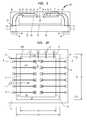
- FIG. 1is a sectional view illustrating a microelectronic assembly 100 including microelectronic device 10 and a conductive plane 60 electrically connected with the interconnection element 30 .
- FIG. 1Ais a plan view from above the surface 28 and looking towards the surface towards contacts 12 .
- the conductive plane 60can include openings 64 which expose individual ones of the contacts 12 .
- the conductive plane 60can include one or more larger openings 64 ′ which expose some or all of the contacts of the microelectronic device.
- microelectronic assembly 100includes a microelectronic device 10 that is bonded the interconnection element by use of a bonding material, such as a dielectric adhesive 53 .
- the microelectronic devicemay be further conductively connected to interconnection element 30 through a first plurality of device wires 65 and also conductively connected to a conductive plane 60 through a second plurality of reference wires 68 .
- Microelectronic device 10can be a single “bare”, i.e., unpackaged die, e.g., a semiconductor chip having microelectronic circuitry thereon.
- microelectronic device 10can include a packaged semiconductor die.
- a plurality of contacts 12are exposed at a surface 28 of the microelectronic device 10 .
- a plurality of contacts 12can be exposed at a contact-bearing surface of a semiconductor die and may be arranged in one or more rows exposed at such surface.
- directionsare stated in this disclosure with reference to a “top”, i.e., contact-bearing surface 28 of a semiconductor chip or microelectronic device 10 .
- directions referred to as “upward” or “rising from”shall refer to the direction orthogonal and away from the microelectronic device top surface 28 .
- Directions referred to as “downward”shall refer to the directions orthogonal to the device top surface 128 and opposite the upward direction.
- a “vertical” directionshall refer to a direction orthogonal to the chip top surface.
- the term “above” a reference pointshall refer to a point upward of the reference point, and the term “below” a reference point shall refer to a point downward of the reference point.
- topof any individual element shall refer to the point or points of that element which extend furthest in the upward direction
- bottomof any element shall refer to the point or points of that element which extend furthest in the downward direction.
- wires 65 , 68typically are not insulated. As seen in FIG. 1 , typically such wires 65 , 68 are bonded to microelectronic device 10 , conductive plane 60 , and to interconnection element 30 using conventional wirebonding techniques. In one embodiment, wires 65 , 68 may be typical of the types of wires used in a conventional wirebonding process. For example, wires 65 , 68 may consist essentially of copper, gold, a gold-silver alloy, or some other metal or alloy of a metal with one or more other metals or materials or an alloy of a metal with one or more other metals and one or more other materials.
- Wirebondswhich may also be referred to herein as “bond wires”, can be formed with relatively precise placement and within desirable tolerances such that parallel, closely spaced runs can be achieved which run parallel to the surface 28 of the conductive plane 60 .
- paralleldenotes a structure which is parallel to another structure within manufacturing tolerances.
- K&SKulicke and Soffa
- device wires 65can be formed which have runs which are perfectly straight in lateral directions above the chip surface 28 and conductive plane 60 or are close to being straight. While such precision can be achieved in forming the wirebonds, nothing is meant to require precisely formed parallel, straight wirebonds other than as specifically recited in the appended claims.
- the conductive plane 60overlies the microelectronic device 10 and may be positioned between the microelectronic device 10 and wires 65 .
- the conductive plane 60can be formed and attached to the microelectronic device 10 by any means known in the art.
- the conductive planemay be laminated onto the surface of the microelectronic device 10 .
- the conductive plane 60can be provided by pre-processing a metal sheet such as a copper foil, for example, to form openings 64 in the metal sheet. Then, the metal sheet can be bonded to the surface 28 of the microelectronic device, such as by using an adhesive 62 .
- microelectronic device 10may also be formed and attached to the surface of the microelectronic device by processing applied to the surface of a microelectronic device 10 such as a metal deposition or plating process applied to the device while the device is in form of a wafer or panel containing a plurality of connected devices or after the device has been singulated from other such devices.
- processing applied to the surface of a microelectronic device 10such as a metal deposition or plating process applied to the device while the device is in form of a wafer or panel containing a plurality of connected devices or after the device has been singulated from other such devices.
- dimensions of the conductive plane 60 in directions oriented horizontally with respect to the surface 28 of microelectronic device 10can be smaller than corresponding dimensions of the microelectronic device surface 28 .
- the surface 28 of the microelectronic devicehas a first dimension 26 extending in a first direction and has a second dimension 34 extending in a second direction that is transverse to the first direction.
- the first and second directionsextend horizontally with respect to the microelectronic device surface 28 , that is, in directions along such surface.
- the conductive layer 60can have a dimension 26 in the first direction which is smaller than the corresponding first dimension 24 of the microelectronic device surface 28 .
- the conductive layer 60can have a dimension 36 in the second direction which is smaller than the corresponding second dimension 34 of the microelectronic device surface 28 .
- a first set of wire bonds 65connect the contacts 12 of the microelectronic device 10 with contacts 75 on the interconnection element 30 .
- the device wires 65have portions which are raised above the surface 28 of the conductive plane 60 . These portions of the device wire 65 can extend in a horizontal direction parallel to or at least generally parallel to the surface of the conductive plane 60 , as shown in FIG. 1 . The portions may be parallel within manufacturing tolerances therefor.
- substantial portions x ( FIG. 1 ) of each of the respective wire bondsare disposed at a substantially uniform distance or height y ( FIG. 1 ) from the conductive plane 60 .
- the height of the wirebonds from the conductive planeis set to between about 50 micrometers from the surface 28 of the microelectronic element and about 100 micrometers from the surface 28 .
- the height from the conductive plane at which the device wires extendcan be selected to achieve desired impedance for carrying signals on the device wires. As discussed below relative to FIG. 1C , the height can be selected is based on a combination of factors such as the thickness of each wire, and the permeability of the dielectric material between the wire and the conductive plane.
- signals to and from the microelectronic devicemay be transmitted with less noise entering the connections (e.g., wirebonds) carrying the signals.
- Each wirebond and the conductive planebeing tied to a source of reference voltage, forms a transmission line structure that has a desired characteristic impedance.
- parameterscan be selected such as the conductive properties of the metal used in the wire, as well as the shape and thickness of the wire, the thickness of the insulating material 50 between the wire and the conductive layer 60 , the dielectric constant of the insulating material, i.e., permeability.
- FIG. 1Cgraphs characteristic impedance Z 0 , in ohms, versus separation distance, in inches, between a signal conductor or conductive element, e.g., a wire of cylindrical cross-section or a trace, and a reference conductor or conductive element, e.g., “ground plane.”
- the reference conductoris assumed to be a planar structure that is large in comparison with the diameter of the signal conductor.
- FIG. 1Bplots characteristic impedance for two different diameter wires. The plots in FIG. 1B can be derived from an equation that governs characteristic impedance in an arrangement having the present geometry. In such equation, the characteristic impedance Z 0 is given by
- Z 0138 ⁇ log ⁇ ( 4 ⁇ H / d ) ⁇ R ⁇ ohms , where H is the separation distance between the wire and the conductive plane, d is the diameter of the wire and ⁇ R is the permeability of the dielectric material that separates the wire from the conductive plane.
- the permeability ⁇ Rcan vary depending on the type of dielectric material used.
- the separation distance His a factor which can be at least partly determined by the process used to fabricate the microelectronic assembly.
- the wire diametermay be at least partly determined by the process used to fabricate the microelectronic assembly.
- the lower curve 320plots the characteristic impedance when the wire used to form a wirebond has a thickness of 1 mil, i.e., 0.001 inch.
- the upper curveplots 322 the characteristic impedance when the wire used to form the wirebond has a thickness of 0.7 mil, i.e., 0.0007 inch.
- characteristic impedances lower than about 70 ohmsare provided when a separation distance H between the wire and the conductive plane is less than or equal to about 0.002 inch (2 mils), i.e., about 50 microns.
- At least one reference wirebond 68directly connects the conductive plane 60 to a reference contact 77 on the interconnection element.
- the reference wires 68are connected to the conductive plane 60 at a point adjacent the outer edge 57 of the conductive plane 60 .
- At least one of the reference wires 68connects the surface conductor 60 with a source of reference potential (not shown).
- At least one reference wire 68 Amay extend directly from the top surface 14 of the conductive plane 60 and extend in a direction transverse to the direction of the device wires 65 connecting the device contacts 12 with the contacts 75 on the interconnection element 30 .
- one or more reference wires 68 B, 68 Cmay extend in a direction parallel to the device wires 65 that connect the device contacts 12 with contacts 75 on the interconnection element 30 .
- at least one reference wire 68 Cmay be positioned between two of the device wires 65 .
- the reference wire 68 Bmay only be adjacent one device wire 65 , such as adjacent one corner of the conductive plane 60 and a corner of microelectronic device 10 , where two adjacent edges of the conductive plane 60 meet, and two edges of the microelectronic device 10 meet. It is to be appreciated that any of the foregoing arrangements alone or in combination with one another, as well as any other arrangement of a reference wire 68 extending from the conductive plane 60 , may be used to provide an electrical connection between the conductive plane 60 and a reference contact 77 , a source of reference potential (not shown), or some other conductive contact or region that is internal or external to the microelectronic assembly 100 .
- a dielectric material 50can be formed to cover and protect the wires 65 , 68 .
- the dielectric 50in this case might be one of a number of different materials such as a polymer, e.g., an epoxy, or another dielectric material, etc.
- dielectric material 50fills the entire void between the wires 65 , 68 and the surfaces of the interconnection element 30 and microelectronic device 10 .
- terminals 40 of the microelectronic assembly 100may be used to connect the microelectronic assembly 100 to a circuit board or external device (not shown), such as through solder balls 42 , which can be attached to the terminals 40 and extend away from a surface 52 of the interconnection element 30 remote from a surface 33 above which microelectronic device 10 is mounted.
- Terminalscan be provided which have other forms than that depicted in FIG. 1 , and can be or include, for example, substantially rigid conductive posts such as formed by etching or plating a metal layer, e.g., copper, or a combination of etching and plating steps.
- the terminalscan be in form of any other known terminal structures which are capable of being used in microelectronic packages or assemblies for electrically connecting such packages or assemblies to a circuit panel, test board or the like.
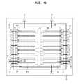
- the conductive layer 60can be provided in the form of multiple planes overlying the microelectronic device 10 .
- the conductive plane 60may be divided into four conductive plane portions 102 , 104 , 106 , 108 .
- device contacts 12may extend between the conductive plane portions 102 , 104 and conductive plane portions 106 , 108 .
- each of the conductive plane portions 102 , 104 , 106 , 108is electrically insulated from one another.
- device wires 65may extend between the device contact 12 and element contacts 77 on the interconnection element 12 .
- reference wires 68may extend as wirebonds from any of the conductive plane portions 102 , 104 , 106 , 108 to another device or contact internal or external to the microelectronic assembly 200 .
- reference wires 68 Emay extend between two conductive plane portions to help ensure that both conductive plane portions remain at a stable voltage despite temporary fluctuations in power demand or other transient effects.
- reference wire 68 Eelectrically connects conductive plane portion 102 and conductive plane portion 104
- reference wire 68 Eelectrically connects conductive plane portions 106 , 108 .
- Reference wires 68 Fmay also electrically connect conductive plane portions 102 , 104 , 106 , 108 to respective reference contacts 77 on the interconnection element 30 .
- One or more reference wires 68 Gmay also extend between any of the conductive plane portions to a device contact 12 .
- a reference wireelectrically connects a conductive plane portion 104 with a reference contact 77
- multiple reference wires 68 Gmay extend between a conductive plane portion (e.g., conductive plane portion 104 , as shown) and a single device contact 12 .
- conductive plane portions 102 , 104are ground planes and conductive plane portions 106 , 108 are power planes.
- the conductive plane portions 102 , 104 which are ground planesmay be electrically connected to device contacts 12 serving as a ground reference therefor, and a ground reference contact 77 of the substrate, and to one another. Further connection of the ground planes 102 , 104 to a reference potential such as a system ground reference can be provided through terminals 40 of the microelectronic assembly 100 ( FIG. 1 ).
- the conductive plane portions 102 , 104 which are power planesmay be electrically connected to particular device contacts 12 of the microelectronic device to which a voltage input other than ground is required, such as for connecting a power supply input.
- the power planescan also be electrically connected with one or more corresponding reference contacts 77 on the interconnection element and to one another. Further connection of the power planes 106 , 108 to a reference potential such as a power supply can be provided through terminals 40 of the microelectronic assembly 100 ( FIG. 1 ). Alternatively, instead of providing ground planes and power planes, all four conductive plane portions 102 , 104 , 106 , and 108 may serve as ground plane portions and be connected to ground device contacts 12 and ground reference contacts 77 .
- the conductive plane 60may be in the form of a plurality of conductive strips 80 which extend along the surface of the microelectronic device 10 in directions parallel to runs of the device wire 65 between the device contacts 12 and the contacts 75 of the interconnection element 30 .
- the conductive strips 80can be mechanically supported or held together with supporting portions 82 .
- the conductive strips and supporting portionsare formed as a metallic structure by subtractively patterning a copper foil or sheet and bonding the remaining metallic structure to the surface 128 of the microelectronic device, such as with an adhesive material 62 .
- the conductive strips 80are divided into two primary portions, a first upper portion 300 and a second lower portion 302 . As shown, there are no supporting portions 82 extending between the first upper portion 300 and second lower portion 302 , such that there is a natural division between the first upper portion 300 and second lower portion 302 .
- reference wires 68 Emay extend between two conductive strips 80 in the first upper portion 300 . Additionally, a reference wire 68 F may extend from the conductive plane 80 in the first upper portion 300 to a reference contact 77 on the interconnection element 30 .
- reference wires 68 Emay extend between two conductive strips 80 in the second lower portion 302 , as well as extend from the conductive strip 80 in the second lower portion 302 to a reference contact 77 on the interconnection element 30 .
- a reference wire 68 Gmay extend from one of the conductive strips 82 to a contact 12 on the microelectronic device 10 .
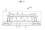
- FIG. 4a sectional view is shown illustrating a microelectronic assembly 400 including microelectronic device 10 and conductive plane 60 electrically connected to an interconnection element 30 .
- FIG. 4Ais a plan view from above the top surface 414 of the conductive plane 60 and looking toward the surface of the conductive plane 60 .
- the conductive plane 60is a continuous sheet of conductive material that overlies the top surface 28 of the microelectronic device 10 .
- the conductive plane 60may be comprised of materials as previously disclosed herein.
- the microelectronic device 10may be bonded to the interconnection element 30 using known bonding materials, such as a dielectric adhesive 53 .
- the conductive plane 60may be directly attached or bonded to the microelectronic element 10 through a lamination process or other known processes, as previously described.
- the conductive plane 60is positioned to overlie the microelectronic device 10 , as well as redistribution traces 404 extending along the surface of the microelectronic device 10 .
- the redistribution traces 404may be formed on the microelectronic device 10 by any suitable metal deposition technique.
- the redistribution traces 404may be formed by depositing a primary metal layer, e.g., by sputtering, electroless deposition, etc. The primary metal layer can then be photolithographically patterned into separate traces 404 , followed by electroplating to increase the thickness of the traces and if desired, form redistribution traces 404 having multiple different metal layers.
- the redistribution traces 404may be formed from a metal layer deposited on the surface of the microelectronic device 10 , which can then be selectively patterned using a subtractive process, such as etching. It is to be appreciated that it is preferable for the formation of the redistribution traces 404 to occur while the microelectronic device 10 is in its wafer form.
- Device contacts 12are positioned along a central portion of the microelectronic device 10 .
- the redistribution contacts 402are exposed between peripheral edges 410 of the microelectronic device 10 and the outer edge 412 of the conductive plane 60 .
- the redistribution traces 404 on the microelectronic device 10provide an electrical connection between the redistribution contacts 402 and the device contacts 12 .
- Device wires 65extend beyond the edge of the microelectronic device 10 to further electrically connect the redistribution contacts 402 with element contacts 75 on the interconnection element 30 . This provides for an electrical connection between the microelectronic device 10 and the interconnection element without requiring substantial lengths of the wires to extend across the top surface 414 of the conductive plane 60 , as disclosed in the previous embodiments.
- substantial lengths of the redistribution traces 404extend between and substantially parallel to the microelectronic device 10 and conductive plane 60 .
- the conductive plane 60is a fixed height above the conductive traces (and the conductive traces 404 a fixed height below the conductive plane 60 )
- a desired impedancecan be obtained from this arrangement, based on the principles previously explained herein.
- Reference wires 68may extend from the conductive plane 60 to reference contacts 77 on the interconnection element 30 .
- the reference wires 68may be further connected to a source of reference potential such as ground or a power supply input terminal of the microelectronic assembly 400 .
- the conductive plane 60may include multiple conductive plane portions 410 , 412 , 414 , 416 overlying the redistribution traces 402 and microelectronic device.
- the device contacts 12respectively extend between conductive plane portion 410 and conductive plane portion 412 , as well as between conductive plane portion 414 and conductive plane portion 416 .
- Redistribution traces 404extend substantially parallel to the conductive plane portions 410 , 412 , 414 , 416 and microelectronic device 10 . Since the substantial lengths of the redistribution traces 404 extend a substantially constant distance from the conductive plane portions 410 , 412 , 414 , and 416 , a desired impedance can be obtained in accordance with previously discussed principles.
- the conductive plane portions 410 , 412may be ground planes and the conductive plane portions 414 , 416 may be power planes.
- at least one reference wire 68 Fcan extend from the ground conductive plane portions 410 , 412 to a reference contact 77 on the interconnection element 30 .
- Another reference wire 68 F′can also extend from the power plane portions 414 , 416 to a reference contact 77 on the interconnection element 30 .
- At least one reference wire 68 Ecan extend between the two conductive plane portions.
- reference wire 68 Eelectrically connects the ground conductive plane portion 410 and ground conductive plane portion 412 .
- reference wire 68 Eelectrically connects the ground conductive plane portion 410 and ground conductive plane portion 412 .
- at least one reference wire 68 Gcan connect a conductive plane portion 414 or 412 , with a contact 12 on the microelectronic device. It is to be appreciated that any combination of the foregoing may be utilized in connection with the present embodiments.
- an encapsulant 491can be deposited around the microelectronic device 10 , conductive plane 60 , and wires 65 , 68 .
- the microelectronic assembly 400can then be connected via terminals 40 , such as conductive pins or solder ball connections, to the contacts 489 of a circuit board 493 or other external device.
- a microelectronic assembly 400 ′according to a further embodiment is shown.
- a second microelectronic device 10 ′ and second conductive plane 60 ′are added in a stacked arrangement to the microelectronic assembly 400 shown in FIG. 4 .
- a spacer 490may be positioned over the first conductive plane 414 to provide a support for the second microelectronic device 10 ′ and second conductive plane 60 ′.
- the spacer 490has a height needed to provide enough clearance for the wires 65 , 68 to extend from the first microelectronic device 10 and first conductive plane 60 to the reference contacts 77 and signal contacts 75 , without contacting a surface of the second microelectronic device 10 ′.
- the second microelectronic device 10 ′ and second conductive plane 60 ′are electrically connected to the interconnection element 30 in the same arrangement as the first microelectronic assembly 400 shown in FIG. 4 .
- Redistribution traces 404 ′extending along the top surface 28 ′ of the microelectronic device 10 ′ electrically connect the device contacts 12 on the surface of the microelectronic device 10 ′ with the redistribution contacts 402 ′ also exposed thereat.
- Signal wires 65 ′extend from the redistribution contacts 402 ′ to signal contacts 75 on the interconnection element.
- reference wires 68 ′extend from the conductive plane 60 ′ to reference contacts 77 on the interconnection element 30 .
- the wires 65 ′, 68 ′ extending from the redistribution contacts on the microelectronic device and the conductive planeextend to contacts positioned adjacent the device and reference contacts 75 , 77 to which the lower assembly 400 is electrically connected.
- a dielectric material 491 ′such as an encapsulant or an overmold can cover and protect the bond wires 65 , 68 and the bond wires 65 ′ 68 ′ extending from the microelectronic devices, and can cover and protect other components within the package such as the microelectronic devices and the conductive planes 60 , 60 ′.
- a system 900 in accordance with a further embodiment of the inventionincludes a structure 906 as described in the prior embodiments of microelectronic assemblies above in conjunction with other electronic components 908 and 910 .
- component 908is a semiconductor chip
- component 910is a display screen, but any other components can be used.
- the systemmay include any number of such components.
- the structure 906 as described abovemay be, for example, a composite chip or a structure incorporating plural chips. In a further variant, both may be provided, and any number of such structures may be used.
- Structure 906 and components 908 and 910are mounted in a common housing 901 , schematically depicted in broken lines, and are electrically interconnected with one another as necessary to form the desired circuit.
- the systemincludes a circuit panel 902 such as a flexible printed circuit board, and the circuit panel includes numerous conductors 904 , of which only one is depicted in FIG. 5 , interconnecting the components with one another.
- the housing 901is depicted as a portable housing of the type usable, for example, in a cellular telephone or personal digital assistant, and screen 910 is exposed at the surface of the housing.
- structure 906includes a light-sensitive element such as an imaging chip
- a lens 911 or other optical devicealso may be provided for routing light to the structure.
- FIG. 24the simplified system shown in FIG. 24 is merely exemplary; other systems, including systems commonly regarded as fixed structures, such as desktop computers, routers and the like can be made using the structures discussed above.
Landscapes
- Engineering & Computer Science (AREA)
- Microelectronics & Electronic Packaging (AREA)
- Power Engineering (AREA)
- Computer Hardware Design (AREA)
- Physics & Mathematics (AREA)
- Condensed Matter Physics & Semiconductors (AREA)
- General Physics & Mathematics (AREA)
- Health & Medical Sciences (AREA)
- Electromagnetism (AREA)
- Toxicology (AREA)
- Semiconductor Integrated Circuits (AREA)
Abstract
Description
where H is the separation distance between the wire and the conductive plane, d is the diameter of the wire and ∈Ris the permeability of the dielectric material that separates the wire from the conductive plane. The permeability ∈Rcan vary depending on the type of dielectric material used. The separation distance H is a factor which can be at least partly determined by the process used to fabricate the microelectronic assembly. The wire diameter may be at least partly determined by the process used to fabricate the microelectronic assembly.
Claims (19)
Priority Applications (1)
| Application Number | Priority Date | Filing Date | Title |
|---|---|---|---|
| US14/306,947US8981579B2 (en) | 2010-09-16 | 2014-06-17 | Impedance controlled packages with metal sheet or 2-layer rdl |
Applications Claiming Priority (2)
| Application Number | Priority Date | Filing Date | Title |
|---|---|---|---|
| US12/883,821US8786083B2 (en) | 2010-09-16 | 2010-09-16 | Impedance controlled packages with metal sheet or 2-layer RDL |
| US14/306,947US8981579B2 (en) | 2010-09-16 | 2014-06-17 | Impedance controlled packages with metal sheet or 2-layer rdl |
Related Parent Applications (1)
| Application Number | Title | Priority Date | Filing Date |
|---|---|---|---|
| US12/883,821DivisionUS8786083B2 (en) | 2010-09-16 | 2010-09-16 | Impedance controlled packages with metal sheet or 2-layer RDL |
Publications (2)
| Publication Number | Publication Date |
|---|---|
| US20140291871A1 US20140291871A1 (en) | 2014-10-02 |
| US8981579B2true US8981579B2 (en) | 2015-03-17 |
Family
ID=45817015
Family Applications (2)
| Application Number | Title | Priority Date | Filing Date |
|---|---|---|---|
| US12/883,821Expired - Fee RelatedUS8786083B2 (en) | 2010-09-16 | 2010-09-16 | Impedance controlled packages with metal sheet or 2-layer RDL |
| US14/306,947Expired - Fee RelatedUS8981579B2 (en) | 2010-09-16 | 2014-06-17 | Impedance controlled packages with metal sheet or 2-layer rdl |
Family Applications Before (1)
| Application Number | Title | Priority Date | Filing Date |
|---|---|---|---|
| US12/883,821Expired - Fee RelatedUS8786083B2 (en) | 2010-09-16 | 2010-09-16 | Impedance controlled packages with metal sheet or 2-layer RDL |
Country Status (1)
| Country | Link |
|---|---|
| US (2) | US8786083B2 (en) |
Families Citing this family (15)
| Publication number | Priority date | Publication date | Assignee | Title |
|---|---|---|---|---|
| KR100950511B1 (en) | 2009-09-22 | 2010-03-30 | 테세라 리써치 엘엘씨 | Microelectronic assembly with impedance controlled wirebond and conductive reference element |
| KR100935854B1 (en) | 2009-09-22 | 2010-01-08 | 테세라 리써치 엘엘씨 | Microelectronic assembly with impedance controlled wirebond and reference wirebond |
| US8581377B2 (en) | 2010-09-16 | 2013-11-12 | Tessera, Inc. | TSOP with impedance control |
| US9136197B2 (en) | 2010-09-16 | 2015-09-15 | Tessera, Inc. | Impedence controlled packages with metal sheet or 2-layer RDL |
| US8853708B2 (en) | 2010-09-16 | 2014-10-07 | Tessera, Inc. | Stacked multi-die packages with impedance control |
| US8786083B2 (en) | 2010-09-16 | 2014-07-22 | Tessera, Inc. | Impedance controlled packages with metal sheet or 2-layer RDL |
| JP5968713B2 (en) | 2012-07-30 | 2016-08-10 | ルネサスエレクトロニクス株式会社 | Semiconductor device |
| JP2016192447A (en)* | 2015-03-30 | 2016-11-10 | 株式会社東芝 | Semiconductor device |
| EP3093990B1 (en)* | 2015-05-13 | 2018-08-15 | Ampleon Netherlands B.V. | Guard bond wires in an integrated circuit package |
| TWI582919B (en)* | 2015-12-31 | 2017-05-11 | 力成科技股份有限公司 | Substrateless fan-out multi-chip package and its fabricating method |
| CN111816636B (en)* | 2019-04-10 | 2022-05-31 | 欣兴电子股份有限公司 | Package carrier board and package structure |
| US11355450B2 (en)* | 2019-08-01 | 2022-06-07 | Mediatek Inc. | Semiconductor package with EMI shielding structure |
| DE102019121894B4 (en)* | 2019-08-14 | 2023-07-06 | Infineon Technologies Ag | Package with integrated multi-tap impedance structure and method for making such a package |
| WO2021039325A1 (en)* | 2019-08-23 | 2021-03-04 | 株式会社村田製作所 | Module |
| US20210118838A1 (en)* | 2019-10-16 | 2021-04-22 | Nanya Technology Corporation | Chip-package device |
Citations (89)
| Publication number | Priority date | Publication date | Assignee | Title |
|---|---|---|---|---|
| US4680613A (en) | 1983-12-01 | 1987-07-14 | Fairchild Semiconductor Corporation | Low impedance package for integrated circuit die |
| US4980753A (en) | 1988-11-21 | 1990-12-25 | Honeywell Inc. | Low-cost high-performance semiconductor chip package |
| US5028983A (en) | 1988-10-28 | 1991-07-02 | International Business Machines Corporation | Multilevel integrated circuit packaging structures |
| US5065282A (en) | 1986-10-17 | 1991-11-12 | Polonio John D | Interconnection mechanisms for electronic components |
| US5343074A (en) | 1993-10-04 | 1994-08-30 | Motorola, Inc. | Semiconductor device having voltage distribution ring(s) and method for making the same |
| JPH06268100A (en) | 1993-03-12 | 1994-09-22 | Nippon Telegr & Teleph Corp <Ntt> | Semiconductor device sealing structure and sealing method |
| US5394010A (en) | 1991-03-13 | 1995-02-28 | Kabushiki Kaisha Toshiba | Semiconductor assembly having laminated semiconductor devices |
| JPH0758138A (en) | 1993-08-16 | 1995-03-03 | Nec Corp | Structure and method for wire bonding |
| US5468999A (en) | 1994-05-26 | 1995-11-21 | Motorola, Inc. | Liquid encapsulated ball grid array semiconductor device with fine pitch wire bonding |
| US5471151A (en) | 1990-02-14 | 1995-11-28 | Particle Interconnect, Inc. | Electrical interconnect using particle enhanced joining of metal surfaces |
| US5523621A (en) | 1994-05-15 | 1996-06-04 | Kabushiki Kaisha Toshiba | Semiconductor device having a multilayer ceramic wiring substrate |
| US5552631A (en) | 1992-06-04 | 1996-09-03 | Lsi Logic Corporation | Semiconductor device assembly including power or ground plane which is provided on opposite surface of insulating layer from signal traces, and is exposed to central opening in insulating layer for interconnection to semiconductor die |
| JPH0927512A (en) | 1995-07-10 | 1997-01-28 | Mitsubishi Electric Corp | Semiconductor device |
| US5606196A (en) | 1995-10-14 | 1997-02-25 | Samsung Electronics Co., Ltd. | High-frequency, high-density semiconductor chip package with screening bonding wires |
| US5639989A (en) | 1994-04-19 | 1997-06-17 | Motorola Inc. | Shielded electronic component assembly and method for making the same |
| US5835988A (en) | 1996-03-27 | 1998-11-10 | Mitsubishi Denki Kabushiki Kaisha | Packed semiconductor device with wrap around external leads |
| US5880403A (en) | 1994-04-01 | 1999-03-09 | Space Electronics, Inc. | Radiation shielding of three dimensional multi-chip modules |
| EP0915504A1 (en) | 1994-04-28 | 1999-05-12 | Fujitsu Limited | Semiconductor package and method of forming the same |
| US6001671A (en) | 1996-04-18 | 1999-12-14 | Tessera, Inc. | Methods for manufacturing a semiconductor package having a sacrificial layer |
| JP2000021926A (en) | 1998-07-06 | 2000-01-21 | Hitachi Ltd | Semiconductor device |
| KR100270817B1 (en) | 1997-05-22 | 2000-11-01 | 이해영 | Package for high speed and high frequency device |
| JP2000332160A (en) | 1999-05-24 | 2000-11-30 | Sumitomo Metal Electronics Devices Inc | Cavity down type semiconductor package |
| JP2001007140A (en) | 1999-04-23 | 2001-01-12 | Sharp Corp | High frequency semiconductor device |
| US6326678B1 (en) | 1993-09-03 | 2001-12-04 | Asat, Limited | Molded plastic package with heat sink and enhanced electrical performance |
| JP2001339016A (en) | 2000-05-30 | 2001-12-07 | Alps Electric Co Ltd | Surface mounting electronic circuit unit |
| US6445594B1 (en) | 2000-02-10 | 2002-09-03 | Mitsubishi Denki Kabushiki Kaisha | Semiconductor device having stacked semiconductor elements |
| US6476506B1 (en) | 2001-09-28 | 2002-11-05 | Motorola, Inc. | Packaged semiconductor with multiple rows of bond pads and method therefor |
| US6518659B1 (en) | 2000-05-08 | 2003-02-11 | Amkor Technology, Inc. | Stackable package having a cavity and a lid for an electronic device |
| US6538336B1 (en) | 2000-11-14 | 2003-03-25 | Rambus Inc. | Wirebond assembly for high-speed integrated circuits |
| US6552417B2 (en) | 1993-09-03 | 2003-04-22 | Asat, Limited | Molded plastic package with heat sink and enhanced electrical performance |
| US20030090001A1 (en) | 2001-11-13 | 2003-05-15 | Kulicke And Soffa Investments, Inc. | Wirebonded semiconductor package structure and method of manufacture |
| US6667546B2 (en) | 2001-11-15 | 2003-12-23 | Siliconware Precision Industries Co., Ltd. | Ball grid array semiconductor package and substrate without power ring or ground ring |
| JP2004112143A (en) | 2002-09-17 | 2004-04-08 | Sumitomo Metal Electronics Devices Inc | Connecting structure of conductor for high frequency signal and semiconductor integrated circuit package |
| US6770822B2 (en) | 2002-02-22 | 2004-08-03 | Bridgewave Communications, Inc. | High frequency device packages and methods |
| US20040164389A1 (en) | 2003-02-25 | 2004-08-26 | I Tseng Lee | [chip package and process for forming the same] |
| US6812580B1 (en) | 2003-06-09 | 2004-11-02 | Freescale Semiconductor, Inc. | Semiconductor package having optimized wire bond positioning |
| US20040238939A1 (en) | 2001-01-04 | 2004-12-02 | Ping Wu | Multi-power ring chip scale package for system level integration |
| KR20050002659A (en) | 2003-06-30 | 2005-01-10 | 엔이씨 가꼬오부쯔 디바이스 가부시끼가이샤 | Hybrid integrated circuit |
| US20050006742A1 (en) | 2002-08-21 | 2005-01-13 | Kabushiki Kaisha Toshiba | High frequency semiconductor module, high frequency semiconductor device and manufacturing method for the same |
| WO2005010989A1 (en) | 2003-07-30 | 2005-02-03 | Koninklijke Philips Electronics, N.V. | Ground arch for wirebond ball grid arrays |
| US20050045378A1 (en) | 2003-08-29 | 2005-03-03 | Heng Mung Suan | Stacked microfeature devices and associated methods |
| US20050098870A1 (en) | 2003-08-27 | 2005-05-12 | Jochen Thomas | FBGA arrangement |
| US20050116013A1 (en) | 2003-11-28 | 2005-06-02 | International Business Machines Corporation | Method and structure for controlled impedance wire bonds using co-dispensing of dielectric spacers |
| US20060049505A1 (en) | 2002-12-10 | 2006-03-09 | Koninklijke Philips Electronics N.V. | High density interconnect power and ground strap and method therefor |
| US20060125079A1 (en) | 2002-12-10 | 2006-06-15 | Chris Wyland | High density package interconnect wire bond strip line and method therefor |
| US20060131742A1 (en) | 2004-12-16 | 2006-06-22 | Fine Tech. Inc. | Packaged chip capable of lowering characteristic impedance |
| US20060145308A1 (en) | 2005-01-05 | 2006-07-06 | International Business Machines Corporation | On-chip circuit pad structure |
| US20060175712A1 (en) | 2005-02-10 | 2006-08-10 | Microbonds, Inc. | High performance IC package and method |
| JP2006216823A (en) | 2005-02-04 | 2006-08-17 | Akita Denshi Systems:Kk | Semiconductor device, its manufacturing method and electronic device |
| US20070007644A1 (en) | 2000-12-22 | 2007-01-11 | Broadcom Corporation | Ball grid array package enhanced with a thermal and electrical connector |
| US7166495B2 (en) | 1996-02-20 | 2007-01-23 | Micron Technology, Inc. | Method of fabricating a multi-die semiconductor package assembly |
| US20070034674A1 (en) | 2003-06-27 | 2007-02-15 | Kabushiki Kaisha Shinkawa | Semiconductor device |
| KR100702970B1 (en) | 2005-07-06 | 2007-04-03 | 삼성전자주식회사 | Semiconductor package having binary connection method and manufacturing method thereof |
| EP1770777A2 (en) | 1998-07-06 | 2007-04-04 | Hitachi, Ltd. | Semiconductor device |
| US7205651B2 (en) | 2004-04-16 | 2007-04-17 | St Assembly Test Services Ltd. | Thermally enhanced stacked die package and fabrication method |
| US20070105272A1 (en) | 2005-08-24 | 2007-05-10 | Micron Technology, Inc. | Microelectronic devices and microelectronic support devices, and associated assemblies and methods |
| US20070170601A1 (en) | 2003-12-26 | 2007-07-26 | Yoshinori Miyaki | Semiconductor device and manufacturing method of them |
| WO2008008948A2 (en) | 2006-07-14 | 2008-01-17 | Texas Instruments Incorporated | System and method of attenuating electromagnetic interference with a grounded top film |
| US20080088012A1 (en) | 2006-08-15 | 2008-04-17 | Yamaha Corporation | Semiconductor device and wire bonding method therefor |
| US20080111248A1 (en) | 2004-12-14 | 2008-05-15 | Chee Seng Foong | Flip Chip And Wire Bond Semiconductor Package |
| US7450110B2 (en) | 2000-01-19 | 2008-11-11 | Immersion Corporation | Haptic input devices |
| US7456505B2 (en) | 2005-07-29 | 2008-11-25 | Infineon Technologies Ag | Integrated circuit chip and integrated device |
| US7466021B2 (en) | 2003-11-17 | 2008-12-16 | Interconnect Portfolio, Llp | Memory packages having stair step interconnection layers |
| US7468560B2 (en) | 2005-01-19 | 2008-12-23 | Infineon Technologies Ag | Semiconductor device with micro connecting elements and method for producing the same |
| US20090057862A1 (en) | 2007-08-31 | 2009-03-05 | Jong-Woo Ha | Integrated circuit package-in-package system with carrier interposer |
| CN101410974A (en) | 2006-03-23 | 2009-04-15 | Nxp股份有限公司 | Enhanced electronic bond wire package |
| US7528011B2 (en) | 1999-02-17 | 2009-05-05 | Sharp Kabushiki Kaisha | Semiconductor device and manufacturing method thereof |
| US7537962B2 (en) | 2006-12-22 | 2009-05-26 | Stats Chippac Ltd. | Method of fabricating a shielded stacked integrated circuit package system |
| US7550842B2 (en)* | 2002-12-12 | 2009-06-23 | Formfactor, Inc. | Integrated circuit assembly |
| US20090256266A1 (en) | 2008-04-10 | 2009-10-15 | Sierra Monolithics, Inc. | Apparatus and method for a chip assembly including a frequency extending device |
| KR100935854B1 (en) | 2009-09-22 | 2010-01-08 | 테세라 리써치 엘엘씨 | Microelectronic assembly with impedance controlled wirebond and reference wirebond |
| WO2010020836A1 (en) | 2008-08-22 | 2010-02-25 | Taiwan Semiconductor Manufacturing Co., Ltd | Impedance controlled electrical interconnection employing meta-materials |
| KR100950511B1 (en) | 2009-09-22 | 2010-03-30 | 테세라 리써치 엘엘씨 | Microelectronic assembly with impedance controlled wirebond and conductive reference element |
| US7723852B1 (en) | 2008-01-21 | 2010-05-25 | Amkor Technology, Inc. | Stacked semiconductor package and method of making same |
| US7727801B2 (en) | 2004-08-27 | 2010-06-01 | Texas Instruments Incorporated | Apparatus for improved power distribution in wirebond semiconductor packages |
| US7768135B1 (en) | 2008-04-17 | 2010-08-03 | Amkor Technology, Inc. | Semiconductor package with fast power-up cycle and method of making same |
| US20100270667A1 (en) | 2009-04-24 | 2010-10-28 | Infineon Technologies Ag | Semiconductor package with multiple chips and substrate in metal cap |
| US7843021B2 (en) | 2008-02-28 | 2010-11-30 | Shandong Gettop Acoustic Co. Ltd. | Double-side mountable MEMS package |
| US7855463B2 (en) | 2006-09-12 | 2010-12-21 | Qimonda Ag | Method for producing a circuit module comprising at least one integrated circuit |
| US7875985B2 (en) | 2006-12-22 | 2011-01-25 | Qimonda Ag | Memory device |
| US8026129B2 (en) | 2006-03-10 | 2011-09-27 | Stats Chippac Ltd. | Stacked integrated circuits package system with passive components |
| US20120068361A1 (en) | 2010-09-16 | 2012-03-22 | Tessera Research Llc | Stacked multi-die packages with impedance control |
| US20120068338A1 (en) | 2010-09-16 | 2012-03-22 | Tessera Research Llc | Impedance controlled packages with metal sheet or 2-layer rdl |
| US20120068317A1 (en) | 2010-09-16 | 2012-03-22 | Tessera Research Llc | Tsop with impedance control |
| US8222725B2 (en) | 2010-09-16 | 2012-07-17 | Tessera, Inc. | Metal can impedance control structure |
| US8237250B2 (en) | 2008-08-21 | 2012-08-07 | Advanced Semiconductor Engineering, Inc. | Advanced quad flat non-leaded package structure and manufacturing method thereof |
| US8243465B2 (en) | 2009-02-18 | 2012-08-14 | Elpida Memory, Inc. | Semiconductor device with additional power supply paths |
| US8253258B2 (en) | 2009-03-30 | 2012-08-28 | Elpida Memory, Inc. | Semiconductor device with hollow and throughhole and method of manufacturing same |
| US8294249B2 (en) | 2008-08-05 | 2012-10-23 | Integrated Device Technology Inc. | Lead frame package |
- 2010
- 2010-09-16USUS12/883,821patent/US8786083B2/ennot_activeExpired - Fee Related
- 2014
- 2014-06-17USUS14/306,947patent/US8981579B2/ennot_activeExpired - Fee Related
Patent Citations (99)
| Publication number | Priority date | Publication date | Assignee | Title |
|---|---|---|---|---|
| US4680613A (en) | 1983-12-01 | 1987-07-14 | Fairchild Semiconductor Corporation | Low impedance package for integrated circuit die |
| US5065282A (en) | 1986-10-17 | 1991-11-12 | Polonio John D | Interconnection mechanisms for electronic components |
| US5028983A (en) | 1988-10-28 | 1991-07-02 | International Business Machines Corporation | Multilevel integrated circuit packaging structures |
| US4980753A (en) | 1988-11-21 | 1990-12-25 | Honeywell Inc. | Low-cost high-performance semiconductor chip package |
| US5471151A (en) | 1990-02-14 | 1995-11-28 | Particle Interconnect, Inc. | Electrical interconnect using particle enhanced joining of metal surfaces |
| US5394010A (en) | 1991-03-13 | 1995-02-28 | Kabushiki Kaisha Toshiba | Semiconductor assembly having laminated semiconductor devices |
| US5552631A (en) | 1992-06-04 | 1996-09-03 | Lsi Logic Corporation | Semiconductor device assembly including power or ground plane which is provided on opposite surface of insulating layer from signal traces, and is exposed to central opening in insulating layer for interconnection to semiconductor die |
| US5638596A (en) | 1992-06-04 | 1997-06-17 | Lsi Logic Corporation | Method of employing multi-layer tab tape in semiconductor device assembly by selecting, breaking, downwardly bending and bonding tab tape trace free ends to a ground or power plane |
| JPH06268100A (en) | 1993-03-12 | 1994-09-22 | Nippon Telegr & Teleph Corp <Ntt> | Semiconductor device sealing structure and sealing method |
| JPH0758138A (en) | 1993-08-16 | 1995-03-03 | Nec Corp | Structure and method for wire bonding |
| US6552417B2 (en) | 1993-09-03 | 2003-04-22 | Asat, Limited | Molded plastic package with heat sink and enhanced electrical performance |
| US6326678B1 (en) | 1993-09-03 | 2001-12-04 | Asat, Limited | Molded plastic package with heat sink and enhanced electrical performance |
| US5343074A (en) | 1993-10-04 | 1994-08-30 | Motorola, Inc. | Semiconductor device having voltage distribution ring(s) and method for making the same |
| US5880403A (en) | 1994-04-01 | 1999-03-09 | Space Electronics, Inc. | Radiation shielding of three dimensional multi-chip modules |
| US5639989A (en) | 1994-04-19 | 1997-06-17 | Motorola Inc. | Shielded electronic component assembly and method for making the same |
| EP0915504A1 (en) | 1994-04-28 | 1999-05-12 | Fujitsu Limited | Semiconductor package and method of forming the same |
| US5523621A (en) | 1994-05-15 | 1996-06-04 | Kabushiki Kaisha Toshiba | Semiconductor device having a multilayer ceramic wiring substrate |
| US5468999A (en) | 1994-05-26 | 1995-11-21 | Motorola, Inc. | Liquid encapsulated ball grid array semiconductor device with fine pitch wire bonding |
| JPH0927512A (en) | 1995-07-10 | 1997-01-28 | Mitsubishi Electric Corp | Semiconductor device |
| US5606196A (en) | 1995-10-14 | 1997-02-25 | Samsung Electronics Co., Ltd. | High-frequency, high-density semiconductor chip package with screening bonding wires |
| US7166495B2 (en) | 1996-02-20 | 2007-01-23 | Micron Technology, Inc. | Method of fabricating a multi-die semiconductor package assembly |
| US5835988A (en) | 1996-03-27 | 1998-11-10 | Mitsubishi Denki Kabushiki Kaisha | Packed semiconductor device with wrap around external leads |
| US6001671A (en) | 1996-04-18 | 1999-12-14 | Tessera, Inc. | Methods for manufacturing a semiconductor package having a sacrificial layer |
| KR100270817B1 (en) | 1997-05-22 | 2000-11-01 | 이해영 | Package for high speed and high frequency device |
| US20010015490A1 (en) | 1997-05-22 | 2001-08-23 | Hai Young Lee | High speed digital and microwave device package |
| JP2000021926A (en) | 1998-07-06 | 2000-01-21 | Hitachi Ltd | Semiconductor device |
| EP1770777A2 (en) | 1998-07-06 | 2007-04-04 | Hitachi, Ltd. | Semiconductor device |
| US7528011B2 (en) | 1999-02-17 | 2009-05-05 | Sharp Kabushiki Kaisha | Semiconductor device and manufacturing method thereof |
| JP2001007140A (en) | 1999-04-23 | 2001-01-12 | Sharp Corp | High frequency semiconductor device |
| JP2000332160A (en) | 1999-05-24 | 2000-11-30 | Sumitomo Metal Electronics Devices Inc | Cavity down type semiconductor package |
| US7450110B2 (en) | 2000-01-19 | 2008-11-11 | Immersion Corporation | Haptic input devices |
| US6445594B1 (en) | 2000-02-10 | 2002-09-03 | Mitsubishi Denki Kabushiki Kaisha | Semiconductor device having stacked semiconductor elements |
| US6518659B1 (en) | 2000-05-08 | 2003-02-11 | Amkor Technology, Inc. | Stackable package having a cavity and a lid for an electronic device |
| JP2001339016A (en) | 2000-05-30 | 2001-12-07 | Alps Electric Co Ltd | Surface mounting electronic circuit unit |
| US6538336B1 (en) | 2000-11-14 | 2003-03-25 | Rambus Inc. | Wirebond assembly for high-speed integrated circuits |
| US20070007644A1 (en) | 2000-12-22 | 2007-01-11 | Broadcom Corporation | Ball grid array package enhanced with a thermal and electrical connector |
| US20040238939A1 (en) | 2001-01-04 | 2004-12-02 | Ping Wu | Multi-power ring chip scale package for system level integration |
| US6476506B1 (en) | 2001-09-28 | 2002-11-05 | Motorola, Inc. | Packaged semiconductor with multiple rows of bond pads and method therefor |
| US20030090001A1 (en) | 2001-11-13 | 2003-05-15 | Kulicke And Soffa Investments, Inc. | Wirebonded semiconductor package structure and method of manufacture |
| US6667546B2 (en) | 2001-11-15 | 2003-12-23 | Siliconware Precision Industries Co., Ltd. | Ball grid array semiconductor package and substrate without power ring or ground ring |
| US6770822B2 (en) | 2002-02-22 | 2004-08-03 | Bridgewave Communications, Inc. | High frequency device packages and methods |
| US20050006742A1 (en) | 2002-08-21 | 2005-01-13 | Kabushiki Kaisha Toshiba | High frequency semiconductor module, high frequency semiconductor device and manufacturing method for the same |
| JP2004112143A (en) | 2002-09-17 | 2004-04-08 | Sumitomo Metal Electronics Devices Inc | Connecting structure of conductor for high frequency signal and semiconductor integrated circuit package |
| US20060049505A1 (en) | 2002-12-10 | 2006-03-09 | Koninklijke Philips Electronics N.V. | High density interconnect power and ground strap and method therefor |
| US20060125079A1 (en) | 2002-12-10 | 2006-06-15 | Chris Wyland | High density package interconnect wire bond strip line and method therefor |
| US7550842B2 (en)* | 2002-12-12 | 2009-06-23 | Formfactor, Inc. | Integrated circuit assembly |
| US20040164389A1 (en) | 2003-02-25 | 2004-08-26 | I Tseng Lee | [chip package and process for forming the same] |
| US6812580B1 (en) | 2003-06-09 | 2004-11-02 | Freescale Semiconductor, Inc. | Semiconductor package having optimized wire bond positioning |
| US20070034674A1 (en) | 2003-06-27 | 2007-02-15 | Kabushiki Kaisha Shinkawa | Semiconductor device |
| KR20050002659A (en) | 2003-06-30 | 2005-01-10 | 엔이씨 가꼬오부쯔 디바이스 가부시끼가이샤 | Hybrid integrated circuit |
| US20060180916A1 (en) | 2003-07-30 | 2006-08-17 | Koninklijke Philips Electronics N.V. | Ground arch for wirebond ball grid arrays |
| US7217997B2 (en) | 2003-07-30 | 2007-05-15 | Nxp Bv. | Ground arch for wirebond ball grid arrays |
| WO2005010989A1 (en) | 2003-07-30 | 2005-02-03 | Koninklijke Philips Electronics, N.V. | Ground arch for wirebond ball grid arrays |
| US20050098870A1 (en) | 2003-08-27 | 2005-05-12 | Jochen Thomas | FBGA arrangement |
| US20050045378A1 (en) | 2003-08-29 | 2005-03-03 | Heng Mung Suan | Stacked microfeature devices and associated methods |
| US7466021B2 (en) | 2003-11-17 | 2008-12-16 | Interconnect Portfolio, Llp | Memory packages having stair step interconnection layers |
| US7303113B2 (en) | 2003-11-28 | 2007-12-04 | International Business Machines Corporation | Method and structure for controlled impedance wire bonds using co-dispensing of dielectric spacers |
| US20050116013A1 (en) | 2003-11-28 | 2005-06-02 | International Business Machines Corporation | Method and structure for controlled impedance wire bonds using co-dispensing of dielectric spacers |
| US20070170601A1 (en) | 2003-12-26 | 2007-07-26 | Yoshinori Miyaki | Semiconductor device and manufacturing method of them |
| US20070148821A1 (en)* | 2004-04-16 | 2007-06-28 | Byung Tai Do | Thermally enhanced stacked die package and fabrication method |
| US7205651B2 (en) | 2004-04-16 | 2007-04-17 | St Assembly Test Services Ltd. | Thermally enhanced stacked die package and fabrication method |
| US7727801B2 (en) | 2004-08-27 | 2010-06-01 | Texas Instruments Incorporated | Apparatus for improved power distribution in wirebond semiconductor packages |
| US20080111248A1 (en) | 2004-12-14 | 2008-05-15 | Chee Seng Foong | Flip Chip And Wire Bond Semiconductor Package |
| US20060131742A1 (en) | 2004-12-16 | 2006-06-22 | Fine Tech. Inc. | Packaged chip capable of lowering characteristic impedance |
| US20060145308A1 (en) | 2005-01-05 | 2006-07-06 | International Business Machines Corporation | On-chip circuit pad structure |
| US7468560B2 (en) | 2005-01-19 | 2008-12-23 | Infineon Technologies Ag | Semiconductor device with micro connecting elements and method for producing the same |
| JP2006216823A (en) | 2005-02-04 | 2006-08-17 | Akita Denshi Systems:Kk | Semiconductor device, its manufacturing method and electronic device |
| US20060175712A1 (en) | 2005-02-10 | 2006-08-10 | Microbonds, Inc. | High performance IC package and method |
| KR100702970B1 (en) | 2005-07-06 | 2007-04-03 | 삼성전자주식회사 | Semiconductor package having binary connection method and manufacturing method thereof |
| US7456505B2 (en) | 2005-07-29 | 2008-11-25 | Infineon Technologies Ag | Integrated circuit chip and integrated device |
| US20070105272A1 (en) | 2005-08-24 | 2007-05-10 | Micron Technology, Inc. | Microelectronic devices and microelectronic support devices, and associated assemblies and methods |
| US8026129B2 (en) | 2006-03-10 | 2011-09-27 | Stats Chippac Ltd. | Stacked integrated circuits package system with passive components |
| CN101410974A (en) | 2006-03-23 | 2009-04-15 | Nxp股份有限公司 | Enhanced electronic bond wire package |
| WO2008008948A2 (en) | 2006-07-14 | 2008-01-17 | Texas Instruments Incorporated | System and method of attenuating electromagnetic interference with a grounded top film |
| US20080088012A1 (en) | 2006-08-15 | 2008-04-17 | Yamaha Corporation | Semiconductor device and wire bonding method therefor |
| US7855463B2 (en) | 2006-09-12 | 2010-12-21 | Qimonda Ag | Method for producing a circuit module comprising at least one integrated circuit |
| US7537962B2 (en) | 2006-12-22 | 2009-05-26 | Stats Chippac Ltd. | Method of fabricating a shielded stacked integrated circuit package system |
| US7875985B2 (en) | 2006-12-22 | 2011-01-25 | Qimonda Ag | Memory device |
| US20090057862A1 (en) | 2007-08-31 | 2009-03-05 | Jong-Woo Ha | Integrated circuit package-in-package system with carrier interposer |
| US7723852B1 (en) | 2008-01-21 | 2010-05-25 | Amkor Technology, Inc. | Stacked semiconductor package and method of making same |
| US7843021B2 (en) | 2008-02-28 | 2010-11-30 | Shandong Gettop Acoustic Co. Ltd. | Double-side mountable MEMS package |
| US20090256266A1 (en) | 2008-04-10 | 2009-10-15 | Sierra Monolithics, Inc. | Apparatus and method for a chip assembly including a frequency extending device |
| US7768135B1 (en) | 2008-04-17 | 2010-08-03 | Amkor Technology, Inc. | Semiconductor package with fast power-up cycle and method of making same |
| US8294249B2 (en) | 2008-08-05 | 2012-10-23 | Integrated Device Technology Inc. | Lead frame package |
| US8237250B2 (en) | 2008-08-21 | 2012-08-07 | Advanced Semiconductor Engineering, Inc. | Advanced quad flat non-leaded package structure and manufacturing method thereof |
| WO2010020836A1 (en) | 2008-08-22 | 2010-02-25 | Taiwan Semiconductor Manufacturing Co., Ltd | Impedance controlled electrical interconnection employing meta-materials |
| US8243465B2 (en) | 2009-02-18 | 2012-08-14 | Elpida Memory, Inc. | Semiconductor device with additional power supply paths |
| US20100232128A1 (en) | 2009-03-13 | 2010-09-16 | Tessera Research Llc | Microelectronic assembly with impedance controlled wirebond and reference wirebond |
| US7923851B2 (en) | 2009-03-13 | 2011-04-12 | Tessera Research Llc | Microelectronic assembly with impedance controlled wirebond and conductive reference element |
| US20100230828A1 (en) | 2009-03-13 | 2010-09-16 | Tessera Research Llc | Microelectronic assembly with impedance controlled wirebond and conductive reference element |
| US8575766B2 (en)* | 2009-03-13 | 2013-11-05 | Tessera, Inc. | Microelectronic assembly with impedance controlled wirebond and conductive reference element |
| US8253258B2 (en) | 2009-03-30 | 2012-08-28 | Elpida Memory, Inc. | Semiconductor device with hollow and throughhole and method of manufacturing same |
| US20100270667A1 (en) | 2009-04-24 | 2010-10-28 | Infineon Technologies Ag | Semiconductor package with multiple chips and substrate in metal cap |
| KR100935854B1 (en) | 2009-09-22 | 2010-01-08 | 테세라 리써치 엘엘씨 | Microelectronic assembly with impedance controlled wirebond and reference wirebond |
| KR100950511B1 (en) | 2009-09-22 | 2010-03-30 | 테세라 리써치 엘엘씨 | Microelectronic assembly with impedance controlled wirebond and conductive reference element |
| US20120068361A1 (en) | 2010-09-16 | 2012-03-22 | Tessera Research Llc | Stacked multi-die packages with impedance control |
| US20120068338A1 (en) | 2010-09-16 | 2012-03-22 | Tessera Research Llc | Impedance controlled packages with metal sheet or 2-layer rdl |
| US20120068317A1 (en) | 2010-09-16 | 2012-03-22 | Tessera Research Llc | Tsop with impedance control |
| US8222725B2 (en) | 2010-09-16 | 2012-07-17 | Tessera, Inc. | Metal can impedance control structure |
Non-Patent Citations (15)
| Title |
|---|
| Chinese Office Action for Application No. 201080020828.3 dated Jul. 29, 2013. |
| Chinese Office Action for Application No. 201080020828.3 dated Mar. 3, 2014. |
| Chinese Office Action for Application No. 201080020851.2 dated Nov. 28, 2013. |
| International Search Report Application No. PCT/US2010/027135, dated Aug. 30, 2011. |
| International Search Report, PCT/US2010/027141, dated Jan. 6, 2012. |
| Japanese Office Action for Application No. 2011-554232 dated Feb. 4, 2014. |
| Japanese Office Action for Application No. 2011-554234 dated Jul. 12, 2013. |
| Partial International Search Report and Invitation to Pay Additional Fees, PCT/US2010/027135, dated Mar. 21, 2011. |
| Partial International Search Report and Invitation to Pay Additional Fees, PCT/US2010/027141, dated Jan. 27, 2011. |
| Taiwan Office Action for Application No. 099107377 dated Feb. 18, 2013. |
| U.S. Appl. No. 12/883,556. |
| U.S. Appl. No. 12/883,612. |
| U.S. Appl. No. 12/883,811. |
| U.S. Appl. No. 12/883,821, filed Sep. 16, 2010. |
| U.S. Non-Final Office Action for U.S. Appl. No. 13/472,081 dated Nov. 5, 2014. |
Also Published As
| Publication number | Publication date |
|---|---|
| US20140291871A1 (en) | 2014-10-02 |
| US8786083B2 (en) | 2014-07-22 |
| US20120068338A1 (en) | 2012-03-22 |
Similar Documents
| Publication | Publication Date | Title |
|---|---|---|
| US8981579B2 (en) | Impedance controlled packages with metal sheet or 2-layer rdl | |
| US8624407B2 (en) | Microelectronic assembly with impedance controlled wirebond and reference wirebond | |
| US7368813B2 (en) | Semiconductor device including semiconductor element surrounded by an insulating member and wiring structures on upper and lower surfaces of the semiconductor element and insulating member, and manufacturing method thereof | |
| KR101653856B1 (en) | Semiconductor device and manufacturing method thereof | |
| KR100592786B1 (en) | Laminated package and its manufacturing method using surface-mount semiconductor package | |
| KR100626618B1 (en) | Semiconductor chip stack package and manufacturing method | |
| US6483718B2 (en) | Semiconductor device and method of manufacture thereof, circuit board, and electronic instrument | |
| US8994195B2 (en) | Microelectronic assembly with impedance controlled wirebond and conductive reference element | |
| US8853708B2 (en) | Stacked multi-die packages with impedance control | |
| US6995043B2 (en) | Methods for fabricating routing elements for multichip modules | |
| US20050001304A1 (en) | Chip scale package and method of fabricating the same | |
| US20040135243A1 (en) | Semiconductor device, its manufacturing method and electronic device | |
| US9136197B2 (en) | Impedence controlled packages with metal sheet or 2-layer RDL | |
| US8222725B2 (en) | Metal can impedance control structure | |
| US7410827B2 (en) | Semiconductor device and method of fabricating the same, circuit board, and electronic instrument | |
| JP2003273280A (en) | Chip package and its manufacturing method | |
| KR20000072995A (en) | Stack type semiconductor chip package and manufacturing method thereof | |
| JP2006173376A (en) | Semiconductor apparatus and method for manufacturing the same |
Legal Events
| Date | Code | Title | Description |
|---|---|---|---|
| AS | Assignment | Owner name:TESSERA, INC., CALIFORNIA Free format text:ASSIGNMENT OF ASSIGNORS INTEREST;ASSIGNOR:TESSERA RESEARCH LLC;REEL/FRAME:034103/0079 Effective date:20110908 Owner name:TESSERA RESEARCH LLC, CALIFORNIA Free format text:ASSIGNMENT OF ASSIGNORS INTEREST;ASSIGNORS:HABA, BELGACEM;CHAU, ELLIS;ZOHNI, WAEL;AND OTHERS;SIGNING DATES FROM 20100924 TO 20100929;REEL/FRAME:034103/0039 | |
| STCF | Information on status: patent grant | Free format text:PATENTED CASE | |
| AS | Assignment | Owner name:ROYAL BANK OF CANADA, AS COLLATERAL AGENT, CANADA Free format text:SECURITY INTEREST;ASSIGNORS:INVENSAS CORPORATION;TESSERA, INC.;TESSERA ADVANCED TECHNOLOGIES, INC.;AND OTHERS;REEL/FRAME:040797/0001 Effective date:20161201 | |
| FEPP | Fee payment procedure | Free format text:MAINTENANCE FEE REMINDER MAILED (ORIGINAL EVENT CODE: REM.); ENTITY STATUS OF PATENT OWNER: LARGE ENTITY | |
| LAPS | Lapse for failure to pay maintenance fees | Free format text:PATENT EXPIRED FOR FAILURE TO PAY MAINTENANCE FEES (ORIGINAL EVENT CODE: EXP.); ENTITY STATUS OF PATENT OWNER: LARGE ENTITY | |
| STCH | Information on status: patent discontinuation | Free format text:PATENT EXPIRED DUE TO NONPAYMENT OF MAINTENANCE FEES UNDER 37 CFR 1.362 | |
| FP | Lapsed due to failure to pay maintenance fee | Effective date:20190317 | |
| AS | Assignment | Owner name:DTS LLC, CALIFORNIA Free format text:RELEASE BY SECURED PARTY;ASSIGNOR:ROYAL BANK OF CANADA;REEL/FRAME:052920/0001 Effective date:20200601 Owner name:DTS, INC., CALIFORNIA Free format text:RELEASE BY SECURED PARTY;ASSIGNOR:ROYAL BANK OF CANADA;REEL/FRAME:052920/0001 Effective date:20200601 Owner name:TESSERA, INC., CALIFORNIA Free format text:RELEASE BY SECURED PARTY;ASSIGNOR:ROYAL BANK OF CANADA;REEL/FRAME:052920/0001 Effective date:20200601 Owner name:IBIQUITY DIGITAL CORPORATION, MARYLAND Free format text:RELEASE BY SECURED PARTY;ASSIGNOR:ROYAL BANK OF CANADA;REEL/FRAME:052920/0001 Effective date:20200601 Owner name:PHORUS, INC., CALIFORNIA Free format text:RELEASE BY SECURED PARTY;ASSIGNOR:ROYAL BANK OF CANADA;REEL/FRAME:052920/0001 Effective date:20200601 Owner name:FOTONATION CORPORATION (F/K/A DIGITALOPTICS CORPORATION AND F/K/A DIGITALOPTICS CORPORATION MEMS), CALIFORNIA Free format text:RELEASE BY SECURED PARTY;ASSIGNOR:ROYAL BANK OF CANADA;REEL/FRAME:052920/0001 Effective date:20200601 Owner name:TESSERA ADVANCED TECHNOLOGIES, INC, CALIFORNIA Free format text:RELEASE BY SECURED PARTY;ASSIGNOR:ROYAL BANK OF CANADA;REEL/FRAME:052920/0001 Effective date:20200601 Owner name:INVENSAS BONDING TECHNOLOGIES, INC. (F/K/A ZIPTRONIX, INC.), CALIFORNIA Free format text:RELEASE BY SECURED PARTY;ASSIGNOR:ROYAL BANK OF CANADA;REEL/FRAME:052920/0001 Effective date:20200601 Owner name:INVENSAS CORPORATION, CALIFORNIA Free format text:RELEASE BY SECURED PARTY;ASSIGNOR:ROYAL BANK OF CANADA;REEL/FRAME:052920/0001 Effective date:20200601 |