US8981410B1 - Distributed bragg reflector for reflecting light of multiple wavelengths from an LED - Google Patents
Distributed bragg reflector for reflecting light of multiple wavelengths from an LEDDownload PDFInfo
- Publication number
- US8981410B1 US8981410B1US14/055,596US201314055596AUS8981410B1US 8981410 B1US8981410 B1US 8981410B1US 201314055596 AUS201314055596 AUS 201314055596AUS 8981410 B1US8981410 B1US 8981410B1
- Authority
- US
- United States
- Prior art keywords
- light
- layer
- wavelength
- led device
- periods
- Prior art date
- Legal status (The legal status is an assumption and is not a legal conclusion. Google has not performed a legal analysis and makes no representation as to the accuracy of the status listed.)
- Active
Links
- 239000000758substrateSubstances0.000claimsabstractdescription34
- 239000010410layerSubstances0.000claimsdescription111
- VYPSYNLAJGMNEJ-UHFFFAOYSA-NSilicium dioxideChemical compoundO=[Si]=OVYPSYNLAJGMNEJ-UHFFFAOYSA-N0.000claimsdescription22
- 239000000463materialSubstances0.000claimsdescription21
- 229910052751metalInorganic materials0.000claimsdescription17
- 239000002184metalSubstances0.000claimsdescription17
- GWEVSGVZZGPLCZ-UHFFFAOYSA-NTitan oxideChemical compoundO=[Ti]=OGWEVSGVZZGPLCZ-UHFFFAOYSA-N0.000claimsdescription16
- OAICVXFJPJFONN-UHFFFAOYSA-NPhosphorusChemical compound[P]OAICVXFJPJFONN-UHFFFAOYSA-N0.000claimsdescription13
- 239000003989dielectric materialSubstances0.000claimsdescription11
- 239000000377silicon dioxideSubstances0.000claimsdescription11
- 230000003287optical effectEffects0.000claimsdescription7
- 235000012239silicon dioxideNutrition0.000claimsdescription7
- 229910052681coesiteInorganic materials0.000claimsdescription5
- 229910052906cristobaliteInorganic materials0.000claimsdescription5
- 229910052709silverInorganic materials0.000claimsdescription5
- 239000004332silverSubstances0.000claimsdescription5
- 229910052682stishoviteInorganic materials0.000claimsdescription5
- 229910052905tridymiteInorganic materials0.000claimsdescription5
- PXHVJJICTQNCMI-UHFFFAOYSA-NNickelChemical compound[Ni]PXHVJJICTQNCMI-UHFFFAOYSA-N0.000claimsdescription4
- 229910052738indiumInorganic materials0.000claimsdescription4
- APFVFJFRJDLVQX-UHFFFAOYSA-Nindium atomChemical compound[In]APFVFJFRJDLVQX-UHFFFAOYSA-N0.000claimsdescription4
- ZKATWMILCYLAPD-UHFFFAOYSA-Nniobium pentoxideChemical compoundO=[Nb](=O)O[Nb](=O)=OZKATWMILCYLAPD-UHFFFAOYSA-N0.000claimsdescription4
- BASFCYQUMIYNBI-UHFFFAOYSA-NplatinumChemical compound[Pt]BASFCYQUMIYNBI-UHFFFAOYSA-N0.000claimsdescription4
- 238000004064recyclingMethods0.000claimsdescription4
- GYHNNYVSQQEPJS-UHFFFAOYSA-NGalliumChemical compound[Ga]GYHNNYVSQQEPJS-UHFFFAOYSA-N0.000claimsdescription3
- 229910052782aluminiumInorganic materials0.000claimsdescription3
- XAGFODPZIPBFFR-UHFFFAOYSA-NaluminiumChemical compound[Al]XAGFODPZIPBFFR-UHFFFAOYSA-N0.000claimsdescription3
- 229910052733galliumInorganic materials0.000claimsdescription3
- 239000002356single layerSubstances0.000claimsdescription3
- 229910052581Si3N4Inorganic materials0.000claimsdescription2
- BQCADISMDOOEFD-UHFFFAOYSA-NSilverChemical compound[Ag]BQCADISMDOOEFD-UHFFFAOYSA-N0.000claimsdescription2
- WUKWITHWXAAZEY-UHFFFAOYSA-Lcalcium difluorideChemical compound[F-].[F-].[Ca+2]WUKWITHWXAAZEY-UHFFFAOYSA-L0.000claimsdescription2
- 229910001634calcium fluorideInorganic materials0.000claimsdescription2
- 229910001635magnesium fluorideInorganic materials0.000claimsdescription2
- 229910052759nickelInorganic materials0.000claimsdescription2
- 229910052697platinumInorganic materials0.000claimsdescription2
- 229910052703rhodiumInorganic materials0.000claimsdescription2
- 239000010948rhodiumSubstances0.000claimsdescription2
- MHOVAHRLVXNVSD-UHFFFAOYSA-Nrhodium atomChemical compound[Rh]MHOVAHRLVXNVSD-UHFFFAOYSA-N0.000claimsdescription2
- SBIBMFFZSBJNJF-UHFFFAOYSA-Nselenium;zincChemical compound[Se]=[Zn]SBIBMFFZSBJNJF-UHFFFAOYSA-N0.000claimsdescription2
- PBCFLUZVCVVTBY-UHFFFAOYSA-Ntantalum pentoxideInorganic materialsO=[Ta](=O)O[Ta](=O)=OPBCFLUZVCVVTBY-UHFFFAOYSA-N0.000claimsdescription2
- 239000004408titanium dioxideSubstances0.000claims4
- 238000002310reflectometryMethods0.000description23
- 238000010586diagramMethods0.000description13
- 238000001228spectrumMethods0.000description6
- 229910002601GaNInorganic materials0.000description4
- 239000000470constituentSubstances0.000description3
- 238000000034methodMethods0.000description3
- 230000010363phase shiftEffects0.000description3
- 229910052594sapphireInorganic materials0.000description3
- 239000010980sapphireSubstances0.000description3
- 238000004088simulationMethods0.000description3
- IJGRMHOSHXDMSA-UHFFFAOYSA-NAtomic nitrogenChemical compoundN#NIJGRMHOSHXDMSA-UHFFFAOYSA-N0.000description2
- AZDRQVAHHNSJOQ-UHFFFAOYSA-NalumaneChemical group[AlH3]AZDRQVAHHNSJOQ-UHFFFAOYSA-N0.000description2
- 230000008859changeEffects0.000description2
- 230000001427coherent effectEffects0.000description2
- 239000002245particleSubstances0.000description2
- 238000009304pastoral farmingMethods0.000description2
- 229920001296polysiloxanePolymers0.000description2
- ZMHWQAHZKUPENF-UHFFFAOYSA-N1,2-dichloro-3-(4-chlorophenyl)benzeneChemical compoundC1=CC(Cl)=CC=C1C1=CC=CC(Cl)=C1ClZMHWQAHZKUPENF-UHFFFAOYSA-N0.000description1
- 229910017083AlNInorganic materials0.000description1
- JMASRVWKEDWRBT-UHFFFAOYSA-NGallium nitrideChemical compound[Ga]#NJMASRVWKEDWRBT-UHFFFAOYSA-N0.000description1
- 238000010521absorption reactionMethods0.000description1
- 230000006978adaptationEffects0.000description1
- 239000000853adhesiveSubstances0.000description1
- 230000001070adhesive effectEffects0.000description1
- 238000004364calculation methodMethods0.000description1
- 239000002131composite materialSubstances0.000description1
- 238000011109contaminationMethods0.000description1
- 239000008393encapsulating agentSubstances0.000description1
- -1for exampleSubstances0.000description1
- 230000006872improvementEffects0.000description1
- AMGQUBHHOARCQH-UHFFFAOYSA-Nindium;oxotinChemical compound[In].[Sn]=OAMGQUBHHOARCQH-UHFFFAOYSA-N0.000description1
- 230000007246mechanismEffects0.000description1
- 239000000203mixtureSubstances0.000description1
- 238000012986modificationMethods0.000description1
- 230000004048modificationEffects0.000description1
- 229910003465moissaniteInorganic materials0.000description1
- 229910052757nitrogenInorganic materials0.000description1
- 229910010271silicon carbideInorganic materials0.000description1
- 230000003595spectral effectEffects0.000description1
- 239000012780transparent materialSubstances0.000description1
Images


Classifications
- H01L33/46—
- G—PHYSICS
- G02—OPTICS
- G02B—OPTICAL ELEMENTS, SYSTEMS OR APPARATUS
- G02B5/00—Optical elements other than lenses
- G02B5/08—Mirrors
- G02B5/0816—Multilayer mirrors, i.e. having two or more reflecting layers
- G02B5/0825—Multilayer mirrors, i.e. having two or more reflecting layers the reflecting layers comprising dielectric materials only
- G02B5/0833—Multilayer mirrors, i.e. having two or more reflecting layers the reflecting layers comprising dielectric materials only comprising inorganic materials only
- H—ELECTRICITY
- H10—SEMICONDUCTOR DEVICES; ELECTRIC SOLID-STATE DEVICES NOT OTHERWISE PROVIDED FOR
- H10H—INORGANIC LIGHT-EMITTING SEMICONDUCTOR DEVICES HAVING POTENTIAL BARRIERS
- H10H20/00—Individual inorganic light-emitting semiconductor devices having potential barriers, e.g. light-emitting diodes [LED]
- H10H20/80—Constructional details
- H10H20/84—Coatings, e.g. passivation layers or antireflective coatings
- H10H20/841—Reflective coatings, e.g. dielectric Bragg reflectors
- H—ELECTRICITY
- H01—ELECTRIC ELEMENTS
- H01L—SEMICONDUCTOR DEVICES NOT COVERED BY CLASS H10
- H01L2224/00—Indexing scheme for arrangements for connecting or disconnecting semiconductor or solid-state bodies and methods related thereto as covered by H01L24/00
- H01L2224/01—Means for bonding being attached to, or being formed on, the surface to be connected, e.g. chip-to-package, die-attach, "first-level" interconnects; Manufacturing methods related thereto
- H01L2224/42—Wire connectors; Manufacturing methods related thereto
- H01L2224/47—Structure, shape, material or disposition of the wire connectors after the connecting process
- H01L2224/49—Structure, shape, material or disposition of the wire connectors after the connecting process of a plurality of wire connectors
- H01L2224/491—Disposition
- H01L2224/49105—Connecting at different heights
- H01L2224/49107—Connecting at different heights on the semiconductor or solid-state body
- H—ELECTRICITY
- H01—ELECTRIC ELEMENTS
- H01L—SEMICONDUCTOR DEVICES NOT COVERED BY CLASS H10
- H01L2224/00—Indexing scheme for arrangements for connecting or disconnecting semiconductor or solid-state bodies and methods related thereto as covered by H01L24/00
- H01L2224/73—Means for bonding being of different types provided for in two or more of groups H01L2224/10, H01L2224/18, H01L2224/26, H01L2224/34, H01L2224/42, H01L2224/50, H01L2224/63, H01L2224/71
- H01L2224/732—Location after the connecting process
- H01L2224/73251—Location after the connecting process on different surfaces
- H01L2224/73265—Layer and wire connectors
Definitions
- the present inventionrelates generally to light-emitting diodes (LEDs), and more particularly, to a blue LED having a reflector structure that reflects blue and yellow light well.
- LEDslight-emitting diodes
- FIG. 1(prior art) is a simplified cross-sectional diagram of one type of so-called white LED assembly 1 .
- Assembly 1includes a lateral blue LED device 2 .
- the active layer 3 of the blue LED device 2emits light in all directions, and the light bounces randomly within the LED device. A substantial amount (about 50%) of light travels downward. If the light 4 traveling downwards is not reflected back upward so that it can then escape from the top surface of LED device, but rather if the light traveling downwards is absorbed by the die-attach adhesive or by the aluminum core PCB, then the light generation efficiency of the overall white LED assembly will suffer.
- the structure of the lateral LED deviceentails a sapphire substrate 5 that is substantially transparent to the blue light. Accordingly, a reflector structure 6 is disposed on the backside (i.e., bottom side in the diagram) of the transparent substrate 5 to reflect light that was traveling in a downward direction. Reflector structure 6 reflects the light that travels downwards, passes this light back up and through the transparent substrate and through the epitaxial layers of the LED device. The reflected light then escapes the LED device and reaches phosphor 7 embedded in encapsulant, such as silicone. The phosphor absorbs some of the blue light and fluoresces, thereby re-emitting light of longer wavelengths including green, yellow and red light. The overall spectrum of light emitted from the overall LED assembly 1 is therefore said to be white light. This white light is the useful light produced by the assembly.
- the reflector structure 6can be a single layer of a highly reflective metal such as, for example, silver.
- a highly reflective metalsuch as, for example, silver.
- silverhas attendant contamination and electromigration issues.
- LED devicessuch as the LED device 2 of FIG. 1 may have reflector structures involving a total internal reflection (TIR) layer 8 , a Distributed Bragg Reflector (DBR) structure 9 , and an underlying layer 10 of reflective metal. The combination of these layers is superior in terms of reflectivity to a single mirror layer of a highly reflective metal.
- TIRtotal internal reflection
- DBRDistributed Bragg Reflector
- TIRtotal internal reflection
- a DBRis a quarter wave stack of dielectric materials.
- the quarter wave stackconsists of a stack of layers, where the material from which the layers are made alternates from layer to layer down the stack. The materials are selected such that the alternating layers have a high index of refraction, and then a low index of refraction, and then a high index of refraction, and so forth down the stack.
- the upper layeris made to have a thickness of one quarter of the wavelength, where this wavelength is the wavelength of the light when the light is passing through the layer.
- the speed and wavelength of the lightmay change but the frequency does not change.
- the material from which the upper layer is madetherefore determines the speed of light v in the medium. The material therefore also influences the wavelength ⁇ of the light in the upper layer.
- Each materialhas an index of refraction ⁇ .
- the index of refraction ⁇is the ratio of the speed of light in a vacuum to the speed of light in the medium.
- Light traveling through airis traveling at close to the speed of light in a vacuum, so the wavelength of light in air is close to wavelength of the light in a vacuum.
- the design wavelength ⁇ o for the DBRis usually longer than the LED emitting wavelength when the reflectivity of the DBR for the light with incident angles between zero degrees and the critical angle is considered.
- the optimal DBR design wavelength for a 450 nm LEDis around 510 nm.
- the Distributed Bragg Reflectorhas a high reflectivity within a finite spectral range known as the stop-band. Then lastly at the bottom of the reflector structure 6 is the layer 10 of reflective metal.
- FIG. 2(prior art) is a table that sets forth the thicknesses and materials of the various layers of the Distributed Bragg Reflector of the prior art LED device 2 of FIG. 1 based on a design wavelength of 510 nm.
- the ⁇ notation above the line between two rowsindicates that the light reflected by the interface between the materials of the two rows is phase shifted by 180 degrees.
- the upper SiO 2 layerhas a thickness of 4101 angstroms and is the TIR layer 8 .
- the DBR structure 9includes three periods, where each period has a first layer of TiO 2 that is 447 angstroms thick and a second layer of SiO 2 that is 820 angstroms thick.
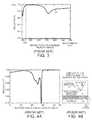
- FIG. 3is a diagram that shows the normal-incident reflectivity spectrum with the reflector design described in FIG. 2 .
- the stop-band of the spectrumcenters around 510 nm, and the short wavelength side of the stop-band is aligned to 450 nm.
- the reflectivity spectrumblue-shifts toward the short wavelength when the light incident angle increases from surface normal toward grazing angle to the reflector.
- the reflectorwas optimized to ensure high reflectivity for the light with wavelength of 450 nm over a broad range of incident angles.
- FIG. 4Ais a diagram that charts the reflectivity of the reflector structure 6 versus the angle of incidence of light with a wavelength of 450 nm reaching a point 11 on the reflector.
- the light with incident angles between 0 and 58 degreeare reflected by the DBR and the metal reflector, while the light with incident angle greater than 58 degree is reflected by the TIR layer.
- a normalized angular reflectanceis defined. Referring to FIG. 4B , light is assumed to be transmitted toward point 11 on the reflector from all directions with a uniform angular distribution. The amount of light incident on the point that is reaching the point 11 with an incident angle ⁇ is considered. Many different light rays may actually reach the point from this incident angle, where the light rays can be thought of as passing to the point in a cone shape.
- 4Brepresents a circle of origination points for such rays for the incident angle ⁇ . Accordingly, there is more light incident on point 11 for an incident angle of one degree than for an incident angle of zero degrees. This larger amount of light at larger angles is considered, and the corresponding total amount of reflected light is determined for angles zero (orthogonal) through 90 degrees (a grazing angle).
- the normalized angular reflectanceis then calculated by integrating the angular reflectivity ( FIG. 4A ) with a sine dependence of incident angle and normalized to a perfect angular reflectivity spectrum. This analysis is performed for light of a given wavelength, for example 450 nm, to compare the performance of the reflector for blue light emitted by the LED in the white LED assembly FIG. 1 .
- the prior art reflector structure of the LED device of FIG. 1has a reflectivity of approximately 97 percent for incident blue light (having a wavelength of 450 nm). Accordingly, most all of the blue light 4 traveling downward is then reflected back up the reflector so that it can escape the LED device.
- the reflector structure involving DBR 9is more effective than a simple mirror layer of a reflective metal such as silver.
- a blue LED devicehas an active layer involving indium, gallium and nitrogen.
- the active layeris configured to emit blue light that is quasi-monochromatic and non-coherent.
- the blue LEDalso has a transparent substrate (substantially transparent to visible light) and a reflector structure disposed on the backside of the substrate.
- the reflector structureincludes a Distributed Bragg Reflector (DBR) structure having layers configured to reflect green, yellow and red light as well as blue light.
- the DBR structureincludes a first portion where the thicknesses of the layers are relatively larger, and also includes a second portion where the thicknesses of the layers are relatively smaller.
- DBRDistributed Bragg Reflector
- the overall reflector structureIn addition to having a normalized angular reflectance of more than 97.5 percent for light of a wavelength in a first range between 440 nm-470 nm, the overall reflector structure also has a normalized angular reflectance of more than 95 percent for light of a wavelength in a second range between 500 nm-700 nm.
- the reflector structurereflects light passing from the transparent substrate and to the reflector structure such that the overall LED device has a Photon Recycling Efficiency (PRE) of more than 85 percent for light having a wavelength ranging from 500 nm to 700 nm.
- PREPhoton Recycling Efficiency
- FIG. 1(prior art) is a simplified cross-sectional diagram of a conventional so-called white LED.
- FIG. 2(prior art) is a table that sets forth the thicknesses and constituent materials of the various layer of the Distributed Bragg Reflector of the prior art LED device of FIG. 1 .
- FIG. 3(prior art) is a diagram that charts reflectivity versus the wavelength of incident light at a normal incident angle for the reflector structure of the prior art LED device of FIG. 1 .
- FIG. 4A(prior art) is a diagram that charts the reflectivity of the reflector structure of the prior art LED device of FIG. 1 versus the angle of incidence of light of a wavelength of 450 nm reaching a point on the reflector.
- FIG. 4B(prior art) is a conceptual diagram that illustrates a consideration involved in determining the normalized angular reflectance.
- FIG. 5is a diagram of a white LED assembly in accordance with one novel aspect.
- FIG. 6is a simplified cross-sectional diagram of a blue LED device within the white LED assembly of FIG. 5 .
- FIG. 7is a table that sets forth the thicknesses and constituent materials of the various layers of the novel reflector structure of FIGS. 5-6 .
- FIG. 8is a diagram that charts reflectivity versus wavelength of incident light normal to the reflector surface for the novel reflector structure of FIGS. 5-7 .
- FIG. 9is a table that compares the normalized angular reflectance at 450 nm and at 580 nm of the novel reflector structure of FIGS. 5-7 to the prior art reflector structure of FIGS. 1-4 .
- FIG. 10is a table that compares measured PRE values of the novel reflector structure of FIGS. 5-7 (at 450 nm, 580 nm, and 630 nm) with calculated PRE values to the prior art reflector structure of FIGS. 1-4 (at 450 nm, 580 nm, and 630 nm).
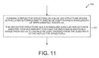
- FIG. 11is a flowchart of a method for forming a reflector structure on a blue LED that exhibits a high normalized angular reflectance for light having a wavelength in a range from 500 nm to 700 nm and in another range from 440 nm to 470 nm.
- FIG. 5is a simplified cross-sectional diagram of a white LED assembly 20 in accordance with one novel aspect.
- White LED assembly 20includes a blue LED device 21 , an aluminum core PCB 22 , a pair of wire bonds 23 and 24 , and an amount of phosphor 25 . Particles of phosphor are suspended in a dome structure of silicone as illustrated.
- LED device 21includes an epitaxial layer portion that includes, among other parts not illustrated, a p-type layer 26 , an active layer 27 , an n-type layer 28 , a buffer layer 29 , and two metal electrodes 30 and 31 .
- the layers 26 - 28are made of gallium nitride materials and the active layer includes indium such that the active layer emits so-called blue light as is known in the GaN blue LED art.
- the lightis quasi-monochromatic and non-coherent.
- the wavelength of the light emitted by the active layer 27has a relatively narrow bandwidth and is centered at approximately 450 nm.
- Transparent substrate 32is made of a transparent material, such as sapphire, SiC, GaN or AlN.
- the transparent substrate 32is a sapphire substrate.
- Reflector structure 34includes a total internal reflection (TIR) layer 35 , a multi-layer Distributed Bragg Reflector (DBR) structure 36 , and a reflective metal layer 37 .
- TIRtotal internal reflection
- DBRDistributed Bragg Reflector
- TIR layer 35 and the low refractive index layers of DBR 36can be made of low index dielectric material, such as SiO2, MgF2 or CaF2, and the high index layers of DBR 36 can be made of high index dielectric material, such TiO2, ZnSe, Si3N4, Nb2O5 or Ta2O5.
- Reflective metal layer 37can be made of any reflective metal, such as aluminum, silver, rhodium, platinum or nickel.
- Reflector structure 34is disposed on the “backside” of the substrate on the opposite side of the substrate from the epitaxial layers.
- FIG. 6is a more detailed cross-sectional diagram of the blue LED device 21 of the white LED assembly 20 of FIG. 5 .
- This lightAs is conventionally recognized, half of the light emitted from the active layer of an LED travels downward. This light, which in the present example has a wavelength of approximately 450 nm, should be reflected back upward by the reflector structure as described above in the background section. This light is represented in FIG. 5 by rays 38 and 39 .
- the novel reflector structure 34is not optimized for reflecting only blue light, and is not optimized for reflecting only yellow light, but rather the layers of the novel reflector structure are configured to reflect both blue and yellow light with high reflectivity.
- the novel reflector structure 34has a DBR that is substantially optimized for reflecting both blue light of approximately 450 nm and yellow light of approximately 580 nm.
- the reflector structure 34has a normalized angular reflectance of more than 95.5 percent for first light having a wavelength in a range from 500 nm to 700 nm (referred to here as yellow light), and also has a normalized angular reflectance of more than 97.5 percent second light having a wavelength in a range from 440 nm to 470 nm (referred to here as blue light).
- the photon efficacy (lumens per watt) of the overall novel LED assembly 20 of FIG. 5is improved as compared to the photon efficacy of the overall conventional LED assembly 1 of FIG. 1 largely due to the improved reflectivity of the reflector structure 34 in reflecting the light in the 500 nm to 700 nm range.
- Designing the DBR structure 34is not as simple as designing a first DBR optimized for reflecting yellow light, and designing a second DBR optimized for reflecting blue light, and then combining the two DBRs into a single composite DBR structure.
- Light passing through the DBR structure from one portion to the nextis affected in complex ways that complicates the determination of the thicknesses of the various layers, and the DBR is not entirely optimized for either yellow or blue light, but in a simplistic explanation a first portion 43 of the DBR 34 functions primarily to reflect yellow light, whereas a second portion 44 of the DBR 34 functions primarily to reflect blue light.
- the thicknesses of the layers of the first portion 43are larger, whereas the thicknesses of the layers of the second portion 44 are smaller.
- FIG. 7is a table that sets forth the thicknesses and compositions of the various layers of the reflector structure 34 in one specific embodiment.
- Row 45corresponds to the TIR layer 35 .
- Rows 46correspond to the first portion 43 of the DBR structure 36
- rows 47correspond to the second portion 44 of the DBR structure 36 .
- Row 48corresponds to the layer 37 of reflective metal.
- the values in the tableare for a design wavelength of 480 nm. Accordingly, the quarter-wave optical thickness (QWOT) values close to one in rows 47 indicate that the second portion 44 of the DBR structure will reflect blue light well.
- QWOTquarter-wave optical thickness
- FIG. 8is a chart of the reflectivity 49 versus wavelength for a normal incident angle for the overall reflector structure 34 .
- the chartcompares the reflectivity spectrum of the prior art reflector to that of the novel reflector.
- There are two distinct stop-band features for the novel reflectorindicating the complexity of the reflector design.
- Dashed curve 50is the reflectivity versus wavelength curve 50 of FIG. 3 that is reproduced in FIG. 8 for comparison purposes.
- FIG. 9is a table that sets forth the comparison.
- first light having a wavelength of 580 nmgenerally referred to herein as yellow light
- the novel reflector structure 34 of FIGS. 5-7has a reflectivity greater than 95.0 percent.
- second light having a wavelength of 450 nmgenerally referred to herein as blue light
- the novel reflector structure 34 of FIGS. 5-7has a reflectivity greater than 97.5 percent.
- the phosphorsabsorb the blue light emitted from the LED device 21 and down-convert it to longer wavelength (500 nm-700 nm) light.
- the long wavelength light re-emitted isotropically from the phosphor particles and some portion of long wavelength lightwill inevitably return to the LED surface.
- the probability of the returned light to escape the LED device 21is referred as the Photon Recycling Efficiency (PRE).
- the un-absorbed blue light emitted from the LED devicemay also be back-scattered by the phosphors and return to the LED device.
- a comprehensive ray-tracing modelwas employed to estimate the PRE for various wavelengths light.
- the absorption of the Indium Tin Oxide (ITO), the metal electrode, GaN material loss, the scattering structure and the reflectorwere all included in the simulation.
- the simulationwas performed using 450 nm light, 580 nm light, and 630 nm light.
- the percentage of light reflected(or “PRE”) is set forth in the table of FIG. 10 .
- the relatively small differences in reflectivity between the novel reflector structure and the conventional reflector structure indicated in the table of FIG. 9are amplified in the real device due to light within the LED device often making multiple bounces within the device.
- Simulationindicates that switching from the conventional reflector structure 6 of FIG. 1 to the novel reflector structure 34 of FIG. 5 results in more than a 5.0 percent improvement in Photon Recycling Efficiency for both 580 nm light and 630 nm light.
- FIG. 11is a flowchart of a method 100 in accordance with one novel aspect.
- a reflector structureis formed (step 101 ) on the backside of a substrate of a blue LED device.
- the active layer of the blue LED deviceis configured to emit light having a wavelength of approximately 440-470 nm, whereas the reflector structure has a normalized angular reflectance greater than 95.0% for light having a wavelength in a range from 500 nm to 700 nm.
- the reflector structurealso has a normalized angular reflectance greater than 97.5% for light having a wavelength of 440-470 nm.
- the reflector structure formed in step 101is the reflector structure 34 of FIGS. 5 and 6 , where this reflector structure 34 has a TIR layer, a DBR structure, and an underlying layer of metal of the thicknesses and constituent materials set forth in FIG. 7 .
Landscapes
- Physics & Mathematics (AREA)
- Chemical & Material Sciences (AREA)
- Inorganic Chemistry (AREA)
- General Physics & Mathematics (AREA)
- Optics & Photonics (AREA)
- Led Devices (AREA)
- Led Device Packages (AREA)
- Optical Elements Other Than Lenses (AREA)
Abstract
Description
Claims (27)
Priority Applications (1)
| Application Number | Priority Date | Filing Date | Title |
|---|---|---|---|
| US14/055,596US8981410B1 (en) | 2011-09-01 | 2013-10-16 | Distributed bragg reflector for reflecting light of multiple wavelengths from an LED |
Applications Claiming Priority (3)
| Application Number | Priority Date | Filing Date | Title |
|---|---|---|---|
| US201161530385P | 2011-09-01 | 2011-09-01 | |
| US13/587,746US8624482B2 (en) | 2011-09-01 | 2012-08-16 | Distributed bragg reflector for reflecting light of multiple wavelengths from an LED |
| US14/055,596US8981410B1 (en) | 2011-09-01 | 2013-10-16 | Distributed bragg reflector for reflecting light of multiple wavelengths from an LED |
Related Parent Applications (1)
| Application Number | Title | Priority Date | Filing Date |
|---|---|---|---|
| US13/587,746ContinuationUS8624482B2 (en) | 2011-09-01 | 2012-08-16 | Distributed bragg reflector for reflecting light of multiple wavelengths from an LED |
Publications (2)
| Publication Number | Publication Date |
|---|---|
| US20150069434A1 US20150069434A1 (en) | 2015-03-12 |
| US8981410B1true US8981410B1 (en) | 2015-03-17 |
Family
ID=47753072
Family Applications (2)
| Application Number | Title | Priority Date | Filing Date |
|---|---|---|---|
| US13/587,746Expired - Fee RelatedUS8624482B2 (en) | 2011-09-01 | 2012-08-16 | Distributed bragg reflector for reflecting light of multiple wavelengths from an LED |
| US14/055,596ActiveUS8981410B1 (en) | 2011-09-01 | 2013-10-16 | Distributed bragg reflector for reflecting light of multiple wavelengths from an LED |
Family Applications Before (1)
| Application Number | Title | Priority Date | Filing Date |
|---|---|---|---|
| US13/587,746Expired - Fee RelatedUS8624482B2 (en) | 2011-09-01 | 2012-08-16 | Distributed bragg reflector for reflecting light of multiple wavelengths from an LED |
Country Status (6)
| Country | Link |
|---|---|
| US (2) | US8624482B2 (en) |
| JP (2) | JP2014524674A (en) |
| KR (1) | KR20140012177A (en) |
| CN (1) | CN103650172A (en) |
| TW (1) | TWI462333B (en) |
| WO (1) | WO2013033152A1 (en) |
Families Citing this family (49)
| Publication number | Priority date | Publication date | Assignee | Title |
|---|---|---|---|---|
| US8624482B2 (en)* | 2011-09-01 | 2014-01-07 | Toshiba Techno Center Inc. | Distributed bragg reflector for reflecting light of multiple wavelengths from an LED |
| JP5731996B2 (en)* | 2012-02-21 | 2015-06-10 | 富士フイルム株式会社 | Semiconductor light emitting device |
| US9450152B2 (en) | 2012-05-29 | 2016-09-20 | Micron Technology, Inc. | Solid state transducer dies having reflective features over contacts and associated systems and methods |
| TWI590488B (en)* | 2013-01-25 | 2017-07-01 | 晶元光電股份有限公司 | Light-emitting element with high-efficiency reflective structure |
| JP2015028984A (en)* | 2013-07-30 | 2015-02-12 | 日亜化学工業株式会社 | Semiconductor light emitting element |
| JP2015050124A (en)* | 2013-09-03 | 2015-03-16 | スタンレー電気株式会社 | Light emitting device |
| US9865783B2 (en)* | 2013-09-09 | 2018-01-09 | Luminus, Inc. | Distributed Bragg reflector on an aluminum package for an LED |
| TWI637198B (en)* | 2013-09-30 | 2018-10-01 | 美商3M新設資產公司 | Polymeric multilayer optical film |
| TWI707484B (en) | 2013-11-14 | 2020-10-11 | 晶元光電股份有限公司 | Light-emitting device |
| KR20150062352A (en)* | 2013-11-29 | 2015-06-08 | 일진엘이디(주) | Light emitting diode having dielectric layer |
| US9419185B2 (en) | 2014-01-27 | 2016-08-16 | Glo Ab | Method of singulating LED wafer substrates into dice with LED device with Bragg reflector |
| KR102203461B1 (en) | 2014-07-10 | 2021-01-18 | 삼성전자주식회사 | Nano-sturucture semiconductor light emitting device |
| WO2016015746A1 (en)* | 2014-07-28 | 2016-02-04 | Osram Opto Semiconductors Gmbh | Dbr mirror and optoelectronic component having a dbr mirror |
| KR20160024170A (en) | 2014-08-25 | 2016-03-04 | 삼성전자주식회사 | Semiconductor light emitting device |
| US9606068B2 (en)* | 2014-08-27 | 2017-03-28 | Pacific Biosciences Of California, Inc. | Arrays of integrated analytical devices |
| KR20160034534A (en) | 2014-09-19 | 2016-03-30 | 삼성전자주식회사 | Semiconductor light emitting device |
| TWI705586B (en)* | 2014-09-26 | 2020-09-21 | 晶元光電股份有限公司 | Light-emitting device |
| DE102014115740A1 (en)* | 2014-10-29 | 2016-05-04 | Osram Opto Semiconductors Gmbh | Optoelectronic semiconductor chip |
| JP6394968B2 (en)* | 2015-02-06 | 2018-09-26 | 豊田合成株式会社 | Optical multilayer film and light emitting device |
| CN105098018B (en)* | 2015-06-01 | 2017-11-21 | 圆融光电科技股份有限公司 | The manufacture method of flip LED chips |
| KR102641239B1 (en)* | 2015-07-10 | 2024-02-29 | 서울바이오시스 주식회사 | Light emitting diode, method of fabricating the same, and light emitting device module having the same |
| CN105118849B (en)* | 2015-09-22 | 2018-07-31 | 上海和辉光电有限公司 | A kind of touch control organic light-emitting display panel |
| EP3357097B1 (en) | 2015-10-01 | 2020-12-16 | Cree, Inc. | Low optical loss flip chip solid state lighting device |
| JP6506899B2 (en)* | 2015-10-08 | 2019-04-24 | 日亜化学工業株式会社 | Light emitting device, integrated light emitting device and light emitting module |
| WO2017061127A1 (en) | 2015-10-08 | 2017-04-13 | Nichia Corporation | Light-emitting device, integrated light-emitting device, and light-emitting module |
| KR102471102B1 (en) | 2015-10-23 | 2022-11-25 | 서울바이오시스 주식회사 | Light emitting diode chip having distributed bragg reflector |
| KR102351775B1 (en)* | 2015-11-18 | 2022-01-14 | 휴렛-팩커드 디벨롭먼트 컴퍼니, 엘.피. | Image forming apparatus and light emitting device therein |
| JP6806446B2 (en)* | 2016-01-25 | 2021-01-06 | 日亜化学工業株式会社 | Semiconductor devices and their manufacturing methods |
| JP6683003B2 (en)* | 2016-05-11 | 2020-04-15 | 日亜化学工業株式会社 | Semiconductor element, semiconductor device, and method for manufacturing semiconductor element |
| JP6720747B2 (en) | 2016-07-19 | 2020-07-08 | 日亜化学工業株式会社 | Semiconductor device, base and manufacturing method thereof |
| JP6174776B1 (en)* | 2016-12-12 | 2017-08-02 | 中外炉工業株式会社 | Coating liquid supply device |
| WO2018180724A1 (en)* | 2017-03-28 | 2018-10-04 | 東芝マテリアル株式会社 | Semiconductor light emitting element |
| CN107492586B (en)* | 2017-08-01 | 2019-10-25 | 天津三安光电有限公司 | led |
| KR20190022326A (en)* | 2017-08-24 | 2019-03-06 | 서울바이오시스 주식회사 | Light emitting diode having distributed bragg reflector |
| US11031527B2 (en) | 2018-01-29 | 2021-06-08 | Creeled, Inc. | Reflective layers for light-emitting diodes |
| US11387389B2 (en) | 2018-01-29 | 2022-07-12 | Creeled, Inc. | Reflective layers for light-emitting diodes |
| US11923481B2 (en) | 2018-01-29 | 2024-03-05 | Creeled, Inc. | Reflective layers for light-emitting diodes |
| KR102496316B1 (en)* | 2018-05-30 | 2023-02-07 | 서울바이오시스 주식회사 | Light emitting diode chip having distributed bragg reflector |
| KR20200018996A (en)* | 2018-08-13 | 2020-02-21 | 서울바이오시스 주식회사 | Light emitting diode having light scattering pattern |
| US10879441B2 (en) | 2018-12-17 | 2020-12-29 | Cree, Inc. | Interconnects for light emitting diode chips |
| TWI842694B (en) | 2019-01-23 | 2024-05-21 | 晶元光電股份有限公司 | Light-emitting element with distributed bragg reflector |
| CN109817819B (en)* | 2019-01-31 | 2020-05-12 | 深圳市华星光电半导体显示技术有限公司 | White Organic Light Emitting Diode Devices with Enhanced Light Extraction |
| US10985294B2 (en) | 2019-03-19 | 2021-04-20 | Creeled, Inc. | Contact structures for light emitting diode chips |
| US11094848B2 (en) | 2019-08-16 | 2021-08-17 | Creeled, Inc. | Light-emitting diode chip structures |
| KR102861761B1 (en) | 2019-12-10 | 2025-09-18 | 삼성전자주식회사 | Light modulator, optical device including the light modulator and electrical apparatus including the optical device |
| KR102430331B1 (en)* | 2020-02-28 | 2022-08-05 | 가천대학교 산학협력단 | Si DISTRIBUTED BRAGG REFLECTOR AND FABRICATION METHOD THEREOF |
| WO2021251898A1 (en)* | 2020-06-10 | 2021-12-16 | Agency For Science, Technology And Research | Spatial light modulator and method of forming the same |
| US20240120452A1 (en)* | 2022-10-11 | 2024-04-11 | Creeled, Inc. | Reflectors for support structures in light-emitting diode packages |
| CN116014050B (en)* | 2022-12-30 | 2024-02-20 | 淮安澳洋顺昌光电技术有限公司 | a light-emitting element |
Citations (93)
| Publication number | Priority date | Publication date | Assignee | Title |
|---|---|---|---|---|
| JPH0363756A (en) | 1989-07-31 | 1991-03-19 | Fuji Xerox Co Ltd | Document editor |
| JPH0363757A (en) | 1989-07-31 | 1991-03-19 | Matsushita Electric Ind Co Ltd | Document preparing device |
| JPH03135041A (en) | 1989-10-20 | 1991-06-10 | Nippon Steel Corp | Manufacturing method of bonding thin wire for semiconductors |
| JPH03209096A (en) | 1989-11-17 | 1991-09-12 | Union Carbide Ind Gases Technol Corp | Cylinder having improved mixing characteristics |
| JPH03223832A (en) | 1990-01-30 | 1991-10-02 | Fuji Photo Optical Co Ltd | Self-photographing method for camera |
| JPH03250438A (en) | 1990-02-27 | 1991-11-08 | Sanyo Electric Co Ltd | Optical recording medium |
| JPH04118371A (en) | 1990-09-05 | 1992-04-20 | Koyo Seiko Co Ltd | Rack-and-pinion type steering gear |
| JPH04118370A (en) | 1990-09-07 | 1992-04-20 | Mazda Motor Corp | Hydraulic driver for rear-wheel steering system |
| US5306662A (en) | 1991-11-08 | 1994-04-26 | Nichia Chemical Industries, Ltd. | Method of manufacturing P-type compound semiconductor |
| US5408120A (en) | 1992-07-23 | 1995-04-18 | Toyoda Gosei Co., Ltd. | Light-emitting device of gallium nitride compound semiconductor |
| US5563422A (en) | 1993-04-28 | 1996-10-08 | Nichia Chemical Industries, Ltd. | Gallium nitride-based III-V group compound semiconductor device and method of producing the same |
| US5578839A (en) | 1992-11-20 | 1996-11-26 | Nichia Chemical Industries, Ltd. | Light-emitting gallium nitride-based compound semiconductor device |
| JP2626431B2 (en) | 1992-10-29 | 1997-07-02 | 豊田合成株式会社 | Nitrogen-3 group element compound semiconductor light emitting device |
| JP2666237B2 (en) | 1994-09-20 | 1997-10-22 | 豊田合成株式会社 | Group III nitride semiconductor light emitting device |
| JP2681733B2 (en) | 1992-10-29 | 1997-11-26 | 豊田合成株式会社 | Nitrogen-3 group element compound semiconductor light emitting device |
| JP2735057B2 (en) | 1994-12-22 | 1998-04-02 | 日亜化学工業株式会社 | Nitride semiconductor light emitting device |
| US5777350A (en) | 1994-12-02 | 1998-07-07 | Nichia Chemical Industries, Ltd. | Nitride semiconductor light-emitting device |
| JP2778405B2 (en) | 1993-03-12 | 1998-07-23 | 日亜化学工業株式会社 | Gallium nitride based compound semiconductor light emitting device |
| JP2785254B2 (en) | 1993-06-28 | 1998-08-13 | 日亜化学工業株式会社 | Gallium nitride based compound semiconductor light emitting device |
| JP2803741B2 (en) | 1993-03-19 | 1998-09-24 | 日亜化学工業株式会社 | Gallium nitride based compound semiconductor electrode forming method |
| JP2827794B2 (en) | 1993-02-05 | 1998-11-25 | 日亜化学工業株式会社 | Method for growing p-type gallium nitride |
| JP2890396B2 (en) | 1995-03-27 | 1999-05-10 | 日亜化学工業株式会社 | Nitride semiconductor light emitting device |
| JP2917742B2 (en) | 1992-07-07 | 1999-07-12 | 日亜化学工業株式会社 | Gallium nitride based compound semiconductor light emitting device and method of manufacturing the same |
| US5959401A (en) | 1996-05-21 | 1999-09-28 | Toyoda Gosei Co., Ltd. | Light-emitting semiconductor device using group III nitride compound |
| US5959307A (en) | 1995-11-06 | 1999-09-28 | Nichia Chemical Industries Ltd. | Nitride semiconductor device |
| JP2956489B2 (en) | 1994-06-24 | 1999-10-04 | 日亜化学工業株式会社 | Crystal growth method of gallium nitride based compound semiconductor |
| US6005258A (en) | 1994-03-22 | 1999-12-21 | Toyoda Gosei Co., Ltd. | Light-emitting semiconductor device using group III Nitrogen compound having emission layer doped with donor and acceptor impurities |
| US6040588A (en) | 1996-09-08 | 2000-03-21 | Toyoda Gosei Co., Ltd. | Semiconductor light-emitting device |
| JP3063756B1 (en) | 1998-10-06 | 2000-07-12 | 日亜化学工業株式会社 | Nitride semiconductor device |
| JP3063757B1 (en) | 1998-11-17 | 2000-07-12 | 日亜化学工業株式会社 | Nitride semiconductor device |
| JP3135041B2 (en) | 1995-09-29 | 2001-02-13 | 日亜化学工業株式会社 | Nitride semiconductor light emitting device |
| JP3223832B2 (en) | 1997-02-24 | 2001-10-29 | 日亜化学工業株式会社 | Nitride semiconductor device and semiconductor laser diode |
| JP3250438B2 (en) | 1995-03-29 | 2002-01-28 | 日亜化学工業株式会社 | Nitride semiconductor light emitting device |
| JP3314666B2 (en) | 1997-06-09 | 2002-08-12 | 日亜化学工業株式会社 | Nitride semiconductor device |
| JP3344257B2 (en) | 1997-01-17 | 2002-11-11 | 豊田合成株式会社 | Gallium nitride based compound semiconductor and device manufacturing method |
| JP3374737B2 (en) | 1997-01-09 | 2003-02-10 | 日亜化学工業株式会社 | Nitride semiconductor device |
| JP3424629B2 (en) | 1998-12-08 | 2003-07-07 | 日亜化学工業株式会社 | Nitride semiconductor device |
| JP3427265B2 (en) | 1998-12-08 | 2003-07-14 | 日亜化学工業株式会社 | Nitride semiconductor device |
| US6657236B1 (en) | 1999-12-03 | 2003-12-02 | Cree Lighting Company | Enhanced light extraction in LEDs through the use of internal and external optical elements |
| JP3506874B2 (en) | 1997-03-24 | 2004-03-15 | 豊田合成株式会社 | Nitrogen-3 group element compound semiconductor light emitting device |
| JP3511970B2 (en) | 1995-06-15 | 2004-03-29 | 日亜化学工業株式会社 | Nitride semiconductor light emitting device |
| JP3548442B2 (en) | 1994-09-22 | 2004-07-28 | 日亜化学工業株式会社 | Gallium nitride based compound semiconductor light emitting device |
| JP3551101B2 (en) | 1999-03-29 | 2004-08-04 | 日亜化学工業株式会社 | Nitride semiconductor device |
| US6800500B2 (en) | 1999-02-05 | 2004-10-05 | Lumileds Lighting U.S., Llc | III-nitride light emitting devices fabricated by substrate removal |
| US6838693B2 (en) | 2000-07-07 | 2005-01-04 | Nichia Corporation | Nitride semiconductor device |
| US6849881B1 (en) | 1999-11-19 | 2005-02-01 | Osram Gmbh | Optical semiconductor device comprising a multiple quantum well structure |
| JP3622562B2 (en) | 1998-03-12 | 2005-02-23 | 日亜化学工業株式会社 | Nitride semiconductor light emitting diode |
| US6891197B2 (en) | 2001-05-09 | 2005-05-10 | Lumileds Lighting U.S., Llc | Semiconductor LED flip-chip with dielectric coating on the mesa |
| JP3646649B2 (en) | 1994-09-22 | 2005-05-11 | 日亜化学工業株式会社 | Gallium nitride compound semiconductor light emitting device |
| JP3654738B2 (en) | 1997-04-07 | 2005-06-02 | 豊田合成株式会社 | Group 3 nitride semiconductor light emitting device |
| US6906352B2 (en) | 2001-01-16 | 2005-06-14 | Cree, Inc. | Group III nitride LED with undoped cladding layer and multiple quantum well |
| WO2005055382A1 (en) | 2003-12-01 | 2005-06-16 | Nl-Nanosemiconductor Gmbh | Tilted cavity semiconductor optoelectronic device and method of making same |
| US6916676B2 (en) | 2002-01-28 | 2005-07-12 | Nichia Corporation | Method for producing a nitride semiconductor element |
| US6951695B2 (en) | 2001-06-08 | 2005-10-04 | Cree, Inc. | High surface quality GaN wafer and method of fabricating same |
| US6977395B2 (en) | 2001-07-12 | 2005-12-20 | Nichia Corporation | Semiconductor device |
| US7026653B2 (en) | 2004-01-27 | 2006-04-11 | Lumileds Lighting, U.S., Llc | Semiconductor light emitting devices including current spreading layers |
| JP3780887B2 (en) | 1996-09-08 | 2006-05-31 | 豊田合成株式会社 | Semiconductor light emitting device and manufacturing method thereof |
| JP3786114B2 (en) | 2000-11-21 | 2006-06-14 | 日亜化学工業株式会社 | Nitride semiconductor device |
| JP3795624B2 (en) | 1997-03-31 | 2006-07-12 | 豊田合成株式会社 | Nitrogen-3 group element compound semiconductor light emitting device |
| US7115908B2 (en) | 2004-01-30 | 2006-10-03 | Philips Lumileds Lighting Company, Llc | III-nitride light emitting device with reduced polarization fields |
| JP3890930B2 (en) | 1995-03-29 | 2007-03-07 | 日亜化学工業株式会社 | Nitride semiconductor light emitting device |
| US7193246B1 (en) | 1998-03-12 | 2007-03-20 | Nichia Corporation | Nitride semiconductor device |
| US20070145380A1 (en) | 2006-05-19 | 2007-06-28 | Shum Frank T | Low optical loss electrode structures for LEDs |
| US7262436B2 (en) | 1997-12-15 | 2007-08-28 | Philips Lumileds Lighting Company, Llc | III-nitride semiconductor light emitting device having a silver p-contact |
| US7312474B2 (en) | 2001-05-30 | 2007-12-25 | Cree, Inc. | Group III nitride based superlattice structures |
| US7335920B2 (en) | 2005-01-24 | 2008-02-26 | Cree, Inc. | LED with current confinement structure and surface roughening |
| US7345297B2 (en) | 2004-02-09 | 2008-03-18 | Nichia Corporation | Nitride semiconductor device |
| US7348602B2 (en) | 1999-03-29 | 2008-03-25 | Nichia Corporation | Nitride semiconductor device |
| JP4118371B2 (en) | 1997-12-15 | 2008-07-16 | フィリップス ルミレッズ ライティング カンパニー リミテッド ライアビリティ カンパニー | Nitride semiconductor light emitting device having silver as electrode, method for manufacturing the same, and semiconductor optoelectronic device |
| JP4118370B2 (en) | 1997-12-15 | 2008-07-16 | フィリップス ルミレッズ ライティング カンパニー リミテッド ライアビリティ カンパニー | Nitride semiconductor light-emitting device having reflective p-electrode, method for manufacturing the same, and semiconductor optoelectronic device |
| US7442966B2 (en) | 2002-09-30 | 2008-10-28 | Osram Gmbh | Electromagnetic radiation emitting semiconductor chip and procedure for its production |
| US7446345B2 (en) | 2005-04-29 | 2008-11-04 | Cree, Inc. | Light emitting devices with active layers that extend into opened pits |
| US7547908B2 (en) | 2006-12-22 | 2009-06-16 | Philips Lumilieds Lighting Co, Llc | III-nitride light emitting devices grown on templates to reduce strain |
| US7709851B2 (en) | 2004-04-14 | 2010-05-04 | Osram Opto Semiconductors Gmbh | Light-emitting diode chip including a mirror layer and a light-generating active zone |
| US20100123948A1 (en) | 2007-02-28 | 2010-05-20 | Maxim Integrated Products, Inc. | Bragg Mirror and Method for Making Same |
| US7737459B2 (en) | 2004-09-22 | 2010-06-15 | Cree, Inc. | High output group III nitride light emitting diodes |
| US7754514B2 (en) | 2006-08-22 | 2010-07-13 | Toyoda Gosei Co., Ltd. | Method of making a light emitting element |
| US7791101B2 (en) | 2008-03-28 | 2010-09-07 | Cree, Inc. | Indium gallium nitride-based ohmic contact layers for gallium nitride-based devices |
| US7791061B2 (en) | 2004-05-18 | 2010-09-07 | Cree, Inc. | External extraction light emitting diode based upon crystallographic faceted surfaces |
| US7795623B2 (en) | 2004-06-30 | 2010-09-14 | Cree, Inc. | Light emitting devices having current reducing structures and methods of forming light emitting devices having current reducing structures |
| KR100993112B1 (en) | 2008-05-08 | 2010-11-08 | 엘지이노텍 주식회사 | Light emitting device |
| JP4629178B2 (en) | 1998-10-06 | 2011-02-09 | 日亜化学工業株式会社 | Nitride semiconductor device |
| KR20110027341A (en) | 2009-09-10 | 2011-03-16 | 주식회사 에피밸리 | Semiconductor light emitting device |
| US7910945B2 (en) | 2006-06-30 | 2011-03-22 | Cree, Inc. | Nickel tin bonding system with barrier layer for semiconductor wafers and devices |
| US7939844B2 (en) | 2000-05-26 | 2011-05-10 | Osram Gmbh | Light-emitting-diode chip comprising a sequence of GAN-based epitaxial layers which emit radiation and a method for producing the same |
| US20110114969A1 (en) | 2009-11-13 | 2011-05-19 | Seoul Opto Device Co., Ltd. | Light emitting diode chip having distributed bragg reflector, method of fabricating the same, and light emitting diode package having distributed bragg reflector |
| WO2011099771A2 (en) | 2010-02-12 | 2011-08-18 | Seoul Opto Device Co., Ltd. | Light emitting diode chip having distributed bragg reflector and method of fabricating the same |
| US8021904B2 (en) | 2007-02-01 | 2011-09-20 | Cree, Inc. | Ohmic contacts to nitrogen polarity GaN |
| US8030665B2 (en) | 2002-07-08 | 2011-10-04 | Nichia Corporation | Nitride semiconductor device comprising bonded substrate and fabrication method of the same |
| JP4904261B2 (en) | 2004-06-30 | 2012-03-28 | クリー インコーポレイテッド | Light emitting device having current blocking structure and method for manufacturing light emitting device having current blocking structure |
| US20120286309A1 (en)* | 2011-05-13 | 2012-11-15 | Samsung Led Co., Ltd. | Semiconductor light emitting diode chip and light emitting device using the same |
| US20130032845A1 (en)* | 2011-08-02 | 2013-02-07 | Bridgelux, Inc. | High temperature gold-free wafer bonding for light emitting diodes |
| US8624482B2 (en)* | 2011-09-01 | 2014-01-07 | Toshiba Techno Center Inc. | Distributed bragg reflector for reflecting light of multiple wavelengths from an LED |
Family Cites Families (2)
| Publication number | Priority date | Publication date | Assignee | Title |
|---|---|---|---|---|
| JPH0217701U (en)* | 1988-07-19 | 1990-02-06 | ||
| DE102004045947A1 (en)* | 2004-06-30 | 2006-01-19 | Osram Opto Semiconductors Gmbh | LED array |
- 2012
- 2012-08-16USUS13/587,746patent/US8624482B2/ennot_activeExpired - Fee Related
- 2012-08-29KRKR1020137033695Apatent/KR20140012177A/ennot_activeCeased
- 2012-08-29CNCN201280028532.5Apatent/CN103650172A/enactivePending
- 2012-08-29JPJP2014527362Apatent/JP2014524674A/enactivePending
- 2012-08-29WOPCT/US2012/052782patent/WO2013033152A1/enactiveApplication Filing
- 2012-08-30TWTW101131502Apatent/TWI462333B/ennot_activeIP Right Cessation
- 2013
- 2013-10-16USUS14/055,596patent/US8981410B1/enactiveActive
- 2015
- 2015-07-07JPJP2015136335Apatent/JP2016001740A/enactivePending
Patent Citations (116)
| Publication number | Priority date | Publication date | Assignee | Title |
|---|---|---|---|---|
| JPH0363756A (en) | 1989-07-31 | 1991-03-19 | Fuji Xerox Co Ltd | Document editor |
| JPH0363757A (en) | 1989-07-31 | 1991-03-19 | Matsushita Electric Ind Co Ltd | Document preparing device |
| JPH03135041A (en) | 1989-10-20 | 1991-06-10 | Nippon Steel Corp | Manufacturing method of bonding thin wire for semiconductors |
| JPH03209096A (en) | 1989-11-17 | 1991-09-12 | Union Carbide Ind Gases Technol Corp | Cylinder having improved mixing characteristics |
| JPH03223832A (en) | 1990-01-30 | 1991-10-02 | Fuji Photo Optical Co Ltd | Self-photographing method for camera |
| JPH03250438A (en) | 1990-02-27 | 1991-11-08 | Sanyo Electric Co Ltd | Optical recording medium |
| JPH04118371A (en) | 1990-09-05 | 1992-04-20 | Koyo Seiko Co Ltd | Rack-and-pinion type steering gear |
| JPH04118370A (en) | 1990-09-07 | 1992-04-20 | Mazda Motor Corp | Hydraulic driver for rear-wheel steering system |
| US5468678A (en) | 1991-11-08 | 1995-11-21 | Nichia Chemical Industries, Ltd. | Method of manufacturing P-type compound semiconductor |
| US5306662A (en) | 1991-11-08 | 1994-04-26 | Nichia Chemical Industries, Ltd. | Method of manufacturing P-type compound semiconductor |
| JP2917742B2 (en) | 1992-07-07 | 1999-07-12 | 日亜化学工業株式会社 | Gallium nitride based compound semiconductor light emitting device and method of manufacturing the same |
| US5408120A (en) | 1992-07-23 | 1995-04-18 | Toyoda Gosei Co., Ltd. | Light-emitting device of gallium nitride compound semiconductor |
| USRE36747E (en) | 1992-07-23 | 2000-06-27 | Toyoda Gosei Co., Ltd | Light-emitting device of gallium nitride compound semiconductor |
| JP2681733B2 (en) | 1992-10-29 | 1997-11-26 | 豊田合成株式会社 | Nitrogen-3 group element compound semiconductor light emitting device |
| JP2626431B2 (en) | 1992-10-29 | 1997-07-02 | 豊田合成株式会社 | Nitrogen-3 group element compound semiconductor light emitting device |
| US5747832A (en) | 1992-11-20 | 1998-05-05 | Nichia Chemical Industries, Ltd. | Light-emitting gallium nitride-based compound semiconductor device |
| US5578839A (en) | 1992-11-20 | 1996-11-26 | Nichia Chemical Industries, Ltd. | Light-emitting gallium nitride-based compound semiconductor device |
| US6215133B1 (en) | 1992-11-20 | 2001-04-10 | Nichia Chemical Industries, Ltd. | Light-emitting gallium nitride-based compound semiconductor device |
| US5734182A (en) | 1992-11-20 | 1998-03-31 | Nichia Chemical Industries Ltd. | Light-emitting gallium nitride-based compound semiconducor device |
| JP2827794B2 (en) | 1993-02-05 | 1998-11-25 | 日亜化学工業株式会社 | Method for growing p-type gallium nitride |
| JP2778405B2 (en) | 1993-03-12 | 1998-07-23 | 日亜化学工業株式会社 | Gallium nitride based compound semiconductor light emitting device |
| JP2803741B2 (en) | 1993-03-19 | 1998-09-24 | 日亜化学工業株式会社 | Gallium nitride based compound semiconductor electrode forming method |
| US6610995B2 (en) | 1993-04-28 | 2003-08-26 | Nichia Corporation | Gallium nitride-based III-V group compound semiconductor |
| US5563422A (en) | 1993-04-28 | 1996-10-08 | Nichia Chemical Industries, Ltd. | Gallium nitride-based III-V group compound semiconductor device and method of producing the same |
| JP2785254B2 (en) | 1993-06-28 | 1998-08-13 | 日亜化学工業株式会社 | Gallium nitride based compound semiconductor light emitting device |
| US6265726B1 (en) | 1994-03-22 | 2001-07-24 | Toyoda Gosei Co., Ltd. | Light-emitting aluminum gallium indium nitride compound semiconductor device having an improved luminous intensity |
| US7138286B2 (en) | 1994-03-22 | 2006-11-21 | Toyoda Gosei Co., Ltd. | Light-emitting semiconductor device using group III nitrogen compound |
| US6005258A (en) | 1994-03-22 | 1999-12-21 | Toyoda Gosei Co., Ltd. | Light-emitting semiconductor device using group III Nitrogen compound having emission layer doped with donor and acceptor impurities |
| JP2956489B2 (en) | 1994-06-24 | 1999-10-04 | 日亜化学工業株式会社 | Crystal growth method of gallium nitride based compound semiconductor |
| US5753939A (en) | 1994-09-20 | 1998-05-19 | Toyoda Gosei Kk | Light-emitting semiconductor device using a Group III nitride compound and having a contact layer upon which an electrode is formed |
| JP2666237B2 (en) | 1994-09-20 | 1997-10-22 | 豊田合成株式会社 | Group III nitride semiconductor light emitting device |
| JP3548442B2 (en) | 1994-09-22 | 2004-07-28 | 日亜化学工業株式会社 | Gallium nitride based compound semiconductor light emitting device |
| JP3646649B2 (en) | 1994-09-22 | 2005-05-11 | 日亜化学工業株式会社 | Gallium nitride compound semiconductor light emitting device |
| US5777350A (en) | 1994-12-02 | 1998-07-07 | Nichia Chemical Industries, Ltd. | Nitride semiconductor light-emitting device |
| JP2735057B2 (en) | 1994-12-22 | 1998-04-02 | 日亜化学工業株式会社 | Nitride semiconductor light emitting device |
| JP2890396B2 (en) | 1995-03-27 | 1999-05-10 | 日亜化学工業株式会社 | Nitride semiconductor light emitting device |
| JP3890930B2 (en) | 1995-03-29 | 2007-03-07 | 日亜化学工業株式会社 | Nitride semiconductor light emitting device |
| JP3250438B2 (en) | 1995-03-29 | 2002-01-28 | 日亜化学工業株式会社 | Nitride semiconductor light emitting device |
| JP3511970B2 (en) | 1995-06-15 | 2004-03-29 | 日亜化学工業株式会社 | Nitride semiconductor light emitting device |
| JP3135041B2 (en) | 1995-09-29 | 2001-02-13 | 日亜化学工業株式会社 | Nitride semiconductor light emitting device |
| US5959307A (en) | 1995-11-06 | 1999-09-28 | Nichia Chemical Industries Ltd. | Nitride semiconductor device |
| US5959401A (en) | 1996-05-21 | 1999-09-28 | Toyoda Gosei Co., Ltd. | Light-emitting semiconductor device using group III nitride compound |
| JP3209096B2 (en) | 1996-05-21 | 2001-09-17 | 豊田合成株式会社 | Group III nitride compound semiconductor light emitting device |
| US6326236B1 (en) | 1996-09-08 | 2001-12-04 | Toyoda Gosei Co., Ltd. | Semiconductor light-emitting device and manufacturing method thereof |
| US6420733B2 (en) | 1996-09-08 | 2002-07-16 | Toyoda Gosei Co., Ltd. | Semiconductor light-emitting device and manufacturing method thereof |
| US6541293B2 (en) | 1996-09-08 | 2003-04-01 | Toyoda Gosei Co., Ltd. | Semiconductor light-emitting device and manufacturing method thereof |
| US6040588A (en) | 1996-09-08 | 2000-03-21 | Toyoda Gosei Co., Ltd. | Semiconductor light-emitting device |
| JP3780887B2 (en) | 1996-09-08 | 2006-05-31 | 豊田合成株式会社 | Semiconductor light emitting device and manufacturing method thereof |
| JP3304787B2 (en) | 1996-09-08 | 2002-07-22 | 豊田合成株式会社 | Semiconductor light emitting device and method of manufacturing the same |
| JP3374737B2 (en) | 1997-01-09 | 2003-02-10 | 日亜化学工業株式会社 | Nitride semiconductor device |
| JP3344257B2 (en) | 1997-01-17 | 2002-11-11 | 豊田合成株式会社 | Gallium nitride based compound semiconductor and device manufacturing method |
| JP3223832B2 (en) | 1997-02-24 | 2001-10-29 | 日亜化学工業株式会社 | Nitride semiconductor device and semiconductor laser diode |
| JP3506874B2 (en) | 1997-03-24 | 2004-03-15 | 豊田合成株式会社 | Nitrogen-3 group element compound semiconductor light emitting device |
| JP3795624B2 (en) | 1997-03-31 | 2006-07-12 | 豊田合成株式会社 | Nitrogen-3 group element compound semiconductor light emitting device |
| JP3654738B2 (en) | 1997-04-07 | 2005-06-02 | 豊田合成株式会社 | Group 3 nitride semiconductor light emitting device |
| JP3314666B2 (en) | 1997-06-09 | 2002-08-12 | 日亜化学工業株式会社 | Nitride semiconductor device |
| JP4118370B2 (en) | 1997-12-15 | 2008-07-16 | フィリップス ルミレッズ ライティング カンパニー リミテッド ライアビリティ カンパニー | Nitride semiconductor light-emitting device having reflective p-electrode, method for manufacturing the same, and semiconductor optoelectronic device |
| US7262436B2 (en) | 1997-12-15 | 2007-08-28 | Philips Lumileds Lighting Company, Llc | III-nitride semiconductor light emitting device having a silver p-contact |
| JP4118371B2 (en) | 1997-12-15 | 2008-07-16 | フィリップス ルミレッズ ライティング カンパニー リミテッド ライアビリティ カンパニー | Nitride semiconductor light emitting device having silver as electrode, method for manufacturing the same, and semiconductor optoelectronic device |
| US7193246B1 (en) | 1998-03-12 | 2007-03-20 | Nichia Corporation | Nitride semiconductor device |
| US7947994B2 (en) | 1998-03-12 | 2011-05-24 | Nichia Corporation | Nitride semiconductor device |
| JP3622562B2 (en) | 1998-03-12 | 2005-02-23 | 日亜化学工業株式会社 | Nitride semiconductor light emitting diode |
| US7402838B2 (en) | 1998-03-12 | 2008-07-22 | Nichia Corporation | Nitride semiconductor device |
| JP4629178B2 (en) | 1998-10-06 | 2011-02-09 | 日亜化学工業株式会社 | Nitride semiconductor device |
| JP3063756B1 (en) | 1998-10-06 | 2000-07-12 | 日亜化学工業株式会社 | Nitride semiconductor device |
| JP3063757B1 (en) | 1998-11-17 | 2000-07-12 | 日亜化学工業株式会社 | Nitride semiconductor device |
| JP3427265B2 (en) | 1998-12-08 | 2003-07-14 | 日亜化学工業株式会社 | Nitride semiconductor device |
| JP3424629B2 (en) | 1998-12-08 | 2003-07-07 | 日亜化学工業株式会社 | Nitride semiconductor device |
| US7491565B2 (en) | 1999-02-05 | 2009-02-17 | Philips Lumileds Lighting Company, Llc | III-nitride light emitting devices fabricated by substrate removal |
| US6800500B2 (en) | 1999-02-05 | 2004-10-05 | Lumileds Lighting U.S., Llc | III-nitride light emitting devices fabricated by substrate removal |
| JP4860024B2 (en) | 1999-02-05 | 2012-01-25 | フィリップス ルミレッズ ライティング カンパニー リミテッド ライアビリティ カンパニー | InXAlYGaZN light emitting device and manufacturing method thereof |
| US7348602B2 (en) | 1999-03-29 | 2008-03-25 | Nichia Corporation | Nitride semiconductor device |
| JP3551101B2 (en) | 1999-03-29 | 2004-08-04 | 日亜化学工業株式会社 | Nitride semiconductor device |
| US6849881B1 (en) | 1999-11-19 | 2005-02-01 | Osram Gmbh | Optical semiconductor device comprising a multiple quantum well structure |
| US7106090B2 (en) | 1999-11-19 | 2006-09-12 | Osram Opto Semiconductors Gmbh | Optical semiconductor device with multiple quantum well structure |
| US6657236B1 (en) | 1999-12-03 | 2003-12-02 | Cree Lighting Company | Enhanced light extraction in LEDs through the use of internal and external optical elements |
| US7939844B2 (en) | 2000-05-26 | 2011-05-10 | Osram Gmbh | Light-emitting-diode chip comprising a sequence of GAN-based epitaxial layers which emit radiation and a method for producing the same |
| US6838693B2 (en) | 2000-07-07 | 2005-01-04 | Nichia Corporation | Nitride semiconductor device |
| JP3786114B2 (en) | 2000-11-21 | 2006-06-14 | 日亜化学工業株式会社 | Nitride semiconductor device |
| US6906352B2 (en) | 2001-01-16 | 2005-06-14 | Cree, Inc. | Group III nitride LED with undoped cladding layer and multiple quantum well |
| US6891197B2 (en) | 2001-05-09 | 2005-05-10 | Lumileds Lighting U.S., Llc | Semiconductor LED flip-chip with dielectric coating on the mesa |
| US7312474B2 (en) | 2001-05-30 | 2007-12-25 | Cree, Inc. | Group III nitride based superlattice structures |
| US6951695B2 (en) | 2001-06-08 | 2005-10-04 | Cree, Inc. | High surface quality GaN wafer and method of fabricating same |
| US6977395B2 (en) | 2001-07-12 | 2005-12-20 | Nichia Corporation | Semiconductor device |
| US6916676B2 (en) | 2002-01-28 | 2005-07-12 | Nichia Corporation | Method for producing a nitride semiconductor element |
| US8030665B2 (en) | 2002-07-08 | 2011-10-04 | Nichia Corporation | Nitride semiconductor device comprising bonded substrate and fabrication method of the same |
| US7442966B2 (en) | 2002-09-30 | 2008-10-28 | Osram Gmbh | Electromagnetic radiation emitting semiconductor chip and procedure for its production |
| WO2005055382A1 (en) | 2003-12-01 | 2005-06-16 | Nl-Nanosemiconductor Gmbh | Tilted cavity semiconductor optoelectronic device and method of making same |
| US7026653B2 (en) | 2004-01-27 | 2006-04-11 | Lumileds Lighting, U.S., Llc | Semiconductor light emitting devices including current spreading layers |
| US7115908B2 (en) | 2004-01-30 | 2006-10-03 | Philips Lumileds Lighting Company, Llc | III-nitride light emitting device with reduced polarization fields |
| US7345297B2 (en) | 2004-02-09 | 2008-03-18 | Nichia Corporation | Nitride semiconductor device |
| US7709851B2 (en) | 2004-04-14 | 2010-05-04 | Osram Opto Semiconductors Gmbh | Light-emitting diode chip including a mirror layer and a light-generating active zone |
| US7791061B2 (en) | 2004-05-18 | 2010-09-07 | Cree, Inc. | External extraction light emitting diode based upon crystallographic faceted surfaces |
| JP4904261B2 (en) | 2004-06-30 | 2012-03-28 | クリー インコーポレイテッド | Light emitting device having current blocking structure and method for manufacturing light emitting device having current blocking structure |
| US7795623B2 (en) | 2004-06-30 | 2010-09-14 | Cree, Inc. | Light emitting devices having current reducing structures and methods of forming light emitting devices having current reducing structures |
| US7737459B2 (en) | 2004-09-22 | 2010-06-15 | Cree, Inc. | High output group III nitride light emitting diodes |
| US7335920B2 (en) | 2005-01-24 | 2008-02-26 | Cree, Inc. | LED with current confinement structure and surface roughening |
| US7446345B2 (en) | 2005-04-29 | 2008-11-04 | Cree, Inc. | Light emitting devices with active layers that extend into opened pits |
| US7611917B2 (en) | 2005-04-29 | 2009-11-03 | Cree, Inc. | Methods of forming light emitting devices with active layers that extend into opened pits |
| US20070145380A1 (en) | 2006-05-19 | 2007-06-28 | Shum Frank T | Low optical loss electrode structures for LEDs |
| JP2009537982A (en) | 2006-05-19 | 2009-10-29 | ブリッジラックス インコーポレイテッド | Low optical loss electrode structure for LED |
| US7897992B2 (en) | 2006-05-19 | 2011-03-01 | Bridgelux, Inc. | Low optical loss electrode structures for LEDs |
| US7910945B2 (en) | 2006-06-30 | 2011-03-22 | Cree, Inc. | Nickel tin bonding system with barrier layer for semiconductor wafers and devices |
| US7754514B2 (en) | 2006-08-22 | 2010-07-13 | Toyoda Gosei Co., Ltd. | Method of making a light emitting element |
| US7547908B2 (en) | 2006-12-22 | 2009-06-16 | Philips Lumilieds Lighting Co, Llc | III-nitride light emitting devices grown on templates to reduce strain |
| US8021904B2 (en) | 2007-02-01 | 2011-09-20 | Cree, Inc. | Ohmic contacts to nitrogen polarity GaN |
| US20100123948A1 (en) | 2007-02-28 | 2010-05-20 | Maxim Integrated Products, Inc. | Bragg Mirror and Method for Making Same |
| US7791101B2 (en) | 2008-03-28 | 2010-09-07 | Cree, Inc. | Indium gallium nitride-based ohmic contact layers for gallium nitride-based devices |
| KR100993112B1 (en) | 2008-05-08 | 2010-11-08 | 엘지이노텍 주식회사 | Light emitting device |
| KR20110027341A (en) | 2009-09-10 | 2011-03-16 | 주식회사 에피밸리 | Semiconductor light emitting device |
| US20110114969A1 (en) | 2009-11-13 | 2011-05-19 | Seoul Opto Device Co., Ltd. | Light emitting diode chip having distributed bragg reflector, method of fabricating the same, and light emitting diode package having distributed bragg reflector |
| WO2011099771A2 (en) | 2010-02-12 | 2011-08-18 | Seoul Opto Device Co., Ltd. | Light emitting diode chip having distributed bragg reflector and method of fabricating the same |
| JP2011166146A (en) | 2010-02-12 | 2011-08-25 | Seoul Opto Devices Co Ltd | Light-emitting diode chip having distributed bragg reflector and method of fabricating the same |
| US20120286309A1 (en)* | 2011-05-13 | 2012-11-15 | Samsung Led Co., Ltd. | Semiconductor light emitting diode chip and light emitting device using the same |
| US20130032845A1 (en)* | 2011-08-02 | 2013-02-07 | Bridgelux, Inc. | High temperature gold-free wafer bonding for light emitting diodes |
| US8624482B2 (en)* | 2011-09-01 | 2014-01-07 | Toshiba Techno Center Inc. | Distributed bragg reflector for reflecting light of multiple wavelengths from an LED |
Non-Patent Citations (3)
| Title |
|---|
| English Translation of Tawain Office Action, corresponding to Application No. 101131502, dated May 6, 2014. |
| International Search Report and Written Opinion by the Korean Intellectual Property Office (KIPO) as international searching authority (ISA) in the related international application PCT/US2012/052782 dated Jan. 31, 2013 (16 pages). |
| Japanese Office Action dated Jan. 23, 2015 corresponding to Japanese Application No. 2014527362. English Translation. |
Also Published As
| Publication number | Publication date |
|---|---|
| US20130058102A1 (en) | 2013-03-07 |
| WO2013033152A1 (en) | 2013-03-07 |
| TWI462333B (en) | 2014-11-21 |
| US20150069434A1 (en) | 2015-03-12 |
| US8624482B2 (en) | 2014-01-07 |
| TW201324846A (en) | 2013-06-16 |
| KR20140012177A (en) | 2014-01-29 |
| CN103650172A (en) | 2014-03-19 |
| JP2016001740A (en) | 2016-01-07 |
| JP2014524674A (en) | 2014-09-22 |
Similar Documents
| Publication | Publication Date | Title |
|---|---|---|
| US8981410B1 (en) | Distributed bragg reflector for reflecting light of multiple wavelengths from an LED | |
| JP6368061B2 (en) | Light emitting diode package | |
| US20220165923A1 (en) | Cover structure arrangements for light emitting diode packages | |
| KR20160093544A (en) | Led element | |
| CN102299229A (en) | Light emitting diode with Bragg film and metal layer | |
| TWI765450B (en) | Light emitting diode | |
| TWI572057B (en) | A current blocking structure of a light emitting diode | |
| CN105633231A (en) | Current barrier layer structure of light emitting diode | |
| US20120043567A1 (en) | Led structure with bragg film and metal layer | |
| US11990572B2 (en) | Light-emitting diode | |
| US20230080947A1 (en) | Cover structure arrangements for light emitting diode packages | |
| KR20090005228U (en) | Light emitting diode package | |
| HK1192794A (en) | Distributed bragg reflector for reflecting light of multiple wavelengths from an led | |
| TW201145560A (en) | Light-emitting diode with Bragg film and metal layer | |
| US20250072166A1 (en) | Light-emitting diode and light-emitting device | |
| TWI305692B (en) | Luminescence diode with a reflection-reducing layer-sequence | |
| CN211455717U (en) | Light emitting diode with ternary compound reflection structure | |
| CN100573943C (en) | The light-emitting diode of tool improved reflector plate | |
| TWI557945B (en) | Light-emitting diode (led) chip with a bragg reflector | |
| CN112909139A (en) | LED chip based on DBR structure and preparation method thereof |
Legal Events
| Date | Code | Title | Description |
|---|---|---|---|
| AS | Assignment | Owner name:BRIDGELUX, INC., CALIFORNIA Free format text:ASSIGNMENT OF ASSIGNORS INTEREST;ASSIGNOR:LIN, CHAO-KUN;REEL/FRAME:033077/0677 Effective date:20120816 Owner name:TOSHIBA TECHNO CENTER INC., JAPAN Free format text:ASSIGNMENT OF ASSIGNORS INTEREST;ASSIGNOR:BRIDGELUX, INC;REEL/FRAME:033077/0734 Effective date:20130516 | |
| AS | Assignment | Owner name:KABUSHIKI KAISHA TOSHIBA, JAPAN Free format text:ASSIGNMENT OF ASSIGNORS INTEREST;ASSIGNOR:TOSHIBA TECHNO CENTER INC.;REEL/FRAME:033169/0625 Effective date:20140516 | |
| STCF | Information on status: patent grant | Free format text:PATENTED CASE | |
| FEPP | Fee payment procedure | Free format text:MAINTENANCE FEE REMINDER MAILED (ORIGINAL EVENT CODE: REM.); ENTITY STATUS OF PATENT OWNER: LARGE ENTITY | |
| FEPP | Fee payment procedure | Free format text:SURCHARGE FOR LATE PAYMENT, LARGE ENTITY (ORIGINAL EVENT CODE: M1554); ENTITY STATUS OF PATENT OWNER: LARGE ENTITY | |
| MAFP | Maintenance fee payment | Free format text:PAYMENT OF MAINTENANCE FEE, 4TH YEAR, LARGE ENTITY (ORIGINAL EVENT CODE: M1551); ENTITY STATUS OF PATENT OWNER: LARGE ENTITY Year of fee payment:4 | |
| AS | Assignment | Owner name:TOSHIBA ELECTRONIC DEVICES AND STORAGE CORPORATION, JAPAN Free format text:ASSIGNMENT OF ASSIGNORS INTEREST;ASSIGNOR:KABUSHIKI KAISHA TOSHIBA;REEL/FRAME:051691/0442 Effective date:20200122 | |
| AS | Assignment | Owner name:SEOUL SEMICONDUCTOR CO., LTD., KOREA, REPUBLIC OF Free format text:ASSIGNMENT OF ASSIGNORS INTEREST;ASSIGNOR:TOSHIBA ELECTRONIC DEVICES & STORAGE CORPORATION;REEL/FRAME:052316/0044 Effective date:20200327 | |
| MAFP | Maintenance fee payment | Free format text:PAYMENT OF MAINTENANCE FEE, 8TH YEAR, LARGE ENTITY (ORIGINAL EVENT CODE: M1552); ENTITY STATUS OF PATENT OWNER: LARGE ENTITY Year of fee payment:8 |