US8980763B2 - Dry-etch for selective tungsten removal - Google Patents
Dry-etch for selective tungsten removalDownload PDFInfo
- Publication number
- US8980763B2 US8980763B2US13/840,206US201313840206AUS8980763B2US 8980763 B2US8980763 B2US 8980763B2US 201313840206 AUS201313840206 AUS 201313840206AUS 8980763 B2US8980763 B2US 8980763B2
- Authority
- US
- United States
- Prior art keywords
- region
- tungsten
- plasma
- exposed
- substrate
- Prior art date
- Legal status (The legal status is an assumption and is not a legal conclusion. Google has not performed a legal analysis and makes no representation as to the accuracy of the status listed.)
- Active, expires
Links
- WFKWXMTUELFFGS-UHFFFAOYSA-NtungstenChemical compound[W]WFKWXMTUELFFGS-UHFFFAOYSA-N0.000titleclaimsabstractdescription63
- 229910052721tungstenInorganic materials0.000titleclaimsabstractdescription62
- 239000010937tungstenSubstances0.000titleclaimsabstractdescription62
- 239000000758substrateSubstances0.000claimsabstractdescription104
- 238000000034methodMethods0.000claimsabstractdescription86
- 238000012545processingMethods0.000claimsabstractdescription86
- 239000002243precursorSubstances0.000claimsabstractdescription59
- 239000011737fluorineSubstances0.000claimsabstractdescription38
- 229910052731fluorineInorganic materials0.000claimsabstractdescription38
- YCKRFDGAMUMZLT-UHFFFAOYSA-NFluorine atomChemical compound[F]YCKRFDGAMUMZLT-UHFFFAOYSA-N0.000claimsabstractdescription34
- 239000000463materialSubstances0.000claimsabstractdescription30
- 239000001257hydrogenSubstances0.000claimsabstractdescription27
- 229910052739hydrogenInorganic materials0.000claimsabstractdescription27
- 238000005530etchingMethods0.000claimsabstractdescription23
- QGLKJKCYBOYXKC-UHFFFAOYSA-NnonaoxidotritungstenChemical compoundO=[W]1(=O)O[W](=O)(=O)O[W](=O)(=O)O1QGLKJKCYBOYXKC-UHFFFAOYSA-N0.000claimsabstractdescription18
- 229910001930tungsten oxideInorganic materials0.000claimsabstractdescription18
- XUIMIQQOPSSXEZ-UHFFFAOYSA-NSiliconChemical compound[Si]XUIMIQQOPSSXEZ-UHFFFAOYSA-N0.000claimsabstractdescription16
- 229910052710siliconInorganic materials0.000claimsabstractdescription16
- 239000010703siliconSubstances0.000claimsabstractdescription16
- VYPSYNLAJGMNEJ-UHFFFAOYSA-NSilicium dioxideChemical compoundO=[Si]=OVYPSYNLAJGMNEJ-UHFFFAOYSA-N0.000claimsabstractdescription12
- 229910052814silicon oxideInorganic materials0.000claimsabstractdescription10
- HMDDXIMCDZRSNE-UHFFFAOYSA-N[C].[Si]Chemical compound[C].[Si]HMDDXIMCDZRSNE-UHFFFAOYSA-N0.000claimsabstractdescription7
- 125000004435hydrogen atomChemical class[H]*0.000claimsabstract4
- QKCGXXHCELUCKW-UHFFFAOYSA-Nn-[4-[4-(dinaphthalen-2-ylamino)phenyl]phenyl]-n-naphthalen-2-ylnaphthalen-2-amineChemical compoundC1=CC=CC2=CC(N(C=3C=CC(=CC=3)C=3C=CC(=CC=3)N(C=3C=C4C=CC=CC4=CC=3)C=3C=C4C=CC=CC4=CC=3)C3=CC4=CC=CC=C4C=C3)=CC=C21QKCGXXHCELUCKW-UHFFFAOYSA-N0.000claimsdescription10
- ZRNSSRODJSSVEJ-UHFFFAOYSA-N2-methylpentacosaneChemical compoundCCCCCCCCCCCCCCCCCCCCCCCC(C)CZRNSSRODJSSVEJ-UHFFFAOYSA-N0.000claimsdescription4
- NBVXSUQYWXRMNV-UHFFFAOYSA-NmonofluoromethaneNatural productsFCNBVXSUQYWXRMNV-UHFFFAOYSA-N0.000claimsdescription4
- TXEYQDLBPFQVAA-UHFFFAOYSA-NtetrafluoromethaneChemical compoundFC(F)(F)FTXEYQDLBPFQVAA-UHFFFAOYSA-N0.000claimsdescription4
- 229930195733hydrocarbonNatural products0.000claimsdescription3
- 150000002430hydrocarbonsChemical class0.000claimsdescription3
- 239000004215Carbon black (E152)Substances0.000claimsdescription2
- 239000007789gasSubstances0.000description71
- 230000008569processEffects0.000description53
- 150000002500ionsChemical class0.000description31
- 239000012530fluidSubstances0.000description20
- IJGRMHOSHXDMSA-UHFFFAOYSA-NAtomic nitrogenChemical compoundN#NIJGRMHOSHXDMSA-UHFFFAOYSA-N0.000description17
- 150000002431hydrogenChemical class0.000description13
- NJPPVKZQTLUDBO-UHFFFAOYSA-NnovaluronChemical compoundC1=C(Cl)C(OC(F)(F)C(OC(F)(F)F)F)=CC=C1NC(=O)NC(=O)C1=C(F)C=CC=C1FNJPPVKZQTLUDBO-UHFFFAOYSA-N0.000description13
- 150000003254radicalsChemical class0.000description11
- 238000006243chemical reactionMethods0.000description9
- 238000000151depositionMethods0.000description9
- OKTJSMMVPCPJKN-UHFFFAOYSA-NCarbonChemical compound[C]OKTJSMMVPCPJKN-UHFFFAOYSA-N0.000description8
- QVGXLLKOCUKJST-UHFFFAOYSA-Natomic oxygenChemical compound[O]QVGXLLKOCUKJST-UHFFFAOYSA-N0.000description8
- 229910052799carbonInorganic materials0.000description8
- 239000000470constituentSubstances0.000description8
- 230000008021depositionEffects0.000description8
- 230000007935neutral effectEffects0.000description8
- 229910052757nitrogenInorganic materials0.000description8
- 239000001301oxygenSubstances0.000description8
- 229910052760oxygenInorganic materials0.000description8
- UFHFLCQGNIYNRP-UHFFFAOYSA-NHydrogenChemical compound[H][H]UFHFLCQGNIYNRP-UHFFFAOYSA-N0.000description6
- 239000012159carrier gasSubstances0.000description6
- 230000005284excitationEffects0.000description6
- 229910052581Si3N4Inorganic materials0.000description5
- 230000008901benefitEffects0.000description5
- 239000003989dielectric materialSubstances0.000description5
- 239000000203mixtureSubstances0.000description5
- XKRFYHLGVUSROY-UHFFFAOYSA-NArgonChemical compound[Ar]XKRFYHLGVUSROY-UHFFFAOYSA-N0.000description4
- NRTOMJZYCJJWKI-UHFFFAOYSA-NTitanium nitrideChemical compound[Ti]#NNRTOMJZYCJJWKI-UHFFFAOYSA-N0.000description4
- 238000009826distributionMethods0.000description4
- 238000005516engineering processMethods0.000description4
- 230000005281excited stateEffects0.000description4
- 239000011261inert gasSubstances0.000description4
- 229910052751metalInorganic materials0.000description4
- 239000002184metalSubstances0.000description4
- HQVNEWCFYHHQES-UHFFFAOYSA-Nsilicon nitrideChemical compoundN12[Si]34N5[Si]62N3[Si]51N64HQVNEWCFYHHQES-UHFFFAOYSA-N0.000description4
- 235000012431wafersNutrition0.000description4
- LYCAIKOWRPUZTN-UHFFFAOYSA-NEthylene glycolChemical compoundOCCOLYCAIKOWRPUZTN-UHFFFAOYSA-N0.000description3
- 230000009977dual effectEffects0.000description3
- 238000004519manufacturing processMethods0.000description3
- 239000004065semiconductorSubstances0.000description3
- 230000001629suppressionEffects0.000description3
- XLYOFNOQVPJJNP-UHFFFAOYSA-NwaterSubstancesOXLYOFNOQVPJJNP-UHFFFAOYSA-N0.000description3
- QGZKDVFQNNGYKY-UHFFFAOYSA-NAmmoniaChemical compoundNQGZKDVFQNNGYKY-UHFFFAOYSA-N0.000description2
- RTAQQCXQSZGOHL-UHFFFAOYSA-NTitaniumChemical compound[Ti]RTAQQCXQSZGOHL-UHFFFAOYSA-N0.000description2
- 239000000654additiveSubstances0.000description2
- 229910052786argonInorganic materials0.000description2
- 238000000429assemblyMethods0.000description2
- 230000000712assemblyEffects0.000description2
- 238000000231atomic layer depositionMethods0.000description2
- 238000005229chemical vapour depositionMethods0.000description2
- 238000001816coolingMethods0.000description2
- 230000002349favourable effectEffects0.000description2
- 230000006870functionEffects0.000description2
- 239000001307heliumSubstances0.000description2
- 229910052734heliumInorganic materials0.000description2
- SWQJXJOGLNCZEY-UHFFFAOYSA-Nhelium atomChemical compound[He]SWQJXJOGLNCZEY-UHFFFAOYSA-N0.000description2
- 150000002739metalsChemical class0.000description2
- 238000013508migrationMethods0.000description2
- 230000005012migrationEffects0.000description2
- GVGCUCJTUSOZKP-UHFFFAOYSA-Nnitrogen trifluorideChemical compoundFN(F)FGVGCUCJTUSOZKP-UHFFFAOYSA-N0.000description2
- 230000003647oxidationEffects0.000description2
- 238000007254oxidation reactionMethods0.000description2
- 238000005240physical vapour depositionMethods0.000description2
- 229910021420polycrystalline siliconInorganic materials0.000description2
- 229920005591polysiliconPolymers0.000description2
- -1polysilicon)Chemical compound0.000description2
- 230000006798recombinationEffects0.000description2
- 238000005215recombinationMethods0.000description2
- 239000000126substanceSubstances0.000description2
- 229910052719titaniumInorganic materials0.000description2
- 239000010936titaniumSubstances0.000description2
- NXHILIPIEUBEPD-UHFFFAOYSA-Htungsten hexafluorideChemical compoundF[W](F)(F)(F)(F)FNXHILIPIEUBEPD-UHFFFAOYSA-H0.000description2
- BLIQUJLAJXRXSG-UHFFFAOYSA-N1-benzyl-3-(trifluoromethyl)pyrrolidin-1-ium-3-carboxylateChemical compoundC1C(C(=O)O)(C(F)(F)F)CCN1CC1=CC=CC=C1BLIQUJLAJXRXSG-UHFFFAOYSA-N0.000description1
- KRHYYFGTRYWZRS-UHFFFAOYSA-NFluoraneChemical compoundFKRHYYFGTRYWZRS-UHFFFAOYSA-N0.000description1
- PXGOKWXKJXAPGV-UHFFFAOYSA-NFluorineChemical compoundFFPXGOKWXKJXAPGV-UHFFFAOYSA-N0.000description1
- XPDWGBQVDMORPB-UHFFFAOYSA-NFluoroformChemical compoundFC(F)FXPDWGBQVDMORPB-UHFFFAOYSA-N0.000description1
- YZCKVEUIGOORGS-UHFFFAOYSA-NHydrogen atomChemical compound[H]YZCKVEUIGOORGS-UHFFFAOYSA-N0.000description1
- 229910018503SF6Inorganic materials0.000description1
- 230000000996additive effectEffects0.000description1
- 229910052782aluminiumInorganic materials0.000description1
- XAGFODPZIPBFFR-UHFFFAOYSA-NaluminiumChemical compound[Al]XAGFODPZIPBFFR-UHFFFAOYSA-N0.000description1
- 229910021529ammoniaInorganic materials0.000description1
- 238000000137annealingMethods0.000description1
- 238000013459approachMethods0.000description1
- 238000005452bendingMethods0.000description1
- 230000015572biosynthetic processEffects0.000description1
- 239000006227byproductSubstances0.000description1
- 239000000919ceramicSubstances0.000description1
- 238000003486chemical etchingMethods0.000description1
- 239000003153chemical reaction reagentSubstances0.000description1
- 239000013626chemical specieSubstances0.000description1
- 238000004140cleaningMethods0.000description1
- 229910052681coesiteInorganic materials0.000description1
- 238000010276constructionMethods0.000description1
- 230000008878couplingEffects0.000description1
- 238000010168coupling processMethods0.000description1
- 238000005859coupling reactionMethods0.000description1
- 229910052906cristobaliteInorganic materials0.000description1
- 238000001723curingMethods0.000description1
- 238000005137deposition processMethods0.000description1
- 238000011161developmentMethods0.000description1
- RWRIWBAIICGTTQ-UHFFFAOYSA-NdifluoromethaneChemical compoundFCFRWRIWBAIICGTTQ-UHFFFAOYSA-N0.000description1
- 230000000694effectsEffects0.000description1
- 230000008030eliminationEffects0.000description1
- 238000003379elimination reactionMethods0.000description1
- 238000010438heat treatmentMethods0.000description1
- 229910000040hydrogen fluorideInorganic materials0.000description1
- 238000002347injectionMethods0.000description1
- 239000007924injectionSubstances0.000description1
- 239000012212insulatorSubstances0.000description1
- 230000003993interactionEffects0.000description1
- 239000007788liquidSubstances0.000description1
- 238000012423maintenanceMethods0.000description1
- 238000002156mixingMethods0.000description1
- 238000012986modificationMethods0.000description1
- 230000004048modificationEffects0.000description1
- 229910052756noble gasInorganic materials0.000description1
- 150000002835noble gasesChemical class0.000description1
- 239000002245particleSubstances0.000description1
- 229920002120photoresistant polymerPolymers0.000description1
- 238000010926purgeMethods0.000description1
- 238000000926separation methodMethods0.000description1
- 239000000377silicon dioxideSubstances0.000description1
- 238000004544sputter depositionMethods0.000description1
- 229910052682stishoviteInorganic materials0.000description1
- SFZCNBIFKDRMGX-UHFFFAOYSA-Nsulfur hexafluorideChemical compoundFS(F)(F)(F)(F)FSFZCNBIFKDRMGX-UHFFFAOYSA-N0.000description1
- 229960000909sulfur hexafluorideDrugs0.000description1
- MZLGASXMSKOWSE-UHFFFAOYSA-Ntantalum nitrideChemical compound[Ta]#NMZLGASXMSKOWSE-UHFFFAOYSA-N0.000description1
- 238000012546transferMethods0.000description1
- 229910052905tridymiteInorganic materials0.000description1
- FQFKTKUFHWNTBN-UHFFFAOYSA-Ntrifluoro-$l^{3}-bromaneChemical compoundFBr(F)FFQFKTKUFHWNTBN-UHFFFAOYSA-N0.000description1
- JOHWNGGYGAVMGU-UHFFFAOYSA-NtrifluorochlorineChemical compoundFCl(F)FJOHWNGGYGAVMGU-UHFFFAOYSA-N0.000description1
- IGELFKKMDLGCJO-UHFFFAOYSA-Nxenon difluorideChemical compoundF[Xe]FIGELFKKMDLGCJO-UHFFFAOYSA-N0.000description1
Images


Classifications
- H—ELECTRICITY
- H01—ELECTRIC ELEMENTS
- H01L—SEMICONDUCTOR DEVICES NOT COVERED BY CLASS H10
- H01L21/00—Processes or apparatus adapted for the manufacture or treatment of semiconductor or solid state devices or of parts thereof
- H01L21/02—Manufacture or treatment of semiconductor devices or of parts thereof
- H01L21/04—Manufacture or treatment of semiconductor devices or of parts thereof the devices having potential barriers, e.g. a PN junction, depletion layer or carrier concentration layer
- H01L21/18—Manufacture or treatment of semiconductor devices or of parts thereof the devices having potential barriers, e.g. a PN junction, depletion layer or carrier concentration layer the devices having semiconductor bodies comprising elements of Group IV of the Periodic Table or AIIIBV compounds with or without impurities, e.g. doping materials
- H01L21/30—Treatment of semiconductor bodies using processes or apparatus not provided for in groups H01L21/20 - H01L21/26
- H01L21/302—Treatment of semiconductor bodies using processes or apparatus not provided for in groups H01L21/20 - H01L21/26 to change their surface-physical characteristics or shape, e.g. etching, polishing, cutting
- H01L21/306—Chemical or electrical treatment, e.g. electrolytic etching
- H01L21/3065—Plasma etching; Reactive-ion etching
- H—ELECTRICITY
- H01—ELECTRIC ELEMENTS
- H01J—ELECTRIC DISCHARGE TUBES OR DISCHARGE LAMPS
- H01J37/00—Discharge tubes with provision for introducing objects or material to be exposed to the discharge, e.g. for the purpose of examination or processing thereof
- H01J37/32—Gas-filled discharge tubes
- H01J37/32009—Arrangements for generation of plasma specially adapted for examination or treatment of objects, e.g. plasma sources
- H01J37/32357—Generation remote from the workpiece, e.g. down-stream
- H—ELECTRICITY
- H01—ELECTRIC ELEMENTS
- H01L—SEMICONDUCTOR DEVICES NOT COVERED BY CLASS H10
- H01L21/00—Processes or apparatus adapted for the manufacture or treatment of semiconductor or solid state devices or of parts thereof
- H01L21/02—Manufacture or treatment of semiconductor devices or of parts thereof
- H01L21/02041—Cleaning
- H01L21/02043—Cleaning before device manufacture, i.e. Begin-Of-Line process
- H01L21/02046—Dry cleaning only
- H01L21/02049—Dry cleaning only with gaseous HF
- H—ELECTRICITY
- H01—ELECTRIC ELEMENTS
- H01L—SEMICONDUCTOR DEVICES NOT COVERED BY CLASS H10
- H01L21/00—Processes or apparatus adapted for the manufacture or treatment of semiconductor or solid state devices or of parts thereof
- H01L21/02—Manufacture or treatment of semiconductor devices or of parts thereof
- H01L21/04—Manufacture or treatment of semiconductor devices or of parts thereof the devices having potential barriers, e.g. a PN junction, depletion layer or carrier concentration layer
- H01L21/18—Manufacture or treatment of semiconductor devices or of parts thereof the devices having potential barriers, e.g. a PN junction, depletion layer or carrier concentration layer the devices having semiconductor bodies comprising elements of Group IV of the Periodic Table or AIIIBV compounds with or without impurities, e.g. doping materials
- H01L21/30—Treatment of semiconductor bodies using processes or apparatus not provided for in groups H01L21/20 - H01L21/26
- H01L21/31—Treatment of semiconductor bodies using processes or apparatus not provided for in groups H01L21/20 - H01L21/26 to form insulating layers thereon, e.g. for masking or by using photolithographic techniques; After treatment of these layers; Selection of materials for these layers
- H01L21/3205—Deposition of non-insulating-, e.g. conductive- or resistive-, layers on insulating layers; After-treatment of these layers
- H01L21/321—After treatment
- H01L21/3213—Physical or chemical etching of the layers, e.g. to produce a patterned layer from a pre-deposited extensive layer
- H01L21/32133—Physical or chemical etching of the layers, e.g. to produce a patterned layer from a pre-deposited extensive layer by chemical means only
- H01L21/32135—Physical or chemical etching of the layers, e.g. to produce a patterned layer from a pre-deposited extensive layer by chemical means only by vapour etching only
- H01L21/32136—Physical or chemical etching of the layers, e.g. to produce a patterned layer from a pre-deposited extensive layer by chemical means only by vapour etching only using plasmas
Definitions
- Integrated circuitsare made possible by processes which produce intricately patterned material layers on substrate surfaces. Producing patterned material on a substrate requires controlled methods for removal of exposed material. Chemical etching is used for a variety of purposes including transferring a pattern in photoresist into underlying layers, thinning layers or thinning lateral dimensions of features already present on the surface. Often it is desirable to have an etch process which etches one material faster than another helping e.g. a pattern transfer process proceed. Such an etch process is said to be selective to the first material. As a result of the diversity of materials, circuits and processes, etch processes have been developed with a selectivity towards a variety of materials. However, there are few options for selectively etching metals.
- Dry etch processesare often desirable for selectively removing material from semiconductor substrates. The desirability stems from the ability to gently remove material from miniature structures with minimal physical disturbance. Dry etch processes also allow the etch rate to be abruptly stopped by removing the gas phase reagents. Some dry-etch processes involve the exposure of a substrate to remote plasma by-products formed from one or more precursors. For example, remote plasma excitation of ammonia and nitrogen trifluoride enables silicon oxide to be selectively removed from a patterned substrate when the plasma effluents are flowed into the substrate processing region. Remote plasma etch processes have recently been developed to selectively remove a variety of dielectrics relative to one another. However, fewer dry-etch processes have been developed to selectively remove metals and their native oxidation.
- tungstenrelative to silicon-containing films (e.g. silicon oxide, silicon carbon nitride and (poly)silicon) as well as tungsten oxide are described.
- the methodsinclude a remote plasma etch formed from a fluorine-containing precursor and/or hydrogen (H 2 ). Plasma effluents from the remote plasma are flowed into a substrate processing region where the plasma effluents react with the tungsten. The plasma effluents react with exposed surfaces and selectively remove tungsten while very slowly removing other exposed materials. Sequential and simultaneous methods are included to remove thin tungsten oxide which may, for example, result from exposure to the atmosphere.
- silicon-containing filmse.g. silicon oxide, silicon carbon nitride and (poly)silicon
- H 2hydrogen
- Embodiments of the inventioninclude methods of etching a patterned substrate in a substrate processing region of a substrate processing chamber.
- the patterned substratehas a exposed tungsten region and an exposed second material region.
- the methodsinclude flowing a fluorine-containing precursor into a remote plasma region fluidly coupled to the substrate processing region while forming a plasma in the plasma region to produce plasma effluents.
- the methodsfurther include etching the exposed tungsten from the substrate by flowing the plasma effluents into the substrate processing region through through-holes in a showerhead.
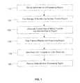
- FIG. 1is a flow chart of a tungsten selective etch process according to disclosed embodiments.
- FIG. 2Ashows a schematic cross-sectional view of a substrate processing chamber according to the disclosed technology.
- FIG. 2Bshows a schematic cross-sectional view of a portion of a substrate processing chamber according to the disclosed technology.
- FIG. 2Cshows a bottom plan view of a showerhead according to the disclosed technology.
- FIG. 3shows a top plan view of an exemplary substrate processing system according to the disclosed technology.
- tungstenrelative to silicon-containing films (e.g. silicon oxide, silicon carbon nitride and (poly)silicon) as well as tungsten oxide are described.
- the methodsinclude a remote plasma etch formed from a fluorine-containing precursor and/or hydrogen (H 2 ). Plasma effluents from the remote plasma are flowed into a substrate processing region where the plasma effluents react with the tungsten. The plasma effluents react with exposed surfaces and selectively remove tungsten while very slowly removing other exposed materials. Sequential and simultaneous methods are included to remove thin tungsten oxide which may, for example, result from exposure to the atmosphere.
- silicon-containing filmse.g. silicon oxide, silicon carbon nitride and (poly)silicon
- H 2hydrogen
- An ion suppression elementmay be included in the etch processes discussed herein in order to achieve high tungsten selectivity.
- the ion suppression elementfunctions to reduce or eliminate ionically charged species traveling from the plasma generation region to the substrate. Uncharged neutral and radical species may pass through the openings in the ion suppressor to react at the substrate.
- the ion suppressorhelps control the concentration of ionic species in the reaction region at a level that assists the process.
- an ion suppressor as described in the exemplary equipment sectionmay be used to provide radical and/or neutral species for selectively etching substrates.
- an ion suppressoris used to provide fluorine-containing plasma effluents to selectively etch tungsten.
- the ion suppressormay be used to provide a reactive gas having a higher concentration of radicals than ions. Because most of the charged particles of a plasma are filtered or removed by the ion suppressor, the substrate is not necessarily biased during the etch process.
- Such a process using radicals and other neutral speciescan reduce plasma damage compared to conventional plasma etch processes that include sputtering and bombardment.
- Embodiments of the present inventionare also advantageous over conventional wet etch processes where surface tension of liquids can cause bending and peeling of small features.
- FIG. 1is a flow chart of a tungsten selective etch process according to disclosed embodiments.
- the tungstenmay also have a thin native oxide layer on its surface due to atmospheric exposure.
- the tungstenmay be in the form of a blanket layer on the substrate or it may reside in discrete regions of a patterned substrate surface. In either case, the tungsten forms exposed surfaces of the surface of the substrate.
- the substrateis then delivered into a processing region (operation 110 ).
- a thin layer of tungsten oxidemay be present over the otherwise exposed tungsten regions of the substrate prior to delivering the substrate into the processing region, after delivering the substrate to the processing region, for example, by treating exposed regions of tungsten to a reactive oxygen source.
- a flow of nitrogen trifluorideis introduced into a plasma region separate from the processing region (operation 120 ).
- Other sources of fluorinemay be used to augment or replace the nitrogen trifluoride.
- a fluorine-containing precursormay be flowed into the plasma region and the fluorine-containing precursor comprises at least one precursor selected from the group consisting of atomic fluorine, diatomic fluorine, bromine trifluoride, chlorine trifluoride, nitrogen trifluoride, hydrogen fluoride, sulfur hexafluoride and xenon difluoride.
- the inventorshave observed higher etch rates for all embodiments disclosed herein when using nitrogen trifluoride in the mix of precursors delivered to the remote plasma region.
- the inventorsconjecture that nitrogen trifluoride plasma effluents experience a significantly longer excited lifetime prior to deexcitation and/or recombination.
- the extended lifetimeallows etch species to travel from remote plasma region into the vicinity of the substrate prior to deexcitation/recombination.
- the separate plasma regionmay be referred to as a remote plasma region herein and may be within a distinct module from the processing chamber or a compartment within the processing chamber.
- a carbon-and-hydrogen-containing precursorin this case methyl fluoride (CH 3 F) is also flowed into the plasma region (operation 125 ) where it is simultaneously excited in a plasma along with the nitrogen trifluoride.
- the flow rate of the atomic hydrogenmay be greater than the flow rate of the atomic fluorine in order to maintain a removal rate of tungsten.
- fluorine contributionscome from both the carbon source and the nitrogen trifluoride. The contribution from each precursor must be considered in order to calculate the H:F atomic flow ratio.
- the plasma effluents formed in the remote plasma regionare then flowed into the substrate processing region (operation 130 ).
- Tungsten on the substrateis selectively etched (operation 135 ) such that tungsten may be removed more rapidly than a variety of other materials.
- the selective etch disclosed in all examples disclosed hereinmay etch tungsten significantly faster than one of tungsten oxide, titanium nitride or a silicon-containing material such as silicon (e.g. polysilicon), silicon oxide, silicon nitride or silicon carbon nitride in embodiments of the invention.
- Such a processmay have broad-based utility, but may find clear utility in removing a layer of tungsten gapfill used to fill small high aspect ratio trenches (such as may be used to form a temporary separator between vertically integrated memory sub-elements).
- the inventionmay involve maintenance of an atomic flow ratio of fluorine (F) to hydrogen (H) in order achieve high etch selectivity of tungsten.
- fluorine and hydrogenare thought to enable two reactions to proceed: (1) one which consumes hydrogen (from CH 3 F) to convert native tungsten oxide to tungsten by shedding moisture through the exhaust system and (2) another reaction which consumes fluorine to remove tungsten in the form of exhausted tungsten hexafluoride (WF 6 ).
- H:Fatomic flow ratio
- An atomic gas flow ratio (H:F) less than or about 15:1, less than or about 12:1, less than or about 10:1 or less than or about 7:1is used, in embodiments of the invention, to achieve favorable selectivities.
- the inventorshave also found that selective dry etches described herein can achieve favorable selectivities without any hydrogen component when not native oxide is present on a tungsten surface.
- the etch selectivity (tungsten:secondary material other than tungsten) of the processes disclosed hereinmay be greater than or about 10:1, greater than or about 20:1, greater than or about 50:1, or greater than or about 100:1 for materials other than in embodiments of the invention.
- the inventorshave found that the processes disclosed herein display etch selectivities of tungsten relative to a variety of specific materials.
- the etch selectivity of tungsten relative to (poly)siliconmay be greater than or about 100:1, greater than or about 150:1, greater than or about 200:1 or greater than or about 250:1 in disclosed embodiments.
- the etch selectivity of tungsten relative to silicon oxidemay be greater than or about 15:1, greater than or about 25:1, greater than or about 30:1 or greater than or about 40:1 in embodiments of the invention.
- the etch selectivity of tungsten relative to silicon carbon nitridemay be greater than or about 3:1, greater than or about 5:1, greater than or about 7:1 or greater than or about 10:1 in embodiments of the invention.
- the etch selectivity of tungsten relative to tungsten oxidemay be greater than or about 10:1, greater than or about 20:1, greater than or about 50:1 or greater than or about 100:1 in embodiments of the invention.
- the flows of the fluorine-containing precursor and the carbon-and-hydrogen-containing precursormay further include one or more relatively inert gases such as He, N 2 , Ar.
- the inert gascan be used to improve plasma stability, process uniformity and the like.
- Argonis helpful, as an additive, to promote the formation of a stable plasma. Process uniformity is generally increased when helium is included.
- Flow rates and ratios of the different gasesmay be used to control etch rates and etch selectivity.
- the fluorine-containing gas(e.g. NF 3 ) is supplied at a flow rate of between about 25 sccm (standard cubic centimeters per minute) and 400 sccm, CH 3 F at a flow rate of between about 50 sccm and 600 sccm, He at a flow rate of between about 0 slm (standard liters per minute) and 3 slm, and Ar at a flow rate of between about 0 slm and 3 slm.
- gases and/or flowsmay be used depending on a number of factors including processing chamber configuration, substrate size, geometry and layout of features being etched, and the like.
- a flow of hydrogen (H 2 ) into the remote plasma regioncan lessen the flow rate requirement for methyl fluoride.
- the inventorshave also found that flowing a combination of hydrogen (H 2 ) and carbon tetrafluoride (CF 4 ) is a productive replacement of CH 3 F, CH 2 F 2 or CHF 3 as well as precursors of the general form CxHyFz, in other words partially fluorinated hydrocarbons. Therefore, a carbon-and-hydrogen-containing precursor, as recited herein, includes a flow of a hydrogen-containing precursor and carbon-containing precursor into the remote plasma region in disclosed embodiments.
- the methodalso includes applying energy to the fluorine-containing precursor and the carbon-and-hydrogen-containing precursor (CH 3 F) while they are in the remote plasma region to generate the plasma effluents.
- the plasmamay include a number of charged and neutral species including radicals and ions.
- the plasmamay be generated using known techniques (e.g., radio frequency excitations, capacitively-coupled power, inductively coupled power, and the like).
- the energyis applied using a capacitively-coupled plasma unit.
- the remote plasma source powermay be between about 40 watts and about 500 watts, between about 75 watts and about 400 watts, between about 150 watts and about 350 watts, or between about 200 watts and about 300 watts in embodiments of the invention.
- the narrowest RF power embodimentoptimizes the selective removal of tungsten relative to a variety of other exposed materials including silicon carbon nitride.
- the pressure in the remote plasma regionmay be such that the pressure in the substrate processing region ends up between about 0.01 Torr and about 50 Torr or between about 0.1 Torr and about 5 Torr in disclosed embodiments.
- the capacitively-coupled plasma unitmay be disposed remote from a gas reaction region of the processing chamber. For example, the capacitively-coupled plasma unit and the plasma generation region may be separated from the gas reaction region by a showerhead.
- the temperature of the substrate during this first examplemay be between about ⁇ 30° C. and about 400° C. in general. In embodiments, the temperature of the substrate during the dry etches described in this section may be greater than or about ⁇ 30° C., greater than or about ⁇ 10° C., greater than or about 10° C., or greater than or about 25° C.
- the substrate temperaturesmay be less than or about 400° C., less than or about 350° C., less than or about 250° C. in disclosed embodiments.
- the etch rate of tungstenwas found to rise with increased substrate temperature (from about 10° C. up through 100° C.) but using lower temperatures was helpful for achieving high selectivities by suppressing, for example, the etch rate of tungsten oxide.
- An additional stepmay be included (prior to operations 120 - 135 ) by providing a flow of hydrogen (H 2 ) to the remote plasma region.
- the plasma effluents produced from the excited molecular hydrogen (H 2 )has been found by the inventors to remove, presumably, the oxygen from the native tungsten oxide. The net effect was that this additional step exposed a predominantly tungsten region to the further processing depicted in FIG. 1 .
- the addition of a fluorine-containing precursor to the remote plasma region during this stepis optional, in part, because of the thinness of native oxides formed when tungsten is exposed to atmosphere.
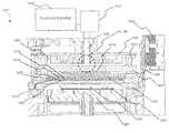
- FIG. 2Ashows a cross-sectional view of an exemplary substrate processing chamber 1001 with partitioned plasma generation regions within the processing chamber.
- film etchinge.g., titanium nitride, tantalum nitride, tungsten, silicon, polysilicon, silicon oxide, silicon nitride, silicon oxynitride, silicon oxycarbide, etc.
- a process gasmay be flowed into chamber plasma region 1015 through a gas inlet assembly 1005 .
- a remote plasma system (RPS) 1002may optionally be included in the system, and may process a first gas which then travels through gas inlet assembly 1005 .
- RPSremote plasma system
- the inlet assembly 1005may include two or more distinct gas supply channels where the second channel (not shown) may bypass the RPS 1002 , if included. Accordingly, in disclosed embodiments the precursor gases may be delivered to the processing chamber in an unexcited state. In another example, the first channel provided through the RPS may be used for the process gas and the second channel bypassing the RPS may be used for a treatment gas in disclosed embodiments.
- the process gasmay be excited within the RPS 1002 prior to entering the chamber plasma region 1015 . Accordingly, the fluorine-containing precursor as discussed above, for example, may pass through RPS 1002 or bypass the RPS unit in disclosed embodiments. Various other examples encompassed by this arrangement will be similarly understood.
- a cooling plate 1003 , faceplate 1017 , ion suppressor 1023 , showerhead 1025 , and a substrate support 1065(also known as a pedestal), having a substrate 1055 disposed thereon, are shown and may each be included according to disclosed embodiments.
- the pedestal 1065may have a heat exchange channel through which a heat exchange fluid flows to control the temperature of the substrate. This configuration may allow the substrate 1055 temperature to be cooled or heated to maintain relatively low temperatures, such as between about ⁇ 20° C. to about 200° C., or therebetween.
- the heat exchange fluidmay comprise ethylene glycol and/or water.
- the wafer support platter of the pedestal 1065which may comprise aluminum, ceramic, or a combination thereof, may also be resistively heated in order to achieve relatively high temperatures, such as from up to or about 100° C. to above or about 1100° C., using an embedded resistive heater element.
- the heating elementmay be formed within the pedestal as one or more loops, and an outer portion of the heater element may run adjacent to a perimeter of the support platter, while an inner portion runs on the path of a concentric circle having a smaller radius.
- the wiring to the heater elementmay pass through the stem of the pedestal 1065 , which may be further configured to rotate.
- the faceplate 1017may be pyramidal, conical, or of another similar structure with a narrow top portion expanding to a wide bottom portion.
- the faceplate 1017may additionally be flat as shown and include a plurality of through-channels used to distribute process gases. Plasma generating gases and/or plasma excited species, depending on use of the RPS 1002 , may pass through a plurality of holes, shown in FIG. 2B , in faceplate 1017 for a more uniform delivery into the chamber plasma region 1015 .
- Exemplary configurationsmay include having the gas inlet assembly 1005 open into a gas supply region 1058 partitioned from the chamber plasma region 1015 by faceplate 1017 so that the gases/species flow through the holes in the faceplate 1017 into the chamber plasma region 1015 .
- Structural and operational featuresmay be selected to prevent significant backflow of plasma from the chamber plasma region 1015 back into the supply region 1058 , gas inlet assembly 1005 , and fluid supply system 1010 .
- the structural featuresmay include the selection of dimensions and cross-sectional geometries of the apertures in faceplate 1017 to deactivate back-streaming plasma.
- the operational featuresmay include maintaining a pressure difference between the gas supply region 1058 and chamber plasma region 1015 that maintains a unidirectional flow of plasma through the showerhead 1025 .
- the faceplate 1017 , or a conductive top portion of the chamber, and showerhead 1025are shown with an insulating ring 1020 located between the features, which allows an AC potential to be applied to the faceplate 1017 relative to showerhead 1025 and/or ion suppressor 1023 .
- the insulating ring 1020may be positioned between the faceplate 1017 and the showerhead 1025 and/or ion suppressor 1023 enabling a capacitively coupled plasma (CCP) to be formed in the first plasma region.
- a baffle(not shown) may additionally be located in the chamber plasma region 1015 , or otherwise coupled with gas inlet assembly 1005 , to affect the flow of fluid into the region through gas inlet assembly 1005 .
- the ion suppressor 1023may comprise a plate or other geometry that defines a plurality of apertures throughout the structure that are configured to suppress the migration of ionically-charged species out of chamber plasma region 1015 while allowing uncharged neutral or radical species to pass through the ion suppressor 1023 into an activated gas delivery region between the suppressor and the showerhead.
- the ion suppressor 1023may comprise a perforated plate with a variety of aperture configurations. These uncharged species may include highly reactive species that are transported with less reactive carrier gas through the apertures. As noted above, the migration of ionic species through the holes may be reduced, and in some instances completely suppressed.
- Controlling the amount of ionic species passing through the ion suppressor 1023may provide increased control over the gas mixture brought into contact with the underlying wafer substrate, which in turn may increase control of the deposition and/or etch characteristics of the gas mixture.
- adjustments in the ion concentration of the gas mixturecan significantly alter its etch selectivity, e.g., W:WOx etch ratios, W:SiCN etch ratios, etc.
- itcan also shift the balance of conformal-to-flowable style depositions for dielectric materials.
- the plurality of holes in the ion suppressor 1023may be configured to control the passage of the activated gas, i.e., the ionic, radical, and/or neutral species, through the ion suppressor 1023 .
- the aspect ratio of the holes, or the hole diameter to length, and/or the geometry of the holesmay be controlled so that the flow of ionically-charged species in the activated gas passing through the ion suppressor 1023 is reduced.
- the holes in the ion suppressor 1023may include a tapered portion that faces chamber plasma region 1015 , and a cylindrical portion that faces the showerhead 1025 .
- the cylindrical portionmay be shaped and dimensioned to control the flow of ionic species passing to the showerhead 1025 .
- An adjustable electrical biasmay also be applied to the ion suppressor 1023 as an additional means to control the flow of ionic species through the suppressor.
- the ion suppression element 1023may function to reduce or eliminate the amount of ionically charged species traveling from the plasma generation region to the substrate. Uncharged neutral and radical species may still pass through the openings in the ion suppressor to react with the substrate. It should be noted that the complete elimination of ionically charged species in the reaction region surrounding the substrate is not always the desired goal. In many instances, ionic species are required to reach the substrate in order to perform the etch and/or deposition process. In these instances, the ion suppressor may help to control the concentration of ionic species in the reaction region at a level that assists the process.
- showerhead 1025 in combination with ion suppressor 1023may allow a plasma present in chamber plasma region 1015 to avoid directly exciting gases in substrate processing region 1033 , while still allowing excited species to travel from chamber plasma region 1015 into substrate processing region 1033 .
- the chambermay be configured to prevent the plasma from contacting a substrate 1055 being etched. This may advantageously protect a variety of intricate structures and films patterned on the substrate, which may be damaged, dislocated, or otherwise warped if directly contacted by a generated plasma.
- the rate at which oxide species etchmay increase. Accordingly, if the exposed second material is oxide, this material may be further protected by maintaining the plasma remotely from the substrate.
- the processing systemmay further include a power supply 1040 electrically coupled with the processing chamber to provide electric power to the faceplate 1017 , ion suppressor 1023 , showerhead 1025 , and/or pedestal 1065 to generate a plasma in the chamber plasma region 1015 or processing region 1033 .
- the power supplymay be configured to deliver an adjustable amount of power to the chamber depending on the process performed. Such a configuration may allow for a tunable plasma to be used in the processes being performed. Unlike a remote plasma unit, which is often presented with on or off functionality, a tunable plasma may be configured to deliver a specific amount of power to chamber plasma region 1015 . This in turn may allow development of particular plasma characteristics such that precursors may be dissociated in specific ways to enhance the etching profiles produced by these precursors.
- a plasmamay be ignited either in chamber plasma region 1015 above showerhead 1025 or substrate processing region 1033 below showerhead 1025 .
- a plasmamay be present in chamber plasma region 1015 to produce the radical-fluorine precursors from an inflow of the fluorine-containing precursor.
- An AC voltage typically in the radio frequency (RF) rangemay be applied between the conductive top portion of the processing chamber, such as faceplate 1017 , and showerhead 1025 and/or ion suppressor 1023 to ignite a plasma in chamber plasma region 1015 during deposition.
- An RF power supplymay generate a high RF frequency of 13.56 MHz but may also generate other frequencies alone or in combination with the 13.56 MHz frequency.
- Plasma powercan be of a variety of frequencies or a combination of multiple frequencies.
- the plasmamay be provided by RF power delivered to faceplate 1017 relative to ion suppressor 1023 and/or showerhead 1025 .
- the RF powermay be between about 10 watts and about 2000 watts, between about 100 watts and about 2000 watts, between about 200 watts and about 1500 watts, or between about 200 watts and about 1000 watts in different embodiments.
- the RF frequency applied in the exemplary processing systemmay be low RF frequencies less than about 200 kHz, high RF frequencies between about 10 MHz and about 15 MHz, or microwave frequencies greater than or about 1 GHz in different embodiments.
- the plasma powermay be capacitively-coupled (CCP) or inductively-coupled (ICP) into the remote plasma region.
- CCPcapacitively-coupled
- ICPinductively-coupled
- Chamber plasma region 1015may be left at low or no power when a bottom plasma in the substrate processing region 1033 is turned on to, for example, cure a film or clean the interior surfaces bordering substrate processing region 1033 .
- a plasma in substrate processing region 1033may be ignited by applying an AC voltage between showerhead 1055 and the pedestal 1065 or bottom of the chamber.
- a cleaning gasmay be introduced into substrate processing region 1033 while the plasma is present.
- a fluidsuch as a precursor, for example a fluorine-containing precursor
- a precursorfor example a fluorine-containing precursor
- Excited species derived from the process gas in chamber plasma region 1015may travel through apertures in the ion suppressor 1023 , and/or showerhead 1025 and react with an additional precursor flowing into the processing region 1033 from a separate portion of the showerhead.
- no additional precursorsmay be flowed through the separate portion of the showerhead. Little or no plasma may be present in the processing region 1033 .
- Excited derivatives of the precursorsmay combine in the region above the substrate and, on occasion, on the substrate to etch structures or remove species on the substrate in disclosed applications.
- Exciting the fluids in the chamber plasma region 1015 directly, or exciting the fluids in the RPS units 1002may provide several benefits.
- the concentration of the excited species derived from the fluidsmay be increased within the processing region 1033 due to the plasma in the chamber plasma region 1015 . This increase may result from the location of the plasma in the chamber plasma region 1015 .
- the processing region 1033may be located closer to the chamber plasma region 1015 than the remote plasma system (RPS) 1002 , leaving less time for the excited species to leave excited states through collisions with other gas molecules, walls of the chamber, and surfaces of the showerhead.
- RPSremote plasma system
- the uniformity of the concentration of the excited species derived from the process gasmay also be increased within the processing region 1033 . This may result from the shape of the chamber plasma region 1015 , which may be more similar to the shape of the processing region 1033 . Excited species created in the RPS 1002 may travel greater distances in order to pass through apertures near the edges of the showerhead 1025 relative to species that pass through apertures near the center of the showerhead 1025 . The greater distance may result in a reduced excitation of the excited species and, for example, may result in a slower growth rate near the edge of a substrate. Exciting the fluids in the chamber plasma region 1015 may mitigate this variation for the fluid flowed through RPS 1002 , or alternatively bypassed around the RPS unit.
- the processing gasesmay be excited in chamber plasma region 1015 and may be passed through the showerhead 1025 to the processing region 1033 in the excited state. While a plasma may be generated in the processing region 1033 , a plasma may alternatively not be generated in the processing region.
- the only excitation of the processing gas or precursorsmay be from exciting the processing gases in chamber plasma region 1015 to react with one another in the processing region 1033 . As previously discussed, this may be to protect the structures patterned on the substrate 1055 .
- a treatment gasmay be introduced to remove unwanted species from the chamber walls, the substrate, the deposited film and/or the film during deposition.
- a treatment gasmay be excited in a plasma and then used to reduce or remove residual content inside the chamber. In other disclosed embodiments the treatment gas may be used without a plasma.
- the deliverymay be achieved using a mass flow meter (MFM), an injection valve, or by commercially available water vapor generators.
- MFMmass flow meter
- the treatment gasmay be introduced to the processing region 1033 , either through the RPS unit or bypassing the RPS unit, and may further be excited in the first plasma region.
- FIG. 2Bshows a detailed view of the features affecting the processing gas distribution through faceplate 1017 .
- faceplate 1017 , cooling plate 1003 , and gas inlet assembly 1005intersect to define a gas supply region 1058 into which process gases may be delivered from gas inlet 1005 .
- the gasesmay fill the gas supply region 1058 and flow to chamber plasma region 1015 through apertures 1059 in faceplate 1017 .
- the apertures 1059may be configured to direct flow in a substantially unidirectional manner such that process gases may flow into processing region 1033 , but may be partially or fully prevented from backflow into the gas supply region 1058 after traversing the faceplate 1017 .
- the gas distribution assemblies such as showerhead 1025 for use in the processing chamber section 1001may be referred to as dual channel showerheads (DCSH) and are additionally detailed in the embodiments described in FIG. 2A as well as FIG. 2C herein.
- the dual channel showerheadmay provide for etching processes that allow for separation of etchants outside of the processing region 1033 to provide limited interaction with chamber components and each other prior to being delivered into the processing region.
- the showerhead 1025may comprise an upper plate 1014 and a lower plate 1016 .
- the platesmay be coupled with one another to define a volume 1018 between the plates.
- the coupling of the platesmay be so as to provide first fluid channels 1019 through the upper and lower plates, and second fluid channels 1021 through the lower plate 1016 .
- the formed channelsmay be configured to provide fluid access from the volume 1018 through the lower plate 1016 via second fluid channels 1021 alone, and the first fluid channels 1019 may be fluidly isolated from the volume 1018 between the plates and the second fluid channels 1021 .
- the volume 1018may be fluidly accessible through a side of the gas distribution assembly 1025 .
- FIG. 2includes a dual-channel showerhead, it is understood that alternative distribution assemblies may be utilized that maintain first and second precursors fluidly isolated prior to the processing region 1033 .
- a perforated plate and tubes underneath the platemay be utilized, although other configurations may operate with reduced efficiency or not provide as uniform processing as the dual-channel showerhead as described.
- showerhead 1025may distribute via first fluid channels 1019 process gases which contain plasma effluents upon excitation by a plasma in chamber plasma region 1015 .
- the process gas introduced into the RPS 1002 and/or chamber plasma region 1015may contain fluorine, e.g., CF 4 , NF 3 or XeF 2 .
- the process gasmay also include a carrier gas such as helium, argon, nitrogen (N 2 ), etc.
- Plasma effluentsmay include ionized or neutral derivatives of the process gas and may also be referred to herein as a radical-fluorine precursor referring to the atomic constituent of the process gas introduced.
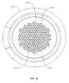
- FIG. 2Cis a bottom view of a showerhead 1025 for use with a processing chamber according to disclosed embodiments.
- showerhead 1025corresponds with the showerhead shown in FIG. 2A .
- Through-holes 1031which show a view of first fluid channels 1019 , may have a plurality of shapes and configurations in order to control and affect the flow of precursors through the showerhead 1025 .
- Small holes 1027which show a view of second fluid channels 1021 , may be distributed substantially evenly over the surface of the showerhead, even amongst the through-holes 1031 , which may help to provide more even mixing of the precursors as they exit the showerhead than other configurations.
- the chamber plasma region 1015 or a region in an RPSmay be referred to as a remote plasma region.
- the radical precursore.g., a radical-fluorine precursor
- the additional precursorsare excited only by the radical-fluorine precursor.
- Plasma powermay essentially be applied only to the remote plasma region in embodiments to ensure that the radical-fluorine precursor provides the dominant excitation.
- Nitrogen trifluoride or another fluorine-containing precursormay be flowed into chamber plasma region 1015 at rates between about 25 sccm and about 500 sccm, between about 50 sccm and about 150 sccm, or between about 75 sccm and about 125 sccm in disclosed embodiments.
- Methyl fluoride or another partially fluorinated hydro-carbonmay be flowed with a flowrate that results in an atomic H:F flow rate ratio of greater than, for example, 1:1.
- Combined flow rates of precursors into the chambermay account for 0.05% to about 20% by volume of the overall gas mixture; the remainder being carrier gases.
- the fluorine-containing precursormay be flowed into the remote plasma region, but the plasma effluents may have the same volumetric flow ratio in embodiments.
- a purge or carrier gasmay be first initiated into the remote plasma region before the fluorine-containing gas to stabilize the pressure within the remote plasma region.
- Substrate processing region 1033can be maintained at a variety of pressures during the flow of precursors, any carrier gases, and plasma effluents into substrate processing region 1033 .
- the pressuremay be maintained between about 0.1 mTorr and about 100 Torr, between about 1 Torr and about 20 Torr or between about 1 Torr and about 5 Torr in different embodiments.
- FIG. 3shows one such processing system 1101 of deposition, etching, baking, and curing chambers according to disclosed embodiments.
- a pair of front opening unified pods(load lock chambers 1102 ) supply substrates of a variety of sizes that are received by robotic arms 1104 and placed into a low pressure holding area 1106 before being placed into one of the substrate processing chambers 1108 a - f .
- a second robotic arm 1110may be used to transport the substrate wafers from the holding area 1106 to the substrate processing chambers 1108 a - f and back.
- Each substrate processing chamber 1108 a - fcan be outfitted to perform a number of substrate processing operations including the dry etch processes described herein in addition to cyclical layer deposition (CLD), atomic layer deposition (ALD), chemical vapor deposition (CVD), physical vapor deposition (PVD), etch, pre-clean, degas, orientation, and other substrate processes.
- CLDcyclical layer deposition
- ALDatomic layer deposition
- CVDchemical vapor deposition
- PVDphysical vapor deposition
- etchpre-clean, degas, orientation, and other substrate processes.
- the substrate processing chambers 1108 a - fmay include one or more system components for depositing, annealing, curing and/or etching a dielectric film on the substrate wafer.
- two pairs of the processing chambere.g., 1108 c - d and 1108 e - f
- the third pair of processing chamberse.g., 1108 a - b
- all three pairs of chamberse.g., 1108 a - f
- Any one or more of the processes describedmay be carried out in chamber(s) separated from the fabrication system shown in different embodiments.
- substratemay be a support substrate with or without layers formed thereon.
- the patterned substratemay be an insulator or a semiconductor of a variety of doping concentrations and profiles and may, for example, be a semiconductor substrate of the type used in the manufacture of integrated circuits.
- siliconof the patterned substrate is predominantly Si but may include minority concentrations of other elemental constituents such as nitrogen, oxygen, hydrogen, carbon and the like.
- tungstenof the patterned substrate is predominantly W but may include minority concentrations of other elemental constituents such as nitrogen, oxygen, hydrogen, carbon and the like. Of course, “exposed tungsten” may consist of only tungsten.
- Exposed “silicon nitride” of the patterned substrateis predominantly Si 3 N 4 but may include minority concentrations of other elemental constituents such as oxygen, hydrogen, carbon and the like. “Exposed silicon nitride” may consist only of silicon and nitrogen. Exposed “silicon oxide” of the patterned substrate is predominantly SiO 2 but may include minority concentrations of other elemental constituents such as nitrogen, hydrogen, carbon and the like. In some embodiments, silicon oxide films etched using the methods disclosed herein consist of silicon and oxygen. “Tungsten oxide” is predominantly tungsten and oxygen but may include minority concentrations of other elemental constituents such as nitrogen, hydrogen, carbon and the like. Tungsten oxide may consist of tungsten and oxygen. “Titanium nitride” is predominantly titanium and nitrogen but may include minority concentrations of other elemental constituents such as nitrogen, hydrogen, carbon and the like. Titanium nitride may consist of titanium and nitrogen.
- plasma effluentsdescribe gas exiting from the chamber plasma region and entering the substrate processing region. Plasma effluents are in an “excited state” wherein at least some of the gas molecules are in vibrationally-excited, dissociated and/or ionized states.
- a “radical precursor”is used to describe plasma effluents (a gas in an excited state which is exiting a plasma) which participate in a reaction to either remove material from or deposit material on a surface.
- Radar-fluorine(or “radical-hydrogen”) are radical precursors which contain fluorine (or hydrogen) but may contain other elemental constituents.
- inert gasrefers to any gas which does not form chemical bonds when etching or being incorporated into a film. Exemplary inert gases include noble gases but may include other gases so long as no chemical bonds are formed when (typically) trace amounts are trapped in a film.
- trench and trenchare used throughout with no implication that the etched geometry has a large horizontal aspect ratio. Viewed from above the surface, trenches may appear circular, oval, polygonal, rectangular, or a variety of other shapes. A trench may be in the shape of a moat around an island of material.
- viais used to refer to a low aspect ratio trench (as viewed from above) which may or may not be filled with metal to form a vertical electrical connection.
- a conformal etch processrefers to a generally uniform removal of material on a surface in the same shape as the surface, i.e., the surface of the etched layer and the pre-etch surface are generally parallel. A person having ordinary skill in the art will recognize that the etched interface likely cannot be 100% conformal and thus the term “generally” allows for acceptable tolerances.
Landscapes
- Engineering & Computer Science (AREA)
- Physics & Mathematics (AREA)
- Plasma & Fusion (AREA)
- Computer Hardware Design (AREA)
- Condensed Matter Physics & Semiconductors (AREA)
- General Physics & Mathematics (AREA)
- Manufacturing & Machinery (AREA)
- Microelectronics & Electronic Packaging (AREA)
- Power Engineering (AREA)
- Chemical & Material Sciences (AREA)
- Chemical Kinetics & Catalysis (AREA)
- General Chemical & Material Sciences (AREA)
- Analytical Chemistry (AREA)
- Drying Of Semiconductors (AREA)
Abstract
Description
This application claims the benefit of U.S. Provisional Application No. 61/753,677 by Wang et al, filed Jan. 17, 2013, and titled “DRY-ETCH FOR SELECTIVE TUNGSTEN REMOVAL.” This application also claims the benefit of U.S. Provisional Application No. 61/732,074 by Kim et al, filed Nov. 30, 2012 and titled “DRY-ETCH FOR SELECTIVE OXIDATION REMOVAL.” Each of the above U.S. Provisional Applications is incorporated herein in its entirety for all purposes.
Integrated circuits are made possible by processes which produce intricately patterned material layers on substrate surfaces. Producing patterned material on a substrate requires controlled methods for removal of exposed material. Chemical etching is used for a variety of purposes including transferring a pattern in photoresist into underlying layers, thinning layers or thinning lateral dimensions of features already present on the surface. Often it is desirable to have an etch process which etches one material faster than another helping e.g. a pattern transfer process proceed. Such an etch process is said to be selective to the first material. As a result of the diversity of materials, circuits and processes, etch processes have been developed with a selectivity towards a variety of materials. However, there are few options for selectively etching metals.
Dry etch processes are often desirable for selectively removing material from semiconductor substrates. The desirability stems from the ability to gently remove material from miniature structures with minimal physical disturbance. Dry etch processes also allow the etch rate to be abruptly stopped by removing the gas phase reagents. Some dry-etch processes involve the exposure of a substrate to remote plasma by-products formed from one or more precursors. For example, remote plasma excitation of ammonia and nitrogen trifluoride enables silicon oxide to be selectively removed from a patterned substrate when the plasma effluents are flowed into the substrate processing region. Remote plasma etch processes have recently been developed to selectively remove a variety of dielectrics relative to one another. However, fewer dry-etch processes have been developed to selectively remove metals and their native oxidation.
Methods are needed to selectively and delicately etch exposed metal surfaces.
Methods of selectively etching tungsten relative to silicon-containing films (e.g. silicon oxide, silicon carbon nitride and (poly)silicon) as well as tungsten oxide are described. The methods include a remote plasma etch formed from a fluorine-containing precursor and/or hydrogen (H2). Plasma effluents from the remote plasma are flowed into a substrate processing region where the plasma effluents react with the tungsten. The plasma effluents react with exposed surfaces and selectively remove tungsten while very slowly removing other exposed materials. Sequential and simultaneous methods are included to remove thin tungsten oxide which may, for example, result from exposure to the atmosphere.
Embodiments of the invention include methods of etching a patterned substrate in a substrate processing region of a substrate processing chamber. The patterned substrate has a exposed tungsten region and an exposed second material region. The methods include flowing a fluorine-containing precursor into a remote plasma region fluidly coupled to the substrate processing region while forming a plasma in the plasma region to produce plasma effluents. The methods further include etching the exposed tungsten from the substrate by flowing the plasma effluents into the substrate processing region through through-holes in a showerhead.
Additional embodiments and features are set forth in part in the description that follows, and in part will become apparent to those skilled in the art upon examination of the specification or may be learned by the practice of the disclosed embodiments. The features and advantages of the disclosed embodiments may be realized and attained by means of the instrumentalities, combinations, and methods described in the specification.
A further understanding of the nature and advantages of the disclosed embodiments may be realized by reference to the remaining portions of the specification and the drawings.
In the appended figures, similar components and/or features may have the same reference label. Further, various components of the same type may be distinguished by following the reference label by a dash and a second label that distinguishes among the similar components. If only the first reference label is used in the specification, the description is applicable to any one of the similar components having the same first reference label irrespective of the second reference label.
Methods of selectively etching tungsten relative to silicon-containing films (e.g. silicon oxide, silicon carbon nitride and (poly)silicon) as well as tungsten oxide are described. The methods include a remote plasma etch formed from a fluorine-containing precursor and/or hydrogen (H2). Plasma effluents from the remote plasma are flowed into a substrate processing region where the plasma effluents react with the tungsten. The plasma effluents react with exposed surfaces and selectively remove tungsten while very slowly removing other exposed materials. Sequential and simultaneous methods are included to remove thin tungsten oxide which may, for example, result from exposure to the atmosphere.
An ion suppression element may be included in the etch processes discussed herein in order to achieve high tungsten selectivity. The ion suppression element functions to reduce or eliminate ionically charged species traveling from the plasma generation region to the substrate. Uncharged neutral and radical species may pass through the openings in the ion suppressor to react at the substrate. The ion suppressor helps control the concentration of ionic species in the reaction region at a level that assists the process.
In accordance with some embodiments of the invention, an ion suppressor as described in the exemplary equipment section may be used to provide radical and/or neutral species for selectively etching substrates. In one embodiment, for example, an ion suppressor is used to provide fluorine-containing plasma effluents to selectively etch tungsten. The ion suppressor may be used to provide a reactive gas having a higher concentration of radicals than ions. Because most of the charged particles of a plasma are filtered or removed by the ion suppressor, the substrate is not necessarily biased during the etch process. Such a process using radicals and other neutral species can reduce plasma damage compared to conventional plasma etch processes that include sputtering and bombardment. Embodiments of the present invention are also advantageous over conventional wet etch processes where surface tension of liquids can cause bending and peeling of small features.
In order to better understand and appreciate the invention, reference is now made toFIG. 1 which is a flow chart of a tungsten selective etch process according to disclosed embodiments. The tungsten may also have a thin native oxide layer on its surface due to atmospheric exposure. The tungsten may be in the form of a blanket layer on the substrate or it may reside in discrete regions of a patterned substrate surface. In either case, the tungsten forms exposed surfaces of the surface of the substrate. The substrate is then delivered into a processing region (operation110). A thin layer of tungsten oxide may be present over the otherwise exposed tungsten regions of the substrate prior to delivering the substrate into the processing region, after delivering the substrate to the processing region, for example, by treating exposed regions of tungsten to a reactive oxygen source.
A flow of nitrogen trifluoride is introduced into a plasma region separate from the processing region (operation120). Other sources of fluorine may be used to augment or replace the nitrogen trifluoride. In general, a fluorine-containing precursor may be flowed into the plasma region and the fluorine-containing precursor comprises at least one precursor selected from the group consisting of atomic fluorine, diatomic fluorine, bromine trifluoride, chlorine trifluoride, nitrogen trifluoride, hydrogen fluoride, sulfur hexafluoride and xenon difluoride. However, the inventors have observed higher etch rates for all embodiments disclosed herein when using nitrogen trifluoride in the mix of precursors delivered to the remote plasma region. The inventors conjecture that nitrogen trifluoride plasma effluents experience a significantly longer excited lifetime prior to deexcitation and/or recombination. The extended lifetime allows etch species to travel from remote plasma region into the vicinity of the substrate prior to deexcitation/recombination.
The separate plasma region may be referred to as a remote plasma region herein and may be within a distinct module from the processing chamber or a compartment within the processing chamber. A carbon-and-hydrogen-containing precursor, in this case methyl fluoride (CH3F) is also flowed into the plasma region (operation125) where it is simultaneously excited in a plasma along with the nitrogen trifluoride. The flow rate of the atomic hydrogen may be greater than the flow rate of the atomic fluorine in order to maintain a removal rate of tungsten. In this example, fluorine contributions come from both the carbon source and the nitrogen trifluoride. The contribution from each precursor must be considered in order to calculate the H:F atomic flow ratio. Diatomic hydrogen (H2) may be added as well and is necessary in some instances so that an atomic flow rate ratio greater than H:F=1 is possible.
The plasma effluents formed in the remote plasma region are then flowed into the substrate processing region (operation130). Tungsten on the substrate is selectively etched (operation135) such that tungsten may be removed more rapidly than a variety of other materials. The selective etch disclosed in all examples disclosed herein may etch tungsten significantly faster than one of tungsten oxide, titanium nitride or a silicon-containing material such as silicon (e.g. polysilicon), silicon oxide, silicon nitride or silicon carbon nitride in embodiments of the invention. Such a process may have broad-based utility, but may find clear utility in removing a layer of tungsten gapfill used to fill small high aspect ratio trenches (such as may be used to form a temporary separator between vertically integrated memory sub-elements). The invention may involve maintenance of an atomic flow ratio of fluorine (F) to hydrogen (H) in order achieve high etch selectivity of tungsten. The copresence of fluorine and hydrogen is thought to enable two reactions to proceed: (1) one which consumes hydrogen (from CH3F) to convert native tungsten oxide to tungsten by shedding moisture through the exhaust system and (2) another reaction which consumes fluorine to remove tungsten in the form of exhausted tungsten hexafluoride (WF6). Maintaining an atomic flow ratio (H:F) greater than 1:1, the inventors have found that the collective process is highly selective of tungsten over a variety of other materials including tungsten oxide, despite being capable of removing a thin native tungsten oxide. The reactive chemical species and any process effluents are removed from the substrate processing region and then the substrate is removed from the processing region (operation145).
In disclosed embodiments, an atomic gas flow ratio (H:F) greater than or about 1:1, greater than or about 2:1 or greater than or about 3:1. An atomic gas flow ratio (H:F) less than or about 15:1, less than or about 12:1, less than or about 10:1 or less than or about 7:1 is used, in embodiments of the invention, to achieve favorable selectivities. The inventors have also found that selective dry etches described herein can achieve favorable selectivities without any hydrogen component when not native oxide is present on a tungsten surface. The etch selectivity (tungsten:secondary material other than tungsten) of the processes disclosed herein may be greater than or about 10:1, greater than or about 20:1, greater than or about 50:1, or greater than or about 100:1 for materials other than in embodiments of the invention. The inventors have found that the processes disclosed herein display etch selectivities of tungsten relative to a variety of specific materials. The etch selectivity of tungsten relative to (poly)silicon may be greater than or about 100:1, greater than or about 150:1, greater than or about 200:1 or greater than or about 250:1 in disclosed embodiments. The etch selectivity of tungsten relative to silicon oxide may be greater than or about 15:1, greater than or about 25:1, greater than or about 30:1 or greater than or about 40:1 in embodiments of the invention. The etch selectivity of tungsten relative to silicon carbon nitride may be greater than or about 3:1, greater than or about 5:1, greater than or about 7:1 or greater than or about 10:1 in embodiments of the invention. The etch selectivity of tungsten relative to tungsten oxide may be greater than or about 10:1, greater than or about 20:1, greater than or about 50:1 or greater than or about 100:1 in embodiments of the invention.
The flows of the fluorine-containing precursor and the carbon-and-hydrogen-containing precursor may further include one or more relatively inert gases such as He, N2, Ar. The inert gas can be used to improve plasma stability, process uniformity and the like. Argon is helpful, as an additive, to promote the formation of a stable plasma. Process uniformity is generally increased when helium is included. These additives are present in embodiments throughout this specification. Flow rates and ratios of the different gases may be used to control etch rates and etch selectivity.
In disclosed embodiments, the fluorine-containing gas (e.g. NF3) is supplied at a flow rate of between about 25 sccm (standard cubic centimeters per minute) and 400 sccm, CH3F at a flow rate of between about 50 sccm and 600 sccm, He at a flow rate of between about 0 slm (standard liters per minute) and 3 slm, and Ar at a flow rate of between about 0 slm and 3 slm. One of ordinary skill in the art would recognize that other gases and/or flows may be used depending on a number of factors including processing chamber configuration, substrate size, geometry and layout of features being etched, and the like. Inclusion of a flow of hydrogen (H2) into the remote plasma region can lessen the flow rate requirement for methyl fluoride. The inventors have also found that flowing a combination of hydrogen (H2) and carbon tetrafluoride (CF4) is a productive replacement of CH3F, CH2F2or CHF3as well as precursors of the general form CxHyFz, in other words partially fluorinated hydrocarbons. Therefore, a carbon-and-hydrogen-containing precursor, as recited herein, includes a flow of a hydrogen-containing precursor and carbon-containing precursor into the remote plasma region in disclosed embodiments.
The method also includes applying energy to the fluorine-containing precursor and the carbon-and-hydrogen-containing precursor (CH3F) while they are in the remote plasma region to generate the plasma effluents. As would be appreciated by one of ordinary skill in the art, the plasma may include a number of charged and neutral species including radicals and ions. The plasma may be generated using known techniques (e.g., radio frequency excitations, capacitively-coupled power, inductively coupled power, and the like). In an embodiment, the energy is applied using a capacitively-coupled plasma unit. The remote plasma source power may be between about 40 watts and about 500 watts, between about 75 watts and about 400 watts, between about 150 watts and about 350 watts, or between about 200 watts and about 300 watts in embodiments of the invention. The narrowest RF power embodiment optimizes the selective removal of tungsten relative to a variety of other exposed materials including silicon carbon nitride. The pressure in the remote plasma region may be such that the pressure in the substrate processing region ends up between about 0.01 Torr and about 50 Torr or between about 0.1 Torr and about 5 Torr in disclosed embodiments. The capacitively-coupled plasma unit may be disposed remote from a gas reaction region of the processing chamber. For example, the capacitively-coupled plasma unit and the plasma generation region may be separated from the gas reaction region by a showerhead.
The temperature of the substrate during this first example may be between about −30° C. and about 400° C. in general. In embodiments, the temperature of the substrate during the dry etches described in this section may be greater than or about −30° C., greater than or about −10° C., greater than or about 10° C., or greater than or about 25° C. The substrate temperatures may be less than or about 400° C., less than or about 350° C., less than or about 250° C. in disclosed embodiments. The etch rate of tungsten was found to rise with increased substrate temperature (from about 10° C. up through 100° C.) but using lower temperatures was helpful for achieving high selectivities by suppressing, for example, the etch rate of tungsten oxide.
An additional step may be included (prior to operations120-135) by providing a flow of hydrogen (H2) to the remote plasma region. The plasma effluents produced from the excited molecular hydrogen (H2) has been found by the inventors to remove, presumably, the oxygen from the native tungsten oxide. The net effect was that this additional step exposed a predominantly tungsten region to the further processing depicted inFIG. 1 . The addition of a fluorine-containing precursor to the remote plasma region during this step is optional, in part, because of the thinness of native oxides formed when tungsten is exposed to atmosphere.
Additional process parameters are disclosed in the course of describing an exemplary processing chamber and system.
Exemplary Processing System
Acooling plate 1003,faceplate 1017,ion suppressor 1023,showerhead 1025, and a substrate support1065 (also known as a pedestal), having asubstrate 1055 disposed thereon, are shown and may each be included according to disclosed embodiments. Thepedestal 1065 may have a heat exchange channel through which a heat exchange fluid flows to control the temperature of the substrate. This configuration may allow thesubstrate 1055 temperature to be cooled or heated to maintain relatively low temperatures, such as between about −20° C. to about 200° C., or therebetween. The heat exchange fluid may comprise ethylene glycol and/or water. The wafer support platter of thepedestal 1065, which may comprise aluminum, ceramic, or a combination thereof, may also be resistively heated in order to achieve relatively high temperatures, such as from up to or about 100° C. to above or about 1100° C., using an embedded resistive heater element. The heating element may be formed within the pedestal as one or more loops, and an outer portion of the heater element may run adjacent to a perimeter of the support platter, while an inner portion runs on the path of a concentric circle having a smaller radius. The wiring to the heater element may pass through the stem of thepedestal 1065, which may be further configured to rotate.
Thefaceplate 1017 may be pyramidal, conical, or of another similar structure with a narrow top portion expanding to a wide bottom portion. Thefaceplate 1017 may additionally be flat as shown and include a plurality of through-channels used to distribute process gases. Plasma generating gases and/or plasma excited species, depending on use of theRPS 1002, may pass through a plurality of holes, shown inFIG. 2B , infaceplate 1017 for a more uniform delivery into thechamber plasma region 1015.
Exemplary configurations may include having thegas inlet assembly 1005 open into agas supply region 1058 partitioned from thechamber plasma region 1015 byfaceplate 1017 so that the gases/species flow through the holes in thefaceplate 1017 into thechamber plasma region 1015. Structural and operational features may be selected to prevent significant backflow of plasma from thechamber plasma region 1015 back into thesupply region 1058,gas inlet assembly 1005, andfluid supply system 1010. The structural features may include the selection of dimensions and cross-sectional geometries of the apertures infaceplate 1017 to deactivate back-streaming plasma. The operational features may include maintaining a pressure difference between thegas supply region 1058 andchamber plasma region 1015 that maintains a unidirectional flow of plasma through theshowerhead 1025. Thefaceplate 1017, or a conductive top portion of the chamber, andshowerhead 1025 are shown with an insulatingring 1020 located between the features, which allows an AC potential to be applied to thefaceplate 1017 relative toshowerhead 1025 and/orion suppressor 1023. The insulatingring 1020 may be positioned between thefaceplate 1017 and theshowerhead 1025 and/orion suppressor 1023 enabling a capacitively coupled plasma (CCP) to be formed in the first plasma region. A baffle (not shown) may additionally be located in thechamber plasma region 1015, or otherwise coupled withgas inlet assembly 1005, to affect the flow of fluid into the region throughgas inlet assembly 1005.
Theion suppressor 1023 may comprise a plate or other geometry that defines a plurality of apertures throughout the structure that are configured to suppress the migration of ionically-charged species out ofchamber plasma region 1015 while allowing uncharged neutral or radical species to pass through theion suppressor 1023 into an activated gas delivery region between the suppressor and the showerhead. In disclosed embodiments, theion suppressor 1023 may comprise a perforated plate with a variety of aperture configurations. These uncharged species may include highly reactive species that are transported with less reactive carrier gas through the apertures. As noted above, the migration of ionic species through the holes may be reduced, and in some instances completely suppressed. Controlling the amount of ionic species passing through theion suppressor 1023 may provide increased control over the gas mixture brought into contact with the underlying wafer substrate, which in turn may increase control of the deposition and/or etch characteristics of the gas mixture. For example, adjustments in the ion concentration of the gas mixture can significantly alter its etch selectivity, e.g., W:WOx etch ratios, W:SiCN etch ratios, etc. In alternative embodiments in which deposition is performed, it can also shift the balance of conformal-to-flowable style depositions for dielectric materials.
The plurality of holes in theion suppressor 1023 may be configured to control the passage of the activated gas, i.e., the ionic, radical, and/or neutral species, through theion suppressor 1023. For example, the aspect ratio of the holes, or the hole diameter to length, and/or the geometry of the holes may be controlled so that the flow of ionically-charged species in the activated gas passing through theion suppressor 1023 is reduced. The holes in theion suppressor 1023 may include a tapered portion that faceschamber plasma region 1015, and a cylindrical portion that faces theshowerhead 1025. The cylindrical portion may be shaped and dimensioned to control the flow of ionic species passing to theshowerhead 1025. An adjustable electrical bias may also be applied to theion suppressor 1023 as an additional means to control the flow of ionic species through the suppressor.
Theion suppression element 1023 may function to reduce or eliminate the amount of ionically charged species traveling from the plasma generation region to the substrate. Uncharged neutral and radical species may still pass through the openings in the ion suppressor to react with the substrate. It should be noted that the complete elimination of ionically charged species in the reaction region surrounding the substrate is not always the desired goal. In many instances, ionic species are required to reach the substrate in order to perform the etch and/or deposition process. In these instances, the ion suppressor may help to control the concentration of ionic species in the reaction region at a level that assists the process.
The processing system may further include apower supply 1040 electrically coupled with the processing chamber to provide electric power to thefaceplate 1017,ion suppressor 1023,showerhead 1025, and/orpedestal 1065 to generate a plasma in thechamber plasma region 1015 orprocessing region 1033. The power supply may be configured to deliver an adjustable amount of power to the chamber depending on the process performed. Such a configuration may allow for a tunable plasma to be used in the processes being performed. Unlike a remote plasma unit, which is often presented with on or off functionality, a tunable plasma may be configured to deliver a specific amount of power tochamber plasma region 1015. This in turn may allow development of particular plasma characteristics such that precursors may be dissociated in specific ways to enhance the etching profiles produced by these precursors.
A plasma may be ignited either inchamber plasma region 1015 aboveshowerhead 1025 orsubstrate processing region 1033 belowshowerhead 1025. A plasma may be present inchamber plasma region 1015 to produce the radical-fluorine precursors from an inflow of the fluorine-containing precursor. An AC voltage typically in the radio frequency (RF) range may be applied between the conductive top portion of the processing chamber, such asfaceplate 1017, andshowerhead 1025 and/orion suppressor 1023 to ignite a plasma inchamber plasma region 1015 during deposition. An RF power supply may generate a high RF frequency of 13.56 MHz but may also generate other frequencies alone or in combination with the 13.56 MHz frequency.
Plasma power can be of a variety of frequencies or a combination of multiple frequencies. In the exemplary processing system the plasma may be provided by RF power delivered tofaceplate 1017 relative toion suppressor 1023 and/orshowerhead 1025. The RF power may be between about 10 watts and about 2000 watts, between about 100 watts and about 2000 watts, between about 200 watts and about 1500 watts, or between about 200 watts and about 1000 watts in different embodiments. The RF frequency applied in the exemplary processing system may be low RF frequencies less than about 200 kHz, high RF frequencies between about 10 MHz and about 15 MHz, or microwave frequencies greater than or about 1 GHz in different embodiments. The plasma power may be capacitively-coupled (CCP) or inductively-coupled (ICP) into the remote plasma region.
Chamber plasma region1015 (top plasma in figure) may be left at low or no power when a bottom plasma in thesubstrate processing region 1033 is turned on to, for example, cure a film or clean the interior surfaces borderingsubstrate processing region 1033. A plasma insubstrate processing region 1033 may be ignited by applying an AC voltage betweenshowerhead 1055 and thepedestal 1065 or bottom of the chamber. A cleaning gas may be introduced intosubstrate processing region 1033 while the plasma is present.
A fluid, such as a precursor, for example a fluorine-containing precursor, may be flowed into theprocessing region 1033 by embodiments of the showerhead described herein. Excited species derived from the process gas inchamber plasma region 1015 may travel through apertures in theion suppressor 1023, and/orshowerhead 1025 and react with an additional precursor flowing into theprocessing region 1033 from a separate portion of the showerhead. Alternatively, if all precursor species are being excited inchamber plasma region 1015, no additional precursors may be flowed through the separate portion of the showerhead. Little or no plasma may be present in theprocessing region 1033. Excited derivatives of the precursors may combine in the region above the substrate and, on occasion, on the substrate to etch structures or remove species on the substrate in disclosed applications.
Exciting the fluids in thechamber plasma region 1015 directly, or exciting the fluids in theRPS units 1002, may provide several benefits. The concentration of the excited species derived from the fluids may be increased within theprocessing region 1033 due to the plasma in thechamber plasma region 1015. This increase may result from the location of the plasma in thechamber plasma region 1015. Theprocessing region 1033 may be located closer to thechamber plasma region 1015 than the remote plasma system (RPS)1002, leaving less time for the excited species to leave excited states through collisions with other gas molecules, walls of the chamber, and surfaces of the showerhead.
The uniformity of the concentration of the excited species derived from the process gas may also be increased within theprocessing region 1033. This may result from the shape of thechamber plasma region 1015, which may be more similar to the shape of theprocessing region 1033. Excited species created in theRPS 1002 may travel greater distances in order to pass through apertures near the edges of theshowerhead 1025 relative to species that pass through apertures near the center of theshowerhead 1025. The greater distance may result in a reduced excitation of the excited species and, for example, may result in a slower growth rate near the edge of a substrate. Exciting the fluids in thechamber plasma region 1015 may mitigate this variation for the fluid flowed throughRPS 1002, or alternatively bypassed around the RPS unit.
The processing gases may be excited inchamber plasma region 1015 and may be passed through theshowerhead 1025 to theprocessing region 1033 in the excited state. While a plasma may be generated in theprocessing region 1033, a plasma may alternatively not be generated in the processing region. In one example, the only excitation of the processing gas or precursors may be from exciting the processing gases inchamber plasma region 1015 to react with one another in theprocessing region 1033. As previously discussed, this may be to protect the structures patterned on thesubstrate 1055.
In addition to the fluid precursors, there may be other gases introduced at varied times for varied purposes, including carrier gases to aid delivery. A treatment gas may be introduced to remove unwanted species from the chamber walls, the substrate, the deposited film and/or the film during deposition. A treatment gas may be excited in a plasma and then used to reduce or remove residual content inside the chamber. In other disclosed embodiments the treatment gas may be used without a plasma. When the treatment gas includes water vapor, the delivery may be achieved using a mass flow meter (MFM), an injection valve, or by commercially available water vapor generators. The treatment gas may be introduced to theprocessing region 1033, either through the RPS unit or bypassing the RPS unit, and may further be excited in the first plasma region.
The gas distribution assemblies such asshowerhead 1025 for use in theprocessing chamber section 1001 may be referred to as dual channel showerheads (DCSH) and are additionally detailed in the embodiments described inFIG. 2A as well asFIG. 2C herein. The dual channel showerhead may provide for etching processes that allow for separation of etchants outside of theprocessing region 1033 to provide limited interaction with chamber components and each other prior to being delivered into the processing region.
Theshowerhead 1025 may comprise anupper plate 1014 and alower plate 1016. The plates may be coupled with one another to define avolume 1018 between the plates. The coupling of the plates may be so as to provide firstfluid channels 1019 through the upper and lower plates, and secondfluid channels 1021 through thelower plate 1016. The formed channels may be configured to provide fluid access from thevolume 1018 through thelower plate 1016 viasecond fluid channels 1021 alone, and the firstfluid channels 1019 may be fluidly isolated from thevolume 1018 between the plates and thesecond fluid channels 1021. Thevolume 1018 may be fluidly accessible through a side of thegas distribution assembly 1025. Although the exemplary system ofFIG. 2 includes a dual-channel showerhead, it is understood that alternative distribution assemblies may be utilized that maintain first and second precursors fluidly isolated prior to theprocessing region 1033. For example, a perforated plate and tubes underneath the plate may be utilized, although other configurations may operate with reduced efficiency or not provide as uniform processing as the dual-channel showerhead as described.
In the embodiment shown,showerhead 1025 may distribute viafirst fluid channels 1019 process gases which contain plasma effluents upon excitation by a plasma inchamber plasma region 1015. In embodiments, the process gas introduced into theRPS 1002 and/orchamber plasma region 1015 may contain fluorine, e.g., CF4, NF3or XeF2. The process gas may also include a carrier gas such as helium, argon, nitrogen (N2), etc. Plasma effluents may include ionized or neutral derivatives of the process gas and may also be referred to herein as a radical-fluorine precursor referring to the atomic constituent of the process gas introduced.
An additional dual channel showerhead, as well as this processing system and chamber, are more fully described in patent application Ser. No. 13/251,714 filed on Oct. 3, 2011, which is hereby incorporated by reference for all purposes to the extent not inconsistent with the claimed features and description herein.
Thechamber plasma region 1015 or a region in an RPS may be referred to as a remote plasma region. In embodiments, the radical precursor, e.g., a radical-fluorine precursor, is created in the remote plasma region and travels into the substrate processing region where it may or may not combine with additional precursors. In embodiments, the additional precursors are excited only by the radical-fluorine precursor. Plasma power may essentially be applied only to the remote plasma region in embodiments to ensure that the radical-fluorine precursor provides the dominant excitation. Nitrogen trifluoride or another fluorine-containing precursor may be flowed intochamber plasma region 1015 at rates between about 25 sccm and about 500 sccm, between about 50 sccm and about 150 sccm, or between about 75 sccm and about 125 sccm in disclosed embodiments. Methyl fluoride or another partially fluorinated hydro-carbon may be flowed with a flowrate that results in an atomic H:F flow rate ratio of greater than, for example, 1:1.
Combined flow rates of precursors into the chamber may account for 0.05% to about 20% by volume of the overall gas mixture; the remainder being carrier gases. The fluorine-containing precursor may be flowed into the remote plasma region, but the plasma effluents may have the same volumetric flow ratio in embodiments. In the case of the fluorine-containing precursor, a purge or carrier gas may be first initiated into the remote plasma region before the fluorine-containing gas to stabilize the pressure within the remote plasma region.
Embodiments of the deposition systems may be incorporated into larger fabrication systems for producing integrated circuit chips.FIG. 3 shows one such processing system1101 of deposition, etching, baking, and curing chambers according to disclosed embodiments. In the figure, a pair of front opening unified pods (load lock chambers1102) supply substrates of a variety of sizes that are received byrobotic arms 1104 and placed into a lowpressure holding area 1106 before being placed into one of the substrate processing chambers1108a-f. A secondrobotic arm 1110 may be used to transport the substrate wafers from the holdingarea 1106 to the substrate processing chambers1108a-fand back. Each substrate processing chamber1108a-f, can be outfitted to perform a number of substrate processing operations including the dry etch processes described herein in addition to cyclical layer deposition (CLD), atomic layer deposition (ALD), chemical vapor deposition (CVD), physical vapor deposition (PVD), etch, pre-clean, degas, orientation, and other substrate processes.
The substrate processing chambers1108a-fmay include one or more system components for depositing, annealing, curing and/or etching a dielectric film on the substrate wafer. In one configuration, two pairs of the processing chamber, e.g.,1108c-dand1108e-f, may be used to deposit dielectric material on the substrate, and the third pair of processing chambers, e.g.,1108a-b, may be used to etch the deposited dielectric. In another configuration, all three pairs of chambers, e.g.,1108a-f, may be configured to etch a dielectric film on the substrate. Any one or more of the processes described may be carried out in chamber(s) separated from the fabrication system shown in different embodiments.
In the preceding description, for the purposes of explanation, numerous details have been set forth in order to provide an understanding of various embodiments of the present invention. It will be apparent to one skilled in the art, however, that certain embodiments may be practiced without some of these details, or with additional details.
As used herein “substrate” may be a support substrate with or without layers formed thereon. The patterned substrate may be an insulator or a semiconductor of a variety of doping concentrations and profiles and may, for example, be a semiconductor substrate of the type used in the manufacture of integrated circuits. Exposed “silicon” of the patterned substrate is predominantly Si but may include minority concentrations of other elemental constituents such as nitrogen, oxygen, hydrogen, carbon and the like. Exposed “tungsten” of the patterned substrate is predominantly W but may include minority concentrations of other elemental constituents such as nitrogen, oxygen, hydrogen, carbon and the like. Of course, “exposed tungsten” may consist of only tungsten. Exposed “silicon nitride” of the patterned substrate is predominantly Si3N4but may include minority concentrations of other elemental constituents such as oxygen, hydrogen, carbon and the like. “Exposed silicon nitride” may consist only of silicon and nitrogen. Exposed “silicon oxide” of the patterned substrate is predominantly SiO2but may include minority concentrations of other elemental constituents such as nitrogen, hydrogen, carbon and the like. In some embodiments, silicon oxide films etched using the methods disclosed herein consist of silicon and oxygen. “Tungsten oxide” is predominantly tungsten and oxygen but may include minority concentrations of other elemental constituents such as nitrogen, hydrogen, carbon and the like. Tungsten oxide may consist of tungsten and oxygen. “Titanium nitride” is predominantly titanium and nitrogen but may include minority concentrations of other elemental constituents such as nitrogen, hydrogen, carbon and the like. Titanium nitride may consist of titanium and nitrogen.
The term “precursor” is used to refer to any process gas which takes part in a reaction to either remove material from or deposit material onto a surface. “Plasma effluents” describe gas exiting from the chamber plasma region and entering the substrate processing region. Plasma effluents are in an “excited state” wherein at least some of the gas molecules are in vibrationally-excited, dissociated and/or ionized states. A “radical precursor” is used to describe plasma effluents (a gas in an excited state which is exiting a plasma) which participate in a reaction to either remove material from or deposit material on a surface. “Radical-fluorine” (or “radical-hydrogen”) are radical precursors which contain fluorine (or hydrogen) but may contain other elemental constituents. The phrase “inert gas” refers to any gas which does not form chemical bonds when etching or being incorporated into a film. Exemplary inert gases include noble gases but may include other gases so long as no chemical bonds are formed when (typically) trace amounts are trapped in a film.
The terms “gap” and “trench” are used throughout with no implication that the etched geometry has a large horizontal aspect ratio. Viewed from above the surface, trenches may appear circular, oval, polygonal, rectangular, or a variety of other shapes. A trench may be in the shape of a moat around an island of material. The term “via” is used to refer to a low aspect ratio trench (as viewed from above) which may or may not be filled with metal to form a vertical electrical connection. As used herein, a conformal etch process refers to a generally uniform removal of material on a surface in the same shape as the surface, i.e., the surface of the etched layer and the pre-etch surface are generally parallel. A person having ordinary skill in the art will recognize that the etched interface likely cannot be 100% conformal and thus the term “generally” allows for acceptable tolerances.
Having disclosed several embodiments, it will be recognized by those of skill in the art that various modifications, alternative constructions, and equivalents may be used without departing from the spirit of the disclosed embodiments. Additionally, a number of well known processes and elements have not been described in order to avoid unnecessarily obscuring the present invention. Accordingly, the above description should not be taken as limiting the scope of the invention.
Where a range of values is provided, it is understood that each intervening value, to the tenth of the unit of the lower limit unless the context clearly dictates otherwise, between the upper and lower limits of that range is also specifically disclosed. Each smaller range between any stated value or intervening value in a stated range and any other stated or intervening value in that stated range is encompassed. The upper and lower limits of these smaller ranges may independently be included or excluded in the range, and each range where either, neither or both limits are included in the smaller ranges is also encompassed within the invention, subject to any specifically excluded limit in the stated range. Where the stated range includes one or both of the limits, ranges excluding either or both of those included limits are also included.
As used herein and in the appended claims, the singular forms “a”, “an”, and “the” include plural referents unless the context clearly dictates otherwise. Thus, for example, reference to “a process” includes a plurality of such processes and reference to “the dielectric material” includes reference to one or more dielectric materials and equivalents thereof known to those skilled in the art, and so forth.
Also, the words “comprise,” “comprising,” “include,” “including,” and “includes” when used in this specification and in the following claims are intended to specify the presence of stated features, integers, components, or steps, but they do not preclude the presence or addition of one or more other features, integers, components, steps, acts, or groups.
Claims (14)
1. A method of etching a patterned substrate in a substrate processing region of a substrate processing chamber, wherein the patterned substrate has a exposed tungsten region and an exposed second material region, the method comprising:
flowing a fluorine-containing precursor into a remote plasma region fluidly coupled to the substrate processing region while forming a plasma in the plasma region to produce plasma effluents; and
etching the exposed tungsten from the substrate by flowing the plasma effluents into the substrate processing region through through-holes in a showerhead, wherein the operation of etching the tungsten comprises etching tungsten faster than an exposed silicon region by a ratio of about 100:1 or more, faster than an exposed silicon oxide region by a ratio of about 15:1 or more, faster than an exposed silicon carbon nitride region by a ratio of about 3:1 or more, or faster than an exposed tungsten oxide region by a ratio of about 10:1 or more.
2. The method ofclaim 1 wherein the exposed tungsten region has a thickness of at least 5 nm.
3. The method ofclaim 1 wherein the exposed tungsten region consists of tungsten.
4. The method ofclaim 1 wherein etching the exposed tungsten region comprises etching the exposed tungsten region comprises etching tungsten with a tungsten etch rate greater than ten times the etch rate of the exposed second material region.
5. The method ofclaim 1 wherein the fluorine-containing precursor comprises nitrogen trifluoride.
6. The method ofclaim 1 wherein the fluorine-containing precursor comprises a partially fluorinated hydrocarbon.
7. The method ofclaim 1 wherein the fluorine-containing precursor comprises methyl fluoride.
8. The method ofclaim 1 further comprising a pretreatment step which occurs prior to etching the exposed tungsten region, wherein the pretreatment step comprises flowing hydrogen (H2) into the remote plasma region and flowing the produced plasma effluents into the substrate processing region to remove a thin tungsten oxide layer overlying a near-surface tungsten region to create the exposed tungsten region.
9. The method ofclaim 1 wherein the fluorine-containing precursor comprises carbon tetrafluoride.
10. The method ofclaim 1 wherein flowing a fluorine-containing precursor and hydrogen (H2) results in an atomic flow ratio (H:F) of greater than 1:1 entering the substrate processing region.
11. The method ofclaim 1 wherein flowing a fluorine-containing precursor and hydrogen (H2) results in an atomic flow ratio (H:F) of less than 15:1 entering the substrate processing region.
12. The method ofclaim 1 wherein a pressure within the substrate processing region is between about 0.01 Torr and about 50 Torr during the etching operation.
13. The method ofclaim 1 wherein forming a plasma in the plasma region to produce plasma effluents comprises applying RF power between about 10 watts and about 400 watts to the plasma region.
14. The method ofclaim 1 wherein a temperature of the substrate is greater than or about −30° C. and less than or about 400° C. during the etching operation.
Priority Applications (4)
| Application Number | Priority Date | Filing Date | Title |
|---|---|---|---|
| US13/840,206US8980763B2 (en) | 2012-11-30 | 2013-03-15 | Dry-etch for selective tungsten removal |
| PCT/US2013/076217WO2014113177A1 (en) | 2013-01-17 | 2013-12-18 | Dry-etch for selective tungsten removal |
| TW103100685ATWI605514B (en) | 2013-01-17 | 2014-01-08 | Dry-etch for selective tungsten removal |
| US14/617,779US9412608B2 (en) | 2012-11-30 | 2015-02-09 | Dry-etch for selective tungsten removal |
Applications Claiming Priority (3)
| Application Number | Priority Date | Filing Date | Title |
|---|---|---|---|
| US201261732074P | 2012-11-30 | 2012-11-30 | |
| US201361753677P | 2013-01-17 | 2013-01-17 | |
| US13/840,206US8980763B2 (en) | 2012-11-30 | 2013-03-15 | Dry-etch for selective tungsten removal |
Related Child Applications (1)
| Application Number | Title | Priority Date | Filing Date |
|---|---|---|---|
| US14/617,779ContinuationUS9412608B2 (en) | 2012-11-30 | 2015-02-09 | Dry-etch for selective tungsten removal |
Publications (2)
| Publication Number | Publication Date |
|---|---|
| US20140154889A1 US20140154889A1 (en) | 2014-06-05 |
| US8980763B2true US8980763B2 (en) | 2015-03-17 |
Family
ID=50825849
Family Applications (2)
| Application Number | Title | Priority Date | Filing Date |
|---|---|---|---|
| US13/840,206Active2033-03-17US8980763B2 (en) | 2012-11-30 | 2013-03-15 | Dry-etch for selective tungsten removal |
| US14/617,779ActiveUS9412608B2 (en) | 2012-11-30 | 2015-02-09 | Dry-etch for selective tungsten removal |
Family Applications After (1)
| Application Number | Title | Priority Date | Filing Date |
|---|---|---|---|
| US14/617,779ActiveUS9412608B2 (en) | 2012-11-30 | 2015-02-09 | Dry-etch for selective tungsten removal |
Country Status (1)
| Country | Link |
|---|---|
| US (2) | US8980763B2 (en) |
Cited By (142)
| Publication number | Priority date | Publication date | Assignee | Title |
|---|---|---|---|---|
| US9269590B2 (en) | 2014-04-07 | 2016-02-23 | Applied Materials, Inc. | Spacer formation |
| US9287134B2 (en) | 2014-01-17 | 2016-03-15 | Applied Materials, Inc. | Titanium oxide etch |
| US9287095B2 (en) | 2013-12-17 | 2016-03-15 | Applied Materials, Inc. | Semiconductor system assemblies and methods of operation |
| US9293568B2 (en) | 2014-01-27 | 2016-03-22 | Applied Materials, Inc. | Method of fin patterning |
| US9299537B2 (en) | 2014-03-20 | 2016-03-29 | Applied Materials, Inc. | Radial waveguide systems and methods for post-match control of microwaves |
| US9299538B2 (en) | 2014-03-20 | 2016-03-29 | Applied Materials, Inc. | Radial waveguide systems and methods for post-match control of microwaves |
| US9299575B2 (en) | 2014-03-17 | 2016-03-29 | Applied Materials, Inc. | Gas-phase tungsten etch |
| US9299583B1 (en) | 2014-12-05 | 2016-03-29 | Applied Materials, Inc. | Aluminum oxide selective etch |
| US9309598B2 (en) | 2014-05-28 | 2016-04-12 | Applied Materials, Inc. | Oxide and metal removal |
| US9324576B2 (en) | 2010-05-27 | 2016-04-26 | Applied Materials, Inc. | Selective etch for silicon films |
| US9343272B1 (en) | 2015-01-08 | 2016-05-17 | Applied Materials, Inc. | Self-aligned process |
| US9349605B1 (en) | 2015-08-07 | 2016-05-24 | Applied Materials, Inc. | Oxide etch selectivity systems and methods |
| US9355863B2 (en) | 2012-12-18 | 2016-05-31 | Applied Materials, Inc. | Non-local plasma oxide etch |
| US9355862B2 (en) | 2014-09-24 | 2016-05-31 | Applied Materials, Inc. | Fluorine-based hardmask removal |
| US9355856B2 (en) | 2014-09-12 | 2016-05-31 | Applied Materials, Inc. | V trench dry etch |
| US9362130B2 (en) | 2013-03-01 | 2016-06-07 | Applied Materials, Inc. | Enhanced etching processes using remote plasma sources |
| US9368364B2 (en) | 2014-09-24 | 2016-06-14 | Applied Materials, Inc. | Silicon etch process with tunable selectivity to SiO2 and other materials |
| US9373517B2 (en) | 2012-08-02 | 2016-06-21 | Applied Materials, Inc. | Semiconductor processing with DC assisted RF power for improved control |
| US9373522B1 (en) | 2015-01-22 | 2016-06-21 | Applied Mateials, Inc. | Titanium nitride removal |
| US9378978B2 (en) | 2014-07-31 | 2016-06-28 | Applied Materials, Inc. | Integrated oxide recess and floating gate fin trimming |
| US9378969B2 (en) | 2014-06-19 | 2016-06-28 | Applied Materials, Inc. | Low temperature gas-phase carbon removal |
| US9384997B2 (en) | 2012-11-20 | 2016-07-05 | Applied Materials, Inc. | Dry-etch selectivity |
| US9385028B2 (en) | 2014-02-03 | 2016-07-05 | Applied Materials, Inc. | Air gap process |
| US9390937B2 (en) | 2012-09-20 | 2016-07-12 | Applied Materials, Inc. | Silicon-carbon-nitride selective etch |
| US9396989B2 (en) | 2014-01-27 | 2016-07-19 | Applied Materials, Inc. | Air gaps between copper lines |
| US9406523B2 (en) | 2014-06-19 | 2016-08-02 | Applied Materials, Inc. | Highly selective doped oxide removal method |
| US9412608B2 (en) | 2012-11-30 | 2016-08-09 | Applied Materials, Inc. | Dry-etch for selective tungsten removal |
| US9418858B2 (en) | 2011-10-07 | 2016-08-16 | Applied Materials, Inc. | Selective etch of silicon by way of metastable hydrogen termination |
| US9425058B2 (en) | 2014-07-24 | 2016-08-23 | Applied Materials, Inc. | Simplified litho-etch-litho-etch process |
| US9437451B2 (en) | 2012-09-18 | 2016-09-06 | Applied Materials, Inc. | Radical-component oxide etch |
| US9449845B2 (en) | 2012-12-21 | 2016-09-20 | Applied Materials, Inc. | Selective titanium nitride etching |
| US9449846B2 (en) | 2015-01-28 | 2016-09-20 | Applied Materials, Inc. | Vertical gate separation |
| US9449850B2 (en) | 2013-03-15 | 2016-09-20 | Applied Materials, Inc. | Processing systems and methods for halide scavenging |
| US9472412B2 (en) | 2013-12-02 | 2016-10-18 | Applied Materials, Inc. | Procedure for etch rate consistency |
| US9472417B2 (en) | 2013-11-12 | 2016-10-18 | Applied Materials, Inc. | Plasma-free metal etch |
| US9478432B2 (en) | 2014-09-25 | 2016-10-25 | Applied Materials, Inc. | Silicon oxide selective removal |
| US9493879B2 (en) | 2013-07-12 | 2016-11-15 | Applied Materials, Inc. | Selective sputtering for pattern transfer |
| US9496167B2 (en) | 2014-07-31 | 2016-11-15 | Applied Materials, Inc. | Integrated bit-line airgap formation and gate stack post clean |
| US9502258B2 (en) | 2014-12-23 | 2016-11-22 | Applied Materials, Inc. | Anisotropic gap etch |
| US9499898B2 (en) | 2014-03-03 | 2016-11-22 | Applied Materials, Inc. | Layered thin film heater and method of fabrication |
| US9553102B2 (en) | 2014-08-19 | 2017-01-24 | Applied Materials, Inc. | Tungsten separation |
| US9576809B2 (en) | 2013-11-04 | 2017-02-21 | Applied Materials, Inc. | Etch suppression with germanium |
| US9607856B2 (en) | 2013-03-05 | 2017-03-28 | Applied Materials, Inc. | Selective titanium nitride removal |
| US9659753B2 (en) | 2014-08-07 | 2017-05-23 | Applied Materials, Inc. | Grooved insulator to reduce leakage current |
| US9691645B2 (en) | 2015-08-06 | 2017-06-27 | Applied Materials, Inc. | Bolted wafer chuck thermal management systems and methods for wafer processing systems |
| US9721789B1 (en) | 2016-10-04 | 2017-08-01 | Applied Materials, Inc. | Saving ion-damaged spacers |
| US9728437B2 (en) | 2015-02-03 | 2017-08-08 | Applied Materials, Inc. | High temperature chuck for plasma processing systems |
| US9741593B2 (en) | 2015-08-06 | 2017-08-22 | Applied Materials, Inc. | Thermal management systems and methods for wafer processing systems |
| US9768034B1 (en) | 2016-11-11 | 2017-09-19 | Applied Materials, Inc. | Removal methods for high aspect ratio structures |
| US9773648B2 (en) | 2013-08-30 | 2017-09-26 | Applied Materials, Inc. | Dual discharge modes operation for remote plasma |
| US20170301517A1 (en)* | 2014-01-31 | 2017-10-19 | Applied Materials, Inc. | Rps assisted rf plasma source for semiconductor processing |
| US20170338119A1 (en)* | 2016-05-23 | 2017-11-23 | Applied Materials, Inc. | Two-step fluorine radical etch of hafnium oxide |
| US9842744B2 (en) | 2011-03-14 | 2017-12-12 | Applied Materials, Inc. | Methods for etch of SiN films |
| US9865484B1 (en) | 2016-06-29 | 2018-01-09 | Applied Materials, Inc. | Selective etch using material modification and RF pulsing |
| US9881805B2 (en) | 2015-03-02 | 2018-01-30 | Applied Materials, Inc. | Silicon selective removal |
| US9887096B2 (en) | 2012-09-17 | 2018-02-06 | Applied Materials, Inc. | Differential silicon oxide etch |
| US9885117B2 (en) | 2014-03-31 | 2018-02-06 | Applied Materials, Inc. | Conditioned semiconductor system parts |
| US9934942B1 (en) | 2016-10-04 | 2018-04-03 | Applied Materials, Inc. | Chamber with flow-through source |
| US9947549B1 (en) | 2016-10-10 | 2018-04-17 | Applied Materials, Inc. | Cobalt-containing material removal |
| US9978564B2 (en) | 2012-09-21 | 2018-05-22 | Applied Materials, Inc. | Chemical control features in wafer process equipment |
| US10026621B2 (en) | 2016-11-14 | 2018-07-17 | Applied Materials, Inc. | SiN spacer profile patterning |
| US10043684B1 (en) | 2017-02-06 | 2018-08-07 | Applied Materials, Inc. | Self-limiting atomic thermal etching systems and methods |
| US10043674B1 (en) | 2017-08-04 | 2018-08-07 | Applied Materials, Inc. | Germanium etching systems and methods |
| US10049891B1 (en) | 2017-05-31 | 2018-08-14 | Applied Materials, Inc. | Selective in situ cobalt residue removal |
| US10062587B2 (en) | 2012-07-18 | 2018-08-28 | Applied Materials, Inc. | Pedestal with multi-zone temperature control and multiple purge capabilities |
| US10062579B2 (en) | 2016-10-07 | 2018-08-28 | Applied Materials, Inc. | Selective SiN lateral recess |
| US10062575B2 (en) | 2016-09-09 | 2018-08-28 | Applied Materials, Inc. | Poly directional etch by oxidation |
| US10062578B2 (en) | 2011-03-14 | 2018-08-28 | Applied Materials, Inc. | Methods for etch of metal and metal-oxide films |
| US10062585B2 (en) | 2016-10-04 | 2018-08-28 | Applied Materials, Inc. | Oxygen compatible plasma source |
| US10128086B1 (en) | 2017-10-24 | 2018-11-13 | Applied Materials, Inc. | Silicon pretreatment for nitride removal |
| US10163696B2 (en) | 2016-11-11 | 2018-12-25 | Applied Materials, Inc. | Selective cobalt removal for bottom up gapfill |
| US10170336B1 (en) | 2017-08-04 | 2019-01-01 | Applied Materials, Inc. | Methods for anisotropic control of selective silicon removal |
| US10224210B2 (en) | 2014-12-09 | 2019-03-05 | Applied Materials, Inc. | Plasma processing system with direct outlet toroidal plasma source |
| US10242908B2 (en) | 2016-11-14 | 2019-03-26 | Applied Materials, Inc. | Airgap formation with damage-free copper |
| US10256079B2 (en) | 2013-02-08 | 2019-04-09 | Applied Materials, Inc. | Semiconductor processing systems having multiple plasma configurations |
| US10256112B1 (en) | 2017-12-08 | 2019-04-09 | Applied Materials, Inc. | Selective tungsten removal |
| US10283324B1 (en) | 2017-10-24 | 2019-05-07 | Applied Materials, Inc. | Oxygen treatment for nitride etching |
| US10283321B2 (en) | 2011-01-18 | 2019-05-07 | Applied Materials, Inc. | Semiconductor processing system and methods using capacitively coupled plasma |
| US10297458B2 (en) | 2017-08-07 | 2019-05-21 | Applied Materials, Inc. | Process window widening using coated parts in plasma etch processes |
| US10319739B2 (en) | 2017-02-08 | 2019-06-11 | Applied Materials, Inc. | Accommodating imperfectly aligned memory holes |
| US10319649B2 (en) | 2017-04-11 | 2019-06-11 | Applied Materials, Inc. | Optical emission spectroscopy (OES) for remote plasma monitoring |
| US10319600B1 (en) | 2018-03-12 | 2019-06-11 | Applied Materials, Inc. | Thermal silicon etch |
| US10354889B2 (en) | 2017-07-17 | 2019-07-16 | Applied Materials, Inc. | Non-halogen etching of silicon-containing materials |
| US10403507B2 (en) | 2017-02-03 | 2019-09-03 | Applied Materials, Inc. | Shaped etch profile with oxidation |
| US20190287843A1 (en)* | 2018-03-14 | 2019-09-19 | Kokusai Electric Corporation | Substrate processing apparatus and method of manufacturing semiconductor device |
| US10431429B2 (en) | 2017-02-03 | 2019-10-01 | Applied Materials, Inc. | Systems and methods for radial and azimuthal control of plasma uniformity |
| US10461078B2 (en) | 2018-02-26 | 2019-10-29 | Taiwan Semiconductor Manufacturing Co., Ltd. | Creating devices with multiple threshold voltage by cut-metal-gate process |
| US10468267B2 (en) | 2017-05-31 | 2019-11-05 | Applied Materials, Inc. | Water-free etching methods |
| US10490418B2 (en) | 2014-10-14 | 2019-11-26 | Applied Materials, Inc. | Systems and methods for internal surface conditioning assessment in plasma processing equipment |
| US10490406B2 (en) | 2018-04-10 | 2019-11-26 | Appled Materials, Inc. | Systems and methods for material breakthrough |
| US10497573B2 (en) | 2018-03-13 | 2019-12-03 | Applied Materials, Inc. | Selective atomic layer etching of semiconductor materials |
| US10504754B2 (en) | 2016-05-19 | 2019-12-10 | Applied Materials, Inc. | Systems and methods for improved semiconductor etching and component protection |
| US10504700B2 (en) | 2015-08-27 | 2019-12-10 | Applied Materials, Inc. | Plasma etching systems and methods with secondary plasma injection |
| US10522371B2 (en) | 2016-05-19 | 2019-12-31 | Applied Materials, Inc. | Systems and methods for improved semiconductor etching and component protection |
| US10535654B2 (en) | 2017-08-30 | 2020-01-14 | Taiwan Semiconductor Manufacturing Co., Ltd. | Cut metal gate with slanted sidewalls |
| US10541246B2 (en) | 2017-06-26 | 2020-01-21 | Applied Materials, Inc. | 3D flash memory cells which discourage cross-cell electrical tunneling |
| US10541184B2 (en) | 2017-07-11 | 2020-01-21 | Applied Materials, Inc. | Optical emission spectroscopic techniques for monitoring etching |
| US10546729B2 (en) | 2016-10-04 | 2020-01-28 | Applied Materials, Inc. | Dual-channel showerhead with improved profile |
| US10566206B2 (en) | 2016-12-27 | 2020-02-18 | Applied Materials, Inc. | Systems and methods for anisotropic material breakthrough |
| US10573496B2 (en) | 2014-12-09 | 2020-02-25 | Applied Materials, Inc. | Direct outlet toroidal plasma source |
| US10573527B2 (en) | 2018-04-06 | 2020-02-25 | Applied Materials, Inc. | Gas-phase selective etching systems and methods |
| US10593523B2 (en) | 2014-10-14 | 2020-03-17 | Applied Materials, Inc. | Systems and methods for internal surface conditioning in plasma processing equipment |
| US10593560B2 (en) | 2018-03-01 | 2020-03-17 | Applied Materials, Inc. | Magnetic induction plasma source for semiconductor processes and equipment |
| US10615047B2 (en) | 2018-02-28 | 2020-04-07 | Applied Materials, Inc. | Systems and methods to form airgaps |
| US10629473B2 (en) | 2016-09-09 | 2020-04-21 | Applied Materials, Inc. | Footing removal for nitride spacer |
| US10636675B2 (en) | 2017-09-27 | 2020-04-28 | Applied Materials, Inc. | Methods of etching metal-containing layers |
| US10672642B2 (en) | 2018-07-24 | 2020-06-02 | Applied Materials, Inc. | Systems and methods for pedestal configuration |
| US10679870B2 (en) | 2018-02-15 | 2020-06-09 | Applied Materials, Inc. | Semiconductor processing chamber multistage mixing apparatus |
| US10699879B2 (en) | 2018-04-17 | 2020-06-30 | Applied Materials, Inc. | Two piece electrode assembly with gap for plasma control |
| US10727080B2 (en) | 2017-07-07 | 2020-07-28 | Applied Materials, Inc. | Tantalum-containing material removal |
| US10755941B2 (en) | 2018-07-06 | 2020-08-25 | Applied Materials, Inc. | Self-limiting selective etching systems and methods |
| US10790119B2 (en) | 2017-06-09 | 2020-09-29 | Mattson Technology, Inc | Plasma processing apparatus with post plasma gas injection |
| US10854426B2 (en) | 2018-01-08 | 2020-12-01 | Applied Materials, Inc. | Metal recess for semiconductor structures |
| US10872778B2 (en) | 2018-07-06 | 2020-12-22 | Applied Materials, Inc. | Systems and methods utilizing solid-phase etchants |
| US10886137B2 (en) | 2018-04-30 | 2021-01-05 | Applied Materials, Inc. | Selective nitride removal |
| US10892198B2 (en) | 2018-09-14 | 2021-01-12 | Applied Materials, Inc. | Systems and methods for improved performance in semiconductor processing |
| US10903054B2 (en) | 2017-12-19 | 2021-01-26 | Applied Materials, Inc. | Multi-zone gas distribution systems and methods |
| US10920319B2 (en) | 2019-01-11 | 2021-02-16 | Applied Materials, Inc. | Ceramic showerheads with conductive electrodes |
| US10920320B2 (en) | 2017-06-16 | 2021-02-16 | Applied Materials, Inc. | Plasma health determination in semiconductor substrate processing reactors |
| US10943834B2 (en) | 2017-03-13 | 2021-03-09 | Applied Materials, Inc. | Replacement contact process |
| US10964512B2 (en) | 2018-02-15 | 2021-03-30 | Applied Materials, Inc. | Semiconductor processing chamber multistage mixing apparatus and methods |
| US11043595B2 (en) | 2019-06-14 | 2021-06-22 | Taiwan Semiconductor Manufacturing Co., Ltd. | Cut metal gate in memory macro edge and middle strap |
| US11049755B2 (en) | 2018-09-14 | 2021-06-29 | Applied Materials, Inc. | Semiconductor substrate supports with embedded RF shield |
| US11062887B2 (en) | 2018-09-17 | 2021-07-13 | Applied Materials, Inc. | High temperature RF heater pedestals |
| US11121138B1 (en) | 2020-04-24 | 2021-09-14 | Taiwan Semiconductor Manufacturing Co., Ltd. | Low resistance pickup cells for SRAM |
| US11121002B2 (en) | 2018-10-24 | 2021-09-14 | Applied Materials, Inc. | Systems and methods for etching metals and metal derivatives |
| US11201036B2 (en) | 2017-06-09 | 2021-12-14 | Beijing E-Town Semiconductor Technology Co., Ltd | Plasma strip tool with uniformity control |
| US11211116B2 (en) | 2019-09-27 | 2021-12-28 | Taiwan Semiconductor Manufacturing Co., Ltd. | Embedded SRAM write assist circuit |
| US11239061B2 (en) | 2014-11-26 | 2022-02-01 | Applied Materials, Inc. | Methods and systems to enhance process uniformity |
| US11257693B2 (en) | 2015-01-09 | 2022-02-22 | Applied Materials, Inc. | Methods and systems to improve pedestal temperature control |
| US11276590B2 (en) | 2017-05-17 | 2022-03-15 | Applied Materials, Inc. | Multi-zone semiconductor substrate supports |
| US11276559B2 (en) | 2017-05-17 | 2022-03-15 | Applied Materials, Inc. | Semiconductor processing chamber for multiple precursor flow |
| US11328909B2 (en) | 2017-12-22 | 2022-05-10 | Applied Materials, Inc. | Chamber conditioning and removal processes |
| US11374088B2 (en) | 2020-08-14 | 2022-06-28 | Taiwan Semiconductor Manufacturing Co., Ltd. | Leakage reduction in gate-all-around devices |
| US11417534B2 (en) | 2018-09-21 | 2022-08-16 | Applied Materials, Inc. | Selective material removal |
| US11437242B2 (en) | 2018-11-27 | 2022-09-06 | Applied Materials, Inc. | Selective removal of silicon-containing materials |
| US11482518B2 (en) | 2021-03-26 | 2022-10-25 | Taiwan Semiconductor Manufacturing Co., Ltd. | Semiconductor structures having wells with protruding sections for pickup cells |
| US11594428B2 (en) | 2015-02-03 | 2023-02-28 | Applied Materials, Inc. | Low temperature chuck for plasma processing systems |
| US11682560B2 (en) | 2018-10-11 | 2023-06-20 | Applied Materials, Inc. | Systems and methods for hafnium-containing film removal |
| US11721527B2 (en) | 2019-01-07 | 2023-08-08 | Applied Materials, Inc. | Processing chamber mixing systems |
| US12027374B2 (en) | 2021-04-30 | 2024-07-02 | Applied Materials, Inc. | Processes to deposit amorphous-silicon etch protection liner |
| US12340979B2 (en) | 2017-05-17 | 2025-06-24 | Applied Materials, Inc. | Semiconductor processing chamber for improved precursor flow |
Families Citing this family (15)
| Publication number | Priority date | Publication date | Assignee | Title |
|---|---|---|---|---|
| US9437606B2 (en)* | 2013-07-02 | 2016-09-06 | Sandisk Technologies Llc | Method of making a three-dimensional memory array with etch stop |
| US9659791B2 (en)* | 2015-07-16 | 2017-05-23 | Applied Materials, Inc. | Metal removal with reduced surface roughness |
| US10204795B2 (en)* | 2016-02-04 | 2019-02-12 | Applied Materials, Inc. | Flow distribution plate for surface fluorine reduction |
| JP2019029333A (en)* | 2017-07-26 | 2019-02-21 | 東芝メモリ株式会社 | Plasma processing apparatus and semiconductor device manufacturing method |
| JP6772117B2 (en)* | 2017-08-23 | 2020-10-21 | 株式会社日立ハイテク | Etching method and etching equipment |
| US11387111B2 (en)* | 2018-04-13 | 2022-07-12 | Mattson Technology, Inc. | Processing of workpieces with reactive species generated using alkyl halide |
| KR102386601B1 (en) | 2019-04-22 | 2022-04-15 | 주식회사 히타치하이테크 | Plasma treatment method and plasma treatment apparatus |
| CN110252381A (en)* | 2019-07-31 | 2019-09-20 | 泉州师范学院 | Preparation and application of a 2D-2D tungsten trioxide/graphite-like carbon nitride heterostructure photocatalyst |
| TWI850444B (en)* | 2019-09-26 | 2024-08-01 | 美商應用材料股份有限公司 | Selective and self-limiting tungsten etch process |
| JP7110492B2 (en) | 2020-06-16 | 2022-08-01 | 株式会社日立ハイテク | Plasma processing apparatus and plasma processing method |
| JP7496725B2 (en) | 2020-07-20 | 2024-06-07 | 東京エレクトロン株式会社 | Etching method and etching apparatus |
| US11631589B2 (en)* | 2021-05-04 | 2023-04-18 | Applied Materials, Inc. | Metal etch in high aspect-ratio features |
| US12191200B2 (en) | 2021-09-29 | 2025-01-07 | Applied Materials, Inc. | Methods for minimizing feature-to-feature gap fill height variations |
| US12087595B2 (en) | 2022-03-08 | 2024-09-10 | Applied Materials, Inc. | Metal deposition and etch in high aspect-ratio features |
| US12074035B2 (en)* | 2022-05-12 | 2024-08-27 | Taiwan Semiconductor Manufacturing Company, Ltd. | Method for partially removing tungsten in semiconductor manufacturing process |
Citations (609)
| Publication number | Priority date | Publication date | Assignee | Title |
|---|---|---|---|---|
| US2369620A (en) | 1941-03-07 | 1945-02-13 | Battelle Development Corp | Method of coating cupreous metal with tin |
| US3451840A (en) | 1965-10-06 | 1969-06-24 | Us Air Force | Wire coated with boron nitride and boron |
| US3937857A (en) | 1974-07-22 | 1976-02-10 | Amp Incorporated | Catalyst for electroless deposition of metals |
| US4006047A (en) | 1974-07-22 | 1977-02-01 | Amp Incorporated | Catalysts for electroless deposition of metals on comparatively low-temperature polyolefin and polyester substrates |
| US4209357A (en) | 1979-05-18 | 1980-06-24 | Tegal Corporation | Plasma reactor apparatus |
| US4214946A (en) | 1979-02-21 | 1980-07-29 | International Business Machines Corporation | Selective reactive ion etching of polysilicon against SiO2 utilizing SF6 -Cl2 -inert gas etchant |
| US4232060A (en) | 1979-01-22 | 1980-11-04 | Richardson Chemical Company | Method of preparing substrate surface for electroless plating and products produced thereby |
| US4234628A (en) | 1978-11-28 | 1980-11-18 | The Harshaw Chemical Company | Two-step preplate system for polymeric surfaces |
| US4265943A (en) | 1978-11-27 | 1981-05-05 | Macdermid Incorporated | Method and composition for continuous electroless copper deposition using a hypophosphite reducing agent in the presence of cobalt or nickel ions |
| US4364803A (en) | 1980-03-11 | 1982-12-21 | Oronzio De Nora Impianti Elettrochimici S.P.A. | Deposition of catalytic electrodes on ion-exchange membranes |
| US4368223A (en) | 1981-06-01 | 1983-01-11 | Asahi Glass Company, Ltd. | Process for preparing nickel layer |
| US4397812A (en) | 1974-05-24 | 1983-08-09 | Richardson Chemical Company | Electroless nickel polyalloys |
| US4468413A (en) | 1982-02-15 | 1984-08-28 | U.S. Philips Corporation | Method of manufacturing fluorine-doped optical fibers |
| US4565601A (en) | 1983-09-12 | 1986-01-21 | Hitachi, Ltd. | Method and apparatus for controlling sample temperature |
| US4571819A (en) | 1984-11-01 | 1986-02-25 | Ncr Corporation | Method for forming trench isolation structures |
| US4579618A (en) | 1984-01-06 | 1986-04-01 | Tegal Corporation | Plasma reactor apparatus |
| US4585920A (en) | 1982-05-21 | 1986-04-29 | Tegal Corporation | Plasma reactor removable insert |
| JPS61276977A (en) | 1985-05-30 | 1986-12-06 | Canon Inc | Deposited film formation method |
| US4632857A (en) | 1974-05-24 | 1986-12-30 | Richardson Chemical Company | Electrolessly plated product having a polymetallic catalytic film underlayer |
| US4656052A (en) | 1984-02-13 | 1987-04-07 | Kyocera Corporation | Process for production of high-hardness boron nitride film |
| US4690746A (en) | 1986-02-24 | 1987-09-01 | Genus, Inc. | Interlayer dielectric process |
| US4714520A (en) | 1985-07-25 | 1987-12-22 | Advanced Micro Devices, Inc. | Method for filling a trench in an integrated circuit structure without producing voids |
| US4749440A (en) | 1985-08-28 | 1988-06-07 | Fsi Corporation | Gaseous process and apparatus for removing films from substrates |
| US4753898A (en) | 1987-07-09 | 1988-06-28 | Motorola, Inc. | LDD CMOS process |
| US4786360A (en)* | 1987-03-30 | 1988-11-22 | International Business Machines Corporation | Anisotropic etch process for tungsten metallurgy |
| US4807016A (en) | 1985-07-15 | 1989-02-21 | Texas Instruments Incorporated | Dry etch of phosphosilicate glass with selectivity to undoped oxide |
| US4810520A (en) | 1987-09-23 | 1989-03-07 | Magnetic Peripherals Inc. | Method for controlling electroless magnetic plating |
| US4816638A (en) | 1987-02-20 | 1989-03-28 | Anelva Corporation | Vacuum processing apparatus |
| US4851370A (en) | 1987-12-28 | 1989-07-25 | American Telephone And Telegraph Company, At&T Bell Laboratories | Fabricating a semiconductor device with low defect density oxide |
| EP0329406A1 (en) | 1988-02-16 | 1989-08-23 | Polyonics Corporation | Metal coated laminate products made from textured polymide film |
| US4865685A (en) | 1987-11-03 | 1989-09-12 | North Carolina State University | Dry etching of silicon carbide |
| US4872947A (en) | 1986-12-19 | 1989-10-10 | Applied Materials, Inc. | CVD of silicon oxide using TEOS decomposition and in-situ planarization process |
| US4886570A (en) | 1987-07-16 | 1989-12-12 | Texas Instruments Incorporated | Processing apparatus and method |
| US4892753A (en) | 1986-12-19 | 1990-01-09 | Applied Materials, Inc. | Process for PECVD of silicon oxide using TEOS decomposition |
| US4894352A (en) | 1988-10-26 | 1990-01-16 | Texas Instruments Inc. | Deposition of silicon-containing films using organosilicon compounds and nitrogen trifluoride |
| US4904341A (en) | 1988-08-22 | 1990-02-27 | Westinghouse Electric Corp. | Selective silicon dioxide etchant for superconductor integrated circuits |
| US4904621A (en)* | 1987-07-16 | 1990-02-27 | Texas Instruments Incorporated | Remote plasma generation process using a two-stage showerhead |
| US4951601A (en) | 1986-12-19 | 1990-08-28 | Applied Materials, Inc. | Multi-chamber integrated process system |
| JPH02121330U (en) | 1989-03-15 | 1990-10-02 | ||
| US4960488A (en) | 1986-12-19 | 1990-10-02 | Applied Materials, Inc. | Reactor chamber self-cleaning process |
| JPH02256235A (en) | 1988-12-27 | 1990-10-17 | Toshiba Corp | Surface treatment method |
| US4981551A (en) | 1987-11-03 | 1991-01-01 | North Carolina State University | Dry etching of silicon carbide |
| US4985372A (en) | 1989-02-17 | 1991-01-15 | Tokyo Electron Limited | Method of forming conductive layer including removal of native oxide |
| US4994404A (en) | 1989-08-28 | 1991-02-19 | Motorola, Inc. | Method for forming a lightly-doped drain (LDD) structure in a semiconductor device |
| US5000113A (en) | 1986-12-19 | 1991-03-19 | Applied Materials, Inc. | Thermal CVD/PECVD reactor and use for thermal chemical vapor deposition of silicon dioxide and in-situ multi-step planarized process |
| US5013691A (en) | 1989-07-31 | 1991-05-07 | At&T Bell Laboratories | Anisotropic deposition of silicon dioxide |
| US5030319A (en) | 1988-12-27 | 1991-07-09 | Kabushiki Kaisha Toshiba | Method of oxide etching with condensed plasma reaction product |
| US5061838A (en) | 1989-06-23 | 1991-10-29 | Massachusetts Institute Of Technology | Toroidal electron cyclotron resonance reactor |
| US5089442A (en) | 1990-09-20 | 1992-02-18 | At&T Bell Laboratories | Silicon dioxide deposition method using a magnetic field and both sputter deposition and plasma-enhanced cvd |
| US5089441A (en) | 1990-04-16 | 1992-02-18 | Texas Instruments Incorporated | Low-temperature in-situ dry cleaning process for semiconductor wafers |
| EP0496543A2 (en) | 1991-01-23 | 1992-07-29 | Nec Corporation | Method of forming silicon oxide film containing fluorine |
| JPH04239723A (en) | 1991-01-23 | 1992-08-27 | Nec Corp | Manufacture of semiconductor device |
| US5147692A (en) | 1990-05-08 | 1992-09-15 | Macdermid, Incorporated | Electroless plating of nickel onto surfaces such as copper or fused tungston |
| US5156881A (en) | 1987-03-18 | 1992-10-20 | Kabushiki Kaisha Toshiba | Method for forming a film on a substrate by activating a reactive gas |
| WO1992020833A1 (en) | 1991-05-17 | 1992-11-26 | Lam Research Corporation | A PROCESS FOR DEPOSITING A SIOx FILM HAVING REDUCED INTRINSIC STRESS AND/OR REDUCED HYDROGEN CONTENT |
| JPH04341568A (en) | 1991-05-16 | 1992-11-27 | Toshiba Corp | Thin film forming method and thin film forming apparatus |
| US5186718A (en) | 1989-05-19 | 1993-02-16 | Applied Materials, Inc. | Staged-vacuum wafer processing system and method |
| US5198034A (en) | 1987-03-31 | 1993-03-30 | Epsilon Technology, Inc. | Rotatable substrate supporting mechanism with temperature sensing device for use in chemical vapor deposition equipment |
| US5203911A (en) | 1991-06-24 | 1993-04-20 | Shipley Company Inc. | Controlled electroless plating |
| US5228501A (en) | 1986-12-19 | 1993-07-20 | Applied Materials, Inc. | Physical vapor deposition clamping mechanism and heater/cooler |
| US5231690A (en) | 1990-03-12 | 1993-07-27 | Ngk Insulators, Ltd. | Wafer heaters for use in semiconductor-producing apparatus and heating units using such wafer heaters |
| US5235139A (en) | 1990-09-12 | 1993-08-10 | Macdermid, Incorprated | Method for fabricating printed circuits |
| US5238499A (en) | 1990-07-16 | 1993-08-24 | Novellus Systems, Inc. | Gas-based substrate protection during processing |
| US5240497A (en) | 1991-10-08 | 1993-08-31 | Cornell Research Foundation, Inc. | Alkaline free electroless deposition |
| US5248527A (en) | 1991-03-01 | 1993-09-28 | C. Uyemura And Company, Limited | Process for electroless plating tin, lead or tin-lead alloy |
| US5252178A (en) | 1992-06-24 | 1993-10-12 | Texas Instruments Incorporated | Multi-zone plasma processing method and apparatus |
| US5270125A (en) | 1989-07-11 | 1993-12-14 | Redwood Microsystems, Inc. | Boron nutride membrane in wafer structure |
| US5271972A (en) | 1992-08-17 | 1993-12-21 | Applied Materials, Inc. | Method for depositing ozone/TEOS silicon oxide films of reduced surface sensitivity |
| US5275977A (en) | 1990-03-19 | 1994-01-04 | Hitachi, Ltd. | Insulating film forming method for semiconductor device interconnection |
| US5279865A (en) | 1991-06-28 | 1994-01-18 | Digital Equipment Corporation | High throughput interlevel dielectric gap filling process |
| US5288518A (en) | 1991-06-07 | 1994-02-22 | Nec Corproation | Chemical vapor deposition method for forming fluorine containing silicon oxide film |
| US5290382A (en) | 1991-12-13 | 1994-03-01 | Hughes Aircraft Company | Methods and apparatus for generating a plasma for "downstream" rapid shaping of surfaces of substrates and films |
| US5302233A (en) | 1993-03-19 | 1994-04-12 | Micron Semiconductor, Inc. | Method for shaping features of a semiconductor structure using chemical mechanical planarization (CMP) |
| US5306530A (en) | 1992-11-23 | 1994-04-26 | Associated Universities, Inc. | Method for producing high quality thin layer films on substrates |
| US5314724A (en) | 1991-01-08 | 1994-05-24 | Fujitsu Limited | Process for forming silicon oxide film |
| US5316804A (en) | 1990-08-10 | 1994-05-31 | Sumitomo Electric Industries, Ltd. | Process for the synthesis of hard boron nitride |
| US5319247A (en) | 1990-10-30 | 1994-06-07 | Mitsubishi Denki Kabushiki Kaisha | Semiconductor device having an interlayer insulating film of high crack resistance |
| US5328810A (en) | 1990-05-07 | 1994-07-12 | Micron Technology, Inc. | Method for reducing, by a factor or 2-N, the minimum masking pitch of a photolithographic process |
| US5328558A (en) | 1992-03-25 | 1994-07-12 | Tokyo Electron Limited | Method for etching an SiO2 film |
| US5334552A (en) | 1991-12-04 | 1994-08-02 | Nec Corporation | Method for fabricating a semiconductor device having a multi-layered interconnection structure |
| US5345999A (en) | 1993-03-17 | 1994-09-13 | Applied Materials, Inc. | Method and apparatus for cooling semiconductor wafers |
| US5352636A (en) | 1992-01-16 | 1994-10-04 | Applied Materials, Inc. | In situ method for cleaning silicon surface and forming layer thereon in same chamber |
| US5368897A (en) | 1987-04-03 | 1994-11-29 | Fujitsu Limited | Method for arc discharge plasma vapor deposition of diamond |
| US5380560A (en) | 1992-07-28 | 1995-01-10 | International Business Machines Corporation | Palladium sulfate solution for the selective seeding of the metal interconnections on polyimide dielectrics for electroless metal deposition |
| US5382311A (en) | 1992-12-17 | 1995-01-17 | Tokyo Electron Limited | Stage having electrostatic chuck and plasma processing apparatus using same |
| US5384284A (en) | 1993-10-01 | 1995-01-24 | Micron Semiconductor, Inc. | Method to form a low resistant bond pad interconnect |
| US5399529A (en) | 1992-05-27 | 1995-03-21 | Nec Corporation | Process for producing semiconductor devices |
| US5403434A (en) | 1994-01-06 | 1995-04-04 | Texas Instruments Incorporated | Low-temperature in-situ dry cleaning process for semiconductor wafer |
| US5416048A (en) | 1993-04-16 | 1995-05-16 | Micron Semiconductor, Inc. | Method to slope conductor profile prior to dielectric deposition to improve dielectric step-coverage |
| US5415890A (en) | 1994-01-03 | 1995-05-16 | Eaton Corporation | Modular apparatus and method for surface treatment of parts with liquid baths |
| JPH07130713A (en) | 1993-11-04 | 1995-05-19 | Fujitsu Ltd | Downflow etching equipment |
| US5420075A (en) | 1992-04-15 | 1995-05-30 | Nec Corporation | Forming multi-layered interconnections with fluorine compound treatment permitting selective deposition of insulator |
| EP0658928A1 (en) | 1993-12-16 | 1995-06-21 | International Business Machines Corporation | Method of plasma etching silicon dioxide, selectively to silicon nitride and polysilicon |
| JPH07161703A (en) | 1993-12-03 | 1995-06-23 | Ricoh Co Ltd | Method for manufacturing semiconductor device |
| GB2285174A (en) | 1993-12-27 | 1995-06-28 | Mitsubishi Electric Corp | Via-hole and production method of via-hole |
| US5429995A (en) | 1992-07-17 | 1995-07-04 | Kabushiki Kaisha Toshiba | Method of manufacturing silicon oxide film containing fluorine |
| US5439553A (en) | 1994-03-30 | 1995-08-08 | Penn State Research Foundation | Controlled etching of oxides via gas phase reactions |
| US5451259A (en) | 1994-02-17 | 1995-09-19 | Krogh; Ole D. | ECR plasma source for remote processing |
| US5468342A (en) | 1994-04-28 | 1995-11-21 | Cypress Semiconductor Corp. | Method of etching an oxide layer |
| US5474589A (en) | 1990-11-28 | 1995-12-12 | Sumitomo Electric Industries, Ltd. | UV light-permeable glass and article comprising the same |
| US5478462A (en) | 1987-02-24 | 1995-12-26 | Polyonics Corporation, Inc. | Process for forming polyimide-metal laminates |
| US5483920A (en) | 1993-08-05 | 1996-01-16 | Board Of Governors Of Wayne State University | Method of forming cubic boron nitride films |
| EP0697467A1 (en) | 1994-07-21 | 1996-02-21 | Applied Materials, Inc. | Method and apparatus for cleaning a deposition chamber |
| US5500249A (en) | 1992-12-22 | 1996-03-19 | Applied Materials, Inc. | Uniform tungsten silicide films produced by chemical vapor deposition |
| US5510216A (en) | 1993-08-25 | 1996-04-23 | Shipley Company Inc. | Selective metallization process |
| US5516367A (en) | 1993-04-05 | 1996-05-14 | Applied Materials, Inc. | Chemical vapor deposition chamber with a purge guide |
| JPH08148470A (en) | 1994-11-21 | 1996-06-07 | Sanyo Electric Co Ltd | Manufacture of semiconductor device |
| US5531835A (en) | 1994-05-18 | 1996-07-02 | Applied Materials, Inc. | Patterned susceptor to reduce electrostatic force in a CVD chamber |
| US5534070A (en) | 1993-03-31 | 1996-07-09 | Canon Kabushiki Kaisha | Plasma CVD process using a very-high-frequency and plasma CVD apparatus |
| US5536360A (en) | 1993-04-09 | 1996-07-16 | International Business Machines Corporation | Method for etching boron nitride |
| US5549780A (en) | 1990-10-23 | 1996-08-27 | Semiconductor Energy Laboratory Co., Ltd. | Method for plasma processing and apparatus for plasma processing |
| US5558717A (en) | 1994-11-30 | 1996-09-24 | Applied Materials | CVD Processing chamber |
| US5560779A (en) | 1993-07-12 | 1996-10-01 | Olin Corporation | Apparatus for synthesizing diamond films utilizing an arc plasma |
| US5563105A (en) | 1994-09-30 | 1996-10-08 | International Business Machines Corporation | PECVD method of depositing fluorine doped oxide using a fluorine precursor containing a glass-forming element |
| US5571576A (en) | 1995-02-10 | 1996-11-05 | Watkins-Johnson | Method of forming a fluorinated silicon oxide layer using plasma chemical vapor deposition |
| JPH08306671A (en) | 1995-05-08 | 1996-11-22 | Yasuhiro Horiike | Plasma etching equipment |
| US5578130A (en) | 1990-12-12 | 1996-11-26 | Semiconductor Energy Laboratory Co., Ltd. | Apparatus and method for depositing a film |
| US5591269A (en) | 1993-06-24 | 1997-01-07 | Tokyo Electron Limited | Vacuum processing apparatus |
| US5599740A (en) | 1995-11-16 | 1997-02-04 | Taiwan Semiconductor Manufacturing Company, Ltd. | Deposit-etch-deposit ozone/teos insulator layer method |
| US5624582A (en) | 1993-01-21 | 1997-04-29 | Vlsi Technology, Inc. | Optimization of dry etching through the control of helium backside pressure |
| US5626922A (en) | 1990-09-25 | 1997-05-06 | Semiconductor Energy Laboratory Co., Ltd. | Plasma processing method |
| JPH09153481A (en) | 1995-11-30 | 1997-06-10 | Sumitomo Metal Ind Ltd | Plasma processing equipment |
| US5645645A (en) | 1995-04-07 | 1997-07-08 | Board Of Trustees Operating Michigan State University | Method and apparatus for plasma treatment of a surface |
| US5648175A (en) | 1996-02-14 | 1997-07-15 | Applied Materials, Inc. | Chemical vapor deposition reactor system and integrated circuit |
| US5648125A (en) | 1995-11-16 | 1997-07-15 | Cane; Frank N. | Electroless plating process for the manufacture of printed circuit boards |
| JPH09205140A (en) | 1995-11-21 | 1997-08-05 | Toshiba Corp | Element-isolated semiconductor substrate and manufacturing method thereof |
| US5656093A (en) | 1996-03-08 | 1997-08-12 | Applied Materials, Inc. | Wafer spacing mask for a substrate support chuck and method of fabricating same |
| US5661093A (en) | 1996-09-12 | 1997-08-26 | Applied Materials, Inc. | Method for the stabilization of halogen-doped films through the use of multiple sealing layers |
| US5674787A (en) | 1996-01-16 | 1997-10-07 | Sematech, Inc. | Selective electroless copper deposited interconnect plugs for ULSI applications |
| US5679606A (en) | 1995-12-27 | 1997-10-21 | Taiwan Semiconductor Manufacturing Company, Ltd. | method of forming inter-metal-dielectric structure |
| US5695810A (en) | 1996-11-20 | 1997-12-09 | Cornell Research Foundation, Inc. | Use of cobalt tungsten phosphide as a barrier material for copper metallization |
| US5712185A (en) | 1996-04-23 | 1998-01-27 | United Microelectronics | Method for forming shallow trench isolation |
| US5716500A (en) | 1993-10-18 | 1998-02-10 | Surfcoat Oy | Method and an apparatus for generation of a discharge in own vapors of a radio frequency electrode for sustained self-sputtering and evaporation of the electrode |
| US5716506A (en) | 1995-10-06 | 1998-02-10 | Board Of Trustees Of The University Of Illinois | Electrochemical sensors for gas detection |
| US5719085A (en) | 1995-09-29 | 1998-02-17 | Intel Corporation | Shallow trench isolation technique |
| US5733816A (en) | 1995-12-13 | 1998-03-31 | Micron Technology, Inc. | Method for depositing a tungsten layer on silicon |
| US5747373A (en) | 1996-09-24 | 1998-05-05 | Taiwan Semiconductor Manufacturing Company Ltd. | Nitride-oxide sidewall spacer for salicide formation |
| US5756402A (en) | 1992-12-28 | 1998-05-26 | Kabushiki Kaisha Toshiba | Method of etching silicon nitride film |
| US5755859A (en) | 1995-08-24 | 1998-05-26 | International Business Machines Corporation | Cobalt-tin alloys and their applications for devices, chip interconnections and packaging |
| JPH10178004A (en) | 1996-11-13 | 1998-06-30 | Applied Materials Inc | Method and apparatus for cleaning a surface in a substrate processing system |
| US5781693A (en) | 1996-07-24 | 1998-07-14 | Applied Materials, Inc. | Gas introduction showerhead for an RTP chamber with upper and lower transparent plates and gas flow therebetween |
| US5786276A (en) | 1997-03-31 | 1998-07-28 | Applied Materials, Inc. | Selective plasma etching of silicon nitride in presence of silicon or silicon oxides using mixture of CH3F or CH2F2 and CF4 and O2 |
| US5789300A (en) | 1997-02-25 | 1998-08-04 | Advanced Micro Devices, Inc. | Method of making IGFETs in densely and sparsely populated areas of a substrate |
| US5804259A (en) | 1996-11-07 | 1998-09-08 | Applied Materials, Inc. | Method and apparatus for depositing a multilayered low dielectric constant film |
| US5820723A (en) | 1996-06-05 | 1998-10-13 | Lam Research Corporation | Universal vacuum chamber including equipment modules such as a plasma generating source, vacuum pumping arrangement and/or cantilevered substrate support |
| US5824599A (en) | 1996-01-16 | 1998-10-20 | Cornell Research Foundation, Inc. | Protected encapsulation of catalytic layer for electroless copper interconnect |
| US5830805A (en) | 1996-11-18 | 1998-11-03 | Cornell Research Foundation | Electroless deposition equipment or apparatus and method of performing electroless deposition |
| US5838055A (en) | 1997-05-29 | 1998-11-17 | International Business Machines Corporation | Trench sidewall patterned by vapor phase etching |
| US5843538A (en) | 1996-12-09 | 1998-12-01 | John L. Raymond | Method for electroless nickel plating of metal substrates |
| US5844195A (en) | 1996-11-18 | 1998-12-01 | Applied Materials, Inc. | Remote plasma source |
| US5846598A (en) | 1995-11-30 | 1998-12-08 | International Business Machines Corporation | Electroless plating of metallic features on nonmetallic or semiconductor layer without extraneous plating |
| US5846332A (en) | 1996-07-12 | 1998-12-08 | Applied Materials, Inc. | Thermally floating pedestal collar in a chemical vapor deposition chamber |
| US5846375A (en) | 1996-09-26 | 1998-12-08 | Micron Technology, Inc. | Area specific temperature control for electrode plates and chucks used in semiconductor processing equipment |
| US5850105A (en) | 1997-03-21 | 1998-12-15 | Advanced Micro Devices, Inc. | Substantially planar semiconductor topography using dielectrics and chemical mechanical polish |
| US5849639A (en) | 1997-11-26 | 1998-12-15 | Lucent Technologies Inc. | Method for removing etching residues and contaminants |
| US5855681A (en) | 1996-11-18 | 1999-01-05 | Applied Materials, Inc. | Ultra high throughput wafer vacuum processing system |
| US5858876A (en) | 1996-04-01 | 1999-01-12 | Chartered Semiconductor Manufacturing, Ltd. | Simultaneous deposit and etch method for forming a void-free and gap-filling insulator layer upon a patterned substrate layer |
| US5872052A (en) | 1996-02-12 | 1999-02-16 | Micron Technology, Inc. | Planarization using plasma oxidized amorphous silicon |
| US5872058A (en) | 1997-06-17 | 1999-02-16 | Novellus Systems, Inc. | High aspect ratio gapfill process by using HDP |
| US5882786A (en) | 1996-11-15 | 1999-03-16 | C3, Inc. | Gemstones formed of silicon carbide with diamond coating |
| US5885749A (en) | 1997-06-20 | 1999-03-23 | Clear Logic, Inc. | Method of customizing integrated circuits by selective secondary deposition of layer interconnect material |
| US5885404A (en) | 1996-11-05 | 1999-03-23 | Samsung Electronics Co., Ltd. | Pedestal with self retaining sealing ring for semiconductor device etching system |
| US5888906A (en) | 1996-09-16 | 1999-03-30 | Micron Technology, Inc. | Plasmaless dry contact cleaning method using interhalogen compounds |
| US5891513A (en) | 1996-01-16 | 1999-04-06 | Cornell Research Foundation | Electroless CU deposition on a barrier layer by CU contact displacement for ULSI applications |
| US5891349A (en) | 1995-10-11 | 1999-04-06 | Anelva Corporation | Plasma enhanced CVD apparatus and process, and dry etching apparatus and process |
| US5897751A (en) | 1991-03-11 | 1999-04-27 | Regents Of The University Of California | Method of fabricating boron containing coatings |
| US5899752A (en) | 1993-07-30 | 1999-05-04 | Applied Materials, Inc. | Method for in-situ cleaning of native oxide from silicon surfaces |
| JPH11124682A (en) | 1997-10-15 | 1999-05-11 | Sumitomo Special Metals Co Ltd | Method for plating plastic microbead |
| US5904827A (en) | 1996-10-15 | 1999-05-18 | Reynolds Tech Fabricators, Inc. | Plating cell with rotary wiper and megasonic transducer |
| US5907790A (en) | 1993-07-15 | 1999-05-25 | Astarix Inc. | Aluminum-palladium alloy for initiation of electroless plating |
| WO1999026277A1 (en) | 1997-11-17 | 1999-05-27 | Mattson Technology, Inc. | Systems and methods for plasma enhanced processing of semiconductor wafers |
| US5910340A (en) | 1995-10-23 | 1999-06-08 | C. Uyemura & Co., Ltd. | Electroless nickel plating solution and method |
| US5913140A (en) | 1996-12-23 | 1999-06-15 | Lam Research Corporation | Method for reduction of plasma charging damage during chemical vapor deposition |
| US5913147A (en) | 1997-01-21 | 1999-06-15 | Advanced Micro Devices, Inc. | Method for fabricating copper-aluminum metallization |
| US5915190A (en) | 1995-12-27 | 1999-06-22 | Lam Research Corporation | Methods for filling trenches in a semiconductor wafer |
| US5920792A (en) | 1998-03-19 | 1999-07-06 | Winbond Electronics Corp | High density plasma enhanced chemical vapor deposition process in combination with chemical mechanical polishing process for preparation and planarization of intemetal dielectric layers |
| JPH11204442A (en) | 1998-01-12 | 1999-07-30 | Tokyo Electron Ltd | Single wafer heat treatment device |
| US5933757A (en) | 1997-06-23 | 1999-08-03 | Lsi Logic Corporation | Etch process selective to cobalt silicide for formation of integrated circuit structures |
| US5932077A (en) | 1998-02-09 | 1999-08-03 | Reynolds Tech Fabricators, Inc. | Plating cell with horizontal product load mechanism |
| US5937323A (en) | 1997-06-03 | 1999-08-10 | Applied Materials, Inc. | Sequencing of the recipe steps for the optimal low-k HDP-CVD processing |
| US5935334A (en) | 1996-11-13 | 1999-08-10 | Applied Materials, Inc. | Substrate processing apparatus with bottom-mounted remote plasma system |
| US5939831A (en) | 1996-11-13 | 1999-08-17 | Applied Materials, Inc. | Methods and apparatus for pre-stabilized plasma generation for microwave clean applications |
| US5942075A (en) | 1995-06-18 | 1999-08-24 | Tokyo Electron Limited | Plasma processing apparatus |
| US5944902A (en) | 1997-02-10 | 1999-08-31 | Applied Materials, Inc. | Plasma source for HDP-CVD chamber |
| US5951776A (en) | 1996-10-25 | 1999-09-14 | Applied Materials, Inc. | Self aligning lift mechanism |
| US5953635A (en) | 1996-12-19 | 1999-09-14 | Intel Corporation | Interlayer dielectric with a composite dielectric stack |
| US5951601A (en) | 1996-03-25 | 1999-09-14 | Lesinski; S. George | Attaching an implantable hearing aid microactuator |
| US5969422A (en) | 1997-05-15 | 1999-10-19 | Advanced Micro Devices, Inc. | Plated copper interconnect structure |
| US5968610A (en) | 1997-04-02 | 1999-10-19 | United Microelectronics Corp. | Multi-step high density plasma chemical vapor deposition process |
| US5976327A (en) | 1997-12-12 | 1999-11-02 | Applied Materials, Inc. | Step coverage and overhang improvement by pedestal bias voltage modulation |
| US5990000A (en) | 1997-02-20 | 1999-11-23 | Applied Materials, Inc. | Method and apparatus for improving gap-fill capability using chemical and physical etchbacks |
| US5990013A (en) | 1996-12-04 | 1999-11-23 | France Telecom | Process for treating a semiconductor substrate comprising a surface-treatment step |
| US5993916A (en) | 1996-07-12 | 1999-11-30 | Applied Materials, Inc. | Method for substrate processing with improved throughput and yield |
| WO1999062108A2 (en) | 1998-05-22 | 1999-12-02 | Applied Materials, Inc. | Methods for forming self-planarized dielectric layer for shallow trench isolation |
| US6010962A (en) | 1999-02-12 | 2000-01-04 | Taiwan Semiconductor Manufacturing Company | Copper chemical-mechanical-polishing (CMP) dishing |
| US6013191A (en) | 1997-10-27 | 2000-01-11 | Advanced Refractory Technologies, Inc. | Method of polishing CVD diamond films by oxygen plasma |
| US6013584A (en) | 1997-02-19 | 2000-01-11 | Applied Materials, Inc. | Methods and apparatus for forming HDP-CVD PSG film used for advanced pre-metal dielectric layer applications |
| JP2000012514A (en) | 1998-06-19 | 2000-01-14 | Hitachi Ltd | Post-treating method |
| US6015747A (en) | 1998-12-07 | 2000-01-18 | Advanced Micro Device | Method of metal/polysilicon gate formation in a field effect transistor |
| US6015724A (en) | 1995-11-02 | 2000-01-18 | Semiconductor Energy Laboratory Co. | Manufacturing method of a semiconductor device |
| US6020271A (en) | 1997-02-04 | 2000-02-01 | Sony Corporation | Manufacturing method of semiconductor device |
| KR20000008278A (en) | 1998-07-11 | 2000-02-07 | 황철주 | Apparatus for fabricating semiconductor |
| US6030666A (en) | 1997-03-31 | 2000-02-29 | Lam Research Corporation | Method for microwave plasma substrate heating |
| US6030881A (en) | 1998-05-05 | 2000-02-29 | Novellus Systems, Inc. | High throughput chemical vapor deposition process capable of filling high aspect ratio structures |
| US6035101A (en) | 1997-02-12 | 2000-03-07 | Applied Materials, Inc. | High temperature multi-layered alloy heater assembly and related methods |
| WO2000013225A1 (en) | 1998-08-31 | 2000-03-09 | Applied Materials, Inc. | A process for back-etching polysilicon and application to the fabrication of a trench capacitor |
| US6037018A (en) | 1998-07-01 | 2000-03-14 | Taiwan Semiconductor Maufacturing Company | Shallow trench isolation filled by high density plasma chemical vapor deposition |
| US6037266A (en) | 1998-09-28 | 2000-03-14 | Taiwan Semiconductor Manufacturing Company | Method for patterning a polysilicon gate with a thin gate oxide in a polysilicon etcher |
| US6039851A (en) | 1995-03-22 | 2000-03-21 | Micron Technology, Inc. | Reactive sputter faceting of silicon dioxide to enhance gap fill of spaces between metal lines |
| WO1999054920A3 (en) | 1998-04-21 | 2000-04-06 | Applied Materials Inc | Electro-chemical deposition cell for face-up processing of single semiconductor substrates |
| WO2000022671A1 (en) | 1998-10-14 | 2000-04-20 | Advanced Micro Devices, Inc. | Method of making dual damascene conductive interconnections and integrated circuit device comprising same |
| US6053982A (en) | 1995-09-01 | 2000-04-25 | Asm America, Inc. | Wafer support system |
| US6059643A (en) | 1997-02-21 | 2000-05-09 | Aplex, Inc. | Apparatus and method for polishing a flat surface using a belted polishing pad |
| US6063683A (en) | 1998-07-27 | 2000-05-16 | Acer Semiconductor Manufacturing, Inc. | Method of fabricating a self-aligned crown-shaped capacitor for high density DRAM cells |
| US6063712A (en) | 1997-11-25 | 2000-05-16 | Micron Technology, Inc. | Oxide etch and method of etching |
| US6065424A (en) | 1995-12-19 | 2000-05-23 | Cornell Research Foundation, Inc. | Electroless deposition of metal films with spray processor |
| US6072227A (en) | 1998-02-11 | 2000-06-06 | Applied Materials, Inc. | Low power method of depositing a low k dielectric with organo silane |
| US6077780A (en) | 1997-12-03 | 2000-06-20 | Advanced Micro Devices, Inc. | Method for filling high aspect ratio openings of an integrated circuit to minimize electromigration failure |
| US6080529A (en) | 1997-12-12 | 2000-06-27 | Applied Materials, Inc. | Method of etching patterned layers useful as masking during subsequent etching or for damascene structures |
| US6083344A (en) | 1997-05-29 | 2000-07-04 | Applied Materials, Inc. | Multi-zone RF inductively coupled source configuration |
| US6086677A (en) | 1998-06-16 | 2000-07-11 | Applied Materials, Inc. | Dual gas faceplate for a showerhead in a semiconductor wafer processing system |
| US6087278A (en) | 1998-06-16 | 2000-07-11 | Hyundai Electronics Industries Co., Ltd. | Method for fabricating semiconductor devices having an HDP-CVD oxide layer as a passivation layer |
| KR20000044928A (en) | 1998-12-30 | 2000-07-15 | 김영환 | Method for forming trench of semiconductor device |
| US6093594A (en) | 1998-04-29 | 2000-07-25 | Advanced Micro Devices, Inc. | CMOS optimization method utilizing sacrificial sidewall spacer |
| US6099697A (en) | 1999-04-13 | 2000-08-08 | Applied Materials, Inc. | Method of and apparatus for restoring a support surface in a semiconductor wafer processing system |
| US6107199A (en) | 1998-10-24 | 2000-08-22 | International Business Machines Corporation | Method for improving the morphology of refractory metal thin films |
| US6110530A (en) | 1999-06-25 | 2000-08-29 | Applied Materials, Inc. | CVD method of depositing copper films by using improved organocopper precursor blend |
| US6110836A (en) | 1999-04-22 | 2000-08-29 | Applied Materials, Inc. | Reactive plasma etch cleaning of high aspect ratio openings |
| US6113771A (en) | 1998-04-21 | 2000-09-05 | Applied Materials, Inc. | Electro deposition chemistry |
| US6117245A (en) | 1998-04-08 | 2000-09-12 | Applied Materials, Inc. | Method and apparatus for controlling cooling and heating fluids for a gas distribution plate |
| US6136693A (en) | 1997-10-27 | 2000-10-24 | Chartered Semiconductor Manufacturing Ltd. | Method for planarized interconnect vias using electroless plating and CMP |
| US6136685A (en) | 1997-06-03 | 2000-10-24 | Applied Materials, Inc. | High deposition rate recipe for low dielectric constant films |
| US6136163A (en) | 1999-03-05 | 2000-10-24 | Applied Materials, Inc. | Apparatus for electro-chemical deposition with thermal anneal chamber |
| US6140234A (en) | 1998-01-20 | 2000-10-31 | International Business Machines Corporation | Method to selectively fill recesses with conductive metal |
| US6144099A (en) | 1999-03-30 | 2000-11-07 | Advanced Micro Devices, Inc. | Semiconductor metalization barrier |
| US6147009A (en) | 1998-06-29 | 2000-11-14 | International Business Machines Corporation | Hydrogenated oxidized silicon carbon material |
| US6149828A (en) | 1997-05-05 | 2000-11-21 | Micron Technology, Inc. | Supercritical etching compositions and method of using same |
| US6150628A (en) | 1997-06-26 | 2000-11-21 | Applied Science And Technology, Inc. | Toroidal low-field reactive gas source |
| US6153935A (en) | 1999-09-30 | 2000-11-28 | International Business Machines Corporation | Dual etch stop/diffusion barrier for damascene interconnects |
| US6165912A (en) | 1998-09-17 | 2000-12-26 | Cfmt, Inc. | Electroless metal deposition of electronic components in an enclosable vessel |
| US6169021B1 (en) | 1998-07-06 | 2001-01-02 | Micron Technology, Inc. | Method of making a metallized recess in a substrate |
| US6170428B1 (en) | 1996-07-15 | 2001-01-09 | Applied Materials, Inc. | Symmetric tunable inductively coupled HDP-CVD reactor |
| US6171661B1 (en) | 1998-02-25 | 2001-01-09 | Applied Materials, Inc. | Deposition of copper with increased adhesion |
| US6174812B1 (en) | 1999-06-08 | 2001-01-16 | United Microelectronics Corp. | Copper damascene technology for ultra large scale integration circuits |
| US6177245B1 (en) | 1994-06-16 | 2001-01-23 | Novartis Finance Corporation | Manipulation of protoporphyrinogen oxidase enzyme activity in eukaryotic organisms |
| US6176198B1 (en) | 1998-11-02 | 2001-01-23 | Applied Materials, Inc. | Apparatus and method for depositing low K dielectric materials |
| US6179924B1 (en) | 1998-04-28 | 2001-01-30 | Applied Materials, Inc. | Heater for use in substrate processing apparatus to deposit tungsten |
| US6180523B1 (en) | 1998-10-13 | 2001-01-30 | Industrial Technology Research Institute | Copper metallization of USLI by electroless process |
| US6191026B1 (en) | 1996-01-09 | 2001-02-20 | Applied Materials, Inc. | Method for submicron gap filling on a semiconductor substrate |
| US6189483B1 (en) | 1997-05-29 | 2001-02-20 | Applied Materials, Inc. | Process kit |
| US6190233B1 (en) | 1997-02-20 | 2001-02-20 | Applied Materials, Inc. | Method and apparatus for improving gap-fill capability using chemical and physical etchbacks |
| US6194038B1 (en) | 1998-03-20 | 2001-02-27 | Applied Materials, Inc. | Method for deposition of a conformal layer on a substrate |
| US6197364B1 (en) | 1995-08-22 | 2001-03-06 | International Business Machines Corporation | Production of electroless Co(P) with designed coercivity |
| US6197688B1 (en) | 1998-02-12 | 2001-03-06 | Motorola Inc. | Interconnect structure in a semiconductor device and method of formation |
| US6197181B1 (en) | 1998-03-20 | 2001-03-06 | Semitool, Inc. | Apparatus and method for electrolytically depositing a metal on a microelectronic workpiece |
| US6197680B1 (en) | 1999-01-25 | 2001-03-06 | United Semiconductor Corp. | Method for forming conductive line |
| US6197705B1 (en) | 1999-03-18 | 2001-03-06 | Chartered Semiconductor Manufacturing Ltd. | Method of silicon oxide and silicon glass films deposition |
| US6203863B1 (en) | 1998-11-27 | 2001-03-20 | United Microelectronics Corp. | Method of gap filling |
| US6204200B1 (en) | 1997-05-05 | 2001-03-20 | Texas Instruments Incorporated | Process scheme to form controlled airgaps between interconnect lines to reduce capacitance |
| US6228751B1 (en) | 1995-09-08 | 2001-05-08 | Semiconductor Energy Laboratory Co., Ltd. | Method of manufacturing a semiconductor device |
| US6228233B1 (en) | 1998-11-30 | 2001-05-08 | Applied Materials, Inc. | Inflatable compliant bladder assembly |
| EP1099776A1 (en) | 1999-11-09 | 2001-05-16 | Applied Materials, Inc. | Plasma cleaning step in a salicide process |
| US6235643B1 (en) | 1999-08-10 | 2001-05-22 | Applied Materials, Inc. | Method for etching a trench having rounded top and bottom corners in a silicon substrate |
| US6238513B1 (en) | 1999-12-28 | 2001-05-29 | International Business Machines Corporation | Wafer lift assembly |
| US6238582B1 (en) | 1999-03-30 | 2001-05-29 | Veeco Instruments, Inc. | Reactive ion beam etching method and a thin film head fabricated using the method |
| US6241845B1 (en) | 1996-06-05 | 2001-06-05 | Lam Research Corporation | Apparatus for reducing process drift in inductive coupled plasma etching such as oxide layer |
| US6242349B1 (en) | 1998-12-09 | 2001-06-05 | Advanced Micro Devices, Inc. | Method of forming copper/copper alloy interconnection with reduced electromigration |
| US6245670B1 (en) | 1999-02-19 | 2001-06-12 | Advanced Micro Devices, Inc. | Method for filling a dual damascene opening having high aspect ratio to minimize electromigration failure |
| EP1107288A2 (en) | 1999-11-30 | 2001-06-13 | Applied Materials, Inc. | Substrate processing system and method |
| US6251236B1 (en) | 1998-11-30 | 2001-06-26 | Applied Materials, Inc. | Cathode contact ring for electrochemical deposition |
| US6251802B1 (en) | 1998-10-19 | 2001-06-26 | Micron Technology, Inc. | Methods of forming carbon-containing layers |
| KR20010058774A (en) | 1999-12-30 | 2001-07-06 | 박종섭 | Method for manufacturing semiconductor device |
| US6258220B1 (en) | 1998-11-30 | 2001-07-10 | Applied Materials, Inc. | Electro-chemical deposition system |
| US6258270B1 (en) | 1997-01-07 | 2001-07-10 | Gkss-Forschungszentrum Geesthacht Gmbh | Filtration apparatus having channeled flow guide elements |
| US6258223B1 (en) | 1999-07-09 | 2001-07-10 | Applied Materials, Inc. | In-situ electroless copper seed layer enhancement in an electroplating system |
| US6261637B1 (en) | 1995-12-15 | 2001-07-17 | Enthone-Omi, Inc. | Use of palladium immersion deposition to selectively initiate electroless plating on Ti and W alloys for wafer fabrication |
| US6277752B1 (en) | 1999-06-28 | 2001-08-21 | Taiwan Semiconductor Manufacturing Company | Multiple etch method for forming residue free patterned hard mask layer |
| US6277733B1 (en)* | 1998-10-05 | 2001-08-21 | Texas Instruments Incorporated | Oxygen-free, dry plasma process for polymer removal |
| US20010015261A1 (en) | 1997-06-04 | 2001-08-23 | Tokyo Electro Limited | Processing method and apparatus for removing oxide film |
| KR20010082109A (en) | 2000-02-10 | 2001-08-29 | 엔도 마코토 | Substrate processing apparatus and substrate processing method |
| US6291348B1 (en) | 2000-11-30 | 2001-09-18 | Advanced Micro Devices, Inc. | Method of forming Cu-Ca-O thin films on Cu surfaces in a chemical solution and semiconductor device thereby formed |
| US20010028922A1 (en) | 1995-06-07 | 2001-10-11 | Sandhu Gurtej S. | High throughput ILD fill process for high aspect ratio gap fill |
| US20010030366A1 (en) | 2000-03-08 | 2001-10-18 | Hiroshi Nakano | Semiconducting system and production method |
| US20010034121A1 (en) | 1999-02-05 | 2001-10-25 | Taiwan Semiconductor Manufacturing Company | High selectivity Si-rich SiON etch-stop layer |
| JP2001308023A (en) | 2000-04-21 | 2001-11-02 | Tokyo Electron Ltd | Heat treatment apparatus and method |
| US6313035B1 (en) | 1996-05-31 | 2001-11-06 | Micron Technology, Inc. | Chemical vapor deposition using organometallic precursors |
| US6312995B1 (en) | 1999-03-08 | 2001-11-06 | Advanced Micro Devices, Inc. | MOS transistor with assisted-gates and ultra-shallow “Psuedo” source and drain extensions for ultra-large-scale integration |
| US20010041444A1 (en) | 1999-10-29 | 2001-11-15 | Jeffrey A. Shields | Tin contact barc for tungsten polished contacts |
| US6319387B1 (en) | 1998-06-30 | 2001-11-20 | Semitool, Inc. | Copper alloy electroplating bath for microelectronic applications |
| US6323128B1 (en) | 1999-05-26 | 2001-11-27 | International Business Machines Corporation | Method for forming Co-W-P-Au films |
| WO2001094719A1 (en) | 2000-06-09 | 2001-12-13 | United Solar System Corporation | Self-adhesive photovoltaic module |
| US6335261B1 (en) | 2000-05-31 | 2002-01-01 | International Business Machines Corporation | Directional CVD process with optimized etchback |
| US6335288B1 (en) | 2000-08-24 | 2002-01-01 | Applied Materials, Inc. | Gas chemistry cycling to achieve high aspect ratio gapfill with HDP-CVD |
| US6340435B1 (en) | 1998-02-11 | 2002-01-22 | Applied Materials, Inc. | Integrated low K dielectrics and etch stops |
| US6342733B1 (en) | 1999-07-27 | 2002-01-29 | International Business Machines Corporation | Reduced electromigration and stressed induced migration of Cu wires by surface coating |
| US20020011210A1 (en) | 2000-01-18 | 2002-01-31 | Kiyoshi Satoh | Semiconductor-processing device provided with a remote plasma source for self-cleaning |
| US20020016080A1 (en) | 2000-02-25 | 2002-02-07 | Anisul Khan | Two etchant etch method |
| US20020016085A1 (en) | 2000-07-14 | 2002-02-07 | Kegang Huang | Method and apparatus for treating low k dielectric layers to reduce diffusion |
| US6350320B1 (en) | 2000-02-22 | 2002-02-26 | Applied Materials, Inc. | Heater for processing chamber |
| US6351013B1 (en) | 1999-07-13 | 2002-02-26 | Advanced Micro Devices, Inc. | Low-K sub spacer pocket formation for gate capacitance reduction |
| US20020028582A1 (en)* | 2000-07-12 | 2002-03-07 | Applied Materials, Inc. | Method of etching tungsten or tungsten nitride electrode gates in semiconductor structures |
| US20020028585A1 (en) | 2000-07-18 | 2002-03-07 | Samsung Electronics Co., Ltd. | Method of removing contaminants from integrated circuit substrates using cleaning solutions |
| US20020029747A1 (en) | 1999-09-30 | 2002-03-14 | Novellus Systems, Inc. | Apparatus and method for injecting and modifying gas concentration of a meta-stable or atomic species in a downstream plasma reactor |
| US20020033233A1 (en) | 1999-06-08 | 2002-03-21 | Stephen E. Savas | Icp reactor having a conically-shaped plasma-generating section |
| US20020036143A1 (en) | 2000-04-10 | 2002-03-28 | Yuji Segawa | Method of electroless plating and electroless plating apparatus |
| US6364949B1 (en) | 1999-10-19 | 2002-04-02 | Applied Materials, Inc. | 300 mm CVD chamber design for metal-organic thin film deposition |
| US6364954B2 (en) | 1998-12-14 | 2002-04-02 | Applied Materials, Inc. | High temperature chemical vapor deposition chamber |
| US6364957B1 (en) | 1997-10-09 | 2002-04-02 | Applied Materials, Inc. | Support assembly with thermal expansion compensation |
| JP2002100578A (en) | 2000-09-25 | 2002-04-05 | Crystage Co Ltd | Thin film forming system |
| US6372657B1 (en) | 2000-08-31 | 2002-04-16 | Micron Technology, Inc. | Method for selective etching of oxides |
| US20020045966A1 (en) | 2000-10-18 | 2002-04-18 | Hee-Tae Lee | Chemical vapor deposition process and apparatus for performing the same |
| US6375748B1 (en) | 1999-09-01 | 2002-04-23 | Applied Materials, Inc. | Method and apparatus for preventing edge deposition |
| US6379575B1 (en) | 1997-10-21 | 2002-04-30 | Applied Materials, Inc. | Treatment of etching chambers using activated cleaning gas |
| US6383951B1 (en) | 1998-09-03 | 2002-05-07 | Micron Technology, Inc. | Low dielectric constant material for integrated circuit fabrication |
| US20020054962A1 (en) | 1999-06-18 | 2002-05-09 | Judy Huang | Plasma treatment to enhance adhesion and to minimize oxidation of carbon-containing layers |
| US6387207B1 (en) | 2000-04-28 | 2002-05-14 | Applied Materials, Inc. | Integration of remote plasma generator with semiconductor processing chamber |
| US6395150B1 (en) | 1998-04-01 | 2002-05-28 | Novellus Systems, Inc. | Very high aspect ratio gapfill using HDP |
| US6403491B1 (en) | 2000-11-01 | 2002-06-11 | Applied Materials, Inc. | Etch method using a dielectric etch chamber with expanded process window |
| US20020069820A1 (en) | 2000-12-08 | 2002-06-13 | Applied Materials, Inc. | Heater with detachable ceramic top plate |
| JP2002222861A (en) | 2000-11-24 | 2002-08-09 | Samsung Electronics Co Ltd | Method for manufacturing semiconductor device in apparatus having plasma pretreatment module |
| US6432819B1 (en) | 1999-09-27 | 2002-08-13 | Applied Materials, Inc. | Method and apparatus of forming a sputtered doped seed layer |
| US6436816B1 (en) | 1998-07-31 | 2002-08-20 | Industrial Technology Research Institute | Method of electroless plating copper on nitride barrier |
| US6441492B1 (en) | 1999-09-10 | 2002-08-27 | James A. Cunningham | Diffusion barriers for copper interconnect systems |
| US6440863B1 (en) | 1998-09-04 | 2002-08-27 | Taiwan Semiconductor Manufacturing Company | Plasma etch method for forming patterned oxygen containing plasma etchable layer |
| US6446572B1 (en) | 2000-08-18 | 2002-09-10 | Tokyo Electron Limited | Embedded plasma source for plasma density improvement |
| US6448537B1 (en) | 2000-12-11 | 2002-09-10 | Eric Anton Nering | Single-wafer process chamber thermal convection processes |
| JP2002256235A (en) | 2001-03-01 | 2002-09-11 | Hitachi Chem Co Ltd | Adhesive sheet, method for producing semiconductor device and semiconductor device |
| US6461974B1 (en)* | 2000-10-06 | 2002-10-08 | Lam Research Corporation | High temperature tungsten etching process |
| US6462371B1 (en) | 1998-11-24 | 2002-10-08 | Micron Technology Inc. | Films doped with carbon for use in integrated circuit technology |
| US6465366B1 (en) | 2000-09-12 | 2002-10-15 | Applied Materials, Inc. | Dual frequency plasma enhanced chemical vapor deposition of silicon carbide layers |
| CN1375575A (en) | 2001-03-19 | 2002-10-23 | 株式会社Apex | Chemical Vapor Deposition Equipment |
| WO2002083981A1 (en) | 2001-04-06 | 2002-10-24 | Sony Corporation | Device and method for electroless plating |
| US6479373B2 (en) | 1997-02-20 | 2002-11-12 | Infineon Technologies Ag | Method of structuring layers with a polysilicon layer and an overlying metal or metal silicide layer using a three step etching process with fluorine, chlorine, bromine containing gases |
| US6477980B1 (en) | 2000-01-20 | 2002-11-12 | Applied Materials, Inc. | Flexibly suspended gas distribution manifold for plasma chamber |
| US20020177322A1 (en) | 2001-03-30 | 2002-11-28 | Li Si Yi | Method of plasma etching of silicon carbide |
| US6488984B1 (en) | 1998-10-29 | 2002-12-03 | Applied Materials Inc. | Film deposition method and apparatus |
| US20020187655A1 (en) | 2001-05-11 | 2002-12-12 | Applied Materials, Inc. | HDP-CVD deposition process for filling high aspect ratio gaps |
| US6494959B1 (en) | 2000-01-28 | 2002-12-17 | Applied Materials, Inc. | Process and apparatus for cleaning a silicon surface |
| US20020197823A1 (en) | 2001-05-18 | 2002-12-26 | Yoo Jae-Yoon | Isolation method for semiconductor device |
| US6500728B1 (en) | 2002-05-24 | 2002-12-31 | Taiwan Semiconductor Manufacturing Company | Shallow trench isolation (STI) module to improve contact etch process window |
| US6503843B1 (en) | 1999-09-21 | 2003-01-07 | Applied Materials, Inc. | Multistep chamber cleaning and film deposition process using a remote plasma that also enhances film gap fill |
| US6506291B2 (en) | 2001-06-14 | 2003-01-14 | Applied Materials, Inc. | Substrate support with multilevel heat transfer mechanism |
| US20030010645A1 (en) | 2001-06-14 | 2003-01-16 | Mattson Technology, Inc. | Barrier enhancement process for copper interconnects |
| JP2003019433A (en) | 2001-07-06 | 2003-01-21 | Sekisui Chem Co Ltd | Discharge plasma treating apparatus and treating method using the same |
| US20030019428A1 (en) | 2001-04-28 | 2003-01-30 | Applied Materials, Inc. | Chemical vapor deposition chamber |
| US6516815B1 (en) | 1999-07-09 | 2003-02-11 | Applied Materials, Inc. | Edge bead removal/spin rinse dry (EBR/SRD) module |
| US20030029566A1 (en) | 1998-01-08 | 2003-02-13 | The University Of Tennessee Research Corporation | Remote exposure of workpieces using a plasma |
| US20030029715A1 (en) | 2001-07-25 | 2003-02-13 | Applied Materials, Inc. | An Apparatus For Annealing Substrates In Physical Vapor Deposition Systems |
| US20030032284A1 (en) | 2001-08-07 | 2003-02-13 | Hiroyuki Enomoto | Fabrication method of semiconductor integrated circuit device |
| US20030038127A1 (en) | 2001-08-23 | 2003-02-27 | Yong Liu | System and method of fast ambient switching for rapid thermal processing |
| US20030038305A1 (en) | 2001-08-21 | 2003-02-27 | Wasshuber Christoph A. | Method for manufacturing and structure of transistor with low-k spacer |
| JP2003059914A (en) | 2001-08-21 | 2003-02-28 | Hitachi Kokusai Electric Inc | Plasma processing equipment |
| US6527968B1 (en) | 2000-03-27 | 2003-03-04 | Applied Materials Inc. | Two-stage self-cleaning silicon etch process |
| US6528409B1 (en) | 2002-04-29 | 2003-03-04 | Advanced Micro Devices, Inc. | Interconnect structure formed in porous dielectric material with minimized degradation and electromigration |
| US6531377B2 (en) | 2001-07-13 | 2003-03-11 | Infineon Technologies Ag | Method for high aspect ratio gap fill using sequential HDP-CVD |
| US6537733B2 (en) | 2001-02-23 | 2003-03-25 | Applied Materials, Inc. | Method of depositing low dielectric constant silicon carbide layers |
| US6541397B1 (en) | 2002-03-29 | 2003-04-01 | Applied Materials, Inc. | Removable amorphous carbon CMP stop |
| US6541671B1 (en) | 2002-02-13 | 2003-04-01 | The Regents Of The University Of California | Synthesis of 2H- and 13C-substituted dithanes |
| US6547977B1 (en) | 1998-04-02 | 2003-04-15 | Applied Materials Inc. | Method for etching low k dielectrics |
| US20030072639A1 (en) | 2001-10-17 | 2003-04-17 | Applied Materials, Inc. | Substrate support |
| US6551924B1 (en) | 1999-11-02 | 2003-04-22 | International Business Machines Corporation | Post metalization chem-mech polishing dielectric etch |
| CN1412861A (en) | 2001-10-12 | 2003-04-23 | 拜尔公司 | Photoelectric assembly with thermoplastic hotmelt adhesive layer, and its producing method |
| US20030077909A1 (en) | 2001-10-24 | 2003-04-24 | Nobuhiro Jiwari | Etching method |
| US20030075808A1 (en) | 2001-08-13 | 2003-04-24 | Hiroaki Inoue | Semiconductor device, method for manufacturing the same, and plating solution |
| US20030079686A1 (en) | 2001-10-26 | 2003-05-01 | Ling Chen | Gas delivery apparatus and method for atomic layer deposition |
| US20030087531A1 (en) | 2001-03-30 | 2003-05-08 | Lam Research Corporation | Method for etching silicon carbide |
| US20030091938A1 (en) | 2000-02-17 | 2003-05-15 | Applied Materials, Inc. | Method of depositing an amorphous carbon layer |
| US6565729B2 (en) | 1998-03-20 | 2003-05-20 | Semitool, Inc. | Method for electrochemically depositing metal on a semiconductor workpiece |
| US6569773B1 (en) | 1998-12-24 | 2003-05-27 | Temic Semiconductor Gmbh | Method for anisotropic plasma-chemical dry etching of silicon nitride layers using a gas mixture containing fluorine |
| US20030098125A1 (en) | 2001-11-29 | 2003-05-29 | Jae-Hyuck An | Method of and apparatus for performing sequential processes requiring different amounts of time in the manufacturing of semiconductor devices |
| US6573606B2 (en) | 2001-06-14 | 2003-06-03 | International Business Machines Corporation | Chip to wiring interface with single metal alloy layer applied to surface of copper interconnect |
| US20030109143A1 (en) | 2001-12-12 | 2003-06-12 | Applied Materials, Inc. | Process for selectively etching dielectric layers |
| US20030116439A1 (en) | 2001-12-21 | 2003-06-26 | International Business Machines Corporation | Method for forming encapsulated metal interconnect structures in semiconductor integrated circuit devices |
| US20030116087A1 (en) | 2001-12-21 | 2003-06-26 | Nguyen Anh N. | Chamber hardware design for titanium nitride atomic layer deposition |
| JP2003179038A (en) | 2002-12-17 | 2003-06-27 | Oki Electric Ind Co Ltd | Dry etching method |
| US20030121608A1 (en) | 2001-10-26 | 2003-07-03 | Applied Materials, Inc. | Gas delivery apparatus for atomic layer deposition |
| US20030124842A1 (en) | 2001-12-27 | 2003-07-03 | Applied Materials, Inc. | Dual-gas delivery system for chemical vapor deposition processes |
| US20030129827A1 (en) | 2001-12-14 | 2003-07-10 | Applied Materials, Inc. | Method of depositing dielectric materials in damascene applications |
| US20030129106A1 (en) | 2001-08-29 | 2003-07-10 | Applied Materials, Inc. | Semiconductor processing using an efficiently coupled gas source |
| US20030132319A1 (en) | 2002-01-15 | 2003-07-17 | Hytros Mark M. | Showerhead assembly for a processing chamber |
| US6596602B2 (en) | 2001-01-29 | 2003-07-22 | Nec Corporation | Method of fabricating a high dielectric constant metal oxide capacity insulator film using atomic layer CVD |
| US6596654B1 (en) | 2001-08-24 | 2003-07-22 | Novellus Systems, Inc. | Gap fill for high aspect ratio structures |
| JP2003217898A (en) | 2002-01-16 | 2003-07-31 | Sekisui Chem Co Ltd | Discharge plasma processing device |
| US6602434B1 (en) | 1998-03-27 | 2003-08-05 | Applied Materials, Inc. | Process for etching oxide using hexafluorobutadiene or related fluorocarbons and manifesting a wide process window |
| US6603269B1 (en) | 2000-06-13 | 2003-08-05 | Applied Materials, Inc. | Resonant chamber applicator for remote plasma source |
| US20030148035A1 (en) | 2002-02-07 | 2003-08-07 | Applied Materials, Inc. | Article for use in a semiconductor processing chamber and method of fabricating same |
| US6605874B2 (en) | 2001-12-19 | 2003-08-12 | Intel Corporation | Method of making semiconductor device using an interconnect |
| US6616967B1 (en) | 2002-04-15 | 2003-09-09 | Texas Instruments Incorporated | Method to achieve continuous hydrogen saturation in sparingly used electroless nickel plating process |
| US20030173347A1 (en) | 2002-03-15 | 2003-09-18 | Guiver Harold Chris | Vacuum thermal annealer |
| US20030181040A1 (en) | 2002-03-22 | 2003-09-25 | Igor Ivanov | Apparatus and method for electroless deposition of materials on semiconductor substrates |
| US6627532B1 (en) | 1998-02-11 | 2003-09-30 | Applied Materials, Inc. | Method of decreasing the K value in SiOC layer deposited by chemical vapor deposition |
| US20030183244A1 (en) | 2002-04-02 | 2003-10-02 | Applied Materials, Inc. | Method of cleaning a semiconductor processing chamber |
| US20030190426A1 (en) | 2002-04-03 | 2003-10-09 | Deenesh Padhi | Electroless deposition method |
| KR20030081177A (en) | 2002-04-12 | 2003-10-17 | 에이에스엠 저펜 가부시기가이샤 | Apparatus and method for single-wafer-processing type cvd |
| US6638810B2 (en) | 2000-02-22 | 2003-10-28 | Applied Materials, Inc. | Tantalum nitride CVD deposition by tantalum oxide densification |
| JP2003318158A (en) | 2002-04-19 | 2003-11-07 | Nordson Corp | Plasma treatment system |
| US6645301B2 (en) | 2000-11-30 | 2003-11-11 | Saintech Pty Limited | Ion source |
| US6645550B1 (en) | 2000-06-22 | 2003-11-11 | Applied Materials, Inc. | Method of treating a substrate |
| US6656831B1 (en) | 2000-01-26 | 2003-12-02 | Applied Materials, Inc. | Plasma-enhanced chemical vapor deposition of a metal nitride layer |
| US6656837B2 (en) | 2001-10-11 | 2003-12-02 | Applied Materials, Inc. | Method of eliminating photoresist poisoning in damascene applications |
| US20030221780A1 (en) | 2002-01-26 | 2003-12-04 | Lei Lawrence C. | Clamshell and small volume chamber with fixed substrate support |
| US20030224617A1 (en) | 2002-06-04 | 2003-12-04 | Eun-Kyung Baek | Method of manufacturing a semiconductor device |
| US20030224217A1 (en) | 2002-05-31 | 2003-12-04 | Applied Materials, Inc. | Metal nitride formation |
| JP2003347278A (en) | 2002-05-23 | 2003-12-05 | Hitachi Kokusai Electric Inc | Substrate treatment apparatus and method for manufacturing semiconductor device |
| KR20030096140A (en) | 2003-11-17 | 2003-12-24 | 주식회사 에스테크 | The multi-layer type sheet for shielding from electromagnetic waves and the method for making it |
| US20040005726A1 (en) | 2002-07-03 | 2004-01-08 | Taiwan Semiconductor Manufacturing Co., Ltd. | Plasma chamber equipped with temperature-controlled focus ring and method of operating |
| US6677247B2 (en) | 2002-01-07 | 2004-01-13 | Applied Materials Inc. | Method of increasing the etch selectivity of a contact sidewall to a preclean etchant |
| US6677242B1 (en) | 2000-08-12 | 2004-01-13 | Applied Materials Inc. | Integrated shallow trench isolation approach |
| US6679981B1 (en) | 2000-05-11 | 2004-01-20 | Applied Materials, Inc. | Inductive plasma loop enhancing magnetron sputtering |
| JP2004047956A (en) | 2002-04-24 | 2004-02-12 | Samsung Electronics Co Ltd | Insulating film of semiconductor device having multilayer nanolaminate structure and method of forming the same |
| US20040033678A1 (en) | 2002-08-14 | 2004-02-19 | Reza Arghavani | Method and apparatus to prevent lateral oxidation in a transistor utilizing an ultra thin oxygen-diffusion barrier |
| US6717189B2 (en) | 2001-06-01 | 2004-04-06 | Ebara Corporation | Electroless plating liquid and semiconductor device |
| US6720213B1 (en) | 2003-01-15 | 2004-04-13 | International Business Machines Corporation | Low-K gate spacers by fluorine implantation |
| US20040069225A1 (en) | 1996-11-18 | 2004-04-15 | Applied Materials, Inc. | Tandem process chamber |
| US20040070346A1 (en) | 2002-10-10 | 2004-04-15 | Dae-Kyu Choi | Remote plasma generator |
| WO2004006303A3 (en) | 2002-07-02 | 2004-04-15 | Applied Materials Inc | Method for fabricating an ultra shallow junction of a field effect transistor |
| US20040101667A1 (en) | 2002-11-27 | 2004-05-27 | O'loughlin Jennifer | Adhesion between dielectric materials |
| US6743473B1 (en) | 2000-02-16 | 2004-06-01 | Applied Materials, Inc. | Chemical vapor deposition of barriers from novel precursors |
| US6743732B1 (en) | 2001-01-26 | 2004-06-01 | Taiwan Semiconductor Manufacturing Company | Organic low K dielectric etch with NH3 chemistry |
| US20040110354A1 (en) | 2002-12-10 | 2004-06-10 | International Business Machines Corporation | Low defect pre-emitter and pre-base oxide etch for bipolar transistors and related tooling |
| KR20040049739A (en) | 2002-12-07 | 2004-06-12 | 주식회사 하이닉스반도체 | Method of forming isolation layer for semiconductor device |
| US20040115876A1 (en) | 2002-10-10 | 2004-06-17 | Asm Japan K.K. | Method of manufacturing silicon carbide film |
| US6759261B2 (en) | 1999-05-07 | 2004-07-06 | Tokyo Institute Of Technology | Thin film-structure and a method for producing the same |
| US20040129224A1 (en) | 2001-05-18 | 2004-07-08 | Koichi Yamazaki | Cooling mechanism with coolant, and treatment device with cooling mechanism |
| US6762127B2 (en) | 2001-08-23 | 2004-07-13 | Yves Pierre Boiteux | Etch process for dielectric materials comprising oxidized organo silane materials |
| US6762435B2 (en) | 2000-11-20 | 2004-07-13 | Intel Corporation | Semiconductor device with boron containing carbon doped silicon oxide layer |
| US6764958B1 (en) | 2000-07-28 | 2004-07-20 | Applied Materials Inc. | Method of depositing dielectric films |
| US6765273B1 (en) | 1997-06-30 | 2004-07-20 | Intel Corporation | Device structure and method for reducing silicide encroachment |
| US6772827B2 (en) | 2000-01-20 | 2004-08-10 | Applied Materials, Inc. | Suspended gas distribution manifold for plasma chamber |
| US20040154535A1 (en) | 2002-10-18 | 2004-08-12 | Applied Materials, Inc. | Modular electrochemical processing system |
| WO2003014416A3 (en) | 2001-08-10 | 2004-08-19 | Ebara Corp | Plating device and method |
| US20040175929A1 (en) | 2003-03-07 | 2004-09-09 | Applied Materials, Inc. | Method of improving interlayer adhesion |
| US6794290B1 (en) | 2001-12-03 | 2004-09-21 | Novellus Systems, Inc. | Method of chemical modification of structure topography |
| US20040182315A1 (en) | 2003-03-17 | 2004-09-23 | Tokyo Electron Limited | Reduced maintenance chemical oxide removal (COR) processing system |
| US6796314B1 (en) | 2001-09-07 | 2004-09-28 | Novellus Systems, Inc. | Using hydrogen gas in a post-etch radio frequency-plasma contact cleaning process |
| US20040192032A1 (en) | 2002-10-17 | 2004-09-30 | Renesas Technology Corp. | Semiconductor device and manufacturing method thereof |
| US6800830B2 (en) | 2000-08-18 | 2004-10-05 | Hitachi Kokusai Electric, Inc. | Chemistry for boron diffusion barrier layer and method of application in semiconductor device fabrication |
| US20040194799A1 (en) | 2001-01-08 | 2004-10-07 | Kim Jeong-Ho | Apparatus and method for surface cleaning using plasma |
| US6802944B2 (en) | 2002-10-23 | 2004-10-12 | Applied Materials, Inc. | High density plasma CVD process for gapfill into high aspect ratio features |
| WO2004074932A3 (en) | 2003-02-14 | 2004-10-21 | Applied Materials Inc | Method and apparatus for cleaning of native oxides with hydroge-containing radicals |
| US6808564B2 (en) | 1998-06-30 | 2004-10-26 | Seh America, Inc. | In-situ post epitaxial treatment process |
| US6808748B2 (en) | 2003-01-23 | 2004-10-26 | Applied Materials, Inc. | Hydrogen assisted HDP-CVD deposition process for aggressive gap-fill technology |
| US20040211357A1 (en) | 2003-04-24 | 2004-10-28 | Gadgil Pradad N. | Method of manufacturing a gap-filled structure of a semiconductor device |
| KR20040096365A (en) | 2003-05-09 | 2004-11-16 | 주식회사 하이닉스반도체 | Manufacturing method for semiconductor device |
| US20040245091A1 (en) | 2003-06-04 | 2004-12-09 | Applied Materials, Inc. | Hdp-cvd multistep gapfill process |
| US6830624B2 (en) | 2003-05-02 | 2004-12-14 | Applied Materials, Inc. | Blocker plate by-pass for remote plasma clean |
| US20050001276A1 (en) | 2003-07-03 | 2005-01-06 | The Regents Of The University Of California | Selective etching of silicon carbide films |
| US20050003676A1 (en) | 2001-02-12 | 2005-01-06 | Ho Chok W. | Use of ammonia for etching organic low-k dielectrics |
| EP1496542A2 (en) | 2003-07-07 | 2005-01-12 | Ebara Corporation | Method and apparatus for forming capping film |
| US20050009358A1 (en) | 2003-07-10 | 2005-01-13 | Applied Materials, Inc. | Method of fabricating a gate structure of a field effect transistor having a metal-containing gate electrode |
| US6846745B1 (en) | 2001-08-03 | 2005-01-25 | Novellus Systems, Inc. | High-density plasma process for filling high aspect ratio structures |
| US20050026431A1 (en) | 2003-07-30 | 2005-02-03 | Hitachi High-Technologies Corporation | LSI device etching method and apparatus thereof |
| US20050026430A1 (en) | 2003-08-01 | 2005-02-03 | Applied Materials, Inc. | Selective etching of carbon-doped low-k dielectrics |
| JP2005033023A (en) | 2003-07-07 | 2005-02-03 | Sony Corp | Semiconductor device and manufacturing method thereof |
| US20050035455A1 (en) | 2003-08-14 | 2005-02-17 | Chenming Hu | Device with low-k dielectric in close proximity thereto and its method of fabrication |
| US20050048801A1 (en) | 2003-09-03 | 2005-03-03 | Applied Materials, Inc. | In-situ-etch-assisted HDP deposition using SiF4 and hydrogen |
| US6867141B2 (en) | 2001-07-07 | 2005-03-15 | Samsung Electronics Co., Ltd. | Method for fabricating semiconductor device and forming interlayer dielectric film using high-density plasma |
| US6869880B2 (en) | 2002-01-24 | 2005-03-22 | Applied Materials, Inc. | In situ application of etch back for improved deposition into high-aspect-ratio features |
| US6878206B2 (en) | 2001-07-16 | 2005-04-12 | Applied Materials, Inc. | Lid assembly for a processing system to facilitate sequential deposition techniques |
| US6879981B2 (en) | 2001-01-16 | 2005-04-12 | Corigin Ltd. | Sharing live data with a non cooperative DBMS |
| WO2005036615A2 (en) | 2003-10-06 | 2005-04-21 | Applied Materials, Inc. | Apparatus to improve wafer temperature uniformity for face-up wet processing |
| US20050090120A1 (en) | 2003-10-23 | 2005-04-28 | Norio Hasegawa | Manufacturing method of semiconductor integrated circuit device |
| KR20050042701A (en) | 2003-11-04 | 2005-05-10 | 삼성전자주식회사 | Helical resonator type plasma processing apparatus |
| US6893967B1 (en) | 2004-01-13 | 2005-05-17 | Advanced Micro Devices, Inc. | L-shaped spacer incorporating or patterned using amorphous carbon or CVD organic materials |
| EP0913498B1 (en) | 1997-10-17 | 2005-05-25 | Shipley Company LLC | Electroless plating processes |
| US20050112901A1 (en) | 2003-09-30 | 2005-05-26 | Bing Ji | Removal of transition metal ternary and/or quaternary barrier materials from a substrate |
| US6903511B2 (en) | 2003-05-06 | 2005-06-07 | Zond, Inc. | Generation of uniformly-distributed plasma |
| US20050121750A1 (en) | 2003-12-05 | 2005-06-09 | Taiwan Semiconductor Manufacturing Co., Ltd. | Microelectronic device having disposable spacer |
| US6908862B2 (en) | 2002-05-03 | 2005-06-21 | Applied Materials, Inc. | HDP-CVD dep/etch/dep process for improved deposition into high aspect ratio features |
| US6911401B2 (en) | 1999-12-03 | 2005-06-28 | Applied Materials, Inc. | Method for CVD process control for enhancing device performance |
| US6924191B2 (en) | 2002-06-20 | 2005-08-02 | Applied Materials, Inc. | Method for fabricating a gate structure of a field effect transistor |
| US20050181588A1 (en) | 2004-02-13 | 2005-08-18 | Kim Jeong-Ho | Method to form a contact hole |
| US6942753B2 (en) | 2003-04-16 | 2005-09-13 | Applied Materials, Inc. | Gas distribution plate assembly for large area plasma enhanced chemical vapor deposition |
| US20050199489A1 (en) | 2002-01-28 | 2005-09-15 | Applied Materials, Inc. | Electroless deposition apparatus |
| US20050205110A1 (en) | 2004-02-26 | 2005-09-22 | Applied Materials, Inc. | Method for front end of line fabrication |
| US6951821B2 (en) | 2003-03-17 | 2005-10-04 | Tokyo Electron Limited | Processing system and method for chemically treating a substrate |
| US6958286B2 (en) | 2004-01-02 | 2005-10-25 | International Business Machines Corporation | Method of preventing surface roughening during hydrogen prebake of SiGe substrates |
| US6958175B2 (en) | 2001-03-28 | 2005-10-25 | Kabushiki Kaisha Watanabe Shoko | Film forming method and film forming device |
| US20050236694A1 (en) | 2004-04-27 | 2005-10-27 | Zhen-Cheng Wu | Silicon oxycarbide and silicon carbonitride based materials for MOS devices |
| US20050266691A1 (en) | 2004-05-11 | 2005-12-01 | Applied Materials Inc. | Carbon-doped-Si oxide etch using H2 additive in fluorocarbon etch chemistry |
| US20050266622A1 (en) | 2004-05-25 | 2005-12-01 | Applied Materials, Inc., A Delaware Corporation | Method for forming a low thermal budget spacer |
| US6974780B2 (en) | 1996-08-13 | 2005-12-13 | Micron Technology, Inc. | Semiconductor processing methods of chemical vapor depositing SiO2 on a substrate |
| US20050287771A1 (en) | 2004-03-05 | 2005-12-29 | Applied Materials, Inc. | Liquid precursors for the CVD deposition of amorphous carbon films |
| US20060000805A1 (en) | 2004-06-30 | 2006-01-05 | Applied Materials, Inc. | Method and apparatus for stable plasma processing |
| US20060019456A1 (en) | 2004-07-26 | 2006-01-26 | Haowen Bu | Transistor fabrication methods using dual sidewall spacers |
| US20060019486A1 (en) | 2003-09-24 | 2006-01-26 | Novellus Systems, Inc. | Novel film for copper diffusion barrier |
| US20060024956A1 (en) | 2004-07-30 | 2006-02-02 | Lu Zhijian | Method of eliminating etch ridges in a dual damascene process |
| US20060033678A1 (en) | 2004-01-26 | 2006-02-16 | Applied Materials, Inc. | Integrated electroless deposition system |
| US20060046484A1 (en) | 2004-09-02 | 2006-03-02 | Abatchev Mirzafer K | Method for integrated circuit fabrication using pitch multiplication |
| US20060046419A1 (en) | 2004-09-02 | 2006-03-02 | Sandhu Gurtej S | Double-sided container capacitors using a sacrificial layer |
| US20060051968A1 (en) | 2001-12-13 | 2006-03-09 | Joshi Ajey M | Self-aligned contact etch with high sensitivity to nitride shoulder |
| US20060051966A1 (en) | 2004-02-26 | 2006-03-09 | Applied Materials, Inc. | In-situ chamber clean process to remove by-product deposits from chemical vapor etch chamber |
| US7030034B2 (en) | 2003-09-18 | 2006-04-18 | Micron Technology, Inc. | Methods of etching silicon nitride substantially selectively relative to an oxide of aluminum |
| US20060093756A1 (en) | 2004-11-03 | 2006-05-04 | Nagarajan Rajagopalan | High-power dielectric seasoning for stable wafer-to-wafer thickness uniformity of dielectric CVD films |
| US20060102076A1 (en) | 2003-11-25 | 2006-05-18 | Applied Materials, Inc. | Apparatus and method for the deposition of silicon nitride films |
| US20060130971A1 (en) | 2004-12-21 | 2006-06-22 | Applied Materials, Inc. | Apparatus for generating plasma by RF power |
| WO2006069085A2 (en) | 2004-12-21 | 2006-06-29 | Applied Materials, Inc. | An in-situ chamber clean process to remove by-product deposits from chemical vapor etch chamber |
| US7078312B1 (en) | 2003-09-02 | 2006-07-18 | Novellus Systems, Inc. | Method for controlling etch process repeatability |
| US7081414B2 (en) | 2003-05-23 | 2006-07-25 | Applied Materials, Inc. | Deposition-selective etch-deposition process for dielectric film gapfill |
| US20060166107A1 (en) | 2005-01-27 | 2006-07-27 | Applied Materials, Inc. | Method for plasma etching a chromium layer suitable for photomask fabrication |
| US7084070B1 (en) | 2001-03-30 | 2006-08-01 | Lam Research Corporation | Treatment for corrosion in substrate processing |
| US20060185592A1 (en) | 2005-02-18 | 2006-08-24 | Hiroyuki Matsuura | Vertical batch processing apparatus |
| US20060211260A1 (en) | 2005-03-15 | 2006-09-21 | Luan Tran | Pitch reduced patterns relative to photolithography features |
| US20060207504A1 (en) | 2005-03-11 | 2006-09-21 | Kazuhide Hasebe | Film formation method and apparatus for semiconductor process |
| US20060216923A1 (en) | 2005-03-28 | 2006-09-28 | Tran Luan C | Integrated circuit fabrication |
| US7122949B2 (en) | 2004-06-21 | 2006-10-17 | Neocera, Inc. | Cylindrical electron beam generating/triggering device and method for generation of electrons |
| US20060240661A1 (en) | 2003-12-16 | 2006-10-26 | Rao Annapragada | Method of preventing damage to porous low-K materials during resist stripping |
| US20060246717A1 (en) | 2004-12-30 | 2006-11-02 | Jeng-Ho Wang | Method for fabricating a dual damascene and polymer removal |
| US20060252252A1 (en) | 2005-03-18 | 2006-11-09 | Zhize Zhu | Electroless deposition processes and compositions for forming interconnects |
| US20060264043A1 (en) | 2005-03-18 | 2006-11-23 | Stewart Michael P | Electroless deposition process on a silicon contact |
| US20060261490A1 (en) | 2003-04-15 | 2006-11-23 | Chao-Yuan Su | Apparatus and method for manufacturing a semiconductor wafer with reduced delamination and peeling |
| US20060264003A1 (en) | 2005-05-18 | 2006-11-23 | Hynix Semiconductor Inc. | Trench isolation structure in a semiconductor device and method for fabricating the same |
| US7183214B2 (en) | 2005-03-29 | 2007-02-27 | Samsung Electronics Co., Lgd. | High-density plasma (HDP) chemical vapor deposition (CVD) methods and methods of fabricating semiconductor devices employing the same |
| US7196342B2 (en) | 2004-03-10 | 2007-03-27 | Cymer, Inc. | Systems and methods for reducing the influence of plasma-generated debris on the internal components of an EUV light source |
| US20070071888A1 (en) | 2005-09-21 | 2007-03-29 | Arulkumar Shanmugasundram | Method and apparatus for forming device features in an integrated electroless deposition system |
| US20070099431A1 (en) | 2005-11-01 | 2007-05-03 | Micron Technology, Inc. | Process for increasing feature density during the manufacture of a semiconductor device |
| US20070099438A1 (en) | 2005-10-28 | 2007-05-03 | Applied Materials, Inc. | Thin film deposition |
| US20070107750A1 (en) | 2005-11-14 | 2007-05-17 | Sawin Herbert H | Method of using NF3 for removing surface deposits from the interior of chemical vapor deposition chambers |
| US20070108404A1 (en) | 2005-10-28 | 2007-05-17 | Stewart Michael P | Method of selectively depositing a thin film material at a semiconductor interface |
| US20070111519A1 (en) | 2003-10-15 | 2007-05-17 | Applied Materials, Inc. | Integrated electroless deposition system |
| US7223701B2 (en) | 2002-09-06 | 2007-05-29 | Intel Corporation | In-situ sequential high density plasma deposition and etch processing for gap fill |
| US20070123051A1 (en) | 2004-02-26 | 2007-05-31 | Reza Arghavani | Oxide etch with nh4-nf3 chemistry |
| US7226805B2 (en) | 2004-03-18 | 2007-06-05 | Cree, Inc. | Sequential lithographic methods to reduce stacking fault nucleation sites |
| JP2007173383A (en) | 2005-12-20 | 2007-07-05 | Sharp Corp | Method for forming trench element isolation region, method for forming silicon nitride film liner, and method for manufacturing semiconductor device |
| US7253123B2 (en) | 2005-01-10 | 2007-08-07 | Applied Materials, Inc. | Method for producing gate stack sidewall spacers |
| US20070181057A1 (en) | 2006-02-03 | 2007-08-09 | Applied Materials, Inc. | Epitaxial deposition process and apparatus |
| US20070197028A1 (en) | 2000-06-27 | 2007-08-23 | Byun Jeong S | Formation of boride barrier layers using chemisorption techniques |
| US20070232071A1 (en) | 2006-03-31 | 2007-10-04 | Applied Materials, Inc. | Method to improve the step coverage and pattern loading for dielectric films |
| US20070238321A1 (en) | 2006-04-10 | 2007-10-11 | Takuya Futase | Method of manufacturing semiconductor device |
| US7288482B2 (en) | 2005-05-04 | 2007-10-30 | International Business Machines Corporation | Silicon nitride etching methods |
| US20070269976A1 (en) | 2006-05-18 | 2007-11-22 | Takuya Futase | Method of manufacturing semiconductor device |
| US20070281106A1 (en) | 2006-05-30 | 2007-12-06 | Applied Materials, Inc. | Process chamber for dielectric gapfill |
| US7341633B2 (en) | 2003-10-15 | 2008-03-11 | Applied Materials, Inc. | Apparatus for electroless deposition |
| US20080085604A1 (en) | 2004-07-07 | 2008-04-10 | Showa Denko K.K. | Plasma Treatment Method and Plasma Etching Method |
| US20080099431A1 (en) | 2006-10-30 | 2008-05-01 | Applied Materials, Inc. | Method and apparatus for photomask plasma etching |
| US20080124937A1 (en) | 2006-08-16 | 2008-05-29 | Songlin Xu | Selective etching method and apparatus |
| US20080124919A1 (en) | 2006-11-06 | 2008-05-29 | Cheng-Lin Huang | Cleaning processes in the formation of integrated circuit interconnect structures |
| US20080142831A1 (en) | 2006-12-18 | 2008-06-19 | Lighthouse Technology Co., Ltd | Package structure |
| US20080142483A1 (en) | 2006-12-07 | 2008-06-19 | Applied Materials, Inc. | Multi-step dep-etch-dep high density plasma chemical vapor deposition processes for dielectric gapfills |
| US7390710B2 (en) | 2004-09-02 | 2008-06-24 | Micron Technology, Inc. | Protection of tunnel dielectric using epitaxial silicon |
| US20080162781A1 (en) | 2006-12-29 | 2008-07-03 | Gordon Haller | Method, apparatus, and system for flash memory |
| US20080160210A1 (en) | 2004-02-26 | 2008-07-03 | Haichun Yang | Passivation layer formation by plasma clean process to reduce native oxide growth |
| KR20080063988A (en) | 2007-01-03 | 2008-07-08 | 삼성전자주식회사 | Etching Device Using Neutral Beam |
| US20080182381A1 (en) | 2006-10-20 | 2008-07-31 | Masahiro Kiyotoshi | Manufacturing method of semiconductor device using sti technique |
| US20080182382A1 (en) | 2006-12-07 | 2008-07-31 | Applied Materials, Inc. | Methods of thin film process |
| US20080233709A1 (en) | 2007-03-22 | 2008-09-25 | Infineon Technologies North America Corp. | Method for removing material from a semiconductor |
| US20080261404A1 (en) | 2005-12-13 | 2008-10-23 | Tokyo Electron Limited | Method of making semiconductor device |
| US20080292798A1 (en) | 2007-05-23 | 2008-11-27 | Jeong-Uk Huh | Boron nitride and boron nitride-derived materials deposition method |
| US20090017227A1 (en)* | 2007-07-11 | 2009-01-15 | Applied Materials, Inc. | Remote Plasma Source for Pre-Treatment of Substrates Prior to Deposition |
| US7488688B2 (en) | 1999-10-25 | 2009-02-10 | Samsung Electronics Co., Ltd. | Method of removing oxide layer and semiconductor manufacturing apparatus for removing oxide layer |
| US20090045167A1 (en) | 2005-03-28 | 2009-02-19 | Tokyo Electron Limited | Plasma etching method and apparatus therefor |
| US20090104782A1 (en) | 2007-10-22 | 2009-04-23 | Applied Materials, Inc. | Selective etching of silicon nitride |
| US20090104738A1 (en) | 2000-04-11 | 2009-04-23 | Cree, Inc. | Method of Forming Vias in Silicon Carbide and Resulting Devices and Circuits |
| US20090104764A1 (en) | 2007-10-22 | 2009-04-23 | Applied Materials, Inc. | Methods and Systems for Forming at Least One Dielectric Layer |
| WO2009071627A2 (en) | 2007-12-04 | 2009-06-11 | Parabel Ag | Multilayer solar element |
| CN101465386A (en) | 2007-12-18 | 2009-06-24 | 高岛株式会社 | Flexible film-like solar cell composite layer |
| US7581511B2 (en) | 2003-10-10 | 2009-09-01 | Micron Technology, Inc. | Apparatus and methods for manufacturing microfeatures on workpieces using plasma vapor processes |
| US20090255902A1 (en) | 2004-11-15 | 2009-10-15 | Tokyo Electron Limited | Focus ring, plasma etching apparatus and plasma etching method |
| US20090275205A1 (en) | 2008-05-02 | 2009-11-05 | Micron Technology, Inc. | Methods of removing silicon oxide and gaseous mixtures for achieving same |
| US20090275206A1 (en) | 2008-05-05 | 2009-11-05 | Applied Materials, Inc. | Plasma process employing multiple zone gas distribution for improved uniformity of critical dimension bias |
| US7628897B2 (en) | 2002-10-23 | 2009-12-08 | Applied Materials, Inc. | Reactive ion etching for semiconductor device feature topography modification |
| KR20100013980A (en) | 2008-08-01 | 2010-02-10 | 주식회사 하이닉스반도체 | Method of fabricating the trench isolation layer for semiconductor device |
| US20100059889A1 (en) | 2006-12-20 | 2010-03-11 | Nxp, B.V. | Adhesion of diffusion barrier on copper-containing interconnect element |
| US20100075503A1 (en) | 2008-09-19 | 2010-03-25 | Applied Materials, Inc. | Integral patterning of large features along with array using spacer mask patterning process flow |
| US20100099263A1 (en) | 2008-10-20 | 2010-04-22 | Applied Materials, Inc. | Nf3/h2 remote plasma process with high etch selectivity of psg/bpsg over thermal oxide and low density surface defects |
| US20100099236A1 (en) | 2008-10-16 | 2010-04-22 | Applied Materials, Inc. | Gapfill improvement with low etch rate dielectric liners |
| US20100098884A1 (en) | 2008-10-16 | 2010-04-22 | Applied Materials, Inc. | Boron film interface engineering |
| US20100105209A1 (en) | 2008-10-23 | 2010-04-29 | Lam Research Corporation | Silicon etch with passivation using plasma enhanced oxidation |
| US7722925B2 (en) | 2004-02-24 | 2010-05-25 | Applied Materials, Inc. | Showerhead mounting to accommodate thermal expansion |
| KR20100074508A (en) | 2008-12-24 | 2010-07-02 | 주식회사 동부하이텍 | Method of manufacturing semiconductor device |
| US20100173499A1 (en) | 2003-11-05 | 2010-07-08 | Taiwan Semiconductor Manufacturing Co., Ltd. | Low k dielectric surface damage control |
| JP2010154699A (en) | 2008-12-26 | 2010-07-08 | Hitachi Ltd | Magnetic flux variable type rotating electrical machine |
| US20100187534A1 (en) | 2004-05-21 | 2010-07-29 | Semiconductor Energy Laboratory Co., Ltd. | Semiconductor device and manufacturing method thereof |
| US7785672B2 (en) | 2004-04-20 | 2010-08-31 | Applied Materials, Inc. | Method of controlling the film properties of PECVD-deposited thin films |
| US7807578B2 (en) | 2007-06-01 | 2010-10-05 | Applied Materials, Inc. | Frequency doubling using spacer mask |
| US20110008950A1 (en) | 2009-04-20 | 2011-01-13 | Applied Materials, Inc. | Remote Hydrogen Plasma With Ion Filter for Terminating Silicon Dangling Bonds |
| US20110053380A1 (en) | 2009-08-31 | 2011-03-03 | Applied Materials, Inc. | Silicon-selective dry etch for carbon-containing films |
| US7915139B1 (en) | 2005-12-29 | 2011-03-29 | Novellus Systems, Inc. | CVD flowable gap fill |
| US20110143542A1 (en) | 2009-12-11 | 2011-06-16 | Tokyo Electron Limited | Method to remove capping layer of insulation dielectric in interconnect structures |
| US20110151674A1 (en) | 2009-12-23 | 2011-06-23 | Applied Materials, Inc. | Smooth siconi etch for silicon-containing films |
| US20110151677A1 (en) | 2009-12-21 | 2011-06-23 | Applied Materials, Inc. | Wet oxidation process performed on a dielectric material formed from a flowable cvd process |
| US7968441B2 (en) | 2008-10-08 | 2011-06-28 | Applied Materials, Inc. | Dopant activation anneal to achieve less dopant diffusion (better USJ profile) and higher activation percentage |
| KR101050454B1 (en) | 2007-07-02 | 2011-07-19 | 주식회사 하이닉스반도체 | Device Separation Film of Semiconductor Device and Formation Method Thereof |
| US7981806B2 (en) | 2007-03-19 | 2011-07-19 | Hynix Semiconductor Inc. | Method for forming trench and method for fabricating semiconductor device using the same |
| US8008166B2 (en) | 2007-07-26 | 2011-08-30 | Applied Materials, Inc. | Method and apparatus for cleaning a substrate surface |
| US20110226734A1 (en) | 2010-03-16 | 2011-09-22 | Masahiro Sumiya | Plasma processing apparatus and plasma processing method |
| WO2011115761A2 (en) | 2010-03-17 | 2011-09-22 | Applied Materials, Inc. | Invertable pattern loading with dry etch |
| US20110266252A1 (en) | 2010-04-30 | 2011-11-03 | Applied Materials, Inc. | High-temperature selective dry etch having reduced post-etch solid residue |
| US8058179B1 (en) | 2008-12-23 | 2011-11-15 | Novellus Systems, Inc. | Atomic layer removal process with higher etch amount |
| KR20110126675A (en) | 2009-02-13 | 2011-11-23 | 어플라이드 머티어리얼스, 인코포레이티드 | RF bus and RF return bus for plasma chamber electrodes |
| US20110294300A1 (en) | 2010-05-27 | 2011-12-01 | Applied Materials, Inc. | Selective etch for silicon films |
| US8071482B2 (en) | 2007-05-21 | 2011-12-06 | Fuji Electric Co., Ltd. | Manufacturing method of a silicon carbide semiconductor device |
| US8074599B2 (en) | 2004-05-12 | 2011-12-13 | Applied Materials, Inc. | Plasma uniformity control by gas diffuser curvature |
| US8083853B2 (en) | 2004-05-12 | 2011-12-27 | Applied Materials, Inc. | Plasma uniformity control by gas diffuser hole design |
| US20120009796A1 (en) | 2010-07-09 | 2012-01-12 | Applied Materials, Inc. | Post-ash sidewall healing |
| WO2012018449A2 (en) | 2010-08-04 | 2012-02-09 | Lam Research Corporation | Dual plasma volume processing apparatus for neutral/ion flux control |
| US8187486B1 (en) | 2007-12-13 | 2012-05-29 | Novellus Systems, Inc. | Modulating etch selectivity and etch rate of silicon nitride thin films |
| KR20120082640A (en) | 2011-01-14 | 2012-07-24 | 성균관대학교산학협력단 | Apparatus and method for treating substrate using plasma |
| US20120196447A1 (en) | 2010-12-14 | 2012-08-02 | Applied Materials, Inc. | Uniform dry etch in two stages |
| US20120211462A1 (en) | 2011-02-22 | 2012-08-23 | Applied Materials, Inc. | Remotely-excited fluorine and water vapor etch |
| WO2012125654A2 (en) | 2011-03-14 | 2012-09-20 | Applied Materials, Inc. | Methods for etch of metal and metal-oxide films |
| US20120238102A1 (en) | 2011-03-14 | 2012-09-20 | Applied Materials, Inc. | Methods for etch of sin films |
| US20120285621A1 (en) | 2011-05-10 | 2012-11-15 | Applied Materials, Inc. | Semiconductor chamber apparatus for dielectric processing |
| US8328939B2 (en) | 2004-05-12 | 2012-12-11 | Applied Materials, Inc. | Diffuser plate with slit valve compensation |
| US20130034968A1 (en) | 2011-08-01 | 2013-02-07 | Applied Materials, Inc. | Dry-etch for silicon-and-carbon-containing films |
| US20130045605A1 (en) | 2011-08-18 | 2013-02-21 | Applied Materials, Inc. | Dry-etch for silicon-and-nitrogen-containing films |
| US20130052827A1 (en) | 2011-08-26 | 2013-02-28 | Applied Materials, Inc. | Selective suppression of dry-etch rate of materials containing both silicon and oxygen |
| US20130059440A1 (en) | 2011-09-01 | 2013-03-07 | Applied Materials, Inc. | Selective suppression of dry-etch rate of materials containing both silicon and nitrogen |
| US20130089988A1 (en) | 2011-10-07 | 2013-04-11 | Applied Materials, Inc. | Selective etch of silicon by way of metastable hydrogen termination |
Family Cites Families (460)
| Publication number | Priority date | Publication date | Assignee | Title |
|---|---|---|---|---|
| US3969077A (en) | 1971-12-16 | 1976-07-13 | Varian Associates | Alkali metal leak detection method and apparatus |
| NL8004005A (en) | 1980-07-11 | 1982-02-01 | Philips Nv | METHOD FOR MANUFACTURING A SEMICONDUCTOR DEVICE |
| US4381441A (en) | 1980-10-30 | 1983-04-26 | Western Electric Company, Inc. | Methods of and apparatus for trimming film resistors |
| JPS591671A (en) | 1982-05-28 | 1984-01-07 | Fujitsu Ltd | Plasma cvd device |
| US4715937A (en) | 1986-05-05 | 1987-12-29 | The Board Of Trustees Of The Leland Stanford Junior University | Low-temperature direct nitridation of silicon in nitrogen plasma generated by microwave discharge |
| US4793897A (en) | 1987-03-20 | 1988-12-27 | Applied Materials, Inc. | Selective thin film etch process |
| US4913929A (en) | 1987-04-21 | 1990-04-03 | The Board Of Trustees Of The Leland Stanford Junior University | Thermal/microwave remote plasma multiprocessing reactor and method of use |
| US4828649A (en) | 1987-07-16 | 1989-05-09 | Texas Instruments Incorporated | Method for etching an aluminum film doped with silicon |
| US4838990A (en) | 1987-07-16 | 1989-06-13 | Texas Instruments Incorporated | Method for plasma etching tungsten |
| US4857140A (en) | 1987-07-16 | 1989-08-15 | Texas Instruments Incorporated | Method for etching silicon nitride |
| US4878994A (en) | 1987-07-16 | 1989-11-07 | Texas Instruments Incorporated | Method for etching titanium nitride local interconnects |
| US4820377A (en) | 1987-07-16 | 1989-04-11 | Texas Instruments Incorporated | Method for cleanup processing chamber and vacuum process module |
| JPS6432627A (en) | 1987-07-29 | 1989-02-02 | Hitachi Ltd | Low-temperature dry etching method |
| US5180435A (en) | 1987-09-24 | 1993-01-19 | Research Triangle Institute, Inc. | Remote plasma enhanced CVD method and apparatus for growing an epitaxial semiconductor layer |
| US4991542A (en) | 1987-10-14 | 1991-02-12 | The Furukawa Electric Co., Ltd. | Method of forming a thin film by plasma CVD and apapratus for forming a thin film |
| KR930004115B1 (en) | 1988-10-31 | 1993-05-20 | 후지쓰 가부시끼가이샤 | Ashing method and apparatus |
| JP2823276B2 (en) | 1989-03-18 | 1998-11-11 | 株式会社東芝 | Method for manufacturing X-ray mask and apparatus for controlling internal stress of thin film |
| US4946903A (en) | 1989-03-27 | 1990-08-07 | The Research Foundation Of State University Of Ny | Oxyfluoropolymers having chemically reactive surface functionality and increased surface energies |
| US5028565A (en) | 1989-08-25 | 1991-07-02 | Applied Materials, Inc. | Process for CVD deposition of tungsten layer on semiconductor wafer |
| US4980018A (en) | 1989-11-14 | 1990-12-25 | Intel Corporation | Plasma etching process for refractory metal vias |
| US5083030A (en) | 1990-07-18 | 1992-01-21 | Applied Photonics Research | Double-sided radiation-assisted processing apparatus |
| EP0478233B1 (en) | 1990-09-27 | 1996-01-03 | AT&T Corp. | Process for fabricating integrated circuits |
| JPH04142738A (en) | 1990-10-04 | 1992-05-15 | Sony Corp | Dry-etching method |
| EP0511448A1 (en) | 1991-04-30 | 1992-11-04 | International Business Machines Corporation | Method and apparatus for in-situ and on-line monitoring of a trench formation process |
| US5279669A (en) | 1991-12-13 | 1994-01-18 | International Business Machines Corporation | Plasma reactor for processing substrates comprising means for inducing electron cyclotron resonance (ECR) and ion cyclotron resonance (ICR) conditions |
| US5300463A (en) | 1992-03-06 | 1994-04-05 | Micron Technology, Inc. | Method of selectively etching silicon dioxide dielectric layers on semiconductor wafers |
| DE69320963T2 (en) | 1992-06-22 | 1999-05-12 | Lam Research Corp., Fremont, Calif. | PLASMA CLEANING METHOD FOR REMOVING RESIDUES IN A PLASMA TREATMENT CHAMBER |
| US5248371A (en) | 1992-08-13 | 1993-09-28 | General Signal Corporation | Hollow-anode glow discharge apparatus |
| US5326427A (en) | 1992-09-11 | 1994-07-05 | Lsi Logic Corporation | Method of selectively etching titanium-containing materials on a semiconductor wafer using remote plasma generation |
| JP2809018B2 (en) | 1992-11-26 | 1998-10-08 | 日本電気株式会社 | Semiconductor device and manufacturing method thereof |
| EP0628644B1 (en) | 1993-05-27 | 2003-04-02 | Applied Materials, Inc. | Improvements in or relating to susceptors suitable for use in chemical vapour deposition devices |
| US5413670A (en) | 1993-07-08 | 1995-05-09 | Air Products And Chemicals, Inc. | Method for plasma etching or cleaning with diluted NF3 |
| US5685946A (en) | 1993-08-11 | 1997-11-11 | The United States Of America As Represented By The Administrator Of The National Aeronautics And Space Administration | Method of producing buried porous silicon-geramanium layers in monocrystalline silicon lattices |
| US5399237A (en) | 1994-01-27 | 1995-03-21 | Applied Materials, Inc. | Etching titanium nitride using carbon-fluoride and carbon-oxide gas |
| US6110838A (en) | 1994-04-29 | 2000-08-29 | Texas Instruments Incorporated | Isotropic polysilicon plus nitride stripping |
| US5628829A (en) | 1994-06-03 | 1997-05-13 | Materials Research Corporation | Method and apparatus for low temperature deposition of CVD and PECVD films |
| US5665640A (en) | 1994-06-03 | 1997-09-09 | Sony Corporation | Method for producing titanium-containing thin films by low temperature plasma-enhanced chemical vapor deposition using a rotating susceptor reactor |
| US5580421A (en) | 1994-06-14 | 1996-12-03 | Fsi International | Apparatus for surface conditioning |
| TW344897B (en) | 1994-11-30 | 1998-11-11 | At&T Tcorporation | A process for forming gate oxides possessing different thicknesses on a semiconductor substrate |
| US5772770A (en) | 1995-01-27 | 1998-06-30 | Kokusai Electric Co, Ltd. | Substrate processing apparatus |
| JPH08279495A (en) | 1995-02-07 | 1996-10-22 | Seiko Epson Corp | Plasma processing apparatus and method |
| JPH08264510A (en) | 1995-03-27 | 1996-10-11 | Toshiba Corp | Silicon nitride film etching method and etching apparatus |
| JP3599204B2 (en) | 1995-06-08 | 2004-12-08 | アネルバ株式会社 | CVD equipment |
| US5635086A (en) | 1995-10-10 | 1997-06-03 | The Esab Group, Inc. | Laser-plasma arc metal cutting apparatus |
| US5756400A (en) | 1995-12-08 | 1998-05-26 | Applied Materials, Inc. | Method and apparatus for cleaning by-products from plasma chamber surfaces |
| US5883012A (en) | 1995-12-21 | 1999-03-16 | Motorola, Inc. | Method of etching a trench into a semiconductor substrate |
| DE69636880T2 (en) | 1995-12-28 | 2007-11-15 | Taiyo Nippon Sanso Corporation | Method and arrangement for transporting substrate disks |
| US6004884A (en) | 1996-02-15 | 1999-12-21 | Lam Research Corporation | Methods and apparatus for etching semiconductor wafers |
| US5843847A (en) | 1996-04-29 | 1998-12-01 | Applied Materials, Inc. | Method for etching dielectric layers with high selectivity and low microloading |
| US6176667B1 (en) | 1996-04-30 | 2001-01-23 | Applied Materials, Inc. | Multideck wafer processing system |
| US5846883A (en) | 1996-07-10 | 1998-12-08 | Cvc, Inc. | Method for multi-zone high-density inductively-coupled plasma generation |
| US5951896A (en) | 1996-12-04 | 1999-09-14 | Micro C Technologies, Inc. | Rapid thermal processing heater technology and method of use |
| US6312554B1 (en) | 1996-12-05 | 2001-11-06 | Applied Materials, Inc. | Apparatus and method for controlling the ratio of reactive to non-reactive ions in a semiconductor wafer processing chamber |
| JPH10172792A (en) | 1996-12-05 | 1998-06-26 | Tokyo Electron Ltd | Plasma processing device |
| US6120640A (en) | 1996-12-19 | 2000-09-19 | Applied Materials, Inc. | Boron carbide parts and coatings in a plasma reactor |
| US5948702A (en) | 1996-12-19 | 1999-09-07 | Texas Instruments Incorporated | Selective removal of TixNy |
| KR100234539B1 (en) | 1996-12-24 | 1999-12-15 | 윤종용 | Etching Device for Semiconductor Device Manufacturing |
| US5955037A (en) | 1996-12-31 | 1999-09-21 | Atmi Ecosys Corporation | Effluent gas stream treatment system having utility for oxidation treatment of semiconductor manufacturing effluent gases |
| US5882424A (en) | 1997-01-21 | 1999-03-16 | Applied Materials, Inc. | Plasma cleaning of a CVD or etch reactor using a low or mixed frequency excitation field |
| KR100295518B1 (en) | 1997-02-25 | 2001-11-30 | 아끼구사 나오유끼 | Etching method of silicon nitride layer and manufacturing method of semiconductor device |
| US5947214A (en)* | 1997-03-21 | 1999-09-07 | Baker Hughes Incorporated | BIT torque limiting device |
| TW376547B (en) | 1997-03-27 | 1999-12-11 | Matsushita Electric Industrial Co Ltd | Method and apparatus for plasma processing |
| JPH10284360A (en) | 1997-04-02 | 1998-10-23 | Hitachi Ltd | Substrate temperature control device and method |
| US5866483A (en) | 1997-04-04 | 1999-02-02 | Applied Materials, Inc. | Method for anisotropically etching tungsten using SF6, CHF3, and N2 |
| US6174450B1 (en) | 1997-04-16 | 2001-01-16 | Lam Research Corporation | Methods and apparatus for controlling ion energy and plasma density in a plasma processing system |
| US6184121B1 (en) | 1997-07-10 | 2001-02-06 | International Business Machines Corporation | Chip interconnect wiring structure with low dielectric constant insulator and methods for fabricating the same |
| JPH1136076A (en) | 1997-07-16 | 1999-02-09 | Tokyo Electron Ltd | Cvd deposition apparatus and cvd deposition method |
| US6090212A (en) | 1997-08-15 | 2000-07-18 | Micro C Technologies, Inc. | Substrate platform for a semiconductor substrate during rapid high temperature processing and method of supporting a substrate |
| US5814365A (en) | 1997-08-15 | 1998-09-29 | Micro C Technologies, Inc. | Reactor and method of processing a semiconductor substate |
| US6007635A (en) | 1997-11-26 | 1999-12-28 | Micro C Technologies, Inc. | Platform for supporting a semiconductor substrate and method of supporting a substrate during rapid high temperature processing |
| US5926737A (en) | 1997-08-19 | 1999-07-20 | Tokyo Electron Limited | Use of TiCl4 etchback process during integrated CVD-Ti/TiN wafer processing |
| US6688375B1 (en) | 1997-10-14 | 2004-02-10 | Applied Materials, Inc. | Vacuum processing system having improved substrate heating and cooling |
| US6083844A (en) | 1997-12-22 | 2000-07-04 | Lam Research Corporation | Techniques for etching an oxide layer |
| US6635578B1 (en) | 1998-02-09 | 2003-10-21 | Applied Materials, Inc | Method of operating a dual chamber reactor with neutral density decoupled from ion density |
| JP4151862B2 (en) | 1998-02-26 | 2008-09-17 | キヤノンアネルバ株式会社 | CVD equipment |
| US6892669B2 (en) | 1998-02-26 | 2005-05-17 | Anelva Corporation | CVD apparatus |
| US6551939B2 (en) | 1998-03-17 | 2003-04-22 | Anneal Corporation | Plasma surface treatment method and resulting device |
| US6218288B1 (en) | 1998-05-11 | 2001-04-17 | Micron Technology, Inc. | Multiple step methods for forming conformal layers |
| JP2000026975A (en) | 1998-07-09 | 2000-01-25 | Komatsu Ltd | Surface treatment equipment |
| JP3725708B2 (en) | 1998-09-29 | 2005-12-14 | 株式会社東芝 | Semiconductor device |
| JP3764594B2 (en) | 1998-10-12 | 2006-04-12 | 株式会社日立製作所 | Plasma processing method |
| DE19901210A1 (en) | 1999-01-14 | 2000-07-27 | Siemens Ag | Semiconductor component and method for its production |
| US6499425B1 (en) | 1999-01-22 | 2002-12-31 | Micron Technology, Inc. | Quasi-remote plasma processing method and apparatus |
| JP3330554B2 (en) | 1999-01-27 | 2002-09-30 | 松下電器産業株式会社 | Etching method |
| US6291282B1 (en) | 1999-02-26 | 2001-09-18 | Texas Instruments Incorporated | Method of forming dual metal gate structures or CMOS devices |
| US6797189B2 (en) | 1999-03-25 | 2004-09-28 | Hoiman (Raymond) Hung | Enhancement of silicon oxide etch rate and nitride selectivity using hexafluorobutadiene or other heavy perfluorocarbon |
| JP2000290777A (en) | 1999-04-07 | 2000-10-17 | Tokyo Electron Ltd | Gas treating device, buffle member, and gas treating method |
| JP3482904B2 (en) | 1999-05-10 | 2004-01-06 | 松下電器産業株式会社 | Plasma processing method and apparatus |
| JP3320685B2 (en) | 1999-06-02 | 2002-09-03 | 株式会社半導体先端テクノロジーズ | Fine pattern forming method |
| FR2795555B1 (en) | 1999-06-28 | 2002-12-13 | France Telecom | METHOD FOR MANUFACTURING A SEMICONDUCTOR DEVICE INCLUDING AN ALTERNATIVELY STACKED LAYER OF SILICON AND LAYERS OF DIELECTRIC MATERIAL |
| US6245192B1 (en) | 1999-06-30 | 2001-06-12 | Lam Research Corporation | Gas distribution apparatus for semiconductor processing |
| US6415736B1 (en) | 1999-06-30 | 2002-07-09 | Lam Research Corporation | Gas distribution apparatus for semiconductor processing |
| US6352081B1 (en) | 1999-07-09 | 2002-03-05 | Applied Materials, Inc. | Method of cleaning a semiconductor device processing chamber after a copper etch process |
| US6281135B1 (en) | 1999-08-05 | 2001-08-28 | Axcelis Technologies, Inc. | Oxygen free plasma stripping process |
| US6237527B1 (en) | 1999-08-06 | 2001-05-29 | Axcelis Technologies, Inc. | System for improving energy purity and implant consistency, and for minimizing charge accumulation of an implanted substrate |
| KR100750420B1 (en) | 1999-08-17 | 2007-08-21 | 동경 엘렉트론 주식회사 | Plasma assisted process execution method and plasma assisted process execution reactor |
| JP4220075B2 (en) | 1999-08-20 | 2009-02-04 | 東京エレクトロン株式会社 | Film forming method and film forming apparatus |
| US6322716B1 (en) | 1999-08-30 | 2001-11-27 | Cypress Semiconductor Corp. | Method for conditioning a plasma etch chamber |
| US6548414B2 (en) | 1999-09-14 | 2003-04-15 | Infineon Technologies Ag | Method of plasma etching thin films of difficult to dry etch materials |
| US6423284B1 (en) | 1999-10-18 | 2002-07-23 | Advanced Technology Materials, Inc. | Fluorine abatement using steam injection in oxidation treatment of semiconductor manufacturing effluent gases |
| DE29919142U1 (en) | 1999-10-30 | 2001-03-08 | Agrodyn Hochspannungstechnik GmbH, 33803 Steinhagen | Plasma nozzle |
| JP3366301B2 (en) | 1999-11-10 | 2003-01-14 | 日本電気株式会社 | Plasma CVD equipment |
| US6599842B2 (en) | 1999-11-29 | 2003-07-29 | Applied Materials, Inc. | Method for rounding corners and removing damaged outer surfaces of a trench |
| US6277763B1 (en) | 1999-12-16 | 2001-08-21 | Applied Materials, Inc. | Plasma processing of tungsten using a gas mixture comprising a fluorinated gas and oxygen |
| US6350697B1 (en) | 1999-12-22 | 2002-02-26 | Lam Research Corporation | Method of cleaning and conditioning plasma reaction chamber |
| US6534809B2 (en) | 1999-12-22 | 2003-03-18 | Agilent Technologies, Inc. | Hardmask designs for dry etching FeRAM capacitor stacks |
| WO2001046492A1 (en) | 1999-12-22 | 2001-06-28 | Tokyo Electron Limited | Method and system for reducing damage to substrates during plasma processing with a resonator source |
| US6958098B2 (en) | 2000-02-28 | 2005-10-25 | Applied Materials, Inc. | Semiconductor wafer support lift-pin assembly |
| KR100350056B1 (en) | 2000-03-09 | 2002-08-24 | 삼성전자 주식회사 | Method of forming a self-aligned contact pad in a damascene gate process |
| JP3433721B2 (en) | 2000-03-28 | 2003-08-04 | ティーディーケイ株式会社 | Dry etching method and fine processing method |
| AU2001247685A1 (en) | 2000-03-30 | 2001-10-15 | Tokyo Electron Limited | Method of and apparatus for tunable gas injection in a plasma processing system |
| JP4056195B2 (en) | 2000-03-30 | 2008-03-05 | 株式会社ルネサステクノロジ | Manufacturing method of semiconductor integrated circuit device |
| DE10016340C1 (en) | 2000-03-31 | 2001-12-06 | Promos Technologies Inc | Fabrication of deep trench in semiconductor substrate during e.g., fabrication of deep-trench type capacitor utilizes plasma etching composition comprising hydrogen bromide, nitrogen fluoride, chlorine gas, and helium/oxygen gas mixture |
| US6558564B1 (en) | 2000-04-05 | 2003-05-06 | Applied Materials Inc. | Plasma energy control by inducing plasma instability |
| US6762129B2 (en) | 2000-04-19 | 2004-07-13 | Matsushita Electric Industrial Co., Ltd. | Dry etching method, fabrication method for semiconductor device, and dry etching apparatus |
| US6458718B1 (en) | 2000-04-28 | 2002-10-01 | Asm Japan K.K. | Fluorine-containing materials and processes |
| JP3662472B2 (en) | 2000-05-09 | 2005-06-22 | エム・エフエスアイ株式会社 | Substrate surface treatment method |
| EP1435654A3 (en) | 2000-05-10 | 2004-07-14 | Ibiden Co., Ltd. | Electrostatic chuck |
| US6418874B1 (en) | 2000-05-25 | 2002-07-16 | Applied Materials, Inc. | Toroidal plasma source for plasma processing |
| US6509623B2 (en) | 2000-06-15 | 2003-01-21 | Newport Fab, Llc | Microelectronic air-gap structures and methods of forming the same |
| US6391753B1 (en) | 2000-06-20 | 2002-05-21 | Advanced Micro Devices, Inc. | Process for forming gate conductors |
| US6427623B2 (en) | 2000-06-23 | 2002-08-06 | Anelva Corporation | Chemical vapor deposition system |
| JP4371543B2 (en)* | 2000-06-29 | 2009-11-25 | 日本電気株式会社 | Remote plasma CVD apparatus and film forming method |
| US6303418B1 (en) | 2000-06-30 | 2001-10-16 | Chartered Semiconductor Manufacturing Ltd. | Method of fabricating CMOS devices featuring dual gate structures and a high dielectric constant gate insulator layer |
| JP4717295B2 (en) | 2000-10-04 | 2011-07-06 | 株式会社半導体エネルギー研究所 | Dry etching apparatus and etching method |
| DK200001497A (en) | 2000-10-08 | 2002-04-09 | Scanavo As | Storage device for a data carrier |
| US6500772B2 (en) | 2001-01-08 | 2002-12-31 | International Business Machines Corporation | Methods and materials for depositing films on semiconductor substrates |
| FR2819341B1 (en) | 2001-01-11 | 2003-06-27 | St Microelectronics Sa | METHOD FOR INTEGRATING A DRAM CELL |
| JP4644943B2 (en) | 2001-01-23 | 2011-03-09 | 東京エレクトロン株式会社 | Processing equipment |
| FR2823032B1 (en) | 2001-04-03 | 2003-07-11 | St Microelectronics Sa | ELECTROMECHANICAL RESONATOR WITH VIBRATING BEAM |
| US6914009B2 (en) | 2001-05-07 | 2005-07-05 | Applied Materials Inc | Method of making small transistor lengths |
| US20060191637A1 (en) | 2001-06-21 | 2006-08-31 | John Zajac | Etching Apparatus and Process with Thickness and Uniformity Control |
| US6596599B1 (en) | 2001-07-16 | 2003-07-22 | Taiwan Semiconductor Manufacturing Company | Gate stack for high performance sub-micron CMOS devices |
| US20030054608A1 (en) | 2001-09-17 | 2003-03-20 | Vanguard International Semiconductor Corporation | Method for forming shallow trench isolation in semiconductor device |
| US6555467B2 (en) | 2001-09-28 | 2003-04-29 | Sharp Laboratories Of America, Inc. | Method of making air gaps copper interconnect |
| AU2002366943A1 (en) | 2001-12-20 | 2003-07-09 | Tokyo Electron Limited | Method and apparatus comprising a magnetic filter for plasma processing a workpiece |
| KR100484258B1 (en) | 2001-12-27 | 2005-04-22 | 주식회사 하이닉스반도체 | Method for fabricating semiconductor device |
| US6998014B2 (en) | 2002-01-26 | 2006-02-14 | Applied Materials, Inc. | Apparatus and method for plasma assisted deposition |
| US7226504B2 (en) | 2002-01-31 | 2007-06-05 | Sharp Laboratories Of America, Inc. | Method to form thick relaxed SiGe layer with trench structure |
| US6821348B2 (en) | 2002-02-14 | 2004-11-23 | 3M Innovative Properties Company | In-line deposition processes for circuit fabrication |
| JP3921234B2 (en) | 2002-02-28 | 2007-05-30 | キヤノンアネルバ株式会社 | Surface treatment apparatus and manufacturing method thereof |
| US20060252265A1 (en) | 2002-03-06 | 2006-11-09 | Guangxiang Jin | Etching high-kappa dielectric materials with good high-kappa foot control and silicon recess control |
| US20030168174A1 (en) | 2002-03-08 | 2003-09-11 | Foree Michael Todd | Gas cushion susceptor system |
| JP3813562B2 (en) | 2002-03-15 | 2006-08-23 | 富士通株式会社 | Semiconductor device and manufacturing method thereof |
| US6897532B1 (en) | 2002-04-15 | 2005-05-24 | Cypress Semiconductor Corp. | Magnetic tunneling junction configuration and a method for making the same |
| TW538497B (en) | 2002-05-16 | 2003-06-21 | Nanya Technology Corp | Method to form a bottle-shaped trench |
| US6825051B2 (en) | 2002-05-17 | 2004-11-30 | Asm America, Inc. | Plasma etch resistant coating and process |
| TWI275661B (en) | 2002-06-14 | 2007-03-11 | Sekisui Chemical Co Ltd | Oxide film forming method and oxide film forming apparatus |
| DE10229037A1 (en) | 2002-06-28 | 2004-01-29 | Robert Bosch Gmbh | Device and method for producing chlorine trifluoride and plant for etching semiconductor substrates with this device |
| US7357138B2 (en) | 2002-07-18 | 2008-04-15 | Air Products And Chemicals, Inc. | Method for etching high dielectric constant materials and for cleaning deposition chambers for high dielectric constant materials |
| US7988398B2 (en) | 2002-07-22 | 2011-08-02 | Brooks Automation, Inc. | Linear substrate transport apparatus |
| US20060046412A1 (en) | 2002-08-06 | 2006-03-02 | Tegal Corporation | Method and system for sequential processing in a two-compartment chamber |
| US6921555B2 (en) | 2002-08-06 | 2005-07-26 | Tegal Corporation | Method and system for sequential processing in a two-compartment chamber |
| US20040058293A1 (en) | 2002-08-06 | 2004-03-25 | Tue Nguyen | Assembly line processing system |
| US20060040055A1 (en) | 2002-08-06 | 2006-02-23 | Tegal Corporation | Method and system for sequential processing in a two-compartment chamber |
| JP3861036B2 (en) | 2002-08-09 | 2006-12-20 | 三菱重工業株式会社 | Plasma CVD equipment |
| US7541270B2 (en) | 2002-08-13 | 2009-06-02 | Micron Technology, Inc. | Methods for forming openings in doped silicon dioxide |
| US6781173B2 (en) | 2002-08-29 | 2004-08-24 | Micron Technology, Inc. | MRAM sense layer area control |
| US6946033B2 (en) | 2002-09-16 | 2005-09-20 | Applied Materials Inc. | Heated gas distribution plate for a processing chamber |
| JP3991315B2 (en) | 2002-09-17 | 2007-10-17 | キヤノンアネルバ株式会社 | Thin film forming apparatus and method |
| US7335609B2 (en) | 2004-08-27 | 2008-02-26 | Applied Materials, Inc. | Gap-fill depositions introducing hydroxyl-containing precursors in the formation of silicon containing dielectric materials |
| JP2004165317A (en) | 2002-11-12 | 2004-06-10 | Renesas Technology Corp | Semiconductor device and method of manufacturing the same |
| KR100862658B1 (en) | 2002-11-15 | 2008-10-10 | 삼성전자주식회사 | Gas injection device of semiconductor processing system |
| US6861332B2 (en) | 2002-11-21 | 2005-03-01 | Intel Corporation | Air gap interconnect method |
| US7500445B2 (en) | 2003-01-27 | 2009-03-10 | Applied Materials, Inc. | Method and apparatus for cleaning a CVD chamber |
| US7205248B2 (en) | 2003-02-04 | 2007-04-17 | Micron Technology, Inc. | Method of eliminating residual carbon from flowable oxide fill |
| US7078351B2 (en) | 2003-02-10 | 2006-07-18 | Taiwan Semiconductor Manufacturing Company, Ltd. | Photoresist intensive patterning and processing |
| DE10308870B4 (en) | 2003-02-28 | 2006-07-27 | Austriamicrosystems Ag | Bipolar transistor with improved base-emitter junction and method of manufacture |
| CN100388434C (en) | 2003-03-12 | 2008-05-14 | 东京毅力科创株式会社 | Substrate holding structure and plasma processing apparatus for semiconductor processing |
| US7037376B2 (en) | 2003-04-11 | 2006-05-02 | Applied Materials Inc. | Backflush chamber clean |
| US7575692B2 (en) | 2003-04-11 | 2009-08-18 | Hoya Corporation | Method for etching chromium thin film and method for producing photomask |
| DE10320472A1 (en) | 2003-05-08 | 2004-12-02 | Kolektor D.O.O. | Plasma treatment for cleaning copper or nickel |
| US6713835B1 (en) | 2003-05-22 | 2004-03-30 | International Business Machines Corporation | Method for manufacturing a multi-level interconnect structure |
| JP4108633B2 (en) | 2003-06-20 | 2008-06-25 | シャープ株式会社 | THIN FILM TRANSISTOR, MANUFACTURING METHOD THEREOF, AND ELECTRONIC DEVICE |
| US6995073B2 (en) | 2003-07-16 | 2006-02-07 | Intel Corporation | Air gap integration |
| JP4239750B2 (en) | 2003-08-13 | 2009-03-18 | セイコーエプソン株式会社 | Microlens and microlens manufacturing method, optical device, optical transmission device, laser printer head, and laser printer |
| US7521000B2 (en) | 2003-08-28 | 2009-04-21 | Applied Materials, Inc. | Process for etching photomasks |
| US7282244B2 (en) | 2003-09-05 | 2007-10-16 | General Electric Company | Replaceable plate expanded thermal plasma apparatus and method |
| JP2005101141A (en) | 2003-09-24 | 2005-04-14 | Renesas Technology Corp | Semiconductor integrated circuit device and manufacturing method thereof |
| US7071532B2 (en) | 2003-09-30 | 2006-07-04 | International Business Machines Corporation | Adjustable self-aligned air gap dielectric for low capacitance wiring |
| US7125792B2 (en) | 2003-10-14 | 2006-10-24 | Infineon Technologies Ag | Dual damascene structure and method |
| US20050112876A1 (en) | 2003-11-26 | 2005-05-26 | Chih-Ta Wu | Method to form a robust TiCI4 based CVD TiN film |
| US7361605B2 (en) | 2004-01-20 | 2008-04-22 | Mattson Technology, Inc. | System and method for removal of photoresist and residues following contact etch with a stop layer present |
| US7064078B2 (en) | 2004-01-30 | 2006-06-20 | Applied Materials | Techniques for the use of amorphous carbon (APF) for various etch and litho integration scheme |
| US7682985B2 (en) | 2004-03-17 | 2010-03-23 | Lam Research Corporation | Dual doped polysilicon and silicon germanium etch |
| US7244474B2 (en) | 2004-03-26 | 2007-07-17 | Applied Materials, Inc. | Chemical vapor deposition plasma process using an ion shower grid |
| US7018941B2 (en) | 2004-04-21 | 2006-03-28 | Applied Materials, Inc. | Post treatment of low k dielectric films |
| TWI249774B (en) | 2004-04-23 | 2006-02-21 | Nanya Technology Corp | Forming method of self-aligned contact for semiconductor device |
| US7708859B2 (en) | 2004-04-30 | 2010-05-04 | Lam Research Corporation | Gas distribution system having fast gas switching capabilities |
| US7651583B2 (en) | 2004-06-04 | 2010-01-26 | Tokyo Electron Limited | Processing system and method for treating a substrate |
| US7226852B1 (en) | 2004-06-10 | 2007-06-05 | Lam Research Corporation | Preventing damage to low-k materials during resist stripping |
| US20060000802A1 (en) | 2004-06-30 | 2006-01-05 | Ajay Kumar | Method and apparatus for photomask plasma etching |
| US7097779B2 (en) | 2004-07-06 | 2006-08-29 | Tokyo Electron Limited | Processing system and method for chemically treating a TERA layer |
| KR100614648B1 (en) | 2004-07-15 | 2006-08-23 | 삼성전자주식회사 | Substrate Processing Apparatus Used for Manufacturing Semiconductor Devices |
| KR100584485B1 (en) | 2004-07-20 | 2006-05-29 | 동부일렉트로닉스 주식회사 | How to prevent metal corrosion of semiconductor devices |
| WO2006020424A2 (en) | 2004-08-02 | 2006-02-23 | Veeco Instruments Inc. | Multi-gas distribution injector for chemical vapor deposition reactors |
| US20060024954A1 (en) | 2004-08-02 | 2006-02-02 | Zhen-Cheng Wu | Copper damascene barrier and capping layer |
| US20060043066A1 (en) | 2004-08-26 | 2006-03-02 | Kamp Thomas A | Processes for pre-tapering silicon or silicon-germanium prior to etching shallow trenches |
| US20060042752A1 (en) | 2004-08-30 | 2006-03-02 | Rueger Neal R | Plasma processing apparatuses and methods |
| US7148155B1 (en) | 2004-10-26 | 2006-12-12 | Novellus Systems, Inc. | Sequential deposition/anneal film densification method |
| US7053003B2 (en) | 2004-10-27 | 2006-05-30 | Lam Research Corporation | Photoresist conditioning with hydrogen ramping |
| US20060097397A1 (en) | 2004-11-10 | 2006-05-11 | Russell Stephen W | Method for forming a dual layer, low resistance metallization during the formation of a semiconductor device |
| US7256121B2 (en) | 2004-12-02 | 2007-08-14 | Texas Instruments Incorporated | Contact resistance reduction by new barrier stack process |
| US7365016B2 (en) | 2004-12-27 | 2008-04-29 | Dalsa Semiconductor Inc. | Anhydrous HF release of process for MEMS devices |
| US20060162661A1 (en) | 2005-01-22 | 2006-07-27 | Applied Materials, Inc. | Mixing energized and non-energized gases for silicon nitride deposition |
| US7341943B2 (en) | 2005-02-08 | 2008-03-11 | Taiwan Semiconductor Manufacturing Co., Ltd. | Post etch copper cleaning using dry plasma |
| JP2006261217A (en) | 2005-03-15 | 2006-09-28 | Canon Anelva Corp | Thin film formation method |
| US20060210723A1 (en) | 2005-03-21 | 2006-09-21 | Tokyo Electron Limited | Plasma enhanced atomic layer deposition system and method |
| KR100610465B1 (en) | 2005-03-25 | 2006-08-08 | 주식회사 하이닉스반도체 | Manufacturing Method of Semiconductor Device |
| US20060228889A1 (en) | 2005-03-31 | 2006-10-12 | Edelberg Erik A | Methods of removing resist from substrates in resist stripping chambers |
| US7431856B2 (en) | 2005-05-18 | 2008-10-07 | National Research Council Of Canada | Nano-tip fabrication by spatially controlled etching |
| US20060266288A1 (en) | 2005-05-27 | 2006-11-30 | Applied Materials, Inc. | High plasma utilization for remote plasma clean |
| JP4853857B2 (en) | 2005-06-15 | 2012-01-11 | 東京エレクトロン株式会社 | Substrate processing method, computer-readable recording medium, and substrate processing apparatus |
| JP4554461B2 (en) | 2005-07-26 | 2010-09-29 | 株式会社日立ハイテクノロジーズ | Manufacturing method of semiconductor device |
| DE102006038885B4 (en) | 2005-08-24 | 2013-10-10 | Wonik Ips Co., Ltd. | Method for depositing a Ge-Sb-Te thin film |
| US20070056925A1 (en) | 2005-09-09 | 2007-03-15 | Lam Research Corporation | Selective etch of films with high dielectric constant with H2 addition |
| DE102005047081B4 (en) | 2005-09-30 | 2019-01-31 | Robert Bosch Gmbh | Process for the plasma-free etching of silicon with the etching gas ClF3 or XeF2 |
| US8102123B2 (en) | 2005-10-04 | 2012-01-24 | Topanga Technologies, Inc. | External resonator electrode-less plasma lamp and method of exciting with radio-frequency energy |
| KR100703014B1 (en) | 2005-10-26 | 2007-04-06 | 삼성전자주식회사 | Silicon oxide etchant and method for manufacturing semiconductor device using same |
| EP1780779A3 (en) | 2005-10-28 | 2008-06-11 | Interuniversitair Microelektronica Centrum ( Imec) | A plasma for patterning advanced gate stacks |
| TWI332532B (en) | 2005-11-04 | 2010-11-01 | Applied Materials Inc | Apparatus and process for plasma-enhanced atomic layer deposition |
| JP4918778B2 (en) | 2005-11-16 | 2012-04-18 | 株式会社日立製作所 | Manufacturing method of semiconductor integrated circuit device |
| US20070117396A1 (en) | 2005-11-22 | 2007-05-24 | Dingjun Wu | Selective etching of titanium nitride with xenon difluoride |
| US7449538B2 (en) | 2005-12-30 | 2008-11-11 | Hynix Semiconductor Inc. | Hard mask composition and method for manufacturing semiconductor device |
| JP2007191792A (en) | 2006-01-19 | 2007-08-02 | Atto Co Ltd | Gas separation type showerhead |
| KR100752622B1 (en) | 2006-02-17 | 2007-08-30 | 한양대학교 산학협력단 | Remote Plasma Generator |
| RU2008140382A (en) | 2006-03-16 | 2010-04-27 | Новартис АГ (CH) | HETEROCYCLIC ORGANIC COMPOUNDS, FOR example, FOR THE TREATMENT OF MELANOMA |
| WO2007112454A2 (en) | 2006-03-28 | 2007-10-04 | Stratusys Inc. | Apparatus and method for processing substrates using one or more vacuum transfer chamber units |
| US8343280B2 (en) | 2006-03-28 | 2013-01-01 | Tokyo Electron Limited | Multi-zone substrate temperature control system and method of operating |
| CN100539080C (en) | 2006-04-12 | 2009-09-09 | 中芯国际集成电路制造(上海)有限公司 | Form the method for multi-crystal silicon floating bar structure by autoregistration |
| US7297564B1 (en) | 2006-05-02 | 2007-11-20 | Sharp Laboratories Of America, Inc. | Fabrication of vertical sidewalls on (110) silicon substrates for use in Si/SiGe photodetectors |
| US7601607B2 (en) | 2006-05-15 | 2009-10-13 | Chartered Semiconductor Manufacturing, Ltd. | Protruded contact and insertion of inter-layer-dielectric material to match damascene hardmask to improve undercut for low-k interconnects |
| JP5578389B2 (en) | 2006-05-16 | 2014-08-27 | Nltテクノロジー株式会社 | Laminated film pattern forming method and gate electrode forming method |
| US20070266946A1 (en) | 2006-05-22 | 2007-11-22 | Byung-Chul Choi | Semiconductor device manufacturing apparatus and method of using the same |
| US7790634B2 (en) | 2006-05-30 | 2010-09-07 | Applied Materials, Inc | Method for depositing and curing low-k films for gapfill and conformal film applications |
| US7825038B2 (en) | 2006-05-30 | 2010-11-02 | Applied Materials, Inc. | Chemical vapor deposition of high quality flow-like silicon dioxide using a silicon containing precursor and atomic oxygen |
| US20070277734A1 (en) | 2006-05-30 | 2007-12-06 | Applied Materials, Inc. | Process chamber for dielectric gapfill |
| US7932181B2 (en) | 2006-06-20 | 2011-04-26 | Lam Research Corporation | Edge gas injection for critical dimension uniformity improvement |
| US7416989B1 (en) | 2006-06-30 | 2008-08-26 | Novellus Systems, Inc. | Adsorption based material removal process |
| US7618889B2 (en) | 2006-07-18 | 2009-11-17 | Applied Materials, Inc. | Dual damascene fabrication with low k materials |
| KR100818708B1 (en) | 2006-08-18 | 2008-04-01 | 주식회사 하이닉스반도체 | Method of manufacturing semiconductor device including surface cleaning |
| US7575007B2 (en) | 2006-08-23 | 2009-08-18 | Applied Materials, Inc. | Chamber recovery after opening barrier over copper |
| US8110787B1 (en) | 2006-08-23 | 2012-02-07 | ON Semiconductor Trading, Ltd | Image sensor with a reflective waveguide |
| US20080063810A1 (en) | 2006-08-23 | 2008-03-13 | Applied Materials, Inc. | In-situ process state monitoring of chamber |
| US7452766B2 (en) | 2006-08-31 | 2008-11-18 | Micron Technology, Inc. | Finned memory cells and the fabrication thereof |
| US20080075668A1 (en) | 2006-09-27 | 2008-03-27 | Goldstein Alan H | Security Device Using Reversibly Self-Assembling Systems |
| CN101153396B (en) | 2006-09-30 | 2010-06-09 | 中芯国际集成电路制造(上海)有限公司 | Plasma etching method |
| US20080099147A1 (en) | 2006-10-26 | 2008-05-01 | Nyi Oo Myo | Temperature controlled multi-gas distribution assembly |
| JP2008109043A (en) | 2006-10-27 | 2008-05-08 | Oki Electric Ind Co Ltd | Semiconductor device manufacturing method and semiconductor device |
| US20080102640A1 (en) | 2006-10-30 | 2008-05-01 | Applied Materials, Inc. | Etching oxide with high selectivity to titanium nitride |
| US7880232B2 (en) | 2006-11-01 | 2011-02-01 | Micron Technology, Inc. | Processes and apparatus having a semiconductor fin |
| JP2010512650A (en) | 2006-12-11 | 2010-04-22 | アプライド マテリアルズ インコーポレイテッド | Dry photoresist removal process and equipment |
| JP5229711B2 (en) | 2006-12-25 | 2013-07-03 | 国立大学法人名古屋大学 | Pattern forming method and semiconductor device manufacturing method |
| US20080157225A1 (en) | 2006-12-29 | 2008-07-03 | Suman Datta | SRAM and logic transistors with variable height multi-gate transistor architecture |
| JP4421618B2 (en) | 2007-01-17 | 2010-02-24 | 東京エレクトロン株式会社 | Manufacturing method of fin-type field effect transistor |
| US7728364B2 (en) | 2007-01-19 | 2010-06-01 | International Business Machines Corporation | Enhanced mobility CMOS transistors with a V-shaped channel with self-alignment to shallow trench isolation |
| KR100878015B1 (en) | 2007-01-31 | 2009-01-13 | 삼성전자주식회사 | Oxide removal method and trench filling method |
| US20080202892A1 (en) | 2007-02-27 | 2008-08-28 | Smith John M | Stacked process chambers for substrate vacuum processing tool |
| US7815814B2 (en) | 2007-03-23 | 2010-10-19 | Tokyo Electron Limited | Method and system for dry etching a metal nitride |
| WO2008129977A1 (en) | 2007-04-17 | 2008-10-30 | Ulvac, Inc. | Film forming apparatus |
| KR100777043B1 (en) | 2007-05-22 | 2007-11-16 | 주식회사 테스 | Amorphous carbon film formation method and semiconductor device manufacturing method using same |
| US7585716B2 (en) | 2007-06-27 | 2009-09-08 | International Business Machines Corporation | High-k/metal gate MOSFET with reduced parasitic capacitance |
| KR100877107B1 (en) | 2007-06-28 | 2009-01-07 | 주식회사 하이닉스반도체 | Method of forming interlayer insulating film of semiconductor device |
| DE102007033685A1 (en) | 2007-07-19 | 2009-01-22 | Robert Bosch Gmbh | A method of etching a layer on a silicon semiconductor substrate |
| KR101190074B1 (en) | 2007-08-31 | 2012-10-11 | 도쿄엘렉트론가부시키가이샤 | Semiconductor device manufacturing method |
| JP5347294B2 (en) | 2007-09-12 | 2013-11-20 | 東京エレクトロン株式会社 | Film forming apparatus, film forming method, and storage medium |
| US7781332B2 (en) | 2007-09-19 | 2010-08-24 | International Business Machines Corporation | Methods to mitigate plasma damage in organosilicate dielectrics using a protective sidewall spacer |
| JP5194125B2 (en) | 2007-09-25 | 2013-05-08 | ラム リサーチ コーポレーション | Temperature control module for showerhead electrode assembly, showerhead electrode assembly and method for controlling temperature of upper electrode of showerhead electrode assembly |
| US20090084317A1 (en) | 2007-09-28 | 2009-04-02 | Applied Materials, Inc. | Atomic layer deposition chamber and components |
| US7838361B2 (en) | 2007-09-28 | 2010-11-23 | Hynix Semiconductor Inc. | Method for fabricating recess gate in semiconductor device |
| US8298931B2 (en) | 2007-09-28 | 2012-10-30 | Sandisk 3D Llc | Dual damascene with amorphous carbon for 3D deep via/trench application |
| EP2215282B1 (en) | 2007-10-11 | 2016-11-30 | Valence Process Equipment, Inc. | Chemical vapor deposition reactor |
| US7838390B2 (en) | 2007-10-12 | 2010-11-23 | Samsung Electronics Co., Ltd. | Methods of forming integrated circuit devices having ion-cured electrically insulating layers therein |
| US7976631B2 (en) | 2007-10-16 | 2011-07-12 | Applied Materials, Inc. | Multi-gas straight channel showerhead |
| US7964040B2 (en) | 2007-11-08 | 2011-06-21 | Applied Materials, Inc. | Multi-port pumping system for substrate processing chambers |
| CN104037065A (en) | 2007-11-08 | 2014-09-10 | 朗姆研究公司 | Pitch reduction using oxide spacer |
| US7704849B2 (en) | 2007-12-03 | 2010-04-27 | Micron Technology, Inc. | Methods of forming trench isolation in silicon of a semiconductor substrate by plasma |
| US8512509B2 (en) | 2007-12-19 | 2013-08-20 | Applied Materials, Inc. | Plasma reactor gas distribution plate with radially distributed path splitting manifold |
| US20090170331A1 (en) | 2007-12-27 | 2009-07-02 | International Business Machines Corporation | Method of forming a bottle-shaped trench by ion implantation |
| US7910477B2 (en) | 2007-12-28 | 2011-03-22 | Texas Instruments Incorporated | Etch residue reduction by ash methodology |
| US8018023B2 (en) | 2008-01-14 | 2011-09-13 | Kabushiki Kaisha Toshiba | Trench sidewall protection by a carbon-rich layer in a semiconductor device |
| TW200933812A (en) | 2008-01-30 | 2009-08-01 | Promos Technologies Inc | Process for forming trench isolation structure and semiconductor device produced thereby |
| US20090194810A1 (en) | 2008-01-31 | 2009-08-06 | Masahiro Kiyotoshi | Semiconductor device using element isolation region of trench isolation structure and manufacturing method thereof |
| US20090258162A1 (en) | 2008-04-12 | 2009-10-15 | Applied Materials, Inc. | Plasma processing apparatus and method |
| JP2009266952A (en) | 2008-04-23 | 2009-11-12 | Seiko Epson Corp | Method for manufacturing and manufacturing apparatus for device |
| US7977246B2 (en) | 2008-04-25 | 2011-07-12 | Applied Materials, Inc. | Thermal annealing method for preventing defects in doped silicon oxide surfaces during exposure to atmosphere |
| US20090277874A1 (en) | 2008-05-09 | 2009-11-12 | Applied Materials, Inc. | Method and apparatus for removing polymer from a substrate |
| US20090277587A1 (en) | 2008-05-09 | 2009-11-12 | Applied Materials, Inc. | Flowable dielectric equipment and processes |
| US8357435B2 (en) | 2008-05-09 | 2013-01-22 | Applied Materials, Inc. | Flowable dielectric equipment and processes |
| US8277670B2 (en) | 2008-05-13 | 2012-10-02 | Lam Research Corporation | Plasma process with photoresist mask pretreatment |
| KR100998011B1 (en) | 2008-05-22 | 2010-12-03 | 삼성엘이디 주식회사 | Chemical Vapor Deposition Equipment |
| DE102008026134A1 (en) | 2008-05-30 | 2009-12-17 | Advanced Micro Devices, Inc., Sunnyvale | Microstructure device with a metallization structure with self-aligned air gaps between dense metal lines |
| US8161906B2 (en) | 2008-07-07 | 2012-04-24 | Lam Research Corporation | Clamped showerhead electrode assembly |
| JP4473344B2 (en) | 2008-07-15 | 2010-06-02 | キヤノンアネルバ株式会社 | Plasma processing method and plasma processing apparatus |
| US8268729B2 (en) | 2008-08-21 | 2012-09-18 | International Business Machines Corporation | Smooth and vertical semiconductor fin structure |
| KR100997502B1 (en) | 2008-08-26 | 2010-11-30 | 금호석유화학 주식회사 | Organic anti-reflective coating composition comprising ring-opened phthalic anhydride and method for preparing same |
| KR101025741B1 (en) | 2008-09-02 | 2011-04-04 | 주식회사 하이닉스반도체 | Method for manufacturing active pillar of vertical channel transistor |
| US8871645B2 (en) | 2008-09-11 | 2014-10-28 | Applied Materials, Inc. | Semiconductor devices suitable for narrow pitch applications and methods of fabrication thereof |
| US20100101727A1 (en) | 2008-10-27 | 2010-04-29 | Helin Ji | Capacitively coupled remote plasma source with large operating pressure range |
| JP5396065B2 (en) | 2008-10-28 | 2014-01-22 | 株式会社日立製作所 | Manufacturing method of semiconductor device |
| US20100144140A1 (en) | 2008-12-10 | 2010-06-10 | Novellus Systems, Inc. | Methods for depositing tungsten films having low resistivity for gapfill applications |
| KR101587601B1 (en) | 2009-01-14 | 2016-01-25 | 삼성전자주식회사 | Method for manufacturing nonvolatile memory device |
| US20100187694A1 (en) | 2009-01-28 | 2010-07-29 | Chen-Hua Yu | Through-Silicon Via Sidewall Isolation Structure |
| KR20100087915A (en) | 2009-01-29 | 2010-08-06 | 삼성전자주식회사 | Semiconductor memory device with cylinder type storage node and method of fabricating the same |
| US7964517B2 (en) | 2009-01-29 | 2011-06-21 | Texas Instruments Incorporated | Use of a biased precoat for reduced first wafer defects in high-density plasma process |
| JP5210191B2 (en) | 2009-02-03 | 2013-06-12 | 東京エレクトロン株式会社 | Silicon nitride film dry etching method |
| US8148749B2 (en) | 2009-02-19 | 2012-04-03 | Fairchild Semiconductor Corporation | Trench-shielded semiconductor device |
| WO2010102125A2 (en) | 2009-03-05 | 2010-09-10 | Applied Materials, Inc. | Inductively coupled plasma reactor having rf phase control and methods of use thereof |
| US20110124144A1 (en) | 2009-03-17 | 2011-05-26 | Roth & Rau Ag | Substrate processing system and substrate processing method |
| KR101539699B1 (en) | 2009-03-19 | 2015-07-27 | 삼성전자주식회사 | Non-volatile memory device having three-dimensional structure and manufacturing method thereof |
| SG10201401671SA (en) | 2009-04-21 | 2014-07-30 | Applied Materials Inc | Cvd apparatus for improved film thickness non-uniformity and particle performance |
| US8492292B2 (en) | 2009-06-29 | 2013-07-23 | Applied Materials, Inc. | Methods of forming oxide layers on substrates |
| JP5777615B2 (en) | 2009-07-15 | 2015-09-09 | アプライド マテリアルズ インコーポレイテッドApplied Materials,Incorporated | Flow control mechanism of CVD chamber |
| US8124531B2 (en) | 2009-08-04 | 2012-02-28 | Novellus Systems, Inc. | Depositing tungsten into high aspect ratio features |
| US7935643B2 (en) | 2009-08-06 | 2011-05-03 | Applied Materials, Inc. | Stress management for tensile films |
| US7989365B2 (en) | 2009-08-18 | 2011-08-02 | Applied Materials, Inc. | Remote plasma source seasoning |
| US20120223048A1 (en) | 2009-08-26 | 2012-09-06 | Veeco Process Equipment Inc. | System for Fabricating a Pattern on Magnetic Recording Media |
| US20110073136A1 (en) | 2009-09-10 | 2011-03-31 | Matheson Tri-Gas, Inc. | Removal of gallium and gallium containing materials |
| US20110061810A1 (en) | 2009-09-11 | 2011-03-17 | Applied Materials, Inc. | Apparatus and Methods for Cyclical Oxidation and Etching |
| US8329587B2 (en) | 2009-10-05 | 2012-12-11 | Applied Materials, Inc. | Post-planarization densification |
| JP5257328B2 (en) | 2009-11-04 | 2013-08-07 | 東京エレクトロン株式会社 | Substrate processing apparatus, substrate processing method, and storage medium |
| US8455364B2 (en) | 2009-11-06 | 2013-06-04 | International Business Machines Corporation | Sidewall image transfer using the lithographic stack as the mandrel |
| US8742665B2 (en) | 2009-11-18 | 2014-06-03 | Applied Materials, Inc. | Plasma source design |
| US8771538B2 (en) | 2009-11-18 | 2014-07-08 | Applied Materials, Inc. | Plasma source design |
| WO2011072143A2 (en) | 2009-12-09 | 2011-06-16 | Novellus Systems, Inc. | Novel gap fill integration |
| JP4927158B2 (en) | 2009-12-25 | 2012-05-09 | 東京エレクトロン株式会社 | Substrate processing method, recording medium storing program for executing substrate processing method, and substrate processing apparatus |
| JP5710209B2 (en) | 2010-01-18 | 2015-04-30 | 東京エレクトロン株式会社 | Electromagnetic power feeding mechanism and microwave introduction mechanism |
| JP5166458B2 (en) | 2010-01-22 | 2013-03-21 | 株式会社東芝 | Semiconductor device and manufacturing method thereof |
| JP5608384B2 (en) | 2010-02-05 | 2014-10-15 | 東京エレクトロン株式会社 | Semiconductor device manufacturing method and plasma etching apparatus |
| US8361338B2 (en) | 2010-02-11 | 2013-01-29 | Taiwan Semiconductor Manufacturing Company, Ltd. | Hard mask removal method |
| US8456009B2 (en) | 2010-02-18 | 2013-06-04 | Taiwan Semiconductor Manufacturing Company, Ltd. | Semiconductor structure having an air-gap region and a method of manufacturing the same |
| JP2013521650A (en) | 2010-03-05 | 2013-06-10 | アプライド マテリアルズ インコーポレイテッド | Conformal layer by radical component CVD |
| EP2548238B8 (en) | 2010-03-16 | 2015-06-17 | SanDisk 3D, LLC | Method of forming bottom electrodes for use with metal oxide resistivity switching layers |
| US8288268B2 (en) | 2010-04-29 | 2012-10-16 | International Business Machines Corporation | Microelectronic structure including air gap |
| US8373239B2 (en) | 2010-06-08 | 2013-02-12 | International Business Machines Corporation | Structure and method for replacement gate MOSFET with self-aligned contact using sacrificial mandrel dielectric |
| US8278203B2 (en) | 2010-07-28 | 2012-10-02 | Sandisk Technologies Inc. | Metal control gate formation in non-volatile storage |
| US8573152B2 (en) | 2010-09-03 | 2013-11-05 | Lam Research Corporation | Showerhead electrode |
| KR20120029291A (en) | 2010-09-16 | 2012-03-26 | 삼성전자주식회사 | Semiconductor devices and methods of fabricating the same |
| WO2012058377A2 (en) | 2010-10-29 | 2012-05-03 | Applied Materials, Inc. | Methods for etching oxide layers using process gas pulsing |
| JP5544343B2 (en) | 2010-10-29 | 2014-07-09 | 東京エレクトロン株式会社 | Deposition equipment |
| US9111994B2 (en) | 2010-11-01 | 2015-08-18 | Magnachip Semiconductor, Ltd. | Semiconductor device and method of fabricating the same |
| US8133349B1 (en) | 2010-11-03 | 2012-03-13 | Lam Research Corporation | Rapid and uniform gas switching for a plasma etch process |
| US8389416B2 (en) | 2010-11-22 | 2013-03-05 | Tokyo Electron Limited | Process for etching silicon with selectivity to silicon-germanium |
| KR20120058962A (en) | 2010-11-30 | 2012-06-08 | 삼성전자주식회사 | Fabricating method of semiconductor device |
| US9719169B2 (en) | 2010-12-20 | 2017-08-01 | Novellus Systems, Inc. | System and apparatus for flowable deposition in semiconductor fabrication |
| JP5728221B2 (en) | 2010-12-24 | 2015-06-03 | 東京エレクトロン株式会社 | Substrate processing method and storage medium |
| US10283321B2 (en) | 2011-01-18 | 2019-05-07 | Applied Materials, Inc. | Semiconductor processing system and methods using capacitively coupled plasma |
| US20120180954A1 (en) | 2011-01-18 | 2012-07-19 | Applied Materials, Inc. | Semiconductor processing system and methods using capacitively coupled plasma |
| US8363476B2 (en) | 2011-01-19 | 2013-01-29 | Macronix International Co., Ltd. | Memory device, manufacturing method and operating method of the same |
| US9018692B2 (en) | 2011-01-19 | 2015-04-28 | Macronix International Co., Ltd. | Low cost scalable 3D memory |
| WO2012118951A2 (en) | 2011-03-01 | 2012-09-07 | King Abdullah University Of Science And Technology | Silicon germanium mask for deep silicon etching |
| US10453694B2 (en) | 2011-03-01 | 2019-10-22 | Applied Materials, Inc. | Abatement and strip process chamber in a dual loadlock configuration |
| JP5837178B2 (en) | 2011-03-22 | 2015-12-24 | アプライド マテリアルズ インコーポレイテッドApplied Materials,Incorporated | Liner assembly for chemical vapor deposition chambers |
| JP6003011B2 (en) | 2011-03-31 | 2016-10-05 | 東京エレクトロン株式会社 | Substrate processing equipment |
| JP5815967B2 (en) | 2011-03-31 | 2015-11-17 | 東京エレクトロン株式会社 | Substrate cleaning apparatus and vacuum processing system |
| US8415250B2 (en) | 2011-04-29 | 2013-04-09 | International Business Machines Corporation | Method of forming silicide contacts of different shapes selectively on regions of a semiconductor device |
| US9012283B2 (en) | 2011-05-16 | 2015-04-21 | International Business Machines Corporation | Integrated circuit (IC) chip having both metal and silicon gate field effect transistors (FETs) and method of manufacture |
| US8562785B2 (en) | 2011-05-31 | 2013-10-22 | Lam Research Corporation | Gas distribution showerhead for inductively coupled plasma etch reactor |
| US8637372B2 (en) | 2011-06-29 | 2014-01-28 | GlobalFoundries, Inc. | Methods for fabricating a FINFET integrated circuit on a bulk silicon substrate |
| US8883637B2 (en) | 2011-06-30 | 2014-11-11 | Novellus Systems, Inc. | Systems and methods for controlling etch selectivity of various materials |
| KR101271247B1 (en) | 2011-08-02 | 2013-06-07 | 주식회사 유진테크 | Equipment for manufacturing semiconductor |
| US8735291B2 (en) | 2011-08-25 | 2014-05-27 | Tokyo Electron Limited | Method for etching high-k dielectric using pulsed bias power |
| US20130217243A1 (en) | 2011-09-09 | 2013-08-22 | Applied Materials, Inc. | Doping of dielectric layers |
| US8808562B2 (en) | 2011-09-12 | 2014-08-19 | Tokyo Electron Limited | Dry metal etching method |
| US8927390B2 (en) | 2011-09-26 | 2015-01-06 | Applied Materials, Inc. | Intrench profile |
| US20130260564A1 (en) | 2011-09-26 | 2013-10-03 | Applied Materials, Inc. | Insensitive dry removal process for semiconductor integration |
| US8551891B2 (en) | 2011-10-04 | 2013-10-08 | Applied Materials, Inc. | Remote plasma burn-in |
| JP5740281B2 (en) | 2011-10-20 | 2015-06-24 | 東京エレクトロン株式会社 | Metal film dry etching method |
| US9017481B1 (en) | 2011-10-28 | 2015-04-28 | Asm America, Inc. | Process feed management for semiconductor substrate processing |
| US8900364B2 (en) | 2011-11-29 | 2014-12-02 | Intermolecular, Inc. | High productivity vapor processing system |
| US8603891B2 (en) | 2012-01-20 | 2013-12-10 | Micron Technology, Inc. | Methods for forming vertical memory devices and apparatuses |
| TWI602283B (en) | 2012-03-27 | 2017-10-11 | 諾發系統有限公司 | Tungsten feature fill |
| US20130284369A1 (en) | 2012-04-26 | 2013-10-31 | Applied Materials, Inc. | Two-phase operation of plasma chamber by phase locked loop |
| JP2013235912A (en) | 2012-05-08 | 2013-11-21 | Tokyo Electron Ltd | Method for etching substrate to be processed and plasma etching device |
| US20130298942A1 (en) | 2012-05-14 | 2013-11-14 | Applied Materials, Inc. | Etch remnant removal |
| US9034773B2 (en) | 2012-07-02 | 2015-05-19 | Novellus Systems, Inc. | Removal of native oxide with high selectivity |
| US9267739B2 (en) | 2012-07-18 | 2016-02-23 | Applied Materials, Inc. | Pedestal with multi-zone temperature control and multiple purge capabilities |
| US9373517B2 (en) | 2012-08-02 | 2016-06-21 | Applied Materials, Inc. | Semiconductor processing with DC assisted RF power for improved control |
| US8772888B2 (en) | 2012-08-10 | 2014-07-08 | Avalanche Technology Inc. | MTJ MRAM with stud patterning |
| US8747680B1 (en) | 2012-08-14 | 2014-06-10 | Everspin Technologies, Inc. | Method of manufacturing a magnetoresistive-based device |
| US8993058B2 (en) | 2012-08-28 | 2015-03-31 | Applied Materials, Inc. | Methods and apparatus for forming tantalum silicate layers on germanium or III-V semiconductor devices |
| US9034770B2 (en) | 2012-09-17 | 2015-05-19 | Applied Materials, Inc. | Differential silicon oxide etch |
| US9023734B2 (en) | 2012-09-18 | 2015-05-05 | Applied Materials, Inc. | Radical-component oxide etch |
| US9390937B2 (en) | 2012-09-20 | 2016-07-12 | Applied Materials, Inc. | Silicon-carbon-nitride selective etch |
| US9132436B2 (en) | 2012-09-21 | 2015-09-15 | Applied Materials, Inc. | Chemical control features in wafer process equipment |
| US20140099794A1 (en) | 2012-09-21 | 2014-04-10 | Applied Materials, Inc. | Radical chemistry modulation and control using multiple flow pathways |
| US9018022B2 (en) | 2012-09-24 | 2015-04-28 | Lam Research Corporation | Showerhead electrode assembly in a capacitively coupled plasma processing apparatus |
| JP6035117B2 (en) | 2012-11-09 | 2016-11-30 | 東京エレクトロン株式会社 | Plasma etching method and plasma etching apparatus |
| US8765574B2 (en) | 2012-11-09 | 2014-07-01 | Applied Materials, Inc. | Dry etch process |
| US8969212B2 (en) | 2012-11-20 | 2015-03-03 | Applied Materials, Inc. | Dry-etch selectivity |
| US9064816B2 (en) | 2012-11-30 | 2015-06-23 | Applied Materials, Inc. | Dry-etch for selective oxidation removal |
| US8980763B2 (en) | 2012-11-30 | 2015-03-17 | Applied Materials, Inc. | Dry-etch for selective tungsten removal |
| US20140166618A1 (en) | 2012-12-14 | 2014-06-19 | The Penn State Research Foundation | Ultra-high speed anisotropic reactive ion etching |
| US9111877B2 (en) | 2012-12-18 | 2015-08-18 | Applied Materials, Inc. | Non-local plasma oxide etch |
| US8921234B2 (en) | 2012-12-21 | 2014-12-30 | Applied Materials, Inc. | Selective titanium nitride etching |
| US9093389B2 (en) | 2013-01-16 | 2015-07-28 | Applied Materials, Inc. | Method of patterning a silicon nitride dielectric film |
| US10256079B2 (en) | 2013-02-08 | 2019-04-09 | Applied Materials, Inc. | Semiconductor processing systems having multiple plasma configurations |
| JP2014154421A (en) | 2013-02-12 | 2014-08-25 | Tokyo Electron Ltd | Plasma processing apparatus, plasma processing method, and high-frequency generator |
| US20140234466A1 (en) | 2013-02-21 | 2014-08-21 | HGST Netherlands B.V. | Imprint mold and method for making using sidewall spacer line doubling |
| US9362130B2 (en) | 2013-03-01 | 2016-06-07 | Applied Materials, Inc. | Enhanced etching processes using remote plasma sources |
| US9040422B2 (en) | 2013-03-05 | 2015-05-26 | Applied Materials, Inc. | Selective titanium nitride removal |
| US8801952B1 (en) | 2013-03-07 | 2014-08-12 | Applied Materials, Inc. | Conformal oxide dry etch |
| US8946023B2 (en) | 2013-03-12 | 2015-02-03 | Sandisk Technologies Inc. | Method of making a vertical NAND device using sequential etching of multilayer stacks |
| US20140262031A1 (en) | 2013-03-12 | 2014-09-18 | Sergey G. BELOSTOTSKIY | Multi-mode etch chamber source assembly |
| US20140273451A1 (en) | 2013-03-13 | 2014-09-18 | Applied Materials, Inc. | Tungsten deposition sequence |
| TWI591211B (en) | 2013-03-13 | 2017-07-11 | 應用材料股份有限公司 | Methods of etching films comprising transition metals |
| US9556507B2 (en) | 2013-03-14 | 2017-01-31 | Applied Materials, Inc. | Yttria-based material coated chemical vapor deposition chamber heater |
| US9006106B2 (en) | 2013-03-14 | 2015-04-14 | Applied Materials, Inc. | Method of removing a metal hardmask |
| US20140271097A1 (en) | 2013-03-15 | 2014-09-18 | Applied Materials, Inc. | Processing systems and methods for halide scavenging |
| US8946076B2 (en) | 2013-03-15 | 2015-02-03 | Micron Technology, Inc. | Methods of fabricating integrated structures, and methods of forming vertically-stacked memory cells |
| US9276011B2 (en) | 2013-03-15 | 2016-03-01 | Micron Technology, Inc. | Cell pillar structures and integrated flows |
| WO2014145263A1 (en) | 2013-03-15 | 2014-09-18 | Dr. Py Institute, Llc | Single-use needle assembly and method |
| US9230819B2 (en) | 2013-04-05 | 2016-01-05 | Lam Research Corporation | Internal plasma grid applications for semiconductor fabrication in context of ion-ion plasma processing |
| US20140308758A1 (en) | 2013-04-10 | 2014-10-16 | Applied Materials, Inc. | Patterning magnetic memory |
| US20140311581A1 (en) | 2013-04-19 | 2014-10-23 | Applied Materials, Inc. | Pressure controller configuration for semiconductor processing applications |
| US8895449B1 (en) | 2013-05-16 | 2014-11-25 | Applied Materials, Inc. | Delicate dry clean |
| US20140342569A1 (en) | 2013-05-16 | 2014-11-20 | Applied Materials, Inc. | Near surface etch selectivity enhancement |
| US9114438B2 (en) | 2013-05-21 | 2015-08-25 | Applied Materials, Inc. | Copper residue chamber clean |
| US9082826B2 (en) | 2013-05-24 | 2015-07-14 | Lam Research Corporation | Methods and apparatuses for void-free tungsten fill in three-dimensional semiconductor features |
| US10808317B2 (en) | 2013-07-03 | 2020-10-20 | Lam Research Corporation | Deposition apparatus including an isothermal processing zone |
| US9493879B2 (en) | 2013-07-12 | 2016-11-15 | Applied Materials, Inc. | Selective sputtering for pattern transfer |
| US9773648B2 (en) | 2013-08-30 | 2017-09-26 | Applied Materials, Inc. | Dual discharge modes operation for remote plasma |
| US9051655B2 (en) | 2013-09-16 | 2015-06-09 | Applied Materials, Inc. | Boron ionization for aluminum oxide etch enhancement |
| US8956980B1 (en) | 2013-09-16 | 2015-02-17 | Applied Materials, Inc. | Selective etch of silicon nitride |
| US8980758B1 (en) | 2013-09-17 | 2015-03-17 | Applied Materials, Inc. | Methods for etching an etching stop layer utilizing a cyclical etching process |
| US8951429B1 (en) | 2013-10-29 | 2015-02-10 | Applied Materials, Inc. | Tungsten oxide processing |
| US9236265B2 (en) | 2013-11-04 | 2016-01-12 | Applied Materials, Inc. | Silicon germanium processing |
| US9576809B2 (en) | 2013-11-04 | 2017-02-21 | Applied Materials, Inc. | Etch suppression with germanium |
| JP6033496B2 (en) | 2013-11-06 | 2016-11-30 | マットソン テクノロジー インコーポレイテッドMattson Technology, Inc. | Novel mask removal method for vertical NAND devices |
| US9520303B2 (en) | 2013-11-12 | 2016-12-13 | Applied Materials, Inc. | Aluminum selective etch |
| US9330937B2 (en) | 2013-11-13 | 2016-05-03 | Intermolecular, Inc. | Etching of semiconductor structures that include titanium-based layers |
| US9245762B2 (en) | 2013-12-02 | 2016-01-26 | Applied Materials, Inc. | Procedure for etch rate consistency |
| US9117855B2 (en) | 2013-12-04 | 2015-08-25 | Applied Materials, Inc. | Polarity control for remote plasma |
| US20150170943A1 (en) | 2013-12-17 | 2015-06-18 | Applied Materials, Inc. | Semiconductor system assemblies and methods of operation |
| US9263278B2 (en) | 2013-12-17 | 2016-02-16 | Applied Materials, Inc. | Dopant etch selectivity control |
| US20150171008A1 (en) | 2013-12-17 | 2015-06-18 | GLOBAL FOUNDRIES Singapore Ptd. Ltd. | Integrated circuits with dummy contacts and methods for producing such integrated circuits |
| US20150170879A1 (en) | 2013-12-17 | 2015-06-18 | Applied Materials, Inc. | Semiconductor system assemblies and methods of operation |
| US9287095B2 (en) | 2013-12-17 | 2016-03-15 | Applied Materials, Inc. | Semiconductor system assemblies and methods of operation |
| US9190293B2 (en) | 2013-12-18 | 2015-11-17 | Applied Materials, Inc. | Even tungsten etch for high aspect ratio trenches |
| US9111907B2 (en) | 2014-01-02 | 2015-08-18 | Globalfoundries Inc. | Silicide protection during contact metallization and resulting semiconductor structures |
| US9287134B2 (en) | 2014-01-17 | 2016-03-15 | Applied Materials, Inc. | Titanium oxide etch |
| US20150214066A1 (en) | 2014-01-27 | 2015-07-30 | Applied Materials, Inc. | Method for material removal in dry etch reactor |
| US9396989B2 (en) | 2014-01-27 | 2016-07-19 | Applied Materials, Inc. | Air gaps between copper lines |
| US9293568B2 (en) | 2014-01-27 | 2016-03-22 | Applied Materials, Inc. | Method of fin patterning |
| US9385028B2 (en) | 2014-02-03 | 2016-07-05 | Applied Materials, Inc. | Air gap process |
| US9499898B2 (en) | 2014-03-03 | 2016-11-22 | Applied Materials, Inc. | Layered thin film heater and method of fabrication |
| US9136273B1 (en) | 2014-03-21 | 2015-09-15 | Applied Materials, Inc. | Flash gate air gap |
| US9903020B2 (en) | 2014-03-31 | 2018-02-27 | Applied Materials, Inc. | Generation of compact alumina passivation layers on aluminum plasma equipment components |
| KR102175763B1 (en) | 2014-04-09 | 2020-11-09 | 삼성전자주식회사 | Semiconductor Memory Device And Method Of Fabricating The Same |
| US9773683B2 (en) | 2014-06-09 | 2017-09-26 | American Air Liquide, Inc. | Atomic layer or cyclic plasma etching chemistries and processes |
| US20150371865A1 (en) | 2014-06-19 | 2015-12-24 | Applied Materials, Inc. | High selectivity gas phase silicon nitride removal |
| US9378969B2 (en) | 2014-06-19 | 2016-06-28 | Applied Materials, Inc. | Low temperature gas-phase carbon removal |
| US9406523B2 (en) | 2014-06-19 | 2016-08-02 | Applied Materials, Inc. | Highly selective doped oxide removal method |
| US20150371861A1 (en) | 2014-06-23 | 2015-12-24 | Applied Materials, Inc. | Protective silicon oxide patterning |
| US20160005833A1 (en) | 2014-07-03 | 2016-01-07 | Applied Materials, Inc. | Feol low-k spacers |
| US9425058B2 (en) | 2014-07-24 | 2016-08-23 | Applied Materials, Inc. | Simplified litho-etch-litho-etch process |
| US9496167B2 (en) | 2014-07-31 | 2016-11-15 | Applied Materials, Inc. | Integrated bit-line airgap formation and gate stack post clean |
| US9378978B2 (en) | 2014-07-31 | 2016-06-28 | Applied Materials, Inc. | Integrated oxide recess and floating gate fin trimming |
| US9159606B1 (en) | 2014-07-31 | 2015-10-13 | Applied Materials, Inc. | Metal air gap |
| US9165786B1 (en) | 2014-08-05 | 2015-10-20 | Applied Materials, Inc. | Integrated oxide and nitride recess for better channel contact in 3D architectures |
- 2013
- 2013-03-15USUS13/840,206patent/US8980763B2/enactiveActive
- 2015
- 2015-02-09USUS14/617,779patent/US9412608B2/enactiveActive
Patent Citations (681)
| Publication number | Priority date | Publication date | Assignee | Title |
|---|---|---|---|---|
| US2369620A (en) | 1941-03-07 | 1945-02-13 | Battelle Development Corp | Method of coating cupreous metal with tin |
| US3451840A (en) | 1965-10-06 | 1969-06-24 | Us Air Force | Wire coated with boron nitride and boron |
| US4632857A (en) | 1974-05-24 | 1986-12-30 | Richardson Chemical Company | Electrolessly plated product having a polymetallic catalytic film underlayer |
| US4397812A (en) | 1974-05-24 | 1983-08-09 | Richardson Chemical Company | Electroless nickel polyalloys |
| US3937857A (en) | 1974-07-22 | 1976-02-10 | Amp Incorporated | Catalyst for electroless deposition of metals |
| US4006047A (en) | 1974-07-22 | 1977-02-01 | Amp Incorporated | Catalysts for electroless deposition of metals on comparatively low-temperature polyolefin and polyester substrates |
| US4265943A (en) | 1978-11-27 | 1981-05-05 | Macdermid Incorporated | Method and composition for continuous electroless copper deposition using a hypophosphite reducing agent in the presence of cobalt or nickel ions |
| US4234628A (en) | 1978-11-28 | 1980-11-18 | The Harshaw Chemical Company | Two-step preplate system for polymeric surfaces |
| US4232060A (en) | 1979-01-22 | 1980-11-04 | Richardson Chemical Company | Method of preparing substrate surface for electroless plating and products produced thereby |
| US4214946A (en) | 1979-02-21 | 1980-07-29 | International Business Machines Corporation | Selective reactive ion etching of polysilicon against SiO2 utilizing SF6 -Cl2 -inert gas etchant |
| US4209357A (en) | 1979-05-18 | 1980-06-24 | Tegal Corporation | Plasma reactor apparatus |
| US4364803A (en) | 1980-03-11 | 1982-12-21 | Oronzio De Nora Impianti Elettrochimici S.P.A. | Deposition of catalytic electrodes on ion-exchange membranes |
| US4368223A (en) | 1981-06-01 | 1983-01-11 | Asahi Glass Company, Ltd. | Process for preparing nickel layer |
| US4468413A (en) | 1982-02-15 | 1984-08-28 | U.S. Philips Corporation | Method of manufacturing fluorine-doped optical fibers |
| US4585920A (en) | 1982-05-21 | 1986-04-29 | Tegal Corporation | Plasma reactor removable insert |
| US4565601A (en) | 1983-09-12 | 1986-01-21 | Hitachi, Ltd. | Method and apparatus for controlling sample temperature |
| US4579618A (en) | 1984-01-06 | 1986-04-01 | Tegal Corporation | Plasma reactor apparatus |
| US4656052A (en) | 1984-02-13 | 1987-04-07 | Kyocera Corporation | Process for production of high-hardness boron nitride film |
| US4571819A (en) | 1984-11-01 | 1986-02-25 | Ncr Corporation | Method for forming trench isolation structures |
| JPS61276977A (en) | 1985-05-30 | 1986-12-06 | Canon Inc | Deposited film formation method |
| US4807016A (en) | 1985-07-15 | 1989-02-21 | Texas Instruments Incorporated | Dry etch of phosphosilicate glass with selectivity to undoped oxide |
| US4714520A (en) | 1985-07-25 | 1987-12-22 | Advanced Micro Devices, Inc. | Method for filling a trench in an integrated circuit structure without producing voids |
| US4749440A (en) | 1985-08-28 | 1988-06-07 | Fsi Corporation | Gaseous process and apparatus for removing films from substrates |
| US4690746A (en) | 1986-02-24 | 1987-09-01 | Genus, Inc. | Interlayer dielectric process |
| US4892753A (en) | 1986-12-19 | 1990-01-09 | Applied Materials, Inc. | Process for PECVD of silicon oxide using TEOS decomposition |
| US5000113A (en) | 1986-12-19 | 1991-03-19 | Applied Materials, Inc. | Thermal CVD/PECVD reactor and use for thermal chemical vapor deposition of silicon dioxide and in-situ multi-step planarized process |
| US5228501A (en) | 1986-12-19 | 1993-07-20 | Applied Materials, Inc. | Physical vapor deposition clamping mechanism and heater/cooler |
| US5362526A (en) | 1986-12-19 | 1994-11-08 | Applied Materials, Inc. | Plasma-enhanced CVD process using TEOS for depositing silicon oxide |
| US4960488A (en) | 1986-12-19 | 1990-10-02 | Applied Materials, Inc. | Reactor chamber self-cleaning process |
| US4951601A (en) | 1986-12-19 | 1990-08-28 | Applied Materials, Inc. | Multi-chamber integrated process system |
| US4872947A (en) | 1986-12-19 | 1989-10-10 | Applied Materials, Inc. | CVD of silicon oxide using TEOS decomposition and in-situ planarization process |
| US6167834B1 (en) | 1986-12-19 | 2001-01-02 | Applied Materials, Inc. | Thermal CVD/PECVD reactor and use for thermal chemical vapor deposition of silicon dioxide and in-situ multi-step planarized process |
| US4816638A (en) | 1987-02-20 | 1989-03-28 | Anelva Corporation | Vacuum processing apparatus |
| US5478462A (en) | 1987-02-24 | 1995-12-26 | Polyonics Corporation, Inc. | Process for forming polyimide-metal laminates |
| US5385763A (en) | 1987-03-18 | 1995-01-31 | Kabushiki Kaisha Toshiba | Method for forming a film on a substrate by activating a reactive gas |
| US5156881A (en) | 1987-03-18 | 1992-10-20 | Kabushiki Kaisha Toshiba | Method for forming a film on a substrate by activating a reactive gas |
| US4786360A (en)* | 1987-03-30 | 1988-11-22 | International Business Machines Corporation | Anisotropic etch process for tungsten metallurgy |
| US5198034A (en) | 1987-03-31 | 1993-03-30 | Epsilon Technology, Inc. | Rotatable substrate supporting mechanism with temperature sensing device for use in chemical vapor deposition equipment |
| US5368897A (en) | 1987-04-03 | 1994-11-29 | Fujitsu Limited | Method for arc discharge plasma vapor deposition of diamond |
| US4753898A (en) | 1987-07-09 | 1988-06-28 | Motorola, Inc. | LDD CMOS process |
| US4886570A (en) | 1987-07-16 | 1989-12-12 | Texas Instruments Incorporated | Processing apparatus and method |
| US4904621A (en)* | 1987-07-16 | 1990-02-27 | Texas Instruments Incorporated | Remote plasma generation process using a two-stage showerhead |
| US4810520A (en) | 1987-09-23 | 1989-03-07 | Magnetic Peripherals Inc. | Method for controlling electroless magnetic plating |
| US4865685A (en) | 1987-11-03 | 1989-09-12 | North Carolina State University | Dry etching of silicon carbide |
| US4981551A (en) | 1987-11-03 | 1991-01-01 | North Carolina State University | Dry etching of silicon carbide |
| US4851370A (en) | 1987-12-28 | 1989-07-25 | American Telephone And Telegraph Company, At&T Bell Laboratories | Fabricating a semiconductor device with low defect density oxide |
| EP0329406A1 (en) | 1988-02-16 | 1989-08-23 | Polyonics Corporation | Metal coated laminate products made from textured polymide film |
| US4904341A (en) | 1988-08-22 | 1990-02-27 | Westinghouse Electric Corp. | Selective silicon dioxide etchant for superconductor integrated circuits |
| US4894352A (en) | 1988-10-26 | 1990-01-16 | Texas Instruments Inc. | Deposition of silicon-containing films using organosilicon compounds and nitrogen trifluoride |
| US5030319A (en) | 1988-12-27 | 1991-07-09 | Kabushiki Kaisha Toshiba | Method of oxide etching with condensed plasma reaction product |
| EP0376252B1 (en) | 1988-12-27 | 1997-10-22 | Kabushiki Kaisha Toshiba | Method of removing an oxide film on a substrate |
| JPH02256235A (en) | 1988-12-27 | 1990-10-17 | Toshiba Corp | Surface treatment method |
| US4985372A (en) | 1989-02-17 | 1991-01-15 | Tokyo Electron Limited | Method of forming conductive layer including removal of native oxide |
| JPH02121330U (en) | 1989-03-15 | 1990-10-02 | ||
| US5186718A (en) | 1989-05-19 | 1993-02-16 | Applied Materials, Inc. | Staged-vacuum wafer processing system and method |
| US5061838A (en) | 1989-06-23 | 1991-10-29 | Massachusetts Institute Of Technology | Toroidal electron cyclotron resonance reactor |
| US5270125A (en) | 1989-07-11 | 1993-12-14 | Redwood Microsystems, Inc. | Boron nutride membrane in wafer structure |
| US5013691A (en) | 1989-07-31 | 1991-05-07 | At&T Bell Laboratories | Anisotropic deposition of silicon dioxide |
| US4994404A (en) | 1989-08-28 | 1991-02-19 | Motorola, Inc. | Method for forming a lightly-doped drain (LDD) structure in a semiconductor device |
| US5231690A (en) | 1990-03-12 | 1993-07-27 | Ngk Insulators, Ltd. | Wafer heaters for use in semiconductor-producing apparatus and heating units using such wafer heaters |
| US5275977A (en) | 1990-03-19 | 1994-01-04 | Hitachi, Ltd. | Insulating film forming method for semiconductor device interconnection |
| US5089441A (en) | 1990-04-16 | 1992-02-18 | Texas Instruments Incorporated | Low-temperature in-situ dry cleaning process for semiconductor wafers |
| US5328810A (en) | 1990-05-07 | 1994-07-12 | Micron Technology, Inc. | Method for reducing, by a factor or 2-N, the minimum masking pitch of a photolithographic process |
| US5147692A (en) | 1990-05-08 | 1992-09-15 | Macdermid, Incorporated | Electroless plating of nickel onto surfaces such as copper or fused tungston |
| US5238499A (en) | 1990-07-16 | 1993-08-24 | Novellus Systems, Inc. | Gas-based substrate protection during processing |
| US5316804A (en) | 1990-08-10 | 1994-05-31 | Sumitomo Electric Industries, Ltd. | Process for the synthesis of hard boron nitride |
| US5235139A (en) | 1990-09-12 | 1993-08-10 | Macdermid, Incorprated | Method for fabricating printed circuits |
| EP0475567B1 (en) | 1990-09-12 | 1997-03-19 | Macdermid Incorporated | Method for fabricating printed circuits |
| US5089442A (en) | 1990-09-20 | 1992-02-18 | At&T Bell Laboratories | Silicon dioxide deposition method using a magnetic field and both sputter deposition and plasma-enhanced cvd |
| US5626922A (en) | 1990-09-25 | 1997-05-06 | Semiconductor Energy Laboratory Co., Ltd. | Plasma processing method |
| US5549780A (en) | 1990-10-23 | 1996-08-27 | Semiconductor Energy Laboratory Co., Ltd. | Method for plasma processing and apparatus for plasma processing |
| US5319247A (en) | 1990-10-30 | 1994-06-07 | Mitsubishi Denki Kabushiki Kaisha | Semiconductor device having an interlayer insulating film of high crack resistance |
| US5474589A (en) | 1990-11-28 | 1995-12-12 | Sumitomo Electric Industries, Ltd. | UV light-permeable glass and article comprising the same |
| US5578130A (en) | 1990-12-12 | 1996-11-26 | Semiconductor Energy Laboratory Co., Ltd. | Apparatus and method for depositing a film |
| US5314724A (en) | 1991-01-08 | 1994-05-24 | Fujitsu Limited | Process for forming silicon oxide film |
| EP0496543A2 (en) | 1991-01-23 | 1992-07-29 | Nec Corporation | Method of forming silicon oxide film containing fluorine |
| US5215787A (en) | 1991-01-23 | 1993-06-01 | Nec Corporation | Method of forming silicon oxide film containing fluorine |
| JPH04239723A (en) | 1991-01-23 | 1992-08-27 | Nec Corp | Manufacture of semiconductor device |
| JPH04239750A (en) | 1991-01-23 | 1992-08-27 | Nec Corp | Forming method for fluorine-containing silicon oxide film |
| US5248527A (en) | 1991-03-01 | 1993-09-28 | C. Uyemura And Company, Limited | Process for electroless plating tin, lead or tin-lead alloy |
| US5897751A (en) | 1991-03-11 | 1999-04-27 | Regents Of The University Of California | Method of fabricating boron containing coatings |
| JPH04341568A (en) | 1991-05-16 | 1992-11-27 | Toshiba Corp | Thin film forming method and thin film forming apparatus |
| US5413967A (en) | 1991-05-16 | 1995-05-09 | Kabushiki Kaisha Toshiba | Method of manufacturing semiconductor devices |
| WO1992020833A1 (en) | 1991-05-17 | 1992-11-26 | Lam Research Corporation | A PROCESS FOR DEPOSITING A SIOx FILM HAVING REDUCED INTRINSIC STRESS AND/OR REDUCED HYDROGEN CONTENT |
| US5288518A (en) | 1991-06-07 | 1994-02-22 | Nec Corproation | Chemical vapor deposition method for forming fluorine containing silicon oxide film |
| US5203911A (en) | 1991-06-24 | 1993-04-20 | Shipley Company Inc. | Controlled electroless plating |
| US5279865A (en) | 1991-06-28 | 1994-01-18 | Digital Equipment Corporation | High throughput interlevel dielectric gap filling process |
| US5240497A (en) | 1991-10-08 | 1993-08-31 | Cornell Research Foundation, Inc. | Alkaline free electroless deposition |
| US5334552A (en) | 1991-12-04 | 1994-08-02 | Nec Corporation | Method for fabricating a semiconductor device having a multi-layered interconnection structure |
| US5290382A (en) | 1991-12-13 | 1994-03-01 | Hughes Aircraft Company | Methods and apparatus for generating a plasma for "downstream" rapid shaping of surfaces of substrates and films |
| US5352636A (en) | 1992-01-16 | 1994-10-04 | Applied Materials, Inc. | In situ method for cleaning silicon surface and forming layer thereon in same chamber |
| US5328558A (en) | 1992-03-25 | 1994-07-12 | Tokyo Electron Limited | Method for etching an SiO2 film |
| US5420075A (en) | 1992-04-15 | 1995-05-30 | Nec Corporation | Forming multi-layered interconnections with fluorine compound treatment permitting selective deposition of insulator |
| US5399529A (en) | 1992-05-27 | 1995-03-21 | Nec Corporation | Process for producing semiconductor devices |
| US5252178A (en) | 1992-06-24 | 1993-10-12 | Texas Instruments Incorporated | Multi-zone plasma processing method and apparatus |
| US5429995A (en) | 1992-07-17 | 1995-07-04 | Kabushiki Kaisha Toshiba | Method of manufacturing silicon oxide film containing fluorine |
| US5380560A (en) | 1992-07-28 | 1995-01-10 | International Business Machines Corporation | Palladium sulfate solution for the selective seeding of the metal interconnections on polyimide dielectrics for electroless metal deposition |
| US5271972A (en) | 1992-08-17 | 1993-12-21 | Applied Materials, Inc. | Method for depositing ozone/TEOS silicon oxide films of reduced surface sensitivity |
| US5306530A (en) | 1992-11-23 | 1994-04-26 | Associated Universities, Inc. | Method for producing high quality thin layer films on substrates |
| US5382311A (en) | 1992-12-17 | 1995-01-17 | Tokyo Electron Limited | Stage having electrostatic chuck and plasma processing apparatus using same |
| US5500249A (en) | 1992-12-22 | 1996-03-19 | Applied Materials, Inc. | Uniform tungsten silicide films produced by chemical vapor deposition |
| US5756402A (en) | 1992-12-28 | 1998-05-26 | Kabushiki Kaisha Toshiba | Method of etching silicon nitride film |
| US5624582A (en) | 1993-01-21 | 1997-04-29 | Vlsi Technology, Inc. | Optimization of dry etching through the control of helium backside pressure |
| US5345999A (en) | 1993-03-17 | 1994-09-13 | Applied Materials, Inc. | Method and apparatus for cooling semiconductor wafers |
| US5302233A (en) | 1993-03-19 | 1994-04-12 | Micron Semiconductor, Inc. | Method for shaping features of a semiconductor structure using chemical mechanical planarization (CMP) |
| US5534070A (en) | 1993-03-31 | 1996-07-09 | Canon Kabushiki Kaisha | Plasma CVD process using a very-high-frequency and plasma CVD apparatus |
| US5516367A (en) | 1993-04-05 | 1996-05-14 | Applied Materials, Inc. | Chemical vapor deposition chamber with a purge guide |
| US5800686A (en) | 1993-04-05 | 1998-09-01 | Applied Materials, Inc. | Chemical vapor deposition chamber with substrate edge protection |
| US5856240A (en) | 1993-04-05 | 1999-01-05 | Applied Materials, Inc. | Chemical vapor deposition of a thin film onto a substrate |
| US5536360A (en) | 1993-04-09 | 1996-07-16 | International Business Machines Corporation | Method for etching boron nitride |
| US5416048A (en) | 1993-04-16 | 1995-05-16 | Micron Semiconductor, Inc. | Method to slope conductor profile prior to dielectric deposition to improve dielectric step-coverage |
| US5591269A (en) | 1993-06-24 | 1997-01-07 | Tokyo Electron Limited | Vacuum processing apparatus |
| US5560779A (en) | 1993-07-12 | 1996-10-01 | Olin Corporation | Apparatus for synthesizing diamond films utilizing an arc plasma |
| US5907790A (en) | 1993-07-15 | 1999-05-25 | Astarix Inc. | Aluminum-palladium alloy for initiation of electroless plating |
| US5899752A (en) | 1993-07-30 | 1999-05-04 | Applied Materials, Inc. | Method for in-situ cleaning of native oxide from silicon surfaces |
| US5483920A (en) | 1993-08-05 | 1996-01-16 | Board Of Governors Of Wayne State University | Method of forming cubic boron nitride films |
| US5510216A (en) | 1993-08-25 | 1996-04-23 | Shipley Company Inc. | Selective metallization process |
| US5384284A (en) | 1993-10-01 | 1995-01-24 | Micron Semiconductor, Inc. | Method to form a low resistant bond pad interconnect |
| US5716500A (en) | 1993-10-18 | 1998-02-10 | Surfcoat Oy | Method and an apparatus for generation of a discharge in own vapors of a radio frequency electrode for sustained self-sputtering and evaporation of the electrode |
| JPH07130713A (en) | 1993-11-04 | 1995-05-19 | Fujitsu Ltd | Downflow etching equipment |
| JPH07161703A (en) | 1993-12-03 | 1995-06-23 | Ricoh Co Ltd | Method for manufacturing semiconductor device |
| EP0658928A1 (en) | 1993-12-16 | 1995-06-21 | International Business Machines Corporation | Method of plasma etching silicon dioxide, selectively to silicon nitride and polysilicon |
| US5505816A (en) | 1993-12-16 | 1996-04-09 | International Business Machines Corporation | Etching of silicon dioxide selectively to silicon nitride and polysilicon |
| GB2285174A (en) | 1993-12-27 | 1995-06-28 | Mitsubishi Electric Corp | Via-hole and production method of via-hole |
| US5415890A (en) | 1994-01-03 | 1995-05-16 | Eaton Corporation | Modular apparatus and method for surface treatment of parts with liquid baths |
| US5403434A (en) | 1994-01-06 | 1995-04-04 | Texas Instruments Incorporated | Low-temperature in-situ dry cleaning process for semiconductor wafer |
| US5451259A (en) | 1994-02-17 | 1995-09-19 | Krogh; Ole D. | ECR plasma source for remote processing |
| US5439553A (en) | 1994-03-30 | 1995-08-08 | Penn State Research Foundation | Controlled etching of oxides via gas phase reactions |
| US5468342A (en) | 1994-04-28 | 1995-11-21 | Cypress Semiconductor Corp. | Method of etching an oxide layer |
| KR100236219B1 (en) | 1994-05-18 | 1999-12-15 | 제임스 조셉 드롱 | PATTERNED SUSCEPTOR TO REDUCE ELECTROSTATIC FORCE |
| US5531835A (en) | 1994-05-18 | 1996-07-02 | Applied Materials, Inc. | Patterned susceptor to reduce electrostatic force in a CVD chamber |
| US6177245B1 (en) | 1994-06-16 | 2001-01-23 | Novartis Finance Corporation | Manipulation of protoporphyrinogen oxidase enzyme activity in eukaryotic organisms |
| EP0697467A1 (en) | 1994-07-21 | 1996-02-21 | Applied Materials, Inc. | Method and apparatus for cleaning a deposition chamber |
| JP2004156143A (en) | 1994-07-21 | 2004-06-03 | Akt America Inc | Technique for cleaning deposition chamber using remote excitation source |
| US5563105A (en) | 1994-09-30 | 1996-10-08 | International Business Machines Corporation | PECVD method of depositing fluorine doped oxide using a fluorine precursor containing a glass-forming element |
| JPH08148470A (en) | 1994-11-21 | 1996-06-07 | Sanyo Electric Co Ltd | Manufacture of semiconductor device |
| US5558717A (en) | 1994-11-30 | 1996-09-24 | Applied Materials | CVD Processing chamber |
| US5571576A (en) | 1995-02-10 | 1996-11-05 | Watkins-Johnson | Method of forming a fluorinated silicon oxide layer using plasma chemical vapor deposition |
| US6039851A (en) | 1995-03-22 | 2000-03-21 | Micron Technology, Inc. | Reactive sputter faceting of silicon dioxide to enhance gap fill of spaces between metal lines |
| US5645645A (en) | 1995-04-07 | 1997-07-08 | Board Of Trustees Operating Michigan State University | Method and apparatus for plasma treatment of a surface |
| JPH08306671A (en) | 1995-05-08 | 1996-11-22 | Yasuhiro Horiike | Plasma etching equipment |
| US20010028922A1 (en) | 1995-06-07 | 2001-10-11 | Sandhu Gurtej S. | High throughput ILD fill process for high aspect ratio gap fill |
| US5942075A (en) | 1995-06-18 | 1999-08-24 | Tokyo Electron Limited | Plasma processing apparatus |
| US6197364B1 (en) | 1995-08-22 | 2001-03-06 | International Business Machines Corporation | Production of electroless Co(P) with designed coercivity |
| US5755859A (en) | 1995-08-24 | 1998-05-26 | International Business Machines Corporation | Cobalt-tin alloys and their applications for devices, chip interconnections and packaging |
| US6053982A (en) | 1995-09-01 | 2000-04-25 | Asm America, Inc. | Wafer support system |
| US6228751B1 (en) | 1995-09-08 | 2001-05-08 | Semiconductor Energy Laboratory Co., Ltd. | Method of manufacturing a semiconductor device |
| US5719085A (en) | 1995-09-29 | 1998-02-17 | Intel Corporation | Shallow trench isolation technique |
| US5716506A (en) | 1995-10-06 | 1998-02-10 | Board Of Trustees Of The University Of Illinois | Electrochemical sensors for gas detection |
| US5891349A (en) | 1995-10-11 | 1999-04-06 | Anelva Corporation | Plasma enhanced CVD apparatus and process, and dry etching apparatus and process |
| US5910340A (en) | 1995-10-23 | 1999-06-08 | C. Uyemura & Co., Ltd. | Electroless nickel plating solution and method |
| US6015724A (en) | 1995-11-02 | 2000-01-18 | Semiconductor Energy Laboratory Co. | Manufacturing method of a semiconductor device |
| US5599740A (en) | 1995-11-16 | 1997-02-04 | Taiwan Semiconductor Manufacturing Company, Ltd. | Deposit-etch-deposit ozone/teos insulator layer method |
| US5648125A (en) | 1995-11-16 | 1997-07-15 | Cane; Frank N. | Electroless plating process for the manufacture of printed circuit boards |
| JPH09205140A (en) | 1995-11-21 | 1997-08-05 | Toshiba Corp | Element-isolated semiconductor substrate and manufacturing method thereof |
| JPH09153481A (en) | 1995-11-30 | 1997-06-10 | Sumitomo Metal Ind Ltd | Plasma processing equipment |
| US5846598A (en) | 1995-11-30 | 1998-12-08 | International Business Machines Corporation | Electroless plating of metallic features on nonmetallic or semiconductor layer without extraneous plating |
| US5733816A (en) | 1995-12-13 | 1998-03-31 | Micron Technology, Inc. | Method for depositing a tungsten layer on silicon |
| US6261637B1 (en) | 1995-12-15 | 2001-07-17 | Enthone-Omi, Inc. | Use of palladium immersion deposition to selectively initiate electroless plating on Ti and W alloys for wafer fabrication |
| US6065424A (en) | 1995-12-19 | 2000-05-23 | Cornell Research Foundation, Inc. | Electroless deposition of metal films with spray processor |
| US5679606A (en) | 1995-12-27 | 1997-10-21 | Taiwan Semiconductor Manufacturing Company, Ltd. | method of forming inter-metal-dielectric structure |
| US5915190A (en) | 1995-12-27 | 1999-06-22 | Lam Research Corporation | Methods for filling trenches in a semiconductor wafer |
| US6191026B1 (en) | 1996-01-09 | 2001-02-20 | Applied Materials, Inc. | Method for submicron gap filling on a semiconductor substrate |
| US5824599A (en) | 1996-01-16 | 1998-10-20 | Cornell Research Foundation, Inc. | Protected encapsulation of catalytic layer for electroless copper interconnect |
| US5891513A (en) | 1996-01-16 | 1999-04-06 | Cornell Research Foundation | Electroless CU deposition on a barrier layer by CU contact displacement for ULSI applications |
| US5674787A (en) | 1996-01-16 | 1997-10-07 | Sematech, Inc. | Selective electroless copper deposited interconnect plugs for ULSI applications |
| US5872052A (en) | 1996-02-12 | 1999-02-16 | Micron Technology, Inc. | Planarization using plasma oxidized amorphous silicon |
| US5648175A (en) | 1996-02-14 | 1997-07-15 | Applied Materials, Inc. | Chemical vapor deposition reactor system and integrated circuit |
| US5656093A (en) | 1996-03-08 | 1997-08-12 | Applied Materials, Inc. | Wafer spacing mask for a substrate support chuck and method of fabricating same |
| US5951601A (en) | 1996-03-25 | 1999-09-14 | Lesinski; S. George | Attaching an implantable hearing aid microactuator |
| US5858876A (en) | 1996-04-01 | 1999-01-12 | Chartered Semiconductor Manufacturing, Ltd. | Simultaneous deposit and etch method for forming a void-free and gap-filling insulator layer upon a patterned substrate layer |
| US5712185A (en) | 1996-04-23 | 1998-01-27 | United Microelectronics | Method for forming shallow trench isolation |
| US6313035B1 (en) | 1996-05-31 | 2001-11-06 | Micron Technology, Inc. | Chemical vapor deposition using organometallic precursors |
| US6241845B1 (en) | 1996-06-05 | 2001-06-05 | Lam Research Corporation | Apparatus for reducing process drift in inductive coupled plasma etching such as oxide layer |
| US5820723A (en) | 1996-06-05 | 1998-10-13 | Lam Research Corporation | Universal vacuum chamber including equipment modules such as a plasma generating source, vacuum pumping arrangement and/or cantilevered substrate support |
| US5846332A (en) | 1996-07-12 | 1998-12-08 | Applied Materials, Inc. | Thermally floating pedestal collar in a chemical vapor deposition chamber |
| US5993916A (en) | 1996-07-12 | 1999-11-30 | Applied Materials, Inc. | Method for substrate processing with improved throughput and yield |
| US6182602B1 (en) | 1996-07-15 | 2001-02-06 | Applied Materials, Inc. | Inductively coupled HDP-CVD reactor |
| US6170428B1 (en) | 1996-07-15 | 2001-01-09 | Applied Materials, Inc. | Symmetric tunable inductively coupled HDP-CVD reactor |
| US5781693A (en) | 1996-07-24 | 1998-07-14 | Applied Materials, Inc. | Gas introduction showerhead for an RTP chamber with upper and lower transparent plates and gas flow therebetween |
| US6974780B2 (en) | 1996-08-13 | 2005-12-13 | Micron Technology, Inc. | Semiconductor processing methods of chemical vapor depositing SiO2 on a substrate |
| US5661093A (en) | 1996-09-12 | 1997-08-26 | Applied Materials, Inc. | Method for the stabilization of halogen-doped films through the use of multiple sealing layers |
| US5888906A (en) | 1996-09-16 | 1999-03-30 | Micron Technology, Inc. | Plasmaless dry contact cleaning method using interhalogen compounds |
| US5747373A (en) | 1996-09-24 | 1998-05-05 | Taiwan Semiconductor Manufacturing Company Ltd. | Nitride-oxide sidewall spacer for salicide formation |
| US5846375A (en) | 1996-09-26 | 1998-12-08 | Micron Technology, Inc. | Area specific temperature control for electrode plates and chucks used in semiconductor processing equipment |
| US5904827A (en) | 1996-10-15 | 1999-05-18 | Reynolds Tech Fabricators, Inc. | Plating cell with rotary wiper and megasonic transducer |
| US5951776A (en) | 1996-10-25 | 1999-09-14 | Applied Materials, Inc. | Self aligning lift mechanism |
| US5885404A (en) | 1996-11-05 | 1999-03-23 | Samsung Electronics Co., Ltd. | Pedestal with self retaining sealing ring for semiconductor device etching system |
| US5804259A (en) | 1996-11-07 | 1998-09-08 | Applied Materials, Inc. | Method and apparatus for depositing a multilayered low dielectric constant film |
| US5812403A (en) | 1996-11-13 | 1998-09-22 | Applied Materials, Inc. | Methods and apparatus for cleaning surfaces in a substrate processing system |
| US5935334A (en) | 1996-11-13 | 1999-08-10 | Applied Materials, Inc. | Substrate processing apparatus with bottom-mounted remote plasma system |
| US5939831A (en) | 1996-11-13 | 1999-08-17 | Applied Materials, Inc. | Methods and apparatus for pre-stabilized plasma generation for microwave clean applications |
| JPH10178004A (en) | 1996-11-13 | 1998-06-30 | Applied Materials Inc | Method and apparatus for cleaning a surface in a substrate processing system |
| US5882786A (en) | 1996-11-15 | 1999-03-16 | C3, Inc. | Gemstones formed of silicon carbide with diamond coating |
| US5855681A (en) | 1996-11-18 | 1999-01-05 | Applied Materials, Inc. | Ultra high throughput wafer vacuum processing system |
| US20040069225A1 (en) | 1996-11-18 | 2004-04-15 | Applied Materials, Inc. | Tandem process chamber |
| US5844195A (en) | 1996-11-18 | 1998-12-01 | Applied Materials, Inc. | Remote plasma source |
| US5830805A (en) | 1996-11-18 | 1998-11-03 | Cornell Research Foundation | Electroless deposition equipment or apparatus and method of performing electroless deposition |
| US5695810A (en) | 1996-11-20 | 1997-12-09 | Cornell Research Foundation, Inc. | Use of cobalt tungsten phosphide as a barrier material for copper metallization |
| US5990013A (en) | 1996-12-04 | 1999-11-23 | France Telecom | Process for treating a semiconductor substrate comprising a surface-treatment step |
| US5843538A (en) | 1996-12-09 | 1998-12-01 | John L. Raymond | Method for electroless nickel plating of metal substrates |
| US5953635A (en) | 1996-12-19 | 1999-09-14 | Intel Corporation | Interlayer dielectric with a composite dielectric stack |
| US5913140A (en) | 1996-12-23 | 1999-06-15 | Lam Research Corporation | Method for reduction of plasma charging damage during chemical vapor deposition |
| US6258270B1 (en) | 1997-01-07 | 2001-07-10 | Gkss-Forschungszentrum Geesthacht Gmbh | Filtration apparatus having channeled flow guide elements |
| US5913147A (en) | 1997-01-21 | 1999-06-15 | Advanced Micro Devices, Inc. | Method for fabricating copper-aluminum metallization |
| US6020271A (en) | 1997-02-04 | 2000-02-01 | Sony Corporation | Manufacturing method of semiconductor device |
| US5944902A (en) | 1997-02-10 | 1999-08-31 | Applied Materials, Inc. | Plasma source for HDP-CVD chamber |
| US6035101A (en) | 1997-02-12 | 2000-03-07 | Applied Materials, Inc. | High temperature multi-layered alloy heater assembly and related methods |
| US6013584A (en) | 1997-02-19 | 2000-01-11 | Applied Materials, Inc. | Methods and apparatus for forming HDP-CVD PSG film used for advanced pre-metal dielectric layer applications |
| US5990000A (en) | 1997-02-20 | 1999-11-23 | Applied Materials, Inc. | Method and apparatus for improving gap-fill capability using chemical and physical etchbacks |
| US6479373B2 (en) | 1997-02-20 | 2002-11-12 | Infineon Technologies Ag | Method of structuring layers with a polysilicon layer and an overlying metal or metal silicide layer using a three step etching process with fluorine, chlorine, bromine containing gases |
| US6190233B1 (en) | 1997-02-20 | 2001-02-20 | Applied Materials, Inc. | Method and apparatus for improving gap-fill capability using chemical and physical etchbacks |
| US6059643A (en) | 1997-02-21 | 2000-05-09 | Aplex, Inc. | Apparatus and method for polishing a flat surface using a belted polishing pad |
| US5789300A (en) | 1997-02-25 | 1998-08-04 | Advanced Micro Devices, Inc. | Method of making IGFETs in densely and sparsely populated areas of a substrate |
| US5850105A (en) | 1997-03-21 | 1998-12-15 | Advanced Micro Devices, Inc. | Substantially planar semiconductor topography using dielectrics and chemical mechanical polish |
| US6030666A (en) | 1997-03-31 | 2000-02-29 | Lam Research Corporation | Method for microwave plasma substrate heating |
| US5786276A (en) | 1997-03-31 | 1998-07-28 | Applied Materials, Inc. | Selective plasma etching of silicon nitride in presence of silicon or silicon oxides using mixture of CH3F or CH2F2 and CF4 and O2 |
| US5968610A (en) | 1997-04-02 | 1999-10-19 | United Microelectronics Corp. | Multi-step high density plasma chemical vapor deposition process |
| US6149828A (en) | 1997-05-05 | 2000-11-21 | Micron Technology, Inc. | Supercritical etching compositions and method of using same |
| US6204200B1 (en) | 1997-05-05 | 2001-03-20 | Texas Instruments Incorporated | Process scheme to form controlled airgaps between interconnect lines to reduce capacitance |
| US5969422A (en) | 1997-05-15 | 1999-10-19 | Advanced Micro Devices, Inc. | Plated copper interconnect structure |
| US5838055A (en) | 1997-05-29 | 1998-11-17 | International Business Machines Corporation | Trench sidewall patterned by vapor phase etching |
| US6083344A (en) | 1997-05-29 | 2000-07-04 | Applied Materials, Inc. | Multi-zone RF inductively coupled source configuration |
| US6189483B1 (en) | 1997-05-29 | 2001-02-20 | Applied Materials, Inc. | Process kit |
| US6217658B1 (en) | 1997-06-03 | 2001-04-17 | Applied Materials, Inc. | Sequencing of the recipe steps for the optimal low-dielectric constant HDP-CVD Processing |
| US6136685A (en) | 1997-06-03 | 2000-10-24 | Applied Materials, Inc. | High deposition rate recipe for low dielectric constant films |
| US5937323A (en) | 1997-06-03 | 1999-08-10 | Applied Materials, Inc. | Sequencing of the recipe steps for the optimal low-k HDP-CVD processing |
| US20010015261A1 (en) | 1997-06-04 | 2001-08-23 | Tokyo Electro Limited | Processing method and apparatus for removing oxide film |
| US5872058A (en) | 1997-06-17 | 1999-02-16 | Novellus Systems, Inc. | High aspect ratio gapfill process by using HDP |
| US5885749A (en) | 1997-06-20 | 1999-03-23 | Clear Logic, Inc. | Method of customizing integrated circuits by selective secondary deposition of layer interconnect material |
| US5933757A (en) | 1997-06-23 | 1999-08-03 | Lsi Logic Corporation | Etch process selective to cobalt silicide for formation of integrated circuit structures |
| US6150628A (en) | 1997-06-26 | 2000-11-21 | Applied Science And Technology, Inc. | Toroidal low-field reactive gas source |
| US6765273B1 (en) | 1997-06-30 | 2004-07-20 | Intel Corporation | Device structure and method for reducing silicide encroachment |
| US6364957B1 (en) | 1997-10-09 | 2002-04-02 | Applied Materials, Inc. | Support assembly with thermal expansion compensation |
| JPH11124682A (en) | 1997-10-15 | 1999-05-11 | Sumitomo Special Metals Co Ltd | Method for plating plastic microbead |
| EP0913498B1 (en) | 1997-10-17 | 2005-05-25 | Shipley Company LLC | Electroless plating processes |
| US6379575B1 (en) | 1997-10-21 | 2002-04-30 | Applied Materials, Inc. | Treatment of etching chambers using activated cleaning gas |
| US6136693A (en) | 1997-10-27 | 2000-10-24 | Chartered Semiconductor Manufacturing Ltd. | Method for planarized interconnect vias using electroless plating and CMP |
| US6013191A (en) | 1997-10-27 | 2000-01-11 | Advanced Refractory Technologies, Inc. | Method of polishing CVD diamond films by oxygen plasma |
| WO1999026277A1 (en) | 1997-11-17 | 1999-05-27 | Mattson Technology, Inc. | Systems and methods for plasma enhanced processing of semiconductor wafers |
| US6063712A (en) | 1997-11-25 | 2000-05-16 | Micron Technology, Inc. | Oxide etch and method of etching |
| US5849639A (en) | 1997-11-26 | 1998-12-15 | Lucent Technologies Inc. | Method for removing etching residues and contaminants |
| US6077780A (en) | 1997-12-03 | 2000-06-20 | Advanced Micro Devices, Inc. | Method for filling high aspect ratio openings of an integrated circuit to minimize electromigration failure |
| US5976327A (en) | 1997-12-12 | 1999-11-02 | Applied Materials, Inc. | Step coverage and overhang improvement by pedestal bias voltage modulation |
| US6080529A (en) | 1997-12-12 | 2000-06-27 | Applied Materials, Inc. | Method of etching patterned layers useful as masking during subsequent etching or for damascene structures |
| US20030029566A1 (en) | 1998-01-08 | 2003-02-13 | The University Of Tennessee Research Corporation | Remote exposure of workpieces using a plasma |
| JPH11204442A (en) | 1998-01-12 | 1999-07-30 | Tokyo Electron Ltd | Single wafer heat treatment device |
| US6140234A (en) | 1998-01-20 | 2000-10-31 | International Business Machines Corporation | Method to selectively fill recesses with conductive metal |
| US5932077A (en) | 1998-02-09 | 1999-08-03 | Reynolds Tech Fabricators, Inc. | Plating cell with horizontal product load mechanism |
| US6627532B1 (en) | 1998-02-11 | 2003-09-30 | Applied Materials, Inc. | Method of decreasing the K value in SiOC layer deposited by chemical vapor deposition |
| US6072227A (en) | 1998-02-11 | 2000-06-06 | Applied Materials, Inc. | Low power method of depositing a low k dielectric with organo silane |
| US6340435B1 (en) | 1998-02-11 | 2002-01-22 | Applied Materials, Inc. | Integrated low K dielectrics and etch stops |
| US6197688B1 (en) | 1998-02-12 | 2001-03-06 | Motorola Inc. | Interconnect structure in a semiconductor device and method of formation |
| US6171661B1 (en) | 1998-02-25 | 2001-01-09 | Applied Materials, Inc. | Deposition of copper with increased adhesion |
| US5920792A (en) | 1998-03-19 | 1999-07-06 | Winbond Electronics Corp | High density plasma enhanced chemical vapor deposition process in combination with chemical mechanical polishing process for preparation and planarization of intemetal dielectric layers |
| US6565729B2 (en) | 1998-03-20 | 2003-05-20 | Semitool, Inc. | Method for electrochemically depositing metal on a semiconductor workpiece |
| US6197181B1 (en) | 1998-03-20 | 2001-03-06 | Semitool, Inc. | Apparatus and method for electrolytically depositing a metal on a microelectronic workpiece |
| US6194038B1 (en) | 1998-03-20 | 2001-02-27 | Applied Materials, Inc. | Method for deposition of a conformal layer on a substrate |
| US6602434B1 (en) | 1998-03-27 | 2003-08-05 | Applied Materials, Inc. | Process for etching oxide using hexafluorobutadiene or related fluorocarbons and manifesting a wide process window |
| US6395150B1 (en) | 1998-04-01 | 2002-05-28 | Novellus Systems, Inc. | Very high aspect ratio gapfill using HDP |
| US6547977B1 (en) | 1998-04-02 | 2003-04-15 | Applied Materials Inc. | Method for etching low k dielectrics |
| US6117245A (en) | 1998-04-08 | 2000-09-12 | Applied Materials, Inc. | Method and apparatus for controlling cooling and heating fluids for a gas distribution plate |
| US6416647B1 (en) | 1998-04-21 | 2002-07-09 | Applied Materials, Inc. | Electro-chemical deposition cell for face-up processing of single semiconductor substrates |
| WO1999054920A3 (en) | 1998-04-21 | 2000-04-06 | Applied Materials Inc | Electro-chemical deposition cell for face-up processing of single semiconductor substrates |
| KR20010014064A (en) | 1998-04-21 | 2001-02-26 | 조셉 제이. 스위니 | Electro-chemical deposition cell for face-up processing of single semiconductor substrates |
| US6113771A (en) | 1998-04-21 | 2000-09-05 | Applied Materials, Inc. | Electro deposition chemistry |
| US6179924B1 (en) | 1998-04-28 | 2001-01-30 | Applied Materials, Inc. | Heater for use in substrate processing apparatus to deposit tungsten |
| US6093594A (en) | 1998-04-29 | 2000-07-25 | Advanced Micro Devices, Inc. | CMOS optimization method utilizing sacrificial sidewall spacer |
| US6030881A (en) | 1998-05-05 | 2000-02-29 | Novellus Systems, Inc. | High throughput chemical vapor deposition process capable of filling high aspect ratio structures |
| WO1999062108A2 (en) | 1998-05-22 | 1999-12-02 | Applied Materials, Inc. | Methods for forming self-planarized dielectric layer for shallow trench isolation |
| US6087278A (en) | 1998-06-16 | 2000-07-11 | Hyundai Electronics Industries Co., Ltd. | Method for fabricating semiconductor devices having an HDP-CVD oxide layer as a passivation layer |
| US6086677A (en) | 1998-06-16 | 2000-07-11 | Applied Materials, Inc. | Dual gas faceplate for a showerhead in a semiconductor wafer processing system |
| JP2000012514A (en) | 1998-06-19 | 2000-01-14 | Hitachi Ltd | Post-treating method |
| US6147009A (en) | 1998-06-29 | 2000-11-14 | International Business Machines Corporation | Hydrogenated oxidized silicon carbon material |
| US6319387B1 (en) | 1998-06-30 | 2001-11-20 | Semitool, Inc. | Copper alloy electroplating bath for microelectronic applications |
| US6808564B2 (en) | 1998-06-30 | 2004-10-26 | Seh America, Inc. | In-situ post epitaxial treatment process |
| US6037018A (en) | 1998-07-01 | 2000-03-14 | Taiwan Semiconductor Maufacturing Company | Shallow trench isolation filled by high density plasma chemical vapor deposition |
| US6169021B1 (en) | 1998-07-06 | 2001-01-02 | Micron Technology, Inc. | Method of making a metallized recess in a substrate |
| KR20000008278A (en) | 1998-07-11 | 2000-02-07 | 황철주 | Apparatus for fabricating semiconductor |
| US6063683A (en) | 1998-07-27 | 2000-05-16 | Acer Semiconductor Manufacturing, Inc. | Method of fabricating a self-aligned crown-shaped capacitor for high density DRAM cells |
| US6436816B1 (en) | 1998-07-31 | 2002-08-20 | Industrial Technology Research Institute | Method of electroless plating copper on nitride barrier |
| WO2000013225A1 (en) | 1998-08-31 | 2000-03-09 | Applied Materials, Inc. | A process for back-etching polysilicon and application to the fabrication of a trench capacitor |
| US6383951B1 (en) | 1998-09-03 | 2002-05-07 | Micron Technology, Inc. | Low dielectric constant material for integrated circuit fabrication |
| US6835995B2 (en) | 1998-09-03 | 2004-12-28 | Micron Technology, Inc. | Low dielectric constant material for integrated circuit fabrication |
| US6440863B1 (en) | 1998-09-04 | 2002-08-27 | Taiwan Semiconductor Manufacturing Company | Plasma etch method for forming patterned oxygen containing plasma etchable layer |
| US6165912A (en) | 1998-09-17 | 2000-12-26 | Cfmt, Inc. | Electroless metal deposition of electronic components in an enclosable vessel |
| US6037266A (en) | 1998-09-28 | 2000-03-14 | Taiwan Semiconductor Manufacturing Company | Method for patterning a polysilicon gate with a thin gate oxide in a polysilicon etcher |
| US6277733B1 (en)* | 1998-10-05 | 2001-08-21 | Texas Instruments Incorporated | Oxygen-free, dry plasma process for polymer removal |
| US6180523B1 (en) | 1998-10-13 | 2001-01-30 | Industrial Technology Research Institute | Copper metallization of USLI by electroless process |
| WO2000022671A1 (en) | 1998-10-14 | 2000-04-20 | Advanced Micro Devices, Inc. | Method of making dual damascene conductive interconnections and integrated circuit device comprising same |
| US6228758B1 (en) | 1998-10-14 | 2001-05-08 | Advanced Micro Devices, Inc. | Method of making dual damascene conductive interconnections and integrated circuit device comprising same |
| US6251802B1 (en) | 1998-10-19 | 2001-06-26 | Micron Technology, Inc. | Methods of forming carbon-containing layers |
| US6107199A (en) | 1998-10-24 | 2000-08-22 | International Business Machines Corporation | Method for improving the morphology of refractory metal thin films |
| US6488984B1 (en) | 1998-10-29 | 2002-12-03 | Applied Materials Inc. | Film deposition method and apparatus |
| US6176198B1 (en) | 1998-11-02 | 2001-01-23 | Applied Materials, Inc. | Apparatus and method for depositing low K dielectric materials |
| US6462371B1 (en) | 1998-11-24 | 2002-10-08 | Micron Technology Inc. | Films doped with carbon for use in integrated circuit technology |
| US6203863B1 (en) | 1998-11-27 | 2001-03-20 | United Microelectronics Corp. | Method of gap filling |
| US6258220B1 (en) | 1998-11-30 | 2001-07-10 | Applied Materials, Inc. | Electro-chemical deposition system |
| US6228233B1 (en) | 1998-11-30 | 2001-05-08 | Applied Materials, Inc. | Inflatable compliant bladder assembly |
| US6251236B1 (en) | 1998-11-30 | 2001-06-26 | Applied Materials, Inc. | Cathode contact ring for electrochemical deposition |
| US6015747A (en) | 1998-12-07 | 2000-01-18 | Advanced Micro Device | Method of metal/polysilicon gate formation in a field effect transistor |
| US6242349B1 (en) | 1998-12-09 | 2001-06-05 | Advanced Micro Devices, Inc. | Method of forming copper/copper alloy interconnection with reduced electromigration |
| US6364954B2 (en) | 1998-12-14 | 2002-04-02 | Applied Materials, Inc. | High temperature chemical vapor deposition chamber |
| US6569773B1 (en) | 1998-12-24 | 2003-05-27 | Temic Semiconductor Gmbh | Method for anisotropic plasma-chemical dry etching of silicon nitride layers using a gas mixture containing fluorine |
| KR20000044928A (en) | 1998-12-30 | 2000-07-15 | 김영환 | Method for forming trench of semiconductor device |
| US6197680B1 (en) | 1999-01-25 | 2001-03-06 | United Semiconductor Corp. | Method for forming conductive line |
| US20010034121A1 (en) | 1999-02-05 | 2001-10-25 | Taiwan Semiconductor Manufacturing Company | High selectivity Si-rich SiON etch-stop layer |
| US6010962A (en) | 1999-02-12 | 2000-01-04 | Taiwan Semiconductor Manufacturing Company | Copper chemical-mechanical-polishing (CMP) dishing |
| US6245670B1 (en) | 1999-02-19 | 2001-06-12 | Advanced Micro Devices, Inc. | Method for filling a dual damascene opening having high aspect ratio to minimize electromigration failure |
| US6136163A (en) | 1999-03-05 | 2000-10-24 | Applied Materials, Inc. | Apparatus for electro-chemical deposition with thermal anneal chamber |
| US6312995B1 (en) | 1999-03-08 | 2001-11-06 | Advanced Micro Devices, Inc. | MOS transistor with assisted-gates and ultra-shallow “Psuedo” source and drain extensions for ultra-large-scale integration |
| US6197705B1 (en) | 1999-03-18 | 2001-03-06 | Chartered Semiconductor Manufacturing Ltd. | Method of silicon oxide and silicon glass films deposition |
| US6238582B1 (en) | 1999-03-30 | 2001-05-29 | Veeco Instruments, Inc. | Reactive ion beam etching method and a thin film head fabricated using the method |
| US6144099A (en) | 1999-03-30 | 2000-11-07 | Advanced Micro Devices, Inc. | Semiconductor metalization barrier |
| US6344410B1 (en) | 1999-03-30 | 2002-02-05 | Advanced Micro Devices, Inc. | Manufacturing method for semiconductor metalization barrier |
| US6099697A (en) | 1999-04-13 | 2000-08-08 | Applied Materials, Inc. | Method of and apparatus for restoring a support surface in a semiconductor wafer processing system |
| US6110836A (en) | 1999-04-22 | 2000-08-29 | Applied Materials, Inc. | Reactive plasma etch cleaning of high aspect ratio openings |
| KR20010049274A (en) | 1999-04-22 | 2001-06-15 | 조셉 제이. 스위니 | Reactive plasma etch cleaning of high aspect ratio openings |
| US6759261B2 (en) | 1999-05-07 | 2004-07-06 | Tokyo Institute Of Technology | Thin film-structure and a method for producing the same |
| US6323128B1 (en) | 1999-05-26 | 2001-11-27 | International Business Machines Corporation | Method for forming Co-W-P-Au films |
| US6174812B1 (en) | 1999-06-08 | 2001-01-16 | United Microelectronics Corp. | Copper damascene technology for ultra large scale integration circuits |
| US20020033233A1 (en) | 1999-06-08 | 2002-03-21 | Stephen E. Savas | Icp reactor having a conically-shaped plasma-generating section |
| US20020054962A1 (en) | 1999-06-18 | 2002-05-09 | Judy Huang | Plasma treatment to enhance adhesion and to minimize oxidation of carbon-containing layers |
| US6821571B2 (en) | 1999-06-18 | 2004-11-23 | Applied Materials Inc. | Plasma treatment to enhance adhesion and to minimize oxidation of carbon-containing layers |
| US6110530A (en) | 1999-06-25 | 2000-08-29 | Applied Materials, Inc. | CVD method of depositing copper films by using improved organocopper precursor blend |
| US6277752B1 (en) | 1999-06-28 | 2001-08-21 | Taiwan Semiconductor Manufacturing Company | Multiple etch method for forming residue free patterned hard mask layer |
| US6258223B1 (en) | 1999-07-09 | 2001-07-10 | Applied Materials, Inc. | In-situ electroless copper seed layer enhancement in an electroplating system |
| US6516815B1 (en) | 1999-07-09 | 2003-02-11 | Applied Materials, Inc. | Edge bead removal/spin rinse dry (EBR/SRD) module |
| US6351013B1 (en) | 1999-07-13 | 2002-02-26 | Advanced Micro Devices, Inc. | Low-K sub spacer pocket formation for gate capacitance reduction |
| US20020098681A1 (en) | 1999-07-27 | 2002-07-25 | Chao-Kun Hu | Reduced electromigration and stressed induced migration of Cu wires by surface coating |
| US6342733B1 (en) | 1999-07-27 | 2002-01-29 | International Business Machines Corporation | Reduced electromigration and stressed induced migration of Cu wires by surface coating |
| US6235643B1 (en) | 1999-08-10 | 2001-05-22 | Applied Materials, Inc. | Method for etching a trench having rounded top and bottom corners in a silicon substrate |
| US6375748B1 (en) | 1999-09-01 | 2002-04-23 | Applied Materials, Inc. | Method and apparatus for preventing edge deposition |
| US6441492B1 (en) | 1999-09-10 | 2002-08-27 | James A. Cunningham | Diffusion barriers for copper interconnect systems |
| US6503843B1 (en) | 1999-09-21 | 2003-01-07 | Applied Materials, Inc. | Multistep chamber cleaning and film deposition process using a remote plasma that also enhances film gap fill |
| US6432819B1 (en) | 1999-09-27 | 2002-08-13 | Applied Materials, Inc. | Method and apparatus of forming a sputtered doped seed layer |
| US6153935A (en) | 1999-09-30 | 2000-11-28 | International Business Machines Corporation | Dual etch stop/diffusion barrier for damascene interconnects |
| US20020029747A1 (en) | 1999-09-30 | 2002-03-14 | Novellus Systems, Inc. | Apparatus and method for injecting and modifying gas concentration of a meta-stable or atomic species in a downstream plasma reactor |
| US6364949B1 (en) | 1999-10-19 | 2002-04-02 | Applied Materials, Inc. | 300 mm CVD chamber design for metal-organic thin film deposition |
| US7488688B2 (en) | 1999-10-25 | 2009-02-10 | Samsung Electronics Co., Ltd. | Method of removing oxide layer and semiconductor manufacturing apparatus for removing oxide layer |
| US20010041444A1 (en) | 1999-10-29 | 2001-11-15 | Jeffrey A. Shields | Tin contact barc for tungsten polished contacts |
| US6551924B1 (en) | 1999-11-02 | 2003-04-22 | International Business Machines Corporation | Post metalization chem-mech polishing dielectric etch |
| EP1099776A1 (en) | 1999-11-09 | 2001-05-16 | Applied Materials, Inc. | Plasma cleaning step in a salicide process |
| EP1107288A2 (en) | 1999-11-30 | 2001-06-13 | Applied Materials, Inc. | Substrate processing system and method |
| US6911401B2 (en) | 1999-12-03 | 2005-06-28 | Applied Materials, Inc. | Method for CVD process control for enhancing device performance |
| US6238513B1 (en) | 1999-12-28 | 2001-05-29 | International Business Machines Corporation | Wafer lift assembly |
| KR20010058774A (en) | 1999-12-30 | 2001-07-06 | 박종섭 | Method for manufacturing semiconductor device |
| US20020011210A1 (en) | 2000-01-18 | 2002-01-31 | Kiyoshi Satoh | Semiconductor-processing device provided with a remote plasma source for self-cleaning |
| US7017269B2 (en) | 2000-01-20 | 2006-03-28 | Applied Materials, Inc. | Suspended gas distribution plate |
| US6823589B2 (en) | 2000-01-20 | 2004-11-30 | Applied Materials, Inc. | Flexibly suspended gas distribution manifold for plasma chamber |
| US6772827B2 (en) | 2000-01-20 | 2004-08-10 | Applied Materials, Inc. | Suspended gas distribution manifold for plasma chamber |
| US6477980B1 (en) | 2000-01-20 | 2002-11-12 | Applied Materials, Inc. | Flexibly suspended gas distribution manifold for plasma chamber |
| US7484473B2 (en) | 2000-01-20 | 2009-02-03 | Applied Materials, Inc. | Suspended gas distribution manifold for plasma chamber |
| US6656831B1 (en) | 2000-01-26 | 2003-12-02 | Applied Materials, Inc. | Plasma-enhanced chemical vapor deposition of a metal nitride layer |
| US6494959B1 (en) | 2000-01-28 | 2002-12-17 | Applied Materials, Inc. | Process and apparatus for cleaning a silicon surface |
| KR20010082109A (en) | 2000-02-10 | 2001-08-29 | 엔도 마코토 | Substrate processing apparatus and substrate processing method |
| US6743473B1 (en) | 2000-02-16 | 2004-06-01 | Applied Materials, Inc. | Chemical vapor deposition of barriers from novel precursors |
| US6573030B1 (en) | 2000-02-17 | 2003-06-03 | Applied Materials, Inc. | Method for depositing an amorphous carbon layer |
| US20030091938A1 (en) | 2000-02-17 | 2003-05-15 | Applied Materials, Inc. | Method of depositing an amorphous carbon layer |
| US6638810B2 (en) | 2000-02-22 | 2003-10-28 | Applied Materials, Inc. | Tantalum nitride CVD deposition by tantalum oxide densification |
| US6350320B1 (en) | 2000-02-22 | 2002-02-26 | Applied Materials, Inc. | Heater for processing chamber |
| US20020016080A1 (en) | 2000-02-25 | 2002-02-07 | Anisul Khan | Two etchant etch method |
| US20010030366A1 (en) | 2000-03-08 | 2001-10-18 | Hiroshi Nakano | Semiconducting system and production method |
| US20030173333A1 (en) | 2000-03-27 | 2003-09-18 | Applied Materials, Inc. | Two-stage etching process |
| US6527968B1 (en) | 2000-03-27 | 2003-03-04 | Applied Materials Inc. | Two-stage self-cleaning silicon etch process |
| US20020036143A1 (en) | 2000-04-10 | 2002-03-28 | Yuji Segawa | Method of electroless plating and electroless plating apparatus |
| US20090104738A1 (en) | 2000-04-11 | 2009-04-23 | Cree, Inc. | Method of Forming Vias in Silicon Carbide and Resulting Devices and Circuits |
| US20110165771A1 (en) | 2000-04-11 | 2011-07-07 | Cree, Inc. | Method of forming vias in silicon carbide and resulting devices and circuits |
| JP2001308023A (en) | 2000-04-21 | 2001-11-02 | Tokyo Electron Ltd | Heat treatment apparatus and method |
| US6387207B1 (en) | 2000-04-28 | 2002-05-14 | Applied Materials, Inc. | Integration of remote plasma generator with semiconductor processing chamber |
| US6679981B1 (en) | 2000-05-11 | 2004-01-20 | Applied Materials, Inc. | Inductive plasma loop enhancing magnetron sputtering |
| US6335261B1 (en) | 2000-05-31 | 2002-01-01 | International Business Machines Corporation | Directional CVD process with optimized etchback |
| WO2001094719A1 (en) | 2000-06-09 | 2001-12-13 | United Solar System Corporation | Self-adhesive photovoltaic module |
| US6603269B1 (en) | 2000-06-13 | 2003-08-05 | Applied Materials, Inc. | Resonant chamber applicator for remote plasma source |
| US6645550B1 (en) | 2000-06-22 | 2003-11-11 | Applied Materials, Inc. | Method of treating a substrate |
| US20070197028A1 (en) | 2000-06-27 | 2007-08-23 | Byun Jeong S | Formation of boride barrier layers using chemisorption techniques |
| US20020028582A1 (en)* | 2000-07-12 | 2002-03-07 | Applied Materials, Inc. | Method of etching tungsten or tungsten nitride electrode gates in semiconductor structures |
| US6794311B2 (en) | 2000-07-14 | 2004-09-21 | Applied Materials Inc. | Method and apparatus for treating low k dielectric layers to reduce diffusion |
| US20020016085A1 (en) | 2000-07-14 | 2002-02-07 | Kegang Huang | Method and apparatus for treating low k dielectric layers to reduce diffusion |
| US20020028585A1 (en) | 2000-07-18 | 2002-03-07 | Samsung Electronics Co., Ltd. | Method of removing contaminants from integrated circuit substrates using cleaning solutions |
| US6764958B1 (en) | 2000-07-28 | 2004-07-20 | Applied Materials Inc. | Method of depositing dielectric films |
| US6677242B1 (en) | 2000-08-12 | 2004-01-13 | Applied Materials Inc. | Integrated shallow trench isolation approach |
| US6446572B1 (en) | 2000-08-18 | 2002-09-10 | Tokyo Electron Limited | Embedded plasma source for plasma density improvement |
| US6800830B2 (en) | 2000-08-18 | 2004-10-05 | Hitachi Kokusai Electric, Inc. | Chemistry for boron diffusion barrier layer and method of application in semiconductor device fabrication |
| US6335288B1 (en) | 2000-08-24 | 2002-01-01 | Applied Materials, Inc. | Gas chemistry cycling to achieve high aspect ratio gapfill with HDP-CVD |
| JP2002141349A (en) | 2000-08-24 | 2002-05-17 | Applied Materials Inc | Gas-chemical cycling to achieve high aspect ratio gap fill using HDP-CVD |
| US6372657B1 (en) | 2000-08-31 | 2002-04-16 | Micron Technology, Inc. | Method for selective etching of oxides |
| US6465366B1 (en) | 2000-09-12 | 2002-10-15 | Applied Materials, Inc. | Dual frequency plasma enhanced chemical vapor deposition of silicon carbide layers |
| JP2002100578A (en) | 2000-09-25 | 2002-04-05 | Crystage Co Ltd | Thin film forming system |
| US6461974B1 (en)* | 2000-10-06 | 2002-10-08 | Lam Research Corporation | High temperature tungsten etching process |
| US20020045966A1 (en) | 2000-10-18 | 2002-04-18 | Hee-Tae Lee | Chemical vapor deposition process and apparatus for performing the same |
| US6403491B1 (en) | 2000-11-01 | 2002-06-11 | Applied Materials, Inc. | Etch method using a dielectric etch chamber with expanded process window |
| US6762435B2 (en) | 2000-11-20 | 2004-07-13 | Intel Corporation | Semiconductor device with boron containing carbon doped silicon oxide layer |
| JP2002222861A (en) | 2000-11-24 | 2002-08-09 | Samsung Electronics Co Ltd | Method for manufacturing semiconductor device in apparatus having plasma pretreatment module |
| US6291348B1 (en) | 2000-11-30 | 2001-09-18 | Advanced Micro Devices, Inc. | Method of forming Cu-Ca-O thin films on Cu surfaces in a chemical solution and semiconductor device thereby formed |
| US6645301B2 (en) | 2000-11-30 | 2003-11-11 | Saintech Pty Limited | Ion source |
| US6544340B2 (en) | 2000-12-08 | 2003-04-08 | Applied Materials, Inc. | Heater with detachable ceramic top plate |
| US20020069820A1 (en) | 2000-12-08 | 2002-06-13 | Applied Materials, Inc. | Heater with detachable ceramic top plate |
| US6448537B1 (en) | 2000-12-11 | 2002-09-10 | Eric Anton Nering | Single-wafer process chamber thermal convection processes |
| US20040194799A1 (en) | 2001-01-08 | 2004-10-07 | Kim Jeong-Ho | Apparatus and method for surface cleaning using plasma |
| US6879981B2 (en) | 2001-01-16 | 2005-04-12 | Corigin Ltd. | Sharing live data with a non cooperative DBMS |
| US6743732B1 (en) | 2001-01-26 | 2004-06-01 | Taiwan Semiconductor Manufacturing Company | Organic low K dielectric etch with NH3 chemistry |
| US6596602B2 (en) | 2001-01-29 | 2003-07-22 | Nec Corporation | Method of fabricating a high dielectric constant metal oxide capacity insulator film using atomic layer CVD |
| US20050003676A1 (en) | 2001-02-12 | 2005-01-06 | Ho Chok W. | Use of ammonia for etching organic low-k dielectrics |
| US6537733B2 (en) | 2001-02-23 | 2003-03-25 | Applied Materials, Inc. | Method of depositing low dielectric constant silicon carbide layers |
| JP2002256235A (en) | 2001-03-01 | 2002-09-11 | Hitachi Chem Co Ltd | Adhesive sheet, method for producing semiconductor device and semiconductor device |
| CN1375575A (en) | 2001-03-19 | 2002-10-23 | 株式会社Apex | Chemical Vapor Deposition Equipment |
| US6958175B2 (en) | 2001-03-28 | 2005-10-25 | Kabushiki Kaisha Watanabe Shoko | Film forming method and film forming device |
| US20030199170A1 (en) | 2001-03-30 | 2003-10-23 | Li Si Yi | Plasma etching of silicon carbide |
| US20030087531A1 (en) | 2001-03-30 | 2003-05-08 | Lam Research Corporation | Method for etching silicon carbide |
| US7084070B1 (en) | 2001-03-30 | 2006-08-01 | Lam Research Corporation | Treatment for corrosion in substrate processing |
| US20020177322A1 (en) | 2001-03-30 | 2002-11-28 | Li Si Yi | Method of plasma etching of silicon carbide |
| WO2002083981A1 (en) | 2001-04-06 | 2002-10-24 | Sony Corporation | Device and method for electroless plating |
| US20040137161A1 (en) | 2001-04-06 | 2004-07-15 | Yuji Segawa | Device and method for electroless plating |
| US20030019428A1 (en) | 2001-04-28 | 2003-01-30 | Applied Materials, Inc. | Chemical vapor deposition chamber |
| US20020187655A1 (en) | 2001-05-11 | 2002-12-12 | Applied Materials, Inc. | HDP-CVD deposition process for filling high aspect ratio gaps |
| US20040129224A1 (en) | 2001-05-18 | 2004-07-08 | Koichi Yamazaki | Cooling mechanism with coolant, and treatment device with cooling mechanism |
| US20020197823A1 (en) | 2001-05-18 | 2002-12-26 | Yoo Jae-Yoon | Isolation method for semiconductor device |
| US6717189B2 (en) | 2001-06-01 | 2004-04-06 | Ebara Corporation | Electroless plating liquid and semiconductor device |
| US6506291B2 (en) | 2001-06-14 | 2003-01-14 | Applied Materials, Inc. | Substrate support with multilevel heat transfer mechanism |
| US20030010645A1 (en) | 2001-06-14 | 2003-01-16 | Mattson Technology, Inc. | Barrier enhancement process for copper interconnects |
| US6573606B2 (en) | 2001-06-14 | 2003-06-03 | International Business Machines Corporation | Chip to wiring interface with single metal alloy layer applied to surface of copper interconnect |
| JP2003019433A (en) | 2001-07-06 | 2003-01-21 | Sekisui Chem Co Ltd | Discharge plasma treating apparatus and treating method using the same |
| US6867141B2 (en) | 2001-07-07 | 2005-03-15 | Samsung Electronics Co., Ltd. | Method for fabricating semiconductor device and forming interlayer dielectric film using high-density plasma |
| US6531377B2 (en) | 2001-07-13 | 2003-03-11 | Infineon Technologies Ag | Method for high aspect ratio gap fill using sequential HDP-CVD |
| US6878206B2 (en) | 2001-07-16 | 2005-04-12 | Applied Materials, Inc. | Lid assembly for a processing system to facilitate sequential deposition techniques |
| US20030029715A1 (en) | 2001-07-25 | 2003-02-13 | Applied Materials, Inc. | An Apparatus For Annealing Substrates In Physical Vapor Deposition Systems |
| US6740585B2 (en) | 2001-07-25 | 2004-05-25 | Applied Materials, Inc. | Barrier formation using novel sputter deposition method with PVD, CVD, or ALD |
| US6846745B1 (en) | 2001-08-03 | 2005-01-25 | Novellus Systems, Inc. | High-density plasma process for filling high aspect ratio structures |
| US20070072408A1 (en) | 2001-08-07 | 2007-03-29 | Hiroyuki Enomoto | Fabrication Method of Semiconductor Integrated Circuit Device |
| US20030032284A1 (en) | 2001-08-07 | 2003-02-13 | Hiroyuki Enomoto | Fabrication method of semiconductor integrated circuit device |
| WO2003014416A3 (en) | 2001-08-10 | 2004-08-19 | Ebara Corp | Plating device and method |
| US20030075808A1 (en) | 2001-08-13 | 2003-04-24 | Hiroaki Inoue | Semiconductor device, method for manufacturing the same, and plating solution |
| US20030038305A1 (en) | 2001-08-21 | 2003-02-27 | Wasshuber Christoph A. | Method for manufacturing and structure of transistor with low-k spacer |
| JP2003059914A (en) | 2001-08-21 | 2003-02-28 | Hitachi Kokusai Electric Inc | Plasma processing equipment |
| US20030038127A1 (en) | 2001-08-23 | 2003-02-27 | Yong Liu | System and method of fast ambient switching for rapid thermal processing |
| US6762127B2 (en) | 2001-08-23 | 2004-07-13 | Yves Pierre Boiteux | Etch process for dielectric materials comprising oxidized organo silane materials |
| US6596654B1 (en) | 2001-08-24 | 2003-07-22 | Novellus Systems, Inc. | Gap fill for high aspect ratio structures |
| US20030129106A1 (en) | 2001-08-29 | 2003-07-10 | Applied Materials, Inc. | Semiconductor processing using an efficiently coupled gas source |
| US6796314B1 (en) | 2001-09-07 | 2004-09-28 | Novellus Systems, Inc. | Using hydrogen gas in a post-etch radio frequency-plasma contact cleaning process |
| US6656837B2 (en) | 2001-10-11 | 2003-12-02 | Applied Materials, Inc. | Method of eliminating photoresist poisoning in damascene applications |
| CN1412861A (en) | 2001-10-12 | 2003-04-23 | 拜尔公司 | Photoelectric assembly with thermoplastic hotmelt adhesive layer, and its producing method |
| US20030072639A1 (en) | 2001-10-17 | 2003-04-17 | Applied Materials, Inc. | Substrate support |
| US20030077909A1 (en) | 2001-10-24 | 2003-04-24 | Nobuhiro Jiwari | Etching method |
| US20030079686A1 (en) | 2001-10-26 | 2003-05-01 | Ling Chen | Gas delivery apparatus and method for atomic layer deposition |
| US20030121608A1 (en) | 2001-10-26 | 2003-07-03 | Applied Materials, Inc. | Gas delivery apparatus for atomic layer deposition |
| US20030098125A1 (en) | 2001-11-29 | 2003-05-29 | Jae-Hyuck An | Method of and apparatus for performing sequential processes requiring different amounts of time in the manufacturing of semiconductor devices |
| US6911112B2 (en) | 2001-11-29 | 2005-06-28 | Samsung Electronics Co., Ltd. | Method of and apparatus for performing sequential processes requiring different amounts of time in the manufacturing of semiconductor devices |
| US6794290B1 (en) | 2001-12-03 | 2004-09-21 | Novellus Systems, Inc. | Method of chemical modification of structure topography |
| US20030109143A1 (en) | 2001-12-12 | 2003-06-12 | Applied Materials, Inc. | Process for selectively etching dielectric layers |
| US20060051968A1 (en) | 2001-12-13 | 2006-03-09 | Joshi Ajey M | Self-aligned contact etch with high sensitivity to nitride shoulder |
| US20030129827A1 (en) | 2001-12-14 | 2003-07-10 | Applied Materials, Inc. | Method of depositing dielectric materials in damascene applications |
| US6605874B2 (en) | 2001-12-19 | 2003-08-12 | Intel Corporation | Method of making semiconductor device using an interconnect |
| US20030116087A1 (en) | 2001-12-21 | 2003-06-26 | Nguyen Anh N. | Chamber hardware design for titanium nitride atomic layer deposition |
| US20030116439A1 (en) | 2001-12-21 | 2003-06-26 | International Business Machines Corporation | Method for forming encapsulated metal interconnect structures in semiconductor integrated circuit devices |
| US20030124842A1 (en) | 2001-12-27 | 2003-07-03 | Applied Materials, Inc. | Dual-gas delivery system for chemical vapor deposition processes |
| US6677247B2 (en) | 2002-01-07 | 2004-01-13 | Applied Materials Inc. | Method of increasing the etch selectivity of a contact sidewall to a preclean etchant |
| US20030132319A1 (en) | 2002-01-15 | 2003-07-17 | Hytros Mark M. | Showerhead assembly for a processing chamber |
| JP2003217898A (en) | 2002-01-16 | 2003-07-31 | Sekisui Chem Co Ltd | Discharge plasma processing device |
| US6869880B2 (en) | 2002-01-24 | 2005-03-22 | Applied Materials, Inc. | In situ application of etch back for improved deposition into high-aspect-ratio features |
| US20030221780A1 (en) | 2002-01-26 | 2003-12-04 | Lei Lawrence C. | Clamshell and small volume chamber with fixed substrate support |
| US20050199489A1 (en) | 2002-01-28 | 2005-09-15 | Applied Materials, Inc. | Electroless deposition apparatus |
| US20030148035A1 (en) | 2002-02-07 | 2003-08-07 | Applied Materials, Inc. | Article for use in a semiconductor processing chamber and method of fabricating same |
| US6541671B1 (en) | 2002-02-13 | 2003-04-01 | The Regents Of The University Of California | Synthesis of 2H- and 13C-substituted dithanes |
| US7256370B2 (en) | 2002-03-15 | 2007-08-14 | Steed Technology, Inc. | Vacuum thermal annealer |
| US20030173347A1 (en) | 2002-03-15 | 2003-09-18 | Guiver Harold Chris | Vacuum thermal annealer |
| US20030181040A1 (en) | 2002-03-22 | 2003-09-25 | Igor Ivanov | Apparatus and method for electroless deposition of materials on semiconductor substrates |
| US6541397B1 (en) | 2002-03-29 | 2003-04-01 | Applied Materials, Inc. | Removable amorphous carbon CMP stop |
| US20030183244A1 (en) | 2002-04-02 | 2003-10-02 | Applied Materials, Inc. | Method of cleaning a semiconductor processing chamber |
| US20030190426A1 (en) | 2002-04-03 | 2003-10-09 | Deenesh Padhi | Electroless deposition method |
| US6921556B2 (en) | 2002-04-12 | 2005-07-26 | Asm Japan K.K. | Method of film deposition using single-wafer-processing type CVD |
| US20050098111A1 (en) | 2002-04-12 | 2005-05-12 | Asm Japan K.K. | Apparatus for single-wafer-processing type CVD |
| KR20030081177A (en) | 2002-04-12 | 2003-10-17 | 에이에스엠 저펜 가부시기가이샤 | Apparatus and method for single-wafer-processing type cvd |
| US6616967B1 (en) | 2002-04-15 | 2003-09-09 | Texas Instruments Incorporated | Method to achieve continuous hydrogen saturation in sparingly used electroless nickel plating process |
| JP2003318158A (en) | 2002-04-19 | 2003-11-07 | Nordson Corp | Plasma treatment system |
| JP2004047956A (en) | 2002-04-24 | 2004-02-12 | Samsung Electronics Co Ltd | Insulating film of semiconductor device having multilayer nanolaminate structure and method of forming the same |
| US6528409B1 (en) | 2002-04-29 | 2003-03-04 | Advanced Micro Devices, Inc. | Interconnect structure formed in porous dielectric material with minimized degradation and electromigration |
| US6908862B2 (en) | 2002-05-03 | 2005-06-21 | Applied Materials, Inc. | HDP-CVD dep/etch/dep process for improved deposition into high aspect ratio features |
| JP2003347278A (en) | 2002-05-23 | 2003-12-05 | Hitachi Kokusai Electric Inc | Substrate treatment apparatus and method for manufacturing semiconductor device |
| US6500728B1 (en) | 2002-05-24 | 2002-12-31 | Taiwan Semiconductor Manufacturing Company | Shallow trench isolation (STI) module to improve contact etch process window |
| US20030224217A1 (en) | 2002-05-31 | 2003-12-04 | Applied Materials, Inc. | Metal nitride formation |
| US20030224617A1 (en) | 2002-06-04 | 2003-12-04 | Eun-Kyung Baek | Method of manufacturing a semiconductor device |
| US6924191B2 (en) | 2002-06-20 | 2005-08-02 | Applied Materials, Inc. | Method for fabricating a gate structure of a field effect transistor |
| US20040072446A1 (en) | 2002-07-02 | 2004-04-15 | Applied Materials, Inc. | Method for fabricating an ultra shallow junction of a field effect transistor |
| WO2004006303A3 (en) | 2002-07-02 | 2004-04-15 | Applied Materials Inc | Method for fabricating an ultra shallow junction of a field effect transistor |
| US20040005726A1 (en) | 2002-07-03 | 2004-01-08 | Taiwan Semiconductor Manufacturing Co., Ltd. | Plasma chamber equipped with temperature-controlled focus ring and method of operating |
| US20040033678A1 (en) | 2002-08-14 | 2004-02-19 | Reza Arghavani | Method and apparatus to prevent lateral oxidation in a transistor utilizing an ultra thin oxygen-diffusion barrier |
| US7223701B2 (en) | 2002-09-06 | 2007-05-29 | Intel Corporation | In-situ sequential high density plasma deposition and etch processing for gap fill |
| US20040070346A1 (en) | 2002-10-10 | 2004-04-15 | Dae-Kyu Choi | Remote plasma generator |
| US20040115876A1 (en) | 2002-10-10 | 2004-06-17 | Asm Japan K.K. | Method of manufacturing silicon carbide film |
| US20040192032A1 (en) | 2002-10-17 | 2004-09-30 | Renesas Technology Corp. | Semiconductor device and manufacturing method thereof |
| US20040154535A1 (en) | 2002-10-18 | 2004-08-12 | Applied Materials, Inc. | Modular electrochemical processing system |
| US7628897B2 (en) | 2002-10-23 | 2009-12-08 | Applied Materials, Inc. | Reactive ion etching for semiconductor device feature topography modification |
| US6802944B2 (en) | 2002-10-23 | 2004-10-12 | Applied Materials, Inc. | High density plasma CVD process for gapfill into high aspect ratio features |
| US20040101667A1 (en) | 2002-11-27 | 2004-05-27 | O'loughlin Jennifer | Adhesion between dielectric materials |
| KR20040049739A (en) | 2002-12-07 | 2004-06-12 | 주식회사 하이닉스반도체 | Method of forming isolation layer for semiconductor device |
| US20040110354A1 (en) | 2002-12-10 | 2004-06-10 | International Business Machines Corporation | Low defect pre-emitter and pre-base oxide etch for bipolar transistors and related tooling |
| JP2003179038A (en) | 2002-12-17 | 2003-06-27 | Oki Electric Ind Co Ltd | Dry etching method |
| US6720213B1 (en) | 2003-01-15 | 2004-04-13 | International Business Machines Corporation | Low-K gate spacers by fluorine implantation |
| US6808748B2 (en) | 2003-01-23 | 2004-10-26 | Applied Materials, Inc. | Hydrogen assisted HDP-CVD deposition process for aggressive gap-fill technology |
| WO2004074932A3 (en) | 2003-02-14 | 2004-10-21 | Applied Materials Inc | Method and apparatus for cleaning of native oxides with hydroge-containing radicals |
| US20040219789A1 (en) | 2003-02-14 | 2004-11-04 | Applied Materials, Inc. | Cleaning of native oxide with hydrogen-containing radicals |
| US20040175929A1 (en) | 2003-03-07 | 2004-09-09 | Applied Materials, Inc. | Method of improving interlayer adhesion |
| US6951821B2 (en) | 2003-03-17 | 2005-10-04 | Tokyo Electron Limited | Processing system and method for chemically treating a substrate |
| US20040182315A1 (en) | 2003-03-17 | 2004-09-23 | Tokyo Electron Limited | Reduced maintenance chemical oxide removal (COR) processing system |
| US20060261490A1 (en) | 2003-04-15 | 2006-11-23 | Chao-Yuan Su | Apparatus and method for manufacturing a semiconductor wafer with reduced delamination and peeling |
| US6942753B2 (en) | 2003-04-16 | 2005-09-13 | Applied Materials, Inc. | Gas distribution plate assembly for large area plasma enhanced chemical vapor deposition |
| US20040211357A1 (en) | 2003-04-24 | 2004-10-28 | Gadgil Pradad N. | Method of manufacturing a gap-filled structure of a semiconductor device |
| US6830624B2 (en) | 2003-05-02 | 2004-12-14 | Applied Materials, Inc. | Blocker plate by-pass for remote plasma clean |
| US6903511B2 (en) | 2003-05-06 | 2005-06-07 | Zond, Inc. | Generation of uniformly-distributed plasma |
| KR20040096365A (en) | 2003-05-09 | 2004-11-16 | 주식회사 하이닉스반도체 | Manufacturing method for semiconductor device |
| US7081414B2 (en) | 2003-05-23 | 2006-07-25 | Applied Materials, Inc. | Deposition-selective etch-deposition process for dielectric film gapfill |
| WO2004114366A2 (en) | 2003-06-04 | 2004-12-29 | Applied Materials, Inc. | Hdp-cvd multistep gapfill process |
| US7205240B2 (en) | 2003-06-04 | 2007-04-17 | Applied Materials, Inc. | HDP-CVD multistep gapfill process |
| US20040245091A1 (en) | 2003-06-04 | 2004-12-09 | Applied Materials, Inc. | Hdp-cvd multistep gapfill process |
| US20050001276A1 (en) | 2003-07-03 | 2005-01-06 | The Regents Of The University Of California | Selective etching of silicon carbide films |
| JP2005033023A (en) | 2003-07-07 | 2005-02-03 | Sony Corp | Semiconductor device and manufacturing method thereof |
| EP1496542A2 (en) | 2003-07-07 | 2005-01-12 | Ebara Corporation | Method and apparatus for forming capping film |
| US20050009358A1 (en) | 2003-07-10 | 2005-01-13 | Applied Materials, Inc. | Method of fabricating a gate structure of a field effect transistor having a metal-containing gate electrode |
| US20050026431A1 (en) | 2003-07-30 | 2005-02-03 | Hitachi High-Technologies Corporation | LSI device etching method and apparatus thereof |
| US20050026430A1 (en) | 2003-08-01 | 2005-02-03 | Applied Materials, Inc. | Selective etching of carbon-doped low-k dielectrics |
| US20050035455A1 (en) | 2003-08-14 | 2005-02-17 | Chenming Hu | Device with low-k dielectric in close proximity thereto and its method of fabrication |
| US7078312B1 (en) | 2003-09-02 | 2006-07-18 | Novellus Systems, Inc. | Method for controlling etch process repeatability |
| US6903031B2 (en) | 2003-09-03 | 2005-06-07 | Applied Materials, Inc. | In-situ-etch-assisted HDP deposition using SiF4 and hydrogen |
| US20060166515A1 (en) | 2003-09-03 | 2006-07-27 | Applied Materials, Inc. | In-situ-etch-assisted HDP deposition |
| US20050048801A1 (en) | 2003-09-03 | 2005-03-03 | Applied Materials, Inc. | In-situ-etch-assisted HDP deposition using SiF4 and hydrogen |
| US7030034B2 (en) | 2003-09-18 | 2006-04-18 | Micron Technology, Inc. | Methods of etching silicon nitride substantially selectively relative to an oxide of aluminum |
| US20060019486A1 (en) | 2003-09-24 | 2006-01-26 | Novellus Systems, Inc. | Novel film for copper diffusion barrier |
| US20050112901A1 (en) | 2003-09-30 | 2005-05-26 | Bing Ji | Removal of transition metal ternary and/or quaternary barrier materials from a substrate |
| WO2005036615A2 (en) | 2003-10-06 | 2005-04-21 | Applied Materials, Inc. | Apparatus to improve wafer temperature uniformity for face-up wet processing |
| US7581511B2 (en) | 2003-10-10 | 2009-09-01 | Micron Technology, Inc. | Apparatus and methods for manufacturing microfeatures on workpieces using plasma vapor processes |
| US20070111519A1 (en) | 2003-10-15 | 2007-05-17 | Applied Materials, Inc. | Integrated electroless deposition system |
| US7465358B2 (en) | 2003-10-15 | 2008-12-16 | Applied Materials, Inc. | Measurement techniques for controlling aspects of a electroless deposition process |
| US7341633B2 (en) | 2003-10-15 | 2008-03-11 | Applied Materials, Inc. | Apparatus for electroless deposition |
| US20050090120A1 (en) | 2003-10-23 | 2005-04-28 | Norio Hasegawa | Manufacturing method of semiconductor integrated circuit device |
| KR20050042701A (en) | 2003-11-04 | 2005-05-10 | 삼성전자주식회사 | Helical resonator type plasma processing apparatus |
| US20100173499A1 (en) | 2003-11-05 | 2010-07-08 | Taiwan Semiconductor Manufacturing Co., Ltd. | Low k dielectric surface damage control |
| KR20030096140A (en) | 2003-11-17 | 2003-12-24 | 주식회사 에스테크 | The multi-layer type sheet for shielding from electromagnetic waves and the method for making it |
| US20060102076A1 (en) | 2003-11-25 | 2006-05-18 | Applied Materials, Inc. | Apparatus and method for the deposition of silicon nitride films |
| US20050121750A1 (en) | 2003-12-05 | 2005-06-09 | Taiwan Semiconductor Manufacturing Co., Ltd. | Microelectronic device having disposable spacer |
| US20060240661A1 (en) | 2003-12-16 | 2006-10-26 | Rao Annapragada | Method of preventing damage to porous low-K materials during resist stripping |
| US6958286B2 (en) | 2004-01-02 | 2005-10-25 | International Business Machines Corporation | Method of preventing surface roughening during hydrogen prebake of SiGe substrates |
| US6893967B1 (en) | 2004-01-13 | 2005-05-17 | Advanced Micro Devices, Inc. | L-shaped spacer incorporating or patterned using amorphous carbon or CVD organic materials |
| US20060033678A1 (en) | 2004-01-26 | 2006-02-16 | Applied Materials, Inc. | Integrated electroless deposition system |
| US20050181588A1 (en) | 2004-02-13 | 2005-08-18 | Kim Jeong-Ho | Method to form a contact hole |
| US7722925B2 (en) | 2004-02-24 | 2010-05-25 | Applied Materials, Inc. | Showerhead mounting to accommodate thermal expansion |
| US20060051966A1 (en) | 2004-02-26 | 2006-03-09 | Applied Materials, Inc. | In-situ chamber clean process to remove by-product deposits from chemical vapor etch chamber |
| US20080268645A1 (en) | 2004-02-26 | 2008-10-30 | Chien-Teh Kao | Method for front end of line fabrication |
| US20050221552A1 (en) | 2004-02-26 | 2005-10-06 | Applied Materials, Inc. | Substrate support for in-situ dry clean chamber for front end of line fabrication |
| US20050205110A1 (en) | 2004-02-26 | 2005-09-22 | Applied Materials, Inc. | Method for front end of line fabrication |
| US20050230350A1 (en) | 2004-02-26 | 2005-10-20 | Applied Materials, Inc. | In-situ dry clean chamber for front end of line fabrication |
| EP1568797B1 (en) | 2004-02-26 | 2014-07-23 | Applied Materials, Inc. | In-situ dry clean chamber for front end of line fabrication |
| US20050218507A1 (en) | 2004-02-26 | 2005-10-06 | Applied Materials, Inc. | Lid assembly for front end of line fabrication |
| US20080160210A1 (en) | 2004-02-26 | 2008-07-03 | Haichun Yang | Passivation layer formation by plasma clean process to reduce native oxide growth |
| US7396480B2 (en) | 2004-02-26 | 2008-07-08 | Applied Materials, Inc. | Method for front end of line fabrication |
| US20070123051A1 (en) | 2004-02-26 | 2007-05-31 | Reza Arghavani | Oxide etch with nh4-nf3 chemistry |
| US20050287771A1 (en) | 2004-03-05 | 2005-12-29 | Applied Materials, Inc. | Liquid precursors for the CVD deposition of amorphous carbon films |
| US7196342B2 (en) | 2004-03-10 | 2007-03-27 | Cymer, Inc. | Systems and methods for reducing the influence of plasma-generated debris on the internal components of an EUV light source |
| US7226805B2 (en) | 2004-03-18 | 2007-06-05 | Cree, Inc. | Sequential lithographic methods to reduce stacking fault nucleation sites |
| US7785672B2 (en) | 2004-04-20 | 2010-08-31 | Applied Materials, Inc. | Method of controlling the film properties of PECVD-deposited thin films |
| US20050236694A1 (en) | 2004-04-27 | 2005-10-27 | Zhen-Cheng Wu | Silicon oxycarbide and silicon carbonitride based materials for MOS devices |
| US20050266691A1 (en) | 2004-05-11 | 2005-12-01 | Applied Materials Inc. | Carbon-doped-Si oxide etch using H2 additive in fluorocarbon etch chemistry |
| US8328939B2 (en) | 2004-05-12 | 2012-12-11 | Applied Materials, Inc. | Diffuser plate with slit valve compensation |
| US8083853B2 (en) | 2004-05-12 | 2011-12-27 | Applied Materials, Inc. | Plasma uniformity control by gas diffuser hole design |
| US8074599B2 (en) | 2004-05-12 | 2011-12-13 | Applied Materials, Inc. | Plasma uniformity control by gas diffuser curvature |
| US20100187534A1 (en) | 2004-05-21 | 2010-07-29 | Semiconductor Energy Laboratory Co., Ltd. | Semiconductor device and manufacturing method thereof |
| US20050266622A1 (en) | 2004-05-25 | 2005-12-01 | Applied Materials, Inc., A Delaware Corporation | Method for forming a low thermal budget spacer |
| US7049200B2 (en) | 2004-05-25 | 2006-05-23 | Applied Materials Inc. | Method for forming a low thermal budget spacer |
| US7122949B2 (en) | 2004-06-21 | 2006-10-17 | Neocera, Inc. | Cylindrical electron beam generating/triggering device and method for generation of electrons |
| US20060000805A1 (en) | 2004-06-30 | 2006-01-05 | Applied Materials, Inc. | Method and apparatus for stable plasma processing |
| US20080085604A1 (en) | 2004-07-07 | 2008-04-10 | Showa Denko K.K. | Plasma Treatment Method and Plasma Etching Method |
| US20060019456A1 (en) | 2004-07-26 | 2006-01-26 | Haowen Bu | Transistor fabrication methods using dual sidewall spacers |
| US20060024956A1 (en) | 2004-07-30 | 2006-02-02 | Lu Zhijian | Method of eliminating etch ridges in a dual damascene process |
| US20060046419A1 (en) | 2004-09-02 | 2006-03-02 | Sandhu Gurtej S | Double-sided container capacitors using a sacrificial layer |
| US7115525B2 (en) | 2004-09-02 | 2006-10-03 | Micron Technology, Inc. | Method for integrated circuit fabrication using pitch multiplication |
| US20060046484A1 (en) | 2004-09-02 | 2006-03-02 | Abatchev Mirzafer K | Method for integrated circuit fabrication using pitch multiplication |
| US7390710B2 (en) | 2004-09-02 | 2008-06-24 | Micron Technology, Inc. | Protection of tunnel dielectric using epitaxial silicon |
| US20060093756A1 (en) | 2004-11-03 | 2006-05-04 | Nagarajan Rajagopalan | High-power dielectric seasoning for stable wafer-to-wafer thickness uniformity of dielectric CVD films |
| US20090255902A1 (en) | 2004-11-15 | 2009-10-15 | Tokyo Electron Limited | Focus ring, plasma etching apparatus and plasma etching method |
| US20060130971A1 (en) | 2004-12-21 | 2006-06-22 | Applied Materials, Inc. | Apparatus for generating plasma by RF power |
| WO2006069085A2 (en) | 2004-12-21 | 2006-06-29 | Applied Materials, Inc. | An in-situ chamber clean process to remove by-product deposits from chemical vapor etch chamber |
| US20060246717A1 (en) | 2004-12-30 | 2006-11-02 | Jeng-Ho Wang | Method for fabricating a dual damascene and polymer removal |
| US7253123B2 (en) | 2005-01-10 | 2007-08-07 | Applied Materials, Inc. | Method for producing gate stack sidewall spacers |
| US20060166107A1 (en) | 2005-01-27 | 2006-07-27 | Applied Materials, Inc. | Method for plasma etching a chromium layer suitable for photomask fabrication |
| US20060185592A1 (en) | 2005-02-18 | 2006-08-24 | Hiroyuki Matsuura | Vertical batch processing apparatus |
| US20060207504A1 (en) | 2005-03-11 | 2006-09-21 | Kazuhide Hasebe | Film formation method and apparatus for semiconductor process |
| US20060211260A1 (en) | 2005-03-15 | 2006-09-21 | Luan Tran | Pitch reduced patterns relative to photolithography features |
| US20060252252A1 (en) | 2005-03-18 | 2006-11-09 | Zhize Zhu | Electroless deposition processes and compositions for forming interconnects |
| US20060251801A1 (en) | 2005-03-18 | 2006-11-09 | Weidman Timothy W | In-situ silicidation metallization process |
| US20060251800A1 (en) | 2005-03-18 | 2006-11-09 | Weidman Timothy W | Contact metallization scheme using a barrier layer over a silicide layer |
| US20060264043A1 (en) | 2005-03-18 | 2006-11-23 | Stewart Michael P | Electroless deposition process on a silicon contact |
| US20060216923A1 (en) | 2005-03-28 | 2006-09-28 | Tran Luan C | Integrated circuit fabrication |
| US20090045167A1 (en) | 2005-03-28 | 2009-02-19 | Tokyo Electron Limited | Plasma etching method and apparatus therefor |
| US7183214B2 (en) | 2005-03-29 | 2007-02-27 | Samsung Electronics Co., Lgd. | High-density plasma (HDP) chemical vapor deposition (CVD) methods and methods of fabricating semiconductor devices employing the same |
| US7288482B2 (en) | 2005-05-04 | 2007-10-30 | International Business Machines Corporation | Silicon nitride etching methods |
| US20060264003A1 (en) | 2005-05-18 | 2006-11-23 | Hynix Semiconductor Inc. | Trench isolation structure in a semiconductor device and method for fabricating the same |
| US20070071888A1 (en) | 2005-09-21 | 2007-03-29 | Arulkumar Shanmugasundram | Method and apparatus for forming device features in an integrated electroless deposition system |
| US20070108404A1 (en) | 2005-10-28 | 2007-05-17 | Stewart Michael P | Method of selectively depositing a thin film material at a semiconductor interface |
| US20070099438A1 (en) | 2005-10-28 | 2007-05-03 | Applied Materials, Inc. | Thin film deposition |
| US20070099431A1 (en) | 2005-11-01 | 2007-05-03 | Micron Technology, Inc. | Process for increasing feature density during the manufacture of a semiconductor device |
| US20070107750A1 (en) | 2005-11-14 | 2007-05-17 | Sawin Herbert H | Method of using NF3 for removing surface deposits from the interior of chemical vapor deposition chambers |
| US20080261404A1 (en) | 2005-12-13 | 2008-10-23 | Tokyo Electron Limited | Method of making semiconductor device |
| JP2007173383A (en) | 2005-12-20 | 2007-07-05 | Sharp Corp | Method for forming trench element isolation region, method for forming silicon nitride film liner, and method for manufacturing semiconductor device |
| US7915139B1 (en) | 2005-12-29 | 2011-03-29 | Novellus Systems, Inc. | CVD flowable gap fill |
| US20070181057A1 (en) | 2006-02-03 | 2007-08-09 | Applied Materials, Inc. | Epitaxial deposition process and apparatus |
| US7494545B2 (en) | 2006-02-03 | 2009-02-24 | Applied Materials, Inc. | Epitaxial deposition process and apparatus |
| US20070232071A1 (en) | 2006-03-31 | 2007-10-04 | Applied Materials, Inc. | Method to improve the step coverage and pattern loading for dielectric films |
| US20070238321A1 (en) | 2006-04-10 | 2007-10-11 | Takuya Futase | Method of manufacturing semiconductor device |
| US20070269976A1 (en) | 2006-05-18 | 2007-11-22 | Takuya Futase | Method of manufacturing semiconductor device |
| US20070281106A1 (en) | 2006-05-30 | 2007-12-06 | Applied Materials, Inc. | Process chamber for dielectric gapfill |
| US20080124937A1 (en) | 2006-08-16 | 2008-05-29 | Songlin Xu | Selective etching method and apparatus |
| US20080182381A1 (en) | 2006-10-20 | 2008-07-31 | Masahiro Kiyotoshi | Manufacturing method of semiconductor device using sti technique |
| US20080099431A1 (en) | 2006-10-30 | 2008-05-01 | Applied Materials, Inc. | Method and apparatus for photomask plasma etching |
| US20080124919A1 (en) | 2006-11-06 | 2008-05-29 | Cheng-Lin Huang | Cleaning processes in the formation of integrated circuit interconnect structures |
| US7939422B2 (en) | 2006-12-07 | 2011-05-10 | Applied Materials, Inc. | Methods of thin film process |
| US20080142483A1 (en) | 2006-12-07 | 2008-06-19 | Applied Materials, Inc. | Multi-step dep-etch-dep high density plasma chemical vapor deposition processes for dielectric gapfills |
| US20080182382A1 (en) | 2006-12-07 | 2008-07-31 | Applied Materials, Inc. | Methods of thin film process |
| US20110151676A1 (en) | 2006-12-07 | 2011-06-23 | Applied Materials, Inc. | Methods of thin film process |
| US20080142831A1 (en) | 2006-12-18 | 2008-06-19 | Lighthouse Technology Co., Ltd | Package structure |
| US20100059889A1 (en) | 2006-12-20 | 2010-03-11 | Nxp, B.V. | Adhesion of diffusion barrier on copper-containing interconnect element |
| US20080162781A1 (en) | 2006-12-29 | 2008-07-03 | Gordon Haller | Method, apparatus, and system for flash memory |
| KR20080063988A (en) | 2007-01-03 | 2008-07-08 | 삼성전자주식회사 | Etching Device Using Neutral Beam |
| US20100093151A1 (en) | 2007-01-11 | 2010-04-15 | Reza Arghavani | Oxide etch with nh4-nf3 chemistry |
| US7981806B2 (en) | 2007-03-19 | 2011-07-19 | Hynix Semiconductor Inc. | Method for forming trench and method for fabricating semiconductor device using the same |
| US20080233709A1 (en) | 2007-03-22 | 2008-09-25 | Infineon Technologies North America Corp. | Method for removing material from a semiconductor |
| US8071482B2 (en) | 2007-05-21 | 2011-12-06 | Fuji Electric Co., Ltd. | Manufacturing method of a silicon carbide semiconductor device |
| US20080292798A1 (en) | 2007-05-23 | 2008-11-27 | Jeong-Uk Huh | Boron nitride and boron nitride-derived materials deposition method |
| US7807578B2 (en) | 2007-06-01 | 2010-10-05 | Applied Materials, Inc. | Frequency doubling using spacer mask |
| KR101050454B1 (en) | 2007-07-02 | 2011-07-19 | 주식회사 하이닉스반도체 | Device Separation Film of Semiconductor Device and Formation Method Thereof |
| US20090017227A1 (en)* | 2007-07-11 | 2009-01-15 | Applied Materials, Inc. | Remote Plasma Source for Pre-Treatment of Substrates Prior to Deposition |
| US8309440B2 (en) | 2007-07-26 | 2012-11-13 | Applied Materials, Inc. | Method and apparatus for cleaning a substrate surface |
| US8008166B2 (en) | 2007-07-26 | 2011-08-30 | Applied Materials, Inc. | Method and apparatus for cleaning a substrate surface |
| US20090104782A1 (en) | 2007-10-22 | 2009-04-23 | Applied Materials, Inc. | Selective etching of silicon nitride |
| US20090104764A1 (en) | 2007-10-22 | 2009-04-23 | Applied Materials, Inc. | Methods and Systems for Forming at Least One Dielectric Layer |
| US7871926B2 (en) | 2007-10-22 | 2011-01-18 | Applied Materials, Inc. | Methods and systems for forming at least one dielectric layer |
| WO2009071627A2 (en) | 2007-12-04 | 2009-06-11 | Parabel Ag | Multilayer solar element |
| US8187486B1 (en) | 2007-12-13 | 2012-05-29 | Novellus Systems, Inc. | Modulating etch selectivity and etch rate of silicon nitride thin films |
| CN101465386A (en) | 2007-12-18 | 2009-06-24 | 高岛株式会社 | Flexible film-like solar cell composite layer |
| US20090275205A1 (en) | 2008-05-02 | 2009-11-05 | Micron Technology, Inc. | Methods of removing silicon oxide and gaseous mixtures for achieving same |
| US20090275206A1 (en) | 2008-05-05 | 2009-11-05 | Applied Materials, Inc. | Plasma process employing multiple zone gas distribution for improved uniformity of critical dimension bias |
| KR20100013980A (en) | 2008-08-01 | 2010-02-10 | 주식회사 하이닉스반도체 | Method of fabricating the trench isolation layer for semiconductor device |
| US7709396B2 (en) | 2008-09-19 | 2010-05-04 | Applied Materials, Inc. | Integral patterning of large features along with array using spacer mask patterning process flow |
| US20100075503A1 (en) | 2008-09-19 | 2010-03-25 | Applied Materials, Inc. | Integral patterning of large features along with array using spacer mask patterning process flow |
| US7968441B2 (en) | 2008-10-08 | 2011-06-28 | Applied Materials, Inc. | Dopant activation anneal to achieve less dopant diffusion (better USJ profile) and higher activation percentage |
| US7910491B2 (en) | 2008-10-16 | 2011-03-22 | Applied Materials, Inc. | Gapfill improvement with low etch rate dielectric liners |
| US20100098884A1 (en) | 2008-10-16 | 2010-04-22 | Applied Materials, Inc. | Boron film interface engineering |
| US20100099236A1 (en) | 2008-10-16 | 2010-04-22 | Applied Materials, Inc. | Gapfill improvement with low etch rate dielectric liners |
| US20100099263A1 (en) | 2008-10-20 | 2010-04-22 | Applied Materials, Inc. | Nf3/h2 remote plasma process with high etch selectivity of psg/bpsg over thermal oxide and low density surface defects |
| US20100105209A1 (en) | 2008-10-23 | 2010-04-29 | Lam Research Corporation | Silicon etch with passivation using plasma enhanced oxidation |
| US8058179B1 (en) | 2008-12-23 | 2011-11-15 | Novellus Systems, Inc. | Atomic layer removal process with higher etch amount |
| KR20100074508A (en) | 2008-12-24 | 2010-07-02 | 주식회사 동부하이텍 | Method of manufacturing semiconductor device |
| JP2010154699A (en) | 2008-12-26 | 2010-07-08 | Hitachi Ltd | Magnetic flux variable type rotating electrical machine |
| KR20110126675A (en) | 2009-02-13 | 2011-11-23 | 어플라이드 머티어리얼스, 인코포레이티드 | RF bus and RF return bus for plasma chamber electrodes |
| US20110008950A1 (en) | 2009-04-20 | 2011-01-13 | Applied Materials, Inc. | Remote Hydrogen Plasma With Ion Filter for Terminating Silicon Dangling Bonds |
| US20110053380A1 (en) | 2009-08-31 | 2011-03-03 | Applied Materials, Inc. | Silicon-selective dry etch for carbon-containing films |
| US8211808B2 (en) | 2009-08-31 | 2012-07-03 | Applied Materials, Inc. | Silicon-selective dry etch for carbon-containing films |
| US20110143542A1 (en) | 2009-12-11 | 2011-06-16 | Tokyo Electron Limited | Method to remove capping layer of insulation dielectric in interconnect structures |
| US20110151677A1 (en) | 2009-12-21 | 2011-06-23 | Applied Materials, Inc. | Wet oxidation process performed on a dielectric material formed from a flowable cvd process |
| WO2011087580A1 (en) | 2009-12-23 | 2011-07-21 | Applied Materials, Inc. | Smooth siconi etch for silicon-containing films |
| US20110151674A1 (en) | 2009-12-23 | 2011-06-23 | Applied Materials, Inc. | Smooth siconi etch for silicon-containing films |
| US20110226734A1 (en) | 2010-03-16 | 2011-09-22 | Masahiro Sumiya | Plasma processing apparatus and plasma processing method |
| US20110230052A1 (en) | 2010-03-17 | 2011-09-22 | Applied Materials, Inc. | Invertable pattern loading with dry etch |
| WO2011115761A2 (en) | 2010-03-17 | 2011-09-22 | Applied Materials, Inc. | Invertable pattern loading with dry etch |
| US8435902B2 (en) | 2010-03-17 | 2013-05-07 | Applied Materials, Inc. | Invertable pattern loading with dry etch |
| US20110266252A1 (en) | 2010-04-30 | 2011-11-03 | Applied Materials, Inc. | High-temperature selective dry etch having reduced post-etch solid residue |
| WO2011139435A2 (en) | 2010-04-30 | 2011-11-10 | Applied Materials, Inc. | High-temperature selective dry etch having reduced post-etch solid residue |
| US20110294300A1 (en) | 2010-05-27 | 2011-12-01 | Applied Materials, Inc. | Selective etch for silicon films |
| US20120009796A1 (en) | 2010-07-09 | 2012-01-12 | Applied Materials, Inc. | Post-ash sidewall healing |
| WO2012018449A2 (en) | 2010-08-04 | 2012-02-09 | Lam Research Corporation | Dual plasma volume processing apparatus for neutral/ion flux control |
| US20120196447A1 (en) | 2010-12-14 | 2012-08-02 | Applied Materials, Inc. | Uniform dry etch in two stages |
| KR20120082640A (en) | 2011-01-14 | 2012-07-24 | 성균관대학교산학협력단 | Apparatus and method for treating substrate using plasma |
| US20120211462A1 (en) | 2011-02-22 | 2012-08-23 | Applied Materials, Inc. | Remotely-excited fluorine and water vapor etch |
| US20120238103A1 (en) | 2011-03-14 | 2012-09-20 | Applied Materials, Inc. | Methods for etch of metal and metal-oxide films |
| US20120238102A1 (en) | 2011-03-14 | 2012-09-20 | Applied Materials, Inc. | Methods for etch of sin films |
| WO2012125654A2 (en) | 2011-03-14 | 2012-09-20 | Applied Materials, Inc. | Methods for etch of metal and metal-oxide films |
| US20120285621A1 (en) | 2011-05-10 | 2012-11-15 | Applied Materials, Inc. | Semiconductor chamber apparatus for dielectric processing |
| US20130034968A1 (en) | 2011-08-01 | 2013-02-07 | Applied Materials, Inc. | Dry-etch for silicon-and-carbon-containing films |
| US20130045605A1 (en) | 2011-08-18 | 2013-02-21 | Applied Materials, Inc. | Dry-etch for silicon-and-nitrogen-containing films |
| US20130052827A1 (en) | 2011-08-26 | 2013-02-28 | Applied Materials, Inc. | Selective suppression of dry-etch rate of materials containing both silicon and oxygen |
| US20130059440A1 (en) | 2011-09-01 | 2013-03-07 | Applied Materials, Inc. | Selective suppression of dry-etch rate of materials containing both silicon and nitrogen |
| US20130089988A1 (en) | 2011-10-07 | 2013-04-11 | Applied Materials, Inc. | Selective etch of silicon by way of metastable hydrogen termination |
Non-Patent Citations (68)
| Title |
|---|
| Abraham, "Reactive Facet Tapering of Plasma Oxide for Multilevel Interconnect Applications", IEEE, V-MIC Conference, Jun. 15-16, 1987, pp. 115-121. |
| Applied Materials, Inc., "Applied Siconi(TM) Preclean," printed on Aug. 7, 2009, 8 pages. |
| Applied Materials, Inc., "Applied Siconi™ Preclean," printed on Aug. 7, 2009, 8 pages. |
| C.K. Hu, et al. "Reduced Electromigration of Cu Wires by Surface Coating" Applied Physics Letters, vol. 81, No. 10, Sep. 2, 2002- pp. 1782-1784. |
| Carlson, et al., "A Negative Spacer Lithography Process for Sub-100nm Contact Holes and Vias", University of California at Berkeley, Jun. 19, 2007, 4 pp. |
| Chang et al. "Frequency Effects and Properties of Plasma Deposited Fluorinated Silicon Nitride", J. Vac Sci Technol B 6(2), Mar./Apr. 1988, pp. 524-532. |
| Cheng, et al., "New Test Structure to Identify Step Coverage Mechanisms in Chemical Vapor Deposition of Silicon Dioxide," Appl. Phys. Lett., 58 (19), May 13, 1991, p. 2147-2149. |
| Ep Partial Search Report, Application No. 08150111.601235/1944796, dated Aug. 22, 2008. |
| European Examination Report dated Nov. 13, 2007 for EP Application No. 05251143.3 (APPM/008802EP). |
| European Search Report dated May 23, 2006 for EP Application No. 05251143.3. |
| Examination Report dated Jun. 28, 2010 for European Patent Application No. 05251143.3. I (APPM/008802 EPC E). |
| Eze, F. C., "Eiectroless deposition of CoO thin films," J. Phys. D: Appl. Phys. 32 (1999), pp. 533-540. |
| Fukada et al. "Preparation of SiOF Films with Low Dielectric Constant by ECR Plasma CVD", ISMIC, DUMIC Conference, Feb. 21-22, 1995, pp. 43-49. |
| Galiano et al. "Stress-Temperature Behavior of Oxide Films Used for Intermetal Dielectric Applications", VMIC Conference, Jun. 9-10, 1992, pp. 100-106. |
| Hashim et al.; Characterization of thin oxide removal by RTA Treatment; ICSE 1998 Proc. Nov. 1998, Rangi, Malaysia, pp. 213-216. |
| Hausmann, et al., "Rapid Vapor Deposition of Highly Conformal Silica Nanolaminates," Science, Oct. 11, 2002, p. 402-406, vol. 298. |
| Hayasaka, N. et al. "High Quality Low Dielectric Constant SiO2 CVD Using High Density Plasma," Proceedings of the Dry Process Symposium, 1993, pp. 163-168. |
| Hwang et al., "Smallest Bit-Line Contact of 76nm pitch on NAND Flash Cell by using Reversal PR (Photo Resist) and SADP (Self-Align Double Patterning) Process," IEEE/SEMI Advanced Semiconductor Manufacturing Conference, 2007, 3 pages. |
| Iijima, et al., "Highly Selective SiO2 Etch Employing Inductively Coupled Hydro-Fluorocarbon Plasma Chemistry for Self Aligned Contact Etch", Jpn. J. Appl. Phys., Sep. 1997, pp. 5498-5501, vol. 36, Part 1, No. 9A. |
| International Search Report and Written Opinion for PCT Application No. PCT/US2011/027221, mailed on Nov. 1, 2011, 8 pages. |
| International Search report and Written Opinion of PCT/CN2010/000932 dated Mar. 31, 2011. |
| International Search report and Written Opinion of PCT/CN2012/061726 mailed on May 16, 2013, 3 pages. |
| International Search Report and Written Opinion of PCT/US2010/057676 mailed on Jun. 27, 2011, 9 pages. |
| International Search Report and Written Opinion of PCT/US2011/030582 mailed Dec. 7, 2011, 9 pages. |
| International Search Report and Written Opinion of PCT/US2011/064724 mailed on Oct. 12, 2012, 8 pages. |
| International Search Report and Written Opinion of PCT/US2012/028952 mailed on Oct. 29, 2012, 9 pages. |
| International Search Report and Written Opinion of PCT/US2012/048842 mailed on Nov. 28, 2012, 10 pages. |
| International Search Report and Written Opinion of PCT/US2012/053329 mailed on Feb. 15, 2013, 8 pages. |
| International Search Report and Written Opinion of PCT/US2012/057294 mailed on Mar. 18, 2013, 12 pages. |
| International Search Report and Written Opinion of PCT/US2012/057358 mailed on Mar. 25, 2013, 10 pages. |
| International Search Report and Written Opinion of PCT/US2012/058818 mailed on Apr. 1, 2013, 9 pages. |
| International Search Report and Written Opinion of the International Searching Authority for PCT Application No. PCT/US2012/028957, mailed on Oct. 18, 2012, 9 pages. |
| International Search Report and Written Opinion of the International Searching Authority mailed Jul. 3, 2008 (PCT/US05/46226; APPM8802PC02). |
| International Search Report of PCT/2013/037202 mailed on Aug. 23, 2013, 11 pages. |
| International Search Report of PCT/US2009/059743 mailed on Apr. 26, 2010, 4 pages. |
| Japanese Patent Office, Official Action for Application No. 2007-317207 mailed on Dec. 21, 2011, 2 pages. |
| Jung, et al., "Patterning with amorphous carbon spacer for expanding the resolution limit of current lithography tool", Proc. SPIE , 2007, 9 pages, vol. 6520, 65201C. |
| Laxman, "Low epsilon Dielectrics: CVD Fluorinated Silicon Dioxides", Semiconductor International, May 1995, pp. 71-74. |
| Laxman, "Low ε Dielectrics: CVD Fluorinated Silicon Dioxides", Semiconductor International, May 1995, pp. 71-74. |
| Lee, et al., "Dielectric Planarization Techniques for Narrow Pitch Multilevel Interconnects," IEEE, V-MIC Conference Jun. 15-16, 1987, pp. 85-92 (1987). |
| Lin, et al., "Manufacturing of Cu Electroless Nickei/Sn-Pb Flip Chip Solder Bumps", IEEE Transactions on Advanced Packaging, vol. 22, No. 4 (Nov. 1999), pp. 575-579. |
| Lopatin, et al., "Thin Electroless barrier for copper films", Part of the SPIE Conference of Multilevel Interconnect technology II, SPIE vol. 3508 (1998), pp. 65-77. |
| Matsuda, et al. "Dual Frequency Plasma CVD Fluorosilicate Glass Deposition for 0.25 um Interlevel Dielectrics", ISMIC, DUMIC Conference Feb. 21-22, 1995, 1995. pp. 22-28. |
| Meeks, Ellen et al., "Modeling of SiO2 deposition in high density plasma reactors and comparisons of model predictions with experimental measurements," J. Vac. Sci. Technol. A, Mar./Apr. 1998, pp. 544-563, vol. 16(2). |
| Mukai, et al., "A Study of CD Budget in Spacer Patterning Process", Toshiba, SPIE 2008, Feb. 26, 2008, 12 pages. |
| Musaka, "Single Step Gap Filling Technology fo Subhalf Micron Metal Spacings on Plasma Enhanced TEOS/O2 Chemical Vapor Deposition System," Extended Abstracts of the 1993 International Conference on Solid State Devices and Materials pages, 1993, 510-512. |
| Nishino, et al.; Damage-Free Selective Etching of SI Native Oxides Using NH3/NF3 and SF6/H20 Down-Flow Etching, The Japanese Society of Applied Physics, vol. 74, No. 2, pp. 1345-1348, XP-002491959, Jul. 15, 1993. |
| Ogawa, et al., "Dry Cleaning Technology for Removal of Silicon Native Oxide Employing Hot NH3/NF3 Exposure", Japanese Journal of Applied Physics, pp. 5349-5358, Aug. 2002, vol. 41 Part 1, No. 8. |
| Ota, et al., "Stress Controlled Shallow Trench Isolation Technology to Suppress the Novel Anti-Isotropic Impurity Diffusion for 45nm-Node High Performance CMOSFETs," Symposium on VLSI Technology Digest of Technical Papers, 2005, pp. 138-139. |
| Pearlstein, Fred. "Eiectroless Plating," J. Res. Natl. Bur. Stan., Ch. 31 (1974), pp. 710-747. |
| Qian, et al., "High Density Plasma Deposition and Deep Submicron Gap Fill with Low Dielectric Constant SiOF Films," ISMIC, DUMIC Conference Feb. 21-22, 1995, pp. 50-56. |
| Robles, et al. "Effects of RF Frequency and Deposition Rates on the Moisture Resistance of PECVD TEOS-Based Oxide Films", ECS Extended Abstracts, Abstract No. 129, May 1992, pp. 215-216, vol. 92-1. |
| S.M. Sze, VLSI Technology, McGraw-Hill Book Company, pp. 107, 108. |
| Saito, et al., "Eiectroless deposition of Ni-B, Co-B and Ni-Co-B alloys using dimethylamineborane as a reducing agent," Journal of Applied Electrochemistry 28 (1998), pp. 559-563. |
| Schacham-Diamond, et al. "Material properties of electroless 100-200 nm thick CoWP films," Electrochemical Society Proceedings, vol. 99-34, pp. 102-110. |
| Schacham-Diamond, et al., "Electrochemically deposited thin film alloys for ULSI and MEMS applications," Microelectronic Engineering 50 (2000), pp. 525-531. |
| Shapiro, et al. "Dual Frequency Plasma CVD Fluorosilicate Glass: Water Absorption and Stability", ISMIC, DUMIC Conference Feb. 21-22, 1995, pp. 118-123. |
| Smayling, et al., "APF® Pitch-Halving for 2nm Logic Cells using Gridded Design Rules", proceedings of the SPIE, 2008, 8 pages. |
| U.S. Appl. No. 11/875,250, filed Oct. 19, 2007, 36 pages. |
| U.S. Appl. No. 60/803,499, filed May 30, 2006, 56 pages. |
| Usami, et al., "Low Dielectric Constant Interlayer Using Fluorine-Doped Silicon Oxide", Jpn. J. Appl. Phys., Jan. 19, 1994. pp. 408-412, vol. 33 Part 1, No. 1B. |
| Vassiliev, et al., "Trends in void-free pre-metal CVD dielectrics," Solid State Technology, Mar. 2001, pp. 129-136. |
| Wang et al.; Ultra High-selectivity silicon nitride etch process using an inductively coupled plasma source; J. Vac. Sci. Techno!. A 16(3),May/Jun. 1998, pp. 1582-1587. |
| Weston, et al., "Ammonium Compounds," Kirk-Othmer Encyclopedia of Chemical Technology, 2003,30 pages see pp. 717-718, John Wiley & Sons, Inc. |
| Wolf et al.; Silicon Processing for the VLSI Era; vol. 1; 1986; Lattice Press, pp. 546, 547, 618, 619. |
| Yosi Shacham-Diamond, et al. "High Aspect Ratio Quarter-Micron Electroless Copper Integrated Technology", Microelectronic Engineering 37/38 (1997) pp. 77-88. |
| Yu, et al., "Step Coverage Study of Peteos Deposition for Intermetal Dielectric Applications," abstract, VMIC conference, Jun. 12-13, 1990, 7 pages, No. 82. |
| Yutaka, et al., "Selective Etching of Silicon Native Oxide with Remote-Plasma-Excited Anhydrous Hydrogen Fluoride," Japanese Journal of Applied Physics, 1998, vol. 37, pp. L536-L538. |
Cited By (206)
| Publication number | Priority date | Publication date | Assignee | Title |
|---|---|---|---|---|
| US9754800B2 (en) | 2010-05-27 | 2017-09-05 | Applied Materials, Inc. | Selective etch for silicon films |
| US9324576B2 (en) | 2010-05-27 | 2016-04-26 | Applied Materials, Inc. | Selective etch for silicon films |
| US10283321B2 (en) | 2011-01-18 | 2019-05-07 | Applied Materials, Inc. | Semiconductor processing system and methods using capacitively coupled plasma |
| US10062578B2 (en) | 2011-03-14 | 2018-08-28 | Applied Materials, Inc. | Methods for etch of metal and metal-oxide films |
| US9842744B2 (en) | 2011-03-14 | 2017-12-12 | Applied Materials, Inc. | Methods for etch of SiN films |
| US9418858B2 (en) | 2011-10-07 | 2016-08-16 | Applied Materials, Inc. | Selective etch of silicon by way of metastable hydrogen termination |
| US10062587B2 (en) | 2012-07-18 | 2018-08-28 | Applied Materials, Inc. | Pedestal with multi-zone temperature control and multiple purge capabilities |
| US10032606B2 (en) | 2012-08-02 | 2018-07-24 | Applied Materials, Inc. | Semiconductor processing with DC assisted RF power for improved control |
| US9373517B2 (en) | 2012-08-02 | 2016-06-21 | Applied Materials, Inc. | Semiconductor processing with DC assisted RF power for improved control |
| US9887096B2 (en) | 2012-09-17 | 2018-02-06 | Applied Materials, Inc. | Differential silicon oxide etch |
| US9437451B2 (en) | 2012-09-18 | 2016-09-06 | Applied Materials, Inc. | Radical-component oxide etch |
| US9390937B2 (en) | 2012-09-20 | 2016-07-12 | Applied Materials, Inc. | Silicon-carbon-nitride selective etch |
| US9978564B2 (en) | 2012-09-21 | 2018-05-22 | Applied Materials, Inc. | Chemical control features in wafer process equipment |
| US10354843B2 (en) | 2012-09-21 | 2019-07-16 | Applied Materials, Inc. | Chemical control features in wafer process equipment |
| US11264213B2 (en) | 2012-09-21 | 2022-03-01 | Applied Materials, Inc. | Chemical control features in wafer process equipment |
| US9384997B2 (en) | 2012-11-20 | 2016-07-05 | Applied Materials, Inc. | Dry-etch selectivity |
| US9412608B2 (en) | 2012-11-30 | 2016-08-09 | Applied Materials, Inc. | Dry-etch for selective tungsten removal |
| US9355863B2 (en) | 2012-12-18 | 2016-05-31 | Applied Materials, Inc. | Non-local plasma oxide etch |
| US9449845B2 (en) | 2012-12-21 | 2016-09-20 | Applied Materials, Inc. | Selective titanium nitride etching |
| US10256079B2 (en) | 2013-02-08 | 2019-04-09 | Applied Materials, Inc. | Semiconductor processing systems having multiple plasma configurations |
| US11024486B2 (en) | 2013-02-08 | 2021-06-01 | Applied Materials, Inc. | Semiconductor processing systems having multiple plasma configurations |
| US9362130B2 (en) | 2013-03-01 | 2016-06-07 | Applied Materials, Inc. | Enhanced etching processes using remote plasma sources |
| US10424485B2 (en) | 2013-03-01 | 2019-09-24 | Applied Materials, Inc. | Enhanced etching processes using remote plasma sources |
| US9607856B2 (en) | 2013-03-05 | 2017-03-28 | Applied Materials, Inc. | Selective titanium nitride removal |
| US9659792B2 (en) | 2013-03-15 | 2017-05-23 | Applied Materials, Inc. | Processing systems and methods for halide scavenging |
| US9704723B2 (en) | 2013-03-15 | 2017-07-11 | Applied Materials, Inc. | Processing systems and methods for halide scavenging |
| US9449850B2 (en) | 2013-03-15 | 2016-09-20 | Applied Materials, Inc. | Processing systems and methods for halide scavenging |
| US9493879B2 (en) | 2013-07-12 | 2016-11-15 | Applied Materials, Inc. | Selective sputtering for pattern transfer |
| US9773648B2 (en) | 2013-08-30 | 2017-09-26 | Applied Materials, Inc. | Dual discharge modes operation for remote plasma |
| US9576809B2 (en) | 2013-11-04 | 2017-02-21 | Applied Materials, Inc. | Etch suppression with germanium |
| US9472417B2 (en) | 2013-11-12 | 2016-10-18 | Applied Materials, Inc. | Plasma-free metal etch |
| US9520303B2 (en) | 2013-11-12 | 2016-12-13 | Applied Materials, Inc. | Aluminum selective etch |
| US9711366B2 (en) | 2013-11-12 | 2017-07-18 | Applied Materials, Inc. | Selective etch for metal-containing materials |
| US9472412B2 (en) | 2013-12-02 | 2016-10-18 | Applied Materials, Inc. | Procedure for etch rate consistency |
| US9287095B2 (en) | 2013-12-17 | 2016-03-15 | Applied Materials, Inc. | Semiconductor system assemblies and methods of operation |
| US9287134B2 (en) | 2014-01-17 | 2016-03-15 | Applied Materials, Inc. | Titanium oxide etch |
| US9396989B2 (en) | 2014-01-27 | 2016-07-19 | Applied Materials, Inc. | Air gaps between copper lines |
| US9293568B2 (en) | 2014-01-27 | 2016-03-22 | Applied Materials, Inc. | Method of fin patterning |
| US10056233B2 (en)* | 2014-01-31 | 2018-08-21 | Applied Materials, Inc. | RPS assisted RF plasma source for semiconductor processing |
| US20170301517A1 (en)* | 2014-01-31 | 2017-10-19 | Applied Materials, Inc. | Rps assisted rf plasma source for semiconductor processing |
| US9385028B2 (en) | 2014-02-03 | 2016-07-05 | Applied Materials, Inc. | Air gap process |
| US9499898B2 (en) | 2014-03-03 | 2016-11-22 | Applied Materials, Inc. | Layered thin film heater and method of fabrication |
| US9299575B2 (en) | 2014-03-17 | 2016-03-29 | Applied Materials, Inc. | Gas-phase tungsten etch |
| US9299538B2 (en) | 2014-03-20 | 2016-03-29 | Applied Materials, Inc. | Radial waveguide systems and methods for post-match control of microwaves |
| US9564296B2 (en) | 2014-03-20 | 2017-02-07 | Applied Materials, Inc. | Radial waveguide systems and methods for post-match control of microwaves |
| US9299537B2 (en) | 2014-03-20 | 2016-03-29 | Applied Materials, Inc. | Radial waveguide systems and methods for post-match control of microwaves |
| US9837249B2 (en) | 2014-03-20 | 2017-12-05 | Applied Materials, Inc. | Radial waveguide systems and methods for post-match control of microwaves |
| US9903020B2 (en) | 2014-03-31 | 2018-02-27 | Applied Materials, Inc. | Generation of compact alumina passivation layers on aluminum plasma equipment components |
| US9885117B2 (en) | 2014-03-31 | 2018-02-06 | Applied Materials, Inc. | Conditioned semiconductor system parts |
| US9269590B2 (en) | 2014-04-07 | 2016-02-23 | Applied Materials, Inc. | Spacer formation |
| US10465294B2 (en) | 2014-05-28 | 2019-11-05 | Applied Materials, Inc. | Oxide and metal removal |
| US9309598B2 (en) | 2014-05-28 | 2016-04-12 | Applied Materials, Inc. | Oxide and metal removal |
| US9406523B2 (en) | 2014-06-19 | 2016-08-02 | Applied Materials, Inc. | Highly selective doped oxide removal method |
| US9378969B2 (en) | 2014-06-19 | 2016-06-28 | Applied Materials, Inc. | Low temperature gas-phase carbon removal |
| US9425058B2 (en) | 2014-07-24 | 2016-08-23 | Applied Materials, Inc. | Simplified litho-etch-litho-etch process |
| US9378978B2 (en) | 2014-07-31 | 2016-06-28 | Applied Materials, Inc. | Integrated oxide recess and floating gate fin trimming |
| US9773695B2 (en) | 2014-07-31 | 2017-09-26 | Applied Materials, Inc. | Integrated bit-line airgap formation and gate stack post clean |
| US9496167B2 (en) | 2014-07-31 | 2016-11-15 | Applied Materials, Inc. | Integrated bit-line airgap formation and gate stack post clean |
| US9659753B2 (en) | 2014-08-07 | 2017-05-23 | Applied Materials, Inc. | Grooved insulator to reduce leakage current |
| US9553102B2 (en) | 2014-08-19 | 2017-01-24 | Applied Materials, Inc. | Tungsten separation |
| US9355856B2 (en) | 2014-09-12 | 2016-05-31 | Applied Materials, Inc. | V trench dry etch |
| US9368364B2 (en) | 2014-09-24 | 2016-06-14 | Applied Materials, Inc. | Silicon etch process with tunable selectivity to SiO2 and other materials |
| US9478434B2 (en) | 2014-09-24 | 2016-10-25 | Applied Materials, Inc. | Chlorine-based hardmask removal |
| US9355862B2 (en) | 2014-09-24 | 2016-05-31 | Applied Materials, Inc. | Fluorine-based hardmask removal |
| US9478432B2 (en) | 2014-09-25 | 2016-10-25 | Applied Materials, Inc. | Silicon oxide selective removal |
| US9837284B2 (en) | 2014-09-25 | 2017-12-05 | Applied Materials, Inc. | Oxide etch selectivity enhancement |
| US9613822B2 (en) | 2014-09-25 | 2017-04-04 | Applied Materials, Inc. | Oxide etch selectivity enhancement |
| US10707061B2 (en) | 2014-10-14 | 2020-07-07 | Applied Materials, Inc. | Systems and methods for internal surface conditioning in plasma processing equipment |
| US10593523B2 (en) | 2014-10-14 | 2020-03-17 | Applied Materials, Inc. | Systems and methods for internal surface conditioning in plasma processing equipment |
| US10796922B2 (en) | 2014-10-14 | 2020-10-06 | Applied Materials, Inc. | Systems and methods for internal surface conditioning assessment in plasma processing equipment |
| US10490418B2 (en) | 2014-10-14 | 2019-11-26 | Applied Materials, Inc. | Systems and methods for internal surface conditioning assessment in plasma processing equipment |
| US11239061B2 (en) | 2014-11-26 | 2022-02-01 | Applied Materials, Inc. | Methods and systems to enhance process uniformity |
| US11637002B2 (en) | 2014-11-26 | 2023-04-25 | Applied Materials, Inc. | Methods and systems to enhance process uniformity |
| US9299583B1 (en) | 2014-12-05 | 2016-03-29 | Applied Materials, Inc. | Aluminum oxide selective etch |
| US10573496B2 (en) | 2014-12-09 | 2020-02-25 | Applied Materials, Inc. | Direct outlet toroidal plasma source |
| US10224210B2 (en) | 2014-12-09 | 2019-03-05 | Applied Materials, Inc. | Plasma processing system with direct outlet toroidal plasma source |
| US9502258B2 (en) | 2014-12-23 | 2016-11-22 | Applied Materials, Inc. | Anisotropic gap etch |
| US9343272B1 (en) | 2015-01-08 | 2016-05-17 | Applied Materials, Inc. | Self-aligned process |
| US11257693B2 (en) | 2015-01-09 | 2022-02-22 | Applied Materials, Inc. | Methods and systems to improve pedestal temperature control |
| US9373522B1 (en) | 2015-01-22 | 2016-06-21 | Applied Mateials, Inc. | Titanium nitride removal |
| US9449846B2 (en) | 2015-01-28 | 2016-09-20 | Applied Materials, Inc. | Vertical gate separation |
| US12009228B2 (en) | 2015-02-03 | 2024-06-11 | Applied Materials, Inc. | Low temperature chuck for plasma processing systems |
| US9728437B2 (en) | 2015-02-03 | 2017-08-08 | Applied Materials, Inc. | High temperature chuck for plasma processing systems |
| US10468285B2 (en) | 2015-02-03 | 2019-11-05 | Applied Materials, Inc. | High temperature chuck for plasma processing systems |
| US11594428B2 (en) | 2015-02-03 | 2023-02-28 | Applied Materials, Inc. | Low temperature chuck for plasma processing systems |
| US9881805B2 (en) | 2015-03-02 | 2018-01-30 | Applied Materials, Inc. | Silicon selective removal |
| US10468276B2 (en) | 2015-08-06 | 2019-11-05 | Applied Materials, Inc. | Thermal management systems and methods for wafer processing systems |
| US10147620B2 (en) | 2015-08-06 | 2018-12-04 | Applied Materials, Inc. | Bolted wafer chuck thermal management systems and methods for wafer processing systems |
| US9691645B2 (en) | 2015-08-06 | 2017-06-27 | Applied Materials, Inc. | Bolted wafer chuck thermal management systems and methods for wafer processing systems |
| US11158527B2 (en) | 2015-08-06 | 2021-10-26 | Applied Materials, Inc. | Thermal management systems and methods for wafer processing systems |
| US10607867B2 (en) | 2015-08-06 | 2020-03-31 | Applied Materials, Inc. | Bolted wafer chuck thermal management systems and methods for wafer processing systems |
| US9741593B2 (en) | 2015-08-06 | 2017-08-22 | Applied Materials, Inc. | Thermal management systems and methods for wafer processing systems |
| US10424464B2 (en) | 2015-08-07 | 2019-09-24 | Applied Materials, Inc. | Oxide etch selectivity systems and methods |
| US9349605B1 (en) | 2015-08-07 | 2016-05-24 | Applied Materials, Inc. | Oxide etch selectivity systems and methods |
| US10424463B2 (en) | 2015-08-07 | 2019-09-24 | Applied Materials, Inc. | Oxide etch selectivity systems and methods |
| US11476093B2 (en) | 2015-08-27 | 2022-10-18 | Applied Materials, Inc. | Plasma etching systems and methods with secondary plasma injection |
| US10504700B2 (en) | 2015-08-27 | 2019-12-10 | Applied Materials, Inc. | Plasma etching systems and methods with secondary plasma injection |
| US10504754B2 (en) | 2016-05-19 | 2019-12-10 | Applied Materials, Inc. | Systems and methods for improved semiconductor etching and component protection |
| US10522371B2 (en) | 2016-05-19 | 2019-12-31 | Applied Materials, Inc. | Systems and methods for improved semiconductor etching and component protection |
| US11735441B2 (en) | 2016-05-19 | 2023-08-22 | Applied Materials, Inc. | Systems and methods for improved semiconductor etching and component protection |
| US20170338119A1 (en)* | 2016-05-23 | 2017-11-23 | Applied Materials, Inc. | Two-step fluorine radical etch of hafnium oxide |
| US9960049B2 (en)* | 2016-05-23 | 2018-05-01 | Applied Materials, Inc. | Two-step fluorine radical etch of hafnium oxide |
| US9865484B1 (en) | 2016-06-29 | 2018-01-09 | Applied Materials, Inc. | Selective etch using material modification and RF pulsing |
| US12057329B2 (en) | 2016-06-29 | 2024-08-06 | Applied Materials, Inc. | Selective etch using material modification and RF pulsing |
| US10062575B2 (en) | 2016-09-09 | 2018-08-28 | Applied Materials, Inc. | Poly directional etch by oxidation |
| US10629473B2 (en) | 2016-09-09 | 2020-04-21 | Applied Materials, Inc. | Footing removal for nitride spacer |
| US10224180B2 (en) | 2016-10-04 | 2019-03-05 | Applied Materials, Inc. | Chamber with flow-through source |
| US9721789B1 (en) | 2016-10-04 | 2017-08-01 | Applied Materials, Inc. | Saving ion-damaged spacers |
| US10541113B2 (en) | 2016-10-04 | 2020-01-21 | Applied Materials, Inc. | Chamber with flow-through source |
| US9934942B1 (en) | 2016-10-04 | 2018-04-03 | Applied Materials, Inc. | Chamber with flow-through source |
| US11049698B2 (en) | 2016-10-04 | 2021-06-29 | Applied Materials, Inc. | Dual-channel showerhead with improved profile |
| US10062585B2 (en) | 2016-10-04 | 2018-08-28 | Applied Materials, Inc. | Oxygen compatible plasma source |
| US10546729B2 (en) | 2016-10-04 | 2020-01-28 | Applied Materials, Inc. | Dual-channel showerhead with improved profile |
| US10062579B2 (en) | 2016-10-07 | 2018-08-28 | Applied Materials, Inc. | Selective SiN lateral recess |
| US10319603B2 (en) | 2016-10-07 | 2019-06-11 | Applied Materials, Inc. | Selective SiN lateral recess |
| US9947549B1 (en) | 2016-10-10 | 2018-04-17 | Applied Materials, Inc. | Cobalt-containing material removal |
| US10163696B2 (en) | 2016-11-11 | 2018-12-25 | Applied Materials, Inc. | Selective cobalt removal for bottom up gapfill |
| US10770346B2 (en) | 2016-11-11 | 2020-09-08 | Applied Materials, Inc. | Selective cobalt removal for bottom up gapfill |
| US10186428B2 (en) | 2016-11-11 | 2019-01-22 | Applied Materials, Inc. | Removal methods for high aspect ratio structures |
| US9768034B1 (en) | 2016-11-11 | 2017-09-19 | Applied Materials, Inc. | Removal methods for high aspect ratio structures |
| US10026621B2 (en) | 2016-11-14 | 2018-07-17 | Applied Materials, Inc. | SiN spacer profile patterning |
| US10600639B2 (en) | 2016-11-14 | 2020-03-24 | Applied Materials, Inc. | SiN spacer profile patterning |
| US10242908B2 (en) | 2016-11-14 | 2019-03-26 | Applied Materials, Inc. | Airgap formation with damage-free copper |
| US10566206B2 (en) | 2016-12-27 | 2020-02-18 | Applied Materials, Inc. | Systems and methods for anisotropic material breakthrough |
| US10403507B2 (en) | 2017-02-03 | 2019-09-03 | Applied Materials, Inc. | Shaped etch profile with oxidation |
| US10903052B2 (en) | 2017-02-03 | 2021-01-26 | Applied Materials, Inc. | Systems and methods for radial and azimuthal control of plasma uniformity |
| US10431429B2 (en) | 2017-02-03 | 2019-10-01 | Applied Materials, Inc. | Systems and methods for radial and azimuthal control of plasma uniformity |
| US10043684B1 (en) | 2017-02-06 | 2018-08-07 | Applied Materials, Inc. | Self-limiting atomic thermal etching systems and methods |
| US10325923B2 (en) | 2017-02-08 | 2019-06-18 | Applied Materials, Inc. | Accommodating imperfectly aligned memory holes |
| US10319739B2 (en) | 2017-02-08 | 2019-06-11 | Applied Materials, Inc. | Accommodating imperfectly aligned memory holes |
| US10529737B2 (en) | 2017-02-08 | 2020-01-07 | Applied Materials, Inc. | Accommodating imperfectly aligned memory holes |
| US10943834B2 (en) | 2017-03-13 | 2021-03-09 | Applied Materials, Inc. | Replacement contact process |
| US10319649B2 (en) | 2017-04-11 | 2019-06-11 | Applied Materials, Inc. | Optical emission spectroscopy (OES) for remote plasma monitoring |
| US11361939B2 (en) | 2017-05-17 | 2022-06-14 | Applied Materials, Inc. | Semiconductor processing chamber for multiple precursor flow |
| US11276590B2 (en) | 2017-05-17 | 2022-03-15 | Applied Materials, Inc. | Multi-zone semiconductor substrate supports |
| US11276559B2 (en) | 2017-05-17 | 2022-03-15 | Applied Materials, Inc. | Semiconductor processing chamber for multiple precursor flow |
| US12340979B2 (en) | 2017-05-17 | 2025-06-24 | Applied Materials, Inc. | Semiconductor processing chamber for improved precursor flow |
| US11915950B2 (en) | 2017-05-17 | 2024-02-27 | Applied Materials, Inc. | Multi-zone semiconductor substrate supports |
| US10049891B1 (en) | 2017-05-31 | 2018-08-14 | Applied Materials, Inc. | Selective in situ cobalt residue removal |
| US10497579B2 (en) | 2017-05-31 | 2019-12-03 | Applied Materials, Inc. | Water-free etching methods |
| US10468267B2 (en) | 2017-05-31 | 2019-11-05 | Applied Materials, Inc. | Water-free etching methods |
| US10790119B2 (en) | 2017-06-09 | 2020-09-29 | Mattson Technology, Inc | Plasma processing apparatus with post plasma gas injection |
| US11201036B2 (en) | 2017-06-09 | 2021-12-14 | Beijing E-Town Semiconductor Technology Co., Ltd | Plasma strip tool with uniformity control |
| US10920320B2 (en) | 2017-06-16 | 2021-02-16 | Applied Materials, Inc. | Plasma health determination in semiconductor substrate processing reactors |
| US10541246B2 (en) | 2017-06-26 | 2020-01-21 | Applied Materials, Inc. | 3D flash memory cells which discourage cross-cell electrical tunneling |
| US10727080B2 (en) | 2017-07-07 | 2020-07-28 | Applied Materials, Inc. | Tantalum-containing material removal |
| US10541184B2 (en) | 2017-07-11 | 2020-01-21 | Applied Materials, Inc. | Optical emission spectroscopic techniques for monitoring etching |
| US10354889B2 (en) | 2017-07-17 | 2019-07-16 | Applied Materials, Inc. | Non-halogen etching of silicon-containing materials |
| US10170336B1 (en) | 2017-08-04 | 2019-01-01 | Applied Materials, Inc. | Methods for anisotropic control of selective silicon removal |
| US10593553B2 (en) | 2017-08-04 | 2020-03-17 | Applied Materials, Inc. | Germanium etching systems and methods |
| US10043674B1 (en) | 2017-08-04 | 2018-08-07 | Applied Materials, Inc. | Germanium etching systems and methods |
| US10297458B2 (en) | 2017-08-07 | 2019-05-21 | Applied Materials, Inc. | Process window widening using coated parts in plasma etch processes |
| US11101136B2 (en) | 2017-08-07 | 2021-08-24 | Applied Materials, Inc. | Process window widening using coated parts in plasma etch processes |
| US10535654B2 (en) | 2017-08-30 | 2020-01-14 | Taiwan Semiconductor Manufacturing Co., Ltd. | Cut metal gate with slanted sidewalls |
| US11616061B2 (en) | 2017-08-30 | 2023-03-28 | Taiwan Semiconductor Manufacturing Co., Ltd. | Cut metal gate with slanted sidewalls |
| US11942332B2 (en) | 2017-09-27 | 2024-03-26 | Applied Materials, Inc. | Methods of etching metal-containing layers |
| US10636675B2 (en) | 2017-09-27 | 2020-04-28 | Applied Materials, Inc. | Methods of etching metal-containing layers |
| US11417537B2 (en) | 2017-09-27 | 2022-08-16 | Applied Materials, Inc. | Methods of etching metal-containing layers |
| US10957558B2 (en) | 2017-09-27 | 2021-03-23 | Applied Materials, Inc. | Methods of etching metal-containing layers |
| US10128086B1 (en) | 2017-10-24 | 2018-11-13 | Applied Materials, Inc. | Silicon pretreatment for nitride removal |
| US10283324B1 (en) | 2017-10-24 | 2019-05-07 | Applied Materials, Inc. | Oxygen treatment for nitride etching |
| US10256112B1 (en) | 2017-12-08 | 2019-04-09 | Applied Materials, Inc. | Selective tungsten removal |
| US12148597B2 (en) | 2017-12-19 | 2024-11-19 | Applied Materials, Inc. | Multi-zone gas distribution systems and methods |
| US10903054B2 (en) | 2017-12-19 | 2021-01-26 | Applied Materials, Inc. | Multi-zone gas distribution systems and methods |
| US11328909B2 (en) | 2017-12-22 | 2022-05-10 | Applied Materials, Inc. | Chamber conditioning and removal processes |
| US10854426B2 (en) | 2018-01-08 | 2020-12-01 | Applied Materials, Inc. | Metal recess for semiconductor structures |
| US10861676B2 (en) | 2018-01-08 | 2020-12-08 | Applied Materials, Inc. | Metal recess for semiconductor structures |
| US10679870B2 (en) | 2018-02-15 | 2020-06-09 | Applied Materials, Inc. | Semiconductor processing chamber multistage mixing apparatus |
| US10699921B2 (en) | 2018-02-15 | 2020-06-30 | Applied Materials, Inc. | Semiconductor processing chamber multistage mixing apparatus |
| US10964512B2 (en) | 2018-02-15 | 2021-03-30 | Applied Materials, Inc. | Semiconductor processing chamber multistage mixing apparatus and methods |
| US10868003B2 (en) | 2018-02-26 | 2020-12-15 | Taiwan Semiconductor Manufacturing Co., Ltd. | Creating devices with multiple threshold voltages by cut-metal-gate process |
| US10461078B2 (en) | 2018-02-26 | 2019-10-29 | Taiwan Semiconductor Manufacturing Co., Ltd. | Creating devices with multiple threshold voltage by cut-metal-gate process |
| US10615047B2 (en) | 2018-02-28 | 2020-04-07 | Applied Materials, Inc. | Systems and methods to form airgaps |
| US10593560B2 (en) | 2018-03-01 | 2020-03-17 | Applied Materials, Inc. | Magnetic induction plasma source for semiconductor processes and equipment |
| US10319600B1 (en) | 2018-03-12 | 2019-06-11 | Applied Materials, Inc. | Thermal silicon etch |
| US11004689B2 (en) | 2018-03-12 | 2021-05-11 | Applied Materials, Inc. | Thermal silicon etch |
| US10497573B2 (en) | 2018-03-13 | 2019-12-03 | Applied Materials, Inc. | Selective atomic layer etching of semiconductor materials |
| US20190287843A1 (en)* | 2018-03-14 | 2019-09-19 | Kokusai Electric Corporation | Substrate processing apparatus and method of manufacturing semiconductor device |
| US10541170B2 (en)* | 2018-03-14 | 2020-01-21 | Kokusai Electric Corporation | Substrate processing apparatus and method of manufacturing semiconductor device |
| US10573527B2 (en) | 2018-04-06 | 2020-02-25 | Applied Materials, Inc. | Gas-phase selective etching systems and methods |
| US10490406B2 (en) | 2018-04-10 | 2019-11-26 | Appled Materials, Inc. | Systems and methods for material breakthrough |
| US10699879B2 (en) | 2018-04-17 | 2020-06-30 | Applied Materials, Inc. | Two piece electrode assembly with gap for plasma control |
| US10886137B2 (en) | 2018-04-30 | 2021-01-05 | Applied Materials, Inc. | Selective nitride removal |
| US10755941B2 (en) | 2018-07-06 | 2020-08-25 | Applied Materials, Inc. | Self-limiting selective etching systems and methods |
| US10872778B2 (en) | 2018-07-06 | 2020-12-22 | Applied Materials, Inc. | Systems and methods utilizing solid-phase etchants |
| US10672642B2 (en) | 2018-07-24 | 2020-06-02 | Applied Materials, Inc. | Systems and methods for pedestal configuration |
| US11049755B2 (en) | 2018-09-14 | 2021-06-29 | Applied Materials, Inc. | Semiconductor substrate supports with embedded RF shield |
| US10892198B2 (en) | 2018-09-14 | 2021-01-12 | Applied Materials, Inc. | Systems and methods for improved performance in semiconductor processing |
| US11062887B2 (en) | 2018-09-17 | 2021-07-13 | Applied Materials, Inc. | High temperature RF heater pedestals |
| US11417534B2 (en) | 2018-09-21 | 2022-08-16 | Applied Materials, Inc. | Selective material removal |
| US11682560B2 (en) | 2018-10-11 | 2023-06-20 | Applied Materials, Inc. | Systems and methods for hafnium-containing film removal |
| US11121002B2 (en) | 2018-10-24 | 2021-09-14 | Applied Materials, Inc. | Systems and methods for etching metals and metal derivatives |
| US11437242B2 (en) | 2018-11-27 | 2022-09-06 | Applied Materials, Inc. | Selective removal of silicon-containing materials |
| US11721527B2 (en) | 2019-01-07 | 2023-08-08 | Applied Materials, Inc. | Processing chamber mixing systems |
| US10920319B2 (en) | 2019-01-11 | 2021-02-16 | Applied Materials, Inc. | Ceramic showerheads with conductive electrodes |
| US11728432B2 (en) | 2019-06-14 | 2023-08-15 | Taiwan Semiconductor Manufacturing Co., Ltd. | Cut metal gate in memory macro edge and middle strap |
| US12142684B2 (en) | 2019-06-14 | 2024-11-12 | Taiwan Semiconductor Manufacturing Co., Ltd. | Cut metal gate in memory macro edge and middle strap |
| US11043595B2 (en) | 2019-06-14 | 2021-06-22 | Taiwan Semiconductor Manufacturing Co., Ltd. | Cut metal gate in memory macro edge and middle strap |
| US11211116B2 (en) | 2019-09-27 | 2021-12-28 | Taiwan Semiconductor Manufacturing Co., Ltd. | Embedded SRAM write assist circuit |
| US11121138B1 (en) | 2020-04-24 | 2021-09-14 | Taiwan Semiconductor Manufacturing Co., Ltd. | Low resistance pickup cells for SRAM |
| US12266686B2 (en) | 2020-08-14 | 2025-04-01 | Taiwan Semiconductor Manufacturing Co., Ltd. | Leakage reduction in gate-all-around devices |
| US11374088B2 (en) | 2020-08-14 | 2022-06-28 | Taiwan Semiconductor Manufacturing Co., Ltd. | Leakage reduction in gate-all-around devices |
| US11482518B2 (en) | 2021-03-26 | 2022-10-25 | Taiwan Semiconductor Manufacturing Co., Ltd. | Semiconductor structures having wells with protruding sections for pickup cells |
| US11721687B2 (en) | 2021-03-26 | 2023-08-08 | Taiwan Semiconductor Manufacturing Co., Ltd. | Semiconductor structures having wells with protruding sections for pickup cells |
| US12288784B2 (en) | 2021-03-26 | 2025-04-29 | Taiwan Semiconductor Manufacturing Co., Ltd. | Semiconductor structures having wells with protruding sections for pickup cells |
| US12027374B2 (en) | 2021-04-30 | 2024-07-02 | Applied Materials, Inc. | Processes to deposit amorphous-silicon etch protection liner |
Also Published As
| Publication number | Publication date |
|---|---|
| US20140154889A1 (en) | 2014-06-05 |
| US9412608B2 (en) | 2016-08-09 |
| US20150179464A1 (en) | 2015-06-25 |
Similar Documents
| Publication | Publication Date | Title |
|---|---|---|
| US9412608B2 (en) | Dry-etch for selective tungsten removal | |
| US9607856B2 (en) | Selective titanium nitride removal | |
| US9378969B2 (en) | Low temperature gas-phase carbon removal | |
| US10424485B2 (en) | Enhanced etching processes using remote plasma sources | |
| US10465294B2 (en) | Oxide and metal removal | |
| US9406523B2 (en) | Highly selective doped oxide removal method | |
| US9449845B2 (en) | Selective titanium nitride etching | |
| WO2014113177A1 (en) | Dry-etch for selective tungsten removal | |
| US9373522B1 (en) | Titanium nitride removal | |
| US9190290B2 (en) | Halogen-free gas-phase silicon etch | |
| US9165786B1 (en) | Integrated oxide and nitride recess for better channel contact in 3D architectures | |
| US20150371865A1 (en) | High selectivity gas phase silicon nitride removal | |
| US20140273451A1 (en) | Tungsten deposition sequence | |
| US20150345029A1 (en) | Metal removal | |
| US20160005833A1 (en) | Feol low-k spacers | |
| US20160042968A1 (en) | Integrated oxide and si etch for 3d cell channel mobility improvements | |
| US20160043099A1 (en) | Wordline 3d flash memory air gap | |
| US20150214066A1 (en) | Method for material removal in dry etch reactor | |
| US20160086816A1 (en) | Chlorine-based hardmask removal | |
| JP2018516458A (en) | Cleaning high aspect ratio vias | |
| US20160068969A1 (en) | Integrated processing for microcontamination prevention |
Legal Events
| Date | Code | Title | Description |
|---|---|---|---|
| AS | Assignment | Owner name:APPLIED MATERIALS, INC., CALIFORNIA Free format text:ASSIGNMENT OF ASSIGNORS INTEREST;ASSIGNORS:WANG, XIKUN;HSU, CHING-MEI;INGLE, NITIN K.;AND OTHERS;REEL/FRAME:030152/0387 Effective date:20130401 | |
| FEPP | Fee payment procedure | Free format text:PAYOR NUMBER ASSIGNED (ORIGINAL EVENT CODE: ASPN); ENTITY STATUS OF PATENT OWNER: LARGE ENTITY | |
| STCF | Information on status: patent grant | Free format text:PATENTED CASE | |
| MAFP | Maintenance fee payment | Free format text:PAYMENT OF MAINTENANCE FEE, 4TH YEAR, LARGE ENTITY (ORIGINAL EVENT CODE: M1551); ENTITY STATUS OF PATENT OWNER: LARGE ENTITY Year of fee payment:4 | |
| MAFP | Maintenance fee payment | Free format text:PAYMENT OF MAINTENANCE FEE, 8TH YEAR, LARGE ENTITY (ORIGINAL EVENT CODE: M1552); ENTITY STATUS OF PATENT OWNER: LARGE ENTITY Year of fee payment:8 |