US8980044B2 - Plasma reactor with a multiple zone thermal control feed forward control apparatus - Google Patents
Plasma reactor with a multiple zone thermal control feed forward control apparatusDownload PDFInfo
- Publication number
- US8980044B2 US8980044B2US12/855,670US85567010AUS8980044B2US 8980044 B2US8980044 B2US 8980044B2US 85567010 AUS85567010 AUS 85567010AUS 8980044 B2US8980044 B2US 8980044B2
- Authority
- US
- United States
- Prior art keywords
- temperature
- wafer
- electrostatic chuck
- esc
- reactor
- Prior art date
- Legal status (The legal status is an assumption and is not a legal conclusion. Google has not performed a legal analysis and makes no representation as to the accuracy of the status listed.)
- Active, expires
Links
- 239000002826coolantSubstances0.000claimsabstractdescription45
- 230000004044responseEffects0.000claimsabstractdescription25
- 238000012546transferMethods0.000claimsabstractdescription23
- 238000005057refrigerationMethods0.000claimsabstractdescription20
- 238000005259measurementMethods0.000claimsabstractdescription8
- 230000008859changeEffects0.000claimsdescription149
- 239000000523sampleSubstances0.000claimsdescription89
- 230000000694effectsEffects0.000claimsdescription40
- 238000009826distributionMethods0.000claimsdescription36
- 238000012545processingMethods0.000claimsdescription22
- 239000004020conductorSubstances0.000claimsdescription16
- 230000005684electric fieldEffects0.000claimsdescription11
- 239000013307optical fiberSubstances0.000claimsdescription9
- 230000008093supporting effectEffects0.000claimsdescription7
- 238000004088simulationMethods0.000claimsdescription5
- 235000012431wafersNutrition0.000description311
- 238000000034methodMethods0.000description114
- 239000007789gasSubstances0.000description113
- 230000008569processEffects0.000description109
- NJPPVKZQTLUDBO-UHFFFAOYSA-NnovaluronChemical compoundC1=C(Cl)C(OC(F)(F)C(OC(F)(F)F)F)=CC=C1NC(=O)NC(=O)C1=C(F)C=CC=C1FNJPPVKZQTLUDBO-UHFFFAOYSA-N0.000description59
- 238000001816coolingMethods0.000description30
- 230000006399behaviorEffects0.000description24
- 230000008878couplingEffects0.000description21
- 238000010168coupling processMethods0.000description21
- 238000005859coupling reactionMethods0.000description21
- 238000010586diagramMethods0.000description19
- 238000012937correctionMethods0.000description18
- 230000007423decreaseEffects0.000description17
- 230000006870functionEffects0.000description15
- 230000001276controlling effectEffects0.000description12
- 239000012071phaseSubstances0.000description12
- 230000008901benefitEffects0.000description11
- 238000010438heat treatmentMethods0.000description11
- 230000001965increasing effectEffects0.000description10
- 239000007788liquidSubstances0.000description10
- 239000001307heliumSubstances0.000description9
- 229910052734heliumInorganic materials0.000description9
- SWQJXJOGLNCZEY-UHFFFAOYSA-Nhelium atomChemical compound[He]SWQJXJOGLNCZEY-UHFFFAOYSA-N0.000description9
- 150000002500ionsChemical class0.000description9
- 239000004065semiconductorSubstances0.000description8
- 238000009834vaporizationMethods0.000description8
- 230000008016vaporizationEffects0.000description8
- 230000009977dual effectEffects0.000description7
- 239000000463materialSubstances0.000description7
- 230000001976improved effectEffects0.000description6
- 238000009529body temperature measurementMethods0.000description5
- 238000013461designMethods0.000description5
- 239000012530fluidSubstances0.000description5
- 238000009413insulationMethods0.000description5
- 230000003287optical effectEffects0.000description5
- 229910052782aluminiumInorganic materials0.000description4
- XAGFODPZIPBFFR-UHFFFAOYSA-NaluminiumChemical compound[Al]XAGFODPZIPBFFR-UHFFFAOYSA-N0.000description4
- 238000000151depositionMethods0.000description4
- 230000008021depositionEffects0.000description4
- 229910052751metalInorganic materials0.000description4
- 239000002184metalSubstances0.000description4
- 238000012986modificationMethods0.000description4
- 230000004048modificationEffects0.000description4
- 230000002829reductive effectEffects0.000description4
- XUIMIQQOPSSXEZ-UHFFFAOYSA-NSiliconChemical compound[Si]XUIMIQQOPSSXEZ-UHFFFAOYSA-N0.000description3
- 230000009471actionEffects0.000description3
- 230000003247decreasing effectEffects0.000description3
- 238000001704evaporationMethods0.000description3
- 230000008020evaporationEffects0.000description3
- 239000007791liquid phaseSubstances0.000description3
- 230000007774longtermEffects0.000description3
- 239000010703siliconSubstances0.000description3
- 229910052710siliconInorganic materials0.000description3
- 239000012808vapor phaseSubstances0.000description3
- LYCAIKOWRPUZTN-UHFFFAOYSA-NEthylene glycolChemical compoundOCCOLYCAIKOWRPUZTN-UHFFFAOYSA-N0.000description2
- 230000003466anti-cipated effectEffects0.000description2
- 238000006243chemical reactionMethods0.000description2
- 239000003989dielectric materialSubstances0.000description2
- 230000002708enhancing effectEffects0.000description2
- 238000002347injectionMethods0.000description2
- 239000007924injectionSubstances0.000description2
- 230000000670limiting effectEffects0.000description2
- 238000012544monitoring processMethods0.000description2
- 238000013021overheatingMethods0.000description2
- 230000003071parasitic effectEffects0.000description2
- 230000002093peripheral effectEffects0.000description2
- 238000010587phase diagramMethods0.000description2
- 238000002360preparation methodMethods0.000description2
- 239000010453quartzSubstances0.000description2
- 230000009467reductionEffects0.000description2
- 239000003507refrigerantSubstances0.000description2
- 230000001105regulatory effectEffects0.000description2
- VYPSYNLAJGMNEJ-UHFFFAOYSA-Nsilicon dioxideInorganic materialsO=[Si]=OVYPSYNLAJGMNEJ-UHFFFAOYSA-N0.000description2
- 239000000243solutionSubstances0.000description2
- 229910052715tantalumInorganic materials0.000description2
- 230000005457Black-body radiationEffects0.000description1
- OAICVXFJPJFONN-UHFFFAOYSA-NPhosphorusChemical compound[P]OAICVXFJPJFONN-UHFFFAOYSA-N0.000description1
- 229910000831SteelInorganic materials0.000description1
- 238000009825accumulationMethods0.000description1
- 208000007502anemiaDiseases0.000description1
- 238000013459approachMethods0.000description1
- 230000004323axial lengthEffects0.000description1
- 230000033228biological regulationEffects0.000description1
- 230000003750conditioning effectEffects0.000description1
- 238000007796conventional methodMethods0.000description1
- PMHQVHHXPFUNSP-UHFFFAOYSA-Mcopper(1+);methylsulfanylmethane;bromideChemical groupBr[Cu].CSCPMHQVHHXPFUNSP-UHFFFAOYSA-M0.000description1
- 230000000593degrading effectEffects0.000description1
- 239000008367deionised waterSubstances0.000description1
- 229910021641deionized waterInorganic materials0.000description1
- 230000001934delayEffects0.000description1
- 230000003111delayed effectEffects0.000description1
- 230000000994depressogenic effectEffects0.000description1
- 238000010494dissociation reactionMethods0.000description1
- 230000005593dissociationsEffects0.000description1
- 238000000605extractionMethods0.000description1
- 230000002349favourable effectEffects0.000description1
- 239000000835fiberSubstances0.000description1
- 239000013529heat transfer fluidSubstances0.000description1
- WGCNASOHLSPBMP-UHFFFAOYSA-NhydroxyacetaldehydeNatural productsOCC=OWGCNASOHLSPBMP-UHFFFAOYSA-N0.000description1
- 230000036039immunityEffects0.000description1
- 230000006872improvementEffects0.000description1
- 230000002452interceptive effectEffects0.000description1
- 238000010849ion bombardmentMethods0.000description1
- 238000004519manufacturing processMethods0.000description1
- 239000000203mixtureSubstances0.000description1
- 239000012811non-conductive materialSubstances0.000description1
- 239000010702perfluoropolyetherSubstances0.000description1
- 230000002028prematureEffects0.000description1
- 230000001902propagating effectEffects0.000description1
- 238000005086pumpingMethods0.000description1
- 230000000630rising effectEffects0.000description1
- 239000007787solidSubstances0.000description1
- 238000001228spectrumMethods0.000description1
- 230000000087stabilizing effectEffects0.000description1
- 239000010959steelSubstances0.000description1
- 239000000126substanceSubstances0.000description1
- 230000036962time dependentEffects0.000description1
- 229910052720vanadiumInorganic materials0.000description1
- XLYOFNOQVPJJNP-UHFFFAOYSA-NwaterChemical compoundOXLYOFNOQVPJJNP-UHFFFAOYSA-N0.000description1
Images


Classifications
- H—ELECTRICITY
- H01—ELECTRIC ELEMENTS
- H01L—SEMICONDUCTOR DEVICES NOT COVERED BY CLASS H10
- H01L21/00—Processes or apparatus adapted for the manufacture or treatment of semiconductor or solid state devices or of parts thereof
- H01L21/67—Apparatus specially adapted for handling semiconductor or electric solid state devices during manufacture or treatment thereof; Apparatus specially adapted for handling wafers during manufacture or treatment of semiconductor or electric solid state devices or components ; Apparatus not specifically provided for elsewhere
- H01L21/67005—Apparatus not specifically provided for elsewhere
- H01L21/67242—Apparatus for monitoring, sorting or marking
- H01L21/67248—Temperature monitoring
- H—ELECTRICITY
- H01—ELECTRIC ELEMENTS
- H01J—ELECTRIC DISCHARGE TUBES OR DISCHARGE LAMPS
- H01J37/00—Discharge tubes with provision for introducing objects or material to be exposed to the discharge, e.g. for the purpose of examination or processing thereof
- H01J37/32—Gas-filled discharge tubes
- H01J37/32009—Arrangements for generation of plasma specially adapted for examination or treatment of objects, e.g. plasma sources
- H01J37/32082—Radio frequency generated discharge
- H01J37/32091—Radio frequency generated discharge the radio frequency energy being capacitively coupled to the plasma
- H—ELECTRICITY
- H01—ELECTRIC ELEMENTS
- H01J—ELECTRIC DISCHARGE TUBES OR DISCHARGE LAMPS
- H01J37/00—Discharge tubes with provision for introducing objects or material to be exposed to the discharge, e.g. for the purpose of examination or processing thereof
- H01J37/32—Gas-filled discharge tubes
- H01J37/32431—Constructional details of the reactor
- H01J37/32715—Workpiece holder
- H01J37/32724—Temperature
- H—ELECTRICITY
- H01—ELECTRIC ELEMENTS
- H01L—SEMICONDUCTOR DEVICES NOT COVERED BY CLASS H10
- H01L21/00—Processes or apparatus adapted for the manufacture or treatment of semiconductor or solid state devices or of parts thereof
- H01L21/67—Apparatus specially adapted for handling semiconductor or electric solid state devices during manufacture or treatment thereof; Apparatus specially adapted for handling wafers during manufacture or treatment of semiconductor or electric solid state devices or components ; Apparatus not specifically provided for elsewhere
- H01L21/67005—Apparatus not specifically provided for elsewhere
- H01L21/67011—Apparatus for manufacture or treatment
- H01L21/67017—Apparatus for fluid treatment
- H01L21/67063—Apparatus for fluid treatment for etching
- H01L21/67069—Apparatus for fluid treatment for etching for drying etching
- H—ELECTRICITY
- H01—ELECTRIC ELEMENTS
- H01L—SEMICONDUCTOR DEVICES NOT COVERED BY CLASS H10
- H01L21/00—Processes or apparatus adapted for the manufacture or treatment of semiconductor or solid state devices or of parts thereof
- H01L21/67—Apparatus specially adapted for handling semiconductor or electric solid state devices during manufacture or treatment thereof; Apparatus specially adapted for handling wafers during manufacture or treatment of semiconductor or electric solid state devices or components ; Apparatus not specifically provided for elsewhere
- H01L21/67005—Apparatus not specifically provided for elsewhere
- H01L21/67011—Apparatus for manufacture or treatment
- H01L21/67098—Apparatus for thermal treatment
- H01L21/67109—Apparatus for thermal treatment mainly by convection
- H—ELECTRICITY
- H01—ELECTRIC ELEMENTS
- H01L—SEMICONDUCTOR DEVICES NOT COVERED BY CLASS H10
- H01L21/00—Processes or apparatus adapted for the manufacture or treatment of semiconductor or solid state devices or of parts thereof
- H01L21/67—Apparatus specially adapted for handling semiconductor or electric solid state devices during manufacture or treatment thereof; Apparatus specially adapted for handling wafers during manufacture or treatment of semiconductor or electric solid state devices or components ; Apparatus not specifically provided for elsewhere
- H01L21/683—Apparatus specially adapted for handling semiconductor or electric solid state devices during manufacture or treatment thereof; Apparatus specially adapted for handling wafers during manufacture or treatment of semiconductor or electric solid state devices or components ; Apparatus not specifically provided for elsewhere for supporting or gripping
- H01L21/6831—Apparatus specially adapted for handling semiconductor or electric solid state devices during manufacture or treatment thereof; Apparatus specially adapted for handling wafers during manufacture or treatment of semiconductor or electric solid state devices or components ; Apparatus not specifically provided for elsewhere for supporting or gripping using electrostatic chucks
- F—MECHANICAL ENGINEERING; LIGHTING; HEATING; WEAPONS; BLASTING
- F25—REFRIGERATION OR COOLING; COMBINED HEATING AND REFRIGERATION SYSTEMS; HEAT PUMP SYSTEMS; MANUFACTURE OR STORAGE OF ICE; LIQUEFACTION SOLIDIFICATION OF GASES
- F25B—REFRIGERATION MACHINES, PLANTS OR SYSTEMS; COMBINED HEATING AND REFRIGERATION SYSTEMS; HEAT PUMP SYSTEMS
- F25B2400/00—General features or devices for refrigeration machines, plants or systems, combined heating and refrigeration systems or heat-pump systems, i.e. not limited to a particular subgroup of F25B
- F25B2400/04—Refrigeration circuit bypassing means
- F25B2400/0401—Refrigeration circuit bypassing means for the compressor
- F—MECHANICAL ENGINEERING; LIGHTING; HEATING; WEAPONS; BLASTING
- F25—REFRIGERATION OR COOLING; COMBINED HEATING AND REFRIGERATION SYSTEMS; HEAT PUMP SYSTEMS; MANUFACTURE OR STORAGE OF ICE; LIQUEFACTION SOLIDIFICATION OF GASES
- F25B—REFRIGERATION MACHINES, PLANTS OR SYSTEMS; COMBINED HEATING AND REFRIGERATION SYSTEMS; HEAT PUMP SYSTEMS
- F25B2400/00—General features or devices for refrigeration machines, plants or systems, combined heating and refrigeration systems or heat-pump systems, i.e. not limited to a particular subgroup of F25B
- F25B2400/04—Refrigeration circuit bypassing means
- F25B2400/0403—Refrigeration circuit bypassing means for the condenser
- F—MECHANICAL ENGINEERING; LIGHTING; HEATING; WEAPONS; BLASTING
- F25—REFRIGERATION OR COOLING; COMBINED HEATING AND REFRIGERATION SYSTEMS; HEAT PUMP SYSTEMS; MANUFACTURE OR STORAGE OF ICE; LIQUEFACTION SOLIDIFICATION OF GASES
- F25B—REFRIGERATION MACHINES, PLANTS OR SYSTEMS; COMBINED HEATING AND REFRIGERATION SYSTEMS; HEAT PUMP SYSTEMS
- F25B2400/00—General features or devices for refrigeration machines, plants or systems, combined heating and refrigeration systems or heat-pump systems, i.e. not limited to a particular subgroup of F25B
- F25B2400/04—Refrigeration circuit bypassing means
- F25B2400/0411—Refrigeration circuit bypassing means for the expansion valve or capillary tube
- F—MECHANICAL ENGINEERING; LIGHTING; HEATING; WEAPONS; BLASTING
- F25—REFRIGERATION OR COOLING; COMBINED HEATING AND REFRIGERATION SYSTEMS; HEAT PUMP SYSTEMS; MANUFACTURE OR STORAGE OF ICE; LIQUEFACTION SOLIDIFICATION OF GASES
- F25B—REFRIGERATION MACHINES, PLANTS OR SYSTEMS; COMBINED HEATING AND REFRIGERATION SYSTEMS; HEAT PUMP SYSTEMS
- F25B2700/00—Sensing or detecting of parameters; Sensors therefor
- F25B2700/21—Temperatures
- F25B2700/2117—Temperatures of an evaporator
- F25B2700/21174—Temperatures of an evaporator of the refrigerant at the inlet of the evaporator
- F—MECHANICAL ENGINEERING; LIGHTING; HEATING; WEAPONS; BLASTING
- F25—REFRIGERATION OR COOLING; COMBINED HEATING AND REFRIGERATION SYSTEMS; HEAT PUMP SYSTEMS; MANUFACTURE OR STORAGE OF ICE; LIQUEFACTION SOLIDIFICATION OF GASES
- F25B—REFRIGERATION MACHINES, PLANTS OR SYSTEMS; COMBINED HEATING AND REFRIGERATION SYSTEMS; HEAT PUMP SYSTEMS
- F25B2700/00—Sensing or detecting of parameters; Sensors therefor
- F25B2700/21—Temperatures
- F25B2700/2117—Temperatures of an evaporator
- F25B2700/21175—Temperatures of an evaporator of the refrigerant at the outlet of the evaporator
- F—MECHANICAL ENGINEERING; LIGHTING; HEATING; WEAPONS; BLASTING
- F25—REFRIGERATION OR COOLING; COMBINED HEATING AND REFRIGERATION SYSTEMS; HEAT PUMP SYSTEMS; MANUFACTURE OR STORAGE OF ICE; LIQUEFACTION SOLIDIFICATION OF GASES
- F25B—REFRIGERATION MACHINES, PLANTS OR SYSTEMS; COMBINED HEATING AND REFRIGERATION SYSTEMS; HEAT PUMP SYSTEMS
- F25B49/00—Arrangement or mounting of control or safety devices
- F25B49/02—Arrangement or mounting of control or safety devices for compression type machines, plants or systems
- H—ELECTRICITY
- H01—ELECTRIC ELEMENTS
- H01J—ELECTRIC DISCHARGE TUBES OR DISCHARGE LAMPS
- H01J2237/00—Discharge tubes exposing object to beam, e.g. for analysis treatment, etching, imaging
- H01J2237/20—Positioning, supporting, modifying or maintaining the physical state of objects being observed or treated
- H01J2237/2001—Maintaining constant desired temperature
- H—ELECTRICITY
- H01—ELECTRIC ELEMENTS
- H01J—ELECTRIC DISCHARGE TUBES OR DISCHARGE LAMPS
- H01J37/00—Discharge tubes with provision for introducing objects or material to be exposed to the discharge, e.g. for the purpose of examination or processing thereof
- H01J37/32—Gas-filled discharge tubes
- H01J37/32009—Arrangements for generation of plasma specially adapted for examination or treatment of objects, e.g. plasma sources
- H01J37/32082—Radio frequency generated discharge
- H01J37/32174—Circuits specially adapted for controlling the RF discharge
- H01J37/32183—Matching circuits
- H05H2001/4682—
- H—ELECTRICITY
- H05—ELECTRIC TECHNIQUES NOT OTHERWISE PROVIDED FOR
- H05H—PLASMA TECHNIQUE; PRODUCTION OF ACCELERATED ELECTRICALLY-CHARGED PARTICLES OR OF NEUTRONS; PRODUCTION OR ACCELERATION OF NEUTRAL MOLECULAR OR ATOMIC BEAMS
- H05H2242/00—Auxiliary systems
- H05H2242/20—Power circuits
- H05H2242/26—Matching networks
Definitions
- a capacitively coupled plasma reactorcontrol over dissociation has been achieved with a wide impedance match space at very high RF source power over a very wide chamber pressure range.
- a wide operating rangeis attributable, at least in part, to a unique feature of the overhead electrode matched to the RF power source by a fixed impedance matching stub with the following features.
- the electrode capacitanceis matched to the plasma reactance at a plasma-electrode resonant frequency.
- the stub resonant frequency, the plasma-electrode resonant frequency and the source frequencyare nearly matched at a VHF frequency.
- a highly uniform etch rate across the waferis attained through a number of features.
- These featuresinclude, among other things, the adjustment of the bias power feedpoint impedance on the electrostatic chuck to provide a radially uniform RF impedance across the chuck for both its role as an RF bias power applicator and as an RF return for the VHF source power from the overhead electrode.
- This adjustmentis made by dielectric sleeves around the bias feed line of uniquely selected dielectric constants and lengths.
- Another featureis a dielectric ring process kit for the cathode periphery to combat edge effects.
- Other features that can further improve process or etch rate distribution uniformityinclude dual zone gas feeding, curving of the overhead electrode and plasma steering magnetic fields.
- a plasma reactorthat includes many of these key features provides an etch rate distribution uniformity that surpasses the conventional art.
- Conventional cooling systems for regulating the temperature of the wafer support pedestal or electrostatic chuckemploy a refrigeration system that cools a refrigerant or coolant medium using a conventional thermal cycle and transfers heat between the coolant and the electrostatic chuck through a separate liquid heat transfer medium.
- the coolantmay be a mixture of deionized water with other substances such as glycol and (or) perfluoropolyethers.
- One problem with such systemsis that, at high RF power levels (high RF bias power or high RF source power or both), such cooling systems allow the wafer temperature to drift (increase) for a significant period before stabilizing after the onset of RF power. Such temperature drift has two phases.
- the electrostatic chuckIn a brief initial phase, the electrostatic chuck is at an ambient (cold) temperature when RF power is first applied, so that the temperature of the first wafer to be introduced climbs rapidly toward equilibrium as the RF heat load slowly heats the chuck. This is undesirable because the wafer temperature rises uncontrollably during processing. Even after the electrostatic chuck (ESC) has been heated by the RF heat load, the wafer temperature drifts upwardly and slowly approaches an equilibrium temperature. Such drift represents a lack of control over wafer temperature, and degrades the process. The drift is caused by the inefficiency of the conventional cooling process.
- ESCelectrostatic chuck
- the heat transfer fluid that provides thermal transfer between the ESC and the coolanthas a heat propagation time that introduces a significant delay between the time a temperature change is initiated in the refrigeration loop and the time that the wafer actually experiences the temperature change.
- the heat propagation time delaythere is a heat propagation time delay between the cooled portion of the ESC base and the wafer at the top of the ESC, this time delay being determined by the mass and heat capacity of the materials in the ESC.
- a plasma reactor having a reactor chamber and an electrostatic chuck having a surface for holding a workpiece inside the chamberincludes inner and outer zone backside gas pressure sources coupled to the electrostatic chuck for applying a thermally conductive gas under respective pressures to respective inner and outer zones of a workpiece-surface interface formed whenever a workpiece is held on the surface, and inner and outer evaporators inside respective inner and outer zones of the electrostatic chuck and a refrigeration loop having respective inner and outer expansion valves for controlling flow of coolant through the inner and outer evaporators respectively.
- the reactorfurther includes inner and outer zone temperature sensors in inner and outer zones of the electrostatic chuck and a thermal model capable of simulating heat transfer through the inner and outer zones, respectively, between the evaporator and the surface based upon measurements from the inner and outer temperature sensors, respectively.
- Inner and outer zone agile control processors coupled to the thermal modelgovern the inner and outer zone backside gas pressure sources, respectively, in response to predictions from the model of changes in the respective pressures that would bring the temperatures measured by the inner and outer zone sensors, respectively, closer to a desired temperature.
- the reactorcan further include inner and outer zone large range control processors coupled to the thermal model and governing the inner and outer zone expansion valves, respectively, in response to predictions from the model of changes thermal conditions in or near the inner and outer zone evaporators, respectively, that would bring the temperatures measured by the inner and outer zone sensors closer to a desired temperature.
- FIG. 1illustrates a capacitively coupled plasma reactor embodying features of the invention.
- FIG. 2is a schematic diagram of the RF bias power feed circuit of the reactor of FIG. 1 .
- FIG. 3is a top view corresponding to FIG. 2 .
- FIG. 4is a detailed diagram of a coaxial feed portion of the circuit of FIG. 2 .
- FIG. 5illustrates a first dielectric ring process kit in the reactor of FIG. 1 .
- FIG. 6illustrates a second dielectric ring process kit in the reactor of FIG. 1 .
- FIG. 7illustrates a system including the reactor of FIG. 1 embodying the invention.
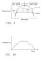
- FIG. 8is a graph of the temperature as a function of enthalpy of the coolant inside the evaporator of FIG. 7 , and further depicting the dome-shaped liquid-vapor phase boundary.
- FIG. 9is a block flow diagram of a two-phase constant temperature cooling process of the invention.
- FIG. 10depicts an exemplary wafer temperature-time profile that may be realized using the invention.
- FIGS. 11A and 11Bare contemporary timing diagrams of the wafer temperature and wafer backside gas pressure, respectively, in accordance with a process for stepping the wafer temperature down in advance of a corresponding ESC temperature change.
- FIGS. 12A and 12Bare contemporary timing diagrams of the wafer temperature and wafer backside gas pressure, respectively, in accordance with a process for stepping the wafer temperature down after completion of a corresponding ESC temperature change.
- FIG. 13illustrates a system similar to that of FIG. 7 but having multiple temperature control loops governing respectively multiple temperature zones.
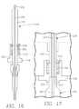
- FIG. 14illustrates an optical temperature sensor of the invention as installed in the ESC of FIG. 7 or FIG. 13 .
- FIG. 15illustrates an upper probe of the temperature sensor of FIG. 14 .
- FIG. 16illustrates a lower probe of the temperature sensor of FIG. 14 .
- FIG. 17is an enlarged view of a portion of FIG. 14 showing how the upper and lower probes are joined together within the ESC.
- FIG. 18is a graph of wafer temperature behavior over time beginning at plasma ignition for three different processes.
- FIG. 19is a diagram of a process of the invention for controlling wafer temperature at and shortly after plasma ignition.
- FIG. 20is a graph of wafer and ESC temperature behaviors over time and a corresponding backside gas pressure profile over time.
- FIG. 21is a diagram of a temperature ramping control process of the invention.
- FIGS. 22A and 22Billustrate wafer temperature behavior over time in different modes of the process of FIG. 21 .
- FIGS. 23A and 23Bare schematic block diagrams of a wafer temperature ramping control system for carrying out the process of FIG. 21 .
- FIG. 24is a simplified schematic block diagram of an ESC thermal model employed in carrying out certain embodiments of the invention.
- FIG. 25is a graph depicting the propagation of a temperature change through the ESC simulated by the thermal model of FIG. 24 .
- FIG. 26depicts a 3-dimensional surface corresponding to a look-up table characterizing one layer of the thermal model of FIG. 24 .
- FIG. 27depicts plural 3-dimensional surfaces corresponding to look-up table characterizing the wafer-puck interface for different backside gas pressures in the thermal model of FIG. 24 .
- FIGS. 28A and 28Bare block diagrams of a feed forward process of the invention for accommodating scheduled RF heat load changes.
- FIG. 29is a graph depicting the propagation of temperature change through the ESC in the process of FIGS. 28A and 28B .
- FIGS. 30A , 30 B and 30 Cdepict wafer temperature behavior in response to ESC temperature changes compensating for an RF heat load change, in cases in which the compensation is late, on time and early, respectively.
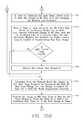
- FIGS. 31A , 31 B and 31 Cconstitute a flow diagram of a feed forward process of the invention for effecting scheduled temperature changes.
- FIGS. 32A and 32Bare contemporaneous time diagrams of wafer temperature, ESC temperature ( FIG. 32A and backside gas pressure ( FIG. 32B ) in a first mode of the feed forward process.
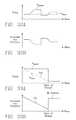
- FIGS. 33A and 33Bare time diagrams of wafer temperature, ESC temperature ( FIG. 33A ) and backside gas pressure ( FIG. 33B ) in a second mode of the feed forward process.
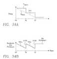
- FIGS. 34A and 34Bare time diagrams of wafer temperature, ESC temperature ( FIG. 34A ) and backside gas pressure ( FIG. 34B ) during operation of a look-ahead loop of the feed forward process of FIGS. 31A-13C .
- FIGS. 35A , 35 B and 35 Cconstitute a flow diagram of a feed forward process corresponding to that of FIGS. 31A-31C , but adapted to compensated for scheduled changes in RF heat load on the wafer.
- FIG. 36is a block diagram of a control system capable of operating both the feed forward process of FIGS. 31A-C and 35 A-C simultaneously.
- a plasma reactorincludes a reactor chamber 100 with a wafer support 105 at the bottom of the chamber supporting a semiconductor wafer 110 .
- a semiconductor ring 115surrounds the wafer 110 .
- the semiconductor ring 115is supported on the grounded chamber body 127 by a dielectric (quartz) ring 120 .
- the chamber 100is bounded at the top by a disc shaped overhead electrode 125 supported at a predetermined gap length above the wafer 110 on grounded chamber body 127 by a dielectric (quartz) seal 130 .
- An RF generator 150applies RF plasma source power to the electrode 125 .
- RF power from the generator 150is coupled through a coaxial cable 162 matched to the generator 150 and into a coaxial stub 135 connected to the electrode 125 .
- the stub 135has a characteristic impedance, resonant frequency determined by its length, and provides an impedance match between the electrode 125 and the 50 Ohm coaxial cable 162 or the 50 Ohm output of the RF power generator 150 .
- the chamber bodyis connected to the RF return (RF ground) of the RF generator 150 .
- the RF path from the overhead electrode 125 to RF groundis affected by the capacitance of the semiconductor ring 115 , the dielectric ring 120 and the dielectric seal 130 .
- the wafer support 105 , the wafer 110 and the semiconductor ring 115provide the primary RF return path for RF power applied to the electrode 125 .
- a large impedance match spaceis realized when the source power frequency, the plasma electrode resonance frequency and the stub resonance frequency are nearly matched.
- three frequenciesare slightly offset from one another, with the source power frequency being 162 MHz (optimized for 300 mm wafers), the electrode-plasma resonant frequency being slightly below 162 MHz, and the stub resonance frequency being slightly above 162 MHz, in order to achieve a de-tuning effect which advantageously reduces the system Q.
- Such a reduction in system Qrenders the reactor performance less susceptible to changes in conditions inside the chamber, so that the entire process is much more stable and can be carried out over a far wider process window.
- the electrode capacitanceis matched to the magnitude of the negative capacitance of the plasma, and the resulting electrode-plasma resonant frequency and the source power frequency are at least nearly matched.
- the matchis possible if the source power frequency is a VHF frequency.
- An advantage of choosing the capacitance of the electrode 125 in this manner, and then matching the resultant electrode-plasma resonant frequency and the source power frequency,is that resonance of the electrode and plasma near the source power frequency provides a wider impedance match and wider process window, and consequently much greater immunity to changes in process conditions, and therefore greater performance stability. Matching the stub resonance frequency to the electrode plasma resonant frequency minimizes reflections at the stub-electrode interface.
- the entire processing systemis rendered less sensitive to variations in operating conditions, e.g., shifts in plasma impedance, and therefore more reliable along with a greater range of process applicability.
- the system Qis reduced to broaden the process window by slightly offsetting the stub resonant frequency, the electrode plasma resonant frequency and the plasma source power frequency from one another.
- the use of the higher VHF source power frequencyproportionately decreases the Q as well. Decreasing system Q broadens the impedance match space of the system, so that its performance is not as susceptible to changes in plasma conditions or deviations from manufacturing tolerances.
- the workpiece support cathode 105includes a metal base layer 05 supporting a lower insulation layer 10 , an electrically conductive mesh layer 15 overlying the lower insulation layer 10 and a thin top insulation layer 20 covering the conductive mesh layer 15 .
- the semiconductor workpiece or wafer 110is placed on top of the top insulation layer 20 .
- RF bias poweris coupled to the conductive mesh layer 15 to control ion bombardment energy at the surface of the wafer 110 .
- the conductive mesh 15also can be used for electrostatically chucking and de-chucking the wafer 110 , and in such a case can be connected to a chucking voltage source in the well-known fashion.
- the conductive mesh 15therefore is not necessarily grounded and can have, alternately, a floating electric potential or a fixed D.C. potential in accordance with conventional chucking and de-chucking operations.
- the metal base layer 05typically (but not necessarily) is connected to ground, and forms part of a return path for VHF power radiated by the overhead electrode 125 .
- An RF bias generator 40produces power in the HF band (e.g., 13.56 MHz). Its RF bias impedance match element 45 is coupled to the conductive mesh 15 by an elongate conductor 25 (hereinafter referred to as an RF conductor) extending through the workpiece support cathode 105 .
- the RF conductor 25is insulated from grounded conductors such as the aluminum base layer 05 .
- the RF conductor 25has a top termination or bias power feed point 25 a in electrical contact with the conductive mesh 15 .
- FIG. 2is a schematic illustration corresponding to FIG. 1 of the circuit consisting of the VHF overhead electrode 125 , the RF bias applied through the workpiece support cathode 105 and the elements of the cathode 105 .
- FIG. 3is a top plan view corresponding to FIG. 1 of the plane of the wafer 110 , with the termination or feed point 25 a of the RF conductor 25 being shown in hidden (dashed) line.
- the RF return path provided by the workpiece support cathode 105consists of two portions in the plane of the wafer 110 , namely a radially inner portion 30 centered about and extending outwardly from the feed point 25 a and a radially outer annular portion 35 .
- the RF return paths provided by the two portions 30 , 35are different, and therefore the two portions 30 , 35 present different impedances to the VHF power radiated by the overhead electrode 125 . Such differences may cause non-uniformities in radial distribution across the wafer surface of impedance to the VHF power, giving rise to nonuniform radial distribution of plasma ion density near the surface of the workpiece.
- a dielectric cylindrical sleeve 50surrounds the RF conductor 25 .
- the axial length and the dielectric constant of the material constituting the sleeve 50determine the feed point impedance presented by the RF conductor 25 to the VHF power.
- the length and dielectric constant of the sleeve 50is selected to bring the feed point impedance to nearly zero at the VHF source power frequency (e.g., 162 MHz).
- the impedance presented by the outer region 35 surrounding the feed point 25 ais nearly a short at 162 MHz (due mainly to the presence of the conductive mesh 15 ).
- the sleeve 50may bring the feed point impedance at the source power frequency to a value closer to that of the surrounding region.
- the impedance of the region surrounding the feed pointis determined mainly by the conductive mesh 15 .
- the sleeve 50can include additional features facilitating the foregoing improvement in VHF power deposition while simultaneously solving a separate problem, namely improving the uniformity in the electric field created by the RF bias power (at 13.56 MHz for example) applied to the wafer 110 by the RF conductor 25 .
- the problemis how to adjust radial distribution of VHF power coupling for maximum uniformity of plasma ion density while simultaneously adjusting the HF bias power electric field distribution across the wafer surface for maximum uniformity.
- FIG. 4is an enlarged view corresponding to FIGS. 1-3 showing how the sleeve 50 can be divided into three sections, namely a top section 52 , a middle section 54 and a bottom section 56 .
- the length and dielectric constant of the sleeve top section 52is selected and fixed to optimize the HF bias power deposition exclusively, and the lengths and dielectric constants of the remaining sleeve sections 54 , 56 are then selected to optimize VHF source power deposition by the overhead electrode while leaving the HF bias power deposition optimized.
- FIG. 5corresponds to an enlarged view of FIG. 1 illustrating the additional feature of an annular RF coupling ring that is placed over and in electrical contact with the outer periphery of the wafer support cathode 105 .
- the top insulation layer 20is surrounded by a removable ring 80 whose top surface 80 a is coplanar with the top surface of the wafer 110 .
- the removable ring 80can be formed of a process-compatible material such as silicon, for example.
- removable metal ground ring 85surrounds the removable ring 80 , its top surface 85 a being coplanar with that of the removable ring 80 .
- a generally planar surfaceis provided across the top of the wafer support cathode 105 bounded by the periphery of the ground ring 85 , facing the generally planar surface of the bottom of the overhead electrode 125 .
- capacitive coupling by the overhead electrode 125is enhanced near the outer portion of the workpiece 110 by placing an RF coupling ring 90 over the removable ring 80 and over grounded ring 85 .
- the RF coupling ring 90may be a conductor, a semiconductor or a dielectric. If the coupling ring 90 is a dielectric, then capacitive coupling to the plasma near the wafer periphery is enhanced by the presence of the dielectric material. If the RF coupling ring 90 is a conductor, it in effect narrows the electrode-to-counterelectrode spacing and thereby enhances capacitance near the peripheral region of the wafer 110 .
- the electrode-to-counterelectrode spacingis h 1 everywhere in the process zone except at the periphery occupied by the RF coupling ring 90 where the spacing is reduced from h 1 by the height h 2 of the coupling ring 90 .
- the increased capacitive coupling of source powerenhances ion density at the periphery.
- the increase in ion densityextends inwardly from the RF coupling ring 90 and extends over a peripheral portion of the workpiece 110 .
- the plasma ion density over the workpiece 110is less center high and may tend toward being more nearly uniform, or possibly slightly edge-high. This condition is optimized by a careful selection of the height (thickness) h 2 of the RF coupling ring 90 .
- FIG. 6illustrates, a modification of the reactor of FIG. 5 in which a second RF coupling ceiling ring 95 is attached to the periphery of the bottom surface of the overhead electrode 125 and overlies the first RF coupling ring 90 . If each ring 90 , 95 has a thickness (height) of h 3 , then the electrode-to-counterelectrode distance near the wafer periphery is reduced by twice h 3 and the capacitance in that region is enhanced proportionately, as in the reactor of FIG. 5 .
- plasma ion density distribution uniformityis improved. Any remaining non-uniformities can be corrected by plasma-steering magnetic fields controlled by a plasma distribution controller 57 (shown in FIG. 1 ) governing D.C. current sources 58 , 59 that drive overhead coils 60 , 65 .
- planar electrode surface 125 aAnother modification that can be employed to enhance plasma processing uniformity across the diameter of the wafer 110 is to change the planar electrode surface 125 a to a convex curved electrode surface 125 b .
- the degree of curvaturecan be selected to compensate for non-uniform plasma ion density radial distribution that may exist with the planar electrode surface 125 a.
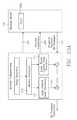
- FIG. 7is an enlarged view of the wafer support pedestal 105 of FIG. 1 , revealing the internal structure of the pedestal 105 .
- the pedestal 105embodies an electrostatic chuck (ESC), as described in FIG. 2 , FIG. 7 showing that the aluminum base 5 contains flow passages 200 for a PCHT medium with an inlet 201 and an outlet 202 .
- the internal flow passages 200constitute the heat exchanger of a PCHT loop, the heat exchanger 200 being internally contained with the ESC base 5 .
- the PCHT loopcan operate in either of two modes, namely a cooling mode (in which the heat exchanger 200 functions as an evaporator) and a heating mode (in which the heat exchanger 200 functions as a condenser).
- the remaining elements of the PCHT loopare external of the ESC 105 , and include (in order of PCHT medium flow direction, starting from the outlet 202 ) an accumulator 204 , a compressor 206 (for pumping the PCHT medium through the loop), and (for the cooling mode of operation) a condenser 208 and an expansion valve 210 having a variable orifice size, all of which are of the type well-known in the art.
- An advantage of locating the heat exchanger 200 inside the ESC base 05is that the delay and losses inherent in the thermal transfer fluid of the prior art are eliminated.
- the PCHT loop(i.e., the heat exchanger 200 , the accumulator 204 , the compressor 206 , the condenser 208 , the expansion valve 210 and the conduits coupling them together, contain the PCHT medium (which functions as a refrigerant or coolant when the PCHT operates in the cooling mode) of a conventional type and can have low electrical conductivity to avoid interfering with the RF characteristics of the reactor.
- the accumulator 204prevents any liquid form of the PCHT medium from reaching the compressor 206 by storing the liquid. This liquid is converted to vapor by appropriately operating the bypass valve 214 .
- the efficiency of the PCHT loopis increased ten-fold or more by operating the PCHT loop 200 , 204 , 206 , 208 , 210 so that the PCHT medium inside the heat exchanger is divided between a liquid phase and a vapor phase.
- the liquid-to-vapor ratio at the inlet 201is sufficiently high to allow for a decrease in this ratio at the outlet 202 . This guarantees that all (or nearly all) heat transfer between the ESC base 05 and the PCHT medium (coolant) within the heat exchanger (evaporator) 200 occurs through contribution to the latent heat of evaporation of the PCHT medium.
- the heat flow in the PCHT loopexceeds, by a factor of 10, the heat flow in a single-phase cooling cycle.
- This conditioncan be satisfied with a decrease in the CPHT medium's liquid-to-vapor ratio from the inlet 201 to the outlet 202 that is sufficiently limited so that at least a very small amount of liquid remains at (or just before) the outlet 202 .
- thisrequires that the coolant capacity of the PCHT loop is not exceeded by the RF heat load on the wafer.
- One way of ensuring thisis to provide the PCHT loop with a maximum cooling capacity that is about twice the maximum anticipated heat load on the wafer. In one implementation of a reactor of the type depicted in FIGS.
- the maximum cooling rate of the PCHT loopwas between about three and four times the maximum anticipated heat load on the wafer.
- the heat load on the waferwas about 30% of the applied RF power on the wafer.
- the liquid-to-vapor ratiowas between about 40% and 60% at the inlet 201 and about 10% at the outlet 202 .
- the PCHT loophas been described with reference primarily to the cooling mode of operation, it can also be employed in a heating mode whenever it is desired to raise the temperature of the ESC (e.g., at a faster rate than plasma heating alone is capable of).
- the condenser 206 and expansion valve 210are bypassed by at least some of the PCHT medium by opening the bypass valve 212 , so as to allow superheated PCHT medium to flow to the heat exchanger 200 .
- the heat exchanger 200functions as a condenser rather than an evaporator.
- the heating modeoverheating of the compressor 206 may be prevented by providing an additional bypass (not shown) from the output of the condenser 206 to the input of the compressor 208 .
- the liquid-to-vapor ratio in the heat exchanger 200may be zero.
- FIG. 8is a phase diagram depicting the enthalpy of the PCHT medium inside the heat exchanger 200 as a function of temperature.
- the temperature-enthalpy boundary between the three phases (liquid, solid, vapor)is a liquid-vapor dome 216 beneath which the PCHT medium exists in both liquid and vapor phases.
- the PCHT mediumis a sub-cooled (100%) liquid phase while to the higher enthalpy side of the dome 216 the PCHT medium is a superheated (100%) vapor.
- the PCHT medium flow rate established by the compressor 206 , the orifice size of the expansion valve 210 and the opening size of a bypass valve 212 that will be discussed later hereinare selected by the skilled worker so that the temperature and enthalpy of the PCHT medium inside the heat exchanger 200 stays under or within the liquid-vapor dome 216 of the phase diagram of FIG. 8 .
- the pressure inside the heat exchanger 200is maintained at a constant level provided that a constant ESC base temperature is desired, so that there is theoretically no temperature change as the coolant flows through the heat exchanger 200 , as indicated by the perfectly horizontal lines of constant pressure 218 a , 218 b of FIG. 8 .
- the PCHT medium's temperature/enthalpy coordinatesfollow a line of constant pressure (e.g., line 218 a ) entering the heat exchanger 200 at a low enthalpy (labeled “inlet” in FIG. 8 ) and exiting at a higher enthalpy (labeled “outlet” in FIG. 8 ), with the entry and exit enthalpies lying inside or on the boundary of the liquid-vapor dome 216 .
- FIG. 8shows that a greater increase in enthalpy (absorbed heat) is achieved at lower coolant temperatures.
- CoolantMaintaining the PCHT medium (hereinafter referred to as “coolant”) inside the evaporator 200 of FIG. 7 within the liquid-vapor dome of FIG. 8 —to guarantee heat extraction through the latent heat of vaporization almost exclusively—solves the problem of non-uniform temperature across the wafer under high RF heat loads. This is because heat transfer via the latent heat of vaporization is a constant-temperature process. In the cooling mode of the PCHT loop, as it absorbs heat, the coolant inside the evaporator 200 does not change temperature. Instead, it changes phase, going from liquid to vapor.
- all the coolant throughout the evaporator 200(the fluid passages inside the ESC base 5 ) is at a uniform temperature regardless of the magnitude of the RF heat load on the wafer.
- the advantageis that the wafer temperature distribution is about as uniform as the electric field distribution across the ESC, so that the etch rate uniformity achieved under the most favorable conditions by the electrical features discussed earlier herein (e.g., the RF bias feedpoint impedance adjustment by multiple dielectric sleeves and the dielectric edge ring process kit) is maintained even under the highest RF heat loads, a result heretofore unattainable.
- This resultrenders the reactor of FIGS. 1-7 useful for plasma processing under the current design rules (small feature sizes) and for several generations of future design rules in which feature sizes may shrink even further, a significant advantage.
- This advantageis combined with the extremely high heat capacity of cooling through latent heat of vaporization (discussed above), which provides about an order of magnitude greater heat flow rate than conventional (sensible) heat transfer via the coolant mass heat capacity.
- the first step in this methodis to enhance or optimize uniformity of radial distribution of the ESC temperature by maintaining the coolant that is inside the evaporator 200 within a range of temperatures and enthalpies at which the heat transfer is through contributions to (or deductions from) the coolant's latent heat of vaporization.
- This stepis depicted in block 300 of FIG. 9 .
- the step of block 300may be carried out by limiting variation in the orifice or opening size of the expansion valve 210 to a range which confines the temperature and enthalpy of the coolant in the evaporator 200 to lie inside the liquid-vapor dome 216 of the temperature-enthalpy diagram of FIG. 8 (block 302 of FIG. 9 ).
- the adjustment range of the expansion valve that confines the coolant inside the liquid-vapor dome 216 of FIG. 8is readily determined and can be pre-programmed into a microprocessor controlling the entire system, for example.
- the step of block 300may also be carried out by adjusting the compressor-to-evaporator bypass flow valve 212 within a range in which the coolant inside the evaporator 200 is maintained inside the liquid-vapor dome 216 of FIG. 8 (block 304 of FIG. 9 ).
- the adjustment of the bypass valve 212 (in the step of block 304 ) and the adjustment of the expansion valve 210 (in the step of block 302 )may be combined to achieve the desired result.
- the next stepis to control the ESC temperature (block 306 of FIG. 9 ). This may be accomplished by adjusting the expansion valve 210 within the range established in the step of block 300 until a desired ESC temperature is reached (block 308 of FIG. 9 ). Alternatively, the ESC temperature may be controlled by adjusting the compressor-to-evaporator bypass valve 212 within the range established in the step of block 304 . This latter step corresponds to block 310 of FIG. 9 . Temperature control may also be carried out by performing the steps of blocks 308 and 310 together.
- variable orifice size of the expansion valve 210is the primary control over cooling rate and wafer temperature
- additional or alternative temperature control and, if desired, heating of the waferis provided by a compressor-to-evaporator bypass valve 212 .
- Complete conversion of all liquid coolant to the gas phase in the accumulator 204can be ensured using a compressor-to-accumulator bypass valve 214 .
- Compressor outlet pressure260-270 PSIG
- Compressor outlet temperature80-100 deg C.
- the inventionmay be implemented with some excursion beyond that limit.
- the coolant's liquid-vapor ratiomay at least nearly reach zero at the evaporator outlet 202 , or may reach zero just before the evaporator outlet 202 , in which case a small amount of sensible heating may occur. In such a case, the vast majority of heat transfer still occurs through the latent heat of vaporization, only a small fraction occurring through sensible heating, so that the advantages of the invention are realized nonetheless.
- the wafer temperaturemay be controlled or held at a desired temperature under a given RF heat load on the wafer 110 using a temperature feedback control loop governing either (or both) the expansion valve 210 and the bypass valve 212 , although the simplest implementation controls the expansion valve 210 only.
- the actual temperatureis sensed at a temperature probe, which may be a temperature probe 220 in the ESC insulating layer 10 , a temperature probe 221 in the ESC base 05 , a temperature probe 222 at the ESC evaporator inlet 201 or a temperature probe 223 at the ESC evaporator outlet 202 or a combination of any or all of these probes.
- a feedback control loop processor 224governs the orifice opening size of the expansion valve 210 in response to input or inputs from one or more of the temperature probes.
- the processor 224is furnished with a user-selected desired temperature value, which may be stored in a memory or user interface 225 .
- the processor 224compares the current temperature measured by at least one of the probes (e.g., by the probe 220 in the ESC insulating layer) against the desired temperature value.
- the processor 224then computes an error value as the difference between the desired and measured temperature values, and determines from the error a correction to the orifice size of either the bypass valve 212 or the expansion valve 210 , that is likely to reduce the error.
- the processor 224then causes the valve orifice size to change in accordance with the correction. This cycle is repeated during the entire duration of a wafer process to control the wafer temperature.
- the waferis cooled to avoid overheating from absorbed RF power by cooling the electrostatic chuck or wafer support pedestal.
- Thermal conductivity between the wafer 110 and the cooled ESC 105is enhanced by injection under pressure of a thermally conductive gas (such as helium) into the interface between the backside of the wafer 110 and the top surface of the ESC 105 , a technique well-known in the art.
- a thermally conductive gassuch as helium
- gas channels 226are formed in the top surface of the ESC insulating layer 20 and a pressurized helium supply 228 is coupled to the internal ESC gas channels 226 through a backside gas pressure valve 229 .
- the wafer 110is electrostatically clamped down onto the top surface of the insulating layer 20 by a D.C. clamping voltage applied by a clamp voltage source 128 to the grid electrode 15 .
- the thermal conductivity between the wafer 110 and the ESC top layer 20is determined by the clamping voltage and by the thermally conductive gas (helium) pressure on the wafer backside.
- Highly agile (quick) wafer temperature controlis carried out in accordance with the present invention by varying the backside gas pressure (by controlling the valve 229 ) so as to adjust the wafer temperature to the desired level.
- the thermal conductivity between the wafer and the ESC top layer 20is changed, which changes the balance between (a) the heat absorbed by the wafer 110 from RF power applied to the grid electrode 15 or coupled to the plasma and (b) the heat drawn from the wafer to the cooled ESC. Changing this balance necessarily changes the wafer temperature.
- a feedback control loop governing the backside gas pressurecan therefore be employed for agile or highly responsive control of the wafer temperature. The response of the wafer temperature to changes in the backside gas pressure is extremely quick (temperature changes reaching equilibrium within a second or less).
- a temperature regulation systememploying the backside gas pressure provides agile temperature control capable of making fast adjustments to wafer temperature.
- FIG. 7illustrates such an agile temperature feedback control system, in which a feedback control loop processor 230 governs the backside gas pressure valve 229 .
- a feedback control loop processor 230governs the backside gas pressure valve 229 .
- One (or more) of the temperature sensors 220 , 221 , 222 or 223 in the ESCmay be connected to an input of the processor 230 .
- a user interface or memory 231may provide a user-selected or desired temperature to the processor 230 .
- the processor 230computes an error signal as the difference between the current temperature measurement (from one of the sensors 220 , 221 , 222 ) and the desired temperature.
- the processor 230determines from that difference a correction to the current setting of the backside gas pressure valve that would tend to reduce the temperature error, and changes the valve opening in accordance with that correction.
- a wafer temperature that is deviating above the desired temperaturewould require increasing the backside gas pressure to increase thermal conductivity to the cooled ESC and bring down the wafer temperature.
- the converseis true in the case of a wafer temperature deviating below the desired temperature.
- the wafer temperaturecan thus be controlled and set to new temperatures virtually instantly within a temperature range whose lower limit corresponds to the chilled temperature of the ESC and whose upper limit is determined by the RF heat load on the wafer.
- the wafer temperaturecannot be increased in the absence of an RF heat load and the wafer temperature cannot be cooled below the temperature of the ESC. If this temperature range is sufficient, then any conventional technique may be used to maintain the ESC at a desired chilled temperature to facilitate the agile temperature feedback control loop governing the backside gas pressure.
- the agile temperature feedback control loop governing the backside gas pressure valve 229 and the large range temperature feedback control loop governing the refrigeration expansion valve 210may be operated simultaneously in a cooperative combination under the control of a master processor 232 controlling both feedback control loop processors 224 , 230 .
- the large range temperature feedback control loop(involving the PCHT loop consisting of the evaporator 200 , the compressor 206 , the condenser 208 and the expansion valve 210 ) controls the workpiece temperature by changing the temperature of the electrostatic chuck 105 .
- the temperature rangeis limited only by the thermal capacity of the PCHT loop and can therefore set the workpiece temperature to any temperature within a very large range (e.g., ⁇ 10 deg C. to +150 deg C.).
- the rate at which it can effect a desired change in workpiece temperature at a particular momentis limited by the thermal mass of the electrostatic chuck 105 . This rate is so slow that, for example, with an electrostatic chuck for supporting a 300 mm workpiece or silicon wafer, a 10 degree C. change in workpiece temperature can require on the order of a minute or more from the time the refrigeration unit begins to change the thermal conditions of the coolant to meet the new temperature until the workpiece temperature finally reaches the new temperature.
- the agile temperature feedback control loopdoes not change the electrostatic chuck temperature (at least not directly) but merely changes the thermal conductivity between the workpiece and the electrostatic chuck.
- the rate at which the workpiece temperature responds to such a changeis extremely high because it is limited only by the rate at which the backside gas pressure can be changed and the thermal mass of the workpiece.
- the backside gas pressureresponds to movement of the valve 229 in a small fraction of a second in a typical system.
- the thermal massis so low that the wafer (workpiece) temperature responds to changes in the backside gas pressure within a matter of a few seconds or a fraction of a second.
- the workpiece temperature response of agile feedback loopis comparatively instantaneous.
- the range over which the agile feedback loop can change the workpiece temperatureis quite limited: the highest workpiece temperature that can be attained is limited by the RF heat load on the wafer, while the lowest temperature cannot be below the current temperature of the electrostatic chuck 105 .
- the advantages of each onecompensate for the limitations of the other, because their combination provides a large workpiece temperature range and a very fast response.
- the master processor 232may be programmed to effect large temperature changes using the large range feedback control loop (the processor 224 ) and effect quick but smaller temperature changes using the agile feedback control loop (the processor 230 ).
- FIG. 10is a graph of one example of wafer temperature behavior over time.
- the solid linedepicts the long term temperature behavior, in which the master processor 232 effects slow large changes in wafer temperature using the large range feedback control loop with the processor 224 .
- the dashed linedepicts fast perturbations in temperature, in which the master processor 232 effects fast but small changes in wafer temperature using the agile feedback control loop with the processor 230 .
- the dual loop control afforded by the master processor 232can be employed to (nearly) instantly move the wafer temperature to a new desired level and hold it there while the ESC temperature slowly changes to the new desired temperature.
- FIGS. 11A and 11BThis is illustrated in FIGS. 11A and 11B .
- the solid line in FIG. 11Adepicts the wafer temperature behavior over time in which the wafer temperature is stepped down to a lower temperature at time t 1 and held there, at which time the PCHT loop (dashed line) begins to cool down the ESC to the lower temperature, which is not reached by the ESC until time t 2 .
- the fast change in wafer temperature at time t 1 and its temperature stability thereafteris accomplished by the agile control loop 230 .
- the agile control loop processor 230receives the new (lower) desired wafer temperature at time t 1 and responds by immediately increasing the backside gas pressure ( FIG. 11B ) to step the wafer temperature down to the new temperature at time t 1 .
- the ESC temperaturebegins to fall in order to drive the ESC to (or slightly below) the new temperature at time t 1 , so that processor 224 increases the refrigeration cooling rate of the ESC to drive its temperature down.
- FIGS. 12A and 12Billustrates how the ESC temperature change may be delayed while the PCHT loop is allowed to slowly adjust to a new temperature (to accommodate a time lag to the ESC surface of about 50 degrees over 5 seconds).
- FIG. 12Adepicts temperature behavior over time while FIG. 12B depicts the corresponding backside gas pressure profile over time.
- the dual loop control afforded by the master processor 232can be employed to temporarily hold the wafer temperature constant (solid line of FIG. 12A ) at an initial temperature level while, beginning at time t 1 , the PCHT loop takes the ESC through a large but slow temperature excursion (dashed line of FIG. 12A ).
- the wafer temperatureis allowed to step down to the new ESC temperature. This is accomplished by cooling the ESC while constantly decreasing the backside gas pressure beginning at time t 1 . Then, after the desired ESC temperature is reached at time t 2 , the agile temperature control loop steps up the backside gas pressure to step the wafer temperature down to the ESC temperature.
- the ESC 105may be divided into plural radial zones, and different independent feedback control loops may separately control the temperature in each zone.
- An advantage of this featureis that different radial zones of the wafer 110 may be kept at different temperatures during processing so as to further reduce process or etch rate distribution non-uniformities.
- the ESC 105is divided into two temperature control zones, namely a radially inner zone 234 and a radially outer zone 236 , and a separate temperature control apparatus is provided for each zone 234 , 236 .
- the radially inner zone 234 of the aluminum base 05contains inner zone coolant flow passages 200 a with a coolant inlet 201 a and a coolant outlet 202 a .
- the inner zone coolant flow passages 200 aconstitute the inner zone evaporator of an inner zone PCHT loop, the evaporator 200 a being internally contained with the inner zone 234 of the ESC base 05 .
- the remaining elements of the inner zone PCHT loopare external of the ESC 105 , and include (in order of coolant flow direction, starting from the coolant outlet 202 a ) an accumulator 204 a , a compressor 206 a , a condenser 208 a and an expansion valve 210 a having a variable orifice size, all of which are of the type well-known in the art.
- the radially outer zone 236 of the aluminum base 05contains outer zone coolant flow passages 200 b with a coolant inlet 201 b and a coolant outlet 202 b .
- the outer zone coolant flow passages 200 bconstitute the outer zone evaporator of an outer zone PCHT loop, the evaporator 200 b being internally contained with the outer zone 236 of the ESC base 05 .
- the remaining elements of the outer zone PCHT loopare external of the ESC 105 , and include (in order of coolant flow direction, starting from the coolant outlet 202 b ) an accumulator 204 b , a compressor 206 b , a condenser 208 b and an expansion valve 210 b having a variable orifice size, all of which are of the type well-known in the art.
- Temperature in the inner zone 234is sensed at one or more of the following inner zone temperature probes: probe 220 a in the inner zone 234 of the ESC insulating layer 10 , probe 221 a in the inner zone of the ESC base 05 , probe 222 a at the inner zone evaporator inlet 201 a or probe 223 a at the inner zone evaporator outlet 202 a.
- An inner zone feedback control loop processor 224 agoverns the orifice opening size of the inner zone expansion valve 210 a in response to input or inputs from one or more of the inner zone temperature probes.
- the inner zone processor 224 ais furnished with a user-selected desired inner zone temperature value, which may be stored in a memory or user interface 225 a .
- the inner zone processor 224 acompares the current temperature measured by at least one of the probes (e.g., the probe 220 a in the ESC insulating layer) against the desired temperature value and corrects the orifice size of the inner zone expansion valve 210 a accordingly.
- An outer zone feedback control loop processor 224 bgoverns the orifice opening size of the outer zone expansion valve 210 b in response to input or inputs from one or more of the outer zone temperature probes.
- the outer zone processor 224 bis furnished with a user-selected desired outer zone temperature value, which may be stored in a memory or user interface 225 b .
- the outer zone processor 224 bcompares the current temperature measured by at least one of the probes (e.g., the outer zone probe 220 b in the ESC insulating layer) against the desired temperature value and corrects the orifice size of the outer zone expansion valve 210 b accordingly.
- thermal conductivity between the wafer 110 and the cooled ESC 105is enhanced by injection under pressure of a thermally conductive gas (such as helium) into the interface between the backside of the wafer 110 and the top surface of the ESC 105 , a technique well-known in the art.
- a thermally conductive gassuch as helium
- inner zone gas channels 226 aare formed in inner zone 234 of the top surface of the ESC insulating layer 20 and a pressurized helium supply 228 a is coupled to the inner zone gas channels 226 a through an inner zone backside gas pressure valve 229 a .
- the wafer 110is electrostatically clamped down onto the top surface of the insulating layer 20 by a D.C.
- the thermal conductivity between the wafer 110 and the ESC top layer 20is determined by the clamping voltage and by the thermally conductive gas (helium) pressure on the wafer backside.
- Highly agile (quick) wafer temperature controlis carried out in the inner temperature zone 234 by controlling the inner zone valve 229 a so as to adjust the wafer temperature to the desired level.
- An inner zone agile feedback control loop processor 230 agoverns the inner zone backside gas pressure valve 229 a .
- One (or more) of the inner zone temperature sensors 220 a , 221 a , 222 a or 223 a in the ESC inner zone 234may be connected to an input of the inner zone agile processor 230 a .
- An inner zone user interface or memory 231 amay provide a user-selected or desired temperature to the inner zone agile processor 230 a .
- the processor 230 asenses an error as the difference between the current temperature measurement (from one of the inner zone sensors 220 a , 221 a , 222 a ) and the desired temperature, and changes the opening of the inner zone backside gas valve 229 a accordingly.
- outer zone gas channels 226 bare formed in outer zone 236 of the top surface of the ESC insulating layer 20 and the pressurized helium supply 228 b is coupled to the outer zone gas channels 226 b through an outer zone backside gas pressure valve 229 b .
- Highly agile (quick) wafer temperature controlis carried out in the outer temperature zone 236 by controlling the outer zone valve 229 b so as to adjust the wafer temperature to the desired level.
- An outer zone agile feedback control loop processor 230 bgoverns the outer zone backside gas pressure valve 229 b .
- One (or more) of the outer zone temperature sensors 220 b , 221 b , 222 b or 223 b in the ESC outer zone 236may be connected to an input of the outer zone agile processor 230 b .
- An outer zone user interface or memory 231 bmay provide a user-selected or desired temperature to the inner zone agile processor 230 b .
- the processor 230 bsenses an error as the difference between the current temperature measurement (from one of the outer zone sensors 220 b , 221 b , 222 b ) and the desired temperature, and changes the opening of the outer zone backside gas valve 229 b accordingly.
- the radial profile of the wafer temperaturemay be controlled over a large range with agile response.
- FIG. 14depicts a preferred temperature probe 238 installed in the plasma reactor of FIG. 1 .
- the probe 238consists of two separable portions, namely an upper probe 239 installed in the ESC 105 and a lower probe 240 installed in a portion of the reactor chamber beneath and supporting the ESC 105 , namely a chamber host base 241 .
- the upper probe 239is depicted in the enlarged view of FIG. 15 , and lies in an area of high RF electric potential (i.e., inside the ESC insulating layer or puck 10 , 20 ).
- the upper probe 239is firmly inserted in an elongate axial hole within the ESC 105 that closely fits the upper probe 239 , and the tip of the upper probe 239 lies very close (e.g., within 3 to 3.5 mm) to the top surface of the puck 20 .
- the advantageis that the probe 239 is sufficiently close to the wafer 110 to minimize or eliminate temperature measurement errors.
- This area of the ESChas very high electric field potential during processing so that any electrical properties that the upper probe 239 may have would have profound effects on plasma processing on the wafer.
- the upper probe 239therefore includes RF compatibility features which minimize or eliminate any effect that the probe 239 might otherwise have on the electric field or on the RF impedance distribution.
- Such RF compatibility featuresensure that the probe 239 does not distort or perturb the ESC electric field or RF impedance distribution that has been so carefully adjusted with the features of the feedpoint impedance adjustment of FIGS. 2-4 and/or the dielectric ring process kit of FIGS. 5-6 (for example).
- the RF compatibility features of the upper probe 239include a complete absence of any conductive materials within the probe 239 , an orientation of the probe in the axial direction (to minimize its effect on the radial electric field or RF impedance distribution) and its small diameter, which is on the order of a fraction of a Debye length of the plasma in the chamber.
- an electrically nonconductive optical temperature transducer 242e.g., a phosphor material whose blackbody radiation spectrum is a well-known function of its temperature.
- the optical temperature transducer 242is coupled to a long thin optical fiber 243 contained within the thin axial upper probe 239 .
- the upper probe 239further includes an opaque cylindrical dielectric sleeve 244 surrounding the optical fiber 243 and preferably consisting of glass-impregnated plastic.
- the optical temperature transducer 242is capped by a dielectric cap 245 of a material that is, preferably, identical to the dielectric material of the ESC puck 10 , 20 , which in the preferred embodiment is aluminum nitride.
- This latter featureensures that the temperature behavior of the material contacting the optical temperature transducer 242 (i.e., the cap 245 ) is identical to the material whose temperature is to be measured (i.e., the ESC puck layer 20 that is in direct contact with the wafer 110 ).
- the upper probe 239further includes a mounting plate 246 that is removably fastened to the bottom surface of the ESC base 05 .
- the mounting plate 246supports a spring housing 247 containing a coil spring 248 compressed between a shoulder 245 of the housing 247 and an annular ring 249 fastened to a portion of the probe sleeve 244 lying within the housing 247 .
- the coil spring 248is compressed to force the tip of the probe 239 to self-align to the top end of the hole.
- the lower probe 240is shown in the enlarged view of FIG. 16 and includes an optical fiber 250 surrounded by an opaque lower cylindrical sleeve 251 . Since the lower probe 240 is below the grounded conductive ESC base 05 , it is located outside of areas of high RF electric fields, and therefore need not be formed of non-conductive materials. In fact, the lower cylindrical sleeve 251 may be formed of steel, for example. The top end 252 of the lower probe 240 is tightly received within a hole 253 in the mounting plate 246 of the upper probe 239 .
- the lower probe 240further includes a mounting plate 254 that is removably fastened to the bottom surface of the chamber housing host base 241 .
- the mounting plate 254supports a spring housing 255 containing a coil spring 256 compressed between a shoulder 257 of the housing 255 and an annular ring 258 fastened to a portion of the lower probe sleeve 251 lying within the housing 255 .
- the coil spring 256is compressed to force the tip of the lower probe 240 to self-align to the top end of the hole 253 .
- the resulting self-alignment of the lower probe 240 against the upper probe 239is illustrated in FIG.
- FIG. 14depicts a single temperature probe whose tip lies near the top of the ESC 105
- another identical probemay be placed in a lower portion of the ESC but at the same radial location as first probe.
- Other identical probesmay be placed at different radial (azimuthal) locations within the ESC but in the same height (axial location) as other probes.
- the temperature probes 220 a , 220 b of the different temperature zones 234 , 236 of FIG. 13may each be of the type described above in FIGS. 13-16 and are located at different radial locations at a common axial height.
- any or all such processorsmay be implemented in a single common processor programmed to perform the functions of each of the individual feedback control loop processors.
- other resources associated with the different control loopssuch as the dual helium supplies 228 a , 228 b , may be implemented with a single supply or resource with separately controlled interfaces (e.g., such as a single helium supply and dual pressure control valves 229 a , 229 b ).
- a common RF bias power sourcemay be employed to apply different levels of RF bias power to the inner and outer mesh electrodes 15 a , 15 b .
- separate RF bias power generatorsmay be employed to realize the separate RF bias power levels.
- the large range temperature control loopcontrols workpiece temperature by regulating the temperature of the electrostatic chuck 105 . It therefore has a slow response attributable to the thermal mass of the electrostatic chuck.
- Another problem with a conventional electrostatic chuck cooling systemis that its efficiency is too limited to avoid upward temperature drift after the wafer temperature has reached the desired level. This leads to workpiece temperature drift during initial processing, which is most pronounced when processing the “first” wafer after the reactor has been idle. This problem is illustrated by the curve labeled 260 in the graph of FIG. 18 depicting a typical wafer temperature response over time when plasma power is turned on at time t 0 .
- the thermal mass of the cooled electrostatic chuck 105slows down the reaction of the wafer temperature to the RF heat load on the wafer. This delays the wafer temperature from reaching the desired temperature from time t 0 until time tb. This delay is typically on the order of tens of seconds or a minute or more.
- the conventional electrostatic chuck cooling apparatushas such limited heat transfer efficiency that it cannot compensate for the accumulation of heat from the RF heat load on the wafer, so that the wafer temperature continues to increase or drift above the desired temperature after time tb. Such uncontrolled changes in temperature degrade control of the plasma process.
- the problem of the temperature drift after time tb(corresponding to the curve 260 of FIG. 18 ) is solved by the superior efficiency of the two-phase refrigeration loop of FIG. 7 .
- the two phase refrigeration loopachieves improved response by locating its evaporator 200 inside the electrostatic chuck 105 . Its efficiency is further improved by an order of magnitude by carrying out heat transfer in the evaporator 200 primarily through latent heat of vaporization. This improved efficiency enables the refrigeration loop to stop the wafer temperature from increasing after the desired temperature has been reached.
- This improved wafer temperature behavioris depicted by the curve of 262 of FIG. 18 , in which the wafer temperature levels off after reaching the desired temperature at time t 2 , and has little or no drift thereafter. This solution nevertheless leaves a significant delay (from time t 0 to time t 2 ) in the wafer temperature reaching the desired level.
- the problem of the delay in bringing the wafer temperature to the desired temperatureis solved by employing the agile feedback control loop processor 230 .
- the valve 229is servoed so as to reduce (or turn off) the backside gas pressure in order to decrease wafer-to-chuck conductance and thus reduce the cooling effect and thermal mass of the electrostatic chuck 105 on the wafer 110 .
- the wafer 110to be quickly heated by the RF heat load with little or no opposition from the cooled chuck 105 , producing a steep rise in temperature beginning at time t 0 , as indicated by the curve labeled 264 of FIG. 18 .
- the wafer temperaturereaches the desired temperature at time ta, the time delay from time t 0 to time ta being extremely short, e.g., on the order of only several seconds or a fraction of a second.
- a preferred embodiment of the present inventionincludes a thermal model of the electrostatic chuck 105 that simulates heat transfer through the various layers of the electrostatic chuck between under given conditions. This feature predicts the optimum backside gas pressure to attain and hold the desired wafer temperature in view of the prevailing conditions.
- FIG. 19depicts one cycle of a control process employing a thermal model. An example of the thermal model which will be described subsequently in this specification.
- the master processor 232can be programmed to interactively repeat the cycle of FIG. 19 to carry out the control process.
- the cyclebegins with inputting the current process conditions into the thermal model (block 270 ). These conditions may include the RF heat load on the wafer (which may be expressed as a predetermined fraction of the total applied RF power), the electrostatic chuck temperature at or near the evaporator 200 , the electrostatic chuck wafer clamping D.C. voltage, and the backside gas pressure.
- the next step (block 271 )is to obtain from the thermal model a prediction of the final or steady state temperature Tf of the wafer produced under the current process condition (i.e., the temperature reached at time tb of FIG. 18 ).
- the thermal modelmay generate a function T(z,t) defining the evolution over time t of the distribution of the temperature T along the axial direction z through the electrostatic chuck 105 .
- Tfis not the desired temperature
- the initial conditionsmay be modified and the foregoing steps repeated until the thermal model yields a satisfactory prediction of Tf.
- the thermal modelis used to find a backside gas pressure (i.e., a setting of the valve 229 ) that would immediately advance the wafer temperature to the predicted steady state temperature Tf (block 272 of FIG. 19 ).
- the backside gas pressureis then set to the optimum value thus identified (block 273 ). If steady state has been reached (block 274 ), the process is stopped. Otherwise, the time index is incremented (block 275 ) and the process cycles back to the step of block 272 .
- FIG. 20is a graph depicting the temperature behavior over time of the wafer 110 (curve labeled 276 ), the top surface or puck layer 20 of the electrostatic chuck 105 (curve labeled 277 ), the bottom or base 5 of the electrostatic chuck 105 (curve labeled 278 ).
- the curve labeled 279depicts the behavior over the same time scale of the backside gas pressure required to achieve the wafer temperature step behavior of curve 276 .
- the curve labeled 280depicts the problematic temperature behavior of the wafer in the absence of any change in backside gas pressure, in which the wafer temperature initially reaches the desired process temperature very slowly during a significant portion of the wafer process. Curve 279 of FIG.
- FIG. 21illustrates how backside gas pressure ramping (by the agile control loop processor 230 ) may control wafer temperature during the entire wafer process. It can do this to maintain the wafer temperature at a constant desired temperature or, alternatively, to accurately follow a rapidly changing wafer temperature profile that may be specified in the user's process recipe.
- the first stepis to define a desired wafer temperature profile of the desired time evolution of the wafer temperature (block 282 of FIG. 21 ).
- the desired temperature for the current timeis determined from the profile (block 283 a ) and input to the thermal model (block 283 b ).
- the current process conditionsare also input to the thermal model (block 284 ), such as wafer backside gas pressure, current wafer temperature, RF heat load on the wafer, ESC base temperature and electrostatic wafer clamping force, for example.
- the thermal modelis then used (block 285 a ) to obtain a correction to the wafer backside gas pressure that would move the current wafer temperature to the current desired temperature value obtained from the user-defined profile. This correction is then made to the wafer backside gas pressure (block 285 b ).
- the value of the current timeis incremented to the next sample time or processor cycle time, and the process cycles back (block 287 ) to the step of block 283 a.
- the backside gas pressurecan be used with the thermal model in the manner depicted in FIG. 21 to control wafer temperature, it is limited to a narrow temperature range defined by a low temperature that is no lower than the ESC evaporator temperature and a high temperature that is limited by the RF heat load on the wafer. Therefore, if the user-specified temperature profile requires changes exceeding this range, then the large range (refrigeration) temperature control loop is be used in conjunction with the agile control loop processor 230 .
- the thermal modelis used (block 286 a ) to obtain a correction to the ESC evaporator (or base) temperature that would move the current wafer temperature to the current desired temperature value obtained from the user-defined profile. This correction is then made to the refrigeration loop, e.g., by adjusting the expansion valve 210 (block 286 b ).
- the respective advantages of the two control loopsare automatically selected for maximum effect depending upon the temperature change to be made.
- the next desired temperature changeis a very large temperature change that is beyond the capability of the agile control loop, then the effect of the large range temperature control loop will dominate.
- the next desired temperature rangeis a very quick temperature change that is too fast for the large range temperature control loop 229 , 230 , then the large temperature control loop cannot even respond, while the agile temperature control loop 229 , 230 effects the needed temperature change.
- FIG. 22Aillustrates an example of a temperature-time profile required by a process recipe. It includes a number slow very large rise in temperature from temperature T 1 to temperature T 2 that is punctuated by a series of sharp steps between Ta and Tb. At the peak (T 3 ), the temperature change is along an arc having a negative rate of change followed by another arc (around temperature T 4 ) having a positive rate of change.
- the temperature scale of FIG. 22Ais such that the agile control processor 230 , using backside gas pressure as in steps 285 a , 285 b of FIG.
- the large range control processor 224is incapable of making the change from T 1 to T 2 , and therefore this large change is made by the large range control processor 224 in steps 286 a , 286 h .
- the time scale of FIG. 21is such that the large range control processor 224 is incapable of effecting the sharp steps between Ta and Tb.
- the small deviation represented by these sharp stepsis made by the agile control processor 230 in the steps of 285 a , 285 b , whose small changes are superimposed upon the long-term temperature rise from T 1 to T 2 made by the large range control processor 224 .
- the sharp arc paths of the temperature profile around T 3 and T 4cannot be emulated by the slow moving large range temperature control loop.
- the agile temperature control loop processor 230provides the fine response (in steps 285 a , 285 b of FIG. 21 ) required to emulate such arcuate paths in the temperature profile.
- the time resolution of the agile temperature control processor 230corresponding to the time period of a single process cycle, can create a staircase effect in tracing the arcuate paths of the desired temperature profile of FIG. 22A if these changes occur over a small time period, as indicated in the corresponding portions of FIG. 22B having a staircase appearance.
- small fine changes or corrections effected by the agile control processor 230 in carrying out the steps of blocks 285 a , 285 b of FIG. 21are superimposed upon the long term large temperature changes made by the large range temperature control processor 224 in carrying out the steps of blocks 286 a , 286 b of FIG. 21 .
- FIGS. 23A and 23Bdepict a modification of the apparatus of FIG. 7 capable of performing the process of FIG. 21 .
- a thermal model 288 of the type referred to aboveis accessible to the apparatus of FIG. 7 , and specifically is accessed by any one or all of the following processors: the master control processor 232 , the large range feedback control loop processor 224 and the agile feedback control loop processor 230 . If both the agile and large range control loop processors 230 , 224 are to access the thermal model 288 , then the agile and large range control loop processors 230 , 224 preferably access the thermal model 288 through the master processor 232 so that the master processor 232 can perform any arbitration that may be necessary.
- Inputs corresponding to the current process conditionsare received at an input 289 of the thermal model. Based upon these inputs, the thermal model 288 generates a time-evolving spatial temperature distribution, T(z,t) that may be exploited to predict steady state temperatures or searched for temperature control settings that could result in achieving a desired temperature, for example.
- the processor 230If the processor 230 is performing the process of FIG. 19 , then it makes a request at a model input 261 for the model 288 to obtain, from T(z,t), the steady state wafer temperature that is reached some time after plasma ignition, and this steady state temperature is defined as the target temperature. On the other hand, if the processor 230 is performing the process of FIG. 21 , then the desired temperature for the current time according to the user profile (e.g., of FIG. 22 ) is applied to the model input 261 . In either case, the processor 230 obtains from an output 263 of the thermal model 288 a correction to the backside gas pressure that will move the wafer temperature closer to the desired temperature. A corresponding command to the pressure valve 229 is transmitted at an output 265 of the processor 230 .
- FIG. 24is a simplified schematic block diagram of one possible embodiment of the thermal model 288 .
- the modelis divided into layers corresponding to the thermal path between the wafer 110 and the evaporator 200 .
- Layer 290represents the heat load on the wafer and is specified as a heat flow rate. This heat flow rate is a function of the RF power applied to the reactor and can be readily determined by the skilled worker.
- Subsequent layersare represented as thermal resistances and heat capacitances.
- the thermal resistanceis a function of the dimensions of the layer and its thermal resistivity or conductivity.
- the heat capacitanceis a function of the layer's specific heat, density and dimensions.
- Layer 291represents the wafer 110 as a thermal resistance 291 a and a thermal capacitance 291 b .
- Layer 292represents the interface between the wafer 110 and the top surface of the ESC puck 20 as a variable thermal resistance 292 a (that change with the backside gas pressure) and a heat capacitance 292 b .
- Layer 293represents the ESC puck 10 , 20 as a puck thermal resistance 293 a and heat capacitance 293 b .
- Layer 294represents the bond or interface between the puck 10 and the ESC base 5 as a thermal resistance 294 a and a heat capacitance 294 b .
- Layer 295represents the ESC base 5 as a base thermal resistance 295 a and a base heat capacitance 295 b .
- the model 288can represent the cooling action of the internal evaporator 200 as a heat sink 296 which is specified by a heat flow rate.
- This heat flow ratemay be determined from the setting of the expansion valve 210 based upon a look-up table that has been previously constructed by the skilled worker from measurement data.
- the thermal model 288must be furnished with the essential initial conditions in order to simulate heat flow through the ESC 105 .
- input 289 of the model 288receives the following inputs, which, in one example, may be supplied by the control processor 230 : the backside gas pressure (from the setting of the valve 229 ), the initial temperature of the ESC base 5 , the initial temperature of the wafer 110 or puck 20 , the power of the heat source 290 representing the wafer RF heat load, and (optionally) the cooling rate (power) of the heat sink 296 .
- the thermal model 288can then be queried (e.g., by the processor 230 ) for specific information, such as the temperature at the wafer 110 as a function of time to determine or predict a steady state temperature after plasma ignition (for example). This corresponds to the step of block 271 of FIG. 19 .
- the thermal model 288may be searched for the best backside gas pressure (or setting of the valve 229 ) that ramps the wafer temperature to a desired value. This latter feature corresponds to the step of block 272 of FIG. 19 and/or to the step of block 286 of FIG. 21 .
- the model 288may produce a spatial distribution T(Z) of the temperature along the Z-axis (i.e., along the stack if layers 291 through 295 ) for each discrete processor sample time, t, within a selected time window.
- This collection of spatial temperature distributionscorresponds to a time-dependent spatial temperature distribution T(Z,t).
- Its time evolutionis depicted qualitatively in FIG. 25 , showing the progress over time of a high temperature zone located at the wafer upon plasma ignition and propagating steadily over time toward the ESC base 5 .
- the thermal modelcan produce different temperature distributions T(Z,t) for different hypothetical backside gas pressure values. Using such robust information, either the thermal model 288 or the control processor 230 can search different distributions T(Z,t) obtained for different backside gas pressure settings for the ideal backside gas pressure setting that provides the desired steady state temperature at the wafer (or other specified location).
- the model of FIG. 24has been described with reference to a lumped element technique employing heat transfer equations in which the thermal characteristics of each layer is inferred from the layer's dimensions and thermal properties.
- the thermal responsemay be characterized from a set of look-up tables empirically constructed from prior measurement data that define the layer's response (e.g., the temperature difference across the layer) as a function of both time and heat flow rate.
- a look-up tablerepresents a three dimensional surface depicted in FIG. 26 lying in a space defined by three orthogonal axes corresponding to heat flow rate, time and temperature difference across the layer.
- Each layermay be thus characterized by one (or more) look-up tables or surfaces of the type depicted in FIG. 26 .
- layers whose thermal response can be varied by a user-controllable external parametersuch as the wafer-ESC interface layer 292 whose thermal resistance is controlled by the backside gas pressure
- a user-controllable external parametersuch as the wafer-ESC interface layer 292 whose thermal resistance is controlled by the backside gas pressure
- each possible setting of the external parametergenerates a different look-up table or surface of the type illustrated in FIG. 26 .
- two surfaces or look-up tablesrepresent the temperature behavior for two of many possible settings of the backside gas pressure by the valve 229 .
- Many such look-up tableswould represent the thermal behavior for a range of backside pressure values. The skilled worker can readily generate such look-up tables for a particular reactor design from measurement data.
- the thermal model 288 of FIG. 24may be used with the multiple temperature zone reactor of FIG. 13 having multiple temperature zones in independent backside gas pressure control is maintained and independent coolant evaporators are provide with independent sets of temperature sensors in each zone, as described above in this specification. If the thermal model 288 of FIG. 24 is combined with the multi-zone reactor of FIG. 13 , then the model 288 can consist of plural thermal models 288 - 1 , 288 - 2 , etc., that simulate the different thermal behavior of the respective plural temperature zones of the electrostatic chuck 105 . Each respective model is employed by the agile and large range feedback temperature control processors of each temperature zone in the manner described above for the single temperature zone reactor of FIG. 7 . Thus, the processes of FIGS. 19 and 21 are carried out for each temperature zone of FIG. 13 individually and independently, the process in each zone using the corresponding one of the thermal models 288 - 1 , 288 - 2 , etc.
- Some plasma process recipesmay require changing the RF heat load on the wafer to achieve different process effects at different steps in the process, without changing the wafer temperature.
- the problemis that the thermal mass of the electrostatic chuck imposes a large (e.g., 1 to 2 minute) delay between a change in the cooling system's temperature or cooling rate and the consequent effect on wafer temperature.
- the large range temperature control loop(using the evaporator 200 ) has such a slow response that it cannot compensate for sudden changes in the RF heat load on the wafer without permitting a significant drift in wafer temperature before regaining stability.
- agile temperature control through the backside gas pressure valve 229might not be able to compensate for large changes in RF heat load on the wafer.
- the agile temperature controle.g., the agile temperature control loop
- the backside gas pressure valve 229controlling only the backside gas pressure valve 229 (“agile temperature control”) may not be sufficient to compensate for a sudden large increase in RF heat load.
- agile temperature controlmay not be sufficient to compensate for a sudden large decrease in RF heat load.
- thermal model 288analyzing (in the thermal model 288 ) the magnitude and time of the next scheduled change in RF head load.
- the thermal model 288yields a correction in ESC base temperature which is most likely to compensate for the RF heat load change and maintain constant wafer temperature.
- the thermal modelpredicts the amount of time it takes for this temperature correction to propagate through the ESC 105 and reach the wafer 110 .
- the temperature controller 228implements the recommended change in ESC base temperature sufficiently early (based upon the predicted propagation time) so that the temperature shift in the ESC base reaches the wafer at the time of the scheduled change in RF power level/RF heat load.
- FIGS. 28A and 28BThis feed forward feature is illustrated in FIGS. 28A and 28B (hereinafter referred to collectively as FIG. 28 ) and can be carried out, for the most part, by the large range control loop and its processor 230 .
- the thermal model 288is furnished with the current process conditions, such as the RF power (RF wafer heat load), wafer temperature, ESC base temperature, backside gas pressure, and the like (block 300 of FIG. 28 ). If the current plasma processing recipe calls for a change in RF power level to be made at some later time, then the magnitude and time of this RF power change is input to the thermal model 288 (block 301 of FIG. 28 ). The thermal model 288 then simulates the effects on wafer temperature of this planned change in RF power.
- the current process conditionssuch as the RF power (RF wafer heat load), wafer temperature, ESC base temperature, backside gas pressure, and the like.
- the thermal model 288is searched for a change in ESC base temperature that would precisely compensate for the planned change in RF power level. This is accomplished by changing (at the input 289 to the thermal model 288 ) the ESC base temperature and observing the changing effect on the wafer temperature behavior simulated by the model 288 .
- the ESC base temperature change that best compensates for the change in RF heat loadis selected (block 302 of FIG. 28 ).
- the thermal model 288can compute or indicate the transit time required for the temperature change at the ESC base 5 to reach the wafer 110 (block 303 of FIG. 28 ).
- the compensating change in ESC base temperatureis then made in advance of the time of the planned change in RF power by a lead time equal to the base-to-wafer transit time of the compensating base temperature change (block 304 of FIG. 28 ). (This advance in timing may be included in the simulation of the step of block 302 .)
- the agile temperature control loop 229 , 230maintains a constant wafer temperature (block 305 of FIG. 28 ).
- the compensating base temperature changecauses a premature drop in ESC puck temperature prior to the planned change in RF power level
- the backside gas pressurewould be automatically decreased by the agile temperature control processor 230 to decrease heat conductance from the wafer and thereby hold the wafer temperature constant during this period.
- This correction cyclecan include simultaneously monitoring plural temperature sensors periodically placed in axial alignment along the Z-axis inside the ESC 105 , such as the temperature sensors 220 , 221 of FIG. 7 (although more than two axially aligned periodically spaced sensors may be employed in this step).
- an instantaneous temperature profile T(Z)may be deduced (block 306 of FIG. 28B ).
- This instantaneous temperature distributionis input to the thermal model 288 (block 307 of FIG. 28B ).
- the thermal model 288uses the instantaneous temperature distribution of the step of block 307 as the updated “initial” condition to generate a new updated version of the time-evolving temperature profile T(Z,t). From this, the thermal model 288 can predict the behavior of the wafer temperature around the time (tc) of the scheduled RF power level change (block 309 of FIG. 28A ). Using these results, the predicted wafer temperature (or its average) at time tc is compared (block 310 of FIG.
- FIG. 29is a graph depicting the time evolution of the spatial temperature distribution in which the feed forward feature of FIGS. 28A and 28B responds to a planned step up in applied RF power at a future time tc by reducing the ESC base temperature at time t 0 .
- the step down in temperaturepropagates toward the wafer plane in the direction of the Z axis.
- the maximum temperature depressionreaches the wafer plane at time tc, so that there is no overcorrection or undercorrection in this idealized example.
- the contemporaneous time plots of FIGS. 30A through 30Cdepict the effects of overcorrection and undercorrection.
- FIG. 30A through 30Cdepict the effects of overcorrection and undercorrection.
- FIG. 30Adepicts applied RF power as a function time, in which a step-up in power occurs at time tc.
- FIG. 30Bdepicts wafer temperature behavior over time, in which the corrective step-down in ESC base temperature is undertaken too late or with insufficient temperature change. In either case, the wafer temperature begins to climb above the desired temperature at time tc and begins to return toward the desired level only after making a significant deviation.
- FIG. 30Cdepicts wafer temperature behavior over time, in which, the corrective step-down in ESC base temperature is undertaken too earlier or with an excessive temperature change. In such a case, the wafer temperature begins to fall at time tc, and begins to return toward the desired level only after making a significant deviation. In the ideal case, the wafer temperature remains constant before, during and after the RF power step-up at time tc.
- Some plasma process recipesmay require changing the wafer temperature during plasma processing to achieve different process effects at different steps in the process. With such changes, the process recipe may (or may not) leave the RF heat load on the wafer unchanged.
- the problemis that the thermal mass of the electrostatic chuck imposes a large (e.g., 1 to 2 minute) delay between a change in the cooling system's temperature or cooling rate and the consequent effect on wafer temperature.
- the large range temperature control loopusing the evaporator 200 ) has such a slow response that it may not be able to make sudden wafer temperature changes required by the process recipe.
- the agile temperature control loop 229 , 230might not be able to make extremely large changes in wafer temperature that may be required by the process recipe. Specifically, if either the ESC base temperature is too high or initial RF heat load is too great, the agile control loop 229 , 230 may not be able to carry out a large decrease in wafer temperature required by the process recipe. Conversely, if either ESC base temperature is too low or the initial RF heat load is insufficient, then the agile control loop 229 , 230 may not be able to carry out a large increase in wafer temperature required by the process recipe.
- thermal model 288analyzing (in the thermal model 288 ) the magnitude and time of the next scheduled change in wafer temperature called for by the process recipe. If the temperature change is beyond the capability of the agile temperature control loop 229 , 230 (the backside gas pressure control), then the large range control loop 224 , 210 (the refrigeration control) is employed to effect the desired temperature change. In this case, the thermal model 288 yields an ESC base temperature change which is most likely to effect the desired wafer temperature change. The thermal model predicts the amount of time it takes for this temperature correction to propagate through the ESC 105 and reach the wafer 110 .
- the temperature controller 224implements the recommended change in ESC base temperature sufficiently early (based upon the predicted propagation time) so that the temperature shift in the ESC base reaches the wafer at the time of the scheduled change in wafer temperature. Just before this, the agile temperature control loop 229 , 230 (using backside gas pressure)) maintains the wafer temperature constant until the scheduled time of wafer temperature change.
- the agile temperature control 229 , 230(backside gas pressure) is capable by itself of making the desired wafer temperature change, then the agile control loop 229 , 230 is called upon to perform the change at the scheduled time, in which case the large range control loop 224 , 210 can leave the ESC temperature constant or change it in preparation for a later wafer temperature change.
- FIG. 31This feed forward feature is illustrated in the block flow diagram of FIGS. 31A , 31 B and 31 C (hereinafter referred to collectively as FIG. 31 ) and can be carried out by the master processor 232 of FIG. 7 using the thermal model of FIGS. 24-26 .
- a time value t 0is set to the process start time (block 320 of FIG. 31 ).
- the process recipeis inspected to find the next scheduled change in wafer temperature and its scheduled time, t 1 (block 322 of FIG. 31 ).
- This changeis made (by servoing the expansion valve 210 ) beginning at time sufficient for the desired temperature change to propagate through the ESC 105 and reach the wafer by the scheduled time t 1 (block 328 ). Meanwhile, until time t 1 , the agile temperature control loop 229 , 230 is commanded to maintain the wafer temperature at the initial temperature (block 330 ). To do this, the agile temperature control processor 230 servoes the backside gas pressure valve 229 (to change the thermal conductance through the wafer-ESC interface) so as to compensate for changes in the ESC temperature.
- the agile control loop processor 230is commanded to allow the wafer temperature to follow the change in ESC temperature so as to effect the desired wafer temperature change (block 332 ).
- the present timeis advanced beyond time t 1 (block 334 ) and the process cycles back to the step of block 322 .
- step of block 324if the agile temperature control loop 229 , 230 is found to be capable of making the desired wafer temperature change (YES branch of block 324 a or 324 b ), then the process proceeds to the step of block 336 , in which the agile temperature control processor 230 is commanded to wait until time t 1 and then make the desired wafer temperature change (by servoing the backside gas pressure valve 229 ). However, prior to time t 1 , a look-ahead step (block 338 ) is performed whose main purpose is to ensure timely preparation of the ESC temperature for a very large scheduled swing in wafer temperature, in order to allow for thermal propagation delay through the ESC 105 .
- This stepminimizes (or eliminates) the possibility that a scheduled large swing in wafer temperature requiring a corresponding change in ESC temperature is not addressed in time to allow for thermal propagation delay from the ESC evaporator 200 to the wafer 110 .
- the process recipeis scanned beyond time t 1 to find the next change in wafer temperature and its scheduled time of occurrence t 2 .
- a determinationis made whether the agile temperature control loop 22 , 230 is capable of making this next change.
- This determinationcan entail determining whether the RF heat load on the wafer is sufficiently high if the change is a temperature increase (block 338 a ), or determining whether the ESC temperature is sufficiently low if the change is a temperature decrease (block 338 b ). If it is determined that the agile temperature control loop 229 , 230 is capable of making the desired wafer temperature change (YES branch of block 338 a or 338 b ), then the change is effected by servoing the backside gas pressure valve 229 to effect the desired temperature change (block 339 ). The present time is advanced beyond t 1 (block 340 ) and the process cycles back to the step of block 322 .
- the thermal model 288is used to determine a change in ESC base temperature that will produce the desired change in wafer temperature (block 342 ) and this change is performed by servoing the expansion valve 210 either at the present time or at a later time which is, nevertheless, sufficiently early to allow for the thermal propagation delay through the ESC 105 (block 344 ) to effect the needed change by the scheduled time t 2 .
- the agile temperature control processor 230is commanded to regulate the wafer temperature (block 346 of FIG. 31C ) as follows: From the present time until time t 1 , the backside gas pressure is varied as necessary to hold the wafer temperature constant against any changes in ESC temperature (block 346 a ). At time t 1 , the backside gas pressure is stepped to make the wafer temperature changed scheduled in the process recipe for time t 1 (block 346 b ). From time t 1 and until time t 2 , the backside gas pressure is varied to compensate for changes in ESC temperature and hold the wafer temperature constant at the new temperature (block 346 c ).
- the agile temperature control processor 230stops its efforts to hold the wafer temperature constant and allows (by increasing the backside gas pressure to increase thermal conductance) the new ESC temperature to drive the wafer temperature in accordance with change scheduled for time t 2 (block 346 d ). Then, the present time is advanced past time t 2 (block 348 ) and the process cycles back to the step of block 322 . The process continues in this manner until completion of the process recipe.
- the step of block 324determines whether the agile temperature control loop 229 , 230 (using backside gas pressure changes) alone is capable of making the desired wafer temperature change, as discussed above. If the answer is always “yes” (at least over a number of successive temperature changes), then the ESC base temperature can be relegated to a constant role and the only changes made are successive changes in the backside gas pressure valve 229 . This corresponds to the case of the process of FIG. 31 taking the YES branch of blocks 324 a or 324 b over successive iterations. The result is illustrated in FIGS. 32A and 32B in which the ESC base temperature remains at a constant level indicated by the dashed line of FIG.
- FIG. 32A(e.g., by leaving the expansion valve 210 of FIG. 7 at a constant setting) while the backside gas pressure ( FIG. 32B ) is servoed to follow successive changes in the wafer temperature specified by the process recipe.
- the corresponding wafer temperature behavior(solid line of FIG. 32A ) appears as an inverse of the backside gas pressure behavior ( FIG. 32B ), in the general case in which the ESC acts as a heat sink for the RF heat load on the wafer. (There is a special but rare case in which the required wafer temperature is so high—or the RF heat load is so low—that the ESC 105 is, employed as a heat source.)
- 32A and 32Btherefore correspond to a simple mode of the invention in which the ESC base temperature is held at a constant level while the wafer backside gas pressure is varied as required by the process recipe.
- This modemay be implemented with any cooling device coupled to the ESC 105 , such as the constant temperature refrigeration loop of FIG. 7 of the present invention or (alternatively) a conventional prior art refrigeration apparatus.
- FIGS. 33A and 33Billustrate base and wafer temperature behavior and backside gas pressure profile for the case in which the step of 324 finds that the agile control loop 229 , 230 is not capable of making the required change in wafer temperature.
- the large range control loop 228 , 210 , 200 , etc.begins to change the ESC base temperature prior to the scheduled time of change in the step of block 328 .
- This causes the ESC base temperature to changei.e., drop, in the case of an up-coming temperature change that is a decrease in wafer temperature), as illustrated in dashed line in FIG. 33A .
- the agile control loop 229 , 230holds the wafer temperature constant until the scheduled time of change (solid line of FIG. 33A ). This is done by offsetting the ESC base temperature change with a corresponding change (decrease) in backside gas pressure, as illustrated in FIG. 33B . At the time of change, the backside gas pressure is stepped up to enable the wafer to follow the latest change in ESC temperature.
- FIGS. 34A and 34Bdepict the operation of the look-ahead loop of blocks 338 - 346 of FIG. 31 .
- the step of block 338discovers that, even though the agile temperature control loop can make the next wafer temperature change (scheduled for time t 1 ), it is incapable of making the subsequent change scheduled for time t 2 . Therefore, the decision is made to use the large range temperature control loop 224 , 210 , 200 , etc. of FIG. 7 to effect the desired wafer temperature change.
- the required change in ESC base temperaturemust begin immediately in order for its full effect to reach the wafer by time t 2 .
- the required change in position of the expansion valve 210is made at time t 0 , so that the ESC temperature begins to change (e.g., decrease, in this example), as indicated by the dashed line of FIG. 34A .
- FIG. 34Ashows that the ESC temperature (as measured near the wafer) reaches the required level just before time t 2 , and therefore is held at that new temperature thereafter.
- the backside gas pressureFIG. 34B
- the backside gas pressuredecreases in order to hold the wafer temperature constant, in accordance with the step 346 a of FIG. 31 .
- the backside gas pressureis stepped to a different level to achieve the wafer temperature change scheduled for time t 1 , in accordance with the step of block 346 b of FIG. 31 .
- the wafer temperatureis held at this new level by varying the backside gas pressure to offset the effect at the wafer of the changing ESC temperature, in accordance with the step of block 346 c of FIG. 31 .
- the backside gas pressureis restored to a high thermal conductance level to permit the new ESC temperature to bring about the change in wafer temperature scheduled for time t 2 .
- the feed forward process of FIG. 31is described as carrying out scheduled changes in wafer temperature, it may be modified to counteract scheduled changes in RF heat load on the wafer. Such a process is illustrated in FIGS. 35A , 35 B and 35 C, which will now be described.
- the first step, block 420defines present time t 0 as process start time.
- the next step, block 422determines from the temperature profile of the process recipe an upcoming change in RF heat load on the wafer its scheduled time of occurrence (time t 1 ).
- the following determinationsmay be made: whether the change is an increase in RF heat load, is the present ESC base temperature sufficiently low (block 424 a ); whether the change is a decrease in RF heat load, is the present RF heat load sufficiently high or will the changed RF heat load be sufficiently high (block 424 b ).
- the next stepis to determine from the thermal model 288 the change in ESC base temperature required to counteract the change in RF heat load and keep the wafer temperature constant.
- This change in ESC base temperatureis then performed (by controlling the refrigeration loop expansion valve 210 ) in time for the temperature change to reach the wafer by or before time t 1 , the scheduled time of occurrence (block 428 ).
- the agile temperature control loop 229 , 230is used to hold the wafer at its present temperature against changes in ESC temperature (block 430 ).
- the agile temperature control loop processor 230allows the changed ESC temperature to counteract the RF heat load change (block 432 ).
- the time index (present time)is then advanced beyond time t 1 (block 434 ) and the process loops back to the step of block 422 .
- step of block 424determines that the agile control loop 229 , 230 is capable of meeting the change in RF heat load (YES branch of blocks 438 a or 438 b ), then later, at time t 1 , the agile temperature control loop 229 , 230 changes the backside gas pressure to meet the change in RF heat load (block 436 ). Meanwhile, prior to time t 1 , the process looks ahead (in the RF power time profile of the process recipe) to the next (e.g., second) scheduled change in RF heat load and its scheduled time of occurrence (time t 2 ) and determines whether the agile control loop 229 , 230 is capable of counteracting this next RF heat load change (block 438 ).
- the large range temperature control loop controlling ESC temperaturemust be used instead. Therefore, in the next step, the thermal model 288 is used to determine the change in ESC base temperature required to counteract the next RF heat load change (i.e., the change scheduled for time t 2 ) to hold the wafer temperature constant (block 442 ). This change in ESC base temperature is then performed by the large range control loop 224 , 210 , 200 in time for the temperature change to reach the wafer by or before the scheduled time (time t 2 ) of next change in wafer temperature (block 444 ).
- the agile temperature control loop 229 , 230regulates the wafer temperature against the changing ESC temperature (block 446 ). It does this as follows: hold the wafer temperature constant until time t 1 (i.e., mask changes in ESC temperature with changes in backside gas pressure) (block 446 a ); at time t 1 , compensate for the RF heat load change scheduled for time t 1 (i.e., step the backside gas pressure to a new level) (block 446 b ); hold the wafer temperature constant after time t 1 and until time t 2 (i.e., mask changes in ESC temperature with changes in backside gas pressure) (block 446 c ); at time t 2 , allow the change in ESC temperature to counteract the RF heat load change scheduled for time t 2 (i.e., increase the wafer-ESC thermal conductance by increasing the backside gas pressure) (block 446 d ). Thereafter, the present time index is advanced beyond time t 2 (block 448 ) and the process loops
- a complex wafer temperature time profilemay have to be implemented while accommodating scheduled swings in RF heat load on the wafer.
- Thiscan be achieved by operating the RF heat load feed forward loop of FIGS. 28A-B and the temperature profile feed forward loop of FIG. 31 together, using the master processor to arbitrate or superimpose different control commands from the two feed forward loops addressed to the large range control loop processor 224 (governing the expansion valve 210 of FIG. 7 ) as well as different control commands from the two feed forward loops addressed to the agile control loop processor 230 (governing the backside gas pressure valve 229 of FIG. 7 ).
- FIG. 36Such a combination is depicted in FIG. 36 discussed below.
- the two feed forward processesare implemented simultaneously based upon temperature measurements from the reactor forwarded through the master processor 232 .
- the RF heat load feed forward process 350(corresponding to FIG. 28 ) is furnished with the schedule 351 of changes in RF power or heat load specified by the process recipe.
- the temperature profile feed forward process 352(corresponding to FIG. 31 ) is furnished with the schedule 353 of wafer temperature changes specified by the process recipe.
- the master processor 232combines these simultaneous commands and forwards them to the expansion valve 210 and the backside gas pressure valve 229 through the large range control processor 224 and the agile control processor 230 respectively.
Landscapes
- Engineering & Computer Science (AREA)
- Physics & Mathematics (AREA)
- Microelectronics & Electronic Packaging (AREA)
- General Physics & Mathematics (AREA)
- Manufacturing & Machinery (AREA)
- Computer Hardware Design (AREA)
- Condensed Matter Physics & Semiconductors (AREA)
- Power Engineering (AREA)
- Plasma & Fusion (AREA)
- Chemical & Material Sciences (AREA)
- Analytical Chemistry (AREA)
- Drying Of Semiconductors (AREA)
- Container, Conveyance, Adherence, Positioning, Of Wafer (AREA)
- Physical Vapour Deposition (AREA)
Abstract
Description
Claims (19)
Priority Applications (1)
| Application Number | Priority Date | Filing Date | Title |
|---|---|---|---|
| US12/855,670US8980044B2 (en) | 2005-10-20 | 2010-08-12 | Plasma reactor with a multiple zone thermal control feed forward control apparatus |
Applications Claiming Priority (3)
| Application Number | Priority Date | Filing Date | Title |
|---|---|---|---|
| US72931405P | 2005-10-20 | 2005-10-20 | |
| US11/408,559US8012304B2 (en) | 2005-10-20 | 2006-04-21 | Plasma reactor with a multiple zone thermal control feed forward control apparatus |
| US12/855,670US8980044B2 (en) | 2005-10-20 | 2010-08-12 | Plasma reactor with a multiple zone thermal control feed forward control apparatus |
Related Parent Applications (1)
| Application Number | Title | Priority Date | Filing Date |
|---|---|---|---|
| US11/408,559ContinuationUS8012304B2 (en) | 2005-10-20 | 2006-04-21 | Plasma reactor with a multiple zone thermal control feed forward control apparatus |
Publications (2)
| Publication Number | Publication Date |
|---|---|
| US20100314046A1 US20100314046A1 (en) | 2010-12-16 |
| US8980044B2true US8980044B2 (en) | 2015-03-17 |
Family
ID=38063386
Family Applications (10)
| Application Number | Title | Priority Date | Filing Date |
|---|---|---|---|
| US11/409,184AbandonedUS20070091540A1 (en) | 2005-10-20 | 2006-04-21 | Method of processing a workpiece in a plasma reactor using multiple zone feed forward thermal control |
| US11/408,567Active2028-12-12US8221580B2 (en) | 2005-10-20 | 2006-04-21 | Plasma reactor with wafer backside thermal loop, two-phase internal pedestal thermal loop and a control processor governing both loops |
| US11/408,558Active2028-09-16US8021521B2 (en) | 2005-10-20 | 2006-04-21 | Method for agile workpiece temperature control in a plasma reactor using a thermal model |
| US11/409,183Active2027-01-16US8608900B2 (en) | 2005-10-20 | 2006-04-21 | Plasma reactor with feed forward thermal control system using a thermal model for accommodating RF power changes or wafer temperature changes |
| US11/409,326AbandonedUS20070091541A1 (en) | 2005-10-20 | 2006-04-21 | Method of processing a workpiece in a plasma reactor using feed forward thermal control |
| US11/408,559Active2027-03-24US8012304B2 (en) | 2005-10-20 | 2006-04-21 | Plasma reactor with a multiple zone thermal control feed forward control apparatus |
| US12/855,670Active2029-09-06US8980044B2 (en) | 2005-10-20 | 2010-08-12 | Plasma reactor with a multiple zone thermal control feed forward control apparatus |
| US12/855,674ActiveUS8092639B2 (en) | 2005-10-20 | 2010-08-12 | Plasma reactor with feed forward thermal control system using a thermal model for accommodating RF power changes or wafer temperature changes |
| US12/949,028Active2026-05-16US8329586B2 (en) | 2005-10-20 | 2010-11-18 | Method of processing a workpiece in a plasma reactor using feed forward thermal control |
| US12/953,793Active2027-04-05US8546267B2 (en) | 2005-10-20 | 2010-11-24 | Method of processing a workpiece in a plasma reactor using multiple zone feed forward thermal control |
Family Applications Before (6)
| Application Number | Title | Priority Date | Filing Date |
|---|---|---|---|
| US11/409,184AbandonedUS20070091540A1 (en) | 2005-10-20 | 2006-04-21 | Method of processing a workpiece in a plasma reactor using multiple zone feed forward thermal control |
| US11/408,567Active2028-12-12US8221580B2 (en) | 2005-10-20 | 2006-04-21 | Plasma reactor with wafer backside thermal loop, two-phase internal pedestal thermal loop and a control processor governing both loops |
| US11/408,558Active2028-09-16US8021521B2 (en) | 2005-10-20 | 2006-04-21 | Method for agile workpiece temperature control in a plasma reactor using a thermal model |
| US11/409,183Active2027-01-16US8608900B2 (en) | 2005-10-20 | 2006-04-21 | Plasma reactor with feed forward thermal control system using a thermal model for accommodating RF power changes or wafer temperature changes |
| US11/409,326AbandonedUS20070091541A1 (en) | 2005-10-20 | 2006-04-21 | Method of processing a workpiece in a plasma reactor using feed forward thermal control |
| US11/408,559Active2027-03-24US8012304B2 (en) | 2005-10-20 | 2006-04-21 | Plasma reactor with a multiple zone thermal control feed forward control apparatus |
Family Applications After (3)
| Application Number | Title | Priority Date | Filing Date |
|---|---|---|---|
| US12/855,674ActiveUS8092639B2 (en) | 2005-10-20 | 2010-08-12 | Plasma reactor with feed forward thermal control system using a thermal model for accommodating RF power changes or wafer temperature changes |
| US12/949,028Active2026-05-16US8329586B2 (en) | 2005-10-20 | 2010-11-18 | Method of processing a workpiece in a plasma reactor using feed forward thermal control |
| US12/953,793Active2027-04-05US8546267B2 (en) | 2005-10-20 | 2010-11-24 | Method of processing a workpiece in a plasma reactor using multiple zone feed forward thermal control |
Country Status (5)
| Country | Link |
|---|---|
| US (10) | US20070091540A1 (en) |
| JP (2) | JP4540644B2 (en) |
| KR (2) | KR100830059B1 (en) |
| CN (4) | CN101699613B (en) |
| TW (5) | TWI380364B (en) |
Cited By (7)
| Publication number | Priority date | Publication date | Assignee | Title |
|---|---|---|---|---|
| US20160240366A1 (en)* | 2015-02-17 | 2016-08-18 | Infineon Technologies Ag | Processing of Semiconductor Devices |
| US20160307738A1 (en)* | 2013-10-01 | 2016-10-20 | Lam Research Corporation | Control of impedance of rf delivery path |
| US20170069465A1 (en)* | 2014-05-19 | 2017-03-09 | Trumpf Huettinger Gmbh + Co. Kg | Control Arrangement, Control System and High Frequency Power Generating Device |
| US20170085060A1 (en)* | 2008-01-31 | 2017-03-23 | West Virginia University | Quarter wave coaxial cavity igniter for combustion engines |
| US10249476B2 (en) | 2013-10-01 | 2019-04-02 | Lam Research Corporation | Control of impedance of RF return path |
| US11437261B2 (en) | 2018-12-11 | 2022-09-06 | Applied Materials, Inc. | Cryogenic electrostatic chuck |
| US12100609B2 (en) | 2019-04-15 | 2024-09-24 | Applied Materials, Inc. | Electrostatic chucking process |
Families Citing this family (137)
| Publication number | Priority date | Publication date | Assignee | Title |
|---|---|---|---|---|
| DE10216786C5 (en)* | 2002-04-15 | 2009-10-15 | Ers Electronic Gmbh | Method and apparatus for conditioning semiconductor wafers and / or hybrids |
| US7789962B2 (en)* | 2005-03-31 | 2010-09-07 | Tokyo Electron Limited | Device and method for controlling temperature of a mounting table, a program therefor, and a processing apparatus including same |
| US7718225B2 (en)* | 2005-08-17 | 2010-05-18 | Applied Materials, Inc. | Method to control semiconductor film deposition characteristics |
| US8034180B2 (en)* | 2005-10-11 | 2011-10-11 | Applied Materials, Inc. | Method of cooling a wafer support at a uniform temperature in a capacitively coupled plasma reactor |
| US8092638B2 (en) | 2005-10-11 | 2012-01-10 | Applied Materials Inc. | Capacitively coupled plasma reactor having a cooled/heated wafer support with uniform temperature distribution |
| US7988872B2 (en)* | 2005-10-11 | 2011-08-02 | Applied Materials, Inc. | Method of operating a capacitively coupled plasma reactor with dual temperature control loops |
| US8157951B2 (en)* | 2005-10-11 | 2012-04-17 | Applied Materials, Inc. | Capacitively coupled plasma reactor having very agile wafer temperature control |
| US20070091540A1 (en) | 2005-10-20 | 2007-04-26 | Applied Materials, Inc. | Method of processing a workpiece in a plasma reactor using multiple zone feed forward thermal control |
| KR100706790B1 (en)* | 2005-12-01 | 2007-04-12 | 삼성전자주식회사 | Oxidation treatment apparatus and method |
| US8226769B2 (en)* | 2006-04-27 | 2012-07-24 | Applied Materials, Inc. | Substrate support with electrostatic chuck having dual temperature zones |
| US9275887B2 (en) | 2006-07-20 | 2016-03-01 | Applied Materials, Inc. | Substrate processing with rapid temperature gradient control |
| JP4815295B2 (en)* | 2006-07-26 | 2011-11-16 | 株式会社日立ハイテクノロジーズ | Plasma processing equipment |
| US20080121821A1 (en)* | 2006-11-27 | 2008-05-29 | Varian Semiconductor Equipment Associates Inc. | Techniques for low-temperature ion implantation |
| US7528391B2 (en) | 2006-12-22 | 2009-05-05 | Varian Semiconductor Equipment Associates, Inc. | Techniques for reducing contamination during ion implantation |
| JP5203612B2 (en)* | 2007-01-17 | 2013-06-05 | 株式会社日立ハイテクノロジーズ | Plasma processing equipment |
| US20080267257A1 (en)* | 2007-04-27 | 2008-10-30 | Sokudo Co., Ltd. | Method and System for Detecting Substrate Temperature in a Track Lithography Tool |
| JP4898556B2 (en)* | 2007-05-23 | 2012-03-14 | 株式会社日立ハイテクノロジーズ | Plasma processing equipment |
| TWI508129B (en)* | 2007-10-31 | 2015-11-11 | Lam Res Corp | Temperature control module using gas pressure to control thermal conductance between liquid coolant and component body |
| JP2009111301A (en)* | 2007-11-01 | 2009-05-21 | Hitachi High-Technologies Corp | Plasma processing equipment |
| JP5297048B2 (en)* | 2008-01-28 | 2013-09-25 | 三菱重工業株式会社 | Plasma processing method and plasma processing apparatus |
| JP5222442B2 (en)* | 2008-02-06 | 2013-06-26 | 東京エレクトロン株式会社 | Substrate mounting table, substrate processing apparatus, and temperature control method for substrate to be processed |
| US20090274590A1 (en)* | 2008-05-05 | 2009-11-05 | Applied Materials, Inc. | Plasma reactor electrostatic chuck having a coaxial rf feed and multizone ac heater power transmission through the coaxial feed |
| JP5210706B2 (en)* | 2008-05-09 | 2013-06-12 | 株式会社日立ハイテクノロジーズ | Plasma processing apparatus and plasma processing method |
| US8596336B2 (en)* | 2008-06-03 | 2013-12-03 | Applied Materials, Inc. | Substrate support temperature control |
| JP2010016159A (en)* | 2008-07-03 | 2010-01-21 | Hitachi High-Technologies Corp | Plasma processing method and plasma processing apparatus |
| US9155134B2 (en) | 2008-10-17 | 2015-10-06 | Applied Materials, Inc. | Methods and apparatus for rapidly responsive heat control in plasma processing devices |
| JP5185790B2 (en)* | 2008-11-27 | 2013-04-17 | 株式会社日立ハイテクノロジーズ | Plasma processing equipment |
| DE102008064080A1 (en)* | 2008-12-19 | 2010-07-01 | Converteam Gmbh | Method and device for operating a power semiconductor component |
| KR101050463B1 (en)* | 2009-05-07 | 2011-07-20 | 삼성모바일디스플레이주식회사 | Plasma processing equipment |
| JP2010278166A (en)* | 2009-05-27 | 2010-12-09 | Tokyo Electron Ltd | Annular component for plasma treatment, and plasma treatment device |
| KR101108337B1 (en)* | 2009-12-31 | 2012-01-25 | 주식회사 디엠에스 | Temperature control device of electrostatic chuck including two stages of refrigerant passage |
| US9338871B2 (en)* | 2010-01-29 | 2016-05-10 | Applied Materials, Inc. | Feedforward temperature control for plasma processing apparatus |
| US8916793B2 (en) | 2010-06-08 | 2014-12-23 | Applied Materials, Inc. | Temperature control in plasma processing apparatus using pulsed heat transfer fluid flow |
| WO2011118408A1 (en)* | 2010-03-24 | 2011-09-29 | 積水化学工業株式会社 | Plasma treatment device |
| JP5465151B2 (en)* | 2010-04-23 | 2014-04-09 | 住友電装株式会社 | Reactor |
| US8410393B2 (en)* | 2010-05-24 | 2013-04-02 | Lam Research Corporation | Apparatus and method for temperature control of a semiconductor substrate support |
| US8880227B2 (en)* | 2010-05-27 | 2014-11-04 | Applied Materials, Inc. | Component temperature control by coolant flow control and heater duty cycle control |
| US8608852B2 (en)* | 2010-06-11 | 2013-12-17 | Applied Materials, Inc. | Temperature controlled plasma processing chamber component with zone dependent thermal efficiencies |
| JP5606970B2 (en)* | 2011-03-14 | 2014-10-15 | ルネサスエレクトロニクス株式会社 | Manufacturing method of semiconductor device |
| JP5781803B2 (en)* | 2011-03-30 | 2015-09-24 | 東京エレクトロン株式会社 | Temperature control method and plasma processing system |
| JP2012238629A (en)* | 2011-05-10 | 2012-12-06 | Hitachi High-Technologies Corp | Heat treatment apparatus |
| US9245719B2 (en) | 2011-07-20 | 2016-01-26 | Lam Research Corporation | Dual phase cleaning chambers and assemblies comprising the same |
| JP5822578B2 (en)* | 2011-07-20 | 2015-11-24 | 東京エレクトロン株式会社 | Mounting table temperature control apparatus and substrate processing apparatus |
| JP5750339B2 (en)* | 2011-08-31 | 2015-07-22 | 株式会社ニューフレアテクノロジー | Vapor phase growth method and vapor phase growth apparatus |
| US10274270B2 (en) | 2011-10-27 | 2019-04-30 | Applied Materials, Inc. | Dual zone common catch heat exchanger/chiller |
| CN103094155A (en)* | 2011-11-07 | 2013-05-08 | 无锡华润上华科技有限公司 | Processing equipment of semiconductor device |
| JP5947023B2 (en)* | 2011-11-14 | 2016-07-06 | 東京エレクトロン株式会社 | Temperature control apparatus, plasma processing apparatus, processing apparatus, and temperature control method |
| CN103137517B (en)* | 2011-11-25 | 2016-08-03 | 中芯国际集成电路制造(北京)有限公司 | For processing the reaction unit of wafer, electrostatic chuck and wafer temperature control method |
| CN103327723A (en)* | 2012-03-23 | 2013-09-25 | 中微半导体设备(上海)有限公司 | Capacity coupling plasma reactor and control method thereof |
| KR101932169B1 (en) | 2012-03-23 | 2018-12-27 | 삼성디스플레이 주식회사 | Apparatus and method for treating substrate |
| CN103367216A (en)* | 2012-03-26 | 2013-10-23 | 上海宏力半导体制造有限公司 | Aqueduct and electrostatic chuck therewith |
| US20130309785A1 (en)* | 2012-05-18 | 2013-11-21 | Applied Materials, Inc. | Rotational absorption spectra for semiconductor manufacturing process monitoring and control |
| JP6011417B2 (en)* | 2012-06-15 | 2016-10-19 | 東京エレクトロン株式会社 | Film forming apparatus, substrate processing apparatus, and film forming method |
| US8969177B2 (en)* | 2012-06-29 | 2015-03-03 | Applied Materials, Inc. | Laser and plasma etch wafer dicing with a double sided UV-curable adhesive film |
| KR102025540B1 (en)* | 2012-08-28 | 2019-09-26 | 에이이에스 글로벌 홀딩스 피티이 리미티드 | Wide dynamic range ion energy bias control; fast ion energy switching; ion energy control and pulsed bias supply; and a virtual front panel |
| US20140060739A1 (en)* | 2012-08-31 | 2014-03-06 | Rajinder Dhindsa | Rf ground return in plasma processing systems and methods therefor |
| US20140069334A1 (en)* | 2012-09-10 | 2014-03-13 | Semicat, Inc. | Temperature control of semiconductor processing chambers by modulating plasma generation energy |
| CN103794527B (en)* | 2012-10-30 | 2016-08-24 | 中微半导体设备(上海)有限公司 | Electrostatic chuck heating means |
| KR102098981B1 (en)* | 2012-11-27 | 2020-04-08 | 가부시키가이샤 크리에이티브 테크놀러지 | Electrostatic chuck, glass substrate processing method, and said glass substrate |
| CN103022272A (en)* | 2012-12-22 | 2013-04-03 | 蚌埠玻璃工业设计研究院 | Device preparing non-crystalline silicon/non-crystalline germanium-silicon laminated solar cell thin films |
| CN104637838B (en)* | 2013-11-15 | 2018-06-26 | 中微半导体设备(上海)有限公司 | A kind of semiconductor processing device |
| US9716022B2 (en) | 2013-12-17 | 2017-07-25 | Lam Research Corporation | Method of determining thermal stability of a substrate support assembly |
| CN103760753B (en)* | 2013-12-31 | 2017-04-12 | 深圳市华星光电技术有限公司 | Substrate roasting device and temperature adjustment method thereof |
| US20150228514A1 (en)* | 2014-02-12 | 2015-08-13 | Axcelis Technologies, Inc. | Multi Fluid Cooling System for Large Temperature Range Chuck |
| CN105097402A (en)* | 2014-05-23 | 2015-11-25 | 中微半导体设备(上海)有限公司 | Plasma processing chamber and composite component of a DC electrode and a heating device of the plasma processing chamber |
| TWI734668B (en)* | 2014-06-23 | 2021-08-01 | 美商應用材料股份有限公司 | Substrate thermal control in an epi chamber |
| KR101605717B1 (en)* | 2014-07-16 | 2016-03-23 | 세메스 주식회사 | Apparatus and method for treating substrate |
| CN105374657B (en)* | 2014-07-18 | 2017-07-25 | 中微半导体设备(上海)有限公司 | Plasma processing apparatus and its temprature control method |
| KR102411194B1 (en) | 2014-09-04 | 2022-06-20 | 삼성전자주식회사 | Electrostatic chuck assemblies capable of bidirectional flow of coolant and semiconductor fabricating apparatus having the same |
| US9753463B2 (en)* | 2014-09-12 | 2017-09-05 | Applied Materials, Inc. | Increasing the gas efficiency for an electrostatic chuck |
| US9872341B2 (en) | 2014-11-26 | 2018-01-16 | Applied Materials, Inc. | Consolidated filter arrangement for devices in an RF environment |
| US20160149733A1 (en)* | 2014-11-26 | 2016-05-26 | Applied Materials, Inc. | Control architecture for devices in an rf environment |
| US10186444B2 (en)* | 2015-03-20 | 2019-01-22 | Applied Materials, Inc. | Gas flow for condensation reduction with a substrate processing chuck |
| JP6524753B2 (en)* | 2015-03-30 | 2019-06-05 | 東京エレクトロン株式会社 | PLASMA PROCESSING APPARATUS, PLASMA PROCESSING METHOD, AND STORAGE MEDIUM |
| US10386821B2 (en) | 2015-06-22 | 2019-08-20 | Lam Research Corporation | Systems and methods for calibrating scalar field contribution values for a limited number of sensors including a temperature value of an electrostatic chuck and estimating temperature distribution profiles based on calibrated values |
| US10381248B2 (en)* | 2015-06-22 | 2019-08-13 | Lam Research Corporation | Auto-correction of electrostatic chuck temperature non-uniformity |
| US10763142B2 (en) | 2015-06-22 | 2020-09-01 | Lam Research Corporation | System and method for determining field non-uniformities of a wafer processing chamber using a wafer processing parameter |
| JP6655310B2 (en) | 2015-07-09 | 2020-02-26 | 株式会社日立ハイテクノロジーズ | Plasma processing equipment |
| CN105097408B (en)* | 2015-07-21 | 2017-09-26 | 深圳市华星光电技术有限公司 | A kind of dry etching board and its application method |
| JP6570390B2 (en) | 2015-09-24 | 2019-09-04 | 東京エレクトロン株式会社 | Temperature control apparatus and substrate processing apparatus |
| US10515786B2 (en)* | 2015-09-25 | 2019-12-24 | Tokyo Electron Limited | Mounting table and plasma processing apparatus |
| US9847892B2 (en) | 2016-01-22 | 2017-12-19 | International Business Machines Corporation | Embedded wire feed forward equalization |
| US11837479B2 (en) | 2016-05-05 | 2023-12-05 | Applied Materials, Inc. | Advanced temperature control for wafer carrier in plasma processing chamber |
| FR3052856B1 (en)* | 2016-06-21 | 2019-06-14 | Valeo Systemes Thermiques | CIRCULATING LOOP OF A REFRIGERANT FLUID FOR A VEHICLE |
| JP2018537662A (en)* | 2016-09-20 | 2018-12-20 | ルマセンス テクノロジーズ ホールディングズ, インク. | Temperature probe |
| CN108257839B (en)* | 2016-12-29 | 2019-10-08 | 中微半导体设备(上海)股份有限公司 | A kind of reaction chamber for wafer-process |
| US20180235110A1 (en)* | 2017-02-16 | 2018-08-16 | Lam Research Corporation | Cooling system for rf power electronics |
| JP6803815B2 (en)* | 2017-07-25 | 2020-12-23 | 東京エレクトロン株式会社 | Substrate processing equipment and operation method of substrate processing equipment |
| US10636630B2 (en) | 2017-07-27 | 2020-04-28 | Applied Materials, Inc. | Processing chamber and method with thermal control |
| US20190087711A1 (en)* | 2017-09-15 | 2019-03-21 | Battelle Energy Alliance, Llc | Intelligent, adaptive control system and related methods for integrated processing of biomass |
| US10505348B2 (en)* | 2017-09-15 | 2019-12-10 | Mks Instruments, Inc. | Apparatus and method for ignition of a plasma system and for monitoring health of the plasma system |
| US10415899B2 (en)* | 2017-12-28 | 2019-09-17 | Asm Ip Holding B.V. | Cooling system, substrate processing system and flow rate adjusting method for cooling medium |
| US11691119B2 (en)* | 2018-02-09 | 2023-07-04 | China Petroleum & Chemical Corporation | Low temperature plasma reaction device and hydrogen sulfide decomposition method |
| CN110124482A (en)* | 2018-02-09 | 2019-08-16 | 中国石油化工股份有限公司 | The method of reaction of low temperature plasma device and decomposing hydrogen sulfide |
| JP7101024B2 (en)* | 2018-04-03 | 2022-07-14 | 東京エレクトロン株式会社 | Temperature control system |
| JP7101023B2 (en)* | 2018-04-03 | 2022-07-14 | 東京エレクトロン株式会社 | Temperature control method |
| JP7094131B2 (en)* | 2018-04-03 | 2022-07-01 | 東京エレクトロン株式会社 | Cleaning method |
| JP7454504B2 (en)* | 2018-04-12 | 2024-03-22 | ラム リサーチ コーポレーション | Determination and control of substrate temperature during substrate processing |
| WO2019204124A1 (en)* | 2018-04-20 | 2019-10-24 | Applied Materials, Inc. | Ceramic wafer heater with integrated pressurized helium cooling |
| WO2019204125A1 (en)* | 2018-04-21 | 2019-10-24 | Applied Materials, Inc. | Ceramic wafer heater having cooling channels with minimum fluid drag |
| KR102757324B1 (en)* | 2018-05-24 | 2025-01-20 | 어플라이드 머티어리얼스, 인코포레이티드 | Virtual sensors for spatially resolved wafer temperature control |
| US10573532B2 (en) | 2018-06-15 | 2020-02-25 | Mattson Technology, Inc. | Method for processing a workpiece using a multi-cycle thermal treatment process |
| US11456203B2 (en)* | 2018-07-13 | 2022-09-27 | Taiwan Semiconductor Manufacturing Co., Ltd | Wafer release mechanism |
| JP7112915B2 (en)* | 2018-09-07 | 2022-08-04 | 東京エレクトロン株式会社 | temperature control system |
| WO2020117371A1 (en)* | 2018-12-07 | 2020-06-11 | Applied Materials, Inc. | Ground electrode formed in an electrostatic chuck for a plasma processing chamber |
| CN109659266B (en)* | 2018-12-19 | 2020-11-24 | 上海华力微电子有限公司 | Method for improving current stability of etching cavity |
| CN111383885B (en) | 2018-12-27 | 2023-03-31 | 中微半导体设备(上海)股份有限公司 | Substrate mounting table capable of improving temperature control precision and plasma processing equipment |
| CN111383882B (en)* | 2018-12-27 | 2023-03-10 | 中微半导体设备(上海)股份有限公司 | Plasma processing apparatus and substrate holder for the same |
| CN113557597B (en)* | 2019-03-08 | 2025-04-11 | 应用材料公司 | Adsorption process and system for substrate processing chamber |
| TWI886128B (en)* | 2019-05-30 | 2025-06-11 | 美商蘭姆研究公司 | Rf immune sensor probe for monitoring a temperature of an electrostatic chuck of a substrate processing system |
| US12266588B2 (en) | 2019-07-16 | 2025-04-01 | Lam Research Corporation | Thermoelectric cooling pedestal for substrate processing systems |
| WO2021016223A1 (en)* | 2019-07-25 | 2021-01-28 | Lam Research Corporation | In situ real-time sensing and compensation of non-uniformities in substrate processing systems |
| CN110600419A (en)* | 2019-09-20 | 2019-12-20 | 上海华力微电子有限公司 | Electrostatic chuck and using method thereof |
| US11887820B2 (en)* | 2020-01-10 | 2024-01-30 | COMET Technologies USA, Inc. | Sector shunts for plasma-based wafer processing systems |
| US11335543B2 (en)* | 2020-03-25 | 2022-05-17 | Applied Materials, Inc. | RF return path for reduction of parasitic plasma |
| US11615966B2 (en) | 2020-07-19 | 2023-03-28 | Applied Materials, Inc. | Flowable film formation and treatments |
| US11264203B1 (en)* | 2020-08-17 | 2022-03-01 | Applied Materials Israel Ltd. | Reducing a temperature difference between a sample and a chuck of an electron beam tool |
| US11887811B2 (en)* | 2020-09-08 | 2024-01-30 | Applied Materials, Inc. | Semiconductor processing chambers for deposition and etch |
| US11699571B2 (en) | 2020-09-08 | 2023-07-11 | Applied Materials, Inc. | Semiconductor processing chambers for deposition and etch |
| US12142459B2 (en) | 2020-09-08 | 2024-11-12 | Applied Materials, Inc. | Single chamber flowable film formation and treatments |
| CN115989568A (en)* | 2020-09-28 | 2023-04-18 | 株式会社国际电气 | Temperature control method, method for manufacturing semiconductor device, program, and substrate processing apparatus |
| US11694869B2 (en)* | 2020-12-08 | 2023-07-04 | Applied Materials Israel Ltd. | Evaluating a contact between a wafer and an electrostatic chuck |
| CN114688457B (en)* | 2020-12-29 | 2024-05-14 | 中微半导体设备(上海)股份有限公司 | Gas supply system of plasma processing device |
| KR102584512B1 (en)* | 2020-12-31 | 2023-10-05 | 세메스 주식회사 | Buffer unit and method for storaging substrate type senseor for measuring of horizontal of a substrate support member provided on the atmosphere in which temperature changes are accompanied by |
| TWI803809B (en)* | 2021-01-18 | 2023-06-01 | 得立亞科技有限公司 | Parametric Analysis Method for Electrostatic Chuck |
| JP7619732B2 (en)* | 2021-01-22 | 2025-01-22 | 東京エレクトロン株式会社 | Holder temperature detection method, holder monitoring method, and substrate processing apparatus |
| KR20220151982A (en)* | 2021-05-07 | 2022-11-15 | 주성엔지니어링(주) | substrate processing apparatus and processing method using the same |
| US12341048B2 (en)* | 2021-11-29 | 2025-06-24 | Applied Materials, Inc. | Porous plug for electrostatic chuck gas delivery |
| US20230195060A1 (en)* | 2021-12-21 | 2023-06-22 | Applied Materials, Inc. | Substrate support characterization to build a digital twin |
| US12142461B2 (en)* | 2022-05-05 | 2024-11-12 | Applied Materials, Inc. | Control and prediction of multiple plasma coupling surfaces and corresponding power transfer |
| CN118016497A (en)* | 2022-11-09 | 2024-05-10 | 北京北方华创微电子装备有限公司 | Wafer carrying device and semiconductor process equipment |
| TW202509701A (en)* | 2023-04-17 | 2025-03-01 | 日商東京威力科創股份有限公司 | Computer program, information processing device, and information processing method |
| DE102023112894A1 (en)* | 2023-05-16 | 2024-11-21 | Creavac-Creative Vakuumbeschichtung Gmbh | Device for cooling a sputtering target |
| CN117316831B (en)* | 2023-11-28 | 2024-02-02 | 南昌中微半导体设备有限公司 | Pressure controller, semiconductor processing apparatus, and air pressure control method |
| KR102833519B1 (en)* | 2023-12-28 | 2025-07-11 | 세메스 주식회사 | Substrate treating apparatus |
| CN119144934B (en)* | 2023-12-29 | 2025-06-24 | 北京北方华创微电子装备有限公司 | Temperature control method, device, electronic device and storage medium |
| CN120366738A (en)* | 2025-06-11 | 2025-07-25 | 福建金石能源有限公司 | PECVD vacuum coating equipment and cooling method of vacuum coating chamber |
Citations (131)
| Publication number | Priority date | Publication date | Assignee | Title |
|---|---|---|---|---|
| US2707868A (en)* | 1951-06-29 | 1955-05-10 | Goodman William | Refrigerating system, including a mixing valve |
| US3826304A (en) | 1967-10-11 | 1974-07-30 | Universal Oil Prod Co | Advantageous configuration of tubing for internal boiling |
| US3933004A (en) | 1973-04-26 | 1976-01-20 | Shipowners Refrigerated Cargo Research Association | Refrigeration control systems |
| US4042686A (en) | 1975-05-14 | 1977-08-16 | Basf Aktiengesellschaft | Fungicidal compositions |
| US4313783A (en) | 1980-05-19 | 1982-02-02 | Branson International Plasma Corporation | Computer controlled system for processing semiconductor wafers |
| US4384918A (en) | 1980-09-30 | 1983-05-24 | Fujitsu Limited | Method and apparatus for dry etching and electrostatic chucking device used therein |
| US4705951A (en) | 1986-04-17 | 1987-11-10 | Varian Associates, Inc. | Wafer processing system |
| JPS6329220A (en) | 1986-07-23 | 1988-02-06 | Matsushita Electric Ind Co Ltd | light temperature sensor |
| US4752141A (en) | 1985-10-25 | 1988-06-21 | Luxtron Corporation | Fiberoptic sensing of temperature and/or other physical parameters |
| US4798650A (en) | 1987-03-27 | 1989-01-17 | Fujitsu Limited | Method of dry etching aluminum |
| US4835977A (en) | 1983-11-18 | 1989-06-06 | Teledyne Industries, Inc. | Apparatus and method of air-conditioning parked aircraft |
| US4853534A (en) | 1987-03-11 | 1989-08-01 | Plessey Overseas Limited | Optical fiber sensing system |
| US4883354A (en) | 1985-10-25 | 1989-11-28 | Luxtron Corporation | Fiberoptic sensing of temperature and/or other physical parameters |
| US4934155A (en) | 1986-03-18 | 1990-06-19 | Mydax, Inc. | Refrigeration system |
| US5057968A (en) | 1989-10-16 | 1991-10-15 | Lockheed Corporation | Cooling system for electronic modules |
| JPH05144777A (en) | 1991-11-21 | 1993-06-11 | Sony Corp | Low temperature dry etching apparatus |
| JPH05163096A (en) | 1991-12-11 | 1993-06-29 | Applied Materials Japan Kk | Low temperature control system for electrodes of vacuum equipment using refrigerator in semiconductor manufacturing equipment |
| US5258614A (en) | 1991-05-13 | 1993-11-02 | The Babcock & Wilcox Company | Optical fiber loop temperature sensor |
| US5320982A (en) | 1990-07-02 | 1994-06-14 | Hitachi, Ltd. | Wafer cooling method and apparatus |
| JPH06331457A (en) | 1993-05-19 | 1994-12-02 | Hitachi Ltd | Temperature detecting device and semiconductor manufacturing method and device using the temperature detecting device |
| US5410889A (en) | 1994-01-14 | 1995-05-02 | Thermo King Corporation | Methods and apparatus for operating a refrigeration system |
| US5471850A (en) | 1993-07-09 | 1995-12-05 | Acurex Corporation | Refrigeration system and method for very large scale integrated circuits |
| US5549756A (en) | 1994-02-02 | 1996-08-27 | Applied Materials, Inc. | Optical pyrometer for a thin film deposition system |
| US5551249A (en) | 1992-10-05 | 1996-09-03 | Van Steenburgh, Jr.; Leon R. | Liquid chiller with bypass valves |
| US5556204A (en) | 1990-07-02 | 1996-09-17 | Hitachi, Ltd. | Method and apparatus for detecting the temperature of a sample |
| US5567267A (en) | 1992-11-20 | 1996-10-22 | Tokyo Electron Limited | Method of controlling temperature of susceptor |
| US5625526A (en) | 1993-06-01 | 1997-04-29 | Tokyo Electron Limited | Electrostatic chuck |
| US5650082A (en) | 1993-10-29 | 1997-07-22 | Applied Materials, Inc. | Profiled substrate heating |
| US5701758A (en) | 1996-01-30 | 1997-12-30 | Haramoto; Cary | Refrigeration system accumulating vessel having a brazed, metal-clad deflector |
| US5742022A (en) | 1995-04-19 | 1998-04-21 | Dct Avanced Engineering, Inc. | Industrial workcell system and method |
| US5748435A (en) | 1996-12-30 | 1998-05-05 | Applied Materials, Inc. | Apparatus for controlling backside gas pressure beneath a semiconductor wafer |
| US5761023A (en) | 1996-04-25 | 1998-06-02 | Applied Materials, Inc. | Substrate support with pressure zones having reduced contact area and temperature feedback |
| US5762009A (en) | 1995-06-07 | 1998-06-09 | Alliant Techsystems, Inc. | Plasma energy recycle and conversion (PERC) reactor and process |
| US5787723A (en) | 1995-08-21 | 1998-08-04 | Manitowoc Foodservice Group, Inc. | Remote ice making machine |
| US5815396A (en) | 1991-08-12 | 1998-09-29 | Hitachi, Ltd. | Vacuum processing device and film forming device and method using same |
| US5878583A (en) | 1997-04-01 | 1999-03-09 | Manitowoc Foodservice Group, Inc. | Ice making machine and control method therefore |
| US5886866A (en) | 1998-07-06 | 1999-03-23 | Applied Materials, Inc. | Electrostatic chuck having a combination electrode structure for substrate chucking, heating and biasing |
| US5888907A (en) | 1996-04-26 | 1999-03-30 | Tokyo Electron Limited | Plasma processing method |
| US5937660A (en) | 1993-07-26 | 1999-08-17 | Lau; Billy Ying Bui | Quick cooling air conditioning system |
| US5970731A (en) | 1997-11-21 | 1999-10-26 | International Business Machines Corporation | Modular refrigeration system |
| US5994675A (en) | 1997-03-07 | 1999-11-30 | Semitool, Inc. | Semiconductor processing furnace heating control system |
| US6015465A (en) | 1998-04-08 | 2000-01-18 | Applied Materials, Inc. | Temperature control system for semiconductor process chamber |
| US6018616A (en) | 1998-02-23 | 2000-01-25 | Applied Materials, Inc. | Thermal cycling module and process using radiant heat |
| JP2000028213A (en) | 1998-07-14 | 2000-01-28 | Sanyo Electric Co Ltd | Compression refrigeration machine |
| US6033482A (en) | 1998-04-10 | 2000-03-07 | Applied Materials, Inc. | Method for igniting a plasma in a plasma processing chamber |
| US6076366A (en) | 1998-04-03 | 2000-06-20 | Denso Corporation | Refrigerating cycle system with hot-gas bypass passage |
| US6091060A (en) | 1997-12-31 | 2000-07-18 | Temptronic Corporation | Power and control system for a workpiece chuck |
| US6094334A (en) | 1999-03-02 | 2000-07-25 | Applied Materials, Inc. | Polymer chuck with heater and method of manufacture |
| US6098408A (en) | 1998-11-11 | 2000-08-08 | Advanced Micro Devices | System for controlling reflection reticle temperature in microlithography |
| US6125025A (en) | 1998-09-30 | 2000-09-26 | Lam Research Corporation | Electrostatic dechucking method and apparatus for dielectric workpieces in vacuum processors |
| US6135052A (en) | 1995-12-15 | 2000-10-24 | Sony Corporation | Method and apparatus for temperature control of the semiconductor |
| US6169274B1 (en) | 1999-03-01 | 2001-01-02 | Tokyo Electron Ltd. | Heat treatment apparatus and method, detecting temperatures at plural positions each different in depth in holding plate, and estimating temperature of surface of plate corresponding to detected result |
| US6174408B1 (en) | 1996-02-26 | 2001-01-16 | Sony Corporation | Method and apparatus for dry etching |
| US6196553B1 (en) | 1998-07-30 | 2001-03-06 | Litton Systems, Inc. | Fiber optical connector seal |
| US6205803B1 (en) | 1996-04-26 | 2001-03-27 | Mainstream Engineering Corporation | Compact avionics-pod-cooling unit thermal control method and apparatus |
| US6262397B1 (en) | 1999-03-30 | 2001-07-17 | Tokyo Electron Ltd. | Heat treatment apparatus and heat treatment method |
| US6283632B1 (en) | 1992-11-25 | 2001-09-04 | Terumo Cardiovascular Systems Corporation | Method of measuring temperature |
| US6320736B1 (en) | 1999-05-17 | 2001-11-20 | Applied Materials, Inc. | Chuck having pressurized zones of heat transfer gas |
| US6318384B1 (en) | 1999-09-24 | 2001-11-20 | Applied Materials, Inc. | Self cleaning method of forming deep trenches in silicon substrates |
| JP2001358121A (en) | 2000-04-11 | 2001-12-26 | Applied Materials Inc | Correction of wafer temperature drift in plasma reactor based on continuous wafer temperature measurement using in situ wafer temperature optical probe |
| US20020000198A1 (en) | 1997-05-29 | 2002-01-03 | Applied Materials, Inc. | The dome: shape and temperature controlled surfaces |
| US20020014894A1 (en) | 2000-07-19 | 2002-02-07 | Toshihiro Yonezawa | Temperature control apparatus |
| US6397629B2 (en) | 1999-01-12 | 2002-06-04 | Xdx, Llc | Vapor compression system and method |
| US6412344B1 (en) | 1999-11-15 | 2002-07-02 | Rosemount Aerospace Inc. | Fluid level sensor with dry couplant |
| US20020108933A1 (en) | 2000-03-17 | 2002-08-15 | Applied Materials, Inc. | Plasma reactor with overhead RF electrode tuned to the plasma with arcing suppression |
| US20020135969A1 (en) | 1996-04-26 | 2002-09-26 | Applied Materials, Inc. | Electrostatic chuck having composite dielectric layer and method of manufacture |
| US20020139477A1 (en) | 2001-03-30 | 2002-10-03 | Lam Research Corporation | Plasma processing method and apparatus with control of plasma excitation power |
| US6461980B1 (en) | 2000-01-28 | 2002-10-08 | Applied Materials, Inc. | Apparatus and process for controlling the temperature of a substrate in a plasma reactor chamber |
| US6468384B1 (en) | 2000-11-09 | 2002-10-22 | Novellus Systems, Inc. | Predictive wafer temperature control system and method |
| US20020153100A1 (en)* | 2001-04-18 | 2002-10-24 | Applied Materials, Inc. | Cooling system |
| US6481886B1 (en) | 2000-02-24 | 2002-11-19 | Applied Materials Inc. | Apparatus for measuring pedestal and substrate temperature in a semiconductor wafer processing system |
| US6526771B2 (en) | 2000-03-15 | 2003-03-04 | Denso Corporation | Freezing cycle apparatus |
| US6543246B2 (en) | 2001-07-24 | 2003-04-08 | Kryotech, Inc. | Integrated circuit cooling apparatus |
| US6557371B1 (en) | 2001-02-08 | 2003-05-06 | York International Corporation | Apparatus and method for discharging fluid |
| US6564563B2 (en) | 2001-06-29 | 2003-05-20 | International Business Machines Corporation | Logic module refrigeration system with condensation control |
| JP2003174016A (en) | 2001-12-07 | 2003-06-20 | Tokyo Electron Ltd | Vacuum-treating device |
| US6581398B2 (en) | 1999-01-12 | 2003-06-24 | Xdx Inc. | Vapor compression system and method |
| US6583980B1 (en) | 2000-08-18 | 2003-06-24 | Applied Materials Inc. | Substrate support tolerant to thermal expansion stresses |
| JP2003243492A (en) | 2003-02-19 | 2003-08-29 | Hitachi High-Technologies Corp | Wafer processing apparatus, wafer stage and wafer processing method |
| US6623596B1 (en) | 1992-12-01 | 2003-09-23 | Applied Materials, Inc | Plasma reactor having an inductive antenna coupling power through a parallel plate electrode |
| US6645871B2 (en)* | 1993-09-16 | 2003-11-11 | Hitachi, Ltd. | Method of holding substrate and substrate holding system |
| US6656849B2 (en)* | 1996-11-20 | 2003-12-02 | Mitsubishi Denki Kabushiki Kaisha | Plasma reactor |
| WO2003100818A1 (en) | 2002-05-22 | 2003-12-04 | Applied Materials, Inc. | Capacitively coupled plasma reactor with magnetic plasma control |
| US20030228772A1 (en) | 2002-06-05 | 2003-12-11 | Cowans Kenneth W. | Lateral temperature equalizing system for large area surfaces during processing |
| US6664048B1 (en) | 1997-11-27 | 2003-12-16 | Max-Planck-Gesellschaft Zur Furderung Der Wissenschaften E.V. | Identification and characterization of interacting molecules |
| US6668570B2 (en)* | 2001-05-31 | 2003-12-30 | Kryotech, Inc. | Apparatus and method for controlling the temperature of an electronic device under test |
| US6681580B2 (en)* | 2001-09-12 | 2004-01-27 | Manitowoc Foodservice Companies, Inc. | Ice machine with assisted harvest |
| US20040040664A1 (en) | 2002-06-03 | 2004-03-04 | Yang Jang Gyoo | Cathode pedestal for a plasma etch reactor |
| US6705095B2 (en)* | 2002-03-08 | 2004-03-16 | Kinetics Thermal Systems, Inc. | Semiconductor process tool incorporating heat exchanger |
| US6709715B1 (en)* | 1999-06-17 | 2004-03-23 | Applied Materials Inc. | Plasma enhanced chemical vapor deposition of copolymer of parylene N and comonomers with various double bonds |
| WO2004025199A1 (en) | 2002-09-10 | 2004-03-25 | Tokyo Electron Limited | Processing device, and processing device maintenance method |
| US20040056602A1 (en)* | 2002-07-09 | 2004-03-25 | Applied Materials, Inc. | Capacitively coupled plasma reactor with uniform radial distribution of plasma |
| US6740853B1 (en)* | 1999-09-29 | 2004-05-25 | Tokyo Electron Limited | Multi-zone resistance heater |
| US6758602B2 (en)* | 2001-06-28 | 2004-07-06 | Ykk Corporation | Optical connector and optical connector ferrule to be used therein |
| US6758457B2 (en)* | 2000-01-28 | 2004-07-06 | Pres-Block S.P.A. | Connecting member for a fast-fit safety coupling |
| US20040134769A1 (en) | 2003-01-10 | 2004-07-15 | Applied Materials, Inc. | Partially filling copper seed layer |
| US20040173311A1 (en) | 2003-03-04 | 2004-09-09 | Tomoyoshi Ichimaru | Plasma processing apparatus and method |
| US20040258130A1 (en) | 2001-04-20 | 2004-12-23 | Luxtron Corporation | In situ optical surface temperature measuring techniques and devices |
| US20040261449A1 (en) | 2003-06-24 | 2004-12-30 | Memory Stephen B. | Refrigeration system |
| US6838390B2 (en)* | 1998-05-08 | 2005-01-04 | Micron Technology, Inc. | Method and apparatus for plasma etching a wafer |
| US20050016471A1 (en) | 2001-04-05 | 2005-01-27 | Chiang Tony P. | Substrate temperature control in an ALD reactor |
| US20050025500A1 (en) | 2003-08-01 | 2005-02-03 | Optium Corporation | Optical transmitter for increased effective modal bandwidth transmission |
| US20050045104A1 (en) | 2003-09-03 | 2005-03-03 | Masatsugu Arai | Plasma processing apparatus |
| JP2005085803A (en) | 2003-09-04 | 2005-03-31 | Shinwa Controls Co Ltd | Susceptor |
| JP2005089864A (en) | 2004-09-29 | 2005-04-07 | Hitachi Ltd | Plasma processing equipment |
| US6893533B2 (en)* | 2000-07-06 | 2005-05-17 | John Holland | Plasma reactor having a symmetric parallel conductor coil antenna |
| US20050199341A1 (en) | 2002-10-01 | 2005-09-15 | Tokyo Electron Limited | Method and system for analyzing data from a plasma process |
| US6946053B2 (en) | 1993-04-16 | 2005-09-20 | Micron Technology, Inc. | Plasma reactor |
| US20050230047A1 (en) | 2000-08-11 | 2005-10-20 | Applied Materials, Inc. | Plasma immersion ion implantation apparatus |
| US20060076109A1 (en) | 2004-10-07 | 2006-04-13 | John Holland | Method and apparatus for controlling temperature of a substrate |
| US7043930B2 (en) | 2004-01-30 | 2006-05-16 | Carrier Corporation | Two phase or subcooling reheat system |
| US7138067B2 (en) | 2004-09-27 | 2006-11-21 | Lam Research Corporation | Methods and apparatus for tuning a set of plasma processing steps |
| US7156951B1 (en) | 2002-06-21 | 2007-01-02 | Lam Research Corporation | Multiple zone gas distribution apparatus for thermal control of semiconductor wafer |
| US7178353B2 (en) | 2004-02-19 | 2007-02-20 | Advanced Thermal Sciences Corp. | Thermal control system and method |
| US20070056512A1 (en) | 2005-09-14 | 2007-03-15 | Taiwan Semiconductor Manufacturing Co., Ltd. | Rapid cooling system for RTP chamber |
| US20070081296A1 (en) | 2005-10-11 | 2007-04-12 | Applied Materials, Inc. | Method of operating a capacitively coupled plasma reactor with dual temperature control loops |
| US20070081294A1 (en) | 2005-10-11 | 2007-04-12 | Applied Materials, Inc. | Capacitively coupled plasma reactor having very agile wafer temperature control |
| US20070081295A1 (en) | 2005-10-11 | 2007-04-12 | Applied Materials, Inc. | Capacitively coupled plasma reactor having a cooled/heated wafer support with uniform temperature distribution |
| US20070091539A1 (en) | 2005-10-20 | 2007-04-26 | Applied Materials, Inc. | Plasma reactor with feed forward thermal control system using a thermal model for accommodating RF power changes or wafer temperature changes |
| US20070095097A1 (en) | 2005-11-03 | 2007-05-03 | Cowans Kenneth W | Thermal control system and method |
| US20070097580A1 (en) | 2005-10-11 | 2007-05-03 | Applied Materials, Inc. | Method of cooling a wafer support at a uniform temperature in a capacitively coupled plasma reactor |
| US20070139856A1 (en) | 2004-10-07 | 2007-06-21 | Applied Materials, Inc. | Method and apparatus for controlling temperature of a substrate |
| US20100116788A1 (en)* | 2008-11-12 | 2010-05-13 | Lam Research Corporation | Substrate temperature control by using liquid controlled multizone substrate support |
| US7794617B2 (en) | 2006-03-23 | 2010-09-14 | Tokyo Electron Limited | Plasma etching method, plasma processing apparatus, control program and computer readable storage medium |
| US20110061810A1 (en)* | 2009-09-11 | 2011-03-17 | Applied Materials, Inc. | Apparatus and Methods for Cyclical Oxidation and Etching |
| US20110065276A1 (en)* | 2009-09-11 | 2011-03-17 | Applied Materials, Inc. | Apparatus and Methods for Cyclical Oxidation and Etching |
| US8043971B2 (en) | 2003-02-07 | 2011-10-25 | Tokyo Electron Limited | Plasma processing apparatus, ring member and plasma processing method |
| US8083855B2 (en)* | 2007-10-31 | 2011-12-27 | Lam Research Corporation | Temperature control module using gas pressure to control thermal conductance between liquid coolant and component body |
| US8404572B2 (en)* | 2009-02-13 | 2013-03-26 | Taiwan Semiconductor Manufacturing Co., Ltd | Multi-zone temperature control for semiconductor wafer |
| US8569647B2 (en)* | 2011-05-10 | 2013-10-29 | Hitachi High-Technologies Corporation | Heat treatment apparatus |
| US8663391B2 (en)* | 2006-04-27 | 2014-03-04 | Applied Materials, Inc. | Electrostatic chuck having a plurality of heater coils |
Family Cites Families (19)
| Publication number | Priority date | Publication date | Assignee | Title |
|---|---|---|---|---|
| US108933A (en)* | 1870-11-01 | Improvement in devices for cutting screw-threads | ||
| US173311A (en)* | 1876-02-08 | Improvement in stone-gleaners | ||
| JPH02193561A (en)* | 1989-01-23 | 1990-07-31 | Hitachi Metals Ltd | Linear motor |
| JP2641606B2 (en)* | 1990-08-15 | 1997-08-20 | 株式会社日立製作所 | Temperature detector |
| US5412344A (en)* | 1993-11-19 | 1995-05-02 | Gec Plessey Semiconductor, Inc. | Class AB amplifier with improved phase margin |
| US6140612A (en)* | 1995-06-07 | 2000-10-31 | Lam Research Corporation | Controlling the temperature of a wafer by varying the pressure of gas between the underside of the wafer and the chuck |
| US5769806A (en)* | 1996-03-01 | 1998-06-23 | Radow; Brett K. | Adjustable pressure eye patch |
| US6133550A (en)* | 1996-03-22 | 2000-10-17 | Sandia Corporation | Method and apparatus for thermal processing of semiconductor substrates |
| US5781023A (en)* | 1997-01-31 | 1998-07-14 | Delware Capital Formation, Inc. | Hollow plunger test probe |
| JP3385608B2 (en)* | 1998-04-28 | 2003-03-10 | 株式会社高岳製作所 | Optical fiber fluorescent thermometer |
| SE513354C2 (en)* | 1998-07-17 | 2000-08-28 | Ericsson Telefon Ab L M | Switchable inductor |
| KR100317829B1 (en)* | 1999-03-05 | 2001-12-22 | 윤종용 | Thermoelectric-cooling temperature control apparatus for semiconductor manufacturing process facilities |
| DE19956358A1 (en)* | 1999-11-24 | 2001-05-31 | Bayerische Motoren Werke Ag | Liquid-cooled internal combustion engine with cylinder banks arranged inclined to one another, in particular V-engine |
| KR100397047B1 (en)* | 2001-05-08 | 2003-09-02 | 삼성전자주식회사 | Chiller of electrostatic chuck and chilling method thereof |
| US20030161364A1 (en)* | 2001-11-21 | 2003-08-28 | General Atomics | Laser containing a slurry |
| JP4032954B2 (en)* | 2002-07-05 | 2008-01-16 | ソニー株式会社 | COOLING DEVICE, ELECTRONIC DEVICE DEVICE, SOUND DEVICE, AND COOLING DEVICE MANUFACTURING METHOD |
| DE10238720A1 (en)* | 2002-08-23 | 2004-03-11 | Robert Bosch Gmbh | Force measuring device, pressure measuring device and pressure sensor |
| JP4175367B2 (en)* | 2003-08-11 | 2008-11-05 | サンケン電気株式会社 | Switching power supply |
| JP2005200183A (en)* | 2004-01-16 | 2005-07-28 | Fuji Photo Film Co Ltd | Carrying device and image recorder |
- 2006
- 2006-04-21USUS11/409,184patent/US20070091540A1/ennot_activeAbandoned
- 2006-04-21USUS11/408,567patent/US8221580B2/enactiveActive
- 2006-04-21USUS11/408,558patent/US8021521B2/enactiveActive
- 2006-04-21USUS11/409,183patent/US8608900B2/enactiveActive
- 2006-04-21USUS11/409,326patent/US20070091541A1/ennot_activeAbandoned
- 2006-04-21USUS11/408,559patent/US8012304B2/enactiveActive
- 2006-08-15JPJP2006221559Apatent/JP4540644B2/ennot_activeExpired - Fee Related
- 2006-08-15JPJP2006221560Apatent/JP4520967B2/ennot_activeExpired - Fee Related
- 2006-10-13TWTW098108684Apatent/TWI380364B/enactive
- 2006-10-13TWTW100132768Apatent/TWI359457B/enactive
- 2006-10-13TWTW095137762Apatent/TWI358765B/enactive
- 2006-10-13TWTW095137764Apatent/TW200725731A/enunknown
- 2006-10-13TWTW101105123Apatent/TWI440086B/ennot_activeIP Right Cessation
- 2006-10-18CNCN2009101682825Apatent/CN101699613B/ennot_activeExpired - Fee Related
- 2006-10-18CNCNA2006101400740Apatent/CN1959932A/enactivePending
- 2006-10-18CNCN200810178907.1Apatent/CN101582375B/enactiveActive
- 2006-10-18CNCNA2006101400736Apatent/CN1956143A/enactivePending
- 2006-10-20KRKR1020060102416Apatent/KR100830059B1/ennot_activeExpired - Fee Related
- 2006-10-20KRKR1020060102418Apatent/KR100878223B1/ennot_activeExpired - Fee Related
- 2010
- 2010-08-12USUS12/855,670patent/US8980044B2/enactiveActive
- 2010-08-12USUS12/855,674patent/US8092639B2/enactiveActive
- 2010-11-18USUS12/949,028patent/US8329586B2/enactiveActive
- 2010-11-24USUS12/953,793patent/US8546267B2/enactiveActive
Patent Citations (174)
| Publication number | Priority date | Publication date | Assignee | Title |
|---|---|---|---|---|
| US2707868A (en)* | 1951-06-29 | 1955-05-10 | Goodman William | Refrigerating system, including a mixing valve |
| US3826304A (en) | 1967-10-11 | 1974-07-30 | Universal Oil Prod Co | Advantageous configuration of tubing for internal boiling |
| US3933004A (en) | 1973-04-26 | 1976-01-20 | Shipowners Refrigerated Cargo Research Association | Refrigeration control systems |
| US4042686A (en) | 1975-05-14 | 1977-08-16 | Basf Aktiengesellschaft | Fungicidal compositions |
| US4313783A (en) | 1980-05-19 | 1982-02-02 | Branson International Plasma Corporation | Computer controlled system for processing semiconductor wafers |
| US4384918A (en) | 1980-09-30 | 1983-05-24 | Fujitsu Limited | Method and apparatus for dry etching and electrostatic chucking device used therein |
| US4835977A (en) | 1983-11-18 | 1989-06-06 | Teledyne Industries, Inc. | Apparatus and method of air-conditioning parked aircraft |
| US4752141A (en) | 1985-10-25 | 1988-06-21 | Luxtron Corporation | Fiberoptic sensing of temperature and/or other physical parameters |
| US4883354A (en) | 1985-10-25 | 1989-11-28 | Luxtron Corporation | Fiberoptic sensing of temperature and/or other physical parameters |
| US4934155A (en) | 1986-03-18 | 1990-06-19 | Mydax, Inc. | Refrigeration system |
| US4705951A (en) | 1986-04-17 | 1987-11-10 | Varian Associates, Inc. | Wafer processing system |
| JPS6329220A (en) | 1986-07-23 | 1988-02-06 | Matsushita Electric Ind Co Ltd | light temperature sensor |
| US4853534A (en) | 1987-03-11 | 1989-08-01 | Plessey Overseas Limited | Optical fiber sensing system |
| US4798650A (en) | 1987-03-27 | 1989-01-17 | Fujitsu Limited | Method of dry etching aluminum |
| US5057968A (en) | 1989-10-16 | 1991-10-15 | Lockheed Corporation | Cooling system for electronic modules |
| US5556204A (en) | 1990-07-02 | 1996-09-17 | Hitachi, Ltd. | Method and apparatus for detecting the temperature of a sample |
| US5320982A (en) | 1990-07-02 | 1994-06-14 | Hitachi, Ltd. | Wafer cooling method and apparatus |
| US5258614A (en) | 1991-05-13 | 1993-11-02 | The Babcock & Wilcox Company | Optical fiber loop temperature sensor |
| US5815396A (en) | 1991-08-12 | 1998-09-29 | Hitachi, Ltd. | Vacuum processing device and film forming device and method using same |
| JPH05144777A (en) | 1991-11-21 | 1993-06-11 | Sony Corp | Low temperature dry etching apparatus |
| JPH05163096A (en) | 1991-12-11 | 1993-06-29 | Applied Materials Japan Kk | Low temperature control system for electrodes of vacuum equipment using refrigerator in semiconductor manufacturing equipment |
| US5551249A (en) | 1992-10-05 | 1996-09-03 | Van Steenburgh, Jr.; Leon R. | Liquid chiller with bypass valves |
| US5567267A (en) | 1992-11-20 | 1996-10-22 | Tokyo Electron Limited | Method of controlling temperature of susceptor |
| US6283632B1 (en) | 1992-11-25 | 2001-09-04 | Terumo Cardiovascular Systems Corporation | Method of measuring temperature |
| US6623596B1 (en) | 1992-12-01 | 2003-09-23 | Applied Materials, Inc | Plasma reactor having an inductive antenna coupling power through a parallel plate electrode |
| US6946053B2 (en) | 1993-04-16 | 2005-09-20 | Micron Technology, Inc. | Plasma reactor |
| JPH06331457A (en) | 1993-05-19 | 1994-12-02 | Hitachi Ltd | Temperature detecting device and semiconductor manufacturing method and device using the temperature detecting device |
| US5625526A (en) | 1993-06-01 | 1997-04-29 | Tokyo Electron Limited | Electrostatic chuck |
| US5471850A (en) | 1993-07-09 | 1995-12-05 | Acurex Corporation | Refrigeration system and method for very large scale integrated circuits |
| US5937660A (en) | 1993-07-26 | 1999-08-17 | Lau; Billy Ying Bui | Quick cooling air conditioning system |
| US6645871B2 (en)* | 1993-09-16 | 2003-11-11 | Hitachi, Ltd. | Method of holding substrate and substrate holding system |
| US5650082A (en) | 1993-10-29 | 1997-07-22 | Applied Materials, Inc. | Profiled substrate heating |
| US5410889A (en) | 1994-01-14 | 1995-05-02 | Thermo King Corporation | Methods and apparatus for operating a refrigeration system |
| US5549756A (en) | 1994-02-02 | 1996-08-27 | Applied Materials, Inc. | Optical pyrometer for a thin film deposition system |
| US5742022A (en) | 1995-04-19 | 1998-04-21 | Dct Avanced Engineering, Inc. | Industrial workcell system and method |
| US6066824A (en) | 1995-04-19 | 2000-05-23 | Dct Advanced Engineering, Inc. | Resistance welding system with a self-contained close-loop cooling arrangement |
| US5762009A (en) | 1995-06-07 | 1998-06-09 | Alliant Techsystems, Inc. | Plasma energy recycle and conversion (PERC) reactor and process |
| US5787723A (en) | 1995-08-21 | 1998-08-04 | Manitowoc Foodservice Group, Inc. | Remote ice making machine |
| US6135052A (en) | 1995-12-15 | 2000-10-24 | Sony Corporation | Method and apparatus for temperature control of the semiconductor |
| US5701758A (en) | 1996-01-30 | 1997-12-30 | Haramoto; Cary | Refrigeration system accumulating vessel having a brazed, metal-clad deflector |
| US6174408B1 (en) | 1996-02-26 | 2001-01-16 | Sony Corporation | Method and apparatus for dry etching |
| US5761023A (en) | 1996-04-25 | 1998-06-02 | Applied Materials, Inc. | Substrate support with pressure zones having reduced contact area and temperature feedback |
| US5888907A (en) | 1996-04-26 | 1999-03-30 | Tokyo Electron Limited | Plasma processing method |
| US20020135969A1 (en) | 1996-04-26 | 2002-09-26 | Applied Materials, Inc. | Electrostatic chuck having composite dielectric layer and method of manufacture |
| US6205803B1 (en) | 1996-04-26 | 2001-03-27 | Mainstream Engineering Corporation | Compact avionics-pod-cooling unit thermal control method and apparatus |
| US6656849B2 (en)* | 1996-11-20 | 2003-12-02 | Mitsubishi Denki Kabushiki Kaisha | Plasma reactor |
| US5748435A (en) | 1996-12-30 | 1998-05-05 | Applied Materials, Inc. | Apparatus for controlling backside gas pressure beneath a semiconductor wafer |
| US5994675A (en) | 1997-03-07 | 1999-11-30 | Semitool, Inc. | Semiconductor processing furnace heating control system |
| US5878583A (en) | 1997-04-01 | 1999-03-09 | Manitowoc Foodservice Group, Inc. | Ice making machine and control method therefore |
| US20020000198A1 (en) | 1997-05-29 | 2002-01-03 | Applied Materials, Inc. | The dome: shape and temperature controlled surfaces |
| US5970731A (en) | 1997-11-21 | 1999-10-26 | International Business Machines Corporation | Modular refrigeration system |
| US6664048B1 (en) | 1997-11-27 | 2003-12-16 | Max-Planck-Gesellschaft Zur Furderung Der Wissenschaften E.V. | Identification and characterization of interacting molecules |
| US6091060A (en) | 1997-12-31 | 2000-07-18 | Temptronic Corporation | Power and control system for a workpiece chuck |
| US6018616A (en) | 1998-02-23 | 2000-01-25 | Applied Materials, Inc. | Thermal cycling module and process using radiant heat |
| US6076366A (en) | 1998-04-03 | 2000-06-20 | Denso Corporation | Refrigerating cycle system with hot-gas bypass passage |
| US6015465A (en) | 1998-04-08 | 2000-01-18 | Applied Materials, Inc. | Temperature control system for semiconductor process chamber |
| US6033482A (en) | 1998-04-10 | 2000-03-07 | Applied Materials, Inc. | Method for igniting a plasma in a plasma processing chamber |
| US6246567B1 (en) | 1998-04-10 | 2001-06-12 | Applied Materials, Inc. | Apparatus for igniting a plasma in a plasma processing chamber |
| US6838390B2 (en)* | 1998-05-08 | 2005-01-04 | Micron Technology, Inc. | Method and apparatus for plasma etching a wafer |
| US5886866A (en) | 1998-07-06 | 1999-03-23 | Applied Materials, Inc. | Electrostatic chuck having a combination electrode structure for substrate chucking, heating and biasing |
| JP2000028213A (en) | 1998-07-14 | 2000-01-28 | Sanyo Electric Co Ltd | Compression refrigeration machine |
| US6196553B1 (en) | 1998-07-30 | 2001-03-06 | Litton Systems, Inc. | Fiber optical connector seal |
| US6125025A (en) | 1998-09-30 | 2000-09-26 | Lam Research Corporation | Electrostatic dechucking method and apparatus for dielectric workpieces in vacuum processors |
| US6098408A (en) | 1998-11-11 | 2000-08-08 | Advanced Micro Devices | System for controlling reflection reticle temperature in microlithography |
| US6397629B2 (en) | 1999-01-12 | 2002-06-04 | Xdx, Llc | Vapor compression system and method |
| US6581398B2 (en) | 1999-01-12 | 2003-06-24 | Xdx Inc. | Vapor compression system and method |
| US6169274B1 (en) | 1999-03-01 | 2001-01-02 | Tokyo Electron Ltd. | Heat treatment apparatus and method, detecting temperatures at plural positions each different in depth in holding plate, and estimating temperature of surface of plate corresponding to detected result |
| US6094334A (en) | 1999-03-02 | 2000-07-25 | Applied Materials, Inc. | Polymer chuck with heater and method of manufacture |
| US6262397B1 (en) | 1999-03-30 | 2001-07-17 | Tokyo Electron Ltd. | Heat treatment apparatus and heat treatment method |
| US6320736B1 (en) | 1999-05-17 | 2001-11-20 | Applied Materials, Inc. | Chuck having pressurized zones of heat transfer gas |
| US6709715B1 (en)* | 1999-06-17 | 2004-03-23 | Applied Materials Inc. | Plasma enhanced chemical vapor deposition of copolymer of parylene N and comonomers with various double bonds |
| US6318384B1 (en) | 1999-09-24 | 2001-11-20 | Applied Materials, Inc. | Self cleaning method of forming deep trenches in silicon substrates |
| US6740853B1 (en)* | 1999-09-29 | 2004-05-25 | Tokyo Electron Limited | Multi-zone resistance heater |
| US6412344B1 (en) | 1999-11-15 | 2002-07-02 | Rosemount Aerospace Inc. | Fluid level sensor with dry couplant |
| US6461980B1 (en) | 2000-01-28 | 2002-10-08 | Applied Materials, Inc. | Apparatus and process for controlling the temperature of a substrate in a plasma reactor chamber |
| US6758457B2 (en)* | 2000-01-28 | 2004-07-06 | Pres-Block S.P.A. | Connecting member for a fast-fit safety coupling |
| US6481886B1 (en) | 2000-02-24 | 2002-11-19 | Applied Materials Inc. | Apparatus for measuring pedestal and substrate temperature in a semiconductor wafer processing system |
| US6526771B2 (en) | 2000-03-15 | 2003-03-04 | Denso Corporation | Freezing cycle apparatus |
| US20020108933A1 (en) | 2000-03-17 | 2002-08-15 | Applied Materials, Inc. | Plasma reactor with overhead RF electrode tuned to the plasma with arcing suppression |
| JP2001358121A (en) | 2000-04-11 | 2001-12-26 | Applied Materials Inc | Correction of wafer temperature drift in plasma reactor based on continuous wafer temperature measurement using in situ wafer temperature optical probe |
| US6353210B1 (en) | 2000-04-11 | 2002-03-05 | Applied Materials Inc. | Correction of wafer temperature drift in a plasma reactor based upon continuous wafer temperature measurements using and in-situ wafer temperature optical probe |
| US6893533B2 (en)* | 2000-07-06 | 2005-05-17 | John Holland | Plasma reactor having a symmetric parallel conductor coil antenna |
| US20020014894A1 (en) | 2000-07-19 | 2002-02-07 | Toshihiro Yonezawa | Temperature control apparatus |
| US20050230047A1 (en) | 2000-08-11 | 2005-10-20 | Applied Materials, Inc. | Plasma immersion ion implantation apparatus |
| US6583980B1 (en) | 2000-08-18 | 2003-06-24 | Applied Materials Inc. | Substrate support tolerant to thermal expansion stresses |
| US6468384B1 (en) | 2000-11-09 | 2002-10-22 | Novellus Systems, Inc. | Predictive wafer temperature control system and method |
| US6557371B1 (en) | 2001-02-08 | 2003-05-06 | York International Corporation | Apparatus and method for discharging fluid |
| US20020139477A1 (en) | 2001-03-30 | 2002-10-03 | Lam Research Corporation | Plasma processing method and apparatus with control of plasma excitation power |
| US20050016471A1 (en) | 2001-04-05 | 2005-01-27 | Chiang Tony P. | Substrate temperature control in an ALD reactor |
| US20020153100A1 (en)* | 2001-04-18 | 2002-10-24 | Applied Materials, Inc. | Cooling system |
| US20040258130A1 (en) | 2001-04-20 | 2004-12-23 | Luxtron Corporation | In situ optical surface temperature measuring techniques and devices |
| US20080225926A1 (en) | 2001-04-20 | 2008-09-18 | Luxtron Corporation | In situ optical surface temperature measuring techniques and devices |
| US6668570B2 (en)* | 2001-05-31 | 2003-12-30 | Kryotech, Inc. | Apparatus and method for controlling the temperature of an electronic device under test |
| US6993922B2 (en) | 2001-05-31 | 2006-02-07 | Delta Design, Inc. | Apparatus and method for controlling the temperature of an electronic device under test |
| US6758602B2 (en)* | 2001-06-28 | 2004-07-06 | Ykk Corporation | Optical connector and optical connector ferrule to be used therein |
| US6564563B2 (en) | 2001-06-29 | 2003-05-20 | International Business Machines Corporation | Logic module refrigeration system with condensation control |
| US6543246B2 (en) | 2001-07-24 | 2003-04-08 | Kryotech, Inc. | Integrated circuit cooling apparatus |
| US6681580B2 (en)* | 2001-09-12 | 2004-01-27 | Manitowoc Foodservice Companies, Inc. | Ice machine with assisted harvest |
| JP2003174016A (en) | 2001-12-07 | 2003-06-20 | Tokyo Electron Ltd | Vacuum-treating device |
| US6705095B2 (en)* | 2002-03-08 | 2004-03-16 | Kinetics Thermal Systems, Inc. | Semiconductor process tool incorporating heat exchanger |
| WO2003100818A1 (en) | 2002-05-22 | 2003-12-04 | Applied Materials, Inc. | Capacitively coupled plasma reactor with magnetic plasma control |
| US6853141B2 (en)* | 2002-05-22 | 2005-02-08 | Daniel J. Hoffman | Capacitively coupled plasma reactor with magnetic plasma control |
| JP2005527119A (en) | 2002-05-22 | 2005-09-08 | アプライド マテリアルズ インコーポレイテッド | Capacitively coupled plasma reactor with magnetic plasma control |
| WO2003103004A3 (en) | 2002-06-03 | 2004-05-13 | Applied Materials Inc | A cathode pedestal for a plasma etch reactor |
| US20040040664A1 (en) | 2002-06-03 | 2004-03-04 | Yang Jang Gyoo | Cathode pedestal for a plasma etch reactor |
| JP2005528790A (en) | 2002-06-03 | 2005-09-22 | アプライド マテリアルズ インコーポレイテッド | Cathode pedestal for plasma etching reactor |
| US20030228772A1 (en) | 2002-06-05 | 2003-12-11 | Cowans Kenneth W. | Lateral temperature equalizing system for large area surfaces during processing |
| US7156951B1 (en) | 2002-06-21 | 2007-01-02 | Lam Research Corporation | Multiple zone gas distribution apparatus for thermal control of semiconductor wafer |
| US20040056602A1 (en)* | 2002-07-09 | 2004-03-25 | Applied Materials, Inc. | Capacitively coupled plasma reactor with uniform radial distribution of plasma |
| US6900596B2 (en)* | 2002-07-09 | 2005-05-31 | Applied Materials, Inc. | Capacitively coupled plasma reactor with uniform radial distribution of plasma |
| WO2004025199A1 (en) | 2002-09-10 | 2004-03-25 | Tokyo Electron Limited | Processing device, and processing device maintenance method |
| US20050155373A1 (en) | 2002-09-10 | 2005-07-21 | Tokyo Electron Limited | Processing apparatus and processing apparatus maintenance method |
| US20050199341A1 (en) | 2002-10-01 | 2005-09-15 | Tokyo Electron Limited | Method and system for analyzing data from a plasma process |
| US20040134769A1 (en) | 2003-01-10 | 2004-07-15 | Applied Materials, Inc. | Partially filling copper seed layer |
| US8043971B2 (en) | 2003-02-07 | 2011-10-25 | Tokyo Electron Limited | Plasma processing apparatus, ring member and plasma processing method |
| JP2003243492A (en) | 2003-02-19 | 2003-08-29 | Hitachi High-Technologies Corp | Wafer processing apparatus, wafer stage and wafer processing method |
| US20040173311A1 (en) | 2003-03-04 | 2004-09-09 | Tomoyoshi Ichimaru | Plasma processing apparatus and method |
| US20040261449A1 (en) | 2003-06-24 | 2004-12-30 | Memory Stephen B. | Refrigeration system |
| US20050025500A1 (en) | 2003-08-01 | 2005-02-03 | Optium Corporation | Optical transmitter for increased effective modal bandwidth transmission |
| US20050045104A1 (en) | 2003-09-03 | 2005-03-03 | Masatsugu Arai | Plasma processing apparatus |
| JP2005085803A (en) | 2003-09-04 | 2005-03-31 | Shinwa Controls Co Ltd | Susceptor |
| US7043930B2 (en) | 2004-01-30 | 2006-05-16 | Carrier Corporation | Two phase or subcooling reheat system |
| US7178353B2 (en) | 2004-02-19 | 2007-02-20 | Advanced Thermal Sciences Corp. | Thermal control system and method |
| US7765820B2 (en) | 2004-02-19 | 2010-08-03 | Advanced Thermal Sciences, Corp. | Thermal control system and method |
| US20080319587A1 (en) | 2004-02-19 | 2008-12-25 | Cowans Kenneth W | Thermal control system and method |
| US7415835B2 (en) | 2004-02-19 | 2008-08-26 | Advanced Thermal Sciences Corp. | Thermal control system and method |
| US20070169491A1 (en) | 2004-02-19 | 2007-07-26 | Cowans Kenneth W | Thermal control system and method |
| US7138067B2 (en) | 2004-09-27 | 2006-11-21 | Lam Research Corporation | Methods and apparatus for tuning a set of plasma processing steps |
| JP2005089864A (en) | 2004-09-29 | 2005-04-07 | Hitachi Ltd | Plasma processing equipment |
| US20070102118A1 (en) | 2004-10-07 | 2007-05-10 | John Holland | Method and apparatus for controlling temperature of a substrate |
| US20070139856A1 (en) | 2004-10-07 | 2007-06-21 | Applied Materials, Inc. | Method and apparatus for controlling temperature of a substrate |
| US8075729B2 (en) | 2004-10-07 | 2011-12-13 | Applied Materials, Inc. | Method and apparatus for controlling temperature of a substrate |
| US20060076109A1 (en) | 2004-10-07 | 2006-04-13 | John Holland | Method and apparatus for controlling temperature of a substrate |
| US20070056512A1 (en) | 2005-09-14 | 2007-03-15 | Taiwan Semiconductor Manufacturing Co., Ltd. | Rapid cooling system for RTP chamber |
| US8157951B2 (en) | 2005-10-11 | 2012-04-17 | Applied Materials, Inc. | Capacitively coupled plasma reactor having very agile wafer temperature control |
| US20100319852A1 (en) | 2005-10-11 | 2010-12-23 | Paul Lukas Brillhart | Capacitivley coupled plasma reactor having a cooled/heated wafer support with uniform temperature distribution |
| US8801893B2 (en)* | 2005-10-11 | 2014-08-12 | Be Aerospace, Inc. | Method of cooling a wafer support at a uniform temperature in a capacitively coupled plasma reactor |
| US8337660B2 (en) | 2005-10-11 | 2012-12-25 | B/E Aerospace, Inc. | Capacitively coupled plasma reactor having very agile wafer temperature control |
| US8092638B2 (en) | 2005-10-11 | 2012-01-10 | Applied Materials Inc. | Capacitively coupled plasma reactor having a cooled/heated wafer support with uniform temperature distribution |
| US20070081295A1 (en) | 2005-10-11 | 2007-04-12 | Applied Materials, Inc. | Capacitively coupled plasma reactor having a cooled/heated wafer support with uniform temperature distribution |
| US20070081294A1 (en) | 2005-10-11 | 2007-04-12 | Applied Materials, Inc. | Capacitively coupled plasma reactor having very agile wafer temperature control |
| US20070081296A1 (en) | 2005-10-11 | 2007-04-12 | Applied Materials, Inc. | Method of operating a capacitively coupled plasma reactor with dual temperature control loops |
| US7988872B2 (en) | 2005-10-11 | 2011-08-02 | Applied Materials, Inc. | Method of operating a capacitively coupled plasma reactor with dual temperature control loops |
| US8034180B2 (en) | 2005-10-11 | 2011-10-11 | Applied Materials, Inc. | Method of cooling a wafer support at a uniform temperature in a capacitively coupled plasma reactor |
| US20070097580A1 (en) | 2005-10-11 | 2007-05-03 | Applied Materials, Inc. | Method of cooling a wafer support at a uniform temperature in a capacitively coupled plasma reactor |
| US20100303680A1 (en) | 2005-10-11 | 2010-12-02 | Buchberger Douglas A Jr | Capacitively coupled plasma reactor having very agile wafer temperature control |
| US20100300621A1 (en)* | 2005-10-11 | 2010-12-02 | Paul Lukas Brillhart | Method of cooling a wafer support at a uniform temperature in a capacitively coupled plasma reactor |
| US8092639B2 (en) | 2005-10-20 | 2012-01-10 | Advanced Thermal Sciences Corporation | Plasma reactor with feed forward thermal control system using a thermal model for accommodating RF power changes or wafer temperature changes |
| US8329586B2 (en)* | 2005-10-20 | 2012-12-11 | Applied Materials, Inc. | Method of processing a workpiece in a plasma reactor using feed forward thermal control |
| US20100314046A1 (en) | 2005-10-20 | 2010-12-16 | Paul Lukas Brillhart | Plasma reactor with a multiple zone thermal control feed forward control apparatus |
| US20110065279A1 (en) | 2005-10-20 | 2011-03-17 | Buchberger Jr Douglas A | Method of processing a workpiece in a plasma reactor using feed forward thermal control |
| US20070091540A1 (en) | 2005-10-20 | 2007-04-26 | Applied Materials, Inc. | Method of processing a workpiece in a plasma reactor using multiple zone feed forward thermal control |
| US8608900B2 (en)* | 2005-10-20 | 2013-12-17 | B/E Aerospace, Inc. | Plasma reactor with feed forward thermal control system using a thermal model for accommodating RF power changes or wafer temperature changes |
| US20100319851A1 (en) | 2005-10-20 | 2010-12-23 | Buchberger Jr Douglas A | Plasma reactor with feed forward thermal control system using a thermal model for accommodating rf power changes or wafer temperature changes |
| US20070091538A1 (en) | 2005-10-20 | 2007-04-26 | Buchberger Douglas A Jr | Plasma reactor with wafer backside thermal loop, two-phase internal pedestal thermal loop and a control processor governing both loops |
| US8012304B2 (en) | 2005-10-20 | 2011-09-06 | Applied Materials, Inc. | Plasma reactor with a multiple zone thermal control feed forward control apparatus |
| US8021521B2 (en) | 2005-10-20 | 2011-09-20 | Applied Materials, Inc. | Method for agile workpiece temperature control in a plasma reactor using a thermal model |
| US20070089834A1 (en) | 2005-10-20 | 2007-04-26 | Applied Materials, Inc. | Plasma reactor with a multiple zone thermal control feed forward control apparatus |
| US20070091537A1 (en) | 2005-10-20 | 2007-04-26 | Applied Materials, Inc. | Method for agile workpiece temperature control in a plasma reactor using a thermal model |
| US8546267B2 (en)* | 2005-10-20 | 2013-10-01 | B/E Aerospace, Inc. | Method of processing a workpiece in a plasma reactor using multiple zone feed forward thermal control |
| US20110068085A1 (en) | 2005-10-20 | 2011-03-24 | Paul Lukas Brillhart | Method of processing a workpiece in a plasma reactor using multiple zone feed forward thermal control |
| US20070091539A1 (en) | 2005-10-20 | 2007-04-26 | Applied Materials, Inc. | Plasma reactor with feed forward thermal control system using a thermal model for accommodating RF power changes or wafer temperature changes |
| US8221580B2 (en) | 2005-10-20 | 2012-07-17 | Applied Materials, Inc. | Plasma reactor with wafer backside thermal loop, two-phase internal pedestal thermal loop and a control processor governing both loops |
| US20070091541A1 (en) | 2005-10-20 | 2007-04-26 | Applied Materials, Inc. | Method of processing a workpiece in a plasma reactor using feed forward thermal control |
| US20070095097A1 (en) | 2005-11-03 | 2007-05-03 | Cowans Kenneth W | Thermal control system and method |
| US7794617B2 (en) | 2006-03-23 | 2010-09-14 | Tokyo Electron Limited | Plasma etching method, plasma processing apparatus, control program and computer readable storage medium |
| US8663391B2 (en)* | 2006-04-27 | 2014-03-04 | Applied Materials, Inc. | Electrostatic chuck having a plurality of heater coils |
| US8216486B2 (en)* | 2007-10-31 | 2012-07-10 | Lam Research Corporation | Temperature control module using gas pressure to control thermal conductance between liquid coolant and component body |
| US8083855B2 (en)* | 2007-10-31 | 2011-12-27 | Lam Research Corporation | Temperature control module using gas pressure to control thermal conductance between liquid coolant and component body |
| US20100116788A1 (en)* | 2008-11-12 | 2010-05-13 | Lam Research Corporation | Substrate temperature control by using liquid controlled multizone substrate support |
| US8404572B2 (en)* | 2009-02-13 | 2013-03-26 | Taiwan Semiconductor Manufacturing Co., Ltd | Multi-zone temperature control for semiconductor wafer |
| US20110065276A1 (en)* | 2009-09-11 | 2011-03-17 | Applied Materials, Inc. | Apparatus and Methods for Cyclical Oxidation and Etching |
| US20110061810A1 (en)* | 2009-09-11 | 2011-03-17 | Applied Materials, Inc. | Apparatus and Methods for Cyclical Oxidation and Etching |
| US8569647B2 (en)* | 2011-05-10 | 2013-10-29 | Hitachi High-Technologies Corporation | Heat treatment apparatus |
Non-Patent Citations (82)
| Title |
|---|
| Advanced Thermal Sciences Corporation v. Applied Materials, Inc, Case No. SACV 07-1384 (JVS) (JWJx), "Civil Minutes-Trial", filed Dec. 22, 2009. |
| Advanced Thermal Sciences Corporation v. Applied Materials, Inc., Case No. SACV 07-1384 (JVS) (JWJx), "Advanced Thermal Sciences Corp.'s Port-Trial Brief in Response to Applied Materials, Inc.'s [Proposed] Findings of Fact and Conclusions of Law", filed Dec. 14, 2009. |
| Advanced Thermal Sciences Corporation v. Applied Materials, Inc., Case No. SACV 07-1384 (JVS) (JWJx), "Applied Materials, Inc.'s Post Trial Brief", filed Dec. 14, 2009. |
| Advanced Thermal Sciences Corporation v. Applied Materials, Inc., Case No. SACV 07-1384 (JVS) (JWJx), "Civil Minutes-Trial", filed Dec. 22, 2009. |
| Advanced Thermal Sciences Corporation v. Applied Materials, Inc., Case No. SACV 07-1384 (JVS) (JWJx), "Complaint For Correction of Inventorship; Reformation And Declaration Of Contract Rights; Breach Of Contract And Declaration Of Inventorship and Demand For Jury Trial", filed Nov. 29, 2007. |
| Advanced Thermal Sciences Corporation v. Applied Materials, Inc., Case No. SACV 07-1384 (JVS) (JWJx), "Defendant Applied Materials, Inc.'s Answer To Plaintiff's Complaint, Affirmative Defenses And Amended Counterclaims And Demand For Jury Trial", filed Aug. 21, 2008. |
| Advanced Thermal Sciences Corporation v. Applied Materials, Inc., Case No. SACV 07-1384 (JVS) (JWJx), "Findings of Fact and Conclusion of Law", filed May 18, 2010. |
| Advanced Thermal Sciences Corporation v. Applied Materials, Inc., Case No. SACV 07-1384 (JVS) (JWJx), "Stipulated Order On Settlement", filed Jul. 23, 2010. |
| Advanced Thermal Sciences Corporation v. Applied Materials, Inc., Case No. SACV 07-1384 (JVS) (JWJx), "Supplemental Complaint For Fraud and Demand For Jury Trial", filed Oct. 21, 2008. |
| Advanced Thermal Sciences Corporation v. Applied Materials, Inc., Case No. SACV 07-1384 (JVS) (JWJx), Judgment:. filed Jul. 6, 2010. |
| Advanced Thermal Sciences Corporation v. Applied Materials, Inc., Case No. SACV 07-1384 (JVS)(JWJx), "Final Pretrial Conference Order", filed Oct. 28, 2009. |
| Japanese Official Action Nov. 24, 2009 in Japanese Application No. 2006-221559. |
| Japanese Official Action Nov. 24, 2009 in Japanese Application No. 2006-221560. |
| Katzenellenbogen, letter to Robert M. Wallace, Jul. 25, 2008. |
| Official Action Dated Apr. 15, 2010 in Co-Pending U.S. Appl. No. 11/410,782. |
| Official Action Dated Apr. 2, 2010 in Co-Pending U.S. Appl. No. 11/410,859. |
| Official Action Dated Apr. 20, 2012 in Related U.S. Appl. No. 12/855,678. |
| Official Action Dated Aug. 13, 2010 in Co-Pending U.S. Appl. No. 11/408,567. |
| Official Action Dated Aug. 13, 2012 in Related U.S. Appl. No. 12/949,028. |
| Official Action Dated Aug. 20, 2010 in Co-Pending U.S. Appl. No. 11/409,183. |
| Official Action Dated Aug. 22, 2012 in Related U.S. Appl. No. 12/855,678. |
| Official Action Dated Aug. 23, 2010 in Co-Pending U.S. Appl. No. 11/409,326. |
| Official Action Dated Dec. 18, 2009 in Co-Pending U.S. Appl. No. 11/410,782. |
| Official Action Dated Dec. 19, 2011 in Co-Pending U.S. Appl. No. 11/408,333. |
| Official Action Dated Dec. 21, 2011 in Co-Pending U.S. Appl. No. 11/408,333. |
| Official Action Dated Dec. 23, 2010 in Co-Pending U.S. Appl. No. 11/408,559. |
| Official Action Dated Dec. 29, 2009 in Co-Pending U.S. Appl. No. 11/408,567. |
| Official Action Dated Dec. 29, 2009 in Co-Pending U.S. Appl. No. 11/409,183. |
| Official Action Dated Dec. 29, 2010 in Co-Pending U.S. Appl. No. 11/409,292. |
| Official Action Dated Dec. 4, 2009 in Co-Pending U.S. Appl. No. 11/409,183. |
| Official Action Dated Feb. 29, 2012 in Related U.S. Appl. No. 12/855,680. |
| Official Action Dated Jan. 11, 2010 in Co-Pending U.S. Appl. No. 11/408,558. |
| Official Action Dated Jan. 25, 2010 in Co-Pending U.S. Appl. No. 11/409,184. |
| Official Action Dated Jan. 29, 2010 in Co-Pending U.S. Appl. No. 11/409,326. |
| Official Action Dated Jan. 4, 2011 in Co-Pending U.S. Appl. No. 11/408,333. |
| Official Action Dated Jan. 5, 2010 in Co-Pending U.S. Appl. No. 11/408,333. |
| Official Action Dated Jan. 6, 2011 in Co-Pending U.S. Appl. No. 12/855,674. |
| Official Action Dated Jan. 6, 2012 in Co-Pending U.S. Appl. No. 11/408,567. |
| Official Action Dated Jan. 7, 2013 in Related U.S. Appl. No. 12/953,793. |
| Official Action Dated Jul. 11, 2012 in Related U.S. Appl. No. 12/855,675. |
| Official Action Dated Jul. 23, 2010 in Co-Pending U.S. Appl. No. 11/409,292. |
| Official Action Dated Jul. 5, 2011 in Co-Pending U.S. Appl. No. 11/410,782. |
| Official Action Dated Jun. 1, 2011 in Co-Pending U.S. Appl. No. 12/855,675. |
| Official Action Dated Jun. 10, 2010 in Co-Pending U.S. Appl. No. 11/408,559. |
| Official Action Dated Jun. 10, 2011 in U.S. Appl. No. 11/408,333. |
| Official Action Dated Jun. 14, 2011 in Co-Pending U.S. Appl. No. 12/855,674. |
| Official Action Dated Jun. 16, 2010 in Co-Pending U.S. Appl. No. 11/409,184. |
| Official Action Dated Jun. 18, 2013 in Related U.S. Appl. No. 12/855,680. |
| Official Action Dated Jun. 21, 2010 in Co-Pending U.S. Appl. No. 11/408,558. |
| Official Action Dated Jun. 21, 2011 in Co-Pending U.S. Appl. No. 11/409,183. |
| Official Action Dated Jun. 3, 2011 in Co-Pending U.S. Appl. No. 11/408,559. |
| Official Action Dated Jun. 7, 2010 in Co-Pending U.S. Appl. No. 11/410,859. |
| Official Action Dated Jun. 8, 2010 in Co-Pending U.S. Appl. No. 11/409,326. |
| Official Action Dated Mar. 12, 2012 in Related U.S. Appl. No. 12/949,028. |
| Official Action Dated Mar. 14, 2012 in Related U.S. Appl. No. 12/855,675. |
| Official Action Dated Mar. 18, 2011 in Co-Pending U.S. Appl. No. 11/410,859. |
| Official Action Dated Mar. 22, 2010 in Co-Pending U.S. Appl. No. 11/408,333. |
| Official Action Dated Mar. 26, 2012 in Related U.S. Appl. No. 11/408,567. |
| Official Action Dated Mar. 4, 2011 in Co-Pending U.S. Appl. No. 11/410,782. |
| Official Action Dated Mar. 8, 2011 in Co-Pending U.S. Appl. No. 11/408,558. |
| Official Action Dated Mar. 9, 2010 in Co-Pending U.S. Appl. No. 11/409,292. |
| Official Action Dated May 16, 2013 in Related U.S. Appl. No. 12/855,675. |
| Official Action Dated May 27, 2011 in Co-Pending U.S. Appl. No. 11/408,558. |
| Official Action Dated May 28, 2013 in Related U.S. Appl. No. 12/953,793. |
| Official Action Dated May 3, 2011 in Co-Pending U.S. Appl. No. 11/409,292. |
| Official Action Dated May 5, 2010 in Co-Pending U.S. Appl. No. 11/409,326. |
| Official Action Dated Nov. 3, 2011 in Co-Pending U.S. Appl. No. 12/855,678. |
| Official Action Dated Oct. 12, 2011 in Co-Pending U.S. Appl. No. 11/409,183. |
| Official Action Dated Oct. 13, 2009 in Co-Pending U.S. Appl. No. 11/409,184. |
| Official Action Dated Oct. 15, 2009 in Co-Pending U.S. Appl. No. 11/409,292. |
| Official Action Dated Oct. 26, 2009 in Co-Pending U.S. Appl. No. 11/409,326. |
| Official Action Dated Oct. 5, 2010 in Co-Pending U.S. Appl. No. 11/410,859. |
| Official Action Dated Sep. 10, 2009 in Co-Pending U.S. Appl. No. 11/410,782. |
| Official Action Dated Sep. 17, 2009 in Co-Pending U.S. Appl. No. 11/409,183. |
| Official Action Dated Sep. 23, 2009 in Co-Pending U.S. Appl. No. 11/408,558. |
| Official Action Dated Sep. 25, 2012 in Related U.S. Appl. No. 12/855,675. |
| Official Action Dated Sep. 26, 2011 in Co-Pending U.S. Appl. No. 12/855,675. |
| Official Action Dated Sep. 28, 2009 in Co-Pending U.S. Appl. No. 11/410,859. |
| Official Action Dated Sep. 29, 2011 in Co-Pending U.S. Appl. No. 11/408,567. |
| Official Action Dated Sep. 29, 2011 in Co-Pending U.S. Appl. No. 12/855,680. |
| Official Action Dated Sep. 7, 2010 in Co-Pending U.S. Appl. No. 11/409,184. |
| Official Action Dated Sep. 8, 2011 in Co-Pending U.S. Appl. No. 12/855,674. |
Cited By (9)
| Publication number | Priority date | Publication date | Assignee | Title |
|---|---|---|---|---|
| US20170085060A1 (en)* | 2008-01-31 | 2017-03-23 | West Virginia University | Quarter wave coaxial cavity igniter for combustion engines |
| US20160307738A1 (en)* | 2013-10-01 | 2016-10-20 | Lam Research Corporation | Control of impedance of rf delivery path |
| US10157730B2 (en)* | 2013-10-01 | 2018-12-18 | Lam Research Corporation | Control of impedance of RF delivery path |
| US10249476B2 (en) | 2013-10-01 | 2019-04-02 | Lam Research Corporation | Control of impedance of RF return path |
| US20170069465A1 (en)* | 2014-05-19 | 2017-03-09 | Trumpf Huettinger Gmbh + Co. Kg | Control Arrangement, Control System and High Frequency Power Generating Device |
| US10354840B2 (en)* | 2014-05-19 | 2019-07-16 | TRUMPF Heuttinger GmbH + Co. KG | Control arrangement, control system and high frequency power generating device |
| US20160240366A1 (en)* | 2015-02-17 | 2016-08-18 | Infineon Technologies Ag | Processing of Semiconductor Devices |
| US11437261B2 (en) | 2018-12-11 | 2022-09-06 | Applied Materials, Inc. | Cryogenic electrostatic chuck |
| US12100609B2 (en) | 2019-04-15 | 2024-09-24 | Applied Materials, Inc. | Electrostatic chucking process |
Also Published As
Similar Documents
| Publication | Publication Date | Title |
|---|---|---|
| US8980044B2 (en) | Plasma reactor with a multiple zone thermal control feed forward control apparatus | |
| US8092638B2 (en) | Capacitively coupled plasma reactor having a cooled/heated wafer support with uniform temperature distribution | |
| US8337660B2 (en) | Capacitively coupled plasma reactor having very agile wafer temperature control | |
| US7988872B2 (en) | Method of operating a capacitively coupled plasma reactor with dual temperature control loops | |
| US8034180B2 (en) | Method of cooling a wafer support at a uniform temperature in a capacitively coupled plasma reactor |
Legal Events
| Date | Code | Title | Description |
|---|---|---|---|
| AS | Assignment | Owner name:ADVANCED THERMAL SCIENCES CORPORATION, CALIFORNIA Free format text:ASSIGNMENT OF ASSIGNORS INTEREST;ASSIGNOR:APPLIED MATERIALS, INC.;REEL/FRAME:024834/0756 Effective date:20100813 | |
| AS | Assignment | Owner name:ADVANCED THERMAL SCIENCES CORPORATION, CALIFORNIA Free format text:CORRECTIVE ASSIGNMENT TO CORRECT THE ASSIGNEE NAME PREVIOUSLY RECORDED ON REEL 024834 FRAME 0756. ASSIGNOR(S) HEREBY CONFIRMS THE ADVANCED THERMAL SCIENCES CORPORATION;ASSIGNOR:APPLIED MATERIALS, INC.;REEL/FRAME:024849/0604 Effective date:20100813 | |
| AS | Assignment | Owner name:JPMORGAN CHASE BANK. N.A., TEXAS Free format text:SECURITY AGREEMENT;ASSIGNOR:BE AEROSPACE, INC.;REEL/FRAME:025504/0305 Effective date:20101209 | |
| AS | Assignment | Owner name:BE AEROSPACE, INC., FLORIDA Free format text:ASSIGNMENT OF ASSIGNORS INTEREST;ASSIGNOR:ADVANCED THERMAL SCIENCES CORPORATION;REEL/FRAME:027900/0462 Effective date:20120316 | |
| STCF | Information on status: patent grant | Free format text:PATENTED CASE | |
| AS | Assignment | Owner name:JPMORGAN CHASE BANK, N.A., NEW YORK Free format text:SECURITY INTEREST;ASSIGNOR:B/E AEROSPACE, INC.;REEL/FRAME:035176/0493 Effective date:20141216 | |
| MAFP | Maintenance fee payment | Free format text:PAYMENT OF MAINTENANCE FEE, 4TH YEAR, LARGE ENTITY (ORIGINAL EVENT CODE: M1551); ENTITY STATUS OF PATENT OWNER: LARGE ENTITY Year of fee payment:4 | |
| AS | Assignment | Owner name:B/E AEROSPACE, INC., FLORIDA Free format text:RELEASE BY SECURED PARTY;ASSIGNOR:JP MORGAN CHASE BANK, N.A;REEL/FRAME:049209/0619 Effective date:20170413 | |
| MAFP | Maintenance fee payment | Free format text:PAYMENT OF MAINTENANCE FEE, 8TH YEAR, LARGE ENTITY (ORIGINAL EVENT CODE: M1552); ENTITY STATUS OF PATENT OWNER: LARGE ENTITY Year of fee payment:8 | |
| AS | Assignment | Owner name:ADVANCED THERMAL SCIENCES CORPORATION, CALIFORNIA Free format text:ASSIGNMENT OF ASSIGNORS INTEREST;ASSIGNOR:B/E AEROSPACE, INC.;REEL/FRAME:061086/0083 Effective date:20220822 |