US8975152B2 - Methods of reducing substrate dislocation during gapfill processing - Google Patents
Methods of reducing substrate dislocation during gapfill processingDownload PDFInfo
- Publication number
- US8975152B2 US8975152B2US13/669,184US201213669184AUS8975152B2US 8975152 B2US8975152 B2US 8975152B2US 201213669184 AUS201213669184 AUS 201213669184AUS 8975152 B2US8975152 B2US 8975152B2
- Authority
- US
- United States
- Prior art keywords
- trenches
- substrate
- dielectric material
- layer
- dielectric
- Prior art date
- Legal status (The legal status is an assumption and is not a legal conclusion. Google has not performed a legal analysis and makes no representation as to the accuracy of the status listed.)
- Expired - Fee Related, expires
Links
- 239000000758substrateSubstances0.000titleclaimsabstractdescription123
- 238000000034methodMethods0.000titleclaimsabstractdescription69
- 239000003989dielectric materialSubstances0.000claimsabstractdescription75
- 239000004065semiconductorSubstances0.000claimsabstractdescription56
- 238000005530etchingMethods0.000claimsabstractdescription9
- 239000002243precursorSubstances0.000claimsdescription65
- QGZKDVFQNNGYKY-UHFFFAOYSA-NAmmoniaChemical groupNQGZKDVFQNNGYKY-UHFFFAOYSA-N0.000claimsdescription31
- 230000008021depositionEffects0.000claimsdescription29
- XUIMIQQOPSSXEZ-UHFFFAOYSA-NSiliconChemical compound[Si]XUIMIQQOPSSXEZ-UHFFFAOYSA-N0.000claimsdescription25
- 229910052710siliconInorganic materials0.000claimsdescription25
- 239000010703siliconSubstances0.000claimsdescription25
- 230000009969flowable effectEffects0.000claimsdescription24
- QJGQUHMNIGDVPM-UHFFFAOYSA-Nnitrogen groupChemical group[N]QJGQUHMNIGDVPM-UHFFFAOYSA-N0.000claimsdescription19
- 239000007789gasSubstances0.000claimsdescription17
- 229910021529ammoniaInorganic materials0.000claimsdescription15
- 239000012159carrier gasSubstances0.000claimsdescription15
- 238000000137annealingMethods0.000claimsdescription10
- CBENFWSGALASAD-UHFFFAOYSA-NOzoneChemical compound[O-][O+]=OCBENFWSGALASAD-UHFFFAOYSA-N0.000claimsdescription7
- 238000005137deposition processMethods0.000claimsdescription3
- 239000010410layerSubstances0.000description33
- 238000000151depositionMethods0.000description26
- IJGRMHOSHXDMSA-UHFFFAOYSA-NAtomic nitrogenChemical compoundN#NIJGRMHOSHXDMSA-UHFFFAOYSA-N0.000description24
- 239000000463materialSubstances0.000description20
- 230000002093peripheral effectEffects0.000description19
- 229910052757nitrogenInorganic materials0.000description16
- 238000011049fillingMethods0.000description8
- 238000005516engineering processMethods0.000description7
- 238000004519manufacturing processMethods0.000description6
- 229910000069nitrogen hydrideInorganic materials0.000description6
- OKTJSMMVPCPJKN-UHFFFAOYSA-NCarbonChemical compound[C]OKTJSMMVPCPJKN-UHFFFAOYSA-N0.000description5
- OAKJQQAXSVQMHS-UHFFFAOYSA-NHydrazineChemical compoundNNOAKJQQAXSVQMHS-UHFFFAOYSA-N0.000description5
- 238000000280densificationMethods0.000description5
- 239000012686silicon precursorSubstances0.000description5
- 230000008901benefitEffects0.000description4
- 229910052799carbonInorganic materials0.000description4
- 238000007667floatingMethods0.000description4
- -1H2N(SiH3)Chemical class0.000description3
- BLRPTPMANUNPDV-UHFFFAOYSA-NSilaneChemical compound[SiH4]BLRPTPMANUNPDV-UHFFFAOYSA-N0.000description3
- 230000003247decreasing effectEffects0.000description3
- 229910052739hydrogenInorganic materials0.000description3
- 239000000203mixtureSubstances0.000description3
- FZHAPNGMFPVSLP-UHFFFAOYSA-NsilanamineChemical class[SiH3]NFZHAPNGMFPVSLP-UHFFFAOYSA-N0.000description3
- XKRFYHLGVUSROY-UHFFFAOYSA-NArgonChemical compound[Ar]XKRFYHLGVUSROY-UHFFFAOYSA-N0.000description2
- UFHFLCQGNIYNRP-UHFFFAOYSA-NHydrogenChemical compound[H][H]UFHFLCQGNIYNRP-UHFFFAOYSA-N0.000description2
- 229910014329N(SiH3)3Inorganic materials0.000description2
- VYPSYNLAJGMNEJ-UHFFFAOYSA-NSilicium dioxideChemical compoundO=[Si]=OVYPSYNLAJGMNEJ-UHFFFAOYSA-N0.000description2
- 230000015572biosynthetic processEffects0.000description2
- 238000010586diagramMethods0.000description2
- 239000002019doping agentSubstances0.000description2
- 239000001257hydrogenSubstances0.000description2
- 238000002955isolationMethods0.000description2
- 238000004518low pressure chemical vapour depositionMethods0.000description2
- 238000000059patterningMethods0.000description2
- 229910021420polycrystalline siliconInorganic materials0.000description2
- 229920000642polymerPolymers0.000description2
- 229920005591polysiliconPolymers0.000description2
- 229910000077silaneInorganic materials0.000description2
- 229910052814silicon oxideInorganic materials0.000description2
- XLYOFNOQVPJJNP-UHFFFAOYSA-NwaterChemical compoundOXLYOFNOQVPJJNP-UHFFFAOYSA-N0.000description2
- VHUUQVKOLVNVRT-UHFFFAOYSA-NAmmonium hydroxideChemical compound[NH4+].[OH-]VHUUQVKOLVNVRT-UHFFFAOYSA-N0.000description1
- ZOXJGFHDIHLPTG-UHFFFAOYSA-NBoronChemical compound[B]ZOXJGFHDIHLPTG-UHFFFAOYSA-N0.000description1
- MYMOFIZGZYHOMD-UHFFFAOYSA-NDioxygenChemical compoundO=OMYMOFIZGZYHOMD-UHFFFAOYSA-N0.000description1
- 229910004310HN(SiH3)2Inorganic materials0.000description1
- 229910018557Si OInorganic materials0.000description1
- 229910007991Si-NInorganic materials0.000description1
- 229910052581Si3N4Inorganic materials0.000description1
- 229910003828SiH3Inorganic materials0.000description1
- 229910006294Si—NInorganic materials0.000description1
- BOTDANWDWHJENH-UHFFFAOYSA-NTetraethyl orthosilicateChemical compoundCCO[Si](OCC)(OCC)OCCBOTDANWDWHJENH-UHFFFAOYSA-N0.000description1
- 229910052786argonInorganic materials0.000description1
- 229910052796boronInorganic materials0.000description1
- 238000010276constructionMethods0.000description1
- 239000000356contaminantSubstances0.000description1
- 238000007796conventional methodMethods0.000description1
- 229910001882dioxygenInorganic materials0.000description1
- PZPGRFITIJYNEJ-UHFFFAOYSA-NdisilaneChemical compound[SiH3][SiH3]PZPGRFITIJYNEJ-UHFFFAOYSA-N0.000description1
- 238000010494dissociation reactionMethods0.000description1
- 230000005593dissociationsEffects0.000description1
- 239000001307heliumSubstances0.000description1
- 229910052734heliumInorganic materials0.000description1
- SWQJXJOGLNCZEY-UHFFFAOYSA-Nhelium atomChemical compound[He]SWQJXJOGLNCZEY-UHFFFAOYSA-N0.000description1
- BHEPBYXIRTUNPN-UHFFFAOYSA-Nhydridophosphorus(.) (triplet)Chemical compound[PH]BHEPBYXIRTUNPN-UHFFFAOYSA-N0.000description1
- 239000012535impuritySubstances0.000description1
- 238000012986modificationMethods0.000description1
- 230000004048modificationEffects0.000description1
- 150000004767nitridesChemical class0.000description1
- 238000005192partitionMethods0.000description1
- 238000002360preparation methodMethods0.000description1
- 230000001681protective effectEffects0.000description1
- 239000011241protective layerSubstances0.000description1
- 150000003377silicon compoundsChemical class0.000description1
- LIVNPJMFVYWSIS-UHFFFAOYSA-Nsilicon monoxideInorganic materials[Si-]#[O+]LIVNPJMFVYWSIS-UHFFFAOYSA-N0.000description1
- HQVNEWCFYHHQES-UHFFFAOYSA-Nsilicon nitrideChemical compoundN12[Si]34N5[Si]62N3[Si]51N64HQVNEWCFYHHQES-UHFFFAOYSA-N0.000description1
- OLRJXMHANKMLTD-UHFFFAOYSA-NsilylChemical compound[SiH3]OLRJXMHANKMLTD-UHFFFAOYSA-N0.000description1
Images


Classifications
- H—ELECTRICITY
- H01—ELECTRIC ELEMENTS
- H01L—SEMICONDUCTOR DEVICES NOT COVERED BY CLASS H10
- H01L21/00—Processes or apparatus adapted for the manufacture or treatment of semiconductor or solid state devices or of parts thereof
- H01L21/02—Manufacture or treatment of semiconductor devices or of parts thereof
- H01L21/04—Manufacture or treatment of semiconductor devices or of parts thereof the devices having potential barriers, e.g. a PN junction, depletion layer or carrier concentration layer
- H01L21/18—Manufacture or treatment of semiconductor devices or of parts thereof the devices having potential barriers, e.g. a PN junction, depletion layer or carrier concentration layer the devices having semiconductor bodies comprising elements of Group IV of the Periodic Table or AIIIBV compounds with or without impurities, e.g. doping materials
- H01L21/30—Treatment of semiconductor bodies using processes or apparatus not provided for in groups H01L21/20 - H01L21/26
- H01L21/302—Treatment of semiconductor bodies using processes or apparatus not provided for in groups H01L21/20 - H01L21/26 to change their surface-physical characteristics or shape, e.g. etching, polishing, cutting
- H01L21/306—Chemical or electrical treatment, e.g. electrolytic etching
- H—ELECTRICITY
- H01—ELECTRIC ELEMENTS
- H01L—SEMICONDUCTOR DEVICES NOT COVERED BY CLASS H10
- H01L21/00—Processes or apparatus adapted for the manufacture or treatment of semiconductor or solid state devices or of parts thereof
- H01L21/02—Manufacture or treatment of semiconductor devices or of parts thereof
- H01L21/02104—Forming layers
- H01L21/02107—Forming insulating materials on a substrate
- H01L21/02109—Forming insulating materials on a substrate characterised by the type of layer, e.g. type of material, porous/non-porous, pre-cursors, mixtures or laminates
- H01L21/02112—Forming insulating materials on a substrate characterised by the type of layer, e.g. type of material, porous/non-porous, pre-cursors, mixtures or laminates characterised by the material of the layer
- H01L21/02123—Forming insulating materials on a substrate characterised by the type of layer, e.g. type of material, porous/non-porous, pre-cursors, mixtures or laminates characterised by the material of the layer the material containing silicon
- H01L21/02164—Forming insulating materials on a substrate characterised by the type of layer, e.g. type of material, porous/non-porous, pre-cursors, mixtures or laminates characterised by the material of the layer the material containing silicon the material being a silicon oxide, e.g. SiO2
- H—ELECTRICITY
- H01—ELECTRIC ELEMENTS
- H01L—SEMICONDUCTOR DEVICES NOT COVERED BY CLASS H10
- H01L21/00—Processes or apparatus adapted for the manufacture or treatment of semiconductor or solid state devices or of parts thereof
- H01L21/02—Manufacture or treatment of semiconductor devices or of parts thereof
- H01L21/02104—Forming layers
- H01L21/02107—Forming insulating materials on a substrate
- H01L21/02225—Forming insulating materials on a substrate characterised by the process for the formation of the insulating layer
- H01L21/0226—Forming insulating materials on a substrate characterised by the process for the formation of the insulating layer formation by a deposition process
- H01L21/02263—Forming insulating materials on a substrate characterised by the process for the formation of the insulating layer formation by a deposition process deposition from the gas or vapour phase
- H01L21/02271—Forming insulating materials on a substrate characterised by the process for the formation of the insulating layer formation by a deposition process deposition from the gas or vapour phase deposition by decomposition or reaction of gaseous or vapour phase compounds, i.e. chemical vapour deposition
- H01L21/02274—Forming insulating materials on a substrate characterised by the process for the formation of the insulating layer formation by a deposition process deposition from the gas or vapour phase deposition by decomposition or reaction of gaseous or vapour phase compounds, i.e. chemical vapour deposition in the presence of a plasma [PECVD]
- H—ELECTRICITY
- H01—ELECTRIC ELEMENTS
- H01L—SEMICONDUCTOR DEVICES NOT COVERED BY CLASS H10
- H01L21/00—Processes or apparatus adapted for the manufacture or treatment of semiconductor or solid state devices or of parts thereof
- H01L21/02—Manufacture or treatment of semiconductor devices or of parts thereof
- H01L21/02104—Forming layers
- H01L21/02107—Forming insulating materials on a substrate
- H01L21/02296—Forming insulating materials on a substrate characterised by the treatment performed before or after the formation of the layer
- H01L21/02318—Forming insulating materials on a substrate characterised by the treatment performed before or after the formation of the layer post-treatment
- H01L21/02321—Forming insulating materials on a substrate characterised by the treatment performed before or after the formation of the layer post-treatment introduction of substances into an already existing insulating layer
- H01L21/02323—Forming insulating materials on a substrate characterised by the treatment performed before or after the formation of the layer post-treatment introduction of substances into an already existing insulating layer introduction of oxygen
- H01L21/02326—Forming insulating materials on a substrate characterised by the treatment performed before or after the formation of the layer post-treatment introduction of substances into an already existing insulating layer introduction of oxygen into a nitride layer, e.g. changing SiN to SiON
- H—ELECTRICITY
- H01—ELECTRIC ELEMENTS
- H01L—SEMICONDUCTOR DEVICES NOT COVERED BY CLASS H10
- H01L21/00—Processes or apparatus adapted for the manufacture or treatment of semiconductor or solid state devices or of parts thereof
- H01L21/02—Manufacture or treatment of semiconductor devices or of parts thereof
- H01L21/02104—Forming layers
- H01L21/02107—Forming insulating materials on a substrate
- H01L21/02296—Forming insulating materials on a substrate characterised by the treatment performed before or after the formation of the layer
- H01L21/02318—Forming insulating materials on a substrate characterised by the treatment performed before or after the formation of the layer post-treatment
- H01L21/02337—Forming insulating materials on a substrate characterised by the treatment performed before or after the formation of the layer post-treatment treatment by exposure to a gas or vapour
- H—ELECTRICITY
- H01—ELECTRIC ELEMENTS
- H01L—SEMICONDUCTOR DEVICES NOT COVERED BY CLASS H10
- H01L21/00—Processes or apparatus adapted for the manufacture or treatment of semiconductor or solid state devices or of parts thereof
- H01L21/70—Manufacture or treatment of devices consisting of a plurality of solid state components formed in or on a common substrate or of parts thereof; Manufacture of integrated circuit devices or of parts thereof
- H01L21/71—Manufacture of specific parts of devices defined in group H01L21/70
- H01L21/76—Making of isolation regions between components
- H01L21/762—Dielectric regions, e.g. EPIC dielectric isolation, LOCOS; Trench refilling techniques, SOI technology, use of channel stoppers
- H01L21/76224—Dielectric regions, e.g. EPIC dielectric isolation, LOCOS; Trench refilling techniques, SOI technology, use of channel stoppers using trench refilling with dielectric materials
- H01L21/76229—Concurrent filling of a plurality of trenches having a different trench shape or dimension, e.g. rectangular and V-shaped trenches, wide and narrow trenches, shallow and deep trenches
Definitions
- the present technologyis related to semiconductor manufacturing processes and equipment. More specifically, the present technology is related to semiconductor processing techniques that reduce silicon lattice dislocation in an underlying substrate.
- Semiconductor device geometrieshave dramatically decreased in size since their introduction decades ago. Modern semiconductor fabrication equipment routinely produces devices with 45 nm, 32 nm, and 28 nm feature sizes, and new equipment is being developed and implemented to make devices with even smaller geometries.
- the decreasing feature sizesresult in structural features on the device having decreased spatial dimensions.
- the widths of gaps and trenches on the devicehave narrowed to a point where the aspect ratio of gap depth to width becomes high enough to make it challenging to fill the gap with dielectric material. Additionally, the portions of the substrate remaining between the gaps and separating them are becoming even thinner.
- dielectric materialsWhen dielectric materials are deposited within and over these gaps, they affect the underlying substrate. For example, when a curing operation is performed, some dielectric materials will shrink to an extent, or densify, which may produce a force on the underlying substrate. When gaps of differing widths lie adjacent to one another, unequal forces may be imposed on opposite sides of the divide based on the amount of deposited material.
- the methodsmay include etching a plurality of trenches on a semiconductor substrate and may include two adjacent trenches of unequal width separated by an unetched portion of the substrate.
- the methodsmay include forming a layer of dielectric material on the substrate.
- the dielectric materialmay form a layer in the trenches located adjacent to each other of substantially equivalent height on both sides of the unetched portion of the substrate separating the two trenches.
- the methodsmay include densifying the layer of dielectric material so that the densified dielectric within the two trenches of unequal width exerts a substantially similar stress on the unetched portion of the substrate that separates them.
- the methodsmay further include forming the dielectric material over the entire semiconductor substrate during a simultaneous deposition process step.
- At least one trench etched in the substratemay have a width of less than or about 100 nm, or less than or about 50 nm, and the two trenches of unequal width may have a trench width greater than or about 100 nm, or greater than or about 150 nm.
- the dielectric materialmay be initially flowable when it is deposited on the semiconductor substrate, so that a portion of the dielectric material deposited at the top of a trench flows toward the bottom of the trench.
- the temperature of the substrate during the forming of the dielectric layermay be maintained below about 100° C., and the processing chamber in which the forming the dielectric occurs may be maintained at a pressure at or below about 50 Torr. In disclosed embodiments the temperature of the substrate during the forming of the dielectric layer may be maintained below about 50° C., and the processing chamber in which the forming the dielectric occurs may be maintained at a pressure at or below about 5 Torr.
- the densifying performedmay include curing the dielectric material in an ozone (O 3 ) environment, and then annealing the cured dielectric material in a steam environment.
- the temperature of the substrate during the curing and annealingmay be maintained at or below about 400° C., and may be maintained at or below about 200° C. in disclosed embodiments.
- the forming of the dielectric layermay further comprise flowing a nitrogen-containing precursor into the semiconductor deposition chamber in which the etched semiconductor substrate resides, and flowing a silicon-containing precursor into the deposition chamber to come into contact with the nitrogen-containing precursor over the etched semiconductor substrate.
- the nitrogen-containing precursormay include ammonia, and the nitrogen-containing precursor may have been flowed through a remote plasma region prior to entering the semiconductor deposition chamber to create ammonia radicals.
- the methodsmay include etching a plurality of trenches on a semiconductor substrate and may include two adjacent trenches of unequal width separated by an unetched portion of the substrate.
- the methodsmay include flowing a plurality of precursor gases into the deposition chamber, where the precursor gases include a silicon-containing precursor, a nitrogen-containing precursor, and an inert carrier gas.
- the flow rate of the nitrogen-containing precursormay be at least about two times the flow rate of the silicon-containing precursor, and the flow rate of the inert carrier gas may be at least about five times the flow rate of the silicon-containing precursor.
- the methodsmay include forming a layer of dielectric material on the substrate.
- the dielectric materialmay be initially flowable upon deposition so that a portion of the dielectric material deposited near the top of a trench flows toward the bottom of the trench.
- the methodsmay further include densifying the layer of dielectric material so that the densified dielectric within the two trenches of unequal width exerts a substantially similar stress on the unetched portion of the substrate that separates them.
- FIG. 1Ashows a cross-sectional view of a semiconductor substrate on which a dielectric material has been deposited.
- FIG. 1Bshows a cross-sectional view of a semiconductor substrate on which a dielectric material has been deposited.
- FIG. 2shows a cross-sectional view of a semiconductor substrate on which methods according to disclosed embodiments have been performed.
- FIG. 3shows a cross-sectional view of a semiconductor substrate on which trenches have been etched.
- FIG. 4shows a flowchart of a method of reducing dislocation caused by a deposited dielectric material on a semiconductor substrate.
- Methodsare described herein for reducing dislocation of a silicon lattice in a semiconductor substrate on which trench filling is performed simultaneously in both dense and less densely patterned regions.
- the methodsallow for the forming of a dielectric layer on a semiconductor substrate that has both a densely patterned region as well as a region having wider trenches.
- the two regionsmay have the dielectric material formed simultaneously in a single deposition processing step.
- the depositionmay allow the trenches in the dense region to be substantially filled with the dielectric material without the formation of voids or seams, while filling wider trenches in the other region to a substantially equivalent height.
- a substantially equivalent heightregardless of the width of the trenches, may provide a reduction of dislocation of the substrate in the region with wider trenches during a subsequent densification of the dielectric material.
- Dielectric layers deposited on substrates during semiconductor fabricationmay take a variety of forms. For example, more flowable films may be used to fill narrow gaps, but may deposit a less dense, lower quality film. Conformal films may be used to fill wider trenches with a denser dielectric layer, but may create voids or seams if utilized for filling narrow trenches. Another potential issue with some flowable films is that if a thick film is deposited, subsequent densification of the film may create large stresses that are imposed on the underlying substrate. By creating a more conformal dielectric film that also possesses flowable properties, a dielectric may be formed that fills a narrow trench without voids, while at the same time produces a substantially conformal fill of wider trenches.
- a semiconductor substrate 100may have a region with several narrow trenches 101 A, 101 B and a separate region with wider trenches 101 C, 101 D. If a more conventional flowable film is used for gapfilling over the entire substrate, narrow gaps 101 A, 101 B may be filled seamlessly because the deposited film may initially flow when deposited from the tops of the trenches towards the bottom. However, as may occur with flowable dielectrics, in wider trenches 101 C, 101 D an equivalent volume of dielectric may be deposited in both trenches. Hence, less wide trench 101 D may be filled to a greater height than wider trench 101 C. Because flowable films have a lower density, the subsequent densification of the film may be accompanied by film shrinkage.
- the film shrinksAs the film shrinks, a stress is imposed on the underlying substrate.
- the more material that shrinksi.e. a trench that is filled to a greater height, the more stress may be imposed on the substrate.
- the portion of the substrate in between the trenches 103may have a disproportionate stress imposed on each side due to the unequal height of the fill.
- the structure of the substratee.g., a silicon lattice, may have deformation occur or stacking faults form, which may weaken the integrity of the substrate. In more extreme cases, this deformation may result in unetched portion 103 collapsing.
- the same substrate trenchesmay be filled with a more conventional conformal film that fills trenches from the sidewalls in toward the center, regardless of the width of the trench.
- a higher quality filmmay be formed that fills wider trenches 101 C, 101 D to a substantially similar height, thereby producing a substantially equivalent stress on the unetched portion of the substrate 103 between the two trenches.
- the more conformal filling that forms from the sidewalls of the trench towards the centermay produce seams or breadloafing, which occurs when the film pinches off the top of the trench despite that the trench has not been filled.
- the methodsmay include etching a plurality of trenches on a semiconductor substrate, and may include two adjacent trenches of unequal width that are separated by an unetched portion of the substrate.
- the methodsmay further include forming a layer of dielectric material on the substrate.
- the dielectric materialmay form a substantially uniform layer in the trenches so that the two trenches of unequal width are filled to a substantially equivalent height on both sides of the unetched portion of the substrate separating them.
- the methodsmay include densifying the layer of dielectric material so that the densified dielectric within the two trenches of unequal width exerts a substantially similar stress on the unetched portion of the substrate that separates them.
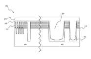
- FIG. 2is a cross-sectional view of a semiconductor substrate 200 .
- the substrateillustrates two configured regions 205 and 207 .
- the substratemay represent the cell region and periphery circuit region of a flash semiconductor substrate.
- a manufacturing processmay be performed to create the structure as illustrated in the figure, and described herein.
- An insulating layer of dielectric material 210may be deposited on the substrate regions 205 , 207 and may serve as an insulating layer, or tunnel oxide as it is referred for a cell region and a gate insulating layer in a peripheral region.
- the tunnel oxide 210may be a high quality dielectric such as a thermal oxide, or may alternatively be deposited by other HDP-CVD or LPCVD processes.
- the tunnel oxide 210may be any high quality oxide, and may be, for example, a thermally grown silicon oxide.
- gate electrodesmay be formed in both the cell region and the peripheral circuit region.
- a floating gate material 215may be deposited on the tunnel oxide 210 .
- the floating gate material 215may be a polysilicon, silicon nitride, silicon oxide, or silicon oxy-nitride, a metalized oxide, or another material that may limit back-tunneling of stored charge.
- the floating gate material 215may be deposited by an HDP-CVD, LPCVD, PVD, or other process for depositing suitable films.
- trenchesmay be etched in both the cell region 205 and the peripheral circuit region 207 .
- the trenchesmay be of various depths and widths, and may be from less than about 10 nm in width to more than about 2 ⁇ m in width.
- the trenches etched in the cell regionmay have cell widths that are less than about 200 nm, and may also be less than about 150 nm, about 100 nm, about 80 nm, about 60 nm, about 50 nm, about 40 nm, about 30 nm, about 20 nm, about 10 nm, etc. or less.
- the trenches in the periphery circuit regionmay have cell widths that are greater than about 100 nm, and may also be greater than about 150 nm, about 200 nm, about 350 nm, about 500 nm, about 750 nm, about 1 ⁇ m, about 1.5 ⁇ m, about 2 ⁇ m, etc. or more.
- the patterningmay be performed simultaneously over both the dense cell region as well as the peripheral circuit region thereby reducing the number of processing steps required for the manufacturing of the substrate.
- the trenches etched in the structuremay vary between the cell region and the peripheral circuit region.
- the trenches etched in the cell regionmay have trench widths that are less than about 50 nanometers, while the trenches etched in the peripheral circuit region may have trench widths that are greater than about 150 nm wide.
- a dielectric material 220may be deposited to create isolation regions on the semiconductor substrate.
- the dielectricmay be deposited simultaneously on both the dense cell region of the substrate and the peripheral region that may contain wider trenches.
- the dielectric material 220may exhibit a balance between flowable and conformal properties so that it may display the following properties: the dielectric may substantially fill the trenches in the dense cell region without producing voids or seams, and may also form a layer of dielectric in the peripheral region that may fill trenches of different width to a substantially equivalent height.
- the filling of the dense cell regions without voids and seamsmay be performed by utilizing a dielectric material that displays flowable properties upon deposition such that a portion of the dielectric material deposited near the top of the trench flows toward the bottom.
- the dielectric materialmay also be limited in the flowable properties such that dielectric material deposited in the peripheral circuit region may fill asymmetrical trenches to a substantially equivalent height.
- the balance of propertiesmay be provided by increasing the amount of a radical precursor gas and carrier gas, which provides a more conformal deposition to a flowable film.
- a second layer of dielectric material 225may be deposited that fills the trenches in the peripheral region as well as completing the filling of any trenches in the cell region that were not filled by the initial dielectric material 220 .
- the capping layer 225may be deposited in the same or a different manner as dielectric 220 , and may be deposited via HARP or E-HARP, for example.
- additional processing stepsmay be performed. For example, an etching or planarization step may be performed in order to remove excess material and expose the floating gate dielectric 215 in the cell region 205 .
- An inter-gate dielectricmay be deposited thereon in preparation for the deposition of a control gate to create a stacked gate structure in the cell region.
- the peripheral circuit regionmay contain electrodes of a single gate structure. Additional materials may then be deposited to form additional layers of structure.
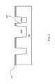
- the peripheral region 207may have multiple trenches etched, as illustrated in FIG. 3 .
- the peripheral circuit region 207may include two trenches of unequal width 350 A, 350 B that are located adjacently to one another. The trenches are thus separated by an unetched portion of the semiconductor substrate 309 .
- flowable dielectricsmay deposit a certain volume of dielectric material, if a general flowable dielectric were deposited in the trenches, the wider trench 350 A may not be filled to the same height as the other trench 350 B, because the same amount of dielectric deposited in each trench would fill to a disparate height. Were this to happen, when the deposited film was cured, an unequal stress may be imposed on each side of the unetched portion of the semiconductor substrate 309 .
- the unequal stressmay create stacking faults or dislocation within the silicon lattice, or may even cause the structure 309 to deform.
- the dielectric material that may be used in the trenchesmay be less flowable so that the dielectric material fills the trenches of unequal width 350 A, 350 B to a substantially similar height, although the material may still display flowable properties.
- FIG. 4shows a method 400 for reducing dislocation caused by a deposited dielectric material on a semiconductor substrate.
- the semiconductor substratemay be an unpatterned or patterned substrate, e.g. an unpatterned 300 mm silicon wafer for use as a nonvolatile semiconductor memory device such as a NAND type flash device.
- the methodmay initially include the optional step 410 of depositing material on the semiconductor substrate.
- the deposition 410may include an initial layer of dielectric material that may function as a tunnel oxide, for example.
- a gate materialsuch as, for example, polysilicon may be deposited on the tunnel oxide. Additional protective material and mask material may be deposited to form a pattern for etching.
- Trenchesmay be etched 415 that create trenches for use in both a cell region of the substrate as well as a peripheral circuit region on the substrate.
- the trenchesmay be of various widths, and the trenches in the peripheral circuit region may be wider than the trenches etched in the cell region.
- the trenchesmay be etched in both the cell region and the peripheral circuit region simultaneously to limit the number of processing steps required overall.
- the trenches etched in the peripheral regionmay include two adjacent trenches of unequal width that are separated by an unetched portion of the semiconductor substrate.
- a dielectric layermay be formed 420 over the semiconductor substrate on both the cell region and the peripheral circuit region.
- the dielectric materialmay be deposited by a CVD process and display flowable properties such that a portion of the dielectric material deposited near the top of a trench flows toward the bottom. Additionally, the dielectric material may form in the peripheral circuit region such that the adjacent trenches of unequal width are filled to a substantially similar height.
- the dielectricmay be densified 425 to convert the structure that may include Si—H and Si—N bonds to Si—O bond, and reduce the porosity of the dielectric material.
- the densificationmay include a curing performed in an ozone environment as well as an annealing performed in a steam environment.
- the curing and annealingmay be performed while the temperature of the substrate is maintained below about 600° C., or alternatively below about 500° C., about 400° C., about 300° C., about 200° C., about 100° C., etc. or less.
- the curing stepmay be performed while the temperature of the substrate is maintained between about 100° C. and about 300° C., or between about 150° C.
- the annealing stepmay be performed while the temperature of the substrate is maintained between about 100° C. and about 500° C., or between about 200° C. and about 400° C.
- the densificationmay result in a shrinkage of the deposited dielectric.
- the materialmay impose a tensile stress on the surrounding substrate structure.
- the lattice structure of the substratemay deform to an extent to address the imposed stress, and may shift to accommodate the stress.
- the competing stresses of differing magnitudemay cause dislocations and/or stacking faults in the underlying structure, which may cause the substrate to deform or collapse.
- the height of the dielectric material deposited in the trenchesmay be substantially equal to reduce the chance of deformation.
- Additional dielectric materialsmay be deposited 430 to fill any remaining trench volume on the substrate.
- the additional materialmay be deposited by a similar process, or alternatively may be deposited with a separate deposition technique such as, for example, a CVD technique such as E-HARP.
- the additional materialmay also be annealed after deposition and, the annealing may be performed above about 600° C., or alternatively above about 700° C., about 800° C., about 900° C., about 1000° C., about 1200° C., etc. or more.
- the methodsmay include etching a plurality of trenches on a semiconductor substrate to form a pattern.
- the patternmay have a cell region of the substrate and a periphery circuit region of the substrate.
- the plurality of trenchesmay include at least two trenches in the periphery circuit region that are of unequal width and are located adjacent to each other such that an unetched portion of the substrate separates the two trenches.
- the plurality of trenchesmay also include at least one trench in the cell region of the substrate.
- the methodsmay include flowing a plurality of precursor gases into the deposition chamber, where the precursor gases include a silicon containing precursor, a nitrogen containing precursor, and an inert carrier gas.
- the flow rate of the nitrogen containing precursormay be at least about two times the flow rate of the silicon containing precursor, and the flow rate of the inert carrier gas may be at least about five times the flow rate of the silicon containing precursor.
- the methodsmay also include forming a layer of dielectric material on the semiconductor substrate on both the cell region and the periphery circuit region simultaneously. The dielectric material may be initially flowable upon deposition so that a portion of the dielectric material deposited near the top of a trench flows toward the bottom of the trench. The methods may further include subsequently densifying the layer of dielectric material.
- the precursor gasesmay include a silicon-based precursor, and may include silyl-amines such as H 2 N(SiH 3 ), HN(SiH 3 ) 2 , and N(SiH 3 ) 3 , among other silyl-amines. These silyl-amines may be mixed with additional gases that may act as carrier gases, reactive gases, or both. Examples of carbon-free silicon precursors may also include silane (SiH 4 ) either alone or mixed with other silicon (e.g., N(SiH 3 ) 3 ), hydrogen (e.g., H 2 ), and/or nitrogen (e.g., N 2 , NH 3 ) containing gases.
- silaneSiH 4
- other silicone.g., N(SiH 3 ) 3
- hydrogene.g., H 2
- nitrogene.g., N 2 , NH 3
- the silicon-containing precursorsmay also include silicon compounds that have no carbon or nitrogen, such as silane, disilane, etc. If the deposited oxide film is a doped oxide film, dopant precursors may also be used such as TEB, TMB, B 2 H 6 , TEPO, PH 3 , P 2 H 6 , and TMP, among other boron and phosphorous dopants.
- the flow rate of the silicon precursormay be greater than or about 100 sccm, greater than or about 200 sccm, greater than or about 250 sccm, greater than or about 275 sccm, greater than or about 300 sccm, greater than or about 350 sccm, greater than or about 400 sccm, etc. or more in different embodiments
- the precursorsmay include a nitrogen based precursor, and may include nitrogen as a radical precursor that passes through a remote plasma region prior to entering into the deposition chamber.
- nitrogenWhen nitrogen is present in the radical precursor, it may be referred to as a radical-nitrogen precursor.
- the radical-nitrogen precursorincludes plasma effluents created by exciting a more stable nitrogen-containing precursor in a plasma.
- a relatively stable nitrogen-containing precursor containing NH 3 and/or hydrazine (N 2 H 4 )may be activated in a chamber plasma region or a remote plasma system (RPS) outside the processing chamber to form the radical-nitrogen precursor, which is then transported into a plasma-free substrate processing region.
- RPSremote plasma system
- the stable nitrogen precursormay also be a mixture comprising NH 3 and N 2 ; NH 3 and H 2 ; NH 3 , N 2 , and H 2 ; and N 2 and H 2 , in different embodiments. Hydrazine may also be used in place of or in combination with NH 3 in the mixtures with N 2 and H 2 .
- the flow rate of the stable nitrogen precursormay be greater than or about 300 sccm, greater than or about 400 sccm, greater than or about 500 sccm, greater than or about 600 sccm, greater than or about 650 sccm, greater than or about 700 sccm, greater than or about 750 sccm, greater than or about 800 sccm, etc.
- Nitrogen-containing precursorsmay also include N 2 O, NO, NO 2 and NH 4 OH.
- the radical-nitrogen precursor producedmay include one or more of —N, —NH, —NH 2 , etc., and may also be accompanied by ionized species formed in the plasma.
- the radical-nitrogen precursoris generated in a section of the processing chamber partitioned from the substrate processing region where the precursors mix and react to deposit the silicon-and-nitrogen layer on a deposition substrate (e.g., a semiconductor wafer).
- the partitionmay be interchangeably referred to as a showerhead.
- the radical-nitrogen precursormay also be accompanied by a carrier gas such as argon, helium, etc.
- the flowabilitymay be due, at least in part, to a significant hydrogen component in the deposited film.
- the deposited filmmay have a silazane-type, Si—NH—Si backbone (i.e., a Si—N—H film).
- Flowabilitymay also result from short chained polymers of the silazane type.
- the nitrogen which allows the formation of short chained polymers and flowabilitymay originate from either the radical precursor or the silicon-containing precursor.
- both the silicon precursor and the radical-nitrogen precursorare carbon-free
- the deposited silicon-and-nitrogen-containing filmis also substantially carbon-free.
- carbon-freedoes not necessarily mean the film lacks even trace amounts of carbon.
- Carbon contaminantsmay be present in the precursor materials that find their way into the deposited silicon-and-nitrogen-containing film. The amount of these carbon impurities however are much less than would be found in a silicon precursor having a carbon moiety (e.g., TEOS, TMDSO, etc.).
- a silicon precursor having a carbon moietye.g., TEOS, TMDSO, etc.
- One or more additional gases and carrier gasesmay be included with the precursors, such as O 2 , H 2 O, Ar, H 2 , N 2 , He, etc., and may have a flow rate that is greater than or about 100 sccm.
- the one or more carrier gasesmay have a flow rate that is greater than or about 200 sccm, greater than or about 500 sccm, greater than or about 750 sccm, greater than or about 1000 sccm, greater than or about 1500 sccm, greater than or about 2000 sccm, greater than or about 2500 sccm, greater than or about 3000 sccm, greater than or about 3500 sccm, etc. or more.
- Additional gasesincluding molecular oxygen, ozone, and/or water vapor may be included with the precursor gases as well.
- the ability to produce a substantially conformal film that displays flowable film propertiesmay be a result of an increase of ammonia radicals during the deposition process.
- the increase in ammonia radicalsmay be as a result of increasing the amount of ammonia and carrier gas delivered to the processing chamber.
- the increased amount of ammoniaprovides additional gas from which the radicals may be formed, and the increased amount of carrier gas may allow for a greater amount of dissociation from the ammonia.
- an enhanced amount of ammonia radialsmay be created and may produce a more conformal film when deposited.
- a conformal film that displays flowable propertiesmay be produced from the precursor gases as a function of the silicon precursor gas used.
- the nitrogen containing precursorwhich may be ammonia in one embodiment, may have a flow rate that is at least about two times the flow rate of the silicon containing precursor.
- the nitrogen containing precursormay be at least about 2.1, about 2.2, about 2.3, about 2.4, about 2.5, about 2.6, about 2.7, about 2.8, about 2.9, about 3, about 3.5, about 4, or about 5 times the flow rate of the silicon containing precursor.
- the carrier gasmay be at least about five times the flow rate of the silicon containing precursor.
- the carrier gasmay be at least about 6, about 7, about 8, about 9, about 10, about 11, about 12, about 13, about 15, about 17, about 20, or about 25 times the flow rate of the silicon containing precursor.
- the depositionmay be performed in a deposition chamber in which the temperature of the substrate is maintained below about 600° C., or alternatively below about 500° C., about 400° C., about 300° C., about 200° C., about 100° C., about 75° C., about 65° C., about 50° C., about 40° C., about 30° C., etc. or less.
- the pressure maintained in the chambermay be at or below about 760 Torr, and may alternatively be below about 600 Torr, about 400 Torr, about 200 Torr, about 100 Torr, about 50 Torr, about 25 Torr, about 15 Torr, about 10 Torr, about 8 Torr, about 6 Torr, about 5 Torr, about 4 Torr, about 3 Torr, about 2 Torr, about 1 Torr, about 0.5 Torr, etc. or less.
- a processmay correspond to a method, a function, a procedure, a subroutine, a subprogram, etc. When a process corresponds to a function, its termination corresponds to a return of the function to the calling function or the main function.
Landscapes
- Engineering & Computer Science (AREA)
- Physics & Mathematics (AREA)
- Microelectronics & Electronic Packaging (AREA)
- General Physics & Mathematics (AREA)
- Manufacturing & Machinery (AREA)
- Computer Hardware Design (AREA)
- Condensed Matter Physics & Semiconductors (AREA)
- Power Engineering (AREA)
- Plasma & Fusion (AREA)
- Chemical & Material Sciences (AREA)
- Chemical Kinetics & Catalysis (AREA)
- Element Separation (AREA)
- Formation Of Insulating Films (AREA)
- Chemical Vapour Deposition (AREA)
Abstract
Description
This application claims the benefit of U.S. Provisional Application No. 61/557,249, filed Nov. 8, 2011, entitled “Methods of Reducing Substrate Dislocation During Gapfill Processing,” the entire disclosure of which is hereby incorporated by reference for all purposes.
The present technology is related to semiconductor manufacturing processes and equipment. More specifically, the present technology is related to semiconductor processing techniques that reduce silicon lattice dislocation in an underlying substrate.
Semiconductor device geometries have dramatically decreased in size since their introduction decades ago. Modern semiconductor fabrication equipment routinely produces devices with 45 nm, 32 nm, and 28 nm feature sizes, and new equipment is being developed and implemented to make devices with even smaller geometries. The decreasing feature sizes result in structural features on the device having decreased spatial dimensions. The widths of gaps and trenches on the device have narrowed to a point where the aspect ratio of gap depth to width becomes high enough to make it challenging to fill the gap with dielectric material. Additionally, the portions of the substrate remaining between the gaps and separating them are becoming even thinner.
When dielectric materials are deposited within and over these gaps, they affect the underlying substrate. For example, when a curing operation is performed, some dielectric materials will shrink to an extent, or densify, which may produce a force on the underlying substrate. When gaps of differing widths lie adjacent to one another, unequal forces may be imposed on opposite sides of the divide based on the amount of deposited material.
Thus, there is a need for new fabrication processes and materials that may adequately fill substrate gaps, while maintaining the substrate feature profiles. These and other benefits are provided by the disclosed technology.
Methods of reducing dislocation in a semiconductor substrate between asymmetrical trenches are described. The methods may include etching a plurality of trenches on a semiconductor substrate and may include two adjacent trenches of unequal width separated by an unetched portion of the substrate. The methods may include forming a layer of dielectric material on the substrate. The dielectric material may form a layer in the trenches located adjacent to each other of substantially equivalent height on both sides of the unetched portion of the substrate separating the two trenches. The methods may include densifying the layer of dielectric material so that the densified dielectric within the two trenches of unequal width exerts a substantially similar stress on the unetched portion of the substrate that separates them.
The methods may further include forming the dielectric material over the entire semiconductor substrate during a simultaneous deposition process step. At least one trench etched in the substrate may have a width of less than or about 100 nm, or less than or about 50 nm, and the two trenches of unequal width may have a trench width greater than or about 100 nm, or greater than or about 150 nm.
The dielectric material may be initially flowable when it is deposited on the semiconductor substrate, so that a portion of the dielectric material deposited at the top of a trench flows toward the bottom of the trench. The temperature of the substrate during the forming of the dielectric layer may be maintained below about 100° C., and the processing chamber in which the forming the dielectric occurs may be maintained at a pressure at or below about 50 Torr. In disclosed embodiments the temperature of the substrate during the forming of the dielectric layer may be maintained below about 50° C., and the processing chamber in which the forming the dielectric occurs may be maintained at a pressure at or below about 5 Torr.
The densifying performed may include curing the dielectric material in an ozone (O3) environment, and then annealing the cured dielectric material in a steam environment. The temperature of the substrate during the curing and annealing may be maintained at or below about 400° C., and may be maintained at or below about 200° C. in disclosed embodiments.
The forming of the dielectric layer may further comprise flowing a nitrogen-containing precursor into the semiconductor deposition chamber in which the etched semiconductor substrate resides, and flowing a silicon-containing precursor into the deposition chamber to come into contact with the nitrogen-containing precursor over the etched semiconductor substrate. The nitrogen-containing precursor may include ammonia, and the nitrogen-containing precursor may have been flowed through a remote plasma region prior to entering the semiconductor deposition chamber to create ammonia radicals.
Methods of forming a layer of dielectric material on a patterned semiconductor substrate are also described. The methods may include etching a plurality of trenches on a semiconductor substrate and may include two adjacent trenches of unequal width separated by an unetched portion of the substrate. The methods may include flowing a plurality of precursor gases into the deposition chamber, where the precursor gases include a silicon-containing precursor, a nitrogen-containing precursor, and an inert carrier gas. The flow rate of the nitrogen-containing precursor may be at least about two times the flow rate of the silicon-containing precursor, and the flow rate of the inert carrier gas may be at least about five times the flow rate of the silicon-containing precursor. The methods may include forming a layer of dielectric material on the substrate. The dielectric material may be initially flowable upon deposition so that a portion of the dielectric material deposited near the top of a trench flows toward the bottom of the trench. The methods may further include densifying the layer of dielectric material so that the densified dielectric within the two trenches of unequal width exerts a substantially similar stress on the unetched portion of the substrate that separates them.
Additional embodiments and features are set forth in part in the description that follows, and in part will become apparent to those skilled in the art upon examination of the specification or may be learned by the practice of the technology. The features and advantages of the technology may be realized and attained by means of the instrumentalities, combinations, and methods described in the specification.
A further understanding of the nature and advantages of the disclosed embodiments may be realized by reference to the remaining portions of the specification and the drawings.
In the appended figures, similar components and/or features may have the same numerical reference label. Further, various components of the same type may be distinguished by following the reference label by a letter that distinguishes among the similar components and/or features. If only the first numerical reference label is used in the specification, the description is applicable to any one of the similar components and/or features having the same first numerical reference label irrespective of the letter suffix.
Methods are described herein for reducing dislocation of a silicon lattice in a semiconductor substrate on which trench filling is performed simultaneously in both dense and less densely patterned regions. The methods allow for the forming of a dielectric layer on a semiconductor substrate that has both a densely patterned region as well as a region having wider trenches. The two regions may have the dielectric material formed simultaneously in a single deposition processing step. The deposition may allow the trenches in the dense region to be substantially filled with the dielectric material without the formation of voids or seams, while filling wider trenches in the other region to a substantially equivalent height. A substantially equivalent height, regardless of the width of the trenches, may provide a reduction of dislocation of the substrate in the region with wider trenches during a subsequent densification of the dielectric material.
Dielectric layers deposited on substrates during semiconductor fabrication may take a variety of forms. For example, more flowable films may be used to fill narrow gaps, but may deposit a less dense, lower quality film. Conformal films may be used to fill wider trenches with a denser dielectric layer, but may create voids or seams if utilized for filling narrow trenches. Another potential issue with some flowable films is that if a thick film is deposited, subsequent densification of the film may create large stresses that are imposed on the underlying substrate. By creating a more conformal dielectric film that also possesses flowable properties, a dielectric may be formed that fills a narrow trench without voids, while at the same time produces a substantially conformal fill of wider trenches.
For example, as shown inFIG. 1A , asemiconductor substrate 100 may have a region with severalnarrow trenches wider trenches narrow gaps wider trenches wide trench 101D may be filled to a greater height thanwider trench 101C. Because flowable films have a lower density, the subsequent densification of the film may be accompanied by film shrinkage. As the film shrinks, a stress is imposed on the underlying substrate. The more material that shrinks, i.e. a trench that is filled to a greater height, the more stress may be imposed on the substrate. Hence for trenches ofunequal width trenches 103 may have a disproportionate stress imposed on each side due to the unequal height of the fill. If the stress is great enough, the structure of the substrate, e.g., a silicon lattice, may have deformation occur or stacking faults form, which may weaken the integrity of the substrate. In more extreme cases, this deformation may result inunetched portion 103 collapsing.
Alternatively, as shown inFIG. 1B , the same substrate trenches may be filled with a more conventional conformal film that fills trenches from the sidewalls in toward the center, regardless of the width of the trench. A higher quality film may be formed that fillswider trenches substrate 103 between the two trenches. However, in thenarrower trenches
Methods of reducing dislocation in a semiconductor substrate between asymmetrical trenches are described. The methods may include etching a plurality of trenches on a semiconductor substrate, and may include two adjacent trenches of unequal width that are separated by an unetched portion of the substrate. The methods may further include forming a layer of dielectric material on the substrate. The dielectric material may form a substantially uniform layer in the trenches so that the two trenches of unequal width are filled to a substantially equivalent height on both sides of the unetched portion of the substrate separating them. The methods may include densifying the layer of dielectric material so that the densified dielectric within the two trenches of unequal width exerts a substantially similar stress on the unetched portion of the substrate that separates them.
For semiconductor substrates used for flash devices such as NAND type flash, gate electrodes may be formed in both the cell region and the peripheral circuit region. A floatinggate material 215 may be deposited on thetunnel oxide 210. The floatinggate material 215 may be a polysilicon, silicon nitride, silicon oxide, or silicon oxy-nitride, a metalized oxide, or another material that may limit back-tunneling of stored charge. The floatinggate material 215 may be deposited by an HDP-CVD, LPCVD, PVD, or other process for depositing suitable films.
Subsequent deposition of protective layers such as a nitride stop-layer, and an oxide mask layer (neither shown) may be deposited. The mask layer may be deposited to create a pattern for the isolation of structures on the substrate. As shown inFIG. 2 , trenches may be etched in both thecell region 205 and theperipheral circuit region 207. The trenches may be of various depths and widths, and may be from less than about 10 nm in width to more than about 2 μm in width. The trenches etched in the cell region may have cell widths that are less than about 200 nm, and may also be less than about 150 nm, about 100 nm, about 80 nm, about 60 nm, about 50 nm, about 40 nm, about 30 nm, about 20 nm, about 10 nm, etc. or less. The trenches in the periphery circuit region may have cell widths that are greater than about 100 nm, and may also be greater than about 150 nm, about 200 nm, about 350 nm, about 500 nm, about 750 nm, about 1 μm, about 1.5 μm, about 2 μm, etc. or more.
The patterning may be performed simultaneously over both the dense cell region as well as the peripheral circuit region thereby reducing the number of processing steps required for the manufacturing of the substrate. The trenches etched in the structure may vary between the cell region and the peripheral circuit region. For example, the trenches etched in the cell region may have trench widths that are less than about 50 nanometers, while the trenches etched in the peripheral circuit region may have trench widths that are greater than about 150 nm wide.
After the trenches have been etched, adielectric material 220 may be deposited to create isolation regions on the semiconductor substrate. The dielectric may be deposited simultaneously on both the dense cell region of the substrate and the peripheral region that may contain wider trenches. Thedielectric material 220 may exhibit a balance between flowable and conformal properties so that it may display the following properties: the dielectric may substantially fill the trenches in the dense cell region without producing voids or seams, and may also form a layer of dielectric in the peripheral region that may fill trenches of different width to a substantially equivalent height. The filling of the dense cell regions without voids and seams may be performed by utilizing a dielectric material that displays flowable properties upon deposition such that a portion of the dielectric material deposited near the top of the trench flows toward the bottom. The dielectric material may also be limited in the flowable properties such that dielectric material deposited in the peripheral circuit region may fill asymmetrical trenches to a substantially equivalent height. The balance of properties may be provided by increasing the amount of a radical precursor gas and carrier gas, which provides a more conformal deposition to a flowable film.
After thedielectric material 220 has been deposited, a second layer ofdielectric material 225, or a capping layer, may be deposited that fills the trenches in the peripheral region as well as completing the filling of any trenches in the cell region that were not filled by the initialdielectric material 220. Thecapping layer 225 may be deposited in the same or a different manner as dielectric220, and may be deposited via HARP or E-HARP, for example. Subsequent to the deposition of the dielectric material layers, additional processing steps may be performed. For example, an etching or planarization step may be performed in order to remove excess material and expose the floatinggate dielectric 215 in thecell region 205. An inter-gate dielectric may be deposited thereon in preparation for the deposition of a control gate to create a stacked gate structure in the cell region. The peripheral circuit region may contain electrodes of a single gate structure. Additional materials may then be deposited to form additional layers of structure.
Theperipheral region 207 may have multiple trenches etched, as illustrated inFIG. 3 . For example, theperipheral circuit region 207 may include two trenches ofunequal width semiconductor substrate 309. Because flowable dielectrics may deposit a certain volume of dielectric material, if a general flowable dielectric were deposited in the trenches, thewider trench 350A may not be filled to the same height as theother trench 350B, because the same amount of dielectric deposited in each trench would fill to a disparate height. Were this to happen, when the deposited film was cured, an unequal stress may be imposed on each side of the unetched portion of thesemiconductor substrate 309. In certain scenarios, the unequal stress may create stacking faults or dislocation within the silicon lattice, or may even cause thestructure 309 to deform. Thus, the dielectric material that may be used in the trenches may be less flowable so that the dielectric material fills the trenches ofunequal width
Trenches may be etched415 that create trenches for use in both a cell region of the substrate as well as a peripheral circuit region on the substrate. The trenches may be of various widths, and the trenches in the peripheral circuit region may be wider than the trenches etched in the cell region. The trenches may be etched in both the cell region and the peripheral circuit region simultaneously to limit the number of processing steps required overall. The trenches etched in the peripheral region may include two adjacent trenches of unequal width that are separated by an unetched portion of the semiconductor substrate.
A dielectric layer may be formed420 over the semiconductor substrate on both the cell region and the peripheral circuit region. The dielectric material may be deposited by a CVD process and display flowable properties such that a portion of the dielectric material deposited near the top of a trench flows toward the bottom. Additionally, the dielectric material may form in the peripheral circuit region such that the adjacent trenches of unequal width are filled to a substantially similar height.
Subsequent to the deposition of the dielectric material, the dielectric may be densified425 to convert the structure that may include Si—H and Si—N bonds to Si—O bond, and reduce the porosity of the dielectric material. The densification may include a curing performed in an ozone environment as well as an annealing performed in a steam environment. The curing and annealing may be performed while the temperature of the substrate is maintained below about 600° C., or alternatively below about 500° C., about 400° C., about 300° C., about 200° C., about 100° C., etc. or less. Alternatively, the curing step may be performed while the temperature of the substrate is maintained between about 100° C. and about 300° C., or between about 150° C. and about 200° C. The annealing step may be performed while the temperature of the substrate is maintained between about 100° C. and about 500° C., or between about 200° C. and about 400° C. The densification may result in a shrinkage of the deposited dielectric. As the material shrinks, the material may impose a tensile stress on the surrounding substrate structure. The lattice structure of the substrate may deform to an extent to address the imposed stress, and may shift to accommodate the stress. In areas where a disproportionate stress is imposed on the same structure, such as, for example, in adjacent trenches of unequal width, the competing stresses of differing magnitude may cause dislocations and/or stacking faults in the underlying structure, which may cause the substrate to deform or collapse. Thus, the height of the dielectric material deposited in the trenches may be substantially equal to reduce the chance of deformation.
Additional dielectric materials may be deposited430 to fill any remaining trench volume on the substrate. The additional material may be deposited by a similar process, or alternatively may be deposited with a separate deposition technique such as, for example, a CVD technique such as E-HARP. The additional material may also be annealed after deposition and, the annealing may be performed above about 600° C., or alternatively above about 700° C., about 800° C., about 900° C., about 1000° C., about 1200° C., etc. or more.
Methods are also described for forming a layer of dielectric material on a patterned semiconductor substrate. The methods may include etching a plurality of trenches on a semiconductor substrate to form a pattern. The pattern may have a cell region of the substrate and a periphery circuit region of the substrate. The plurality of trenches may include at least two trenches in the periphery circuit region that are of unequal width and are located adjacent to each other such that an unetched portion of the substrate separates the two trenches. The plurality of trenches may also include at least one trench in the cell region of the substrate. The methods may include flowing a plurality of precursor gases into the deposition chamber, where the precursor gases include a silicon containing precursor, a nitrogen containing precursor, and an inert carrier gas. The flow rate of the nitrogen containing precursor may be at least about two times the flow rate of the silicon containing precursor, and the flow rate of the inert carrier gas may be at least about five times the flow rate of the silicon containing precursor. The methods may also include forming a layer of dielectric material on the semiconductor substrate on both the cell region and the periphery circuit region simultaneously. The dielectric material may be initially flowable upon deposition so that a portion of the dielectric material deposited near the top of a trench flows toward the bottom of the trench. The methods may further include subsequently densifying the layer of dielectric material.
The precursor gases may include a silicon-based precursor, and may include silyl-amines such as H2N(SiH3), HN(SiH3)2, and N(SiH3)3, among other silyl-amines. These silyl-amines may be mixed with additional gases that may act as carrier gases, reactive gases, or both. Examples of carbon-free silicon precursors may also include silane (SiH4) either alone or mixed with other silicon (e.g., N(SiH3)3), hydrogen (e.g., H2), and/or nitrogen (e.g., N2, NH3) containing gases. The silicon-containing precursors may also include silicon compounds that have no carbon or nitrogen, such as silane, disilane, etc. If the deposited oxide film is a doped oxide film, dopant precursors may also be used such as TEB, TMB, B2H6, TEPO, PH3, P2H6, and TMP, among other boron and phosphorous dopants. The flow rate of the silicon precursor may be greater than or about 100 sccm, greater than or about 200 sccm, greater than or about 250 sccm, greater than or about 275 sccm, greater than or about 300 sccm, greater than or about 350 sccm, greater than or about 400 sccm, etc. or more in different embodiments
The precursors may include a nitrogen based precursor, and may include nitrogen as a radical precursor that passes through a remote plasma region prior to entering into the deposition chamber. When nitrogen is present in the radical precursor, it may be referred to as a radical-nitrogen precursor. The radical-nitrogen precursor includes plasma effluents created by exciting a more stable nitrogen-containing precursor in a plasma. For example, a relatively stable nitrogen-containing precursor containing NH3and/or hydrazine (N2H4) may be activated in a chamber plasma region or a remote plasma system (RPS) outside the processing chamber to form the radical-nitrogen precursor, which is then transported into a plasma-free substrate processing region. The stable nitrogen precursor may also be a mixture comprising NH3and N2; NH3and H2; NH3, N2, and H2; and N2and H2, in different embodiments. Hydrazine may also be used in place of or in combination with NH3in the mixtures with N2and H2. The flow rate of the stable nitrogen precursor may be greater than or about 300 sccm, greater than or about 400 sccm, greater than or about 500 sccm, greater than or about 600 sccm, greater than or about 650 sccm, greater than or about 700 sccm, greater than or about 750 sccm, greater than or about 800 sccm, etc. or more in different embodiments. Nitrogen-containing precursors may also include N2O, NO, NO2and NH4OH. The radical-nitrogen precursor produced may include one or more of —N, —NH, —NH2, etc., and may also be accompanied by ionized species formed in the plasma. In other embodiments, the radical-nitrogen precursor is generated in a section of the processing chamber partitioned from the substrate processing region where the precursors mix and react to deposit the silicon-and-nitrogen layer on a deposition substrate (e.g., a semiconductor wafer). The partition may be interchangeably referred to as a showerhead. The radical-nitrogen precursor may also be accompanied by a carrier gas such as argon, helium, etc.
The flowability may be due, at least in part, to a significant hydrogen component in the deposited film. For example the deposited film may have a silazane-type, Si—NH—Si backbone (i.e., a Si—N—H film). Flowability may also result from short chained polymers of the silazane type. The nitrogen which allows the formation of short chained polymers and flowability may originate from either the radical precursor or the silicon-containing precursor. When both the silicon precursor and the radical-nitrogen precursor are carbon-free, the deposited silicon-and-nitrogen-containing film is also substantially carbon-free. Of course, “carbon-free” does not necessarily mean the film lacks even trace amounts of carbon. Carbon contaminants may be present in the precursor materials that find their way into the deposited silicon-and-nitrogen-containing film. The amount of these carbon impurities however are much less than would be found in a silicon precursor having a carbon moiety (e.g., TEOS, TMDSO, etc.).
One or more additional gases and carrier gases may be included with the precursors, such as O2, H2O, Ar, H2, N2, He, etc., and may have a flow rate that is greater than or about 100 sccm. Alternatively, the one or more carrier gases may have a flow rate that is greater than or about 200 sccm, greater than or about 500 sccm, greater than or about 750 sccm, greater than or about 1000 sccm, greater than or about 1500 sccm, greater than or about 2000 sccm, greater than or about 2500 sccm, greater than or about 3000 sccm, greater than or about 3500 sccm, etc. or more. Additional gases including molecular oxygen, ozone, and/or water vapor may be included with the precursor gases as well.
Without being limited to any particular theory, the ability to produce a substantially conformal film that displays flowable film properties may be a result of an increase of ammonia radicals during the deposition process. The increase in ammonia radicals may be as a result of increasing the amount of ammonia and carrier gas delivered to the processing chamber. The increased amount of ammonia provides additional gas from which the radicals may be formed, and the increased amount of carrier gas may allow for a greater amount of dissociation from the ammonia. Hence, an enhanced amount of ammonia radials may be created and may produce a more conformal film when deposited. A conformal film that displays flowable properties may be produced from the precursor gases as a function of the silicon precursor gas used. For example, the nitrogen containing precursor, which may be ammonia in one embodiment, may have a flow rate that is at least about two times the flow rate of the silicon containing precursor. Alternatively, the nitrogen containing precursor may be at least about 2.1, about 2.2, about 2.3, about 2.4, about 2.5, about 2.6, about 2.7, about 2.8, about 2.9, about 3, about 3.5, about 4, or about 5 times the flow rate of the silicon containing precursor. Additionally, the carrier gas may be at least about five times the flow rate of the silicon containing precursor. Alternatively, the carrier gas may be at least about 6, about 7, about 8, about 9, about 10, about 11, about 12, about 13, about 15, about 17, about 20, or about 25 times the flow rate of the silicon containing precursor.
The deposition may be performed in a deposition chamber in which the temperature of the substrate is maintained below about 600° C., or alternatively below about 500° C., about 400° C., about 300° C., about 200° C., about 100° C., about 75° C., about 65° C., about 50° C., about 40° C., about 30° C., etc. or less. The pressure maintained in the chamber may be at or below about 760 Torr, and may alternatively be below about 600 Torr, about 400 Torr, about 200 Torr, about 100 Torr, about 50 Torr, about 25 Torr, about 15 Torr, about 10 Torr, about 8 Torr, about 6 Torr, about 5 Torr, about 4 Torr, about 3 Torr, about 2 Torr, about 1 Torr, about 0.5 Torr, etc. or less.
In the preceding description, for the purposes of explanation, numerous details have been set forth in order to provide an understanding of various embodiments of the present invention. It will be apparent to one skilled in the art, however, that certain embodiments may be practiced without some of these details, or with additional details.
Having disclosed several embodiments, it will be recognized by those of skill in the art that various modifications, alternative constructions, and equivalents may be used without departing from the spirit of the disclosed embodiments. Additionally, a number of well known processes and elements have not been described in order to avoid unnecessarily obscuring the present invention. Accordingly, the above description should not be taken as limiting the scope of the invention.
It is noted that individual embodiments may be described as a process which is depicted as a flowchart, a flow diagram, or a block diagram. Although a flowchart may describe the method as a sequential process, many of the operations may be performed in parallel or concurrently. In addition, the order of the operations may be rearranged. A process may be terminated when its operations are completed, but could have additional steps not discussed or included in a figure. Furthermore, not all operations in any particularly described process may occur in all embodiments. A process may correspond to a method, a function, a procedure, a subroutine, a subprogram, etc. When a process corresponds to a function, its termination corresponds to a return of the function to the calling function or the main function.
Where a range of values is provided, it is understood that each intervening value between the upper and lower limits of that range is also specifically disclosed, to the smallest fraction of the unit or value of the lower limit, unless the context clearly dictates otherwise. Any encompassed range between any stated value or intervening value in a stated range and any other stated or intervening value in that stated range is disclosed. The upper and lower limits of those smaller ranges may independently be included or excluded in the range, and each range where either, neither, or both limits are included in the smaller range is also disclosed and encompassed within the technology, subject to any specifically excluded limit, value, or encompassed range in the stated range. Where the stated range includes one or both of the limits, ranges excluding either or both of those included limits are also included.
As used herein and in the appended claims, the singular forms “a”, “an”, and “the” include plural references unless the context clearly dictates otherwise. Thus, for example, reference to “a dielectric material” includes a plurality of such materials, and reference to “the process” includes reference to one or more processes and equivalents thereof known to those skilled in the art, and so forth.
Also, the words “comprise”, “comprising”, “include”, “including”, and “includes”, when used in this specification and in the following claims, are intended to specify the presence of stated features, integers, components, or steps, but they do not preclude the presence or addition of one or more other features, integers, components, steps, acts, or groups.
Claims (16)
1. A method of forming a layer of dielectric material on a patterned semiconductor substrate, the method comprising:
etching a plurality of trenches on a semiconductor substrate, wherein the plurality of trenches includes two trenches that are of unequal width and are located adjacent to each other such that an unetched portion of the substrate separates the two trenches of unequal width;
forming a layer of dielectric material on the semiconductor substrate, wherein the dielectric material forms a layer in the trenches located adjacent to each other of substantially equivalent height on both sides of the unetched portion of the substrate separating the two trenches; and
densifying the layer of dielectric material, wherein the densified dielectric within the two trenches of unequal width exerts substantially equal stress on the unetched portion of the substrate;
wherein the densifying comprises:
curing the dielectric material in an ozone (03) environment; and
annealing the cured dielectric material in a steam environment;
wherein the forming of the dielectric layer further comprises:
flowing a nitrogen-containing precursor into a semiconductor deposition chamber in which the etched semiconductor substrate resides; and
flowing a silicon-containing precursor into the deposition chamber to come into contact with the nitrogen-containing precursor over the etched semiconductor substrate.
2. The method ofclaim 1 , wherein the layer of dielectric material is initially formed over the entire semiconductor substrate during a simultaneous deposition process step.
3. The method ofclaim 1 , wherein at least one trench etched in the substrate has a trench width less than about 100 nanometers, and wherein the two trenches of unequal width have a trench width greater than about 100 nanometers.
4. The method ofclaim 3 , wherein at least one trench etched in the substrate has a trench width less than about 50 nanometers, and wherein the two trenches of unequal width have a trench width greater than about 150 nanometers.
5. The method ofclaim 1 , wherein the dielectric material is initially flowable when it is deposited on the semiconductor substrate so that a portion of the dielectric material deposited at the top of a trench flows toward the bottom of the trench.
6. The method ofclaim 1 , wherein the temperature of the substrate during the forming of the dielectric layer is maintained below about 100° C., and wherein the forming of the dielectric layer on the substrate occurs in a processing chamber having a pressure below about 50 Torr.
7. The method ofclaim 6 , wherein the temperature of the substrate during the forming of the dielectric layer is maintained below about 50° C., and wherein the forming of the dielectric layer on the substrate occurs in a processing chamber having a pressure below about 5 Torr.
8. The method ofclaim 1 , wherein the temperature of the substrate during the curing and annealing is maintained at or below about 400° C.
9. The method ofclaim 8 , wherein the temperature of the substrate during the curing is maintained at or below about 200° C.
10. The method ofclaim 1 , wherein the nitrogen-containing precursor is ammonia.
11. The method ofclaim 10 , wherein the ammonia has been flowed through a remote plasma region prior to entering the semiconductor deposition chamber to create ammonia radicals.
12. A method of forming a layer of dielectric material on a patterned semiconductor substrate, the method comprising:
etching a plurality of trenches on a semiconductor substrate, wherein the plurality of trenches includes two trenches that are of unequal width and are located adjacent to each other such that an unetched portion of the substrate separates the two trenches of unequal width;
flowing a plurality of precursor gases into the deposition chamber, wherein:
the precursor gases comprise a silicon containing precursor, a nitrogen containing precursor, and an inert carrier gas,
the flow rate of the nitrogen containing precursor is at least about two times the flow rate of the silicon containing precursor, and
the flow rate of the inert carrier gas is at least about five times the flow rate of the silicon containing precursor;
forming a layer of dielectric material on the semiconductor substrate, wherein the dielectric material is initially flowable upon deposition so that a portion of the dielectric material deposited near the top of a trench flows toward the bottom of the trench; and
densifying the layer of dielectric material;
wherein the formed dielectric layer forms a layer in the trenches located adjacent to each other of substantially equivalent height on both sides of the unetched portion of the substrate separating the two trenches;
wherein the densifying comprises:
curing the dielectric material in an ozone (03) environment; and
annealing the cured dielectric material in a steam environment.
13. The method ofclaim 12 , wherein the densified dielectric within the two trenches of unequal width exerts substantially equal stress on the unetched portion of the substrate.
14. The method ofclaim 12 , wherein the temperature of the substrate during the curing and annealing is maintained at or below about 400° C.
15. The method ofclaim 12 , wherein the nitrogen-containing precursor is ammonia.
16. The method ofclaim 15 , wherein the ammonia has been flowed through a remote plasma region prior to entering the semiconductor deposition chamber to create ammonia radicals.
Priority Applications (1)
| Application Number | Priority Date | Filing Date | Title |
|---|---|---|---|
| US13/669,184US8975152B2 (en) | 2011-11-08 | 2012-11-05 | Methods of reducing substrate dislocation during gapfill processing |
Applications Claiming Priority (2)
| Application Number | Priority Date | Filing Date | Title |
|---|---|---|---|
| US201161557249P | 2011-11-08 | 2011-11-08 | |
| US13/669,184US8975152B2 (en) | 2011-11-08 | 2012-11-05 | Methods of reducing substrate dislocation during gapfill processing |
Publications (2)
| Publication Number | Publication Date |
|---|---|
| US20130309870A1 US20130309870A1 (en) | 2013-11-21 |
| US8975152B2true US8975152B2 (en) | 2015-03-10 |
Family
ID=48290453
Family Applications (1)
| Application Number | Title | Priority Date | Filing Date |
|---|---|---|---|
| US13/669,184Expired - Fee RelatedUS8975152B2 (en) | 2011-11-08 | 2012-11-05 | Methods of reducing substrate dislocation during gapfill processing |
Country Status (3)
| Country | Link |
|---|---|
| US (1) | US8975152B2 (en) |
| TW (1) | TW201330103A (en) |
| WO (1) | WO2013070436A1 (en) |
Cited By (3)
| Publication number | Priority date | Publication date | Assignee | Title |
|---|---|---|---|---|
| US20130149462A1 (en)* | 2011-07-15 | 2013-06-13 | Applied Materials, Inc. | Surface treatment and deposition for reduced outgassing |
| US10490556B1 (en)* | 2018-07-02 | 2019-11-26 | United Microelectronics Corp. | Semiconductor device and method for fabricating the same |
| US11120997B2 (en)* | 2018-08-31 | 2021-09-14 | Taiwan Semiconductor Manufacturing Co., Ltd. | Surface treatment for etch tuning |
Families Citing this family (9)
| Publication number | Priority date | Publication date | Assignee | Title |
|---|---|---|---|---|
| US20150371956A1 (en)* | 2014-06-19 | 2015-12-24 | Globalfoundries Inc. | Crackstops for bulk semiconductor wafers |
| TWI670756B (en)* | 2014-12-22 | 2019-09-01 | 美商應用材料股份有限公司 | Fcvd line bending resolution by deposition modulation |
| KR102442309B1 (en)* | 2015-07-09 | 2022-09-13 | 삼성전자주식회사 | Methods of forming an isolation structure in a semiconductor device |
| US9607997B1 (en)* | 2015-09-08 | 2017-03-28 | Sandisk Technologies Inc. | Metal line with increased inter-metal breakdown voltage |
| US9391081B1 (en)* | 2015-09-08 | 2016-07-12 | Sandisk Technologies Llc | Metal indentation to increase inter-metal breakdown voltage |
| US10224235B2 (en)* | 2016-02-05 | 2019-03-05 | Lam Research Corporation | Systems and methods for creating airgap seals using atomic layer deposition and high density plasma chemical vapor deposition |
| US10410910B1 (en)* | 2018-08-20 | 2019-09-10 | Nanya Technology Corporation | Method for preparing semiconductor structures |
| US11201122B2 (en) | 2018-09-27 | 2021-12-14 | Taiwan Semiconductor Manufacturing Co., Ltd. | Method of fabricating semiconductor device with reduced warpage and better trench filling performance |
| TWI703673B (en)* | 2018-09-27 | 2020-09-01 | 台灣積體電路製造股份有限公司 | Method of fabricating semiconductor device and semiconductor device |
Citations (597)
| Publication number | Priority date | Publication date | Assignee | Title |
|---|---|---|---|---|
| US2369620A (en) | 1941-03-07 | 1945-02-13 | Battelle Development Corp | Method of coating cupreous metal with tin |
| US3451840A (en) | 1965-10-06 | 1969-06-24 | Us Air Force | Wire coated with boron nitride and boron |
| US3937857A (en) | 1974-07-22 | 1976-02-10 | Amp Incorporated | Catalyst for electroless deposition of metals |
| US4006047A (en) | 1974-07-22 | 1977-02-01 | Amp Incorporated | Catalysts for electroless deposition of metals on comparatively low-temperature polyolefin and polyester substrates |
| US4209357A (en) | 1979-05-18 | 1980-06-24 | Tegal Corporation | Plasma reactor apparatus |
| US4214946A (en) | 1979-02-21 | 1980-07-29 | International Business Machines Corporation | Selective reactive ion etching of polysilicon against SiO2 utilizing SF6 -Cl2 -inert gas etchant |
| US4232060A (en) | 1979-01-22 | 1980-11-04 | Richardson Chemical Company | Method of preparing substrate surface for electroless plating and products produced thereby |
| US4234628A (en) | 1978-11-28 | 1980-11-18 | The Harshaw Chemical Company | Two-step preplate system for polymeric surfaces |
| US4265943A (en) | 1978-11-27 | 1981-05-05 | Macdermid Incorporated | Method and composition for continuous electroless copper deposition using a hypophosphite reducing agent in the presence of cobalt or nickel ions |
| US4364803A (en) | 1980-03-11 | 1982-12-21 | Oronzio De Nora Impianti Elettrochimici S.P.A. | Deposition of catalytic electrodes on ion-exchange membranes |
| US4368223A (en) | 1981-06-01 | 1983-01-11 | Asahi Glass Company, Ltd. | Process for preparing nickel layer |
| US4397812A (en) | 1974-05-24 | 1983-08-09 | Richardson Chemical Company | Electroless nickel polyalloys |
| US4468413A (en) | 1982-02-15 | 1984-08-28 | U.S. Philips Corporation | Method of manufacturing fluorine-doped optical fibers |
| US4565601A (en) | 1983-09-12 | 1986-01-21 | Hitachi, Ltd. | Method and apparatus for controlling sample temperature |
| US4571819A (en) | 1984-11-01 | 1986-02-25 | Ncr Corporation | Method for forming trench isolation structures |
| US4579618A (en) | 1984-01-06 | 1986-04-01 | Tegal Corporation | Plasma reactor apparatus |
| US4585920A (en) | 1982-05-21 | 1986-04-29 | Tegal Corporation | Plasma reactor removable insert |
| US4632857A (en) | 1974-05-24 | 1986-12-30 | Richardson Chemical Company | Electrolessly plated product having a polymetallic catalytic film underlayer |
| US4656052A (en) | 1984-02-13 | 1987-04-07 | Kyocera Corporation | Process for production of high-hardness boron nitride film |
| US4690746A (en) | 1986-02-24 | 1987-09-01 | Genus, Inc. | Interlayer dielectric process |
| US4714520A (en) | 1985-07-25 | 1987-12-22 | Advanced Micro Devices, Inc. | Method for filling a trench in an integrated circuit structure without producing voids |
| US4749440A (en) | 1985-08-28 | 1988-06-07 | Fsi Corporation | Gaseous process and apparatus for removing films from substrates |
| US4753898A (en) | 1987-07-09 | 1988-06-28 | Motorola, Inc. | LDD CMOS process |
| US4807016A (en) | 1985-07-15 | 1989-02-21 | Texas Instruments Incorporated | Dry etch of phosphosilicate glass with selectivity to undoped oxide |
| US4810520A (en) | 1987-09-23 | 1989-03-07 | Magnetic Peripherals Inc. | Method for controlling electroless magnetic plating |
| US4816638A (en) | 1987-02-20 | 1989-03-28 | Anelva Corporation | Vacuum processing apparatus |
| US4851370A (en) | 1987-12-28 | 1989-07-25 | American Telephone And Telegraph Company, At&T Bell Laboratories | Fabricating a semiconductor device with low defect density oxide |
| EP0329406A1 (en) | 1988-02-16 | 1989-08-23 | Polyonics Corporation | Metal coated laminate products made from textured polymide film |
| US4865685A (en) | 1987-11-03 | 1989-09-12 | North Carolina State University | Dry etching of silicon carbide |
| US4872947A (en) | 1986-12-19 | 1989-10-10 | Applied Materials, Inc. | CVD of silicon oxide using TEOS decomposition and in-situ planarization process |
| US4886570A (en) | 1987-07-16 | 1989-12-12 | Texas Instruments Incorporated | Processing apparatus and method |
| US4892753A (en) | 1986-12-19 | 1990-01-09 | Applied Materials, Inc. | Process for PECVD of silicon oxide using TEOS decomposition |
| US4894352A (en) | 1988-10-26 | 1990-01-16 | Texas Instruments Inc. | Deposition of silicon-containing films using organosilicon compounds and nitrogen trifluoride |
| US4904341A (en) | 1988-08-22 | 1990-02-27 | Westinghouse Electric Corp. | Selective silicon dioxide etchant for superconductor integrated circuits |
| US4951601A (en) | 1986-12-19 | 1990-08-28 | Applied Materials, Inc. | Multi-chamber integrated process system |
| US4960488A (en) | 1986-12-19 | 1990-10-02 | Applied Materials, Inc. | Reactor chamber self-cleaning process |
| JPH02121330U (en) | 1989-03-15 | 1990-10-02 | ||
| JPH02256235A (en) | 1988-12-27 | 1990-10-17 | Toshiba Corp | Surface treatment method |
| US4981551A (en) | 1987-11-03 | 1991-01-01 | North Carolina State University | Dry etching of silicon carbide |
| US4985372A (en) | 1989-02-17 | 1991-01-15 | Tokyo Electron Limited | Method of forming conductive layer including removal of native oxide |
| US4994404A (en) | 1989-08-28 | 1991-02-19 | Motorola, Inc. | Method for forming a lightly-doped drain (LDD) structure in a semiconductor device |
| US5000113A (en) | 1986-12-19 | 1991-03-19 | Applied Materials, Inc. | Thermal CVD/PECVD reactor and use for thermal chemical vapor deposition of silicon dioxide and in-situ multi-step planarized process |
| US5013691A (en) | 1989-07-31 | 1991-05-07 | At&T Bell Laboratories | Anisotropic deposition of silicon dioxide |
| US5030319A (en) | 1988-12-27 | 1991-07-09 | Kabushiki Kaisha Toshiba | Method of oxide etching with condensed plasma reaction product |
| US5061838A (en) | 1989-06-23 | 1991-10-29 | Massachusetts Institute Of Technology | Toroidal electron cyclotron resonance reactor |
| US5089441A (en) | 1990-04-16 | 1992-02-18 | Texas Instruments Incorporated | Low-temperature in-situ dry cleaning process for semiconductor wafers |
| US5089442A (en) | 1990-09-20 | 1992-02-18 | At&T Bell Laboratories | Silicon dioxide deposition method using a magnetic field and both sputter deposition and plasma-enhanced cvd |
| EP0496543A2 (en) | 1991-01-23 | 1992-07-29 | Nec Corporation | Method of forming silicon oxide film containing fluorine |
| JPH04239723A (en) | 1991-01-23 | 1992-08-27 | Nec Corp | Manufacture of semiconductor device |
| US5147692A (en) | 1990-05-08 | 1992-09-15 | Macdermid, Incorporated | Electroless plating of nickel onto surfaces such as copper or fused tungston |
| US5156881A (en) | 1987-03-18 | 1992-10-20 | Kabushiki Kaisha Toshiba | Method for forming a film on a substrate by activating a reactive gas |
| WO1992020833A1 (en) | 1991-05-17 | 1992-11-26 | Lam Research Corporation | A PROCESS FOR DEPOSITING A SIOx FILM HAVING REDUCED INTRINSIC STRESS AND/OR REDUCED HYDROGEN CONTENT |
| JPH04341568A (en) | 1991-05-16 | 1992-11-27 | Toshiba Corp | Thin film forming method and thin film forming apparatus |
| US5186718A (en) | 1989-05-19 | 1993-02-16 | Applied Materials, Inc. | Staged-vacuum wafer processing system and method |
| US5198034A (en) | 1987-03-31 | 1993-03-30 | Epsilon Technology, Inc. | Rotatable substrate supporting mechanism with temperature sensing device for use in chemical vapor deposition equipment |
| US5203911A (en) | 1991-06-24 | 1993-04-20 | Shipley Company Inc. | Controlled electroless plating |
| US5228501A (en) | 1986-12-19 | 1993-07-20 | Applied Materials, Inc. | Physical vapor deposition clamping mechanism and heater/cooler |
| US5231690A (en) | 1990-03-12 | 1993-07-27 | Ngk Insulators, Ltd. | Wafer heaters for use in semiconductor-producing apparatus and heating units using such wafer heaters |
| US5235139A (en) | 1990-09-12 | 1993-08-10 | Macdermid, Incorprated | Method for fabricating printed circuits |
| US5238499A (en) | 1990-07-16 | 1993-08-24 | Novellus Systems, Inc. | Gas-based substrate protection during processing |
| US5240497A (en) | 1991-10-08 | 1993-08-31 | Cornell Research Foundation, Inc. | Alkaline free electroless deposition |
| US5248527A (en) | 1991-03-01 | 1993-09-28 | C. Uyemura And Company, Limited | Process for electroless plating tin, lead or tin-lead alloy |
| US5252178A (en) | 1992-06-24 | 1993-10-12 | Texas Instruments Incorporated | Multi-zone plasma processing method and apparatus |
| US5270125A (en) | 1989-07-11 | 1993-12-14 | Redwood Microsystems, Inc. | Boron nutride membrane in wafer structure |
| US5271972A (en) | 1992-08-17 | 1993-12-21 | Applied Materials, Inc. | Method for depositing ozone/TEOS silicon oxide films of reduced surface sensitivity |
| US5275977A (en) | 1990-03-19 | 1994-01-04 | Hitachi, Ltd. | Insulating film forming method for semiconductor device interconnection |
| US5279865A (en) | 1991-06-28 | 1994-01-18 | Digital Equipment Corporation | High throughput interlevel dielectric gap filling process |
| US5288518A (en) | 1991-06-07 | 1994-02-22 | Nec Corproation | Chemical vapor deposition method for forming fluorine containing silicon oxide film |
| US5290382A (en) | 1991-12-13 | 1994-03-01 | Hughes Aircraft Company | Methods and apparatus for generating a plasma for "downstream" rapid shaping of surfaces of substrates and films |
| US5302233A (en) | 1993-03-19 | 1994-04-12 | Micron Semiconductor, Inc. | Method for shaping features of a semiconductor structure using chemical mechanical planarization (CMP) |
| US5306530A (en) | 1992-11-23 | 1994-04-26 | Associated Universities, Inc. | Method for producing high quality thin layer films on substrates |
| US5314724A (en) | 1991-01-08 | 1994-05-24 | Fujitsu Limited | Process for forming silicon oxide film |
| US5316804A (en) | 1990-08-10 | 1994-05-31 | Sumitomo Electric Industries, Ltd. | Process for the synthesis of hard boron nitride |
| US5319247A (en) | 1990-10-30 | 1994-06-07 | Mitsubishi Denki Kabushiki Kaisha | Semiconductor device having an interlayer insulating film of high crack resistance |
| US5328810A (en) | 1990-05-07 | 1994-07-12 | Micron Technology, Inc. | Method for reducing, by a factor or 2-N, the minimum masking pitch of a photolithographic process |
| US5328558A (en) | 1992-03-25 | 1994-07-12 | Tokyo Electron Limited | Method for etching an SiO2 film |
| US5334552A (en) | 1991-12-04 | 1994-08-02 | Nec Corporation | Method for fabricating a semiconductor device having a multi-layered interconnection structure |
| US5345999A (en) | 1993-03-17 | 1994-09-13 | Applied Materials, Inc. | Method and apparatus for cooling semiconductor wafers |
| US5352636A (en) | 1992-01-16 | 1994-10-04 | Applied Materials, Inc. | In situ method for cleaning silicon surface and forming layer thereon in same chamber |
| US5368897A (en) | 1987-04-03 | 1994-11-29 | Fujitsu Limited | Method for arc discharge plasma vapor deposition of diamond |
| US5380560A (en) | 1992-07-28 | 1995-01-10 | International Business Machines Corporation | Palladium sulfate solution for the selective seeding of the metal interconnections on polyimide dielectrics for electroless metal deposition |
| US5382311A (en) | 1992-12-17 | 1995-01-17 | Tokyo Electron Limited | Stage having electrostatic chuck and plasma processing apparatus using same |
| US5384284A (en) | 1993-10-01 | 1995-01-24 | Micron Semiconductor, Inc. | Method to form a low resistant bond pad interconnect |
| US5399529A (en) | 1992-05-27 | 1995-03-21 | Nec Corporation | Process for producing semiconductor devices |
| US5403434A (en) | 1994-01-06 | 1995-04-04 | Texas Instruments Incorporated | Low-temperature in-situ dry cleaning process for semiconductor wafer |
| US5416048A (en) | 1993-04-16 | 1995-05-16 | Micron Semiconductor, Inc. | Method to slope conductor profile prior to dielectric deposition to improve dielectric step-coverage |
| US5415890A (en) | 1994-01-03 | 1995-05-16 | Eaton Corporation | Modular apparatus and method for surface treatment of parts with liquid baths |
| JPH07130713A (en) | 1993-11-04 | 1995-05-19 | Fujitsu Ltd | Downflow etching equipment |
| US5420075A (en) | 1992-04-15 | 1995-05-30 | Nec Corporation | Forming multi-layered interconnections with fluorine compound treatment permitting selective deposition of insulator |
| EP0658928A1 (en) | 1993-12-16 | 1995-06-21 | International Business Machines Corporation | Method of plasma etching silicon dioxide, selectively to silicon nitride and polysilicon |
| GB2285174A (en) | 1993-12-27 | 1995-06-28 | Mitsubishi Electric Corp | Via-hole and production method of via-hole |
| US5429995A (en) | 1992-07-17 | 1995-07-04 | Kabushiki Kaisha Toshiba | Method of manufacturing silicon oxide film containing fluorine |
| US5439553A (en) | 1994-03-30 | 1995-08-08 | Penn State Research Foundation | Controlled etching of oxides via gas phase reactions |
| US5451259A (en) | 1994-02-17 | 1995-09-19 | Krogh; Ole D. | ECR plasma source for remote processing |
| US5468342A (en) | 1994-04-28 | 1995-11-21 | Cypress Semiconductor Corp. | Method of etching an oxide layer |
| US5474589A (en) | 1990-11-28 | 1995-12-12 | Sumitomo Electric Industries, Ltd. | UV light-permeable glass and article comprising the same |
| US5478462A (en) | 1987-02-24 | 1995-12-26 | Polyonics Corporation, Inc. | Process for forming polyimide-metal laminates |
| US5483920A (en) | 1993-08-05 | 1996-01-16 | Board Of Governors Of Wayne State University | Method of forming cubic boron nitride films |
| EP0697467A1 (en) | 1994-07-21 | 1996-02-21 | Applied Materials, Inc. | Method and apparatus for cleaning a deposition chamber |
| US5500249A (en) | 1992-12-22 | 1996-03-19 | Applied Materials, Inc. | Uniform tungsten silicide films produced by chemical vapor deposition |
| US5510216A (en) | 1993-08-25 | 1996-04-23 | Shipley Company Inc. | Selective metallization process |
| US5516367A (en) | 1993-04-05 | 1996-05-14 | Applied Materials, Inc. | Chemical vapor deposition chamber with a purge guide |
| JPH08148470A (en) | 1994-11-21 | 1996-06-07 | Sanyo Electric Co Ltd | Manufacture of semiconductor device |
| US5531835A (en) | 1994-05-18 | 1996-07-02 | Applied Materials, Inc. | Patterned susceptor to reduce electrostatic force in a CVD chamber |
| US5534070A (en) | 1993-03-31 | 1996-07-09 | Canon Kabushiki Kaisha | Plasma CVD process using a very-high-frequency and plasma CVD apparatus |
| US5536360A (en) | 1993-04-09 | 1996-07-16 | International Business Machines Corporation | Method for etching boron nitride |
| US5549780A (en) | 1990-10-23 | 1996-08-27 | Semiconductor Energy Laboratory Co., Ltd. | Method for plasma processing and apparatus for plasma processing |
| US5558717A (en) | 1994-11-30 | 1996-09-24 | Applied Materials | CVD Processing chamber |
| US5560779A (en) | 1993-07-12 | 1996-10-01 | Olin Corporation | Apparatus for synthesizing diamond films utilizing an arc plasma |
| US5563105A (en) | 1994-09-30 | 1996-10-08 | International Business Machines Corporation | PECVD method of depositing fluorine doped oxide using a fluorine precursor containing a glass-forming element |
| US5571576A (en) | 1995-02-10 | 1996-11-05 | Watkins-Johnson | Method of forming a fluorinated silicon oxide layer using plasma chemical vapor deposition |
| JPH08306671A (en) | 1995-05-08 | 1996-11-22 | Yasuhiro Horiike | Plasma etching equipment |
| US5578130A (en) | 1990-12-12 | 1996-11-26 | Semiconductor Energy Laboratory Co., Ltd. | Apparatus and method for depositing a film |
| US5591269A (en) | 1993-06-24 | 1997-01-07 | Tokyo Electron Limited | Vacuum processing apparatus |
| US5599740A (en) | 1995-11-16 | 1997-02-04 | Taiwan Semiconductor Manufacturing Company, Ltd. | Deposit-etch-deposit ozone/teos insulator layer method |
| US5624582A (en) | 1993-01-21 | 1997-04-29 | Vlsi Technology, Inc. | Optimization of dry etching through the control of helium backside pressure |
| US5626922A (en) | 1990-09-25 | 1997-05-06 | Semiconductor Energy Laboratory Co., Ltd. | Plasma processing method |
| JPH09153481A (en) | 1995-11-30 | 1997-06-10 | Sumitomo Metal Ind Ltd | Plasma processing equipment |
| US5645645A (en) | 1995-04-07 | 1997-07-08 | Board Of Trustees Operating Michigan State University | Method and apparatus for plasma treatment of a surface |
| US5648125A (en) | 1995-11-16 | 1997-07-15 | Cane; Frank N. | Electroless plating process for the manufacture of printed circuit boards |
| US5648175A (en) | 1996-02-14 | 1997-07-15 | Applied Materials, Inc. | Chemical vapor deposition reactor system and integrated circuit |
| JPH09205140A (en) | 1995-11-21 | 1997-08-05 | Toshiba Corp | Element-isolated semiconductor substrate and manufacturing method thereof |
| US5656093A (en) | 1996-03-08 | 1997-08-12 | Applied Materials, Inc. | Wafer spacing mask for a substrate support chuck and method of fabricating same |
| US5661093A (en) | 1996-09-12 | 1997-08-26 | Applied Materials, Inc. | Method for the stabilization of halogen-doped films through the use of multiple sealing layers |
| US5674787A (en) | 1996-01-16 | 1997-10-07 | Sematech, Inc. | Selective electroless copper deposited interconnect plugs for ULSI applications |
| US5679606A (en) | 1995-12-27 | 1997-10-21 | Taiwan Semiconductor Manufacturing Company, Ltd. | method of forming inter-metal-dielectric structure |
| US5695810A (en) | 1996-11-20 | 1997-12-09 | Cornell Research Foundation, Inc. | Use of cobalt tungsten phosphide as a barrier material for copper metallization |
| US5712185A (en) | 1996-04-23 | 1998-01-27 | United Microelectronics | Method for forming shallow trench isolation |
| US5716500A (en) | 1993-10-18 | 1998-02-10 | Surfcoat Oy | Method and an apparatus for generation of a discharge in own vapors of a radio frequency electrode for sustained self-sputtering and evaporation of the electrode |
| US5716506A (en) | 1995-10-06 | 1998-02-10 | Board Of Trustees Of The University Of Illinois | Electrochemical sensors for gas detection |
| US5719085A (en) | 1995-09-29 | 1998-02-17 | Intel Corporation | Shallow trench isolation technique |
| US5733816A (en) | 1995-12-13 | 1998-03-31 | Micron Technology, Inc. | Method for depositing a tungsten layer on silicon |
| US5747373A (en) | 1996-09-24 | 1998-05-05 | Taiwan Semiconductor Manufacturing Company Ltd. | Nitride-oxide sidewall spacer for salicide formation |
| US5755859A (en) | 1995-08-24 | 1998-05-26 | International Business Machines Corporation | Cobalt-tin alloys and their applications for devices, chip interconnections and packaging |
| US5756402A (en) | 1992-12-28 | 1998-05-26 | Kabushiki Kaisha Toshiba | Method of etching silicon nitride film |
| JPH10178004A (en) | 1996-11-13 | 1998-06-30 | Applied Materials Inc | Method and apparatus for cleaning a surface in a substrate processing system |
| US5781693A (en) | 1996-07-24 | 1998-07-14 | Applied Materials, Inc. | Gas introduction showerhead for an RTP chamber with upper and lower transparent plates and gas flow therebetween |
| US5786276A (en) | 1997-03-31 | 1998-07-28 | Applied Materials, Inc. | Selective plasma etching of silicon nitride in presence of silicon or silicon oxides using mixture of CH3F or CH2F2 and CF4 and O2 |
| US5789300A (en) | 1997-02-25 | 1998-08-04 | Advanced Micro Devices, Inc. | Method of making IGFETs in densely and sparsely populated areas of a substrate |
| US5804259A (en) | 1996-11-07 | 1998-09-08 | Applied Materials, Inc. | Method and apparatus for depositing a multilayered low dielectric constant film |
| US5820723A (en) | 1996-06-05 | 1998-10-13 | Lam Research Corporation | Universal vacuum chamber including equipment modules such as a plasma generating source, vacuum pumping arrangement and/or cantilevered substrate support |
| US5824599A (en) | 1996-01-16 | 1998-10-20 | Cornell Research Foundation, Inc. | Protected encapsulation of catalytic layer for electroless copper interconnect |
| US5830805A (en) | 1996-11-18 | 1998-11-03 | Cornell Research Foundation | Electroless deposition equipment or apparatus and method of performing electroless deposition |
| US5838055A (en) | 1997-05-29 | 1998-11-17 | International Business Machines Corporation | Trench sidewall patterned by vapor phase etching |
| US5844195A (en) | 1996-11-18 | 1998-12-01 | Applied Materials, Inc. | Remote plasma source |
| US5843538A (en) | 1996-12-09 | 1998-12-01 | John L. Raymond | Method for electroless nickel plating of metal substrates |
| US5846598A (en) | 1995-11-30 | 1998-12-08 | International Business Machines Corporation | Electroless plating of metallic features on nonmetallic or semiconductor layer without extraneous plating |
| US5846375A (en) | 1996-09-26 | 1998-12-08 | Micron Technology, Inc. | Area specific temperature control for electrode plates and chucks used in semiconductor processing equipment |
| US5846332A (en) | 1996-07-12 | 1998-12-08 | Applied Materials, Inc. | Thermally floating pedestal collar in a chemical vapor deposition chamber |
| US5850105A (en) | 1997-03-21 | 1998-12-15 | Advanced Micro Devices, Inc. | Substantially planar semiconductor topography using dielectrics and chemical mechanical polish |
| US5849639A (en) | 1997-11-26 | 1998-12-15 | Lucent Technologies Inc. | Method for removing etching residues and contaminants |
| US5855681A (en) | 1996-11-18 | 1999-01-05 | Applied Materials, Inc. | Ultra high throughput wafer vacuum processing system |
| US5858876A (en) | 1996-04-01 | 1999-01-12 | Chartered Semiconductor Manufacturing, Ltd. | Simultaneous deposit and etch method for forming a void-free and gap-filling insulator layer upon a patterned substrate layer |
| US5872058A (en) | 1997-06-17 | 1999-02-16 | Novellus Systems, Inc. | High aspect ratio gapfill process by using HDP |
| US5872052A (en) | 1996-02-12 | 1999-02-16 | Micron Technology, Inc. | Planarization using plasma oxidized amorphous silicon |
| US5882786A (en) | 1996-11-15 | 1999-03-16 | C3, Inc. | Gemstones formed of silicon carbide with diamond coating |
| US5885404A (en) | 1996-11-05 | 1999-03-23 | Samsung Electronics Co., Ltd. | Pedestal with self retaining sealing ring for semiconductor device etching system |
| US5885749A (en) | 1997-06-20 | 1999-03-23 | Clear Logic, Inc. | Method of customizing integrated circuits by selective secondary deposition of layer interconnect material |
| US5888906A (en) | 1996-09-16 | 1999-03-30 | Micron Technology, Inc. | Plasmaless dry contact cleaning method using interhalogen compounds |
| US5891513A (en) | 1996-01-16 | 1999-04-06 | Cornell Research Foundation | Electroless CU deposition on a barrier layer by CU contact displacement for ULSI applications |
| US5891349A (en) | 1995-10-11 | 1999-04-06 | Anelva Corporation | Plasma enhanced CVD apparatus and process, and dry etching apparatus and process |
| US5897751A (en) | 1991-03-11 | 1999-04-27 | Regents Of The University Of California | Method of fabricating boron containing coatings |
| US5899752A (en) | 1993-07-30 | 1999-05-04 | Applied Materials, Inc. | Method for in-situ cleaning of native oxide from silicon surfaces |
| JPH11124682A (en) | 1997-10-15 | 1999-05-11 | Sumitomo Special Metals Co Ltd | Method for plating plastic microbead |
| US5904827A (en) | 1996-10-15 | 1999-05-18 | Reynolds Tech Fabricators, Inc. | Plating cell with rotary wiper and megasonic transducer |
| US5907790A (en) | 1993-07-15 | 1999-05-25 | Astarix Inc. | Aluminum-palladium alloy for initiation of electroless plating |
| US5910340A (en) | 1995-10-23 | 1999-06-08 | C. Uyemura & Co., Ltd. | Electroless nickel plating solution and method |
| US5913140A (en) | 1996-12-23 | 1999-06-15 | Lam Research Corporation | Method for reduction of plasma charging damage during chemical vapor deposition |
| US5913147A (en) | 1997-01-21 | 1999-06-15 | Advanced Micro Devices, Inc. | Method for fabricating copper-aluminum metallization |
| US5915190A (en) | 1995-12-27 | 1999-06-22 | Lam Research Corporation | Methods for filling trenches in a semiconductor wafer |
| US5920792A (en) | 1998-03-19 | 1999-07-06 | Winbond Electronics Corp | High density plasma enhanced chemical vapor deposition process in combination with chemical mechanical polishing process for preparation and planarization of intemetal dielectric layers |
| JPH11204442A (en) | 1998-01-12 | 1999-07-30 | Tokyo Electron Ltd | Single wafer heat treatment device |
| US5933757A (en) | 1997-06-23 | 1999-08-03 | Lsi Logic Corporation | Etch process selective to cobalt silicide for formation of integrated circuit structures |
| US5932077A (en) | 1998-02-09 | 1999-08-03 | Reynolds Tech Fabricators, Inc. | Plating cell with horizontal product load mechanism |
| US5937323A (en) | 1997-06-03 | 1999-08-10 | Applied Materials, Inc. | Sequencing of the recipe steps for the optimal low-k HDP-CVD processing |
| US5935334A (en) | 1996-11-13 | 1999-08-10 | Applied Materials, Inc. | Substrate processing apparatus with bottom-mounted remote plasma system |
| US5939831A (en) | 1996-11-13 | 1999-08-17 | Applied Materials, Inc. | Methods and apparatus for pre-stabilized plasma generation for microwave clean applications |
| US5942075A (en) | 1995-06-18 | 1999-08-24 | Tokyo Electron Limited | Plasma processing apparatus |
| US5944902A (en) | 1997-02-10 | 1999-08-31 | Applied Materials, Inc. | Plasma source for HDP-CVD chamber |
| US5951776A (en) | 1996-10-25 | 1999-09-14 | Applied Materials, Inc. | Self aligning lift mechanism |
| US5953635A (en) | 1996-12-19 | 1999-09-14 | Intel Corporation | Interlayer dielectric with a composite dielectric stack |
| US5951601A (en) | 1996-03-25 | 1999-09-14 | Lesinski; S. George | Attaching an implantable hearing aid microactuator |
| US5968610A (en) | 1997-04-02 | 1999-10-19 | United Microelectronics Corp. | Multi-step high density plasma chemical vapor deposition process |
| US5969422A (en) | 1997-05-15 | 1999-10-19 | Advanced Micro Devices, Inc. | Plated copper interconnect structure |
| US5976327A (en) | 1997-12-12 | 1999-11-02 | Applied Materials, Inc. | Step coverage and overhang improvement by pedestal bias voltage modulation |
| US5990000A (en) | 1997-02-20 | 1999-11-23 | Applied Materials, Inc. | Method and apparatus for improving gap-fill capability using chemical and physical etchbacks |
| US5990013A (en) | 1996-12-04 | 1999-11-23 | France Telecom | Process for treating a semiconductor substrate comprising a surface-treatment step |
| US5993916A (en) | 1996-07-12 | 1999-11-30 | Applied Materials, Inc. | Method for substrate processing with improved throughput and yield |
| WO1999062108A2 (en) | 1998-05-22 | 1999-12-02 | Applied Materials, Inc. | Methods for forming self-planarized dielectric layer for shallow trench isolation |
| US6010962A (en) | 1999-02-12 | 2000-01-04 | Taiwan Semiconductor Manufacturing Company | Copper chemical-mechanical-polishing (CMP) dishing |
| US6013191A (en) | 1997-10-27 | 2000-01-11 | Advanced Refractory Technologies, Inc. | Method of polishing CVD diamond films by oxygen plasma |
| US6013584A (en) | 1997-02-19 | 2000-01-11 | Applied Materials, Inc. | Methods and apparatus for forming HDP-CVD PSG film used for advanced pre-metal dielectric layer applications |
| JP2000012514A (en) | 1998-06-19 | 2000-01-14 | Hitachi Ltd | Post-treating method |
| US6015724A (en) | 1995-11-02 | 2000-01-18 | Semiconductor Energy Laboratory Co. | Manufacturing method of a semiconductor device |
| US6015747A (en) | 1998-12-07 | 2000-01-18 | Advanced Micro Device | Method of metal/polysilicon gate formation in a field effect transistor |
| US6020271A (en) | 1997-02-04 | 2000-02-01 | Sony Corporation | Manufacturing method of semiconductor device |
| US6030881A (en) | 1998-05-05 | 2000-02-29 | Novellus Systems, Inc. | High throughput chemical vapor deposition process capable of filling high aspect ratio structures |
| US6030666A (en) | 1997-03-31 | 2000-02-29 | Lam Research Corporation | Method for microwave plasma substrate heating |
| US6035101A (en) | 1997-02-12 | 2000-03-07 | Applied Materials, Inc. | High temperature multi-layered alloy heater assembly and related methods |
| WO2000013225A1 (en) | 1998-08-31 | 2000-03-09 | Applied Materials, Inc. | A process for back-etching polysilicon and application to the fabrication of a trench capacitor |
| US6037266A (en) | 1998-09-28 | 2000-03-14 | Taiwan Semiconductor Manufacturing Company | Method for patterning a polysilicon gate with a thin gate oxide in a polysilicon etcher |
| US6037018A (en) | 1998-07-01 | 2000-03-14 | Taiwan Semiconductor Maufacturing Company | Shallow trench isolation filled by high density plasma chemical vapor deposition |
| US6039851A (en) | 1995-03-22 | 2000-03-21 | Micron Technology, Inc. | Reactive sputter faceting of silicon dioxide to enhance gap fill of spaces between metal lines |
| WO1999054920A3 (en) | 1998-04-21 | 2000-04-06 | Applied Materials Inc | Electro-chemical deposition cell for face-up processing of single semiconductor substrates |
| WO2000022671A1 (en) | 1998-10-14 | 2000-04-20 | Advanced Micro Devices, Inc. | Method of making dual damascene conductive interconnections and integrated circuit device comprising same |
| US6053982A (en) | 1995-09-01 | 2000-04-25 | Asm America, Inc. | Wafer support system |
| US6059643A (en) | 1997-02-21 | 2000-05-09 | Aplex, Inc. | Apparatus and method for polishing a flat surface using a belted polishing pad |
| US6063712A (en) | 1997-11-25 | 2000-05-16 | Micron Technology, Inc. | Oxide etch and method of etching |
| US6063683A (en) | 1998-07-27 | 2000-05-16 | Acer Semiconductor Manufacturing, Inc. | Method of fabricating a self-aligned crown-shaped capacitor for high density DRAM cells |
| US6065424A (en) | 1995-12-19 | 2000-05-23 | Cornell Research Foundation, Inc. | Electroless deposition of metal films with spray processor |
| US6072227A (en) | 1998-02-11 | 2000-06-06 | Applied Materials, Inc. | Low power method of depositing a low k dielectric with organo silane |
| US6077780A (en) | 1997-12-03 | 2000-06-20 | Advanced Micro Devices, Inc. | Method for filling high aspect ratio openings of an integrated circuit to minimize electromigration failure |
| US6080529A (en) | 1997-12-12 | 2000-06-27 | Applied Materials, Inc. | Method of etching patterned layers useful as masking during subsequent etching or for damascene structures |
| US6083344A (en) | 1997-05-29 | 2000-07-04 | Applied Materials, Inc. | Multi-zone RF inductively coupled source configuration |
| US6087278A (en) | 1998-06-16 | 2000-07-11 | Hyundai Electronics Industries Co., Ltd. | Method for fabricating semiconductor devices having an HDP-CVD oxide layer as a passivation layer |
| US6086677A (en) | 1998-06-16 | 2000-07-11 | Applied Materials, Inc. | Dual gas faceplate for a showerhead in a semiconductor wafer processing system |
| KR20000044928A (en) | 1998-12-30 | 2000-07-15 | 김영환 | Method for forming trench of semiconductor device |
| US6093594A (en) | 1998-04-29 | 2000-07-25 | Advanced Micro Devices, Inc. | CMOS optimization method utilizing sacrificial sidewall spacer |
| US6099697A (en) | 1999-04-13 | 2000-08-08 | Applied Materials, Inc. | Method of and apparatus for restoring a support surface in a semiconductor wafer processing system |
| US6107199A (en) | 1998-10-24 | 2000-08-22 | International Business Machines Corporation | Method for improving the morphology of refractory metal thin films |
| US6110836A (en) | 1999-04-22 | 2000-08-29 | Applied Materials, Inc. | Reactive plasma etch cleaning of high aspect ratio openings |
| US6110530A (en) | 1999-06-25 | 2000-08-29 | Applied Materials, Inc. | CVD method of depositing copper films by using improved organocopper precursor blend |
| US6113771A (en) | 1998-04-21 | 2000-09-05 | Applied Materials, Inc. | Electro deposition chemistry |
| US6117245A (en) | 1998-04-08 | 2000-09-12 | Applied Materials, Inc. | Method and apparatus for controlling cooling and heating fluids for a gas distribution plate |
| US6136685A (en) | 1997-06-03 | 2000-10-24 | Applied Materials, Inc. | High deposition rate recipe for low dielectric constant films |
| US6136693A (en) | 1997-10-27 | 2000-10-24 | Chartered Semiconductor Manufacturing Ltd. | Method for planarized interconnect vias using electroless plating and CMP |
| US6136163A (en) | 1999-03-05 | 2000-10-24 | Applied Materials, Inc. | Apparatus for electro-chemical deposition with thermal anneal chamber |
| US6140234A (en) | 1998-01-20 | 2000-10-31 | International Business Machines Corporation | Method to selectively fill recesses with conductive metal |
| US6144099A (en) | 1999-03-30 | 2000-11-07 | Advanced Micro Devices, Inc. | Semiconductor metalization barrier |
| US6147009A (en) | 1998-06-29 | 2000-11-14 | International Business Machines Corporation | Hydrogenated oxidized silicon carbon material |
| US6150628A (en) | 1997-06-26 | 2000-11-21 | Applied Science And Technology, Inc. | Toroidal low-field reactive gas source |
| US6149828A (en) | 1997-05-05 | 2000-11-21 | Micron Technology, Inc. | Supercritical etching compositions and method of using same |
| US6153935A (en) | 1999-09-30 | 2000-11-28 | International Business Machines Corporation | Dual etch stop/diffusion barrier for damascene interconnects |
| US6165912A (en) | 1998-09-17 | 2000-12-26 | Cfmt, Inc. | Electroless metal deposition of electronic components in an enclosable vessel |
| US6169021B1 (en) | 1998-07-06 | 2001-01-02 | Micron Technology, Inc. | Method of making a metallized recess in a substrate |
| US6171661B1 (en) | 1998-02-25 | 2001-01-09 | Applied Materials, Inc. | Deposition of copper with increased adhesion |
| US6170428B1 (en) | 1996-07-15 | 2001-01-09 | Applied Materials, Inc. | Symmetric tunable inductively coupled HDP-CVD reactor |
| US6174812B1 (en) | 1999-06-08 | 2001-01-16 | United Microelectronics Corp. | Copper damascene technology for ultra large scale integration circuits |
| US6177245B1 (en) | 1994-06-16 | 2001-01-23 | Novartis Finance Corporation | Manipulation of protoporphyrinogen oxidase enzyme activity in eukaryotic organisms |
| US6176198B1 (en) | 1998-11-02 | 2001-01-23 | Applied Materials, Inc. | Apparatus and method for depositing low K dielectric materials |
| US6180523B1 (en) | 1998-10-13 | 2001-01-30 | Industrial Technology Research Institute | Copper metallization of USLI by electroless process |
| US6179924B1 (en) | 1998-04-28 | 2001-01-30 | Applied Materials, Inc. | Heater for use in substrate processing apparatus to deposit tungsten |
| US6189483B1 (en) | 1997-05-29 | 2001-02-20 | Applied Materials, Inc. | Process kit |
| US6190233B1 (en) | 1997-02-20 | 2001-02-20 | Applied Materials, Inc. | Method and apparatus for improving gap-fill capability using chemical and physical etchbacks |
| US6191026B1 (en) | 1996-01-09 | 2001-02-20 | Applied Materials, Inc. | Method for submicron gap filling on a semiconductor substrate |
| US6194038B1 (en) | 1998-03-20 | 2001-02-27 | Applied Materials, Inc. | Method for deposition of a conformal layer on a substrate |
| US6197688B1 (en) | 1998-02-12 | 2001-03-06 | Motorola Inc. | Interconnect structure in a semiconductor device and method of formation |
| US6197364B1 (en) | 1995-08-22 | 2001-03-06 | International Business Machines Corporation | Production of electroless Co(P) with designed coercivity |
| US6197181B1 (en) | 1998-03-20 | 2001-03-06 | Semitool, Inc. | Apparatus and method for electrolytically depositing a metal on a microelectronic workpiece |
| US6197680B1 (en) | 1999-01-25 | 2001-03-06 | United Semiconductor Corp. | Method for forming conductive line |
| US6197705B1 (en) | 1999-03-18 | 2001-03-06 | Chartered Semiconductor Manufacturing Ltd. | Method of silicon oxide and silicon glass films deposition |
| US6204200B1 (en) | 1997-05-05 | 2001-03-20 | Texas Instruments Incorporated | Process scheme to form controlled airgaps between interconnect lines to reduce capacitance |
| US6203863B1 (en) | 1998-11-27 | 2001-03-20 | United Microelectronics Corp. | Method of gap filling |
| US6228233B1 (en) | 1998-11-30 | 2001-05-08 | Applied Materials, Inc. | Inflatable compliant bladder assembly |
| US6228751B1 (en) | 1995-09-08 | 2001-05-08 | Semiconductor Energy Laboratory Co., Ltd. | Method of manufacturing a semiconductor device |
| EP1099776A1 (en) | 1999-11-09 | 2001-05-16 | Applied Materials, Inc. | Plasma cleaning step in a salicide process |
| US6235643B1 (en) | 1999-08-10 | 2001-05-22 | Applied Materials, Inc. | Method for etching a trench having rounded top and bottom corners in a silicon substrate |
| US6238513B1 (en) | 1999-12-28 | 2001-05-29 | International Business Machines Corporation | Wafer lift assembly |
| US6238582B1 (en) | 1999-03-30 | 2001-05-29 | Veeco Instruments, Inc. | Reactive ion beam etching method and a thin film head fabricated using the method |
| US6241845B1 (en) | 1996-06-05 | 2001-06-05 | Lam Research Corporation | Apparatus for reducing process drift in inductive coupled plasma etching such as oxide layer |
| US6242349B1 (en) | 1998-12-09 | 2001-06-05 | Advanced Micro Devices, Inc. | Method of forming copper/copper alloy interconnection with reduced electromigration |
| US6245670B1 (en) | 1999-02-19 | 2001-06-12 | Advanced Micro Devices, Inc. | Method for filling a dual damascene opening having high aspect ratio to minimize electromigration failure |
| EP1107288A2 (en) | 1999-11-30 | 2001-06-13 | Applied Materials, Inc. | Substrate processing system and method |
| US6251236B1 (en) | 1998-11-30 | 2001-06-26 | Applied Materials, Inc. | Cathode contact ring for electrochemical deposition |
| US6251802B1 (en) | 1998-10-19 | 2001-06-26 | Micron Technology, Inc. | Methods of forming carbon-containing layers |
| KR20010058774A (en) | 1999-12-30 | 2001-07-06 | 박종섭 | Method for manufacturing semiconductor device |
| US6258270B1 (en) | 1997-01-07 | 2001-07-10 | Gkss-Forschungszentrum Geesthacht Gmbh | Filtration apparatus having channeled flow guide elements |
| US6258220B1 (en) | 1998-11-30 | 2001-07-10 | Applied Materials, Inc. | Electro-chemical deposition system |
| US6258223B1 (en) | 1999-07-09 | 2001-07-10 | Applied Materials, Inc. | In-situ electroless copper seed layer enhancement in an electroplating system |
| US6261637B1 (en) | 1995-12-15 | 2001-07-17 | Enthone-Omi, Inc. | Use of palladium immersion deposition to selectively initiate electroless plating on Ti and W alloys for wafer fabrication |
| US6277752B1 (en) | 1999-06-28 | 2001-08-21 | Taiwan Semiconductor Manufacturing Company | Multiple etch method for forming residue free patterned hard mask layer |
| US20010015261A1 (en) | 1997-06-04 | 2001-08-23 | Tokyo Electro Limited | Processing method and apparatus for removing oxide film |
| KR20010082109A (en) | 2000-02-10 | 2001-08-29 | 엔도 마코토 | Substrate processing apparatus and substrate processing method |
| US6291348B1 (en) | 2000-11-30 | 2001-09-18 | Advanced Micro Devices, Inc. | Method of forming Cu-Ca-O thin films on Cu surfaces in a chemical solution and semiconductor device thereby formed |
| US20010028922A1 (en) | 1995-06-07 | 2001-10-11 | Sandhu Gurtej S. | High throughput ILD fill process for high aspect ratio gap fill |
| US20010030366A1 (en) | 2000-03-08 | 2001-10-18 | Hiroshi Nakano | Semiconducting system and production method |
| US20010034121A1 (en) | 1999-02-05 | 2001-10-25 | Taiwan Semiconductor Manufacturing Company | High selectivity Si-rich SiON etch-stop layer |
| JP2001308023A (en) | 2000-04-21 | 2001-11-02 | Tokyo Electron Ltd | Heat treatment apparatus and method |
| US6313035B1 (en) | 1996-05-31 | 2001-11-06 | Micron Technology, Inc. | Chemical vapor deposition using organometallic precursors |
| US6312995B1 (en) | 1999-03-08 | 2001-11-06 | Advanced Micro Devices, Inc. | MOS transistor with assisted-gates and ultra-shallow “Psuedo” source and drain extensions for ultra-large-scale integration |
| US20010041444A1 (en) | 1999-10-29 | 2001-11-15 | Jeffrey A. Shields | Tin contact barc for tungsten polished contacts |
| US6319387B1 (en) | 1998-06-30 | 2001-11-20 | Semitool, Inc. | Copper alloy electroplating bath for microelectronic applications |
| US6323128B1 (en) | 1999-05-26 | 2001-11-27 | International Business Machines Corporation | Method for forming Co-W-P-Au films |
| WO2001094719A1 (en) | 2000-06-09 | 2001-12-13 | United Solar System Corporation | Self-adhesive photovoltaic module |
| US6335261B1 (en) | 2000-05-31 | 2002-01-01 | International Business Machines Corporation | Directional CVD process with optimized etchback |
| US6335288B1 (en) | 2000-08-24 | 2002-01-01 | Applied Materials, Inc. | Gas chemistry cycling to achieve high aspect ratio gapfill with HDP-CVD |
| US6340435B1 (en) | 1998-02-11 | 2002-01-22 | Applied Materials, Inc. | Integrated low K dielectrics and etch stops |
| US6342733B1 (en) | 1999-07-27 | 2002-01-29 | International Business Machines Corporation | Reduced electromigration and stressed induced migration of Cu wires by surface coating |
| US20020011210A1 (en) | 2000-01-18 | 2002-01-31 | Kiyoshi Satoh | Semiconductor-processing device provided with a remote plasma source for self-cleaning |
| US20020016085A1 (en) | 2000-07-14 | 2002-02-07 | Kegang Huang | Method and apparatus for treating low k dielectric layers to reduce diffusion |
| US20020016080A1 (en) | 2000-02-25 | 2002-02-07 | Anisul Khan | Two etchant etch method |
| US6350320B1 (en) | 2000-02-22 | 2002-02-26 | Applied Materials, Inc. | Heater for processing chamber |
| US6351013B1 (en) | 1999-07-13 | 2002-02-26 | Advanced Micro Devices, Inc. | Low-K sub spacer pocket formation for gate capacitance reduction |
| US20020028585A1 (en) | 2000-07-18 | 2002-03-07 | Samsung Electronics Co., Ltd. | Method of removing contaminants from integrated circuit substrates using cleaning solutions |
| US20020029747A1 (en) | 1999-09-30 | 2002-03-14 | Novellus Systems, Inc. | Apparatus and method for injecting and modifying gas concentration of a meta-stable or atomic species in a downstream plasma reactor |
| US20020033233A1 (en) | 1999-06-08 | 2002-03-21 | Stephen E. Savas | Icp reactor having a conically-shaped plasma-generating section |
| US20020036143A1 (en) | 2000-04-10 | 2002-03-28 | Yuji Segawa | Method of electroless plating and electroless plating apparatus |
| US6364949B1 (en) | 1999-10-19 | 2002-04-02 | Applied Materials, Inc. | 300 mm CVD chamber design for metal-organic thin film deposition |
| US6364954B2 (en) | 1998-12-14 | 2002-04-02 | Applied Materials, Inc. | High temperature chemical vapor deposition chamber |
| US6364957B1 (en) | 1997-10-09 | 2002-04-02 | Applied Materials, Inc. | Support assembly with thermal expansion compensation |
| JP2002100578A (en) | 2000-09-25 | 2002-04-05 | Crystage Co Ltd | Thin film forming system |
| US6372657B1 (en) | 2000-08-31 | 2002-04-16 | Micron Technology, Inc. | Method for selective etching of oxides |
| US20020045966A1 (en) | 2000-10-18 | 2002-04-18 | Hee-Tae Lee | Chemical vapor deposition process and apparatus for performing the same |
| US6375748B1 (en) | 1999-09-01 | 2002-04-23 | Applied Materials, Inc. | Method and apparatus for preventing edge deposition |
| US6379575B1 (en) | 1997-10-21 | 2002-04-30 | Applied Materials, Inc. | Treatment of etching chambers using activated cleaning gas |
| US6383951B1 (en) | 1998-09-03 | 2002-05-07 | Micron Technology, Inc. | Low dielectric constant material for integrated circuit fabrication |
| US20020054962A1 (en) | 1999-06-18 | 2002-05-09 | Judy Huang | Plasma treatment to enhance adhesion and to minimize oxidation of carbon-containing layers |
| US6387207B1 (en) | 2000-04-28 | 2002-05-14 | Applied Materials, Inc. | Integration of remote plasma generator with semiconductor processing chamber |
| US6395150B1 (en) | 1998-04-01 | 2002-05-28 | Novellus Systems, Inc. | Very high aspect ratio gapfill using HDP |
| US6403491B1 (en) | 2000-11-01 | 2002-06-11 | Applied Materials, Inc. | Etch method using a dielectric etch chamber with expanded process window |
| US20020069820A1 (en) | 2000-12-08 | 2002-06-13 | Applied Materials, Inc. | Heater with detachable ceramic top plate |
| JP2002222861A (en) | 2000-11-24 | 2002-08-09 | Samsung Electronics Co Ltd | Method for manufacturing semiconductor device in apparatus having plasma pretreatment module |
| US6432819B1 (en) | 1999-09-27 | 2002-08-13 | Applied Materials, Inc. | Method and apparatus of forming a sputtered doped seed layer |
| US6436816B1 (en) | 1998-07-31 | 2002-08-20 | Industrial Technology Research Institute | Method of electroless plating copper on nitride barrier |
| US6440863B1 (en) | 1998-09-04 | 2002-08-27 | Taiwan Semiconductor Manufacturing Company | Plasma etch method for forming patterned oxygen containing plasma etchable layer |
| US6441492B1 (en) | 1999-09-10 | 2002-08-27 | James A. Cunningham | Diffusion barriers for copper interconnect systems |
| US6446572B1 (en) | 2000-08-18 | 2002-09-10 | Tokyo Electron Limited | Embedded plasma source for plasma density improvement |
| US6448537B1 (en) | 2000-12-11 | 2002-09-10 | Eric Anton Nering | Single-wafer process chamber thermal convection processes |
| JP2002256235A (en) | 2001-03-01 | 2002-09-11 | Hitachi Chem Co Ltd | Adhesive sheet, method for producing semiconductor device and semiconductor device |
| US6462371B1 (en) | 1998-11-24 | 2002-10-08 | Micron Technology Inc. | Films doped with carbon for use in integrated circuit technology |
| US6465366B1 (en) | 2000-09-12 | 2002-10-15 | Applied Materials, Inc. | Dual frequency plasma enhanced chemical vapor deposition of silicon carbide layers |
| CN1375575A (en) | 2001-03-19 | 2002-10-23 | 株式会社Apex | Chemical Vapor Deposition Equipment |
| WO2002083981A1 (en) | 2001-04-06 | 2002-10-24 | Sony Corporation | Device and method for electroless plating |
| US6479373B2 (en) | 1997-02-20 | 2002-11-12 | Infineon Technologies Ag | Method of structuring layers with a polysilicon layer and an overlying metal or metal silicide layer using a three step etching process with fluorine, chlorine, bromine containing gases |
| US6477980B1 (en) | 2000-01-20 | 2002-11-12 | Applied Materials, Inc. | Flexibly suspended gas distribution manifold for plasma chamber |
| US20020177322A1 (en) | 2001-03-30 | 2002-11-28 | Li Si Yi | Method of plasma etching of silicon carbide |
| US6488984B1 (en) | 1998-10-29 | 2002-12-03 | Applied Materials Inc. | Film deposition method and apparatus |
| US20020187655A1 (en) | 2001-05-11 | 2002-12-12 | Applied Materials, Inc. | HDP-CVD deposition process for filling high aspect ratio gaps |
| US6494959B1 (en) | 2000-01-28 | 2002-12-17 | Applied Materials, Inc. | Process and apparatus for cleaning a silicon surface |
| US20020197823A1 (en) | 2001-05-18 | 2002-12-26 | Yoo Jae-Yoon | Isolation method for semiconductor device |
| US6500728B1 (en) | 2002-05-24 | 2002-12-31 | Taiwan Semiconductor Manufacturing Company | Shallow trench isolation (STI) module to improve contact etch process window |
| US6503843B1 (en) | 1999-09-21 | 2003-01-07 | Applied Materials, Inc. | Multistep chamber cleaning and film deposition process using a remote plasma that also enhances film gap fill |
| US6506291B2 (en) | 2001-06-14 | 2003-01-14 | Applied Materials, Inc. | Substrate support with multilevel heat transfer mechanism |
| US20030010645A1 (en) | 2001-06-14 | 2003-01-16 | Mattson Technology, Inc. | Barrier enhancement process for copper interconnects |
| JP2003019433A (en) | 2001-07-06 | 2003-01-21 | Sekisui Chem Co Ltd | Discharge plasma treating apparatus and treating method using the same |
| US20030019428A1 (en) | 2001-04-28 | 2003-01-30 | Applied Materials, Inc. | Chemical vapor deposition chamber |
| US6516815B1 (en) | 1999-07-09 | 2003-02-11 | Applied Materials, Inc. | Edge bead removal/spin rinse dry (EBR/SRD) module |
| US20030029715A1 (en) | 2001-07-25 | 2003-02-13 | Applied Materials, Inc. | An Apparatus For Annealing Substrates In Physical Vapor Deposition Systems |
| US20030029566A1 (en) | 1998-01-08 | 2003-02-13 | The University Of Tennessee Research Corporation | Remote exposure of workpieces using a plasma |
| US20030032284A1 (en) | 2001-08-07 | 2003-02-13 | Hiroyuki Enomoto | Fabrication method of semiconductor integrated circuit device |
| US20030038305A1 (en) | 2001-08-21 | 2003-02-27 | Wasshuber Christoph A. | Method for manufacturing and structure of transistor with low-k spacer |
| US20030038127A1 (en) | 2001-08-23 | 2003-02-27 | Yong Liu | System and method of fast ambient switching for rapid thermal processing |
| JP2003059914A (en) | 2001-08-21 | 2003-02-28 | Hitachi Kokusai Electric Inc | Plasma processing equipment |
| US6527968B1 (en) | 2000-03-27 | 2003-03-04 | Applied Materials Inc. | Two-stage self-cleaning silicon etch process |
| US6528409B1 (en) | 2002-04-29 | 2003-03-04 | Advanced Micro Devices, Inc. | Interconnect structure formed in porous dielectric material with minimized degradation and electromigration |
| US6531377B2 (en) | 2001-07-13 | 2003-03-11 | Infineon Technologies Ag | Method for high aspect ratio gap fill using sequential HDP-CVD |
| US6537733B2 (en) | 2001-02-23 | 2003-03-25 | Applied Materials, Inc. | Method of depositing low dielectric constant silicon carbide layers |
| US6541397B1 (en) | 2002-03-29 | 2003-04-01 | Applied Materials, Inc. | Removable amorphous carbon CMP stop |
| US6541671B1 (en) | 2002-02-13 | 2003-04-01 | The Regents Of The University Of California | Synthesis of 2H- and 13C-substituted dithanes |
| US6547977B1 (en) | 1998-04-02 | 2003-04-15 | Applied Materials Inc. | Method for etching low k dielectrics |
| US20030072639A1 (en) | 2001-10-17 | 2003-04-17 | Applied Materials, Inc. | Substrate support |
| US6551924B1 (en) | 1999-11-02 | 2003-04-22 | International Business Machines Corporation | Post metalization chem-mech polishing dielectric etch |
| CN1412861A (en) | 2001-10-12 | 2003-04-23 | 拜尔公司 | Photoelectric assembly with thermoplastic hotmelt adhesive layer, and its producing method |
| US20030077909A1 (en) | 2001-10-24 | 2003-04-24 | Nobuhiro Jiwari | Etching method |
| US20030075808A1 (en) | 2001-08-13 | 2003-04-24 | Hiroaki Inoue | Semiconductor device, method for manufacturing the same, and plating solution |
| US20030079686A1 (en) | 2001-10-26 | 2003-05-01 | Ling Chen | Gas delivery apparatus and method for atomic layer deposition |
| US20030087531A1 (en) | 2001-03-30 | 2003-05-08 | Lam Research Corporation | Method for etching silicon carbide |
| US20030091938A1 (en) | 2000-02-17 | 2003-05-15 | Applied Materials, Inc. | Method of depositing an amorphous carbon layer |
| US6565729B2 (en) | 1998-03-20 | 2003-05-20 | Semitool, Inc. | Method for electrochemically depositing metal on a semiconductor workpiece |
| US6569773B1 (en) | 1998-12-24 | 2003-05-27 | Temic Semiconductor Gmbh | Method for anisotropic plasma-chemical dry etching of silicon nitride layers using a gas mixture containing fluorine |
| US20030098125A1 (en) | 2001-11-29 | 2003-05-29 | Jae-Hyuck An | Method of and apparatus for performing sequential processes requiring different amounts of time in the manufacturing of semiconductor devices |
| US6573606B2 (en) | 2001-06-14 | 2003-06-03 | International Business Machines Corporation | Chip to wiring interface with single metal alloy layer applied to surface of copper interconnect |
| US20030109143A1 (en) | 2001-12-12 | 2003-06-12 | Applied Materials, Inc. | Process for selectively etching dielectric layers |
| US20030116439A1 (en) | 2001-12-21 | 2003-06-26 | International Business Machines Corporation | Method for forming encapsulated metal interconnect structures in semiconductor integrated circuit devices |
| US20030116087A1 (en) | 2001-12-21 | 2003-06-26 | Nguyen Anh N. | Chamber hardware design for titanium nitride atomic layer deposition |
| JP2003179038A (en) | 2002-12-17 | 2003-06-27 | Oki Electric Ind Co Ltd | Dry etching method |
| US20030124842A1 (en) | 2001-12-27 | 2003-07-03 | Applied Materials, Inc. | Dual-gas delivery system for chemical vapor deposition processes |
| US20030121608A1 (en) | 2001-10-26 | 2003-07-03 | Applied Materials, Inc. | Gas delivery apparatus for atomic layer deposition |
| US20030129106A1 (en) | 2001-08-29 | 2003-07-10 | Applied Materials, Inc. | Semiconductor processing using an efficiently coupled gas source |
| US20030129827A1 (en) | 2001-12-14 | 2003-07-10 | Applied Materials, Inc. | Method of depositing dielectric materials in damascene applications |
| US20030132319A1 (en) | 2002-01-15 | 2003-07-17 | Hytros Mark M. | Showerhead assembly for a processing chamber |
| US6596602B2 (en) | 2001-01-29 | 2003-07-22 | Nec Corporation | Method of fabricating a high dielectric constant metal oxide capacity insulator film using atomic layer CVD |
| US6596654B1 (en) | 2001-08-24 | 2003-07-22 | Novellus Systems, Inc. | Gap fill for high aspect ratio structures |
| JP2003217898A (en) | 2002-01-16 | 2003-07-31 | Sekisui Chem Co Ltd | Discharge plasma processing device |
| US6602434B1 (en) | 1998-03-27 | 2003-08-05 | Applied Materials, Inc. | Process for etching oxide using hexafluorobutadiene or related fluorocarbons and manifesting a wide process window |
| US6603269B1 (en) | 2000-06-13 | 2003-08-05 | Applied Materials, Inc. | Resonant chamber applicator for remote plasma source |
| US20030148035A1 (en) | 2002-02-07 | 2003-08-07 | Applied Materials, Inc. | Article for use in a semiconductor processing chamber and method of fabricating same |
| US6605874B2 (en) | 2001-12-19 | 2003-08-12 | Intel Corporation | Method of making semiconductor device using an interconnect |
| US6616967B1 (en) | 2002-04-15 | 2003-09-09 | Texas Instruments Incorporated | Method to achieve continuous hydrogen saturation in sparingly used electroless nickel plating process |
| US20030173347A1 (en) | 2002-03-15 | 2003-09-18 | Guiver Harold Chris | Vacuum thermal annealer |
| US20030181040A1 (en) | 2002-03-22 | 2003-09-25 | Igor Ivanov | Apparatus and method for electroless deposition of materials on semiconductor substrates |
| US6627532B1 (en) | 1998-02-11 | 2003-09-30 | Applied Materials, Inc. | Method of decreasing the K value in SiOC layer deposited by chemical vapor deposition |
| US20030183244A1 (en) | 2002-04-02 | 2003-10-02 | Applied Materials, Inc. | Method of cleaning a semiconductor processing chamber |
| US20030190426A1 (en) | 2002-04-03 | 2003-10-09 | Deenesh Padhi | Electroless deposition method |
| US6638810B2 (en) | 2000-02-22 | 2003-10-28 | Applied Materials, Inc. | Tantalum nitride CVD deposition by tantalum oxide densification |
| JP2003318158A (en) | 2002-04-19 | 2003-11-07 | Nordson Corp | Plasma treatment system |
| US6645550B1 (en) | 2000-06-22 | 2003-11-11 | Applied Materials, Inc. | Method of treating a substrate |
| US6645301B2 (en) | 2000-11-30 | 2003-11-11 | Saintech Pty Limited | Ion source |
| US6656837B2 (en) | 2001-10-11 | 2003-12-02 | Applied Materials, Inc. | Method of eliminating photoresist poisoning in damascene applications |
| US6656831B1 (en) | 2000-01-26 | 2003-12-02 | Applied Materials, Inc. | Plasma-enhanced chemical vapor deposition of a metal nitride layer |
| US20030221780A1 (en) | 2002-01-26 | 2003-12-04 | Lei Lawrence C. | Clamshell and small volume chamber with fixed substrate support |
| US20030224617A1 (en) | 2002-06-04 | 2003-12-04 | Eun-Kyung Baek | Method of manufacturing a semiconductor device |
| US20030224217A1 (en) | 2002-05-31 | 2003-12-04 | Applied Materials, Inc. | Metal nitride formation |
| JP2003347278A (en) | 2002-05-23 | 2003-12-05 | Hitachi Kokusai Electric Inc | Substrate treatment apparatus and method for manufacturing semiconductor device |
| KR20030096140A (en) | 2003-11-17 | 2003-12-24 | 주식회사 에스테크 | The multi-layer type sheet for shielding from electromagnetic waves and the method for making it |
| US20040005726A1 (en) | 2002-07-03 | 2004-01-08 | Taiwan Semiconductor Manufacturing Co., Ltd. | Plasma chamber equipped with temperature-controlled focus ring and method of operating |
| US6677242B1 (en) | 2000-08-12 | 2004-01-13 | Applied Materials Inc. | Integrated shallow trench isolation approach |
| US6677247B2 (en) | 2002-01-07 | 2004-01-13 | Applied Materials Inc. | Method of increasing the etch selectivity of a contact sidewall to a preclean etchant |
| US6679981B1 (en) | 2000-05-11 | 2004-01-20 | Applied Materials, Inc. | Inductive plasma loop enhancing magnetron sputtering |
| JP2004047956A (en) | 2002-04-24 | 2004-02-12 | Samsung Electronics Co Ltd | Insulating film of semiconductor device having multilayer nanolaminate structure and method of forming the same |
| US20040033678A1 (en) | 2002-08-14 | 2004-02-19 | Reza Arghavani | Method and apparatus to prevent lateral oxidation in a transistor utilizing an ultra thin oxygen-diffusion barrier |
| US6717189B2 (en) | 2001-06-01 | 2004-04-06 | Ebara Corporation | Electroless plating liquid and semiconductor device |
| US6720213B1 (en) | 2003-01-15 | 2004-04-13 | International Business Machines Corporation | Low-K gate spacers by fluorine implantation |
| US20040069225A1 (en) | 1996-11-18 | 2004-04-15 | Applied Materials, Inc. | Tandem process chamber |
| US20040072446A1 (en) | 2002-07-02 | 2004-04-15 | Applied Materials, Inc. | Method for fabricating an ultra shallow junction of a field effect transistor |
| US20040070346A1 (en) | 2002-10-10 | 2004-04-15 | Dae-Kyu Choi | Remote plasma generator |
| US20040101667A1 (en) | 2002-11-27 | 2004-05-27 | O'loughlin Jennifer | Adhesion between dielectric materials |
| US6743473B1 (en) | 2000-02-16 | 2004-06-01 | Applied Materials, Inc. | Chemical vapor deposition of barriers from novel precursors |
| US6743732B1 (en) | 2001-01-26 | 2004-06-01 | Taiwan Semiconductor Manufacturing Company | Organic low K dielectric etch with NH3 chemistry |
| US20040110354A1 (en) | 2002-12-10 | 2004-06-10 | International Business Machines Corporation | Low defect pre-emitter and pre-base oxide etch for bipolar transistors and related tooling |
| KR20040049739A (en) | 2002-12-07 | 2004-06-12 | 주식회사 하이닉스반도체 | Method of forming isolation layer for semiconductor device |
| US20040115876A1 (en) | 2002-10-10 | 2004-06-17 | Asm Japan K.K. | Method of manufacturing silicon carbide film |
| US6759261B2 (en) | 1999-05-07 | 2004-07-06 | Tokyo Institute Of Technology | Thin film-structure and a method for producing the same |
| US20040129224A1 (en) | 2001-05-18 | 2004-07-08 | Koichi Yamazaki | Cooling mechanism with coolant, and treatment device with cooling mechanism |
| US6762435B2 (en) | 2000-11-20 | 2004-07-13 | Intel Corporation | Semiconductor device with boron containing carbon doped silicon oxide layer |
| US6762127B2 (en) | 2001-08-23 | 2004-07-13 | Yves Pierre Boiteux | Etch process for dielectric materials comprising oxidized organo silane materials |
| US6764958B1 (en) | 2000-07-28 | 2004-07-20 | Applied Materials Inc. | Method of depositing dielectric films |
| US6765273B1 (en) | 1997-06-30 | 2004-07-20 | Intel Corporation | Device structure and method for reducing silicide encroachment |
| US6772827B2 (en) | 2000-01-20 | 2004-08-10 | Applied Materials, Inc. | Suspended gas distribution manifold for plasma chamber |
| US20040154535A1 (en) | 2002-10-18 | 2004-08-12 | Applied Materials, Inc. | Modular electrochemical processing system |
| WO2003014416A3 (en) | 2001-08-10 | 2004-08-19 | Ebara Corp | Plating device and method |
| US20040175929A1 (en) | 2003-03-07 | 2004-09-09 | Applied Materials, Inc. | Method of improving interlayer adhesion |
| US6794290B1 (en) | 2001-12-03 | 2004-09-21 | Novellus Systems, Inc. | Method of chemical modification of structure topography |
| US20040182315A1 (en) | 2003-03-17 | 2004-09-23 | Tokyo Electron Limited | Reduced maintenance chemical oxide removal (COR) processing system |
| US6796314B1 (en) | 2001-09-07 | 2004-09-28 | Novellus Systems, Inc. | Using hydrogen gas in a post-etch radio frequency-plasma contact cleaning process |
| US20040192032A1 (en) | 2002-10-17 | 2004-09-30 | Renesas Technology Corp. | Semiconductor device and manufacturing method thereof |
| US6800830B2 (en) | 2000-08-18 | 2004-10-05 | Hitachi Kokusai Electric, Inc. | Chemistry for boron diffusion barrier layer and method of application in semiconductor device fabrication |
| US20040194799A1 (en) | 2001-01-08 | 2004-10-07 | Kim Jeong-Ho | Apparatus and method for surface cleaning using plasma |
| US6802944B2 (en) | 2002-10-23 | 2004-10-12 | Applied Materials, Inc. | High density plasma CVD process for gapfill into high aspect ratio features |
| WO2004074932A3 (en) | 2003-02-14 | 2004-10-21 | Applied Materials Inc | Method and apparatus for cleaning of native oxides with hydroge-containing radicals |
| US6808748B2 (en) | 2003-01-23 | 2004-10-26 | Applied Materials, Inc. | Hydrogen assisted HDP-CVD deposition process for aggressive gap-fill technology |
| US6808564B2 (en) | 1998-06-30 | 2004-10-26 | Seh America, Inc. | In-situ post epitaxial treatment process |
| US20040211357A1 (en) | 2003-04-24 | 2004-10-28 | Gadgil Pradad N. | Method of manufacturing a gap-filled structure of a semiconductor device |
| KR20040096365A (en) | 2003-05-09 | 2004-11-16 | 주식회사 하이닉스반도체 | Manufacturing method for semiconductor device |
| US20040245091A1 (en) | 2003-06-04 | 2004-12-09 | Applied Materials, Inc. | Hdp-cvd multistep gapfill process |
| US6830624B2 (en) | 2003-05-02 | 2004-12-14 | Applied Materials, Inc. | Blocker plate by-pass for remote plasma clean |
| US20050003676A1 (en) | 2001-02-12 | 2005-01-06 | Ho Chok W. | Use of ammonia for etching organic low-k dielectrics |
| US20050001276A1 (en) | 2003-07-03 | 2005-01-06 | The Regents Of The University Of California | Selective etching of silicon carbide films |
| EP1496542A2 (en) | 2003-07-07 | 2005-01-12 | Ebara Corporation | Method and apparatus for forming capping film |
| US20050009358A1 (en) | 2003-07-10 | 2005-01-13 | Applied Materials, Inc. | Method of fabricating a gate structure of a field effect transistor having a metal-containing gate electrode |
| US6846745B1 (en) | 2001-08-03 | 2005-01-25 | Novellus Systems, Inc. | High-density plasma process for filling high aspect ratio structures |
| US20050026430A1 (en) | 2003-08-01 | 2005-02-03 | Applied Materials, Inc. | Selective etching of carbon-doped low-k dielectrics |
| JP2005033023A (en) | 2003-07-07 | 2005-02-03 | Sony Corp | Semiconductor device and manufacturing method thereof |
| US20050026431A1 (en) | 2003-07-30 | 2005-02-03 | Hitachi High-Technologies Corporation | LSI device etching method and apparatus thereof |
| US20050035455A1 (en) | 2003-08-14 | 2005-02-17 | Chenming Hu | Device with low-k dielectric in close proximity thereto and its method of fabrication |
| US20050048801A1 (en) | 2003-09-03 | 2005-03-03 | Applied Materials, Inc. | In-situ-etch-assisted HDP deposition using SiF4 and hydrogen |
| US6867141B2 (en) | 2001-07-07 | 2005-03-15 | Samsung Electronics Co., Ltd. | Method for fabricating semiconductor device and forming interlayer dielectric film using high-density plasma |
| US6869880B2 (en) | 2002-01-24 | 2005-03-22 | Applied Materials, Inc. | In situ application of etch back for improved deposition into high-aspect-ratio features |
| US6879981B2 (en) | 2001-01-16 | 2005-04-12 | Corigin Ltd. | Sharing live data with a non cooperative DBMS |
| US6878206B2 (en) | 2001-07-16 | 2005-04-12 | Applied Materials, Inc. | Lid assembly for a processing system to facilitate sequential deposition techniques |
| US20050090120A1 (en) | 2003-10-23 | 2005-04-28 | Norio Hasegawa | Manufacturing method of semiconductor integrated circuit device |
| US20050098111A1 (en) | 2002-04-12 | 2005-05-12 | Asm Japan K.K. | Apparatus for single-wafer-processing type CVD |
| US6893967B1 (en) | 2004-01-13 | 2005-05-17 | Advanced Micro Devices, Inc. | L-shaped spacer incorporating or patterned using amorphous carbon or CVD organic materials |
| EP0913498B1 (en) | 1997-10-17 | 2005-05-25 | Shipley Company LLC | Electroless plating processes |
| US20050112901A1 (en) | 2003-09-30 | 2005-05-26 | Bing Ji | Removal of transition metal ternary and/or quaternary barrier materials from a substrate |
| US6903511B2 (en) | 2003-05-06 | 2005-06-07 | Zond, Inc. | Generation of uniformly-distributed plasma |
| WO2005036615A3 (en) | 2003-10-06 | 2005-06-09 | Applied Materials Inc | Apparatus to improve wafer temperature uniformity for face-up wet processing |
| US20050121750A1 (en) | 2003-12-05 | 2005-06-09 | Taiwan Semiconductor Manufacturing Co., Ltd. | Microelectronic device having disposable spacer |
| US6908862B2 (en) | 2002-05-03 | 2005-06-21 | Applied Materials, Inc. | HDP-CVD dep/etch/dep process for improved deposition into high aspect ratio features |
| US6911401B2 (en) | 1999-12-03 | 2005-06-28 | Applied Materials, Inc. | Method for CVD process control for enhancing device performance |
| US6924191B2 (en) | 2002-06-20 | 2005-08-02 | Applied Materials, Inc. | Method for fabricating a gate structure of a field effect transistor |
| US20050181588A1 (en) | 2004-02-13 | 2005-08-18 | Kim Jeong-Ho | Method to form a contact hole |
| US6942753B2 (en) | 2003-04-16 | 2005-09-13 | Applied Materials, Inc. | Gas distribution plate assembly for large area plasma enhanced chemical vapor deposition |
| US20050199489A1 (en) | 2002-01-28 | 2005-09-15 | Applied Materials, Inc. | Electroless deposition apparatus |
| US20050205110A1 (en) | 2004-02-26 | 2005-09-22 | Applied Materials, Inc. | Method for front end of line fabrication |
| US6951821B2 (en) | 2003-03-17 | 2005-10-04 | Tokyo Electron Limited | Processing system and method for chemically treating a substrate |
| US6958175B2 (en) | 2001-03-28 | 2005-10-25 | Kabushiki Kaisha Watanabe Shoko | Film forming method and film forming device |
| US6958286B2 (en) | 2004-01-02 | 2005-10-25 | International Business Machines Corporation | Method of preventing surface roughening during hydrogen prebake of SiGe substrates |
| US20050236694A1 (en) | 2004-04-27 | 2005-10-27 | Zhen-Cheng Wu | Silicon oxycarbide and silicon carbonitride based materials for MOS devices |
| US20050266622A1 (en) | 2004-05-25 | 2005-12-01 | Applied Materials, Inc., A Delaware Corporation | Method for forming a low thermal budget spacer |
| US20050266691A1 (en) | 2004-05-11 | 2005-12-01 | Applied Materials Inc. | Carbon-doped-Si oxide etch using H2 additive in fluorocarbon etch chemistry |
| US6974780B2 (en) | 1996-08-13 | 2005-12-13 | Micron Technology, Inc. | Semiconductor processing methods of chemical vapor depositing SiO2 on a substrate |
| US20050287771A1 (en) | 2004-03-05 | 2005-12-29 | Applied Materials, Inc. | Liquid precursors for the CVD deposition of amorphous carbon films |
| US20060000805A1 (en) | 2004-06-30 | 2006-01-05 | Applied Materials, Inc. | Method and apparatus for stable plasma processing |
| US20060019456A1 (en) | 2004-07-26 | 2006-01-26 | Haowen Bu | Transistor fabrication methods using dual sidewall spacers |
| US20060019486A1 (en) | 2003-09-24 | 2006-01-26 | Novellus Systems, Inc. | Novel film for copper diffusion barrier |
| US20060024956A1 (en) | 2004-07-30 | 2006-02-02 | Lu Zhijian | Method of eliminating etch ridges in a dual damascene process |
| US20060033678A1 (en) | 2004-01-26 | 2006-02-16 | Applied Materials, Inc. | Integrated electroless deposition system |
| US20060046484A1 (en) | 2004-09-02 | 2006-03-02 | Abatchev Mirzafer K | Method for integrated circuit fabrication using pitch multiplication |
| US20060046419A1 (en) | 2004-09-02 | 2006-03-02 | Sandhu Gurtej S | Double-sided container capacitors using a sacrificial layer |
| US20060051966A1 (en) | 2004-02-26 | 2006-03-09 | Applied Materials, Inc. | In-situ chamber clean process to remove by-product deposits from chemical vapor etch chamber |
| US20060051968A1 (en) | 2001-12-13 | 2006-03-09 | Joshi Ajey M | Self-aligned contact etch with high sensitivity to nitride shoulder |
| US7030034B2 (en) | 2003-09-18 | 2006-04-18 | Micron Technology, Inc. | Methods of etching silicon nitride substantially selectively relative to an oxide of aluminum |
| US20060093756A1 (en) | 2004-11-03 | 2006-05-04 | Nagarajan Rajagopalan | High-power dielectric seasoning for stable wafer-to-wafer thickness uniformity of dielectric CVD films |
| US20060102076A1 (en) | 2003-11-25 | 2006-05-18 | Applied Materials, Inc. | Apparatus and method for the deposition of silicon nitride films |
| US20060130971A1 (en) | 2004-12-21 | 2006-06-22 | Applied Materials, Inc. | Apparatus for generating plasma by RF power |
| WO2006069085A2 (en) | 2004-12-21 | 2006-06-29 | Applied Materials, Inc. | An in-situ chamber clean process to remove by-product deposits from chemical vapor etch chamber |
| US7078312B1 (en) | 2003-09-02 | 2006-07-18 | Novellus Systems, Inc. | Method for controlling etch process repeatability |
| US7081414B2 (en) | 2003-05-23 | 2006-07-25 | Applied Materials, Inc. | Deposition-selective etch-deposition process for dielectric film gapfill |
| US20060166107A1 (en) | 2005-01-27 | 2006-07-27 | Applied Materials, Inc. | Method for plasma etching a chromium layer suitable for photomask fabrication |
| US7084070B1 (en) | 2001-03-30 | 2006-08-01 | Lam Research Corporation | Treatment for corrosion in substrate processing |
| US20060185592A1 (en) | 2005-02-18 | 2006-08-24 | Hiroyuki Matsuura | Vertical batch processing apparatus |
| US20060207504A1 (en) | 2005-03-11 | 2006-09-21 | Kazuhide Hasebe | Film formation method and apparatus for semiconductor process |
| US20060211260A1 (en) | 2005-03-15 | 2006-09-21 | Luan Tran | Pitch reduced patterns relative to photolithography features |
| US20060216923A1 (en) | 2005-03-28 | 2006-09-28 | Tran Luan C | Integrated circuit fabrication |
| US7122949B2 (en) | 2004-06-21 | 2006-10-17 | Neocera, Inc. | Cylindrical electron beam generating/triggering device and method for generation of electrons |
| US20060240661A1 (en) | 2003-12-16 | 2006-10-26 | Rao Annapragada | Method of preventing damage to porous low-K materials during resist stripping |
| US20060246217A1 (en) | 2005-03-18 | 2006-11-02 | Weidman Timothy W | Electroless deposition process on a silicide contact |
| US20060252252A1 (en) | 2005-03-18 | 2006-11-09 | Zhize Zhu | Electroless deposition processes and compositions for forming interconnects |
| US20060264003A1 (en) | 2005-05-18 | 2006-11-23 | Hynix Semiconductor Inc. | Trench isolation structure in a semiconductor device and method for fabricating the same |
| US20060261490A1 (en) | 2003-04-15 | 2006-11-23 | Chao-Yuan Su | Apparatus and method for manufacturing a semiconductor wafer with reduced delamination and peeling |
| US7183214B2 (en) | 2005-03-29 | 2007-02-27 | Samsung Electronics Co., Lgd. | High-density plasma (HDP) chemical vapor deposition (CVD) methods and methods of fabricating semiconductor devices employing the same |
| US7196342B2 (en) | 2004-03-10 | 2007-03-27 | Cymer, Inc. | Systems and methods for reducing the influence of plasma-generated debris on the internal components of an EUV light source |
| US20070071888A1 (en) | 2005-09-21 | 2007-03-29 | Arulkumar Shanmugasundram | Method and apparatus for forming device features in an integrated electroless deposition system |
| US20070099438A1 (en) | 2005-10-28 | 2007-05-03 | Applied Materials, Inc. | Thin film deposition |
| US20070099431A1 (en) | 2005-11-01 | 2007-05-03 | Micron Technology, Inc. | Process for increasing feature density during the manufacture of a semiconductor device |
| US20070107750A1 (en) | 2005-11-14 | 2007-05-17 | Sawin Herbert H | Method of using NF3 for removing surface deposits from the interior of chemical vapor deposition chambers |
| US20070111519A1 (en) | 2003-10-15 | 2007-05-17 | Applied Materials, Inc. | Integrated electroless deposition system |
| US20070108404A1 (en) | 2005-10-28 | 2007-05-17 | Stewart Michael P | Method of selectively depositing a thin film material at a semiconductor interface |
| US7223701B2 (en) | 2002-09-06 | 2007-05-29 | Intel Corporation | In-situ sequential high density plasma deposition and etch processing for gap fill |
| US20070123051A1 (en) | 2004-02-26 | 2007-05-31 | Reza Arghavani | Oxide etch with nh4-nf3 chemistry |
| US7226805B2 (en) | 2004-03-18 | 2007-06-05 | Cree, Inc. | Sequential lithographic methods to reduce stacking fault nucleation sites |
| JP2007173383A (en) | 2005-12-20 | 2007-07-05 | Sharp Corp | Method for forming trench element isolation region, method for forming silicon nitride film liner, and method for manufacturing semiconductor device |
| US7253123B2 (en) | 2005-01-10 | 2007-08-07 | Applied Materials, Inc. | Method for producing gate stack sidewall spacers |
| US20070181057A1 (en) | 2006-02-03 | 2007-08-09 | Applied Materials, Inc. | Epitaxial deposition process and apparatus |
| US20070197028A1 (en) | 2000-06-27 | 2007-08-23 | Byun Jeong S | Formation of boride barrier layers using chemisorption techniques |
| US20070232071A1 (en) | 2006-03-31 | 2007-10-04 | Applied Materials, Inc. | Method to improve the step coverage and pattern loading for dielectric films |
| US20070238321A1 (en) | 2006-04-10 | 2007-10-11 | Takuya Futase | Method of manufacturing semiconductor device |
| US7288482B2 (en) | 2005-05-04 | 2007-10-30 | International Business Machines Corporation | Silicon nitride etching methods |
| US20070269976A1 (en) | 2006-05-18 | 2007-11-22 | Takuya Futase | Method of manufacturing semiconductor device |
| US20070281106A1 (en) | 2006-05-30 | 2007-12-06 | Applied Materials, Inc. | Process chamber for dielectric gapfill |
| US7341633B2 (en) | 2003-10-15 | 2008-03-11 | Applied Materials, Inc. | Apparatus for electroless deposition |
| US20080085604A1 (en) | 2004-07-07 | 2008-04-10 | Showa Denko K.K. | Plasma Treatment Method and Plasma Etching Method |
| US20080099431A1 (en) | 2006-10-30 | 2008-05-01 | Applied Materials, Inc. | Method and apparatus for photomask plasma etching |
| US20080124937A1 (en) | 2006-08-16 | 2008-05-29 | Songlin Xu | Selective etching method and apparatus |
| US20080124919A1 (en) | 2006-11-06 | 2008-05-29 | Cheng-Lin Huang | Cleaning processes in the formation of integrated circuit interconnect structures |
| US20080142483A1 (en) | 2006-12-07 | 2008-06-19 | Applied Materials, Inc. | Multi-step dep-etch-dep high density plasma chemical vapor deposition processes for dielectric gapfills |
| US20080142831A1 (en) | 2006-12-18 | 2008-06-19 | Lighthouse Technology Co., Ltd | Package structure |
| US7390710B2 (en) | 2004-09-02 | 2008-06-24 | Micron Technology, Inc. | Protection of tunnel dielectric using epitaxial silicon |
| US20080162781A1 (en) | 2006-12-29 | 2008-07-03 | Gordon Haller | Method, apparatus, and system for flash memory |
| US20080160210A1 (en) | 2004-02-26 | 2008-07-03 | Haichun Yang | Passivation layer formation by plasma clean process to reduce native oxide growth |
| US20080182382A1 (en) | 2006-12-07 | 2008-07-31 | Applied Materials, Inc. | Methods of thin film process |
| US20080182381A1 (en) | 2006-10-20 | 2008-07-31 | Masahiro Kiyotoshi | Manufacturing method of semiconductor device using sti technique |
| US20080233709A1 (en) | 2007-03-22 | 2008-09-25 | Infineon Technologies North America Corp. | Method for removing material from a semiconductor |
| US20080261404A1 (en) | 2005-12-13 | 2008-10-23 | Tokyo Electron Limited | Method of making semiconductor device |
| US20080292798A1 (en) | 2007-05-23 | 2008-11-27 | Jeong-Uk Huh | Boron nitride and boron nitride-derived materials deposition method |
| US7488688B2 (en) | 1999-10-25 | 2009-02-10 | Samsung Electronics Co., Ltd. | Method of removing oxide layer and semiconductor manufacturing apparatus for removing oxide layer |
| US20090045167A1 (en) | 2005-03-28 | 2009-02-19 | Tokyo Electron Limited | Plasma etching method and apparatus therefor |
| US20090104764A1 (en) | 2007-10-22 | 2009-04-23 | Applied Materials, Inc. | Methods and Systems for Forming at Least One Dielectric Layer |
| US20090104738A1 (en) | 2000-04-11 | 2009-04-23 | Cree, Inc. | Method of Forming Vias in Silicon Carbide and Resulting Devices and Circuits |
| US20090104782A1 (en) | 2007-10-22 | 2009-04-23 | Applied Materials, Inc. | Selective etching of silicon nitride |
| WO2009071627A2 (en) | 2007-12-04 | 2009-06-11 | Parabel Ag | Multilayer solar element |
| CN101465386A (en) | 2007-12-18 | 2009-06-24 | 高岛株式会社 | Flexible film-like solar cell composite layer |
| US7581511B2 (en) | 2003-10-10 | 2009-09-01 | Micron Technology, Inc. | Apparatus and methods for manufacturing microfeatures on workpieces using plasma vapor processes |
| US20090255902A1 (en) | 2004-11-15 | 2009-10-15 | Tokyo Electron Limited | Focus ring, plasma etching apparatus and plasma etching method |
| US20090269569A1 (en)* | 2004-07-01 | 2009-10-29 | Janos Fucsko | Low Temperature Process for Polysilazane Oxidation/Densification |
| US20090275206A1 (en) | 2008-05-05 | 2009-11-05 | Applied Materials, Inc. | Plasma process employing multiple zone gas distribution for improved uniformity of critical dimension bias |
| US20090275205A1 (en) | 2008-05-02 | 2009-11-05 | Micron Technology, Inc. | Methods of removing silicon oxide and gaseous mixtures for achieving same |
| US7628897B2 (en) | 2002-10-23 | 2009-12-08 | Applied Materials, Inc. | Reactive ion etching for semiconductor device feature topography modification |
| KR20100013980A (en) | 2008-08-01 | 2010-02-10 | 주식회사 하이닉스반도체 | Method of fabricating the trench isolation layer for semiconductor device |
| US20100059889A1 (en) | 2006-12-20 | 2010-03-11 | Nxp, B.V. | Adhesion of diffusion barrier on copper-containing interconnect element |
| US20100075503A1 (en) | 2008-09-19 | 2010-03-25 | Applied Materials, Inc. | Integral patterning of large features along with array using spacer mask patterning process flow |
| US20100099236A1 (en) | 2008-10-16 | 2010-04-22 | Applied Materials, Inc. | Gapfill improvement with low etch rate dielectric liners |
| US20100099263A1 (en) | 2008-10-20 | 2010-04-22 | Applied Materials, Inc. | Nf3/h2 remote plasma process with high etch selectivity of psg/bpsg over thermal oxide and low density surface defects |
| US20100098884A1 (en) | 2008-10-16 | 2010-04-22 | Applied Materials, Inc. | Boron film interface engineering |
| US20100105209A1 (en) | 2008-10-23 | 2010-04-29 | Lam Research Corporation | Silicon etch with passivation using plasma enhanced oxidation |
| US7722925B2 (en) | 2004-02-24 | 2010-05-25 | Applied Materials, Inc. | Showerhead mounting to accommodate thermal expansion |
| KR20100074508A (en) | 2008-12-24 | 2010-07-02 | 주식회사 동부하이텍 | Method of manufacturing semiconductor device |
| US20100173499A1 (en) | 2003-11-05 | 2010-07-08 | Taiwan Semiconductor Manufacturing Co., Ltd. | Low k dielectric surface damage control |
| JP2010154699A (en) | 2008-12-26 | 2010-07-08 | Hitachi Ltd | Magnetic flux variable type rotating electrical machine |
| US20100187534A1 (en) | 2004-05-21 | 2010-07-29 | Semiconductor Energy Laboratory Co., Ltd. | Semiconductor device and manufacturing method thereof |
| US7785672B2 (en) | 2004-04-20 | 2010-08-31 | Applied Materials, Inc. | Method of controlling the film properties of PECVD-deposited thin films |
| US7807578B2 (en) | 2007-06-01 | 2010-10-05 | Applied Materials, Inc. | Frequency doubling using spacer mask |
| US20110008950A1 (en) | 2009-04-20 | 2011-01-13 | Applied Materials, Inc. | Remote Hydrogen Plasma With Ion Filter for Terminating Silicon Dangling Bonds |
| US20110053380A1 (en) | 2009-08-31 | 2011-03-03 | Applied Materials, Inc. | Silicon-selective dry etch for carbon-containing films |
| US7915139B1 (en) | 2005-12-29 | 2011-03-29 | Novellus Systems, Inc. | CVD flowable gap fill |
| US20110081782A1 (en)* | 2009-10-05 | 2011-04-07 | Applied Materials, Inc. | Post-planarization densification |
| US20110143542A1 (en) | 2009-12-11 | 2011-06-16 | Tokyo Electron Limited | Method to remove capping layer of insulation dielectric in interconnect structures |
| US20110151677A1 (en) | 2009-12-21 | 2011-06-23 | Applied Materials, Inc. | Wet oxidation process performed on a dielectric material formed from a flowable cvd process |
| US20110151674A1 (en) | 2009-12-23 | 2011-06-23 | Applied Materials, Inc. | Smooth siconi etch for silicon-containing films |
| US7968441B2 (en) | 2008-10-08 | 2011-06-28 | Applied Materials, Inc. | Dopant activation anneal to achieve less dopant diffusion (better USJ profile) and higher activation percentage |
| US7981806B2 (en) | 2007-03-19 | 2011-07-19 | Hynix Semiconductor Inc. | Method for forming trench and method for fabricating semiconductor device using the same |
| KR101050454B1 (en) | 2007-07-02 | 2011-07-19 | 주식회사 하이닉스반도체 | Device Separation Film of Semiconductor Device and Formation Method Thereof |
| US8008166B2 (en) | 2007-07-26 | 2011-08-30 | Applied Materials, Inc. | Method and apparatus for cleaning a substrate surface |
| US20110230052A1 (en) | 2010-03-17 | 2011-09-22 | Applied Materials, Inc. | Invertable pattern loading with dry etch |
| US20110226734A1 (en) | 2010-03-16 | 2011-09-22 | Masahiro Sumiya | Plasma processing apparatus and plasma processing method |
| US20110266252A1 (en) | 2010-04-30 | 2011-11-03 | Applied Materials, Inc. | High-temperature selective dry etch having reduced post-etch solid residue |
| US8058179B1 (en) | 2008-12-23 | 2011-11-15 | Novellus Systems, Inc. | Atomic layer removal process with higher etch amount |
| US20110294300A1 (en) | 2010-05-27 | 2011-12-01 | Applied Materials, Inc. | Selective etch for silicon films |
| US8071482B2 (en) | 2007-05-21 | 2011-12-06 | Fuji Electric Co., Ltd. | Manufacturing method of a silicon carbide semiconductor device |
| US8074599B2 (en) | 2004-05-12 | 2011-12-13 | Applied Materials, Inc. | Plasma uniformity control by gas diffuser curvature |
| US8083853B2 (en) | 2004-05-12 | 2011-12-27 | Applied Materials, Inc. | Plasma uniformity control by gas diffuser hole design |
| US20120009796A1 (en) | 2010-07-09 | 2012-01-12 | Applied Materials, Inc. | Post-ash sidewall healing |
| WO2012018449A2 (en) | 2010-08-04 | 2012-02-09 | Lam Research Corporation | Dual plasma volume processing apparatus for neutral/ion flux control |
| US8187486B1 (en) | 2007-12-13 | 2012-05-29 | Novellus Systems, Inc. | Modulating etch selectivity and etch rate of silicon nitride thin films |
| US20120196447A1 (en) | 2010-12-14 | 2012-08-02 | Applied Materials, Inc. | Uniform dry etch in two stages |
| US20120211462A1 (en) | 2011-02-22 | 2012-08-23 | Applied Materials, Inc. | Remotely-excited fluorine and water vapor etch |
| US20120238102A1 (en) | 2011-03-14 | 2012-09-20 | Applied Materials, Inc. | Methods for etch of sin films |
| WO2012125654A2 (en) | 2011-03-14 | 2012-09-20 | Applied Materials, Inc. | Methods for etch of metal and metal-oxide films |
| US20120282777A1 (en)* | 2011-05-06 | 2012-11-08 | Nanya Technology Corporation | Method for increasing adhesion between polysilazane and silicon nitride |
| US20120285621A1 (en) | 2011-05-10 | 2012-11-15 | Applied Materials, Inc. | Semiconductor chamber apparatus for dielectric processing |
| US8328939B2 (en) | 2004-05-12 | 2012-12-11 | Applied Materials, Inc. | Diffuser plate with slit valve compensation |
| US20130034968A1 (en) | 2011-08-01 | 2013-02-07 | Applied Materials, Inc. | Dry-etch for silicon-and-carbon-containing films |
| US20130045605A1 (en) | 2011-08-18 | 2013-02-21 | Applied Materials, Inc. | Dry-etch for silicon-and-nitrogen-containing films |
| US20130052827A1 (en) | 2011-08-26 | 2013-02-28 | Applied Materials, Inc. | Selective suppression of dry-etch rate of materials containing both silicon and oxygen |
| US20130059440A1 (en) | 2011-09-01 | 2013-03-07 | Applied Materials, Inc. | Selective suppression of dry-etch rate of materials containing both silicon and nitrogen |
| US20130089988A1 (en) | 2011-10-07 | 2013-04-11 | Applied Materials, Inc. | Selective etch of silicon by way of metastable hydrogen termination |
- 2012
- 2012-10-24WOPCT/US2012/061726patent/WO2013070436A1/enactiveApplication Filing
- 2012-11-05USUS13/669,184patent/US8975152B2/ennot_activeExpired - Fee Related
- 2012-11-07TWTW101141321Apatent/TW201330103A/enunknown
Patent Citations (669)
| Publication number | Priority date | Publication date | Assignee | Title |
|---|---|---|---|---|
| US2369620A (en) | 1941-03-07 | 1945-02-13 | Battelle Development Corp | Method of coating cupreous metal with tin |
| US3451840A (en) | 1965-10-06 | 1969-06-24 | Us Air Force | Wire coated with boron nitride and boron |
| US4632857A (en) | 1974-05-24 | 1986-12-30 | Richardson Chemical Company | Electrolessly plated product having a polymetallic catalytic film underlayer |
| US4397812A (en) | 1974-05-24 | 1983-08-09 | Richardson Chemical Company | Electroless nickel polyalloys |
| US3937857A (en) | 1974-07-22 | 1976-02-10 | Amp Incorporated | Catalyst for electroless deposition of metals |
| US4006047A (en) | 1974-07-22 | 1977-02-01 | Amp Incorporated | Catalysts for electroless deposition of metals on comparatively low-temperature polyolefin and polyester substrates |
| US4265943A (en) | 1978-11-27 | 1981-05-05 | Macdermid Incorporated | Method and composition for continuous electroless copper deposition using a hypophosphite reducing agent in the presence of cobalt or nickel ions |
| US4234628A (en) | 1978-11-28 | 1980-11-18 | The Harshaw Chemical Company | Two-step preplate system for polymeric surfaces |
| US4232060A (en) | 1979-01-22 | 1980-11-04 | Richardson Chemical Company | Method of preparing substrate surface for electroless plating and products produced thereby |
| US4214946A (en) | 1979-02-21 | 1980-07-29 | International Business Machines Corporation | Selective reactive ion etching of polysilicon against SiO2 utilizing SF6 -Cl2 -inert gas etchant |
| US4209357A (en) | 1979-05-18 | 1980-06-24 | Tegal Corporation | Plasma reactor apparatus |
| US4364803A (en) | 1980-03-11 | 1982-12-21 | Oronzio De Nora Impianti Elettrochimici S.P.A. | Deposition of catalytic electrodes on ion-exchange membranes |
| US4368223A (en) | 1981-06-01 | 1983-01-11 | Asahi Glass Company, Ltd. | Process for preparing nickel layer |
| US4468413A (en) | 1982-02-15 | 1984-08-28 | U.S. Philips Corporation | Method of manufacturing fluorine-doped optical fibers |
| US4585920A (en) | 1982-05-21 | 1986-04-29 | Tegal Corporation | Plasma reactor removable insert |
| US4565601A (en) | 1983-09-12 | 1986-01-21 | Hitachi, Ltd. | Method and apparatus for controlling sample temperature |
| US4579618A (en) | 1984-01-06 | 1986-04-01 | Tegal Corporation | Plasma reactor apparatus |
| US4656052A (en) | 1984-02-13 | 1987-04-07 | Kyocera Corporation | Process for production of high-hardness boron nitride film |
| US4571819A (en) | 1984-11-01 | 1986-02-25 | Ncr Corporation | Method for forming trench isolation structures |
| US4807016A (en) | 1985-07-15 | 1989-02-21 | Texas Instruments Incorporated | Dry etch of phosphosilicate glass with selectivity to undoped oxide |
| US4714520A (en) | 1985-07-25 | 1987-12-22 | Advanced Micro Devices, Inc. | Method for filling a trench in an integrated circuit structure without producing voids |
| US4749440A (en) | 1985-08-28 | 1988-06-07 | Fsi Corporation | Gaseous process and apparatus for removing films from substrates |
| US4690746A (en) | 1986-02-24 | 1987-09-01 | Genus, Inc. | Interlayer dielectric process |
| US4892753A (en) | 1986-12-19 | 1990-01-09 | Applied Materials, Inc. | Process for PECVD of silicon oxide using TEOS decomposition |
| US5000113A (en) | 1986-12-19 | 1991-03-19 | Applied Materials, Inc. | Thermal CVD/PECVD reactor and use for thermal chemical vapor deposition of silicon dioxide and in-situ multi-step planarized process |
| US6167834B1 (en) | 1986-12-19 | 2001-01-02 | Applied Materials, Inc. | Thermal CVD/PECVD reactor and use for thermal chemical vapor deposition of silicon dioxide and in-situ multi-step planarized process |
| US4960488A (en) | 1986-12-19 | 1990-10-02 | Applied Materials, Inc. | Reactor chamber self-cleaning process |
| US5228501A (en) | 1986-12-19 | 1993-07-20 | Applied Materials, Inc. | Physical vapor deposition clamping mechanism and heater/cooler |
| US4951601A (en) | 1986-12-19 | 1990-08-28 | Applied Materials, Inc. | Multi-chamber integrated process system |
| US4872947A (en) | 1986-12-19 | 1989-10-10 | Applied Materials, Inc. | CVD of silicon oxide using TEOS decomposition and in-situ planarization process |
| US5362526A (en) | 1986-12-19 | 1994-11-08 | Applied Materials, Inc. | Plasma-enhanced CVD process using TEOS for depositing silicon oxide |
| US4816638A (en) | 1987-02-20 | 1989-03-28 | Anelva Corporation | Vacuum processing apparatus |
| US5478462A (en) | 1987-02-24 | 1995-12-26 | Polyonics Corporation, Inc. | Process for forming polyimide-metal laminates |
| US5156881A (en) | 1987-03-18 | 1992-10-20 | Kabushiki Kaisha Toshiba | Method for forming a film on a substrate by activating a reactive gas |
| US5385763A (en) | 1987-03-18 | 1995-01-31 | Kabushiki Kaisha Toshiba | Method for forming a film on a substrate by activating a reactive gas |
| US5198034A (en) | 1987-03-31 | 1993-03-30 | Epsilon Technology, Inc. | Rotatable substrate supporting mechanism with temperature sensing device for use in chemical vapor deposition equipment |
| US5368897A (en) | 1987-04-03 | 1994-11-29 | Fujitsu Limited | Method for arc discharge plasma vapor deposition of diamond |
| US4753898A (en) | 1987-07-09 | 1988-06-28 | Motorola, Inc. | LDD CMOS process |
| US4886570A (en) | 1987-07-16 | 1989-12-12 | Texas Instruments Incorporated | Processing apparatus and method |
| US4810520A (en) | 1987-09-23 | 1989-03-07 | Magnetic Peripherals Inc. | Method for controlling electroless magnetic plating |
| US4981551A (en) | 1987-11-03 | 1991-01-01 | North Carolina State University | Dry etching of silicon carbide |
| US4865685A (en) | 1987-11-03 | 1989-09-12 | North Carolina State University | Dry etching of silicon carbide |
| US4851370A (en) | 1987-12-28 | 1989-07-25 | American Telephone And Telegraph Company, At&T Bell Laboratories | Fabricating a semiconductor device with low defect density oxide |
| EP0329406A1 (en) | 1988-02-16 | 1989-08-23 | Polyonics Corporation | Metal coated laminate products made from textured polymide film |
| US4904341A (en) | 1988-08-22 | 1990-02-27 | Westinghouse Electric Corp. | Selective silicon dioxide etchant for superconductor integrated circuits |
| US4894352A (en) | 1988-10-26 | 1990-01-16 | Texas Instruments Inc. | Deposition of silicon-containing films using organosilicon compounds and nitrogen trifluoride |
| EP0376252B1 (en) | 1988-12-27 | 1997-10-22 | Kabushiki Kaisha Toshiba | Method of removing an oxide film on a substrate |
| US5030319A (en) | 1988-12-27 | 1991-07-09 | Kabushiki Kaisha Toshiba | Method of oxide etching with condensed plasma reaction product |
| JPH02256235A (en) | 1988-12-27 | 1990-10-17 | Toshiba Corp | Surface treatment method |
| US4985372A (en) | 1989-02-17 | 1991-01-15 | Tokyo Electron Limited | Method of forming conductive layer including removal of native oxide |
| JPH02121330U (en) | 1989-03-15 | 1990-10-02 | ||
| US5186718A (en) | 1989-05-19 | 1993-02-16 | Applied Materials, Inc. | Staged-vacuum wafer processing system and method |
| US5061838A (en) | 1989-06-23 | 1991-10-29 | Massachusetts Institute Of Technology | Toroidal electron cyclotron resonance reactor |
| US5270125A (en) | 1989-07-11 | 1993-12-14 | Redwood Microsystems, Inc. | Boron nutride membrane in wafer structure |
| US5013691A (en) | 1989-07-31 | 1991-05-07 | At&T Bell Laboratories | Anisotropic deposition of silicon dioxide |
| US4994404A (en) | 1989-08-28 | 1991-02-19 | Motorola, Inc. | Method for forming a lightly-doped drain (LDD) structure in a semiconductor device |
| US5231690A (en) | 1990-03-12 | 1993-07-27 | Ngk Insulators, Ltd. | Wafer heaters for use in semiconductor-producing apparatus and heating units using such wafer heaters |
| US5275977A (en) | 1990-03-19 | 1994-01-04 | Hitachi, Ltd. | Insulating film forming method for semiconductor device interconnection |
| US5089441A (en) | 1990-04-16 | 1992-02-18 | Texas Instruments Incorporated | Low-temperature in-situ dry cleaning process for semiconductor wafers |
| US5328810A (en) | 1990-05-07 | 1994-07-12 | Micron Technology, Inc. | Method for reducing, by a factor or 2-N, the minimum masking pitch of a photolithographic process |
| US5147692A (en) | 1990-05-08 | 1992-09-15 | Macdermid, Incorporated | Electroless plating of nickel onto surfaces such as copper or fused tungston |
| US5238499A (en) | 1990-07-16 | 1993-08-24 | Novellus Systems, Inc. | Gas-based substrate protection during processing |
| US5316804A (en) | 1990-08-10 | 1994-05-31 | Sumitomo Electric Industries, Ltd. | Process for the synthesis of hard boron nitride |
| EP0475567B1 (en) | 1990-09-12 | 1997-03-19 | Macdermid Incorporated | Method for fabricating printed circuits |
| US5235139A (en) | 1990-09-12 | 1993-08-10 | Macdermid, Incorprated | Method for fabricating printed circuits |
| US5089442A (en) | 1990-09-20 | 1992-02-18 | At&T Bell Laboratories | Silicon dioxide deposition method using a magnetic field and both sputter deposition and plasma-enhanced cvd |
| US5626922A (en) | 1990-09-25 | 1997-05-06 | Semiconductor Energy Laboratory Co., Ltd. | Plasma processing method |
| US5549780A (en) | 1990-10-23 | 1996-08-27 | Semiconductor Energy Laboratory Co., Ltd. | Method for plasma processing and apparatus for plasma processing |
| US5319247A (en) | 1990-10-30 | 1994-06-07 | Mitsubishi Denki Kabushiki Kaisha | Semiconductor device having an interlayer insulating film of high crack resistance |
| US5474589A (en) | 1990-11-28 | 1995-12-12 | Sumitomo Electric Industries, Ltd. | UV light-permeable glass and article comprising the same |
| US5578130A (en) | 1990-12-12 | 1996-11-26 | Semiconductor Energy Laboratory Co., Ltd. | Apparatus and method for depositing a film |
| US5314724A (en) | 1991-01-08 | 1994-05-24 | Fujitsu Limited | Process for forming silicon oxide film |
| US5215787A (en) | 1991-01-23 | 1993-06-01 | Nec Corporation | Method of forming silicon oxide film containing fluorine |
| JPH04239723A (en) | 1991-01-23 | 1992-08-27 | Nec Corp | Manufacture of semiconductor device |
| EP0496543A2 (en) | 1991-01-23 | 1992-07-29 | Nec Corporation | Method of forming silicon oxide film containing fluorine |
| JPH04239750A (en) | 1991-01-23 | 1992-08-27 | Nec Corp | Forming method for fluorine-containing silicon oxide film |
| US5248527A (en) | 1991-03-01 | 1993-09-28 | C. Uyemura And Company, Limited | Process for electroless plating tin, lead or tin-lead alloy |
| US5897751A (en) | 1991-03-11 | 1999-04-27 | Regents Of The University Of California | Method of fabricating boron containing coatings |
| JPH04341568A (en) | 1991-05-16 | 1992-11-27 | Toshiba Corp | Thin film forming method and thin film forming apparatus |
| US5413967A (en) | 1991-05-16 | 1995-05-09 | Kabushiki Kaisha Toshiba | Method of manufacturing semiconductor devices |
| WO1992020833A1 (en) | 1991-05-17 | 1992-11-26 | Lam Research Corporation | A PROCESS FOR DEPOSITING A SIOx FILM HAVING REDUCED INTRINSIC STRESS AND/OR REDUCED HYDROGEN CONTENT |
| US5288518A (en) | 1991-06-07 | 1994-02-22 | Nec Corproation | Chemical vapor deposition method for forming fluorine containing silicon oxide film |
| US5203911A (en) | 1991-06-24 | 1993-04-20 | Shipley Company Inc. | Controlled electroless plating |
| US5279865A (en) | 1991-06-28 | 1994-01-18 | Digital Equipment Corporation | High throughput interlevel dielectric gap filling process |
| US5240497A (en) | 1991-10-08 | 1993-08-31 | Cornell Research Foundation, Inc. | Alkaline free electroless deposition |
| US5334552A (en) | 1991-12-04 | 1994-08-02 | Nec Corporation | Method for fabricating a semiconductor device having a multi-layered interconnection structure |
| US5290382A (en) | 1991-12-13 | 1994-03-01 | Hughes Aircraft Company | Methods and apparatus for generating a plasma for "downstream" rapid shaping of surfaces of substrates and films |
| US5352636A (en) | 1992-01-16 | 1994-10-04 | Applied Materials, Inc. | In situ method for cleaning silicon surface and forming layer thereon in same chamber |
| US5328558A (en) | 1992-03-25 | 1994-07-12 | Tokyo Electron Limited | Method for etching an SiO2 film |
| US5420075A (en) | 1992-04-15 | 1995-05-30 | Nec Corporation | Forming multi-layered interconnections with fluorine compound treatment permitting selective deposition of insulator |
| US5399529A (en) | 1992-05-27 | 1995-03-21 | Nec Corporation | Process for producing semiconductor devices |
| US5252178A (en) | 1992-06-24 | 1993-10-12 | Texas Instruments Incorporated | Multi-zone plasma processing method and apparatus |
| US5429995A (en) | 1992-07-17 | 1995-07-04 | Kabushiki Kaisha Toshiba | Method of manufacturing silicon oxide film containing fluorine |
| US5380560A (en) | 1992-07-28 | 1995-01-10 | International Business Machines Corporation | Palladium sulfate solution for the selective seeding of the metal interconnections on polyimide dielectrics for electroless metal deposition |
| US5271972A (en) | 1992-08-17 | 1993-12-21 | Applied Materials, Inc. | Method for depositing ozone/TEOS silicon oxide films of reduced surface sensitivity |
| US5306530A (en) | 1992-11-23 | 1994-04-26 | Associated Universities, Inc. | Method for producing high quality thin layer films on substrates |
| US5382311A (en) | 1992-12-17 | 1995-01-17 | Tokyo Electron Limited | Stage having electrostatic chuck and plasma processing apparatus using same |
| US5500249A (en) | 1992-12-22 | 1996-03-19 | Applied Materials, Inc. | Uniform tungsten silicide films produced by chemical vapor deposition |
| US5756402A (en) | 1992-12-28 | 1998-05-26 | Kabushiki Kaisha Toshiba | Method of etching silicon nitride film |
| US5624582A (en) | 1993-01-21 | 1997-04-29 | Vlsi Technology, Inc. | Optimization of dry etching through the control of helium backside pressure |
| US5345999A (en) | 1993-03-17 | 1994-09-13 | Applied Materials, Inc. | Method and apparatus for cooling semiconductor wafers |
| US5302233A (en) | 1993-03-19 | 1994-04-12 | Micron Semiconductor, Inc. | Method for shaping features of a semiconductor structure using chemical mechanical planarization (CMP) |
| US5534070A (en) | 1993-03-31 | 1996-07-09 | Canon Kabushiki Kaisha | Plasma CVD process using a very-high-frequency and plasma CVD apparatus |
| US5800686A (en) | 1993-04-05 | 1998-09-01 | Applied Materials, Inc. | Chemical vapor deposition chamber with substrate edge protection |
| US5516367A (en) | 1993-04-05 | 1996-05-14 | Applied Materials, Inc. | Chemical vapor deposition chamber with a purge guide |
| US5856240A (en) | 1993-04-05 | 1999-01-05 | Applied Materials, Inc. | Chemical vapor deposition of a thin film onto a substrate |
| US5536360A (en) | 1993-04-09 | 1996-07-16 | International Business Machines Corporation | Method for etching boron nitride |
| US5416048A (en) | 1993-04-16 | 1995-05-16 | Micron Semiconductor, Inc. | Method to slope conductor profile prior to dielectric deposition to improve dielectric step-coverage |
| US5591269A (en) | 1993-06-24 | 1997-01-07 | Tokyo Electron Limited | Vacuum processing apparatus |
| US5560779A (en) | 1993-07-12 | 1996-10-01 | Olin Corporation | Apparatus for synthesizing diamond films utilizing an arc plasma |
| US5907790A (en) | 1993-07-15 | 1999-05-25 | Astarix Inc. | Aluminum-palladium alloy for initiation of electroless plating |
| US5899752A (en) | 1993-07-30 | 1999-05-04 | Applied Materials, Inc. | Method for in-situ cleaning of native oxide from silicon surfaces |
| US5483920A (en) | 1993-08-05 | 1996-01-16 | Board Of Governors Of Wayne State University | Method of forming cubic boron nitride films |
| US5510216A (en) | 1993-08-25 | 1996-04-23 | Shipley Company Inc. | Selective metallization process |
| US5384284A (en) | 1993-10-01 | 1995-01-24 | Micron Semiconductor, Inc. | Method to form a low resistant bond pad interconnect |
| US5716500A (en) | 1993-10-18 | 1998-02-10 | Surfcoat Oy | Method and an apparatus for generation of a discharge in own vapors of a radio frequency electrode for sustained self-sputtering and evaporation of the electrode |
| JPH07130713A (en) | 1993-11-04 | 1995-05-19 | Fujitsu Ltd | Downflow etching equipment |
| EP0658928A1 (en) | 1993-12-16 | 1995-06-21 | International Business Machines Corporation | Method of plasma etching silicon dioxide, selectively to silicon nitride and polysilicon |
| US5505816A (en) | 1993-12-16 | 1996-04-09 | International Business Machines Corporation | Etching of silicon dioxide selectively to silicon nitride and polysilicon |
| GB2285174A (en) | 1993-12-27 | 1995-06-28 | Mitsubishi Electric Corp | Via-hole and production method of via-hole |
| US5415890A (en) | 1994-01-03 | 1995-05-16 | Eaton Corporation | Modular apparatus and method for surface treatment of parts with liquid baths |
| US5403434A (en) | 1994-01-06 | 1995-04-04 | Texas Instruments Incorporated | Low-temperature in-situ dry cleaning process for semiconductor wafer |
| US5451259A (en) | 1994-02-17 | 1995-09-19 | Krogh; Ole D. | ECR plasma source for remote processing |
| US5439553A (en) | 1994-03-30 | 1995-08-08 | Penn State Research Foundation | Controlled etching of oxides via gas phase reactions |
| US5468342A (en) | 1994-04-28 | 1995-11-21 | Cypress Semiconductor Corp. | Method of etching an oxide layer |
| US5531835A (en) | 1994-05-18 | 1996-07-02 | Applied Materials, Inc. | Patterned susceptor to reduce electrostatic force in a CVD chamber |
| KR100236219B1 (en) | 1994-05-18 | 1999-12-15 | 제임스 조셉 드롱 | PATTERNED SUSCEPTOR TO REDUCE ELECTROSTATIC FORCE |
| US6177245B1 (en) | 1994-06-16 | 2001-01-23 | Novartis Finance Corporation | Manipulation of protoporphyrinogen oxidase enzyme activity in eukaryotic organisms |
| EP0697467A1 (en) | 1994-07-21 | 1996-02-21 | Applied Materials, Inc. | Method and apparatus for cleaning a deposition chamber |
| JP2004156143A (en) | 1994-07-21 | 2004-06-03 | Akt America Inc | Technique for cleaning deposition chamber using remote excitation source |
| US5563105A (en) | 1994-09-30 | 1996-10-08 | International Business Machines Corporation | PECVD method of depositing fluorine doped oxide using a fluorine precursor containing a glass-forming element |
| JPH08148470A (en) | 1994-11-21 | 1996-06-07 | Sanyo Electric Co Ltd | Manufacture of semiconductor device |
| US5558717A (en) | 1994-11-30 | 1996-09-24 | Applied Materials | CVD Processing chamber |
| US5571576A (en) | 1995-02-10 | 1996-11-05 | Watkins-Johnson | Method of forming a fluorinated silicon oxide layer using plasma chemical vapor deposition |
| US6039851A (en) | 1995-03-22 | 2000-03-21 | Micron Technology, Inc. | Reactive sputter faceting of silicon dioxide to enhance gap fill of spaces between metal lines |
| US5645645A (en) | 1995-04-07 | 1997-07-08 | Board Of Trustees Operating Michigan State University | Method and apparatus for plasma treatment of a surface |
| JPH08306671A (en) | 1995-05-08 | 1996-11-22 | Yasuhiro Horiike | Plasma etching equipment |
| US20010028922A1 (en) | 1995-06-07 | 2001-10-11 | Sandhu Gurtej S. | High throughput ILD fill process for high aspect ratio gap fill |
| US5942075A (en) | 1995-06-18 | 1999-08-24 | Tokyo Electron Limited | Plasma processing apparatus |
| US6197364B1 (en) | 1995-08-22 | 2001-03-06 | International Business Machines Corporation | Production of electroless Co(P) with designed coercivity |
| US5755859A (en) | 1995-08-24 | 1998-05-26 | International Business Machines Corporation | Cobalt-tin alloys and their applications for devices, chip interconnections and packaging |
| US6053982A (en) | 1995-09-01 | 2000-04-25 | Asm America, Inc. | Wafer support system |
| US6228751B1 (en) | 1995-09-08 | 2001-05-08 | Semiconductor Energy Laboratory Co., Ltd. | Method of manufacturing a semiconductor device |
| US5719085A (en) | 1995-09-29 | 1998-02-17 | Intel Corporation | Shallow trench isolation technique |
| US5716506A (en) | 1995-10-06 | 1998-02-10 | Board Of Trustees Of The University Of Illinois | Electrochemical sensors for gas detection |
| US5891349A (en) | 1995-10-11 | 1999-04-06 | Anelva Corporation | Plasma enhanced CVD apparatus and process, and dry etching apparatus and process |
| US5910340A (en) | 1995-10-23 | 1999-06-08 | C. Uyemura & Co., Ltd. | Electroless nickel plating solution and method |
| US6015724A (en) | 1995-11-02 | 2000-01-18 | Semiconductor Energy Laboratory Co. | Manufacturing method of a semiconductor device |
| US5599740A (en) | 1995-11-16 | 1997-02-04 | Taiwan Semiconductor Manufacturing Company, Ltd. | Deposit-etch-deposit ozone/teos insulator layer method |
| US5648125A (en) | 1995-11-16 | 1997-07-15 | Cane; Frank N. | Electroless plating process for the manufacture of printed circuit boards |
| JPH09205140A (en) | 1995-11-21 | 1997-08-05 | Toshiba Corp | Element-isolated semiconductor substrate and manufacturing method thereof |
| JPH09153481A (en) | 1995-11-30 | 1997-06-10 | Sumitomo Metal Ind Ltd | Plasma processing equipment |
| US5846598A (en) | 1995-11-30 | 1998-12-08 | International Business Machines Corporation | Electroless plating of metallic features on nonmetallic or semiconductor layer without extraneous plating |
| US5733816A (en) | 1995-12-13 | 1998-03-31 | Micron Technology, Inc. | Method for depositing a tungsten layer on silicon |
| US6261637B1 (en) | 1995-12-15 | 2001-07-17 | Enthone-Omi, Inc. | Use of palladium immersion deposition to selectively initiate electroless plating on Ti and W alloys for wafer fabrication |
| US6065424A (en) | 1995-12-19 | 2000-05-23 | Cornell Research Foundation, Inc. | Electroless deposition of metal films with spray processor |
| US5679606A (en) | 1995-12-27 | 1997-10-21 | Taiwan Semiconductor Manufacturing Company, Ltd. | method of forming inter-metal-dielectric structure |
| US5915190A (en) | 1995-12-27 | 1999-06-22 | Lam Research Corporation | Methods for filling trenches in a semiconductor wafer |
| US6191026B1 (en) | 1996-01-09 | 2001-02-20 | Applied Materials, Inc. | Method for submicron gap filling on a semiconductor substrate |
| US5891513A (en) | 1996-01-16 | 1999-04-06 | Cornell Research Foundation | Electroless CU deposition on a barrier layer by CU contact displacement for ULSI applications |
| US5824599A (en) | 1996-01-16 | 1998-10-20 | Cornell Research Foundation, Inc. | Protected encapsulation of catalytic layer for electroless copper interconnect |
| US5674787A (en) | 1996-01-16 | 1997-10-07 | Sematech, Inc. | Selective electroless copper deposited interconnect plugs for ULSI applications |
| US5872052A (en) | 1996-02-12 | 1999-02-16 | Micron Technology, Inc. | Planarization using plasma oxidized amorphous silicon |
| US5648175A (en) | 1996-02-14 | 1997-07-15 | Applied Materials, Inc. | Chemical vapor deposition reactor system and integrated circuit |
| US5656093A (en) | 1996-03-08 | 1997-08-12 | Applied Materials, Inc. | Wafer spacing mask for a substrate support chuck and method of fabricating same |
| US5951601A (en) | 1996-03-25 | 1999-09-14 | Lesinski; S. George | Attaching an implantable hearing aid microactuator |
| US5858876A (en) | 1996-04-01 | 1999-01-12 | Chartered Semiconductor Manufacturing, Ltd. | Simultaneous deposit and etch method for forming a void-free and gap-filling insulator layer upon a patterned substrate layer |
| US5712185A (en) | 1996-04-23 | 1998-01-27 | United Microelectronics | Method for forming shallow trench isolation |
| US6313035B1 (en) | 1996-05-31 | 2001-11-06 | Micron Technology, Inc. | Chemical vapor deposition using organometallic precursors |
| US6241845B1 (en) | 1996-06-05 | 2001-06-05 | Lam Research Corporation | Apparatus for reducing process drift in inductive coupled plasma etching such as oxide layer |
| US5820723A (en) | 1996-06-05 | 1998-10-13 | Lam Research Corporation | Universal vacuum chamber including equipment modules such as a plasma generating source, vacuum pumping arrangement and/or cantilevered substrate support |
| US5846332A (en) | 1996-07-12 | 1998-12-08 | Applied Materials, Inc. | Thermally floating pedestal collar in a chemical vapor deposition chamber |
| US5993916A (en) | 1996-07-12 | 1999-11-30 | Applied Materials, Inc. | Method for substrate processing with improved throughput and yield |
| US6170428B1 (en) | 1996-07-15 | 2001-01-09 | Applied Materials, Inc. | Symmetric tunable inductively coupled HDP-CVD reactor |
| US6182602B1 (en) | 1996-07-15 | 2001-02-06 | Applied Materials, Inc. | Inductively coupled HDP-CVD reactor |
| US5781693A (en) | 1996-07-24 | 1998-07-14 | Applied Materials, Inc. | Gas introduction showerhead for an RTP chamber with upper and lower transparent plates and gas flow therebetween |
| US6974780B2 (en) | 1996-08-13 | 2005-12-13 | Micron Technology, Inc. | Semiconductor processing methods of chemical vapor depositing SiO2 on a substrate |
| US5661093A (en) | 1996-09-12 | 1997-08-26 | Applied Materials, Inc. | Method for the stabilization of halogen-doped films through the use of multiple sealing layers |
| US5888906A (en) | 1996-09-16 | 1999-03-30 | Micron Technology, Inc. | Plasmaless dry contact cleaning method using interhalogen compounds |
| US5747373A (en) | 1996-09-24 | 1998-05-05 | Taiwan Semiconductor Manufacturing Company Ltd. | Nitride-oxide sidewall spacer for salicide formation |
| US5846375A (en) | 1996-09-26 | 1998-12-08 | Micron Technology, Inc. | Area specific temperature control for electrode plates and chucks used in semiconductor processing equipment |
| US5904827A (en) | 1996-10-15 | 1999-05-18 | Reynolds Tech Fabricators, Inc. | Plating cell with rotary wiper and megasonic transducer |
| US5951776A (en) | 1996-10-25 | 1999-09-14 | Applied Materials, Inc. | Self aligning lift mechanism |
| US5885404A (en) | 1996-11-05 | 1999-03-23 | Samsung Electronics Co., Ltd. | Pedestal with self retaining sealing ring for semiconductor device etching system |
| US5804259A (en) | 1996-11-07 | 1998-09-08 | Applied Materials, Inc. | Method and apparatus for depositing a multilayered low dielectric constant film |
| US5812403A (en) | 1996-11-13 | 1998-09-22 | Applied Materials, Inc. | Methods and apparatus for cleaning surfaces in a substrate processing system |
| JPH10178004A (en) | 1996-11-13 | 1998-06-30 | Applied Materials Inc | Method and apparatus for cleaning a surface in a substrate processing system |
| US5935334A (en) | 1996-11-13 | 1999-08-10 | Applied Materials, Inc. | Substrate processing apparatus with bottom-mounted remote plasma system |
| US5939831A (en) | 1996-11-13 | 1999-08-17 | Applied Materials, Inc. | Methods and apparatus for pre-stabilized plasma generation for microwave clean applications |
| US5882786A (en) | 1996-11-15 | 1999-03-16 | C3, Inc. | Gemstones formed of silicon carbide with diamond coating |
| US20040069225A1 (en) | 1996-11-18 | 2004-04-15 | Applied Materials, Inc. | Tandem process chamber |
| US5830805A (en) | 1996-11-18 | 1998-11-03 | Cornell Research Foundation | Electroless deposition equipment or apparatus and method of performing electroless deposition |
| US5855681A (en) | 1996-11-18 | 1999-01-05 | Applied Materials, Inc. | Ultra high throughput wafer vacuum processing system |
| US5844195A (en) | 1996-11-18 | 1998-12-01 | Applied Materials, Inc. | Remote plasma source |
| US5695810A (en) | 1996-11-20 | 1997-12-09 | Cornell Research Foundation, Inc. | Use of cobalt tungsten phosphide as a barrier material for copper metallization |
| US5990013A (en) | 1996-12-04 | 1999-11-23 | France Telecom | Process for treating a semiconductor substrate comprising a surface-treatment step |
| US5843538A (en) | 1996-12-09 | 1998-12-01 | John L. Raymond | Method for electroless nickel plating of metal substrates |
| US5953635A (en) | 1996-12-19 | 1999-09-14 | Intel Corporation | Interlayer dielectric with a composite dielectric stack |
| US5913140A (en) | 1996-12-23 | 1999-06-15 | Lam Research Corporation | Method for reduction of plasma charging damage during chemical vapor deposition |
| US6258270B1 (en) | 1997-01-07 | 2001-07-10 | Gkss-Forschungszentrum Geesthacht Gmbh | Filtration apparatus having channeled flow guide elements |
| US5913147A (en) | 1997-01-21 | 1999-06-15 | Advanced Micro Devices, Inc. | Method for fabricating copper-aluminum metallization |
| US6020271A (en) | 1997-02-04 | 2000-02-01 | Sony Corporation | Manufacturing method of semiconductor device |
| US5944902A (en) | 1997-02-10 | 1999-08-31 | Applied Materials, Inc. | Plasma source for HDP-CVD chamber |
| US6035101A (en) | 1997-02-12 | 2000-03-07 | Applied Materials, Inc. | High temperature multi-layered alloy heater assembly and related methods |
| US6013584A (en) | 1997-02-19 | 2000-01-11 | Applied Materials, Inc. | Methods and apparatus for forming HDP-CVD PSG film used for advanced pre-metal dielectric layer applications |
| US5990000A (en) | 1997-02-20 | 1999-11-23 | Applied Materials, Inc. | Method and apparatus for improving gap-fill capability using chemical and physical etchbacks |
| US6479373B2 (en) | 1997-02-20 | 2002-11-12 | Infineon Technologies Ag | Method of structuring layers with a polysilicon layer and an overlying metal or metal silicide layer using a three step etching process with fluorine, chlorine, bromine containing gases |
| US6190233B1 (en) | 1997-02-20 | 2001-02-20 | Applied Materials, Inc. | Method and apparatus for improving gap-fill capability using chemical and physical etchbacks |
| US6059643A (en) | 1997-02-21 | 2000-05-09 | Aplex, Inc. | Apparatus and method for polishing a flat surface using a belted polishing pad |
| US5789300A (en) | 1997-02-25 | 1998-08-04 | Advanced Micro Devices, Inc. | Method of making IGFETs in densely and sparsely populated areas of a substrate |
| US5850105A (en) | 1997-03-21 | 1998-12-15 | Advanced Micro Devices, Inc. | Substantially planar semiconductor topography using dielectrics and chemical mechanical polish |
| US6030666A (en) | 1997-03-31 | 2000-02-29 | Lam Research Corporation | Method for microwave plasma substrate heating |
| US5786276A (en) | 1997-03-31 | 1998-07-28 | Applied Materials, Inc. | Selective plasma etching of silicon nitride in presence of silicon or silicon oxides using mixture of CH3F or CH2F2 and CF4 and O2 |
| US5968610A (en) | 1997-04-02 | 1999-10-19 | United Microelectronics Corp. | Multi-step high density plasma chemical vapor deposition process |
| US6149828A (en) | 1997-05-05 | 2000-11-21 | Micron Technology, Inc. | Supercritical etching compositions and method of using same |
| US6204200B1 (en) | 1997-05-05 | 2001-03-20 | Texas Instruments Incorporated | Process scheme to form controlled airgaps between interconnect lines to reduce capacitance |
| US5969422A (en) | 1997-05-15 | 1999-10-19 | Advanced Micro Devices, Inc. | Plated copper interconnect structure |
| US6189483B1 (en) | 1997-05-29 | 2001-02-20 | Applied Materials, Inc. | Process kit |
| US5838055A (en) | 1997-05-29 | 1998-11-17 | International Business Machines Corporation | Trench sidewall patterned by vapor phase etching |
| US6083344A (en) | 1997-05-29 | 2000-07-04 | Applied Materials, Inc. | Multi-zone RF inductively coupled source configuration |
| US5937323A (en) | 1997-06-03 | 1999-08-10 | Applied Materials, Inc. | Sequencing of the recipe steps for the optimal low-k HDP-CVD processing |
| US6217658B1 (en) | 1997-06-03 | 2001-04-17 | Applied Materials, Inc. | Sequencing of the recipe steps for the optimal low-dielectric constant HDP-CVD Processing |
| US6136685A (en) | 1997-06-03 | 2000-10-24 | Applied Materials, Inc. | High deposition rate recipe for low dielectric constant films |
| US20010015261A1 (en) | 1997-06-04 | 2001-08-23 | Tokyo Electro Limited | Processing method and apparatus for removing oxide film |
| US5872058A (en) | 1997-06-17 | 1999-02-16 | Novellus Systems, Inc. | High aspect ratio gapfill process by using HDP |
| US5885749A (en) | 1997-06-20 | 1999-03-23 | Clear Logic, Inc. | Method of customizing integrated circuits by selective secondary deposition of layer interconnect material |
| US5933757A (en) | 1997-06-23 | 1999-08-03 | Lsi Logic Corporation | Etch process selective to cobalt silicide for formation of integrated circuit structures |
| US6150628A (en) | 1997-06-26 | 2000-11-21 | Applied Science And Technology, Inc. | Toroidal low-field reactive gas source |
| US6765273B1 (en) | 1997-06-30 | 2004-07-20 | Intel Corporation | Device structure and method for reducing silicide encroachment |
| US6364957B1 (en) | 1997-10-09 | 2002-04-02 | Applied Materials, Inc. | Support assembly with thermal expansion compensation |
| JPH11124682A (en) | 1997-10-15 | 1999-05-11 | Sumitomo Special Metals Co Ltd | Method for plating plastic microbead |
| EP0913498B1 (en) | 1997-10-17 | 2005-05-25 | Shipley Company LLC | Electroless plating processes |
| US6379575B1 (en) | 1997-10-21 | 2002-04-30 | Applied Materials, Inc. | Treatment of etching chambers using activated cleaning gas |
| US6136693A (en) | 1997-10-27 | 2000-10-24 | Chartered Semiconductor Manufacturing Ltd. | Method for planarized interconnect vias using electroless plating and CMP |
| US6013191A (en) | 1997-10-27 | 2000-01-11 | Advanced Refractory Technologies, Inc. | Method of polishing CVD diamond films by oxygen plasma |
| US6063712A (en) | 1997-11-25 | 2000-05-16 | Micron Technology, Inc. | Oxide etch and method of etching |
| US5849639A (en) | 1997-11-26 | 1998-12-15 | Lucent Technologies Inc. | Method for removing etching residues and contaminants |
| US6077780A (en) | 1997-12-03 | 2000-06-20 | Advanced Micro Devices, Inc. | Method for filling high aspect ratio openings of an integrated circuit to minimize electromigration failure |
| US5976327A (en) | 1997-12-12 | 1999-11-02 | Applied Materials, Inc. | Step coverage and overhang improvement by pedestal bias voltage modulation |
| US6080529A (en) | 1997-12-12 | 2000-06-27 | Applied Materials, Inc. | Method of etching patterned layers useful as masking during subsequent etching or for damascene structures |
| US20030029566A1 (en) | 1998-01-08 | 2003-02-13 | The University Of Tennessee Research Corporation | Remote exposure of workpieces using a plasma |
| JPH11204442A (en) | 1998-01-12 | 1999-07-30 | Tokyo Electron Ltd | Single wafer heat treatment device |
| US6140234A (en) | 1998-01-20 | 2000-10-31 | International Business Machines Corporation | Method to selectively fill recesses with conductive metal |
| US5932077A (en) | 1998-02-09 | 1999-08-03 | Reynolds Tech Fabricators, Inc. | Plating cell with horizontal product load mechanism |
| US6072227A (en) | 1998-02-11 | 2000-06-06 | Applied Materials, Inc. | Low power method of depositing a low k dielectric with organo silane |
| US6340435B1 (en) | 1998-02-11 | 2002-01-22 | Applied Materials, Inc. | Integrated low K dielectrics and etch stops |
| US6627532B1 (en) | 1998-02-11 | 2003-09-30 | Applied Materials, Inc. | Method of decreasing the K value in SiOC layer deposited by chemical vapor deposition |
| US6197688B1 (en) | 1998-02-12 | 2001-03-06 | Motorola Inc. | Interconnect structure in a semiconductor device and method of formation |
| US6171661B1 (en) | 1998-02-25 | 2001-01-09 | Applied Materials, Inc. | Deposition of copper with increased adhesion |
| US5920792A (en) | 1998-03-19 | 1999-07-06 | Winbond Electronics Corp | High density plasma enhanced chemical vapor deposition process in combination with chemical mechanical polishing process for preparation and planarization of intemetal dielectric layers |
| US6197181B1 (en) | 1998-03-20 | 2001-03-06 | Semitool, Inc. | Apparatus and method for electrolytically depositing a metal on a microelectronic workpiece |
| US6194038B1 (en) | 1998-03-20 | 2001-02-27 | Applied Materials, Inc. | Method for deposition of a conformal layer on a substrate |
| US6565729B2 (en) | 1998-03-20 | 2003-05-20 | Semitool, Inc. | Method for electrochemically depositing metal on a semiconductor workpiece |
| US6602434B1 (en) | 1998-03-27 | 2003-08-05 | Applied Materials, Inc. | Process for etching oxide using hexafluorobutadiene or related fluorocarbons and manifesting a wide process window |
| US6395150B1 (en) | 1998-04-01 | 2002-05-28 | Novellus Systems, Inc. | Very high aspect ratio gapfill using HDP |
| US6547977B1 (en) | 1998-04-02 | 2003-04-15 | Applied Materials Inc. | Method for etching low k dielectrics |
| US6117245A (en) | 1998-04-08 | 2000-09-12 | Applied Materials, Inc. | Method and apparatus for controlling cooling and heating fluids for a gas distribution plate |
| US6113771A (en) | 1998-04-21 | 2000-09-05 | Applied Materials, Inc. | Electro deposition chemistry |
| KR20010014064A (en) | 1998-04-21 | 2001-02-26 | 조셉 제이. 스위니 | Electro-chemical deposition cell for face-up processing of single semiconductor substrates |
| WO1999054920A3 (en) | 1998-04-21 | 2000-04-06 | Applied Materials Inc | Electro-chemical deposition cell for face-up processing of single semiconductor substrates |
| US6416647B1 (en) | 1998-04-21 | 2002-07-09 | Applied Materials, Inc. | Electro-chemical deposition cell for face-up processing of single semiconductor substrates |
| US6179924B1 (en) | 1998-04-28 | 2001-01-30 | Applied Materials, Inc. | Heater for use in substrate processing apparatus to deposit tungsten |
| US6093594A (en) | 1998-04-29 | 2000-07-25 | Advanced Micro Devices, Inc. | CMOS optimization method utilizing sacrificial sidewall spacer |
| US6030881A (en) | 1998-05-05 | 2000-02-29 | Novellus Systems, Inc. | High throughput chemical vapor deposition process capable of filling high aspect ratio structures |
| WO1999062108A2 (en) | 1998-05-22 | 1999-12-02 | Applied Materials, Inc. | Methods for forming self-planarized dielectric layer for shallow trench isolation |
| US6087278A (en) | 1998-06-16 | 2000-07-11 | Hyundai Electronics Industries Co., Ltd. | Method for fabricating semiconductor devices having an HDP-CVD oxide layer as a passivation layer |
| US6086677A (en) | 1998-06-16 | 2000-07-11 | Applied Materials, Inc. | Dual gas faceplate for a showerhead in a semiconductor wafer processing system |
| JP2000012514A (en) | 1998-06-19 | 2000-01-14 | Hitachi Ltd | Post-treating method |
| US6147009A (en) | 1998-06-29 | 2000-11-14 | International Business Machines Corporation | Hydrogenated oxidized silicon carbon material |
| US6319387B1 (en) | 1998-06-30 | 2001-11-20 | Semitool, Inc. | Copper alloy electroplating bath for microelectronic applications |
| US6808564B2 (en) | 1998-06-30 | 2004-10-26 | Seh America, Inc. | In-situ post epitaxial treatment process |
| US6037018A (en) | 1998-07-01 | 2000-03-14 | Taiwan Semiconductor Maufacturing Company | Shallow trench isolation filled by high density plasma chemical vapor deposition |
| US6169021B1 (en) | 1998-07-06 | 2001-01-02 | Micron Technology, Inc. | Method of making a metallized recess in a substrate |
| US6063683A (en) | 1998-07-27 | 2000-05-16 | Acer Semiconductor Manufacturing, Inc. | Method of fabricating a self-aligned crown-shaped capacitor for high density DRAM cells |
| US6436816B1 (en) | 1998-07-31 | 2002-08-20 | Industrial Technology Research Institute | Method of electroless plating copper on nitride barrier |
| WO2000013225A1 (en) | 1998-08-31 | 2000-03-09 | Applied Materials, Inc. | A process for back-etching polysilicon and application to the fabrication of a trench capacitor |
| US6835995B2 (en) | 1998-09-03 | 2004-12-28 | Micron Technology, Inc. | Low dielectric constant material for integrated circuit fabrication |
| US6383951B1 (en) | 1998-09-03 | 2002-05-07 | Micron Technology, Inc. | Low dielectric constant material for integrated circuit fabrication |
| US6440863B1 (en) | 1998-09-04 | 2002-08-27 | Taiwan Semiconductor Manufacturing Company | Plasma etch method for forming patterned oxygen containing plasma etchable layer |
| US6165912A (en) | 1998-09-17 | 2000-12-26 | Cfmt, Inc. | Electroless metal deposition of electronic components in an enclosable vessel |
| US6037266A (en) | 1998-09-28 | 2000-03-14 | Taiwan Semiconductor Manufacturing Company | Method for patterning a polysilicon gate with a thin gate oxide in a polysilicon etcher |
| US6180523B1 (en) | 1998-10-13 | 2001-01-30 | Industrial Technology Research Institute | Copper metallization of USLI by electroless process |
| US6228758B1 (en) | 1998-10-14 | 2001-05-08 | Advanced Micro Devices, Inc. | Method of making dual damascene conductive interconnections and integrated circuit device comprising same |
| WO2000022671A1 (en) | 1998-10-14 | 2000-04-20 | Advanced Micro Devices, Inc. | Method of making dual damascene conductive interconnections and integrated circuit device comprising same |
| US6251802B1 (en) | 1998-10-19 | 2001-06-26 | Micron Technology, Inc. | Methods of forming carbon-containing layers |
| US6107199A (en) | 1998-10-24 | 2000-08-22 | International Business Machines Corporation | Method for improving the morphology of refractory metal thin films |
| US6488984B1 (en) | 1998-10-29 | 2002-12-03 | Applied Materials Inc. | Film deposition method and apparatus |
| US6176198B1 (en) | 1998-11-02 | 2001-01-23 | Applied Materials, Inc. | Apparatus and method for depositing low K dielectric materials |
| US6462371B1 (en) | 1998-11-24 | 2002-10-08 | Micron Technology Inc. | Films doped with carbon for use in integrated circuit technology |
| US6203863B1 (en) | 1998-11-27 | 2001-03-20 | United Microelectronics Corp. | Method of gap filling |
| US6228233B1 (en) | 1998-11-30 | 2001-05-08 | Applied Materials, Inc. | Inflatable compliant bladder assembly |
| US6258220B1 (en) | 1998-11-30 | 2001-07-10 | Applied Materials, Inc. | Electro-chemical deposition system |
| US6251236B1 (en) | 1998-11-30 | 2001-06-26 | Applied Materials, Inc. | Cathode contact ring for electrochemical deposition |
| US6015747A (en) | 1998-12-07 | 2000-01-18 | Advanced Micro Device | Method of metal/polysilicon gate formation in a field effect transistor |
| US6242349B1 (en) | 1998-12-09 | 2001-06-05 | Advanced Micro Devices, Inc. | Method of forming copper/copper alloy interconnection with reduced electromigration |
| US6364954B2 (en) | 1998-12-14 | 2002-04-02 | Applied Materials, Inc. | High temperature chemical vapor deposition chamber |
| US6569773B1 (en) | 1998-12-24 | 2003-05-27 | Temic Semiconductor Gmbh | Method for anisotropic plasma-chemical dry etching of silicon nitride layers using a gas mixture containing fluorine |
| KR20000044928A (en) | 1998-12-30 | 2000-07-15 | 김영환 | Method for forming trench of semiconductor device |
| US6197680B1 (en) | 1999-01-25 | 2001-03-06 | United Semiconductor Corp. | Method for forming conductive line |
| US20010034121A1 (en) | 1999-02-05 | 2001-10-25 | Taiwan Semiconductor Manufacturing Company | High selectivity Si-rich SiON etch-stop layer |
| US6010962A (en) | 1999-02-12 | 2000-01-04 | Taiwan Semiconductor Manufacturing Company | Copper chemical-mechanical-polishing (CMP) dishing |
| US6245670B1 (en) | 1999-02-19 | 2001-06-12 | Advanced Micro Devices, Inc. | Method for filling a dual damascene opening having high aspect ratio to minimize electromigration failure |
| US6136163A (en) | 1999-03-05 | 2000-10-24 | Applied Materials, Inc. | Apparatus for electro-chemical deposition with thermal anneal chamber |
| US6312995B1 (en) | 1999-03-08 | 2001-11-06 | Advanced Micro Devices, Inc. | MOS transistor with assisted-gates and ultra-shallow “Psuedo” source and drain extensions for ultra-large-scale integration |
| US6197705B1 (en) | 1999-03-18 | 2001-03-06 | Chartered Semiconductor Manufacturing Ltd. | Method of silicon oxide and silicon glass films deposition |
| US6144099A (en) | 1999-03-30 | 2000-11-07 | Advanced Micro Devices, Inc. | Semiconductor metalization barrier |
| US6344410B1 (en) | 1999-03-30 | 2002-02-05 | Advanced Micro Devices, Inc. | Manufacturing method for semiconductor metalization barrier |
| US6238582B1 (en) | 1999-03-30 | 2001-05-29 | Veeco Instruments, Inc. | Reactive ion beam etching method and a thin film head fabricated using the method |
| US6099697A (en) | 1999-04-13 | 2000-08-08 | Applied Materials, Inc. | Method of and apparatus for restoring a support surface in a semiconductor wafer processing system |
| KR20010049274A (en) | 1999-04-22 | 2001-06-15 | 조셉 제이. 스위니 | Reactive plasma etch cleaning of high aspect ratio openings |
| US6110836A (en) | 1999-04-22 | 2000-08-29 | Applied Materials, Inc. | Reactive plasma etch cleaning of high aspect ratio openings |
| US6759261B2 (en) | 1999-05-07 | 2004-07-06 | Tokyo Institute Of Technology | Thin film-structure and a method for producing the same |
| US6323128B1 (en) | 1999-05-26 | 2001-11-27 | International Business Machines Corporation | Method for forming Co-W-P-Au films |
| US6174812B1 (en) | 1999-06-08 | 2001-01-16 | United Microelectronics Corp. | Copper damascene technology for ultra large scale integration circuits |
| US20020033233A1 (en) | 1999-06-08 | 2002-03-21 | Stephen E. Savas | Icp reactor having a conically-shaped plasma-generating section |
| US20020054962A1 (en) | 1999-06-18 | 2002-05-09 | Judy Huang | Plasma treatment to enhance adhesion and to minimize oxidation of carbon-containing layers |
| US6821571B2 (en) | 1999-06-18 | 2004-11-23 | Applied Materials Inc. | Plasma treatment to enhance adhesion and to minimize oxidation of carbon-containing layers |
| US6110530A (en) | 1999-06-25 | 2000-08-29 | Applied Materials, Inc. | CVD method of depositing copper films by using improved organocopper precursor blend |
| US6277752B1 (en) | 1999-06-28 | 2001-08-21 | Taiwan Semiconductor Manufacturing Company | Multiple etch method for forming residue free patterned hard mask layer |
| US6516815B1 (en) | 1999-07-09 | 2003-02-11 | Applied Materials, Inc. | Edge bead removal/spin rinse dry (EBR/SRD) module |
| US6258223B1 (en) | 1999-07-09 | 2001-07-10 | Applied Materials, Inc. | In-situ electroless copper seed layer enhancement in an electroplating system |
| US6351013B1 (en) | 1999-07-13 | 2002-02-26 | Advanced Micro Devices, Inc. | Low-K sub spacer pocket formation for gate capacitance reduction |
| US20020098681A1 (en) | 1999-07-27 | 2002-07-25 | Chao-Kun Hu | Reduced electromigration and stressed induced migration of Cu wires by surface coating |
| US6342733B1 (en) | 1999-07-27 | 2002-01-29 | International Business Machines Corporation | Reduced electromigration and stressed induced migration of Cu wires by surface coating |
| US6235643B1 (en) | 1999-08-10 | 2001-05-22 | Applied Materials, Inc. | Method for etching a trench having rounded top and bottom corners in a silicon substrate |
| US6375748B1 (en) | 1999-09-01 | 2002-04-23 | Applied Materials, Inc. | Method and apparatus for preventing edge deposition |
| US6441492B1 (en) | 1999-09-10 | 2002-08-27 | James A. Cunningham | Diffusion barriers for copper interconnect systems |
| US6503843B1 (en) | 1999-09-21 | 2003-01-07 | Applied Materials, Inc. | Multistep chamber cleaning and film deposition process using a remote plasma that also enhances film gap fill |
| US6432819B1 (en) | 1999-09-27 | 2002-08-13 | Applied Materials, Inc. | Method and apparatus of forming a sputtered doped seed layer |
| US20020029747A1 (en) | 1999-09-30 | 2002-03-14 | Novellus Systems, Inc. | Apparatus and method for injecting and modifying gas concentration of a meta-stable or atomic species in a downstream plasma reactor |
| US6153935A (en) | 1999-09-30 | 2000-11-28 | International Business Machines Corporation | Dual etch stop/diffusion barrier for damascene interconnects |
| US6364949B1 (en) | 1999-10-19 | 2002-04-02 | Applied Materials, Inc. | 300 mm CVD chamber design for metal-organic thin film deposition |
| US7488688B2 (en) | 1999-10-25 | 2009-02-10 | Samsung Electronics Co., Ltd. | Method of removing oxide layer and semiconductor manufacturing apparatus for removing oxide layer |
| US20010041444A1 (en) | 1999-10-29 | 2001-11-15 | Jeffrey A. Shields | Tin contact barc for tungsten polished contacts |
| US6551924B1 (en) | 1999-11-02 | 2003-04-22 | International Business Machines Corporation | Post metalization chem-mech polishing dielectric etch |
| EP1099776A1 (en) | 1999-11-09 | 2001-05-16 | Applied Materials, Inc. | Plasma cleaning step in a salicide process |
| EP1107288A2 (en) | 1999-11-30 | 2001-06-13 | Applied Materials, Inc. | Substrate processing system and method |
| US6911401B2 (en) | 1999-12-03 | 2005-06-28 | Applied Materials, Inc. | Method for CVD process control for enhancing device performance |
| US6238513B1 (en) | 1999-12-28 | 2001-05-29 | International Business Machines Corporation | Wafer lift assembly |
| KR20010058774A (en) | 1999-12-30 | 2001-07-06 | 박종섭 | Method for manufacturing semiconductor device |
| US20020011210A1 (en) | 2000-01-18 | 2002-01-31 | Kiyoshi Satoh | Semiconductor-processing device provided with a remote plasma source for self-cleaning |
| US6772827B2 (en) | 2000-01-20 | 2004-08-10 | Applied Materials, Inc. | Suspended gas distribution manifold for plasma chamber |
| US6477980B1 (en) | 2000-01-20 | 2002-11-12 | Applied Materials, Inc. | Flexibly suspended gas distribution manifold for plasma chamber |
| US6823589B2 (en) | 2000-01-20 | 2004-11-30 | Applied Materials, Inc. | Flexibly suspended gas distribution manifold for plasma chamber |
| US7017269B2 (en) | 2000-01-20 | 2006-03-28 | Applied Materials, Inc. | Suspended gas distribution plate |
| US7484473B2 (en) | 2000-01-20 | 2009-02-03 | Applied Materials, Inc. | Suspended gas distribution manifold for plasma chamber |
| US6656831B1 (en) | 2000-01-26 | 2003-12-02 | Applied Materials, Inc. | Plasma-enhanced chemical vapor deposition of a metal nitride layer |
| US6494959B1 (en) | 2000-01-28 | 2002-12-17 | Applied Materials, Inc. | Process and apparatus for cleaning a silicon surface |
| KR20010082109A (en) | 2000-02-10 | 2001-08-29 | 엔도 마코토 | Substrate processing apparatus and substrate processing method |
| US6743473B1 (en) | 2000-02-16 | 2004-06-01 | Applied Materials, Inc. | Chemical vapor deposition of barriers from novel precursors |
| US6573030B1 (en) | 2000-02-17 | 2003-06-03 | Applied Materials, Inc. | Method for depositing an amorphous carbon layer |
| US20030091938A1 (en) | 2000-02-17 | 2003-05-15 | Applied Materials, Inc. | Method of depositing an amorphous carbon layer |
| US6638810B2 (en) | 2000-02-22 | 2003-10-28 | Applied Materials, Inc. | Tantalum nitride CVD deposition by tantalum oxide densification |
| US6350320B1 (en) | 2000-02-22 | 2002-02-26 | Applied Materials, Inc. | Heater for processing chamber |
| US20020016080A1 (en) | 2000-02-25 | 2002-02-07 | Anisul Khan | Two etchant etch method |
| US20010030366A1 (en) | 2000-03-08 | 2001-10-18 | Hiroshi Nakano | Semiconducting system and production method |
| US20030173333A1 (en) | 2000-03-27 | 2003-09-18 | Applied Materials, Inc. | Two-stage etching process |
| US6527968B1 (en) | 2000-03-27 | 2003-03-04 | Applied Materials Inc. | Two-stage self-cleaning silicon etch process |
| US20020036143A1 (en) | 2000-04-10 | 2002-03-28 | Yuji Segawa | Method of electroless plating and electroless plating apparatus |
| US20110165771A1 (en) | 2000-04-11 | 2011-07-07 | Cree, Inc. | Method of forming vias in silicon carbide and resulting devices and circuits |
| US20090104738A1 (en) | 2000-04-11 | 2009-04-23 | Cree, Inc. | Method of Forming Vias in Silicon Carbide and Resulting Devices and Circuits |
| JP2001308023A (en) | 2000-04-21 | 2001-11-02 | Tokyo Electron Ltd | Heat treatment apparatus and method |
| US6387207B1 (en) | 2000-04-28 | 2002-05-14 | Applied Materials, Inc. | Integration of remote plasma generator with semiconductor processing chamber |
| US6679981B1 (en) | 2000-05-11 | 2004-01-20 | Applied Materials, Inc. | Inductive plasma loop enhancing magnetron sputtering |
| US6335261B1 (en) | 2000-05-31 | 2002-01-01 | International Business Machines Corporation | Directional CVD process with optimized etchback |
| WO2001094719A1 (en) | 2000-06-09 | 2001-12-13 | United Solar System Corporation | Self-adhesive photovoltaic module |
| US6603269B1 (en) | 2000-06-13 | 2003-08-05 | Applied Materials, Inc. | Resonant chamber applicator for remote plasma source |
| US6645550B1 (en) | 2000-06-22 | 2003-11-11 | Applied Materials, Inc. | Method of treating a substrate |
| US20070197028A1 (en) | 2000-06-27 | 2007-08-23 | Byun Jeong S | Formation of boride barrier layers using chemisorption techniques |
| US20020016085A1 (en) | 2000-07-14 | 2002-02-07 | Kegang Huang | Method and apparatus for treating low k dielectric layers to reduce diffusion |
| US6794311B2 (en) | 2000-07-14 | 2004-09-21 | Applied Materials Inc. | Method and apparatus for treating low k dielectric layers to reduce diffusion |
| US20020028585A1 (en) | 2000-07-18 | 2002-03-07 | Samsung Electronics Co., Ltd. | Method of removing contaminants from integrated circuit substrates using cleaning solutions |
| US6764958B1 (en) | 2000-07-28 | 2004-07-20 | Applied Materials Inc. | Method of depositing dielectric films |
| US6677242B1 (en) | 2000-08-12 | 2004-01-13 | Applied Materials Inc. | Integrated shallow trench isolation approach |
| US6446572B1 (en) | 2000-08-18 | 2002-09-10 | Tokyo Electron Limited | Embedded plasma source for plasma density improvement |
| US6800830B2 (en) | 2000-08-18 | 2004-10-05 | Hitachi Kokusai Electric, Inc. | Chemistry for boron diffusion barrier layer and method of application in semiconductor device fabrication |
| JP2002141349A (en) | 2000-08-24 | 2002-05-17 | Applied Materials Inc | Gas-chemical cycling to achieve high aspect ratio gap fill using HDP-CVD |
| US6335288B1 (en) | 2000-08-24 | 2002-01-01 | Applied Materials, Inc. | Gas chemistry cycling to achieve high aspect ratio gapfill with HDP-CVD |
| US6372657B1 (en) | 2000-08-31 | 2002-04-16 | Micron Technology, Inc. | Method for selective etching of oxides |
| US6465366B1 (en) | 2000-09-12 | 2002-10-15 | Applied Materials, Inc. | Dual frequency plasma enhanced chemical vapor deposition of silicon carbide layers |
| JP2002100578A (en) | 2000-09-25 | 2002-04-05 | Crystage Co Ltd | Thin film forming system |
| US20020045966A1 (en) | 2000-10-18 | 2002-04-18 | Hee-Tae Lee | Chemical vapor deposition process and apparatus for performing the same |
| US6403491B1 (en) | 2000-11-01 | 2002-06-11 | Applied Materials, Inc. | Etch method using a dielectric etch chamber with expanded process window |
| US6762435B2 (en) | 2000-11-20 | 2004-07-13 | Intel Corporation | Semiconductor device with boron containing carbon doped silicon oxide layer |
| JP2002222861A (en) | 2000-11-24 | 2002-08-09 | Samsung Electronics Co Ltd | Method for manufacturing semiconductor device in apparatus having plasma pretreatment module |
| US6645301B2 (en) | 2000-11-30 | 2003-11-11 | Saintech Pty Limited | Ion source |
| US6291348B1 (en) | 2000-11-30 | 2001-09-18 | Advanced Micro Devices, Inc. | Method of forming Cu-Ca-O thin films on Cu surfaces in a chemical solution and semiconductor device thereby formed |
| US6544340B2 (en) | 2000-12-08 | 2003-04-08 | Applied Materials, Inc. | Heater with detachable ceramic top plate |
| US20020069820A1 (en) | 2000-12-08 | 2002-06-13 | Applied Materials, Inc. | Heater with detachable ceramic top plate |
| US6448537B1 (en) | 2000-12-11 | 2002-09-10 | Eric Anton Nering | Single-wafer process chamber thermal convection processes |
| US20040194799A1 (en) | 2001-01-08 | 2004-10-07 | Kim Jeong-Ho | Apparatus and method for surface cleaning using plasma |
| US6879981B2 (en) | 2001-01-16 | 2005-04-12 | Corigin Ltd. | Sharing live data with a non cooperative DBMS |
| US6743732B1 (en) | 2001-01-26 | 2004-06-01 | Taiwan Semiconductor Manufacturing Company | Organic low K dielectric etch with NH3 chemistry |
| US6596602B2 (en) | 2001-01-29 | 2003-07-22 | Nec Corporation | Method of fabricating a high dielectric constant metal oxide capacity insulator film using atomic layer CVD |
| US20050003676A1 (en) | 2001-02-12 | 2005-01-06 | Ho Chok W. | Use of ammonia for etching organic low-k dielectrics |
| US6537733B2 (en) | 2001-02-23 | 2003-03-25 | Applied Materials, Inc. | Method of depositing low dielectric constant silicon carbide layers |
| JP2002256235A (en) | 2001-03-01 | 2002-09-11 | Hitachi Chem Co Ltd | Adhesive sheet, method for producing semiconductor device and semiconductor device |
| CN1375575A (en) | 2001-03-19 | 2002-10-23 | 株式会社Apex | Chemical Vapor Deposition Equipment |
| US6958175B2 (en) | 2001-03-28 | 2005-10-25 | Kabushiki Kaisha Watanabe Shoko | Film forming method and film forming device |
| US7084070B1 (en) | 2001-03-30 | 2006-08-01 | Lam Research Corporation | Treatment for corrosion in substrate processing |
| US20030087531A1 (en) | 2001-03-30 | 2003-05-08 | Lam Research Corporation | Method for etching silicon carbide |
| US20020177322A1 (en) | 2001-03-30 | 2002-11-28 | Li Si Yi | Method of plasma etching of silicon carbide |
| US20030199170A1 (en) | 2001-03-30 | 2003-10-23 | Li Si Yi | Plasma etching of silicon carbide |
| WO2002083981A1 (en) | 2001-04-06 | 2002-10-24 | Sony Corporation | Device and method for electroless plating |
| US20040137161A1 (en) | 2001-04-06 | 2004-07-15 | Yuji Segawa | Device and method for electroless plating |
| US20030019428A1 (en) | 2001-04-28 | 2003-01-30 | Applied Materials, Inc. | Chemical vapor deposition chamber |
| US20020187655A1 (en) | 2001-05-11 | 2002-12-12 | Applied Materials, Inc. | HDP-CVD deposition process for filling high aspect ratio gaps |
| US20040129224A1 (en) | 2001-05-18 | 2004-07-08 | Koichi Yamazaki | Cooling mechanism with coolant, and treatment device with cooling mechanism |
| US20020197823A1 (en) | 2001-05-18 | 2002-12-26 | Yoo Jae-Yoon | Isolation method for semiconductor device |
| US6717189B2 (en) | 2001-06-01 | 2004-04-06 | Ebara Corporation | Electroless plating liquid and semiconductor device |
| US6506291B2 (en) | 2001-06-14 | 2003-01-14 | Applied Materials, Inc. | Substrate support with multilevel heat transfer mechanism |
| US6573606B2 (en) | 2001-06-14 | 2003-06-03 | International Business Machines Corporation | Chip to wiring interface with single metal alloy layer applied to surface of copper interconnect |
| US20030010645A1 (en) | 2001-06-14 | 2003-01-16 | Mattson Technology, Inc. | Barrier enhancement process for copper interconnects |
| JP2003019433A (en) | 2001-07-06 | 2003-01-21 | Sekisui Chem Co Ltd | Discharge plasma treating apparatus and treating method using the same |
| US6867141B2 (en) | 2001-07-07 | 2005-03-15 | Samsung Electronics Co., Ltd. | Method for fabricating semiconductor device and forming interlayer dielectric film using high-density plasma |
| US6531377B2 (en) | 2001-07-13 | 2003-03-11 | Infineon Technologies Ag | Method for high aspect ratio gap fill using sequential HDP-CVD |
| US6878206B2 (en) | 2001-07-16 | 2005-04-12 | Applied Materials, Inc. | Lid assembly for a processing system to facilitate sequential deposition techniques |
| US6740585B2 (en) | 2001-07-25 | 2004-05-25 | Applied Materials, Inc. | Barrier formation using novel sputter deposition method with PVD, CVD, or ALD |
| US20030029715A1 (en) | 2001-07-25 | 2003-02-13 | Applied Materials, Inc. | An Apparatus For Annealing Substrates In Physical Vapor Deposition Systems |
| US6846745B1 (en) | 2001-08-03 | 2005-01-25 | Novellus Systems, Inc. | High-density plasma process for filling high aspect ratio structures |
| US20070072408A1 (en) | 2001-08-07 | 2007-03-29 | Hiroyuki Enomoto | Fabrication Method of Semiconductor Integrated Circuit Device |
| US20030032284A1 (en) | 2001-08-07 | 2003-02-13 | Hiroyuki Enomoto | Fabrication method of semiconductor integrated circuit device |
| WO2003014416A3 (en) | 2001-08-10 | 2004-08-19 | Ebara Corp | Plating device and method |
| US20030075808A1 (en) | 2001-08-13 | 2003-04-24 | Hiroaki Inoue | Semiconductor device, method for manufacturing the same, and plating solution |
| JP2003059914A (en) | 2001-08-21 | 2003-02-28 | Hitachi Kokusai Electric Inc | Plasma processing equipment |
| US20030038305A1 (en) | 2001-08-21 | 2003-02-27 | Wasshuber Christoph A. | Method for manufacturing and structure of transistor with low-k spacer |
| US6762127B2 (en) | 2001-08-23 | 2004-07-13 | Yves Pierre Boiteux | Etch process for dielectric materials comprising oxidized organo silane materials |
| US20030038127A1 (en) | 2001-08-23 | 2003-02-27 | Yong Liu | System and method of fast ambient switching for rapid thermal processing |
| US6596654B1 (en) | 2001-08-24 | 2003-07-22 | Novellus Systems, Inc. | Gap fill for high aspect ratio structures |
| US20030129106A1 (en) | 2001-08-29 | 2003-07-10 | Applied Materials, Inc. | Semiconductor processing using an efficiently coupled gas source |
| US6796314B1 (en) | 2001-09-07 | 2004-09-28 | Novellus Systems, Inc. | Using hydrogen gas in a post-etch radio frequency-plasma contact cleaning process |
| US6656837B2 (en) | 2001-10-11 | 2003-12-02 | Applied Materials, Inc. | Method of eliminating photoresist poisoning in damascene applications |
| CN1412861A (en) | 2001-10-12 | 2003-04-23 | 拜尔公司 | Photoelectric assembly with thermoplastic hotmelt adhesive layer, and its producing method |
| US20030072639A1 (en) | 2001-10-17 | 2003-04-17 | Applied Materials, Inc. | Substrate support |
| US20030077909A1 (en) | 2001-10-24 | 2003-04-24 | Nobuhiro Jiwari | Etching method |
| US20030079686A1 (en) | 2001-10-26 | 2003-05-01 | Ling Chen | Gas delivery apparatus and method for atomic layer deposition |
| US20030121608A1 (en) | 2001-10-26 | 2003-07-03 | Applied Materials, Inc. | Gas delivery apparatus for atomic layer deposition |
| US6911112B2 (en) | 2001-11-29 | 2005-06-28 | Samsung Electronics Co., Ltd. | Method of and apparatus for performing sequential processes requiring different amounts of time in the manufacturing of semiconductor devices |
| US20030098125A1 (en) | 2001-11-29 | 2003-05-29 | Jae-Hyuck An | Method of and apparatus for performing sequential processes requiring different amounts of time in the manufacturing of semiconductor devices |
| US6794290B1 (en) | 2001-12-03 | 2004-09-21 | Novellus Systems, Inc. | Method of chemical modification of structure topography |
| US20030109143A1 (en) | 2001-12-12 | 2003-06-12 | Applied Materials, Inc. | Process for selectively etching dielectric layers |
| US20060051968A1 (en) | 2001-12-13 | 2006-03-09 | Joshi Ajey M | Self-aligned contact etch with high sensitivity to nitride shoulder |
| US20030129827A1 (en) | 2001-12-14 | 2003-07-10 | Applied Materials, Inc. | Method of depositing dielectric materials in damascene applications |
| US6605874B2 (en) | 2001-12-19 | 2003-08-12 | Intel Corporation | Method of making semiconductor device using an interconnect |
| US20030116439A1 (en) | 2001-12-21 | 2003-06-26 | International Business Machines Corporation | Method for forming encapsulated metal interconnect structures in semiconductor integrated circuit devices |
| US20030116087A1 (en) | 2001-12-21 | 2003-06-26 | Nguyen Anh N. | Chamber hardware design for titanium nitride atomic layer deposition |
| US20030124842A1 (en) | 2001-12-27 | 2003-07-03 | Applied Materials, Inc. | Dual-gas delivery system for chemical vapor deposition processes |
| US6677247B2 (en) | 2002-01-07 | 2004-01-13 | Applied Materials Inc. | Method of increasing the etch selectivity of a contact sidewall to a preclean etchant |
| US20030132319A1 (en) | 2002-01-15 | 2003-07-17 | Hytros Mark M. | Showerhead assembly for a processing chamber |
| JP2003217898A (en) | 2002-01-16 | 2003-07-31 | Sekisui Chem Co Ltd | Discharge plasma processing device |
| US6869880B2 (en) | 2002-01-24 | 2005-03-22 | Applied Materials, Inc. | In situ application of etch back for improved deposition into high-aspect-ratio features |
| US20030221780A1 (en) | 2002-01-26 | 2003-12-04 | Lei Lawrence C. | Clamshell and small volume chamber with fixed substrate support |
| US20050199489A1 (en) | 2002-01-28 | 2005-09-15 | Applied Materials, Inc. | Electroless deposition apparatus |
| US20030148035A1 (en) | 2002-02-07 | 2003-08-07 | Applied Materials, Inc. | Article for use in a semiconductor processing chamber and method of fabricating same |
| US6541671B1 (en) | 2002-02-13 | 2003-04-01 | The Regents Of The University Of California | Synthesis of 2H- and 13C-substituted dithanes |
| US20030173347A1 (en) | 2002-03-15 | 2003-09-18 | Guiver Harold Chris | Vacuum thermal annealer |
| US7256370B2 (en) | 2002-03-15 | 2007-08-14 | Steed Technology, Inc. | Vacuum thermal annealer |
| US20030181040A1 (en) | 2002-03-22 | 2003-09-25 | Igor Ivanov | Apparatus and method for electroless deposition of materials on semiconductor substrates |
| US6541397B1 (en) | 2002-03-29 | 2003-04-01 | Applied Materials, Inc. | Removable amorphous carbon CMP stop |
| US20030183244A1 (en) | 2002-04-02 | 2003-10-02 | Applied Materials, Inc. | Method of cleaning a semiconductor processing chamber |
| US20030190426A1 (en) | 2002-04-03 | 2003-10-09 | Deenesh Padhi | Electroless deposition method |
| US6921556B2 (en) | 2002-04-12 | 2005-07-26 | Asm Japan K.K. | Method of film deposition using single-wafer-processing type CVD |
| US20050098111A1 (en) | 2002-04-12 | 2005-05-12 | Asm Japan K.K. | Apparatus for single-wafer-processing type CVD |
| US6616967B1 (en) | 2002-04-15 | 2003-09-09 | Texas Instruments Incorporated | Method to achieve continuous hydrogen saturation in sparingly used electroless nickel plating process |
| JP2003318158A (en) | 2002-04-19 | 2003-11-07 | Nordson Corp | Plasma treatment system |
| JP2004047956A (en) | 2002-04-24 | 2004-02-12 | Samsung Electronics Co Ltd | Insulating film of semiconductor device having multilayer nanolaminate structure and method of forming the same |
| US6528409B1 (en) | 2002-04-29 | 2003-03-04 | Advanced Micro Devices, Inc. | Interconnect structure formed in porous dielectric material with minimized degradation and electromigration |
| US6908862B2 (en) | 2002-05-03 | 2005-06-21 | Applied Materials, Inc. | HDP-CVD dep/etch/dep process for improved deposition into high aspect ratio features |
| JP2003347278A (en) | 2002-05-23 | 2003-12-05 | Hitachi Kokusai Electric Inc | Substrate treatment apparatus and method for manufacturing semiconductor device |
| US6500728B1 (en) | 2002-05-24 | 2002-12-31 | Taiwan Semiconductor Manufacturing Company | Shallow trench isolation (STI) module to improve contact etch process window |
| US20030224217A1 (en) | 2002-05-31 | 2003-12-04 | Applied Materials, Inc. | Metal nitride formation |
| US20030224617A1 (en) | 2002-06-04 | 2003-12-04 | Eun-Kyung Baek | Method of manufacturing a semiconductor device |
| US6924191B2 (en) | 2002-06-20 | 2005-08-02 | Applied Materials, Inc. | Method for fabricating a gate structure of a field effect transistor |
| US20040072446A1 (en) | 2002-07-02 | 2004-04-15 | Applied Materials, Inc. | Method for fabricating an ultra shallow junction of a field effect transistor |
| WO2004006303A3 (en) | 2002-07-02 | 2004-04-15 | Applied Materials Inc | Method for fabricating an ultra shallow junction of a field effect transistor |
| US20040005726A1 (en) | 2002-07-03 | 2004-01-08 | Taiwan Semiconductor Manufacturing Co., Ltd. | Plasma chamber equipped with temperature-controlled focus ring and method of operating |
| US20040033678A1 (en) | 2002-08-14 | 2004-02-19 | Reza Arghavani | Method and apparatus to prevent lateral oxidation in a transistor utilizing an ultra thin oxygen-diffusion barrier |
| US7223701B2 (en) | 2002-09-06 | 2007-05-29 | Intel Corporation | In-situ sequential high density plasma deposition and etch processing for gap fill |
| US20040070346A1 (en) | 2002-10-10 | 2004-04-15 | Dae-Kyu Choi | Remote plasma generator |
| US20040115876A1 (en) | 2002-10-10 | 2004-06-17 | Asm Japan K.K. | Method of manufacturing silicon carbide film |
| US20040192032A1 (en) | 2002-10-17 | 2004-09-30 | Renesas Technology Corp. | Semiconductor device and manufacturing method thereof |
| US20040154535A1 (en) | 2002-10-18 | 2004-08-12 | Applied Materials, Inc. | Modular electrochemical processing system |
| US7628897B2 (en) | 2002-10-23 | 2009-12-08 | Applied Materials, Inc. | Reactive ion etching for semiconductor device feature topography modification |
| US6802944B2 (en) | 2002-10-23 | 2004-10-12 | Applied Materials, Inc. | High density plasma CVD process for gapfill into high aspect ratio features |
| US20040101667A1 (en) | 2002-11-27 | 2004-05-27 | O'loughlin Jennifer | Adhesion between dielectric materials |
| KR20040049739A (en) | 2002-12-07 | 2004-06-12 | 주식회사 하이닉스반도체 | Method of forming isolation layer for semiconductor device |
| US20040110354A1 (en) | 2002-12-10 | 2004-06-10 | International Business Machines Corporation | Low defect pre-emitter and pre-base oxide etch for bipolar transistors and related tooling |
| JP2003179038A (en) | 2002-12-17 | 2003-06-27 | Oki Electric Ind Co Ltd | Dry etching method |
| US6720213B1 (en) | 2003-01-15 | 2004-04-13 | International Business Machines Corporation | Low-K gate spacers by fluorine implantation |
| US6808748B2 (en) | 2003-01-23 | 2004-10-26 | Applied Materials, Inc. | Hydrogen assisted HDP-CVD deposition process for aggressive gap-fill technology |
| WO2004074932A3 (en) | 2003-02-14 | 2004-10-21 | Applied Materials Inc | Method and apparatus for cleaning of native oxides with hydroge-containing radicals |
| US20040219789A1 (en) | 2003-02-14 | 2004-11-04 | Applied Materials, Inc. | Cleaning of native oxide with hydrogen-containing radicals |
| US20040175929A1 (en) | 2003-03-07 | 2004-09-09 | Applied Materials, Inc. | Method of improving interlayer adhesion |
| US20040182315A1 (en) | 2003-03-17 | 2004-09-23 | Tokyo Electron Limited | Reduced maintenance chemical oxide removal (COR) processing system |
| US6951821B2 (en) | 2003-03-17 | 2005-10-04 | Tokyo Electron Limited | Processing system and method for chemically treating a substrate |
| US20060261490A1 (en) | 2003-04-15 | 2006-11-23 | Chao-Yuan Su | Apparatus and method for manufacturing a semiconductor wafer with reduced delamination and peeling |
| US6942753B2 (en) | 2003-04-16 | 2005-09-13 | Applied Materials, Inc. | Gas distribution plate assembly for large area plasma enhanced chemical vapor deposition |
| US20040211357A1 (en) | 2003-04-24 | 2004-10-28 | Gadgil Pradad N. | Method of manufacturing a gap-filled structure of a semiconductor device |
| US6830624B2 (en) | 2003-05-02 | 2004-12-14 | Applied Materials, Inc. | Blocker plate by-pass for remote plasma clean |
| US6903511B2 (en) | 2003-05-06 | 2005-06-07 | Zond, Inc. | Generation of uniformly-distributed plasma |
| KR20040096365A (en) | 2003-05-09 | 2004-11-16 | 주식회사 하이닉스반도체 | Manufacturing method for semiconductor device |
| US7081414B2 (en) | 2003-05-23 | 2006-07-25 | Applied Materials, Inc. | Deposition-selective etch-deposition process for dielectric film gapfill |
| US7205240B2 (en) | 2003-06-04 | 2007-04-17 | Applied Materials, Inc. | HDP-CVD multistep gapfill process |
| US20040245091A1 (en) | 2003-06-04 | 2004-12-09 | Applied Materials, Inc. | Hdp-cvd multistep gapfill process |
| WO2004114366A2 (en) | 2003-06-04 | 2004-12-29 | Applied Materials, Inc. | Hdp-cvd multistep gapfill process |
| US20050001276A1 (en) | 2003-07-03 | 2005-01-06 | The Regents Of The University Of California | Selective etching of silicon carbide films |
| EP1496542A2 (en) | 2003-07-07 | 2005-01-12 | Ebara Corporation | Method and apparatus for forming capping film |
| JP2005033023A (en) | 2003-07-07 | 2005-02-03 | Sony Corp | Semiconductor device and manufacturing method thereof |
| US20050009358A1 (en) | 2003-07-10 | 2005-01-13 | Applied Materials, Inc. | Method of fabricating a gate structure of a field effect transistor having a metal-containing gate electrode |
| US20050026431A1 (en) | 2003-07-30 | 2005-02-03 | Hitachi High-Technologies Corporation | LSI device etching method and apparatus thereof |
| US20050026430A1 (en) | 2003-08-01 | 2005-02-03 | Applied Materials, Inc. | Selective etching of carbon-doped low-k dielectrics |
| US20050035455A1 (en) | 2003-08-14 | 2005-02-17 | Chenming Hu | Device with low-k dielectric in close proximity thereto and its method of fabrication |
| US7078312B1 (en) | 2003-09-02 | 2006-07-18 | Novellus Systems, Inc. | Method for controlling etch process repeatability |
| US20060166515A1 (en) | 2003-09-03 | 2006-07-27 | Applied Materials, Inc. | In-situ-etch-assisted HDP deposition |
| US20050048801A1 (en) | 2003-09-03 | 2005-03-03 | Applied Materials, Inc. | In-situ-etch-assisted HDP deposition using SiF4 and hydrogen |
| US6903031B2 (en) | 2003-09-03 | 2005-06-07 | Applied Materials, Inc. | In-situ-etch-assisted HDP deposition using SiF4 and hydrogen |
| US7030034B2 (en) | 2003-09-18 | 2006-04-18 | Micron Technology, Inc. | Methods of etching silicon nitride substantially selectively relative to an oxide of aluminum |
| US20060019486A1 (en) | 2003-09-24 | 2006-01-26 | Novellus Systems, Inc. | Novel film for copper diffusion barrier |
| US20050112901A1 (en) | 2003-09-30 | 2005-05-26 | Bing Ji | Removal of transition metal ternary and/or quaternary barrier materials from a substrate |
| WO2005036615A3 (en) | 2003-10-06 | 2005-06-09 | Applied Materials Inc | Apparatus to improve wafer temperature uniformity for face-up wet processing |
| US7581511B2 (en) | 2003-10-10 | 2009-09-01 | Micron Technology, Inc. | Apparatus and methods for manufacturing microfeatures on workpieces using plasma vapor processes |
| US20070111519A1 (en) | 2003-10-15 | 2007-05-17 | Applied Materials, Inc. | Integrated electroless deposition system |
| US7341633B2 (en) | 2003-10-15 | 2008-03-11 | Applied Materials, Inc. | Apparatus for electroless deposition |
| US7465358B2 (en) | 2003-10-15 | 2008-12-16 | Applied Materials, Inc. | Measurement techniques for controlling aspects of a electroless deposition process |
| US20050090120A1 (en) | 2003-10-23 | 2005-04-28 | Norio Hasegawa | Manufacturing method of semiconductor integrated circuit device |
| US20100173499A1 (en) | 2003-11-05 | 2010-07-08 | Taiwan Semiconductor Manufacturing Co., Ltd. | Low k dielectric surface damage control |
| KR20030096140A (en) | 2003-11-17 | 2003-12-24 | 주식회사 에스테크 | The multi-layer type sheet for shielding from electromagnetic waves and the method for making it |
| US20060102076A1 (en) | 2003-11-25 | 2006-05-18 | Applied Materials, Inc. | Apparatus and method for the deposition of silicon nitride films |
| US20050121750A1 (en) | 2003-12-05 | 2005-06-09 | Taiwan Semiconductor Manufacturing Co., Ltd. | Microelectronic device having disposable spacer |
| US20060240661A1 (en) | 2003-12-16 | 2006-10-26 | Rao Annapragada | Method of preventing damage to porous low-K materials during resist stripping |
| US6958286B2 (en) | 2004-01-02 | 2005-10-25 | International Business Machines Corporation | Method of preventing surface roughening during hydrogen prebake of SiGe substrates |
| US6893967B1 (en) | 2004-01-13 | 2005-05-17 | Advanced Micro Devices, Inc. | L-shaped spacer incorporating or patterned using amorphous carbon or CVD organic materials |
| US20060033678A1 (en) | 2004-01-26 | 2006-02-16 | Applied Materials, Inc. | Integrated electroless deposition system |
| US20050181588A1 (en) | 2004-02-13 | 2005-08-18 | Kim Jeong-Ho | Method to form a contact hole |
| US7722925B2 (en) | 2004-02-24 | 2010-05-25 | Applied Materials, Inc. | Showerhead mounting to accommodate thermal expansion |
| US20080268645A1 (en) | 2004-02-26 | 2008-10-30 | Chien-Teh Kao | Method for front end of line fabrication |
| US20050205110A1 (en) | 2004-02-26 | 2005-09-22 | Applied Materials, Inc. | Method for front end of line fabrication |
| US20050221552A1 (en) | 2004-02-26 | 2005-10-06 | Applied Materials, Inc. | Substrate support for in-situ dry clean chamber for front end of line fabrication |
| US20050218507A1 (en) | 2004-02-26 | 2005-10-06 | Applied Materials, Inc. | Lid assembly for front end of line fabrication |
| US20060051966A1 (en) | 2004-02-26 | 2006-03-09 | Applied Materials, Inc. | In-situ chamber clean process to remove by-product deposits from chemical vapor etch chamber |
| US20050230350A1 (en) | 2004-02-26 | 2005-10-20 | Applied Materials, Inc. | In-situ dry clean chamber for front end of line fabrication |
| US7396480B2 (en) | 2004-02-26 | 2008-07-08 | Applied Materials, Inc. | Method for front end of line fabrication |
| EP1568797B1 (en) | 2004-02-26 | 2014-07-23 | Applied Materials, Inc. | In-situ dry clean chamber for front end of line fabrication |
| US20080160210A1 (en) | 2004-02-26 | 2008-07-03 | Haichun Yang | Passivation layer formation by plasma clean process to reduce native oxide growth |
| US20070123051A1 (en) | 2004-02-26 | 2007-05-31 | Reza Arghavani | Oxide etch with nh4-nf3 chemistry |
| US20050287771A1 (en) | 2004-03-05 | 2005-12-29 | Applied Materials, Inc. | Liquid precursors for the CVD deposition of amorphous carbon films |
| US7196342B2 (en) | 2004-03-10 | 2007-03-27 | Cymer, Inc. | Systems and methods for reducing the influence of plasma-generated debris on the internal components of an EUV light source |
| US7226805B2 (en) | 2004-03-18 | 2007-06-05 | Cree, Inc. | Sequential lithographic methods to reduce stacking fault nucleation sites |
| US7785672B2 (en) | 2004-04-20 | 2010-08-31 | Applied Materials, Inc. | Method of controlling the film properties of PECVD-deposited thin films |
| US20050236694A1 (en) | 2004-04-27 | 2005-10-27 | Zhen-Cheng Wu | Silicon oxycarbide and silicon carbonitride based materials for MOS devices |
| US20050266691A1 (en) | 2004-05-11 | 2005-12-01 | Applied Materials Inc. | Carbon-doped-Si oxide etch using H2 additive in fluorocarbon etch chemistry |
| US8074599B2 (en) | 2004-05-12 | 2011-12-13 | Applied Materials, Inc. | Plasma uniformity control by gas diffuser curvature |
| US8328939B2 (en) | 2004-05-12 | 2012-12-11 | Applied Materials, Inc. | Diffuser plate with slit valve compensation |
| US8083853B2 (en) | 2004-05-12 | 2011-12-27 | Applied Materials, Inc. | Plasma uniformity control by gas diffuser hole design |
| US20100187534A1 (en) | 2004-05-21 | 2010-07-29 | Semiconductor Energy Laboratory Co., Ltd. | Semiconductor device and manufacturing method thereof |
| US7049200B2 (en) | 2004-05-25 | 2006-05-23 | Applied Materials Inc. | Method for forming a low thermal budget spacer |
| US20050266622A1 (en) | 2004-05-25 | 2005-12-01 | Applied Materials, Inc., A Delaware Corporation | Method for forming a low thermal budget spacer |
| US7122949B2 (en) | 2004-06-21 | 2006-10-17 | Neocera, Inc. | Cylindrical electron beam generating/triggering device and method for generation of electrons |
| US20060000805A1 (en) | 2004-06-30 | 2006-01-05 | Applied Materials, Inc. | Method and apparatus for stable plasma processing |
| US20090269569A1 (en)* | 2004-07-01 | 2009-10-29 | Janos Fucsko | Low Temperature Process for Polysilazane Oxidation/Densification |
| US20080085604A1 (en) | 2004-07-07 | 2008-04-10 | Showa Denko K.K. | Plasma Treatment Method and Plasma Etching Method |
| US20060019456A1 (en) | 2004-07-26 | 2006-01-26 | Haowen Bu | Transistor fabrication methods using dual sidewall spacers |
| US20060024956A1 (en) | 2004-07-30 | 2006-02-02 | Lu Zhijian | Method of eliminating etch ridges in a dual damascene process |
| US7390710B2 (en) | 2004-09-02 | 2008-06-24 | Micron Technology, Inc. | Protection of tunnel dielectric using epitaxial silicon |
| US20060046419A1 (en) | 2004-09-02 | 2006-03-02 | Sandhu Gurtej S | Double-sided container capacitors using a sacrificial layer |
| US7115525B2 (en) | 2004-09-02 | 2006-10-03 | Micron Technology, Inc. | Method for integrated circuit fabrication using pitch multiplication |
| US20060046484A1 (en) | 2004-09-02 | 2006-03-02 | Abatchev Mirzafer K | Method for integrated circuit fabrication using pitch multiplication |
| US20060093756A1 (en) | 2004-11-03 | 2006-05-04 | Nagarajan Rajagopalan | High-power dielectric seasoning for stable wafer-to-wafer thickness uniformity of dielectric CVD films |
| US20090255902A1 (en) | 2004-11-15 | 2009-10-15 | Tokyo Electron Limited | Focus ring, plasma etching apparatus and plasma etching method |
| US20060130971A1 (en) | 2004-12-21 | 2006-06-22 | Applied Materials, Inc. | Apparatus for generating plasma by RF power |
| WO2006069085A2 (en) | 2004-12-21 | 2006-06-29 | Applied Materials, Inc. | An in-situ chamber clean process to remove by-product deposits from chemical vapor etch chamber |
| US7253123B2 (en) | 2005-01-10 | 2007-08-07 | Applied Materials, Inc. | Method for producing gate stack sidewall spacers |
| US20060166107A1 (en) | 2005-01-27 | 2006-07-27 | Applied Materials, Inc. | Method for plasma etching a chromium layer suitable for photomask fabrication |
| US20060185592A1 (en) | 2005-02-18 | 2006-08-24 | Hiroyuki Matsuura | Vertical batch processing apparatus |
| US20060207504A1 (en) | 2005-03-11 | 2006-09-21 | Kazuhide Hasebe | Film formation method and apparatus for semiconductor process |
| US20060211260A1 (en) | 2005-03-15 | 2006-09-21 | Luan Tran | Pitch reduced patterns relative to photolithography features |
| US20060251800A1 (en) | 2005-03-18 | 2006-11-09 | Weidman Timothy W | Contact metallization scheme using a barrier layer over a silicide layer |
| US20060252252A1 (en) | 2005-03-18 | 2006-11-09 | Zhize Zhu | Electroless deposition processes and compositions for forming interconnects |
| US20060246217A1 (en) | 2005-03-18 | 2006-11-02 | Weidman Timothy W | Electroless deposition process on a silicide contact |
| US20060251801A1 (en) | 2005-03-18 | 2006-11-09 | Weidman Timothy W | In-situ silicidation metallization process |
| US20060264043A1 (en) | 2005-03-18 | 2006-11-23 | Stewart Michael P | Electroless deposition process on a silicon contact |
| US20090045167A1 (en) | 2005-03-28 | 2009-02-19 | Tokyo Electron Limited | Plasma etching method and apparatus therefor |
| US20060216923A1 (en) | 2005-03-28 | 2006-09-28 | Tran Luan C | Integrated circuit fabrication |
| US7183214B2 (en) | 2005-03-29 | 2007-02-27 | Samsung Electronics Co., Lgd. | High-density plasma (HDP) chemical vapor deposition (CVD) methods and methods of fabricating semiconductor devices employing the same |
| US7288482B2 (en) | 2005-05-04 | 2007-10-30 | International Business Machines Corporation | Silicon nitride etching methods |
| US20060264003A1 (en) | 2005-05-18 | 2006-11-23 | Hynix Semiconductor Inc. | Trench isolation structure in a semiconductor device and method for fabricating the same |
| US20070071888A1 (en) | 2005-09-21 | 2007-03-29 | Arulkumar Shanmugasundram | Method and apparatus for forming device features in an integrated electroless deposition system |
| US20070099438A1 (en) | 2005-10-28 | 2007-05-03 | Applied Materials, Inc. | Thin film deposition |
| US20070108404A1 (en) | 2005-10-28 | 2007-05-17 | Stewart Michael P | Method of selectively depositing a thin film material at a semiconductor interface |
| US20070099431A1 (en) | 2005-11-01 | 2007-05-03 | Micron Technology, Inc. | Process for increasing feature density during the manufacture of a semiconductor device |
| US20070107750A1 (en) | 2005-11-14 | 2007-05-17 | Sawin Herbert H | Method of using NF3 for removing surface deposits from the interior of chemical vapor deposition chambers |
| US20080261404A1 (en) | 2005-12-13 | 2008-10-23 | Tokyo Electron Limited | Method of making semiconductor device |
| JP2007173383A (en) | 2005-12-20 | 2007-07-05 | Sharp Corp | Method for forming trench element isolation region, method for forming silicon nitride film liner, and method for manufacturing semiconductor device |
| US7915139B1 (en) | 2005-12-29 | 2011-03-29 | Novellus Systems, Inc. | CVD flowable gap fill |
| US7494545B2 (en) | 2006-02-03 | 2009-02-24 | Applied Materials, Inc. | Epitaxial deposition process and apparatus |
| US20070181057A1 (en) | 2006-02-03 | 2007-08-09 | Applied Materials, Inc. | Epitaxial deposition process and apparatus |
| US20070232071A1 (en) | 2006-03-31 | 2007-10-04 | Applied Materials, Inc. | Method to improve the step coverage and pattern loading for dielectric films |
| US20070238321A1 (en) | 2006-04-10 | 2007-10-11 | Takuya Futase | Method of manufacturing semiconductor device |
| US20070269976A1 (en) | 2006-05-18 | 2007-11-22 | Takuya Futase | Method of manufacturing semiconductor device |
| US20070281106A1 (en) | 2006-05-30 | 2007-12-06 | Applied Materials, Inc. | Process chamber for dielectric gapfill |
| US20080124937A1 (en) | 2006-08-16 | 2008-05-29 | Songlin Xu | Selective etching method and apparatus |
| US20080182381A1 (en) | 2006-10-20 | 2008-07-31 | Masahiro Kiyotoshi | Manufacturing method of semiconductor device using sti technique |
| US20080099431A1 (en) | 2006-10-30 | 2008-05-01 | Applied Materials, Inc. | Method and apparatus for photomask plasma etching |
| US20080124919A1 (en) | 2006-11-06 | 2008-05-29 | Cheng-Lin Huang | Cleaning processes in the formation of integrated circuit interconnect structures |
| US20110151676A1 (en) | 2006-12-07 | 2011-06-23 | Applied Materials, Inc. | Methods of thin film process |
| US7939422B2 (en) | 2006-12-07 | 2011-05-10 | Applied Materials, Inc. | Methods of thin film process |
| US20080142483A1 (en) | 2006-12-07 | 2008-06-19 | Applied Materials, Inc. | Multi-step dep-etch-dep high density plasma chemical vapor deposition processes for dielectric gapfills |
| US20080182382A1 (en) | 2006-12-07 | 2008-07-31 | Applied Materials, Inc. | Methods of thin film process |
| US20080142831A1 (en) | 2006-12-18 | 2008-06-19 | Lighthouse Technology Co., Ltd | Package structure |
| US20100059889A1 (en) | 2006-12-20 | 2010-03-11 | Nxp, B.V. | Adhesion of diffusion barrier on copper-containing interconnect element |
| US20080162781A1 (en) | 2006-12-29 | 2008-07-03 | Gordon Haller | Method, apparatus, and system for flash memory |
| US20100093151A1 (en) | 2007-01-11 | 2010-04-15 | Reza Arghavani | Oxide etch with nh4-nf3 chemistry |
| US7981806B2 (en) | 2007-03-19 | 2011-07-19 | Hynix Semiconductor Inc. | Method for forming trench and method for fabricating semiconductor device using the same |
| US20080233709A1 (en) | 2007-03-22 | 2008-09-25 | Infineon Technologies North America Corp. | Method for removing material from a semiconductor |
| US8071482B2 (en) | 2007-05-21 | 2011-12-06 | Fuji Electric Co., Ltd. | Manufacturing method of a silicon carbide semiconductor device |
| US20080292798A1 (en) | 2007-05-23 | 2008-11-27 | Jeong-Uk Huh | Boron nitride and boron nitride-derived materials deposition method |
| US7807578B2 (en) | 2007-06-01 | 2010-10-05 | Applied Materials, Inc. | Frequency doubling using spacer mask |
| KR101050454B1 (en) | 2007-07-02 | 2011-07-19 | 주식회사 하이닉스반도체 | Device Separation Film of Semiconductor Device and Formation Method Thereof |
| US8008166B2 (en) | 2007-07-26 | 2011-08-30 | Applied Materials, Inc. | Method and apparatus for cleaning a substrate surface |
| US8309440B2 (en) | 2007-07-26 | 2012-11-13 | Applied Materials, Inc. | Method and apparatus for cleaning a substrate surface |
| US7871926B2 (en) | 2007-10-22 | 2011-01-18 | Applied Materials, Inc. | Methods and systems for forming at least one dielectric layer |
| US20090104764A1 (en) | 2007-10-22 | 2009-04-23 | Applied Materials, Inc. | Methods and Systems for Forming at Least One Dielectric Layer |
| US20090104782A1 (en) | 2007-10-22 | 2009-04-23 | Applied Materials, Inc. | Selective etching of silicon nitride |
| WO2009071627A2 (en) | 2007-12-04 | 2009-06-11 | Parabel Ag | Multilayer solar element |
| US8187486B1 (en) | 2007-12-13 | 2012-05-29 | Novellus Systems, Inc. | Modulating etch selectivity and etch rate of silicon nitride thin films |
| CN101465386A (en) | 2007-12-18 | 2009-06-24 | 高岛株式会社 | Flexible film-like solar cell composite layer |
| US20090275205A1 (en) | 2008-05-02 | 2009-11-05 | Micron Technology, Inc. | Methods of removing silicon oxide and gaseous mixtures for achieving same |
| US20090275206A1 (en) | 2008-05-05 | 2009-11-05 | Applied Materials, Inc. | Plasma process employing multiple zone gas distribution for improved uniformity of critical dimension bias |
| KR20100013980A (en) | 2008-08-01 | 2010-02-10 | 주식회사 하이닉스반도체 | Method of fabricating the trench isolation layer for semiconductor device |
| US7709396B2 (en) | 2008-09-19 | 2010-05-04 | Applied Materials, Inc. | Integral patterning of large features along with array using spacer mask patterning process flow |
| US20100075503A1 (en) | 2008-09-19 | 2010-03-25 | Applied Materials, Inc. | Integral patterning of large features along with array using spacer mask patterning process flow |
| US7968441B2 (en) | 2008-10-08 | 2011-06-28 | Applied Materials, Inc. | Dopant activation anneal to achieve less dopant diffusion (better USJ profile) and higher activation percentage |
| US20100098884A1 (en) | 2008-10-16 | 2010-04-22 | Applied Materials, Inc. | Boron film interface engineering |
| US7910491B2 (en) | 2008-10-16 | 2011-03-22 | Applied Materials, Inc. | Gapfill improvement with low etch rate dielectric liners |
| US20100099236A1 (en) | 2008-10-16 | 2010-04-22 | Applied Materials, Inc. | Gapfill improvement with low etch rate dielectric liners |
| US20100099263A1 (en) | 2008-10-20 | 2010-04-22 | Applied Materials, Inc. | Nf3/h2 remote plasma process with high etch selectivity of psg/bpsg over thermal oxide and low density surface defects |
| US20100105209A1 (en) | 2008-10-23 | 2010-04-29 | Lam Research Corporation | Silicon etch with passivation using plasma enhanced oxidation |
| US8058179B1 (en) | 2008-12-23 | 2011-11-15 | Novellus Systems, Inc. | Atomic layer removal process with higher etch amount |
| KR20100074508A (en) | 2008-12-24 | 2010-07-02 | 주식회사 동부하이텍 | Method of manufacturing semiconductor device |
| JP2010154699A (en) | 2008-12-26 | 2010-07-08 | Hitachi Ltd | Magnetic flux variable type rotating electrical machine |
| US20110008950A1 (en) | 2009-04-20 | 2011-01-13 | Applied Materials, Inc. | Remote Hydrogen Plasma With Ion Filter for Terminating Silicon Dangling Bonds |
| US8211808B2 (en) | 2009-08-31 | 2012-07-03 | Applied Materials, Inc. | Silicon-selective dry etch for carbon-containing films |
| US20110053380A1 (en) | 2009-08-31 | 2011-03-03 | Applied Materials, Inc. | Silicon-selective dry etch for carbon-containing films |
| US20110081782A1 (en)* | 2009-10-05 | 2011-04-07 | Applied Materials, Inc. | Post-planarization densification |
| US20110143542A1 (en) | 2009-12-11 | 2011-06-16 | Tokyo Electron Limited | Method to remove capping layer of insulation dielectric in interconnect structures |
| US20110151677A1 (en) | 2009-12-21 | 2011-06-23 | Applied Materials, Inc. | Wet oxidation process performed on a dielectric material formed from a flowable cvd process |
| US20110151674A1 (en) | 2009-12-23 | 2011-06-23 | Applied Materials, Inc. | Smooth siconi etch for silicon-containing films |
| WO2011087580A1 (en) | 2009-12-23 | 2011-07-21 | Applied Materials, Inc. | Smooth siconi etch for silicon-containing films |
| US20110226734A1 (en) | 2010-03-16 | 2011-09-22 | Masahiro Sumiya | Plasma processing apparatus and plasma processing method |
| WO2011115761A2 (en) | 2010-03-17 | 2011-09-22 | Applied Materials, Inc. | Invertable pattern loading with dry etch |
| US8435902B2 (en) | 2010-03-17 | 2013-05-07 | Applied Materials, Inc. | Invertable pattern loading with dry etch |
| US20110230052A1 (en) | 2010-03-17 | 2011-09-22 | Applied Materials, Inc. | Invertable pattern loading with dry etch |
| US20110266252A1 (en) | 2010-04-30 | 2011-11-03 | Applied Materials, Inc. | High-temperature selective dry etch having reduced post-etch solid residue |
| WO2011139435A2 (en) | 2010-04-30 | 2011-11-10 | Applied Materials, Inc. | High-temperature selective dry etch having reduced post-etch solid residue |
| US20110294300A1 (en) | 2010-05-27 | 2011-12-01 | Applied Materials, Inc. | Selective etch for silicon films |
| US20120009796A1 (en) | 2010-07-09 | 2012-01-12 | Applied Materials, Inc. | Post-ash sidewall healing |
| WO2012018449A2 (en) | 2010-08-04 | 2012-02-09 | Lam Research Corporation | Dual plasma volume processing apparatus for neutral/ion flux control |
| US20120196447A1 (en) | 2010-12-14 | 2012-08-02 | Applied Materials, Inc. | Uniform dry etch in two stages |
| US20120211462A1 (en) | 2011-02-22 | 2012-08-23 | Applied Materials, Inc. | Remotely-excited fluorine and water vapor etch |
| US20120238103A1 (en) | 2011-03-14 | 2012-09-20 | Applied Materials, Inc. | Methods for etch of metal and metal-oxide films |
| WO2012125654A2 (en) | 2011-03-14 | 2012-09-20 | Applied Materials, Inc. | Methods for etch of metal and metal-oxide films |
| US20120238102A1 (en) | 2011-03-14 | 2012-09-20 | Applied Materials, Inc. | Methods for etch of sin films |
| US20120282777A1 (en)* | 2011-05-06 | 2012-11-08 | Nanya Technology Corporation | Method for increasing adhesion between polysilazane and silicon nitride |
| US20120285621A1 (en) | 2011-05-10 | 2012-11-15 | Applied Materials, Inc. | Semiconductor chamber apparatus for dielectric processing |
| US20130034968A1 (en) | 2011-08-01 | 2013-02-07 | Applied Materials, Inc. | Dry-etch for silicon-and-carbon-containing films |
| US20130045605A1 (en) | 2011-08-18 | 2013-02-21 | Applied Materials, Inc. | Dry-etch for silicon-and-nitrogen-containing films |
| US20130052827A1 (en) | 2011-08-26 | 2013-02-28 | Applied Materials, Inc. | Selective suppression of dry-etch rate of materials containing both silicon and oxygen |
| US20130059440A1 (en) | 2011-09-01 | 2013-03-07 | Applied Materials, Inc. | Selective suppression of dry-etch rate of materials containing both silicon and nitrogen |
| US20130089988A1 (en) | 2011-10-07 | 2013-04-11 | Applied Materials, Inc. | Selective etch of silicon by way of metastable hydrogen termination |
Non-Patent Citations (67)
| Title |
|---|
| Abraham, "Reactive Facet Tapering of Plasma Oxide for Multilevel Interconnect Applications", IEEE, V-MIC Conference, Jun. 15-16, 1987, pp. 115-121. |
| Applied Materials, Inc., "Applied Siconi(TM) Preclean," printed on Aug. 7, 2009, 8 pages. |
| Applied Materials, Inc., "Applied Siconi™ Preclean," printed on Aug. 7, 2009, 8 pages. |
| C.K. Hu, et al. "Reduced Electromigration of Cu Wires by Surface Coating" Applied Physics Letters, vol. 81, No. 10, Sep. 2, 2002-pp. 1782-1784. |
| Carlson, et al., "A Negative Spacer Lithography Process for Sub-100nm Contact Holes and Vias", University of California at Berkeley, Jun. 19, 2007, 4 pp. |
| Chang et al. "Frequency Effects and Properties of Plasma Deposited Fluorinated Silicon Nitride", J. Vac Sci Technol B 6(2), Mar./Apr. 1988, pp. 524-532. |
| Cheng, et al., "New Test Structure to Identify Step Coverage Mechanisms in Chemical Vapor Deposition of Silicon Dioxide," Appl. Phys. Lett., 58 (19), May 13, 1991, p. 2147-2149. |
| EP Partial Search Report, Application No. 08150111.601235/1944796, dated Aug. 22, 2008. |
| European Examination Report dated Nov. 13, 2007 for EP Application No. 05251143.3 (APPM/008802EP). |
| European Search Report dated May 23, 2006 for EP Application No. 05251143.3. |
| Examination Report dated Jun. 28, 2010 for European Patent Application No. 05251143.3. I (APPM/008802 EPC E). |
| Eze, F. C., "Eiectroless deposition of CoO thin films," J. Phys. D: Appl. Phys. 32 (1999), pp. 533-540. |
| Fukada et al. "Preparation of SiOF Films with Low Dielectric Constant by ECR Plasma CVD", ISMIC, DUMIC Conference, Feb. 21-22, 1995, pp. 43-49. |
| Galiano et al. "Stress-Temperature Behavior of Oxide Films Used for Intermetal Dielectric Applications", VMIC Conference, Jun. 9-10, 1992, pp. 100-106. |
| Hashim et al.; Characterization of thin oxide removal by RTA Treatment; ICSE 1998 Proc. Nov. 1998, Rangi, Malaysia, pp. 213-216. |
| Hausmann, et al., "Rapid Vapor Deposition of Highly Conformal Silica Nanolaminates," Science, Oct. 11, 2002, p. 402-406, vol. 298. |
| Hayasaka, N. et al. "High Quality Low Dielectric Constant SiO2 CVD Using High Density Plasma," Proceedings of the Dry Process Symposium, 1993, pp. 163-168. |
| Hwang et al., "Smallest Bit-Line Contact of 76nm pitch on NAND Flash Cell by using Reversal PR (Photo Resist) and SADP (Self-Align Double Patterning) Process," IEEE/SEMI Advanced Semiconductor Manufacturing Conference, 2007, 3 pages. |
| Iijima, et al., "Highly Selective SiO2 Etch Employing Inductively Coupled Hydro-Fluorocarbon Plasma Chemistry for Self Aligned Contact Etch", Jpn. J. Appl. Phys., Sep. 1997, pp. 5498-5501, vol. 36, Part 1, No. 9A. |
| International Search Report and Written Opinion for PCT Application No. PCT/US2011/027221, mailed on Nov. 1, 2011, 8 pages. |
| International Search report and Written Opinion of PCT/CN2010/000932 dated Mar. 31, 2011. |
| International Search Report and Written Opinion of PCT/US2010/057676 mailed on Jun. 27, 2011, 9 pages. |
| International Search Report and Written Opinion of PCT/US2011/030582 mailed Dec. 7, 2011, 9 pages. |
| International Search Report and Written Opinion of PCT/US2011/064724 mailed on Oct. 12, 2012, 8 pages. |
| International Search Report and Written Opinion of PCT/US2012/028952 mailed on Oct. 29, 2012, 9 pages. |
| International Search Report and Written Opinion of PCT/US2012/048842 mailed on Nov. 28, 2012, 10 pages. |
| International Search Report and Written Opinion of PCT/US2012/053329 mailed on Feb. 15, 2013, 8 pages. |
| International Search Report and Written Opinion of PCT/US2012/057294 mailed on Mar. 18, 2013, 12 pages. |
| International Search Report and Written Opinion of PCT/US2012/057358 mailed on Mar. 25, 2013, 10 pages. |
| International Search Report and Written Opinion of PCT/US2012/058818 mailed on Apr. 1, 2013, 9 pages. |
| International Search Report and Written Opinion of the International Searching Authority for PCT Application No. PCT/US2012/028957, mailed on Oct. 18, 2012, 9 pages. |
| International Search Report and Written Opinion of the International Searching Authority mailed Jul. 3, 2008 (PCT/US05/46226; APPM8802PC02). |
| International Search Report of PCT/US2009/059743 mailed on Apr. 26, 2010, 4 pages. |
| International Search report of PCT/US2012/061726 mailed on May 16, 2013, 3 pages. |
| Japanese Patent Office, Official Action for Application No. 2007-317207 mailed on Dec. 21, 2011, 2 pages. |
| Jung, et al., "Patterning with amorphous carbon spacer for expanding the resolution limit of current lithography tool", Proc. SPIE , 2007, 9 pages, vol. 6520, 65201C. |
| Laxman, "Low epsilon Dielectrics: CVD Fluorinated Silicon Dioxides", Semiconductor International, May 1995, pp. 71-74. |
| Laxman, "Low ε Dielectrics: CVD Fluorinated Silicon Dioxides", Semiconductor International, May 1995, pp. 71-74. |
| Lee, et al., "Dielectric Planarization Techniques for Narrow Pitch Multilevel Interconnects," IEEE, V-MIC Conference Jun. 15-16, 1987, pp. 85-92 (1987). |
| Lin, et al., "Manufacturing of Cu Electroless Nickei/Sn-Pb Flip Chip Solder Bumps", IEEE Transactions on Advanced Packaging, vol. 22, No. 4 (Nov. 1999), pp. 575-579. |
| Lopatin, et al., "Thin Electroless barrier for copper films", Part of the SPIE Conference of Multilevel Interconnect technology II, SPIE vol. 3508 (1998), pp. 65-77. |
| Matsuda, et al. "Dual Frequency Plasma CVD Fluorosilicate Glass Deposition for 0.25 um Interlevel Dielectrics", ISMIC, DUMIC Conference Feb. 21-22, 1995, pp. 22-28. |
| Meeks, Ellen et al., "Modeling of SiO2 deposition in high density plasma reactors and comparisons of model predictions with experimental measurements," J. Vac. Sci. Technol. A, Mar./Apr. 1998, pp. 544-563, vol. 16(2). |
| Mukai, et al., "A Study of CD Budget in Spacer Patterning Process", Toshiba, SPIE 2008, Feb. 26, 2008, 12 pages. |
| Musaka, "Single Step Gap Filling Technology fo Subhalf Micron Metal Spacings on Plasma Enhanced TEOS/O2 Chemical Vapor Deposition System," Extended Abstracts of the 1993 International Conference on Solid State Devices and Materials pages, 1993, 510-512. |
| Nishino, et al.; Damage-Free Selective Etching of Si Native Oxides Using NH3/NF3 and SF6/H20 Down-Flow Etching, The Japanese Society of Applied Physics, vol. 74, No. 2, pp. 1345-1348, XP-002491959, Jul. 15, 1993. |
| Ogawa, et al., "Dry Cleaning Technology for Removal of Silicon Native Oxide Employing Hot NH3/NF3 Exposure", Japanese Journal of Applied Physics, pp. 5349-5358, Aug. 2002, vol. 41 Part 1, No. 8. |
| Ota, et al., "Stress Controlled Shallow Trench Isolation Technology to Suppress the Novel Anti-Isotropic Impurity Diffusion for 45nm-Node High Performance CMOSFETs," Symposium on VLSI Technology Digest of Technical Papers, 2005, pp. 138-139. |
| Pearlstein, Fred. "Eiectroless Plating," J. Res. Natl. Bur. Stan., Ch. 31 (1963), pp. 710-747. |
| Qian, et al., "High Density Plasma Deposition and Deep Submicron Gap Fill with Low Dielectric Constant SiOF Films," ISMIC, DUMIC Conference Feb. 21-22, 1995, pp. 50-56. |
| Robles, et al. "Effects of RF Frequency and Deposition Rates on the Moisture Resistance of PECVD TEOS-Based Oxide Films", ECS Extended Abstracts, Abstract No. 129, May 1992, pp. 215-216, vol. 92-1. |
| S.M. Sze, VLSI Technology, McGraw-Hill Book Company, pp. 107, 108. |
| Saito, et al., "Eiectroless deposition of Ni-B, Co-B and Ni-Co-B alloys using dimethylamineborane as a reducing agent," Journal of Applied Electrochemistry 28 (1998), pp. 559-563. |
| Schacham-Diamond, et al. "Material properties of electroless 100-200 nm thick CoWP films," Electrochemical Society Proceedings, vol. 99-34, pp. 102-110. |
| Schacham-Diamond, et al., "Electrochemically deposited thin film alloys for ULSI and MEMS applications," Microelectronic Engineering 50 (2000), pp. 525-531. |
| Shapiro, et al. "Dual Frequency Plasma CVD Fluorosilicate Glass: Water Absorption and Stability", ISMIC, DUMIC Conference Feb. 21-22, 1995, pp. 118-123. |
| Smayling, et al., "APF® Pitch-Halving for 2nm Logic Cells using Gridded Design Rules", proceedings of the SPIE, 2008, 8 pages. |
| U.S. Appl. No. 11/875,250, filed Oct. 19, 2007, 36 pages. |
| U.S. Appl. No. 60/803,499, filed May 30, 2006, 56 pages. |
| Usami, et al., "Low Dielectric Constant Interlayer Using Fluorine-Doped Silicon Oxide", Jpn. J. Appl. Phys., Jan. 19, 1994. pp. 408-412, vol. 33 Part 1, No. 1B. |
| Vassiliev, et al., "Trends in void-free pre-metal CVD dielectrics," Solid State Technology, Mar. 2001, pp. 129-136. |
| Wang et al.; Ultra High-selectivity silicon nitride etch process using an inductively coupled plasma source; J. Vac. Sci. Techno!. A 16(3),May/Jun. 1998, pp. 1582-1587. |
| Weston, et al., "Ammonium Compounds," Kirk-Othmer Encyclopedia of Chemical Technology, 2003,30 pages see pp. 717-718, John Wiley & Sons, Inc. |
| Wolf et al.; Silicon Processing for the VLSI Era; vol. 1; 1986; Lattice Press, pp. 546, 547, 618, 619. |
| Yosi Shacham-Diamond, et al. "High Aspect Ratio Quarter-Micron Electroless Copper Integrated Technology", Microelectronic Engineering 37/38 (1997) pp. 77-88. |
| Yu, et al., "Step Coverage Study of Peteos Deposition for Intermetal Dielectric Applications," abstract, VMIC conference, Jun. 12-13, 1990, 7 pages, No. 82. |
| Yutaka, et al., "Selective Etching of Silicon Native Oxide with Remote-Plasma-Excited Anhydrous Hydrogen Fluoride," Japanese Journal of Applied Physics, 1998, vol. 37, pp. L536-L538. |
Cited By (5)
| Publication number | Priority date | Publication date | Assignee | Title |
|---|---|---|---|---|
| US20130149462A1 (en)* | 2011-07-15 | 2013-06-13 | Applied Materials, Inc. | Surface treatment and deposition for reduced outgassing |
| US9404178B2 (en)* | 2011-07-15 | 2016-08-02 | Applied Materials, Inc. | Surface treatment and deposition for reduced outgassing |
| US10490556B1 (en)* | 2018-07-02 | 2019-11-26 | United Microelectronics Corp. | Semiconductor device and method for fabricating the same |
| US10636798B2 (en) | 2018-07-02 | 2020-04-28 | United Microelectronics Corp. | Semiconductor device and method for fabricating the same |
| US11120997B2 (en)* | 2018-08-31 | 2021-09-14 | Taiwan Semiconductor Manufacturing Co., Ltd. | Surface treatment for etch tuning |
Also Published As
| Publication number | Publication date |
|---|---|
| WO2013070436A1 (en) | 2013-05-16 |
| TW201330103A (en) | 2013-07-16 |
| US20130309870A1 (en) | 2013-11-21 |
Similar Documents
| Publication | Publication Date | Title |
|---|---|---|
| US8975152B2 (en) | Methods of reducing substrate dislocation during gapfill processing | |
| US12293942B2 (en) | Methods for depositing gap filling fluids and related systems and devices | |
| CN108735756B (en) | Substrate processing method and semiconductor device manufactured by the same | |
| US10734244B2 (en) | Method of processing a substrate and a device manufactured by the same | |
| US10381226B2 (en) | Method of processing substrate | |
| US8927390B2 (en) | Intrench profile | |
| KR102430905B1 (en) | VNAND Tensile Thick TEOS Oxide | |
| US7947551B1 (en) | Method of forming a shallow trench isolation structure | |
| US20130260564A1 (en) | Insensitive dry removal process for semiconductor integration | |
| US20070251444A1 (en) | PEALD Deposition of a Silicon-Based Material | |
| US9786542B2 (en) | Mechanisms for forming semiconductor device having isolation structure | |
| US20120282756A1 (en) | Thin Film Filling Method | |
| US9312167B1 (en) | Air-gap structure formation with ultra low-k dielectric layer on PECVD low-k chamber | |
| KR20210158809A (en) | Method for forming a layer provided with silicon | |
| US20240063053A1 (en) | Substrate processing method | |
| US20100210116A1 (en) | Methods of forming vapor thin films and semiconductor integrated circuit devices including the same | |
| KR100550346B1 (en) | A semiconductor device, a method of manufacturing the same, and a method of manufacturing a trench device separator using the same | |
| US20240258101A1 (en) | Substrate processing method | |
| US20240071749A1 (en) | Substrate processing method | |
| KR20250042780A (en) | Method for depositing a dielectric film on a silicon substrate | |
| US20100261355A1 (en) | Method for forming a high quality insulation layer on a semiconductor device | |
| KR20160139504A (en) | Method for manufacturing of semiconductor device | |
| KR20240051363A (en) | Method for forming thin film | |
| KR20040055877A (en) | Passivation method for semiconductor process | |
| KR20080013269A (en) | Thin film formation method for semiconductor device manufacturing |
Legal Events
| Date | Code | Title | Description |
|---|---|---|---|
| AS | Assignment | Owner name:APPLIED MATERIALS, INC., CALIFORNIA Free format text:ASSIGNMENT OF ASSIGNORS INTEREST;ASSIGNORS:HONG, SUKWON;HAMANA, HIROSHI;LIANG, JINGMEI;SIGNING DATES FROM 20130115 TO 20130116;REEL/FRAME:029738/0905 | |
| FEPP | Fee payment procedure | Free format text:PAYOR NUMBER ASSIGNED (ORIGINAL EVENT CODE: ASPN); ENTITY STATUS OF PATENT OWNER: LARGE ENTITY | |
| STCF | Information on status: patent grant | Free format text:PATENTED CASE | |
| FEPP | Fee payment procedure | Free format text:MAINTENANCE FEE REMINDER MAILED (ORIGINAL EVENT CODE: REM.); ENTITY STATUS OF PATENT OWNER: LARGE ENTITY | |
| LAPS | Lapse for failure to pay maintenance fees | Free format text:PATENT EXPIRED FOR FAILURE TO PAY MAINTENANCE FEES (ORIGINAL EVENT CODE: EXP.); ENTITY STATUS OF PATENT OWNER: LARGE ENTITY | |
| STCH | Information on status: patent discontinuation | Free format text:PATENT EXPIRED DUE TO NONPAYMENT OF MAINTENANCE FEES UNDER 37 CFR 1.362 | |
| FP | Lapsed due to failure to pay maintenance fee | Effective date:20190310 |