US8972689B1 - Apparatus, method and system for using real-time performance feedback for modeling and improving access to solid state media - Google Patents
Apparatus, method and system for using real-time performance feedback for modeling and improving access to solid state mediaDownload PDFInfo
- Publication number
- US8972689B1 US8972689B1US13/019,617US201113019617AUS8972689B1US 8972689 B1US8972689 B1US 8972689B1US 201113019617 AUS201113019617 AUS 201113019617AUS 8972689 B1US8972689 B1US 8972689B1
- Authority
- US
- United States
- Prior art keywords
- storage
- memory devices
- threads
- commands
- memory
- Prior art date
- Legal status (The legal status is an assumption and is not a legal conclusion. Google has not performed a legal analysis and makes no representation as to the accuracy of the status listed.)
- Active, expires
Links
Images


Classifications
- G—PHYSICS
- G06—COMPUTING OR CALCULATING; COUNTING
- G06F—ELECTRIC DIGITAL DATA PROCESSING
- G06F3/00—Input arrangements for transferring data to be processed into a form capable of being handled by the computer; Output arrangements for transferring data from processing unit to output unit, e.g. interface arrangements
- G06F3/06—Digital input from, or digital output to, record carriers, e.g. RAID, emulated record carriers or networked record carriers
- G06F3/0601—Interfaces specially adapted for storage systems
- G06F3/0628—Interfaces specially adapted for storage systems making use of a particular technique
- G—PHYSICS
- G06—COMPUTING OR CALCULATING; COUNTING
- G06F—ELECTRIC DIGITAL DATA PROCESSING
- G06F3/00—Input arrangements for transferring data to be processed into a form capable of being handled by the computer; Output arrangements for transferring data from processing unit to output unit, e.g. interface arrangements
- G06F3/06—Digital input from, or digital output to, record carriers, e.g. RAID, emulated record carriers or networked record carriers
- G06F3/0601—Interfaces specially adapted for storage systems
- G06F3/0602—Interfaces specially adapted for storage systems specifically adapted to achieve a particular effect
- G06F3/061—Improving I/O performance
- G06F3/0611—Improving I/O performance in relation to response time
- G—PHYSICS
- G06—COMPUTING OR CALCULATING; COUNTING
- G06F—ELECTRIC DIGITAL DATA PROCESSING
- G06F3/00—Input arrangements for transferring data to be processed into a form capable of being handled by the computer; Output arrangements for transferring data from processing unit to output unit, e.g. interface arrangements
- G06F3/06—Digital input from, or digital output to, record carriers, e.g. RAID, emulated record carriers or networked record carriers
- G06F3/0601—Interfaces specially adapted for storage systems
- G06F3/0628—Interfaces specially adapted for storage systems making use of a particular technique
- G06F3/0653—Monitoring storage devices or systems
- G—PHYSICS
- G06—COMPUTING OR CALCULATING; COUNTING
- G06F—ELECTRIC DIGITAL DATA PROCESSING
- G06F3/00—Input arrangements for transferring data to be processed into a form capable of being handled by the computer; Output arrangements for transferring data from processing unit to output unit, e.g. interface arrangements
- G06F3/06—Digital input from, or digital output to, record carriers, e.g. RAID, emulated record carriers or networked record carriers
- G06F3/0601—Interfaces specially adapted for storage systems
- G06F3/0628—Interfaces specially adapted for storage systems making use of a particular technique
- G06F3/0655—Vertical data movement, i.e. input-output transfer; data movement between one or more hosts and one or more storage devices
- G06F3/0659—Command handling arrangements, e.g. command buffers, queues, command scheduling
- G—PHYSICS
- G06—COMPUTING OR CALCULATING; COUNTING
- G06F—ELECTRIC DIGITAL DATA PROCESSING
- G06F3/00—Input arrangements for transferring data to be processed into a form capable of being handled by the computer; Output arrangements for transferring data from processing unit to output unit, e.g. interface arrangements
- G06F3/06—Digital input from, or digital output to, record carriers, e.g. RAID, emulated record carriers or networked record carriers
- G06F3/0601—Interfaces specially adapted for storage systems
- G06F3/0668—Interfaces specially adapted for storage systems adopting a particular infrastructure
- G06F3/0671—In-line storage system
- G06F3/0683—Plurality of storage devices
- G06F3/0688—Non-volatile semiconductor memory arrays
- G—PHYSICS
- G06—COMPUTING OR CALCULATING; COUNTING
- G06F—ELECTRIC DIGITAL DATA PROCESSING
- G06F12/00—Accessing, addressing or allocating within memory systems or architectures
- G06F12/02—Addressing or allocation; Relocation
- G06F12/08—Addressing or allocation; Relocation in hierarchically structured memory systems, e.g. virtual memory systems
- G06F12/0802—Addressing of a memory level in which the access to the desired data or data block requires associative addressing means, e.g. caches
- G06F12/0806—Multiuser, multiprocessor or multiprocessing cache systems
- G06F12/0842—Multiuser, multiprocessor or multiprocessing cache systems for multiprocessing or multitasking
- G—PHYSICS
- G06—COMPUTING OR CALCULATING; COUNTING
- G06F—ELECTRIC DIGITAL DATA PROCESSING
- G06F12/00—Accessing, addressing or allocating within memory systems or architectures
- G06F12/02—Addressing or allocation; Relocation
- G06F12/08—Addressing or allocation; Relocation in hierarchically structured memory systems, e.g. virtual memory systems
- G06F12/0802—Addressing of a memory level in which the access to the desired data or data block requires associative addressing means, e.g. caches
- G06F12/0844—Multiple simultaneous or quasi-simultaneous cache accessing
- G—PHYSICS
- G06—COMPUTING OR CALCULATING; COUNTING
- G06F—ELECTRIC DIGITAL DATA PROCESSING
- G06F12/00—Accessing, addressing or allocating within memory systems or architectures
- G06F12/02—Addressing or allocation; Relocation
- G06F12/08—Addressing or allocation; Relocation in hierarchically structured memory systems, e.g. virtual memory systems
- G06F12/10—Address translation
- G06F12/1027—Address translation using associative or pseudo-associative address translation means, e.g. translation look-aside buffer [TLB]
- G06F12/1045—Address translation using associative or pseudo-associative address translation means, e.g. translation look-aside buffer [TLB] associated with a data cache
- G06F12/1054—Address translation using associative or pseudo-associative address translation means, e.g. translation look-aside buffer [TLB] associated with a data cache the data cache being concurrently physically addressed
- G—PHYSICS
- G06—COMPUTING OR CALCULATING; COUNTING
- G06F—ELECTRIC DIGITAL DATA PROCESSING
- G06F3/00—Input arrangements for transferring data to be processed into a form capable of being handled by the computer; Output arrangements for transferring data from processing unit to output unit, e.g. interface arrangements
- G06F3/06—Digital input from, or digital output to, record carriers, e.g. RAID, emulated record carriers or networked record carriers
- G06F3/0601—Interfaces specially adapted for storage systems
- G06F3/0628—Interfaces specially adapted for storage systems making use of a particular technique
- G06F3/0629—Configuration or reconfiguration of storage systems
- G06F3/0631—Configuration or reconfiguration of storage systems by allocating resources to storage systems
Definitions
- a computer systemmay store data on different types of memory devices.
- datamay be stored on rotating disk drives and data may be stored on solid state drives (SSDs).
- SSDssolid state drives
- the rotating disk driveshave a mechanical head that physically contacts different locations on the rotating disk to read or write data. Since there is typically only one head, the rotating disk drive can only access data serially at one location on the physical disk at a time.
- the SSD drivemay access multiple different storage locations at the same time.
- the SSD drivemay include multiple solid state memory devices that can each independently read and write data.
- the SSD drivemay service multiple storage access requests in parallel by accessing data from the different memory devices.
- the computer systemmay create a backlog of storage access requests to utilize more SSD drive capacity. For example, the computer system may queue multiple read requests to the SSD drive at or near the same time. The SSD drive can service more read requests and operate at a higher capacity since less time is wasted waiting for new read requests from the computer system.
- FIG. 1depicts an example of a storage processor.
- FIG. 2depicts an example of the storage processor of FIG. 1 in more detail.
- FIG. 3depicts an example of serial read commands to a disk drive.
- FIG. 4depicts an example of parallel read commands to a disk drive.
- FIG. 5depicts an example of different processing stages of the disk drive during a physical disk access.
- FIG. 6depicts an example of stalling in the disk drive while processing concurrent read commands.
- FIG. 7depicts an example of a storage processor configured to determine average read latencies of a disk drive for different numbers of concurrent read operations.
- FIG. 8depicts an example of a performance table derived by the storage processor of FIG. 7 .
- FIG. 9depicts an example of a graph showing a performance curve derived from the performance table in FIG. 8 .
- FIG. 10depicts an example of a graph showing how the performance curve in FIG. 9 may change over time.
- FIG. 11depicts an example of a process for accessing a disk drive according to disk drive read performance.
- FIG. 12depicts an example of a storage processor configured to assign read commands to threads.
- FIG. 13depicts an example of a thread monitor used in the command scheduler of FIG. 12 .
- FIG. 14depicts an example of a device monitor used in the command scheduler of FIG. 12 .
- FIG. 15depicts an example of a process for assigning read commands to threads according to device debt and thread debt.
- FIGS. 16 and 17depict examples of how the storage processor derives the device debt and thread debt.
- FIG. 1shows a storage processor 200 deployed between an initiator 100 and a target 400 .
- the initiator 100 , storage processor 200 , and/or target 400may be directly connected together, or connected to each other through a network or fabric. Only one initiator 100 and one target 400 are shown in FIG. 1 for explanation purposes. However, it should be understood that multiple initiators 100 and multiple targets 400 may be connected to storage processor 200 . Such multiple connections may be direct, routed or switched depending on the physical interface type and transport protocol.
- the initiator 100may be any device or application that writes and/or reads data to and from another device.
- the initiator 100may comprise one or more servers, server applications, database applications, routers, switches, client computers, personal computers, Personal Digital Assistants (PDA), smart phones, or any other wired or wireless computing device and/or software that accesses data in target 400 .
- PDAPersonal Digital Assistants
- the initiator 100may comprise a stand-alone appliance, device, or blade, and the target 400 may comprise a stand-alone storage array of disk drives 500 .
- the initiator 100may be a processor or software application in a computer that accesses target 400 over an internal or external data bus.
- Target 400may be any device that stores data accessed by another device, application, software, initiator, or the like, or any combination thereof.
- Target 400may be located in a personal computer or server, or may be a stand-alone device coupled to the initiator 100 via a computer bus or packet switched network connection.
- the target 400may comprise storage devices or storage servers that contain storage media such as solid state memory, rotating disk drives, solid state drives (SSD) or the like, or any combination thereof.
- target 400may contain multiple disk drives 500 that may exist locally within the same physical enclosure as storage processor 200 , within a same enclosure with other target 400 , or exist externally in a chassis connected to target 400 and/or storage processor 200 through an interconnect mechanism.
- the initiator 100 , storage processor 200 , and/or target 400are coupled to each other via wired or wireless connections 12 A and 12 B.
- Different communication protocolscan be used over connection 12 A between initiator 100 and storage processor 200 and connection 12 B between storage processor 200 and target 400 .
- Typical protocolsinclude Fibre Channel Protocol (FCP), Small Computer System Interface (SCSI), Advanced Technology Attachment (ATA) and encapsulated protocols such as Fibre Channel over Ethernet (FCoE), Internet Small Computer System Interface (ISCSI), Fibre Channel over Internet Protocol (FCIP), ATA over Ethernet (AoE), or the like, or any combination thereof.
- FCPFibre Channel Protocol
- SCSISmall Computer System Interface
- ATAAdvanced Technology Attachment
- FCoEFibre Channel over Ethernet
- ISCSIInternet Small Computer System Interface
- FCIPFibre Channel over Internet Protocol
- AoEATA over Ethernet
- Storage processor 200may be any combination of hardware and/or software located in a storage appliance, wireless or wired router, server, gateway, firewall, switch, computer processing system, or the like, or any combination thereof.
- the initiator 100may issue storage commands to the disk drives 500 in target 400 though the storage processor 200 .
- the storage commandsmay include write commands and read commands that have associated storage addresses.
- the storage commandsmay be normalized by the storage processor 200 into block-level commands such as “reads” and “writes” of an arbitrary number of blocks.
- Storage processor 200may include disk drives 600 configured to accelerate accesses associated with target 400 .
- the disk drives 600may be used as a cache and/or tiering media for storing copies of data contained in disk drives 500 .
- disk drives 600may be used for any operation where storage processor 200 may want to access an internal memory media.
- disk drives 600may be used as a cache and/or tiering media as a cache and/or tiering media as a cache and/or tiering media are described in the following co-pending patent applications which are all herein incorporated by reference in their entirety: U.S. patent application Ser. No. 12/889,732 filed on Sep. 24, 2010; U.S. patent application Ser. No. 12/814,438 filed on Jun. 12, 2010; U.S. patent application Ser. No. 12/605,119 filed on Oct. 23, 2009; U.S. patent application Ser. No. 12/605,160 filed Oct. 23, 2009; and U.S. patent application Ser. No. 12/684,387 filed Jan. 8, 2010 which are all herein incorporated by reference in their entirety.
- FIG. 2depicts an example of the storage processor 200 of FIG. 1 in more detail.
- a command queue 300receives storage access commands 110 sent from initiator 100 and directed to target 400 .
- the storage access commands 110may comprise read or write commands.
- the disk drives 600may comprise multiple solid state drives (SSD) 605 A- 605 C each including multiple simultaneously accessible memory devices 630 .
- memory devices 630may comprise Flash memory, but other types of memory, such random access memory (RAM) or other solid state memory may also be used.
- RAMrandom access memory
- other rotating storage mediamay be used in disk drives 600 in combination with SSD drives 605 .
- the disk drives 605include a drive controller 610 that uses a drive queue 620 to manage the dispatch and ordering of storage commands 110 received from storage processor 200 .
- the drive controller 610may be implemented using an application specific integrated circuit (ASIC), however, other types of logic circuitry may also be used.
- ASICapplication specific integrated circuit
- Drive controller 610may access the different memory devices 630 for different storage commands 110 .
- drive controller 610may stripe data over different combinations of memory devices 630 based on the amount of data associated with the storage commands 110 .
- data associated with a first storage command 110may be stored over multiple memory devices A-C
- data associated with a second storage command 110may only be stored in memory device A
- data associated with a third storage command 110may be stored in memory device B.
- the disk drives 500 in target 400may have a similar structure as the disks drives 600 shown in FIG. 2 .
- the disk drives 500may include multiple SSD drives 605 each having multiple concurrently accessible memory devices 630 .
- the SSD drives 605may be shown and described below as located in storage processor 200 as part of disk drives 600 . However, any operations described below may apply either to the SSD drives 605 in disk drives 500 of target 400 and/or the SSD drives 605 in disk drives 600 of storage processor 200 .
- Command queue 300may be associated with the disk drives 500 in target 400 , the disk drives 600 in storage processor 200 , or may include one set of command queues for disk drives 500 and a second set of command queues for disk drives 600 .
- Storage processor 200may receive a storage command 110 in command queue 300 from initiator 100 . Storage processor 200 may send the storage command 110 over connection 310 to disk drives 600 when the address associated with the storage command 110 contains an address for data contained in disk drives 600 . When the address does not match an address associated with data in disk drives 600 , storage processor 200 may forward the storage command 110 in command queue 300 over connection 12 B to disk drives 500 .
- Storage processor 200manages the queuing of storage commands 110 from command queue 300 to improve overall performance of disk drives 500 and/or disk drives 600 .
- the storage processor 200may determine the read latencies for the different SSD drives 605 for different numbers of concurrent storage commands 110 .
- Concurrent storage commandsrefer to multiple storage commands 110 sent, serviced, and/or queued in a same one of the SSD drives 605 at the same time.
- Storage processor 200controls the number of concurrent storage commands 110 queued in the SSD drives 605 in a manner that maintains high utilization without unnecessarily increasing storage access latency.
- the storage processor 200may receive a read command 110 directed to a particular SSD drive 605 in disk drives 600 or disk drives 500 .
- Storage processor 200may determine how many storage access commands 110 are currently queued in the associated SSD drive 605 . Based on the queue backlog and the predicted performance characteristics of the SSD drive 605 , storage processor 200 may immediately forward the read command 110 to the SSD drive 605 or may defer sending the read command 110 to the SSD drive.
- the SSD drive 605may currently be operating at a relatively high capacity and an additional read command 110 may be predicted to experience an exceptionally long read latency.
- the storage processor 200may defer dispatching the read command 110 from command queue 300 to the SSD drive 605 . Deferring the dispatch, may maintain low storage access latency and prevent the read command 110 from blocking other read commands.
- FIG. 3depicts an example timeline showing total disk access times for two sequential read commands A and B directed to a particular SSD drive 605 .
- the storage commands 110will be described as read commands, however it should be understood that the storage commands could include any combination of write and/or read commands.
- the first read command Ahas a total disk access time 20 that includes storage processor overhead 21 , physical disk access 30 , and storage processor overhead 22 .
- Storage processor overhead 21may comprise the time required for storage processor 200 to process the received read command A and send the read command A to SSD drive 605 .
- Physical disk access 30may comprise the amount of time required by the SSD drive 605 to process the read command A and supply the associated data back to storage processor 200 .
- Storage processor overhead stage 22may comprise the time required by storage processor 200 to then process the data received back from SSD drive 605 and return the data back to initiator 100 .
- a second read command Bhas a total disk access time 40 including storage processor overhead 41 , physical disk access 50 , and storage processor overhead 42 similar to the storage processor overhead 21 , physical disk access 30 , and storage processor overhead 22 for read command A, respectively.
- read commands A and Bare conducted serially and there is a substantial amount of time when SSD drive 605 is idle.
- SSD drive 605may be idle during storage processor overhead times 21 , 22 , 41 , 42 , and during any additional time period after sending the results for read command A and waiting to receive the next read command B.
- FIG. 4shows how read commands A and B may be serviced concurrently, e.g., in parallel, to increase utilization of SSD drive 605 .
- the two read commands A and Bare overlapped in time either by the command queue 300 in storage processor 200 and/or drive queue 620 in SSD drive 605 .
- Overhead stages 21 and 41 for read commands A and B, respectivelymay only be processed serially by the storage processor 200 and therefore are not overlapped in time.
- overhead stages 22 and 42 for read commands A and B, respectivelymay represent commands that can only be processed serially by the storage processor 200 and therefore may not be overlapped in time.
- the storage processor 200may complete storage processor overhead 41 and send read command B to SSD drive 605 to begin physical disk access 50 .
- physical disk access 30 and physical disk access 50are performed concurrently.
- read command Bmay access a first memory device 630 in the SSD drive 605 while read command A is accessing a second memory device 630 in the same SSD drive 605 .
- Physical disk access 30 and storage processor overhead 22may complete for read command A during the physical disk access 50 for read command B.
- the physical disk access 50 and the storage processor overhead 42may then complete for read command B.
- the overall time for completing the two read commands A and Bis substantially less than the two serial read commands A and B in FIG. 3 since SSD drive 605 does not have to wait for the second read command B and at least a portion of the two physical disk accesses 30 and 50 may be conducted in parallel. This reduction in overall time occurs solely due to parallelism and does not reduce the completion time of individual read commands A and B.
- FIG. 5shows different stages of the physical disk access 30 for read command A in more detail.
- the physical disk access 50 for read command Bhas similar stages.
- the physical disk access 30 in SSD drive 605may include command queuing 31 , data access 32 , and data transport 33 .
- the data transport 33may come after command queuing 31 and before data access 32 .
- Command queuing 31is associated with the SSD drive 605 waiting to access one of the memory devices 630 in FIG. 2 .
- drive controller 610 in FIG. 2may receive read command A from storage processor 200 in drive queue 620 and then wait during command queuing 31 for the memory devices 630 associated with the read command 100 to become available.
- data access 32is associated with the time required for the memory devices 630 in SSD drive 605 to access and supply the data for the read command A back to drive queue 620 .
- data access 32is associated with the time required to write the data from drive queue 620 into memory devices 630 after the memory devices 630 become available.
- data transport 33is associated with the time required to send data from the SSD drive 605 in disk drives 500 back to the storage processor 200 over connection 12 B in FIG. 2 .
- data transport 33is associated with the time required to send data from the SSD drive 605 in disk drives 600 back to the storage processor 200 over connection 310 in FIG. 2 .
- the data transport 33may be associated the time required to send data from command queue 300 over connection 12 B to one of the SSD drives 605 in disk drives 500 .
- the data transport 33may be associated the time required to send data from command queue 300 over connection 310 to one of the SSD drives 605 in disk drives 600 .
- FIG. 6depicts an example of a timeline showing multiple read commands A-D initiated concurrently in one of the SSD drives 605 .
- the four read commands A-Dall may initially reside in the drive queue 620 of SSD drive 605 in FIG. 2 .
- Command queuing delays 31 A- 31 Drepresent the time read commands A-D, respectively, wait in the drive queue 620 before being sent to the memory devices 630 .
- stalls 60 C and 60 Dare shown associated with read commands C and D, respectively.
- Stalls 60 C and 60 Drepresent the drive controller 610 in FIG. 2 ready to initiate read commands C and D, respectively, but the associated memory devices 630 delaying acceptance of the read commands while servicing other read commands.
- stalls 60 C and 60 Dmay be associated with collisions in SSD drive 605 caused by multiple read commands trying to access the same memory devices 630 at the same time.
- the data access 32 A for read command Acompletes first and starts data transport 33 A.
- the data associated with read command Amay be received back in drive queue 620 and the drive controller 610 may send the data to a data queue (not shown) or command queue 300 in storage processor 200 over connection 310 or 12 B.
- Three data transport stalls 62 B, 62 C, and 62 Dare shown after the completion of data accesses 32 B, 32 C, and 32 D, respectively.
- the stalls 62 B, 62 C, and 62 Drepresent the drive controller 610 receiving the data back from memory devices 630 for read commands B, C, and D, respectively, and then waiting for other data to complete transport back to storage processor 200 .
- drive controller 610may initiate stall 62 B for read command B while the data associated with read command A is being transported over connection 310 to command queue 300 during data transport 33 A.
- drive controller 610may initiate stall 62 C for read command C while the data for read commands A and B is being transported over connection 310 during data transport 33 A and 33 B, respectively.
- Drive controller 610performs an even longer stall 60 D during read command D waiting for completion of data transport 33 B and 33 C for read commands B and C, respectively.
- FIG. 6shows that the amount of time required to complete a read command in SSD drive 605 may vary depending on how long the drive controller 610 has to wait before accessing the memory devices 630 and how long the drive controller 610 has to wait to send data to the storage processor 200 over connection 310 or 12 B.
- FIG. 6also shows that the SSD drive may provide not additional performance benefit after some number of concurrent read commands. For example, the number of read commands that can be executed by the SSD drive 605 over some period of time may be limited by data transport times 33 .
- FIG. 7shows one example of how storage processor 200 may identify performance characteristics for one or more SSD drives 605 .
- the same process described belowcan also be performed for any of the SSD drives 605 in disk drives 600 and/or disk drives 500 in target 400 .
- a test program 250may operate and initiate read commands from multiple test threads 255 .
- the read commandsmay have random addresses of the same read size.
- any variety of different read and/or write commandsmay be used by test program 250 .
- Test program 250uses different numbers of test threads 255 to launch different numbers of concurrent read commands to SSD drive 605 .
- storage processor 200may not use a test program 250 , and may simply monitor read latency for actual read commands 110 received from initiator 100 .
- the storage processor 200may receive read commands 110 from initiator 100 and issue the read commands 110 to the SSD drives 605 .
- the storage processor 200may then track the number of concurrent read commands issued to the different SSD drives 605 and the amount of time for data to be received back from the associated SSD drives 605 .
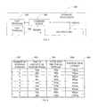
- the test program 250 in one examplemay initiate one million (M) random read commands using different numbers of working test threads 255 .
- Column 652 in table 650indicates the number of working test threads 255 initiating concurrent read commands.
- the second row in table 650represents two test threads 255 issuing random read commands concurrently to a SSD drive 605 in disk drives 500 and/or 600 .
- the fourth row in column 652represents four test threads 255 issuing random read commands concurrently to SSD drive 605 in disk drives 500 and/or 600 .
- Example numeric values provided in the subsequent descriptionare for illustrative purposes and are not representative of an actual test result. Actual numeric values will vary depending on the performance of SSD drive 605 and the design of storage processor 200 .
- Column 654indicates the time required to execute the 1M read commands. For example, a single test thread 255 may execute 1M random read commands in 100 seconds (secs) and two concurrent test threads 255 may execute 1M random read commands in 65 sec. The reduced time for two working threads may be attributable to the SSD drive 605 conducting parallel physical accesses to the memory devices 630 and not having to wait for each read command as previously shown in FIG. 4 .
- the times in column 654continue to decrease as additional test threads 255 are used for increasing the number of concurrent read operations serviced by the SSD drive 605 .
- SSD drive 605may not be able to execute the 1M read commands in less than 30 secs, regardless of the number of working threads 255 .
- read commandsmay stall in drive queue 620 while other read commands access memory devices 630 . Accordingly, sending more than seven concurrent read commands to SSD drive 605 may not reduce the time required to complete the 1M random read commands.
- Column 656indicates the total wait time for the threads 255 .
- One working test thread 255may wait 100 microseconds (usec) to receive back data for one read command.
- the storage processor overhead times 21 and 22 as shown in FIGS. 3 and 4may each be 25 usec and the physical disk access time 30 in SSD drive 605 may be 50 usec.
- the total wait time for two concurrent working threads 255is longer than the total wait time for one working thread 255 .
- the total wait time for two threads for 1M random read commandsis 150 sec as shown in the second row of column 656 and the average read latency for each thread is 150 usec as indicated in the second row of column 658 .
- additional disk access delaysmay be experienced by the test threads 255 after some number of concurrent read commands.
- SSD drive 605may experience stalls 60 and 62 due to command queuing delays 31 and data transport delays 33 , respectively. These additional delays are in additional to the storage processor overhead 21 and 22 shown in FIG. 5 .
- test threads 255may experience additional disk access delays/stalling after four concurrent reads. Up until four working threads, each additional working thread 255 may generally only add 50 usec to the total wait time in column 658 . For example, each additional working thread 255 may only increase latency due to the storage processor overhead 21 and 22 .
- the total additional wait timeincreases by 83 usecs, compared with the previous 50 usec increase associated with storage processor overhead 21 and 22 .
- the time to execute 1M random read commands with five working threads 255is reduced from 40 secs to 35 secs in column 654 .
- the total wait time for the five threadsincreases to 333 secs in column 656 . Therefore, the average read latency as indicated in column 658 is 333 usec indicting that each thread would likely wait on average of 333 usec to receive back data from SSD drive 605 .
- FIG. 9is a graph showing a performance curve or performance pattern for the data monitored in table 650 of FIG. 8 .
- the horizontal axisindicates a number of concurrent read commands 110 submitted to the SSD drive 605 and the vertical axis indicates an average read latency in microseconds (usec) per read command.
- the horizontal axiscorresponds with the number of active working threads shown in column 652 in FIG. 8 and the vertical axis corresponds with the average read latency as shown in column 658 in FIG. 8 .
- the performance curve 700identifies the characteristics of a particular SSD drive 605 for different numbers of concurrent read commands.
- the shape of curve 700may vary depending on the size, speed, number of memory devices 630 , the structure of the drive controller 610 , how data is striped across the memory devices 630 , the size of the drive queue 620 , data transport times to and from the SSD drive, overhead processing times, or the like, or any combination thereof.
- Section 701 of curve 700corresponds with the average read latency for 1-4 concurrent read commands. As explained above in FIG. 8 , four read commands may be conducted in parallel with relatively little additional read latency. Each additional concurrent read command in section 701 may only increase the average read latency by some amount attributable to storage processor overhead 21 and 22 as shown in FIGS. 3 and 4 .
- Section 702 of curve 700identifies the average read latency for 4-7 concurrent read operations.
- Section 702has a steeper slope than section 701 that may be attributable to the additional stalling 60 and 62 in FIG. 6 when the SSD drive 605 services additional concurrent read commands.
- additional stalling 60may be due to the drive controller 610 waiting to access memory devices 630 currently servicing other storage commands.
- Other stalling 62may happen while the drive controller 610 in SSD drive 605 waits to send data back to the storage processor 200 over connection 310 or connection 12 B.
- Section 703 of curve 700identifies the average read latency for 8-10 concurrent read commands
- Section 703has a steeper slope than section 701 or 702 indicating further read latency in the SSD drive 605 caused by additional concurrent read commands.
- section 701 of curve 700There is substantially little queuing penalty in section 701 of curve 700 since most read commands may be processed quickly and the only added latency is from storage processor overhead.
- the SSD drive 605may be under utilized in section 701 since additional concurrent operations could increase the total number of storage commands that could be performed in a particular time period.
- Section 702indicates some latency penalty for additional concurrent queuing in the SSD drive 605 .
- the additional queuingmay also improve overall utilization of the SSD drive 605 since more storage commands may be completed within a given period of time.
- Section 703indicates queuing more than seven read commands provides no improvement in overall performance of the SSD drive 605 and also substantially increases the average read latency. For example, every additional concurrent read command in section 703 is likely to collide with other read commands currently being serviced by memory devices 630 . Further, every additional concurrent read command is also likely to stall while data for other read commands is transmitted back to the storage processor 200 . Thus, operating in section 703 may reduce overall performance of SSD drive 605 since the read latency may be substantially increased without any additional increase the number of executed storage operations.
- good performance of SSD drive 605may be associated with location 704 in curve 700 where section 701 ends and section 702 starts.
- Location 704may indicate a level of queuing that provides good utilization of SSD drive 605 without adding unnecessary read latency due to command queuing delay 31 or data transport delay 33 .
- a desired number of concurrent read commands for SSD drive 605may be in some general area around location 704 .
- the area around location 704is associated with adequate utilization of SSD drive 605 while also maintaining a relatively low read latency.
- the desired operating location in curve 700may vary depending on the slope of sections 701 , 702 , and 703 .
- less slope in section 702may indicate less read latency delay due to collisions in SSD drive 605 .
- the target number of concurrent read commandsmay be selected higher up in section 702 .
- the target number of concurrent read commandsmay be selected in a upper location of section 701 or a lower location in section 702 .
- FIG. 10depicts one example of how the performance of SSD drive 605 may change over time.
- the SSD drive 605may use an indirection table to access memory devices 630 . Over time portions of data associated with storage access commands may be spread over a larger number of the memory devices 630 . The disjointed data may either reduce the number of concurrent read commands performed by SSD drive 605 or may increase the amount of time for the SSD drive 605 to reassemble the data. Thus, read latency for SSD device 605 may vary based on the state of the indirection table, how data is spread across the memory devices 630 , and the amount of time required to reassemble the data spread over the different memory devices 630 .
- FIG. 10shows one example of how SSD drive 605 changes from performance curve 700 to performance curve 710 .
- Performance curve 710may be derived by storage processor 200 at some later time in a similar manner as described above in FIGS. 7 and 8 .
- a first section 712 of performance curve 710is associated with 1-3 concurrent read commands and has a steeper slope than section 701 of curve 700 .
- a second section 714 of curve 710is associated with more than three concurrent read commands and has a steeper slope than section 702 of curve 700 .
- Performance curve 710shows that more than three concurrent read commands substantially increase the average read latency of SSD drive 605 .
- SSD drive 605may not be able to efficiently service more than three concurrent read commands.
- Storage processor 200may dynamically adjust the number of storage commands queued in SSD drive 605 to correspond with the updated performance curve 710 . For example, storage processor 200 may change from queuing no more than five read commands in the SSD drive 605 to queuing no more than three read commands in SSD drive 605 . Basing drive queuing on performance curves 700 and 710 maintains high drive utilization and low read latency even when the SSD drive 605 changes operating characteristics.
- FIG. 11shows an example of how the performance curves for the SSD drives 605 may be used by storage processor 200 .
- the performance curves 700 and 710may serve as a predictor of SSD drive performance for different numbers of concurrent storage accesses.
- storage processor 200may measure the read performance for a particular SSD drive 605 .
- storage processor 200may operate the test routine described above in FIGS. 7 and 8 to determine the read latency for one or more concurrent read commands.
- storage processor 200may forward one or more read commands 110 from initiator 100 to SSD drive 605 and record the read latencies for SSD drive 605 .
- storage processor 200determines if the measured read latency is within a write rotation limit.
- the write rotation limitmay be based on the performance curve 700 in FIG. 10 and in one example, may be identified as 300 usecs.
- SSD drive 605is maintained in a write rotation in operation 914 .
- the storage processor 200will continue to write data to SSD drive 605 and read data from the SSD drive 605 .
- Storage processor 200 in operation 906may determines if SSD drive 605 is performing within a second use limit, when SSD drive 605 is not operating within the write rotation limit in operation 904 . For example, based on performance curve 700 or 710 in FIG. 10 , storage processor 2000 may identify a use limit of 900 usecs. The use limit may represent a condition where SSD drive 605 can no longer be used due to an unacceptably long average read latency.
- storage processor 200may remove the SSD drive 605 from write rotation in operation 912 but continue to read data from the SSD drive 605 . For example, to stop additional fragmentation of data across the different memory devices 630 , storage processor 200 may stop writing new data into SSD drive 605 .
- storage processor 200may schedule SSD drive 605 for a secure erase in operation 910 .
- the indirection table in SSD drive 605may be invalidated effectively erasing all of the data.
- the SSD drive 605is then removed from write rotation in operation 912 .
- storage processor 200may start writing data back into the SSD drive 605 and return to operation 902 .
- the SSD drive 605is located in disk drives 600 and used as a cache or tiering media.
- Storage processor 200may erase the SSD drive 605 and reload new data from disk drives 500 in target 400 .
- SSD drive 605is located in disk drives 500 of target 400 .
- Storage processor 200may read data from the SSD drive 605 in disk drives 500 , schedule the secure erase operation 910 , and then rewrite the reassemble data back into the SSD drive 605 of disk drives 500 .
- FIG. 12depicts an example of storage processor 200 in more detail.
- Command queue 300 , threads 250 , and a command scheduler 310comprise logic circuitry, software, buffers, memory, registers, or the like, or any combination thereof used by the storage processor 200 for performing the operations described below.
- Command queue 300buffers read and/or write commands 302 received from initiator 100 .
- command queue 300contains read commands 302 A- 302 N.
- Read commands 302may include an identifier associated with the initiator 100 and an address associated with data contained in the disk drives 600 and/or 500 .
- threads 250may be controlled and parallelized via operating system software that operates command scheduler software 310 .
- Multi-threaded processors and multi-threaded operating systemsare known to those skilled in the art and are therefore not described in further detail.
- Command scheduler 310may control which read commands 302 are assigned to threads 250 , when read commands 302 are assigned to the threads 250 , and in what order read commands 302 are assigned to threads 250 . Threads 250 use the address associated with the assigned read commands 302 to identify the SSD drive 605 for servicing the read command.
- Command scheduler 310may use any variety of schemes for assigning read commands 302 to threads 250 .
- command scheduler 310may issue the read commands to the threads 250 on a round robin basis where each read command 302 in command queue 300 is assigned to a next one of threads 250 .
- the command scheduler 310may use a scheme that prevents head of line blocking. For example, thread 250 A may currently be servicing four currently pending read commands 302 all directed to the same SSD drive 605 A in FIG. 2 .
- a next read command 302 A in command queue 300may be directed to the same SSD drive 605 A.
- Command scheduler 310may defer assigning the read command 302 A to one of the threads 250 and assign the next read command 302 B to a next thread 250 B.
- read command 302 Bis directed to a different SSD drive 605 B not currently servicing any pending read commands 302 .
- Thread 250 Bcan then immediately service read command 302 B with SSD drive 605 B instead of waiting for thread 250 A to finish the four currently pending read commands on SSD drive 605 A.
- Command scheduler 310may monitor threads 250 to determine their current workload and monitor the different SSD drives 605 to determine their current workload. Command scheduler 310 may then assign the read commands 302 to threads 250 according to the monitored workloads and predicted read latency.
- FIG. 13depicts an example of a thread monitor 320 operated by command scheduler 310 and FIG. 14 depicts an example of a device monitor 330 operated by command scheduler 310 .
- Thread monitor 320includes a device map 325 that identifies SSD drives 605 currently used by a particular thread 250 for servicing read commands 302 .
- Device map 325may be a bit map or other data structure that identifies the SSD drives 605 .
- thread monitor 320may identify each SSD drive 605 accessed by a particular thread 250 A and list the identified SSD drives 605 in the device map 325 associated with that particular thread 250 A.
- a thread map 335 in device monitor 330may be a bit map or other data structure that identifies the threads 250 accessing a particular SSD drive 605 .
- Device monitor 330may identify each thread 302 accessing a particular SSD drive 605 and list the identified threads in thread map 335 .
- Device map 325 and thread map 335may be updated whenever a read command 302 is assigned to a particular thread 250 .
- command scheduler 310may assign a particular read command 302 to a particular thread 250 .
- the thread monitor 320may identify the SSD drive 605 associated with the read command address and update the device map 325 for the assigned thread 250 with the identified SSD drive 605 .
- Device monitor 330may similarly update the thread map 335 for the identified SSD drive 605 with the assigned thread 250 .
- thread monitor 320may remove the particular SSD drive 605 from the device map 325 for the associated thread 250 and the device monitor 330 may remove the particular thread 250 from the thread map 335 for the associated SSD drive 605 .
- Thread monitor 320may also track a thread debt value 327 corresponding to an amount of processing debt/delay for the associated thread 250 and device monitor 330 may also track a device debt value 337 corresponding to an amount of processing debt/delay for the associated SSD drive 605 . Examples of how the thread debt value 327 and device debt value 337 are derived for a particular thread 250 and SSD drive 605 , respectively, are explained in more detail below.
- FIG. 15depicts an example of a process for operating a command scheduler.
- the command schedulermay try and assign as many read commands 302 as possible to threads 250 as long as the predicted latency for the assigned read commands is relatively low.
- the command schedulermay try and prevent assigning read commands 302 that would likely stall subsequent read commands 302 based on the thread debt value 327 for the candidate thread 250 or the device debt value 337 for the associated SSD drive 605 .
- the command scheduler in operation 902receives a read command 302 from command queue 300 and identifies the device debt value 337 for the associated SSD drive 605 in operation 904 .
- the command scheduleridentifies the SSD drive 605 associated with the address in the read command 302 and identifies the device debt value 337 associated with the identified SSD drive 605 .
- the device debt value 337is compared with a limit value in operation 904 .
- the limit valuemay be identified based on the dynamically changing performance curves 700 and/or 710 associated with the identified SSD drive 605 .
- the command schedulermay be configured to identify the location 704 in FIG. 10 where section 701 of curve 700 ends and section 702 begins.
- the limit value in operation 904may be selected as a certain number of concurrent reads around location 704 .
- location 704may be associated with four concurrent read commands.
- the command schedulermay be configured to set the limit value in operation 904 to two concurrent reads above location 704 , e.g., six concurrent reads.
- the performance of the SSD drivemay change over time from performance curve 700 to performance curve 710 .
- Location 715 in curve 710corresponds with three concurrent read commands and identifies the beginning of section 714 .
- Section 714 of curve 710has a high slope and an associated high average read latency.
- the command schedulermay not issue more than three concurrent read commands when the SSD drive 605 is operating according to performance curve 710 .
- the command schedulermay be configured to change the limit value used in operation 904 to correspond with the dynamically changing performance curve for the SSD drive 605 .
- the command schedulermay change the limit value in operation 904 from the six concurrent reads corresponding with curve 700 to the three concurrent reads corresponding with curve 710 .
- the command schedulermay defer the read command in operation 920 .
- the SSD drive 605 associated with the read command 302may currently have seven pending read commands 302 and the device debt limit may be six.
- the command schedulermay skip over the read command 302 and process a next read command 302 in command queue 300 in operation 902 .
- the deferred read command 302may be reevaluated in a round-robin manner after other read commands 302 in command queue 300 are processed.
- Other schemescan also be used, such as reevaluating the deferred read command after processing a certain number of other read commands, periodically reevaluating the deferred read command after a given time period, reevaluating the deferred read command when the device debt value 337 associated with the read command falls below a particular level, or the like, or any combination thereof.
- the command schedulermay assign the read command to a thread 250 after a certain time period has passed, regardless of the associated device debt value.
- the command schedulermay issue the read command 302 to a thread 250 when the device debt value 337 is below the limit value in operation 904 .
- the command scheduler in operation 906may select a candidate thread based on the thread map 335 for the SSD drive 605 associated with the read command 302 .
- the command schedulermay identify one of threads 250 that is not currently accessing the associated SSD drive 605 .
- command schedulermay identify one of the threads 250 not currently listed in the thread map 335 for the associated SSD drive 605 .
- the candidate threadmay need to be selected in operation 906 from one of the threads 250 already accessing the SSD drive.
- the command schedulermay select one of the candidate threads 250 with a lowest thread debt value 327 and in operation 910 may issue the read command 302 to the selected thread 250 .
- the cost of assigning the read command 302 to a thread 250may be proportional to the expected concurrency that that thread might encounter.
- four read commands 302may be assigned to a thread 250 and each of the four read commands 302 may be associated with a different SSD drive 605 that is currently processing only one other read command.
- the thread 250is likely to complete the four read commands 302 quickly since there will likely be little stalling due to collisions with other read commands.
- four read commands 302may be assigned to a thread 250 and each of the four read commands 302 may be associated with a different SSD drive 605 currently processing four other read commands.
- the thread 250is likely to take substantially longer to complete the four read commands 320 due to the higher number of collisions and read latency on each of the four SSD drives 605 .
- the thread monitormay take into account the number of pending read commands on the associated SSD drives 605 in operation 912 by adding the device debt to the thread debt.
- the four associated SSD drivesonly have one other pending read command 302 .
- the thread debt value 327 for the assigned thread 250may be incremented by four to account for four SSD drives each with a current device debt value 337 of one.
- each of the four SSD driveshas four pending read commands 302 .
- the thread debt value 327 for the assigned thread 250may be increased in operation 912 by sixteen to account for the four SSD drives each having a device debt value 337 of four.
- An example of how to increase the thread debt value 327 in operation 912is described in more detail in FIGS. 16 and 17 .
- the device monitormay increase the device debt value 337 for the SSD drive 605 associated with the issued read command. For example, the device monitor may increment the device debt value 337 for the associated SSD drive by one.
- An example, of how to increase the device debt value 337 in operation 914is also described in more detail in FIGS. 16 and 17 .
- the device debt value 337may also be scaled according to deviations between the predicted latency of the SSD drive 605 and the measured latency of the SSD drive 605 .
- a last completed read command 302 for a particular SSD drivemay have had a higher latency than the latency predicted in performance curve 700 in FIG. 10 .
- the last read command 302 completed for a SSD drive 605may have been the fifth concurrent read command for that particular SSD drive 605 .
- Performance curve 700may have predicted a read latency of 333 usec for the read command. However, the actual read latency may have been 500 usec.
- the command schedulermay further increase the device debt value 337 to correspond with the additional read latency likely to be associated with the SSD drive 605 .
- This directed scaling of the device debt value 337may provide immediate storage access optimization for the SSD drive when not operating according to the predicted performance curve 700 .
- the additional scaling of the device debt value 337is likely to immediately reduce the number of concurrent reads assigned to the underperforming SSD drive.
- the command schedulermonitors for completion of the read command 302 in operation 916 .
- the command schedulermay detect a signal from SSD drive 605 or detect when data associated with a particular read command 302 is received back in a data queue (not shown) in the storage processor 200 .
- the device debt value 337 associated with the SSD drive 605 providing the data for the completed read command and the thread debt value 327 for the thread 250 servicing the completed read commandare both reduced.
- the device debt value 337 and/or thread debt value 327may be reduced in a same manner as previously increased.
- the device debt value 337 for the SSD drive providing data for the read commandmay be decremented by one and the thread debt value for the thread 250 servicing the read command may be reduced based on the device debt value of the SSD drive.
- the command schedulermay also scale the reduction of the device debt value 337 and/or thread debt value 327 according to discrepancies between the actual measured read latency and the predicted read latency for the completed read command. For example, the thread debt value 327 and/or device debt value 337 may be reduced by a lesser amount when the measured read latency is greater than that predicted read latency associated with performance curve 700 .
- FIGS. 16 and 17depict the two examples described above for increasing thread debt value 327 and device debt value 337 .
- four read commands 1-4are received in command queue 300 and are directed to four different SSD drives A-D, respectively.
- Command scheduler 310assigns all four read commands 1-4 to a thread M that has a current thread debt value of zero.
- Each of the four SSD drives A-Dcurrently has a device debt value of one that in one example may indicate each of the four SSD drives A-D is currently processing one read command.
- Thread monitor 320increases the thread debt value 327 for thread M to four reflecting the device debt value 337 of one for each of four memory devices A-D.
- Device monitor 330increases each of the device debt values 337 from one to two for each of the four SSD drives A-D indicating each now has two pending read commands.
- command queue 300four read commands 1-4 are received in command queue 300 and are directed to four different SSD drives A-D, respectively.
- Command scheduler 310assigns all four read commands 1-4 to thread M that has a current thread debt value 327 of zero.
- Each of the four SSD drives A-Dcurrently has a device debt value 337 of four that in one example may indicate each of the four SSD drives A-D is currently servicing four read commands.
- Thread monitor 320increases the thread debt value 327 for thread M to sixteen to reflect the device debt value of four for each of four memory devices A-D.
- Device monitor 330increases of the device debt values 337 from four to five indicating each of the four SSD drives A-D now has five pending read commands.
- thread debt values 327 and device debt values 337may be reduced in a same manner when the corresponding read commands are completed.
- thread monitor 320may reduce the thread debt value for thread M by one when each of the read commands 1-4 is completed.
- the thread monitor 320may reduce the thread debt value for thread M by four when one of the read commands 1-4 in FIG. 17 is completed.
- command scheduler 310schedules the read commands 302 in an optimal operating range of the SSD drives that adequately utilizes the capacity of the SSD drives without unnecessarily increasing latency for individual storage access commands
- the commandsare described as various interconnected functional blocks or distinct software modules. This is not necessary, however, and there may be cases where these functional blocks or modules are equivalently aggregated into a single logic device, program or command with unclear boundaries.
- the functional blocks and software modules or features of the flexible interfacecan be implemented by themselves, or in combination with other commands in either hardware or software.
- digital computing systemcan mean any system that includes at least one digital processor and associated memory, wherein the digital processor can execute instructions or “code” stored in that memory. (The memory may store data as well.)
- a digital processorincludes but is not limited to a microprocessor, multi-core processor, Digital Signal Processor (DSP), Graphics Processing Unit (GPU), processor array, network processor, etc.
- DSPDigital Signal Processor
- GPUGraphics Processing Unit
- a digital processor(or many of them) may be embedded into an integrated circuit. In other arrangements, one or more processors may be deployed on a circuit board (motherboard, daughter board, rack blade, etc.).
- Embodiments of the present disclosuremay be variously implemented in a variety of systems such as those just mentioned and others that may be developed in the future. In a presently preferred embodiment, the disclosed methods may be implemented in software stored in memory, further defined below.
- Digital memorymay be integrated together with a processor, for example Random Access Memory (RAM) or FLASH memory embedded in an integrated circuit Central Processing Unit (CPU), network processor or the like.
- the memorycomprises a physically separate device, such as an disk drive, storage array, or portable FLASH device.
- the memorybecomes “associated” with the digital processor when the two are operatively coupled together, or in communication with each other, for example by an I/O port, network connection, etc. such that the processor can read a file stored on the memory.
- Associated memorymay be “read only” by design (ROM) or by virtue of permission settings, or not.
- Other examplesinclude but are not limited to WORM, EPROM, EEPROM, FLASH, etc.
- Computer-readable storage mediumincludes all of the foregoing types of memory, as well as new technologies that may arise in the future, as long as they are capable of storing digital information in the nature of a computer program or other data, at least temporarily, in such a manner that the stored information can be “read” by an appropriate digital processor.
- computer-readableis not intended to limit the phrase to the historical usage of “computer” to imply a complete mainframe, mini-computer, desktop or even laptop computer. Rather, the term refers to a storage medium readable by a digital processor or any digital computing system as broadly defined above.
- Such mediamay be any available media that is locally and/or remotely accessible by a computer or processor, and it includes both volatile and non-volatile media, removable and non-removable media, embedded or discrete.
Landscapes
- Engineering & Computer Science (AREA)
- Theoretical Computer Science (AREA)
- Human Computer Interaction (AREA)
- Physics & Mathematics (AREA)
- General Engineering & Computer Science (AREA)
- General Physics & Mathematics (AREA)
- Debugging And Monitoring (AREA)
Abstract
Description
Claims (21)
Priority Applications (1)
| Application Number | Priority Date | Filing Date | Title |
|---|---|---|---|
| US13/019,617US8972689B1 (en) | 2011-02-02 | 2011-02-02 | Apparatus, method and system for using real-time performance feedback for modeling and improving access to solid state media |
Applications Claiming Priority (1)
| Application Number | Priority Date | Filing Date | Title |
|---|---|---|---|
| US13/019,617US8972689B1 (en) | 2011-02-02 | 2011-02-02 | Apparatus, method and system for using real-time performance feedback for modeling and improving access to solid state media |
Publications (1)
| Publication Number | Publication Date |
|---|---|
| US8972689B1true US8972689B1 (en) | 2015-03-03 |
Family
ID=52575222
Family Applications (1)
| Application Number | Title | Priority Date | Filing Date |
|---|---|---|---|
| US13/019,617Active2033-10-05US8972689B1 (en) | 2011-02-02 | 2011-02-02 | Apparatus, method and system for using real-time performance feedback for modeling and improving access to solid state media |
Country Status (1)
| Country | Link |
|---|---|
| US (1) | US8972689B1 (en) |
Cited By (8)
| Publication number | Priority date | Publication date | Assignee | Title |
|---|---|---|---|---|
| US20150220274A1 (en)* | 2014-02-05 | 2015-08-06 | Quanta Storage Inc. | Reading Method of Solid State Disk |
| WO2016160216A1 (en)* | 2015-03-27 | 2016-10-06 | Intel Corporation | Measurement and reporting of the latency of input and output operations by a solid state drive to a host |
| US10019174B2 (en) | 2015-10-27 | 2018-07-10 | Sandisk Technologies Llc | Read operation delay |
| US10157123B1 (en)* | 2013-07-31 | 2018-12-18 | Juniper Networks, Inc. | Methods and apparatus for a scheduler for memory access |
| US10289304B2 (en)* | 2013-11-06 | 2019-05-14 | International Business Machines Corporation | Physical address management in solid state memory by tracking pending reads therefrom |
| US10853283B1 (en) | 2019-06-19 | 2020-12-01 | Intel Corporation | Integrated circuits for generating input/output latency performance metrics using real-time clock (RTC) read measurement module |
| US11418361B2 (en)* | 2019-07-25 | 2022-08-16 | Samsung Electronics Co., Ltd. | Master device, system and method of controlling the same |
| US20230042551A1 (en)* | 2021-08-03 | 2023-02-09 | Samsung Electronics Co., Ltd. | Systems, methods, and apparatus for the management of device local memory |
Citations (80)
| Publication number | Priority date | Publication date | Assignee | Title |
|---|---|---|---|---|
| US5861893A (en)* | 1997-05-27 | 1999-01-19 | Intel Corporation | System and method for graphics data concurrency and coherency |
| US5954796A (en) | 1997-02-11 | 1999-09-21 | Compaq Computer Corporation | System and method for automatically and dynamically changing an address associated with a device disposed in a fire channel environment |
| US6041366A (en) | 1998-02-02 | 2000-03-21 | International Business Machines Corporation | System and method for dynamic specification of input/output attributes |
| US20020035655A1 (en) | 2000-09-15 | 2002-03-21 | Dawn Finn | Method of checking for and recovering from underruns and overrun slips when writing to circular buffers in dynamic bandwidth circuit emulation services |
| US6401147B1 (en) | 1999-05-24 | 2002-06-04 | Advanced Micro Devices, Inc. | Split-queue architecture with a first queue area and a second queue area and queue overflow area having a trickle mode and an overflow mode based on prescribed threshold values |
| US20020175998A1 (en) | 2000-05-31 | 2002-11-28 | Hoang Khoi Nhu | Data-on-demand digital broadcast system utilizing prefetch data transmission |
| US20020194434A1 (en) | 2001-06-13 | 2002-12-19 | Toshiyasu Kurasugi | Method of prefetching reference objects using wieght values of referrer objects |
| US20030012204A1 (en) | 2001-07-11 | 2003-01-16 | Sancastle Technologies, Ltd | Extension of fibre channel addressing |
| US20030167327A1 (en) | 2001-10-05 | 2003-09-04 | Baldwin Duane Mark | Storage area network methods and apparatus for topology rendering |
| US20030177168A1 (en) | 2001-10-05 | 2003-09-18 | Heitman Allen Robert | Storage area network methods and apparatus for validating data from multiple sources |
| US6636982B1 (en) | 2000-03-03 | 2003-10-21 | International Business Machines Corporation | Apparatus and method for detecting the reset of a node in a cluster computer system |
| US20030210248A1 (en) | 2002-05-08 | 2003-11-13 | Wyatt David A. | Method and system for optimally sharing memory between a host processor and graphics processor |
| US6678795B1 (en) | 2000-08-15 | 2004-01-13 | International Business Machines Corporation | Method and apparatus for memory prefetching based on intra-page usage history |
| US6721870B1 (en) | 2001-06-12 | 2004-04-13 | Emc Corporation | Prefetch algorithm for short sequences |
| US6742084B1 (en) | 1998-05-15 | 2004-05-25 | Storage Technology Corporation | Caching method for selecting data blocks for removal from cache based on recall probability and size |
| US20040128363A1 (en) | 2001-03-30 | 2004-07-01 | Hitachi, Ltd. | Remote copy with path selection and prioritization |
| US20040146046A1 (en) | 2003-01-16 | 2004-07-29 | Ntt Docomo, Inc. | Path control device and path control method |
| US6789171B2 (en) | 2002-05-31 | 2004-09-07 | Veritas Operating Corporation | Computer system implementing a multi-threaded stride prediction read ahead algorithm |
| US20040186945A1 (en) | 2003-03-21 | 2004-09-23 | Jeter Robert E. | System and method for dynamic mirror-bank addressing |
| US6810470B1 (en) | 2000-08-14 | 2004-10-26 | Ati Technologies, Inc. | Memory request interlock |
| US20040215923A1 (en) | 2003-04-22 | 2004-10-28 | Royer Robert J. | Optimally mapping a memory device |
| US20050025075A1 (en) | 2001-12-26 | 2005-02-03 | Cisco Technology, Inc. | Fibre channel switch that enables end devices in different fabrics to communicate with one another while retaining their unique fibre channel domain_IDs |
| US20050195736A1 (en) | 2004-03-08 | 2005-09-08 | Yasuhiro Matsuda | Information processing apparatus and method of controlling the information processing apparatus |
| US20060005074A1 (en) | 1993-04-23 | 2006-01-05 | Moshe Yanai | Remote data mirroring |
| US20060034302A1 (en) | 2004-07-19 | 2006-02-16 | David Peterson | Inter-fabric routing |
| US20060053263A1 (en) | 2004-04-30 | 2006-03-09 | Anand Prahlad | Systems and methods for generating a storage-related metric |
| US7017084B2 (en) | 2001-09-07 | 2006-03-21 | Network Appliance Inc. | Tracing method and apparatus for distributed environments |
| US20060075191A1 (en) | 2001-09-28 | 2006-04-06 | Emc Corporation | Pooling and provisioning storage resources in a storage network |
| US20060112232A1 (en) | 2004-08-09 | 2006-05-25 | Xiv Ltd. | Method and apparatus for managing a cache memory in a mass-storage system |
| US7089370B2 (en) | 2003-09-30 | 2006-08-08 | International Business Machines Corporation | Apparatus and method for pre-fetching page data using segment table data |
| US7110359B1 (en) | 2001-03-05 | 2006-09-19 | Advanced Micro Devices, Inc. | System and method for dynamically updating weights of weighted round robin in output queues |
| US20060212524A1 (en) | 2005-03-15 | 2006-09-21 | Riverbed Technology | Rules-based transaction prefetching using connection end-point proxies |
| US20060218389A1 (en) | 2005-03-22 | 2006-09-28 | Microsoft Corporation | System and method for identity decisions and invalidation |
| US20060277329A1 (en) | 2005-06-07 | 2006-12-07 | Paulson Christopher D | Method for reducing latency |
| US20070050548A1 (en) | 2005-08-26 | 2007-03-01 | Naveen Bali | Dynamic optimization of cache memory |
| US20070079105A1 (en) | 2005-10-05 | 2007-04-05 | Thompson Mark J | Data misalignment detection and correction in a computer system utilizing a mass storage subsystem |
| US20070118710A1 (en) | 2005-11-18 | 2007-05-24 | Hiroshi Yamakawa | Storage system and data migration method |
| US20070124407A1 (en) | 2005-11-29 | 2007-05-31 | Lsi Logic Corporation | Systems and method for simple scale-out storage clusters |
| US20070192444A1 (en) | 2002-09-16 | 2007-08-16 | Emmanuel Ackaouy | Apparatus and method for a proxy cache |
| US20070233700A1 (en) | 2006-03-30 | 2007-10-04 | Kazusa Tomonaga | Storage cluster system, data processing method, and program |
| US20070283086A1 (en) | 2006-06-06 | 2007-12-06 | Seagate Technology Llc | Write caching random data and sequential data simultaneously |
| US20080028162A1 (en) | 2006-07-26 | 2008-01-31 | Thompson Mark J | Automatic data block misalignment detection and correction in a computer system utilizing a hard disk subsystem |
| US20080098173A1 (en) | 2006-10-20 | 2008-04-24 | Lakshminarayanan Chidambaran | Consistent client-side cache |
| US20080104363A1 (en) | 2006-10-26 | 2008-05-01 | Ashok Raj | I/O translation lookaside buffer performance |
| US20080162864A1 (en) | 2006-12-27 | 2008-07-03 | Suresh Sugumar | Guest to host address translation for devices to access memory in a partitioned system |
| US20080215834A1 (en) | 2007-03-01 | 2008-09-04 | Douglas Dumitru | Fast block device and methodology |
| US20080215827A1 (en) | 2005-11-22 | 2008-09-04 | International Business Machines Corporation | Selecting storage clusters to use to access storage |
| US20080250195A1 (en) | 2000-01-06 | 2008-10-09 | Super Talent Electronics Inc. | Multi-Operation Write Aggregator Using a Page Buffer and a Scratch Flash Block in Each of Multiple Channels of a Large Array of Flash Memory to Reduce Block Wear |
| US20080320269A1 (en) | 2007-06-21 | 2008-12-25 | John Richard Houlihan | Method and apparatus for ranking of target server partitions for virtual server mobility operations |
| US20090006725A1 (en) | 2006-12-15 | 2009-01-01 | Takafumi Ito | Memory device |
| US20090006745A1 (en) | 2007-06-28 | 2009-01-01 | Cavallo Joseph S | Accessing snapshot data image of a data mirroring volume |
| US20090034377A1 (en) | 2007-04-27 | 2009-02-05 | English Robert M | System and method for efficient updates of sequential block storage |
| US20090110000A1 (en) | 2007-10-31 | 2009-04-30 | Morten Brorup | Apparatus and a method for distributing bandwidth |
| US20090119481A1 (en)* | 2005-11-29 | 2009-05-07 | Xmtt Inc. | Computer memory architecture for hybrid serial and parallel computing systems |
| US20090150576A1 (en)* | 2007-12-06 | 2009-06-11 | Joaquin Madruga | Dynamic logical data channel assignment using channel bitmap |
| US20090157994A1 (en)* | 2006-05-02 | 2009-06-18 | Hampel Craig E | Memory module with reduced access granularity |
| US20090240873A1 (en) | 2003-12-02 | 2009-09-24 | Super Talent Electronics Inc. | Multi-Level Striping and Truncation Channel-Equalization for Flash-Memory System |
| US20090259800A1 (en) | 2008-04-15 | 2009-10-15 | Adtron, Inc. | Flash management using sequential techniques |
| US7606944B2 (en)* | 2007-05-10 | 2009-10-20 | Dot Hill Systems Corporation | Dynamic input/output optimization within a storage controller |
| US20090262741A1 (en) | 2000-06-23 | 2009-10-22 | Jungck Peder J | Transparent Provisioning of Services Over a Network |
| US20090276588A1 (en) | 2008-04-30 | 2009-11-05 | Atsushi Murase | Free space utilization in tiered storage systems |
| US20090307388A1 (en) | 2008-06-10 | 2009-12-10 | Yves Constantin Tchapda | Methods of providing access to i/o devices |
| US20100011154A1 (en) | 2008-07-08 | 2010-01-14 | Phison Electronics Corp. | Data accessing method for flash memory and storage system and controller using the same |
| US20100030809A1 (en) | 2008-07-31 | 2010-02-04 | Microsoft Corporation | Maintaining large random sample with semi-random append-only operations |
| US20100080237A1 (en) | 2008-09-30 | 2010-04-01 | Gridlron Systems, Inc. | Fibre channel proxy |
| US20100088469A1 (en) | 2008-10-08 | 2010-04-08 | Hitachi, Ltd. | Storage system |
| US20100115206A1 (en) | 2008-11-04 | 2010-05-06 | Gridlron Systems, Inc. | Storage device prefetch system using directed graph clusters |
| US20100115211A1 (en) | 2008-11-04 | 2010-05-06 | Gridlron Systems, Inc. | Behavioral monitoring of storage access patterns |
| US20100122020A1 (en) | 2008-11-13 | 2010-05-13 | Gridlron Systems, Inc. | Dynamic performance virtualization for disk access |
| US20100125857A1 (en) | 2008-11-17 | 2010-05-20 | Gridlron Systems, Inc. | Cluster control protocol |
| US20100169544A1 (en) | 2008-12-31 | 2010-07-01 | Eom Young-Ik | Methods for distributing log block associativity for real-time system and flash memory devices performing the same |
| US20100174939A1 (en) | 2007-06-05 | 2010-07-08 | Vladimir Vexler | Devices for providing distributable middleware data proxy between application servers and database servers |
| US7856533B2 (en) | 2007-11-01 | 2010-12-21 | International Business Machines Corporation | Probabilistic method for performing memory prefetching |
| US7870351B2 (en) | 2007-11-15 | 2011-01-11 | Micron Technology, Inc. | System, apparatus, and method for modifying the order of memory accesses |
| US7873619B1 (en) | 2008-03-31 | 2011-01-18 | Emc Corporation | Managing metadata |
| US20110047347A1 (en) | 2009-08-19 | 2011-02-24 | Seagate Technology Llc | Mapping alignment |
| US7975108B1 (en) | 2004-03-25 | 2011-07-05 | Brian Holscher | Request tracking data prefetcher apparatus |
| US8010485B1 (en) | 2005-10-20 | 2011-08-30 | American Megatrends, Inc. | Background movement of data between nodes in a storage cluster |
| US20110258362A1 (en) | 2008-12-19 | 2011-10-20 | Mclaren Moray | Redundant data storage for uniform read latency |
| US20120198176A1 (en) | 2009-03-30 | 2012-08-02 | Via Technologies, Inc. | Prefetching of next physically sequential cache line after cache line that includes loaded page table entry |
- 2011
- 2011-02-02USUS13/019,617patent/US8972689B1/enactiveActive
Patent Citations (80)
| Publication number | Priority date | Publication date | Assignee | Title |
|---|---|---|---|---|
| US20060005074A1 (en) | 1993-04-23 | 2006-01-05 | Moshe Yanai | Remote data mirroring |
| US5954796A (en) | 1997-02-11 | 1999-09-21 | Compaq Computer Corporation | System and method for automatically and dynamically changing an address associated with a device disposed in a fire channel environment |
| US5861893A (en)* | 1997-05-27 | 1999-01-19 | Intel Corporation | System and method for graphics data concurrency and coherency |
| US6041366A (en) | 1998-02-02 | 2000-03-21 | International Business Machines Corporation | System and method for dynamic specification of input/output attributes |
| US6742084B1 (en) | 1998-05-15 | 2004-05-25 | Storage Technology Corporation | Caching method for selecting data blocks for removal from cache based on recall probability and size |
| US6401147B1 (en) | 1999-05-24 | 2002-06-04 | Advanced Micro Devices, Inc. | Split-queue architecture with a first queue area and a second queue area and queue overflow area having a trickle mode and an overflow mode based on prescribed threshold values |
| US20080250195A1 (en) | 2000-01-06 | 2008-10-09 | Super Talent Electronics Inc. | Multi-Operation Write Aggregator Using a Page Buffer and a Scratch Flash Block in Each of Multiple Channels of a Large Array of Flash Memory to Reduce Block Wear |
| US6636982B1 (en) | 2000-03-03 | 2003-10-21 | International Business Machines Corporation | Apparatus and method for detecting the reset of a node in a cluster computer system |
| US20020175998A1 (en) | 2000-05-31 | 2002-11-28 | Hoang Khoi Nhu | Data-on-demand digital broadcast system utilizing prefetch data transmission |
| US20090262741A1 (en) | 2000-06-23 | 2009-10-22 | Jungck Peder J | Transparent Provisioning of Services Over a Network |
| US6810470B1 (en) | 2000-08-14 | 2004-10-26 | Ati Technologies, Inc. | Memory request interlock |
| US6678795B1 (en) | 2000-08-15 | 2004-01-13 | International Business Machines Corporation | Method and apparatus for memory prefetching based on intra-page usage history |
| US20020035655A1 (en) | 2000-09-15 | 2002-03-21 | Dawn Finn | Method of checking for and recovering from underruns and overrun slips when writing to circular buffers in dynamic bandwidth circuit emulation services |
| US7110359B1 (en) | 2001-03-05 | 2006-09-19 | Advanced Micro Devices, Inc. | System and method for dynamically updating weights of weighted round robin in output queues |
| US20040128363A1 (en) | 2001-03-30 | 2004-07-01 | Hitachi, Ltd. | Remote copy with path selection and prioritization |
| US6721870B1 (en) | 2001-06-12 | 2004-04-13 | Emc Corporation | Prefetch algorithm for short sequences |
| US20020194434A1 (en) | 2001-06-13 | 2002-12-19 | Toshiyasu Kurasugi | Method of prefetching reference objects using wieght values of referrer objects |
| US20030012204A1 (en) | 2001-07-11 | 2003-01-16 | Sancastle Technologies, Ltd | Extension of fibre channel addressing |
| US7017084B2 (en) | 2001-09-07 | 2006-03-21 | Network Appliance Inc. | Tracing method and apparatus for distributed environments |
| US20060075191A1 (en) | 2001-09-28 | 2006-04-06 | Emc Corporation | Pooling and provisioning storage resources in a storage network |
| US20030167327A1 (en) | 2001-10-05 | 2003-09-04 | Baldwin Duane Mark | Storage area network methods and apparatus for topology rendering |
| US20030177168A1 (en) | 2001-10-05 | 2003-09-18 | Heitman Allen Robert | Storage area network methods and apparatus for validating data from multiple sources |
| US20050025075A1 (en) | 2001-12-26 | 2005-02-03 | Cisco Technology, Inc. | Fibre channel switch that enables end devices in different fabrics to communicate with one another while retaining their unique fibre channel domain_IDs |
| US20030210248A1 (en) | 2002-05-08 | 2003-11-13 | Wyatt David A. | Method and system for optimally sharing memory between a host processor and graphics processor |
| US6789171B2 (en) | 2002-05-31 | 2004-09-07 | Veritas Operating Corporation | Computer system implementing a multi-threaded stride prediction read ahead algorithm |
| US20070192444A1 (en) | 2002-09-16 | 2007-08-16 | Emmanuel Ackaouy | Apparatus and method for a proxy cache |
| US20040146046A1 (en) | 2003-01-16 | 2004-07-29 | Ntt Docomo, Inc. | Path control device and path control method |
| US20040186945A1 (en) | 2003-03-21 | 2004-09-23 | Jeter Robert E. | System and method for dynamic mirror-bank addressing |
| US20040215923A1 (en) | 2003-04-22 | 2004-10-28 | Royer Robert J. | Optimally mapping a memory device |
| US7089370B2 (en) | 2003-09-30 | 2006-08-08 | International Business Machines Corporation | Apparatus and method for pre-fetching page data using segment table data |
| US20090240873A1 (en) | 2003-12-02 | 2009-09-24 | Super Talent Electronics Inc. | Multi-Level Striping and Truncation Channel-Equalization for Flash-Memory System |
| US20050195736A1 (en) | 2004-03-08 | 2005-09-08 | Yasuhiro Matsuda | Information processing apparatus and method of controlling the information processing apparatus |
| US7975108B1 (en) | 2004-03-25 | 2011-07-05 | Brian Holscher | Request tracking data prefetcher apparatus |
| US20060053263A1 (en) | 2004-04-30 | 2006-03-09 | Anand Prahlad | Systems and methods for generating a storage-related metric |
| US20060034302A1 (en) | 2004-07-19 | 2006-02-16 | David Peterson | Inter-fabric routing |
| US20060112232A1 (en) | 2004-08-09 | 2006-05-25 | Xiv Ltd. | Method and apparatus for managing a cache memory in a mass-storage system |
| US20060212524A1 (en) | 2005-03-15 | 2006-09-21 | Riverbed Technology | Rules-based transaction prefetching using connection end-point proxies |
| US20060218389A1 (en) | 2005-03-22 | 2006-09-28 | Microsoft Corporation | System and method for identity decisions and invalidation |
| US20060277329A1 (en) | 2005-06-07 | 2006-12-07 | Paulson Christopher D | Method for reducing latency |
| US20070050548A1 (en) | 2005-08-26 | 2007-03-01 | Naveen Bali | Dynamic optimization of cache memory |
| US20070079105A1 (en) | 2005-10-05 | 2007-04-05 | Thompson Mark J | Data misalignment detection and correction in a computer system utilizing a mass storage subsystem |
| US8010485B1 (en) | 2005-10-20 | 2011-08-30 | American Megatrends, Inc. | Background movement of data between nodes in a storage cluster |
| US20070118710A1 (en) | 2005-11-18 | 2007-05-24 | Hiroshi Yamakawa | Storage system and data migration method |
| US20080215827A1 (en) | 2005-11-22 | 2008-09-04 | International Business Machines Corporation | Selecting storage clusters to use to access storage |
| US20070124407A1 (en) | 2005-11-29 | 2007-05-31 | Lsi Logic Corporation | Systems and method for simple scale-out storage clusters |
| US20090119481A1 (en)* | 2005-11-29 | 2009-05-07 | Xmtt Inc. | Computer memory architecture for hybrid serial and parallel computing systems |
| US20070233700A1 (en) | 2006-03-30 | 2007-10-04 | Kazusa Tomonaga | Storage cluster system, data processing method, and program |
| US20090157994A1 (en)* | 2006-05-02 | 2009-06-18 | Hampel Craig E | Memory module with reduced access granularity |
| US20070283086A1 (en) | 2006-06-06 | 2007-12-06 | Seagate Technology Llc | Write caching random data and sequential data simultaneously |
| US20080028162A1 (en) | 2006-07-26 | 2008-01-31 | Thompson Mark J | Automatic data block misalignment detection and correction in a computer system utilizing a hard disk subsystem |
| US20080098173A1 (en) | 2006-10-20 | 2008-04-24 | Lakshminarayanan Chidambaran | Consistent client-side cache |
| US20080104363A1 (en) | 2006-10-26 | 2008-05-01 | Ashok Raj | I/O translation lookaside buffer performance |
| US20090006725A1 (en) | 2006-12-15 | 2009-01-01 | Takafumi Ito | Memory device |
| US20080162864A1 (en) | 2006-12-27 | 2008-07-03 | Suresh Sugumar | Guest to host address translation for devices to access memory in a partitioned system |
| US20080215834A1 (en) | 2007-03-01 | 2008-09-04 | Douglas Dumitru | Fast block device and methodology |
| US20090034377A1 (en) | 2007-04-27 | 2009-02-05 | English Robert M | System and method for efficient updates of sequential block storage |
| US7606944B2 (en)* | 2007-05-10 | 2009-10-20 | Dot Hill Systems Corporation | Dynamic input/output optimization within a storage controller |
| US20100174939A1 (en) | 2007-06-05 | 2010-07-08 | Vladimir Vexler | Devices for providing distributable middleware data proxy between application servers and database servers |
| US20080320269A1 (en) | 2007-06-21 | 2008-12-25 | John Richard Houlihan | Method and apparatus for ranking of target server partitions for virtual server mobility operations |
| US20090006745A1 (en) | 2007-06-28 | 2009-01-01 | Cavallo Joseph S | Accessing snapshot data image of a data mirroring volume |
| US20090110000A1 (en) | 2007-10-31 | 2009-04-30 | Morten Brorup | Apparatus and a method for distributing bandwidth |
| US7856533B2 (en) | 2007-11-01 | 2010-12-21 | International Business Machines Corporation | Probabilistic method for performing memory prefetching |
| US7870351B2 (en) | 2007-11-15 | 2011-01-11 | Micron Technology, Inc. | System, apparatus, and method for modifying the order of memory accesses |
| US20090150576A1 (en)* | 2007-12-06 | 2009-06-11 | Joaquin Madruga | Dynamic logical data channel assignment using channel bitmap |
| US7873619B1 (en) | 2008-03-31 | 2011-01-18 | Emc Corporation | Managing metadata |
| US20090259800A1 (en) | 2008-04-15 | 2009-10-15 | Adtron, Inc. | Flash management using sequential techniques |
| US20090276588A1 (en) | 2008-04-30 | 2009-11-05 | Atsushi Murase | Free space utilization in tiered storage systems |
| US20090307388A1 (en) | 2008-06-10 | 2009-12-10 | Yves Constantin Tchapda | Methods of providing access to i/o devices |
| US20100011154A1 (en) | 2008-07-08 | 2010-01-14 | Phison Electronics Corp. | Data accessing method for flash memory and storage system and controller using the same |
| US20100030809A1 (en) | 2008-07-31 | 2010-02-04 | Microsoft Corporation | Maintaining large random sample with semi-random append-only operations |
| US20100080237A1 (en) | 2008-09-30 | 2010-04-01 | Gridlron Systems, Inc. | Fibre channel proxy |
| US20100088469A1 (en) | 2008-10-08 | 2010-04-08 | Hitachi, Ltd. | Storage system |
| US20100115211A1 (en) | 2008-11-04 | 2010-05-06 | Gridlron Systems, Inc. | Behavioral monitoring of storage access patterns |
| US20100115206A1 (en) | 2008-11-04 | 2010-05-06 | Gridlron Systems, Inc. | Storage device prefetch system using directed graph clusters |
| US20100122020A1 (en) | 2008-11-13 | 2010-05-13 | Gridlron Systems, Inc. | Dynamic performance virtualization for disk access |
| US20100125857A1 (en) | 2008-11-17 | 2010-05-20 | Gridlron Systems, Inc. | Cluster control protocol |
| US20110258362A1 (en) | 2008-12-19 | 2011-10-20 | Mclaren Moray | Redundant data storage for uniform read latency |
| US20100169544A1 (en) | 2008-12-31 | 2010-07-01 | Eom Young-Ik | Methods for distributing log block associativity for real-time system and flash memory devices performing the same |
| US20120198176A1 (en) | 2009-03-30 | 2012-08-02 | Via Technologies, Inc. | Prefetching of next physically sequential cache line after cache line that includes loaded page table entry |
| US20110047347A1 (en) | 2009-08-19 | 2011-02-24 | Seagate Technology Llc | Mapping alignment |
Non-Patent Citations (4)
| Title |
|---|
| Mark Friedman, Odysseas Pentakalos. Windows 2000 Performance Guide. File Cache Performance and Tuning [reprinted online]. O'Reilly Media. Jan. 2002 [retrieved on Oct. 29, 2012]. Retrieved from the internet: . |
| Mark Friedman, Odysseas Pentakalos. Windows 2000 Performance Guide. File Cache Performance and Tuning [reprinted online]. O'Reilly Media. Jan. 2002 [retrieved on Oct. 29, 2012]. Retrieved from the internet: <URL:http://technet.microsoft.com/en-us/library/bb742613.aspx#mainSection>. |
| Roseblum, Mendel and Ousterhout, John K., The LFS Storage Manager, Proceedings of the 1990 Summer Usenix. 1990 pp. 315-324. |
| Stolowitz Ford Cowger Listing of Related Cases, Feb. 7, 2012. |
Cited By (11)
| Publication number | Priority date | Publication date | Assignee | Title |
|---|---|---|---|---|
| US10157123B1 (en)* | 2013-07-31 | 2018-12-18 | Juniper Networks, Inc. | Methods and apparatus for a scheduler for memory access |
| US10289304B2 (en)* | 2013-11-06 | 2019-05-14 | International Business Machines Corporation | Physical address management in solid state memory by tracking pending reads therefrom |
| US20150220274A1 (en)* | 2014-02-05 | 2015-08-06 | Quanta Storage Inc. | Reading Method of Solid State Disk |
| US9389788B2 (en)* | 2014-02-05 | 2016-07-12 | Quanta Storage Inc. | Reading method of solid state disk for improving reading speed and mitigating reading congestion |
| WO2016160216A1 (en)* | 2015-03-27 | 2016-10-06 | Intel Corporation | Measurement and reporting of the latency of input and output operations by a solid state drive to a host |
| US10025535B2 (en) | 2015-03-27 | 2018-07-17 | Intel Corporation | Measurement and reporting of the latency of input and output operations by a solid state drive to a host |
| US10019174B2 (en) | 2015-10-27 | 2018-07-10 | Sandisk Technologies Llc | Read operation delay |
| US10853283B1 (en) | 2019-06-19 | 2020-12-01 | Intel Corporation | Integrated circuits for generating input/output latency performance metrics using real-time clock (RTC) read measurement module |
| EP3754481A1 (en)* | 2019-06-19 | 2020-12-23 | INTEL Corporation | Technology for generating input/output performance metrics |
| US11418361B2 (en)* | 2019-07-25 | 2022-08-16 | Samsung Electronics Co., Ltd. | Master device, system and method of controlling the same |
| US20230042551A1 (en)* | 2021-08-03 | 2023-02-09 | Samsung Electronics Co., Ltd. | Systems, methods, and apparatus for the management of device local memory |
Similar Documents
| Publication | Publication Date | Title |
|---|---|---|
| US8972689B1 (en) | Apparatus, method and system for using real-time performance feedback for modeling and improving access to solid state media | |
| US10956081B2 (en) | Method, system, and apparatus for multi-tiered progressive memory program operation suspend and resume | |
| US9632936B1 (en) | Two-tier distributed memory | |
| US9256533B2 (en) | Adjustment of destage rate based on read and write response time requirements | |
| US9208116B2 (en) | Maintaining I/O priority and I/O sorting | |
| US7577787B1 (en) | Methods and systems for scheduling write destages based on a target | |
| JP4322068B2 (en) | Storage system and disk load balance control method thereof | |
| US9372526B2 (en) | Managing a power state of a processor | |
| US11093352B2 (en) | Fault management in NVMe systems | |
| US9195407B2 (en) | Apparatus, method and system for using shadow drives for alternative drive commands | |
| US20150095554A1 (en) | Storage processor managing solid state disk array | |
| US20080168220A1 (en) | Using different algorithms to destage different types of data from cache | |
| WO2008083901A1 (en) | Managing write requests in cache directed to different storage groups | |
| US10310923B1 (en) | Probabilistic aging command sorting | |
| US10019283B2 (en) | Predicting a context portion to move between a context buffer and registers based on context portions previously used by at least one other thread | |
| US20080104315A1 (en) | Techniques For Improving Hard Disk Drive Efficiency | |
| US11704249B2 (en) | Frozen time cache for multi-host read operations | |
| US9477412B1 (en) | Systems and methods for automatically aggregating write requests | |
| KR20160081815A (en) | Electronic system with data management mechanism and method of operation thereof | |
| JPH09258907A (en) | Highly available external storage device having a plurality of storage disk units | |
| US11709626B2 (en) | Scheduling storage system tasks to promote low latency and sustainability | |
| US9639473B1 (en) | Utilizing a cache mechanism by copying a data set from a cache-disabled memory location to a cache-enabled memory location | |
| CN115079939A (en) | System, method and apparatus for data storage | |
| JP5911548B1 (en) | Apparatus, method, and computer program for scheduling access request to shared memory | |
| US9465745B2 (en) | Managing access commands by multiple level caching |
Legal Events
| Date | Code | Title | Description |
|---|---|---|---|
| AS | Assignment | Owner name:GRIDIRON SYSTEMS, INC., CALIFORNIA Free format text:ASSIGNMENT OF ASSIGNORS INTEREST;ASSIGNOR:DE LA IGLESIA, ERIK;REEL/FRAME:025734/0880 Effective date:20110202 | |
| AS | Assignment | Owner name:VIOLIN MEMORY, INC., CALIFORNIA Free format text:ASSIGNMENT OF ASSIGNORS INTEREST;ASSIGNOR:GRIDIRON SYSTEMS, INC.;REEL/FRAME:029561/0074 Effective date:20121231 | |
| AS | Assignment | Owner name:TRIPLEPOINT CAPITAL LLC, CALIFORNIA Free format text:SECURITY AGREEMENT;ASSIGNOR:VIOLIN MEMORY, INC.;REEL/FRAME:030426/0821 Effective date:20130513 | |
| AS | Assignment | Owner name:VIOLIN MEMORY, INC., CALIFORNIA Free format text:RELEASE OF SECURITY INTEREST;ASSIGNOR:TRIPLEPOINT CAPITAL LLC;REEL/FRAME:033591/0759 Effective date:20140507 | |
| AS | Assignment | Owner name:SILICON VALLEY BANK, CALIFORNIA Free format text:SECURITY INTEREST;ASSIGNOR:VIOLIN MEMORY, INC.;REEL/FRAME:033645/0834 Effective date:20140827 | |
| STCF | Information on status: patent grant | Free format text:PATENTED CASE | |
| AS | Assignment | Owner name:VIOLIN SYSTEMS LLC, CALIFORNIA Free format text:CHANGE OF NAME;ASSIGNOR:VIOLIN MEMORY, INC.;REEL/FRAME:044908/0680 Effective date:20170602 | |
| AS | Assignment | Owner name:VIOLIN SYSTEMS LLC, CALIFORNIA Free format text:RELEASE BY SECURED PARTY;ASSIGNOR:SILICON VALLEY BANK;REEL/FRAME:045006/0172 Effective date:20160930 | |
| FEPP | Fee payment procedure | Free format text:ENTITY STATUS SET TO UNDISCOUNTED (ORIGINAL EVENT CODE: BIG.); ENTITY STATUS OF PATENT OWNER: LARGE ENTITY | |
| MAFP | Maintenance fee payment | Free format text:PAYMENT OF MAINTENANCE FEE, 4TH YEAR, LARGE ENTITY (ORIGINAL EVENT CODE: M1551); ENTITY STATUS OF PATENT OWNER: LARGE ENTITY Year of fee payment:4 | |
| AS | Assignment | Owner name:VSIP HOLDINGS LLC, NEW YORK Free format text:CHANGE OF NAME;ASSIGNOR:VIOLIN SYSTEMS LLC;REEL/FRAME:056366/0849 Effective date:20201029 | |
| AS | Assignment | Owner name:VSIP HOLDINGS LLC (F/K/A VIOLIN SYSTEMS LLC (F/K/A VIOLIN MEMORY, INC.)), NEW YORK Free format text:RELEASE BY SECURED PARTY;ASSIGNOR:SILICON VALLEY BANK;REEL/FRAME:056600/0186 Effective date:20210611 | |
| MAFP | Maintenance fee payment | Free format text:PAYMENT OF MAINTENANCE FEE, 8TH YEAR, LARGE ENTITY (ORIGINAL EVENT CODE: M1552); ENTITY STATUS OF PATENT OWNER: LARGE ENTITY Year of fee payment:8 | |
| AS | Assignment | Owner name:INNOVATIONS IN MEMORY LLC, DELAWARE Free format text:ASSIGNMENT OF ASSIGNORS INTEREST;ASSIGNOR:VSIP HOLDINGS LLC (F/K/A VIOLIN SYSTEMS LLC);REEL/FRAME:064272/0249 Effective date:20210618 | |
| AS | Assignment | Owner name:INNOVATIONS IN MEMORY LLC, DELAWARE Free format text:CORRECTIVE ASSIGNMENT TO REMOVE US PATENT NO. 9013874 PREVIOUSLY RECORDED UNDER REEL AND FRAME 064272/0249. ASSIGNOR(S) HEREBY CONFIRMS THE ASSIGNMENT;ASSIGNOR:VSIP HOLDINGS LLC (F/K/A VIOLIN SYSTEMS LLC);REEL/FRAME:068998/0780 Effective date:20210618 |