US8971144B2 - Hardware write-protection - Google Patents
Hardware write-protectionDownload PDFInfo
- Publication number
- US8971144B2 US8971144B2US13/745,746US201313745746AUS8971144B2US 8971144 B2US8971144 B2US 8971144B2US 201313745746 AUS201313745746 AUS 201313745746AUS 8971144 B2US8971144 B2US 8971144B2
- Authority
- US
- United States
- Prior art keywords
- memory device
- write
- system interface
- filter logic
- logic device
- Prior art date
- Legal status (The legal status is an assumption and is not a legal conclusion. Google has not performed a legal analysis and makes no representation as to the accuracy of the status listed.)
- Expired - Fee Related
Links
Images


Classifications
- G—PHYSICS
- G06—COMPUTING OR CALCULATING; COUNTING
- G06F—ELECTRIC DIGITAL DATA PROCESSING
- G06F21/00—Security arrangements for protecting computers, components thereof, programs or data against unauthorised activity
- G06F21/50—Monitoring users, programs or devices to maintain the integrity of platforms, e.g. of processors, firmware or operating systems
- G06F21/57—Certifying or maintaining trusted computer platforms, e.g. secure boots or power-downs, version controls, system software checks, secure updates or assessing vulnerabilities
- G06F21/575—Secure boot
- G—PHYSICS
- G06—COMPUTING OR CALCULATING; COUNTING
- G06F—ELECTRIC DIGITAL DATA PROCESSING
- G06F12/00—Accessing, addressing or allocating within memory systems or architectures
- G06F12/14—Protection against unauthorised use of memory or access to memory
- G06F12/1416—Protection against unauthorised use of memory or access to memory by checking the object accessibility, e.g. type of access defined by the memory independently of subject rights
- G06F12/1425—Protection against unauthorised use of memory or access to memory by checking the object accessibility, e.g. type of access defined by the memory independently of subject rights the protection being physical, e.g. cell, word, block
- G06F12/1433—Protection against unauthorised use of memory or access to memory by checking the object accessibility, e.g. type of access defined by the memory independently of subject rights the protection being physical, e.g. cell, word, block for a module or a part of a module
- G—PHYSICS
- G06—COMPUTING OR CALCULATING; COUNTING
- G06F—ELECTRIC DIGITAL DATA PROCESSING
- G06F9/00—Arrangements for program control, e.g. control units
- G06F9/06—Arrangements for program control, e.g. control units using stored programs, i.e. using an internal store of processing equipment to receive or retain programs
- G06F9/44—Arrangements for executing specific programs
- G06F9/4401—Bootstrapping
- G—PHYSICS
- G07—CHECKING-DEVICES
- G07F—COIN-FREED OR LIKE APPARATUS
- G07F17/00—Coin-freed apparatus for hiring articles; Coin-freed facilities or services
- G07F17/32—Coin-freed apparatus for hiring articles; Coin-freed facilities or services for games, toys, sports, or amusements
- G07F17/3241—Security aspects of a gaming system, e.g. detecting cheating, device integrity, surveillance
- G—PHYSICS
- G11—INFORMATION STORAGE
- G11C—STATIC STORES
- G11C5/00—Details of stores covered by group G11C11/00
- G11C5/14—Power supply arrangements, e.g. power down, chip selection or deselection, layout of wirings or power grids, or multiple supply levels
- H—ELECTRICITY
- H04—ELECTRIC COMMUNICATION TECHNIQUE
- H04L—TRANSMISSION OF DIGITAL INFORMATION, e.g. TELEGRAPHIC COMMUNICATION
- H04L9/00—Cryptographic mechanisms or cryptographic arrangements for secret or secure communications; Network security protocols
- H04L9/08—Key distribution or management, e.g. generation, sharing or updating, of cryptographic keys or passwords
- H04L9/0816—Key establishment, i.e. cryptographic processes or cryptographic protocols whereby a shared secret becomes available to two or more parties, for subsequent use
- H04L9/0838—Key agreement, i.e. key establishment technique in which a shared key is derived by parties as a function of information contributed by, or associated with, each of these
Definitions
- the present subject matterrelates generally to systems and methods for securing write and erase operations in a memory device. More specifically, the present subject matter provides systems and methods in which a filter logic device is employed between a memory device and the system in which it is used to filter commands from the system to the memory device.
- slot machinesComputer systems for use in gaming and gambling machines are often referred to as “slot machines.” It is usually necessary for slot machines to comply with certain standards defined by government, state, or other regulatory bodies relating to the security of the slot machines, as they handle significant revenue streams. It is usual for there to be security requirements to ensure the machines are not tampered with, for example, to prevent manipulation of payouts to users or prevent tampering with the recording of transactions for the purpose of collecting government gaming taxes from machine operators. Of course, in other contexts, there may be additional or alternative regulatory security requirements.
- While some memory devicesinclude an electrical write-protect signal that, when asserted, prevents any write or erase of the memory device.
- many memory devicesdo not include intrinsic methods for electrical control over write or erase operations. These memory devices have been unusable when such security requirements exist. As a result, when there are security requirements, the choice of memory device is restricted by what is available in the market that works with the system. If a suitable device with intrinsic electrical write-protection is not available, there can be significant issues.
- the present disclosureprovides systems and methods to provide electrical control of write and erase operations in memory devices that otherwise lack such security features. Specifically, the present disclosure provides systems and methods in which a filter logic device is employed between a memory device and the system in which it is used to filter commands from the system to the memory device.
- the subject matter provided hereinaddresses two main scenarios: (1) memory devices that include partial electrical write-protection (e.g., an electrical write-protect signal in addition to a configurable register settings that enable write/erase protection); and (2) memory devices that rely solely on configurable register settings for write-protection.
- partial electrical write-protectione.g., an electrical write-protect signal in addition to a configurable register settings that enable write/erase protection
- memory devicesthat rely solely on configurable register settings for write-protection.
- These devicestypically include an electrical write-protect signal, but the write-protect function is further dependent on the programming of internal register bits, rendering the memory device not fully compliant to the requirement for absolute electrical control over the write/erase cycles.
- a typical memory device in this categorymay rely on a write-protect input signal to the memory device.
- the degree of write-protection provided when the input signal in its active statecan be modified by certain settings held in configuration registers within the memory device.
- These register bitsgenerally act to enable/disable write/erase protection of data storage areas (blocks) of the memory device. Write/erase operations are only prevented when these register bits are set in a particular way. The fact that software can modify settings that change the write-protection status of the memory data renders such memory devices unusable in certain secure applications.
- the present disclosureteaches adding a filter logic device between the memory device and the rest of the system to provide electrical write-protection to the memory device.
- the filter logic deviceabsolutely controls the write-protection of the memory device, by both pre-configuring the configurable register settings into the appropriate state and by asserting or de-asserting an electrical write-protection signal to the memory device, as described further herein.
- the filter logic deviceis in electrical communication with the memory device and also in communication with an electrical write-protect signal.
- the filter logic deviceis further located between the memory device and the system in which the memory device operates, such that the system can only access the memory device through the filter logic device.
- the filter logic devicede-asserts its electrical write-protection signal to the memory device. In other words, the filter logic device is transparent and does not modify the communication between the system and the memory device.
- the filter logic deviceconfigures the configurable register settings into the write-protect state and additionally asserts its electrical write-protection signal to the memory device. Accordingly, the filter logic device guarantees that no write/erase operations are allowed to take place in the memory device.
- the reset signalis any signal (or condition) that prevents the affected elements of the system from executing code or performing write and erase operations. In some cases, the reset signal may prevent the affected elements from powering up. In other cases, the reset signal may simply prevent the affected elements from executing code, even if they are powered up.
- the reset signalmay be generated, for example, by a system POR (Power On Reset) circuit.
- the filter logic devicethen immediately performs a write operation to the configuration register(s) within the memory device to select the necessary configuration to prevent all further write operations to both the memory data area and also to prevent any subsequent modification of the configuration register settings that control the write-protection functions. To accomplish this, it may be necessary for the filter logic device to briefly de-assert the write-protect signal output from the filter logic device to the memory device. Once the re-configuration operation is completed, the write-protect signal from the filter logic device to the memory device is immediately re-asserted and held asserted for the entire time the system is switched on. Finally, the filter logic device enables the rest of the system to start by de-asserting the reset signal to the rest of the system.
- the filter logic deviceacts to set the necessary configuration register values to the “protect” state at the beginning of each power-up event, complete electrical write-protection of the memory device data is always guaranteed.
- Configuration register settingstypically can be accessed and modified by software.
- Software mechanisms for write-protecting memory devicesare often not accepted as adequate in environments where security protection is important. If the security protection is defeated via software means, there is no physical evidence that can be physically inspected to indicate that the memory device might have been modified. Hence, such devices are not normally usable in secure environments. These memory devices can also be protected by the solutions provided herein.
- the filter logic deviceis provided between the memory device and the system similar to the embodiment described above. Upon system startup, while a reset signal is applied to the remainder of the system, the filter logic device configures the register settings to prevent any write/erase commands in the memory device. Then, once the register settings are configured for write-protection, the reset signal to the remainder of the system may be de-asserted.
- a system for providing write-protection functionality to a memory deviceincludes: a memory device including configurable registers controlling write and erase operations in the memory device; a system interface; a filter logic device in electrical communication with the memory device and further in communication with the system interface; and a power on reset circuit in communication with the system interface and the filter logic device, wherein the power on reset circuit asserts a reset signal to the system interface on startup of the system, further wherein, while the reset signal is asserted to the system interface, the filter logic device modifies the configurable registers to prevent all further write and erase operations to the memory device, further wherein, after the filter logic device modifies the configurable registers to prevent all further write and erase operations to the memory device, the power on reset circuit de-asserts the reset signal to the system interface enabling communication between the system interface and the memory device.
- the filter logic devicefurther provides a write-protect signal to the memory device and the memory device prevents write and erase commands when the memory device receives the write-protect signal and the configurable registers are appropriately configured.
- the reset signalmay be any signal or condition that prevents the effected elements of the system from executing code or performing write and erase operations
- the power on reset circuitprevents the system interface from starting up when the reset signal is asserted.
- the power on reset circuitprevents the system interface from communicating with the memory device when the reset signal is asserted.
- the power on reset circuitprevents the system interface from executing any code when the reset signal is asserted.
- An example of a method of providing write-protection functionality to a memory deviceincludes the steps of: providing a memory device including configurable registers controlling write and erase operations in the memory device; a system interface; a filter logic device in electrical communication with the memory device and further in communication with the system interface; and a power on reset circuit in communication with the system interface and the filter logic device; on startup of the system, asserting a reset signal to the system interface from the power on reset circuit; while the reset signal is asserted to the system interface, modifying the configurable registers to prevent all further write and erase operations to the memory device by the filter logic device; and, after the filter logic device modifies the configurable registers to prevent all further write and erase operations to the memory device, de-asserting the reset signal from the power on reset circuit to the system interface thereby enabling communication between the system interface and the memory device.
- the methodmay further include the step of providing a write-protect signal to the memory device from the filter logic device.
- the power on reset circuitmay perform any of numerous actions in connection with the reset signal, including: preventing the system interface from starting up when the reset signal is asserted; and/or preventing the system interface from executing any code when the reset signal is asserted.
- systems and methods provided hereinmay be applied such that certain areas of a memory device are covered by the write protection provided by the logic device and certain areas of the memory device are unprotected. Of course, in other embodiments, the entire memory device may be write protected by the logic device.
- An advantage of the systems and methods provided hereinis that they provide secure write-protection for memory devices that include partial electrical write-protection.
- Another advantage of the systems and methods provided hereinis that they provide secure write-protection for memory devices that rely solely on software controls for write-protection.
- Another advantage of the systems and methods provided hereinis that they may be used to enable otherwise unsecure memory devices to be used in computer systems in which secure write-protection methods are necessary.
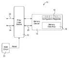
- FIG. 1is a schematic diagram of an embodiment of a system for providing electrical control of write and erase operations in memory devices.
- FIG. 2is a schematic diagram of another embodiment of a system for providing electrical control of write and erase operations in memory devices.
- FIG. 3is a flow chart depicting a method of providing write-protection functionality to a memory device.
- FIG. 1illustrates an example of an embodiment of a system for providing electrical control of write and erase operations in memory devices 10 (system 10 ).
- the system 10includes: a filter logic device 12 ; a memory device 14 including a memory data area 16 and one or more configurable registers 18 ; a system interface 20 ; and a power on reset (POR) circuit 22 .
- the filter logic device 12is responsible for providing secured write-protection functionality to the memory device 14 .
- the system 10 shown in FIG. 1is adapted for use in a slot machine operating using standard PC architecture. However, it is understood that the disclosures provided herein will enable those skilled in the art to implement the system 10 within various microprocessor controlled systems to provide write-protection functionality to memory devices 14 . Accordingly, while the examples provided herein are provided in the context of use in a slot machine, the application of the system 10 is known to be much more broadly applicable.
- POR circuit 22when the system 10 is initially powered up, POR circuit 22 applies a reset signal to the filter logic device 12 .
- the filter logic device 12When the reset signal to the filter logic device 12 becomes inactive, typically after the system 10 reaches stable operating conditions after initial power up, the filter logic device 12 asserts a reset signal through the system interface 20 to the elements of the system 10 other than the memory device 14 (including the remaining elements of the system in which it is embodied, e.g., the slot machine operating using standard PC architecture) to hold the remainder of the system 10 in a reset condition.
- the filter logic device 12then immediately performs a write operation to the configuration registers 18 in the memory device 14 to select the necessary configuration to prevent all further write and/or erase operations to the memory data area 16 and also to prevent any subsequent modification of the configuration register 18 .
- the filter logic device 12asserts a write-protect signal 25 to the memory device 14 , which is held asserted for the entire time the system 10 is active.
- the filter logic device 12then enables the rest of the system 10 to start by de-asserting the reset signal applied through the system interface 20 to the rest of the system 10 .
- the filter logic device 12acts to set the necessary configuration register values to the “protect” state at the beginning of each power-up event, as well as provide a write-protect signal 25 to the memory device 14 to provide complete electrical write-protection for the memory device 14 .
- the example of the system 10 shownis one in which the filter logic device 12 is applied to a memory device 14 that relies solely on configuration registers 18 for write-protection. Because the memory device 14 shown in FIG. 2 does not include an electrical write-protect signal, the configuration registers 18 provide the only write/erase protection. As shown, the filter logic device 12 is provided between the memory device 14 and the system interface 20 to monitor and control any communication from elements of the system 10 to the memory device 14 .
- the POR circuit 22asserts a reset signal to the system interface 20 on startup of the system 10 . Then, if the write-protect signal input 24 to the filter logic device 12 is asserted, while the reset signal is asserted to the system interface 20 , the filter logic device 12 modifies the configurable registers 18 to prevent all further write and erase operations to the memory device 14 . After the filter logic device 12 modifies the configurable registers 18 to prevent all further write and erase operations to the memory device 14 , the POR circuit 22 de-asserts the reset signal to the system interface 20 enabling communication between the system interface 20 and the memory device 14 .
- the method 100includes the steps of: providing a memory device 14 including configurable registers 18 controlling write and erase operations in the memory device 14 ; a system interface 20 ; a filter logic device 12 in electrical communication with the memory device 14 and further in communication with the system interface 20 ; and a POR circuit 22 in communication with the system interface 20 and the filter logic device 12 (step 110 ); on startup of the system 10 , asserting a reset signal to the system interface 20 from the POR circuit 22 (step 120 ); while the reset signal is asserted to the system interface 20 , modifying the configurable registers 18 to prevent all further write and erase operations to the memory device 14 by the filter logic device 12 (step 130 ); and after the filter logic device 12 modifies the configurable registers 18 to prevent all further write and erase operations to the memory device 14 , de-asserting the reset signal from the POR circuit 22 to the system interface 20 thereby enabling communication between the system
Landscapes
- Engineering & Computer Science (AREA)
- Theoretical Computer Science (AREA)
- Computer Security & Cryptography (AREA)
- Software Systems (AREA)
- General Engineering & Computer Science (AREA)
- Physics & Mathematics (AREA)
- General Physics & Mathematics (AREA)
- Computer Hardware Design (AREA)
- Power Engineering (AREA)
- Computer Networks & Wireless Communication (AREA)
- Signal Processing (AREA)
- Storage Device Security (AREA)
Abstract
Description
Claims (12)
Priority Applications (1)
| Application Number | Priority Date | Filing Date | Title |
|---|---|---|---|
| US13/745,746US8971144B2 (en) | 2012-01-19 | 2013-01-18 | Hardware write-protection |
Applications Claiming Priority (2)
| Application Number | Priority Date | Filing Date | Title |
|---|---|---|---|
| US201261588633P | 2012-01-19 | 2012-01-19 | |
| US13/745,746US8971144B2 (en) | 2012-01-19 | 2013-01-18 | Hardware write-protection |
Publications (2)
| Publication Number | Publication Date |
|---|---|
| US20130188437A1 US20130188437A1 (en) | 2013-07-25 |
| US8971144B2true US8971144B2 (en) | 2015-03-03 |
Family
ID=48797079
Family Applications (3)
| Application Number | Title | Priority Date | Filing Date |
|---|---|---|---|
| US13/745,746Expired - Fee RelatedUS8971144B2 (en) | 2012-01-19 | 2013-01-18 | Hardware write-protection |
| US13/745,743Active2034-03-31US9666241B2 (en) | 2012-01-19 | 2013-01-18 | Firmware protection and validation |
| US15/495,753Active2034-04-20US10762210B2 (en) | 2012-01-19 | 2017-04-24 | Firmware protection and validation |
Family Applications After (2)
| Application Number | Title | Priority Date | Filing Date |
|---|---|---|---|
| US13/745,743Active2034-03-31US9666241B2 (en) | 2012-01-19 | 2013-01-18 | Firmware protection and validation |
| US15/495,753Active2034-04-20US10762210B2 (en) | 2012-01-19 | 2017-04-24 | Firmware protection and validation |
Country Status (2)
| Country | Link |
|---|---|
| US (3) | US8971144B2 (en) |
| GB (2) | GB2508252B (en) |
Families Citing this family (22)
| Publication number | Priority date | Publication date | Assignee | Title |
|---|---|---|---|---|
| US10055251B1 (en) | 2009-04-22 | 2018-08-21 | The Trustees Of Columbia University In The City Of New York | Methods, systems, and media for injecting code into embedded devices |
| US9392017B2 (en)* | 2010-04-22 | 2016-07-12 | The Trustees Of Columbia University In The City Of New York | Methods, systems, and media for inhibiting attacks on embedded devices |
| WO2013176711A2 (en) | 2012-02-15 | 2013-11-28 | The Trustees Of Columbia University In The City Of New York | Methods, systems, and media for inhibiting attacks on embedded devices |
| US9449458B2 (en) | 2014-04-07 | 2016-09-20 | Bally Gaming, Inc. | Power cycling of gaming machine |
| US9672361B2 (en)* | 2014-04-30 | 2017-06-06 | Ncr Corporation | Self-service terminal (SST) secure boot |
| CN104332174A (en)* | 2014-11-27 | 2015-02-04 | 天津天地伟业数码科技有限公司 | Memory chip writing protective circuit and memory chip writing protective method applied to security product |
| CN105468964B (en)* | 2015-12-04 | 2018-09-14 | 上海兆芯集成电路有限公司 | Computer system and computer system operation method |
| KR102475458B1 (en)* | 2016-05-30 | 2022-12-08 | 에스케이하이닉스 주식회사 | Power on reset circuit and semiconductor memory device having the same |
| US10268844B2 (en)* | 2016-08-08 | 2019-04-23 | Data I/O Corporation | Embedding foundational root of trust using security algorithms |
| US10346071B2 (en) | 2016-12-29 | 2019-07-09 | Western Digital Technologies, Inc. | Validating firmware for data storage devices |
| CN109426579A (en)* | 2017-08-28 | 2019-03-05 | 西门子公司 | The interruption restoration methods of machine tooling file and the lathe for being applicable in this method |
| US10848474B2 (en)* | 2018-02-26 | 2020-11-24 | Red Hat, Inc. | Firmware validation for encrypted virtual machines |
| JP7287115B2 (en)* | 2019-05-30 | 2023-06-06 | 京セラドキュメントソリューションズ株式会社 | Integrated circuit and integrated circuit control method |
| US11068035B2 (en)* | 2019-09-12 | 2021-07-20 | Dell Products L.P. | Dynamic secure ACPI power resource enumeration objects for embedded devices |
| US11023220B2 (en)* | 2019-09-26 | 2021-06-01 | Dell Products L.P. | Firmware update with integrated smart sequence and action engine |
| CN110716697B (en)* | 2019-09-29 | 2021-09-14 | 联想(北京)有限公司 | Information processing method and equipment |
| US11386234B2 (en)* | 2019-12-17 | 2022-07-12 | Nuvoton Technology Corporation | Security systems and methods for integrated circuits |
| TWI749458B (en)* | 2020-02-05 | 2021-12-11 | 瑞昱半導體股份有限公司 | Verification method and verification system |
| CN114780168B (en)* | 2022-03-30 | 2023-04-28 | 全球能源互联网研究院有限公司南京分公司 | Method and device for dynamically changing security policy of intelligent terminal container and electronic equipment |
| US12124721B2 (en)* | 2022-08-22 | 2024-10-22 | Micron Technology, Inc. | Power safety configurations for logical address space partitions |
| US12373610B1 (en)* | 2022-12-14 | 2025-07-29 | Amazon Technologies, Inc. | Write protection using an immutable root of trust |
| TWI836901B (en)* | 2023-02-14 | 2024-03-21 | 新唐科技股份有限公司 | Firmware switching method for system security and electrical device using the same |
Citations (65)
| Publication number | Priority date | Publication date | Assignee | Title |
|---|---|---|---|---|
| US5592609A (en) | 1994-10-31 | 1997-01-07 | Nintendo Co., Ltd. | Video game/videographics program fabricating system and method with unit based program processing |
| US5599231A (en) | 1994-10-31 | 1997-02-04 | Nintendo Co., Ltd. | Security systems and methods for a videographics and authentication game/program fabricating device |
| US5680533A (en) | 1994-10-31 | 1997-10-21 | Nintendo Co., Ltd. | Videographics program/video game fabricating system and method |
| US5680534A (en) | 1994-10-31 | 1997-10-21 | Nintendo Co., Ltd. | Video game/videographics program fabricating system and method with superimpose control |
| US5724549A (en) | 1992-04-06 | 1998-03-03 | Cyrix Corporation | Cache coherency without bus master arbitration signals |
| US5802583A (en)* | 1996-10-30 | 1998-09-01 | Ramtron International Corporation | Sysyem and method providing selective write protection for individual blocks of memory in a non-volatile memory device |
| US5845332A (en) | 1994-08-03 | 1998-12-01 | Hitachi, Ltd. | Non-volatile memory, memory card and information processing apparatus using the same and method for software write protect control of non-volatile memory |
| US5881002A (en) | 1997-09-29 | 1999-03-09 | Mitsubishi Denki Kabushiki Kaisha | Nonvolatile memory control circuit |
| US5991194A (en) | 1997-10-24 | 1999-11-23 | Jigour; Robin J. | Method and apparatus for providing accessible device information in digital memory devices |
| US6149522A (en) | 1995-06-29 | 2000-11-21 | Silicon Gaming - Nevada | Method of authenticating game data sets in an electronic casino gaming system |
| US20020004905A1 (en) | 1998-07-17 | 2002-01-10 | Derek L Davis | Method for bios authentication prior to bios execution |
| US6379252B2 (en) | 1996-03-28 | 2002-04-30 | Mega Chips Corporation | Game program supply system and program rewrite system |
| US6488581B1 (en) | 1999-06-22 | 2002-12-03 | Igt | Mass storage data protection device for a gaming machine |
| US20030203755A1 (en) | 2002-04-25 | 2003-10-30 | Shuffle Master, Inc. | Encryption in a secure computerized gaming system |
| US6643751B2 (en)* | 2000-03-20 | 2003-11-04 | Texas Instruments Incorporated | System and method for limited access to system memory |
| US20040049645A1 (en) | 2002-09-06 | 2004-03-11 | Jin-Yub Lee | Write-protection blocks for non-volatile semiconductor memory device |
| US6715049B1 (en) | 1997-10-01 | 2004-03-30 | Kabushiki Kaisha Toshiba | Microcomputer and information processing system |
| US20040259633A1 (en) | 2003-04-16 | 2004-12-23 | Gentles Thomas A. | Remote authentication of gaming software in a gaming system environment |
| US20040259640A1 (en) | 2003-04-16 | 2004-12-23 | Gentles Thomas A. | Layered security methods and apparatus in a gaming system environment |
| US20040266523A1 (en) | 2003-04-16 | 2004-12-30 | Gentles Thomas A | Secured networks in a gaming system environment |
| US20040266533A1 (en) | 2003-04-16 | 2004-12-30 | Gentles Thomas A | Gaming software distribution network in a gaming system environment |
| WO2005026951A1 (en) | 2003-09-18 | 2005-03-24 | Aristocrat Technologies Australia Pty Ltd | Bios protection device |
| US6963501B2 (en) | 2003-10-10 | 2005-11-08 | Kabushiki Kaisha Toshiba | Nonvolatile memory |
| US6996721B2 (en)* | 2001-03-27 | 2006-02-07 | Micron Technology, Inc. | Flash device security method utilizing a check register |
| US20060053246A1 (en) | 2004-08-30 | 2006-03-09 | Lee Schweiray J | Systems and methods for providing nonvolatile memory management in wireless phones |
| US7051180B2 (en) | 2002-01-09 | 2006-05-23 | International Business Machines Corporation | Masterless building block binding to partitions using identifiers and indicators |
| US7093091B2 (en) | 2003-09-26 | 2006-08-15 | Atmel Corporation | Selectable block protection for non-volatile memory |
| US20060205513A1 (en) | 2005-03-09 | 2006-09-14 | Igt | MRAM as nonvolatile safe storage for power hit and ESD tolerance in gaming machines |
| US7108605B2 (en) | 2002-09-30 | 2006-09-19 | Igt | EPROM file system in a gaming apparatus |
| US20060248267A1 (en) | 2005-04-29 | 2006-11-02 | Programmable Microelectronics Corporation | Flash memory having configurable sector size and flexible protection scheme |
| US7137893B2 (en) | 2001-05-09 | 2006-11-21 | Wms Gaming Inc. | Method and apparatus for write protecting a gaming storage medium |
| US20070004501A1 (en) | 2005-06-29 | 2007-01-04 | Christopher Brewer | Multi-core processing in a wagering game machine |
| US20070021195A1 (en) | 2005-06-24 | 2007-01-25 | Campbell Steven M | Gaming system file authentication |
| US20070180269A1 (en) | 2006-02-01 | 2007-08-02 | International Business Machines Corporation | I/O address translation blocking in a secure system during power-on-reset |
| US20070300207A1 (en) | 2006-06-22 | 2007-12-27 | James Ronald Booth | Boot Validation System and Method |
| US20080045342A1 (en) | 2003-03-05 | 2008-02-21 | Bally Gaming, Inc. | Data Integrity and Non-Repudiation |
| US20080064501A1 (en) | 2005-04-28 | 2008-03-13 | Bally Gaming, Inc. | Download and configuration capable gaming machine operating system, gaming machine and method |
| US7379341B2 (en)* | 2006-10-05 | 2008-05-27 | Macronix International Co., Ltd. | Loading data with error detection in a power on sequence of flash memory device |
| US7398348B2 (en) | 2004-08-24 | 2008-07-08 | Sandisk 3D Llc | Method and apparatus for using a one-time or few-time programmable memory with a host device designed for erasable/rewritable memory |
| US20080182659A1 (en) | 2007-01-30 | 2008-07-31 | Microsoft Corporation | In-play detection of altered game data |
| US20080254850A1 (en) | 2005-05-06 | 2008-10-16 | Wms Gaming Inc. | Trusted Computing in a Wagering Game Machine |
| US20090124375A1 (en) | 2007-11-09 | 2009-05-14 | Bally Gaming, Inc. | License management method |
| US20090124374A1 (en) | 2007-11-09 | 2009-05-14 | Bally Gaming, Inc. | License management system |
| US20090203430A1 (en) | 2008-02-07 | 2009-08-13 | Igt | Hybrid memory system and spin-buffer journaling in a gaming machine |
| US20090204777A1 (en) | 2005-03-30 | 2009-08-13 | Unity Semiconductor Corporation | Integated circuits and methods to control access to multiple layers of memory |
| US7581256B2 (en) | 2001-08-08 | 2009-08-25 | Igt | Process verification |
| US20090280907A1 (en) | 2008-04-30 | 2009-11-12 | Bally Gaming, Inc. | Server client network throttling system for download content |
| US20090280906A1 (en) | 2008-04-30 | 2009-11-12 | Bally Gaming, Inc. | Server client network throttling method for download content |
| US20100041471A1 (en) | 2006-10-09 | 2010-02-18 | Wms Gaming Inc. | Multiple key failover validation in a wagering game machine |
| US20100048297A1 (en) | 2007-03-01 | 2010-02-25 | Wms Gaming Inc. | Electronic gaming machine security for software stored in nonvolatile media |
| US20100062844A1 (en) | 2003-03-05 | 2010-03-11 | Bally Gaming, Inc. | Authentication and validation systems for gaming devices |
| US20100075760A1 (en) | 2006-07-10 | 2010-03-25 | Wms Gaming Inc. | Partition management in a wagering game system |
| US7694151B1 (en) | 2003-11-20 | 2010-04-06 | Johnson Richard C | Architecture, system, and method for operating on encrypted and/or hidden information |
| US20100120529A1 (en) | 2007-04-04 | 2010-05-13 | Wms Gaming Inc. | Wagering game machine digitally signed volume management |
| US7722468B2 (en) | 2005-03-09 | 2010-05-25 | Igt | Magnetoresistive memory units as read only memory devices in gaming machines |
| US7736234B2 (en) | 2005-03-09 | 2010-06-15 | Igt | MRAM as critical event storage for powered down gaming machines |
| US20100248816A1 (en) | 2007-05-15 | 2010-09-30 | Wms Gaming Inc. | Validation scheduling in a wagering game machine |
| US7827370B2 (en) | 2004-07-08 | 2010-11-02 | Nokia Corporation | Partial permanent write protection of a memory card and partially permanently write protected memory card |
| US20110111865A1 (en) | 2009-11-12 | 2011-05-12 | Bally Gaming, Inc. | Background memory validation for gaming devices |
| US20110118016A1 (en) | 2009-11-13 | 2011-05-19 | Bally Gaming, Inc. | Video Extension Library System and Method |
| US20110118014A1 (en) | 2009-11-16 | 2011-05-19 | Bally Gaming, Inc. | Gaming device having a top box with a reconfigurable pointer |
| US20110115810A1 (en) | 2009-11-16 | 2011-05-19 | Bally Gaming, Inc. | Gaming device having a color reduction filter and related methods |
| US20110117994A1 (en) | 2009-11-16 | 2011-05-19 | Bally Gaming, Inc. | Multi-monitor support for gaming devices and related methods |
| US20110131401A1 (en) | 2009-12-02 | 2011-06-02 | Bally Gaming, Inc. | Authentication system for gaming machines and related methods |
| US7961510B2 (en) | 2008-02-06 | 2011-06-14 | Unity Semiconductor Corporation | Integrated circuits to control access to multiple layers of memory in a solid state drive |
Family Cites Families (8)
| Publication number | Priority date | Publication date | Assignee | Title |
|---|---|---|---|---|
| US6564326B2 (en)* | 1999-07-06 | 2003-05-13 | Walter A. Helbig, Sr. | Method and apparatus for enhancing computer system security |
| US20090193230A1 (en)* | 2008-01-30 | 2009-07-30 | Ralf Findeisen | Computer system including a main processor and a bound security coprocessor |
| US20090247293A1 (en)* | 2008-03-26 | 2009-10-01 | Aristocrat Technologies Australia Pty Limited | Gaming machine |
| US20090327741A1 (en)* | 2008-06-30 | 2009-12-31 | Zimmer Vincent J | System and method to secure boot uefi firmware and uefi-aware operating systems on a mobile internet device (mid) |
| WO2010014109A1 (en)* | 2008-08-01 | 2010-02-04 | Hewlett-Packard Development Company, L.P. | Verifying firmware |
| US8544092B2 (en)* | 2009-03-12 | 2013-09-24 | International Business Machines Corporation | Integrity verification using a peripheral device |
| US9147074B2 (en)* | 2011-05-24 | 2015-09-29 | Cisco Technology, Inc. | Method and apparatus for securing CPUS booted using attached flash memory devices |
| US9015455B2 (en)* | 2011-07-07 | 2015-04-21 | Intel Corporation | Processsor integral technologies for BIOS flash attack protection and notification |
- 2013
- 2013-01-18USUS13/745,746patent/US8971144B2/ennot_activeExpired - Fee Related
- 2013-01-18USUS13/745,743patent/US9666241B2/enactiveActive
- 2013-03-18GBGB1304868.1Apatent/GB2508252B/enactiveActive
- 2013-03-18GBGB1304867.3Apatent/GB2508251B/enactiveActive
- 2017
- 2017-04-24USUS15/495,753patent/US10762210B2/enactiveActive
Patent Citations (74)
| Publication number | Priority date | Publication date | Assignee | Title |
|---|---|---|---|---|
| US5724549A (en) | 1992-04-06 | 1998-03-03 | Cyrix Corporation | Cache coherency without bus master arbitration signals |
| US5845332A (en) | 1994-08-03 | 1998-12-01 | Hitachi, Ltd. | Non-volatile memory, memory card and information processing apparatus using the same and method for software write protect control of non-volatile memory |
| US5599231A (en) | 1994-10-31 | 1997-02-04 | Nintendo Co., Ltd. | Security systems and methods for a videographics and authentication game/program fabricating device |
| US5680533A (en) | 1994-10-31 | 1997-10-21 | Nintendo Co., Ltd. | Videographics program/video game fabricating system and method |
| US5680534A (en) | 1994-10-31 | 1997-10-21 | Nintendo Co., Ltd. | Video game/videographics program fabricating system and method with superimpose control |
| US5592609A (en) | 1994-10-31 | 1997-01-07 | Nintendo Co., Ltd. | Video game/videographics program fabricating system and method with unit based program processing |
| US6149522A (en) | 1995-06-29 | 2000-11-21 | Silicon Gaming - Nevada | Method of authenticating game data sets in an electronic casino gaming system |
| US6379252B2 (en) | 1996-03-28 | 2002-04-30 | Mega Chips Corporation | Game program supply system and program rewrite system |
| US5802583A (en)* | 1996-10-30 | 1998-09-01 | Ramtron International Corporation | Sysyem and method providing selective write protection for individual blocks of memory in a non-volatile memory device |
| US5881002A (en) | 1997-09-29 | 1999-03-09 | Mitsubishi Denki Kabushiki Kaisha | Nonvolatile memory control circuit |
| US6715049B1 (en) | 1997-10-01 | 2004-03-30 | Kabushiki Kaisha Toshiba | Microcomputer and information processing system |
| US5991194A (en) | 1997-10-24 | 1999-11-23 | Jigour; Robin J. | Method and apparatus for providing accessible device information in digital memory devices |
| US20020004905A1 (en) | 1998-07-17 | 2002-01-10 | Derek L Davis | Method for bios authentication prior to bios execution |
| US6875109B2 (en) | 1999-06-22 | 2005-04-05 | Igt | Mass storage data protection system for a gaming machine |
| US6488581B1 (en) | 1999-06-22 | 2002-12-03 | Igt | Mass storage data protection device for a gaming machine |
| US6643751B2 (en)* | 2000-03-20 | 2003-11-04 | Texas Instruments Incorporated | System and method for limited access to system memory |
| US6996721B2 (en)* | 2001-03-27 | 2006-02-07 | Micron Technology, Inc. | Flash device security method utilizing a check register |
| US7137893B2 (en) | 2001-05-09 | 2006-11-21 | Wms Gaming Inc. | Method and apparatus for write protecting a gaming storage medium |
| US7581256B2 (en) | 2001-08-08 | 2009-08-25 | Igt | Process verification |
| US7996916B2 (en) | 2001-08-08 | 2011-08-09 | Igt | Process verification |
| US7051180B2 (en) | 2002-01-09 | 2006-05-23 | International Business Machines Corporation | Masterless building block binding to partitions using identifiers and indicators |
| US20030203755A1 (en) | 2002-04-25 | 2003-10-30 | Shuffle Master, Inc. | Encryption in a secure computerized gaming system |
| US20040049645A1 (en) | 2002-09-06 | 2004-03-11 | Jin-Yub Lee | Write-protection blocks for non-volatile semiconductor memory device |
| US7210012B2 (en)* | 2002-09-06 | 2007-04-24 | Samsung Electronics Co., Ltd. | Write-protection blocks for non-volatile semiconductor memory device |
| US7108605B2 (en) | 2002-09-30 | 2006-09-19 | Igt | EPROM file system in a gaming apparatus |
| US20100062844A1 (en) | 2003-03-05 | 2010-03-11 | Bally Gaming, Inc. | Authentication and validation systems for gaming devices |
| US20080045342A1 (en) | 2003-03-05 | 2008-02-21 | Bally Gaming, Inc. | Data Integrity and Non-Repudiation |
| US20040266533A1 (en) | 2003-04-16 | 2004-12-30 | Gentles Thomas A | Gaming software distribution network in a gaming system environment |
| US20040266523A1 (en) | 2003-04-16 | 2004-12-30 | Gentles Thomas A | Secured networks in a gaming system environment |
| US20040259640A1 (en) | 2003-04-16 | 2004-12-23 | Gentles Thomas A. | Layered security methods and apparatus in a gaming system environment |
| US20040259633A1 (en) | 2003-04-16 | 2004-12-23 | Gentles Thomas A. | Remote authentication of gaming software in a gaming system environment |
| WO2005026951A1 (en) | 2003-09-18 | 2005-03-24 | Aristocrat Technologies Australia Pty Ltd | Bios protection device |
| US7093091B2 (en) | 2003-09-26 | 2006-08-15 | Atmel Corporation | Selectable block protection for non-volatile memory |
| US7325114B2 (en) | 2003-09-26 | 2008-01-29 | Atmel Corporation | Selectable block protection for non-volatile memory |
| US7275128B2 (en) | 2003-09-26 | 2007-09-25 | Atmel Corporation | Selectable block protection for non-volatile memory |
| US6963501B2 (en) | 2003-10-10 | 2005-11-08 | Kabushiki Kaisha Toshiba | Nonvolatile memory |
| US7694151B1 (en) | 2003-11-20 | 2010-04-06 | Johnson Richard C | Architecture, system, and method for operating on encrypted and/or hidden information |
| US7827370B2 (en) | 2004-07-08 | 2010-11-02 | Nokia Corporation | Partial permanent write protection of a memory card and partially permanently write protected memory card |
| US20110047416A1 (en) | 2004-08-24 | 2011-02-24 | Moore Christopher S | Method and Apparatus for Using a One-Time or Few-Time Programmable Memory with a Host Device Designed for Erasable-Rewriteable Memory |
| US7861058B2 (en) | 2004-08-24 | 2010-12-28 | Sandisk 3D Llc | Method and apparatus for using a one-time or few-time programmable memory with a host device designed for erasable/rewriteable memory |
| US7689805B2 (en) | 2004-08-24 | 2010-03-30 | Sandisk 3D Llc | Method and apparatus for using a one-time or few-time programmable memory with a host device designed for erasable/rewriteable memory |
| US7398348B2 (en) | 2004-08-24 | 2008-07-08 | Sandisk 3D Llc | Method and apparatus for using a one-time or few-time programmable memory with a host device designed for erasable/rewritable memory |
| US20060053246A1 (en) | 2004-08-30 | 2006-03-09 | Lee Schweiray J | Systems and methods for providing nonvolatile memory management in wireless phones |
| US20060205513A1 (en) | 2005-03-09 | 2006-09-14 | Igt | MRAM as nonvolatile safe storage for power hit and ESD tolerance in gaming machines |
| US7736234B2 (en) | 2005-03-09 | 2010-06-15 | Igt | MRAM as critical event storage for powered down gaming machines |
| US7722468B2 (en) | 2005-03-09 | 2010-05-25 | Igt | Magnetoresistive memory units as read only memory devices in gaming machines |
| US20090204777A1 (en) | 2005-03-30 | 2009-08-13 | Unity Semiconductor Corporation | Integated circuits and methods to control access to multiple layers of memory |
| US20080064501A1 (en) | 2005-04-28 | 2008-03-13 | Bally Gaming, Inc. | Download and configuration capable gaming machine operating system, gaming machine and method |
| US20060248267A1 (en) | 2005-04-29 | 2006-11-02 | Programmable Microelectronics Corporation | Flash memory having configurable sector size and flexible protection scheme |
| US20080254850A1 (en) | 2005-05-06 | 2008-10-16 | Wms Gaming Inc. | Trusted Computing in a Wagering Game Machine |
| US20070021195A1 (en) | 2005-06-24 | 2007-01-25 | Campbell Steven M | Gaming system file authentication |
| US20070004501A1 (en) | 2005-06-29 | 2007-01-04 | Christopher Brewer | Multi-core processing in a wagering game machine |
| US20070180269A1 (en) | 2006-02-01 | 2007-08-02 | International Business Machines Corporation | I/O address translation blocking in a secure system during power-on-reset |
| US20070300207A1 (en) | 2006-06-22 | 2007-12-27 | James Ronald Booth | Boot Validation System and Method |
| US20100075760A1 (en) | 2006-07-10 | 2010-03-25 | Wms Gaming Inc. | Partition management in a wagering game system |
| US7379341B2 (en)* | 2006-10-05 | 2008-05-27 | Macronix International Co., Ltd. | Loading data with error detection in a power on sequence of flash memory device |
| US20100041471A1 (en) | 2006-10-09 | 2010-02-18 | Wms Gaming Inc. | Multiple key failover validation in a wagering game machine |
| US20080182659A1 (en) | 2007-01-30 | 2008-07-31 | Microsoft Corporation | In-play detection of altered game data |
| US20100048297A1 (en) | 2007-03-01 | 2010-02-25 | Wms Gaming Inc. | Electronic gaming machine security for software stored in nonvolatile media |
| US20100120529A1 (en) | 2007-04-04 | 2010-05-13 | Wms Gaming Inc. | Wagering game machine digitally signed volume management |
| US20100248816A1 (en) | 2007-05-15 | 2010-09-30 | Wms Gaming Inc. | Validation scheduling in a wagering game machine |
| US20090124375A1 (en) | 2007-11-09 | 2009-05-14 | Bally Gaming, Inc. | License management method |
| US20090124374A1 (en) | 2007-11-09 | 2009-05-14 | Bally Gaming, Inc. | License management system |
| US7961510B2 (en) | 2008-02-06 | 2011-06-14 | Unity Semiconductor Corporation | Integrated circuits to control access to multiple layers of memory in a solid state drive |
| US7990762B2 (en) | 2008-02-06 | 2011-08-02 | Unity Semiconductor Corporation | Integrated circuits to control access to multiple layers of memory |
| US20090203430A1 (en) | 2008-02-07 | 2009-08-13 | Igt | Hybrid memory system and spin-buffer journaling in a gaming machine |
| US20090280907A1 (en) | 2008-04-30 | 2009-11-12 | Bally Gaming, Inc. | Server client network throttling system for download content |
| US20090280906A1 (en) | 2008-04-30 | 2009-11-12 | Bally Gaming, Inc. | Server client network throttling method for download content |
| US20110111865A1 (en) | 2009-11-12 | 2011-05-12 | Bally Gaming, Inc. | Background memory validation for gaming devices |
| US20110118016A1 (en) | 2009-11-13 | 2011-05-19 | Bally Gaming, Inc. | Video Extension Library System and Method |
| US20110117994A1 (en) | 2009-11-16 | 2011-05-19 | Bally Gaming, Inc. | Multi-monitor support for gaming devices and related methods |
| US20110115810A1 (en) | 2009-11-16 | 2011-05-19 | Bally Gaming, Inc. | Gaming device having a color reduction filter and related methods |
| US20110118014A1 (en) | 2009-11-16 | 2011-05-19 | Bally Gaming, Inc. | Gaming device having a top box with a reconfigurable pointer |
| US20110131401A1 (en) | 2009-12-02 | 2011-06-02 | Bally Gaming, Inc. | Authentication system for gaming machines and related methods |
Also Published As
| Publication number | Publication date |
|---|---|
| GB2508251B (en) | 2020-01-15 |
| GB2508252B (en) | 2015-10-28 |
| US9666241B2 (en) | 2017-05-30 |
| US10762210B2 (en) | 2020-09-01 |
| US20130191624A1 (en) | 2013-07-25 |
| GB2508252A (en) | 2014-05-28 |
| GB201304868D0 (en) | 2013-05-01 |
| US20170228543A1 (en) | 2017-08-10 |
| GB201304867D0 (en) | 2013-05-01 |
| GB2508251A (en) | 2014-05-28 |
| US20130188437A1 (en) | 2013-07-25 |
Similar Documents
| Publication | Publication Date | Title |
|---|---|---|
| US8971144B2 (en) | Hardware write-protection | |
| US7107460B2 (en) | Method and system for securing enablement access to a data security device | |
| US6026016A (en) | Methods and apparatus for hardware block locking in a nonvolatile memory | |
| US6188602B1 (en) | Mechanism to commit data to a memory device with read-only access | |
| US20030200453A1 (en) | Control function with multiple security states for facilitating secure operation of an integrated system | |
| US20060209595A1 (en) | Systems and methods for write protection of non-volatile memory devices | |
| US20090113114A1 (en) | Implementation of One Time Programmable Memory with Embedded Flash Memory in a System-on-Chip | |
| US20130117499A1 (en) | Reversible write-protection for non-volatile semiconductor memory device | |
| US20170032126A1 (en) | Information processing device, controller and method of controlling information processing device | |
| US8621298B2 (en) | Apparatus for protecting against external attack for processor based on arm core and method using the same | |
| US10037206B2 (en) | Methods and systems for state switching | |
| KR20150033695A (en) | Memory protection | |
| US8621195B2 (en) | Disabling communication ports | |
| CN101436260B (en) | Data processing circuit and communication mobile terminal device | |
| US20100037000A1 (en) | One-time-programmable memory emulation | |
| EP3413195B1 (en) | Processing system, related integrated circuit, device and method | |
| EP2257860A2 (en) | Method and apparatus for hardware reset protection | |
| CN111191214B (en) | Embedded processor and data protection method | |
| US20070239996A1 (en) | Method and apparatus for binding computer memory to motherboard | |
| US10452844B2 (en) | Protecting isolated secret data of integrated circuit devices | |
| US9032540B2 (en) | Access system and method thereof | |
| US20200194083A1 (en) | Data processing system and data processing method | |
| US8510501B2 (en) | Write-protection system and method thereof | |
| CN117150583A (en) | Access protection method and device applied to PNOR flash | |
| US9202073B2 (en) | Security measures for data protection |
Legal Events
| Date | Code | Title | Description |
|---|---|---|---|
| AS | Assignment | Owner name:QUIXANT, LTD., UNITED KINGDOM Free format text:ASSIGNMENT OF ASSIGNORS INTEREST;ASSIGNOR:JARMANY, NICHOLAS CHARLES LEOPOLD;REEL/FRAME:029661/0373 Effective date:20120119 | |
| AS | Assignment | Owner name:QUIXANT PLC, UNITED KINGDOM Free format text:CHANGE OF NAME;ASSIGNOR:QUIXANT LIMITED;REEL/FRAME:034787/0114 Effective date:20130429 | |
| STCF | Information on status: patent grant | Free format text:PATENTED CASE | |
| CC | Certificate of correction | ||
| MAFP | Maintenance fee payment | Free format text:PAYMENT OF MAINTENANCE FEE, 4TH YR, SMALL ENTITY (ORIGINAL EVENT CODE: M2551); ENTITY STATUS OF PATENT OWNER: SMALL ENTITY Year of fee payment:4 | |
| FEPP | Fee payment procedure | Free format text:MAINTENANCE FEE REMINDER MAILED (ORIGINAL EVENT CODE: REM.); ENTITY STATUS OF PATENT OWNER: SMALL ENTITY | |
| LAPS | Lapse for failure to pay maintenance fees | Free format text:PATENT EXPIRED FOR FAILURE TO PAY MAINTENANCE FEES (ORIGINAL EVENT CODE: EXP.); ENTITY STATUS OF PATENT OWNER: SMALL ENTITY | |
| STCH | Information on status: patent discontinuation | Free format text:PATENT EXPIRED DUE TO NONPAYMENT OF MAINTENANCE FEES UNDER 37 CFR 1.362 | |
| FP | Lapsed due to failure to pay maintenance fee | Effective date:20230303 |