US8967992B2 - Optically absorptive material for alignment marks - Google Patents
Optically absorptive material for alignment marksDownload PDFInfo
- Publication number
- US8967992B2 US8967992B2US13/455,966US201213455966AUS8967992B2US 8967992 B2US8967992 B2US 8967992B2US 201213455966 AUS201213455966 AUS 201213455966AUS 8967992 B2US8967992 B2US 8967992B2
- Authority
- US
- United States
- Prior art keywords
- template
- absorptive material
- substrate
- alignment
- contrast
- Prior art date
- Legal status (The legal status is an assumption and is not a legal conclusion. Google has not performed a legal analysis and makes no representation as to the accuracy of the status listed.)
- Active, expires
Links
Images


Classifications
- H—ELECTRICITY
- H01—ELECTRIC ELEMENTS
- H01L—SEMICONDUCTOR DEVICES NOT COVERED BY CLASS H10
- H01L21/00—Processes or apparatus adapted for the manufacture or treatment of semiconductor or solid state devices or of parts thereof
- H01L21/02—Manufacture or treatment of semiconductor devices or of parts thereof
- H01L21/027—Making masks on semiconductor bodies for further photolithographic processing not provided for in group H01L21/18 or H01L21/34
- G—PHYSICS
- G03—PHOTOGRAPHY; CINEMATOGRAPHY; ANALOGOUS TECHNIQUES USING WAVES OTHER THAN OPTICAL WAVES; ELECTROGRAPHY; HOLOGRAPHY
- G03F—PHOTOMECHANICAL PRODUCTION OF TEXTURED OR PATTERNED SURFACES, e.g. FOR PRINTING, FOR PROCESSING OF SEMICONDUCTOR DEVICES; MATERIALS THEREFOR; ORIGINALS THEREFOR; APPARATUS SPECIALLY ADAPTED THEREFOR
- G03F7/00—Photomechanical, e.g. photolithographic, production of textured or patterned surfaces, e.g. printing surfaces; Materials therefor, e.g. comprising photoresists; Apparatus specially adapted therefor
- G03F7/0002—Lithographic processes using patterning methods other than those involving the exposure to radiation, e.g. by stamping
- B—PERFORMING OPERATIONS; TRANSPORTING
- B29—WORKING OF PLASTICS; WORKING OF SUBSTANCES IN A PLASTIC STATE IN GENERAL
- B29C—SHAPING OR JOINING OF PLASTICS; SHAPING OF MATERIAL IN A PLASTIC STATE, NOT OTHERWISE PROVIDED FOR; AFTER-TREATMENT OF THE SHAPED PRODUCTS, e.g. REPAIRING
- B29C43/00—Compression moulding, i.e. applying external pressure to flow the moulding material; Apparatus therefor
- B29C43/32—Component parts, details or accessories; Auxiliary operations
- B29C43/58—Measuring, controlling or regulating
- B—PERFORMING OPERATIONS; TRANSPORTING
- B29—WORKING OF PLASTICS; WORKING OF SUBSTANCES IN A PLASTIC STATE IN GENERAL
- B29C—SHAPING OR JOINING OF PLASTICS; SHAPING OF MATERIAL IN A PLASTIC STATE, NOT OTHERWISE PROVIDED FOR; AFTER-TREATMENT OF THE SHAPED PRODUCTS, e.g. REPAIRING
- B29C59/00—Surface shaping of articles, e.g. embossing; Apparatus therefor
- B—PERFORMING OPERATIONS; TRANSPORTING
- B82—NANOTECHNOLOGY
- B82Y—SPECIFIC USES OR APPLICATIONS OF NANOSTRUCTURES; MEASUREMENT OR ANALYSIS OF NANOSTRUCTURES; MANUFACTURE OR TREATMENT OF NANOSTRUCTURES
- B82Y10/00—Nanotechnology for information processing, storage or transmission, e.g. quantum computing or single electron logic
- B—PERFORMING OPERATIONS; TRANSPORTING
- B82—NANOTECHNOLOGY
- B82Y—SPECIFIC USES OR APPLICATIONS OF NANOSTRUCTURES; MEASUREMENT OR ANALYSIS OF NANOSTRUCTURES; MANUFACTURE OR TREATMENT OF NANOSTRUCTURES
- B82Y40/00—Manufacture or treatment of nanostructures
- G—PHYSICS
- G03—PHOTOGRAPHY; CINEMATOGRAPHY; ANALOGOUS TECHNIQUES USING WAVES OTHER THAN OPTICAL WAVES; ELECTROGRAPHY; HOLOGRAPHY
- G03F—PHOTOMECHANICAL PRODUCTION OF TEXTURED OR PATTERNED SURFACES, e.g. FOR PRINTING, FOR PROCESSING OF SEMICONDUCTOR DEVICES; MATERIALS THEREFOR; ORIGINALS THEREFOR; APPARATUS SPECIALLY ADAPTED THEREFOR
- G03F9/00—Registration or positioning of originals, masks, frames, photographic sheets or textured or patterned surfaces, e.g. automatically
- G03F9/70—Registration or positioning of originals, masks, frames, photographic sheets or textured or patterned surfaces, e.g. automatically for microlithography
- G03F9/7003—Alignment type or strategy, e.g. leveling, global alignment
- G03F9/7042—Alignment for lithographic apparatus using patterning methods other than those involving the exposure to radiation, e.g. by stamping or imprinting
- G—PHYSICS
- G03—PHOTOGRAPHY; CINEMATOGRAPHY; ANALOGOUS TECHNIQUES USING WAVES OTHER THAN OPTICAL WAVES; ELECTROGRAPHY; HOLOGRAPHY
- G03F—PHOTOMECHANICAL PRODUCTION OF TEXTURED OR PATTERNED SURFACES, e.g. FOR PRINTING, FOR PROCESSING OF SEMICONDUCTOR DEVICES; MATERIALS THEREFOR; ORIGINALS THEREFOR; APPARATUS SPECIALLY ADAPTED THEREFOR
- G03F9/00—Registration or positioning of originals, masks, frames, photographic sheets or textured or patterned surfaces, e.g. automatically
- G03F9/70—Registration or positioning of originals, masks, frames, photographic sheets or textured or patterned surfaces, e.g. automatically for microlithography
- G03F9/7073—Alignment marks and their environment
- G03F9/7084—Position of mark on substrate, i.e. position in (x, y, z) of mark, e.g. buried or resist covered mark, mark on rearside, at the substrate edge, in the circuit area, latent image mark, marks in plural levels
- B—PERFORMING OPERATIONS; TRANSPORTING
- B29—WORKING OF PLASTICS; WORKING OF SUBSTANCES IN A PLASTIC STATE IN GENERAL
- B29C—SHAPING OR JOINING OF PLASTICS; SHAPING OF MATERIAL IN A PLASTIC STATE, NOT OTHERWISE PROVIDED FOR; AFTER-TREATMENT OF THE SHAPED PRODUCTS, e.g. REPAIRING
- B29C43/00—Compression moulding, i.e. applying external pressure to flow the moulding material; Apparatus therefor
- B29C43/32—Component parts, details or accessories; Auxiliary operations
- B29C43/58—Measuring, controlling or regulating
- B29C2043/585—Measuring, controlling or regulating detecting defects, e.g. foreign matter between the moulds, inaccurate position, breakage
- B—PERFORMING OPERATIONS; TRANSPORTING
- B29—WORKING OF PLASTICS; WORKING OF SUBSTANCES IN A PLASTIC STATE IN GENERAL
- B29K—INDEXING SCHEME ASSOCIATED WITH SUBCLASSES B29B, B29C OR B29D, RELATING TO MOULDING MATERIALS OR TO MATERIALS FOR MOULDS, REINFORCEMENTS, FILLERS OR PREFORMED PARTS, e.g. INSERTS
- B29K2105/00—Condition, form or state of moulded material or of the material to be shaped
- B29K2105/24—Condition, form or state of moulded material or of the material to be shaped crosslinked or vulcanised
- B—PERFORMING OPERATIONS; TRANSPORTING
- B29—WORKING OF PLASTICS; WORKING OF SUBSTANCES IN A PLASTIC STATE IN GENERAL
- B29K—INDEXING SCHEME ASSOCIATED WITH SUBCLASSES B29B, B29C OR B29D, RELATING TO MOULDING MATERIALS OR TO MATERIALS FOR MOULDS, REINFORCEMENTS, FILLERS OR PREFORMED PARTS, e.g. INSERTS
- B29K2905/00—Use of metals, their alloys or their compounds, as mould material
- B29K2905/02—Aluminium
- B—PERFORMING OPERATIONS; TRANSPORTING
- B29—WORKING OF PLASTICS; WORKING OF SUBSTANCES IN A PLASTIC STATE IN GENERAL
- B29K—INDEXING SCHEME ASSOCIATED WITH SUBCLASSES B29B, B29C OR B29D, RELATING TO MOULDING MATERIALS OR TO MATERIALS FOR MOULDS, REINFORCEMENTS, FILLERS OR PREFORMED PARTS, e.g. INSERTS
- B29K2995/00—Properties of moulding materials, reinforcements, fillers, preformed parts or moulds
- B29K2995/0018—Properties of moulding materials, reinforcements, fillers, preformed parts or moulds having particular optical properties, e.g. fluorescent or phosphorescent
- B29K2995/0026—Transparent
- B29K2995/0027—Transparent for light outside the visible spectrum
- Y—GENERAL TAGGING OF NEW TECHNOLOGICAL DEVELOPMENTS; GENERAL TAGGING OF CROSS-SECTIONAL TECHNOLOGIES SPANNING OVER SEVERAL SECTIONS OF THE IPC; TECHNICAL SUBJECTS COVERED BY FORMER USPC CROSS-REFERENCE ART COLLECTIONS [XRACs] AND DIGESTS
- Y10—TECHNICAL SUBJECTS COVERED BY FORMER USPC
- Y10T—TECHNICAL SUBJECTS COVERED BY FORMER US CLASSIFICATION
- Y10T428/00—Stock material or miscellaneous articles
- Y10T428/24—Structurally defined web or sheet [e.g., overall dimension, etc.]
- Y10T428/24479—Structurally defined web or sheet [e.g., overall dimension, etc.] including variation in thickness
- Y10T428/24612—Composite web or sheet
- Y10T428/2462—Composite web or sheet with partial filling of valleys on outer surface
Definitions
- Nano-fabricationincludes the fabrication of very small structures that have features on the order of 100 nanometers or smaller.
- One application in which nano-fabrication has had a sizeable impactis in the processing of integrated circuits.
- the semiconductor processing industrycontinues to strive for larger production yields while increasing the circuits per unit area formed on a substrate; therefore nano-fabrication becomes increasingly important.
- Nano-fabricationprovides greater process control while allowing continued reduction of the minimum feature dimensions of the structures formed.
- Other areas of development in which nano-fabrication has been employedinclude biotechnology, optical technology, mechanical systems, and the like.
- imprint lithographyAn exemplary nano-fabrication technique in use today is commonly referred to as imprint lithography.
- Exemplary imprint lithography processesare described in detail in numerous publications, such as U.S. Patent Publication No. 2004/0065976, U.S. Patent Publication No. 2004/0065252, and U.S. Pat. No. 6,936,194, all of which are hereby incorporated by reference herein.
- An imprint lithography technique disclosed in each of the aforementioned U.S. patent publications and patentincludes formation of a relief pattern in a formable (polymerizable) layer and transferring a pattern corresponding to the relief pattern into an underlying substrate.
- the substratemay be coupled to a motion stage to obtain a desired positioning to facilitate the patterning process.
- the patterning processuses a template spaced apart from the substrate and a formable liquid applied between the template and the substrate.
- the formable liquidis solidified to form a rigid layer that has a pattern conforming to a shape of the surface of the template that contacts the formable liquid.
- the templateis separated from the rigid layer such that the template and the substrate are spaced apart.
- the substrate and the solidified layerare then subjected to additional processes to transfer a relief image into the substrate that corresponds to the pattern in the solidified layer.
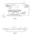
- FIG. 1illustrates a simplified side view of a lithographic system.
- FIG. 2illustrates a simplified side view of the substrate illustrated in FIG. 1 , having a patterned layer thereon.
- FIG. 3Aillustrates a simplified bottom view of a template having pattern features and alignment marks thereon.
- FIG. 3Billustrates an enlarged view of an alignment mark illustrated in FIG. 3A .
- FIG. 4Aillustrates a simplified side view of a template and substrate having corresponding alignment marks partially filled with a formable material.
- FIG. 4Billustrates an image associated with FIG. 4A .
- FIG. 4Cillustrates a schematic depiction of the contrast signal of FIG. 4B .
- FIG. 5 of theillustrates a simplified side view of a template and substrate having corresponding alignment marks partially filled with a formable material according to an embodiment of the invention.
- FIGS. 6A-6Billustrate diffraction conditions and electric fields for a simplified alignment mark grating.
- FIGS. 7A-7Billustrate diffraction conditions and electric field for a simplified alignment mark grating according to an embodiment of the invention.
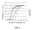
- FIG. 8illustrates contrast levels generated from alignment marks according to embodiments of the invention.
- a lithographic system 10used to form a relief pattern on substrate 12 .
- Substrate 12may be coupled to substrate chuck 14 .
- substrate chuck 14is a vacuum chuck.
- Substrate chuck 14may be any chuck including, but not limited to, vacuum, pin-type, groove-type, electrostatic, electromagnetic, and/or the like. Exemplary chucks are described in U.S. Pat. No. 6,873,087, which is hereby incorporated by reference herein.
- Stage 16may provide translational and/or rotational motion along the x, y, and z-axes. Stage 16 , substrate 12 , and substrate chuck 14 may also be positioned on a base (not shown).
- Template 18Spaced-apart from substrate 12 is template 18 .
- Template 18may include a body having a first side and a second side with one side having a mesa 20 extending therefrom towards substrate 12 .
- Mesa 20having a patterning surface 22 thereon.
- mesa 20may be referred to as mold 20 .
- template 18may be formed without mesa 20 .
- Template 18 and/or mold 20may be formed from such materials including, but not limited to, fused-silica, quartz, silicon, organic polymers, siloxane polymers, borosilicate glass, fluorocarbon polymers, metal, hardened sapphire, and/or the like.
- patterning surface 22comprises features defined by a plurality of spaced-apart recesses 24 and/or protrusions 26 , though embodiments of the present invention are not limited to such configurations (e.g., planar surface). Patterning surface 22 may define any original pattern that forms the basis of a pattern to be formed on substrate 12 .
- Template 18may be coupled to chuck 28 .
- Chuck 28may be configured as, but not limited to, vacuum, pin-type, groove-type, electrostatic, electromagnetic, and/or other similar chuck types. Exemplary chucks are further described in U.S. Pat. No. 6,873,087, which is hereby incorporated by reference herein. Further, chuck 28 may be coupled to imprint head 30 such that chuck 28 and/or imprint head 30 may be configured to facilitate movement of template 18 .
- System 10may further comprise a fluid dispense system 32 .
- Fluid dispense system 32may be used to deposit formable material 34 (e.g., polymerizable material) on substrate 12 .
- Formable material 34may be positioned upon substrate 12 using techniques, such as, drop dispense, spin-coating, dip coating, chemical vapor deposition (CVD), physical vapor deposition (PVD), thin film deposition, thick film deposition, and/or the like.
- Formable material 34may be disposed upon substrate 12 before and/or after a desired volume is defined between mold 22 and substrate 12 depending on design considerations.
- Formable material 34may be functional nano-particles having use within the bio-domain, solar cell industry, battery industry, and/or other industries requiring a functional nano-particle.
- formable material 34may comprise a monomer mixture as described in U.S. Pat. No. 7,157,036 and U.S. Patent Publication No. 2005/0187339, both of which are herein incorporated by reference.
- formable material 34may include, but is not limited to, biomaterials (e.g., PEG), solar cell materials (e.g., N-type, P-type materials), and/or the like.
- system 10may further comprise energy source 38 coupled to direct energy 40 along path 42 .
- Imprint head 30 and stage 16may be configured to position template 18 and substrate 12 in superimposition with path 42 .
- System 10may be regulated by processor 54 in communication with stage 16 , imprint head 30 , fluid dispense system 32 , and/or source 38 , and may operate on a computer readable program stored in memory 56 .
- Either imprint head 30 , stage 16 , or bothvary a distance between mold 20 and substrate 12 to define a desired volume therebetween that is filled by formable material 34 .
- imprint head 30may apply a force to template 18 such that mold 20 contacts formable material 34 .
- source 38produces energy 40 , e.g., ultraviolet radiation, causing formable material 34 to solidify and/or cross-link conforming to a shape of surface 44 of substrate 12 and patterning surface 22 , defining patterned layer 46 on substrate 12 .
- Patterned layer 46may comprise a residual layer 48 and a plurality of features shown as protrusions 50 and recessions 52 , with protrusions 50 having a thickness t 1 and residual layer having a thickness t 2 .
- Alignment marksmay aid in aligning template 18 and substrate 12 prior to imprinting formable material 34 in order to facilitate pattern transfer to a precise location on the substrate and correct for any overlay error between template and substrate. Alignment and registration of features across multiple lithography steps is important for overall process success and device fabrication. As feature sizes reach ever smaller dimensions, the demands placed on lithographic placement accuracy become enormous. With particular regard to imprint lithography methods, alignment is further complicated by the mechanical interaction of the template, substrate, and formable material. Exemplary alignment systems and processes that may aid in the facilitation of pattern transfer are further described in U.S. Ser. No. 12/175,258 (issued as U.S. Pat. No. 7,837,907), U.S. Ser. No.
- alignment marksmay be etched into e.g. quartz or fused silica, mediums having a substantially similar index of refraction as formable material 34 .
- formable material 34e.g. quartz or fused silica, mediums having a substantially similar index of refraction as formable material 34 .
- the optical contrast necessary to resolve alignment features within the visible spectrumno longer exists. That is, the closely matched values of the indices of refraction for the quartz or fused silica templates on the one hand and formable materials (e.g., organic resist materials) on the other hand, result in a lack of visible contrast when the template alignment features are fully filled with formable material during imprinting.
- trenchesmay result in large open spaces on substrate 12 that may be detrimental to some processes such as chemical-mechanical planarization (CMP), polishing, and/or etching processes wherein uniformity and consistent feature density may be significant attributes.
- CMPchemical-mechanical planarization
- Such trench regionsare also prime locations for defectivity. For example, such open areas are more susceptible to contamination, because formable material vapor may deposit and build up over time in these areas.
- alignment markscan be formed of high contrast materials.
- the high contrast materials (HCM) used to form alignment marksmay have different indices of refraction than the formable material 34 . As such, these alignment marks may remain visible even in the presence of formable material 34 for aligning processes.
- Such high contrast alignment marksmay be patterned in the same step as the primary patterning features of template 18 , and by patterning in the same step, pattern placement errors may be minimized.
- These alignment marksmay be generally etched to substantially the same depth as the primary features formed in substrate 12 .
- FIGS. 3A and 3Bdepicts template 18 having patterned mold 20 with patterned feature area 36 and with alignment marks 60 located peripheral to the corners of patterned feature area 36 .
- alignment mark 60includes recesses 64 and protrusions 66 , with high contrast material 62 having a high index of refraction located in recesses 64 .
- Substrate 12contains corresponding alignment marks 80 in superimposition with alignment marks 60 .
- formable material 34is in the process of spreading and filling recesses 64 of alignment mark 60 .
- FIG. 4Bis illustrative of the image and its contrast generated by an alignment mark in the partially filled state of FIG. 4A .
- contrastmeans a normalized difference between maximum and minimum intensities in the moiré pattern.
- Intensity variation along moiré patterncomes from the fact that different areas of align marks on the template such as protuded and recessed parts of the align mark shown of FIG. 4A as dark and light areas, and extruded and depressed parts of the corresponding pattern on substrate give different contribution to the scattered light. Superposition of light from all those scatter areas results in intensity variation along an observed Moiré pattern. Both light amplitude and optical phase difference are important for such superposition.
- FIG. 4Cfurther provides a schematic depiction of such signal distortion, showing schematically the intensity distribution (dashed line S 1 ) on the upper moiré strip reproduced from FIG. 4B .
- the intensityis taken along the dashed white line D that overlaps the image of the moiré pattern in FIG. 4C .
- a good moiré pattern useful for alignmentshould generate a signal similar to the solid line S 2 in FIG. 4C , and within even maximum and minimum intensities.
- Described hereinare template alignment marks and related processes that utilize highly optically absorptive material (i.e., material with a high extinction coefficient) of a sufficient thickness that significantly reduces the transitional effects of formable material spreading and filling into the alignment mark on the alignment contrast signal.
- highly optically absorptive materiali.e., material with a high extinction coefficient
- FIG. 5depicts an embodiment of such a template alignment mark.
- Template 118 with alignment mark 160is positioned spaced-apart from substrate 12 .
- Alignment markincludes recesses 164 and protrusions 166 , with highly absorptive material 162 located in recesses 164 .
- substrate 12contains corresponding alignment marks 80 in superimposition with alignment mark 160 with formable material 34 partially filling the alignment mark 160 and 180 .
- visible light L striking highly absorptive material 162is absorbed, but the optical path of light passing and returning between material 162 (i.e., through protrusions 166 ) is altered only slightly by the presence of resist due to very narrow filling gap. Thus filling does not have a significant impact on the alignment signal.
- the high absorption materialcan be deposited on top or surfaces of the alignment mark features.
- Top surface deposition techniquemay lead to high residual layer thickness variability. That is, where the top or surface high absorption material layer is deposited only in the align mark area, and pattern feature heights otherwise remain unchanged, there will be variations in residual layer thicknesses of the resultant imprinted pattern, which may be undesirable.
- Recessed deposition of the high absorption materialhas advantages over the top or surface deposition approach because it does not change the feature height and leaves the residual layer thickness unchanged.
- a disadvantage of the recessed depositioncan be the reduced replica feature height around align marks. To minimize this disadvantage the total tendency is to reduce thickness of the deposited high absorption material while keeping the signal contrast high.
- FIGS. 6A-6Billustrates how formable material (i.e. liquid resist) spreading and filling alignment mark features can alter light intensity and impact alignment systems.
- FIG. 6Adepicts a simple diffraction condition for maximum intensity, I 1 (x), for a single grating, in the presence of a second superimposed grating that contributes intensity, I 2 (x).
- the resultant light intensity, I sum (x)is not just a sum of intensities, I 1 (x)+I 2 (x), but rather depends on superposition of electric fields from each individual beam, E 1 (x) and E 2 (x).
- the E 1 (x) and E 2 (x)amplitudes and their phases play significant role for total resulted intensity of light, I sum (x).
- the intensity of lightchanges along x because of the period mismatch between imprint mask align grating and substrate align grating. This mismatch is made on purpose in order to create a moiré pattern.
- FIG. 6Bdepicts adding rule for two electric field vectors, E 1 and E 2 , that have different phases.
- E 1 and E 2When liquid resist fills the align marks the relative phase of the two vectors will change (shown by the solid to dotted line). This is because the resist has different refractive index than air.
- the resulted electric field, E sum (pre)will change the phase, to E sum (post) , and more importantly will change in amplitude.
- the intensity of lightis proportional to the square of the electric field amplitude.
- FIGS. 7A and 7Bby comparison illustrate the effect of providing highly absorptive material to the grating recesses.
- FIG. 7Adepicts a simple diffraction condition for maximum intensity, I 1 (x), for a single grating, but without contributed intensity, I 2 (x) from any second superimposed grating. This is due to the effect of absorptive material M located in the recessed grating, i.e., because of the presence of the adsorptive material E 2 is completely absorbed.
- I sumthe intensity of light, I sum , will not vary as result of the presence or absence of resist.
- I sumis insensitive to the filling of the align marks with liquid resist.
- the generated moiré pattern contrastwill not change when liquid resist fills the align marks. This insensitivity to liquid filling gives necessary stability to the alignment system.
- highly absorptive materialis provided that significantly reduces or completely eliminates one of the electric field components.
- highly absorptive materialshown schematically in FIG. 7A as compared to FIG. 6A . it significantly reduces or eliminates the electric field E 2 .
- the alignment markincludes highly absorptive material that can absorb 60% or more of light within a specific wavelength range, preferably from 500-800 nm.
- the absorptioncan be 70% or more, 80% or more, or 90% or more. If a white light is used then to the absorption should be meet the desired percentage (e.g., 60% or more) for the associated wavelength range.
- Another aspect of the material of choiceis that it preferably should be transparent enough in the UV light region (below 400 nm) to allow the resist located under the material to fully cure, as many nanoimprint lithography processes routinely uses UV light to cure the liquid resist.
- the thickness of the absorptive material of choiceis limited by the template feature height (i.e., etch depth of patterned features in the feature area of the template). Where template feature height can be adjusted, then varying a material thickness can be used, to a degree, to vary its absorption. However, particularly where feature height is small (e.g. less than 50 nm) the material selection, and in particular extinction coefficient, will drive absorption performance over thickness. In addition, a thinner layer of material is also preferable in transmitting UV curing light.
- the extinction coefficient, kis the more important parameter for the highly absorptive material. That is the most suitable highly absorptive materials will have a high extinction coefficient, k.
- a method for achieving highly absorptive material layer while also keeping light scattering to a minimumis to select materials having an extinction coefficient, k, above 2.8, or in certain cases, above 3.3 or higher.
- highly absorptive materials useful in the present inventionthat have such high extinction coefficients in the optical range of 500 nm to 800 nm include, but are not limited to: aluminum, Al; aluminum alloys like Al x Si y , Al x Si y Ti z , Al x Cu y , Al x Cr y ; rhodium, Rh; chromium, Cr; iridium, Ir; niobium, Nb; titanium, Ti; nickel, Ni; palladium, Pd; platinum, Pt; silver, Ag; gold, Au; copper, Cu; iron, Fe.
- Table 1shows n, k and ⁇ values for selected materials useful in the invention.
- FIG. 8depicts a graph showing contrast levels for high absorption alignment marks of varying thicknesses made from the materials of Table 1 at a wavelength ranges from 500 nm to 800 nm. These results account for real structure geometry of the alignment mark, wavelength dependence, typical coherence length for a specific LED light source, typical incident and observation angles, and presence of scattered light typically observed experimentally.
- Aluminumshows highest contrast with minimum thickness in the selected wavelength range (i.e., contrast at least 0.3 at thickness less than 5 nm), with rhodium and aluminum also showing high contrast at minimal thickness (e.g., contrast of at least 0.45 at thickness less than 20 nm (e.g. Cr) or less than 15 nm (e.g. Rh)).
- Table 2below provides a look up table for certain data plotted in the FIG. 8 graph.
- Table 2provides required thicknesses of Al, Rh and Cr in order to achieve specific contrast levels.
Landscapes
- Engineering & Computer Science (AREA)
- Physics & Mathematics (AREA)
- General Physics & Mathematics (AREA)
- Chemical & Material Sciences (AREA)
- Nanotechnology (AREA)
- Crystallography & Structural Chemistry (AREA)
- Manufacturing & Machinery (AREA)
- Condensed Matter Physics & Semiconductors (AREA)
- Mathematical Physics (AREA)
- Theoretical Computer Science (AREA)
- Mechanical Engineering (AREA)
- Power Engineering (AREA)
- Microelectronics & Electronic Packaging (AREA)
- Computer Hardware Design (AREA)
- Shaping Of Tube Ends By Bending Or Straightening (AREA)
- Exposure Of Semiconductors, Excluding Electron Or Ion Beam Exposure (AREA)
- Moulds For Moulding Plastics Or The Like (AREA)
- Casting Or Compression Moulding Of Plastics Or The Like (AREA)
- Compositions Of Macromolecular Compounds (AREA)
Abstract
Description
contrast=(Imax−Imin)/Imax
Intensity variation along moiré pattern comes from the fact that different areas of align marks on the template such as protuded and recessed parts of the align mark shown of
absorption=1−exp(−αx)=1−exp(−4πnkx/λ)
where x is thickness of the material, k is its extinction coefficient, n is refractive index, and α is absorption coefficient. For many practical applications the thickness of the absorptive material of choice is limited by the template feature height (i.e., etch depth of patterned features in the feature area of the template). Where template feature height can be adjusted, then varying a material thickness can be used, to a degree, to vary its absorption. However, particularly where feature height is small (e.g. less than 50 nm) the material selection, and in particular extinction coefficient, will drive absorption performance over thickness. In addition, a thinner layer of material is also preferable in transmitting UV curing light.
| TABLE 1 |
| n, k and α values for selected materials at 600 nm |
| Material | n (@ 600 nm) | k (@ 600 nm) | α, nm−1 |
| Al | 1.2 | 7.26 | 0.091 |
| Rh | 2.073 | 5.368 | 0.117 |
| Cr | 3.194 | 3.3 | 0.110 |
| Nb | 2.896 | 2.87 | 0.087 |
| Ta | 2.007 | 1.878 | 0.039 |
| TABLE 2 | |||
| Thickness, nm | |||
| Contrast | Al | Rh | Cr | ||
| 0.3 | 3.9 | 8.4 | 10.7 | ||
| 0.4 | 4.9 | 11.3 | 14.5 | ||
| 0.45 | 5.7 | 14.5 | 18.2 | ||
Claims (9)
Priority Applications (2)
| Application Number | Priority Date | Filing Date | Title |
|---|---|---|---|
| US13/455,966US8967992B2 (en) | 2011-04-25 | 2012-04-25 | Optically absorptive material for alignment marks |
| US14/633,286US20150165655A1 (en) | 2011-04-25 | 2015-02-27 | Optically Absorptive Material for Alignment Marks |
Applications Claiming Priority (2)
| Application Number | Priority Date | Filing Date | Title |
|---|---|---|---|
| US201161478728P | 2011-04-25 | 2011-04-25 | |
| US13/455,966US8967992B2 (en) | 2011-04-25 | 2012-04-25 | Optically absorptive material for alignment marks |
Related Child Applications (1)
| Application Number | Title | Priority Date | Filing Date |
|---|---|---|---|
| US14/633,286DivisionUS20150165655A1 (en) | 2011-04-25 | 2015-02-27 | Optically Absorptive Material for Alignment Marks |
Publications (2)
| Publication Number | Publication Date |
|---|---|
| US20120269972A1 US20120269972A1 (en) | 2012-10-25 |
| US8967992B2true US8967992B2 (en) | 2015-03-03 |
Family
ID=47021542
Family Applications (2)
| Application Number | Title | Priority Date | Filing Date |
|---|---|---|---|
| US13/455,966Active2032-11-27US8967992B2 (en) | 2011-04-25 | 2012-04-25 | Optically absorptive material for alignment marks |
| US14/633,286AbandonedUS20150165655A1 (en) | 2011-04-25 | 2015-02-27 | Optically Absorptive Material for Alignment Marks |
Family Applications After (1)
| Application Number | Title | Priority Date | Filing Date |
|---|---|---|---|
| US14/633,286AbandonedUS20150165655A1 (en) | 2011-04-25 | 2015-02-27 | Optically Absorptive Material for Alignment Marks |
Country Status (4)
| Country | Link |
|---|---|
| US (2) | US8967992B2 (en) |
| JP (1) | JP6306501B2 (en) |
| KR (1) | KR101970147B1 (en) |
| WO (1) | WO2012149029A2 (en) |
Cited By (3)
| Publication number | Priority date | Publication date | Assignee | Title |
|---|---|---|---|---|
| US10549313B2 (en) | 2016-10-31 | 2020-02-04 | Canon Kabushiki Kaisha | Edge field imprint lithography |
| US11294277B2 (en) | 2018-07-25 | 2022-04-05 | Canon Kabushiki Kaisha | Process of imprinting a substrate with fluid control features |
| US20230415403A1 (en)* | 2022-06-28 | 2023-12-28 | Canon Kabushiki Kaisha | Imprint system, substrate, imprint method, replica mold manufacturing method, and article manufacturing method |
Families Citing this family (10)
| Publication number | Priority date | Publication date | Assignee | Title |
|---|---|---|---|---|
| JP6021365B2 (en)* | 2012-03-12 | 2016-11-09 | キヤノン株式会社 | Imprint apparatus and article manufacturing method using the same |
| WO2014140047A2 (en) | 2013-03-12 | 2014-09-18 | Micronic Mydata AB | Method and device for writing photomasks with reduced mura errors |
| CN105143987B (en) | 2013-03-12 | 2017-10-20 | 麦克罗尼克迈达塔有限责任公司 | The alignment fiducials method of machine-building and to Barebone |
| EP2916172A1 (en)* | 2014-02-13 | 2015-09-09 | Chemence, Inc. | Improvements in the manufacture of craft stamps |
| JP6669432B2 (en)* | 2015-02-05 | 2020-03-18 | 旭化成株式会社 | Alignment method, imprint method, and imprint apparatus |
| US11131922B2 (en)* | 2016-06-06 | 2021-09-28 | Canon Kabushiki Kaisha | Imprint lithography template, system, and method of imprinting |
| US10049987B2 (en) | 2016-12-27 | 2018-08-14 | Intel Corporation | Enhanced fiducial visibility and recognition |
| KR102288980B1 (en) | 2017-03-08 | 2021-08-12 | 에스케이하이닉스 주식회사 | Imprint template with alignment mark and methods of forming imprint patterns |
| JP2020035924A (en)* | 2018-08-30 | 2020-03-05 | キオクシア株式会社 | Original |
| TWI872651B (en)* | 2023-08-18 | 2025-02-11 | 光群雷射科技股份有限公司 | Embossing apparatus in pattern combination type |
Citations (24)
| Publication number | Priority date | Publication date | Assignee | Title |
|---|---|---|---|---|
| US20040065252A1 (en) | 2002-10-04 | 2004-04-08 | Sreenivasan Sidlgata V. | Method of forming a layer on a substrate to facilitate fabrication of metrology standards |
| US20040065976A1 (en) | 2002-10-04 | 2004-04-08 | Sreenivasan Sidlgata V. | Method and a mold to arrange features on a substrate to replicate features having minimal dimensional variability |
| US6873087B1 (en) | 1999-10-29 | 2005-03-29 | Board Of Regents, The University Of Texas System | High precision orientation alignment and gap control stages for imprint lithography processes |
| US6916584B2 (en) | 2002-08-01 | 2005-07-12 | Molecular Imprints, Inc. | Alignment methods for imprint lithography |
| US6932934B2 (en) | 2002-07-11 | 2005-08-23 | Molecular Imprints, Inc. | Formation of discontinuous films during an imprint lithography process |
| US20050187339A1 (en) | 2004-02-23 | 2005-08-25 | Molecular Imprints, Inc. | Materials for imprint lithography |
| US6936194B2 (en) | 2002-09-05 | 2005-08-30 | Molecular Imprints, Inc. | Functional patterning material for imprint lithography processes |
| US20060032437A1 (en)* | 2004-08-13 | 2006-02-16 | Molecular Imprints, Inc. | Moat system for an imprint lithography template |
| US7070405B2 (en) | 2002-08-01 | 2006-07-04 | Molecular Imprints, Inc. | Alignment systems for imprint lithography |
| US7077992B2 (en) | 2002-07-11 | 2006-07-18 | Molecular Imprints, Inc. | Step and repeat imprint lithography processes |
| US7136150B2 (en) | 2003-09-25 | 2006-11-14 | Molecular Imprints, Inc. | Imprint lithography template having opaque alignment marks |
| US7157036B2 (en) | 2003-06-17 | 2007-01-02 | Molecular Imprints, Inc | Method to reduce adhesion between a conformable region and a pattern of a mold |
| US7179396B2 (en) | 2003-03-25 | 2007-02-20 | Molecular Imprints, Inc. | Positive tone bi-layer imprint lithography method |
| US7281921B2 (en) | 2002-08-01 | 2007-10-16 | Molecular Imprints, Inc. | Scatterometry alignment for imprint lithography |
| US7396475B2 (en) | 2003-04-25 | 2008-07-08 | Molecular Imprints, Inc. | Method of forming stepped structures employing imprint lithography |
| US20090072418A1 (en) | 2007-09-18 | 2009-03-19 | Chang Jae-Hyuk | Manufacturing thin-film transistor and color filter substrates |
| US7510388B2 (en)* | 2005-09-06 | 2009-03-31 | Canon Kabushiki Kaisha | Mold, imprint method, and process for producing chip |
| US20090315223A1 (en) | 2008-06-13 | 2009-12-24 | Ikuo Yoneda | Template and pattern forming method |
| US20100092599A1 (en) | 2008-10-10 | 2010-04-15 | Molecular Imprints, Inc. | Complementary Alignment Marks for Imprint Lithography |
| US7780893B2 (en) | 2006-04-03 | 2010-08-24 | Molecular Imprints, Inc. | Method of concurrently patterning a substrate having a plurality of fields and a plurality of alignment marks |
| JP2010258326A (en) | 2009-04-28 | 2010-11-11 | Dainippon Printing Co Ltd | Nanoimprint mold and manufacturing method thereof |
| US7837907B2 (en) | 2007-07-20 | 2010-11-23 | Molecular Imprints, Inc. | Alignment system and method for a substrate in a nano-imprint process |
| US20110018168A1 (en) | 2009-07-27 | 2011-01-27 | Asml Netherlands B.V. | Imprint lithography template |
| US20110192302A1 (en) | 2010-02-05 | 2011-08-11 | Molecular Imprints, Inc. | Templates Having High Contrast Alignment Marks |
Family Cites Families (12)
| Publication number | Priority date | Publication date | Assignee | Title |
|---|---|---|---|---|
| AU2001273491A1 (en)* | 2000-07-16 | 2002-02-05 | Board Of Regents, The University Of Texas System | High-resolution overlay alignment methods and systems for imprint lithography |
| US20050064344A1 (en)* | 2003-09-18 | 2005-03-24 | University Of Texas System Board Of Regents | Imprint lithography templates having alignment marks |
| JP4073343B2 (en)* | 2003-03-20 | 2008-04-09 | 株式会社日立製作所 | Light-transmitting nanostamp method |
| US7771917B2 (en)* | 2005-06-17 | 2010-08-10 | Micron Technology, Inc. | Methods of making templates for use in imprint lithography |
| JP4736821B2 (en)* | 2006-01-24 | 2011-07-27 | 株式会社日立製作所 | Pattern forming method and pattern forming apparatus |
| US8012395B2 (en)* | 2006-04-18 | 2011-09-06 | Molecular Imprints, Inc. | Template having alignment marks formed of contrast material |
| JP4795300B2 (en)* | 2006-04-18 | 2011-10-19 | キヤノン株式会社 | Alignment method, imprint method, alignment apparatus, imprint apparatus, and position measurement method |
| JP5188192B2 (en)* | 2007-02-20 | 2013-04-24 | キヤノン株式会社 | MOLD, MOLD MANUFACTURING METHOD, IMPRINT APPARATUS, IMPRINT METHOD, AND STRUCTURE MANUFACTURING METHOD USING IMPRINT METHOD |
| JP2010287625A (en)* | 2009-06-09 | 2010-12-24 | Toshiba Corp | Template and pattern forming method |
| US9625811B2 (en)* | 2009-12-18 | 2017-04-18 | Asml Netherlands B.V. | Imprint lithography |
| JP5504054B2 (en)* | 2010-05-27 | 2014-05-28 | 株式会社東芝 | Imprint mask, manufacturing method thereof, and manufacturing method of semiconductor device |
| JP2012064810A (en)* | 2010-09-16 | 2012-03-29 | Toshiba Corp | Template for nanoimprint and pattern transfer device |
- 2012
- 2012-04-25USUS13/455,966patent/US8967992B2/enactiveActive
- 2012-04-25JPJP2014508519Apatent/JP6306501B2/enactiveActive
- 2012-04-25KRKR1020137030417Apatent/KR101970147B1/enactiveActive
- 2012-04-25WOPCT/US2012/035012patent/WO2012149029A2/enactiveApplication Filing
- 2015
- 2015-02-27USUS14/633,286patent/US20150165655A1/ennot_activeAbandoned
Patent Citations (25)
| Publication number | Priority date | Publication date | Assignee | Title |
|---|---|---|---|---|
| US6873087B1 (en) | 1999-10-29 | 2005-03-29 | Board Of Regents, The University Of Texas System | High precision orientation alignment and gap control stages for imprint lithography processes |
| US7077992B2 (en) | 2002-07-11 | 2006-07-18 | Molecular Imprints, Inc. | Step and repeat imprint lithography processes |
| US6932934B2 (en) | 2002-07-11 | 2005-08-23 | Molecular Imprints, Inc. | Formation of discontinuous films during an imprint lithography process |
| US6916584B2 (en) | 2002-08-01 | 2005-07-12 | Molecular Imprints, Inc. | Alignment methods for imprint lithography |
| US7281921B2 (en) | 2002-08-01 | 2007-10-16 | Molecular Imprints, Inc. | Scatterometry alignment for imprint lithography |
| US7070405B2 (en) | 2002-08-01 | 2006-07-04 | Molecular Imprints, Inc. | Alignment systems for imprint lithography |
| US6936194B2 (en) | 2002-09-05 | 2005-08-30 | Molecular Imprints, Inc. | Functional patterning material for imprint lithography processes |
| US20040065976A1 (en) | 2002-10-04 | 2004-04-08 | Sreenivasan Sidlgata V. | Method and a mold to arrange features on a substrate to replicate features having minimal dimensional variability |
| US20040065252A1 (en) | 2002-10-04 | 2004-04-08 | Sreenivasan Sidlgata V. | Method of forming a layer on a substrate to facilitate fabrication of metrology standards |
| US7179396B2 (en) | 2003-03-25 | 2007-02-20 | Molecular Imprints, Inc. | Positive tone bi-layer imprint lithography method |
| US7396475B2 (en) | 2003-04-25 | 2008-07-08 | Molecular Imprints, Inc. | Method of forming stepped structures employing imprint lithography |
| US7157036B2 (en) | 2003-06-17 | 2007-01-02 | Molecular Imprints, Inc | Method to reduce adhesion between a conformable region and a pattern of a mold |
| US7136150B2 (en) | 2003-09-25 | 2006-11-14 | Molecular Imprints, Inc. | Imprint lithography template having opaque alignment marks |
| US20050187339A1 (en) | 2004-02-23 | 2005-08-25 | Molecular Imprints, Inc. | Materials for imprint lithography |
| US20060032437A1 (en)* | 2004-08-13 | 2006-02-16 | Molecular Imprints, Inc. | Moat system for an imprint lithography template |
| US7309225B2 (en) | 2004-08-13 | 2007-12-18 | Molecular Imprints, Inc. | Moat system for an imprint lithography template |
| US7510388B2 (en)* | 2005-09-06 | 2009-03-31 | Canon Kabushiki Kaisha | Mold, imprint method, and process for producing chip |
| US7780893B2 (en) | 2006-04-03 | 2010-08-24 | Molecular Imprints, Inc. | Method of concurrently patterning a substrate having a plurality of fields and a plurality of alignment marks |
| US7837907B2 (en) | 2007-07-20 | 2010-11-23 | Molecular Imprints, Inc. | Alignment system and method for a substrate in a nano-imprint process |
| US20090072418A1 (en) | 2007-09-18 | 2009-03-19 | Chang Jae-Hyuk | Manufacturing thin-film transistor and color filter substrates |
| US20090315223A1 (en) | 2008-06-13 | 2009-12-24 | Ikuo Yoneda | Template and pattern forming method |
| US20100092599A1 (en) | 2008-10-10 | 2010-04-15 | Molecular Imprints, Inc. | Complementary Alignment Marks for Imprint Lithography |
| JP2010258326A (en) | 2009-04-28 | 2010-11-11 | Dainippon Printing Co Ltd | Nanoimprint mold and manufacturing method thereof |
| US20110018168A1 (en) | 2009-07-27 | 2011-01-27 | Asml Netherlands B.V. | Imprint lithography template |
| US20110192302A1 (en) | 2010-02-05 | 2011-08-11 | Molecular Imprints, Inc. | Templates Having High Contrast Alignment Marks |
Non-Patent Citations (2)
| Title |
|---|
| Korean Intellectual Property Office, Written Opinion of the International Search Authority for application No. PCT/US2012/035012; Oct. 29, 2012 (13 pgs). |
| Sreenivasan et al. U.S. Appl. No. 11/373,533, filed Mar. 10, 2006, (now abandoned). |
Cited By (3)
| Publication number | Priority date | Publication date | Assignee | Title |
|---|---|---|---|---|
| US10549313B2 (en) | 2016-10-31 | 2020-02-04 | Canon Kabushiki Kaisha | Edge field imprint lithography |
| US11294277B2 (en) | 2018-07-25 | 2022-04-05 | Canon Kabushiki Kaisha | Process of imprinting a substrate with fluid control features |
| US20230415403A1 (en)* | 2022-06-28 | 2023-12-28 | Canon Kabushiki Kaisha | Imprint system, substrate, imprint method, replica mold manufacturing method, and article manufacturing method |
Also Published As
| Publication number | Publication date |
|---|---|
| WO2012149029A3 (en) | 2012-12-27 |
| US20150165655A1 (en) | 2015-06-18 |
| WO2012149029A2 (en) | 2012-11-01 |
| JP2014522100A (en) | 2014-08-28 |
| US20120269972A1 (en) | 2012-10-25 |
| KR101970147B1 (en) | 2019-04-22 |
| JP6306501B2 (en) | 2018-04-04 |
| KR20140027281A (en) | 2014-03-06 |
Similar Documents
| Publication | Publication Date | Title |
|---|---|---|
| US8967992B2 (en) | Optically absorptive material for alignment marks | |
| KR20080114678A (en) | Imprint lithography system | |
| US7510388B2 (en) | Mold, imprint method, and process for producing chip | |
| TWI391986B (en) | Imprinting of partial fields at the edge of the wafer | |
| JP4448191B2 (en) | Mold, imprint method, and chip manufacturing method | |
| US7815430B2 (en) | Mold, production process of mold, imprint apparatus, and imprint method | |
| US8609326B2 (en) | Methods for exposure for the purpose of thermal management for imprint lithography processes | |
| US8012394B2 (en) | Template pattern density doubling | |
| US20070246850A1 (en) | Method for Detecting a Particle in a Nanoimprint Lithography System | |
| JP5728478B2 (en) | How to align adjacent fields | |
| US20090212012A1 (en) | Critical dimension control during template formation | |
| TWI538011B (en) | High contrast alignment marks through multiple stage imprinting | |
| US20110277833A1 (en) | Backside contact solar cell | |
| US20090148032A1 (en) | Alignment Using Moire Patterns | |
| US20100109202A1 (en) | Substrate Alignment | |
| US12085852B2 (en) | Template, method of forming a template, apparatus and method of manufacturing an article |
Legal Events
| Date | Code | Title | Description |
|---|---|---|---|
| AS | Assignment | Owner name:MOLECULAR IMPRINTS, INC., TEXAS Free format text:ASSIGNMENT OF ASSIGNORS INTEREST;ASSIGNORS:KHUSNATDINOV, NIYAZ;SELINIDIS, KOSTA S.;IMHOF, JOSEPH MICHAEL;AND OTHERS;SIGNING DATES FROM 20120627 TO 20120630;REEL/FRAME:028484/0329 | |
| AS | Assignment | Owner name:MII NEWCO, INC., TEXAS Free format text:ASSIGNMENT OF JOINT OWNERSHIP;ASSIGNOR:MOLECULAR IMPRINTS, INC.;REEL/FRAME:033329/0280 Effective date:20140710 | |
| AS | Assignment | Owner name:CANON NANOTECHNOLOGIES, INC., TEXAS Free format text:CHANGE OF NAME;ASSIGNOR:MOLECULAR IMPRINTS, INC.;REEL/FRAME:033400/0184 Effective date:20140417 | |
| AS | Assignment | Owner name:MOLECULAR IMPRINTS, INC., TEXAS Free format text:CHANGE OF NAME;ASSIGNOR:MII NEWCO, INC.;REEL/FRAME:033449/0684 Effective date:20140423 | |
| FEPP | Fee payment procedure | Free format text:PAYOR NUMBER ASSIGNED (ORIGINAL EVENT CODE: ASPN); ENTITY STATUS OF PATENT OWNER: LARGE ENTITY | |
| STCF | Information on status: patent grant | Free format text:PATENTED CASE | |
| AS | Assignment | Owner name:MOLECULAR IMPRINTS, INC., TEXAS Free format text:CONFIRMATORY ASSIGNMENT OF JOINT PATENT OWNERSHIP;ASSIGNOR:CANON NANOTECHNOLOGIES, INC.;REEL/FRAME:035507/0559 Effective date:20150427 | |
| MAFP | Maintenance fee payment | Free format text:PAYMENT OF MAINTENANCE FEE, 4TH YEAR, LARGE ENTITY (ORIGINAL EVENT CODE: M1551); ENTITY STATUS OF PATENT OWNER: LARGE ENTITY Year of fee payment:4 | |
| AS | Assignment | Owner name:JP MORGAN CHASE BANK, N.A., NEW YORK Free format text:PATENT SECURITY AGREEMENT;ASSIGNORS:MAGIC LEAP, INC.;MOLECULAR IMPRINTS, INC.;MENTOR ACQUISITION ONE, LLC;REEL/FRAME:050138/0287 Effective date:20190820 | |
| AS | Assignment | Owner name:CITIBANK, N.A., NEW YORK Free format text:ASSIGNMENT OF SECURITY INTEREST IN PATENTS;ASSIGNOR:JPMORGAN CHASE BANK, N.A.;REEL/FRAME:050967/0138 Effective date:20191106 | |
| MAFP | Maintenance fee payment | Free format text:PAYMENT OF MAINTENANCE FEE, 8TH YEAR, LARGE ENTITY (ORIGINAL EVENT CODE: M1552); ENTITY STATUS OF PATENT OWNER: LARGE ENTITY Year of fee payment:8 |