US8964825B2 - Analog signal current integrators with tunable peaking function - Google Patents
Analog signal current integrators with tunable peaking functionDownload PDFInfo
- Publication number
- US8964825B2 US8964825B2US13/399,675US201213399675AUS8964825B2US 8964825 B2US8964825 B2US 8964825B2US 201213399675 AUS201213399675 AUS 201213399675AUS 8964825 B2US8964825 B2US 8964825B2
- Authority
- US
- United States
- Prior art keywords
- circuit
- current
- peaking
- adjustable
- current integrator
- Prior art date
- Legal status (The legal status is an assumption and is not a legal conclusion. Google has not performed a legal analysis and makes no representation as to the accuracy of the status listed.)
- Active, expires
Links
Images


Classifications
- G—PHYSICS
- G06—COMPUTING OR CALCULATING; COUNTING
- G06G—ANALOGUE COMPUTERS
- G06G7/00—Devices in which the computing operation is performed by varying electric or magnetic quantities
- G06G7/12—Arrangements for performing computing operations, e.g. operational amplifiers
- G06G7/18—Arrangements for performing computing operations, e.g. operational amplifiers for integration or differentiation; for forming integrals
- G06G7/184—Arrangements for performing computing operations, e.g. operational amplifiers for integration or differentiation; for forming integrals using capacitive elements
- H—ELECTRICITY
- H03—ELECTRONIC CIRCUITRY
- H03F—AMPLIFIERS
- H03F3/00—Amplifiers with only discharge tubes or only semiconductor devices as amplifying elements
- H03F3/45—Differential amplifiers
- H03F3/45071—Differential amplifiers with semiconductor devices only
- H03F3/45076—Differential amplifiers with semiconductor devices only characterised by the way of implementation of the active amplifying circuit in the differential amplifier
- H03F3/4508—Differential amplifiers with semiconductor devices only characterised by the way of implementation of the active amplifying circuit in the differential amplifier using bipolar transistors as the active amplifying circuit
- H03F3/45098—PI types
- H—ELECTRICITY
- H04—ELECTRIC COMMUNICATION TECHNIQUE
- H04L—TRANSMISSION OF DIGITAL INFORMATION, e.g. TELEGRAPHIC COMMUNICATION
- H04L25/00—Baseband systems
- H04L25/02—Details ; arrangements for supplying electrical power along data transmission lines
- H04L25/0264—Arrangements for coupling to transmission lines
- H04L25/0292—Arrangements specific to the receiver end
- H04L25/0296—Arrangements to ensure DC-balance
- H—ELECTRICITY
- H04—ELECTRIC COMMUNICATION TECHNIQUE
- H04L—TRANSMISSION OF DIGITAL INFORMATION, e.g. TELEGRAPHIC COMMUNICATION
- H04L25/00—Baseband systems
- H04L25/02—Details ; arrangements for supplying electrical power along data transmission lines
- H04L25/03—Shaping networks in transmitter or receiver, e.g. adaptive shaping networks
- H04L25/03878—Line equalisers; line build-out devices
- H04L25/03885—Line equalisers; line build-out devices adaptive
- H—ELECTRICITY
- H03—ELECTRONIC CIRCUITRY
- H03F—AMPLIFIERS
- H03F2203/00—Indexing scheme relating to amplifiers with only discharge tubes or only semiconductor devices as amplifying elements covered by H03F3/00
- H03F2203/45—Indexing scheme relating to differential amplifiers
- H03F2203/45296—Indexing scheme relating to differential amplifiers the AAC comprising one or more discrete capacitive elements, e.g. a transistor coupled as capacitor
- H—ELECTRICITY
- H03—ELECTRONIC CIRCUITRY
- H03F—AMPLIFIERS
- H03F2203/00—Indexing scheme relating to amplifiers with only discharge tubes or only semiconductor devices as amplifying elements covered by H03F3/00
- H03F2203/45—Indexing scheme relating to differential amplifiers
- H03F2203/45298—Indexing scheme relating to differential amplifiers the AAC comprising one or more combinations of discrete capacitor and resistor elements, e.g. active elements using a transistor as a capacitor or as a resistor
- H—ELECTRICITY
- H03—ELECTRONIC CIRCUITRY
- H03F—AMPLIFIERS
- H03F2203/00—Indexing scheme relating to amplifiers with only discharge tubes or only semiconductor devices as amplifying elements covered by H03F3/00
- H03F2203/45—Indexing scheme relating to differential amplifiers
- H03F2203/45374—Indexing scheme relating to differential amplifiers the AAC comprising one or more discrete resistors
- H—ELECTRICITY
- H03—ELECTRONIC CIRCUITRY
- H03F—AMPLIFIERS
- H03F2203/00—Indexing scheme relating to amplifiers with only discharge tubes or only semiconductor devices as amplifying elements covered by H03F3/00
- H03F2203/45—Indexing scheme relating to differential amplifiers
- H03F2203/45466—Indexing scheme relating to differential amplifiers the CSC being controlled, e.g. by a signal derived from a non specified place in the dif amp circuit
- H—ELECTRICITY
- H03—ELECTRONIC CIRCUITRY
- H03F—AMPLIFIERS
- H03F2203/00—Indexing scheme relating to amplifiers with only discharge tubes or only semiconductor devices as amplifying elements covered by H03F3/00
- H03F2203/45—Indexing scheme relating to differential amplifiers
- H03F2203/45616—Indexing scheme relating to differential amplifiers the IC comprising more than one switch, which are not cross coupled
- H—ELECTRICITY
- H03—ELECTRONIC CIRCUITRY
- H03F—AMPLIFIERS
- H03F2203/00—Indexing scheme relating to amplifiers with only discharge tubes or only semiconductor devices as amplifying elements covered by H03F3/00
- H03F2203/45—Indexing scheme relating to differential amplifiers
- H03F2203/45618—Indexing scheme relating to differential amplifiers the IC comprising only one switch
Definitions
- the fieldgenerally relates to circuits and methods for implementing analog signal current integrators with tunable peaking functions and, in particular, analog signal current integrators with tunable peaking functions to enable data rate dependant loss compensation for applications in high data rate receiver integrated circuits incorporating advanced equalization functions, such as decision-feedback equalizers.
- serial data receiversimplement processing functions to convert a received analog signal to digital values that represent estimates of transmitted data.
- these processing functionsare often realized through a combination of analog signal processing functions, which typically include a line equalization function, followed by a data slicer block that converts the equalized analog signal to binary data.
- serial data receiverscan implement DFE (decision feedback equalization) functions using either non-integrating DFE summer circuits or sampled current integrator DFE summer circuits, as is well known in the art.
- non-integrating DFE summer circuitsare not power efficient for DFE summation functions in high data rate receivers and sampled current integration DFE summer circuits do not provide optimum noise suppression in high data rate receivers.
- Exemplary embodiments of the inventiongenerally include circuits and methods for implementing analog signal current integrators with tunable peaking functions and, in particular, analog signal current integrators with tunable peaking functions to enable data rate dependant loss compensation for applications in high data rate receiver integrated circuits incorporating advanced equalization functions, such as decision-feedback equalizers.
- a current integrator circuitincludes a current integrating amplifier circuit comprising an adjustable circuit element to tune a peaking response of the current integrator circuit, and a peaking control circuit to generate a control signal to adjust a value of the adjustable circuit element as a function of an operating condition of the current integrator circuit.
- the operating conditionmay be a specified data rate or a communication channel characteristic or both.
- the adjustable circuit elementmay be a degeneration capacitor or a bias current source.
- a data receiverin another exemplary embodiment of the invention, includes a CTE (Continuous Time Equalizer) circuit, a peaked current integrator circuit directly connected to an output of the CTE circuit, and a data slicer circuit connected to an output of the peaked current integrator circuit.
- the peaked current integrator circuitincludes a current integrating amplifier circuit comprising an adjustable circuit element to tune a peaking response of the current integrator circuit, and peaking control circuit to generate a control signal to adjust a value of the adjustable circuit element as a function of an operating condition of the data receiver.
- the operating conditionmay be a specified data rate of the data receiver or a communication channel characteristic or both.
- the adjustable circuit elementmay be a degeneration capacitor or a bias current source.
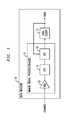
- FIG. 1is a high-level block diagram of a serial data receiver with CTE (Continuous Time Equalizer) and DFE (Decision Feedback Equalizer) processing functions.
- CTEContinuous Time Equalizer
- DFEDecision Feedback Equalizer
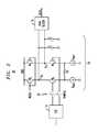
- FIG. 2is a schematic circuit diagram of a sampled current integrator circuit.
- FIG. 3is a high-level schematic diagram of a variable peaked current integrator circuit, according to an exemplary embodiment of the invention.
- FIG. 4is a schematic circuit diagram of a variable peaked current integrator circuit using variable capacitive degeneration to control a peaking response of the current integrator circuit, according to an exemplary embodiment of the invention.
- FIG. 5is a schematic circuit diagram of a variable peaked current integrator circuit using variable bias current control to adjust a peaking response of the current integrator circuit, according to another exemplary embodiment of the invention.
- FIG. 1is a high-level block diagram of a serial data receiver.
- a serial data receiver 10as depicted in FIG. 1 comprises an analog signal processing and equalizing circuit block 11 and a data slicer 12 , which operate to convert an analog signal received over a communications channel to digital values which represent estimates of the transmitted data.
- the analog signal processing and equalizing circuit block 11comprises a VGA (variable-gain amplifier) block 13 , a CTE (Continuous Time Equalizer) block 14 , and a DFE (Decision-Feedback Equalization) block 15 , which implement well known functions to process an incoming analog signal and provide line (channel) equalization functions to compensate degradation from line intersymbol interference (ISI).
- the data slicer block 12converts the equalized analog signal to binary data using well known techniques.
- ultra-high data rate (e.g., 10 to 25 Gb/s) receiversis the need to support a very wide bandwidth in the analog signal processing and equalizing circuit block 11 , while simultaneously keeping both the power draw and complexity of the analog circuitry as low as possible.
- a serial line receiver designed to operate with a 25 Gb/s incoming data ratetypically requires an analog bandwidth of at least 12.5 GHz, or half the data rate, to support non-return-to-zero (NRZ) line signaling.
- the analog signal processing and equalizing circuit block 11can implement high frequency peaking through the use of the CTE block 14 , to realize a frequency dependent gain which peaks at high frequency. This high frequency peaking extends the bandwidth of the receiver to more than half the data rate.
- High-frequency peakinghelps equalize the line, it can also increase noise arising from the active and passive components forming the receiver, as the high-frequency peaking simultaneously increases the noise bandwidth of the receiver.
- High data rate receiversare also susceptible to degradation from broad-band crosstalk noise arising from unwanted parasitic coupling from physically adjacent data channels. Exemplary embodiments of the invention as discussed in detail below provide signal processing frameworks to minimize the impact of both crosstalk noise and receiver circuit noise with high data rate receivers that operate over a wide bandwidth.
- a serial data receivermay be designed with a bandwidth that supports the highest data rate (e.g., 25 Gb/s), but the receiver must also operate with “legacy” data rates (e.g, 3 Gb/s).
- the high bandwidth of the high data rate receiver when used at lower data ratesresults in non-optimum SNR at the lower data rate.
- Exemplary embodiments of the invention as discussed in detail belowprovide signal processing frameworks to control receiver bandwidth as a function of data rate.
- FIG. 2is a schematic circuit diagram of a sampled current integrator circuit 20 comprising a CTE block 14 , a sampling block 22 (sampling switches), a current integrator circuit 24 and a data slicer block 12 .
- the current integrator circuit 24has a differential amplifier topology comprising a differential input stage formed by differential transistor pair M 0 and M 1 , and load elements including PMOS switches M 2 and M 3 that are driven by a clock signal RESET, and resettable capacitors C at each output node N 1 and N 2 .
- the capacitors Care connected between the output nodes N 1 and N 2 and ground.
- the gates of transistors M 0 and M 1are differential inputs that receive as input a differential input signal (voltage) from the sampling block 22 .
- the differential amplifierfurther comprises a degeneration resistor RD and two tail current sources I BIAS to generate a bias current for DC biasing the differential input amplifier.
- a signal typically coming from the CTE block 14 in a data receiver front-endis first sampled by the sampling block 22 , which samples the incoming signal and holds its state in response to a SAMPLE signal.
- the sampled value at the input of the current integrator circuit 24is integrated over a nominal data bit period T (or integration period) by releasing reset on the integrating load capacitors C with the RESET signal. More specifically, when the clock signal RESET is logic “low,” the current integrator circuit 24 is in reset mode, and the PMOS transistors M 2 and M 3 pull up the output nodes N 1 and N to the positive power supply voltage VDD.
- the PMOS transistors M 2 and M 3are turned off, the reset period ends, and the drain currents from the input differential pair (which is driven by inputs from the sampling block 22 ) begin to charge the load capacitors C.
- this “integration” periodcurrent is integrated by the capacitors C. With a nonzero differential input voltage, the drain currents from the input differential pair are unequal, so the load capacitors C charge at different rates.
- a positive or negative differential output voltageis developed, and the integrated output from the sampled current integrator block 22 / 24 is converted to data by the data slicer block 12 , which may be realized as a high sensitivity binary latch.
- An advantage of the sampled current integrator circuit topology of FIG. 2is its ability to easily add decision-feedback equalization through the use of additional switched current sources on the capacitive integrating node.
- the circuit topologyalso minimizes power and area—since the integrating capacitance C can be very small, it takes very small currents to develop sufficient differential output voltage to reliably drive the data slicer block 12 . Further, because the circuit integrates a held value, there is no bandwidth loss in the stage from the integration process itself.
- the sampled current integratoravoids integrator loss, there is still a loss in bandwidth arising from the sampling process due to the series resistance of samplers within the sampling block 22 combined with the load capacitance at the input of the current integrator. This loss increases at extremely high data rates due to practical limits on how small the series resistance of the samplers 22 and input capacitance of the integrating buffer can be made. Further, the sampling process inherently adds undesired kT/C noise of the sampler to the signal, degrading the SNR of the received signal.
- the sampling processcan also result in significant “kickback” to the stage driving the sampler input due to charge-redistribution from the “hold” capacitance at the output of the sampling block 22 back to its input when the sampling block 22 is re-configured from its “hold” state to its “track” state.
- This “kickback” effectcan result in the need for extra buffer circuitry preceding the sampling block 22 to reduce the “kickback” noise levels to other circuits (such as edge path samplers for use in clock recovery) which may be connected to the output of the CTE block 14 .
- the sampler kickback noisecan also degrade high data rate receiver sensitivity if the noise does decay to a sufficiently small level before the sampling block 22 is re-configured from its “track” state to its “hold” state.
- FIGS. 3 , 4 and 5provide peaked analog signal current integration topologies that leverage low power and silicon die area as realized by use of a current integrator in the analog signal processing data path, while eliminating bandwidth loss, kT/C noise degradation, and charge-redistribution kickback, which result from the sampling process in the sampled current integrator architecture of FIG. 2 .
- FIG. 3is a high-level schematic diagram of a variable peaked current integrator circuit, according to an exemplary embodiment of the invention. In general, FIG.
- FIG. 3depicts a high-level framework of a variable peaked current integrator circuit 30 comprising a transconductance amplifier 32 and a reset circuit 34 (which is controlled by a clock signal RESET), and a capacitor C connected to the output of the transconductance amplifier 32 .
- the transconductance amplifier 32is designed with a continuous-time adjustable peaking function Gm(f) to vary a peaking response of the current integrator circuit 30 in response to control signals generated by a peaking control module 36 .
- the current integrator circuit 30 of FIG. 3eliminates the sampling circuit at the input of transconductor 32 and implements an input transconductor with a continuous-time adjustable peaking function Gm(f) that is designed to compensate the inherent loss of direct (non-sampled) signal integration.
- Gm(f)a continuous-time adjustable peaking function
- An ideal current integratorwill attenuate a time-varying signal level by approximately 4 dB (relative to a DC input) at a frequency equal to 1/(2*T), where T is the integration period which normally corresponds to the bit period in a received NRZ data signal.
- the excess lossadds intersymbol interference to the signal and reduces the amount of external line loss that the receiver equalization system can handle.
- the exemplary framework of FIG. 3addresses these issues by employing a data-rate dependent variable peaking function, which can be used to not only restore the 4 dB integrator loss, but also adjust the peaking to help compensate other losses in the end-to-end channel.
- the peaking functioncan be adjusted as a function of the integration period T, which in turn is directly related to the operating data rate bit period. More specifically, in the exemplary embodiment of FIG. 3 , the peaking control module 36 can receive as input, configuration data indicative of the operating data rate or of a desired equalization control, and/or optionally an additional direct peaking control adjust, to configure a peaking level in the integrating stage of the transconductor 32 to a desired level across a wide data rate range of operation.
- the peaking control functionprovides a peaking control to compensate the inherent 4 dB loss of the integrator only, to provide a net “flat” frequency response in the integrator stage independent of operating data rate.
- the peaking control functionmay be augmented with control from an equalization control process, which further adjusts the peaking control in the integrator stage to achieve improved line equalization.
- a peaked current integrator architecture according to principles of the inventioninherently provides an effective data detection bandwidth which is closely matched to the data rate of operation, independent of PVT corner.
- a peaked current integrator architectureaddresses the problem of excess receiver circuit and system crosstalk noise which can occur either on a wide-band PVT corner, or when operating at a low data rate with a broad-band receiver.
- the detection bandwidth stabilizationoccurs due to the predictable loss (4 dB) resulting from the integration process at a frequency of 1/(2*T). Compensating this loss through a peaking function of a peaked current integrator architecture according to principles of the invention increases the bandwidth of the integrating stage, but because this compensation is a relatively small amount, the bandwidth variation of the entire receiver over PVT corners is reduced.
- a current integrator according to the inventionproduces a zero output independent of the setting of the peaking function, thereby realizing the goal of eliminating as much noise as possible while maintaining desired signal level equalization.
- the peaking function Gm(f) of the transconductor of FIG. 3is realized by employing a variable degeneration capacitor in a current integrating differential amplifier stage, such as shown in FIG. 4 .
- FIG. 4is a schematic circuit diagram of a variable peaked current integrator circuit 40 using variable capacitive degeneration to control a peaking response of the current integrator circuit, according to an exemplary embodiment of the invention.
- the circuit 40comprises an input amplifier stage 42 formed by differential transistor pair M 0 and M 1 , and further comprising a degeneration resistor RD and a variable degeneration capacitor CD forming a degeneration network, as well as tail current sources I 0 and I 1 providing DC current for DC biasing the input amplifier stage 42 .
- the gates of the input transistors M 0 and M 1are differential inputs that receive as input a differential voltage Vin from a CTE block 14 .
- the drains of transistors M 0 and M 1are connected to output nodes N 1 and N 2 .
- the circuit 40further comprises a reset circuit 44 comprising PMOS switches M 2 and M 3 that are driven by a clock signal RESET.
- the PMOS switches M 2 and M 3are connected to resettable capacitors C at each output node N 1 and N 2 .
- the capacitors Care connected between the output nodes N 1 and N 2 and ground.
- a differential signal output from the CTE block 14 in a data receiver front-endis directly input to the differential inputs of the input amplifier stage 42 (transistors M 0 /M 1 ).
- the input signal at the input to the current integrator circuit 40is integrated over a nominal data bit period T (integration period) by releasing reset on the integrating load capacitors C with the RESET signal. More specifically, when the clock signal RESET is logic “low,” the integrator 40 is in reset mode, and the PMOS transistors M 2 and M 3 pull up the output nodes N 1 and N to the positive power supply voltage VDD.
- the PMOS transistors M 2 and M 3are turned off, the reset period ends, and the drain currents from the input differential pair (which is directly driven by inputs from the CTE circuit 24 ) begin to charge the load capacitors C.
- this “integration” periodor data detection period
- currentis integrated by the capacitors C.
- the drain currents of the input differential pairare unequal, so the capacitors C charge at different rates.
- a positive or negative differential output voltageis developed at the output of the peaked current integrator circuit 40 , and the output is converted to data by the data slicer block 12 , which may be realized as a high sensitivity binary latch.
- the use of the degeneration resistor RDprovides a more linear, lower distortion response characteristic, which is desirable for analog applications.
- the variable degeneration capacitance CD in parallel with the degeneration resistor RDis utilized to introduce a “zero” in the frequency response, so that the high-frequency gain is higher than the DC gain at a desired peaking frequency.
- the degeneration capacitor CDessentially shorts out the degeneration resistor RD resulting in a higher gain (and lower loss).
- the amount of peaking(how much the high-frequency gain is boosted relative to the DC gain) can be adjusted by varying the degeneration capacitance CD in the degeneration network in response to control signals output from a peaking control module 46 .
- variable degeneration capacitor CDcan be implemented by employing a plurality of switches to connect different discrete capacitance values in parallel with the shunt degeneration resistor RD using techniques well established in the art.
- the number of parallel-connected discrete capacitors that are implementedwill depend on the amount of unit resolution that is desired for adjusting the value of the degeneration capacitance CD and the desired range of data rates for which the current integrating circuit will be operated.
- the peaking response of the peaked current integrator circuit 40 of FIG. 4can be dynamically adjusted as a function of real-time operating conditions such as the operating data rate and/or channel characteristics (adaptive equalization).
- configuration datacan be input to the peaking control module 46 which specifies the data rate of operation, and the peaking control module 46 will generate a control signal to set the value of the degeneration capacitor CD based on the specified data rate.
- equalization adjustment data(generated, for example, in real-time by some external equalization control processing circuit) can be input to the peaking control module 46 to vary the value of the degeneration capacitor CD (about the initially set degeneration capacitance value selected for the given data rate) to further tune the peaking response of the peaked current integrator circuit 40 to account for channel equalization.
- FIG. 5is a schematic circuit diagram of a variable peaked current integrator circuit using variable bias current control to adjust a peaking response of the current integrator circuit, according to another exemplary embodiment of the invention.
- the peaking function Gm(f)is realized using a parallel connection of two differential input amplifiers, one with a fixed degeneration resistor (and optional shunt degeneration capacitor) and another with only a shunt degeneration capacitor, wherein high frequency peaking is controlled by varying a tail bias current ratio between the resistor degenerated amplifier and the capacitor-only degenerated amplifier.
- a variable peaked current integrator circuit 50 as shown in FIG. 5comprises a first input amplifier stage 52 formed by differential transistor pair M 0 and M 1 , and further comprising a degeneration resistor RD and an optional fixed degeneration capacitor CD 1 forming a degeneration network, as well as adjustable tail current sources 58 A and 58 B providing an adjustable DC current for DC biasing the first input amplifier stage 52 .
- the gates of the input transistors M 0 and M 1are differential inputs that receive as input a differential voltage Vin from the CTE block 14 .
- the drains of transistors M 0 and M 1are connected to output nodes N 1 and N 2 .
- the circuit 50further comprises a reset circuit 54 comprising PMOS switches M 2 and M 3 that are driven by a clock signal RESET, and resettable capacitors C at each output node N 1 and N 2 .
- the capacitors Care connected between the output nodes N 1 and N 2 and ground.
- the variable peaked current integrator circuit 50further comprises a second input amplifier stage 53 formed by differential transistor pair M 4 and M 5 , and further comprising a fixed degeneration capacitor CD 2 providing capacitive degeneration for the second input amplifier stage 53 , as, well as adjustable tail current sources 58 C and 58 D providing an adjustable DC current for DC biasing the second input amplifier stage 53 .
- the gates of the input transistors M 4 and M 5are differential inputs that are commonly connected to the gates of input transistors M 0 and M 1 , respectively, and receive the same differential voltage Vin from the CTE block 14 .
- the drains of transistors M 4 and M 5 of the second input amplifier stage 53are also connected to the output nodes N 1 and N 2 , respectively.
- the amount of peakingcan be adjusted by varying the amount of bias currents generated by the tail current sources 58 in response to control signals output from a peaking control module 56 .
- a high frequency peaking responsecan be controlled by varying a ratio between the tail bias currents of the adjustable current sources 58 A/ 58 B of the first (resistor degenerated) input amplifier stage 52 and the tail bias currents of the adjustable current sources 58 C/ 58 D of the second (capacitor-only degenerated) input amplifier stage 53 .
- the adjustable tail current sourcescan be implemented using common current DACs that are constructed using techniques well known in the art.
- peaked current integrating amplifierswhich can be utilized in integrated circuit chips with various analog and digital integrated circuitries.
- integrated circuit diescan be fabricated having peaked current integrating amplifiers and other semiconductor devices such as field-effect transistors, bipolar transistors, metal-oxide-semiconductor transistors, diodes, resistors, capacitors, inductors, etc., forming analog and/or digital circuits.
- the peaked current integrating amplifierscan be formed upon or within a semiconductor substrate, the die also comprising the substrate.
- An integrated circuit in accordance with the present inventioncan be employed in applications, hardware, and/or electronic systems.
- Suitable hardware and systems for implementing the inventionmay include, but are not limited to, personal computers, communication networks, electronic commerce systems, portable communications devices (e.g., cell phones), solid-state media storage devices, functional circuitry, etc. Systems and hardware incorporating such integrated circuits are considered part of this invention. Given the teachings of the invention provided herein, one of ordinary skill in the art will be able to contemplate other implementations and applications of the techniques of the invention.
Landscapes
- Engineering & Computer Science (AREA)
- Physics & Mathematics (AREA)
- Power Engineering (AREA)
- Mathematical Physics (AREA)
- Theoretical Computer Science (AREA)
- Computer Networks & Wireless Communication (AREA)
- Signal Processing (AREA)
- Software Systems (AREA)
- Computer Hardware Design (AREA)
- General Physics & Mathematics (AREA)
- Amplifiers (AREA)
Abstract
Description
Claims (20)
Priority Applications (2)
| Application Number | Priority Date | Filing Date | Title |
|---|---|---|---|
| US13/399,675US8964825B2 (en) | 2012-02-17 | 2012-02-17 | Analog signal current integrators with tunable peaking function |
| CN201310045932.3ACN103259508B (en) | 2012-02-17 | 2013-02-05 | There is the analog signal current integrator of adjustable peaking function |
Applications Claiming Priority (1)
| Application Number | Priority Date | Filing Date | Title |
|---|---|---|---|
| US13/399,675US8964825B2 (en) | 2012-02-17 | 2012-02-17 | Analog signal current integrators with tunable peaking function |
Publications (2)
| Publication Number | Publication Date |
|---|---|
| US20130215954A1 US20130215954A1 (en) | 2013-08-22 |
| US8964825B2true US8964825B2 (en) | 2015-02-24 |
Family
ID=48963248
Family Applications (1)
| Application Number | Title | Priority Date | Filing Date |
|---|---|---|---|
| US13/399,675Active2033-06-02US8964825B2 (en) | 2012-02-17 | 2012-02-17 | Analog signal current integrators with tunable peaking function |
Country Status (2)
| Country | Link |
|---|---|
| US (1) | US8964825B2 (en) |
| CN (1) | CN103259508B (en) |
Cited By (6)
| Publication number | Priority date | Publication date | Assignee | Title |
|---|---|---|---|---|
| US9425999B1 (en)* | 2015-09-30 | 2016-08-23 | Synaptics Incorporated | Process-voltage-temperature (PVT) invariant continuous time equalizer |
| US9954495B1 (en) | 2016-10-24 | 2018-04-24 | Synaptics Incorporated | PVT invariant peaking stage for continuous time linear equalizer |
| US10686643B1 (en) | 2019-03-04 | 2020-06-16 | International Business Machines Corporation | Discrete time analog front end circuit implemented in a receiver device |
| US10992277B1 (en)* | 2019-12-06 | 2021-04-27 | Qualcomm Incorporated | Variable gain amplifier with embedded equalization for uniform tuning |
| US11469729B2 (en)* | 2019-06-11 | 2022-10-11 | Mediatek Singapore Pte. Ltd. | Hybrid receiver front-end |
| TWI865040B (en)* | 2023-06-26 | 2024-12-01 | 旺宏電子股份有限公司 | Electronic circuit, memory device and method for compensating for data distortion from channel loss |
Families Citing this family (58)
| Publication number | Priority date | Publication date | Assignee | Title |
|---|---|---|---|---|
| US9251873B1 (en) | 2010-05-20 | 2016-02-02 | Kandou Labs, S.A. | Methods and systems for pin-efficient memory controller interface using vector signaling codes for chip-to-chip communications |
| US9077386B1 (en) | 2010-05-20 | 2015-07-07 | Kandou Labs, S.A. | Methods and systems for selection of unions of vector signaling codes for power and pin efficient chip-to-chip communication |
| US9288082B1 (en) | 2010-05-20 | 2016-03-15 | Kandou Labs, S.A. | Circuits for efficient detection of vector signaling codes for chip-to-chip communication using sums of differences |
| US8810319B1 (en)* | 2012-06-08 | 2014-08-19 | Altera Corporation | Dual-stage continuous-time linear equalizer |
| US8643422B1 (en)* | 2012-07-12 | 2014-02-04 | Taiwan Semiconductor Manufacturing Company, Ltd. | Slicer and method of operating the same |
| CN110166217B (en) | 2013-04-16 | 2022-05-17 | 康杜实验室公司 | High bandwidth communication interface method and system |
| EP2997704B1 (en) | 2013-06-25 | 2020-12-16 | Kandou Labs S.A. | Vector signaling with reduced receiver complexity |
| US9806761B1 (en) | 2014-01-31 | 2017-10-31 | Kandou Labs, S.A. | Methods and systems for reduction of nearest-neighbor crosstalk |
| US9100232B1 (en) | 2014-02-02 | 2015-08-04 | Kandou Labs, S.A. | Method for code evaluation using ISI ratio |
| KR102240544B1 (en) | 2014-02-28 | 2021-04-19 | 칸도우 랩스 에스에이 | Clock-embedded vector signaling codes |
| US9509437B2 (en) | 2014-05-13 | 2016-11-29 | Kandou Labs, S.A. | Vector signaling code with improved noise margin |
| US9112550B1 (en) | 2014-06-25 | 2015-08-18 | Kandou Labs, SA | Multilevel driver for high speed chip-to-chip communications |
| EP3138253A4 (en) | 2014-07-10 | 2018-01-10 | Kandou Labs S.A. | Vector signaling codes with increased signal to noise characteristics |
| KR101943048B1 (en) | 2014-07-21 | 2019-01-28 | 칸도우 랩스 에스에이 | Multidrop data transfer |
| WO2016019384A1 (en) | 2014-08-01 | 2016-02-04 | Kandou Labs, S.A. | Orthogonal differential vector signaling codes with embedded clock |
| US9674014B2 (en) | 2014-10-22 | 2017-06-06 | Kandou Labs, S.A. | Method and apparatus for high speed chip-to-chip communications |
| KR101978470B1 (en) | 2015-06-26 | 2019-05-14 | 칸도우 랩스 에스에이 | High-speed communication system |
| US10116470B2 (en)* | 2015-10-28 | 2018-10-30 | Futurewei Technologies, Inc. | Combined low and high frequency continuous-time linear equalizers |
| US10055372B2 (en) | 2015-11-25 | 2018-08-21 | Kandou Labs, S.A. | Orthogonal differential vector signaling codes with embedded clock |
| US10003315B2 (en) | 2016-01-25 | 2018-06-19 | Kandou Labs S.A. | Voltage sampler driver with enhanced high-frequency gain |
| US10242749B2 (en) | 2016-04-22 | 2019-03-26 | Kandou Labs, S.A. | Calibration apparatus and method for sampler with adjustable high frequency gain |
| US10003454B2 (en) | 2016-04-22 | 2018-06-19 | Kandou Labs, S.A. | Sampler with low input kickback |
| US10193716B2 (en) | 2016-04-28 | 2019-01-29 | Kandou Labs, S.A. | Clock data recovery with decision feedback equalization |
| US10153591B2 (en) | 2016-04-28 | 2018-12-11 | Kandou Labs, S.A. | Skew-resistant multi-wire channel |
| EP3449379B1 (en) | 2016-04-28 | 2021-10-06 | Kandou Labs S.A. | Vector signaling codes for densely-routed wire groups |
| US9906358B1 (en) | 2016-08-31 | 2018-02-27 | Kandou Labs, S.A. | Lock detector for phase lock loop |
| US10411922B2 (en) | 2016-09-16 | 2019-09-10 | Kandou Labs, S.A. | Data-driven phase detector element for phase locked loops |
| US10200188B2 (en) | 2016-10-21 | 2019-02-05 | Kandou Labs, S.A. | Quadrature and duty cycle error correction in matrix phase lock loop |
| US10200218B2 (en) | 2016-10-24 | 2019-02-05 | Kandou Labs, S.A. | Multi-stage sampler with increased gain |
| US10372665B2 (en) | 2016-10-24 | 2019-08-06 | Kandou Labs, S.A. | Multiphase data receiver with distributed DFE |
| WO2018217786A1 (en)* | 2017-05-22 | 2018-11-29 | Kandou Labs, S.A. | Multi-stage sampler with increased gain |
| US10116468B1 (en) | 2017-06-28 | 2018-10-30 | Kandou Labs, S.A. | Low power chip-to-chip bidirectional communications |
| US10686583B2 (en) | 2017-07-04 | 2020-06-16 | Kandou Labs, S.A. | Method for measuring and correcting multi-wire skew |
| US10203226B1 (en) | 2017-08-11 | 2019-02-12 | Kandou Labs, S.A. | Phase interpolation circuit |
| EP3477863B1 (en)* | 2017-08-30 | 2022-05-04 | Shenzhen Goodix Technology Co., Ltd. | Dynamic amplifying circuit |
| US10326623B1 (en) | 2017-12-08 | 2019-06-18 | Kandou Labs, S.A. | Methods and systems for providing multi-stage distributed decision feedback equalization |
| US10554380B2 (en) | 2018-01-26 | 2020-02-04 | Kandou Labs, S.A. | Dynamically weighted exclusive or gate having weighted output segments for phase detection and phase interpolation |
| US10931249B2 (en) | 2018-06-12 | 2021-02-23 | Kandou Labs, S.A. | Amplifier with adjustable high-frequency gain using varactor diodes |
| KR102707165B1 (en) | 2018-06-12 | 2024-09-13 | 칸도우 랩스 에스에이 | Passive multi-input comparator for orthogonal codes on multi-wire buses |
| CN109302147A (en)* | 2018-08-31 | 2019-02-01 | 光梓信息科技(上海)有限公司 | A kind of decision feedback equalizer, decision-feedback system and its decision-feedback method |
| US11183983B2 (en) | 2018-09-10 | 2021-11-23 | Kandou Labs, S.A. | Programmable continuous time linear equalizer having stabilized high-frequency peaking for controlling operating current of a slicer |
| US10447507B1 (en)* | 2018-10-26 | 2019-10-15 | Nxp B.V. | Low supply linear equalizer with programmable peaking gain |
| CN113396478B (en)* | 2019-03-22 | 2023-01-06 | 华为技术有限公司 | Equalization circuit, packaging device and data transmission device |
| US10721106B1 (en) | 2019-04-08 | 2020-07-21 | Kandou Labs, S.A. | Adaptive continuous time linear equalization and channel bandwidth control |
| US10680634B1 (en) | 2019-04-08 | 2020-06-09 | Kandou Labs, S.A. | Dynamic integration time adjustment of a clocked data sampler using a static analog calibration circuit |
| US10608849B1 (en) | 2019-04-08 | 2020-03-31 | Kandou Labs, S.A. | Variable gain amplifier and sampler offset calibration without clock recovery |
| US10574487B1 (en) | 2019-04-08 | 2020-02-25 | Kandou Labs, S.A. | Sampler offset calibration during operation |
| US11271783B2 (en)* | 2020-02-26 | 2022-03-08 | Taiwan Semiconductor Manufacturing Co., Ltd. | Decision feedback equalization embedded in a slicer |
| US11228470B2 (en) | 2020-05-18 | 2022-01-18 | Nxp B.V. | Continuous time linear equalization circuit |
| US11206160B2 (en)* | 2020-05-18 | 2021-12-21 | Nxp B.V. | High bandwidth continuous time linear equalization circuit |
| WO2022018824A1 (en)* | 2020-07-21 | 2022-01-27 | 日本電信電話株式会社 | Amplifier circuit and driver circuit |
| US11303484B1 (en) | 2021-04-02 | 2022-04-12 | Kandou Labs SA | Continuous time linear equalization and bandwidth adaptation using asynchronous sampling |
| US11374800B1 (en) | 2021-04-14 | 2022-06-28 | Kandou Labs SA | Continuous time linear equalization and bandwidth adaptation using peak detector |
| US11456708B1 (en) | 2021-04-30 | 2022-09-27 | Kandou Labs SA | Reference generation circuit for maintaining temperature-tracked linearity in amplifier with adjustable high-frequency gain |
| CN113206810B (en)* | 2021-07-05 | 2021-09-17 | 牛芯半导体(深圳)有限公司 | Adjustable equalizer and adjusting method |
| US12355409B2 (en) | 2022-03-24 | 2025-07-08 | Kandou Labs SA | Variable gain amplifier with cross-coupled common mode reduction |
| CN116243755B (en)* | 2023-05-09 | 2023-07-25 | 国仪量子(合肥)技术有限公司 | Data acquisition device and data acquisition and monitoring system |
| CN119363097A (en)* | 2024-12-23 | 2025-01-24 | 上海晟联科半导体有限公司 | Single-ended to differential signal conversion circuit and method |
Citations (9)
| Publication number | Priority date | Publication date | Assignee | Title |
|---|---|---|---|---|
| US5377272A (en) | 1992-08-28 | 1994-12-27 | Thomson Consumer Electronics, Inc. | Switched signal processing circuit |
| US20010053174A1 (en) | 1994-07-22 | 2001-12-20 | Aether Wire & Location | Spread spectrum localizers |
| US20060182171A1 (en)* | 2005-02-04 | 2006-08-17 | Maarten Kuijk | Multistage tuning-tolerant equalizer filter |
| US20070057722A1 (en)* | 2002-02-01 | 2007-03-15 | Youngwoo Kwon | Power amplification apparatus of a portable terminal |
| CN101271142A (en) | 2007-03-21 | 2008-09-24 | 中国科学院电子学研究所 | Peak detection circuit integrated on CMOS single chip |
| US20100046683A1 (en)* | 2008-08-20 | 2010-02-25 | Troy James Beukema | Adaptive clock and equalization control systems and methods for data receivers in communications systems |
| US8031763B2 (en)* | 2006-12-28 | 2011-10-04 | Intel Corporation | Automatic tuning circuit for a continuous-time equalizer |
| US8085841B2 (en) | 2008-04-02 | 2011-12-27 | International Business Machines Corporation | Sampled current-integrating decision feedback equalizer and method |
| US20120176667A1 (en)* | 2009-09-25 | 2012-07-12 | Zte Corporation | Method and Apparatus for Amplifying and Dynamically Adjusting Optical Signal |
Family Cites Families (3)
| Publication number | Priority date | Publication date | Assignee | Title |
|---|---|---|---|---|
| JP3293576B2 (en)* | 1998-12-09 | 2002-06-17 | 日本電気株式会社 | Peak hold circuit |
| US7792185B2 (en)* | 2007-02-07 | 2010-09-07 | International Business Machines Corporation | Methods and apparatus for calibrating output voltage levels associated with current-integrating summing amplifier |
| CN201663584U (en)* | 2010-04-06 | 2010-12-01 | 四川和芯微电子股份有限公司 | Front-loading balancing and amplifying circuit |
- 2012
- 2012-02-17USUS13/399,675patent/US8964825B2/enactiveActive
- 2013
- 2013-02-05CNCN201310045932.3Apatent/CN103259508B/enactiveActive
Patent Citations (9)
| Publication number | Priority date | Publication date | Assignee | Title |
|---|---|---|---|---|
| US5377272A (en) | 1992-08-28 | 1994-12-27 | Thomson Consumer Electronics, Inc. | Switched signal processing circuit |
| US20010053174A1 (en) | 1994-07-22 | 2001-12-20 | Aether Wire & Location | Spread spectrum localizers |
| US20070057722A1 (en)* | 2002-02-01 | 2007-03-15 | Youngwoo Kwon | Power amplification apparatus of a portable terminal |
| US20060182171A1 (en)* | 2005-02-04 | 2006-08-17 | Maarten Kuijk | Multistage tuning-tolerant equalizer filter |
| US8031763B2 (en)* | 2006-12-28 | 2011-10-04 | Intel Corporation | Automatic tuning circuit for a continuous-time equalizer |
| CN101271142A (en) | 2007-03-21 | 2008-09-24 | 中国科学院电子学研究所 | Peak detection circuit integrated on CMOS single chip |
| US8085841B2 (en) | 2008-04-02 | 2011-12-27 | International Business Machines Corporation | Sampled current-integrating decision feedback equalizer and method |
| US20100046683A1 (en)* | 2008-08-20 | 2010-02-25 | Troy James Beukema | Adaptive clock and equalization control systems and methods for data receivers in communications systems |
| US20120176667A1 (en)* | 2009-09-25 | 2012-07-12 | Zte Corporation | Method and Apparatus for Amplifying and Dynamically Adjusting Optical Signal |
Cited By (7)
| Publication number | Priority date | Publication date | Assignee | Title |
|---|---|---|---|---|
| US9425999B1 (en)* | 2015-09-30 | 2016-08-23 | Synaptics Incorporated | Process-voltage-temperature (PVT) invariant continuous time equalizer |
| US9954495B1 (en) | 2016-10-24 | 2018-04-24 | Synaptics Incorporated | PVT invariant peaking stage for continuous time linear equalizer |
| US10686643B1 (en) | 2019-03-04 | 2020-06-16 | International Business Machines Corporation | Discrete time analog front end circuit implemented in a receiver device |
| US11469729B2 (en)* | 2019-06-11 | 2022-10-11 | Mediatek Singapore Pte. Ltd. | Hybrid receiver front-end |
| US10992277B1 (en)* | 2019-12-06 | 2021-04-27 | Qualcomm Incorporated | Variable gain amplifier with embedded equalization for uniform tuning |
| TWI865040B (en)* | 2023-06-26 | 2024-12-01 | 旺宏電子股份有限公司 | Electronic circuit, memory device and method for compensating for data distortion from channel loss |
| US12308049B2 (en) | 2023-06-26 | 2025-05-20 | Macronix International Co., Ltd. | Decision feedback equalization in semiconductor devices |
Also Published As
| Publication number | Publication date |
|---|---|
| US20130215954A1 (en) | 2013-08-22 |
| CN103259508B (en) | 2016-09-07 |
| CN103259508A (en) | 2013-08-21 |
Similar Documents
| Publication | Publication Date | Title |
|---|---|---|
| US8964825B2 (en) | Analog signal current integrators with tunable peaking function | |
| US10313165B2 (en) | Finite impulse response analog receive filter with amplifier-based delay chain | |
| US8558611B2 (en) | Peaking amplifier with capacitively-coupled parallel input stages | |
| US8755428B2 (en) | Feed-forward equalizer architectures | |
| Sun et al. | A low-power, 20-Gb/s continuous-time adaptive passive equalizer | |
| US8200179B1 (en) | Combined variable gain amplifier and analog equalizer circuit | |
| EP2878079B1 (en) | Receiver having a wide common mode input range | |
| US8588289B2 (en) | Adaptive signal equalizer with segmented coarse and fine controls | |
| US6937054B2 (en) | Programmable peaking receiver and method | |
| US20070133671A1 (en) | Active delay line | |
| JP2019507552A (en) | Auto gain control circuit interleaved with linear gain sign | |
| CN114337732B (en) | Low power receiver with equalization circuit, communication unit and method thereof | |
| US9059874B2 (en) | Switched continuous time linear equalizer with integrated sampler | |
| US9973356B1 (en) | Slicer and decision feedback equalization circuitry | |
| CN213461678U (en) | Continuous time linear equalizer | |
| US10797658B1 (en) | Low power optical link | |
| US7969218B2 (en) | Receiver for reducing intersymbol interference of a channel and compensating for signal gain loss, and method thereof | |
| US7695085B2 (en) | Variable gain amplifier having variable gain DC offset loop | |
| US8907729B2 (en) | Trans-impedance amplifier for high speed optical-electrical interfaces | |
| CN112073077B (en) | Receiver front-end | |
| US7656939B2 (en) | Adaptive equalizer with passive and active stages | |
| US10833898B2 (en) | Baseline wander correction in AC coupled communication links using equalizer with active feedback | |
| US20170373761A1 (en) | Apparatus and method for recovering data at an optical receiver with automatic tuning | |
| Yu et al. | 56 Gb/s PAM-4 optical receiver frontend in an advanced FinFET process | |
| US20030218502A1 (en) | Variable gain amplifier |
Legal Events
| Date | Code | Title | Description |
|---|---|---|---|
| AS | Assignment | Owner name:INTERNATIONAL BUSINESS MACHINES CORPORATION, NEW Y Free format text:ASSIGNMENT OF ASSIGNORS INTEREST;ASSIGNORS:BEUKEMA, TROY J.;BULZACCHELLI, JOHN F.;SIGNING DATES FROM 20120221 TO 20120305;REEL/FRAME:027915/0446 | |
| STCF | Information on status: patent grant | Free format text:PATENTED CASE | |
| AS | Assignment | Owner name:GLOBALFOUNDRIES U.S. 2 LLC, NEW YORK Free format text:ASSIGNMENT OF ASSIGNORS INTEREST;ASSIGNOR:INTERNATIONAL BUSINESS MACHINES CORPORATION;REEL/FRAME:036550/0001 Effective date:20150629 | |
| AS | Assignment | Owner name:GLOBALFOUNDRIES INC., CAYMAN ISLANDS Free format text:ASSIGNMENT OF ASSIGNORS INTEREST;ASSIGNORS:GLOBALFOUNDRIES U.S. 2 LLC;GLOBALFOUNDRIES U.S. INC.;REEL/FRAME:036779/0001 Effective date:20150910 | |
| MAFP | Maintenance fee payment | Free format text:PAYMENT OF MAINTENANCE FEE, 4TH YEAR, LARGE ENTITY (ORIGINAL EVENT CODE: M1551) Year of fee payment:4 | |
| AS | Assignment | Owner name:WILMINGTON TRUST, NATIONAL ASSOCIATION, DELAWARE Free format text:SECURITY AGREEMENT;ASSIGNOR:GLOBALFOUNDRIES INC.;REEL/FRAME:049490/0001 Effective date:20181127 | |
| AS | Assignment | Owner name:GLOBALFOUNDRIES U.S. INC., CALIFORNIA Free format text:ASSIGNMENT OF ASSIGNORS INTEREST;ASSIGNOR:GLOBALFOUNDRIES INC.;REEL/FRAME:054633/0001 Effective date:20201022 | |
| AS | Assignment | Owner name:GLOBALFOUNDRIES INC., CAYMAN ISLANDS Free format text:RELEASE BY SECURED PARTY;ASSIGNOR:WILMINGTON TRUST, NATIONAL ASSOCIATION;REEL/FRAME:054636/0001 Effective date:20201117 | |
| AS | Assignment | Owner name:GLOBALFOUNDRIES U.S. INC., NEW YORK Free format text:RELEASE BY SECURED PARTY;ASSIGNOR:WILMINGTON TRUST, NATIONAL ASSOCIATION;REEL/FRAME:056987/0001 Effective date:20201117 | |
| MAFP | Maintenance fee payment | Free format text:PAYMENT OF MAINTENANCE FEE, 8TH YEAR, LARGE ENTITY (ORIGINAL EVENT CODE: M1552); ENTITY STATUS OF PATENT OWNER: LARGE ENTITY Year of fee payment:8 |