US8964474B2 - Architecture for 3-D NAND memory - Google Patents
Architecture for 3-D NAND memoryDownload PDFInfo
- Publication number
- US8964474B2 US8964474B2US13/524,872US201213524872AUS8964474B2US 8964474 B2US8964474 B2US 8964474B2US 201213524872 AUS201213524872 AUS 201213524872AUS 8964474 B2US8964474 B2US 8964474B2
- Authority
- US
- United States
- Prior art keywords
- memory cell
- array
- data
- coupled
- strings
- Prior art date
- Legal status (The legal status is an assumption and is not a legal conclusion. Google has not performed a legal analysis and makes no representation as to the accuracy of the status listed.)
- Active, expires
Links
- 230000015654memoryEffects0.000titleclaimsabstractdescription354
- 238000003491arrayMethods0.000claimsabstractdescription135
- 238000000034methodMethods0.000claimsabstractdescription19
- 230000002401inhibitory effectEffects0.000claims3
- 239000004065semiconductorSubstances0.000abstractdescription9
- 238000010586diagramMethods0.000description31
- 239000000758substrateSubstances0.000description8
- 230000008878couplingEffects0.000description6
- 238000010168coupling processMethods0.000description6
- 238000005859coupling reactionMethods0.000description6
- 238000004519manufacturing processMethods0.000description3
- 238000012545processingMethods0.000description2
- 230000006978adaptationEffects0.000description1
- 238000013508migrationMethods0.000description1
- 230000005012migrationEffects0.000description1
- 230000002093peripheral effectEffects0.000description1
- 229910000679solderInorganic materials0.000description1
- 238000012546transferMethods0.000description1
Images


Classifications
- G—PHYSICS
- G11—INFORMATION STORAGE
- G11C—STATIC STORES
- G11C16/00—Erasable programmable read-only memories
- G11C16/02—Erasable programmable read-only memories electrically programmable
- G11C16/04—Erasable programmable read-only memories electrically programmable using variable threshold transistors, e.g. FAMOS
- G11C16/0483—Erasable programmable read-only memories electrically programmable using variable threshold transistors, e.g. FAMOS comprising cells having several storage transistors connected in series
- G—PHYSICS
- G11—INFORMATION STORAGE
- G11C—STATIC STORES
- G11C16/00—Erasable programmable read-only memories
- G11C16/02—Erasable programmable read-only memories electrically programmable
- G11C16/06—Auxiliary circuits, e.g. for writing into memory
- G—PHYSICS
- G11—INFORMATION STORAGE
- G11C—STATIC STORES
- G11C16/00—Erasable programmable read-only memories
- G11C16/02—Erasable programmable read-only memories electrically programmable
- G11C16/06—Auxiliary circuits, e.g. for writing into memory
- G11C16/34—Determination of programming status, e.g. threshold voltage, overprogramming or underprogramming, retention
- G11C16/3418—Disturbance prevention or evaluation; Refreshing of disturbed memory data
- G11C16/3427—Circuits or methods to prevent or reduce disturbance of the state of a memory cell when neighbouring cells are read or written
- G—PHYSICS
- G11—INFORMATION STORAGE
- G11C—STATIC STORES
- G11C2213/00—Indexing scheme relating to G11C13/00 for features not covered by this group
- G11C2213/70—Resistive array aspects
- G11C2213/71—Three dimensional array
Definitions
- Memory devicessuch as flash memory, are widely used in computers and electronic products. Such memory devices usually have a memory array with numerous memory cells to store information. These memory devices also have circuitry to transfer information to and from the memory array. Information can be stored into the memory cells in a programming operation. The stored information can be retrieved in a read operation or can be cleared in an erase operation. In semiconductor memories, there is continuous pressure to reduce component dimensions and fit more components in a given amount of chip area. As dimensions shrink, various technical hurdles become more significant.
- FIG. 1shows a block diagram of a memory device according to an embodiment of the invention.
- FIG. 2shows a schematic diagram of a memory string device example according to an embodiment of the invention.
- FIG. 3shows an isometric block diagram of a memory device according to an embodiment of the invention.
- FIG. 4shows a schematic diagram of the memory device from FIG. 3 according to an embodiment of the invention.
- FIG. 5shows an isometric block diagram of a memory device according to an embodiment of the invention.
- FIG. 6shows a schematic diagram of the memory device from FIG. 5 according to an embodiment of the invention.
- FIG. 7shows an isometric block diagram of a memory device according to an embodiment of the invention.
- FIG. 8shows a schematic diagram of the memory device from FIG. 7 according to an embodiment of the invention.
- FIG. 9shows an isometric block diagram of a memory device according to an embodiment of the invention.
- FIG. 10shows a schematic diagram of the memory device from FIG. 9 according to an embodiment of the invention.
- FIG. 11shows an isometric block diagram of a memory device according to an embodiment of the invention.
- FIG. 12shows a schematic diagram of the memory device from FIG. 11 according to an embodiment of the invention.
- FIG. 13shows a schematic diagram of a memory device according to an embodiment of the invention.
- FIG. 14shows an isometric block diagram of a memory device according to an embodiment of the invention.
- FIG. 15shows a schematic diagram of the memory device from FIG. 14 according to an embodiment of the invention.
- FIG. 16shows an isometric block diagram of a memory device according to an embodiment of the invention.
- FIG. 17shows a schematic diagram of the memory device from FIG. 16 according to an embodiment of the invention.
- FIG. 18shows a flow diagram of an example method according to an embodiment of the invention.
- FIG. 19shows a flow diagram of an example method according to an embodiment of the invention.
- FIG. 20shows a flow diagram of an example method according to an embodiment of the invention.
- FIG. 21shows an information handling system, including a memory device according to an embodiment of the invention.
- horizontalas used in this application is defined as a plane parallel to the conventional plane or surface of a wafer or substrate, regardless of the orientation of the wafer or substrate.
- verticalrefers to a direction perpendicular to the horizontal as defined above. Prepositions, such as “on,” “side” (as in “sidewall”), “higher,” “lower,” “over,” and “under” are defined with respect to the conventional plane or surface being on the top surface of the wafer or substrate, regardless of the orientation of the wafer or substrate.
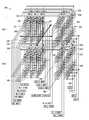
- FIG. 1shows a block diagram of an apparatus in the form of a memory device 100 , having a memory array 102 with memory cells 103 , according to an embodiment of the invention.
- Memory cells 103can be arranged in rows and columns along with lines 104 and lines 106 .
- Lines 104can carry signals WL 0 through WLm and can form part of access (e.g., word) lines of memory device 100 .
- Lines 106can carry signals BL 0 through BLn and can form part of data lines (e.g., bit lines) of memory device 100 .
- Memory device 100may use lines 104 to access memory cells 103 and lines 106 to exchange information (e.g., via signals provided on the lines 106 ) with memory cells 103 .
- a row decoder 107 and a column decoder 108decode address signals A 0 through AX on lines 109 (e.g., address lines) to determine which memory cells 103 are to be accessed in a memory operation.
- Memory device 100can perform memory operations, such as a read operation to read information from memory cells 103 , and a write (e.g., programming) operation to write (e.g., program) information into memory cells 103 .
- Memory device 100can also perform an erase operation to clear information from some or all of memory cells 103 .
- a memory control unit 118controls memory operations of the memory device 100 based on control signals on lines 120 .
- Examples of the control signals on lines 120include one or more clock signals and other signals to indicate which operation (e.g., read, programming, or erase operation) memory device 100 is to perform.
- Other devices external to memory device 100can control the values of the control signals on lines 120 .
- a memory access devicesuch as a processor or a memory controller
- Specific values of a combination of the signals on lines 120can produce a command (e.g., read, programming, or erase command) that can cause memory device 100 to perform a corresponding memory operation (e.g., read, programming, or erase operation).
- Memory device 100can include a selector 140 such as one or more select gates, configured to selectably couple memory cells 103 associated with lines 106 to sense circuits, such as data detectors 115 , in a memory operation, such as a read operation. Selector 140 and memory cells 103 can be physically located in the same memory array 102 . A portion of the memory array 102 can include memory cells 103 to store information. Another portion of memory array 102 can include the selector 140 .
- selector 140such as one or more select gates, configured to selectably couple memory cells 103 associated with lines 106 to sense circuits, such as data detectors 115 , in a memory operation, such as a read operation.
- Selector 140 and memory cells 103can be physically located in the same memory array 102 .
- a portion of the memory array 102can include memory cells 103 to store information. Another portion of memory array 102 can include the selector 140 .
- Data detectors 115are configured to determine the value of information from memory cells 103 in a memory operation, such as a read operation, and provides the information in the form of signals to lines 113 (e.g., data lines). Data detectors 115 can also use the signals on lines 113 to determine the value of information to be written (e.g., programmed) into memory cells 103 .
- Memory device 100can include an input/output (I/O) circuit 117 to exchange information between memory array 102 and lines (e.g., I/O lines) 105 .
- Signals DQ 0 through DQN on lines 105can represent information read from or to be written into memory cells 103 .
- Lines 105can include nodes within memory device 100 or pins (or solder balls, etc.) on a package where memory device 100 can reside.
- Other devices external to memory device 100e.g., a memory controller or a processor
- I/O circuit 117can respond to signals cSEL 1 through cSELn to select the signals on lines 113 that can represent the information read from or programmed into memory cells 103 .
- Column decoder 108can selectably activate the CSEL 1 through CSELn signals based on the A 0 through AX address signals on lines 109 .
- I/O circuit 117can select the signals on lines 113 to exchange information between memory array 102 and lines 105 during read and programming operations.
- Each of memory cells 103can be programmed to store information representing a value of a fraction of a bit, a value of a single bit or a value of multiple bits such as two, three, four, or another number of bits.
- each of memory cells 103can be programmed to store information representing a binary value “0” or “1” of a single bit.
- the single bit per cellis sometimes called a single level cell.
- each of memory cells 103can be programmed to store information representing a value representing multiple bits, such as one of four possible values “00”, “01”, “10”, and “11” of two bits, one of eight possible values “000”, “001”, “010”, “011”, “100”, “101”, “110”, and “111” of three bits, or one of other values of another number of multiple bits.
- a cell that has the ability to store multiple bitsis sometimes called a multi-level cell (or multi-state cell).
- Memory device 100can be configured to receive a supply voltage, including supply voltages Vcc and Vss, on lines 130 and 132 , respectively.
- Supply voltage Vsscan operate at a ground potential (e.g., having a value of approximately zero volts).
- Supply voltage Vcccan include an external voltage supplied to memory device 100 from an external power source such as a battery or an alternating-current to direct-current (AC-DC) converter circuitry.
- Memory device 100can include a non-volatile memory device and memory cells 103 can include non-volatile memory cells, such that memory cells 103 can retain information stored thereon when power (e.g., Vcc, Vss, or both) is disconnected from memory device 100 .
- memory device 100may comprise a flash memory device, such as a NAND flash or a NOR flash memory device, and/or another kind of memory device, such as a variable resistance memory device (e.g., a phase change or resistive RAM device).
- Memory device 100can include a memory device where memory cells 103 can be physically located in multiple levels on the same device, such that some of memory cells 103 can be stacked over some other memory cells 103 in multiple levels over a substrate (e.g., a semiconductor substrate) of memory device 100 .
- a substratee.g., a semiconductor substrate
- memory device 100may include other elements, several of which are not shown in FIG. 1 , so as not to obscure the embodiments described herein.
- Memory device 100may include memory devices and operate using memory operations (e.g., read, programming, and erase operations) similar to or identical to the memory devices and operations described below with reference to FIG. 2 through FIG. 18 .
- memory operationse.g., read, programming, and erase operations
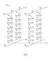
- FIG. 2shows a schematic diagram of a portion of a memory device 200 including memory cell strings 201 , 202 , 203 , and 204 , according to an embodiment of the invention.
- Memory device 200can be associated with memory device 100 of FIG. 1 , such as forming a portion of the memory array 102 of memory device 100 .
- memory cell strings 201 and 202can be coupled to line 270 at nodes 221 and 222 , respectively.
- Memory cell strings 203 and 204can be coupled to line 271 at nodes 223 and 224 , respectively.
- Each of the memory cell strings 201 , 202 , 203 , and 204can also be coupled to line 299 , which can be coupled to a line associated with a source (SRC).
- SRCsource
- Lines 270 and 271can be structured as conductive lines and can form part of the data lines (e.g., bit lines) of memory device 200 to carry signals BL 0 and BL 1 , respectively.
- Line 299can be structured as a conductive line and can form a part of a source line of the memory device 200 that carries signal SRC.
- memory cell string 201can include memory cells 210 with associated gates 231 , 232 , 233 , and 234 , and transistors 212 and 214 with associated gates 213 and 215 .
- Memory cell string 202can include memory cells 210 with associated gates 231 , 232 , 233 , and 234 , and transistors 216 and 218 with associated gates 217 and 219 .
- Memory cell string 203can include memory cells 211 with associated gates 231 , 232 , 233 , and 234 , and transistors 212 and 214 with associated gates 213 and 215 .
- Memory cell string 204can include memory cells 211 with associated gates 231 , 232 , 233 , and 234 , and transistors 216 and 218 with associated gates 217 and 219 .
- the memory cells ( 210 or 211 ) in each of memory cell strings 201 , 202 , 203 , and 204can be stacked over each other in multiple levels of the memory device 200 over a substrate (e.g., a semiconductor substrate) of the memory device 200 .
- Gates 213 of memory cell strings 201 and 203can be coupled together to carry the same signal SGDi.
- Gates 217 of memory cell strings 202 and 204can be coupled together to carry the same signal SGDj.
- Signals SGDi and SGDjcan be two different signals.
- Gates 215 of memory cell strings 201 and 203can be coupled together to carry the same signal SGSi.
- Gates 219 of memory cell strings 202 and 204can be coupled together to carry the same signal SGSj.
- Signals SGSi and SGSjcan be two different signals.
- Gates 231 of memory cell strings 201 , 202 , 203 , and 204can be coupled together to carry the same signal WL 0 .
- Gates 232 of memory cell strings 201 , 202 , 203 , and 204can be coupled together to carry the same signal WL 1 .
- Gates 233 of memory cell strings 201 , 202 , 203 , and 204can be coupled together to carry the same signal WL 2 .
- Gates 234 of memory cell strings 201 , 202 , 203 , and 204can be coupled together to carry the same signal WL 3 .
- FIG. 2shows an example of two lines (e.g., 270 and 271 ) and two memory cell strings coupled to each line with each string having four memory cells.
- the number of lines, memory cell strings, and memory cells in each memory cell stringsmay vary.
- a memory cell stringmay be configured with eight memory cells in each string, as shown in examples below.
- FIG. 3shows an apparatus 300 including a plurality of stacked arrays. For illustration purposes, two arrays are shown, including a first array 310 and a second array 330 . Although two arrays are shown, other example configurations include three or more arrays in the plurality of stacked arrays. Stacking arrays such as arrays 310 , 330 increases the density of memory per unit area on a semiconductor chip.
- the first array 310includes a number of memory cell strings 311 , arranged in rows along axis 313 and columns along axis 315 .
- the memory cell strings 311include NAND memory cell strings.
- the example of FIG. 3shows the memory cell strings 311 as substantially vertical memory cell strings oriented along vertical axis 317 .
- substantially straight, substantially vertical memory cell strings 311are used as an example, embodiments of the invention is not so limited.
- Other memory cell string configurationssuch as lateral, or U-shaped memory cell strings 311 may be used in accordance with some embodiments of the present invention.
- the memory cell strings 311are coupled between a source 312 and a data line 314 .
- a memory cell region 320is located in the middle of the memory cell strings 311 .
- a source select gate 316is shown located between the memory cell region 320 and the source 312 .
- a drain select gate 318is located between the memory cell region 320 and the data line 314 .
- the first arrayis shown with a first source 312 , and a first data line 314
- the second array 330is shown with a second source 332 and a second data line 334 .
- a data detector 340is also shown in FIG. 3 .
- the data detector 340is a shared data detector.
- the data detector 340is coupled to the second data line at node 342 , and is further coupled to the first data line 314 at node 344 .
- the data detectoris formed beneath the plurality of arrays in the apparatus 300 . Forming the data detector beneath the plurality of arrays can further improve device density by reducing a number of circuits that are formed on a periphery of arrays 310 , 330 .
- Examples of stacked array apparatuses using shared circuitry such as shared data detectorcan enable increased scaling of stacked arrays 310 , 330 , etc.
- larger circuits, such as data detectorscan be formed in reduced numbers while larger numbers of arrays are stacked.
- FIG. 4shows a block diagram of portions of the apparatus 300 from FIG. 3 .
- the source select gate 316is again shown located between the memory cell region 320 and the source 312 .
- the individual sources 312are shown coupled together as a source line.
- the drain select gate 318is again shown located between the memory cell region and the data line 314 .
- a number of individual memory cells 350are shown along the vertical axis of the memory cell string 311 .
- a number of access lines 352(e.g. wordlines) are shown to operate each of the individual memory cells 350 in the memory cell string 311 .
- a shared driveris used to drive corresponding access lines in each of the arrays.
- FIG. 5shows another example apparatus 500 including a plurality of stacked arrays.
- two arraysare shown, including a first array 510 and a second array 530 .
- other example configurationsinclude three or more arrays in the plurality of stacked arrays.
- the number of arrays in the plurality of stacked arraysis an even number of arrays as discussed below.
- the first array 510includes a number of memory cell strings 511 , arranged in rows along axis 513 and columns along axis 515 .
- the memory cell strings 511include NAND memory cell strings.
- FIG. 5shows the memory cell strings 511 as substantially vertical memory cell strings oriented along vertical axis 317 , although other configurations such as lateral strings or U-shaped strings may also be used.
- the memory cell strings 511are coupled between a source 512 and a data line 314 .
- a memory cell region 520is located in the middle of the memory cell strings 511 .
- a source select gate 518is shown located between the memory cell region 520 and the source 512 .
- a drain select gate 516is located between the memory cell region 520 and the data line 514 .
- the data line 514is a shared data line 514 .
- FIG. 5illustrates memory cell strings 534 in the second array 530 coupled between a source 532 and the shared data line 514 .
- a data detector 540is also shown in FIG. 5 .
- the data detector 540is a shared data detector (e.g., in this case, shared between the arrays 510 and 530 ).
- the data detector 540is coupled to the shared data line 514 at node 542 .
- two arrays 510 , 530are shown in the apparatus 500 .
- additional arraysare included and further stacked vertically along axis 517 .
- additional arraysare included in pairs, with each pair of arrays sharing one or more data lines similar to the first array 510 and the second array 530 .
- the number of arrays in the plurality of stacked arraysis an even number.
- an arrayis inverted with respect to a paired array to facilitate sharing of a data line.
- the first array 510is inverted with respect to the second array 530 .
- the source 512 of the first array 510is on the top of the first array 510
- the source 532 of the second array 530is on the bottom of the second array 530 .
- currentmay conduct from the respective sources 512 , 532 to the shared data line 514 , and be detected at the data detector 540 .
- FIG. 6shows a block diagram of portions of the apparatus 500 from FIG. 5 .
- the source select gate 516is again shown located between the memory cell region 520 and the source 512 .
- the drain select gate 518is again shown located between the memory cell region 520 and the data line 514 .
- a number of individual memory cells 550are shown along the vertical axis 517 of the memory cell string 511 .
- a number of access lines 552(e.g. wordlines) are shown to operate each of the individual memory cells 550 in the memory cell string 511 .
- a shared driveris used to drive corresponding access lines in each of the arrays.
- FIG. 7shows an apparatus 700 including a plurality of stacked arrays, including a first array 710 and a second array 730 . Although two arrays are shown, other example configurations include three or more arrays in the plurality of stacked arrays.
- the first array 710includes a number of memory cell strings 711 , arranged in rows along axis 713 and columns along axis 715 .
- the memory cell strings 711include NAND memory cell strings.
- the example of FIG. 7shows the memory cell strings 711 as substantially vertical memory cell strings oriented along vertical axis 717 . Although substantially straight, substantially vertical memory cell strings 711 are used as an example, other configurations such as lateral, or U-shapes memory cell strings 711 may be used in accordance with embodiments of the present invention.
- the memory cell strings 711 of the first array 710are coupled between a source 712 and a first data line 714 .
- a memory cell region 720is located in a middle of the memory cell strings 711 .
- a source select gate 716is shown located between the memory cell region 720 and the source 712 .
- FIG. 7includes a plurality of hierarchical select gates 721 coupled between the memory regions 720 and the data lines 714 .
- the plurality of hierarchical select gatesinclude a first select gate 718 and a second select gate 719 .
- a hierarchical select gate configurationoperates using a first select gate to select a number (referred to hereinafter as a “block”) of memory cell strings across more than one array in the plurality of stacked arrays.
- the hierarchical select gate configurationthen operates using a second select gate to select a number of memory cell strings from within the block selected by the first select gate (e.g., the strings of the selected block within a selected one of stacked arrays 710 and 730 ).
- Configurations using a hierarchical select gate configurationcan reduce an amount of memory cell string selection circuitry (for example selection circuitry 140 from FIG. 1 ) and further increase device density on a given semiconductor surface.
- the first array 710is shown with a first source 712 , and a first data line 714
- the second array 720is shown with a second source 732 and a second data line 734
- a data detector 740is also shown in FIG. 7 .
- the data detector 740is a shared data detector.
- the data detector 740is coupled to the second data line 734 at node 742 , and is further coupled to the first data line 714 at node 744 .
- the data detectoris formed beneath the plurality of arrays in the apparatus 700 .
- FIG. 8shows a block diagram of portions of the apparatus 700 from FIG. 7 .
- the source select gate 716is again shown located between the memory cell region 720 and the source 712 .
- the hierarchical select gates 721are shown coupled between the memory regions 720 and the data lines 714 .
- the hierarchical select gates 721show the first select gate 718 to select a row of blocks.
- the hierarchical select gates 721further show the second select gate 719 to select an array level within a selected one of stacked arrays 710 and 730 that are within the selected block 760 of memory cell strings.
- a number of individual memory cells 750are shown along the vertical axis 717 of the memory cell string 711 .
- a number of access lines 752(e.g. wordlines) are shown to operate each of the individual memory cells 750 in the memory cell string 711 .
- FIG. 9shows another example apparatus 900 including a plurality of stacked arrays.
- two arraysare shown, including a first array 910 and a second array 930 .
- other example configurationsinclude three or more arrays in the plurality of stacked arrays.
- the number of arrays in the plurality of stacked arraysis an even number of arrays as discussed below.
- the first array 910includes a number of memory cell strings 911 , arranged in rows along axis 913 and columns along axis 915 .
- the memory cell strings 911include NAND memory cell strings.
- FIG. 9shows the memory cell strings 911 as vertical memory cell strings oriented along vertical axis 917 , although other configurations such as lateral strings or U-shaped strings may also be used.
- the memory cell strings 911are coupled between a source 912 and a data line 914 .
- a memory cell region 920is located in a middle of the memory cell strings 911 .
- a source select gate 916is shown located between the memory cell region 920 and the source 912 .
- the data line 914is a shared data line 914 .
- FIG. 9illustrates memory cell strings 934 in the second array 930 coupled between a source 932 and the shared data line 914 .
- FIG. 9further includes a plurality of hierarchical select gates 921 coupled between the memory cell regions 920 and the shared data line 914 .
- the plurality of hierarchical select gatesinclude a first select gate 918 and a second select gate 919 .
- a hierarchical select gate configurationoperates using a first select gate to select a row of blocks 960 of memory cell strings across more than one array in the plurality of stacked arrays. The hierarchical select gate configuration then operates using a second select gate to select an array level of cell strings from within the selected row of blocks of memory cell strings selected by the first select gate.
- a data detector 940is also shown in FIG. 9 .
- the data detector 940is a shared data detector.
- the data detector 940is coupled to the shared data line 914 at node 942 .
- two arrays 910 , 930are shown in the apparatus 900 .
- additional arraysare included and further stacked vertically along axis 917 .
- additional arraysare included in pairs, with each pair of arrays sharing one or more data lines similar to the first array 910 and the second array 930 .
- the number of arrays in the plurality of stacked arraysis an even number.
- an arrayis inverted with respect to a paired array to facilitate sharing of a data line.
- the first array 910is inverted with respect to the second array 930 .
- the source 912 of the first array 910is on the top of the first array 910
- the source 932 of the second array 930is on the bottom of the second array 930 .
- currentmay conduct from the respective sources 912 , 932 to the shared data line 914 , and be detected at the data detector 940 .
- FIG. 10shows a block diagram of portions of the apparatus 900 from FIG. 9 .
- the source select gate 916is again shown located between the memory cell region 920 and the source 912 .
- the hierarchical select gates 921are shown coupled between the memory cell regions 920 and the shared data line 914 .
- the hierarchical select gates 921show the first select gate 918 to select a row of blocks 960 of memory cell strings.
- the hierarchical select gates 921further show the second select gate 919 to select an array level of cell strings within a selected one of stacked arrays 910 and 930 that are within the selected row of blocks 960 .
- a number of individual memory cells 950are shown along the vertical axis 917 of the memory cell string 911 .
- a number of access lines 952are shown to operate each of the individual memory cells 950 in the memory cell string 911 .
- FIG. 11shows an apparatus 1100 including a plurality of stacked arrays, including a first array 1110 and a second array 1130 . Although two arrays are shown, other example configurations include three or more arrays in the plurality of stacked arrays.
- the first array 1110includes a number of memory cell strings 1111 , arranged in rows along axis 1113 and columns along axis 1115 .
- the memory cell strings 1111include NAND memory cell strings.
- FIG. 11shows the memory cell strings 1111 as substantially vertical memory cell strings oriented along vertical axis 1117 .
- substantially straight, substantially vertical memory cell strings 1111are used as an example, other configurations such as lateral, or U-shapes memory cell strings 1111 may be used in accordance with embodiments of the present invention.
- the memory cell strings 1111 of the first array 1110are coupled between a source 1112 and a first data plate 1114 .
- the first data plate 1114is coupled to multiple memory cell strings 1111 in both the row axis 1113 and the column axis 1115 as shown in the Figure.
- the first data plate 1114is coupled to four columns in the row axis 1113 , and complete rows in the column axis 1115 , as shown in similar examples above.
- a memory cell region 1120is located in a middle of the memory cell strings 1111 .
- a source select gate 1116is shown located between the memory cell region 1120 and the source 1112 .
- FIG. 11includes a plurality of select gates 1121 coupled between the memory cell regions 1120 and the data plate 1114 .
- the plurality of select gatesinclude a first select gate 1118 and a second select gate 1119 .
- the select gate configurationoperates using a first select gate to select a row of blocks 1160 .
- the select gate configurationthen operates using a second select gate to select a column of blocks 1160 from within the blocks of memory cell strings selected by the first select gate.
- Configurations using such a select gate configurationcan reduce an amount of memory cell string selection circuitry, and further increase device density on a given semiconductor surface.
- the first array 1110is shown with a first source 1112 , and a first data plate 1114
- the second array 1130is shown with a second source 1132 and a second data plate 1134
- a data detector 1140is also shown in FIG. 11 .
- the data detector DDC0 1140is coupled to the second data plate 1134 at node 1142 .
- the data detectorsare formed beneath the plurality of arrays in the apparatus 1100 .
- data plates 1114 , 1134more memory cell strings 1111 are coupled to a single data detector 1140 , and chip area may be further saved.
- FIG. 12shows a block diagram of portions of the apparatus 1100 from FIG. 11 .
- the source select gate 1116is again shown located between the memory cell region 1120 and the source 1112 .
- the select gates 1121are shown coupled between the memory cell regions 1120 and the data plate 1114 .
- the select gates 1121show the first select gate 1118 to select a row of blocks 1160 .
- the select gates 1121further show the second select gate 1119 to select a column of blocks 1160 .
- a number of individual memory cells 1150are shown along the vertical axis 1117 of the memory cell string 1111 .
- a number of access lines 1152are shown to operate each of the individual memory cells 1150 in the memory cell string 1111 .
- FIG. 13shows a block diagram of portions of an apparatus 1300 including a plurality of stacked arrays, including a first array 1310 and a second array 1330 .
- a source select gate 1316is shown located between a memory cell region 1320 and a source 1312 .
- Select gates 1321are shown coupled between the memory cell regions in the first array 1310 , and a data plate 1314 .
- the data plate 1314is a shared data plate.
- Select gates 1331are further shown coupled between the memory cell regions 1320 in the second array 1330 , and the shared data plate 1314 .
- the shared data plate 1314is shared between two columns in the first array 1310 and two columns in the second array 1330 for a total of four columns. Other configurations of shared data plates may couple to other numbers of columns in the first and second arrays 1310 , 1330 .
- the select gates 1321show a first select gate 1318 in the first array 1310 and a first select gate 1338 in the second array 1330 coupled together and used to select a row of blocks 1360 .
- the select gates 1121further show second select gates 1319 in the first array 1310 and second select gates 1339 in the second array 1330 to select a column of blocks 1360 .
- two arrays 1310 , 1330are shown in the apparatus 1300 .
- additional arraysare included and further stacked vertically along axis 1317 .
- additional arraysare included in pairs, with each pair of arrays sharing one or more data plates 1314 similar to the first array 1310 and the second array 1330 .
- the number of arrays in the plurality of stacked arraysis an even number.
- an arrayis inverted with respect to a paired array to facilitate sharing of a data plate.
- the first array 1310is inverted with respect to the second array 1330 .
- the source 1312 of the first array 1310is on the top of the first array 1310
- a source 1332 of the second array 1330is on the bottom of the second array 1330 .
- currentis conducted from the respective sources 1312 , 1332 to the shared data plate 1314 , and be detected at an attached data detector (not shown).
- FIG. 14shows an apparatus 1400 including a plurality of stacked arrays. For illustration purposes, two arrays are shown, including a first array 1410 and a second array 1430 . Although two arrays are shown, other example configurations include three or more arrays in the plurality of stacked arrays. Stacking arrays such as arrays 1410 , 1430 increases a density of memory per unit area on a semiconductor chip.
- the first array 1410includes a number of memory cell strings 1411 , arranged in rows along axis 1413 and columns along axis 1415 .
- the memory cell strings 1411include NAND memory cell strings.
- the example of FIG. 14shows the memory cell strings 1411 as substantially vertical memory cell strings oriented along vertical axis 1417 . Although substantially straight, substantially vertical memory cell strings 1411 are used as an example, other memory cell string configurations such as lateral, or U-shapes memory cell strings 1411 may be used in accordance with embodiments of the present invention.
- the memory cell strings 1411are coupled between a source 1412 and a data line 1414 .
- a memory cell region 1420is located in a middle of the memory cell strings 1411 .
- a source select gate 1416is shown located between the memory cell region 1420 and the source 1412 .
- a drain select gate 1418is located between the memory cell region 1420 and the data line 1414 .
- the first arrayis shown with a first source 1412
- the second array 1430is shown with a second source 1432 and a second data line 1434 .
- a data detector 1440is also shown in FIG. 14 .
- the data detector 1440is a shared data detector.
- the data detector 1440is selectably coupled to the second data line 1434 at node 1442 through a switch such as example switch 1446 , and is further selectably coupled to the first data line 1414 at node 1444 through a switch such as example switch 1466 .
- a shared data detector 1440chip area can be saved, and device density can be improved.
- an inhibit voltage source 1450is also shown in FIG. 14 .
- the inhibit voltage source 1450is a shared inhibit voltage source 1450 .
- the inhibit voltage source 1450is selectably coupled to the second data line 1434 at node 1452 through switch 1456 , and is further selectably coupled to the first data line 1414 at node 1454 through a switch such as example switch 1468 .
- a shared inhibit voltage source 1450chip area can be saved, and device density can be improved.
- By selective coupling the data detector 1440 and the inhibit voltage source 1450a string in one array within the plurality of stacked arrays can be inhibited while a string in another array within the plurality of stacked arrays is utilizing the data detector 1440 .
- Examples including an inhibit voltage source 1450may use the inhibit voltage source 1450 to reduce unwanted disturbing of a data state in memory cells within memory cell strings. For example a reverse bias within the memory cell region 1420 inhibits unwanted charge migration from floating gates within the memory cell region 1420 .
- the data detector 1440is selectably coupled to the data line 1434 through switch 1446 .
- the use of switches 1446provides efficiency in manufacturing because similar structures are already being manufactured within the arrays 1410 , 1430 to form memory cell strings.
- Switch 1446includes at least one select gate 1447 , similar to other select gates 1418 already being formed within the arrays 1410 , 1430 .
- the select gate 1447provides selective coupling of the data detector 1440 to the data line 1434 .
- the inhibit voltage source 1450is coupled to the data line 1434 through switch 1456 .
- the use of switches 1456provides efficiency in manufacturing because similar structures are already being manufactured within the arrays 1410 , 1430 to form memory cell strings.
- Switch 1456includes at least one select gate 1457 that provides selective coupling of the inhibit voltage source 1450 to the data line 1434 .
- FIG. 15shows a block diagram of portions of the apparatus 1400 from FIG. 14 .
- the source select gate 1416is again shown located between the memory cell region and the source 1412 .
- the drain select gate 1418is again shown located between the memory cell region and the data line 1414 .
- a number of individual memory cells 1470are shown along the vertical axis of the memory cell string 1411 .
- a number of access lines 1472(e.g. wordlines) are shown to operate each of the individual memory cells 1470 in the memory cell string 1411 .
- the inhibit voltage source 1450 and the data detector 1440are further shown in FIG. 15 , selectably coupled to the data line 1434 by respective switches 1456 , 1446 .
- select gates 1457 and 1447By appropriate selection, using select gates 1457 and 1447 , memory cell strings within a selected block within the plurality of stacked arrays can be either inhibited from electrical disturbance, or coupled to data detector 1440 to have their data state read.
- FIG. 16shows an apparatus 1600 including a plurality of stacked arrays. For illustration purposes, two arrays are shown, including a first array 1610 and a second array 1630 . Although two arrays are shown, other example configurations include three or more arrays in the plurality of stacked arrays. Stacking arrays such as arrays 1610 , 1630 increases a density of memory per unit area on a semiconductor chip.
- the first array 1610includes a number of memory cell strings 1611 , arranged in rows along axis 1613 and columns along axis 1615 .
- the memory cell strings 1611include NAND memory cell strings.
- the example of FIG. 16shows the memory cell strings 1611 as substantially vertical memory cell strings oriented along vertical axis 1617 . Although substantially straight, substantially vertical memory cell strings 1611 are used as an example, other memory cell string configurations such as lateral, or U-shapes memory cell strings 1611 may be used in accordance with embodiments of the present invention.
- the memory cell strings 1611are coupled between a source 1612 and a data line 1614 .
- a memory cell region 1620is located in a middle of the memory cell strings 1611 .
- a source select gate 1616is shown located between the memory cell region 1620 and the source 1612 .
- a drain select gate 1618is located between the memory cell region 1620 and the data line 1614 .
- a data detector 1640is also shown in FIG. 16 .
- the data detector 1640is a shared data detector (in this case shared between a number of data lines of the same array as opposed to data lines of different arrays).
- the data detector 1640is selectably coupled to a first data line 1634 through detector plate 1642 and switches such as switch 1646 , and is further selectably coupled to second, third and fourth data lines (not currently labeled) through detector plate 1642 and switches such as switch 1646 .
- a shared data detector 1640chip area can be saved, and device density can be improved.
- each detector plate 1642 , 1644is selectably coupled to four adjacent data lines by switches. Four adjacent data lines are used as an example. Other numbers of data lines may be selectably coupled to a detector plate in other examples.
- an inhibit voltage source 1650is also shown in FIG. 16 .
- the inhibit voltage source 1650is a shared inhibit voltage source 1650 .
- the inhibit voltage source 1650is selectably coupled to the first data line 1634 through inhibit source plate 1652 and switch 1656 .
- the inhibit voltage source 1650is also selectably coupled to the second, third, fourth, sixth, seventh and eighth data lines (not currently labeled). Similar to the detector plate described above, by using an inhibit source plate 1652 , chip area may be further saved by selectably coupling the inhibit voltage source 1650 to more than one data line of the same array 1630 (and possibly to data lines, such as data line 1614 , of other arrays).
- a shared inhibit voltage source 1650By using a shared inhibit voltage source 1650 , chip area can be saved, and device density can be improved. By using selective coupling of the data detector 1640 and the inhibit voltage source 1650 , a selected memory cell string, or groups of memory cell strings within the plurality of stacked arrays can be inhibited while another memory cell string within the plurality of stacked arrays utilize the data detector 1640 .
- the data plate 1642 and the inhibit source plate 1652may selectably couple to different numbers of data lines of the same array 1630 .
- a single inhibit source plate 1652is shown coupled to a number of data lines of the second array 1630 , while multiple data plates (including data plate 1642 ) are coupled to the same number of data lines of the second array 1630 .
- An inhibit voltage source 1650may be able to effectively drive a voltage to a large number of data lines, while a given data detector 1640 may be limited in a number of data lines that it can effectively service. In such a configuration, it may be desirable to have a single inhibit source plate 1652 selectably coupled to a number of data lines, while multiple data plates 1642 are selectably coupled to the same data lines.
- the data detector 1640is selectably coupled to the data lines (e.g., data line 1634 ) through a switch (e.g., switch 1646 ).
- switch 1646also includes at least one select gate 1647 , similar to other select gates 1618 already being formed within the arrays 1610 , 1630 .
- the inhibit voltage source 1650is selectably coupled to the data lines (e.g., data line 1634 ) through switches, such as switch 1656 .
- FIG. 17shows a block diagram of portions of the apparatus 1600 from FIG. 16 .
- the source select gate 1616is again shown located between the memory cell region 1620 and the source 1612 .
- the drain select gate 1618is again shown located between the memory cell region 1620 and the data line 1614 .
- a number of individual memory cells 1670are shown along the vertical axis of the memory cell string 1611 .
- a number of access lines 1672(e.g. wordlines) are shown to operate each of the individual memory cells 1670 in the memory cell string 1611 .
- the inhibit voltage source 1650 and the data detector 1640are further shown in FIG. 17 , selectably coupled to the data line 1634 by respective switches 1656 , 1646 .
- select gates 1657 and 1647By appropriate selection, using select gates 1657 and 1647 , a memory cell string coupled to the data line 1634 can be either inhibited from electrical disturbance, or coupled to data detector 1640 to have a data state read.
- FIG. 18shows an example method of operation that may be used with selected apparatus examples described.
- a first memory cell stringis selected in a first array within a plurality of stacked arrays.
- the data state of a memory cell within the first memory cell stringis detected at a shared data detector.
- a second memory cell stringis selected in a second array within a plurality of stacked arrays.
- the data state of a memory cell within the second memory cell stringis detected at the shared data detector.
- FIG. 19shows another example method of operation that may be used with selected apparatus examples described.
- a plurality of memory cell stringsare selected across more than one array within a plurality of stacked arrays using a first select gate.
- a memory cell string of the selected plurality of memory cell stringsis selected using a second select gate.
- the data state of a memory cell within the selected memory cell stringis detected.
- FIG. 20shows another example method of operation that may be used with selected apparatus examples described.
- a first memory cell stringis selected in an array of a plurality of stacked arrays.
- the data state of a memory cell within the first memory cell stringis detected at a shared data detector.
- electrical disturbanceis inhibited in a second memory cell string in the plurality of stacked arrays using a shared inhibit voltage source.
- FIG. 21is a block diagram of an information handling system 2100 incorporating at least one chip or chip assembly 2104 that includes a memory device 307 according to an embodiment of the invention.
- the memory device 307includes a plurality of stacked arrays of memory cell strings as described in any of the embodiments previously described.
- the information handling system 2100 shown in FIG. 21is merely one example of a system in which the present invention can be used.
- Other examplesinclude, but are not limited to, personal data assistants (PDAs), video game consoles, telephones, MP3 players, aircraft, satellites, military vehicles, etc.
- information handling system 2100comprises a data processing system that includes a system bus 2102 to couple the various components of the system.
- System bus 2102provides communications links among the various components of the information handling system 2100 and may be implemented as a single bus, as a combination of busses, or in any other suitable manner.
- Chip assembly 2104is coupled to the system bus 2102 .
- Chip assembly 204may include any circuit or operably compatible combination of circuits.
- chip assembly 2104includes a processor 2106 that can be of any type.
- processormeans any type of computational circuit such as, but not limited to, a microprocessor, a microcontroller, a graphics processor, a digital signal processor (DSP), or any other type of processor or processing circuit. Multiple processors such as “multi-core” devices are also within the scope of the invention.
- a memory device 2107including any memory device or array of devices described previously, is included in the chip assembly 2104 .
- Those of ordinary skill in the artwill recognize that a wide variety of memory device configurations may be used in the chip assembly 2104 . Acceptable types of memory chips include, but are not limited to, non-volatile memory configurations such as NAND memory or NOR memory.
- additional logic chips 2108 other than processor chipsare included in the chip assembly 2104 .
- An example of a logic chip 2108 other than a processorincludes an analog to digital converter.
- Other circuits on logic chips 2108such as custom circuits, an application-specific integrated circuit (ASIC), etc. are also included in one embodiment of the invention.
- Information handling system 2100may also include an external memory 2111 , which in turn can include one or more memory elements suitable to the particular application, such as one or more hard drives 2112 , and/or one or more drives that handle removable media 2113 such as compact disks (CDs), digital video disks (DVDs), flash drives and the like.
- an external memory 2111can include one or more memory elements suitable to the particular application, such as one or more hard drives 2112 , and/or one or more drives that handle removable media 2113 such as compact disks (CDs), digital video disks (DVDs), flash drives and the like.
- CDscompact disks
- DVDsdigital video disks
- flash drivesand the like.
- a memory constructed as described in any of the previous examplescan be included in the external memory 2111 of the information handling system 2100 .
- Information handling system 2100may also include a display device 309 such as a monitor, additional peripheral components 2110 , such as speakers, etc. and a keyboard and/or controller 2114 , which can include a mouse, touch screen, or any other device that permits a system user to input information into and receive information from the information handling system 2100 .
- a display device 309such as a monitor
- additional peripheral components 2110such as speakers, etc.
- a keyboard and/or controller 2114which can include a mouse, touch screen, or any other device that permits a system user to input information into and receive information from the information handling system 2100 .
Landscapes
- Engineering & Computer Science (AREA)
- Microelectronics & Electronic Packaging (AREA)
- Semiconductor Memories (AREA)
- Non-Volatile Memory (AREA)
- Read Only Memory (AREA)
Abstract
Description
Claims (49)
Priority Applications (8)
| Application Number | Priority Date | Filing Date | Title |
|---|---|---|---|
| US13/524,872US8964474B2 (en) | 2012-06-15 | 2012-06-15 | Architecture for 3-D NAND memory |
| PCT/US2013/045173WO2013188399A1 (en) | 2012-06-15 | 2013-06-11 | Architecture for 3-d nand memory |
| TW102121223ATWI524356B (en) | 2012-06-15 | 2013-06-14 | Architecture for 3-d nand memory |
| TW107136222ATWI680464B (en) | 2012-06-15 | 2013-06-14 | Architecture for 3-d nand memory |
| TW104143893ATWI643202B (en) | 2012-06-15 | 2013-06-14 | Architecture for 3-d nand memory |
| US14/626,540US10269429B2 (en) | 2012-06-15 | 2015-02-19 | Architecture for 3-D NAND memory |
| US16/378,090US10803944B2 (en) | 2012-06-15 | 2019-04-08 | Architecture for 3-D NAND memory |
| US17/067,577US11380397B2 (en) | 2012-06-15 | 2020-10-09 | Architecture for 3-D NAND memory |
Applications Claiming Priority (1)
| Application Number | Priority Date | Filing Date | Title |
|---|---|---|---|
| US13/524,872US8964474B2 (en) | 2012-06-15 | 2012-06-15 | Architecture for 3-D NAND memory |
Related Child Applications (1)
| Application Number | Title | Priority Date | Filing Date |
|---|---|---|---|
| US14/626,540ContinuationUS10269429B2 (en) | 2012-06-15 | 2015-02-19 | Architecture for 3-D NAND memory |
Publications (2)
| Publication Number | Publication Date |
|---|---|
| US20130336065A1 US20130336065A1 (en) | 2013-12-19 |
| US8964474B2true US8964474B2 (en) | 2015-02-24 |
Family
ID=49755771
Family Applications (4)
| Application Number | Title | Priority Date | Filing Date |
|---|---|---|---|
| US13/524,872Active2032-08-06US8964474B2 (en) | 2012-06-15 | 2012-06-15 | Architecture for 3-D NAND memory |
| US14/626,540ActiveUS10269429B2 (en) | 2012-06-15 | 2015-02-19 | Architecture for 3-D NAND memory |
| US16/378,090ActiveUS10803944B2 (en) | 2012-06-15 | 2019-04-08 | Architecture for 3-D NAND memory |
| US17/067,577ActiveUS11380397B2 (en) | 2012-06-15 | 2020-10-09 | Architecture for 3-D NAND memory |
Family Applications After (3)
| Application Number | Title | Priority Date | Filing Date |
|---|---|---|---|
| US14/626,540ActiveUS10269429B2 (en) | 2012-06-15 | 2015-02-19 | Architecture for 3-D NAND memory |
| US16/378,090ActiveUS10803944B2 (en) | 2012-06-15 | 2019-04-08 | Architecture for 3-D NAND memory |
| US17/067,577ActiveUS11380397B2 (en) | 2012-06-15 | 2020-10-09 | Architecture for 3-D NAND memory |
Country Status (3)
| Country | Link |
|---|---|
| US (4) | US8964474B2 (en) |
| TW (3) | TWI524356B (en) |
| WO (1) | WO2013188399A1 (en) |
Cited By (8)
| Publication number | Priority date | Publication date | Assignee | Title |
|---|---|---|---|---|
| US20150162084A1 (en)* | 2012-06-15 | 2015-06-11 | Micron Technology, Inc. | Architecture for 3-d nand memory |
| US9679650B1 (en) | 2016-05-06 | 2017-06-13 | Micron Technology, Inc. | 3D NAND memory Z-decoder |
| US10170188B1 (en)* | 2017-08-31 | 2019-01-01 | Micron Technology, Inc. | 3D memory device including shared select gate connections between memory blocks |
| US10366738B2 (en)* | 2017-01-30 | 2019-07-30 | Micron Technology, Inc. | Integrated memory assemblies comprising multiple memory array decks |
| US20200027509A1 (en)* | 2018-07-20 | 2020-01-23 | Yangtze Memory Technologies Co., Ltd. | Three-dimensional memory devices |
| US10580790B2 (en) | 2011-04-28 | 2020-03-03 | Micron Technology, Inc. | Semiconductor apparatus with multiple tiers, and methods |
| US11450381B2 (en) | 2019-08-21 | 2022-09-20 | Micron Technology, Inc. | Multi-deck memory device including buffer circuitry under array |
| US20240260264A1 (en)* | 2023-01-27 | 2024-08-01 | SK Hynix Inc. | Semiconductor device having channel isolation structure |
Families Citing this family (16)
| Publication number | Priority date | Publication date | Assignee | Title |
|---|---|---|---|---|
| US9093152B2 (en) | 2012-10-26 | 2015-07-28 | Micron Technology, Inc. | Multiple data line memory and methods |
| US9147493B2 (en) | 2013-06-17 | 2015-09-29 | Micron Technology, Inc. | Shielded vertically stacked data line architecture for memory |
| US9324437B2 (en) | 2014-07-30 | 2016-04-26 | Macronix International Co., Ltd. | Systems and methods for trimming control transistors for 3D NAND flash |
| US10074430B2 (en)* | 2016-08-08 | 2018-09-11 | Micron Technology, Inc. | Multi-deck memory device with access line and data line segregation between decks and method of operation thereof |
| US10262715B2 (en) | 2017-03-27 | 2019-04-16 | Micron Technology, Inc. | Multiple plate line architecture for multideck memory array |
| CN109690776B (en) | 2018-12-07 | 2020-01-10 | 长江存储科技有限责任公司 | Novel 3D NAND memory device and method of forming the same |
| US10580795B1 (en) | 2019-08-15 | 2020-03-03 | Micron Technology, Inc. | Microelectronic devices including staircase structures, and related memory devices and electronic systems |
| US11508746B2 (en)* | 2019-10-25 | 2022-11-22 | Micron Technology, Inc. | Semiconductor device having a stack of data lines with conductive structures on both sides thereof |
| US11217601B2 (en) | 2019-10-29 | 2022-01-04 | Micron Technology, Inc. | Microelectronic devices including staircase structures, and related memory devices and electronic systems |
| US11309328B2 (en) | 2019-10-29 | 2022-04-19 | Micron Technology, Inc. | Methods of forming microelectronic devices, and related microelectronic devices, memory devices, and electronic systems |
| US11605588B2 (en) | 2019-12-20 | 2023-03-14 | Micron Technology, Inc. | Memory device including data lines on multiple device levels |
| US11424262B2 (en) | 2020-03-17 | 2022-08-23 | Micron Technology, Inc. | Microelectronic devices including staircase structures, and related memory devices and electronic systems |
| US11423960B2 (en)* | 2020-10-30 | 2022-08-23 | Taiwan Semiconductor Manufacturing Co., Ltd. | Memory device |
| JP2022191630A (en)* | 2021-06-16 | 2022-12-28 | キオクシア株式会社 | semiconductor storage device |
| US20240055045A1 (en)* | 2022-08-12 | 2024-02-15 | Ap Memory Technology Corporation | Memory device having segmented data line structure |
| US20240179908A1 (en)* | 2022-11-29 | 2024-05-30 | Sandisk Technologies Llc | Three-dimensional memory device including a mid-stack source layer and methods for forming the same |
Citations (16)
| Publication number | Priority date | Publication date | Assignee | Title |
|---|---|---|---|---|
| US3825907A (en) | 1971-07-26 | 1974-07-23 | Ampex | Planar core memory stack |
| US4811082A (en) | 1986-11-12 | 1989-03-07 | International Business Machines Corporation | High performance integrated circuit packaging structure |
| US5732018A (en)* | 1995-10-30 | 1998-03-24 | Samsung Electronics Co., Ltd. | Self-contained reprogramming nonvolatile integrated circuit memory devices and methods |
| US20050226049A1 (en) | 2004-04-09 | 2005-10-13 | Samsung Electronics Co., Ltd. | NOR flash memory device and method of shortening a program time |
| US20060146608A1 (en)* | 2004-12-30 | 2006-07-06 | Matrix Semiconductor, Inc. | Integrated circuit including memory array incorporating multiple types of NAND string structures |
| US20060203547A1 (en)* | 2005-03-09 | 2006-09-14 | Kabushiki Kaisha Toshiba | Semiconductor memory device |
| US20090168534A1 (en) | 2008-01-02 | 2009-07-02 | Samsung Electronics Co., Ltd. | Three-dimensional memory device with multi-plane architecture |
| US20090267139A1 (en)* | 2008-04-23 | 2009-10-29 | Hiroshi Maejima | Three dimensional stacked nonvolatile semiconductor memory |
| US20090268524A1 (en)* | 2008-04-23 | 2009-10-29 | Hiroshi Maejima | Three dimensional stacked nonvolatile semiconductor memory |
| US20100321998A1 (en)* | 2009-06-22 | 2010-12-23 | Samsung Electronics Co., Ltd. | Nonvolatile memory device and related method of programming |
| US20100322000A1 (en) | 2009-06-19 | 2010-12-23 | Samsung Electronics Co., Ltd. | Programming methods for three-dimensional memory devices having multi-bit programming, and three-dimensional memory devices programmed thereby |
| US7859902B2 (en) | 2008-04-23 | 2010-12-28 | Kabushiki Kaisha Toshiba | Three dimensional stacked nonvolatile semiconductor memory |
| US20110063916A1 (en) | 2009-09-14 | 2011-03-17 | Kabushiki Kaisha Toshiba | Non-volatile semiconductor storage device |
| US20110182105A1 (en) | 2008-08-25 | 2011-07-28 | Tianhong Yan | Memory system with sectional data lines |
| US20110286283A1 (en) | 2010-05-21 | 2011-11-24 | Macronix International Co., Ltd. | 3d two-bit-per-cell nand flash memory |
| WO2013188399A1 (en) | 2012-06-15 | 2013-12-19 | Micron Technology, Inc. | Architecture for 3-d nand memory |
Family Cites Families (127)
| Publication number | Priority date | Publication date | Assignee | Title |
|---|---|---|---|---|
| US5680347A (en) | 1994-06-29 | 1997-10-21 | Kabushiki Kaisha Toshiba | Nonvolatile semiconductor memory device |
| JP3544743B2 (en) | 1995-04-17 | 2004-07-21 | 株式会社東芝 | Semiconductor storage device |
| KR0172443B1 (en)* | 1995-09-19 | 1999-03-30 | 김광호 | Cell connection method and non-volatile circuit of nonvolatile semiconductor memory |
| KR100205240B1 (en)* | 1996-09-13 | 1999-07-01 | 윤종용 | Nonvolatile Semiconductor Memory Device with Single and Multiple Bit Cells |
| KR100200930B1 (en) | 1996-12-06 | 1999-06-15 | 윤종용 | Row Decoder for Semiconductor Memory Device Suitable for Burst Mode Operation |
| US6344814B1 (en) | 1999-12-10 | 2002-02-05 | Winbond Electronics Corporation | Driving circuit |
| JP3543946B2 (en) | 2000-04-14 | 2004-07-21 | 日本電気株式会社 | Field effect transistor and method of manufacturing the same |
| JP4157269B2 (en) | 2000-06-09 | 2008-10-01 | 株式会社東芝 | Semiconductor memory device |
| JP3770171B2 (en) | 2002-02-01 | 2006-04-26 | ソニー株式会社 | Memory device and memory system using the same |
| AU2003201760A1 (en) | 2002-04-04 | 2003-10-20 | Kabushiki Kaisha Toshiba | Phase-change memory device |
| US6903982B2 (en) | 2002-10-10 | 2005-06-07 | Infineon Technologies Ag | Bit line segmenting in random access memories |
| JP4713143B2 (en)* | 2004-12-15 | 2011-06-29 | 富士通セミコンダクター株式会社 | Semiconductor memory device |
| KR100702011B1 (en) | 2005-03-16 | 2007-03-30 | 삼성전자주식회사 | CMOS SRAM Cells Employing Multiple Gate Transistors and Methods of Manufacturing the Same |
| KR100666174B1 (en)* | 2005-04-27 | 2007-01-09 | 삼성전자주식회사 | 3-level nonvolatile semiconductor memory device and driving method thereof |
| JP4762986B2 (en) | 2005-06-30 | 2011-08-31 | スパンション エルエルシー | Nonvolatile memory device and control method of nonvolatile memory device |
| US20090224330A1 (en) | 2005-07-28 | 2009-09-10 | Hong Chang Min | Semiconductor Memory Device and Method for Arranging and Manufacturing the Same |
| KR20100003629A (en) | 2008-07-01 | 2010-01-11 | 삼성전자주식회사 | Semiconductor memory device comprising stacked transistors and method of manufacturing the same |
| US7212447B2 (en) | 2005-08-04 | 2007-05-01 | Micron Technology, Inc. | NAND flash memory cell programming |
| TWI266423B (en) | 2005-12-23 | 2006-11-11 | Ind Tech Res Inst | Three-dimensional thin-film transistor nano-die memory device and manufacturing method thereof |
| JP5016832B2 (en) | 2006-03-27 | 2012-09-05 | 株式会社東芝 | Nonvolatile semiconductor memory device and manufacturing method thereof |
| US7554832B2 (en) | 2006-07-31 | 2009-06-30 | Sandisk 3D Llc | Passive element memory array incorporating reversible polarity word line and bit line decoders |
| US7499366B2 (en) | 2006-07-31 | 2009-03-03 | Sandisk 3D Llc | Method for using dual data-dependent busses for coupling read/write circuits to a memory array |
| JP5100080B2 (en) | 2006-10-17 | 2012-12-19 | 株式会社東芝 | Nonvolatile semiconductor memory device and manufacturing method thereof |
| JP4945248B2 (en) | 2007-01-05 | 2012-06-06 | 株式会社東芝 | Memory system, semiconductor memory device and driving method thereof |
| US7800400B2 (en)* | 2007-01-12 | 2010-09-21 | Altera Corporation | Configuration random access memory |
| JP5460950B2 (en) | 2007-06-06 | 2014-04-02 | ピーエスフォー ルクスコ エスエイアールエル | Semiconductor device and manufacturing method thereof |
| CN101548336B (en) | 2007-06-22 | 2012-07-11 | 松下电器产业株式会社 | Resistance variable nonvolatile memory device |
| JP2009212280A (en) | 2008-03-04 | 2009-09-17 | Toshiba Corp | Nonvolatile semiconductor storage device and manufacturing method thereof |
| JP2009245556A (en) | 2008-03-31 | 2009-10-22 | Toshiba Corp | Semiconductor memory device |
| JP2009266944A (en) | 2008-04-23 | 2009-11-12 | Toshiba Corp | Three-dimensional stacked nonvolatile semiconductor memory |
| JP5283960B2 (en) | 2008-04-23 | 2013-09-04 | 株式会社東芝 | Three-dimensional stacked nonvolatile semiconductor memory |
| US8098520B2 (en) | 2008-04-25 | 2012-01-17 | Seagate Technology Llc | Storage device including a memory cell having multiple memory layers |
| JP4775407B2 (en) | 2008-05-30 | 2011-09-21 | カシオ計算機株式会社 | Display device |
| KR101469106B1 (en) | 2008-07-02 | 2014-12-05 | 삼성전자주식회사 | Three-dimensional semiconductor device, operation method and manufacturing method thereof |
| JP2010073246A (en) | 2008-09-17 | 2010-04-02 | Toshiba Corp | Nonvolatile semiconductor memory device |
| US8195899B2 (en) | 2008-09-26 | 2012-06-05 | Micron Technology, Inc. | Memory cell operation |
| US8762621B2 (en) | 2008-10-28 | 2014-06-24 | Micron Technology, Inc. | Logical unit operation |
| JP5364336B2 (en) | 2008-11-04 | 2013-12-11 | 株式会社東芝 | Semiconductor memory device |
| KR20100083566A (en) | 2009-01-14 | 2010-07-22 | 삼성전자주식회사 | Non-volatile memory device having stack structure, memory card and electronic system |
| JP2010165794A (en) | 2009-01-14 | 2010-07-29 | Toshiba Corp | Semiconductor memory device |
| JP5388600B2 (en) | 2009-01-22 | 2014-01-15 | 株式会社東芝 | Method for manufacturing nonvolatile semiconductor memory device |
| US8276042B2 (en) | 2009-02-03 | 2012-09-25 | Micron Technology, Inc. | Determining sector status in a memory device |
| KR101573697B1 (en) | 2009-02-11 | 2015-12-02 | 삼성전자주식회사 | Nonvolatile memory device having vertical folding structure and method of fabricating the same |
| KR101495799B1 (en) | 2009-02-16 | 2015-03-03 | 삼성전자주식회사 | Nonvolatile memory device and manufacturing method thereof |
| JP5330017B2 (en) | 2009-02-17 | 2013-10-30 | 株式会社東芝 | Nonvolatile semiconductor memory device and manufacturing method thereof |
| KR20100095721A (en) | 2009-02-23 | 2010-09-01 | 주식회사 하이닉스반도체 | Operating method of nonvolatile memory device, and nonvolatile memory device implementing the same |
| JP2010199235A (en) | 2009-02-24 | 2010-09-09 | Toshiba Corp | Nonvolatile semiconductor storage device |
| TWI433302B (en) | 2009-03-03 | 2014-04-01 | Macronix Int Co Ltd | Self-aligned three-dimensional spatial memory array of integrated circuit and manufacturing method thereof |
| JP4846813B2 (en) | 2009-03-12 | 2011-12-28 | 株式会社東芝 | Nonvolatile semiconductor memory device |
| JP4856203B2 (en) | 2009-03-23 | 2012-01-18 | 株式会社東芝 | Nonvolatile semiconductor memory device |
| US8829646B2 (en) | 2009-04-27 | 2014-09-09 | Macronix International Co., Ltd. | Integrated circuit 3D memory array and manufacturing method |
| US8173987B2 (en) | 2009-04-27 | 2012-05-08 | Macronix International Co., Ltd. | Integrated circuit 3D phase change memory array and manufacturing method |
| KR101618063B1 (en) | 2009-06-10 | 2016-05-04 | 삼성전자주식회사 | Non-volatile semiconductor memory device and method of reading the same |
| US20100314678A1 (en) | 2009-06-12 | 2010-12-16 | Se-Yun Lim | Non-volatile memory device and method for fabricating the same |
| KR101616089B1 (en) | 2009-06-22 | 2016-04-28 | 삼성전자주식회사 | Three dimensional semiconductor memory device |
| JP2011003833A (en) | 2009-06-22 | 2011-01-06 | Toshiba Corp | Nonvolatile semiconductor storage device and method of manufacturing the same |
| KR20100137884A (en)* | 2009-06-23 | 2010-12-31 | 삼성전자주식회사 | Variable Resistance Memory Device Compensates for Word Line Resistance |
| JP5398378B2 (en) | 2009-06-24 | 2014-01-29 | 株式会社東芝 | Semiconductor memory device and manufacturing method thereof |
| JP2011040706A (en) | 2009-07-15 | 2011-02-24 | Toshiba Corp | Nonvolatile semiconductor memory device |
| JP4987918B2 (en) | 2009-08-27 | 2012-08-01 | 株式会社東芝 | Nonvolatile semiconductor memory device and method of manufacturing nonvolatile semiconductor memory device |
| JP2011142276A (en) | 2010-01-08 | 2011-07-21 | Toshiba Corp | Nonvolatile semiconductor memory device and method of manufacturing the same |
| US8553466B2 (en) | 2010-03-04 | 2013-10-08 | Samsung Electronics Co., Ltd. | Non-volatile memory device, erasing method thereof, and memory system including the same |
| JP4936484B2 (en)* | 2010-03-17 | 2012-05-23 | シャープ株式会社 | Nonvolatile semiconductor memory device |
| US8542534B2 (en)* | 2010-04-08 | 2013-09-24 | Micron Technology, Inc. | Select gate programming in a memory device |
| KR101772117B1 (en) | 2010-09-03 | 2017-08-28 | 삼성전자 주식회사 | Semiconductor Memory Device of stacked structure having logic circuit based on resistor switch and Manufacturing method of the same |
| US8638632B2 (en) | 2010-09-23 | 2014-01-28 | Micron Technology, Inc. | Access line management in a memory device |
| JP2012119013A (en) | 2010-11-29 | 2012-06-21 | Toshiba Corp | Nonvolatile semiconductor memory device |
| US8681555B2 (en) | 2011-01-14 | 2014-03-25 | Micron Technology, Inc. | Strings of memory cells having string select gates, memory devices incorporating such strings, and methods of accessing and forming the same |
| US8724390B2 (en) | 2011-01-19 | 2014-05-13 | Macronix International Co., Ltd. | Architecture for a 3D memory array |
| KR20120088360A (en) | 2011-01-31 | 2012-08-08 | 삼성전자주식회사 | Operating method of nonvolatile memory device |
| US8860117B2 (en) | 2011-04-28 | 2014-10-14 | Micron Technology, Inc. | Semiconductor apparatus with multiple tiers of memory cells with peripheral transistors, and methods |
| US9076528B2 (en) | 2011-05-31 | 2015-07-07 | Micron Technology, Inc. | Apparatus including memory management control circuitry and related methods for allocation of a write block cluster |
| US8589761B2 (en) | 2011-05-31 | 2013-11-19 | Micron Technology, Inc. | Apparatus and methods for providing data integrity |
| US9086983B2 (en) | 2011-05-31 | 2015-07-21 | Micron Technology, Inc. | Apparatus and methods for providing data integrity |
| US8619471B2 (en) | 2011-07-27 | 2013-12-31 | Micron Technology, Inc. | Apparatuses and methods including memory array data line selection |
| KR101818506B1 (en) | 2011-08-22 | 2018-01-15 | 삼성전자 주식회사 | Three dimensional semiconductor memory device |
| KR20130024304A (en) | 2011-08-31 | 2013-03-08 | 에스케이하이닉스 주식회사 | Semiconductor memory device and method of operating the same |
| US8709894B2 (en) | 2011-09-16 | 2014-04-29 | Micron Technology, Inc. | 3D structured memory devices and methods for manufacturing thereof |
| US8837222B2 (en) | 2011-10-26 | 2014-09-16 | Micron Technology, Inc. | Methods and apparatuses including a select transistor having a body region including monocrystalline semiconductor material and/or at least a portion of its gate located in a substrate |
| KR101917192B1 (en) | 2012-03-12 | 2018-11-12 | 삼성전자주식회사 | Nonvolatile memory device and reading method of nonvolatile memory device |
| US9111620B2 (en) | 2012-03-30 | 2015-08-18 | Micron Technology, Inc. | Memory having memory cell string and coupling components |
| US10170187B2 (en) | 2012-04-02 | 2019-01-01 | Micron Technology, Inc. | Apparatuses and methods using negative voltages in part of memory write read, and erase operations |
| US9171627B2 (en) | 2012-04-11 | 2015-10-27 | Aplus Flash Technology, Inc. | Non-boosting program inhibit scheme in NAND design |
| US10504596B2 (en) | 2012-04-18 | 2019-12-10 | Micron Technology, Inc. | Apparatuses and methods of forming apparatuses using a partial deck-by-deck process flow |
| US10541029B2 (en) | 2012-08-01 | 2020-01-21 | Micron Technology, Inc. | Partial block memory operations |
| US8780631B2 (en) | 2012-08-21 | 2014-07-15 | Micron Technology, Inc. | Memory devices having data lines included in top and bottom conductive lines |
| US9117503B2 (en) | 2012-08-29 | 2015-08-25 | Micron Technology, Inc. | Memory array plane select and methods |
| US9595533B2 (en) | 2012-08-30 | 2017-03-14 | Micron Technology, Inc. | Memory array having connections going through control gates |
| US8811084B2 (en) | 2012-08-30 | 2014-08-19 | Micron Technology, Inc. | Memory array with power-efficient read architecture |
| JP2014063556A (en) | 2012-09-24 | 2014-04-10 | Toshiba Corp | Nonvolatile semiconductor memory device |
| US8891280B2 (en) | 2012-10-12 | 2014-11-18 | Micron Technology, Inc. | Interconnection for memory electrodes |
| US8958244B2 (en) | 2012-10-16 | 2015-02-17 | Conversant Intellectual Property Management Inc. | Split block decoder for a nonvolatile memory device |
| US9704580B2 (en) | 2012-10-22 | 2017-07-11 | Conversant Intellectual Property Management Inc. | Integrated erase voltage path for multiple cell substrates in nonvolatile memory devices |
| US9093152B2 (en) | 2012-10-26 | 2015-07-28 | Micron Technology, Inc. | Multiple data line memory and methods |
| US9064577B2 (en) | 2012-12-06 | 2015-06-23 | Micron Technology, Inc. | Apparatuses and methods to control body potential in memory operations |
| KR20140088385A (en) | 2013-01-02 | 2014-07-10 | 에스케이하이닉스 주식회사 | Semiconductor memory device |
| KR20140088384A (en) | 2013-01-02 | 2014-07-10 | 에스케이하이닉스 주식회사 | Semiconductor memory device |
| KR20140089792A (en) | 2013-01-07 | 2014-07-16 | 에스케이하이닉스 주식회사 | Semiconductor device |
| US9224474B2 (en) | 2013-01-09 | 2015-12-29 | Macronix International Co., Ltd. | P-channel 3D memory array and methods to program and erase the same at bit level and block level utilizing band-to-band and fowler-nordheim tunneling principals |
| KR20140100143A (en) | 2013-02-05 | 2014-08-14 | 삼성전자주식회사 | Programming and reading methods of nonvolatle memory device |
| US9208833B2 (en) | 2013-04-23 | 2015-12-08 | Micron Technology | Sequential memory operation without deactivating access line signals |
| US8953387B2 (en) | 2013-06-10 | 2015-02-10 | Micron Technology, Inc. | Apparatuses and methods for efficient write in a cross-point array |
| US9147493B2 (en) | 2013-06-17 | 2015-09-29 | Micron Technology, Inc. | Shielded vertically stacked data line architecture for memory |
| KR20150002000A (en) | 2013-06-28 | 2015-01-07 | 에스케이하이닉스 주식회사 | Semiconductor device and operation method thereof |
| KR20150002001A (en) | 2013-06-28 | 2015-01-07 | 에스케이하이닉스 주식회사 | Semiconductor memory device |
| KR20150002002A (en) | 2013-06-28 | 2015-01-07 | 에스케이하이닉스 주식회사 | Semiconductor memory apparatus |
| WO2015025357A1 (en) | 2013-08-19 | 2015-02-26 | 株式会社 東芝 | Memory system |
| JP2015053094A (en) | 2013-09-06 | 2015-03-19 | 株式会社東芝 | Semiconductor storage device |
| KR102180299B1 (en) | 2014-02-07 | 2020-11-18 | 에스케이하이닉스 주식회사 | Semiconductor apparatus |
| KR102225989B1 (en) | 2014-03-04 | 2021-03-10 | 삼성전자주식회사 | Nonvolatile memory system and operation method thereof |
| JP2015176620A (en) | 2014-03-14 | 2015-10-05 | 株式会社東芝 | semiconductor memory device |
| US11018149B2 (en) | 2014-03-27 | 2021-05-25 | Intel Corporation | Building stacked hollow channels for a three dimensional circuit device |
| KR20150135903A (en) | 2014-05-26 | 2015-12-04 | 에스케이하이닉스 주식회사 | Semiconductor device and system having the same, and operating method thereof |
| JP6199835B2 (en) | 2014-08-28 | 2017-09-20 | 東芝メモリ株式会社 | Semiconductor memory device and data erasing method |
| KR20160036143A (en) | 2014-09-24 | 2016-04-04 | 에스케이하이닉스 주식회사 | Non-volatile Memory Device Improved Voltage Drop Occurrence And Method of Driving The Same |
| US9362300B2 (en) | 2014-10-08 | 2016-06-07 | Micron Technology, Inc. | Apparatuses and methods for forming multiple decks of memory cells |
| US9349458B2 (en) | 2014-10-16 | 2016-05-24 | Sandisk Technologies Inc. | Biasing of unselected blocks of non-volatile memory to reduce loading |
| KR102293136B1 (en) | 2014-10-22 | 2021-08-26 | 삼성전자주식회사 | Nonvolatile memory device, storage device having the same, operating method thereof |
| KR102397016B1 (en) | 2014-11-24 | 2022-05-13 | 삼성전자주식회사 | Operatiing method of nonvolatile memory system |
| US10210937B2 (en) | 2014-12-08 | 2019-02-19 | SK Hynix Inc. | Semiconductor storage device with multiple blocks |
| US9881674B2 (en) | 2014-12-11 | 2018-01-30 | Micron Technology, Inc. | Sequential write and sequential write verify in memory device |
| US9972391B2 (en) | 2014-12-17 | 2018-05-15 | Micron Technology, Inc. | Apparatus, systems, and methods to operate a memory |
| US9679650B1 (en) | 2016-05-06 | 2017-06-13 | Micron Technology, Inc. | 3D NAND memory Z-decoder |
| US10074430B2 (en) | 2016-08-08 | 2018-09-11 | Micron Technology, Inc. | Multi-deck memory device with access line and data line segregation between decks and method of operation thereof |
| US10020360B1 (en) | 2017-01-06 | 2018-07-10 | Micron Technology, Inc. | Integrated memory |
| KR102577427B1 (en) | 2018-05-28 | 2023-09-15 | 에스케이하이닉스 주식회사 | Semiconductor memry device |
| US11450381B2 (en) | 2019-08-21 | 2022-09-20 | Micron Technology, Inc. | Multi-deck memory device including buffer circuitry under array |
- 2012
- 2012-06-15USUS13/524,872patent/US8964474B2/enactiveActive
- 2013
- 2013-06-11WOPCT/US2013/045173patent/WO2013188399A1/enactiveApplication Filing
- 2013-06-14TWTW102121223Apatent/TWI524356B/enactive
- 2013-06-14TWTW104143893Apatent/TWI643202B/enactive
- 2013-06-14TWTW107136222Apatent/TWI680464B/enactive
- 2015
- 2015-02-19USUS14/626,540patent/US10269429B2/enactiveActive
- 2019
- 2019-04-08USUS16/378,090patent/US10803944B2/enactiveActive
- 2020
- 2020-10-09USUS17/067,577patent/US11380397B2/enactiveActive
Patent Citations (17)
| Publication number | Priority date | Publication date | Assignee | Title |
|---|---|---|---|---|
| US3825907A (en) | 1971-07-26 | 1974-07-23 | Ampex | Planar core memory stack |
| US4811082A (en) | 1986-11-12 | 1989-03-07 | International Business Machines Corporation | High performance integrated circuit packaging structure |
| US5732018A (en)* | 1995-10-30 | 1998-03-24 | Samsung Electronics Co., Ltd. | Self-contained reprogramming nonvolatile integrated circuit memory devices and methods |
| US20050226049A1 (en) | 2004-04-09 | 2005-10-13 | Samsung Electronics Co., Ltd. | NOR flash memory device and method of shortening a program time |
| US20060146608A1 (en)* | 2004-12-30 | 2006-07-06 | Matrix Semiconductor, Inc. | Integrated circuit including memory array incorporating multiple types of NAND string structures |
| US20060203547A1 (en)* | 2005-03-09 | 2006-09-14 | Kabushiki Kaisha Toshiba | Semiconductor memory device |
| US20090168534A1 (en) | 2008-01-02 | 2009-07-02 | Samsung Electronics Co., Ltd. | Three-dimensional memory device with multi-plane architecture |
| US20090268524A1 (en)* | 2008-04-23 | 2009-10-29 | Hiroshi Maejima | Three dimensional stacked nonvolatile semiconductor memory |
| US20090267139A1 (en)* | 2008-04-23 | 2009-10-29 | Hiroshi Maejima | Three dimensional stacked nonvolatile semiconductor memory |
| US7852676B2 (en) | 2008-04-23 | 2010-12-14 | Kabushiki Kaisha Toshiba | Three dimensional stacked nonvolatile semiconductor memory |
| US7859902B2 (en) | 2008-04-23 | 2010-12-28 | Kabushiki Kaisha Toshiba | Three dimensional stacked nonvolatile semiconductor memory |
| US20110182105A1 (en) | 2008-08-25 | 2011-07-28 | Tianhong Yan | Memory system with sectional data lines |
| US20100322000A1 (en) | 2009-06-19 | 2010-12-23 | Samsung Electronics Co., Ltd. | Programming methods for three-dimensional memory devices having multi-bit programming, and three-dimensional memory devices programmed thereby |
| US20100321998A1 (en)* | 2009-06-22 | 2010-12-23 | Samsung Electronics Co., Ltd. | Nonvolatile memory device and related method of programming |
| US20110063916A1 (en) | 2009-09-14 | 2011-03-17 | Kabushiki Kaisha Toshiba | Non-volatile semiconductor storage device |
| US20110286283A1 (en) | 2010-05-21 | 2011-11-24 | Macronix International Co., Ltd. | 3d two-bit-per-cell nand flash memory |
| WO2013188399A1 (en) | 2012-06-15 | 2013-12-19 | Micron Technology, Inc. | Architecture for 3-d nand memory |
Non-Patent Citations (2)
| Title |
|---|
| "International Application Serial No. PCT/US2013/045173, International Search Report mailed Sep. 26, 2013", 3 pgs. |
| "International Application Serial No. PCT/US2013/045173, Written Opinion mailed Sep. 26, 2013", 6 pgs. |
Cited By (26)
| Publication number | Priority date | Publication date | Assignee | Title |
|---|---|---|---|---|
| US10580790B2 (en) | 2011-04-28 | 2020-03-03 | Micron Technology, Inc. | Semiconductor apparatus with multiple tiers, and methods |
| US11653497B2 (en) | 2011-04-28 | 2023-05-16 | Micron Technology, Inc. | Semiconductor apparatus with multiple tiers, and methods |
| US11145673B2 (en) | 2011-04-28 | 2021-10-12 | Micron Technology, Inc. | Semiconductor apparatus with multiple tiers, and methods |
| US11380397B2 (en)* | 2012-06-15 | 2022-07-05 | Micron Technology, Inc. | Architecture for 3-D NAND memory |
| US10269429B2 (en)* | 2012-06-15 | 2019-04-23 | Micron Technology, Inc. | Architecture for 3-D NAND memory |
| US10803944B2 (en)* | 2012-06-15 | 2020-10-13 | Micron Technology, Inc. | Architecture for 3-D NAND memory |
| US20150162084A1 (en)* | 2012-06-15 | 2015-06-11 | Micron Technology, Inc. | Architecture for 3-d nand memory |
| US20200005869A1 (en)* | 2012-06-15 | 2020-01-02 | Micron Technology, Inc. | Architecture for 3-d nand memory |
| US10510414B2 (en) | 2016-05-06 | 2019-12-17 | Micron Technology, Inc. | 3D NAND memory Z-decoder |
| US9679650B1 (en) | 2016-05-06 | 2017-06-13 | Micron Technology, Inc. | 3D NAND memory Z-decoder |
| US10074431B2 (en) | 2016-05-06 | 2018-09-11 | Micron Technology, Inc. | 3D NAND memory Z-decoder |
| US10978155B2 (en) | 2016-05-06 | 2021-04-13 | Micron Technology, Inc. | 3D NAND memory Z-decoder |
| US11232828B2 (en) | 2017-01-30 | 2022-01-25 | Micron Technology, Inc. | Integrated memory assemblies comprising multiple memory array decks |
| US10614874B2 (en) | 2017-01-30 | 2020-04-07 | Micron Technology, Inc. | Integrated memory assemblies comprising multiple memory array decks |
| US10366738B2 (en)* | 2017-01-30 | 2019-07-30 | Micron Technology, Inc. | Integrated memory assemblies comprising multiple memory array decks |
| US10943642B2 (en) | 2017-01-30 | 2021-03-09 | Micron Technology, Inc. | Integrated memory assemblies comprising multiple memory array decks |
| US11164629B2 (en) | 2017-08-31 | 2021-11-02 | Micron Technology, Inc. | 3D memory device including shared select gate connections between memory blocks |
| US10170188B1 (en)* | 2017-08-31 | 2019-01-01 | Micron Technology, Inc. | 3D memory device including shared select gate connections between memory blocks |
| US10706930B2 (en) | 2017-08-31 | 2020-07-07 | Micron Technology, Inc. | 3D memory device including shared select gate connections between memory blocks |
| US11670370B2 (en) | 2017-08-31 | 2023-06-06 | Micron Technology, Inc. | 3D memory device including shared select gate connections between memory blocks |
| US12131782B2 (en) | 2017-08-31 | 2024-10-29 | Lodestar Licensing Group, Llc | 3D memory device including shared select gate connections between memory blocks |
| US20200027509A1 (en)* | 2018-07-20 | 2020-01-23 | Yangtze Memory Technologies Co., Ltd. | Three-dimensional memory devices |
| US10867678B2 (en)* | 2018-07-20 | 2020-12-15 | Yangtze Memory Technologies Co., Ltd. | Three-dimensional memory devices |
| US11450381B2 (en) | 2019-08-21 | 2022-09-20 | Micron Technology, Inc. | Multi-deck memory device including buffer circuitry under array |
| US11862238B2 (en) | 2019-08-21 | 2024-01-02 | Micron Technology, Inc. | Multi-deck memory device including buffer circuitry under array |
| US20240260264A1 (en)* | 2023-01-27 | 2024-08-01 | SK Hynix Inc. | Semiconductor device having channel isolation structure |
Also Published As
| Publication number | Publication date |
|---|---|
| TWI680464B (en) | 2019-12-21 |
| US20130336065A1 (en) | 2013-12-19 |
| US20150162084A1 (en) | 2015-06-11 |
| US20200005869A1 (en) | 2020-01-02 |
| US11380397B2 (en) | 2022-07-05 |
| US10803944B2 (en) | 2020-10-13 |
| TW201905907A (en) | 2019-02-01 |
| US20210098065A1 (en) | 2021-04-01 |
| US10269429B2 (en) | 2019-04-23 |
| TW201612899A (en) | 2016-04-01 |
| TWI643202B (en) | 2018-12-01 |
| WO2013188399A1 (en) | 2013-12-19 |
| TWI524356B (en) | 2016-03-01 |
| TW201407630A (en) | 2014-02-16 |
Similar Documents
| Publication | Publication Date | Title |
|---|---|---|
| US11380397B2 (en) | Architecture for 3-D NAND memory | |
| EP3497701B1 (en) | Multi-deck memory device and operations | |
| US8427881B2 (en) | Semiconductor memory device and programming method thereof | |
| US7916542B2 (en) | Nonvolatile memory device with multiple page regions, and methods of reading and precharging the same | |
| US9437253B2 (en) | Memory devices having data lines included in top and bottom conductive lines | |
| US8792263B2 (en) | Apparatuses and methods including memory with top and bottom data lines | |
| KR102347181B1 (en) | Memory device and memory system including the same | |
| US9286974B2 (en) | Memory devices | |
| JP2013200929A (en) | Semiconductor memory | |
| US11605588B2 (en) | Memory device including data lines on multiple device levels | |
| TW201528287A (en) | A memory device comprising tiles with shared read and write circuits | |
| US20250299732A1 (en) | Systems and methods to store multi-level data | |
| KR20210072819A (en) | Driving adjacent word lines of a NAND string to a target voltage level | |
| US8942045B2 (en) | Memory apparatus and methods | |
| US11024363B2 (en) | Memory device having different numbers of bits stored in memory cells | |
| US11145363B2 (en) | Memory device including discharge circuit | |
| US20090147583A1 (en) | Semiconductor memory device having mat structure | |
| US12315567B2 (en) | Grouped global wordline driver with shared bias scheme | |
| US20240212758A1 (en) | Multilevel plate line decoding | |
| WO2024044377A1 (en) | Dynamic latches above a three-dimensional non-volatile memory array |
Legal Events
| Date | Code | Title | Description |
|---|---|---|---|
| AS | Assignment | Owner name:MICRON TECHNOLOGY, INC., IDAHO Free format text:ASSIGNMENT OF ASSIGNORS INTEREST;ASSIGNORS:MOROOKA, MIDORI;TANAKA, TOMOHARU;REEL/FRAME:028936/0293 Effective date:20120608 | |
| FEPP | Fee payment procedure | Free format text:PAYOR NUMBER ASSIGNED (ORIGINAL EVENT CODE: ASPN); ENTITY STATUS OF PATENT OWNER: LARGE ENTITY | |
| STCF | Information on status: patent grant | Free format text:PATENTED CASE | |
| AS | Assignment | Owner name:U.S. BANK NATIONAL ASSOCIATION, AS COLLATERAL AGENT, CALIFORNIA Free format text:SECURITY INTEREST;ASSIGNOR:MICRON TECHNOLOGY, INC.;REEL/FRAME:038669/0001 Effective date:20160426 Owner name:U.S. BANK NATIONAL ASSOCIATION, AS COLLATERAL AGEN Free format text:SECURITY INTEREST;ASSIGNOR:MICRON TECHNOLOGY, INC.;REEL/FRAME:038669/0001 Effective date:20160426 | |
| AS | Assignment | Owner name:MORGAN STANLEY SENIOR FUNDING, INC., AS COLLATERAL AGENT, MARYLAND Free format text:PATENT SECURITY AGREEMENT;ASSIGNOR:MICRON TECHNOLOGY, INC.;REEL/FRAME:038954/0001 Effective date:20160426 Owner name:MORGAN STANLEY SENIOR FUNDING, INC., AS COLLATERAL Free format text:PATENT SECURITY AGREEMENT;ASSIGNOR:MICRON TECHNOLOGY, INC.;REEL/FRAME:038954/0001 Effective date:20160426 | |
| AS | Assignment | Owner name:U.S. BANK NATIONAL ASSOCIATION, AS COLLATERAL AGENT, CALIFORNIA Free format text:CORRECTIVE ASSIGNMENT TO CORRECT THE REPLACE ERRONEOUSLY FILED PATENT #7358718 WITH THE CORRECT PATENT #7358178 PREVIOUSLY RECORDED ON REEL 038669 FRAME 0001. ASSIGNOR(S) HEREBY CONFIRMS THE SECURITY INTEREST;ASSIGNOR:MICRON TECHNOLOGY, INC.;REEL/FRAME:043079/0001 Effective date:20160426 Owner name:U.S. BANK NATIONAL ASSOCIATION, AS COLLATERAL AGEN Free format text:CORRECTIVE ASSIGNMENT TO CORRECT THE REPLACE ERRONEOUSLY FILED PATENT #7358718 WITH THE CORRECT PATENT #7358178 PREVIOUSLY RECORDED ON REEL 038669 FRAME 0001. ASSIGNOR(S) HEREBY CONFIRMS THE SECURITY INTEREST;ASSIGNOR:MICRON TECHNOLOGY, INC.;REEL/FRAME:043079/0001 Effective date:20160426 | |
| AS | Assignment | Owner name:JPMORGAN CHASE BANK, N.A., AS COLLATERAL AGENT, ILLINOIS Free format text:SECURITY INTEREST;ASSIGNORS:MICRON TECHNOLOGY, INC.;MICRON SEMICONDUCTOR PRODUCTS, INC.;REEL/FRAME:047540/0001 Effective date:20180703 Owner name:JPMORGAN CHASE BANK, N.A., AS COLLATERAL AGENT, IL Free format text:SECURITY INTEREST;ASSIGNORS:MICRON TECHNOLOGY, INC.;MICRON SEMICONDUCTOR PRODUCTS, INC.;REEL/FRAME:047540/0001 Effective date:20180703 | |
| MAFP | Maintenance fee payment | Free format text:PAYMENT OF MAINTENANCE FEE, 4TH YEAR, LARGE ENTITY (ORIGINAL EVENT CODE: M1551) Year of fee payment:4 | |
| AS | Assignment | Owner name:MICRON TECHNOLOGY, INC., IDAHO Free format text:RELEASE BY SECURED PARTY;ASSIGNOR:U.S. BANK NATIONAL ASSOCIATION, AS COLLATERAL AGENT;REEL/FRAME:047243/0001 Effective date:20180629 | |
| AS | Assignment | Owner name:MICRON TECHNOLOGY, INC., IDAHO Free format text:RELEASE BY SECURED PARTY;ASSIGNOR:MORGAN STANLEY SENIOR FUNDING, INC., AS COLLATERAL AGENT;REEL/FRAME:050937/0001 Effective date:20190731 | |
| AS | Assignment | Owner name:MICRON SEMICONDUCTOR PRODUCTS, INC., IDAHO Free format text:RELEASE BY SECURED PARTY;ASSIGNOR:JPMORGAN CHASE BANK, N.A., AS COLLATERAL AGENT;REEL/FRAME:051028/0001 Effective date:20190731 Owner name:MICRON TECHNOLOGY, INC., IDAHO Free format text:RELEASE BY SECURED PARTY;ASSIGNOR:JPMORGAN CHASE BANK, N.A., AS COLLATERAL AGENT;REEL/FRAME:051028/0001 Effective date:20190731 | |
| MAFP | Maintenance fee payment | Free format text:PAYMENT OF MAINTENANCE FEE, 8TH YEAR, LARGE ENTITY (ORIGINAL EVENT CODE: M1552); ENTITY STATUS OF PATENT OWNER: LARGE ENTITY Year of fee payment:8 |