US8957511B2 - Apparatus and methods for high-density chip connectivity - Google Patents
Apparatus and methods for high-density chip connectivityDownload PDFInfo
- Publication number
- US8957511B2 US8957511B2US11/508,007US50800706AUS8957511B2US 8957511 B2US8957511 B2US 8957511B2US 50800706 AUS50800706 AUS 50800706AUS 8957511 B2US8957511 B2US 8957511B2
- Authority
- US
- United States
- Prior art keywords
- chip
- alignment
- electronic device
- chips
- indentation
- Prior art date
- Legal status (The legal status is an assumption and is not a legal conclusion. Google has not performed a legal analysis and makes no representation as to the accuracy of the status listed.)
- Expired - Fee Related, expires
Links
Images


Classifications
- H—ELECTRICITY
- H01—ELECTRIC ELEMENTS
- H01L—SEMICONDUCTOR DEVICES NOT COVERED BY CLASS H10
- H01L25/00—Assemblies consisting of a plurality of semiconductor or other solid state devices
- H01L25/03—Assemblies consisting of a plurality of semiconductor or other solid state devices all the devices being of a type provided for in a single subclass of subclasses H10B, H10D, H10F, H10H, H10K or H10N, e.g. assemblies of rectifier diodes
- H01L25/04—Assemblies consisting of a plurality of semiconductor or other solid state devices all the devices being of a type provided for in a single subclass of subclasses H10B, H10D, H10F, H10H, H10K or H10N, e.g. assemblies of rectifier diodes the devices not having separate containers
- H01L25/065—Assemblies consisting of a plurality of semiconductor or other solid state devices all the devices being of a type provided for in a single subclass of subclasses H10B, H10D, H10F, H10H, H10K or H10N, e.g. assemblies of rectifier diodes the devices not having separate containers the devices being of a type provided for in group H10D89/00
- H01L25/0657—Stacked arrangements of devices
- H—ELECTRICITY
- H01—ELECTRIC ELEMENTS
- H01L—SEMICONDUCTOR DEVICES NOT COVERED BY CLASS H10
- H01L24/00—Arrangements for connecting or disconnecting semiconductor or solid-state bodies; Methods or apparatus related thereto
- H01L24/80—Methods for connecting semiconductor or other solid state bodies using means for bonding being attached to, or being formed on, the surface to be connected
- H01L24/81—Methods for connecting semiconductor or other solid state bodies using means for bonding being attached to, or being formed on, the surface to be connected using a bump connector
- H—ELECTRICITY
- H01—ELECTRIC ELEMENTS
- H01L—SEMICONDUCTOR DEVICES NOT COVERED BY CLASS H10
- H01L24/00—Arrangements for connecting or disconnecting semiconductor or solid-state bodies; Methods or apparatus related thereto
- H01L24/01—Means for bonding being attached to, or being formed on, the surface to be connected, e.g. chip-to-package, die-attach, "first-level" interconnects; Manufacturing methods related thereto
- H01L24/10—Bump connectors ; Manufacturing methods related thereto
- H01L24/15—Structure, shape, material or disposition of the bump connectors after the connecting process
- H01L24/17—Structure, shape, material or disposition of the bump connectors after the connecting process of a plurality of bump connectors
- H—ELECTRICITY
- H01—ELECTRIC ELEMENTS
- H01L—SEMICONDUCTOR DEVICES NOT COVERED BY CLASS H10
- H01L23/00—Details of semiconductor or other solid state devices
- H01L23/544—Marks applied to semiconductor devices or parts, e.g. registration marks, alignment structures, wafer maps
- H—ELECTRICITY
- H01—ELECTRIC ELEMENTS
- H01L—SEMICONDUCTOR DEVICES NOT COVERED BY CLASS H10
- H01L2223/00—Details relating to semiconductor or other solid state devices covered by the group H01L23/00
- H01L2223/544—Marks applied to semiconductor devices or parts
- H01L2223/54426—Marks applied to semiconductor devices or parts for alignment
- H—ELECTRICITY
- H01—ELECTRIC ELEMENTS
- H01L—SEMICONDUCTOR DEVICES NOT COVERED BY CLASS H10
- H01L2224/00—Indexing scheme for arrangements for connecting or disconnecting semiconductor or solid-state bodies and methods related thereto as covered by H01L24/00
- H01L2224/01—Means for bonding being attached to, or being formed on, the surface to be connected, e.g. chip-to-package, die-attach, "first-level" interconnects; Manufacturing methods related thereto
- H01L2224/10—Bump connectors; Manufacturing methods related thereto
- H01L2224/1012—Auxiliary members for bump connectors, e.g. spacers
- H01L2224/10122—Auxiliary members for bump connectors, e.g. spacers being formed on the semiconductor or solid-state body to be connected
- H01L2224/10135—Alignment aids
- H—ELECTRICITY
- H01—ELECTRIC ELEMENTS
- H01L—SEMICONDUCTOR DEVICES NOT COVERED BY CLASS H10
- H01L2224/00—Indexing scheme for arrangements for connecting or disconnecting semiconductor or solid-state bodies and methods related thereto as covered by H01L24/00
- H01L2224/01—Means for bonding being attached to, or being formed on, the surface to be connected, e.g. chip-to-package, die-attach, "first-level" interconnects; Manufacturing methods related thereto
- H01L2224/10—Bump connectors; Manufacturing methods related thereto
- H01L2224/1012—Auxiliary members for bump connectors, e.g. spacers
- H01L2224/10152—Auxiliary members for bump connectors, e.g. spacers being formed on an item to be connected not being a semiconductor or solid-state body
- H01L2224/10165—Alignment aids
- H—ELECTRICITY
- H01—ELECTRIC ELEMENTS
- H01L—SEMICONDUCTOR DEVICES NOT COVERED BY CLASS H10
- H01L2224/00—Indexing scheme for arrangements for connecting or disconnecting semiconductor or solid-state bodies and methods related thereto as covered by H01L24/00
- H01L2224/01—Means for bonding being attached to, or being formed on, the surface to be connected, e.g. chip-to-package, die-attach, "first-level" interconnects; Manufacturing methods related thereto
- H01L2224/10—Bump connectors; Manufacturing methods related thereto
- H01L2224/15—Structure, shape, material or disposition of the bump connectors after the connecting process
- H01L2224/16—Structure, shape, material or disposition of the bump connectors after the connecting process of an individual bump connector
- H01L2224/161—Disposition
- H01L2224/16135—Disposition the bump connector connecting between different semiconductor or solid-state bodies, i.e. chip-to-chip
- H01L2224/16145—Disposition the bump connector connecting between different semiconductor or solid-state bodies, i.e. chip-to-chip the bodies being stacked
- H01L2224/16147—Disposition the bump connector connecting between different semiconductor or solid-state bodies, i.e. chip-to-chip the bodies being stacked the bump connector connecting to a bonding area disposed in a recess of the surface
- H—ELECTRICITY
- H01—ELECTRIC ELEMENTS
- H01L—SEMICONDUCTOR DEVICES NOT COVERED BY CLASS H10
- H01L2224/00—Indexing scheme for arrangements for connecting or disconnecting semiconductor or solid-state bodies and methods related thereto as covered by H01L24/00
- H01L2224/01—Means for bonding being attached to, or being formed on, the surface to be connected, e.g. chip-to-package, die-attach, "first-level" interconnects; Manufacturing methods related thereto
- H01L2224/10—Bump connectors; Manufacturing methods related thereto
- H01L2224/15—Structure, shape, material or disposition of the bump connectors after the connecting process
- H01L2224/16—Structure, shape, material or disposition of the bump connectors after the connecting process of an individual bump connector
- H01L2224/161—Disposition
- H01L2224/16151—Disposition the bump connector connecting between a semiconductor or solid-state body and an item not being a semiconductor or solid-state body, e.g. chip-to-substrate, chip-to-passive
- H01L2224/16221—Disposition the bump connector connecting between a semiconductor or solid-state body and an item not being a semiconductor or solid-state body, e.g. chip-to-substrate, chip-to-passive the body and the item being stacked
- H01L2224/16225—Disposition the bump connector connecting between a semiconductor or solid-state body and an item not being a semiconductor or solid-state body, e.g. chip-to-substrate, chip-to-passive the body and the item being stacked the item being non-metallic, e.g. insulating substrate with or without metallisation
- H01L2224/16237—Disposition the bump connector connecting between a semiconductor or solid-state body and an item not being a semiconductor or solid-state body, e.g. chip-to-substrate, chip-to-passive the body and the item being stacked the item being non-metallic, e.g. insulating substrate with or without metallisation the bump connector connecting to a bonding area disposed in a recess of the surface of the item
- H—ELECTRICITY
- H01—ELECTRIC ELEMENTS
- H01L—SEMICONDUCTOR DEVICES NOT COVERED BY CLASS H10
- H01L2224/00—Indexing scheme for arrangements for connecting or disconnecting semiconductor or solid-state bodies and methods related thereto as covered by H01L24/00
- H01L2224/01—Means for bonding being attached to, or being formed on, the surface to be connected, e.g. chip-to-package, die-attach, "first-level" interconnects; Manufacturing methods related thereto
- H01L2224/10—Bump connectors; Manufacturing methods related thereto
- H01L2224/15—Structure, shape, material or disposition of the bump connectors after the connecting process
- H01L2224/17—Structure, shape, material or disposition of the bump connectors after the connecting process of a plurality of bump connectors
- H01L2224/171—Disposition
- H01L2224/1712—Layout
- H01L2224/1713—Square or rectangular array
- H—ELECTRICITY
- H01—ELECTRIC ELEMENTS
- H01L—SEMICONDUCTOR DEVICES NOT COVERED BY CLASS H10
- H01L2224/00—Indexing scheme for arrangements for connecting or disconnecting semiconductor or solid-state bodies and methods related thereto as covered by H01L24/00
- H01L2224/80—Methods for connecting semiconductor or other solid state bodies using means for bonding being attached to, or being formed on, the surface to be connected
- H01L2224/80001—Methods for connecting semiconductor or other solid state bodies using means for bonding being attached to, or being formed on, the surface to be connected by connecting a bonding area directly to another bonding area, i.e. connectorless bonding, e.g. bumpless bonding
- H01L2224/8012—Aligning
- H01L2224/80136—Aligning involving guiding structures, e.g. spacers or supporting members
- H01L2224/80138—Aligning involving guiding structures, e.g. spacers or supporting members the guiding structures being at least partially left in the finished device
- H01L2224/8014—Guiding structures outside the body
- H—ELECTRICITY
- H01—ELECTRIC ELEMENTS
- H01L—SEMICONDUCTOR DEVICES NOT COVERED BY CLASS H10
- H01L2224/00—Indexing scheme for arrangements for connecting or disconnecting semiconductor or solid-state bodies and methods related thereto as covered by H01L24/00
- H01L2224/80—Methods for connecting semiconductor or other solid state bodies using means for bonding being attached to, or being formed on, the surface to be connected
- H01L2224/81—Methods for connecting semiconductor or other solid state bodies using means for bonding being attached to, or being formed on, the surface to be connected using a bump connector
- H01L2224/8112—Aligning
- H01L2224/81136—Aligning involving guiding structures, e.g. spacers or supporting members
- H01L2224/81138—Aligning involving guiding structures, e.g. spacers or supporting members the guiding structures being at least partially left in the finished device
- H01L2224/8114—Guiding structures outside the body
- H—ELECTRICITY
- H01—ELECTRIC ELEMENTS
- H01L—SEMICONDUCTOR DEVICES NOT COVERED BY CLASS H10
- H01L2224/00—Indexing scheme for arrangements for connecting or disconnecting semiconductor or solid-state bodies and methods related thereto as covered by H01L24/00
- H01L2224/80—Methods for connecting semiconductor or other solid state bodies using means for bonding being attached to, or being formed on, the surface to be connected
- H01L2224/81—Methods for connecting semiconductor or other solid state bodies using means for bonding being attached to, or being formed on, the surface to be connected using a bump connector
- H01L2224/8112—Aligning
- H01L2224/81136—Aligning involving guiding structures, e.g. spacers or supporting members
- H01L2224/81138—Aligning involving guiding structures, e.g. spacers or supporting members the guiding structures being at least partially left in the finished device
- H01L2224/81141—Guiding structures both on and outside the body
- H—ELECTRICITY
- H01—ELECTRIC ELEMENTS
- H01L—SEMICONDUCTOR DEVICES NOT COVERED BY CLASS H10
- H01L2224/00—Indexing scheme for arrangements for connecting or disconnecting semiconductor or solid-state bodies and methods related thereto as covered by H01L24/00
- H01L2224/80—Methods for connecting semiconductor or other solid state bodies using means for bonding being attached to, or being formed on, the surface to be connected
- H01L2224/81—Methods for connecting semiconductor or other solid state bodies using means for bonding being attached to, or being formed on, the surface to be connected using a bump connector
- H01L2224/812—Applying energy for connecting
- H01L2224/81201—Compression bonding
- H01L2224/81203—Thermocompression bonding, e.g. diffusion bonding, pressure joining, thermocompression welding or solid-state welding
- H—ELECTRICITY
- H01—ELECTRIC ELEMENTS
- H01L—SEMICONDUCTOR DEVICES NOT COVERED BY CLASS H10
- H01L2224/00—Indexing scheme for arrangements for connecting or disconnecting semiconductor or solid-state bodies and methods related thereto as covered by H01L24/00
- H01L2224/80—Methods for connecting semiconductor or other solid state bodies using means for bonding being attached to, or being formed on, the surface to be connected
- H01L2224/81—Methods for connecting semiconductor or other solid state bodies using means for bonding being attached to, or being formed on, the surface to be connected using a bump connector
- H01L2224/812—Applying energy for connecting
- H01L2224/8121—Applying energy for connecting using a reflow oven
- H—ELECTRICITY
- H01—ELECTRIC ELEMENTS
- H01L—SEMICONDUCTOR DEVICES NOT COVERED BY CLASS H10
- H01L2224/00—Indexing scheme for arrangements for connecting or disconnecting semiconductor or solid-state bodies and methods related thereto as covered by H01L24/00
- H01L2224/80—Methods for connecting semiconductor or other solid state bodies using means for bonding being attached to, or being formed on, the surface to be connected
- H01L2224/81—Methods for connecting semiconductor or other solid state bodies using means for bonding being attached to, or being formed on, the surface to be connected using a bump connector
- H01L2224/818—Bonding techniques
- H01L2224/81801—Soldering or alloying
- H01L2224/81815—Reflow soldering
- H—ELECTRICITY
- H01—ELECTRIC ELEMENTS
- H01L—SEMICONDUCTOR DEVICES NOT COVERED BY CLASS H10
- H01L2225/00—Details relating to assemblies covered by the group H01L25/00 but not provided for in its subgroups
- H01L2225/03—All the devices being of a type provided for in the same main group of the same subclass of class H10, e.g. assemblies of rectifier diodes
- H01L2225/04—All the devices being of a type provided for in the same main group of the same subclass of class H10, e.g. assemblies of rectifier diodes the devices not having separate containers
- H01L2225/065—All the devices being of a type provided for in the same main group of the same subclass of class H10
- H01L2225/06503—Stacked arrangements of devices
- H01L2225/06513—Bump or bump-like direct electrical connections between devices, e.g. flip-chip connection, solder bumps
- H—ELECTRICITY
- H01—ELECTRIC ELEMENTS
- H01L—SEMICONDUCTOR DEVICES NOT COVERED BY CLASS H10
- H01L2225/00—Details relating to assemblies covered by the group H01L25/00 but not provided for in its subgroups
- H01L2225/03—All the devices being of a type provided for in the same main group of the same subclass of class H10, e.g. assemblies of rectifier diodes
- H01L2225/04—All the devices being of a type provided for in the same main group of the same subclass of class H10, e.g. assemblies of rectifier diodes the devices not having separate containers
- H01L2225/065—All the devices being of a type provided for in the same main group of the same subclass of class H10
- H01L2225/06503—Stacked arrangements of devices
- H01L2225/06593—Mounting aids permanently on device; arrangements for alignment
- H—ELECTRICITY
- H01—ELECTRIC ELEMENTS
- H01L—SEMICONDUCTOR DEVICES NOT COVERED BY CLASS H10
- H01L25/00—Assemblies consisting of a plurality of semiconductor or other solid state devices
- H01L25/18—Assemblies consisting of a plurality of semiconductor or other solid state devices the devices being of the types provided for in two or more different main groups of the same subclass of H10B, H10D, H10F, H10H, H10K or H10N
- H—ELECTRICITY
- H01—ELECTRIC ELEMENTS
- H01L—SEMICONDUCTOR DEVICES NOT COVERED BY CLASS H10
- H01L2924/00—Indexing scheme for arrangements or methods for connecting or disconnecting semiconductor or solid-state bodies as covered by H01L24/00
- H—ELECTRICITY
- H01—ELECTRIC ELEMENTS
- H01L—SEMICONDUCTOR DEVICES NOT COVERED BY CLASS H10
- H01L2924/00—Indexing scheme for arrangements or methods for connecting or disconnecting semiconductor or solid-state bodies as covered by H01L24/00
- H01L2924/01—Chemical elements
- H01L2924/01006—Carbon [C]
- H—ELECTRICITY
- H01—ELECTRIC ELEMENTS
- H01L—SEMICONDUCTOR DEVICES NOT COVERED BY CLASS H10
- H01L2924/00—Indexing scheme for arrangements or methods for connecting or disconnecting semiconductor or solid-state bodies as covered by H01L24/00
- H01L2924/01—Chemical elements
- H01L2924/01013—Aluminum [Al]
- H—ELECTRICITY
- H01—ELECTRIC ELEMENTS
- H01L—SEMICONDUCTOR DEVICES NOT COVERED BY CLASS H10
- H01L2924/00—Indexing scheme for arrangements or methods for connecting or disconnecting semiconductor or solid-state bodies as covered by H01L24/00
- H01L2924/01—Chemical elements
- H01L2924/01019—Potassium [K]
- H—ELECTRICITY
- H01—ELECTRIC ELEMENTS
- H01L—SEMICONDUCTOR DEVICES NOT COVERED BY CLASS H10
- H01L2924/00—Indexing scheme for arrangements or methods for connecting or disconnecting semiconductor or solid-state bodies as covered by H01L24/00
- H01L2924/01—Chemical elements
- H01L2924/01023—Vanadium [V]
- H—ELECTRICITY
- H01—ELECTRIC ELEMENTS
- H01L—SEMICONDUCTOR DEVICES NOT COVERED BY CLASS H10
- H01L2924/00—Indexing scheme for arrangements or methods for connecting or disconnecting semiconductor or solid-state bodies as covered by H01L24/00
- H01L2924/01—Chemical elements
- H01L2924/01029—Copper [Cu]
- H—ELECTRICITY
- H01—ELECTRIC ELEMENTS
- H01L—SEMICONDUCTOR DEVICES NOT COVERED BY CLASS H10
- H01L2924/00—Indexing scheme for arrangements or methods for connecting or disconnecting semiconductor or solid-state bodies as covered by H01L24/00
- H01L2924/01—Chemical elements
- H01L2924/01033—Arsenic [As]
- H—ELECTRICITY
- H01—ELECTRIC ELEMENTS
- H01L—SEMICONDUCTOR DEVICES NOT COVERED BY CLASS H10
- H01L2924/00—Indexing scheme for arrangements or methods for connecting or disconnecting semiconductor or solid-state bodies as covered by H01L24/00
- H01L2924/01—Chemical elements
- H01L2924/0105—Tin [Sn]
- H—ELECTRICITY
- H01—ELECTRIC ELEMENTS
- H01L—SEMICONDUCTOR DEVICES NOT COVERED BY CLASS H10
- H01L2924/00—Indexing scheme for arrangements or methods for connecting or disconnecting semiconductor or solid-state bodies as covered by H01L24/00
- H01L2924/01—Chemical elements
- H01L2924/01074—Tungsten [W]
- H—ELECTRICITY
- H01—ELECTRIC ELEMENTS
- H01L—SEMICONDUCTOR DEVICES NOT COVERED BY CLASS H10
- H01L2924/00—Indexing scheme for arrangements or methods for connecting or disconnecting semiconductor or solid-state bodies as covered by H01L24/00
- H01L2924/01—Chemical elements
- H01L2924/01079—Gold [Au]
- H—ELECTRICITY
- H01—ELECTRIC ELEMENTS
- H01L—SEMICONDUCTOR DEVICES NOT COVERED BY CLASS H10
- H01L2924/00—Indexing scheme for arrangements or methods for connecting or disconnecting semiconductor or solid-state bodies as covered by H01L24/00
- H01L2924/01—Chemical elements
- H01L2924/01082—Lead [Pb]
- H—ELECTRICITY
- H01—ELECTRIC ELEMENTS
- H01L—SEMICONDUCTOR DEVICES NOT COVERED BY CLASS H10
- H01L2924/00—Indexing scheme for arrangements or methods for connecting or disconnecting semiconductor or solid-state bodies as covered by H01L24/00
- H01L2924/013—Alloys
- H01L2924/014—Solder alloys
- H—ELECTRICITY
- H01—ELECTRIC ELEMENTS
- H01L—SEMICONDUCTOR DEVICES NOT COVERED BY CLASS H10
- H01L2924/00—Indexing scheme for arrangements or methods for connecting or disconnecting semiconductor or solid-state bodies as covered by H01L24/00
- H01L2924/10—Details of semiconductor or other solid state devices to be connected
- H01L2924/102—Material of the semiconductor or solid state bodies
- H01L2924/1025—Semiconducting materials
- H01L2924/10251—Elemental semiconductors, i.e. Group IV
- H01L2924/10253—Silicon [Si]
- H—ELECTRICITY
- H01—ELECTRIC ELEMENTS
- H01L—SEMICONDUCTOR DEVICES NOT COVERED BY CLASS H10
- H01L2924/00—Indexing scheme for arrangements or methods for connecting or disconnecting semiconductor or solid-state bodies as covered by H01L24/00
- H01L2924/10—Details of semiconductor or other solid state devices to be connected
- H01L2924/11—Device type
- H01L2924/14—Integrated circuits
- H01L2924/143—Digital devices
- H01L2924/1431—Logic devices
- H—ELECTRICITY
- H01—ELECTRIC ELEMENTS
- H01L—SEMICONDUCTOR DEVICES NOT COVERED BY CLASS H10
- H01L2924/00—Indexing scheme for arrangements or methods for connecting or disconnecting semiconductor or solid-state bodies as covered by H01L24/00
- H01L2924/10—Details of semiconductor or other solid state devices to be connected
- H01L2924/11—Device type
- H01L2924/14—Integrated circuits
- H01L2924/143—Digital devices
- H01L2924/14335—Digital signal processor [DSP]
- H—ELECTRICITY
- H01—ELECTRIC ELEMENTS
- H01L—SEMICONDUCTOR DEVICES NOT COVERED BY CLASS H10
- H01L2924/00—Indexing scheme for arrangements or methods for connecting or disconnecting semiconductor or solid-state bodies as covered by H01L24/00
- H01L2924/10—Details of semiconductor or other solid state devices to be connected
- H01L2924/11—Device type
- H01L2924/14—Integrated circuits
- H01L2924/143—Digital devices
- H01L2924/1434—Memory
- H—ELECTRICITY
- H01—ELECTRIC ELEMENTS
- H01L—SEMICONDUCTOR DEVICES NOT COVERED BY CLASS H10
- H01L2924/00—Indexing scheme for arrangements or methods for connecting or disconnecting semiconductor or solid-state bodies as covered by H01L24/00
- H01L2924/15—Details of package parts other than the semiconductor or other solid state devices to be connected
- H01L2924/151—Die mounting substrate
- H01L2924/153—Connection portion
- H01L2924/1531—Connection portion the connection portion being formed only on the surface of the substrate opposite to the die mounting surface
- H01L2924/15311—Connection portion the connection portion being formed only on the surface of the substrate opposite to the die mounting surface being a ball array, e.g. BGA
- H—ELECTRICITY
- H01—ELECTRIC ELEMENTS
- H01L—SEMICONDUCTOR DEVICES NOT COVERED BY CLASS H10
- H01L2924/00—Indexing scheme for arrangements or methods for connecting or disconnecting semiconductor or solid-state bodies as covered by H01L24/00
- H01L2924/15—Details of package parts other than the semiconductor or other solid state devices to be connected
- H01L2924/151—Die mounting substrate
- H01L2924/153—Connection portion
- H01L2924/1532—Connection portion the connection portion being formed on the die mounting surface of the substrate
- H01L2924/15321—Connection portion the connection portion being formed on the die mounting surface of the substrate being a ball array, e.g. BGA
- H—ELECTRICITY
- H01—ELECTRIC ELEMENTS
- H01L—SEMICONDUCTOR DEVICES NOT COVERED BY CLASS H10
- H01L2924/00—Indexing scheme for arrangements or methods for connecting or disconnecting semiconductor or solid-state bodies as covered by H01L24/00
- H01L2924/15—Details of package parts other than the semiconductor or other solid state devices to be connected
- H01L2924/151—Die mounting substrate
- H01L2924/153—Connection portion
- H01L2924/1532—Connection portion the connection portion being formed on the die mounting surface of the substrate
- H01L2924/1533—Connection portion the connection portion being formed on the die mounting surface of the substrate the connection portion being formed both on the die mounting surface of the substrate and outside the die mounting surface of the substrate
- H01L2924/15331—Connection portion the connection portion being formed on the die mounting surface of the substrate the connection portion being formed both on the die mounting surface of the substrate and outside the die mounting surface of the substrate being a ball array, e.g. BGA
- H—ELECTRICITY
- H01—ELECTRIC ELEMENTS
- H01L—SEMICONDUCTOR DEVICES NOT COVERED BY CLASS H10
- H01L2924/00—Indexing scheme for arrangements or methods for connecting or disconnecting semiconductor or solid-state bodies as covered by H01L24/00
- H01L2924/15—Details of package parts other than the semiconductor or other solid state devices to be connected
- H01L2924/151—Die mounting substrate
- H01L2924/156—Material
- H01L2924/15786—Material with a principal constituent of the material being a non metallic, non metalloid inorganic material
- H01L2924/15787—Ceramics, e.g. crystalline carbides, nitrides or oxides
- H—ELECTRICITY
- H01—ELECTRIC ELEMENTS
- H01L—SEMICONDUCTOR DEVICES NOT COVERED BY CLASS H10
- H01L2924/00—Indexing scheme for arrangements or methods for connecting or disconnecting semiconductor or solid-state bodies as covered by H01L24/00
- H01L2924/20—Parameters
- H01L2924/206—Length ranges
- H01L2924/2064—Length ranges larger or equal to 1 micron less than 100 microns
- H—ELECTRICITY
- H01—ELECTRIC ELEMENTS
- H01L—SEMICONDUCTOR DEVICES NOT COVERED BY CLASS H10
- H01L2924/00—Indexing scheme for arrangements or methods for connecting or disconnecting semiconductor or solid-state bodies as covered by H01L24/00
- H01L2924/20—Parameters
- H01L2924/206—Length ranges
- H01L2924/20641—Length ranges larger or equal to 100 microns less than 200 microns
- H—ELECTRICITY
- H01—ELECTRIC ELEMENTS
- H01L—SEMICONDUCTOR DEVICES NOT COVERED BY CLASS H10
- H01L2924/00—Indexing scheme for arrangements or methods for connecting or disconnecting semiconductor or solid-state bodies as covered by H01L24/00
- H01L2924/30—Technical effects
- H01L2924/301—Electrical effects
- H01L2924/30105—Capacitance
- H—ELECTRICITY
- H01—ELECTRIC ELEMENTS
- H01L—SEMICONDUCTOR DEVICES NOT COVERED BY CLASS H10
- H01L2924/00—Indexing scheme for arrangements or methods for connecting or disconnecting semiconductor or solid-state bodies as covered by H01L24/00
- H01L2924/30—Technical effects
- H01L2924/301—Electrical effects
- H01L2924/30107—Inductance
Definitions
- a fabrication process of silicon chipsis optimized for the type of transistors used for an application.
- Some of the key processes prevalent todayare for logic, Static Random Access Memory (SRAM), Dynamic Random Access Memory (DRAM), flash memory and analog transistors. It is very desirable to have logic and memory, such as DRAM, flash memory, or SRAM on the same chip.
- SRAMStatic Random Access Memory
- DRAMDynamic Random Access Memory
- flash memoryflash memory
- analog transistorsIt is very desirable to have logic and memory, such as DRAM, flash memory, or SRAM on the same chip.
- DRAMDynamic Random Access Memory
- FIG. 1Ashows a chip 101 with a BGA 102 , where each ball 104 of the BGA 102 is a semi-spherical ball 104 disposed on a surface 105 of the chip 101 .
- An area 103 of the BGA 102is described below in reference to FIG. 1B .
- FIG. 1Bis a sectional view of the chip 101 of FIG. 1A at AA′.
- the area 103shows that a ball 104 of the BGA 102 is raised above the surface 105 of the chip 101 .
- FIG. 2Ais an enlarged top view of the area 103
- FIG. 2Bis a sectional view of the area 103 , where a section BB′ of FIG. 2A is shown in FIG. 2B
- a silicon substrate 201has an insulator 202 , such as SiO 2 .
- a first metal or aluminum connection 206is formed on the insulator 202 for providing a chip interconnect.
- a wire 208 connected to an internal interconnect (not shown) of the chip 101is connected to a pad 207 .
- An insulator 209covers the first metal connection 206 .
- a contact hole 203allows a second metal connection 204 to connect with the first metal connection 206 .
- a semi hemisphere ball 205is disposed on top of the second metal connection 204 .
- An array of semi-hemisphere balls 205is formed on the chip 101 .
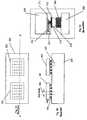
- FIG. 3Ashows two chips 301 and 302 flipped upside down and placed on a ceramic substrate 303 with a plated interconnect (not shown).
- FIG. 3Bis a sectional view along section AA′ of FIG. 3A .
- Balls 304 on the chips 301 , 302are placed on metal or copper posts 305 on the substrate 303 .
- the balls 304are soldered or fused to the posts 305 .
- the posts 305have a pitch 306 .
- FIG. 3Cis an enlarged view of an area 307 of FIG. 3B .
- a ceramic substrate 308has a copper post 309 that connects to another post (not shown) through copper plated multilevel wiring, as known in the art.
- Silicon substrate 310supports an insulation layer 311 .
- a metal connection 312is covered by an insulator layer 313 , which has a contact hole 314 .
- Another metal connection 315may be formed of copper or gold, for example, and is placed on top of the contact hole 314 .
- a metal semi-hemispheric ball 316is placed or otherwise set on the metal connection 315 .
- the chip 301 and substrate 308are aligned so that the ball 316 is on top of the post 309 .
- the ball 316is soldered or fused to the post 309 . Once soldered, the BGA assembly of two interconnected chips 301 and 302 and the substrate 303 is complete.
- the pitch 306 of the posts 305determines connectivity of the BGA.
- State of the art pitch ‘p’is 4 mil or 100 microns.
- the connectivity ‘C’is defined as a maximum number of wires that can connect two chips 301 and 302 . C is equal to 1/p 2 , which is 1E04/cm 2 for BGA's.
- connectivity of a state of the art silicon chipis significantly larger. In a silicon chip, if a feature size of a CMOS process is ‘F’, then the number of via connections on the top layer of the chip determines the connectivity of the chip.
- the connectivity C for a chipis 1/(2F 2 ). For a state of the art CMOS process, the feature size F is 100 nm. So the maximum connectivity for a chip is 1E12/cm 2 .
- the gap between the connectivity of a BGA and that of a chipis very large.
- the capacitances at the output of the BGA, ceramic substrate posts and plated interconnectsare very high and cause significant delay in signals going from one chip 301 to another 302. These delays limit the clock rate ‘f’ at which signals can travel between logic and memory chips.
- the best clock rate possible for BGA'sis 100 MHz at commonly used TTL signal levels as compared to clock rates ‘f’ of 1 GHz within a 90 nm CMOS chip.
- f chipis a clock rate possible in a within a chip (e.g., 4 GHz in 100 nm CMOS),
- C chipis connectivity within a chip (e.g., 1E12/cm 2 ),
- f BGAis clock rate possible within a BGA assembly (e.g., 100 MHz), and
- C BGAis connectivity of a BGA assembly (e.g., 1E04/cm 2 ).
- ratio R1E08.
- Such a high ratiocan open up many areas of applications, which are not possible today through the use of BGA technology or other chip interconnect technologies.
- the principles of the present inventionprovide for self-alignment structures, such as micro-balls and V-grooves, to be formed on chips made by different processes.
- the self-alignment structuresmay be aligned to mask layers within an accuracy of one-half the smallest feature size inside a chip.
- the alignment structurescan align an array of pads having a pitch of 0.6 microns, compared to a pitch of 100 microns available with today's Ball Grid Array (BGA) technology.
- BGABall Grid Array
- clock rates between interconnected chipscan be increased from 100 MHz to 4 GHz due to low capacitance of the interconnected pads.
- chipscan be made smaller, thereby reducing cost of chips by order(s) of magnitude.
- One embodimentincludes a first chip formed by a first process and a second chip formed by a second process.
- the first chipmay include first conductive pads and first alignment structure(s).
- the second chipmay include second conductive pads and second alignment structure(s).
- the first and second alignment structure(s)may be positionally aligned, thereby causing at least a subset of the first and second conductive pads to be aligned.
- Another embodimentmay include an electronic chip, including a substrate, an electronic circuit formed on the substrate, and conductive pads formed on the substrate and connected to the electronic circuit.
- the conductive padsmay have a pitch less than approximately 100 microns.
- an electronic chipmay include a substrate, an electronic circuit formed on the substrate, and conductive pads formed on the substrate and connected to said electronic circuit, said conductive pads covering a surface area less than approximately 10 square microns on the substrate.
- a method of manufacturing a chipmay include forming (i) first electrical components, (ii) a plurality of first conductive pads, and (iii) at least one first alignment structure on a first substrate using a first chip manufacturing process.
- the first alignment structure(s)may be arranged to be aligned with at least one second alignment structure on a second substrate having second conductive pads disposed thereon by a second chip manufacturing process.
- a method for aligning a first and second chipmay include contacting at least one first self-alignment feature of a first chip with at least one second self-alignment feature of a second chip.
- the first and second chipsmay be moved relative to each other to enable the first and second self-alignment feature(s) to self-align.
- Another embodimentmay include a method of aligning a first chip with a second chip, including positioning a first chip including first alignment feature(s) and first conductive pads, positioning a second chip including second alignment feature(s) and second conductive pads, and moving at least one of the first and second chips relative to the other chip to align the first and second alignment feature(s) to cause at least a subset of the first and second conductive pads to be aligned.
- Another embodimentmay include a method of communicating signals between chips, including communicating electrical signals between a first and second chip, the electrical signals may pass from a first conductive pad disposed on the first chip to a second conductive pad disposed on the second chip, where the first and second conductive pads are bonded together.
- FIG. 1Ais the top view of a chip with state of the art Flip Chip technology
- FIG. 1Bis a sectional view of the chip in FIG. A along section AA′;
- FIG. 2Ais a top view of an enlarged area 103 of an interconnect metal of the chip
- FIG. 2Bis the view of the enlarged area of FIG. 2A showing details of a layout of the interconnect metal
- FIG. 3Ais the top view of two chips packaged on a ceramic substrate using Flip Chip technology
- FIG. 3Bis the sectional view of the two chips packaged on the ceramic substrate of FIG. 3A using Flip Chip technology along the section AA′;
- FIG. 3Cis detailed section of view of an area of FIG. 3B showing detail of a connection between one of the chips mounted on the ceramic substrate of FIG. 3A using Flip Chip technology;
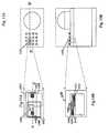
- FIG. 4Ais top view of a first chip with four holes etched in it according to an embodiment of the present invention after wafer processing is complete;
- FIG. 4Bis a sectional view of the first chip in FIG. 4A along a section AA′ illustrating a “V” groove formed using an anisotropic etching process according to an embodiment of the present invention
- FIG. 5Ais the top view of a second chip with four pads arranged corresponding to the four holes of the first chip of FIGS. 4A and 4B ;
- FIG. 5Bis a sectional view of the second chip in FIG. 5A along a section AA′ illustrating a semi-hemispheric ball 503 constructed on the pad;
- FIG. 6Ais a top view of an assembly of the first chip of FIGS. 4A and 4B and the second chip of FIGS. 5A and 5B with the semi-hemispheric ball self-aligned and well-centered in the V-grooves according to an embodiment of the present invention
- FIG. 6Bis a sectional view of the assembly of FIG. 6A along section AA′ illustrating balls self-aligned to V-grooves;
- FIG. 7Ais top view of the first chip of FIG. 4A with four holes etched in it after wafer processing is complete according to an embodiment of the present invention
- FIG. 7Bis a sectional view of the first chip of FIG. 4A along a section AA′ illustrating a V-groove formed using an anisotropic etch process
- FIG. 8Ais an enlarged view of an area of FIG. 7A illustrating details of a position of the V-groove with respect to internal via posts of a chip in which the V-groove is aligned to a via post with an accuracy of 0.5F, where F is equivalent to the smallest features on a chip;
- FIG. 8Bis an enlarged view of an area of FIG. 7B and a sectional view along section BB′ of 8 A;
- FIG. 9Ais an enlarged view of an area 703 of FIG. 7A illustrating details of a position of the V-groove 802 with respect to the internal via posts 803 of a chip in which the V-groove 802 is aligned to the internal via posts 803 with an accuracy of 0.5F, where F is the smallest features on a chip;
- FIG. 9Bis an enlarged view of an area 704 of FIG. 7B and a sectional view along section AA′ of FIG. 9A ;
- FIG. 10Ais an enlarged view of an area 902 of FIG. 9A illustrating details of a multilevel interconnect inside the chip and top post to be connected to a second chip;
- FIG. 10Bis the enlarged area 904 of FIG. 9B showing details of the multilevel interconnect and top post to be connected to a second chip;
- FIG. 11Ais the top view of a second chip with four pads arranged to be connected to the V-grooves of the first chip of FIG. 9A ;
- FIG. 11Bis a sectional view of the second chip of FIG. 11A along section AA′;
- FIG. 12Ais an enlarged view of an area 1101 on the second chip of FIG. 11A showing the position of a round pad 1201 and a post 1202 in which the pad and the post are self-aligned with accuracy of 0.5F, where F is the minimum feature size in a chip;
- FIG. 12Bis an enlarged view of an area 1102 showing a semi-hemispheric ball 1204 coupled to the pad 1203 and the posts inside the second chip of FIG. 11A ;
- FIG. 13Ais an enlarged view of the same area as illustrated in FIG. 12A ;
- FIG. 13Bis an enlarged view of the same area as FIG. 12B ;
- FIG. 14Ais an enlarged view of an area 1301 of FIG. 13A showing details of a multilevel interconnect inside the chip and a top post to be connected to a second chip;
- FIG. 14Bis an enlarged view of an area 1302 of FIG. 13B showing details of a multilevel interconnect and top post to be connected to a second chip;
- FIG. 15Ais a top view of an assembly of a first chip mounted on a second chip, similar to the assembly of FIG. 6A ;
- FIG. 15Bis a sectional view of the assembly of FIG. 15A similar to the assembly of FIG. 6B ;
- FIG. 16Ais an enlarged view of an area 1503 of FIG. 15A showing self-aligned first and second chip
- FIG. 16Bis an enlarged view of an area 1504 of FIG. 15B showing perfect alignment of a ball and groove and, consequently, perfect alignment of posts on two chips;
- FIG. 17is a profile view of the two chips of FIG. 15B in a face-to-face surface arrangement
- FIG. 18Ais an enlarged first profile view of surfaces with rough alignment of a ball and V-groove
- FIG. 18A-1is a diagram of the position of the posts on both chips when the balls are just inside an edge of the V-grooves;
- FIG. 18Bis a second profile view in the middle of a slide of the balls along a sloping surface of the V-grooves;
- FIG. 18B-1is a diagram of an alignment of posts in motion as the ball slides along the sloping surface of the V-groove;
- FIG. 18Cis a third profile view illustrating a self aligned position of the balls in the V-grooves
- FIG. 18C-1is a diagram illustrating aligned posts as the balls are in a final position in the V-grooves
- FIG. 19Ais same as FIG. 6A ;
- FIG. 19Bis same as FIG. 6B ;
- FIG. 20Ais a diagram illustrating an enlarged area of FIG. 19A and a mating pillar
- FIG. 20Bis a diagram illustrating an enlarged area of FIG. 19B and showing a cross-section of a pillar and mating posts, where the posts on the two chips are aligned when the pillar has completed sliding along the slope of V-groove and arrived at a final position;
- FIG. 21is a diagram illustrating the profile of surfaces of the faces of the two chips
- FIG. 22Ais a diagram illustrating an enlarged profile of surfaces of FIG. 21 when a pillar is just inside a V grove;
- FIG. 22A-1is a diagram that shows a degree of misalignment of posts of two chips
- FIG. 22Bis a diagram that shows the profiles in the middle of a slide of a pillar along a sloping surface of a V-groove
- FIG. 22B-1is a diagram that shows alignment of two chips in motion
- FIG. 22Cis a diagram that shows a pillar in a final position and posts in perfect alignment at an end of motion
- FIG. 22C-1is a diagram illustrating aligned posts as the pillars are in a resting position in The V-grooves.
- FIG. 23Ais an assembly of two chips and, where both chips have V-grooves, and a micro-ball resides in a cavity formed by two face-to-face V-grooves;
- FIG. 23Bis a diagram illustrating an enlarged area of FIG. 23A that shows a placement of a micro-ball in a V-groove followed by placement of a second chip with its V-groove self-aligned on the ball with posts being self-aligned;
- FIG. 24is a profile diagram of two chips with two grooves, where one of the grooves is a deep groove for initial alignment and at least one other groove is shallow a groove for fine(r) alignment;
- FIGS. 25A and 25Bare illustrations of two chip configurations showing a first chip and second chip being self-aligned
- FIG. 26is a block diagram of an exemplary system including a device having multiple chips being connected;
- FIG. 27is a flow diagram of an exemplary process for aligning two chips.
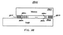
- FIG. 28is a block diagram of an exemplary device formed of a first chip produced by a first process and a second chip produced by a second process.
- An example embodiment of the present inventionmay be used to assemble two silicon chips made with different processes, such as logic and memory (e.g., DRAM, SRAM, or flash) processes, and allow the two chips to have the same connectivity and speed or clock frequency as available in a single chip.
- This assemblyis accomplished by placing one chip on the top of another and aligning them through a self-aligning technique, which has alignment tolerances that are substantially the same as if both chips were fabricated as a single chip. This results in significantly improved connectivity and speed compared to Ball Grid Array (BGA) flip chip techniques.
- BGABall Grid Array
- a set of four square holes in an insulatormay be formed on a first chip after wafer fabrication is complete, using conventional chip photolithography technology, as used to manufacture the chip illustrated in FIG. 4A .
- Thisensures that edges of the holes, which may be shaped as inverted pyramids, are aligned with metal internal interconnect patterns on the chip with an alignment tolerance that is substantially the same as interlayer tolerances inside the chip.
- an anisotropic etching solutionsuch as potassium hydroxide (KOH)
- KOHpotassium hydroxide
- siliconis etched to form the holes, such as described in “Single-mask micro fabrication of aspherical optics using KOH anisotropic etching of Silicon,” D. W. de Lima Monteiro, O. Akhzar-Mehr, P. M. Sarro and G Vdovin Electronic Instrumentation Laboratory, Delft University of Technology, Mekelweg 4, 2628 CD Delft, The Netherlands, the entire teachings of which are incorporated herein by reference.
- KOHKOH
- etching processproduces inverted pyramids and cubes depending on crystal orientation of the silicon.
- Other etching compoundsmay be used in the etching process as understood in the art.
- the sides of the etched inverted pyramidsare substantially flat due to anisotropic etching, which etches in a certain plane ⁇ 111> or ⁇ 110> in this case and not in ⁇ 100>.
- the sidesin fact, become polished similar to the top surface of the substrate in which the hole is etched.
- V-groovesmay be used because the shape is naturally etched into silicon and the shape is substantially symmetrical, thereby providing for self-alignment and described further herein.
- the shape of the holemay be formed as an inverted pyramid that, in a sectional view, looks like a V-groove, as illustrated in FIG. 4B .
- Sets of four semi-hemispheric ballsare formed on a second chip, at the end of wafer processing, using a similar process as used in Flip Chip or Ball Grid Array (BGA) technology (e.g., U.S. Pat. No. 5,424,245) as illustrated in FIGS. 5A and 5B .
- BGABall Grid Array
- the ballsmay alternatively be semi-spherical.
- the shape of the ballis uniform from ball to ball for all the balls on the chip.
- Variation in the diameter of the balls of such an embodimentis expected to be the same as the variation in the size of lithography patterns of metal lines on the chip, which is of the order of 0.5F, where F is a feature size of a photolithography and etch process that is used to form the balls.
- Fis a feature size of a photolithography and etch process that is used to form the balls.
- variation of the diameter of the ballis less than 0.5 micron.
- a second chip with ballsis placed on a first chip with indentations such as V-grooves in a face-to-face arrangement and roughly aligned. Once the balls are in the vicinity of the indentations, the balls slide into respective indentations by gravity as in FIGS. 18A , 18 B, and 18 C.
- FIGS. 19A , 19 B, 20 A and 20 BAnother embodiment of this invention is shown in FIGS. 19A , 19 B, 20 A and 20 B.
- a first chiphas the V-grooves as described above, but a second chip has pillars instead of balls. Pillars are formed using standard silicon technology that includes insulator deposition, photolithography and anisotropic etching of insulator.
- FIG. 20Bshows how the insulator post is positioned in a V-groove at the end of self-aligning the post in the V-groove.
- FIG. 20Balso shows that through the self-alignment process, metal posts at surfaces of both chips get self-aligned to an accuracy of lithography of the process used in fabricating the wafer.
- FIGS. 22A , 22 B and 22 CAn example method of self-aligning is shown in FIGS. 22A , 22 B and 22 C. As illustrated in FIGS. 22A-22C , a top chip with insulator posts is roughly aligned to V-grooves in the bottom chip, and then the top chip is “dropped” on the bottom chip. The posts slide down and settle in a known predetermined position in perfect alignment with the bottom chip. To ensure substantially perfect self-alignment, an ultrasonic vibration may be applied to the chips.
- insulator pillars and V-grooveshave very large dimensions (greater than 100 microns) compared with the metal posts on the chip (less than 100 nm), so that alignment of the insulator post and V-groove can be done in a standard assembly manufacturing line.
- FIGS. 23A and 23BAnother embodiment of this invention is shown in a sectional view of two chips placed on each other, as illustrated in FIGS. 23A and 23B .
- both chipshave a set of four holes with V-grooves, as was done in the first chip in the first embodiment.
- a micro-ball with diameter in the range of 100 microns and a dimension control in the sub-micron rangeis placed in the bottom chip, as illustrated in FIG. 23B .
- There are many methods of placing the ball in the V-groovesuch as passing a large number of balls over the chip until four balls fall naturally into the four V-grooves.
- the second chipis placed over the first chip so that V-grooves in the top and bottom chips are roughly aligned.
- the top chipis allowed to drop so that it slides into a self-aligned position.
- embodiments of this inventionalso reduce the cost of the multi-chip module by reducing the component count from 3 to 2 by eliminating the ceramic substrate.
- FIGS. 4A and 5Aare top views of two fully fabricated silicon chips 401 and 501 ready for packaging.
- Embodiments of this inventionsolve the problem of aligning the faces of two chips as in Flip Chip technology and described in the background section above.
- the problemis the alignment accuracy of two chips.
- alignment accuracy between two chipsis 50 microns.
- the pitch of the padsis 100 microns, which limits the number of pads on a 1 cm 2 chip to 10,000.
- a structure and method of aligning two chipssuch as chips 401 as in FIGS. 4A and 4B and 501 as in FIGS. 5A and 5B , face-to-face as in the combination of chips 601 of FIGS. 6A and 6B .
- An alignment accuracysubstantially the same as aligning mask layers made during a wafer fabrication process, which is usually 0.5F, where F is the minimum feature size of geometric patterns formed on a wafer to form transistors, results.
- the seamless integration processstarts with forming four square holes 402 on a first chip 401 .
- the holes 402are inverted pyramids that appear like a V-groove 403 in a sectional view of the first chip shown in FIG. 4B .
- the holes 402may be formed using chip fabrication technology to ensure alignment of the edge of the holes or V-grooves to the metal patterns (not shown) inside the chip as accurately as other mask alignments during the wafer fabrication process.
- FIG. 5Ais a top view of four semi-hemispheric balls 502 formed on a second chip 501 .
- FIG. 5Bshows a section view of the second chip 501 and ball 503 from among the semi-hemispheric balls 502 .
- the ball 502may be formed using the same process as used in forming Ball Grid Arrays or BGA's. Alignment of the balls 502 to the metal patterns inside the chip 501 is thus substantially as accurate as the alignment accuracy of mask layers used during the fabrication of the wafer from which the chip 501 is made. If F is the minimum feature size in wafer processing, alignment accuracy of 0.5F can be obtained by the ball/V-groove arrangement.
- FIG. 6Ais a top view of an assembly of the first chip 401 of FIGS. 4A and 4B and the second chip 501 of FIGS. 5A and 5B , indicated as chip 602 of the chips 601 , with the semi-hemispheric ball 603 self-aligned and well centered in the V-grooves 604 according to an embodiment of the present invention.
- a second chip 607is aligned roughly face-to-face to a first chip 605 so that balls 608 line-up approximately over a V-groove 606 using standard aligning equipment in the packaging facility, which has sub 100 micron alignment accuracy.
- the second chip 607is brought in contact with the first chip 605 and allowed to self-align itself by the balls 608 sliding along the surface of the V-grooves 606 and stopping when the balls 608 are touching all four surfaces of the V-grooves 606 .
- aligning equipmentwhich may include sonic vibration equipment, aligns the balls with an accuracy of 100 microns
- self-alignment of the balls 608 to the V-grooves 606allows for aligning accuracy for conductive pads (see FIG. 16B ) the same as that of the V-grooves 606 to the internal metal patterns (not shown) on the first chip 605 and the balls 608 to the internal metal patterns (not shown) of second chip 607 .
- the balls 608 and V-grooves 606are not conductive, but, rather, provide for agreement between the chips.
- the materials for the ballsmay include glass or other insulation material.
- FIGS. 7A and 7Bare the same as FIGS. 4A and 4B with respect to similar reference numbers described above in the latter figures.
- FIGS. 8A and 8Bare enlarged views of areas 703 and 704 of FIGS. 7A and 7B , respectively.
- FIG. 8Ais a top view of a first chip 801 illustrating a hole 802 defined within a top layer 804 .
- the first chip 801also includes posts 803 over metal lines (not shown) inside the chip 801 with minimum geometry. If the same equipment is used to align the hole 802 to the posts 803 as is used to align other mask layers, then the hole 802 is aligned to the posts 803 with the same accuracy.
- FIG. 8Bis a sectional view of FIG. 8A .
- An insulator 804i.e., the top layer
- a silicon layer 805is formed (e.g., deposited) on a silicon layer 805 .
- a substantially square or other geometric shaped hole 802is defined in the insulator 804 through anisotropic etching techniques.
- the silicon layer 805is etched to form the hole 806 using an anisotropic etch solution, such as KOH.
- the etchingforms the V-groove 806 and stops as understood in the art and as described in “Single-Mask Micro Fabrication of a Spherical Optics Using KOH Anisotropic Etching of Silicon,” D. W. de Lima Monteiro, O. Akhzar-Mehr, P. M.
- V-groove 806is fixed by the crystal orientation of the silicon in the silicon layer 805 .
- a typical angle of the slopeis 54.75°, as described in de Lima Monteiro et al.
- the posts 803 and 807are formed during the wafer fabrication process during multilevel metal depositions and etchings.
- FIGS. 9A and 9Bare same as FIGS. 8A and 8B .
- FIGS. 10A and 10Bare enlarged top and profile views, respectively, illustrating areas 902 and 904 of FIGS. 9A and 9B , respectively.
- FIG. 10Ashows details of the area 902 surrounding a post or conductive pad (interchangeably used herein) 803 of FIG. 9A .
- FIG. 10Bshows details of a sectional view of section AA′ of FIG. 10A of a multilevel interconnect 1013 below a post 1002 corresponding to the post 803 in FIG. 9A .
- Three levels of metals with two viasare shown in FIGS. 10A and 10B . In FIG.
- FIG. 10Ashows a sectional view along the section AA′ of FIG. 10A .
- reference number 1008references a third metal
- reference number 1009references a second via
- reference number 1010references a second metal
- reference number 1011references a first via and reference number 1012 references a first metal.
- vias and postsmay be the same and made with either tungsten or copper using a chemical mechanical planarization (CMP) process.
- CMPchemical mechanical planarization
- a CMP processcan be used to deposit metal or an insulator on an uneven surface and planarize it using chemical and mechanical polishing techniques.
- FIGS. 11A and 11Bare top and sectional views of a second chip.
- FIGS. 12A and 12Bare enlarged views of areas 1101 and 1102 of FIGS. 11A and 11B , respectively.
- FIG. 12Ashows a ball 1201 aligned a distance d from a post 1202 using wafer fabrication alignment tools. The misalignment of the ball 1201 to the post 1202 is 0.5F, where F is the minimum feature size of geometric patterns formed on the wafer to form transistors.
- FIG. 12Bconstruction of the ball 1201 of FIG. 12A is shown, where a hemispherical section 1204 is constructed or adhered to a round pad 1203 formed on an insulator 1205 .
- the round pad 1203may be a composite layer of tungsten gold and lead-tin or other similar metals. In one embodiment, by heating the wafer, lead-tin forms a perfect semi-sphere, which may be a hemisphere.
- FIGS. 13A and 13Bare the same as FIGS. 12A and 12B , respectively.
- FIGS. 14A and 14Bare enlarged views of areas 1301 and 1302 of FIGS. 13A and 13B , respectively.
- FIGS. 14A and 14Billustrate an example of multilevel metal interconnect inside a second chip (e.g., the second chip 607 of FIG. 6A ).
- reference number 1401references a ball
- reference number 1402references a third metal
- reference number 1403references a second via
- reference number 1404references a second metal
- reference number 1405references a first via
- reference number 1406references a first metal.
- reference number 1407references a ball
- reference number 1408references a third metal
- reference number 1409references a second via
- reference number 1410references a second metal
- reference number 1411references a first via and reference number 1412 references a first metal.
- FIG. 16A and FIG. 16Bare enlarged views of areas 1503 and 1504 of FIGS. 15A and 15B , respectively, which are the same as FIGS. 6A and 6B , respectively, after a second chip 1502 is placed over a first chip 1501 .
- a ball 1602 coupled to the second chip 1502is guided by the sloping sidewall of the V-groove 1601 into a self-aligned position.
- FIG. 17is enlarged in FIGS. 18A-18C .
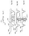
- FIG. 18Atwo surfaces 1801 and 1802 are roughly aligned.
- This rough alignment processmay be performed using conventional or custom equipment to position the first and second surfaces 1801 and 1802 with very little space between them (e.g., less than 100 nm).
- Such a positioning processis commonly performed in chip manufacturing with the aid of a microscope.
- Area 1805 A in FIG. 18Ais enlarged in 1805 AA of FIG. 18A-1 , which shows posts 1807 on the first chip and posts 1808 on the second chip.
- the ball 1803Once the ball 1803 is inside the V-groove 1804 , it slides down to a resting position, as illustrated in FIGS. 18B and 18C .
- 18A-1 , 18 B- 1 and 18 C- 1show posts or conductive pads 1807 and 1808 come to a substantially aligned position within an accuracy of 0.5F, where F is the smallest feature size inside a chip.
- upper posts 1808are several microns misaligned from lower posts 1807 .
- the postsare substantially self-aligned as a result of a mating between the balls and V-grooves.
- An ultrasonic vibrationmay also be applied to the chips to further cause the chips to self-align. If the chips are placed together with an accuracy of 10 microns, then movement between the chips using vibration or otherwise may be a maximum of 5 microns or less.
- the vibrationsIn the case of using gravity in the self-alignment process, the vibrations, if used, cause the balls 1803 top chip to slide to the bottom of the V-grooves 1804 , which causes the posts 1808 and 1807 to slide and contact one another. Heating the two chips to bond the metal posts completes assembly of the two chips.
- Metallike copper, bonds or fuses around 400° C. Other bonding techniques, such as chemical bonding or heat and pressure, may be utilized to cause the metal posts (i.e., conductive pads) to bond.
- FIGS. 19A-22CA second embodiment of the invention is shown in FIGS. 19A-22C .
- a second chip 1902is placed over a first chip 1901 , as in the top view in FIG. 19A and the sectional view in FIG. 19B .
- FIGS. 20A and 20Bare enlarged views of areas 1903 and 1904 , respectively.
- Construction of the first chip 1901is the same as described earlier in reference to FIGS. 7 , 8 , 9 and 10 .
- Construction of the second chip 1902is shown in FIGS. 20A and 20B .
- a thick layer of glass 2004is deposited over the wafer surface 2003 .
- a tall cylindrical pillar 2005is etched with a diameter smaller than the width of the V-groove 2001 .
- the height of pillar 2005is determined by the depth of the groove 2001 , the thickness of the insulators 2006 , 2003 , and the height of posts 2007 .
- a pillar having a circular shapeit should be understood that any shape, such as a square, oval, octagonal or otherwise, that enable the chips to self-align may be utilized.
- FIG. 21Surface profiles 2101 and 2102 of the two chips 1901 and 1902 of FIG. 19 are shown in FIG. 21 .
- an outline of two surfaces 2101 , 2102 that face each other as shown in FIG. 21 at their final resting positionsare enlarged in FIGS. 22A-22C to show different respective positions.
- FIG. 22Athe two surfaces 2201 and 2202 are roughly aligned.
- An area 2205 in FIG. 22Ais enlarged in area 2206 of FIG. 22A-1 , which shows posts 2207 on the first chip 2101 and the posts 2208 on the second chip 2102 .
- the pillar 2204Once the pillar 2204 is inside the V-groove 2203 , it slides down to a resting position, as illustrated in FIGS. 22B and 22C .
- FIGS. 22A-1 , 22 B- 1 and 22 C- 1show the posts 2207 and 2208 come to a substantially aligned position within an accuracy of 0.5F, where F is the smallest feature size inside a chip.
- posts 2208are several microns misaligned from posts 2207 .
- the posts 2207 and 2208are substantially self-aligned. Heating the two chips 2101 and 2102 to bond the metal posts 2208 may complete assembly of the two chips 2101 and 2102 . Metal, like copper, bonds around 400° C.
- FIGS. 23A and 23BA third embodiment of the present invention is shown in FIGS. 23A and 23B .
- a first chip 2301 and a second chip 2302are constructed in the same way as described in reference to FIGS. 7 , 8 , 9 and 10 .
- the V-grooves 2303 and 2304are 100 microns wide.
- a spherical micro-ball 2305made with any suitable metal or glass, is placed inside the groove 2303 of the first chip 2301 .
- the diameter of the ball 2305is smaller than the size of the V-groove 2303 .
- One of the methods of placing balls 2305 in the grooves 2303may include flooding the surface of the first chip 2301 with many micro-balls until four grooves on the first chip 2301 are filled.
- the grooves on the first chip 2301may be filled with balls for the self-alignment process to operate in accordance with this embodiment of the present invention.
- the second chip 2302is roughly aligned to the first chip 2301 so that the micro-ball 2305 is slightly inside the V-groove 2304 in the second chip 2302 . As the second chip 2302 is lowered, by gravity in one embodiment, it is guided by the surface of V-groove 2304 until it arrives at a final resting position.
- the second chip 2302is self-aligned to the first chip 2301 within the accuracy of the diameter of the micro-ball. For example, if the diameter can be controlled within 1 micron, then the accuracy of alignment is 1 micron.
- the V-grooves 2303 and 2304are aligned to the posts 2306 and 2307 , respectively, by using state of the art chip fabrication methods, such as masking, photolithography, and etching of insulators and silicon.
- state of the art silicon fabrication methodsenable alignment accuracy of 100 nm today.
- misalignment of the posts 2306 and 2307 on the first and second chips 2301 and 2302is limited by the accuracy of the ball diameter tolerance. Balls with sub-micron accuracy are available today commercially.
- a fourth embodimentis shown in FIG. 24 .
- a first chip 2401 and second chip 2402are the pair of chips face-to-face with two alignment pillars 2403 and 2405 , having different diameters, on the first (top) chip 2401 , as well as two (wide and narrow) alignment grooves 2404 and 2406 corresponding to the two aligned pillars 2403 and 2405 and on the second (bottom) chip 2402 .
- This stage of alignmentis noted as a first stage 2407 .
- the wide pillar 2403is on the top of the wide groove 2404 , though it may be not be in right in the center of the groove as in the first stage 2407 .
- the first chip 2401is lowered until it touches the second chip 2402 .
- the first chip 2401is released to slide on its own towards the center of the wide groove 2404 until the narrow pillar 2405 touches the surface of the first chip 2401 .
- sliding of the wide pillar 2403stops.
- the first chip 2401is pushed to the right along a plane until the narrow pillar 2405 is inside the narrow groove 2406 .
- the fourth stage 2410the first chip 2401 starts sliding again until the narrow pillar 2405 is right in the middle of the narrow V-groove 2406 , as illustrated in a fifth stage 2411 .
- the wide pillar 2403does not touch the sides of the V-groove 2044 due to tolerance limitations.
- This exampleshows that the purpose of the narrow pillar 2405 and groove 2406 along with the wide pillar 2403 and groove 2404 is to increase the alignment accuracy in the event surfaces of wide grooves are not well controlled.
- the other pillar and V-groove interactions and post contactsmaintain the two chips 2401 and 2402 in a substantially horizontal orientation.
- a fifth embodimentis also contemplated where a top chip and bottom chip have two wide V-grooves and two narrow V-grooves.
- the bottom chipmay be flooded with small and large balls to fit inside wide and narrow grooves.
- the top chipis aligned over the bottom chip roughly using existing tools and lowered until the wide grooves touch large balls and start sliding downwards until the surface of the narrow V-grooves of the top chip touches the small balls. At that point, the top chip is pushed laterally along a plane until the small balls are inside the small grooves of the top chip and starts sliding again until the small balls are in the center of the narrow grooves of the bottom chip.
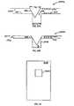
- FIGS. 25A and 25Bare illustrations of two chip configurations 2500 a showing a first chip 2502 and second chip 2504 being self-aligned.
- the second chipincludes a pyramid structure 2506 deposited on or etched to extend from a surface of the first chip 2502 and the first chip 2504 includes an indentation 2508 in the form of a cube, rectangle, or other shape that enables the pyramid structure 2506 to self-align with the indentation 2508 .
- the indentationhas a width w
- the pyramid structure 2506has a base width w 2 so that the pyramid structure 2506 slides into the indentation 2508 , but does not touch the apex of the pyramid structure to the second chip 2504 .
- First conductive pads 2510 on the first chip 2502 and second conductive pads 2512 on the second chip 2504are configured in pitch and height such that the first and second conductive pads 2510 and 2512 contact one another when the pyramid structure 2506 is self-aligned with the indentation 2508 . As shown, there is a height h between the apex of the pyramid structure 2506 and second chip 2504 . It should be understood that first and second chips 2502 and 2504 could be reversed in position.
- FIG. 26is a block diagram of an exemplary system 2600 including a device 2602 having multiple chips being connected using the principles of the present invention.
- the system 2600may be any system that can integrate the device 2602 .
- the systemmay be a computing device (e.g., computer, calculator), communication device (e.g., mobile wireless device, modem), gaming device (e.g., handheld game, video game), automobile component (e.g., controller), or any other system.
- a computing devicee.g., computer, calculator
- communication devicee.g., mobile wireless device, modem
- gaming devicee.g., handheld game, video game
- automobile componente.g., controller
- FIG. 27is a flow diagram of an exemplary process 2700 for aligning two chips.
- the self-alignment process 2700starts at step 2702 .
- at least one first self-alignment feature of a first chipmay be contacted with a second chip having at least one second self-alignment feature.
- the self-alignment featuresmay be any features, including indentations (e.g., inverted pyramid) and protrusions (e.g., semi-spherical ball, circular pillar), which enable the features to self-align when placed together.
- gravityassists in performing the self-alignment between the at least one first and second alignment features.
- the first and second chipsare moved relative to each other to enable the at least one first and second self-alignment features to self-align.
- the movementmay be performed horizontally or in a planar motion. Additionally and/or alternatively, the movement may include applying a vibration, such as an ultrasonic vibration, to cause the at least one first and second self-alignment features to self-align.
- the self-alignment process 2700ends at step 2708 .
- FIG. 28is a block diagram of an exemplary device 2800 formed of a first chip 2802 produced by a first process and a second chip 2804 produced by a second process.
- the first chip 2802is a logic chip and the second chip 2804 is a memory chip.
- the first chip 2802includes first conductive pads 2806 a - 2806 n (collectively 2806 ) and the second chip 2802 includes second conductive pads 2808 a - 2808 n (collectively 2808 ).
- the first conductive pads 2806 and second conductive pads 2808are aligned using self-alignment features 2810 (e.g., pillars that align with V-grooves (not shown)) and bonded together by a heat process.
- self-alignment features 2810e.g., pillars that align with V-grooves (not shown)
- the first chip 2802communicates electrical signals 2812 with the second chip 2804 via the bonded first and second conductive pads 2806 and 2808 .
- a logic chipmay communicate electrical signals with a memory chip to store and retrieve data.
- the electrical signalsmay be digital or analog depending on the technology of the chips that are connected together.
- the first chip 2802may be adapted to work with different chip types.
- the first chip 2802may be a logic chip, such as a processor, that can work with different types of memory chips, such as DRAM, SRAM, flash, or other types of memory. Because these different memories may have different communication protocols, each of the memory chips may have a different configuration of the conductive pads so that the logic chip may automatically detect which type of memory chip is connected thereto and adapt the communication protocol for that specific memory chip.
- two conductive padsmay be used for indicating the memory type.
- the indicationsmay be in the form of high logic signals, low logic signals, capacitance, inductance, short signal, or other forms of static or dynamic electronic programming means known in the art.
- These two conductive padsmay provide for four different memory types depending on the inputs (e.g., ‘00’ is DRAM, ‘01’ is SRAM, ‘11’ is flash, and ‘10’ is EEPROM).
- the memorymay include data stored in memory registers that the logic reads to determine the type of memory to which it is connected. It should be understood that the same type of automatic detection of device connections may be performed with other types of chips.
- the conductive pads for the different chipshave different number of connections such that a different subset of the conductive pads of the first chip 2802 are connected to conductive pads on the second chip 2804 depending on the type of the second chip. It is contemplated that a standard interconnect pattern may be developed for the interconnection between different chip types (e.g., logic and DRAM, logic and SRAM, logic and flash, and so forth).
- any of the aforementioned techniquesmay be used in any electronics application, such as computers, mobile phones, wireless devices, calculators, automobile electronics, general or application specific processors, and so forth.
- any electronics applicationsuch as computers, mobile phones, wireless devices, calculators, automobile electronics, general or application specific processors, and so forth.
- specific embodimentshave been shown and described, alternative embodiments for self-aligning two chips with the tolerances described herein in accordance with the principles of the present may be utilized. For example, instead of relying on gravity, the two chips may be vertically arranged and moved together through use of sensitive robotics.
Landscapes
- Engineering & Computer Science (AREA)
- Microelectronics & Electronic Packaging (AREA)
- Power Engineering (AREA)
- Computer Hardware Design (AREA)
- Physics & Mathematics (AREA)
- Condensed Matter Physics & Semiconductors (AREA)
- General Physics & Mathematics (AREA)
- Internal Circuitry In Semiconductor Integrated Circuit Devices (AREA)
Abstract
Description
R=(fchip×Cchip)/(fBGA×CBGA),
Claims (21)
Priority Applications (3)
| Application Number | Priority Date | Filing Date | Title |
|---|---|---|---|
| US11/508,007US8957511B2 (en) | 2005-08-22 | 2006-08-21 | Apparatus and methods for high-density chip connectivity |
| PCT/US2006/032592WO2007024774A2 (en) | 2005-08-22 | 2006-08-22 | Apparatus and methods for high-density chip connectivity |
| US14/593,994US20150162293A1 (en) | 2005-08-22 | 2015-01-09 | Apparatus And Methods For High-Density Chip Connectivity |
Applications Claiming Priority (2)
| Application Number | Priority Date | Filing Date | Title |
|---|---|---|---|
| US70989605P | 2005-08-22 | 2005-08-22 | |
| US11/508,007US8957511B2 (en) | 2005-08-22 | 2006-08-21 | Apparatus and methods for high-density chip connectivity |
Related Parent Applications (1)
| Application Number | Title | Priority Date | Filing Date |
|---|---|---|---|
| US11/507,888ContinuationUS7745301B2 (en) | 2005-08-22 | 2006-08-21 | Methods and apparatus for high-density chip connectivity |
Related Child Applications (1)
| Application Number | Title | Priority Date | Filing Date |
|---|---|---|---|
| US14/593,994ContinuationUS20150162293A1 (en) | 2005-08-22 | 2015-01-09 | Apparatus And Methods For High-Density Chip Connectivity |
Publications (2)
| Publication Number | Publication Date |
|---|---|
| US20070194416A1 US20070194416A1 (en) | 2007-08-23 |
| US8957511B2true US8957511B2 (en) | 2015-02-17 |
Family
ID=38427342
Family Applications (2)
| Application Number | Title | Priority Date | Filing Date |
|---|---|---|---|
| US11/508,007Expired - Fee RelatedUS8957511B2 (en) | 2005-08-22 | 2006-08-21 | Apparatus and methods for high-density chip connectivity |
| US14/593,994AbandonedUS20150162293A1 (en) | 2005-08-22 | 2015-01-09 | Apparatus And Methods For High-Density Chip Connectivity |
Family Applications After (1)
| Application Number | Title | Priority Date | Filing Date |
|---|---|---|---|
| US14/593,994AbandonedUS20150162293A1 (en) | 2005-08-22 | 2015-01-09 | Apparatus And Methods For High-Density Chip Connectivity |
Country Status (1)
| Country | Link |
|---|---|
| US (2) | US8957511B2 (en) |
Cited By (1)
| Publication number | Priority date | Publication date | Assignee | Title |
|---|---|---|---|---|
| US20150260929A1 (en)* | 2012-09-27 | 2015-09-17 | Fujikura Ltd. | Optical module |
Families Citing this family (5)
| Publication number | Priority date | Publication date | Assignee | Title |
|---|---|---|---|---|
| US7745301B2 (en) | 2005-08-22 | 2010-06-29 | Terapede, Llc | Methods and apparatus for high-density chip connectivity |
| US8957511B2 (en) | 2005-08-22 | 2015-02-17 | Madhukar B. Vora | Apparatus and methods for high-density chip connectivity |
| US8076178B2 (en)* | 2007-09-28 | 2011-12-13 | Oracle America, Inc. | Self-assembly of micro-structures |
| KR101902566B1 (en) | 2017-07-25 | 2018-09-28 | 엘지디스플레이 주식회사 | Light emitting diode display apparatus and manufacturing method of the same |
| US20230378081A1 (en)* | 2022-05-23 | 2023-11-23 | International Business Machines Corporation | Multi-chip die alignment |
Citations (174)
| Publication number | Priority date | Publication date | Assignee | Title |
|---|---|---|---|---|
| US3401126A (en) | 1965-06-18 | 1968-09-10 | Ibm | Method of rendering noble metal conductive composition non-wettable by solder |
| US3429040A (en) | 1965-06-18 | 1969-02-25 | Ibm | Method of joining a component to a substrate |
| US3458925A (en) | 1966-01-20 | 1969-08-05 | Ibm | Method of forming solder mounds on substrates |
| US3486223A (en) | 1967-04-27 | 1969-12-30 | Philco Ford Corp | Solder bonding |
| US3591839A (en) | 1969-08-27 | 1971-07-06 | Siliconix Inc | Micro-electronic circuit with novel hermetic sealing structure and method of manufacture |
| US3621565A (en) | 1969-06-12 | 1971-11-23 | Nasa | Fabrication of single-crystal film semiconductor devices |
| US3811186A (en) | 1972-12-11 | 1974-05-21 | Ibm | Method of aligning and attaching circuit devices on a substrate |
| US3871015A (en) | 1969-08-14 | 1975-03-11 | Ibm | Flip chip module with non-uniform connector joints |
| US3921285A (en) | 1974-07-15 | 1975-11-25 | Ibm | Method for joining microminiature components to a carrying structure |
| US3988619A (en) | 1974-12-27 | 1976-10-26 | International Business Machines Corporation | Random access solid-state image sensor with non-destructive read-out |
| US3997963A (en) | 1973-06-29 | 1976-12-21 | Ibm Corporation | Novel beam-lead integrated circuit structure and method for making the same including automatic registration of beam-leads with corresponding dielectric substrate leads |
| US4032372A (en) | 1971-04-28 | 1977-06-28 | International Business Machines Corporation | Epitaxial outdiffusion technique for integrated bipolar and field effect transistors |
| UST964009I4 (en) | 1975-02-06 | 1977-11-01 | High voltage semiconductor structure | |
| US4155155A (en) | 1977-01-19 | 1979-05-22 | Alsthom-Atlantique | Method of manufacturing power semiconductors with pressed contacts |
| US4168999A (en) | 1978-12-26 | 1979-09-25 | Fairchild Camera And Instrument Corporation | Method for forming oxide isolated integrated injection logic semiconductor structures having minimal encroachment utilizing special masking techniques |
| US4184043A (en) | 1977-05-02 | 1980-01-15 | U.S. Philips Corporation | Method of providing spacers on an insulating substrate |
| US4322882A (en) | 1980-02-04 | 1982-04-06 | Fairchild Camera & Instrument Corp. | Method for making an integrated injection logic structure including a self-aligned base contact |
| US4374011A (en) | 1981-05-08 | 1983-02-15 | Fairchild Camera & Instrument Corp. | Process for fabricating non-encroaching planar insulating regions in integrated circuit structures |
| US4398338A (en) | 1980-12-24 | 1983-08-16 | Fairchild Camera & Instrument Corp. | Fabrication of high speed, nonvolatile, electrically erasable memory cell and system utilizing selective masking, deposition and etching techniques |
| US4418468A (en) | 1981-05-08 | 1983-12-06 | Fairchild Camera & Instrument Corporation | Process for fabricating a logic structure utilizing polycrystalline silicon Schottky diodes |
| US4425379A (en) | 1981-02-11 | 1984-01-10 | Fairchild Camera & Instrument Corporation | Polycrystalline silicon Schottky diode array |
| US4435790A (en) | 1980-12-24 | 1984-03-06 | Fairchild Camera And Instrument Corporation | High speed, nonvolatile, electrically erasable memory cell and system |
| US4488350A (en) | 1981-10-27 | 1984-12-18 | Fairchild Camera & Instrument Corp. | Method of making an integrated circuit bipolar memory cell |
| US4503598A (en) | 1982-05-20 | 1985-03-12 | Fairchild Camera & Instrument Corporation | Method of fabricating power MOSFET structure utilizing self-aligned diffusion and etching techniques |
| US4512075A (en) | 1980-08-04 | 1985-04-23 | Fairchild Camera & Instrument Corporation | Method of making an integrated injection logic cell having self-aligned collector and base reduced resistance utilizing selective diffusion from polycrystalline regions |
| US4543595A (en) | 1982-05-20 | 1985-09-24 | Fairchild Camera And Instrument Corporation | Bipolar memory cell |
| US4545610A (en) | 1983-11-25 | 1985-10-08 | International Business Machines Corporation | Method for forming elongated solder connections between a semiconductor device and a supporting substrate |
| US4545113A (en) | 1980-10-23 | 1985-10-08 | Fairchild Camera & Instrument Corporation | Process for fabricating a lateral transistor having self-aligned base and base contact |
| US4584594A (en) | 1981-05-08 | 1986-04-22 | Fairchild Camera & Instrument Corp. | Logic structure utilizing polycrystalline silicon Schottky diodes |
| US4617071A (en) | 1981-10-27 | 1986-10-14 | Fairchild Semiconductor Corporation | Method of fabricating electrically connected regions of opposite conductivity type in a semiconductor structure |
| US4622575A (en) | 1981-10-27 | 1986-11-11 | Fairchild Semiconductor Corporation | Integrated circuit bipolar memory cell |
| US4624863A (en) | 1982-05-20 | 1986-11-25 | Fairchild Semiconductor Corporation | Method of fabricating Schottky diodes and electrical interconnections in semiconductor structures |
| US4628339A (en) | 1981-02-11 | 1986-12-09 | Fairchild Camera & Instr. Corp. | Polycrystalline silicon Schottky diode array |
| US4640004A (en) | 1984-04-13 | 1987-02-03 | Fairchild Camera & Instrument Corp. | Method and structure for inhibiting dopant out-diffusion |
| US4757027A (en) | 1983-09-19 | 1988-07-12 | Fairchild Semiconductor Corporation | Method for fabricating improved oxide defined transistors |
| US4762801A (en) | 1987-02-20 | 1988-08-09 | National Semiconductor Corporation | Method of fabricating polycrystalline silicon resistors having desired temperature coefficients |
| US4764480A (en) | 1985-04-01 | 1988-08-16 | National Semiconductor Corporation | Process for making high performance CMOS and bipolar integrated devices on one substrate with reduced cell size |
| US4807021A (en) | 1986-03-10 | 1989-02-21 | Kabushiki Kaisha Toshiba | Semiconductor device having stacking structure |
| US4829363A (en) | 1984-04-13 | 1989-05-09 | Fairchild Camera And Instrument Corp. | Structure for inhibiting dopant out-diffusion |
| US4878611A (en) | 1986-05-30 | 1989-11-07 | American Telephone And Telegraph Company, At&T Bell Laboratories | Process for controlling solder joint geometry when surface mounting a leadless integrated circuit package on a substrate |
| US4908679A (en) | 1981-01-23 | 1990-03-13 | National Semiconductor Corporation | Low resistance Schottky diode on polysilicon/metal-silicide |
| US4947230A (en) | 1984-09-14 | 1990-08-07 | Fairchild Camera & Instrument Corp. | Base-coupled transistor logic |
| US4949148A (en) | 1989-01-11 | 1990-08-14 | Bartelink Dirk J | Self-aligning integrated circuit assembly |
| US4974046A (en) | 1986-07-02 | 1990-11-27 | National Seimconductor Corporation | Bipolar transistor with polysilicon stringer base contact |
| US4982244A (en) | 1982-12-20 | 1991-01-01 | National Semiconductor Corporation | Buried Schottky clamped transistor |
| US5014107A (en) | 1987-07-29 | 1991-05-07 | Fairchild Semiconductor Corporation | Process for fabricating complementary contactless vertical bipolar transistors |
| US5045916A (en) | 1985-01-22 | 1991-09-03 | Fairchild Semiconductor Corporation | Extended silicide and external contact technology |
| US5055418A (en) | 1987-07-29 | 1991-10-08 | National Semiconductor Corporation | Process for fabricating complementary contactless vertical bipolar transistors |
| US5061986A (en) | 1985-01-22 | 1991-10-29 | National Semiconductor Corporation | Self-aligned extended base contact for a bipolar transistor having reduced cell size and improved electrical characteristics |
| US5063168A (en) | 1986-07-02 | 1991-11-05 | National Semiconductor Corporation | Process for making bipolar transistor with polysilicon stringer base contact |
| US5072275A (en) | 1986-02-28 | 1991-12-10 | Fairchild Semiconductor Corporation | Small contactless RAM cell |
| US5098854A (en) | 1984-07-09 | 1992-03-24 | National Semiconductor Corporation | Process for forming self-aligned silicide base contact for bipolar transistor |
| US5100824A (en) | 1985-04-01 | 1992-03-31 | National Semiconductor Corporation | Method of making small contactless RAM cell |
| US5166767A (en) | 1987-04-14 | 1992-11-24 | National Semiconductor Corporation | Sidewall contact bipolar transistor with controlled lateral spread of selectively grown epitaxial layer |
| US5166094A (en) | 1984-09-14 | 1992-11-24 | Fairchild Camera & Instrument Corp. | Method of fabricating a base-coupled transistor logic |
| US5214308A (en) | 1990-01-23 | 1993-05-25 | Sumitomo Electric Industries, Ltd. | Substrate for packaging a semiconductor device |
| US5227316A (en) | 1985-01-22 | 1993-07-13 | National Semiconductor Corporation | Method of forming self aligned extended base contact for a bipolar transistor having reduced cell size |
| US5240511A (en) | 1987-02-20 | 1993-08-31 | National Semiconductor Corporation | Lightly doped polycrystalline silicon resistor having a non-negative temperature coefficient |
| GB2274201A (en) | 1992-12-16 | 1994-07-13 | Deutsche Aerospace | A Method of alignment of semi-conductor plates relative to one another |
| US5340762A (en) | 1985-04-01 | 1994-08-23 | Fairchild Semiconductor Corporation | Method of making small contactless RAM cell |
| US5355035A (en) | 1993-01-08 | 1994-10-11 | Vora Madhukar B | High speed BICMOS switches and multiplexers |
| US5391505A (en) | 1993-11-01 | 1995-02-21 | Lsi Logic Corporation | Active device constructed in opening formed in insulation layer and process for making same |
| US5393712A (en) | 1993-06-28 | 1995-02-28 | Lsi Logic Corporation | Process for forming low dielectric constant insulation layer on integrated circuit structure |
| US5424245A (en) | 1994-01-04 | 1995-06-13 | Motorola, Inc. | Method of forming vias through two-sided substrate |
| US5470801A (en) | 1993-06-28 | 1995-11-28 | Lsi Logic Corporation | Low dielectric constant insulation layer for integrated circuit structure and method of making same |
| US5472901A (en) | 1994-12-02 | 1995-12-05 | Lsi Logic Corporation | Process for formation of vias (or contact openings) and fuses in the same insulation layer with minimal additional steps |
| US5477086A (en) | 1993-04-30 | 1995-12-19 | Lsi Logic Corporation | Shaped, self-aligning micro-bump structures |
| US5494859A (en) | 1994-02-04 | 1996-02-27 | Lsi Logic Corporation | Low dielectric constant insulation layer for integrated circuit structure and method of making same |
| US5498558A (en) | 1994-05-06 | 1996-03-12 | Lsi Logic Corporation | Integrated circuit structure having floating electrode with discontinuous phase of metal silicide formed on a surface thereof and process for making same |
| US5521108A (en) | 1993-09-15 | 1996-05-28 | Lsi Logic Corporation | Process for making a conductive germanium/silicon member with a roughened surface thereon suitable for use in an integrated circuit structure |
| US5539246A (en) | 1995-03-01 | 1996-07-23 | Lsi Logic Corporation | Microelectronic integrated circuit including hexagonal semiconductor "gate " device |
| US5543643A (en) | 1995-07-13 | 1996-08-06 | Lsi Logic Corporation | Combined JFET and MOS transistor device, circuit |
| US5583062A (en) | 1995-06-07 | 1996-12-10 | Lsi Logic Corporation | Self-aligned twin well process having a SiO2 -polysilicon-SiO2 barrier mask |
| US5614428A (en) | 1995-10-23 | 1997-03-25 | Lsi Logic Corporation | Process and structure for reduction of channeling during implantation of source and drain regions in formation of MOS integrated circuit structures |
| US5631581A (en) | 1995-05-10 | 1997-05-20 | Lsi Logic Corporation | Microelectronic integrated circuit including triangular semiconductor "and" gate device |
| US5640049A (en) | 1995-08-18 | 1997-06-17 | Lsi Logic Corporation | Metal interconnect structures for use with integrated circuit devices to form integrated circuit structures |
| US5650653A (en) | 1995-05-10 | 1997-07-22 | Lsi Logic Corporation | Microelectronic integrated circuit including triangular CMOS "nand" gate device |
| US5654563A (en) | 1995-05-10 | 1997-08-05 | Lsi Logic Corporation | Microelectronic integrated circuit including triangular semiconductor "or"g |
| US5656850A (en) | 1995-03-01 | 1997-08-12 | Lsi Logic Corporation | Microelectronic integrated circuit including hexagonal semiconductor "and"g |
| US5663076A (en) | 1995-08-08 | 1997-09-02 | Lsi Logic Corporation | Automating photolithography in the fabrication of integrated circuits |
| US5670393A (en) | 1995-07-12 | 1997-09-23 | Lsi Logic Corporation | Method of making combined metal oxide semiconductor and junction field effect transistor device |
| US5674774A (en) | 1995-06-07 | 1997-10-07 | Lsi Logic Corporation | Method of making self-aligned remote polysilicon contacts |
| US5698468A (en) | 1995-06-07 | 1997-12-16 | Lsi Logic Corporation | Silicidation process with etch stop |
| US5719733A (en) | 1995-11-13 | 1998-02-17 | Lsi Logic Corporation | ESD protection for deep submicron CMOS devices with minimum tradeoff for latchup behavior |
| US5742086A (en) | 1994-11-02 | 1998-04-21 | Lsi Logic Corporation | Hexagonal DRAM array |
| EP0841700A2 (en) | 1996-11-12 | 1998-05-13 | Nec Corporation | Semiconductor integrated circuit assembly with custom circuit mounted on standard IC |
| US5761110A (en) | 1996-12-23 | 1998-06-02 | Lsi Logic Corporation | Memory cell capable of storing more than two logic states by using programmable resistances |
| US5763302A (en) | 1995-06-07 | 1998-06-09 | Lsi Logic Corporation | Self-aligned twin well process |
| US5771187A (en) | 1996-12-23 | 1998-06-23 | Lsi Logic Corporation | Multiple level storage DRAM cell |
| US5770492A (en) | 1995-06-07 | 1998-06-23 | Lsi Logic Corporation | Self-aligned twin well process |
| US5777360A (en) | 1994-11-02 | 1998-07-07 | Lsi Logic Corporation | Hexagonal field programmable gate array architecture |
| US5780347A (en) | 1996-05-20 | 1998-07-14 | Kapoor; Ashok K. | Method of forming polysilicon local interconnects |
| US5780350A (en) | 1997-01-30 | 1998-07-14 | Lsi Logic Corporation | MOSFET device with improved LDD region and method of making same |
| US5784328A (en) | 1996-12-23 | 1998-07-21 | Lsi Logic Corporation | Memory system including an on-chip temperature sensor for regulating the refresh rate of a DRAM array |
| US5789770A (en) | 1994-11-02 | 1998-08-04 | Lsi Logic Corporation | Hexagonal architecture with triangular shaped cells |
| US5789783A (en) | 1996-04-02 | 1998-08-04 | Lsi Logic Corporation | Multilevel metallization structure for integrated circuit I/O lines for increased current capacity and ESD protection |
| US5801422A (en) | 1994-11-02 | 1998-09-01 | Lsi Logic Corporation | Hexagonal SRAM architecture |
| US5808330A (en) | 1994-11-02 | 1998-09-15 | Lsi Logic Corporation | Polydirectional non-orthoginal three layer interconnect architecture |
| US5808932A (en) | 1996-12-23 | 1998-09-15 | Lsi Logic Corporation | Memory system which enables storage and retrieval of more than two states in a memory cell |
| US5822214A (en) | 1994-11-02 | 1998-10-13 | Lsi Logic Corporation | CAD for hexagonal architecture |
| US5835986A (en) | 1996-09-06 | 1998-11-10 | Lsi Logic Corporation | Electrostatic discharge (ESD) structure and buffer driver structure for providing ESD and latchup protection for integrated circuit structures in minimized I/O space |
| US5834821A (en) | 1994-11-02 | 1998-11-10 | Lsi Logic Corporation | Triangular semiconductor "AND" gate device |
| US5847990A (en) | 1996-12-23 | 1998-12-08 | Lsi Logic Corporation | Ram cell capable of storing 3 logic states |
| US5864165A (en) | 1994-11-02 | 1999-01-26 | Lsi Logic Corporation | Triangular semiconductor NAND gate |
| US5867423A (en) | 1997-04-10 | 1999-02-02 | Lsi Logic Corporation | Memory circuit and method for multivalued logic storage by process variations |
| US5872380A (en) | 1994-11-02 | 1999-02-16 | Lsi Logic Corporation | Hexagonal sense cell architecture |
| US5877045A (en) | 1996-04-10 | 1999-03-02 | Lsi Logic Corporation | Method of forming a planar surface during multi-layer interconnect formation by a laser-assisted dielectric deposition |
| US5889329A (en) | 1994-11-02 | 1999-03-30 | Lsi Logic Corporation | Tri-directional interconnect architecture for SRAM |
| US5943576A (en) | 1998-09-01 | 1999-08-24 | National Semiconductor Corporation | Angled implant to build MOS transistors in contact holes |
| US5973376A (en) | 1994-11-02 | 1999-10-26 | Lsi Logic Corporation | Architecture having diamond shaped or parallelogram shaped cells |
| US5982659A (en) | 1996-12-23 | 1999-11-09 | Lsi Logic Corporation | Memory cell capable of storing more than two logic states by using different via resistances |
| US5985746A (en) | 1996-11-21 | 1999-11-16 | Lsi Logic Corporation | Process for forming self-aligned conductive plugs in multiple insulation levels in integrated circuit structures and resulting product |
| US6002268A (en) | 1993-01-08 | 1999-12-14 | Dynachip Corporation | FPGA with conductors segmented by active repeaters |
| US6005264A (en) | 1995-03-01 | 1999-12-21 | Lsi Logic Corporation | Microelectronic integrated circuit including hexagonal CMOS "NAND" gate device |
| US6025736A (en) | 1993-01-08 | 2000-02-15 | Dynalogic | Fast reprogrammable logic with active links between cells |
| US6084308A (en) | 1998-06-30 | 2000-07-04 | National Semiconductor Corporation | Chip-on-chip integrated circuit package and method for making the same |
| US6097073A (en) | 1994-11-02 | 2000-08-01 | Lsi Logic Corporation | Triangular semiconductor or gate |
| US6109775A (en) | 1991-07-19 | 2000-08-29 | Lsi Logic Corporation | Method for adjusting the density of lines and contact openings across a substrate region for improving the chemical-mechanical polishing of a thin-film later disposed thereon |
| US6117736A (en) | 1997-01-30 | 2000-09-12 | Lsi Logic Corporation | Method of fabricating insulated-gate field-effect transistors having different gate capacitances |
| US6121794A (en) | 1998-11-24 | 2000-09-19 | National Semiconductor Corporation | High and low voltage compatible CMOS buffer |
| US6188138B1 (en) | 1996-12-19 | 2001-02-13 | Telefonaktiebolaget Lm Ericsson (Pub) | Bumps in grooves for elastic positioning |
| US6271110B1 (en) | 1994-01-20 | 2001-08-07 | Fujitsu Limited | Bump-forming method using two plates and electronic device |
| US6303995B1 (en) | 1996-01-11 | 2001-10-16 | Lsi Logic Corporation | Sidewall structure for metal interconnect and method of making same |
| US6312980B1 (en) | 1994-11-02 | 2001-11-06 | Lsi Logic Corporation | Programmable triangular shaped device having variable gain |
| US6407434B1 (en) | 1994-11-02 | 2002-06-18 | Lsi Logic Corporation | Hexagonal architecture |
| US6418353B1 (en) | 1998-04-22 | 2002-07-09 | Lsi Logic Corporation | Automating photolithography in the fabrication of integrated circuits |
| US20020096703A1 (en) | 1996-05-29 | 2002-07-25 | Madhukar B. Vora | Vertically integrated flash eeprom for greater density and lower cost |
| US20030034832A1 (en) | 2001-01-12 | 2003-02-20 | Kapoor Ashok K. | Routing technique to adjust clock skew |
| US6529400B1 (en) | 2000-12-15 | 2003-03-04 | Lsi Logic Corporation | Source pulsed, dynamic threshold complementary metal oxide semiconductor static RAM cells |
| US6643434B2 (en)* | 2000-02-02 | 2003-11-04 | Corning Incorporated | Passive alignment using slanted wall pedestal |
| US20040070421A1 (en) | 2002-10-15 | 2004-04-15 | Kapoor Ashok K. | Programmable logic devices with silicon-germanium circuitry and associated methods |
| US6825567B1 (en) | 2003-08-19 | 2004-11-30 | Advanced Semiconductor Engineering, Inc. | Face-to-face multi-chip flip-chip package |
| US6861739B1 (en) | 2001-05-15 | 2005-03-01 | Lsi Logic Corporation | Minimum metal consumption power distribution network on a bonded die |
| US20050102167A1 (en) | 2003-11-12 | 2005-05-12 | Kapoor Ashok K. | Provisioning and controlling medical instruments using wireless data communication |
| US6965166B2 (en) | 1999-02-24 | 2005-11-15 | Rohm Co., Ltd. | Semiconductor device of chip-on-chip structure |
| US20060006479A1 (en) | 2004-07-07 | 2006-01-12 | Kapoor Ashok K | Method and apparatus for increasing stability of MOS memory cells |
| US20060006923A1 (en) | 2004-07-07 | 2006-01-12 | Kapoor Ashok K | Apparatus and method for improving drive-strength and leakage of deep submicron MOS transistors |
| US20060151842A1 (en) | 2005-01-12 | 2006-07-13 | Kapoor Ashok K | Apparatus and method for reducing gate leakage in deep sub-micron MOS transistors using semi-rectifying contacts |
| US20060202307A1 (en) | 2005-03-11 | 2006-09-14 | Lsi Logic Corporation | Bipolar transistors having controllable temperature coefficient of current gain |
| US20070004134A1 (en) | 1996-05-29 | 2007-01-04 | Vora Madhukar B | Vertically integrated flash EPROM for greater density and lower cost |
| US20070042529A1 (en) | 2005-08-22 | 2007-02-22 | Vora Madhukar B | Methods and apparatus for high-density chip connectivity |
| US20070069306A1 (en) | 2004-07-07 | 2007-03-29 | Kapoor Ashok K | Apparatus and Method for Improving Drive-Strength and Leakage of Deep Submicron MOS Transistors |
| US20070096144A1 (en) | 2005-10-28 | 2007-05-03 | Kapoor Ashok K | Integrated circuit using complementary junction field effect transistor and MOS transistor in silicon and silicon alloys |
| US20070126478A1 (en) | 2005-12-07 | 2007-06-07 | Dsm Solutions Inc. | Method of producing and operating a low power junction field effect transistor |
| US20070194416A1 (en) | 2005-08-22 | 2007-08-23 | Vora Madhukar B | Apparatus and methods for high-density chip connectivity |
| US20070229145A1 (en) | 2005-01-04 | 2007-10-04 | Kapoor Ashok K | Method and Apparatus for Dynamic Threshold Voltage Control of MOS Transistors in Dynamic Logic Circuits |
| US20070262793A1 (en) | 2006-05-11 | 2007-11-15 | Ashok Kumar Kapoor | Circuit configurations having four terminal JFET devices |
| US20070284626A1 (en) | 2006-06-12 | 2007-12-13 | Vora Madhukar B | Scalable process and structure for JFET for small and decreasing line widths |
| US20070284628A1 (en) | 2006-06-09 | 2007-12-13 | Ashok Kumar Kapoor | Self aligned gate JFET structure and method |
| US20080001233A1 (en) | 2006-05-11 | 2008-01-03 | Ashok Kumar Kapoor | Semiconductor device with circuits formed with essentially uniform pattern density |
| US20080001183A1 (en) | 2005-10-28 | 2008-01-03 | Ashok Kumar Kapoor | Silicon-on-insulator (SOI) junction field effect transistor and method of manufacture |
| US20080014687A1 (en) | 2006-07-11 | 2008-01-17 | Vora Madhukar B | Oxide isolated metal silicon-gate JFET |
| US20080036009A1 (en) | 2006-08-10 | 2008-02-14 | Vora Madhukar B | JFET with built in back gate in either SOI or bulk silicon |
| US20080099796A1 (en) | 2006-11-01 | 2008-05-01 | Vora Madhukar B | Device with patterned semiconductor electrode structure and method of manufacture |
| US20080099873A1 (en) | 2006-10-31 | 2008-05-01 | Vora Madhukar B | Semiconductor device, design method and structure |
| US20080128762A1 (en) | 2006-10-31 | 2008-06-05 | Vora Madhukar B | Junction isolated poly-silicon gate JFET |
| US20080237657A1 (en) | 2007-03-26 | 2008-10-02 | Dsm Solution, Inc. | Signaling circuit and method for integrated circuit devices and systems |
| US20080238519A1 (en) | 2007-03-26 | 2008-10-02 | Ashok Kumar Kapoor | Signaling circuit and method for integrated circuit devices and systems |
| US20080272404A1 (en) | 2007-05-04 | 2008-11-06 | Dsm Solutions, Inc. | Method for applying a stress layer to a semiconductor device and device formed therefrom |
| US20080272394A1 (en) | 2007-05-01 | 2008-11-06 | Ashok Kumar Kapoor | Junction field effect transistors in germanium and silicon-germanium alloys and method for making and using |
| US20080272408A1 (en) | 2007-05-01 | 2008-11-06 | Dsm Solutions, Inc. | Active area junction isolation structure and junction isolated transistors including igfet, jfet and mos transistors and method for making |
| US20080272409A1 (en) | 2007-05-03 | 2008-11-06 | Dsm Solutions, Inc.; | JFET Having a Step Channel Doping Profile and Method of Fabrication |
| US20080272403A1 (en) | 2007-05-03 | 2008-11-06 | Dsm Solutions, Inc. | JFET Device With Virtual Source and Drain Link Regions and Method of Fabrication |
| US20080272393A1 (en) | 2007-05-04 | 2008-11-06 | Dsm Solutions, Inc. | Semiconductor device having strain-inducing substrate and fabrication methods thereof |
| US20080272407A1 (en) | 2007-05-03 | 2008-11-06 | Dsm Solutions, Inc. | Semiconductor device having a fin structure and fabrication method thereof |
| US20080272401A1 (en) | 2007-05-03 | 2008-11-06 | Dsm Solutions, Inc. | Inverted Junction Field Effect Transistor and Method of Forming Thereof |
| US20080272402A1 (en) | 2007-05-03 | 2008-11-06 | Dsm Solutions, Inc. | JFET Device With Improved Off-State Leakage Current and Method of Fabrication |
| US20080272439A1 (en) | 2007-05-01 | 2008-11-06 | Dsm Solutions, Inc. | Small geometry mos transistor with thin polycrystalline surface contacts and method for making |
| US20090011710A1 (en) | 2007-07-02 | 2009-01-08 | Ashok Kumar Kapoor | Common data line signaling and method |
| US20090039407A1 (en) | 2005-03-17 | 2009-02-12 | Vora Madhukar B | Vertically integrated flash EPROM for greater density and lower cost |
| US20090164963A1 (en) | 2007-12-19 | 2009-06-25 | Dsm Solutions, Inc. | System and method for routing connections |
| US20090168508A1 (en) | 2007-12-31 | 2009-07-02 | Dsm Solutions, Inc. | Static random access memory having cells with junction field effect and bipolar junction transistors |
| US20090174464A1 (en) | 2004-07-07 | 2009-07-09 | Ashok Kumar Kapoor | Apparatus and method for improved leakage current of silicon on insulator transistors using a forward biased diode |
| US20090206375A1 (en) | 2008-02-19 | 2009-08-20 | Saha Samar K | Reduced Leakage Current Field-Effect Transistor Having Asymmetric Doping And Fabrication Method Therefor |
- 2006
- 2006-08-21USUS11/508,007patent/US8957511B2/ennot_activeExpired - Fee Related
- 2015
- 2015-01-09USUS14/593,994patent/US20150162293A1/ennot_activeAbandoned
Patent Citations (222)
| Publication number | Priority date | Publication date | Assignee | Title |
|---|---|---|---|---|
| US3429040A (en) | 1965-06-18 | 1969-02-25 | Ibm | Method of joining a component to a substrate |
| US3401126A (en) | 1965-06-18 | 1968-09-10 | Ibm | Method of rendering noble metal conductive composition non-wettable by solder |
| US3458925A (en) | 1966-01-20 | 1969-08-05 | Ibm | Method of forming solder mounds on substrates |
| US3486223A (en) | 1967-04-27 | 1969-12-30 | Philco Ford Corp | Solder bonding |
| US3621565A (en) | 1969-06-12 | 1971-11-23 | Nasa | Fabrication of single-crystal film semiconductor devices |
| US3871015A (en) | 1969-08-14 | 1975-03-11 | Ibm | Flip chip module with non-uniform connector joints |
| US3591839A (en) | 1969-08-27 | 1971-07-06 | Siliconix Inc | Micro-electronic circuit with novel hermetic sealing structure and method of manufacture |
| US4032372A (en) | 1971-04-28 | 1977-06-28 | International Business Machines Corporation | Epitaxial outdiffusion technique for integrated bipolar and field effect transistors |
| US3811186A (en) | 1972-12-11 | 1974-05-21 | Ibm | Method of aligning and attaching circuit devices on a substrate |
| US3997963A (en) | 1973-06-29 | 1976-12-21 | Ibm Corporation | Novel beam-lead integrated circuit structure and method for making the same including automatic registration of beam-leads with corresponding dielectric substrate leads |
| US3921285A (en) | 1974-07-15 | 1975-11-25 | Ibm | Method for joining microminiature components to a carrying structure |
| US3988619A (en) | 1974-12-27 | 1976-10-26 | International Business Machines Corporation | Random access solid-state image sensor with non-destructive read-out |
| UST964009I4 (en) | 1975-02-06 | 1977-11-01 | High voltage semiconductor structure | |
| US4155155A (en) | 1977-01-19 | 1979-05-22 | Alsthom-Atlantique | Method of manufacturing power semiconductors with pressed contacts |
| US4184043A (en) | 1977-05-02 | 1980-01-15 | U.S. Philips Corporation | Method of providing spacers on an insulating substrate |
| US4168999A (en) | 1978-12-26 | 1979-09-25 | Fairchild Camera And Instrument Corporation | Method for forming oxide isolated integrated injection logic semiconductor structures having minimal encroachment utilizing special masking techniques |
| US4322882A (en) | 1980-02-04 | 1982-04-06 | Fairchild Camera & Instrument Corp. | Method for making an integrated injection logic structure including a self-aligned base contact |
| US4512075A (en) | 1980-08-04 | 1985-04-23 | Fairchild Camera & Instrument Corporation | Method of making an integrated injection logic cell having self-aligned collector and base reduced resistance utilizing selective diffusion from polycrystalline regions |
| US4545113A (en) | 1980-10-23 | 1985-10-08 | Fairchild Camera & Instrument Corporation | Process for fabricating a lateral transistor having self-aligned base and base contact |
| US4398338A (en) | 1980-12-24 | 1983-08-16 | Fairchild Camera & Instrument Corp. | Fabrication of high speed, nonvolatile, electrically erasable memory cell and system utilizing selective masking, deposition and etching techniques |
| US4435790A (en) | 1980-12-24 | 1984-03-06 | Fairchild Camera And Instrument Corporation | High speed, nonvolatile, electrically erasable memory cell and system |
| US4908679A (en) | 1981-01-23 | 1990-03-13 | National Semiconductor Corporation | Low resistance Schottky diode on polysilicon/metal-silicide |
| US4425379A (en) | 1981-02-11 | 1984-01-10 | Fairchild Camera & Instrument Corporation | Polycrystalline silicon Schottky diode array |
| US4628339A (en) | 1981-02-11 | 1986-12-09 | Fairchild Camera & Instr. Corp. | Polycrystalline silicon Schottky diode array |
| US4374011A (en) | 1981-05-08 | 1983-02-15 | Fairchild Camera & Instrument Corp. | Process for fabricating non-encroaching planar insulating regions in integrated circuit structures |
| US4418468A (en) | 1981-05-08 | 1983-12-06 | Fairchild Camera & Instrument Corporation | Process for fabricating a logic structure utilizing polycrystalline silicon Schottky diodes |
| US4584594A (en) | 1981-05-08 | 1986-04-22 | Fairchild Camera & Instrument Corp. | Logic structure utilizing polycrystalline silicon Schottky diodes |
| US4488350A (en) | 1981-10-27 | 1984-12-18 | Fairchild Camera & Instrument Corp. | Method of making an integrated circuit bipolar memory cell |
| US4622575A (en) | 1981-10-27 | 1986-11-11 | Fairchild Semiconductor Corporation | Integrated circuit bipolar memory cell |
| US4617071A (en) | 1981-10-27 | 1986-10-14 | Fairchild Semiconductor Corporation | Method of fabricating electrically connected regions of opposite conductivity type in a semiconductor structure |
| US4503598A (en) | 1982-05-20 | 1985-03-12 | Fairchild Camera & Instrument Corporation | Method of fabricating power MOSFET structure utilizing self-aligned diffusion and etching techniques |
| US4543595A (en) | 1982-05-20 | 1985-09-24 | Fairchild Camera And Instrument Corporation | Bipolar memory cell |
| US4624863A (en) | 1982-05-20 | 1986-11-25 | Fairchild Semiconductor Corporation | Method of fabricating Schottky diodes and electrical interconnections in semiconductor structures |
| US4982244A (en) | 1982-12-20 | 1991-01-01 | National Semiconductor Corporation | Buried Schottky clamped transistor |
| US4757027A (en) | 1983-09-19 | 1988-07-12 | Fairchild Semiconductor Corporation | Method for fabricating improved oxide defined transistors |
| US4545610A (en) | 1983-11-25 | 1985-10-08 | International Business Machines Corporation | Method for forming elongated solder connections between a semiconductor device and a supporting substrate |
| US4640004A (en) | 1984-04-13 | 1987-02-03 | Fairchild Camera & Instrument Corp. | Method and structure for inhibiting dopant out-diffusion |
| US4829363A (en) | 1984-04-13 | 1989-05-09 | Fairchild Camera And Instrument Corp. | Structure for inhibiting dopant out-diffusion |
| US5098854A (en) | 1984-07-09 | 1992-03-24 | National Semiconductor Corporation | Process for forming self-aligned silicide base contact for bipolar transistor |
| US4947230A (en) | 1984-09-14 | 1990-08-07 | Fairchild Camera & Instrument Corp. | Base-coupled transistor logic |
| US5166094A (en) | 1984-09-14 | 1992-11-24 | Fairchild Camera & Instrument Corp. | Method of fabricating a base-coupled transistor logic |
| US5045916A (en) | 1985-01-22 | 1991-09-03 | Fairchild Semiconductor Corporation | Extended silicide and external contact technology |
| US5229307A (en) | 1985-01-22 | 1993-07-20 | National Semiconductor Corporation | Method of making extended silicide and external contact |
| US5227316A (en) | 1985-01-22 | 1993-07-13 | National Semiconductor Corporation | Method of forming self aligned extended base contact for a bipolar transistor having reduced cell size |
| US5061986A (en) | 1985-01-22 | 1991-10-29 | National Semiconductor Corporation | Self-aligned extended base contact for a bipolar transistor having reduced cell size and improved electrical characteristics |
| US5340762A (en) | 1985-04-01 | 1994-08-23 | Fairchild Semiconductor Corporation | Method of making small contactless RAM cell |
| US4764480A (en) | 1985-04-01 | 1988-08-16 | National Semiconductor Corporation | Process for making high performance CMOS and bipolar integrated devices on one substrate with reduced cell size |
| US5100824A (en) | 1985-04-01 | 1992-03-31 | National Semiconductor Corporation | Method of making small contactless RAM cell |
| US5072275A (en) | 1986-02-28 | 1991-12-10 | Fairchild Semiconductor Corporation | Small contactless RAM cell |
| US4807021A (en) | 1986-03-10 | 1989-02-21 | Kabushiki Kaisha Toshiba | Semiconductor device having stacking structure |
| US4878611A (en) | 1986-05-30 | 1989-11-07 | American Telephone And Telegraph Company, At&T Bell Laboratories | Process for controlling solder joint geometry when surface mounting a leadless integrated circuit package on a substrate |
| US4974046A (en) | 1986-07-02 | 1990-11-27 | National Seimconductor Corporation | Bipolar transistor with polysilicon stringer base contact |
| US5063168A (en) | 1986-07-02 | 1991-11-05 | National Semiconductor Corporation | Process for making bipolar transistor with polysilicon stringer base contact |
| US4762801A (en) | 1987-02-20 | 1988-08-09 | National Semiconductor Corporation | Method of fabricating polycrystalline silicon resistors having desired temperature coefficients |
| US5240511A (en) | 1987-02-20 | 1993-08-31 | National Semiconductor Corporation | Lightly doped polycrystalline silicon resistor having a non-negative temperature coefficient |
| US5166767A (en) | 1987-04-14 | 1992-11-24 | National Semiconductor Corporation | Sidewall contact bipolar transistor with controlled lateral spread of selectively grown epitaxial layer |
| US5055418A (en) | 1987-07-29 | 1991-10-08 | National Semiconductor Corporation | Process for fabricating complementary contactless vertical bipolar transistors |
| US5014107A (en) | 1987-07-29 | 1991-05-07 | Fairchild Semiconductor Corporation | Process for fabricating complementary contactless vertical bipolar transistors |
| US4949148A (en) | 1989-01-11 | 1990-08-14 | Bartelink Dirk J | Self-aligning integrated circuit assembly |
| US5214308A (en) | 1990-01-23 | 1993-05-25 | Sumitomo Electric Industries, Ltd. | Substrate for packaging a semiconductor device |
| US6109775A (en) | 1991-07-19 | 2000-08-29 | Lsi Logic Corporation | Method for adjusting the density of lines and contact openings across a substrate region for improving the chemical-mechanical polishing of a thin-film later disposed thereon |
| GB2274201A (en) | 1992-12-16 | 1994-07-13 | Deutsche Aerospace | A Method of alignment of semi-conductor plates relative to one another |
| US6025736A (en) | 1993-01-08 | 2000-02-15 | Dynalogic | Fast reprogrammable logic with active links between cells |
| US5355035A (en) | 1993-01-08 | 1994-10-11 | Vora Madhukar B | High speed BICMOS switches and multiplexers |
| US5397943A (en) | 1993-01-08 | 1995-03-14 | Dyna Logic Corporation | Clock distribution method and apparatus for high speed circuits with low skew using counterpropaging true and complement re-generated clock signals with predetermined ramp shapes |
| US5406133A (en) | 1993-01-08 | 1995-04-11 | Dyna Logic Corporation | BICMOS reprogrammable logic |
| US5668495A (en) | 1993-01-08 | 1997-09-16 | Dynachip Corporation | BiCMOS reprogrammable logic |
| US6002268A (en) | 1993-01-08 | 1999-12-14 | Dynachip Corporation | FPGA with conductors segmented by active repeaters |
| US5570059A (en) | 1993-01-08 | 1996-10-29 | Dyna Logic Corporation | BiCMOS multiplexers and crossbar switches |
| US5477086A (en) | 1993-04-30 | 1995-12-19 | Lsi Logic Corporation | Shaped, self-aligning micro-bump structures |
| US5470801A (en) | 1993-06-28 | 1995-11-28 | Lsi Logic Corporation | Low dielectric constant insulation layer for integrated circuit structure and method of making same |
| US5864172A (en) | 1993-06-28 | 1999-01-26 | Lsi Logic Corporation | Low dielectric constant insulation layer for integrated circuit structure and method of making same |
| US5598026A (en) | 1993-06-28 | 1997-01-28 | Lsi Logic Corporation | Low dielectric constant insulation layer for integrated circuit structure and method of making same |
| US5393712A (en) | 1993-06-28 | 1995-02-28 | Lsi Logic Corporation | Process for forming low dielectric constant insulation layer on integrated circuit structure |
| US5521108A (en) | 1993-09-15 | 1996-05-28 | Lsi Logic Corporation | Process for making a conductive germanium/silicon member with a roughened surface thereon suitable for use in an integrated circuit structure |
| US5644152A (en) | 1993-09-15 | 1997-07-01 | Lsi Logic Corporation | Conductive germanium/silicon member with a roughened surface thereon suitable for use in an integrated circuit structure |
| US5391505A (en) | 1993-11-01 | 1995-02-21 | Lsi Logic Corporation | Active device constructed in opening formed in insulation layer and process for making same |
| US5523600A (en) | 1993-11-01 | 1996-06-04 | Lsi Logic Corporation | Active device constructed in opening formed in insulation layer |
| US5521117A (en) | 1993-11-01 | 1996-05-28 | Lsi Logic Corporation | Process for active device constructed in opening formed in insulation layer with a resistor |
| US5424245A (en) | 1994-01-04 | 1995-06-13 | Motorola, Inc. | Method of forming vias through two-sided substrate |
| US6271110B1 (en) | 1994-01-20 | 2001-08-07 | Fujitsu Limited | Bump-forming method using two plates and electronic device |
| US5494859A (en) | 1994-02-04 | 1996-02-27 | Lsi Logic Corporation | Low dielectric constant insulation layer for integrated circuit structure and method of making same |
| US5498558A (en) | 1994-05-06 | 1996-03-12 | Lsi Logic Corporation | Integrated circuit structure having floating electrode with discontinuous phase of metal silicide formed on a surface thereof and process for making same |
| US5650648A (en) | 1994-05-06 | 1997-07-22 | Lsi Logic Corporation | Integrated circuit structure having floating electrode with discontinuous phase of metal silicide formed on a surface thereof and process for making same |
| US5808330A (en) | 1994-11-02 | 1998-09-15 | Lsi Logic Corporation | Polydirectional non-orthoginal three layer interconnect architecture |
| US5801422A (en) | 1994-11-02 | 1998-09-01 | Lsi Logic Corporation | Hexagonal SRAM architecture |
| US5864165A (en) | 1994-11-02 | 1999-01-26 | Lsi Logic Corporation | Triangular semiconductor NAND gate |
| US5889329A (en) | 1994-11-02 | 1999-03-30 | Lsi Logic Corporation | Tri-directional interconnect architecture for SRAM |
| US5973376A (en) | 1994-11-02 | 1999-10-26 | Lsi Logic Corporation | Architecture having diamond shaped or parallelogram shaped cells |
| US5834821A (en) | 1994-11-02 | 1998-11-10 | Lsi Logic Corporation | Triangular semiconductor "AND" gate device |
| US5822214A (en) | 1994-11-02 | 1998-10-13 | Lsi Logic Corporation | CAD for hexagonal architecture |
| US5872380A (en) | 1994-11-02 | 1999-02-16 | Lsi Logic Corporation | Hexagonal sense cell architecture |
| US5789770A (en) | 1994-11-02 | 1998-08-04 | Lsi Logic Corporation | Hexagonal architecture with triangular shaped cells |
| US6097073A (en) | 1994-11-02 | 2000-08-01 | Lsi Logic Corporation | Triangular semiconductor or gate |
| US5777360A (en) | 1994-11-02 | 1998-07-07 | Lsi Logic Corporation | Hexagonal field programmable gate array architecture |
| US6312980B1 (en) | 1994-11-02 | 2001-11-06 | Lsi Logic Corporation | Programmable triangular shaped device having variable gain |
| US5742086A (en) | 1994-11-02 | 1998-04-21 | Lsi Logic Corporation | Hexagonal DRAM array |
| US6407434B1 (en) | 1994-11-02 | 2002-06-18 | Lsi Logic Corporation | Hexagonal architecture |
| US5663590A (en) | 1994-12-02 | 1997-09-02 | Lsi Logic Corporation | Product of process for formation of vias (or contact openings) and fuses in the same insulation layer with minimal additional steps |
| US5472901A (en) | 1994-12-02 | 1995-12-05 | Lsi Logic Corporation | Process for formation of vias (or contact openings) and fuses in the same insulation layer with minimal additional steps |
| US5656850A (en) | 1995-03-01 | 1997-08-12 | Lsi Logic Corporation | Microelectronic integrated circuit including hexagonal semiconductor "and"g |
| US6005264A (en) | 1995-03-01 | 1999-12-21 | Lsi Logic Corporation | Microelectronic integrated circuit including hexagonal CMOS "NAND" gate device |
| US5539246A (en) | 1995-03-01 | 1996-07-23 | Lsi Logic Corporation | Microelectronic integrated circuit including hexagonal semiconductor "gate " device |
| US5631581A (en) | 1995-05-10 | 1997-05-20 | Lsi Logic Corporation | Microelectronic integrated circuit including triangular semiconductor "and" gate device |
| US5650653A (en) | 1995-05-10 | 1997-07-22 | Lsi Logic Corporation | Microelectronic integrated circuit including triangular CMOS "nand" gate device |
| US5654563A (en) | 1995-05-10 | 1997-08-05 | Lsi Logic Corporation | Microelectronic integrated circuit including triangular semiconductor "or"g |
| US5583062A (en) | 1995-06-07 | 1996-12-10 | Lsi Logic Corporation | Self-aligned twin well process having a SiO2 -polysilicon-SiO2 barrier mask |
| US5674774A (en) | 1995-06-07 | 1997-10-07 | Lsi Logic Corporation | Method of making self-aligned remote polysilicon contacts |
| US5698468A (en) | 1995-06-07 | 1997-12-16 | Lsi Logic Corporation | Silicidation process with etch stop |
| US5770492A (en) | 1995-06-07 | 1998-06-23 | Lsi Logic Corporation | Self-aligned twin well process |
| US5763302A (en) | 1995-06-07 | 1998-06-09 | Lsi Logic Corporation | Self-aligned twin well process |
| US5670393A (en) | 1995-07-12 | 1997-09-23 | Lsi Logic Corporation | Method of making combined metal oxide semiconductor and junction field effect transistor device |
| US5543643A (en) | 1995-07-13 | 1996-08-06 | Lsi Logic Corporation | Combined JFET and MOS transistor device, circuit |
| US5631176A (en) | 1995-07-13 | 1997-05-20 | Lsi Logic Corporation | Method of making combined JFET & MOS transistor device |
| US5663076A (en) | 1995-08-08 | 1997-09-02 | Lsi Logic Corporation | Automating photolithography in the fabrication of integrated circuits |
| USRE38900E1 (en) | 1995-08-08 | 2005-11-29 | Lsi Logic Corporation | Automating photolithography in the fabrication of integrated circuits |
| US5756395A (en) | 1995-08-18 | 1998-05-26 | Lsi Logic Corporation | Process for forming metal interconnect structures for use with integrated circuit devices to form integrated circuit structures |
| US5640049A (en) | 1995-08-18 | 1997-06-17 | Lsi Logic Corporation | Metal interconnect structures for use with integrated circuit devices to form integrated circuit structures |
| US5614428A (en) | 1995-10-23 | 1997-03-25 | Lsi Logic Corporation | Process and structure for reduction of channeling during implantation of source and drain regions in formation of MOS integrated circuit structures |
| US5719733A (en) | 1995-11-13 | 1998-02-17 | Lsi Logic Corporation | ESD protection for deep submicron CMOS devices with minimum tradeoff for latchup behavior |
| US6303995B1 (en) | 1996-01-11 | 2001-10-16 | Lsi Logic Corporation | Sidewall structure for metal interconnect and method of making same |
| US5789783A (en) | 1996-04-02 | 1998-08-04 | Lsi Logic Corporation | Multilevel metallization structure for integrated circuit I/O lines for increased current capacity and ESD protection |
| US5877045A (en) | 1996-04-10 | 1999-03-02 | Lsi Logic Corporation | Method of forming a planar surface during multi-layer interconnect formation by a laser-assisted dielectric deposition |
| US5780347A (en) | 1996-05-20 | 1998-07-14 | Kapoor; Ashok K. | Method of forming polysilicon local interconnects |
| US6897520B2 (en) | 1996-05-29 | 2005-05-24 | Madhukar B. Vora | Vertically integrated flash EEPROM for greater density and lower cost |
| US20070004134A1 (en) | 1996-05-29 | 2007-01-04 | Vora Madhukar B | Vertically integrated flash EPROM for greater density and lower cost |
| US20020096703A1 (en) | 1996-05-29 | 2002-07-25 | Madhukar B. Vora | Vertically integrated flash eeprom for greater density and lower cost |
| US5835986A (en) | 1996-09-06 | 1998-11-10 | Lsi Logic Corporation | Electrostatic discharge (ESD) structure and buffer driver structure for providing ESD and latchup protection for integrated circuit structures in minimized I/O space |
| EP0841700A2 (en) | 1996-11-12 | 1998-05-13 | Nec Corporation | Semiconductor integrated circuit assembly with custom circuit mounted on standard IC |
| US5985746A (en) | 1996-11-21 | 1999-11-16 | Lsi Logic Corporation | Process for forming self-aligned conductive plugs in multiple insulation levels in integrated circuit structures and resulting product |
| US6188138B1 (en) | 1996-12-19 | 2001-02-13 | Telefonaktiebolaget Lm Ericsson (Pub) | Bumps in grooves for elastic positioning |
| US5771187A (en) | 1996-12-23 | 1998-06-23 | Lsi Logic Corporation | Multiple level storage DRAM cell |
| US5784328A (en) | 1996-12-23 | 1998-07-21 | Lsi Logic Corporation | Memory system including an on-chip temperature sensor for regulating the refresh rate of a DRAM array |
| US5847990A (en) | 1996-12-23 | 1998-12-08 | Lsi Logic Corporation | Ram cell capable of storing 3 logic states |
| US5982659A (en) | 1996-12-23 | 1999-11-09 | Lsi Logic Corporation | Memory cell capable of storing more than two logic states by using different via resistances |
| US5808932A (en) | 1996-12-23 | 1998-09-15 | Lsi Logic Corporation | Memory system which enables storage and retrieval of more than two states in a memory cell |
| US5761110A (en) | 1996-12-23 | 1998-06-02 | Lsi Logic Corporation | Memory cell capable of storing more than two logic states by using programmable resistances |
| US5780350A (en) | 1997-01-30 | 1998-07-14 | Lsi Logic Corporation | MOSFET device with improved LDD region and method of making same |
| US6300663B1 (en) | 1997-01-30 | 2001-10-09 | Lsi Logic Corporation | Insulated-gate field-effect transistors having different gate capacitances |
| US6117736A (en) | 1997-01-30 | 2000-09-12 | Lsi Logic Corporation | Method of fabricating insulated-gate field-effect transistors having different gate capacitances |
| US5867423A (en) | 1997-04-10 | 1999-02-02 | Lsi Logic Corporation | Memory circuit and method for multivalued logic storage by process variations |
| US6418353B1 (en) | 1998-04-22 | 2002-07-09 | Lsi Logic Corporation | Automating photolithography in the fabrication of integrated circuits |
| US6084308A (en) | 1998-06-30 | 2000-07-04 | National Semiconductor Corporation | Chip-on-chip integrated circuit package and method for making the same |
| US6316318B1 (en) | 1998-09-01 | 2001-11-13 | National Semiconductor Corporation | Angled implant to build MOS transistors in contact holes |
| US5943576A (en) | 1998-09-01 | 1999-08-24 | National Semiconductor Corporation | Angled implant to build MOS transistors in contact holes |
| US6121794A (en) | 1998-11-24 | 2000-09-19 | National Semiconductor Corporation | High and low voltage compatible CMOS buffer |
| US6965166B2 (en) | 1999-02-24 | 2005-11-15 | Rohm Co., Ltd. | Semiconductor device of chip-on-chip structure |
| US6643434B2 (en)* | 2000-02-02 | 2003-11-04 | Corning Incorporated | Passive alignment using slanted wall pedestal |
| US6529400B1 (en) | 2000-12-15 | 2003-03-04 | Lsi Logic Corporation | Source pulsed, dynamic threshold complementary metal oxide semiconductor static RAM cells |
| US6741122B2 (en) | 2001-01-12 | 2004-05-25 | Lsi Logic Corporation | Routing technique to adjust clock skew using frames and prongs |
| US20030034832A1 (en) | 2001-01-12 | 2003-02-20 | Kapoor Ashok K. | Routing technique to adjust clock skew |
| US6861739B1 (en) | 2001-05-15 | 2005-03-01 | Lsi Logic Corporation | Minimum metal consumption power distribution network on a bonded die |
| US7071734B2 (en) | 2002-10-15 | 2006-07-04 | Altera Corporation | Programmable logic devices with silicon-germanium circuitry and associated methods |
| US20040070421A1 (en) | 2002-10-15 | 2004-04-15 | Kapoor Ashok K. | Programmable logic devices with silicon-germanium circuitry and associated methods |
| US6825567B1 (en) | 2003-08-19 | 2004-11-30 | Advanced Semiconductor Engineering, Inc. | Face-to-face multi-chip flip-chip package |
| US20050102167A1 (en) | 2003-11-12 | 2005-05-12 | Kapoor Ashok K. | Provisioning and controlling medical instruments using wireless data communication |
| US20090174464A1 (en) | 2004-07-07 | 2009-07-09 | Ashok Kumar Kapoor | Apparatus and method for improved leakage current of silicon on insulator transistors using a forward biased diode |
| US20070247213A1 (en) | 2004-07-07 | 2007-10-25 | Kapoor Ashok K | Apparatus and Method for Improving Drive-Strength and Leakage of Deep Submicron MOS Transistors |
| US20060006923A1 (en) | 2004-07-07 | 2006-01-12 | Kapoor Ashok K | Apparatus and method for improving drive-strength and leakage of deep submicron MOS transistors |
| US20060006479A1 (en) | 2004-07-07 | 2006-01-12 | Kapoor Ashok K | Method and apparatus for increasing stability of MOS memory cells |
| US20080233685A1 (en) | 2004-07-07 | 2008-09-25 | Ashok Kumar Kapoor | Method of manufacture of an apparatus for increasing stability of mos memory cells |
| US20070069306A1 (en) | 2004-07-07 | 2007-03-29 | Kapoor Ashok K | Apparatus and Method for Improving Drive-Strength and Leakage of Deep Submicron MOS Transistors |
| US20080232157A1 (en) | 2004-07-07 | 2008-09-25 | Ashok Kumar Kapoor | Random access memories with an increased stability of the mos memory cell |
| US7224205B2 (en) | 2004-07-07 | 2007-05-29 | Semi Solutions, Llc | Apparatus and method for improving drive-strength and leakage of deep submicron MOS transistors |
| US7375402B2 (en) | 2004-07-07 | 2008-05-20 | Semi Solutions, Llc | Method and apparatus for increasing stability of MOS memory cells |
| US7586155B2 (en) | 2004-07-07 | 2009-09-08 | Semi Solutions Llc. | Apparatus and method for improving drive-strength and leakage of deep submicron MOS transistors |
| US20070229145A1 (en) | 2005-01-04 | 2007-10-04 | Kapoor Ashok K | Method and Apparatus for Dynamic Threshold Voltage Control of MOS Transistors in Dynamic Logic Circuits |
| US20060151842A1 (en) | 2005-01-12 | 2006-07-13 | Kapoor Ashok K | Apparatus and method for reducing gate leakage in deep sub-micron MOS transistors using semi-rectifying contacts |
| US7482642B2 (en) | 2005-03-11 | 2009-01-27 | Lsi Corporation | Bipolar transistors having controllable temperature coefficient of current gain |
| US20060202307A1 (en) | 2005-03-11 | 2006-09-14 | Lsi Logic Corporation | Bipolar transistors having controllable temperature coefficient of current gain |
| US20090039407A1 (en) | 2005-03-17 | 2009-02-12 | Vora Madhukar B | Vertically integrated flash EPROM for greater density and lower cost |
| US20070042529A1 (en) | 2005-08-22 | 2007-02-22 | Vora Madhukar B | Methods and apparatus for high-density chip connectivity |
| US20070194416A1 (en) | 2005-08-22 | 2007-08-23 | Vora Madhukar B | Apparatus and methods for high-density chip connectivity |
| US7569873B2 (en) | 2005-10-28 | 2009-08-04 | Dsm Solutions, Inc. | Integrated circuit using complementary junction field effect transistor and MOS transistor in silicon and silicon alloys |
| US20090057727A1 (en) | 2005-10-28 | 2009-03-05 | Dsm Solutions, Inc. | Integrated Circuit Using Complementary Junction Field Effect Transistor and MOS Transistor in Silicon and Silicon Alloys |
| US20080001183A1 (en) | 2005-10-28 | 2008-01-03 | Ashok Kumar Kapoor | Silicon-on-insulator (SOI) junction field effect transistor and method of manufacture |
| US20070096144A1 (en) | 2005-10-28 | 2007-05-03 | Kapoor Ashok K | Integrated circuit using complementary junction field effect transistor and MOS transistor in silicon and silicon alloys |
| US20070126478A1 (en) | 2005-12-07 | 2007-06-07 | Dsm Solutions Inc. | Method of producing and operating a low power junction field effect transistor |
| US20090184734A1 (en) | 2005-12-07 | 2009-07-23 | Dsm Solutions, Inc. | Method of Producing and Operating a Low Power Junction Field Effect Transistor |
| US7474125B2 (en) | 2005-12-07 | 2009-01-06 | Dsm Solutions, Inc. | Method of producing and operating a low power junction field effect transistor |
| US20070262793A1 (en) | 2006-05-11 | 2007-11-15 | Ashok Kumar Kapoor | Circuit configurations having four terminal JFET devices |
| US7592841B2 (en) | 2006-05-11 | 2009-09-22 | Dsm Solutions, Inc. | Circuit configurations having four terminal JFET devices |
| US20080001233A1 (en) | 2006-05-11 | 2008-01-03 | Ashok Kumar Kapoor | Semiconductor device with circuits formed with essentially uniform pattern density |
| US7560755B2 (en) | 2006-06-09 | 2009-07-14 | Dsm Solutions, Inc. | Self aligned gate JFET structure and method |
| US20070284628A1 (en) | 2006-06-09 | 2007-12-13 | Ashok Kumar Kapoor | Self aligned gate JFET structure and method |
| US20090017585A1 (en) | 2006-06-09 | 2009-01-15 | Dsm Solutions, Inc. | Self Aligned Gate JFET Structure and Method |
| US20080093636A1 (en) | 2006-06-12 | 2008-04-24 | Vora Madhukar B | Scalable Process And Structure For JFET For Small And Decreasing Line Widths |
| US20070284626A1 (en) | 2006-06-12 | 2007-12-13 | Vora Madhukar B | Scalable process and structure for JFET for small and decreasing line widths |
| US20080014687A1 (en) | 2006-07-11 | 2008-01-17 | Vora Madhukar B | Oxide isolated metal silicon-gate JFET |
| US20090142889A1 (en) | 2006-07-11 | 2009-06-04 | Dsm Solutions, Inc. | Oxide Isolated Metal Silicon-Gate JFET |
| US20090075435A1 (en) | 2006-08-10 | 2009-03-19 | Dsm Solutions, Inc. | JFET With Built In Back Gate in Either SOI or Bulk Silicon |
| US20080036009A1 (en) | 2006-08-10 | 2008-02-14 | Vora Madhukar B | JFET with built in back gate in either SOI or bulk silicon |
| US7557393B2 (en) | 2006-08-10 | 2009-07-07 | Dsm Solutions, Inc. | JFET with built in back gate in either SOI or bulk silicon |
| US20080128762A1 (en) | 2006-10-31 | 2008-06-05 | Vora Madhukar B | Junction isolated poly-silicon gate JFET |
| US7525163B2 (en) | 2006-10-31 | 2009-04-28 | Dsm Solutions, Inc. | Semiconductor device, design method and structure |
| US20090215234A1 (en) | 2006-10-31 | 2009-08-27 | Vora Madhukar B | Semiconductor device, design method and structure |
| US20090204935A1 (en) | 2006-10-31 | 2009-08-13 | Vora Madhukar B | Semiconductor device, design method and structure |
| US20080099873A1 (en) | 2006-10-31 | 2008-05-01 | Vora Madhukar B | Semiconductor device, design method and structure |
| US20080099796A1 (en) | 2006-11-01 | 2008-05-01 | Vora Madhukar B | Device with patterned semiconductor electrode structure and method of manufacture |
| US20080237657A1 (en) | 2007-03-26 | 2008-10-02 | Dsm Solution, Inc. | Signaling circuit and method for integrated circuit devices and systems |
| US20080238519A1 (en) | 2007-03-26 | 2008-10-02 | Ashok Kumar Kapoor | Signaling circuit and method for integrated circuit devices and systems |
| US20080272408A1 (en) | 2007-05-01 | 2008-11-06 | Dsm Solutions, Inc. | Active area junction isolation structure and junction isolated transistors including igfet, jfet and mos transistors and method for making |
| US20080272394A1 (en) | 2007-05-01 | 2008-11-06 | Ashok Kumar Kapoor | Junction field effect transistors in germanium and silicon-germanium alloys and method for making and using |
| US20080272439A1 (en) | 2007-05-01 | 2008-11-06 | Dsm Solutions, Inc. | Small geometry mos transistor with thin polycrystalline surface contacts and method for making |
| US20080272403A1 (en) | 2007-05-03 | 2008-11-06 | Dsm Solutions, Inc. | JFET Device With Virtual Source and Drain Link Regions and Method of Fabrication |
| US20080272401A1 (en) | 2007-05-03 | 2008-11-06 | Dsm Solutions, Inc. | Inverted Junction Field Effect Transistor and Method of Forming Thereof |
| US20080272407A1 (en) | 2007-05-03 | 2008-11-06 | Dsm Solutions, Inc. | Semiconductor device having a fin structure and fabrication method thereof |
| US20090137088A1 (en) | 2007-05-03 | 2009-05-28 | Dsm Solutions, Inc. | JFET Having a Step Channel Doping Profile and Method of Fabrication |
| US20080272402A1 (en) | 2007-05-03 | 2008-11-06 | Dsm Solutions, Inc. | JFET Device With Improved Off-State Leakage Current and Method of Fabrication |
| US7525138B2 (en) | 2007-05-03 | 2009-04-28 | Dsm Solutions, Inc. | JFET device with improved off-state leakage current and method of fabrication |
| US20080272409A1 (en) | 2007-05-03 | 2008-11-06 | Dsm Solutions, Inc.; | JFET Having a Step Channel Doping Profile and Method of Fabrication |
| US7525136B2 (en) | 2007-05-03 | 2009-04-28 | Dsm Solutions, Inc. | JFET device with virtual source and drain link regions and method of fabrication |
| US20090072278A1 (en) | 2007-05-04 | 2009-03-19 | Dsm Solutions, Inc. | Method for Applying a Stress Layer to a Semiconductor Device and Device Formed Therefrom |
| US7605031B1 (en) | 2007-05-04 | 2009-10-20 | Dsm Solutions, Inc. | Semiconductor device having strain-inducing substrate and fabrication methods thereof |
| US7453107B1 (en) | 2007-05-04 | 2008-11-18 | Dsm Solutions, Inc. | Method for applying a stress layer to a semiconductor device and device formed therefrom |
| US20080272393A1 (en) | 2007-05-04 | 2008-11-06 | Dsm Solutions, Inc. | Semiconductor device having strain-inducing substrate and fabrication methods thereof |
| US20080272404A1 (en) | 2007-05-04 | 2008-11-06 | Dsm Solutions, Inc. | Method for applying a stress layer to a semiconductor device and device formed therefrom |
| US7531854B2 (en) | 2007-05-04 | 2009-05-12 | Dsm Solutions, Inc. | Semiconductor device having strain-inducing substrate and fabrication methods thereof |
| US20090011710A1 (en) | 2007-07-02 | 2009-01-08 | Ashok Kumar Kapoor | Common data line signaling and method |
| US20090164963A1 (en) | 2007-12-19 | 2009-06-25 | Dsm Solutions, Inc. | System and method for routing connections |
| US20090168508A1 (en) | 2007-12-31 | 2009-07-02 | Dsm Solutions, Inc. | Static random access memory having cells with junction field effect and bipolar junction transistors |
| US20090206375A1 (en) | 2008-02-19 | 2009-08-20 | Saha Samar K | Reduced Leakage Current Field-Effect Transistor Having Asymmetric Doping And Fabrication Method Therefor |
Non-Patent Citations (12)
| Title |
|---|
| D.W. de Lima Monteiro, O. Akhzar-Mehr, P.M. Sarro and G. Vdovin Electronic Instrumentation Laboratory, "Single-mask micro fabrication of aspherical optics using KOH anisotropic etching of Silicon," Delft University of Technology, Mekelweg 4, 2628 CD Delft, The Netherlands, Optics Express, vol. 11, No. 18, Sep. 8, 2003, 9 pages. |
| File History for U.S. Appl. No. 11/507,888, filed Aug. 21, 2006. |
| Ichiro Hazeyama, "Micro-Bump Formation Technology for Flip-Chip LSIs Using Micro-Solder-Ball," NEC Res. & Develop., vol. 44, No. 3, Jul. 2003, pp. 219-224. |
| Invitation to Pay Additional Fees for International Application No. PCT/US2006/032592 mailed May 31, 2007 (6 pages). |
| Notification of Transmittal of the International Search Report and the Written Opinion of the International Searching Authority, or the Declaration (2 pages), International Search Report (6 pages), and Written Opinion of the International Searching Authority (8 pages) for International Application No. PCT/US2006/032592 dated Sep. 19, 2007. |
| Notification of Transmittal of the International Search Report and the Written Opinion of the International Searching Authority, or the Declaration (3 pages), International Search Report (6 pages), and Written Opinion of the International Searching Authority (7 pages) for International Application No. PCAT/US2006/032592 dated Sep. 18, 2007. |
| Patent Office File for U.S. Appl. No. 11/507,888, filed Aug. 1, 2006, from Oct. 26, 2009 to present. |
| Presentation by Professor Nathan Cheung, "Etching," U.C. Berkeley, EECS143, Lecture #15, at least as early as Oct. 15, 2002, 26 pages. |
| Travis D. Tran, "Development of a Fabrication Process for Microfluidic Flow Channels," Website: http://www.ece.uci.edu/~melson/UG2000/CHANNEL.htm, Jun. 14, 2004, pp. 1-6. |
| Travis D. Tran, "Development of a Fabrication Process for Microfluidic Flow Channels," Website: http://www.ece.uci.edu/˜melson/UG2000/CHANNEL.htm, Jun. 14, 2004, pp. 1-6. |
| X. Tan, A. Modafe, R. Hergert, N. Ghalichechian, B. Shapiro, J.S. Baras, and R. Ghodssi, "Vision-Based Microtribological Characterization of Linear Microball Bearings," Proceedings of 2004 ASME/STLE International Joint Tribology Conference, Long Beach, California, Oct. 24-27, 2004, pp. 1-6. |
| Z. Elalamy, L.M. Landsberger, A. Pandy and M. Kahrizi, "Anomalies in Modeling of Anisotropic Etching of Silicon: Facet Boundary Effects," J. Vac. Sci. Technol. A, vol. 20, No. 6, Nov./Dec. 2002, 7 pages. |
Cited By (2)
| Publication number | Priority date | Publication date | Assignee | Title |
|---|---|---|---|---|
| US20150260929A1 (en)* | 2012-09-27 | 2015-09-17 | Fujikura Ltd. | Optical module |
| US9606307B2 (en)* | 2012-09-27 | 2017-03-28 | Fujikura Ltd. | Optical module |
Also Published As
| Publication number | Publication date |
|---|---|
| US20070194416A1 (en) | 2007-08-23 |
| US20150162293A1 (en) | 2015-06-11 |
Similar Documents
| Publication | Publication Date | Title |
|---|---|---|
| US7745301B2 (en) | Methods and apparatus for high-density chip connectivity | |
| US20250062191A1 (en) | Hard ip blocks with physically bidirectional passageways | |
| US20150162293A1 (en) | Apparatus And Methods For High-Density Chip Connectivity | |
| US20230005904A1 (en) | Stacked interposer structures, microelectronic device assemblies including same, and methods of fabrication, and related electronic systems | |
| US10475726B2 (en) | Low CTE component with wire bond interconnects | |
| US9472529B2 (en) | Apparatus and methods for high-density chip connectivity | |
| US12218040B2 (en) | Nested interposer with through-silicon via bridge die | |
| TWI816167B (en) | Very fine pitch and wiring density organic side by side chiplet integration | |
| CN111883520B (en) | Semiconductor structure and method of making the same | |
| CN103500729A (en) | Silicon pinboard structure and wafer level manufacturing method of silicon pinboard structure | |
| CN119764294A (en) | Microelectronic assembly including solder and non-solder interconnections | |
| CN117276232A (en) | Chip packaging structure and manufacturing method | |
| CN111968961A (en) | Sidewall interconnection plate and manufacturing process thereof | |
| TW202329391A (en) | Microelectronic assemblies including bridges | |
| CN102403308A (en) | Asymmetrical multichip system level integrated packaging device and packaging method for same | |
| TWI849935B (en) | Intra-bonding semiconductor integrated circuit chips | |
| CN112490187B (en) | Semiconductor interconnection structure and preparation method thereof | |
| WO2007024774A2 (en) | Apparatus and methods for high-density chip connectivity | |
| CN115881557A (en) | System-stacked 3D packaging structure and preparation method thereof | |
| CN116053245A (en) | Three-dimensional chip packaging structure, chip packaging method, chip and electronic equipment | |
| US9368442B1 (en) | Method for manufacturing an interposer, interposer and chip package structure | |
| CN113299562A (en) | Adapter plate manufacturing method and adapter plate | |
| US20250112191A1 (en) | Direct die-two-die connection through an interposer without vias | |
| CN111128949B (en) | Embedded adapter plate and manufacturing method of packaging structure thereof | |
| CN219642825U (en) | Semiconductor packaging structure |
Legal Events
| Date | Code | Title | Description |
|---|---|---|---|
| AS | Assignment | Owner name:MBV ASSOCIATES, INC., CALIFORNIA Free format text:ASSIGNMENT OF ASSIGNORS INTEREST;ASSIGNOR:VORA, MADHUKAR B.;REEL/FRAME:023698/0584 Effective date:20091217 | |
| AS | Assignment | Owner name:TERAPEDE, LLC,TEXAS Free format text:ASSIGNMENT OF ASSIGNORS INTEREST;ASSIGNOR:VORA, MADHUKAR B.;REEL/FRAME:024264/0739 Effective date:20100420 Owner name:TERAPEDE, LLC, TEXAS Free format text:ASSIGNMENT OF ASSIGNORS INTEREST;ASSIGNOR:VORA, MADHUKAR B.;REEL/FRAME:024264/0739 Effective date:20100420 | |
| AS | Assignment | Owner name:TERAPEDE, LLC,TEXAS Free format text:CORRECTIVE ASSIGNMENT TO CORRECT THE ASSIGNOR TO BE CHANGED TO MBV ASSOCIATES, INC. PREVIOUSLY RECORDED ON REEL 024264 FRAME 0739. ASSIGNOR(S) HEREBY CONFIRMS THE PREVIOUSLY RECORDED UNDER REEL AND FRAME 024264/0739 TO CORRECT THE ASSIGNOR FROM MADHUKAR B. VORA TO MBV ASSOCIATES, INC.;ASSIGNOR:MBV ASSOCIATES, INC.;REEL/FRAME:024287/0686 Effective date:20100420 Owner name:TERAPEDE, LLC, TEXAS Free format text:CORRECTIVE ASSIGNMENT TO CORRECT THE ASSIGNOR TO BE CHANGED TO MBV ASSOCIATES, INC. PREVIOUSLY RECORDED ON REEL 024264 FRAME 0739. ASSIGNOR(S) HEREBY CONFIRMS THE PREVIOUSLY RECORDED UNDER REEL AND FRAME 024264/0739 TO CORRECT THE ASSIGNOR FROM MADHUKAR B. VORA TO MBV ASSOCIATES, INC.;ASSIGNOR:MBV ASSOCIATES, INC.;REEL/FRAME:024287/0686 Effective date:20100420 | |
| AS | Assignment | Owner name:TERAPEDE SYSTEMS, INC., CALIFORNIA Free format text:ASSIGNMENT OF ASSIGNORS INTEREST;ASSIGNOR:TERAPEDE, LLC;REEL/FRAME:027835/0517 Effective date:20120206 | |
| STCF | Information on status: patent grant | Free format text:PATENTED CASE | |
| AS | Assignment | Owner name:VAREX IMAGING CORPORATION, UTAH Free format text:SECURITY INTEREST;ASSIGNOR:TERAPEDE SYSTEMS, INC.;REEL/FRAME:045913/0721 Effective date:20180329 | |
| FEPP | Fee payment procedure | Free format text:SURCHARGE FOR LATE PAYMENT, SMALL ENTITY (ORIGINAL EVENT CODE: M2554); ENTITY STATUS OF PATENT OWNER: SMALL ENTITY | |
| MAFP | Maintenance fee payment | Free format text:PAYMENT OF MAINTENANCE FEE, 4TH YR, SMALL ENTITY (ORIGINAL EVENT CODE: M2551); ENTITY STATUS OF PATENT OWNER: SMALL ENTITY Year of fee payment:4 | |
| AS | Assignment | Owner name:VAREX IMAGING CORPORATION, UTAH Free format text:SECURITY INTEREST;ASSIGNOR:TERAPEDE SYSTEMS, INC.;REEL/FRAME:047363/0285 Effective date:20181028 | |
| FEPP | Fee payment procedure | Free format text:MAINTENANCE FEE REMINDER MAILED (ORIGINAL EVENT CODE: REM.); ENTITY STATUS OF PATENT OWNER: SMALL ENTITY | |
| LAPS | Lapse for failure to pay maintenance fees | Free format text:PATENT EXPIRED FOR FAILURE TO PAY MAINTENANCE FEES (ORIGINAL EVENT CODE: EXP.); ENTITY STATUS OF PATENT OWNER: SMALL ENTITY | |
| STCH | Information on status: patent discontinuation | Free format text:PATENT EXPIRED DUE TO NONPAYMENT OF MAINTENANCE FEES UNDER 37 CFR 1.362 | |
| FP | Lapsed due to failure to pay maintenance fee | Effective date:20230217 |